KR100290267B1 - 액정표시장치 - Google Patents
액정표시장치 Download PDFInfo
- Publication number
- KR100290267B1 KR100290267B1 KR1019970072507A KR19970072507A KR100290267B1 KR 100290267 B1 KR100290267 B1 KR 100290267B1 KR 1019970072507 A KR1019970072507 A KR 1019970072507A KR 19970072507 A KR19970072507 A KR 19970072507A KR 100290267 B1 KR100290267 B1 KR 100290267B1
- Authority
- KR
- South Korea
- Prior art keywords
- liquid crystal
- crystal display
- refractive index
- display device
- light
- Prior art date
- Legal status (The legal status is an assumption and is not a legal conclusion. Google has not performed a legal analysis and makes no representation as to the accuracy of the status listed.)
- Expired - Fee Related
Links
Images


Classifications
-
- G—PHYSICS
- G02—OPTICS
- G02F—OPTICAL DEVICES OR ARRANGEMENTS FOR THE CONTROL OF LIGHT BY MODIFICATION OF THE OPTICAL PROPERTIES OF THE MEDIA OF THE ELEMENTS INVOLVED THEREIN; NON-LINEAR OPTICS; FREQUENCY-CHANGING OF LIGHT; OPTICAL LOGIC ELEMENTS; OPTICAL ANALOGUE/DIGITAL CONVERTERS
- G02F1/00—Devices or arrangements for the control of the intensity, colour, phase, polarisation or direction of light arriving from an independent light source, e.g. switching, gating or modulating; Non-linear optics
- G02F1/01—Devices or arrangements for the control of the intensity, colour, phase, polarisation or direction of light arriving from an independent light source, e.g. switching, gating or modulating; Non-linear optics for the control of the intensity, phase, polarisation or colour
- G02F1/13—Devices or arrangements for the control of the intensity, colour, phase, polarisation or direction of light arriving from an independent light source, e.g. switching, gating or modulating; Non-linear optics for the control of the intensity, phase, polarisation or colour based on liquid crystals, e.g. single liquid crystal display cells
- G02F1/133—Constructional arrangements; Operation of liquid crystal cells; Circuit arrangements
- G02F1/1333—Constructional arrangements; Manufacturing methods
- G02F1/1335—Structural association of cells with optical devices, e.g. polarisers or reflectors
- G02F1/13363—Birefringent elements, e.g. for optical compensation
- G02F1/133634—Birefringent elements, e.g. for optical compensation the refractive index Nz perpendicular to the element surface being different from in-plane refractive indices Nx and Ny, e.g. biaxial or with normal optical axis
-
- G—PHYSICS
- G02—OPTICS
- G02F—OPTICAL DEVICES OR ARRANGEMENTS FOR THE CONTROL OF LIGHT BY MODIFICATION OF THE OPTICAL PROPERTIES OF THE MEDIA OF THE ELEMENTS INVOLVED THEREIN; NON-LINEAR OPTICS; FREQUENCY-CHANGING OF LIGHT; OPTICAL LOGIC ELEMENTS; OPTICAL ANALOGUE/DIGITAL CONVERTERS
- G02F1/00—Devices or arrangements for the control of the intensity, colour, phase, polarisation or direction of light arriving from an independent light source, e.g. switching, gating or modulating; Non-linear optics
- G02F1/01—Devices or arrangements for the control of the intensity, colour, phase, polarisation or direction of light arriving from an independent light source, e.g. switching, gating or modulating; Non-linear optics for the control of the intensity, phase, polarisation or colour
- G02F1/13—Devices or arrangements for the control of the intensity, colour, phase, polarisation or direction of light arriving from an independent light source, e.g. switching, gating or modulating; Non-linear optics for the control of the intensity, phase, polarisation or colour based on liquid crystals, e.g. single liquid crystal display cells
- G02F1/133—Constructional arrangements; Operation of liquid crystal cells; Circuit arrangements
- G02F1/1333—Constructional arrangements; Manufacturing methods
- G02F1/1335—Structural association of cells with optical devices, e.g. polarisers or reflectors
- G02F1/133502—Antiglare, refractive index matching layers
-
- G—PHYSICS
- G02—OPTICS
- G02F—OPTICAL DEVICES OR ARRANGEMENTS FOR THE CONTROL OF LIGHT BY MODIFICATION OF THE OPTICAL PROPERTIES OF THE MEDIA OF THE ELEMENTS INVOLVED THEREIN; NON-LINEAR OPTICS; FREQUENCY-CHANGING OF LIGHT; OPTICAL LOGIC ELEMENTS; OPTICAL ANALOGUE/DIGITAL CONVERTERS
- G02F1/00—Devices or arrangements for the control of the intensity, colour, phase, polarisation or direction of light arriving from an independent light source, e.g. switching, gating or modulating; Non-linear optics
- G02F1/01—Devices or arrangements for the control of the intensity, colour, phase, polarisation or direction of light arriving from an independent light source, e.g. switching, gating or modulating; Non-linear optics for the control of the intensity, phase, polarisation or colour
- G02F1/13—Devices or arrangements for the control of the intensity, colour, phase, polarisation or direction of light arriving from an independent light source, e.g. switching, gating or modulating; Non-linear optics for the control of the intensity, phase, polarisation or colour based on liquid crystals, e.g. single liquid crystal display cells
- G02F1/133—Constructional arrangements; Operation of liquid crystal cells; Circuit arrangements
- G02F1/1333—Constructional arrangements; Manufacturing methods
- G02F1/1335—Structural association of cells with optical devices, e.g. polarisers or reflectors
- G02F1/13363—Birefringent elements, e.g. for optical compensation
- G02F1/133632—Birefringent elements, e.g. for optical compensation with refractive index ellipsoid inclined relative to the LC-layer surface
-
- G—PHYSICS
- G02—OPTICS
- G02F—OPTICAL DEVICES OR ARRANGEMENTS FOR THE CONTROL OF LIGHT BY MODIFICATION OF THE OPTICAL PROPERTIES OF THE MEDIA OF THE ELEMENTS INVOLVED THEREIN; NON-LINEAR OPTICS; FREQUENCY-CHANGING OF LIGHT; OPTICAL LOGIC ELEMENTS; OPTICAL ANALOGUE/DIGITAL CONVERTERS
- G02F1/00—Devices or arrangements for the control of the intensity, colour, phase, polarisation or direction of light arriving from an independent light source, e.g. switching, gating or modulating; Non-linear optics
- G02F1/01—Devices or arrangements for the control of the intensity, colour, phase, polarisation or direction of light arriving from an independent light source, e.g. switching, gating or modulating; Non-linear optics for the control of the intensity, phase, polarisation or colour
- G02F1/13—Devices or arrangements for the control of the intensity, colour, phase, polarisation or direction of light arriving from an independent light source, e.g. switching, gating or modulating; Non-linear optics for the control of the intensity, phase, polarisation or colour based on liquid crystals, e.g. single liquid crystal display cells
- G02F1/133—Constructional arrangements; Operation of liquid crystal cells; Circuit arrangements
- G02F1/1333—Constructional arrangements; Manufacturing methods
- G02F1/1335—Structural association of cells with optical devices, e.g. polarisers or reflectors
- G02F1/13363—Birefringent elements, e.g. for optical compensation
- G02F1/133637—Birefringent elements, e.g. for optical compensation characterised by the wavelength dispersion
Landscapes
- Physics & Mathematics (AREA)
- Nonlinear Science (AREA)
- Mathematical Physics (AREA)
- Chemical & Material Sciences (AREA)
- Crystallography & Structural Chemistry (AREA)
- General Physics & Mathematics (AREA)
- Optics & Photonics (AREA)
- Liquid Crystal (AREA)
Abstract
Description
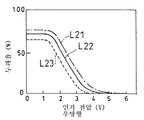
| 시각(θ) | Δn ( 450 ) - Δn ( 650 ) ( ×10-3) | |||||
| 4.5 | 7.0 | 9.0 | 12.0 | 20.0 | 25.0 | |
| #100 | #1 | #2 | #3 | #4 | #5 | |
| 50° | × | △ | ○ | ○ | ○ | ○ |
| 60° | × | × | △ | ○ | ○ | ○ |
| 70° | × | × | × | △ | ○ | ○ |
| 시각(θ) | Δn ( 450 ) - Δn ( 650 ) ( × 10-3) | |||||
| 0 | 3.0 | 4.5 | 5.5 | 7.0 | 9.0 | |
| #21 | #22 | #23 | #24 | #25 | #200 | |
| 50° | ○ | ○ | ○ | ○ | △ | × |
| 60° | ○ | ○ | ○ | △ | × | × |
| 70° | ○ | ○ | ○ | × | × | × |
Claims (28)
- 액정 표시 장치에 있어서,대향하는 표면에 투명 전극층 및 배향막이 각각 형성된 한쌍의 투광성 기판과, 상기 투광성 기판들의 사이에 끼워져 있고 광의 파장에 대한 굴절률 이방성의 변화가 시각(viewing angle)에 의존한 액정 화면의 착색이 발생하지 않는 범위로 설정되어 있는 액정 재료로 이루어진 액정층을 갖는 액정 표시 소자,상기 액정 표시 소자의 양측에 배치되는 한쌍의 편광자, 및상기 액정 표시 소자와 적어도 한쪽의 상기 편광자와의 사이에 적어도 한장 개재된 위상차판을 구비하되,상기 위상차판에서 3개의 주굴절률 na, nb, nc가 na<nb<nc의 관계를 가지며, 상기 주굴절률 nb가 상기 위상차판 표면의 법선에 대해 경사져 있는 액정 표시 장치.
- 제1항에 있어서, 상기 액정 재료의 파장 550nm의 광에 대한 굴절률 이방성 Δn(550)이 0.060보다는 크고 0.120보다는 작은 범위로 설정되어 있는 것을 특징으로 하는 액정 표시 장치.
- 제2항에 있어서, 상기 굴절률 이방성 Δn(550)이 0.065 이상 0.115 이하의 범위로 설정되어 있는 것을 특징으로 하는 액정 표시 장치.
- 제3항에 있어서, 상기 굴절률 이방성 Δn(550)이 0.070 이상 0.095 이하의 범위로 설정되어 있는 것을 특징으로 하는 액정 표시 장치.
- 제1항에 있어서, 모든 위상차판에서 상기 주굴절률 nb의 경사각이 15°와 75°의 사이로 설정되어 있는 것을 특징으로 하는 액정 표시 장치.
- 제1항에 있어서, 상기 액정 재료의 파장 450nm의 광에 대한 굴절률 이방성 Δn(450)과 파장 650nm의 광에 대한 굴절률 이방성 Δn(650)과의 차 Δn(450) - Δn(650)이 0.0070 이상 0.0250 이하의 범위로 설정되어 있는 것을 특징으로 하는 액정 표시 장치.
- 제6항에 있어서, 상기 차 Δn(450) - Δn(650)이 0.0200 이상 0.0250 이하의 범위로 설정되어 있는 것을 특징으로 하는 액정 표시 장치.
- 제6항에 있어서, 모든 위상차판에서 상기 주굴절률 nb의 경사각이 15°와 75°의 사이로 설정되어 있는 것을 특징으로 하는 액정 표시 장치.
- 제6항에 있어서, 상기 액정 재료의 파장 550nm의 광에 대한 굴절률 이방성 Δn(550)이 0.060보다는 크고 0.120보다는 작은 범위로 설정되어 있는 것을 특징으로 하는 액정 표시 장치.
- 제9항에 있어서, 상기 굴절률 이방성 Δn(550)이 0.065 이상 0.115 이하의 범위로 설정되어 있는 것을 특징으로 하는 액정 표시 장치.
- 제10항에 있어서, 상기 굴절률 이방성 Δn(550)이 0.070 이상 0.095 이하의 범위로 설정되어 있는 것을 특징으로 하는 액정 표시 장치.
- 제9항에 있어서, 모든 위상차판에서 상기 주굴절률 nb의 경사각이 15°와 75°의 사이로 설정되어 있는 것을 특징으로 하는 액정 표시 장치.
- 제12항에 있어서, 상기 위상차판은,투명한 유기 고분자로 이루어진 지지체, 및경사 배향되고 가교됨으로써 상기 지지체상에 형성되어 있는 액정 폴리머의 층을 구비하는 것을 특징으로 하는 액정 표시 장치.
- 제12항에 있어서, 상기 위상차판은,투명한 유기 고분자로 이루어진 지지체, 및하이브리드 배향되고 가교됨으로써 상기 지지체상에 형성되어 있는 액정 폴리머의 층을 구비하는 것을 특징으로 하는 액정 표시 장치.
- 액정 표시 장치에 있어서,대향하는 표면에 투명 전극층 및 배향막이 각각 형성된 한쌍의 투광성 기판과, 상기 투광성 기판들의 사이에 끼워져 있고 광의 파장에 대한 굴절률 이방성의 변화가 시각에 의존한 액정 화면의 착색이 발생하지 않는 범위로 설정되어 있는 액정 재료로 이루어진 액정층을 갖는 액정 표시 소자,상기 액정 표시 소자의 양측에 배치되는 한쌍의 편광자, 및상기 액정 표시 소자와 상기 편광자와의 사이에 적어도 한장 개재된 위상차판을 구비하되,상기 위상차판에서 3개의 주굴절률 na, nb, nc가 na= nc> nb의 관계를 가지며, 상기 주굴절률 na및 nc는 상기 위상차판 표면과 평행하고, 상기 주굴절률 nb는 표면의 법선 방향에 평행한 것을 특징으로 하는 액정 표시 장치.
- 제15항에 있어서, 모든 위상차판에서, 상기 주굴절률 na와 상기 주굴절률 nb의 차와 상기 위상차판의 두께 d와의 곱 (na- nb)×d가 80nm와 250nm 사이로 설정되어 있는 것을 특징으로 하는 액정 표시 장치.
- 제15항에 있어서, 상기 액정층에서의 액정 재료의 파장 550nm의 광에 대한 굴절률 이방성 Δn(550)이 0.060보다는 크고 0.120보다는 작은 범위로 설정되어 있는 것을 특징으로 하는 액정 표시 장치.
- 제17항에 있어서, 상기 굴절률 이방성 Δn(550)이 0.065 이상 0.115 이하의 범위로 설정되어 있는 것을 특징으로 하는 액정 표시 장치.
- 제18항에 있어서, 상기 굴절률 이방성 Δn(550)이 0.070 이상 0.095 이하의 범위로 설정되어 있는 것을 특징으로 하는 액정 표시 장치.
- 제17항에 있어서, 모든 위상차판에서, 상기 주굴절률 na와 상기 주굴절률 nb의 차와 상기 위상차판의 두께 d와의 곱 (na- nb)×d가 80nm와 250nm 사이로 설정되어 있는 것을 특징으로 하는 액정 표시 장치.
- 제15항에 있어서, 상기 액정 재료의 파장 450nm의 광에 대한 굴절률 이방성 Δn(450)과 파장 650nm의 광에 대한 굴절률 이방성 Δn(650)과의 차 Δn(450) - Δn(650)이 0 이상 0.0090 미만의 범위로 설정되어 있는 것을 특징으로 하는 액정 표시 장치.
- 제21항에 있어서, 상기 차 Δn(450) - Δn(650)이 0 이상 0.0045 이하의 범위로 설정되어 있는 것을 특징으로 하는 액정 표시 장치.
- 제21항에 있어서, 모든 위상차판에서, 상기 주굴절률 na와 상기 주굴절률 nb의 차와 상기 위상차판의 두께 d와의 곱 (na- nb)×d가 80nm와 250nm 사이로 설정되어 있는 것을 특징으로 하는 액정 표시 장치.
- 제21항에 있어서, 상기 액정층에서의 액정 재료의 파장 550nm의 광에 대한 굴절률 이방성 Δn(550)이 0.060보다는 크고 0.120보다는 작은 범위로 설정되어 있는 것을 특징으로 하는 액정 표시 장치.
- 제24항에 있어서, 상기 굴절률 이방성 Δn(550)이 0.065 이상 0.115 이하의 범위로 설정되어 있는 것을 특징으로 하는 액정 표시 장치.
- 제25항에 있어서, 상기 굴절률 이방성 Δn(550)이 0.070 이상 0.095 이하의 범위로 설정되어 있는 것을 특징으로 하는 액정 표시 장치.
- 제24항에 있어서, 모든 위상차판에서, 상기 주굴절률 na와 상기 주굴절률 nb의 차와 상기 위상차판의 두께 d와의 곱 (na- nb)×d가 80nm와 250nm 사이로 설정되어 있는 것을 특징으로 하는 액정 표시 장치.
- 제27항에 있어서, 상기 위상차판은,투명한 유기 고분자로 이루어진 지지체, 및수평 배향되고 가교됨으로써 상기 지지체상에 형성되어 있는 디스코틱 액정층(discotic liquid crystal layer)을 구비하는 것을 특징으로 하는 액정 표시 장치.
Applications Claiming Priority (4)
| Application Number | Priority Date | Filing Date | Title |
|---|---|---|---|
| JP96-346046 | 1996-12-25 | ||
| JP34603596A JP3452743B2 (ja) | 1996-12-25 | 1996-12-25 | 液晶表示装置 |
| JP34604696A JP3452744B2 (ja) | 1996-12-25 | 1996-12-25 | 液晶表示装置 |
| JP96-346035 | 1996-12-25 |
Publications (2)
| Publication Number | Publication Date |
|---|---|
| KR19980064518A KR19980064518A (ko) | 1998-10-07 |
| KR100290267B1 true KR100290267B1 (ko) | 2001-05-15 |
Family
ID=27806846
Family Applications (1)
| Application Number | Title | Priority Date | Filing Date |
|---|---|---|---|
| KR1019970072507A Expired - Fee Related KR100290267B1 (ko) | 1996-12-25 | 1997-12-23 | 액정표시장치 |
Country Status (3)
| Country | Link |
|---|---|
| US (2) | US6839110B1 (ko) |
| KR (1) | KR100290267B1 (ko) |
| TW (1) | TW515925B (ko) |
Families Citing this family (5)
| Publication number | Priority date | Publication date | Assignee | Title |
|---|---|---|---|---|
| JP4032568B2 (ja) * | 1999-06-30 | 2008-01-16 | カシオ計算機株式会社 | 液晶表示装置 |
| US20040219305A1 (en) * | 2003-02-13 | 2004-11-04 | Fuji Photo Film Co., Ltd. | Retardation film and elliptically polarizing film |
| JP2005107501A (ja) * | 2003-09-09 | 2005-04-21 | Toshiba Matsushita Display Technology Co Ltd | 液晶表示装置 |
| CN102707491A (zh) * | 2011-11-30 | 2012-10-03 | 京东方科技集团股份有限公司 | 液晶显示器和其视角补偿方法 |
| KR102245610B1 (ko) * | 2015-01-09 | 2021-04-28 | 삼성디스플레이 주식회사 | 액정 표시 장치 |
Citations (2)
| Publication number | Priority date | Publication date | Assignee | Title |
|---|---|---|---|---|
| JPS55600A (en) * | 1978-06-08 | 1980-01-05 | American Liquid Xtal Chem | Liquid crystal optical shutter |
| JPH0675116A (ja) * | 1992-06-26 | 1994-03-18 | Sharp Corp | 位相差板および液晶表示装置 |
Family Cites Families (22)
| Publication number | Priority date | Publication date | Assignee | Title |
|---|---|---|---|---|
| JPS5697318A (en) | 1980-01-07 | 1981-08-06 | Hitachi Ltd | Liquid-crystal display element |
| WO1990011546A1 (en) | 1989-03-28 | 1990-10-04 | Asahi Glass Company Ltd. | Liquid crystal display device |
| US5184236A (en) * | 1990-08-10 | 1993-02-02 | Casio Computer Co., Ltd. | Twisted nematic liquid crystal display device with retardation plates having phase axis direction within 15° of alignment direction |
| DE69209448T2 (de) * | 1991-06-17 | 1996-08-01 | Fujimori Kogyo Co | Phasendifferenz-film, phasendifferenz-platte, und flüssigkristallanzeige, die diese enthält |
| JP3218635B2 (ja) | 1991-08-30 | 2001-10-15 | 大日本インキ化学工業株式会社 | 液晶組成物の調製方法 |
| JP3185313B2 (ja) | 1992-02-07 | 2001-07-09 | セイコーエプソン株式会社 | 液晶表示素子 |
| JP3049623B2 (ja) | 1992-05-12 | 2000-06-05 | 富士通株式会社 | 液晶表示装置 |
| FR2693020B1 (fr) * | 1992-06-26 | 1999-01-22 | Thomson Consumer Electronics | Dispositif d'affichage a cristal liquide nematique en helice. |
| JPH06167706A (ja) | 1992-09-30 | 1994-06-14 | Casio Comput Co Ltd | 液晶表示装置 |
| JP2640083B2 (ja) * | 1993-09-22 | 1997-08-13 | 富士写真フイルム株式会社 | 光学補償シート及びそれを用いた液晶表示装置 |
| DE69421407T2 (de) * | 1993-09-29 | 2000-05-04 | Akzo Nobel N.V., Arnheim/Arnhem | Verzögerungsschicht mit einer an die aktive flüssigkristalzelle angepassten dispersion |
| JP3325973B2 (ja) * | 1993-10-22 | 2002-09-17 | 富士写真フイルム株式会社 | 光学異方素子およびそれを用いた液晶表示素子 |
| US5657140A (en) * | 1993-12-15 | 1997-08-12 | Ois Optical Imaging Systems, Inc. | Normally white twisted nematic LCD with positive and negative retarders |
| KR100267894B1 (ko) * | 1994-05-31 | 2000-10-16 | 무네유키 가코우 | 광학 보상 시이트 및 액정 디스플레이 |
| JPH08101381A (ja) | 1994-09-30 | 1996-04-16 | Fuji Photo Film Co Ltd | 液晶表示素子 |
| JPH08152514A (ja) | 1994-11-28 | 1996-06-11 | Fuji Photo Film Co Ltd | 光学補償シート及びそれを用いた液晶表示素子 |
| US5638200A (en) * | 1995-02-03 | 1997-06-10 | Ois Optical Imaging Systems, Inc. | Liquid crystal display with tilted retardation film |
| JPH09101515A (ja) * | 1995-10-06 | 1997-04-15 | Sharp Corp | 液晶表示装置 |
| KR100405893B1 (ko) * | 1995-10-23 | 2004-10-06 | 가부시끼가이샤 히다치 세이사꾸쇼 | 액정표시장치 |
| DE69627556T2 (de) * | 1995-11-17 | 2004-01-29 | Fuji Photo Film Co Ltd | Flüssigkristallanzeige vom hybriden Ausrichtungstyp |
| JPH10123503A (ja) * | 1996-10-17 | 1998-05-15 | Sharp Corp | 液晶表示装置 |
| US5867239A (en) * | 1997-10-17 | 1999-02-02 | Minnesota Mining And Manufacturing Company | Wide angle optical retarder |
-
1997
- 1997-12-15 TW TW086118905A patent/TW515925B/zh not_active IP Right Cessation
- 1997-12-23 KR KR1019970072507A patent/KR100290267B1/ko not_active Expired - Fee Related
- 1997-12-23 US US08/997,219 patent/US6839110B1/en not_active Expired - Lifetime
-
2004
- 2004-06-16 US US10/870,405 patent/US7088410B2/en not_active Expired - Fee Related
Patent Citations (2)
| Publication number | Priority date | Publication date | Assignee | Title |
|---|---|---|---|---|
| JPS55600A (en) * | 1978-06-08 | 1980-01-05 | American Liquid Xtal Chem | Liquid crystal optical shutter |
| JPH0675116A (ja) * | 1992-06-26 | 1994-03-18 | Sharp Corp | 位相差板および液晶表示装置 |
Also Published As
| Publication number | Publication date |
|---|---|
| KR19980064518A (ko) | 1998-10-07 |
| US6839110B1 (en) | 2005-01-04 |
| US7088410B2 (en) | 2006-08-08 |
| US20040233364A1 (en) | 2004-11-25 |
| TW515925B (en) | 2003-01-01 |
Similar Documents
| Publication | Publication Date | Title |
|---|---|---|
| KR100327518B1 (ko) | 액정표시장치 | |
| KR100306177B1 (ko) | 액정표시장치 | |
| KR100277144B1 (ko) | 액정 표시 장치 | |
| KR100269678B1 (ko) | 액정 표시 장치 | |
| KR100290695B1 (ko) | 액정표시장치 | |
| KR100304226B1 (ko) | 액정표시장치 | |
| KR100290267B1 (ko) | 액정표시장치 | |
| JP3599176B2 (ja) | 液晶表示装置 | |
| JP3556653B2 (ja) | 液晶表示装置の製造方法 | |
| JP3452743B2 (ja) | 液晶表示装置 | |
| JP3773056B2 (ja) | 液晶表示装置 | |
| JP3452744B2 (ja) | 液晶表示装置 | |
| JP3770400B2 (ja) | 液晶表示装置 | |
| JP3555895B2 (ja) | 液晶表示装置の製造方法 | |
| JP3776433B2 (ja) | 液晶表示装置 | |
| JP3776432B2 (ja) | 液晶表示装置 | |
| JP3555894B2 (ja) | 液晶表示装置の製造方法 | |
| JP3770401B2 (ja) | 液晶表示装置 | |
| JP3452478B2 (ja) | 液晶表示装置 | |
| JPH11258591A (ja) | 液晶表示装置 | |
| JP2003202572A (ja) | 液晶表示装置 | |
| JP2003202571A (ja) | 液晶表示装置 |
Legal Events
| Date | Code | Title | Description |
|---|---|---|---|
| A201 | Request for examination | ||
| PA0109 | Patent application |
St.27 status event code: A-0-1-A10-A12-nap-PA0109 |
|
| PA0201 | Request for examination |
St.27 status event code: A-1-2-D10-D11-exm-PA0201 |
|
| R17-X000 | Change to representative recorded |
St.27 status event code: A-3-3-R10-R17-oth-X000 |
|
| PG1501 | Laying open of application |
St.27 status event code: A-1-1-Q10-Q12-nap-PG1501 |
|
| PN2301 | Change of applicant |
St.27 status event code: A-3-3-R10-R13-asn-PN2301 St.27 status event code: A-3-3-R10-R11-asn-PN2301 |
|
| E902 | Notification of reason for refusal | ||
| PE0902 | Notice of grounds for rejection |
St.27 status event code: A-1-2-D10-D21-exm-PE0902 |
|
| P11-X000 | Amendment of application requested |
St.27 status event code: A-2-2-P10-P11-nap-X000 |
|
| P13-X000 | Application amended |
St.27 status event code: A-2-2-P10-P13-nap-X000 |
|
| E701 | Decision to grant or registration of patent right | ||
| PE0701 | Decision of registration |
St.27 status event code: A-1-2-D10-D22-exm-PE0701 |
|
| GRNT | Written decision to grant | ||
| PR0701 | Registration of establishment |
St.27 status event code: A-2-4-F10-F11-exm-PR0701 |
|
| PR1002 | Payment of registration fee |
St.27 status event code: A-2-2-U10-U11-oth-PR1002 Fee payment year number: 1 |
|
| PG1601 | Publication of registration |
St.27 status event code: A-4-4-Q10-Q13-nap-PG1601 |
|
| PR1001 | Payment of annual fee |
St.27 status event code: A-4-4-U10-U11-oth-PR1001 Fee payment year number: 4 |
|
| PR1001 | Payment of annual fee |
St.27 status event code: A-4-4-U10-U11-oth-PR1001 Fee payment year number: 5 |
|
| PN2301 | Change of applicant |
St.27 status event code: A-5-5-R10-R13-asn-PN2301 St.27 status event code: A-5-5-R10-R11-asn-PN2301 |
|
| PR1001 | Payment of annual fee |
St.27 status event code: A-4-4-U10-U11-oth-PR1001 Fee payment year number: 6 |
|
| PR1001 | Payment of annual fee |
St.27 status event code: A-4-4-U10-U11-oth-PR1001 Fee payment year number: 7 |
|
| R17-X000 | Change to representative recorded |
St.27 status event code: A-5-5-R10-R17-oth-X000 |
|
| PR1001 | Payment of annual fee |
St.27 status event code: A-4-4-U10-U11-oth-PR1001 Fee payment year number: 8 |
|
| PR1001 | Payment of annual fee |
St.27 status event code: A-4-4-U10-U11-oth-PR1001 Fee payment year number: 9 |
|
| PR1001 | Payment of annual fee |
St.27 status event code: A-4-4-U10-U11-oth-PR1001 Fee payment year number: 10 |
|
| PR1001 | Payment of annual fee |
St.27 status event code: A-4-4-U10-U11-oth-PR1001 Fee payment year number: 11 |
|
| FPAY | Annual fee payment |
Payment date: 20120130 Year of fee payment: 12 |
|
| PR1001 | Payment of annual fee |
St.27 status event code: A-4-4-U10-U11-oth-PR1001 Fee payment year number: 12 |
|
| FPAY | Annual fee payment |
Payment date: 20130201 Year of fee payment: 13 |
|
| PR1001 | Payment of annual fee |
St.27 status event code: A-4-4-U10-U11-oth-PR1001 Fee payment year number: 13 |
|
| LAPS | Lapse due to unpaid annual fee | ||
| PC1903 | Unpaid annual fee |
St.27 status event code: A-4-4-U10-U13-oth-PC1903 Not in force date: 20140301 Payment event data comment text: Termination Category : DEFAULT_OF_REGISTRATION_FEE |
|
| PC1903 | Unpaid annual fee |
St.27 status event code: N-4-6-H10-H13-oth-PC1903 Ip right cessation event data comment text: Termination Category : DEFAULT_OF_REGISTRATION_FEE Not in force date: 20140301 |
|
| R18-X000 | Changes to party contact information recorded |
St.27 status event code: A-5-5-R10-R18-oth-X000 |
|
| P22-X000 | Classification modified |
St.27 status event code: A-4-4-P10-P22-nap-X000 |