KR100235590B1 - 박막트랜지스터 액정표시장치의 구동방법 - Google Patents
박막트랜지스터 액정표시장치의 구동방법 Download PDFInfo
- Publication number
- KR100235590B1 KR100235590B1 KR1019970000294A KR19970000294A KR100235590B1 KR 100235590 B1 KR100235590 B1 KR 100235590B1 KR 1019970000294 A KR1019970000294 A KR 1019970000294A KR 19970000294 A KR19970000294 A KR 19970000294A KR 100235590 B1 KR100235590 B1 KR 100235590B1
- Authority
- KR
- South Korea
- Prior art keywords
- drain
- source
- gate
- terminal
- contact
- Prior art date
- Legal status (The legal status is an assumption and is not a legal conclusion. Google has not performed a legal analysis and makes no representation as to the accuracy of the status listed.)
- Expired - Lifetime
Links
Images


Classifications
-
- G—PHYSICS
- G11—INFORMATION STORAGE
- G11C—STATIC STORES
- G11C19/00—Digital stores in which the information is moved stepwise, e.g. shift registers
- G11C19/18—Digital stores in which the information is moved stepwise, e.g. shift registers using capacitors as main elements of the stages
- G11C19/182—Digital stores in which the information is moved stepwise, e.g. shift registers using capacitors as main elements of the stages in combination with semiconductor elements, e.g. bipolar transistors, diodes
- G11C19/184—Digital stores in which the information is moved stepwise, e.g. shift registers using capacitors as main elements of the stages in combination with semiconductor elements, e.g. bipolar transistors, diodes with field-effect transistors, e.g. MOS-FET
-
- G—PHYSICS
- G09—EDUCATION; CRYPTOGRAPHY; DISPLAY; ADVERTISING; SEALS
- G09G—ARRANGEMENTS OR CIRCUITS FOR CONTROL OF INDICATING DEVICES USING STATIC MEANS TO PRESENT VARIABLE INFORMATION
- G09G3/00—Control arrangements or circuits, of interest only in connection with visual indicators other than cathode-ray tubes
- G09G3/20—Control arrangements or circuits, of interest only in connection with visual indicators other than cathode-ray tubes for presentation of an assembly of a number of characters, e.g. a page, by composing the assembly by combination of individual elements arranged in a matrix no fixed position being assigned to or needed to be assigned to the individual characters or partial characters
- G09G3/34—Control arrangements or circuits, of interest only in connection with visual indicators other than cathode-ray tubes for presentation of an assembly of a number of characters, e.g. a page, by composing the assembly by combination of individual elements arranged in a matrix no fixed position being assigned to or needed to be assigned to the individual characters or partial characters by control of light from an independent source
- G09G3/36—Control arrangements or circuits, of interest only in connection with visual indicators other than cathode-ray tubes for presentation of an assembly of a number of characters, e.g. a page, by composing the assembly by combination of individual elements arranged in a matrix no fixed position being assigned to or needed to be assigned to the individual characters or partial characters by control of light from an independent source using liquid crystals
- G09G3/3611—Control of matrices with row and column drivers
- G09G3/3674—Details of drivers for scan electrodes
- G09G3/3677—Details of drivers for scan electrodes suitable for active matrices only
-
- G—PHYSICS
- G09—EDUCATION; CRYPTOGRAPHY; DISPLAY; ADVERTISING; SEALS
- G09G—ARRANGEMENTS OR CIRCUITS FOR CONTROL OF INDICATING DEVICES USING STATIC MEANS TO PRESENT VARIABLE INFORMATION
- G09G2310/00—Command of the display device
- G09G2310/02—Addressing, scanning or driving the display screen or processing steps related thereto
- G09G2310/0264—Details of driving circuits
- G09G2310/0281—Arrangement of scan or data electrode driver circuits at the periphery of a panel not inherent to a split matrix structure
Landscapes
- Engineering & Computer Science (AREA)
- Microelectronics & Electronic Packaging (AREA)
- Chemical & Material Sciences (AREA)
- Crystallography & Structural Chemistry (AREA)
- Physics & Mathematics (AREA)
- Computer Hardware Design (AREA)
- General Physics & Mathematics (AREA)
- Theoretical Computer Science (AREA)
- Power Engineering (AREA)
- Control Of Indicators Other Than Cathode Ray Tubes (AREA)
- Shift Register Type Memory (AREA)
- Liquid Crystal Display Device Control (AREA)
Abstract
Description
Claims (7)
- 기판 위에 복수개의 주사선이 열(列:row)로, 복수개의 신호선이 행(行:column)으로 서로 교차하여 형성되고, 상기 주사선과 상기 신호선 각각의 교차부에 박막트랜지스터와 화소가 설치된 TFT어레이와; 상기 주사선 구동회로가 구비되어있는 액정패널에 있어서; 상기 주사선 구동회로는 소정의 주기로 set신호를 인가받는 단자1 및 reset 신호를 인가받는 단자2와, 상기 단자1과 단자2에 인가되는 신호에 따라 구동신호를 주사선에 인가하는 출력단자와, 쉬프트신호를 인가받는 쉬프트입력단자와, 상기 쉬프트신호를 출력하고, 인접하는 다른 스테이지의 쉬프트입력단자와 연결되는 쉬프트출력단자와, 상기 쉬프트신호를 reset시키는 신호를 인가받는 쉬프트리셋단자로 구성된 것을 특징으로하는 액정패널.
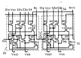
- 1항에 있어서, 상기 구동회로는상기 단자1에 게이트가 연결되고, 상기 쉬프트입력단자에 소스가 연결된 트랜지스터 M1과상기 단자2에 게이트가 연결되고, 상기 M1의 드레인에 소스가 연결되고, 접지전압 Vee에 드레인이 연결된 트랜지스터 M2와상기 단자2에 게이트가 연결되고, 외부전압 Vcc에 소스가 연결된 트랜지스터 M3과상기 단자1에 게이트가 연결되고, 상기 접지전압 Vee에 드레인이 연결된 트랜지스터 M4와상기 M1의 드레인과 상기 M2의 소스 사이의 접점 a에 게이트가 연결되고, 외부전압 Vcc에 소스가 연결된 트랜지스터 M5와상기 M3의 소스와 상기 M4의 드레인 사이의 접점 b에 게이트가 연결되고, 상기 M5의 드레인에 소스가 연결되며, 상기 접지전압 Vee에 드레인이 연결된 트랜지스터 M6과상기 접점 a와 상기 M5의 게이트 사이의 접점 d에 한쪽 전극이 연결되고, 상기 접지전압 Vee에 다른쪽 전극이 연결된 캐패시터 Ch1과상기 접점 b와 상기 M6의 게이트 사이의 접점 e에 한쪽 전극이 연결되고, 상기 접지전압 Vee에 다른쪽 전극이 연결된 캐패시터 Cs1과상기 M5의 드레인과 상기 M6의 소스 사이의 접점 h에 연결된 출력단자로 구성된 출력신호부와;상기 단자1에 게이트가 연결되고, 상기 쉬프트입력단자에 소스가 연결된 트랜지스터 M7과상기 쉬프트리셋단자에 게이트가 연결되고, 상기 M7의 드레인에 소스가 연결되며, 상기 접지전압 Vee에 드레인이 연결된 트랜지스터 M8과상기 쉬프트리셋단자에 게이트가 연결되고, 상기 외부전압 Vcc에 소스가 연결된 트랜지스터 M9와상기 단자1에 게이트가 연결되고, 상기 M9의 드레인에 소스가 연결되며, 상기 접지전압 Vee에 드레인이 연결된 트랜지스터 M10과상기 M7의 드레인과 상기 M8의 소스 사이의 접점 c에 게이트가 연결되고, 상기 외부전압 Vcc에 소스가 연결된 트랜지스터 M11과상기 M9의 소스와 상기 M10의 드레인 사이의 접점 d에 게이트가 연결되고, 상기 M11의 드레인에 소스가 연결되며, 상기 접지전압 Vee에 드레인이 연결된 트랜지스터 M12와상기 접점 c와 상기 M11의 게이트 사이의 접점 f에 한쪽 전극이 연결되고, 상기 접지전압 Vee에 다른쪽 전극이 연결된 캐패시터 Ch2와상기 접점 d와 상기 M12의 게이트 사이의 접점 g에 한쪽 전극이 연결되고, 상기 접지전압 Vee에 다른쪽 전극이 연결된 캐패시터 Cs2와상기 M11의 드레인과 상기 M12의 소스 사이의 접점 i에 연결된 쉬프트출력단자로 구성된 쉬프트출력부를 포함하는 구조로 된 주사선선택구동회로인 것을 특징으로 하는 액정패널.
- 1항에 있어서, 상기 구동회로는상기 단자1에 게이트가 연결되고, 상기 쉬프트입력단자에 소스가 연결된 트랜지스터 M1과상기 단자2에 게이트가 연결되고, 상기 M1의 드레인에 소스가 연결되고, 접지전압 Vee에 드레인이 연결된 트랜지스터 M2와상기 단자2에 게이트가 연결되고, 외부전압 Vcc에 소스가 연결된 트랜지스터 M3과상기 단자1에 게이트가 연결되고, 상기 접지전압 Vee에 드레인이 연결된 트랜지스터 M4와상기 M1의 드레인과 상기 M2의 소스 사이의 접점 a에 게이트가 연결되고, 외부전압 Vcc에 소스가 연결된 트랜지스터 M5와상기 M3의 소스와 상기 M4의 드레인 사이의 접점 b에 게이트가 연결되고, 상기 M5의 드레인에 소스가 연결되며, 상기 접지전압 Vee에 드레인이 연결된 트랜지스터 M6과상기 접점 a와 상기 M5의 게이트 사이의 접점 d에 한쪽 전극이 연결되고, 상기 접지전압 Vee에 다른쪽 전극이 연결된 캐패시터 Ch1과상기 접점 b와 상기 M6의 게이트 사이의 접점 e에 한쪽 전극이 연결되고, 상기 접지전압 Vee에 다른쪽 전극이 연결된 캐패시터 Cs1과상기 M5의 드레인과 상기 M6의 소스 사이의 접점 h에 연결된 출력단자로 구성된 출력신호부와;상기 단자1에 게이트가 연결되고, 상기 쉬프트입력단자에 소스가 연결된 트랜지스터 M7과상기 쉬프트리셋단자에 게이트가 연결되고, 상기 M7의 드레인에 소스가 연결되며, 상기 접지전압 Vee에 드레인이 연결된 트랜지스터 M8과상기 쉬프트리셋단자에 게이트가 연결되고, 상기 외부전압 Vcc에 소스가 연결된 트랜지스터 M9와상기 단자1에 게이트가 연결되고, 상기 M9의 드레인에 소스가 연결되며, 상기 접지전압 Vee에 드레인이 연결된 트랜지스터 M10과상기 M7의 드레인과 상기 M8의 소스 사이의 접점 c에 게이트가 연결되고, 상기 외부전압 Vcc에 소스가 연결된 트랜지스터 M11과상기 M9의 소스와 상기 M10의 드레인 사이의 접점 d에 게이트가 연결되고, 상기 M11의 드레인에 소스가 연결되며, 상기 접지전압 Vee에 드레인이 연결된 트랜지스터 M12와상기 접점 c와 상기 M11의 게이트 사이의 접점 f에 한쪽 전극이 연결되고, 상기 접지전압 Vee에 다른쪽 전극이 연결된 캐패시터 Ch2와상기 접점 d와 상기 M12의 게이트 사이의 접점 g에 한쪽 전극이 연결되고, 상기 접지전압 Vee에 다른쪽 전극이 연결된 캐패시터 Cs2와상기 M11의 드레인과 상기 M12의 소스 사이의 접점 i에 연결된 쉬프트출력단자로 구성된 쉬프트출력부를 포함하는 구조로 된 주사선선택구동회로인 것을 특징으로 하는 액정패널.
- 복수개의 주사선이 열(列:row)로, 복수개의 신호선이 행(行:column)으로 서로 교차하여 형성되고,상기 주사선과 상기 신호선 각각의 교차부에 박막트랜지스터 및 화소가 설치되고,상기 주사선 각각의 양끝단에 연결된 스위칭수단1 및 스위칭수단2와,상기 스위칭수단1 및 스위칭수단2 각각에 주사선선택구동회로가 하나 이상 연결되어 형성되고, 상기 스위칭수단1 및 스위칭수단2를 도통시키는 신호가 입력되는 스위칭단자와, 상기 주사선에 연결된 드레인과, 상기 주사선선택구동회로의 출력단자에 연결된 소스와, 상기 스위칭단자에 연결된 게이트로 구성된 박막트랜지스터가 상기 주사선의 개수와 동일하게 형성되어 이루어지는 것을 특징으로하는 액정패널.
- 제1항에 있어서, 상기 쉬프트신호를 reset시키는 신호를 인가받는 쉬프트리셋단자로 구성된 구동회로가 상기 구동신호를 상기 주사선에 인가하는 동작을 스위칭하는 수단을 포함하여 하나의 스테이지로 구성되고, 그 구동회로는 하나 이상 병렬로 연결되어 이루어지는 것을 특징으로하는 액정패널.
- 5항에 있어서, 상기 구동회로는단자1에 게이트가 연결되고, 상기 쉬프트입력단자에 소스가 연결된 트랜지스터 M1과,단자2에 게이트가 연결되고, 상기 M1의 드레인에 소스가 연결되고, 접지전압 Vee에 드레인이 연결된 트랜지스터 M2와,상기 단자2에 게이트가 연결되고, 외부전압 Vcc에 소스가 연결된 트랜지스터 M3과상기 단자1에 게이트가 연결되고, 상기 접지전압 Vee에 드레인이 연결된 트랜지스터 M4와,상기 M1의 드레인과 상기 M2의 소스 사이의 접점 a에 게이트가 연결되고, 외부전압 Vcc에 소스가 연결된 트랜지스터 M5와,상기 M3의 소스와 상기 M4의 드레인 사이의 접점 b에 게이트가 연결되고, 상기 M5의 드레인에 소스가 연결되며, 상기 접지전압 Vee에 드레인이 연결된 트랜지스터 M6과,상기 접점 a와 상기 M5의 게이트 사이의 접점 d에 한쪽 전극이 연결되고, 상기 접지전압 Vee에 다른쪽 전극이 연결된 캐패시터 Ch1과,상기 접점 b와 상기 M6의 게이트 사이의 접점 e에 한쪽 전극이 연결되고, 상기 접지전압 Vee에 다른쪽 전극이 연결된 캐패시터 Cs1과,상기 M5의 드레인과 상기 M6의 소스 사이의 접점 h에 연결된 출력단자로 구성된 출력신호부와;상기 단자1에 게이트가 연결되고, 상기 쉬프트입력단자에 소스가 연결된 트랜지스터 M7과,상기 쉬프트리셋단자에 게이트가 연결되고, 상기 M7의 드레인에 소스가 연결되며, 상기 접지전압 Vee에 드레인이 연결된 트랜지스터 M8과,상기 쉬프트리셋단자에 게이트가 연결되고, 상기 외부전압 Vcc에 소스가 연결된 트랜지스터 M9와,상기 단자1에 게이트가 연결되고, 상기 M9의 드레인에 소스가 연결되며, 상기 접지전압 Vee에 드레인이 연결된 트랜지스터 M10과,상기 M7의 드레인과 상기 M8의 소스 사이의 접점 c에 게이트가 연결되고, 상기 외부전압 Vcc에 소스가 연결된 트랜지스터 M11과,상기 M9의 소스와 상기 M10의 드레인 사이의 접점 d에 게이트가 연결되고, 상기 M11의 드레인에 소스가 연결되며, 상기 접지전압 Vee에 드레인이 연결된 트랜지스터 M12와,상기 접점 c와 상기 M11의 게이트 사이의 접점 f에 한쪽 전극이 연결되고, 상기 접지전압 Vee에 다른쪽 전극이 연결된 캐패시터 Ch2와,상기 접점 d와 상기 M12의 게이트 사이의 접점 g에 한쪽 전극이 연결되고, 상기 접지전압 Vee에 다른쪽 전극이 연결된 캐패시터 Cs2와,상기 M11의 드레인과 상기 M12의 소스 사이의 접점 i에 연결된 쉬프트출력단자로 구성된 쉬프트출력부를 포함하는 구조로 이루어진 것을 특징으로하는 액정패널.
- 7항에 있어서, 상기 구동회로는단자1에 게이트가 연결되고, 상기 쉬프트입력단자에 소스가 연결된 트랜지스터 M1과,단자2에 게이트가 연결되고, 상기 M1의 드레인에 소스가 연결되고, 접지전압 Vee에 드레인이 연결된 트랜지스터 M2와,상기 단자2에 게이트가 연결되고, 외부전압 Vcc에 소스가 연결된 트랜지스터 M3과상기 단자1에 게이트가 연결되고, 상기 접지전압 Vee에 드레인이 연결된 트랜지스터 M4와,상기 M1의 드레인과 상기 M2의 소스 사이의 접점 a에 게이트가 연결되고, 외부전압 Vcc에 소스가 연결된 트랜지스터 M5와,상기 M3의 소스와 상기 M4의 드레인 사이의 접점 b에 게이트가 연결되고, 상기 M5의 드레인에 소스가 연결되며, 상기 접지전압 Vee에 드레인이 연결된 트랜지스터 M6과,상기 접점 a와 상기 M5의 게이트 사이의 접점 d에 한쪽 전극이 연결되고, 상기 접지전압 Vee에 다른쪽 전극이 연결된 캐패시터 Ch1과,상기 접점 b와 상기 M6의 게이트 사이의 접점 e에 한쪽 전극이 연결되고, 상기 접지전압 Vee에 다른쪽 전극이 연결된 캐패시터 Cs1과,상기 M5의 드레인과 상기 M6의 소스 사이의 접점 h에 연결된 출력단자로 구성된 출력신호부와;상기 단자1에 게이트가 연결되고, 상기 쉬프트입력단자에 소스가 연결된 트랜지스터 M7과,상기 쉬프트리셋단자에 게이트가 연결되고, 상기 M7의 드레인에 소스가 연결되며, 상기 접지전압 Vee에 드레인이 연결된 트랜지스터 M8과,상기 쉬프트리셋단자에 게이트가 연결되고, 상기 외부전압 Vcc에 소스가 연결된 트랜지스터 M9와,상기 단자1에 게이트가 연결되고, 상기 M9의 드레인에 소스가 연결되며, 상기 접지전압 Vee에 드레인이 연결된 트랜지스터 M10과,상기 M7의 드레인과 상기 M8의 소스 사이의 접점 c에 게이트가 연결되고, 상기 외부전압 Vcc에 소스가 연결된 트랜지스터 M11과,상기 M9의 소스와 상기 M10의 드레인 사이의 접점 d에 게이트가 연결되고, 상기 M11의 드레인에 소스가 연결되며, 상기 접지전압 Vee에 드레인이 연결된 트랜지스터 M12와,상기 접점 c와 상기 M11의 게이트 사이의 접점 f에 한쪽 전극이 연결되고, 상기 접지전압 Vee에 다른쪽 전극이 연결된 캐패시터 Ch2와,상기 접점 d와 상기 M12의 게이트 사이의 접점 g에 한쪽 전극이 연결되고, 상기 접지전압 Vee에 다른쪽 전극이 연결된 캐패시터 Cs2와,상기 M11의 드레인과 상기 M12의 소스 사이의 접점 i에 연결된 쉬프트출력단자로 구성된 쉬프트출력부를 포함하는 구조로 이루어진 것을 특징으로하는 액정패널.
Priority Applications (2)
| Application Number | Priority Date | Filing Date | Title |
|---|---|---|---|
| KR1019970000294A KR100235590B1 (ko) | 1997-01-08 | 1997-01-08 | 박막트랜지스터 액정표시장치의 구동방법 |
| US08/997,303 US6091393A (en) | 1997-01-08 | 1997-12-23 | Scan driver IC for a liquid crystal display |
Applications Claiming Priority (1)
| Application Number | Priority Date | Filing Date | Title |
|---|---|---|---|
| KR1019970000294A KR100235590B1 (ko) | 1997-01-08 | 1997-01-08 | 박막트랜지스터 액정표시장치의 구동방법 |
Publications (2)
| Publication Number | Publication Date |
|---|---|
| KR19980065363A KR19980065363A (ko) | 1998-10-15 |
| KR100235590B1 true KR100235590B1 (ko) | 1999-12-15 |
Family
ID=19494282
Family Applications (1)
| Application Number | Title | Priority Date | Filing Date |
|---|---|---|---|
| KR1019970000294A Expired - Lifetime KR100235590B1 (ko) | 1997-01-08 | 1997-01-08 | 박막트랜지스터 액정표시장치의 구동방법 |
Country Status (2)
| Country | Link |
|---|---|
| US (1) | US6091393A (ko) |
| KR (1) | KR100235590B1 (ko) |
Families Citing this family (26)
| Publication number | Priority date | Publication date | Assignee | Title |
|---|---|---|---|---|
| JP3680601B2 (ja) * | 1998-05-14 | 2005-08-10 | カシオ計算機株式会社 | シフトレジスタ、表示装置、撮像素子駆動装置及び撮像装置 |
| US6476785B1 (en) * | 1999-11-08 | 2002-11-05 | Atmel Corporation | Drive circuit for liquid crystal display cell |
| JP3301422B2 (ja) * | 1999-11-08 | 2002-07-15 | 日本電気株式会社 | ディスプレイの駆動方法及びその回路 |
| JP4785271B2 (ja) * | 2001-04-27 | 2011-10-05 | 株式会社半導体エネルギー研究所 | 液晶表示装置、電子機器 |
| JP4439761B2 (ja) * | 2001-05-11 | 2010-03-24 | 株式会社半導体エネルギー研究所 | 液晶表示装置、電子機器 |
| TW582005B (en) | 2001-05-29 | 2004-04-01 | Semiconductor Energy Lab | Pulse output circuit, shift register, and display device |
| SG119161A1 (en) * | 2001-07-16 | 2006-02-28 | Semiconductor Energy Lab | Light emitting device |
| US6788108B2 (en) | 2001-07-30 | 2004-09-07 | Semiconductor Energy Laboratory Co., Ltd. | Semiconductor device |
| JP4789369B2 (ja) * | 2001-08-08 | 2011-10-12 | 株式会社半導体エネルギー研究所 | 表示装置及び電子機器 |
| US7218349B2 (en) * | 2001-08-09 | 2007-05-15 | Semiconductor Energy Laboratory Co., Ltd. | Semiconductor device |
| JP3917845B2 (ja) * | 2001-11-16 | 2007-05-23 | シャープ株式会社 | 液晶表示装置 |
| JP4397555B2 (ja) * | 2001-11-30 | 2010-01-13 | 株式会社半導体エネルギー研究所 | 半導体装置、電子機器 |
| JP4016184B2 (ja) * | 2002-05-31 | 2007-12-05 | ソニー株式会社 | データ処理回路、表示装置および携帯端末 |
| JP4339103B2 (ja) | 2002-12-25 | 2009-10-07 | 株式会社半導体エネルギー研究所 | 半導体装置及び表示装置 |
| KR100705628B1 (ko) * | 2003-12-30 | 2007-04-11 | 비오이 하이디스 테크놀로지 주식회사 | 액정표시장치의 구동회로 |
| KR101039983B1 (ko) * | 2005-03-31 | 2011-06-09 | 엘지디스플레이 주식회사 | 게이트 드라이버 및 이를 구비한 표시장치 |
| TWI291153B (en) * | 2005-09-26 | 2007-12-11 | Au Optronics Corp | Display panels, driving method thereof and electronic devices using the same |
| KR101212139B1 (ko) * | 2005-09-30 | 2012-12-14 | 엘지디스플레이 주식회사 | 발광표시장치 |
| US9153341B2 (en) | 2005-10-18 | 2015-10-06 | Semiconductor Energy Laboratory Co., Ltd. | Shift register, semiconductor device, display device, and electronic device |
| JP5116277B2 (ja) | 2006-09-29 | 2013-01-09 | 株式会社半導体エネルギー研究所 | 半導体装置、表示装置、液晶表示装置、表示モジュール及び電子機器 |
| TWI374418B (en) * | 2007-05-15 | 2012-10-11 | Novatek Microelectronics Corp | Method and apparatus to generate control signals for display-panel driver |
| JP4582216B2 (ja) * | 2008-07-12 | 2010-11-17 | ソニー株式会社 | 半導体デバイス、表示パネル及び電子機器 |
| EP2234100B1 (en) | 2009-03-26 | 2016-11-02 | Semiconductor Energy Laboratory Co., Ltd. | Liquid crystal display device |
| KR20130003252A (ko) * | 2011-06-30 | 2013-01-09 | 삼성디스플레이 주식회사 | 스테이지 회로 및 이를 이용한 주사 구동부 |
| KR101878374B1 (ko) * | 2012-04-26 | 2018-07-16 | 삼성디스플레이 주식회사 | 주사 구동 장치 및 그 구동 방법 |
| JP7554673B2 (ja) | 2018-12-20 | 2024-09-20 | 株式会社半導体エネルギー研究所 | 半導体装置 |
Family Cites Families (8)
| Publication number | Priority date | Publication date | Assignee | Title |
|---|---|---|---|---|
| WO1992015931A2 (fr) * | 1991-02-28 | 1992-09-17 | Thomson-Lcd | Registres a decalage redondants pour dispositifs de balayage |
| EP0909975B1 (en) * | 1992-12-10 | 2003-05-02 | Sharp Kabushiki Kaisha | Flat type display device and driving method and assembling method therefore |
| US5313222A (en) * | 1992-12-24 | 1994-05-17 | Yuen Foong Yu H. K. Co., Ltd. | Select driver circuit for an LCD display |
| US5619223A (en) * | 1994-04-14 | 1997-04-08 | Prime View Hk Limited | Apparatus for increasing the effective yield of displays with integregated row select driver circuit |
| US5510805A (en) * | 1994-08-08 | 1996-04-23 | Prime View International Co. | Scanning circuit |
| US5648790A (en) * | 1994-11-29 | 1997-07-15 | Prime View International Co. | Display scanning circuit |
| US5701136A (en) * | 1995-03-06 | 1997-12-23 | Thomson Consumer Electronics S.A. | Liquid crystal display driver with threshold voltage drift compensation |
| US5710571A (en) * | 1995-11-13 | 1998-01-20 | Industrial Technology Research Institute | Non-overlapped scanning for a liquid crystal display |
-
1997
- 1997-01-08 KR KR1019970000294A patent/KR100235590B1/ko not_active Expired - Lifetime
- 1997-12-23 US US08/997,303 patent/US6091393A/en not_active Expired - Lifetime
Also Published As
| Publication number | Publication date |
|---|---|
| US6091393A (en) | 2000-07-18 |
| KR19980065363A (ko) | 1998-10-15 |
Similar Documents
| Publication | Publication Date | Title |
|---|---|---|
| KR100235590B1 (ko) | 박막트랜지스터 액정표시장치의 구동방법 | |
| US7508479B2 (en) | Liquid crystal display | |
| US6292237B1 (en) | Active-matrix liquid-crystal display device and substrate therefor | |
| KR100228282B1 (ko) | 액정 표시 장치 | |
| US6396468B2 (en) | Liquid crystal display device | |
| US7425942B2 (en) | Liquid crystal display apparatus and driving method thereof | |
| US6583777B2 (en) | Active matrix type liquid crystal display device, and substrate for the same | |
| US6380919B1 (en) | Electro-optical devices | |
| KR20020014679A (ko) | 표시 장치 및 그 구동 방법, 및 휴대 단말 | |
| KR19980019206A (ko) | 액티브 매트릭스형 액정표시장치(active metrix liquid crystal display) | |
| US7420534B2 (en) | Display apparatus | |
| KR20010051005A (ko) | 고선명 액정 표시 장치 | |
| GB2326013A (en) | Gate driver circuit for LCD | |
| JP2004004624A (ja) | 駆動回路及びそれを備えた表示装置 | |
| KR100235589B1 (ko) | 박막트랜지스터 액정표시장치의 구동방법 | |
| KR20010020935A (ko) | 표시 장치 및 상기 표시 장치의 구동 방법 | |
| US6292163B1 (en) | Scanning line driving circuit of a liquid crystal display | |
| CN220731152U (zh) | 电子纸显示装置、显示面板和显示装置 | |
| JPH05241536A (ja) | 水平走査回路 | |
| US20060139288A1 (en) | Electro-optical device and electronic apparatus | |
| KR100434900B1 (ko) | 개선된 화상신호 구동회로를 갖는 디스플레이장치 | |
| US6590551B1 (en) | Apparatus and method for driving scanning lines of liquid crystal panel with flicker reduction function | |
| JPH02296286A (ja) | 液晶表示用基板とその駆動方法 | |
| JP3240837B2 (ja) | 表示用半導体装置 | |
| US20240047469A1 (en) | Display panel and display device |
Legal Events
| Date | Code | Title | Description |
|---|---|---|---|
| A201 | Request for examination | ||
| PA0109 | Patent application |
Patent event code: PA01091R01D Comment text: Patent Application Patent event date: 19970108 |
|
| PA0201 | Request for examination |
Patent event code: PA02012R01D Patent event date: 19970108 Comment text: Request for Examination of Application |
|
| PG1501 | Laying open of application | ||
| E902 | Notification of reason for refusal | ||
| PE0902 | Notice of grounds for rejection |
Comment text: Notification of reason for refusal Patent event date: 19990322 Patent event code: PE09021S01D |
|
| E701 | Decision to grant or registration of patent right | ||
| PE0701 | Decision of registration |
Patent event code: PE07011S01D Comment text: Decision to Grant Registration Patent event date: 19990626 |
|
| N231 | Notification of change of applicant | ||
| PN2301 | Change of applicant |
Patent event date: 19990903 Comment text: Notification of Change of Applicant Patent event code: PN23011R01D |
|
| GRNT | Written decision to grant | ||
| PR0701 | Registration of establishment |
Comment text: Registration of Establishment Patent event date: 19990927 Patent event code: PR07011E01D |
|
| PR1002 | Payment of registration fee |
Payment date: 19990928 End annual number: 3 Start annual number: 1 |
|
| PG1601 | Publication of registration | ||
| PR1001 | Payment of annual fee |
Payment date: 20020624 Start annual number: 4 End annual number: 4 |
|
| PR1001 | Payment of annual fee |
Payment date: 20030701 Start annual number: 5 End annual number: 5 |
|
| PR1001 | Payment of annual fee |
Payment date: 20040629 Start annual number: 6 End annual number: 6 |
|
| PR1001 | Payment of annual fee |
Payment date: 20050627 Start annual number: 7 End annual number: 7 |
|
| PR1001 | Payment of annual fee |
Payment date: 20060629 Start annual number: 8 End annual number: 8 |
|
| PR1001 | Payment of annual fee |
Payment date: 20070702 Start annual number: 9 End annual number: 9 |
|
| PR1001 | Payment of annual fee |
Payment date: 20080701 Start annual number: 10 End annual number: 10 |
|
| PR1001 | Payment of annual fee |
Payment date: 20090622 Start annual number: 11 End annual number: 11 |
|
| PR1001 | Payment of annual fee |
Payment date: 20100621 Start annual number: 12 End annual number: 12 |
|
| PR1001 | Payment of annual fee |
Payment date: 20110615 Start annual number: 13 End annual number: 13 |
|
| PR1001 | Payment of annual fee |
Payment date: 20120628 Start annual number: 14 End annual number: 14 |
|
| FPAY | Annual fee payment |
Payment date: 20130619 Year of fee payment: 15 |
|
| PR1001 | Payment of annual fee |
Payment date: 20130619 Start annual number: 15 End annual number: 15 |
|
| FPAY | Annual fee payment |
Payment date: 20140630 Year of fee payment: 16 |
|
| PR1001 | Payment of annual fee |
Payment date: 20140630 Start annual number: 16 End annual number: 16 |
|
| FPAY | Annual fee payment |
Payment date: 20150818 Year of fee payment: 17 |
|
| PR1001 | Payment of annual fee |
Payment date: 20150818 Start annual number: 17 End annual number: 17 |
|
| FPAY | Annual fee payment |
Payment date: 20160816 Year of fee payment: 18 |
|
| PR1001 | Payment of annual fee |
Payment date: 20160816 Start annual number: 18 End annual number: 18 |
|
| EXPY | Expiration of term | ||
| PC1801 | Expiration of term |