JP7630759B2 - Resin composition, compound (Z), substrate (i), optical filter and use thereof - Google Patents
Resin composition, compound (Z), substrate (i), optical filter and use thereof Download PDFInfo
- Publication number
- JP7630759B2 JP7630759B2 JP2021018596A JP2021018596A JP7630759B2 JP 7630759 B2 JP7630759 B2 JP 7630759B2 JP 2021018596 A JP2021018596 A JP 2021018596A JP 2021018596 A JP2021018596 A JP 2021018596A JP 7630759 B2 JP7630759 B2 JP 7630759B2
- Authority
- JP
- Japan
- Prior art keywords
- group
- compound
- substrate
- atom
- optical filter
- Prior art date
- Legal status (The legal status is an assumption and is not a legal conclusion. Google has not performed a legal analysis and makes no representation as to the accuracy of the status listed.)
- Active
Links
- 150000001875 compounds Chemical class 0.000 title claims description 402
- 239000000758 substrate Substances 0.000 title claims description 210
- 230000003287 optical effect Effects 0.000 title claims description 133
- 239000011342 resin composition Substances 0.000 title claims description 28
- 229920005989 resin Polymers 0.000 claims description 233
- 239000011347 resin Substances 0.000 claims description 233
- YMWUJEATGCHHMB-UHFFFAOYSA-N Dichloromethane Chemical compound ClCCl YMWUJEATGCHHMB-UHFFFAOYSA-N 0.000 claims description 210
- 125000004432 carbon atom Chemical group C* 0.000 claims description 88
- 238000002834 transmittance Methods 0.000 claims description 69
- 238000010521 absorption reaction Methods 0.000 claims description 63
- -1 polyparaphenylene Polymers 0.000 claims description 52
- 125000001424 substituent group Chemical group 0.000 claims description 46
- 125000002723 alicyclic group Chemical group 0.000 claims description 43
- 125000004435 hydrogen atom Chemical group [H]* 0.000 claims description 40
- 229910052727 yttrium Inorganic materials 0.000 claims description 35
- 239000011521 glass Substances 0.000 claims description 31
- 125000004430 oxygen atom Chemical group O* 0.000 claims description 30
- 125000002887 hydroxy group Chemical group [H]O* 0.000 claims description 29
- 229910052757 nitrogen Inorganic materials 0.000 claims description 29
- 229910052717 sulfur Chemical group 0.000 claims description 29
- 125000004434 sulfur atom Chemical group 0.000 claims description 29
- 238000003384 imaging method Methods 0.000 claims description 27
- 125000005843 halogen group Chemical group 0.000 claims description 26
- 125000002029 aromatic hydrocarbon group Chemical group 0.000 claims description 25
- 125000004433 nitrogen atom Chemical group N* 0.000 claims description 23
- 125000001072 heteroaryl group Chemical group 0.000 claims description 18
- 238000000411 transmission spectrum Methods 0.000 claims description 18
- 125000001931 aliphatic group Chemical group 0.000 claims description 15
- 239000004642 Polyimide Substances 0.000 claims description 12
- 229910052799 carbon Inorganic materials 0.000 claims description 12
- 229920001721 polyimide Polymers 0.000 claims description 12
- 125000004093 cyano group Chemical group *C#N 0.000 claims description 11
- 125000000449 nitro group Chemical group [O-][N+](*)=O 0.000 claims description 11
- 125000003178 carboxy group Chemical group [H]OC(*)=O 0.000 claims description 10
- 238000000862 absorption spectrum Methods 0.000 claims description 9
- 150000001450 anions Chemical class 0.000 claims description 9
- 229920000642 polymer Polymers 0.000 claims description 8
- 125000002252 acyl group Chemical group 0.000 claims description 6
- 125000004453 alkoxycarbonyl group Chemical group 0.000 claims description 6
- 125000003118 aryl group Chemical group 0.000 claims description 6
- 150000001768 cations Chemical class 0.000 claims description 6
- 125000000623 heterocyclic group Chemical group 0.000 claims description 6
- 238000001228 spectrum Methods 0.000 claims description 6
- 125000000391 vinyl group Chemical group [H]C([*])=C([H])[H] 0.000 claims description 6
- 239000004593 Epoxy Substances 0.000 claims description 5
- BUGBHKTXTAQXES-UHFFFAOYSA-N Selenium Chemical group [Se] BUGBHKTXTAQXES-UHFFFAOYSA-N 0.000 claims description 5
- 125000003368 amide group Chemical group 0.000 claims description 5
- 125000002467 phosphate group Chemical group [H]OP(=O)(O[H])O[*] 0.000 claims description 5
- 229910052711 selenium Inorganic materials 0.000 claims description 5
- 125000003808 silyl group Chemical group [H][Si]([H])([H])[*] 0.000 claims description 5
- 125000000020 sulfo group Chemical group O=S(=O)([*])O[H] 0.000 claims description 5
- 229910052714 tellurium Inorganic materials 0.000 claims description 5
- PORWMNRCUJJQNO-UHFFFAOYSA-N tellurium atom Chemical group [Te] PORWMNRCUJJQNO-UHFFFAOYSA-N 0.000 claims description 5
- 125000004122 cyclic group Chemical group 0.000 claims description 4
- 239000004417 polycarbonate Substances 0.000 claims description 4
- 229920002554 vinyl polymer Polymers 0.000 claims description 4
- 239000004962 Polyamide-imide Substances 0.000 claims description 3
- 239000004695 Polyether sulfone Substances 0.000 claims description 3
- 229920000265 Polyparaphenylene Polymers 0.000 claims description 3
- 239000004721 Polyphenylene oxide Substances 0.000 claims description 3
- NIXOWILDQLNWCW-UHFFFAOYSA-N acrylic acid group Chemical group C(C=C)(=O)O NIXOWILDQLNWCW-UHFFFAOYSA-N 0.000 claims description 3
- 150000001336 alkenes Chemical class 0.000 claims description 3
- JRZJOMJEPLMPRA-UHFFFAOYSA-N olefin Natural products CCCCCCCC=C JRZJOMJEPLMPRA-UHFFFAOYSA-N 0.000 claims description 3
- 229920002492 poly(sulfone) Polymers 0.000 claims description 3
- 229920002647 polyamide Polymers 0.000 claims description 3
- 229920002312 polyamide-imide Polymers 0.000 claims description 3
- 229920001230 polyarylate Polymers 0.000 claims description 3
- 229920000515 polycarbonate Polymers 0.000 claims description 3
- 229920001225 polyester resin Polymers 0.000 claims description 3
- 229920000570 polyether Polymers 0.000 claims description 3
- 229920006393 polyether sulfone Polymers 0.000 claims description 3
- 239000011112 polyethylene naphthalate Substances 0.000 claims description 3
- 229920003207 poly(ethylene-2,6-naphthalate) Polymers 0.000 claims description 2
- 125000001183 hydrocarbyl group Chemical group 0.000 claims 1
- 239000010410 layer Substances 0.000 description 281
- 239000010408 film Substances 0.000 description 157
- GWEVSGVZZGPLCZ-UHFFFAOYSA-N Titan oxide Chemical compound O=[Ti]=O GWEVSGVZZGPLCZ-UHFFFAOYSA-N 0.000 description 132
- 239000000203 mixture Substances 0.000 description 101
- 239000000243 solution Substances 0.000 description 83
- VYPSYNLAJGMNEJ-UHFFFAOYSA-N silicon dioxide Inorganic materials O=[Si]=O VYPSYNLAJGMNEJ-UHFFFAOYSA-N 0.000 description 79
- 230000009102 absorption Effects 0.000 description 62
- 230000015572 biosynthetic process Effects 0.000 description 57
- 238000003786 synthesis reaction Methods 0.000 description 57
- 239000002904 solvent Substances 0.000 description 56
- RTZKZFJDLAIYFH-UHFFFAOYSA-N Diethyl ether Chemical compound CCOCC RTZKZFJDLAIYFH-UHFFFAOYSA-N 0.000 description 51
- 229910010413 TiO 2 Inorganic materials 0.000 description 44
- WEVYAHXRMPXWCK-UHFFFAOYSA-N Acetonitrile Chemical compound CC#N WEVYAHXRMPXWCK-UHFFFAOYSA-N 0.000 description 39
- XLYOFNOQVPJJNP-UHFFFAOYSA-N water Substances O XLYOFNOQVPJJNP-UHFFFAOYSA-N 0.000 description 35
- XEKOWRVHYACXOJ-UHFFFAOYSA-N Ethyl acetate Chemical compound CCOC(C)=O XEKOWRVHYACXOJ-UHFFFAOYSA-N 0.000 description 33
- OKKJLVBELUTLKV-UHFFFAOYSA-N Methanol Chemical compound OC OKKJLVBELUTLKV-UHFFFAOYSA-N 0.000 description 33
- 239000012074 organic phase Substances 0.000 description 33
- CSNNHWWHGAXBCP-UHFFFAOYSA-L Magnesium sulfate Chemical compound [Mg+2].[O-][S+2]([O-])([O-])[O-] CSNNHWWHGAXBCP-UHFFFAOYSA-L 0.000 description 32
- 239000007787 solid Substances 0.000 description 31
- 239000000463 material Substances 0.000 description 30
- WFDIJRYMOXRFFG-UHFFFAOYSA-N Acetic anhydride Chemical compound CC(=O)OC(C)=O WFDIJRYMOXRFFG-UHFFFAOYSA-N 0.000 description 27
- 239000011248 coating agent Substances 0.000 description 26
- JUJWROOIHBZHMG-UHFFFAOYSA-N Pyridine Chemical compound C1=CC=NC=C1 JUJWROOIHBZHMG-UHFFFAOYSA-N 0.000 description 24
- 238000005160 1H NMR spectroscopy Methods 0.000 description 23
- VEXZGXHMUGYJMC-UHFFFAOYSA-N Hydrochloric acid Chemical compound Cl VEXZGXHMUGYJMC-UHFFFAOYSA-N 0.000 description 23
- 238000004458 analytical method Methods 0.000 description 23
- 238000000034 method Methods 0.000 description 23
- 238000006243 chemical reaction Methods 0.000 description 22
- 238000013461 design Methods 0.000 description 22
- YXFVVABEGXRONW-UHFFFAOYSA-N Toluene Chemical compound CC1=CC=CC=C1 YXFVVABEGXRONW-UHFFFAOYSA-N 0.000 description 21
- 238000002835 absorbance Methods 0.000 description 21
- 238000000576 coating method Methods 0.000 description 20
- 238000000465 moulding Methods 0.000 description 17
- 238000001816 cooling Methods 0.000 description 16
- 229910052943 magnesium sulfate Inorganic materials 0.000 description 16
- 235000019341 magnesium sulphate Nutrition 0.000 description 16
- 230000003595 spectral effect Effects 0.000 description 16
- QTBSBXVTEAMEQO-UHFFFAOYSA-N Acetic acid Chemical compound CC(O)=O QTBSBXVTEAMEQO-UHFFFAOYSA-N 0.000 description 15
- HEMHJVSKTPXQMS-UHFFFAOYSA-M Sodium hydroxide Chemical compound [OH-].[Na+] HEMHJVSKTPXQMS-UHFFFAOYSA-M 0.000 description 15
- 238000004895 liquid chromatography mass spectrometry Methods 0.000 description 15
- 239000000377 silicon dioxide Substances 0.000 description 15
- VLTRZXGMWDSKGL-UHFFFAOYSA-N perchloric acid Chemical compound OCl(=O)(=O)=O VLTRZXGMWDSKGL-UHFFFAOYSA-N 0.000 description 12
- UMJSCPRVCHMLSP-UHFFFAOYSA-N pyridine Natural products COC1=CC=CN=C1 UMJSCPRVCHMLSP-UHFFFAOYSA-N 0.000 description 12
- CSCPPACGZOOCGX-UHFFFAOYSA-N Acetone Chemical compound CC(C)=O CSCPPACGZOOCGX-UHFFFAOYSA-N 0.000 description 11
- IJGRMHOSHXDMSA-UHFFFAOYSA-N Atomic nitrogen Chemical compound N#N IJGRMHOSHXDMSA-UHFFFAOYSA-N 0.000 description 11
- 239000000706 filtrate Substances 0.000 description 11
- 238000001914 filtration Methods 0.000 description 11
- 239000007788 liquid Substances 0.000 description 11
- PBKBURVPAHHUIK-AVUWLFEKSA-N phenyl-[(e)-3-phenyliminoprop-1-enyl]azanium;chloride Chemical compound Cl.C=1C=CC=CC=1N\C=C\C=NC1=CC=CC=C1 PBKBURVPAHHUIK-AVUWLFEKSA-N 0.000 description 11
- 235000002597 Solanum melongena Nutrition 0.000 description 10
- 239000008346 aqueous phase Substances 0.000 description 10
- 239000000975 dye Substances 0.000 description 10
- 230000000694 effects Effects 0.000 description 10
- 125000002496 methyl group Chemical group [H]C([H])([H])* 0.000 description 10
- ZWEHNKRNPOVVGH-UHFFFAOYSA-N 2-Butanone Chemical compound CCC(C)=O ZWEHNKRNPOVVGH-UHFFFAOYSA-N 0.000 description 9
- WHXSMMKQMYFTQS-UHFFFAOYSA-N Lithium Chemical compound [Li] WHXSMMKQMYFTQS-UHFFFAOYSA-N 0.000 description 9
- 238000001035 drying Methods 0.000 description 9
- 125000001495 ethyl group Chemical group [H]C([H])([H])C([H])([H])* 0.000 description 9
- 238000010438 heat treatment Methods 0.000 description 9
- 229910052744 lithium Inorganic materials 0.000 description 9
- VLKZOEOYAKHREP-UHFFFAOYSA-N n-Hexane Chemical compound CCCCCC VLKZOEOYAKHREP-UHFFFAOYSA-N 0.000 description 9
- 239000003960 organic solvent Substances 0.000 description 9
- 238000003756 stirring Methods 0.000 description 9
- 239000012790 adhesive layer Substances 0.000 description 8
- 230000005540 biological transmission Effects 0.000 description 8
- 239000003795 chemical substances by application Substances 0.000 description 8
- 125000001449 isopropyl group Chemical group [H]C([H])([H])C([H])(*)C([H])([H])[H] 0.000 description 8
- 125000004108 n-butyl group Chemical group [H]C([H])([H])C([H])([H])C([H])([H])C([H])([H])* 0.000 description 8
- 238000000151 deposition Methods 0.000 description 7
- 230000008021 deposition Effects 0.000 description 7
- VXWPONVCMVLXBW-UHFFFAOYSA-M magnesium;carbanide;iodide Chemical compound [CH3-].[Mg+2].[I-] VXWPONVCMVLXBW-UHFFFAOYSA-M 0.000 description 7
- 125000004123 n-propyl group Chemical group [H]C([H])([H])C([H])([H])C([H])([H])* 0.000 description 7
- 239000003505 polymerization initiator Substances 0.000 description 7
- 238000010992 reflux Methods 0.000 description 7
- 238000010898 silica gel chromatography Methods 0.000 description 7
- 238000000967 suction filtration Methods 0.000 description 7
- 125000000999 tert-butyl group Chemical group [H]C([H])([H])C(*)(C([H])([H])[H])C([H])([H])[H] 0.000 description 7
- 238000012360 testing method Methods 0.000 description 7
- WYURNTSHIVDZCO-UHFFFAOYSA-N Tetrahydrofuran Chemical compound C1CCOC1 WYURNTSHIVDZCO-UHFFFAOYSA-N 0.000 description 6
- 125000001797 benzyl group Chemical group [H]C1=C([H])C([H])=C(C([H])=C1[H])C([H])([H])* 0.000 description 6
- 238000001723 curing Methods 0.000 description 6
- 230000009477 glass transition Effects 0.000 description 6
- 238000004519 manufacturing process Methods 0.000 description 6
- 239000011148 porous material Substances 0.000 description 6
- 238000002360 preparation method Methods 0.000 description 6
- 239000000047 product Substances 0.000 description 6
- ZMXDDKWLCZADIW-UHFFFAOYSA-N N,N-Dimethylformamide Chemical compound CN(C)C=O ZMXDDKWLCZADIW-UHFFFAOYSA-N 0.000 description 5
- SECXISVLQFMRJM-UHFFFAOYSA-N N-Methylpyrrolidone Chemical compound CN1CCCC1=O SECXISVLQFMRJM-UHFFFAOYSA-N 0.000 description 5
- KEAYESYHFKHZAL-UHFFFAOYSA-N Sodium Chemical compound [Na] KEAYESYHFKHZAL-UHFFFAOYSA-N 0.000 description 5
- PMZURENOXWZQFD-UHFFFAOYSA-L Sodium Sulfate Chemical compound [Na+].[Na+].[O-]S([O-])(=O)=O PMZURENOXWZQFD-UHFFFAOYSA-L 0.000 description 5
- DKGAVHZHDRPRBM-UHFFFAOYSA-N Tert-Butanol Chemical compound CC(C)(C)O DKGAVHZHDRPRBM-UHFFFAOYSA-N 0.000 description 5
- 230000000052 comparative effect Effects 0.000 description 5
- 238000005520 cutting process Methods 0.000 description 5
- 230000007547 defect Effects 0.000 description 5
- 239000006185 dispersion Substances 0.000 description 5
- HHEIMYAXCOIQCJ-UHFFFAOYSA-N ethyl 2,2-dimethylpropanoate Chemical compound CCOC(=O)C(C)(C)C HHEIMYAXCOIQCJ-UHFFFAOYSA-N 0.000 description 5
- 238000005227 gel permeation chromatography Methods 0.000 description 5
- 230000014759 maintenance of location Effects 0.000 description 5
- 239000012188 paraffin wax Substances 0.000 description 5
- 125000001997 phenyl group Chemical group [H]C1=C([H])C([H])=C(*)C([H])=C1[H] 0.000 description 5
- 125000002914 sec-butyl group Chemical group [H]C([H])([H])C([H])([H])C([H])(*)C([H])([H])[H] 0.000 description 5
- 230000035945 sensitivity Effects 0.000 description 5
- 239000012312 sodium hydride Substances 0.000 description 5
- 229910000104 sodium hydride Inorganic materials 0.000 description 5
- 229910052938 sodium sulfate Inorganic materials 0.000 description 5
- 235000011152 sodium sulphate Nutrition 0.000 description 5
- 238000003828 vacuum filtration Methods 0.000 description 5
- YEJRWHAVMIAJKC-UHFFFAOYSA-N 4-Butyrolactone Chemical compound O=C1CCCO1 YEJRWHAVMIAJKC-UHFFFAOYSA-N 0.000 description 4
- FXHOOIRPVKKKFG-UHFFFAOYSA-N N,N-Dimethylacetamide Chemical compound CN(C)C(C)=O FXHOOIRPVKKKFG-UHFFFAOYSA-N 0.000 description 4
- WETWJCDKMRHUPV-UHFFFAOYSA-N acetyl chloride Chemical compound CC(Cl)=O WETWJCDKMRHUPV-UHFFFAOYSA-N 0.000 description 4
- 239000012346 acetyl chloride Substances 0.000 description 4
- 229910052801 chlorine Inorganic materials 0.000 description 4
- 125000001309 chloro group Chemical group Cl* 0.000 description 4
- 125000000113 cyclohexyl group Chemical group [H]C1([H])C([H])([H])C([H])([H])C([H])(*)C([H])([H])C1([H])[H] 0.000 description 4
- 229910052731 fluorine Inorganic materials 0.000 description 4
- 125000001153 fluoro group Chemical group F* 0.000 description 4
- 150000002430 hydrocarbons Chemical group 0.000 description 4
- 239000012528 membrane Substances 0.000 description 4
- 125000000956 methoxy group Chemical group [H]C([H])([H])O* 0.000 description 4
- IEQIEDJGQAUEQZ-UHFFFAOYSA-N phthalocyanine Chemical compound N1C(N=C2C3=CC=CC=C3C(N=C3C4=CC=CC=C4C(=N4)N3)=N2)=C(C=CC=C2)C2=C1N=C1C2=CC=CC=C2C4=N1 IEQIEDJGQAUEQZ-UHFFFAOYSA-N 0.000 description 4
- BWHMMNNQKKPAPP-UHFFFAOYSA-L potassium carbonate Chemical compound [K+].[K+].[O-]C([O-])=O BWHMMNNQKKPAPP-UHFFFAOYSA-L 0.000 description 4
- 239000002356 single layer Substances 0.000 description 4
- 239000006097 ultraviolet radiation absorber Substances 0.000 description 4
- 238000007740 vapor deposition Methods 0.000 description 4
- UHOVQNZJYSORNB-UHFFFAOYSA-N Benzene Chemical compound C1=CC=CC=C1 UHOVQNZJYSORNB-UHFFFAOYSA-N 0.000 description 3
- WKBOTKDWSSQWDR-UHFFFAOYSA-N Bromine atom Chemical group [Br] WKBOTKDWSSQWDR-UHFFFAOYSA-N 0.000 description 3
- LFQSCWFLJHTTHZ-UHFFFAOYSA-N Ethanol Chemical compound CCO LFQSCWFLJHTTHZ-UHFFFAOYSA-N 0.000 description 3
- YLQBMQCUIZJEEH-UHFFFAOYSA-N Furan Chemical compound C=1C=COC=1 YLQBMQCUIZJEEH-UHFFFAOYSA-N 0.000 description 3
- SIKJAQJRHWYJAI-UHFFFAOYSA-N Indole Chemical compound C1=CC=C2NC=CC2=C1 SIKJAQJRHWYJAI-UHFFFAOYSA-N 0.000 description 3
- 239000004793 Polystyrene Substances 0.000 description 3
- ZMANZCXQSJIPKH-UHFFFAOYSA-N Triethylamine Chemical compound CCN(CC)CC ZMANZCXQSJIPKH-UHFFFAOYSA-N 0.000 description 3
- BGYHLZZASRKEJE-UHFFFAOYSA-N [3-[3-(3,5-ditert-butyl-4-hydroxyphenyl)propanoyloxy]-2,2-bis[3-(3,5-ditert-butyl-4-hydroxyphenyl)propanoyloxymethyl]propyl] 3-(3,5-ditert-butyl-4-hydroxyphenyl)propanoate Chemical compound CC(C)(C)C1=C(O)C(C(C)(C)C)=CC(CCC(=O)OCC(COC(=O)CCC=2C=C(C(O)=C(C=2)C(C)(C)C)C(C)(C)C)(COC(=O)CCC=2C=C(C(O)=C(C=2)C(C)(C)C)C(C)(C)C)COC(=O)CCC=2C=C(C(O)=C(C=2)C(C)(C)C)C(C)(C)C)=C1 BGYHLZZASRKEJE-UHFFFAOYSA-N 0.000 description 3
- 239000006096 absorbing agent Substances 0.000 description 3
- MIBQYWIOHFTKHD-UHFFFAOYSA-N adamantane-1-carbonyl chloride Chemical compound C1C(C2)CC3CC2CC1(C(=O)Cl)C3 MIBQYWIOHFTKHD-UHFFFAOYSA-N 0.000 description 3
- 239000000654 additive Substances 0.000 description 3
- 239000003963 antioxidant agent Substances 0.000 description 3
- 235000006708 antioxidants Nutrition 0.000 description 3
- 239000002216 antistatic agent Substances 0.000 description 3
- 230000000903 blocking effect Effects 0.000 description 3
- 230000008859 change Effects 0.000 description 3
- 238000011156 evaluation Methods 0.000 description 3
- RKJUIXBNRJVNHR-UHFFFAOYSA-N indolenine Natural products C1=CC=C2CC=NC2=C1 RKJUIXBNRJVNHR-UHFFFAOYSA-N 0.000 description 3
- 238000010030 laminating Methods 0.000 description 3
- 239000000155 melt Substances 0.000 description 3
- NFHFRUOZVGFOOS-UHFFFAOYSA-N palladium;triphenylphosphane Chemical compound [Pd].C1=CC=CC=C1P(C=1C=CC=CC=1)C1=CC=CC=C1.C1=CC=CC=C1P(C=1C=CC=CC=1)C1=CC=CC=C1.C1=CC=CC=C1P(C=1C=CC=CC=1)C1=CC=CC=C1.C1=CC=CC=C1P(C=1C=CC=CC=1)C1=CC=CC=C1 NFHFRUOZVGFOOS-UHFFFAOYSA-N 0.000 description 3
- 125000000951 phenoxy group Chemical group [H]C1=C([H])C([H])=C(O*)C([H])=C1[H] 0.000 description 3
- 229920002223 polystyrene Polymers 0.000 description 3
- LLHKCFNBLRBOGN-UHFFFAOYSA-N propylene glycol methyl ether acetate Chemical compound COCC(C)OC(C)=O LLHKCFNBLRBOGN-UHFFFAOYSA-N 0.000 description 3
- 239000013557 residual solvent Substances 0.000 description 3
- 238000000926 separation method Methods 0.000 description 3
- 238000004528 spin coating Methods 0.000 description 3
- 239000000126 substance Substances 0.000 description 3
- 239000010409 thin film Substances 0.000 description 3
- 125000002023 trifluoromethyl group Chemical group FC(F)(F)* 0.000 description 3
- 238000009281 ultraviolet germicidal irradiation Methods 0.000 description 3
- QNODIIQQMGDSEF-UHFFFAOYSA-N (1-hydroxycyclohexyl)-phenylmethanone Chemical compound C=1C=CC=CC=1C(=O)C1(O)CCCCC1 QNODIIQQMGDSEF-UHFFFAOYSA-N 0.000 description 2
- KOFLVDBWRHFSAB-UHFFFAOYSA-N 1,2,4,5-tetrahydro-1-(phenylmethyl)-5,9b(1',2')-benzeno-9bh-benz(g)indol-3(3ah)-one Chemical compound C1C(C=2C3=CC=CC=2)C2=CC=CC=C2C23C1C(=O)CN2CC1=CC=CC=C1 KOFLVDBWRHFSAB-UHFFFAOYSA-N 0.000 description 2
- RFFLAFLAYFXFSW-UHFFFAOYSA-N 1,2-dichlorobenzene Chemical compound ClC1=CC=CC=C1Cl RFFLAFLAYFXFSW-UHFFFAOYSA-N 0.000 description 2
- KBPLFHHGFOOTCA-UHFFFAOYSA-N 1-Octanol Chemical compound CCCCCCCCO KBPLFHHGFOOTCA-UHFFFAOYSA-N 0.000 description 2
- FCEHBMOGCRZNNI-UHFFFAOYSA-N 1-benzothiophene Chemical compound C1=CC=C2SC=CC2=C1 FCEHBMOGCRZNNI-UHFFFAOYSA-N 0.000 description 2
- LIKMAJRDDDTEIG-UHFFFAOYSA-N 1-hexene Chemical compound CCCCC=C LIKMAJRDDDTEIG-UHFFFAOYSA-N 0.000 description 2
- 239000012956 1-hydroxycyclohexylphenyl-ketone Substances 0.000 description 2
- PGDIJTMOHORACQ-UHFFFAOYSA-N 9-prop-2-enoyloxynonyl prop-2-enoate Chemical compound C=CC(=O)OCCCCCCCCCOC(=O)C=C PGDIJTMOHORACQ-UHFFFAOYSA-N 0.000 description 2
- NIXOWILDQLNWCW-UHFFFAOYSA-M Acrylate Chemical compound [O-]C(=O)C=C NIXOWILDQLNWCW-UHFFFAOYSA-M 0.000 description 2
- JOYRKODLDBILNP-UHFFFAOYSA-N Ethyl urethane Chemical compound CCOC(N)=O JOYRKODLDBILNP-UHFFFAOYSA-N 0.000 description 2
- 239000005977 Ethylene Substances 0.000 description 2
- UFHFLCQGNIYNRP-UHFFFAOYSA-N Hydrogen Chemical compound [H][H] UFHFLCQGNIYNRP-UHFFFAOYSA-N 0.000 description 2
- KFZMGEQAYNKOFK-UHFFFAOYSA-N Isopropanol Chemical compound CC(C)O KFZMGEQAYNKOFK-UHFFFAOYSA-N 0.000 description 2
- CERQOIWHTDAKMF-UHFFFAOYSA-N Methacrylic acid Chemical compound CC(=C)C(O)=O CERQOIWHTDAKMF-UHFFFAOYSA-N 0.000 description 2
- YNAVUWVOSKDBBP-UHFFFAOYSA-N Morpholine Chemical compound C1COCCN1 YNAVUWVOSKDBBP-UHFFFAOYSA-N 0.000 description 2
- LRHPLDYGYMQRHN-UHFFFAOYSA-N N-Butanol Chemical compound CCCCO LRHPLDYGYMQRHN-UHFFFAOYSA-N 0.000 description 2
- KAESVJOAVNADME-UHFFFAOYSA-N Pyrrole Chemical compound C=1C=CNC=1 KAESVJOAVNADME-UHFFFAOYSA-N 0.000 description 2
- XUIMIQQOPSSXEZ-UHFFFAOYSA-N Silicon Chemical compound [Si] XUIMIQQOPSSXEZ-UHFFFAOYSA-N 0.000 description 2
- 229910000831 Steel Inorganic materials 0.000 description 2
- YTPLMLYBLZKORZ-UHFFFAOYSA-N Thiophene Chemical compound C=1C=CSC=1 YTPLMLYBLZKORZ-UHFFFAOYSA-N 0.000 description 2
- XLOMVQKBTHCTTD-UHFFFAOYSA-N Zinc monoxide Chemical compound [Zn]=O XLOMVQKBTHCTTD-UHFFFAOYSA-N 0.000 description 2
- BDAHDQGVJHDLHQ-UHFFFAOYSA-N [2-(1-hydroxycyclohexyl)phenyl]-phenylmethanone Chemical compound C=1C=CC=C(C(=O)C=2C=CC=CC=2)C=1C1(O)CCCCC1 BDAHDQGVJHDLHQ-UHFFFAOYSA-N 0.000 description 2
- MPIAGWXWVAHQBB-UHFFFAOYSA-N [3-prop-2-enoyloxy-2-[[3-prop-2-enoyloxy-2,2-bis(prop-2-enoyloxymethyl)propoxy]methyl]-2-(prop-2-enoyloxymethyl)propyl] prop-2-enoate Chemical compound C=CC(=O)OCC(COC(=O)C=C)(COC(=O)C=C)COCC(COC(=O)C=C)(COC(=O)C=C)COC(=O)C=C MPIAGWXWVAHQBB-UHFFFAOYSA-N 0.000 description 2
- 125000005073 adamantyl group Chemical group C12(CC3CC(CC(C1)C3)C2)* 0.000 description 2
- 230000002411 adverse Effects 0.000 description 2
- 125000003277 amino group Chemical group 0.000 description 2
- 230000003078 antioxidant effect Effects 0.000 description 2
- 150000004945 aromatic hydrocarbons Chemical class 0.000 description 2
- 125000003354 benzotriazolyl group Chemical class N1N=NC2=C1C=CC=C2* 0.000 description 2
- 230000008033 biological extinction Effects 0.000 description 2
- MQDJYUACMFCOFT-UHFFFAOYSA-N bis[2-(1-hydroxycyclohexyl)phenyl]methanone Chemical compound C=1C=CC=C(C(=O)C=2C(=CC=CC=2)C2(O)CCCCC2)C=1C1(O)CCCCC1 MQDJYUACMFCOFT-UHFFFAOYSA-N 0.000 description 2
- UORVGPXVDQYIDP-UHFFFAOYSA-N borane Chemical compound B UORVGPXVDQYIDP-UHFFFAOYSA-N 0.000 description 2
- QHIWVLPBUQWDMQ-UHFFFAOYSA-N butyl prop-2-enoate;methyl 2-methylprop-2-enoate;prop-2-enoic acid Chemical compound OC(=O)C=C.COC(=O)C(C)=C.CCCCOC(=O)C=C QHIWVLPBUQWDMQ-UHFFFAOYSA-N 0.000 description 2
- 238000004440 column chromatography Methods 0.000 description 2
- 238000004891 communication Methods 0.000 description 2
- 238000012937 correction Methods 0.000 description 2
- NLCKLZIHJQEMCU-UHFFFAOYSA-N cyano prop-2-enoate Chemical class C=CC(=O)OC#N NLCKLZIHJQEMCU-UHFFFAOYSA-N 0.000 description 2
- JHIVVAPYMSGYDF-UHFFFAOYSA-N cyclohexanone Chemical compound O=C1CCCCC1 JHIVVAPYMSGYDF-UHFFFAOYSA-N 0.000 description 2
- 125000001559 cyclopropyl group Chemical group [H]C1([H])C([H])([H])C1([H])* 0.000 description 2
- 125000004186 cyclopropylmethyl group Chemical group [H]C([H])(*)C1([H])C([H])([H])C1([H])[H] 0.000 description 2
- 230000001419 dependent effect Effects 0.000 description 2
- 125000001028 difluoromethyl group Chemical group [H]C(F)(F)* 0.000 description 2
- 125000002147 dimethylamino group Chemical group [H]C([H])([H])N(*)C([H])([H])[H] 0.000 description 2
- 125000005982 diphenylmethyl group Chemical group [H]C1=C([H])C([H])=C(C([H])=C1[H])C([H])(*)C1=C([H])C([H])=C([H])C([H])=C1[H] 0.000 description 2
- 238000010894 electron beam technology Methods 0.000 description 2
- 150000002148 esters Chemical class 0.000 description 2
- LZCLXQDLBQLTDK-UHFFFAOYSA-N ethyl 2-hydroxypropanoate Chemical compound CCOC(=O)C(C)O LZCLXQDLBQLTDK-UHFFFAOYSA-N 0.000 description 2
- UHESRSKEBRADOO-UHFFFAOYSA-N ethyl carbamate;prop-2-enoic acid Chemical compound OC(=O)C=C.CCOC(N)=O UHESRSKEBRADOO-UHFFFAOYSA-N 0.000 description 2
- WDAXFOBOLVPGLV-UHFFFAOYSA-N ethyl isobutyrate Chemical compound CCOC(=O)C(C)C WDAXFOBOLVPGLV-UHFFFAOYSA-N 0.000 description 2
- 150000002212 flavone derivatives Chemical class 0.000 description 2
- VOZRXNHHFUQHIL-UHFFFAOYSA-N glycidyl methacrylate Chemical compound CC(=C)C(=O)OCC1CO1 VOZRXNHHFUQHIL-UHFFFAOYSA-N 0.000 description 2
- 230000006872 improvement Effects 0.000 description 2
- 150000002475 indoles Chemical class 0.000 description 2
- 239000003999 initiator Substances 0.000 description 2
- 150000002576 ketones Chemical class 0.000 description 2
- MRELNEQAGSRDBK-UHFFFAOYSA-N lanthanum(3+);oxygen(2-) Chemical compound [O-2].[O-2].[O-2].[La+3].[La+3] MRELNEQAGSRDBK-UHFFFAOYSA-N 0.000 description 2
- 238000002156 mixing Methods 0.000 description 2
- OTLDLKLSNZMTTA-UHFFFAOYSA-N octahydro-1h-4,7-methanoindene-1,5-diyldimethanol Chemical compound C1C2C3C(CO)CCC3C1C(CO)C2 OTLDLKLSNZMTTA-UHFFFAOYSA-N 0.000 description 2
- 239000003921 oil Substances 0.000 description 2
- 238000005457 optimization Methods 0.000 description 2
- CTSLXHKWHWQRSH-UHFFFAOYSA-N oxalyl chloride Chemical compound ClC(=O)C(Cl)=O CTSLXHKWHWQRSH-UHFFFAOYSA-N 0.000 description 2
- 239000008188 pellet Substances 0.000 description 2
- HXITXNWTGFUOAU-UHFFFAOYSA-N phenylboronic acid Chemical compound OB(O)C1=CC=CC=C1 HXITXNWTGFUOAU-UHFFFAOYSA-N 0.000 description 2
- 238000006116 polymerization reaction Methods 0.000 description 2
- 229910000027 potassium carbonate Inorganic materials 0.000 description 2
- 239000000843 powder Substances 0.000 description 2
- KCTAWXVAICEBSD-UHFFFAOYSA-N prop-2-enoyloxy prop-2-eneperoxoate Chemical compound C=CC(=O)OOOC(=O)C=C KCTAWXVAICEBSD-UHFFFAOYSA-N 0.000 description 2
- 238000011084 recovery Methods 0.000 description 2
- 238000007151 ring opening polymerisation reaction Methods 0.000 description 2
- 229910052710 silicon Inorganic materials 0.000 description 2
- 239000010703 silicon Substances 0.000 description 2
- 239000010959 steel Substances 0.000 description 2
- 238000012719 thermal polymerization Methods 0.000 description 2
- 229920001187 thermosetting polymer Polymers 0.000 description 2
- ITMCEJHCFYSIIV-UHFFFAOYSA-N triflic acid Chemical compound OS(=O)(=O)C(F)(F)F ITMCEJHCFYSIIV-UHFFFAOYSA-N 0.000 description 2
- BPSIOYPQMFLKFR-UHFFFAOYSA-N trimethoxy-[3-(oxiran-2-ylmethoxy)propyl]silane Chemical compound CO[Si](OC)(OC)CCCOCC1CO1 BPSIOYPQMFLKFR-UHFFFAOYSA-N 0.000 description 2
- 238000005406 washing Methods 0.000 description 2
- OLZBVTCFCPEPLI-UHFFFAOYSA-N (3-anilino-2-chloroprop-2-enylidene)-phenylazanium;chloride Chemical compound Cl.C=1C=CC=CC=1N=CC(Cl)=CNC1=CC=CC=C1 OLZBVTCFCPEPLI-UHFFFAOYSA-N 0.000 description 1
- LIPRQQHINVWJCH-UHFFFAOYSA-N 1-ethoxypropan-2-yl acetate Chemical compound CCOCC(C)OC(C)=O LIPRQQHINVWJCH-UHFFFAOYSA-N 0.000 description 1
- STPXIOFWKOIYHX-UHFFFAOYSA-N 1-methylcyclohexane-1-carbonyl chloride Chemical compound ClC(=O)C1(C)CCCCC1 STPXIOFWKOIYHX-UHFFFAOYSA-N 0.000 description 1
- GTDXPJJHRWOFDI-UHFFFAOYSA-N 1-methylcyclopropane-1-carbonyl chloride Chemical compound ClC(=O)C1(C)CC1 GTDXPJJHRWOFDI-UHFFFAOYSA-N 0.000 description 1
- 125000001637 1-naphthyl group Chemical group [H]C1=C([H])C([H])=C2C(*)=C([H])C([H])=C([H])C2=C1[H] 0.000 description 1
- 125000006017 1-propenyl group Chemical group 0.000 description 1
- BNBRIFIJRKJGEI-UHFFFAOYSA-N 2,6-difluorobenzonitrile Chemical compound FC1=CC=CC(F)=C1C#N BNBRIFIJRKJGEI-UHFFFAOYSA-N 0.000 description 1
- XNWFRZJHXBZDAG-UHFFFAOYSA-N 2-METHOXYETHANOL Chemical compound COCCO XNWFRZJHXBZDAG-UHFFFAOYSA-N 0.000 description 1
- RILZRCJGXSFXNE-UHFFFAOYSA-N 2-[4-(trifluoromethoxy)phenyl]ethanol Chemical compound OCCC1=CC=C(OC(F)(F)F)C=C1 RILZRCJGXSFXNE-UHFFFAOYSA-N 0.000 description 1
- 125000006020 2-methyl-1-propenyl group Chemical group 0.000 description 1
- 125000001622 2-naphthyl group Chemical group [H]C1=C([H])C([H])=C2C([H])=C(*)C([H])=C([H])C2=C1[H] 0.000 description 1
- 125000006024 2-pentenyl group Chemical group 0.000 description 1
- 125000003903 2-propenyl group Chemical group [H]C([*])([H])C([H])=C([H])[H] 0.000 description 1
- LJMPOXUWPWEILS-UHFFFAOYSA-N 3a,4,4a,7a,8,8a-hexahydrofuro[3,4-f][2]benzofuran-1,3,5,7-tetrone Chemical compound C1C2C(=O)OC(=O)C2CC2C(=O)OC(=O)C21 LJMPOXUWPWEILS-UHFFFAOYSA-N 0.000 description 1
- HESXPOICBNWMPI-UHFFFAOYSA-N 4-[2-[4-[2-(4-aminophenyl)propan-2-yl]phenyl]propan-2-yl]aniline Chemical compound C=1C=C(C(C)(C)C=2C=CC(N)=CC=2)C=CC=1C(C)(C)C1=CC=C(N)C=C1 HESXPOICBNWMPI-UHFFFAOYSA-N 0.000 description 1
- HYDATEKARGDBKU-UHFFFAOYSA-N 4-[4-[4-(4-aminophenoxy)phenyl]phenoxy]aniline Chemical group C1=CC(N)=CC=C1OC1=CC=C(C=2C=CC(OC=3C=CC(N)=CC=3)=CC=2)C=C1 HYDATEKARGDBKU-UHFFFAOYSA-N 0.000 description 1
- YWFPGFJLYRKYJZ-UHFFFAOYSA-N 9,9-bis(4-hydroxyphenyl)fluorene Chemical compound C1=CC(O)=CC=C1C1(C=2C=CC(O)=CC=2)C2=CC=CC=C2C2=CC=CC=C21 YWFPGFJLYRKYJZ-UHFFFAOYSA-N 0.000 description 1
- CPELXLSAUQHCOX-UHFFFAOYSA-M Bromide Chemical compound [Br-] CPELXLSAUQHCOX-UHFFFAOYSA-M 0.000 description 1
- DKPFZGUDAPQIHT-UHFFFAOYSA-N Butyl acetate Natural products CCCCOC(C)=O DKPFZGUDAPQIHT-UHFFFAOYSA-N 0.000 description 1
- NLZUEZXRPGMBCV-UHFFFAOYSA-N Butylhydroxytoluene Chemical compound CC1=CC(C(C)(C)C)=C(O)C(C(C)(C)C)=C1 NLZUEZXRPGMBCV-UHFFFAOYSA-N 0.000 description 1
- VEXZGXHMUGYJMC-UHFFFAOYSA-M Chloride anion Chemical compound [Cl-] VEXZGXHMUGYJMC-UHFFFAOYSA-M 0.000 description 1
- ZAFNJMIOTHYJRJ-UHFFFAOYSA-N Diisopropyl ether Chemical compound CC(C)OC(C)C ZAFNJMIOTHYJRJ-UHFFFAOYSA-N 0.000 description 1
- NTIZESTWPVYFNL-UHFFFAOYSA-N Methyl isobutyl ketone Chemical compound CC(C)CC(C)=O NTIZESTWPVYFNL-UHFFFAOYSA-N 0.000 description 1
- UIHCLUNTQKBZGK-UHFFFAOYSA-N Methyl isobutyl ketone Natural products CCC(C)C(C)=O UIHCLUNTQKBZGK-UHFFFAOYSA-N 0.000 description 1
- 238000005481 NMR spectroscopy Methods 0.000 description 1
- CTQNGGLPUBDAKN-UHFFFAOYSA-N O-Xylene Chemical compound CC1=CC=CC=C1C CTQNGGLPUBDAKN-UHFFFAOYSA-N 0.000 description 1
- 239000004952 Polyamide Substances 0.000 description 1
- GAMYVSCDDLXAQW-AOIWZFSPSA-N Thermopsosid Natural products O(C)c1c(O)ccc(C=2Oc3c(c(O)cc(O[C@H]4[C@H](O)[C@@H](O)[C@H](O)[C@H](CO)O4)c3)C(=O)C=2)c1 GAMYVSCDDLXAQW-AOIWZFSPSA-N 0.000 description 1
- 238000003848 UV Light-Curing Methods 0.000 description 1
- 230000006750 UV protection Effects 0.000 description 1
- 239000005083 Zinc sulfide Substances 0.000 description 1
- RUFZJUYWZZUTJE-UHFFFAOYSA-J [F-].[F-].[F-].[F-].F.F.[Na+].[Al+3] Chemical compound [F-].[F-].[F-].[F-].F.F.[Na+].[Al+3] RUFZJUYWZZUTJE-UHFFFAOYSA-J 0.000 description 1
- 239000002250 absorbent Substances 0.000 description 1
- 230000002745 absorbent Effects 0.000 description 1
- 125000000738 acetamido group Chemical group [H]C([H])([H])C(=O)N([H])[*] 0.000 description 1
- 125000002777 acetyl group Chemical group [H]C([H])([H])C(*)=O 0.000 description 1
- 150000001298 alcohols Chemical class 0.000 description 1
- 125000003342 alkenyl group Chemical group 0.000 description 1
- 125000000217 alkyl group Chemical group 0.000 description 1
- 125000000304 alkynyl group Chemical group 0.000 description 1
- PNEYBMLMFCGWSK-UHFFFAOYSA-N aluminium oxide Inorganic materials [O-2].[O-2].[O-2].[Al+3].[Al+3] PNEYBMLMFCGWSK-UHFFFAOYSA-N 0.000 description 1
- 150000001408 amides Chemical class 0.000 description 1
- 125000002490 anilino group Chemical group [H]N(*)C1=C([H])C([H])=C([H])C([H])=C1[H] 0.000 description 1
- 150000001454 anthracenes Chemical class 0.000 description 1
- 125000002178 anthracenyl group Chemical group C1(=CC=CC2=CC3=CC=CC=C3C=C12)* 0.000 description 1
- 230000003667 anti-reflective effect Effects 0.000 description 1
- 239000002518 antifoaming agent Substances 0.000 description 1
- 239000007864 aqueous solution Substances 0.000 description 1
- 239000004760 aramid Substances 0.000 description 1
- 229920003235 aromatic polyamide Polymers 0.000 description 1
- RFRXIWQYSOIBDI-UHFFFAOYSA-N benzarone Chemical compound CCC=1OC2=CC=CC=C2C=1C(=O)C1=CC=C(O)C=C1 RFRXIWQYSOIBDI-UHFFFAOYSA-N 0.000 description 1
- 125000003236 benzoyl group Chemical group [H]C1=C([H])C([H])=C(C([H])=C1[H])C(*)=O 0.000 description 1
- 238000000071 blow moulding Methods 0.000 description 1
- 229910000085 borane Inorganic materials 0.000 description 1
- 229940006460 bromide ion Drugs 0.000 description 1
- 125000004369 butenyl group Chemical group C(=CCC)* 0.000 description 1
- 125000004106 butoxy group Chemical group [*]OC([H])([H])C([H])([H])C(C([H])([H])[H])([H])[H] 0.000 description 1
- 235000010354 butylated hydroxytoluene Nutrition 0.000 description 1
- 125000004744 butyloxycarbonyl group Chemical group 0.000 description 1
- 125000000480 butynyl group Chemical group [*]C#CC([H])([H])C([H])([H])[H] 0.000 description 1
- 125000004063 butyryl group Chemical group O=C([*])C([H])([H])C([H])([H])C([H])([H])[H] 0.000 description 1
- 239000003054 catalyst Substances 0.000 description 1
- 229910000420 cerium oxide Inorganic materials 0.000 description 1
- 238000005229 chemical vapour deposition Methods 0.000 description 1
- 239000003086 colorant Substances 0.000 description 1
- 238000003851 corona treatment Methods 0.000 description 1
- 125000002592 cumenyl group Chemical group C1(=C(C=CC=C1)*)C(C)C 0.000 description 1
- 125000000753 cycloalkyl group Chemical group 0.000 description 1
- 125000001995 cyclobutyl group Chemical group [H]C1([H])C([H])([H])C([H])(*)C1([H])[H] 0.000 description 1
- 125000000582 cycloheptyl group Chemical group [H]C1([H])C([H])([H])C([H])([H])C([H])([H])C([H])(*)C([H])([H])C1([H])[H] 0.000 description 1
- 125000002933 cyclohexyloxy group Chemical group C1(CCCCC1)O* 0.000 description 1
- 125000000640 cyclooctyl group Chemical group [H]C1([H])C([H])([H])C([H])([H])C([H])([H])C([H])(*)C([H])([H])C([H])([H])C1([H])[H] 0.000 description 1
- 125000001511 cyclopentyl group Chemical group [H]C1([H])C([H])([H])C([H])([H])C([H])(*)C1([H])[H] 0.000 description 1
- 125000002704 decyl group Chemical group [H]C([H])([H])C([H])([H])C([H])([H])C([H])([H])C([H])([H])C([H])([H])C([H])([H])C([H])([H])C([H])([H])C([H])([H])* 0.000 description 1
- 125000004915 dibutylamino group Chemical group C(CCC)N(CCCC)* 0.000 description 1
- 125000001664 diethylamino group Chemical group [H]C([H])([H])C([H])([H])N(*)C([H])([H])C([H])([H])[H] 0.000 description 1
- 229940028356 diethylene glycol monobutyl ether Drugs 0.000 description 1
- 125000003438 dodecyl group Chemical group [H]C([H])([H])C([H])([H])C([H])([H])C([H])([H])C([H])([H])C([H])([H])C([H])([H])C([H])([H])C([H])([H])C([H])([H])C([H])([H])C([H])([H])* 0.000 description 1
- 230000005684 electric field Effects 0.000 description 1
- 230000005611 electricity Effects 0.000 description 1
- 238000005516 engineering process Methods 0.000 description 1
- 150000002170 ethers Chemical class 0.000 description 1
- 125000001301 ethoxy group Chemical group [H]C([H])([H])C([H])([H])O* 0.000 description 1
- 125000003754 ethoxycarbonyl group Chemical group C(=O)(OCC)* 0.000 description 1
- 229940116333 ethyl lactate Drugs 0.000 description 1
- 125000002534 ethynyl group Chemical group [H]C#C* 0.000 description 1
- 230000001747 exhibiting effect Effects 0.000 description 1
- 238000001125 extrusion Methods 0.000 description 1
- 229930003944 flavone Natural products 0.000 description 1
- 235000011949 flavones Nutrition 0.000 description 1
- 230000004907 flux Effects 0.000 description 1
- 229910052736 halogen Inorganic materials 0.000 description 1
- 150000002367 halogens Chemical class 0.000 description 1
- 125000006343 heptafluoro propyl group Chemical group 0.000 description 1
- 150000002391 heterocyclic compounds Chemical class 0.000 description 1
- FUZZWVXGSFPDMH-UHFFFAOYSA-N hexanoic acid Chemical compound CCCCCC(O)=O FUZZWVXGSFPDMH-UHFFFAOYSA-N 0.000 description 1
- 125000006038 hexenyl group Chemical group 0.000 description 1
- 125000004051 hexyl group Chemical group [H]C([H])([H])C([H])([H])C([H])([H])C([H])([H])C([H])([H])C([H])([H])* 0.000 description 1
- 125000003707 hexyloxy group Chemical group [H]C([H])([H])C([H])([H])C([H])([H])C([H])([H])C([H])([H])C([H])([H])O* 0.000 description 1
- 125000005980 hexynyl group Chemical group 0.000 description 1
- 238000005984 hydrogenation reaction Methods 0.000 description 1
- 239000005457 ice water Substances 0.000 description 1
- 125000005462 imide group Chemical group 0.000 description 1
- 230000001771 impaired effect Effects 0.000 description 1
- 229910003437 indium oxide Inorganic materials 0.000 description 1
- PJXISJQVUVHSOJ-UHFFFAOYSA-N indium(iii) oxide Chemical compound [O-2].[O-2].[O-2].[In+3].[In+3] PJXISJQVUVHSOJ-UHFFFAOYSA-N 0.000 description 1
- PZOUSPYUWWUPPK-UHFFFAOYSA-N indole Natural products CC1=CC=CC2=C1C=CN2 PZOUSPYUWWUPPK-UHFFFAOYSA-N 0.000 description 1
- 238000002329 infrared spectrum Methods 0.000 description 1
- 239000004615 ingredient Substances 0.000 description 1
- 238000001746 injection moulding Methods 0.000 description 1
- 238000011835 investigation Methods 0.000 description 1
- XMBWDFGMSWQBCA-UHFFFAOYSA-M iodide Chemical compound [I-] XMBWDFGMSWQBCA-UHFFFAOYSA-M 0.000 description 1
- 229940006461 iodide ion Drugs 0.000 description 1
- 238000007733 ion plating Methods 0.000 description 1
- 238000000869 ion-assisted deposition Methods 0.000 description 1
- 230000001678 irradiating effect Effects 0.000 description 1
- 125000003253 isopropoxy group Chemical group [H]C([H])([H])C([H])(O*)C([H])([H])[H] 0.000 description 1
- 125000005928 isopropyloxycarbonyl group Chemical group [H]C([H])([H])C([H])(OC(*)=O)C([H])([H])[H] 0.000 description 1
- 238000004898 kneading Methods 0.000 description 1
- ORUIBWPALBXDOA-UHFFFAOYSA-L magnesium fluoride Chemical compound [F-].[F-].[Mg+2] ORUIBWPALBXDOA-UHFFFAOYSA-L 0.000 description 1
- 229910001635 magnesium fluoride Inorganic materials 0.000 description 1
- 238000005259 measurement Methods 0.000 description 1
- 229910052751 metal Inorganic materials 0.000 description 1
- 239000002184 metal Substances 0.000 description 1
- 125000001160 methoxycarbonyl group Chemical group [H]C([H])([H])OC(*)=O 0.000 description 1
- 125000004184 methoxymethyl group Chemical group [H]C([H])([H])OC([H])([H])* 0.000 description 1
- XTXCFTMJPRXBBC-UHFFFAOYSA-N methyl 4,4-dimethyl-3-oxopentanoate Chemical compound COC(=O)CC(=O)C(C)(C)C XTXCFTMJPRXBBC-UHFFFAOYSA-N 0.000 description 1
- UMCSHTKHXAMMQM-UHFFFAOYSA-N methyl 4-methyltetracyclo[6.2.1.13,6.02,7]dodec-9-ene-4-carboxylate Chemical compound C1C(C23)C=CC1C3C1CC2CC1(C)C(=O)OC UMCSHTKHXAMMQM-UHFFFAOYSA-N 0.000 description 1
- 125000006431 methyl cyclopropyl group Chemical group 0.000 description 1
- YULMNMJFAZWLLN-UHFFFAOYSA-N methylenecyclohexane Chemical compound C=C1CCCCC1 YULMNMJFAZWLLN-UHFFFAOYSA-N 0.000 description 1
- WPHGSKGZRAQSGP-UHFFFAOYSA-N methylenecyclohexane Natural products C1CCCC2CC21 WPHGSKGZRAQSGP-UHFFFAOYSA-N 0.000 description 1
- 125000002816 methylsulfanyl group Chemical group [H]C([H])([H])S[*] 0.000 description 1
- 239000011259 mixed solution Substances 0.000 description 1
- 239000000178 monomer Substances 0.000 description 1
- 125000006126 n-butyl sulfonyl group Chemical group 0.000 description 1
- 125000001280 n-hexyl group Chemical group C(CCCCC)* 0.000 description 1
- 125000000740 n-pentyl group Chemical group [H]C([H])([H])C([H])([H])C([H])([H])C([H])([H])C([H])([H])* 0.000 description 1
- LKKPNUDVOYAOBB-UHFFFAOYSA-N naphthalocyanine Chemical compound N1C(N=C2C3=CC4=CC=CC=C4C=C3C(N=C3C4=CC5=CC=CC=C5C=C4C(=N4)N3)=N2)=C(C=C2C(C=CC=C2)=C2)C2=C1N=C1C2=CC3=CC=CC=C3C=C2C4=N1 LKKPNUDVOYAOBB-UHFFFAOYSA-N 0.000 description 1
- 230000004297 night vision Effects 0.000 description 1
- ZKATWMILCYLAPD-UHFFFAOYSA-N niobium pentoxide Inorganic materials O=[Nb](=O)O[Nb](=O)=O ZKATWMILCYLAPD-UHFFFAOYSA-N 0.000 description 1
- URLJKFSTXLNXLG-UHFFFAOYSA-N niobium(5+);oxygen(2-) Chemical compound [O-2].[O-2].[O-2].[O-2].[O-2].[Nb+5].[Nb+5] URLJKFSTXLNXLG-UHFFFAOYSA-N 0.000 description 1
- QJGQUHMNIGDVPM-UHFFFAOYSA-N nitrogen group Chemical group [N] QJGQUHMNIGDVPM-UHFFFAOYSA-N 0.000 description 1
- 125000001400 nonyl group Chemical group [H]C([*])([H])C([H])([H])C([H])([H])C([H])([H])C([H])([H])C([H])([H])C([H])([H])C([H])([H])C([H])([H])[H] 0.000 description 1
- UMRZSTCPUPJPOJ-KNVOCYPGSA-N norbornane Chemical group C1C[C@H]2CC[C@@H]1C2 UMRZSTCPUPJPOJ-KNVOCYPGSA-N 0.000 description 1
- 125000002347 octyl group Chemical group [H]C([*])([H])C([H])([H])C([H])([H])C([H])([H])C([H])([H])C([H])([H])C([H])([H])C([H])([H])[H] 0.000 description 1
- 125000005447 octyloxy group Chemical group [H]C([H])([H])C([H])([H])C([H])([H])C([H])([H])C([H])([H])C([H])([H])C([H])([H])C([H])([H])O* 0.000 description 1
- 239000012788 optical film Substances 0.000 description 1
- 239000012044 organic layer Substances 0.000 description 1
- BMMGVYCKOGBVEV-UHFFFAOYSA-N oxo(oxoceriooxy)cerium Chemical compound [Ce]=O.O=[Ce]=O BMMGVYCKOGBVEV-UHFFFAOYSA-N 0.000 description 1
- SIWVEOZUMHYXCS-UHFFFAOYSA-N oxo(oxoyttriooxy)yttrium Chemical compound O=[Y]O[Y]=O SIWVEOZUMHYXCS-UHFFFAOYSA-N 0.000 description 1
- JCGNDDUYTRNOFT-UHFFFAOYSA-N oxolane-2,4-dione Chemical compound O=C1COC(=O)C1 JCGNDDUYTRNOFT-UHFFFAOYSA-N 0.000 description 1
- BPUBBGLMJRNUCC-UHFFFAOYSA-N oxygen(2-);tantalum(5+) Chemical compound [O-2].[O-2].[O-2].[O-2].[O-2].[Ta+5].[Ta+5] BPUBBGLMJRNUCC-UHFFFAOYSA-N 0.000 description 1
- RVTZCBVAJQQJTK-UHFFFAOYSA-N oxygen(2-);zirconium(4+) Chemical compound [O-2].[O-2].[Zr+4] RVTZCBVAJQQJTK-UHFFFAOYSA-N 0.000 description 1
- 125000006340 pentafluoro ethyl group Chemical group FC(F)(F)C(F)(F)* 0.000 description 1
- 125000004115 pentoxy group Chemical group [*]OC([H])([H])C([H])([H])C([H])([H])C(C([H])([H])[H])([H])[H] 0.000 description 1
- 125000001147 pentyl group Chemical group C(CCCC)* 0.000 description 1
- VLTRZXGMWDSKGL-UHFFFAOYSA-M perchlorate Inorganic materials [O-]Cl(=O)(=O)=O VLTRZXGMWDSKGL-UHFFFAOYSA-M 0.000 description 1
- 125000002080 perylenyl group Chemical group C1(=CC=C2C=CC=C3C4=CC=CC5=CC=CC(C1=C23)=C45)* 0.000 description 1
- CSHWQDPOILHKBI-UHFFFAOYSA-N peryrene Natural products C1=CC(C2=CC=CC=3C2=C2C=CC=3)=C3C2=CC=CC3=C1 CSHWQDPOILHKBI-UHFFFAOYSA-N 0.000 description 1
- 125000005561 phenanthryl group Chemical group 0.000 description 1
- 125000003356 phenylsulfanyl group Chemical group [*]SC1=C([H])C([H])=C([H])C([H])=C1[H] 0.000 description 1
- 238000009832 plasma treatment Methods 0.000 description 1
- 229920003023 plastic Polymers 0.000 description 1
- 239000004033 plastic Substances 0.000 description 1
- 230000010287 polarization Effects 0.000 description 1
- 125000003367 polycyclic group Chemical group 0.000 description 1
- 229920006267 polyester film Polymers 0.000 description 1
- 239000002685 polymerization catalyst Substances 0.000 description 1
- 229920005672 polyolefin resin Polymers 0.000 description 1
- 150000004032 porphyrins Chemical class 0.000 description 1
- 125000001501 propionyl group Chemical group O=C([*])C([H])([H])C([H])([H])[H] 0.000 description 1
- 125000002572 propoxy group Chemical group [*]OC([H])([H])C(C([H])([H])[H])([H])[H] 0.000 description 1
- 125000004742 propyloxycarbonyl group Chemical group 0.000 description 1
- 125000002568 propynyl group Chemical group [*]C#CC([H])([H])[H] 0.000 description 1
- 230000001681 protective effect Effects 0.000 description 1
- 239000010453 quartz Substances 0.000 description 1
- 238000001226 reprecipitation Methods 0.000 description 1
- 238000011160 research Methods 0.000 description 1
- 150000003839 salts Chemical class 0.000 description 1
- 239000004065 semiconductor Substances 0.000 description 1
- 235000012239 silicon dioxide Nutrition 0.000 description 1
- 238000004544 sputter deposition Methods 0.000 description 1
- 230000003068 static effect Effects 0.000 description 1
- 238000004381 surface treatment Methods 0.000 description 1
- 239000004094 surface-active agent Substances 0.000 description 1
- 238000001308 synthesis method Methods 0.000 description 1
- 230000002194 synthesizing effect Effects 0.000 description 1
- PBCFLUZVCVVTBY-UHFFFAOYSA-N tantalum pentoxide Inorganic materials O=[Ta](=O)O[Ta](=O)=O PBCFLUZVCVVTBY-UHFFFAOYSA-N 0.000 description 1
- ANRHNWWPFJCPAZ-UHFFFAOYSA-M thionine Chemical compound [Cl-].C1=CC(N)=CC2=[S+]C3=CC(N)=CC=C3N=C21 ANRHNWWPFJCPAZ-UHFFFAOYSA-M 0.000 description 1
- 229930192474 thiophene Natural products 0.000 description 1
- XOLBLPGZBRYERU-UHFFFAOYSA-N tin dioxide Chemical compound O=[Sn]=O XOLBLPGZBRYERU-UHFFFAOYSA-N 0.000 description 1
- 229910001887 tin oxide Inorganic materials 0.000 description 1
- 125000003944 tolyl group Chemical group 0.000 description 1
- 150000003918 triazines Chemical class 0.000 description 1
- 125000003866 trichloromethyl group Chemical group ClC(Cl)(Cl)* 0.000 description 1
- VOITXYVAKOUIBA-UHFFFAOYSA-N triethylaluminium Chemical compound CC[Al](CC)CC VOITXYVAKOUIBA-UHFFFAOYSA-N 0.000 description 1
- BYMUNNMMXKDFEZ-UHFFFAOYSA-K trifluorolanthanum Chemical compound F[La](F)F BYMUNNMMXKDFEZ-UHFFFAOYSA-K 0.000 description 1
- KPGXUAIFQMJJFB-UHFFFAOYSA-H tungsten hexachloride Chemical class Cl[W](Cl)(Cl)(Cl)(Cl)Cl KPGXUAIFQMJJFB-UHFFFAOYSA-H 0.000 description 1
- 238000001771 vacuum deposition Methods 0.000 description 1
- VHBFFQKBGNRLFZ-UHFFFAOYSA-N vitamin p Natural products O1C2=CC=CC=C2C(=O)C=C1C1=CC=CC=C1 VHBFFQKBGNRLFZ-UHFFFAOYSA-N 0.000 description 1
- 239000003643 water by type Substances 0.000 description 1
- 239000008096 xylene Substances 0.000 description 1
- 125000005023 xylyl group Chemical group 0.000 description 1
- 239000011787 zinc oxide Substances 0.000 description 1
- 229910052984 zinc sulfide Inorganic materials 0.000 description 1
- DRDVZXDWVBGGMH-UHFFFAOYSA-N zinc;sulfide Chemical compound [S-2].[Zn+2] DRDVZXDWVBGGMH-UHFFFAOYSA-N 0.000 description 1
- 229910001928 zirconium oxide Inorganic materials 0.000 description 1
Classifications
-
- C—CHEMISTRY; METALLURGY
- C08—ORGANIC MACROMOLECULAR COMPOUNDS; THEIR PREPARATION OR CHEMICAL WORKING-UP; COMPOSITIONS BASED THEREON
- C08K—Use of inorganic or non-macromolecular organic substances as compounding ingredients
- C08K5/00—Use of organic ingredients
- C08K5/0008—Organic ingredients according to more than one of the "one dot" groups of C08K5/01 - C08K5/59
- C08K5/0041—Optical brightening agents, organic pigments
-
- C—CHEMISTRY; METALLURGY
- C08—ORGANIC MACROMOLECULAR COMPOUNDS; THEIR PREPARATION OR CHEMICAL WORKING-UP; COMPOSITIONS BASED THEREON
- C08L—COMPOSITIONS OF MACROMOLECULAR COMPOUNDS
- C08L35/00—Compositions of homopolymers or copolymers of compounds having one or more unsaturated aliphatic radicals, each having only one carbon-to-carbon double bond, and at least one being terminated by a carboxyl radical, and containing at least one other carboxyl radical in the molecule, or of salts, anhydrides, esters, amides, imides or nitriles thereof; Compositions of derivatives of such polymers
- C08L35/02—Homopolymers or copolymers of esters
-
- B—PERFORMING OPERATIONS; TRANSPORTING
- B32—LAYERED PRODUCTS
- B32B—LAYERED PRODUCTS, i.e. PRODUCTS BUILT-UP OF STRATA OF FLAT OR NON-FLAT, e.g. CELLULAR OR HONEYCOMB, FORM
- B32B17/00—Layered products essentially comprising sheet glass, or glass, slag, or like fibres
- B32B17/06—Layered products essentially comprising sheet glass, or glass, slag, or like fibres comprising glass as the main or only constituent of a layer, next to another layer of a specific material
- B32B17/10—Layered products essentially comprising sheet glass, or glass, slag, or like fibres comprising glass as the main or only constituent of a layer, next to another layer of a specific material of synthetic resin
- B32B17/10005—Layered products essentially comprising sheet glass, or glass, slag, or like fibres comprising glass as the main or only constituent of a layer, next to another layer of a specific material of synthetic resin laminated safety glass or glazing
- B32B17/1055—Layered products essentially comprising sheet glass, or glass, slag, or like fibres comprising glass as the main or only constituent of a layer, next to another layer of a specific material of synthetic resin laminated safety glass or glazing characterized by the resin layer, i.e. interlayer
- B32B17/10651—Layered products essentially comprising sheet glass, or glass, slag, or like fibres comprising glass as the main or only constituent of a layer, next to another layer of a specific material of synthetic resin laminated safety glass or glazing characterized by the resin layer, i.e. interlayer comprising colorants, e.g. dyes or pigments
-
- B—PERFORMING OPERATIONS; TRANSPORTING
- B32—LAYERED PRODUCTS
- B32B—LAYERED PRODUCTS, i.e. PRODUCTS BUILT-UP OF STRATA OF FLAT OR NON-FLAT, e.g. CELLULAR OR HONEYCOMB, FORM
- B32B27/00—Layered products comprising a layer of synthetic resin
- B32B27/18—Layered products comprising a layer of synthetic resin characterised by the use of special additives
- B32B27/20—Layered products comprising a layer of synthetic resin characterised by the use of special additives using fillers, pigments, thixotroping agents
-
- C—CHEMISTRY; METALLURGY
- C07—ORGANIC CHEMISTRY
- C07D—HETEROCYCLIC COMPOUNDS
- C07D311/00—Heterocyclic compounds containing six-membered rings having one oxygen atom as the only hetero atom, condensed with other rings
- C07D311/02—Heterocyclic compounds containing six-membered rings having one oxygen atom as the only hetero atom, condensed with other rings ortho- or peri-condensed with carbocyclic rings or ring systems
- C07D311/04—Benzo[b]pyrans, not hydrogenated in the carbocyclic ring
-
- C—CHEMISTRY; METALLURGY
- C07—ORGANIC CHEMISTRY
- C07D—HETEROCYCLIC COMPOUNDS
- C07D311/00—Heterocyclic compounds containing six-membered rings having one oxygen atom as the only hetero atom, condensed with other rings
- C07D311/02—Heterocyclic compounds containing six-membered rings having one oxygen atom as the only hetero atom, condensed with other rings ortho- or peri-condensed with carbocyclic rings or ring systems
- C07D311/78—Ring systems having three or more relevant rings
- C07D311/80—Dibenzopyrans; Hydrogenated dibenzopyrans
-
- C—CHEMISTRY; METALLURGY
- C07—ORGANIC CHEMISTRY
- C07D—HETEROCYCLIC COMPOUNDS
- C07D403/00—Heterocyclic compounds containing two or more hetero rings, having nitrogen atoms as the only ring hetero atoms, not provided for by group C07D401/00
- C07D403/02—Heterocyclic compounds containing two or more hetero rings, having nitrogen atoms as the only ring hetero atoms, not provided for by group C07D401/00 containing two hetero rings
- C07D403/06—Heterocyclic compounds containing two or more hetero rings, having nitrogen atoms as the only ring hetero atoms, not provided for by group C07D401/00 containing two hetero rings linked by a carbon chain containing only aliphatic carbon atoms
-
- C—CHEMISTRY; METALLURGY
- C08—ORGANIC MACROMOLECULAR COMPOUNDS; THEIR PREPARATION OR CHEMICAL WORKING-UP; COMPOSITIONS BASED THEREON
- C08K—Use of inorganic or non-macromolecular organic substances as compounding ingredients
- C08K5/00—Use of organic ingredients
- C08K5/04—Oxygen-containing compounds
- C08K5/15—Heterocyclic compounds having oxygen in the ring
- C08K5/151—Heterocyclic compounds having oxygen in the ring having one oxygen atom in the ring
- C08K5/1535—Five-membered rings
-
- C—CHEMISTRY; METALLURGY
- C08—ORGANIC MACROMOLECULAR COMPOUNDS; THEIR PREPARATION OR CHEMICAL WORKING-UP; COMPOSITIONS BASED THEREON
- C08K—Use of inorganic or non-macromolecular organic substances as compounding ingredients
- C08K5/00—Use of organic ingredients
- C08K5/04—Oxygen-containing compounds
- C08K5/15—Heterocyclic compounds having oxygen in the ring
- C08K5/151—Heterocyclic compounds having oxygen in the ring having one oxygen atom in the ring
- C08K5/1545—Six-membered rings
-
- C—CHEMISTRY; METALLURGY
- C08—ORGANIC MACROMOLECULAR COMPOUNDS; THEIR PREPARATION OR CHEMICAL WORKING-UP; COMPOSITIONS BASED THEREON
- C08K—Use of inorganic or non-macromolecular organic substances as compounding ingredients
- C08K5/00—Use of organic ingredients
- C08K5/16—Nitrogen-containing compounds
- C08K5/34—Heterocyclic compounds having nitrogen in the ring
- C08K5/3412—Heterocyclic compounds having nitrogen in the ring having one nitrogen atom in the ring
- C08K5/3415—Five-membered rings
- C08K5/3417—Five-membered rings condensed with carbocyclic rings
-
- C—CHEMISTRY; METALLURGY
- C08—ORGANIC MACROMOLECULAR COMPOUNDS; THEIR PREPARATION OR CHEMICAL WORKING-UP; COMPOSITIONS BASED THEREON
- C08K—Use of inorganic or non-macromolecular organic substances as compounding ingredients
- C08K5/00—Use of organic ingredients
- C08K5/16—Nitrogen-containing compounds
- C08K5/34—Heterocyclic compounds having nitrogen in the ring
- C08K5/3412—Heterocyclic compounds having nitrogen in the ring having one nitrogen atom in the ring
- C08K5/3432—Six-membered rings
-
- C—CHEMISTRY; METALLURGY
- C08—ORGANIC MACROMOLECULAR COMPOUNDS; THEIR PREPARATION OR CHEMICAL WORKING-UP; COMPOSITIONS BASED THEREON
- C08K—Use of inorganic or non-macromolecular organic substances as compounding ingredients
- C08K5/00—Use of organic ingredients
- C08K5/36—Sulfur-, selenium-, or tellurium-containing compounds
- C08K5/45—Heterocyclic compounds having sulfur in the ring
-
- C—CHEMISTRY; METALLURGY
- C08—ORGANIC MACROMOLECULAR COMPOUNDS; THEIR PREPARATION OR CHEMICAL WORKING-UP; COMPOSITIONS BASED THEREON
- C08L—COMPOSITIONS OF MACROMOLECULAR COMPOUNDS
- C08L45/00—Compositions of homopolymers or copolymers of compounds having no unsaturated aliphatic radicals in side chain, and having one or more carbon-to-carbon double bonds in a carbocyclic or in a heterocyclic ring system; Compositions of derivatives of such polymers
-
- C—CHEMISTRY; METALLURGY
- C08—ORGANIC MACROMOLECULAR COMPOUNDS; THEIR PREPARATION OR CHEMICAL WORKING-UP; COMPOSITIONS BASED THEREON
- C08L—COMPOSITIONS OF MACROMOLECULAR COMPOUNDS
- C08L71/00—Compositions of polyethers obtained by reactions forming an ether link in the main chain; Compositions of derivatives of such polymers
- C08L71/08—Polyethers derived from hydroxy compounds or from their metallic derivatives
- C08L71/10—Polyethers derived from hydroxy compounds or from their metallic derivatives from phenols
-
- C—CHEMISTRY; METALLURGY
- C08—ORGANIC MACROMOLECULAR COMPOUNDS; THEIR PREPARATION OR CHEMICAL WORKING-UP; COMPOSITIONS BASED THEREON
- C08L—COMPOSITIONS OF MACROMOLECULAR COMPOUNDS
- C08L79/00—Compositions of macromolecular compounds obtained by reactions forming in the main chain of the macromolecule a linkage containing nitrogen with or without oxygen or carbon only, not provided for in groups C08L61/00 - C08L77/00
- C08L79/04—Polycondensates having nitrogen-containing heterocyclic rings in the main chain; Polyhydrazides; Polyamide acids or similar polyimide precursors
- C08L79/08—Polyimides; Polyester-imides; Polyamide-imides; Polyamide acids or similar polyimide precursors
-
- G—PHYSICS
- G02—OPTICS
- G02B—OPTICAL ELEMENTS, SYSTEMS OR APPARATUS
- G02B5/00—Optical elements other than lenses
- G02B5/20—Filters
-
- G—PHYSICS
- G02—OPTICS
- G02B—OPTICAL ELEMENTS, SYSTEMS OR APPARATUS
- G02B5/00—Optical elements other than lenses
- G02B5/20—Filters
- G02B5/208—Filters for use with infrared or ultraviolet radiation, e.g. for separating visible light from infrared and/or ultraviolet radiation
Landscapes
- Chemical & Material Sciences (AREA)
- Organic Chemistry (AREA)
- Health & Medical Sciences (AREA)
- Chemical Kinetics & Catalysis (AREA)
- Medicinal Chemistry (AREA)
- Polymers & Plastics (AREA)
- Physics & Mathematics (AREA)
- Optics & Photonics (AREA)
- General Physics & Mathematics (AREA)
- Toxicology (AREA)
- Optical Filters (AREA)
- Compositions Of Macromolecular Compounds (AREA)
- Pyrane Compounds (AREA)
- Laminated Bodies (AREA)
- Photometry And Measurement Of Optical Pulse Characteristics (AREA)
Description
本発明は、樹脂組成物、化合物(Z)、基材(i)、光学フィルター、ならびに、該光学フィルターを用いた固体撮像装置および光学センサー装置に関する。 The present invention relates to a resin composition, a compound (Z), a substrate (i), an optical filter, and a solid-state imaging device and an optical sensor device using the optical filter.
ビデオカメラ、デジタルスチルカメラ、カメラ機能付き携帯電話などの固体撮像装置には、カラー画像の固体撮像素子であるCCDやCMOSイメージセンサーが使用されている。これら固体撮像素子では、その受光部において人間の目では感知できない近赤外線に感度を有するシリコンフォトダイオード等が使用されている。また、光学センサー装置でも、シリコンフォトダイオード等が使用されている。例えば、固体撮像素子では、人間の目で見て自然な色合いにさせる視感度補正を行うことが必要であり、特定の波長領域の光線を選択的に透過もしくはカットする光学フィルター(例えば、近赤外線カットフィルター)を用いることが多い。 Solid-state imaging devices such as video cameras, digital still cameras, and mobile phones with camera functions use CCD and CMOS image sensors, which are solid-state imaging elements for color images. These solid-state imaging elements use silicon photodiodes and the like that are sensitive to near-infrared light, which cannot be detected by the human eye, in their light receiving sections. Silicon photodiodes and the like are also used in optical sensor devices. For example, solid-state imaging elements require visibility correction to make colors appear natural to the human eye, and optical filters (e.g., near-infrared cut filters) that selectively transmit or cut light in a specific wavelength range are often used.
このような近赤外線カットフィルターとしては、従来から、各種方法で製造されたものが使用されている。例えば、基材として樹脂を用い、樹脂中に近赤外線吸収色素を含有させた近赤外線カットフィルターが知られている(例えば特許文献1参照)。しかしながら、特許文献1に記載された近赤外線カットフィルターは、近赤外線吸収特性が必ずしも充分ではない場合があった。 Such near-infrared cut filters have been manufactured by various methods. For example, a near-infrared cut filter is known that uses a resin as a base material and contains a near-infrared absorbing dye in the resin (see, for example, Patent Document 1). However, the near-infrared cut filter described in Patent Document 1 does not necessarily have sufficient near-infrared absorption characteristics.
前記近赤外線吸収色素としては、従来、ポリメチン系、スクアリリウム系、ポルフィリン系、ジチオール金属錯体系、フタロシアニン系、ジイモニウム系などの色素が使用されているが、中でもポリメチン系、スクアリリウム系等の色素は、熱に対して十分な耐性を有することから多用されている。 As the near-infrared absorbing dye, polymethine-based, squarylium-based, porphyrin-based, dithiol metal complex-based, phthalocyanine-based, diimonium-based, and other dyes have been used to date, with polymethine-based and squarylium-based dyes being particularly popular due to their sufficient resistance to heat.
しかしながら、従来用いられてきたこれらの色素は、
吸収極大波長が長波長域にあるため、波長700~750nm付近、または、波長720~900nm付近に吸収極大を有する化合物が求められていた点、
可視光域の吸光度に対する赤外線域の吸光度の比が小さい点、
耐光性(耐久性)が十分ではない点、
の少なくともいずれかの点で、改良の余地があった。
However, these dyes that have been used conventionally have the following characteristics:
Since the absorption maximum wavelength is in the long wavelength region, a compound having an absorption maximum in the vicinity of 700 to 750 nm or 720 to 900 nm has been required.
The ratio of absorbance in the infrared range to absorbance in the visible range is small.
The light resistance (durability) is insufficient,
There was room for improvement in at least one of the above points.
また、従来の近赤外線カットフィルターは、該フィルター由来の反射光がフレアやゴーストなどとして、カメラ画像などの画像に悪影響を与えることがあり、特に、近赤外線カットフィルターの反射帯域と、センサーが光電変換可能な波長帯域とが重なった場合、前記悪影響がより顕著になる場合がある。 In addition, conventional near-infrared cut filters can have adverse effects on images such as camera images due to the reflected light from the filter appearing as flare or ghosting. In particular, when the reflection band of the near-infrared cut filter overlaps with the wavelength band that the sensor can convert photoelectrically, the adverse effects can become more pronounced.
本発明は以上のことに鑑みてなされたものであり、波長700~750nm付近、または、波長720~900nm付近に吸収極大を有し、可視光域の吸光度に対する赤外線域の吸光度の比が大きく、耐光性(耐久性)に優れる樹脂組成物を提供することを目的とする。 The present invention has been made in consideration of the above, and aims to provide a resin composition that has an absorption maximum in the wavelength range of about 700 to 750 nm or about 720 to 900 nm, has a large ratio of absorbance in the infrared range to absorbance in the visible light range, and has excellent light resistance (durability).
本発明者らは、前記課題を解決するために鋭意検討した結果、下記構成例によれば、前記課題を解決できることを見出し、本発明を完成するに至った。本発明の構成例を以下に示す。
なお、本発明において、数値範囲を表す「A~B」等の記載は、「A以上、B以下」と同義であり、AおよびBをその数値範囲内に含む。また、本発明において、波長A~Bnmとは、波長Anm以上、波長Bnm以下の波長領域における波長分解能1nmにおける特性を表す。
As a result of intensive research into solving the above problems, the present inventors have found that the above problems can be solved by the following configuration examples, and have thus completed the present invention.
In the present invention, the expression "A to B" or the like expressing a numerical range is synonymous with "A or more, B or less", and includes A and B in the numerical range. In addition, in the present invention, a wavelength of A to B nm represents characteristics at a wavelength resolution of 1 nm in a wavelength region of A nm or more and B nm or less.
[1] 樹脂と、下記式(I)で表される化合物(Z)とを含有する樹脂組成物。
Cn+An- (I)
[式(I)中、Cn+は下記式(II)で表される一価のカチオンであり、An-は一価のアニオンである。]
[1] A resin composition containing a resin and a compound (Z) represented by the following formula (I):
Cn + An - (I)
[In formula (I), Cn + is a monovalent cation represented by the following formula (II), and An − is a monovalent anion.]

ユニットAは、下記式(A-I)~(A-III)のいずれかであり、
ユニットBは、下記式(B-I)~(B-III)のいずれかであり、
YA~YEはそれぞれ独立に、水素原子、ハロゲン原子、水酸基、カルボキシ基、ニトロ基、-NRgRh基、アミド基、イミド基、シアノ基、シリル基、-Q1、-N=N-Q1、-S-Q2、-SSQ2、または、-SO2Q3であり、
YAとYC、YBとYD、YCとYEは互いに結合して、炭素数6~14の芳香族炭化水素基、窒素原子、酸素原子もしくは硫黄原子を少なくとも一つ含んでもよい4~7員の脂環基、または、窒素原子、酸素原子もしくは硫黄原子を少なくとも一つ含む、炭素数3~14の複素芳香族基を形成していてもよく、これらの芳香族炭化水素基、脂環基および複素芳香族基は、水酸基、炭素数1~9の脂肪族炭化水素基またはハロゲン原子を有してもよく、また該脂環基は、=Oを有していてもよく、
YAと下記式(A-III)におけるR1またはR5、YEと下記式(B-III)におけるR5またはR1は、互いに結合して、窒素原子、酸素原子もしくは硫黄原子を少なくとも一つ含んでもよい4~7員の脂環基を形成してもよく、
RgおよびRhはそれぞれ独立に、水素原子、-C(O)Ri基または下記La~Lhのいずれかであり、Q1は独立に、下記La~Lhのいずれかであり、Q2は独立に、水素原子または下記La~Lhのいずれかであり、Q3は、水酸基または下記La~Lhのいずれかであり、Riは下記La~Lhのいずれかである。]
Unit A is any one of the following formulas (AI) to (A-III):
The unit B is represented by any one of the following formulas (BI) to (B-III):
Y A to Y E each independently represent a hydrogen atom, a halogen atom, a hydroxyl group, a carboxy group, a nitro group, a -NR g R h group, an amide group, an imido group, a cyano group, a silyl group, -Q 1 , -N═N-Q 1 , -S-Q 2 , -SSQ 2 , or -SO 2 Q 3 ;
Y and Y , Y and Y , and Y and Y may be bonded to each other to form an aromatic hydrocarbon group having 6 to 14 carbon atoms, a 4- to 7-membered alicyclic group which may contain at least one nitrogen atom, oxygen atom or sulfur atom, or a heteroaromatic group having 3 to 14 carbon atoms and containing at least one nitrogen atom, oxygen atom or sulfur atom, and these aromatic hydrocarbon groups, alicyclic groups and heteroaromatic groups may have a hydroxyl group, an aliphatic hydrocarbon group having 1 to 9 carbon atoms or a halogen atom, and the alicyclic group may have =O,
Y A and R 1 or R 5 in the following formula (A-III), and Y E and R 5 or R 1 in the following formula (B-III) may be bonded to each other to form a 4- to 7-membered alicyclic group which may contain at least one nitrogen atom, oxygen atom or sulfur atom,
R g and R h are each independently a hydrogen atom, a -C(O)R i group, or any one of L a to L h described below, Q 1 is independently any one of L a to L h described below, Q 2 is independently a hydrogen atom or any one of L a to L h described below, Q 3 is a hydroxyl group or any one of L a to L h described below, and R i is any one of L a to L h described below.]

式(B-I)~(B-III)中の=**は、前記式(II)のYEが結合する炭素と二重結合することを示し、
式(A-I)~(B-III)中、
Xは独立に、酸素原子、硫黄原子、セレン原子、テルル原子または-NR8-であり、
R1~R6はそれぞれ独立に、水素原子、ハロゲン原子、スルホ基、水酸基、シアノ基、ニトロ基、カルボキシ基、リン酸基、-NRgRh基、-SRi基、-SO2Ri基、-OSO2Ri基、-C(O)Ri基または下記La~Lhのいずれかであり、
隣接するR1~R6は互いに結合して、炭素数6~14の芳香族炭化水素基、窒素原子、酸素原子もしくは硫黄原子を少なくとも一つ含んでもよい4~7員の脂環基、または、窒素原子、酸素原子もしくは硫黄原子を少なくとも一つ含む、炭素数3~14の複素芳香族基を形成していてもよく、これらの芳香族炭化水素基、脂環基および複素芳香族基は、水酸基、炭素数1~9の脂肪族炭化水素基またはハロゲン原子を有してもよく、また該脂環基は、=Oを有していてもよく、
R8は独立に、水素原子、ハロゲン原子、-C(O)Ri基、下記La~Lhのいずれかであり、
RgおよびRhはそれぞれ独立に、水素原子、-C(O)Ri基または下記La~Lhのいずれかであり、
Riは独立に、下記La~Lhのいずれかであり、
(La):炭素数1~15の脂肪族炭化水素基
(Lb):炭素数1~15のハロゲン置換アルキル基
(Lc):置換基Kを有してもよい炭素数3~14の脂環式炭化水素基
(Ld):置換基Kを有してもよい炭素数6~14の芳香族炭化水素基
(Le):置換基Kを有してもよい炭素数3~14の複素環基
(Lf):-OR(Rは置換基Lを有してもよい炭素数1~12の炭化水素基)
(Lg):置換基Lを有してもよい炭素数1~9のアシル基
(Lh):置換基Lを有してもよい炭素数1~9のアルコキシカルボニル基
前記置換基Kは、前記La~Lbより選ばれる少なくとも一種であり、前記置換基Lは、前記La~Lfより選ばれる少なくとも一種である。]
In formulae (BI) to (B-III), =** indicates that the carbon atom to which Y in formula (II) is bonded forms a double bond.
In formulas (AI) to (B-III),
X is independently an oxygen atom, a sulfur atom, a selenium atom, a tellurium atom or --NR 8 --;
R 1 to R 6 each independently represent a hydrogen atom, a halogen atom, a sulfo group, a hydroxyl group, a cyano group, a nitro group, a carboxy group, a phosphate group, a -NR g R h group, a -SR i group, a -SO 2 R i group, a -OSO 2 R i group, a -C(O)R i group, or any of the following L a to L h ,
adjacent R 1 to R 6 may be bonded to each other to form an aromatic hydrocarbon group having 6 to 14 carbon atoms, a 4- to 7-membered alicyclic group which may contain at least one nitrogen atom, oxygen atom or sulfur atom, or a heteroaromatic group having 3 to 14 carbon atoms and containing at least one nitrogen atom, oxygen atom or sulfur atom, these aromatic hydrocarbon groups, alicyclic groups and heteroaromatic groups may have a hydroxyl group, an aliphatic hydrocarbon group having 1 to 9 carbon atoms or a halogen atom, and the alicyclic group may have =O,
R 8 is independently a hydrogen atom, a halogen atom, a —C(O)R i group, or any one of L a to L h below,
R g and R h each independently represent a hydrogen atom, a —C(O)R i group, or any one of L a to L h below,
R i is independently any one of L a to L h below,
(L a ): an aliphatic hydrocarbon group having 1 to 15 carbon atoms; (L b ): a halogen-substituted alkyl group having 1 to 15 carbon atoms; (L c ): an alicyclic hydrocarbon group having 3 to 14 carbon atoms which may have a substituent K; (L d ): an aromatic hydrocarbon group having 6 to 14 carbon atoms which may have a substituent K; (L e ): a heterocyclic group having 3 to 14 carbon atoms which may have a substituent K; (L f ): -OR (R is a hydrocarbon group having 1 to 12 carbon atoms which may have a substituent L).
(L g ): an acyl group having 1 to 9 carbon atoms which may have a substituent L; (L h ): an alkoxycarbonyl group having 1 to 9 carbon atoms which may have a substituent L; the substituent K is at least one selected from the above L a to L b , and the substituent L is at least one selected from the above L a to L f .
[2] 前記化合物(Z)が下記要件(A)を満たす、[1]に記載の樹脂組成物。
要件(A):前記化合物(Z)をジクロロメタンに溶解させた溶液を用いて測定される透過スペクトル(但し、該透過スペクトルは、吸収極大波長における透過率が10%となるスペクトルである。)において、波長430~580nmにおける透過率の平均値が93%以上である
[2] The resin composition according to [1], wherein the compound (Z) satisfies the following requirement (A):
Requirement (A): In a transmission spectrum measured using a solution in which the compound (Z) is dissolved in dichloromethane (wherein the transmission spectrum is a spectrum in which the transmittance at the absorption maximum wavelength is 10%), the average transmittance at wavelengths of 430 to 580 nm is 93% or more.
[3] 前記R1~R6の少なくとも1つが前記La、LcまたはLdである、[1]または[2]に記載の樹脂組成物。 [3] The resin composition according to [1] or [2], wherein at least one of R 1 to R 6 is L a , L c or L d .
[4] 前記化合物(Z)が下記要件(B-1)を満たす、[1]~[3]のいずれかに記載の樹脂組成物。
要件(B-1):前記化合物(Z)をジクロロメタンに溶解させた溶液を用いて測定される吸収スペクトルにおいて、波長720~900nmの範囲に極大値を有する
[4] The resin composition according to any one of [1] to [3], wherein the compound (Z) satisfies the following requirement (B-1):
Requirement (B-1): The compound (Z) has a maximum value in the wavelength range of 720 to 900 nm in an absorption spectrum measured using a solution obtained by dissolving the compound (Z) in dichloromethane.
[5] 前記化合物(Z)が下記要件(B-2)を満たす、[1]~[3]のいずれかに記載の樹脂組成物。
要件(B-2):前記化合物(Z)をジクロロメタンに溶解させた溶液を用いて測定される吸収スペクトルにおいて、波長700~750nmの範囲に極大値を有する
[5] The resin composition according to any one of [1] to [3], wherein the compound (Z) satisfies the following requirement (B-2):
Requirement (B-2): In the absorption spectrum measured using a solution in which the compound (Z) is dissolved in dichloromethane, the maximum value is in the wavelength range of 700 to 750 nm.
[6] 前記樹脂が、環状(ポリ)オレフィン系樹脂、芳香族ポリエーテル系樹脂、ポリイミド系樹脂、ポリエステル系樹脂、ポリカーボネート系樹脂、ポリアミド系樹脂、ポリアリレート系樹脂、ポリサルホン系樹脂、ポリエーテルサルホン系樹脂、ポリパラフェニレン系樹脂、ポリアミドイミド系樹脂、ポリエチレンナフタレート系樹脂、フッ素化芳香族ポリマー系樹脂、(変性)アクリル系樹脂、エポキシ系樹脂、アリルエステル系硬化型樹脂、シルセスキオキサン系紫外線硬化型樹脂、アクリル系紫外線硬化型樹脂およびビニル系紫外線硬化型樹脂からなる群より選ばれる少なくとも1種の樹脂である、[1]~[5]のいずれかに記載の樹脂組成物。 [6] The resin composition according to any one of [1] to [5], wherein the resin is at least one resin selected from the group consisting of cyclic (poly)olefin-based resins, aromatic polyether-based resins, polyimide-based resins, polyester-based resins, polycarbonate-based resins, polyamide-based resins, polyarylate-based resins, polysulfone-based resins, polyethersulfone-based resins, polyparaphenylene-based resins, polyamideimide-based resins, polyethylene naphthalate-based resins, fluorinated aromatic polymer-based resins, (modified) acrylic-based resins, epoxy-based resins, allyl ester-based curable resins, silsesquioxane-based ultraviolet-curable resins, acrylic-based ultraviolet-curable resins, and vinyl-based ultraviolet-curable resins.
[7] [1]~[6]のいずれかに記載の樹脂組成物から形成された化合物(Z)を含有する基材(i)。 [7] A substrate (i) containing a compound (Z) formed from a resin composition according to any one of [1] to [6].
[8] 前記基材(i)が、
前記化合物(Z)を含有する樹脂層からなる基材、
2層以上の樹脂層を含む基材であって、該2層以上の樹脂層のうち少なくとも1つが前記化合物(Z)を含有する樹脂層である基材、または、
ガラス支持体と前記化合物(Z)を含有する樹脂層とを含む基材である、
[7]に記載の基材(i)。
[8] The substrate (i)
A substrate comprising a resin layer containing the compound (Z);
A substrate comprising two or more resin layers, at least one of which is a resin layer containing the compound (Z), or
A substrate comprising a glass support and a resin layer containing the compound (Z),
The substrate (i) according to [7].
[9] [7]または[8]に記載の基材(i)と、誘電体多層膜とを有する、光学フィルター。
[10] 固体撮像装置用である、[9]に記載の光学フィルター。
[11] 光学センサー装置用である、[9]に記載の光学フィルター。
[9] An optical filter comprising the substrate (i) according to [7] or [8] and a dielectric multilayer film.
[10] The optical filter according to [9], which is for use in a solid-state imaging device.
[11] The optical filter according to [9], which is for use in an optical sensor device.
[12] [9]に記載の光学フィルターを具備する固体撮像装置。
[13] [9]に記載の光学フィルターを具備する光学センサー装置。
[12] A solid-state imaging device comprising the optical filter according to [9].
[13] An optical sensor device comprising the optical filter according to [9].
[14] 下記式(III)で表される化合物(Z)。
Cn+An- (III)
[式(III)中、Cn+は下記式(IV)で表される一価のカチオンであり、An-は一価のアニオンである。]
[14] A compound (Z) represented by the following formula (III):
Cn + An - (III)
[In formula (III), Cn + is a monovalent cation represented by the following formula (IV), and An − is a monovalent anion.]

ユニットAは、下記式(A-I)~(A-III)のいずれかであり、
ユニットBは、下記式(B-I)~(B-III)のいずれかであり、
YA~YEはそれぞれ独立に、水素原子、ハロゲン原子、水酸基、カルボキシ基、ニトロ基、-NRgRh基、アミド基、イミド基、シアノ基、シリル基、-Q1、-N=N-Q1、-S-Q2、-SSQ2、または、-SO2Q3であり、
YAとYC、YBとYD、YCとYEは互いに結合して、炭素数6~14の芳香族炭化水素基、窒素原子、酸素原子もしくは硫黄原子を少なくとも一つ含んでもよい4~7員の脂環基、または、窒素原子、酸素原子もしくは硫黄原子を少なくとも一つ含む、炭素数3~14の複素芳香族基を形成していてもよく、これらの芳香族炭化水素基、脂環基および複素芳香族基は、水酸基、炭素数1~9の脂肪族炭化水素基またはハロゲン原子を有してもよく、また該脂環基は、=Oを有していてもよく、
YAと下記式(A-III)におけるR1またはR5、YEと下記式(B-III)におけるR5またはR1は、互いに結合して、窒素原子、酸素原子もしくは硫黄原子を少なくとも一つ含んでもよい4~7員の脂環基を形成してもよく、
RgおよびRhはそれぞれ独立に、水素原子、-C(O)Ri基または下記La~Lhのいずれかであり、Q1は独立に、下記La~Lhのいずれかであり、Q2は独立に、水素原子または下記La~Lhのいずれかであり、Q3は、水酸基または下記La~Lhのいずれかであり、Riは下記La~Lhのいずれかである。]
Unit A is any one of the following formulas (AI) to (A-III):
The unit B is represented by any one of the following formulas (BI) to (B-III):
Y A to Y E each independently represent a hydrogen atom, a halogen atom, a hydroxyl group, a carboxy group, a nitro group, a -NR g R h group, an amide group, an imido group, a cyano group, a silyl group, -Q 1 , -N═N-Q 1 , -S-Q 2 , -SSQ 2 , or -SO 2 Q 3 ;
Y and Y , Y and Y , and Y and Y may be bonded to each other to form an aromatic hydrocarbon group having 6 to 14 carbon atoms, a 4- to 7-membered alicyclic group which may contain at least one nitrogen atom, oxygen atom or sulfur atom, or a heteroaromatic group having 3 to 14 carbon atoms and containing at least one nitrogen atom, oxygen atom or sulfur atom, and these aromatic hydrocarbon groups, alicyclic groups and heteroaromatic groups may have a hydroxyl group, an aliphatic hydrocarbon group having 1 to 9 carbon atoms or a halogen atom, and the alicyclic group may have =O,
Y A and R 1 or R 5 in the following formula (A-III), and Y E and R 5 or R 1 in the following formula (B-III) may be bonded to each other to form a 4- to 7-membered alicyclic group which may contain at least one nitrogen atom, oxygen atom or sulfur atom,
R g and R h are each independently a hydrogen atom, a -C(O)R i group, or any one of L a to L h described below, Q 1 is independently any one of L a to L h described below, Q 2 is independently a hydrogen atom or any one of L a to L h described below, Q 3 is a hydroxyl group or any one of L a to L h described below, and R i is any one of L a to L h described below.]

式(B-I)~(B-III)中の=**は、前記式(II)のYEが結合する炭素と二重結合することを示し、
式(A-I)~(B-III)中、
Xは独立に、酸素原子、硫黄原子、セレン原子、テルル原子または-NR8-であり、
R1~R6はそれぞれ独立に、水素原子、ハロゲン原子、スルホ基、水酸基、シアノ基、ニトロ基、カルボキシ基、リン酸基、-NRgRh基、-SRi基、-SO2Ri基、-OSO2Ri基、-C(O)Ri基または下記La~Lhのいずれかであり、
隣接するR1~R6は互いに結合して、炭素数6~14の芳香族炭化水素基、窒素原子、酸素原子もしくは硫黄原子を少なくとも一つ含んでもよい4~7員の脂環基、または、窒素原子、酸素原子もしくは硫黄原子を少なくとも一つ含む、炭素数3~14の複素芳香族基を形成していてもよく、これらの芳香族炭化水素基、脂環基および複素芳香族基は、水酸基、炭素数1~9の脂肪族炭化水素基またはハロゲン原子を有してもよく、また該脂環基は、=Oを有していてもよく、
R8は独立に、水素原子、ハロゲン原子、-C(O)Ri基、下記La~Lhのいずれかであり、
RgおよびRhはそれぞれ独立に、水素原子、-C(O)Ri基または下記La~Lhのいずれかであり、
Riは独立に、下記La~Lhのいずれかであり、
(La):炭素数1~15の脂肪族炭化水素基
(Lb):炭素数1~15のハロゲン置換アルキル基
(Lc):置換基Kを有してもよい炭素数3~14の脂環式炭化水素基
(Ld):置換基Kを有してもよい炭素数6~14の芳香族炭化水素基
(Le):置換基Kを有してもよい炭素数3~14の複素環基
(Lf):-OR(Rは置換基Lを有してもよい炭素数1~12の炭化水素基)
(Lg):置換基Lを有してもよい炭素数1~9のアシル基
(Lh):置換基Lを有してもよい炭素数1~9のアルコキシカルボニル基
前記置換基Kは、前記La~Lbより選ばれる少なくとも一種であり、前記置換基Lは、前記La~Lfより選ばれる少なくとも一種である。]
In formulae (BI) to (B-III), =** indicates that the carbon atom to which Y in formula (II) is bonded forms a double bond.
In formulas (AI) to (B-III),
X is independently an oxygen atom, a sulfur atom, a selenium atom, a tellurium atom or --NR 8 --;
R 1 to R 6 each independently represent a hydrogen atom, a halogen atom, a sulfo group, a hydroxyl group, a cyano group, a nitro group, a carboxy group, a phosphate group, a -NR g R h group, a -SR i group, a -SO 2 R i group, a -OSO 2 R i group, a -C(O)R i group, or any of the following L a to L h ,
adjacent R 1 to R 6 may be bonded to each other to form an aromatic hydrocarbon group having 6 to 14 carbon atoms, a 4- to 7-membered alicyclic group which may contain at least one nitrogen atom, oxygen atom or sulfur atom, or a heteroaromatic group having 3 to 14 carbon atoms and containing at least one nitrogen atom, oxygen atom or sulfur atom, these aromatic hydrocarbon groups, alicyclic groups and heteroaromatic groups may have a hydroxyl group, an aliphatic hydrocarbon group having 1 to 9 carbon atoms or a halogen atom, and the alicyclic group may have =O,
R 8 is independently a hydrogen atom, a halogen atom, a —C(O)R i group, or any one of L a to L h below,
R g and R h each independently represent a hydrogen atom, a —C(O)R i group, or any one of L a to L h below,
R i is independently any one of L a to L h below,
(L a ): an aliphatic hydrocarbon group having 1 to 15 carbon atoms; (L b ): a halogen-substituted alkyl group having 1 to 15 carbon atoms; (L c ): an alicyclic hydrocarbon group having 3 to 14 carbon atoms which may have a substituent K; (L d ): an aromatic hydrocarbon group having 6 to 14 carbon atoms which may have a substituent K; (L e ): a heterocyclic group having 3 to 14 carbon atoms which may have a substituent K; (L f ): -OR (R is a hydrocarbon group having 1 to 12 carbon atoms which may have a substituent L).
(L g ): an acyl group having 1 to 9 carbon atoms which may have a substituent L; (L h ): an alkoxycarbonyl group having 1 to 9 carbon atoms which may have a substituent L; the substituent K is at least one selected from the above L a to L b , and the substituent L is at least one selected from the above L a to L f .
本発明によれば、波長700~750nm付近、または、波長720~900nm付近に吸収極大を有し、可視光域の吸光度に対する赤外線域の吸光度の比が大きく、熱や光に対して十分な耐性を有する樹脂組成物を提供することができる。さらに、本発明によれば、これらの特性を有する、特に、赤外域の光を十分に遮蔽しつつ、可視光域の光を高い割合で透過可能な光学フィルターを提供することができる。このため、本発明によれば、近赤外線カットフィルター(NIR-CF)のみならず、可視光-近赤外線選択透過フィルター(DBPF)や近赤外線透過フィルター(IRPF)などの光学フィルターをも容易に作製することができる。
なお、本発明において、熱や光に対して十分な耐性を有するとは、熱をかけたり、光を照射した前後において、光学特性が大きく変化しないことをいう。
According to the present invention, it is possible to provide a resin composition having an absorption maximum at a wavelength of about 700 to 750 nm or about a wavelength of about 720 to 900 nm, a large ratio of absorbance in the infrared region to absorbance in the visible light region, and sufficient resistance to heat and light. Furthermore, according to the present invention, it is possible to provide an optical filter having these characteristics, in particular, capable of transmitting a high proportion of light in the visible light region while sufficiently blocking light in the infrared region. Therefore, according to the present invention, not only near-infrared cut filters (NIR-CF), but also optical filters such as visible light-near-infrared selective transmission filters (DBPFs) and near-infrared transmission filters (IRPFs) can be easily produced.
In the present invention, having sufficient resistance to heat and light means that the optical properties do not change significantly before and after application of heat or irradiation with light.
前述の通り、本発明によれば、前記特性を有する光学フィルターを提供することができるため、波長700~750nm付近、または、波長720~900nm付近の光の反射光を抑制することができ、フレアやゴーストの少ない良好な画像を与えることができる光学フィルターを容易に得ることができる。また、前記光学フィルターが誘電体多層膜を有するフィルターである場合の、該誘電体多層膜による入射角依存性を抑制することができる。 As described above, according to the present invention, an optical filter having the above characteristics can be provided, which can suppress reflected light of wavelengths of about 700 to 750 nm or about 720 to 900 nm, and can easily provide an optical filter that can provide a good image with little flare or ghosting. Furthermore, when the optical filter is a filter having a dielectric multilayer film, the incidence angle dependency due to the dielectric multilayer film can be suppressed.
≪樹脂組成物≫
本発明に係る樹脂組成物(以下「本組成物」ともいう。)は、樹脂と前記化合物(Z)とを含んでいれば特に制限されない。
このような樹脂組成物の形態としては、例えば、化合物(Z)を含む樹脂製フィルム(樹脂層、樹脂製基板);支持体(例:樹脂製支持体、ガラス支持体)上に形成された化合物(Z)を含む樹脂膜(樹脂層);樹脂、化合物(Z)および溶剤を含む液状組成物が挙げられる。
本組成物は、2種以上の樹脂を含んでいてもよく、2種以上の化合物(Z)を含んでいてもよい。
<Resin composition>
The resin composition according to the present invention (hereinafter also referred to as "the composition") is not particularly limited as long as it contains a resin and the compound (Z).
Examples of the form of such a resin composition include a resin film (resin layer, resin substrate) containing compound (Z); a resin film (resin layer) containing compound (Z) formed on a support (e.g., resin support, glass support); and a liquid composition containing a resin, compound (Z) and a solvent.
The present composition may contain two or more types of resins and may contain two or more types of compounds (Z).
<化合物(Z)>
化合物(Z)は、下記式(I)で表される化合物である。
該化合物(Z)は、波長700~750nm付近、または、波長720~900nm付近における吸収極大での高い近赤外線カット性能と高い可視光透過性能とを有し、光学特性に優れ、熱や光に対して十分な耐性を有する。
Cn+An- (I)
[式(I)中、Cn+は下記式(II)で表される一価のカチオンであり、An-は一価のアニオンである。]
<Compound (Z)>
Compound (Z) is a compound represented by the following formula (I).
The compound (Z) has high near-infrared cutting performance and high visible light transmitting performance at an absorption maximum in the wavelength range of about 700 to 750 nm or about 720 to 900 nm, and has excellent optical properties and sufficient resistance to heat and light.
Cn + An - (I)
[In formula (I), Cn + is a monovalent cation represented by the following formula (II), and An − is a monovalent anion.]

ユニットAは、下記式(A-I)~(A-III)のいずれかであり、
ユニットBは、下記式(B-I)~(B-III)のいずれかであり、
YA~YEはそれぞれ独立に、水素原子、ハロゲン原子、水酸基、カルボキシ基、ニトロ基、-NRgRh基、アミド基、イミド基、シアノ基、シリル基、-Q1、-N=N-Q1、-S-Q2、-SSQ2、または、-SO2Q3であり、
YAとYC、YBとYD、YCとYEは互いに結合して、炭素数6~14の芳香族炭化水素基、窒素原子、酸素原子もしくは硫黄原子を少なくとも一つ含んでもよい4~7員の脂環基、または、窒素原子、酸素原子もしくは硫黄原子を少なくとも一つ含む、炭素数3~14の複素芳香族基を形成していてもよく、これらの芳香族炭化水素基、脂環基および複素芳香族基は、水酸基、炭素数1~9の脂肪族炭化水素基またはハロゲン原子を有してもよく、また該脂環基は、=Oを有していてもよく、
YAと下記式(A-III)におけるR1またはR5、YEと下記式(B-III)におけるR5またはR1は、互いに結合して、窒素原子、酸素原子もしくは硫黄原子を少なくとも一つ含んでもよい4~7員の脂環基を形成してもよく、
RgおよびRhはそれぞれ独立に、水素原子、-C(O)Ri基または下記La~Lhのいずれかであり、Q1は独立に、下記La~Lhのいずれかであり、Q2は独立に、水素原子または下記La~Lhのいずれかであり、Q3は、水酸基または下記La~Lhのいずれかであり、Riは下記La~Lhのいずれかである。]
Unit A is any one of the following formulas (AI) to (A-III):
The unit B is represented by any one of the following formulas (BI) to (B-III):
Y A to Y E each independently represent a hydrogen atom, a halogen atom, a hydroxyl group, a carboxy group, a nitro group, a -NR g R h group, an amide group, an imido group, a cyano group, a silyl group, -Q 1 , -N═N-Q 1 , -S-Q 2 , -SSQ 2 , or -SO 2 Q 3 ;
Y and Y , Y and Y , and Y and Y may be bonded to each other to form an aromatic hydrocarbon group having 6 to 14 carbon atoms, a 4- to 7-membered alicyclic group which may contain at least one nitrogen atom, oxygen atom or sulfur atom, or a heteroaromatic group having 3 to 14 carbon atoms and containing at least one nitrogen atom, oxygen atom or sulfur atom, and these aromatic hydrocarbon groups, alicyclic groups and heteroaromatic groups may have a hydroxyl group, an aliphatic hydrocarbon group having 1 to 9 carbon atoms or a halogen atom, and the alicyclic group may have =O,
Y and R or R in the following formula (A-III), and Y and R or R in the following formula (B-III) may be bonded to each other to form a 4- to 7-membered alicyclic group which may contain at least one nitrogen atom, oxygen atom or sulfur atom,
R g and R h are each independently a hydrogen atom, a -C(O)R i group, or any one of L a to L h described below, Q 1 is independently any one of L a to L h described below, Q 2 is independently a hydrogen atom or any one of L a to L h described below, Q 3 is a hydroxyl group or any one of L a to L h described below, and R i is any one of L a to L h described below.]

式(B-I)~(B-III)中の=**は、前記式(II)のYEが結合する炭素と二重結合することを示し、
式(A-I)~(B-III)中、
Xは独立に、酸素原子、硫黄原子、セレン原子、テルル原子または-NR8-であり、
R1~R6はそれぞれ独立に、水素原子、ハロゲン原子、スルホ基、水酸基、シアノ基、ニトロ基、カルボキシ基、リン酸基、-NRgRh基、-SRi基、-SO2Ri基、-OSO2Ri基、-C(O)Ri基または下記La~Lhのいずれかであり、
隣接するR1~R6は互いに結合して、炭素数6~14の芳香族炭化水素基、窒素原子、酸素原子もしくは硫黄原子を少なくとも一つ含んでもよい4~7員の脂環基、または、窒素原子、酸素原子もしくは硫黄原子を少なくとも一つ含む、炭素数3~14の複素芳香族基を形成していてもよく、これらの芳香族炭化水素基、脂環基および複素芳香族基は、水酸基、炭素数1~9の脂肪族炭化水素基またはハロゲン原子を有してもよく、また該脂環基は、=Oを有していてもよく、
R8は独立に、水素原子、ハロゲン原子、-C(O)Ri基、下記La~Lhのいずれかであり、
RgおよびRhはそれぞれ独立に、水素原子、-C(O)Ri基または下記La~Lhのいずれかであり、
Riは独立に、下記La~Lhのいずれかであり、
(La):炭素数1~15の脂肪族炭化水素基
(Lb):炭素数1~15のハロゲン置換アルキル基
(Lc):置換基Kを有してもよい炭素数3~14の脂環式炭化水素基
(Ld):置換基Kを有してもよい炭素数6~14の芳香族炭化水素基
(Le):置換基Kを有してもよい炭素数3~14の複素環基
(Lf):-OR(Rは置換基Lを有してもよい炭素数1~12の炭化水素基)
(Lg):置換基Lを有してもよい炭素数1~9のアシル基
(Lh):置換基Lを有してもよい炭素数1~9のアルコキシカルボニル基
前記置換基Kは、前記La~Lbより選ばれる少なくとも一種であり、前記置換基Lは、前記La~Lfより選ばれる少なくとも一種である。]
In formulae (BI) to (B-III), =** indicates that the carbon atom to which Y in formula (II) is bonded forms a double bond.
In formulas (AI) to (B-III),
X is independently an oxygen atom, a sulfur atom, a selenium atom, a tellurium atom or --NR 8 --;
R 1 to R 6 each independently represent a hydrogen atom, a halogen atom, a sulfo group, a hydroxyl group, a cyano group, a nitro group, a carboxy group, a phosphate group, a -NR g R h group, a -SR i group, a -SO 2 R i group, a -OSO 2 R i group, a -C(O)R i group, or any of the following L a to L h ,
adjacent R 1 to R 6 may be bonded to each other to form an aromatic hydrocarbon group having 6 to 14 carbon atoms, a 4- to 7-membered alicyclic group which may contain at least one nitrogen atom, oxygen atom or sulfur atom, or a heteroaromatic group having 3 to 14 carbon atoms and containing at least one nitrogen atom, oxygen atom or sulfur atom, these aromatic hydrocarbon groups, alicyclic groups and heteroaromatic groups may have a hydroxyl group, an aliphatic hydrocarbon group having 1 to 9 carbon atoms or a halogen atom, and the alicyclic group may have =O,
R 8 is independently a hydrogen atom, a halogen atom, a —C(O)R i group, or any one of L a to L h below,
R g and R h each independently represent a hydrogen atom, a —C(O)R i group, or any one of L a to L h below,
R i is independently any one of L a to L h below,
(L a ): an aliphatic hydrocarbon group having 1 to 15 carbon atoms; (L b ): a halogen-substituted alkyl group having 1 to 15 carbon atoms; (L c ): an alicyclic hydrocarbon group having 3 to 14 carbon atoms which may have a substituent K; (L d ): an aromatic hydrocarbon group having 6 to 14 carbon atoms which may have a substituent K; (L e ): a heterocyclic group having 3 to 14 carbon atoms which may have a substituent K; (L f ): -OR (R is a hydrocarbon group having 1 to 12 carbon atoms which may have a substituent L).
(L g ): an acyl group having 1 to 9 carbon atoms which may have a substituent L; (L h ): an alkoxycarbonyl group having 1 to 9 carbon atoms which may have a substituent L; the substituent K is at least one selected from the above L a to L b , and the substituent L is at least one selected from the above L a to L f .
また、本発明に係る化合物(Z)は、下記式(III)で表される化合物である。
Cn+An- (III)
[式(III)中、Cn+は下記式(IV)で表される一価のカチオンであり、An-は一価のアニオンである。]
Moreover, the compound (Z) according to the present invention is a compound represented by the following formula (III).
Cn + An - (III)
[In formula (III), Cn + is a monovalent cation represented by the following formula (IV), and An − is a monovalent anion.]

ユニットAは、下記式(A-I)~(A-III)のいずれかであり、
ユニットBは、下記式(B-I)~(B-III)のいずれかであり、
YA~YEはそれぞれ独立に、水素原子、ハロゲン原子、水酸基、カルボキシ基、ニトロ基、-NRgRh基、アミド基、イミド基、シアノ基、シリル基、-Q1、-N=N-Q1、-S-Q2、-SSQ2、または、-SO2Q3であり、
YAとYC、YBとYD、YCとYEは互いに結合して、炭素数6~14の芳香族炭化水素基、窒素原子、酸素原子もしくは硫黄原子を少なくとも一つ含んでもよい4~7員の脂環基、または、窒素原子、酸素原子もしくは硫黄原子を少なくとも一つ含む、炭素数3~14の複素芳香族基を形成していてもよく、これらの芳香族炭化水素基、脂環基および複素芳香族基は、水酸基、炭素数1~9の脂肪族炭化水素基またはハロゲン原子を有してもよく、また該脂環基は、=Oを有していてもよく、
YAと下記式(A-III)におけるR1またはR5、YEと下記式(B-III)におけるR5またはR1は、互いに結合して、窒素原子、酸素原子もしくは硫黄原子を少なくとも一つ含んでもよい4~7員の脂環基を形成してもよく、
RgおよびRhはそれぞれ独立に、水素原子、-C(O)Ri基または下記La~Lhのいずれかであり、Q1は独立に、下記La~Lhのいずれかであり、Q2は独立に、水素原子または下記La~Lhのいずれかであり、Q3は、水酸基または下記La~Lhのいずれかであり、Riは下記La~Lhのいずれかである。]
Unit A is any one of the following formulas (AI) to (A-III):
The unit B is represented by any one of the following formulas (BI) to (B-III):
Y A to Y E each independently represent a hydrogen atom, a halogen atom, a hydroxyl group, a carboxy group, a nitro group, a -NR g R h group, an amide group, an imido group, a cyano group, a silyl group, -Q 1 , -N═N-Q 1 , -S-Q 2 , -SSQ 2 , or -SO 2 Q 3 ;
Y and Y , Y and Y , and Y and Y may be bonded to each other to form an aromatic hydrocarbon group having 6 to 14 carbon atoms, a 4- to 7-membered alicyclic group which may contain at least one nitrogen atom, oxygen atom or sulfur atom, or a heteroaromatic group having 3 to 14 carbon atoms and containing at least one nitrogen atom, oxygen atom or sulfur atom, and these aromatic hydrocarbon groups, alicyclic groups and heteroaromatic groups may have a hydroxyl group, an aliphatic hydrocarbon group having 1 to 9 carbon atoms or a halogen atom, and the alicyclic group may have =O,
Y and R or R in the following formula (A-III), and Y and R or R in the following formula (B-III) may be bonded to each other to form a 4- to 7-membered alicyclic group which may contain at least one nitrogen atom, oxygen atom or sulfur atom,
R g and R h are each independently a hydrogen atom, a -C(O)R i group, or any one of L a to L h described below, Q 1 is independently any one of L a to L h described below, Q 2 is independently a hydrogen atom or any one of L a to L h described below, Q 3 is a hydroxyl group or any one of L a to L h described below, and R i is any one of L a to L h described below.]

式(B-I)~(B-III)中の=**は、前記式(II)のYEが結合する炭素と二重結合することを示し、
式(A-I)~(B-III)中、
Xは独立に、酸素原子、硫黄原子、セレン原子、テルル原子または-NR8-であり、
R1~R6はそれぞれ独立に、水素原子、ハロゲン原子、スルホ基、水酸基、シアノ基、ニトロ基、カルボキシ基、リン酸基、-NRgRh基、-SRi基、-SO2Ri基、-OSO2Ri基、-C(O)Ri基または下記La~Lhのいずれかであり、
隣接するR1~R6は互いに結合して、炭素数6~14の芳香族炭化水素基、窒素原子、酸素原子もしくは硫黄原子を少なくとも一つ含んでもよい4~7員の脂環基、または、窒素原子、酸素原子もしくは硫黄原子を少なくとも一つ含む、炭素数3~14の複素芳香族基を形成していてもよく、これらの芳香族炭化水素基、脂環基および複素芳香族基は、水酸基、炭素数1~9の脂肪族炭化水素基またはハロゲン原子を有してもよく、また該脂環基は、=Oを有していてもよく、
R8は独立に、水素原子、ハロゲン原子、-C(O)Ri基、下記La~Lhのいずれかであり、
RgおよびRhはそれぞれ独立に、水素原子、-C(O)Ri基または下記La~Lhのいずれかであり、
Riは独立に、下記La~Lhのいずれかであり、
(La):炭素数1~15の脂肪族炭化水素基
(Lb):炭素数1~15のハロゲン置換アルキル基
(Lc):置換基Kを有してもよい炭素数3~14の脂環式炭化水素基
(Ld):置換基Kを有してもよい炭素数6~14の芳香族炭化水素基
(Le):置換基Kを有してもよい炭素数3~14の複素環基
(Lf):-OR(Rは置換基Lを有してもよい炭素数1~12の炭化水素基)
(Lg):置換基Lを有してもよい炭素数1~9のアシル基
(Lh):置換基Lを有してもよい炭素数1~9のアルコキシカルボニル基
前記置換基Kは、前記La~Lbより選ばれる少なくとも一種であり、前記置換基Lは、前記La~Lfより選ばれる少なくとも一種である。]
In formulae (BI) to (B-III), =** indicates that the carbon atom to which Y in formula (II) is bonded forms a double bond.
In formulas (AI) to (B-III),
X is independently an oxygen atom, a sulfur atom, a selenium atom, a tellurium atom or --NR 8 --;
R 1 to R 6 each independently represent a hydrogen atom, a halogen atom, a sulfo group, a hydroxyl group, a cyano group, a nitro group, a carboxy group, a phosphate group, a -NR g R h group, a -SR i group, a -SO 2 R i group, a -OSO 2 R i group, a -C(O)R i group, or any of the following L a to L h ,
adjacent R 1 to R 6 may be bonded to each other to form an aromatic hydrocarbon group having 6 to 14 carbon atoms, a 4- to 7-membered alicyclic group which may contain at least one nitrogen atom, oxygen atom or sulfur atom, or a heteroaromatic group having 3 to 14 carbon atoms and containing at least one nitrogen atom, oxygen atom or sulfur atom, these aromatic hydrocarbon groups, alicyclic groups and heteroaromatic groups may have a hydroxyl group, an aliphatic hydrocarbon group having 1 to 9 carbon atoms or a halogen atom, and the alicyclic group may have =O,
R 8 is independently a hydrogen atom, a halogen atom, a —C(O)R i group, or any one of L a to L h below,
R g and R h each independently represent a hydrogen atom, a —C(O)R i group, or any one of L a to L h below,
R i is independently any one of L a to L h below,
(L a ): an aliphatic hydrocarbon group having 1 to 15 carbon atoms; (L b ): a halogen-substituted alkyl group having 1 to 15 carbon atoms; (L c ): an alicyclic hydrocarbon group having 3 to 14 carbon atoms which may have a substituent K; (L d ): an aromatic hydrocarbon group having 6 to 14 carbon atoms which may have a substituent K; (L e ): a heterocyclic group having 3 to 14 carbon atoms which may have a substituent K; (L f ): -OR (R is a hydrocarbon group having 1 to 12 carbon atoms which may have a substituent L).
(L g ): an acyl group having 1 to 9 carbon atoms which may have a substituent L; (L h ): an alkoxycarbonyl group having 1 to 9 carbon atoms which may have a substituent L; the substituent K is at least one selected from the above L a to L b , and the substituent L is at least one selected from the above L a to L f .
なお、前記-NR8-は下記式(a)で表される基であり、前記-NRgRh基は下記式(b)で表される基であり、前記-SRi基は下記式(c)で表される基であり、前記-SO2Ri基は下記式(d)で表される基であり、前記-OSO2Ri基は下記式(e)で表される基であり、前記-C(O)Ri基は下記式(f)で表される基である。
また、前記-SSQ2は-S-S-Q2で表される基であり、前記-SO2Q3は下記式(d)で表される基において、RiをQ3に置き換えた基である。
The -NR 8 - is a group represented by the following formula (a), the -NR g R h group is a group represented by the following formula (b), the -SR i group is a group represented by the following formula (c), the -SO 2 R i group is a group represented by the following formula (d), the -OSO 2 R i group is a group represented by the following formula (e), and the -C(O)R i group is a group represented by the following formula (f):
Moreover, the -SSQ 2 is a group represented by -S--S--Q 2 , and the -SO 2 Q 3 is a group represented by the following formula (d) in which R i is replaced by Q 3 .
なお、前記ユニットAが前記式(A-I)であり、前記ユニットBが前記式(B-I)である場合、Cn+は下記式(II-1)で表される。つまり、前記式(A-I)~(A-III)における「*-」の単結合(-)は、前記式(II)や(IV)中のYAが結合している炭素原子とユニットAとの間の単結合に相当し、前記式(B-I)~(B-III)における「**=」の二重結合(=)は、前記式(II)や(IV)中のYEが結合している炭素原子とユニットBとの間の二重結合に相当する。 In addition, when the unit A is the formula (A-I) and the unit B is the formula (B-I), Cn + is represented by the following formula (II-1). That is, the single bond (-) of "*-" in the formulas (A-I) to (A-III) corresponds to the single bond between the unit A and the carbon atom to which Y A is bonded in the formulas (II) and (IV), and the double bond (=) of "**=" in the formulas (B-I) to (B-III) corresponds to the double bond between the unit B and the carbon atom to which Y E is bonded in the formulas (II) and (IV).

前記YBおよびYDはそれぞれ独立に、より好ましくは、水素原子、塩素原子、フッ素原子、メチル基、エチル基、YBおよびYD同士が互いに結合して形成された4~6員の脂環式炭化水素基(該脂環式炭化水素基は、水素原子、炭素数1~9の脂肪族炭化水素基、水酸基、ハロゲン原子、=Oから選ばれる置換基R9を有していてもよい。)である。 More preferably, Y B and Y D are each independently a hydrogen atom, a chlorine atom, a fluorine atom, a methyl group, an ethyl group, or a 4- to 6-membered alicyclic hydrocarbon group formed by Y B and Y D bonding to each other (the alicyclic hydrocarbon group may have a substituent R 9 selected from a hydrogen atom, an aliphatic hydrocarbon group having 1 to 9 carbon atoms, a hydroxyl group, a halogen atom, and ═O).
なお、YBおよびYDが互いに結合して形成された4~6員の脂環式炭化水素基である場合、式(II)や(IV)は、それぞれ、好ましくは、下記式(C-I)~(C-III)で表すことができる。 When Y and Y are bonded to each other to form a 4- to 6- membered alicyclic hydrocarbon group, formulas (II) and (IV) can preferably be represented by the following formulas (CI) to (C-III), respectively.
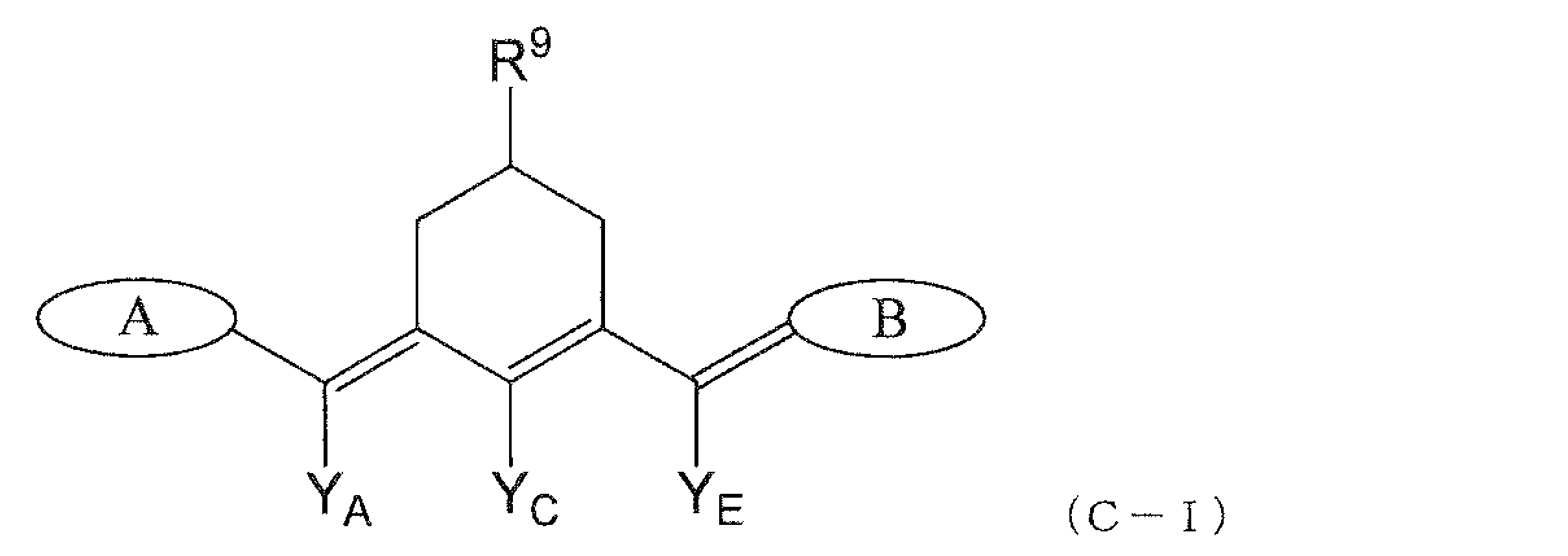


置換基R9としては、水素原子、水酸基、=O、メチル基、エチル基、n-プロピル基、イソプロピル基、n-ブチル基、sec-ブチル基、tert-ブチル基、シクロヘキシル基が好ましく、水素原子、水酸基、=O、メチル基、エチル基、tert-ブチル基がより好ましい。 The substituent R 9 is preferably a hydrogen atom, a hydroxyl group, ═O, a methyl group, an ethyl group, an n-propyl group, an isopropyl group, an n-butyl group, a sec-butyl group, a tert-butyl group, or a cyclohexyl group, and more preferably a hydrogen atom, a hydroxyl group, ═O, a methyl group, an ethyl group, or a tert-butyl group.
前記YA、YCおよびYEはそれぞれ独立に、より好ましくは、水素原子、塩素原子、臭素原子、フッ素原子、水酸基、フェニルアミノ基(NHPh)、ジフェニルアミノ基、メチルフェニルアミノ基、ジメチルアミノ基、メチル基、メトキシ基、フェニル基、フェノキシ基、4-メチルフェノキシ基、メチルチオ基、フェニルチオ基、-S-(4-tolyl)基である。 More preferably, Y , YC and YE are each independently a hydrogen atom, a chlorine atom, a bromine atom, a fluorine atom, a hydroxyl group, a phenylamino group (NHPh), a diphenylamino group, a methylphenylamino group, a dimethylamino group, a methyl group, a methoxy group, a phenyl group, a phenoxy group, a 4-methylphenoxy group, a methylthio group, a phenylthio group, or an -S-(4-tolyl) group.
前記Laは、好ましくは、メチル基(Me)、エチル基(Et)、n-プロピル基、イソプロピル基(i-Pr)、n-ブチル基、sec-ブチル基、tert-ブチル基(tert-Bu)、ペンチル基、ヘキシル基、オクチル基、ノニル基、デシル基、ドデシル基であり、より好ましくは、メチル基、エチル基、n-プロピル基、イソプロピル基、n-ブチル基、sec-ブチル基、tert-ブチル基である。 The L a is preferably a methyl group (Me), an ethyl group (Et), an n-propyl group, an isopropyl group (i-Pr), an n-butyl group, a sec-butyl group, a tert-butyl group (tert-Bu), a pentyl group, a hexyl group, an octyl group, a nonyl group, a decyl group, or a dodecyl group, and more preferably a methyl group, an ethyl group, an n-propyl group, an isopropyl group, an n-butyl group, a sec-butyl group, or a tert-butyl group.
前記Laは、ビニル基、1-プロペニル基、2-プロペニル基、ブテニル基、1,3-ブタジエニル基、2-メチル-1-プロペニル基、2-ペンテニル基、ヘキセニル基等のアルケニル基;エチニル基、プロピニル基、ブチニル基、2-メチル-1-プロピニル基、ヘキシニル基等のアルキニル基であってもよい。 The L a may be an alkenyl group such as a vinyl group, a 1-propenyl group, a 2-propenyl group, a butenyl group, a 1,3-butadienyl group, a 2-methyl-1-propenyl group, a 2-pentenyl group, or a hexenyl group; or an alkynyl group such as an ethynyl group, a propynyl group, a butynyl group, a 2-methyl-1-propynyl group, or a hexynyl group.
前記Lbにおける炭素数1~15のハロゲン置換アルキル基としては、例えば、炭素数1~15のアルキル基の少なくとも1つの水素原子がハロゲン原子で置換された基が挙げられ、好ましくは、トリクロロメチル基、トリフルオロメチル基、1,1-ジクロロエチル基、ペンタクロロエチル基、ペンタフルオロエチル基、ヘプタクロロプロピル基、ヘプタフルオロプロピル基である。 Examples of the halogen-substituted alkyl group having 1 to 15 carbon atoms in L b include alkyl groups having 1 to 15 carbon atoms in which at least one hydrogen atom is substituted with a halogen atom, and preferred examples include a trichloromethyl group, a trifluoromethyl group, a 1,1-dichloroethyl group, a pentachloroethyl group, a pentafluoroethyl group, a heptachloropropyl group, and a heptafluoropropyl group.
前記Lcにおける置換基Kを有してもよい炭素数3~14の脂環式炭化水素基としては、好ましくは、シクロプロピル基、シクロプロピルメチル基、メチルシクロプロピル基、シクロブチル基、シクロペンチル基、シクロヘキシル基、メチルシクロヘキシル基、シクロヘプチル基およびシクロオクチル基等のシクロアルキル基;ノルボルナン基およびアダマンチル基等の多環脂環式基が挙げられる。 Preferred examples of the alicyclic hydrocarbon group having 3 to 14 carbon atoms in Lc which may have a substituent K include cycloalkyl groups such as a cyclopropyl group, a cyclopropylmethyl group, a methylcyclopropyl group, a cyclobutyl group, a cyclopentyl group, a cyclohexyl group, a methylcyclohexyl group, a cycloheptyl group, and a cyclooctyl group; and polycyclic alicyclic groups such as a norbornane group and an adamantyl group.
前記Ldにおける置換基Kを有してもよい炭素数6~14の芳香族炭化水素基としては、好ましくは、フェニル基、トリル基、キシリル基、メシチル基(トリメチルフェニル基)、クメニル基、ビス(トリフルオロメチル)フェニル基、1-ナフチル基、2-ナフチル基、アントラセニル基、フェナントリル基、ベンジル基(CH2Ph)である。 The aromatic hydrocarbon group having 6 to 14 carbon atoms which may have a substituent K in Ld is preferably a phenyl group, a tolyl group, a xylyl group, a mesityl group (trimethylphenyl group), a cumenyl group, a bis(trifluoromethyl)phenyl group, a 1-naphthyl group, a 2-naphthyl group, an anthracenyl group, a phenanthryl group, or a benzyl group ( CH2Ph ).
前記Leにおける置換基Kを有してもよい炭素数3~14の複素環基としては、好ましくは、フラン、チオフェン、ピロール、インドール、インドリン、インドレニン、ベンゾフラン、ベンゾチオフェン、モルホリン、ピリジンである。 The heterocyclic group having 3 to 14 carbon atoms which may have a substituent K in the above L e is preferably furan, thiophene, pyrrole, indole, indoline, indolenine, benzofuran, benzothiophene, morpholine, or pyridine.
前記Lfにおける-ORとしては、好ましくは、メトキシ基、エトキシ基、プロポキシ基、イソプロポキシ基、ブトキシ基、メトキシメチル基、メトキシエチル基、ペンチルオキシ基、ヘキシルオキシ基、オクチルオキシ基、フェノキシ基(OPh)、4-メチルフェノキシ基、シクロヘキシルオキシ基である。 Preferred examples of —OR in Lf include a methoxy group, an ethoxy group, a propoxy group, an isopropoxy group, a butoxy group, a methoxymethyl group, a methoxyethyl group, a pentyloxy group, a hexyloxy group, an octyloxy group, a phenoxy group (OPh), a 4-methylphenoxy group, and a cyclohexyloxy group.
前記Lgにおける置換基Lを有してもよい炭素数1~9のアシル基としては、好ましくは、アセチル基、プロピオニル基、ブチリル基、イソブチリル基、ベンゾイル基、4-プロピルベンゾイル基、トリフルオロメチルカルボニル基である。 The acyl group having 1 to 9 carbon atoms which may have a substituent L in Lg is preferably an acetyl group, a propionyl group, a butyryl group, an isobutyryl group, a benzoyl group, a 4-propylbenzoyl group, or a trifluoromethylcarbonyl group.
前記Lhにおける置換基Lを有してもよい炭素数1~9のアルコキシカルボニル基としては、好ましくは、メトキシカルボニル基、エトキシカルボニル基、プロポキシカルボニル基、イソプロポキシカルボニル基、ブトキシカルボニル基、2-トリフルオロメチルエトキシカルボニル基、2-フェニルエトキシカルボニル基である。 The alkoxycarbonyl group having 1 to 9 carbon atoms which may have a substituent L in L h is preferably a methoxycarbonyl group, an ethoxycarbonyl group, a propoxycarbonyl group, an isopropoxycarbonyl group, a butoxycarbonyl group, a 2-trifluoromethylethoxycarbonyl group, or a 2-phenylethoxycarbonyl group.
前記Xは、好ましくは、酸素原子、硫黄原子、-NR8-であり、特に好ましくは、酸素原子である。 The above X is preferably an oxygen atom, a sulfur atom, or --NR 8 --, and particularly preferably an oxygen atom.
式(II)や(IV)において、左右のユニットAおよびBは同一であっても異なってもよいが、同一であることが合成上容易であるため好ましい。
なお、ここで、ユニットAおよびBが同一である組み合わせは、式(A-I)と式(B-I)、式(A-II)と式(B-II)、式(A-III)と式(B-III)である。
In formula (II) or (IV), the left and right units A and B may be the same or different, but it is preferred that they are the same for ease of synthesis.
In addition, here, combinations in which the units A and B are the same are formula (AI) and formula (BI), formula (A-II) and formula (B-II), and formula (A-III) and formula (B-III).
前記R1~R6はそれぞれ独立に、好ましくは、水素原子、塩素原子、フッ素原子、臭素原子、メチル基、エチル基、n-プロピル基、イソプロピル基、n-ブチル基、sec-ブチル基、tert-ブチル基、1,1-ジメチルブチル基、シクロプロピル基、シクロプロピルメチル基、シクロヘキシル基、アダマンチル基、フェニル基、2,4,6-トリメチルフェニル基、3,5-ビス(トリフルオロメチル)フェニル基、水酸基、アミノ基、ジメチルアミノ基(NMe2)、ジエチルアミノ基(NEt2)、ジブチルアミノ基(N(n-Bu)2)、シアノ基、ニトロ基、アセチルアミノ基、プロピオニルアミノ基、N-メチルアセチルアミノ基、トリフルオロメタノイルアミノ基、ペンタフルオロエタノイルアミノ基、tert-ブタノイルアミノ基、シクロヘキシノイルアミノ基、n-ブチルスルホニル基、ベンジル基、ジフェニルメチル基、トリフルオロメチル基、ジフルオロメチル基、メトキシ基であり、より好ましくは水素原子、塩素原子、フッ素原子、臭素原子、メチル基、エチル基、n-プロピル基、イソプロピル基、n-ブチル基、sec-ブチル基、tert-ブチル基、シクロヘキシル基、フェニル基、アミノ基、ベンジル基、ジフェニルメチル基、トリフルオロメチル基、ジフルオロメチル基、メトキシ基である。 The R 1 to R 6 each independently represent preferably a hydrogen atom, a chlorine atom, a fluorine atom, a bromine atom, a methyl group, an ethyl group, a n-propyl group, an isopropyl group, a n-butyl group, a sec-butyl group, a tert-butyl group, a 1,1-dimethylbutyl group, a cyclopropyl group, a cyclopropylmethyl group, a cyclohexyl group, an adamantyl group, a phenyl group, a 2,4,6-trimethylphenyl group, a 3,5-bis(trifluoromethyl)phenyl group, a hydroxyl group, an amino group, a dimethylamino group (NMe 2 ), a diethylamino group (NEt 2 ), a dibutylamino group (N(n-Bu) 2 ), cyano group, nitro group, acetylamino group, propionylamino group, N-methylacetylamino group, trifluoromethanoylamino group, pentafluoroethanoylamino group, tert-butanoylamino group, cyclohexinoylamino group, n-butylsulfonyl group, benzyl group, diphenylmethyl group, trifluoromethyl group, difluoromethyl group, and methoxy group, and more preferably a hydrogen atom, a chlorine atom, a fluorine atom, a bromine atom, a methyl group, an ethyl group, n-propyl group, an isopropyl group, n-butyl group, sec-butyl group, tert-butyl group, cyclohexyl group, phenyl group, amino group, benzyl group, diphenylmethyl group, trifluoromethyl group, difluoromethyl group, and methoxy group.
前記R1~R6の少なくとも1つは、波長700~750nm付近、または、波長720~900nm付近における吸収極大での高い近赤外線カット性能と高い可視光透過性能とを有し、光学特性に優れ、熱や光に対して十分な耐性を有する化合物を容易に得ることができる等の点から、前記La、LcまたはLdであることが好ましい。なお、前記ユニットAが前記式(A-III)であり、前記ユニットBが前記式(B-III)である場合、「R1~R6の少なくとも1つがLa、LcまたはLdである」とは、「R1、R2、R4、R5の少なくとも1つがLa、LcまたはLdである」ことを意味する。 At least one of R 1 to R 6 is preferably L a , L c or L d from the viewpoints of easily obtaining a compound having high near-infrared cutting performance and high visible light transmission performance at an absorption maximum in the vicinity of wavelengths of 700 to 750 nm or wavelengths of 720 to 900 nm , excellent optical properties, and sufficient resistance to heat and light. When the unit A is formula (A-III) and the unit B is formula (B-III), "at least one of R 1 to R 6 is L a , L c or L d " means "at least one of R 1 , R 2 , R 4 and R 5 is L a , L c or L d ".
前記R8としては、好ましくは、水素原子、メチル基、エチル基、n-プロピル基、イソプロピル基、n-ブチル基、ベンジル基、n-ペンチル基、n-ヘキシル基、tert-ブチル基であり、より好ましくは水素原子、メチル基、エチル基、n-プロピル基、イソプロピル基、n-ブチル基、ベンジル基である。 The R 8 is preferably a hydrogen atom, a methyl group, an ethyl group, an n-propyl group, an isopropyl group, an n-butyl group, a benzyl group, an n-pentyl group, an n-hexyl group, or a tert-butyl group, and more preferably a hydrogen atom, a methyl group, an ethyl group, an n-propyl group, an isopropyl group, an n-butyl group, or a benzyl group.
前記An-としては、一価のアニオンであれば特に制限されないが、好ましくは、塩素イオン、臭素イオン、ヨウ素イオン、PF4 -、過塩素酸アニオン、トリストリフルオロメタンスルホニルメチドアニオン、テトラフルオロボレートアニオン、ヘキサフルオロリン酸アニオン、ビス(トリフルオロメタンスルホニル)イミドアニオン、トリフルオロメタンスルホン酸アニオン、テトラキス(ペンタフルオロフェニル)ボレートアニオン、テトラキス(3,5-ビス(トリフルオロメチル)フェニル)ボレートアニオンなどが挙げられ、より好ましくは、ビス(トリフルオロメタンスルホニル)イミドアニオン、トリフルオロメタンスルホン酸アニオン、トリストリフルオロメタンスルホニルメチドアニオン、テトラキス(ペンタフルオロフェニル)ボレートアニオン、テトラキス(3,5-ビス(トリフルオロメチル)フェニル)ボレートアニオンであり、耐熱性により優れる化合物(Z)を容易に得ることができる等の点から、さらに好ましくは、ビス(トリフルオロメタンスルホニル)イミドアニオン、トリストリフルオロメタンスルホニルメチドアニオン、テトラキス(ペンタフルオロフェニル)ボレートアニオン、テトラキス(3,5-ビス(トリフルオロメチル)フェニル)ボレートアニオンであり、特に好ましくはテトラキス(ペンタフルオロフェニル)ボレートアニオンである。 The An − is not particularly limited as long as it is a monovalent anion, but preferable examples thereof include a chloride ion, a bromide ion, an iodide ion, PF 4 − , a perchlorate anion, a tristrifluoromethanesulfonylmethide anion, a tetrafluoroborate anion, a hexafluorophosphate anion, a bis(trifluoromethanesulfonyl)imide anion, a trifluoromethanesulfonate anion, a tetrakis(pentafluorophenyl)borate anion, and a tetrakis(3,5-bis(trifluoromethyl)phenyl)borate anion, and more preferable examples thereof include a bis(trifluoromethanesulfonyl)imide anion, a trifluoromethanesulfonate anion, a tristrifluoromethanesulfonylmethide anion, and a tetrakis(3,5-bis(trifluoromethyl)phenyl)borate anion. Among these, the tetrakis(pentafluorophenyl)borate anion and the tetrakis(3,5-bis(trifluoromethyl)phenyl)borate anion are more preferable, and from the viewpoint of being able to easily obtain a compound (Z) having superior heat resistance, the bis(trifluoromethanesulfonyl)imide anion, the tristrifluoromethanesulfonylmethide anion, the tetrakis(pentafluorophenyl)borate anion and the tetrakis(3,5-bis(trifluoromethyl)phenyl)borate anion are more preferable, and the tetrakis(pentafluorophenyl)borate anion is particularly preferable.
式(I)や(III)で表される化合物の具体例としては、例えば、下記表1~4に記載の化合物(z-1)~(z-173)が挙げられる。
これらの化合物(Z)は、具体的には、例えば、下記実施例に記載の方法で合成することができる。
Specific examples of the compounds represented by formula (I) or (III) include compounds (z-1) to (z-173) shown in Tables 1 to 4 below.
Specifically, these compounds (Z) can be synthesized, for example, by the methods described in the following examples.


なお、表4のR3およびR4の欄における「C-1、C-2」は、前記式(A-I)および前記式(B-I)におけるR3とR4とが互いに結合し、炭素数6の芳香族炭化水素基を形成していることを意味し、具体的には、ユニットAおよびBに相当する部分が、下記式C-1およびC-2で表される構造であることを意味する。
また、表4のYA,YE、R1およびR5の欄における「D-1」は、YAと前記式(A-III)におけるR1、YEと前記式(B-III)におけるR5が互いに結合して、6員の脂環基を形成していることを意味し、具体的には、化合物(z-163)のカチオンが、下記式D-1で表されることを意味する。
In addition, "C-1, C-2" in the columns for R3 and R4 in Table 4 means that R3 and R4 in the formula (A-I) and the formula (B-I) are bonded to each other to form an aromatic hydrocarbon group having 6 carbon atoms, and specifically means that the portions corresponding to units A and B have structures represented by the following formulas C-1 and C-2.
In addition, "D-1" in the columns for Y , Y , R , and R in Table 4 means that Y and R in formula (A-III), and Y and R in formula (B-III) are bonded to each other to form a 6-membered alicyclic group, and specifically means that the cation of compound (z-163) is represented by the following formula D-1.
化合物(Z)は、有機溶剤可溶の化合物であることが好ましく、特にジクロロメタン可溶の化合物であることが好ましい。
ここで、有機溶剤可溶とは、25℃の有機溶剤100gに対し、化合物(Z)が0.1g以上溶解する場合のことをいう。
Compound (Z) is preferably a compound soluble in an organic solvent, and particularly preferably a compound soluble in dichloromethane.
Here, "soluble in an organic solvent" refers to the case where 0.1 g or more of compound (Z) dissolves in 100 g of an organic solvent at 25°C.
化合物(Z)は、下記要件(A)を満たす化合物であることが好ましい。
要件(A):化合物(Z)をジクロロメタンに溶解させた溶液を用いて測定される透過スペクトル(但し、該透過スペクトルは、吸収極大波長における透過率が10%となるスペクトルである。以下この透過スペクトルを「化合物(Z)の透過スペクトル」ともいう。)において、波長430~580nmにおける透過率の平均値が、好ましくは93%以上、より好ましくは95%以上である。該透過率の平均値は高い方が好ましいため、その上限は特に制限されず、100%であってもよい。
化合物(Z)がこの要件(A)を満たすと、カットしたい近赤外線領域の波長の光を十分にカットしながらも可視光透過率の低下をより抑制できる。
The compound (Z) is preferably a compound that satisfies the following requirement (A).
Requirement (A): In a transmission spectrum measured using a solution of compound (Z) dissolved in dichloromethane (wherein the transmission spectrum is a spectrum in which the transmittance at the absorption maximum wavelength is 10%. Hereinafter, this transmission spectrum will also be referred to as the "transmission spectrum of compound (Z)"), the average transmittance at wavelengths of 430 to 580 nm is preferably 93% or more, more preferably 95% or more. Since a higher average transmittance is preferable, the upper limit is not particularly limited and may be 100%.
When the compound (Z) satisfies the requirement (A), it is possible to sufficiently block light having a wavelength in the near infrared region that is desired to be blocked, while further suppressing a decrease in the visible light transmittance.
なお、本発明において、波長A~Bnmの平均透過率は、Anm以上Bnm以下の、1nm刻みの各波長における透過率を測定し、その透過率の合計を、測定した透過率の数(波長範囲、B-A+1)で除すことで算出した値である。 In the present invention, the average transmittance for wavelengths A to B nm is a value calculated by measuring the transmittance at each wavelength from A nm to B nm in 1 nm increments, and dividing the sum of the transmittances by the number of measured transmittances (wavelength range, B-A+1).
化合物(Z)は、下記要件(B-1)または(B-2)を満たす化合物であることが好ましい。
要件(B-1):化合物(Z)をジクロロメタンに溶解させた溶液を用いて測定される吸収スペクトルにおいて、好ましくは波長720~900nmの範囲、より好ましくは波長740~880nmの範囲、特に好ましくは波長740~860nmの範囲に極大値を有する。
化合物(Z)の吸収極大波長が前記範囲にあると、波長720~900nm付近の光の反射光を抑制することができ、フレアやゴーストの少ない良好な画像を与えることができる光学フィルターを容易に得ることができる。
前記要件(B-1)を満たす化合物(Z)の好適例としては、前記ユニットAが、前記式(A-I)~(A-II)のいずれかであり、前記ユニットBが、前記式(B-I)~(B-II)のいずれかである化合物が挙げられる。
The compound (Z) is preferably a compound that satisfies the following requirement (B-1) or (B-2).
Requirement (B-1): In an absorption spectrum measured using a solution obtained by dissolving compound (Z) in dichloromethane, the compound (Z) has a maximum value preferably in the wavelength range of 720 to 900 nm, more preferably in the wavelength range of 740 to 880 nm, and particularly preferably in the wavelength range of 740 to 860 nm.
When the absorption maximum wavelength of the compound (Z) is within the above range, it is possible to easily obtain an optical filter that can suppress reflected light having a wavelength of about 720 to 900 nm and can give a good image with little flare or ghost.
Suitable examples of the compound (Z) satisfying the requirement (B-1) include compounds in which the unit A is any one of the formulas (AI) to (A-II) and the unit B is any one of the formulas (BI) to (B-II).
要件(B-2):化合物(Z)をジクロロメタンに溶解させた溶液を用いて測定される吸収スペクトルにおいて、好ましくは波長700~750nmの範囲、より好ましくは波長705~748nmの範囲、特に好ましくは波長710~745nmの範囲に極大値を有する。
化合物(Z)の吸収極大波長が前記範囲にあると、波長700~750nm付近の光の反射光を抑制することができ、フレアやゴーストの少ない良好な画像を与えることができる光学フィルターを容易に得ることができる。
前記要件(B-2)を満たす化合物(Z)の好適例としては、前記ユニットAが、前記式(A-III)であり、前記ユニットBが、前記式(B-III)である化合物が挙げられる。
Requirement (B-2): In an absorption spectrum measured using a solution obtained by dissolving compound (Z) in dichloromethane, the maximum value is preferably in the wavelength range of 700 to 750 nm, more preferably in the wavelength range of 705 to 748 nm, and particularly preferably in the wavelength range of 710 to 745 nm.
When the absorption maximum wavelength of the compound (Z) is within the above range, it is possible to easily obtain an optical filter that can suppress reflected light having a wavelength of about 700 to 750 nm and can give a good image with little flare or ghost.
Suitable examples of the compound (Z) satisfying the requirement (B-2) include compounds in which the unit A is represented by the formula (A-III) and the unit B is represented by the formula (B-III).
化合物(Z)は、下記要件(C)を満たす化合物であることが好ましい。
要件(C):樹脂と化合物(Z)とからなる樹脂板の、波長700~1000nmの範囲の極大吸収波長λaにおける吸光度Aiに対する、該樹脂板を30日間蛍光灯照射した後の前記λaおける吸光度Afの保持率D(=Af×100/Ai)が、好ましくは95%以上、より好ましくは97%以上である。該保持率Dは高い方が好ましいため、その上限は特に制限されず、100%であってもよい。
なお、前記樹脂板の厚みは、90~110μmの範囲内であり、樹脂に対する化合物(Z)の含有量は、該樹脂板の極大吸収波長λaにおける吸光度Aiが0.5~1.5の範囲内に入るような量であり、樹脂は、JSR(株)製アートンを使用するものとし、樹脂板中の樹脂100質量部に対して、Irganox 1010(BASFジャパン(株)製)を0.3質量部含むものとする。
The compound (Z) is preferably a compound that satisfies the following requirement (C).
Requirement (C): The retention rate D (=Af×100/Ai) of absorbance Af at a maximum absorption wavelength λa in the wavelength range of 700 to 1000 nm of a resin plate made of a resin and a compound (Z) after the resin plate is irradiated with a fluorescent lamp for 30 days relative to absorbance Ai at the maximum absorption wavelength λa is preferably 95% or more, more preferably 97% or more. Since the higher the retention rate D, the better, there is no particular restriction on the upper limit, and it may be 100%.
The thickness of the resin plate is within a range of 90 to 110 μm, the content of the compound (Z) relative to the resin is an amount such that the absorbance Ai at the maximum absorption wavelength λa of the resin plate is within a range of 0.5 to 1.5, and the resin used is Arton manufactured by JSR Corporation, and contains 0.3 parts by mass of Irganox 1010 (manufactured by BASF Japan Ltd.) relative to 100 parts by mass of the resin in the resin plate.
保持率Dが前記範囲にある化合物(Z)は、耐光性(耐久性)に優れるといえ、このような化合物(Z)を用いることで、長期にわたり所望の光学特性を示す光学フィルターを容易に得ることができる。
前記保持率Dは、具体的には、下記実施例に記載の方法で測定することができる。
The compound (Z) having a retention rate D within the above range can be said to have excellent light resistance (durability), and by using such a compound (Z), an optical filter exhibiting desired optical properties over a long period of time can be easily obtained.
Specifically, the retention rate D can be measured by the method described in the following examples.
化合物(Z)は、下記要件(D)を満たすことがより好ましい。
要件(D):化合物(Z)をジクロロメタンに溶解させた溶液を用いて測定される分光吸収スペクトルにおいて、極大吸収波長のうち、最も長い波長における吸光度をεa、波長430~580nmにおける吸光度の最大値をεbmaxとした時、εa/εbmaxが、好ましくは20以上、より好ましくは25以上、さらに好ましくは27以上である。εa/εbmaxは、大きい方が好ましいためその上限は特に制限されないが、例えば、10000以下である。
化合物(Z)がこの要件(D)を満たすと、可視光域の吸光度に対する赤外線域の吸光度の比が大きいといえ、光学特性に優れるといえ、誘電体多層膜を有する光学フィルターにおいて、該多層膜による入射角依存性を抑制することができる。
It is more preferable that the compound (Z) satisfies the following requirement (D).
Requirement (D): In a spectroscopic absorption spectrum measured using a solution obtained by dissolving compound (Z) in dichloromethane, when the absorbance at the longest wavelength among the maximum absorption wavelengths is εa and the maximum absorbance at wavelengths of 430 to 580 nm is εbmax, εa/εbmax is preferably 20 or more, more preferably 25 or more, and even more preferably 27 or more. Since a larger εa/εbmax is preferable, the upper limit is not particularly limited, but is, for example, 10,000 or less.
When compound (Z) satisfies requirement (D), it can be said that the ratio of absorbance in the infrared region to the absorbance in the visible light region is large, and the optical properties are excellent. In an optical filter having a dielectric multilayer film, the incidence angle dependency due to the multilayer film can be suppressed.
本組成物中の化合物(Z)の含有量は、樹脂100質量部に対して、好ましくは0.02~2.0質量部、より好ましくは0.02~1.5質量部、特に好ましくは0.03~1.5質量部である。
化合物(Z)の含有量が前記範囲にあると、波長700~750nm付近、または、波長720~900nm付近の範囲の近赤外線を効率よくカットできるほか、可視光透過性により優れる組成物を容易に得ることができる。
The content of compound (Z) in the present composition is preferably 0.02 to 2.0 parts by mass, more preferably 0.02 to 1.5 parts by mass, and particularly preferably 0.03 to 1.5 parts by mass, per 100 parts by mass of the resin.
When the content of compound (Z) is within the above range, near-infrared rays having a wavelength of about 700 to 750 nm or about 720 to 900 nm can be efficiently cut, and a composition having excellent visible light transmittance can be easily obtained.
<樹脂>
本組成物に用いる樹脂としては特に制限されず、従来公知の樹脂を用いることができる。
本組成物に用いられる樹脂は、1種単独でもよく、2種以上でもよい。
<Resin>
The resin used in the present composition is not particularly limited, and any conventionally known resin can be used.
The resin used in the present composition may be one type alone or two or more types.
前記樹脂としては、本発明の効果を損なわない限り特に制限されないが、例えば、熱安定性およびフィルム(板)形状への成形性等に優れ、かつ、100℃以上程度の蒸着温度で行う高温蒸着で誘電体多層膜を形成し得るフィルムを容易に得ることができる等の点から、ガラス転移温度(Tg)が、好ましくは110~380℃、より好ましくは110~370℃、特に好ましくは120~360℃である樹脂が挙げられる。また、前記樹脂のTgが140℃以上であると、誘電体多層膜をより高温で蒸着形成し得るフィルムが得られるため、特に好ましい。 The resin is not particularly limited as long as it does not impair the effects of the present invention. For example, a resin having a glass transition temperature (Tg) of preferably 110 to 380°C, more preferably 110 to 370°C, and particularly preferably 120 to 360°C can be used, because it has excellent thermal stability and moldability into a film (plate) shape, and can easily produce a film that can form a dielectric multilayer film by high-temperature deposition at a deposition temperature of about 100°C or higher. In addition, a resin having a Tg of 140°C or higher is particularly preferred, because it can produce a film that can form a dielectric multilayer film by deposition at a higher temperature.
前記樹脂としては、当該樹脂からなる厚さ0.1mmの樹脂板の全光線透過率(JIS K 7375:2008)が、好ましくは75~95%、さらに好ましくは78~95%、特に好ましくは80~95%となる樹脂を用いることができる。
全光線透過率が前記範囲にある樹脂を用いると、透明性に優れる樹脂組成物や光学フィルターを容易に得ることができる。
The resin that can be used is one that has a total light transmittance (JIS K 7375:2008) of preferably 75 to 95%, more preferably 78 to 95%, and particularly preferably 80 to 95% when formed into a 0.1 mm-thick resin plate.
By using a resin having a total light transmittance within the above range, a resin composition or optical filter having excellent transparency can be easily obtained.
前記樹脂のゲルパーミエーションクロマトグラフィー(GPC)法により測定される、ポリスチレン換算の重量平均分子量(Mw)は、通常15,000~350,000、好ましくは30,000~250,000であり、数平均分子量(Mn)は、通常10,000~150,000、好ましくは20,000~100,000である。 The weight average molecular weight (Mw) of the resin, measured by gel permeation chromatography (GPC) in terms of polystyrene, is usually 15,000 to 350,000, preferably 30,000 to 250,000, and the number average molecular weight (Mn) is usually 10,000 to 150,000, preferably 20,000 to 100,000.
前記樹脂としては、例えば、環状(ポリ)オレフィン系樹脂、芳香族ポリエーテル系樹脂、ポリイミド系樹脂、ポリエステル系樹脂、ポリカーボネート系樹脂、ポリアミド(アラミド)系樹脂、ポリアリレート系樹脂、ポリサルホン系樹脂、ポリエーテルサルホン系樹脂、ポリパラフェニレン系樹脂、ポリアミドイミド系樹脂、ポリエチレンナフタレート(PEN)系樹脂、フッ素化芳香族ポリマー系樹脂、(変性)アクリル系樹脂、エポキシ系樹脂、アリルエステル系硬化型樹脂、シルセスキオキサン系紫外線硬化型樹脂、アクリル系紫外線硬化型樹脂、ビニル系紫外線硬化型樹脂が挙げられる。
これらの樹脂の具体例としては、国際公開第2019/168090号に記載の樹脂等が挙げられる。
Examples of the resin include cyclic (poly)olefin-based resins, aromatic polyether-based resins, polyimide-based resins, polyester-based resins, polycarbonate-based resins, polyamide (aramid)-based resins, polyarylate-based resins, polysulfone-based resins, polyethersulfone-based resins, polyparaphenylene-based resins, polyamideimide-based resins, polyethylene naphthalate (PEN)-based resins, fluorinated aromatic polymer-based resins, (modified) acrylic-based resins, epoxy-based resins, allyl ester-based curable resins, silsesquioxane-based ultraviolet-curable resins, acrylic-based ultraviolet-curable resins, and vinyl-based ultraviolet-curable resins.
Specific examples of these resins include the resins described in WO 2019/168090.
<その他成分>
本組成物は、本発明の効果を損なわない範囲において、さらに、化合物(Z)以外の化合物(X)[紫外線吸収剤以外の吸収剤]、酸化防止剤、紫外線吸収剤、蛍光消光剤および金属錯体系化合物等のその他成分を含有してもよい。
これらその他成分はそれぞれ、1種単独で用いてもよく、2種以上を用いてもよい。
<Other ingredients>
The present composition may further contain other components, such as a compound (X) other than the compound (Z) [an absorber other than an ultraviolet absorber], an antioxidant, an ultraviolet absorber, a fluorescence quencher, and a metal complex compound, within the scope of not impairing the effects of the present invention.
Each of these other components may be used alone or in combination of two or more.
これらその他成分は、本組成物を調製する際に、樹脂などとともに混合してもよいし、樹脂を合成する際に添加してもよい。また、添加量は、所望の特性等に応じて適宜選択すればよいが、樹脂100質量部に対して、通常0.01~5.0質量部、好ましくは0.05~2.0質量部である。 These other components may be mixed with the resin when preparing the composition, or may be added when synthesizing the resin. The amount added may be appropriately selected depending on the desired properties, but is usually 0.01 to 5.0 parts by mass, and preferably 0.05 to 2.0 parts by mass, per 100 parts by mass of resin.
[化合物(X)]
本組成物は、化合物(Z)以外の化合物(X)[紫外線吸収剤以外の吸収剤]を1種または2種以上含んでいてもよい。
該化合物(X)としては、例えば、スクアリリウム系化合物、フタロシアニン系化合物、ポリメチン系化合物、ナフタロシアニン系化合物、クロコニウム系化合物、オクタフィリン系化合物、ジイモニウム系化合物、ペリレン系化合物、金属ジチオラート系化合物が挙げられる。
[Compound (X)]
The present composition may contain one or more compounds (X) [absorbing agents other than ultraviolet absorbents] other than the compound (Z).
Examples of the compound (X) include squarylium-based compounds, phthalocyanine-based compounds, polymethine-based compounds, naphthalocyanine-based compounds, croconium-based compounds, octaphylline-based compounds, diimonium-based compounds, perylene-based compounds, and metal dithiolate-based compounds.
前記化合物(X)としては、スクアリリウム系化合物を含むことが好ましく、スクアリリウム系化合物とその他の化合物(X')とをそれぞれ1種以上含むことがさらに好ましく、該その他の化合物(X')としては、フタロシアニン系化合物およびポリメチン系化合物が特に好ましい。 The compound (X) preferably includes a squarylium-based compound, and more preferably includes at least one squarylium-based compound and at least one other compound (X'). As the other compound (X'), a phthalocyanine-based compound and a polymethine-based compound are particularly preferred.
前記スクアリリウム系化合物は、吸収ピークがシャープであり、優れた可視光透過性および高いモル吸光係数を有するが、光線吸収時に散乱光の原因となる蛍光が発生する場合がある。この場合、スクアリリウム系化合物と前記化合物(X')とを組み合わせて使用することにより、散乱光を抑制することができる。このように散乱光が抑制されると、本組成物から得られた光学フィルターを撮像装置などに使用した場合、得られるカメラ画質がより良好となる。 The squarylium-based compound has a sharp absorption peak, excellent visible light transmittance, and a high molar extinction coefficient, but may generate fluorescence that causes scattered light when absorbing light. In this case, the scattered light can be suppressed by using a squarylium-based compound in combination with the compound (X'). When the scattered light is suppressed in this way, the camera image quality obtained is better when an optical filter obtained from this composition is used in an imaging device or the like.
前記化合物(X)の吸収極大波長は、好ましくは650~1100nm、より好ましくは650~950nm、さらに好ましくは680~850nm、特に好ましくは690~740nmである。
前記範囲に吸収極大波長を有する化合物(X)を用いることで、視感度補正により優れる光学フィルターを容易に得ることができる。
The absorption maximum wavelength of the compound (X) is preferably 650 to 1100 nm, more preferably 650 to 950 nm, further preferably 680 to 850 nm, and particularly preferably 690 to 740 nm.
By using the compound (X) having a maximum absorption wavelength within the above range, an optical filter having excellent visibility correction can be easily obtained.
[紫外線吸収剤]
前記紫外線吸収剤としては、例えば、アゾメチン系化合物、インドール系化合物、ベンゾトリアゾール系化合物、シアノアクリレート系化合物、トリアジン系化合物、アントラセン系化合物、特開2019-014707号公報等に記載の化合物が挙げられる。
[Ultraviolet absorber]
Examples of the ultraviolet absorber include azomethine compounds, indole compounds, benzotriazole compounds, cyanoacrylate compounds, triazine compounds, anthracene compounds, and compounds described in JP-A-2019-014707.
特にアゾメチン系化合物、インドール系化合物、ベンゾトリアゾール系化合物、シアノアクリレート系化合物が好ましい。これら化合物を含有することで、近紫外波長領域においても入射角度依存性が少ない光学フィルターを容易に得ることができ、該光学フィルターを撮像装置などに使用した場合、得られるカメラ画質がより良好となる。 Azomethine compounds, indole compounds, benzotriazole compounds, and cyanoacrylate compounds are particularly preferred. By including these compounds, an optical filter that has little incidence angle dependency even in the near-ultraviolet wavelength region can be easily obtained, and when the optical filter is used in an imaging device or the like, the resulting camera image quality is better.
[酸化防止剤]
前記酸化防止剤としては、例えば、2,6-ジ-tert-ブチル-4-メチルフェノール、2,2'-ジオキシ-3,3'-ジ-tert-ブチル-5,5'-ジメチルジフェニルメタン、テトラキス[メチレン-3-(3,5-ジ-tert-ブチル-4-ヒドロキシフェニル)プロピオネート]メタンが挙げられる。
[Antioxidants]
Examples of the antioxidant include 2,6-di-tert-butyl-4-methylphenol, 2,2'-dioxy-3,3'-di-tert-butyl-5,5'-dimethyldiphenylmethane, and tetrakis[methylene-3-(3,5-di-tert-butyl-4-hydroxyphenyl)propionate]methane.
<添加剤>
本組成物は、本発明の効果を損なわない範囲において、さらに、有機溶剤、離型剤、界面活性剤、帯電防止剤、密着助剤、光拡散材等の添加剤を含有していてもよい。
これら添加剤はそれぞれ、1種単独で用いてもよく、2種以上を用いてもよい。
<Additives>
The present composition may further contain additives such as an organic solvent, a release agent, a surfactant, an antistatic agent, an adhesion aid, and a light diffusing material, provided the effects of the present invention are not impaired.
Each of these additives may be used alone or in combination of two or more.
特に、本組成物を液状組成物とする場合、有機溶剤を用いることが好ましい。該有機溶剤の例としては、樹脂を溶解できる溶剤であることが好ましく、具体的には、エステル類、ケトン類、芳香族炭化水素類、ハロゲン含有化合物類が挙げられる。
また、後述するキャスト成形により樹脂層を製造する場合には、レベリング剤や消泡剤を用いることで該樹脂層の製造を容易にすることができる。
In particular, when the present composition is made into a liquid composition, it is preferable to use an organic solvent. Examples of the organic solvent are preferably solvents capable of dissolving resins, and specific examples thereof include esters, ketones, aromatic hydrocarbons, and halogen-containing compounds.
Furthermore, when the resin layer is produced by cast molding, which will be described later, the production of the resin layer can be facilitated by using a leveling agent or an antifoaming agent.
≪基材(i)≫
本発明に係る基材(i)は、本組成物から形成された前記化合物(Z)を含有する基材である。
該基材(i)は、単層であっても多層であってもよく、本組成物から形成された前記化合物(Z)を含有する樹脂層(以下「本樹脂層」ともいう。)を有すればよい。前記基材(i)は、2層以上の本樹脂層を有していてもよく、この場合、2層以上の本樹脂層は、同一であっても、異なっていてもよい。
<<Substrate (i)>>
The substrate (i) according to the present invention is a substrate containing the compound (Z) formed from the present composition.
The substrate (i) may be a single layer or a multilayer, and may have a resin layer (hereinafter also referred to as the present resin layer) containing the compound (Z) formed from the present composition. The substrate (i) may have two or more present resin layers, and in this case, the two or more present resin layers may be the same or different.
基材(i)が単層の場合は、該基材(i)は本樹脂層からなり、つまり、本樹脂層(樹脂製基板)が基材(i)である。
基材(i)が多層の場合は、該基材(i)としては、2層以上の樹脂層を含む基材であって、該2層以上の樹脂層のうち少なくとも1つが本樹脂層である基材や、本樹脂層とガラス支持体とを含む基材が挙げられ、好適例としては、ガラス支持体やベースとなる樹脂製支持体などの支持体上に本樹脂層が積層された積層体を含む基材(A)、本樹脂層上に、硬化性樹脂等からなるオーバーコート層などの樹脂層が積層された積層体を含む基材(B)が挙げられる。
製造コストや光学特性調整の容易性、さらに、本樹脂層の傷消し効果を達成できることや、基材(i)の耐傷つき性向上等の点から、前記基材(i)としては、基材(B)が特に好ましい。
When the substrate (i) is a single layer, the substrate (i) is composed of the present resin layer, that is, the present resin layer (resin substrate) is the substrate (i).
When the substrate (i) is a multilayer substrate, examples of the substrate (i) include a substrate including two or more resin layers, at least one of which is the present resin layer, and a substrate including the present resin layer and a glass support. Suitable examples include a substrate (A) including a laminate in which the present resin layer is laminated on a support such as a glass support or a base resin support, and a substrate (B) including a laminate in which a resin layer such as an overcoat layer made of a curable resin or the like is laminated on the present resin layer.
From the viewpoints of production costs, ease of adjusting optical properties, ability to achieve the scratch-eliminating effect of the resin layer, and improvement of scratch resistance of the substrate (i), the substrate (B) is particularly preferred as the substrate (i).
なお、前記樹脂製支持体や基材(B)におけるオーバーコート層などの樹脂層は、化合物(Z)を含まない樹脂層のことをいう。該化合物(Z)を含まない樹脂層は、樹脂を含めば特に制限されず、該樹脂としては、前記本組成物の欄に記載の樹脂と同様の樹脂等が挙げられる。また、該化合物(Z)を含まない樹脂層は、下記その他の機能膜であってもよい。 The resin layer such as the overcoat layer in the resin support or substrate (B) refers to a resin layer that does not contain the compound (Z). The resin layer that does not contain the compound (Z) is not particularly limited as long as it contains a resin, and examples of the resin include the same resins as those described in the section on the present composition. The resin layer that does not contain the compound (Z) may also be any of the other functional films described below.
前記ガラス支持体としては透明ガラス支持体や吸収ガラス支持体が好ましい。これらの中でも、吸収ガラス支持体を用いると近赤外線領域の波長の光を十分にカットすることができるため、好ましい。 As the glass support, a transparent glass support or an absorbing glass support is preferable. Among these, the use of an absorbing glass support is preferable because it can sufficiently cut light with wavelengths in the near infrared region.
基材(i)の厚みは、所望の用途に応じて適宜選択することができ、特に制限されないが、好ましくは10~250μm、さらに好ましくは15~230μm、特に好ましくは20~150μmである。
基材(i)の厚みが前記範囲にあると、該基材(i)を用いた光学フィルターを薄型化および軽量化することができ、固体撮像装置等の様々な用途に好適に用いることができる。特に、前記単層の基材(i)をカメラモジュール等のレンズユニットに用いた場合には、レンズユニットの低背化、軽量化を実現することができるため好ましい。
The thickness of the substrate (i) can be appropriately selected depending on the desired application and is not particularly limited, but is preferably 10 to 250 μm, more preferably 15 to 230 μm, and particularly preferably 20 to 150 μm.
When the thickness of the substrate (i) is within the above range, the optical filter using the substrate (i) can be made thin and lightweight, and can be suitably used for various applications such as solid-state imaging devices, etc. In particular, when the single-layer substrate (i) is used in a lens unit of a camera module or the like, it is preferable because the lens unit can be made low-profile and lightweight.
[基材(i)の製造方法]
前記本樹脂層、前記樹脂製支持体および前記オーバーコート層などの樹脂層は、例えば、溶融成形またはキャスト成形により形成することができ、さらに、必要により、成形後に、反射防止剤、ハードコート剤および/または帯電防止剤等のコーティング剤をコーティングしてもよい。
[Method for producing substrate (i)]
The resin layer, the resin support, and the resin layer such as the overcoat layer can be formed, for example, by melt molding or cast molding, and further, if necessary, after molding, a coating agent such as an antireflection agent, a hard coat agent, and/or an antistatic agent may be coated.
前記基材(i)が、基材(A)である場合、例えば、前記支持体に、本組成物を溶融成形またはキャスト成形することで、好ましくはスピンコート、スリットコート、インクジェットなどの方法にて塗工した後に溶媒を乾燥除去し、必要に応じてさらに光照射や加熱を行うことで、支持体上に本樹脂層が形成された基材を製造することができる。 When the substrate (i) is substrate (A), for example, the composition is melt-molded or cast-molded onto the substrate, preferably by spin coating, slit coating, inkjet or other methods, and the solvent is then dried and removed, and further light irradiation or heating is performed as necessary, thereby producing a substrate having the resin layer formed on the substrate.
・溶融成形
前記溶融成形としては、具体的には、本組成物を溶融混練りして得られたペレットを溶融成形する方法;本組成物を溶融成形する方法;溶剤を含む液状の本組成物から溶剤を除去して得られたペレットを溶融成形する方法などが挙げられる。溶融成形方法としては、射出成形、溶融押出成形またはブロー成形などを挙げることができる。
- Melt molding Specific examples of the melt molding include a method of melt-kneading the present composition to obtain pellets, a method of melt molding the present composition, a method of removing the solvent from the present composition in a liquid state containing the solvent and melt molding the pellets, etc. Examples of the melt molding method include injection molding, melt extrusion molding, blow molding, etc.
・キャスト成形
前記キャスト成形としては、溶剤を含む液状の本組成物を適当な支持体の上にキャスティングして溶剤を除去する方法;前記樹脂として光硬化性樹脂および/または熱硬化性樹脂を含む、硬化性の本組成物を適当な支持体の上にキャスティングして溶媒を除去した後、紫外線照射や加熱などの適切な手法により硬化させる方法などが挙げられる。
前記基材(i)が、前記単層の基材(i)である場合には、該基材(i)は、キャスト成形後、支持体から塗膜を剥離することにより得ることができ、また、前記基材(i)が、前記基材(A)である場合には、該基材(i)は、キャスト成形後、塗膜を剥離しないことで得ることができる。
Cast molding Examples of the cast molding include a method in which a liquid present composition containing a solvent is cast onto a suitable support and the solvent is removed; and a method in which a curable present composition containing a photocurable resin and/or a thermosetting resin as the resin is cast onto a suitable support and the solvent is removed, followed by curing by a suitable method such as ultraviolet irradiation or heating.
When the substrate (i) is the substrate (i) having a single layer, the substrate (i) can be obtained by peeling off the coating film from the support after cast molding, and when the substrate (i) is the substrate (A), the substrate (i) can be obtained by not peeling off the coating film after cast molding.
前記適当な支持体としては、例えば、ガラス板、スチールベルト、スチールドラムおよび樹脂(例えば、ポリエステルフィルム、環状オレフィン系樹脂フィルム)製支持体が挙げられる。 Examples of suitable supports include glass plates, steel belts, steel drums, and resin (e.g., polyester films, cyclic olefin resin films) supports.
さらに、ガラス板、石英またはプラスチック製等の光学部品に、前記液状の本組成物をコーティングして溶剤を乾燥させる方法、または、前記硬化性の本組成物をコーティングして硬化および乾燥させる方法などにより、光学部品上に本樹脂層を形成することもできる。 Furthermore, the resin layer can be formed on an optical component such as a glass plate, quartz, or plastic by coating the liquid composition and drying the solvent, or by coating the curable composition and curing and drying it.
前記樹脂製支持体およびオーバーコート層などの樹脂層を溶融成形またはキャスト成形により形成する場合には、前記溶融成形やキャスト成形の欄における本組成物の代わりに、樹脂を含む所望の組成物(但し、化合物(Z)を含まない)を用いればよい。 When the resin support and the resin layer such as the overcoat layer are formed by melt molding or cast molding, a desired composition containing a resin (but not containing compound (Z)) may be used in place of the present composition in the melt molding or cast molding section.
前記本樹脂層、前記樹脂製支持体および前記オーバーコート層などの樹脂層中の残留溶剤量は可能な限り少ない方がよい。具体的には、該残留溶剤量は、本樹脂層の重さに対して、好ましくは3質量%以下、より好ましくは1質量%以下、さらに好ましくは0.5質量%以下である。
残留溶剤量が前記範囲にあると、変形や特性が変化しにくい、所望の機能を容易に発揮できる樹脂層が得られる。
基材(i)を光学フィルターに用いる場合は、前記本樹脂層、前記樹脂製支持体および前記オーバーコート層などの樹脂層中の溶剤含有量を100質量ppm以下に抑えることが好ましい。
The amount of residual solvent in the resin layer, the resin support, the overcoat layer, and other resin layers is preferably as small as possible. Specifically, the amount of residual solvent is preferably 3% by mass or less, more preferably 1% by mass or less, and even more preferably 0.5% by mass or less, based on the weight of the resin layer.
When the amount of the residual solvent is within the above range, a resin layer that is resistant to deformation and changes in properties and can easily exhibit the desired functions can be obtained.
When the substrate (i) is used in an optical filter, it is preferable to suppress the solvent content in the resin layers, such as the present resin layer, the resin support and the overcoat layer, to 100 ppm by mass or less.
≪光学フィルター≫
本発明に係る光学フィルター(以下「本フィルター」ともいう。)は、前記基材(i)と、誘電体多層膜とを有する。
本発明の効果がより発揮される等の点から、このような本フィルターとしては、具体的には、近赤外線カットフィルター(NIR-CF)、可視光-近赤外線選択透過フィルター(DBPF)、近赤外線透過フィルター(IRPF)が挙げられる。また、本フィルターは、科学捜査等に用いられる代替光源(ALS:Alternative Light Sources)用のフィルターとしても用いることができる。これらのフィルターは、前記基材(i)を有する以外は、従来公知の構成とすればよい。
Optical Filter
The optical filter according to the present invention (hereinafter also referred to as "the present filter") comprises the above-mentioned substrate (i) and a dielectric multilayer film.
From the viewpoint of more effectively exerting the effects of the present invention, specific examples of such a filter include a near-infrared cut filter (NIR-CF), a visible light-near-infrared selective transmission filter (DBPF), and a near-infrared transmission filter (IRPF). The filter can also be used as a filter for alternative light sources (ALS: Alternative Light Sources) used in scientific investigations and the like. These filters may have a conventionally known configuration except that they have the base material (i).
本フィルターが、NIR-CFやDBPFである場合、下記特性(a)を満たすフィルターであることが好ましい。
特性(a):波長430~580nmの領域において、光学フィルターの垂直方向から測定した場合の透過率の平均値が、好ましくは75%以上、より好ましくは80%以上である。該透過率の平均値は高い方が好ましいため、その上限は特に制限されず、100%であってもよい。
本フィルターがこの特性(a)を満たすと、カットしたい近赤外線領域の波長の光を十分にカットしながらも可視光透過率の低下をより抑制できるため、NIR-CFやDBPFとしてより好適に用いることができる。
When the present filter is an NIR-CF or DBPF, it is preferable that the filter satisfies the following characteristic (a).
Property (a): In the wavelength region of 430 to 580 nm, the average transmittance measured from the perpendicular direction of the optical filter is preferably 75% or more, more preferably 80% or more. Since a higher average transmittance is preferable, the upper limit is not particularly limited and may be 100%.
When the present filter satisfies the characteristic (a), it is possible to suppress the decrease in visible light transmittance while sufficiently cutting light of wavelengths in the near-infrared region that are to be cut, and therefore it can be more suitably used as an NIR-CF or DBPF.
前記基材(i)が、前記要件(B-1)を満たす化合物を含む場合であって、本フィルターが、NIR-CFやDBPFである場合、下記特性(b-1)を満たすフィルターであることが好ましい。
特性(b-1):波長700~800nmの領域において、光学フィルターの少なくとも一方の面の垂直方向から5°の角度から入射する無偏光光線の平均反射率が、好ましくは25%以下、より好ましくは15%以下である。該平均反射率は低い方が好ましいため、その下限は特に制限されず、0%であってもよい。
この特性(b-1)を満たす本フィルターを用いることで、波長700~800nmの波長域の反射光強度の低減が可能であるため、該反射光に起因する画像不良を解消できる。
When the base material (i) contains a compound satisfying the requirement (B-1) and the present filter is an NIR-CF or DBPF, the filter preferably satisfies the following characteristic (b-1):
Property (b-1): In the wavelength region of 700 to 800 nm, the average reflectance of unpolarized light incident at an angle of 5° from the perpendicular direction to at least one surface of the optical filter is preferably 25% or less, more preferably 15% or less. Since a lower average reflectance is preferable, the lower limit is not particularly limited and may be 0%.
By using the present filter which satisfies the characteristic (b-1), it is possible to reduce the intensity of reflected light in the wavelength region of 700 to 800 nm, thereby eliminating image defects caused by the reflected light.
前記基材(i)が、前記要件(B-2)を満たす化合物を含む場合であって、本フィルターが、NIR-CFやDBPFである場合、下記特性(b-2)を満たすフィルターであることが好ましい。
特性(b-2):波長650~800nmの領域において、光学フィルターの少なくとも一方の面の垂直方向から5°の角度から入射する無偏光光線の平均反射率が、好ましくは25%以下、より好ましくは15%以下である。該平均反射率は低い方が好ましいため、その下限は特に制限されず、0%であってもよい。
この特性(b-2)を満たす本フィルターを用いることで、波長650~800nmの波長域の反射光強度の低減が可能であるため、該反射光に起因する画像不良を解消できる。
When the base material (i) contains a compound satisfying the requirement (B-2) and the present filter is an NIR-CF or DBPF, the filter preferably satisfies the following characteristic (b-2).
Characteristic (b-2): In the wavelength region of 650 to 800 nm, the average reflectance of unpolarized light incident at an angle of 5° from the perpendicular direction to at least one surface of the optical filter is preferably 25% or less, more preferably 15% or less. Since a lower average reflectance is preferable, the lower limit is not particularly limited and may be 0%.
By using the present filter which satisfies the characteristic (b-2), it is possible to reduce the intensity of reflected light in the wavelength region of 650 to 800 nm, thereby eliminating image defects caused by the reflected light.
なお、本発明において、波長A~Bnmの平均反射率は、Anm以上Bnm以下の、1nm刻みの各波長における反射率を測定し、その反射率の合計を、測定した反射率の数(波長範囲、B-A+1)で除すことで算出した値である。
垂直方向から入射する無偏光光線の反射率を測定することは、限りなく困難であるため、本発明では、垂直方向から5°の角度から入射する無偏光光線の反射特性を測定した。
In the present invention, the average reflectance for wavelengths A to B nm is a value calculated by measuring the reflectance at each wavelength in 1 nm increments from A nm to B nm, and dividing the sum of the reflectances by the number of measured reflectances (wavelength range, B-A+1).
Since it is extremely difficult to measure the reflectance of unpolarized light incident from the perpendicular direction, in the present invention, the reflection characteristics of unpolarized light incident at an angle of 5° from the perpendicular direction were measured.
「無偏光光線」とは、偏光方向の偏りを持たない光線のことであり、電場が全ての方向に概ね均一に分布している波の集合体のことをいう。「無偏光光線の平均透過率」は「S偏光光線の平均透過率」と「P偏光光線の平均透過率」の平均値を用いてもよい。「無偏光光線の平均反射率」は、「S偏光光線の平均反射率」と「P偏光光線の平均反射率」の平均値を用いてもよい。 "Non-polarized light" refers to light that has no bias in the polarization direction, and refers to a collection of waves in which the electric field is distributed more or less uniformly in all directions. The "average transmittance of non-polarized light" may be the average value of the "average transmittance of S-polarized light" and the "average transmittance of P-polarized light." The "average reflectance of non-polarized light" may be the average value of the "average reflectance of S-polarized light" and the "average reflectance of P-polarized light."
本フィルターが前記特性(a)および(b-1)または(b-2)を満たすことで、可視光の透過性を良好に維持しながら、近赤外光、特に、波長650~800nmの波長域の反射光強度の低減が可能であるため、近年、高性能化が進むデジタルスチルカメラ等の撮像装置等において、可視光領域の感度低下を最小限に抑えつつ、該反射光に起因する画像不良を解消できる。 By satisfying the above characteristics (a) and (b-1) or (b-2), this filter is able to reduce the intensity of reflected near-infrared light, particularly in the wavelength range of 650 to 800 nm, while maintaining good visible light transmittance. This makes it possible to eliminate image defects caused by reflected light while minimizing the loss of sensitivity in the visible light range in imaging devices such as digital still cameras, which have become increasingly high-performance in recent years.
本フィルターの厚みは、所望の用途に応じて適宜選択すればよいが、近年の固体撮像装置等の薄型化、軽量化等の流れによれば、該本フィルターの厚みも薄いことが好ましい。
本フィルターは、前記基材(i)を含むため、薄型化が可能である。
The thickness of the present filter may be appropriately selected depending on the desired application, but in accordance with the recent trend toward thinner, lighter solid-state imaging devices, it is preferable that the thickness of the present filter is also thin.
Since the present filter contains the base material (i), it can be made thin.
本フィルターの厚みは、好ましくは300μm以下、より好ましくは250μm以下、さらに好ましくは200μm以下、特に好ましくは150μm以下であり、下限は特に制限されないが、例えば、20μmであることが望ましい。 The thickness of the filter is preferably 300 μm or less, more preferably 250 μm or less, even more preferably 200 μm or less, and particularly preferably 150 μm or less. There is no lower limit, but it is desirable for the thickness to be, for example, 20 μm.
<NIR-CF>
前記NIR-CFは、波長850~1200nmの領域におけるカット性能に優れ、可視波長域での透過性に優れる光学フィルターであることが好ましい。
このNIR-CFで用いる前記誘電体多層膜は、近赤外線反射膜であることが好ましい。
<NIR-CF>
The NIR-CF is preferably an optical filter that has excellent cutting performance in the wavelength region of 850 to 1200 nm and excellent transmittance in the visible wavelength region.
The dielectric multilayer film used in this NIR-CF is preferably a near-infrared reflective film.
NIR-CFを固体撮像素子などに使用する場合、近赤外波長域の透過率は低い方が好ましい。特に、波長800~1200nmの領域は固体撮像素子の受光感度が比較的高いことが知られており、この波長域の透過率を低減させることにより、カメラ画像と人間の目との視感度補正を効果的に行うことができ、優れた色再現性を達成することができる。また、さらに、波長850~1200nmの領域の透過率を低減させることで、セキュリティ認証機能に用いる近赤外光がイメージセンサー等に到達するのを効果的に防ぐことが可能になる。 When NIR-CF is used in solid-state imaging devices, etc., it is preferable for the transmittance in the near-infrared wavelength range to be low. In particular, it is known that the light receiving sensitivity of solid-state imaging devices is relatively high in the wavelength range of 800 to 1200 nm, and by reducing the transmittance in this wavelength range, it is possible to effectively correct the visibility between the camera image and the human eye, and achieve excellent color reproducibility. Furthermore, by further reducing the transmittance in the wavelength range of 850 to 1200 nm, it becomes possible to effectively prevent near-infrared light used in security authentication functions from reaching image sensors, etc.
NIR-CFは、波長850~1200nmの領域において、該フィルターの垂直方向から測定した場合の平均透過率が、好ましくは5%以下、より好ましくは4%以下、さらに好ましくは3%以下、特に好ましくは2%以下である。
波長850~1200nmの平均透過率がこの範囲にあると、近赤外線を十分にカットすることができ、優れた色再現性を達成できるため好ましい。
The NIR-CF has an average transmittance, measured in the vertical direction of the filter, of preferably 5% or less, more preferably 4% or less, even more preferably 3% or less, and particularly preferably 2% or less in the wavelength region of 850 to 1200 nm.
When the average transmittance for wavelengths of 850 to 1200 nm is in this range, near infrared rays can be sufficiently blocked and excellent color reproducibility can be achieved, which is preferable.
NIR-CFを固体撮像素子などに使用する場合、可視光透過率が高い方が好ましい。具体的には、波長430~580nmの領域において、該フィルターの垂直方向から測定した場合の平均透過率が、好ましくは75%以上、より好ましくは80%以上、さらに好ましくは83%以上、特に好ましくは85%以上である。
波長430~580nmの平均透過率がこの範囲にあると、優れた撮像感度を達成することができる。
When the NIR-CF is used in a solid-state imaging device, etc., it is preferable that the visible light transmittance is high. Specifically, in the wavelength region of 430 to 580 nm, the average transmittance measured from the vertical direction of the filter is preferably 75% or more, more preferably 80% or more, even more preferably 83% or more, and particularly preferably 85% or more.
When the average transmittance for wavelengths of 430 to 580 nm is in this range, excellent imaging sensitivity can be achieved.
<DBPF>
前記DBPFは、可視光と、近赤外線のうち透過させたい波長の光とを透過し、近赤外線のうちカットしたい波長の光をカットする光学フィルターであれば特に制限されない。
このDBPFで用いる前記誘電体多層膜は、可視光と、近赤外線のうち透過させたい波長の光とを透過し、近赤外線のうちカットしたい波長の光をカットする膜であることが好ましい。
<DBPF>
The DBPF is not particularly limited as long as it is an optical filter that transmits visible light and near-infrared light of a wavelength that is desired to be transmitted and cuts near-infrared light of a wavelength that is desired to be cut.
The dielectric multilayer film used in this DBPF is preferably a film that transmits visible light and near-infrared light of wavelengths that are desired to be transmitted, and blocks near-infrared light of wavelengths that are desired to be blocked.
DBPFもNIR-CFと同様に、固体撮像素子などに使用する場合、可視光透過率が高い方が好ましく、前記と同様の理由から、波長430~580nmの平均透過率が、NIR-CFの該平均透過率と同様の範囲にあることが好ましい。 Like NIR-CF, when DBPF is used in solid-state imaging devices, it is preferable that the visible light transmittance is high, and for the same reasons as above, it is preferable that the average transmittance for wavelengths of 430 to 580 nm is in the same range as that of NIR-CF.
<IRPF>
前記IRPFは、可視光をカットし、近赤外線のうち透過させたい波長の光を透過する光学フィルターであれば特に制限されない。
このIRPFで用いる前記誘電体多層膜は、カットしたい波長の光(可視光および/または近赤外線のうちの一部)をカットする膜であることが好ましい。
また、IRPFは、可視光吸収剤を用いて可視光をカットしてもよい。
<IRPF>
The IRPF is not particularly limited as long as it is an optical filter that blocks visible light and transmits near-infrared light of a desired wavelength.
The dielectric multilayer film used in this IRPF is preferably a film that cuts off light of a wavelength that is to be cut off (a part of visible light and/or near infrared light).
The IRPF may also use a visible light absorbing agent to block visible light.
IRPFは、赤外線監視カメラ、車載赤外線カメラ、赤外線通信、各種センシングシステム、赤外線警報機、暗視装置等の光学系に好適に使用でき、これらの用途に使用する場合、透過させたい近赤外線以外の波長の光の透過率は低い方が好ましい。
特に、波長380~700nmの領域において、本フィルターの垂直方向から測定した場合の透過率の平均値が、好ましくは10%以下、より好ましくは5%以下である。
The IRPF can be suitably used in optical systems such as infrared surveillance cameras, vehicle-mounted infrared cameras, infrared communications, various sensing systems, infrared warning devices, and night vision devices. When used for these applications, it is preferable that the transmittance of light of wavelengths other than the near-infrared light that is to be transmitted is low.
In particular, in the wavelength region of 380 to 700 nm, the average transmittance measured in the perpendicular direction of the filter is preferably 10% or less, more preferably 5% or less.
また、IRPFは、透過させたい近赤外線の透過率は高い方が好ましく、具体的には、波長750nm以上の領域に、光線透過帯Yaを有し、前記光線透過帯Yaにおいて、本フィルターの垂直方向から測定した場合の最大透過率(TIR)は、好ましくは45%以上、より好ましくは50%以上である。 Furthermore, it is preferable that the IRPF has a high transmittance of the near-infrared light to be transmitted. Specifically, it has a light transmission band Ya in the wavelength range of 750 nm or more, and in the light transmission band Ya, the maximum transmittance (T IR ) when measured from the vertical direction of the filter is preferably 45% or more, and more preferably 50% or more.
<誘電体多層膜>
本フィルターは、前記基材(i)と誘電体多層膜とを有する。該誘電体多層膜としては、高屈折率材料層と低屈折率材料層とを交互に積層した積層体等が挙げられる。
該誘電体多層膜は、前記基材(i)の片面に設けてもよいし、両面に設けてもよい。片面に設ける場合、製造コストや製造容易性に優れ、両面に設ける場合、高い強度を有し、反りやねじれが生じにくい光学フィルターを得ることができる。本フィルターを固体撮像素子などに使用する場合、該フィルターの反りやねじれが小さい方が好ましいことから、誘電体多層膜を基材(i)の両面に設けることが好ましい。
<Dielectric multilayer film>
The filter of the present invention comprises the substrate (i) and a dielectric multilayer film, such as a laminate in which layers of a material with a high refractive index and layers of a material with a low refractive index are alternately laminated.
The dielectric multilayer film may be provided on one side or both sides of the substrate (i). When provided on one side, it is possible to obtain an optical filter that is excellent in manufacturing cost and ease of manufacturing, and when provided on both sides, it is possible to obtain an optical filter that has high strength and is unlikely to warp or twist. When the present filter is used in a solid-state imaging device, it is preferable that the filter has small warping or twisting, so it is preferable to provide the dielectric multilayer film on both sides of the substrate (i).
前記高屈折率材料層を構成する材料としては、屈折率が1.7以上の材料が挙げられ、屈折率が通常は1.7~2.5の材料が選択される。このような材料としては、例えば、チタニア、酸化ジルコニウム、五酸化タンタル、五酸化ニオブ、酸化ランタン、酸化イットリウム、酸化亜鉛、硫化亜鉛または酸化インジウム等を主成分とし、チタニア、酸化錫および/または酸化セリウム等を少量(例えば、主成分に対して0~10質量%)含有させたものが挙げられる。 Materials constituting the high refractive index material layer include materials with a refractive index of 1.7 or more, and materials with a refractive index of 1.7 to 2.5 are usually selected. Examples of such materials include those that contain titania, zirconium oxide, tantalum pentoxide, niobium pentoxide, lanthanum oxide, yttrium oxide, zinc oxide, zinc sulfide, indium oxide, or the like as the main component, and contain small amounts of titania, tin oxide, and/or cerium oxide, or the like (for example, 0 to 10% by mass of the main component).
前記低屈折率材料層を構成する材料としては、屈折率が1.6以下の材料を用いることができ、屈折率が通常は1.2~1.6の材料が選択される。このような材料としては、例えば、シリカ、アルミナ、フッ化ランタン、フッ化マグネシウムおよび六フッ化アルミニウムナトリウムが挙げられる。 The low refractive index material layer may be made of a material with a refractive index of 1.6 or less, and a material with a refractive index of 1.2 to 1.6 is usually selected. Examples of such materials include silica, alumina, lanthanum fluoride, magnesium fluoride, and sodium aluminum hexafluoride.
前記高屈折率材料層と低屈折率材料層とを積層する方法については、これらの材料層を積層した誘電体多層膜が形成される限り特に制限はない。例えば、基材(i)上に、直接、CVD法、スパッタ法、真空蒸着法、イオンアシスト蒸着法またはイオンプレーティング法等により、高屈折率材料層と低屈折率材料層とを交互に積層した誘電体多層膜を形成することができる。 There are no particular limitations on the method for laminating the high refractive index material layers and the low refractive index material layers, so long as a dielectric multilayer film is formed by laminating these material layers. For example, a dielectric multilayer film in which high refractive index material layers and low refractive index material layers are alternately laminated can be formed directly on the substrate (i) by a CVD method, a sputtering method, a vacuum deposition method, an ion-assisted deposition method, an ion plating method, or the like.
前記高屈折率材料層および低屈折率材料層の各層の厚さは、通常、遮断しようとする光線(例:近赤外線)の波長をλ(nm)とすると、0.1λ~0.5λの厚さが好ましい。λ(nm)の値としては、NIR-CFの場合、例えば700~1400nm、好ましくは750~1300nmである。高屈折率材料層および低屈折率材料層の各層の厚さがこの範囲にあると、屈折率(n)と膜厚(d)との積(n×d)である光学的膜厚が、λ/4とほぼ同じ値となって、反射・屈折の光学的特性の関係から、特定波長の遮断・透過を容易にコントロールできる傾向にある。 The thickness of each of the high and low refractive index material layers is preferably 0.1 λ to 0.5 λ, where λ (nm) is the wavelength of the light to be blocked (e.g., near infrared). For NIR-CF, the value of λ (nm) is, for example, 700 to 1400 nm, preferably 750 to 1300 nm. When the thickness of each of the high and low refractive index material layers is within this range, the optical film thickness, which is the product (n×d) of the refractive index (n) and the film thickness (d), is approximately the same value as λ/4, and the relationship between the optical properties of reflection and refraction tends to make it easier to control the blocking and transmission of specific wavelengths.
誘電体多層膜における高屈折率材料層と低屈折率材料層との合計の積層数は、例えばNIR-CFの場合、光学フィルター全体として16~70層であることが好ましく、20~60層であることがより好ましい。各層の厚み、光学フィルター全体としての誘電体多層膜の厚みや合計の積層数が前記範囲にあると、十分な製造マージンを確保できる上に、光学フィルターの反りや誘電体多層膜のクラックを低減することができる。 For example, in the case of NIR-CF, the total number of layers of high refractive index material and low refractive index material in the dielectric multilayer film is preferably 16 to 70 layers, and more preferably 20 to 60 layers, for the entire optical filter. If the thickness of each layer, the thickness of the dielectric multilayer film as the entire optical filter, and the total number of layers are within the above ranges, sufficient manufacturing margins can be ensured, and warping of the optical filter and cracks in the dielectric multilayer film can be reduced.
本フィルターでは、化合物(Z)の吸収特性等に合わせて、高屈折率材料層および低屈折率材料層を構成する材料種、高屈折率材料層および低屈折率材料層の各層の厚さ、積層の順番、積層数を適切に選択することで、透過したい波長域(例:可視域)に十分な透過率を確保した上で、カットしたい波長域(例:近赤外域)に十分な光線カット特性を有し、かつ、斜め方向から光線(例:近赤外線)が入射した際の反射率を低減することができる。 In this filter, by appropriately selecting the material types constituting the high and low refractive index material layers, the thickness of each of the high and low refractive index material layers, the order of stacking, and the number of stacks in accordance with the absorption characteristics of compound (Z), it is possible to ensure sufficient transmittance in the wavelength range to be transmitted (e.g., visible range), while having sufficient light blocking characteristics in the wavelength range to be blocked (e.g., near-infrared range), and to reduce the reflectance when light (e.g., near-infrared) is incident from an oblique direction.
ここで、誘電体多層膜の条件を最適化するには、例えば、光学薄膜設計ソフト(例えば、Essential Macleod、Thin Film Center社製)を用い、透過したい波長域(例:可視域)の反射防止効果と、カットしたい波長域(例:近赤外域)の光線カット効果を両立できるようにパラメーターを設定すればよい。前記ソフトの場合、例えば、NIR-CFの誘電体多層膜を形成する場合には、波長400~700nmの目標透過率を100%、Target Toleranceの値を1とした上で、波長705~950nmの目標透過率を0%、Target Toleranceの値を0.5にするなどのパラメーター設定方法が挙げられる。
これらのパラメーターは基材(i)の各種特性などに合わせて波長範囲をさらに細かく区切ってTarget Toleranceの値を変えることもできる。
Here, in order to optimize the conditions of the dielectric multilayer film, for example, optical thin film design software (e.g., Essential Macleod, manufactured by Thin Film Center) may be used to set parameters so that the anti-reflection effect in the wavelength range to be transmitted (e.g., visible range) and the light cutting effect in the wavelength range to be cut (e.g., near-infrared range) can be achieved at the same time. In the case of the above software, for example, when forming a dielectric multilayer film of NIR-CF, the target transmittance at wavelengths of 400 to 700 nm is set to 100%, the Target Tolerance value is set to 1, and the target transmittance at wavelengths of 705 to 950 nm is set to 0%, and the Target Tolerance value is set to 0.5.
These parameters can be used to change the value of Target Tolerance by dividing the wavelength range into smaller sections in accordance with various characteristics of the base material (i).
<その他の機能膜>
本フィルターは、本発明の効果を損なわない範囲において、基材(i)と誘電体多層膜との間、基材(i)の誘電体多層膜が設けられた面と反対側の面、または、誘電体多層膜の基材(i)が設けられた面と反対側の面に、基材(i)や誘電体多層膜の表面硬度の向上、耐薬品性の向上、帯電防止および傷消しなどの目的で、反射防止膜、ハードコート膜や帯電防止膜などの機能膜を適宜設けることができる。
<Other functional films>
In the present filter, a functional film such as an antireflection film, a hard coat film or an antistatic film may be appropriately provided between the substrate (i) and the dielectric multilayer film, on the surface of the substrate (i) opposite to the surface on which the dielectric multilayer film is provided, or on the surface of the dielectric multilayer film opposite to the surface on which the substrate (i) is provided, for the purposes of improving the surface hardness of the substrate (i) or the dielectric multilayer film, improving the chemical resistance, preventing static electricity and removing scratches, etc., within a range that does not impair the effects of the present invention.
本フィルターは、前記機能膜を1層含んでもよく、2層以上含んでもよい。本フィルターが、前記機能膜を2層以上含む場合には、同様の膜を2層以上含んでもよいし、異なる膜を2層以上含んでもよい。 The filter may include one layer of the functional membrane, or may include two or more layers. When the filter includes two or more layers of the functional membrane, the filter may include two or more layers of the same membrane, or two or more layers of different membranes.
前記機能膜を積層する方法としては特に制限されないが、反射防止剤、ハードコート剤および/または帯電防止剤等のコーティング剤などを基材(i)または誘電体多層膜に、前記と同様に溶融成形またはキャスト成形する方法等を挙げることができる。 The method for laminating the functional film is not particularly limited, but examples include a method in which a coating agent such as an antireflection agent, a hard coat agent, and/or an antistatic agent is melt-molded or cast-molded onto the substrate (i) or the dielectric multilayer film in the same manner as described above.
また、コーティング剤などを含む硬化性組成物をバーコーター等で基材(i)または誘電体多層膜上に塗布した後、紫外線照射等により硬化することによっても製造することができる。 It can also be produced by applying a curable composition containing a coating agent or the like to the substrate (i) or the dielectric multilayer film using a bar coater or the like, and then curing it by exposure to ultraviolet light or the like.
前記コーティング剤としては、紫外線(UV)/電子線(EB)硬化型樹脂や熱硬化型樹脂などが挙げられ、具体的には、ビニル化合物類や、ウレタン系、ウレタンアクリレート系、アクリレート系、エポキシ系およびエポキシアクリレート系樹脂などが挙げられる。コーティング剤は、1種単独で用いてもよいし、2種以上を用いてもよい。
これらのコーティング剤を含む前記硬化性組成物としては、ビニル系、ウレタン系、ウレタンアクリレート系、アクリレート系、エポキシ系およびエポキシアクリレート系硬化性組成物などが挙げられる。
Examples of the coating agent include ultraviolet (UV)/electron beam (EB) curable resins and thermosetting resins, and more specifically, examples thereof include vinyl compounds, urethane-based, urethane acrylate-based, acrylate-based, epoxy-based and epoxy acrylate-based resins. The coating agent may be used alone or in combination of two or more kinds.
Examples of the curable compositions containing these coating agents include vinyl-based, urethane-based, urethane acrylate-based, acrylate-based, epoxy-based and epoxy acrylate-based curable compositions.
前記硬化性組成物は、重合開始剤を含んでいてもよい。前記重合開始剤としては、公知の光重合開始剤または熱重合開始剤を用いることができ、光重合開始剤と熱重合開始剤を併用してもよい。重合開始剤は、1種単独で用いてもよいし、2種以上を用いてもよい。 The curable composition may contain a polymerization initiator. As the polymerization initiator, a known photopolymerization initiator or a thermal polymerization initiator may be used, and a photopolymerization initiator and a thermal polymerization initiator may be used in combination. The polymerization initiator may be used alone or in combination of two or more kinds.
前記硬化性組成物中、重合開始剤の配合割合は、硬化性組成物の全量を100質量%とした場合、好ましくは0.1~10質量%、より好ましくは0.5~10質量%、さらに好ましくは1~5質量%である。重合開始剤の配合割合が前記範囲にあると、硬化特性および取り扱い性等に優れる硬化性組成物を容易に得ることができ、所望の硬度を有する反射防止膜、ハードコート膜や帯電防止膜などの機能膜を容易に得ることができる。 The blending ratio of the polymerization initiator in the curable composition is preferably 0.1 to 10% by mass, more preferably 0.5 to 10% by mass, and even more preferably 1 to 5% by mass, when the total amount of the curable composition is taken as 100% by mass. When the blending ratio of the polymerization initiator is within the above range, a curable composition having excellent curing properties and ease of handling can be easily obtained, and a functional film such as an anti-reflective film, a hard coat film, or an antistatic film having the desired hardness can be easily obtained.
さらに、前記硬化性組成物には溶剤として有機溶剤を加えてもよく、有機溶剤としては、公知の溶剤を使用することができる。有機溶剤の具体例としては、メタノール、エタノール、イソプロパノール、ブタノール、オクタノール等のアルコール類;アセトン、メチルエチルケトン、メチルイソブチルケトン、シクロヘキサノン等のケトン類;酢酸エチル、酢酸ブチル、乳酸エチル、γ-ブチロラクトン、プロピレングリコールモノメチルエーテルアセテート、プロピレングリコールモノエチルエーテルアセテート等のエステル類;エチレングリコールモノメチルエーテル、ジエチレングリコールモノブチルエーテル等のエーテル類;ベンゼン、トルエン、キシレン等の芳香族炭化水素類;ジメチルホルムアミド、ジメチルアセトアミド、N-メチルピロリドン等のアミド類が挙げられる。
これら溶剤は、1種単独で用いてもよいし、2種以上を用いてもよい。
Further, an organic solvent may be added to the curable composition as a solvent, and a known solvent may be used as the organic solvent. Specific examples of the organic solvent include alcohols such as methanol, ethanol, isopropanol, butanol, and octanol; ketones such as acetone, methyl ethyl ketone, methyl isobutyl ketone, and cyclohexanone; esters such as ethyl acetate, butyl acetate, ethyl lactate, γ-butyrolactone, propylene glycol monomethyl ether acetate, and propylene glycol monoethyl ether acetate; ethers such as ethylene glycol monomethyl ether and diethylene glycol monobutyl ether; aromatic hydrocarbons such as benzene, toluene, and xylene; and amides such as dimethylformamide, dimethylacetamide, and N-methylpyrrolidone.
These solvents may be used alone or in combination of two or more.
前記機能膜の厚さは、好ましくは0.1~20μm、より好ましくは0.5~10μm、特に好ましくは0.7~5μmである。 The thickness of the functional film is preferably 0.1 to 20 μm, more preferably 0.5 to 10 μm, and particularly preferably 0.7 to 5 μm.
また、基材(i)と機能膜および/または誘電体多層膜との密着性や、機能膜と誘電体多層膜との密着性を上げる目的で、基材(i)、機能膜または誘電体多層膜の表面にコロナ処理やプラズマ処理等の表面処理をしてもよい。 In addition, in order to increase the adhesion between the substrate (i) and the functional film and/or the dielectric multilayer film, or between the functional film and the dielectric multilayer film, the surfaces of the substrate (i), the functional film, or the dielectric multilayer film may be subjected to a surface treatment such as a corona treatment or a plasma treatment.
[光学フィルターの用途]
本フィルターは、例えば、カットしたい領域の波長の光のカット能と、透過したい波長の光の透過能に優れる。従って、カメラモジュールのCCDやCMOSイメージセンサー等の固体撮像素子の視感度補正用として有用である。特に、デジタルスチルカメラ、スマートフォン用カメラ、携帯電話用カメラ、デジタルビデオカメラ、ウェアラブルデバイス用カメラ、PCカメラ、監視カメラ、自動車用カメラ、赤外線カメラ、テレビ、カーナビゲーション、携帯情報端末、ビデオゲーム機、携帯ゲーム機、指紋認証システム、デジタルミュージックプレーヤー、各種センシングシステム、赤外線通信等に有用である。さらに、自動車や建物等のガラス板等に装着される熱線カットフィルターなどとしても有用である。
[Optical filter applications]
This filter is excellent in, for example, the ability to cut off light of a wavelength in the region to be cut off and the ability to transmit light of a wavelength to be transmitted.Therefore, it is useful for correcting the visibility of solid-state imaging elements such as CCD and CMOS image sensors of camera modules.In particular, it is useful for digital still cameras, smartphone cameras, mobile phone cameras, digital video cameras, cameras for wearable devices, PC cameras, surveillance cameras, automobile cameras, infrared cameras, televisions, car navigation systems, personal digital assistants, video game consoles, portable game consoles, fingerprint authentication systems, digital music players, various sensing systems, infrared communications, etc.Furthermore, it is also useful as a heat ray cut filter to be attached to glass plates of automobiles, buildings, etc.
≪固体撮像装置≫
本発明に係る固体撮像装置は、本フィルターを具備する。ここで、固体撮像装置とは、CCDやCMOSイメージセンサー等の固体撮像素子を備えた装置であり、具体的にはデジタルスチルカメラ、スマートフォン用カメラ、携帯電話用カメラ、ウェアラブルデバイス用カメラ、デジタルビデオカメラ等の用途に用いることができる。
<Solid-state imaging device>
A solid-state imaging device according to the present invention includes the filter. Here, the solid-state imaging device is a device equipped with a solid-state imaging element such as a CCD or CMOS image sensor, and specifically can be used for applications such as digital still cameras, cameras for smartphones, cameras for mobile phones, cameras for wearable devices, and digital video cameras.
≪光学センサー装置≫
本発明に係る光学センサー装置は、本フィルターを具備すれば特に制限されず、従来公知の構成とすればよい。
例えば、受光素子と本フィルターとを有する装置が挙げられ、具体的には、受光素子(半導体基板)、保護膜、本フィルターおよび他のフィルター等を有する装置が挙げられる。
<Optical sensor device>
The optical sensor device according to the present invention is not particularly limited as long as it is equipped with the present filter, and may have a conventionally known configuration.
For example, a device having a light receiving element and the present filter can be mentioned, and specifically, a device having a light receiving element (semiconductor substrate), a protective film, the present filter, another filter, etc. can be mentioned.
以下、実施例に基づいて本発明をより具体的に説明するが、本発明はこれら実施例に何ら限定されるものではない。 The present invention will be explained in more detail below with reference to examples, but the present invention is not limited to these examples.
[合成例]
下記実施例で用いた化合物(Z)および(X)は、一般的に知られている合成法に基づいて合成した。
化合物(Z)は、例えば、特開2009-108267号公報、特開平5-59291号公報、特開2014-95007号公報、特開2011-52218号公報、国際公開第2007/114398号、特開2003-246940号公報、Chemistry of Heterocyclic Compounds: The Cyanine Dyes and Related Compounds, Volume 18(Wiley, 1964年)、Near-Infrared Dyes for High Technology Applications(Springer, 1997年)に記載されている方法を参考に合成できる。
化合物(X)は、例えば、特許第3366697号公報、特許第2846091号公報、特許第2864475号公報、特許第3703869号公報、特開昭60-228448号公報、特開平1-146846号公報、特開平1-228960号公報、特許第4081149号公報、特開昭63-124054号公報、「フタロシアニン -化学と機能-」(アイピーシー、1997年)、特開2007-169315号公報、特開2009-108267号公報、特開2010-241873号公報、特許第3699464号公報、特許第4740631号公報に記載されている方法を参考に合成できる。
[Synthesis Example]
The compounds (Z) and (X) used in the following examples were synthesized based on generally known synthesis methods.
Compound (Z) can be prepared by the method described in, for example, JP 2009-108267 A, JP 5-59291 A, JP 2014-95007 A, JP 2011-52218 A, WO 2007/114398 A, JP 2003-246940 A, Chemistry of Heterocyclic Compounds: The Cyanine Dyes and Related Compounds, Volume 18 (Wiley, 1964), Near-Infrared Dyes for High Technology Applications (Springer, The compound can be synthesized by referring to the method described in (1997).
Compound (X) can be synthesized with reference to the methods described in, for example, Japanese Patent No. 3366697, Japanese Patent No. 2846091, Japanese Patent No. 2864475, Japanese Patent No. 3703869, JP-A-60-228448, JP-A-1-146846, JP-A-1-228960, Japanese Patent No. 4081149, JP-A-63-124054, "Phthalocyanine -Chemistry and Function-" (IPC, 1997), JP-A-2007-169315, JP-A-2009-108267, JP-A-2010-241873, Japanese Patent No. 3699464, and Japanese Patent No. 4740631.
[中間体合成例1]

撹拌子を入れた200mLのナス型フラスコに、Bioorganic and Medicinal Chemistry, 2013, vol. 21, # 11, p. 2826-2831に記載の方法で合成した化合物a-1 8.33gに、ピバル酸エチル21.8gを加え、5分後に、水素化ナトリウム(60%、dispersion in Paraffin Liquid)4.0gを加え、80℃にて3時間攪拌した。その後、室温まで冷却し、1N塩酸水溶液100mLを加え中和した後、分液ロートに移液し、酢酸エチル150mLで有機相を抽出した。次いで、抽出した有機相に、硫酸マグネシウム15gを加えて15分間攪拌した後、フィルターろ過にて硫酸マグネシウムを除去し、ろ液を300mLナス型フラスコに入れ、エバポレーターを用いて溶媒を留去することで、化合物a-2を得た。 21.8 g of ethyl pivalate was added to 8.33 g of compound a-1 synthesized by the method described in Bioorganic and Medicinal Chemistry, 2013, vol. 21, # 11, p. 2826-2831 in a 200 mL eggplant-shaped flask containing a stirrer, and 5 minutes later, 4.0 g of sodium hydride (60%, dispersion in paraffin liquid) was added and stirred at 80 ° C for 3 hours. After that, it was cooled to room temperature, neutralized by adding 100 mL of 1N hydrochloric acid aqueous solution, transferred to a separatory funnel, and the organic phase was extracted with 150 mL of ethyl acetate. Next, 15 g of magnesium sulfate was added to the extracted organic phase and stirred for 15 minutes, after which magnesium sulfate was removed by filter filtration, the filtrate was placed in a 300 mL eggplant-shaped flask, and the solvent was removed using an evaporator to obtain compound a-2.
化合物a-2の入ったナス型フラスコに攪拌子を入れ、濃塩酸20mLを追加し、40℃で攪拌した。1時間攪拌の後、反応溶液を氷冷し、1N水酸化ナトリウム水溶液200mLを加えて中和した。次いで、分液ロートに移液し、酢酸エチル150mLを加えて有機相を抽出した後、硫酸マグネシウム15gを加え、15分間攪拌した。次いで、フィルターろ過にて硫酸マグネシウムを除去後、ろ液を300mLナス型フラスコに入れ、エバポレーターを用いて溶媒を留去した。その後、フラスコに残留した化合物をシリカゲルクロマトグラフィーにて単離精製することにより、目的の化合物a-3を5.0g得た。なお、化合物の同定は、LC-MSおよび1H-NMR分析により行った。 A stirrer was placed in the eggplant-shaped flask containing compound a-2, 20 mL of concentrated hydrochloric acid was added, and the mixture was stirred at 40°C. After stirring for 1 hour, the reaction solution was ice-cooled and neutralized by adding 200 mL of 1N aqueous sodium hydroxide solution. The mixture was then transferred to a separatory funnel, and 150 mL of ethyl acetate was added to extract the organic phase, after which 15 g of magnesium sulfate was added and stirred for 15 minutes. Next, after removing magnesium sulfate by filter filtration, the filtrate was placed in a 300 mL eggplant-shaped flask, and the solvent was distilled off using an evaporator. Thereafter, the compound remaining in the flask was isolated and purified by silica gel chromatography to obtain 5.0 g of the target compound a-3. The compound was identified by LC-MS and 1 H-NMR analysis.
[中間体合成例2]

撹拌子を入れた200mLのナス型フラスコに、化合物a-3 3g、ジエチルエーテル30mLを入れ、攪拌しながら氷冷した。氷冷5分後に、1mol/Lのメチルマグネシウムヨージドジエチルエーテル溶液13.5mLを10分かけて加え、その後35℃に加熱し、2時間攪拌した。次いで、反応溶液を氷冷し、20%過塩素酸水溶液を30mL加え、析出した固体をろ別し、水20mLで洗浄し、50℃で減圧乾燥することで、化合物a-4を2.5g得た。なお、化合物の同定は1H-NMR分析により行った。 In a 200 mL eggplant-shaped flask containing a stirrer, 3 g of compound a-3 and 30 mL of diethyl ether were placed and cooled on ice while stirring. After 5 minutes of cooling on ice, 13.5 mL of a 1 mol/L methylmagnesium iodide diethyl ether solution was added over 10 minutes, and then the mixture was heated to 35°C and stirred for 2 hours. Next, the reaction solution was cooled on ice, 30 mL of a 20% aqueous perchloric acid solution was added, and the precipitated solid was filtered off, washed with 20 mL of water, and dried under reduced pressure at 50°C to obtain 2.5 g of compound a-4. The compound was identified by 1 H-NMR analysis.
[化合物(z-1)の合成例]

撹拌子を入れた100mLのナス型フラスコに、化合物a-4 1.5g、N-[2-chloro-3-(phenylamino)-2-propenylidene]-benzenamine monohydrochloride 0.6g、アセトニトリル25mL、無水酢酸7.5mL、および、ピリジン0.6mLを加え、5時間加熱還流した。次いで、室温まで冷却し、エバポレーターにて溶媒を留去した後、酢酸5mLを加え、2日間5℃で冷却静置した。その後、析出した固体を減圧ろ過し、酢酸5mL、ヘキサン10mLで洗浄することにより、化合物a-5を0.17g得た。 1.5 g of compound a-4, 0.6 g of N-[2-chloro-3-(phenylamino)-2-propenylidene]-benzonamine monohydrochloride, 25 mL of acetonitrile, 7.5 mL of acetic anhydride, and 0.6 mL of pyridine were added to a 100 mL eggplant-shaped flask containing a stirrer, and the mixture was heated under reflux for 5 hours. The mixture was then cooled to room temperature, and the solvent was removed using an evaporator. After that, 5 mL of acetic acid was added, and the mixture was cooled and allowed to stand at 5°C for 2 days. The precipitated solid was then filtered under reduced pressure, and washed with 5 mL of acetic acid and 10 mL of hexane, yielding 0.17 g of compound a-5.
撹拌子を入れた100mLのナス型フラスコに、化合物a-5 0.1g、リチウムテトラキスペンタフルオロフェニルボレート0.2g、ジクロロメタン20mL、および、水10mLを加え、室温にて1時間攪拌した。次いで、分液ロートに移液し、水相を除去した後、有機相を水20mLで2回洗浄し、硫酸ナトリウム1gを加えて15分間攪拌した。その後、フィルターろ過にて硫酸ナトリウムを除去し、ろ液を300mLナス型フラスコに入れ、エバポレーターを用いて溶媒を留去し、50℃で減圧乾燥することにより、化合物(z-1)を0.05g得た。なお、化合物の同定はLC-MSおよび1H-NMR分析により行った。 In a 100 mL eggplant flask containing a stirrer, 0.1 g of compound a-5, 0.2 g of lithium tetrakispentafluorophenylborate, 20 mL of dichloromethane, and 10 mL of water were added and stirred at room temperature for 1 hour. The mixture was then transferred to a separatory funnel, and the aqueous phase was removed. The organic phase was washed twice with 20 mL of water, and 1 g of sodium sulfate was added and stirred for 15 minutes. Thereafter, sodium sulfate was removed by filtration, and the filtrate was placed in a 300 mL eggplant flask, the solvent was removed using an evaporator, and the mixture was dried under reduced pressure at 50°C to obtain 0.05 g of compound (z-1). The compound was identified by LC-MS and 1 H-NMR analysis.
[中間体合成例3]

撹拌子を入れた300mLのナス型フラスコに、フラボン(化合物a-6)5gおよびTHF50mLを加え、氷冷した。氷冷5分後に、1mol/Lのメチルマグネシウムヨージドジエチルエーテル溶液24.7mLを10分間かけて加え、その後35℃に加熱し、2時間攪拌した。次いで、反応溶液を氷冷し、20%過塩素酸水溶液を50mL加え、析出した固体をろ別し、水50mLで洗浄し、50℃で減圧乾燥することで化合物a-7を4.5g得た。なお、化合物の同定は1H-NMR分析により行った。 In a 300 mL eggplant-shaped flask containing a stirrer, 5 g of flavone (compound a-6) and 50 mL of THF were added and cooled on ice. After 5 minutes of cooling on ice, 24.7 mL of a 1 mol/L methylmagnesium iodide diethyl ether solution was added over 10 minutes, and the mixture was then heated to 35°C and stirred for 2 hours. The reaction solution was then cooled on ice, 50 mL of a 20% aqueous perchloric acid solution was added, and the precipitated solid was filtered off, washed with 50 mL of water, and dried under reduced pressure at 50°C to obtain 4.5 g of compound a-7. The compound was identified by 1 H-NMR analysis.
[化合物(z-16)の合成例]

撹拌子を入れた100mLのナス型フラスコに、化合物a-7 0.7g、マロンアルデヒドジアニリド塩酸塩 0.26g、アセトニトリル10mL、無水酢酸5mL、および、ピリジン0.2mLを加え、2時間加熱還流した。その後、室温まで冷却し、析出した固体を減圧ろ過にて回収し、ジエチルエーテル10mLで洗浄することにより、化合物a-8を0.6g得た。 0.7 g of compound a-7, 0.26 g of malonaldehyde dianilide hydrochloride, 10 mL of acetonitrile, 5 mL of acetic anhydride, and 0.2 mL of pyridine were added to a 100 mL eggplant-shaped flask containing a stirrer, and the mixture was heated under reflux for 2 hours. After that, the mixture was cooled to room temperature, and the precipitated solid was collected by vacuum filtration and washed with 10 mL of diethyl ether to obtain 0.6 g of compound a-8.
撹拌子を入れた100mLのナス型フラスコに、化合物a-8 0.1g、リチウムテトラキスペンタフルオロフェニルボレート0.2g、ジクロロメタン20mL、および、水10mLを加え、室温にて3時間攪拌した。次いで、分液ロートに移液し、水相を除去した後、有機相を水20mLで2回洗浄し、エバポレーターを用いて有機相から溶媒を留去した。その後、残留物をアセトン0.5mLに溶解させ、メタノールを10mL加えて氷冷し、析出した固体を吸引ろ過にて回収し、50℃で減圧乾燥することで、化合物(z-16)を0.07g得た。なお、化合物の同定はLC-MSおよび1H-NMR分析により行った。 In a 100 mL eggplant-shaped flask containing a stirrer, 0.1 g of compound a-8, 0.2 g of lithium tetrakispentafluorophenylborate, 20 mL of dichloromethane, and 10 mL of water were added and stirred at room temperature for 3 hours. The mixture was then transferred to a separatory funnel, and the aqueous phase was removed. The organic phase was washed twice with 20 mL of water, and the solvent was removed from the organic phase using an evaporator. The residue was then dissolved in 0.5 mL of acetone, 10 mL of methanol was added, and the mixture was cooled on ice. The precipitated solid was collected by suction filtration and dried under reduced pressure at 50° C. to obtain 0.07 g of compound (z-16). The compound was identified by LC-MS and 1 H-NMR analysis.
[中間体合成例4]

撹拌子を入れた200mLのナス型フラスコに、化合物a-9 4g、ピバル酸エチル21.8gを加え攪拌し、5分後に、水素化ナトリウム(60%、dispersion in Paraffin Liquid)3.2gを加えた後、80℃にて3時間攪拌した。その後、室温まで冷却し、1N塩酸水溶液30mLを加え中和した後、酢酸エチル150mLで有機相を抽出した。次いで、有機相に、硫酸マグネシウム15gを加えて15分間攪拌した後、フィルターろ過にて硫酸マグネシウムを除去し、ろ液を300mLナス型フラスコに入れ、エバポレーターを用いて溶媒を留去することで、化合物a-10を得た。 4 g of compound a-9 and 21.8 g of ethyl pivalate were added to a 200 mL eggplant flask containing a stirrer and stirred. After 5 minutes, 3.2 g of sodium hydride (60%, dispersion in paraffin liquid) was added and stirred at 80°C for 3 hours. After that, it was cooled to room temperature and neutralized by adding 30 mL of 1N aqueous hydrochloric acid, and the organic phase was extracted with 150 mL of ethyl acetate. Next, 15 g of magnesium sulfate was added to the organic phase and stirred for 15 minutes, after which the magnesium sulfate was removed by filter filtration, and the filtrate was placed in a 300 mL eggplant flask and the solvent was removed using an evaporator to obtain compound a-10.
化合物a-10の入ったナス型フラスコに攪拌子を入れ、濃塩酸20mLを追加し、40℃で攪拌した。1時間攪拌の後、反応溶液を氷冷し、1N水酸化ナトリウム水溶液240mLを加え中和した。次いで、分液ロートに移液し、酢酸エチル200mLを加えて有機相を抽出した後、硫酸マグネシウム15gを加えて15分間攪拌した。その後、フィルターろ過にて硫酸マグネシウムを除去し、ろ液を300mLナス型フラスコに入れ、エバポレーターを用いて溶媒を留去した。その後、フラスコに残留した化合物をシリカゲルクロマトグラフィーにて単離精製することにより、目的の化合物a-11を2.0g得た。なお、化合物の同定はLC-MSおよび1H-NMR分析により行った。 A stirrer was placed in the eggplant-shaped flask containing the compound a-10, 20 mL of concentrated hydrochloric acid was added, and the mixture was stirred at 40°C. After stirring for 1 hour, the reaction solution was ice-cooled and neutralized by adding 240 mL of 1N aqueous sodium hydroxide solution. The mixture was then transferred to a separatory funnel, and 200 mL of ethyl acetate was added to extract the organic phase, after which 15 g of magnesium sulfate was added and stirred for 15 minutes. Thereafter, magnesium sulfate was removed by filter filtration, the filtrate was placed in a 300 mL eggplant-shaped flask, and the solvent was distilled off using an evaporator. The compound remaining in the flask was then isolated and purified by silica gel chromatography to obtain 2.0 g of the target compound a-11. The compound was identified by LC-MS and 1 H-NMR analysis.
[中間体合成例5]

撹拌子を入れた200mLのナス型フラスコに、化合物a-11 2.7g、ジエチルエーテル50mLを加え、氷冷した。氷冷5分後に1mol/Lのメチルマグネシウムヨージドジエチルエーテル溶液24.7mLを10分かけて加え、その後、35℃に加熱し、2時間攪拌した。次いで、反応溶液を氷冷し、20%過塩素酸水溶液を50mL加え、析出した固体をろ別し、水50mLで洗浄し、50℃で減圧乾燥することで、化合物a-12を0.7g得た。なお、化合物の同定は1H-NMR分析により行った。 In a 200 mL eggplant-shaped flask containing a stirrer, 2.7 g of compound a-11 and 50 mL of diethyl ether were added and cooled on ice. After 5 minutes of cooling on ice, 24.7 mL of 1 mol/L methylmagnesium iodide diethyl ether solution was added over 10 minutes, and then the mixture was heated to 35°C and stirred for 2 hours. Next, the reaction solution was cooled on ice, 50 mL of 20% aqueous perchloric acid was added, and the precipitated solid was filtered, washed with 50 mL of water, and dried under reduced pressure at 50°C to obtain 0.7 g of compound a-12. The compound was identified by 1 H-NMR analysis.
[化合物(z-59)の合成例]

撹拌子を入れた100mLのナス型フラスコに、化合物a-12 0.5g、マロンアルデヒドジアニリド塩酸塩 0.22g、アセトニトリル7.5mL、無水酢酸2.5mL、および、ピリジン0.2mLを加え、2時間加熱還流した。その後、室温まで冷却し、析出した固体を減圧ろ過にて回収し、酢酸10mL、アセトニトリル10mLで洗浄し、50℃で減圧乾燥することにより、化合物a-13を0.35g得た。 0.5 g of compound a-12, 0.22 g of malonaldehyde dianilide hydrochloride, 7.5 mL of acetonitrile, 2.5 mL of acetic anhydride, and 0.2 mL of pyridine were added to a 100 mL eggplant-shaped flask containing a stirrer, and the mixture was heated under reflux for 2 hours. After that, the mixture was cooled to room temperature, and the precipitated solid was collected by vacuum filtration, washed with 10 mL of acetic acid and 10 mL of acetonitrile, and dried at 50°C under reduced pressure to obtain 0.35 g of compound a-13.
撹拌子を入れた100mLのナス型フラスコに、化合物a-13 0.3g、リチウムテトラキスペンタフルオロフェニルボレート0.8g、ジクロロメタン50mL、および、水20mLを加え、室温にて3時間攪拌した。次いで、分液ロートに移液し、水相を除去した後、有機相を水20mLで2回洗浄し、エバポレーターを用いて有機相から溶媒を留去した。その後、残留物をアセトン20mLに溶解させ、水を100mL加え、エバポレーターで溶媒を13g分留去した後、氷冷した。その後、析出した固体を吸引ろ過にて回収し、メタノール50mLで洗浄した後、固体を50℃で減圧乾燥することにより、化合物(z-59)を0.5g得た。なお、化合物の同定はLC-MSおよび1H-NMR分析により行った。 In a 100 mL eggplant-shaped flask containing a stirrer, 0.3 g of compound a-13, 0.8 g of lithium tetrakispentafluorophenylborate, 50 mL of dichloromethane, and 20 mL of water were added and stirred at room temperature for 3 hours. The mixture was then transferred to a separatory funnel, and the aqueous phase was removed. The organic phase was washed twice with 20 mL of water, and the solvent was removed from the organic phase using an evaporator. The residue was then dissolved in 20 mL of acetone, 100 mL of water was added, and 13 g of the solvent was removed using an evaporator, followed by ice cooling. The precipitated solid was then collected by suction filtration, washed with 50 mL of methanol, and the solid was dried under reduced pressure at 50° C. to obtain 0.5 g of compound (z-59). The compound was identified by LC-MS and 1 H-NMR analysis.
[中間体合成例6]

撹拌子を入れた200mLのナス型フラスコに、化合物a-14 4.5g、イソ酪酸エチル21.8gを加え攪拌し、5分後に水素化ナトリウム(60%、dispersion in Paraffin Liquid)3.2gを加えた後、80℃にて3時間攪拌した。その後、室温まで冷却し、1N塩酸水溶液30mLを加え中和した後、酢酸エチル150mLで有機相を抽出した。次いで、有機相に硫酸マグネシウム15gを加えて15分間攪拌した後、フィルターろ過にて硫酸マグネシウムを除去し、ろ液を300mLナス型フラスコに入れ、エバポレーターを用いて溶媒を留去することで、化合物a-15を得た。 4.5 g of compound a-14 and 21.8 g of ethyl isobutyrate were added to a 200 mL eggplant flask containing a stirrer and stirred. After 5 minutes, 3.2 g of sodium hydride (60%, dispersion in paraffin liquid) was added and stirred at 80°C for 3 hours. After that, it was cooled to room temperature and neutralized by adding 30 mL of 1N aqueous hydrochloric acid, and the organic phase was extracted with 150 mL of ethyl acetate. Next, 15 g of magnesium sulfate was added to the organic phase and stirred for 15 minutes, after which the magnesium sulfate was removed by filter filtration, the filtrate was placed in a 300 mL eggplant flask, and the solvent was removed using an evaporator to obtain compound a-15.
化合物a-15の入ったナス型フラスコに攪拌子を入れ、濃塩酸20mLを追加し、40℃で攪拌した。1時間攪拌の後、反応溶液を氷冷し、1N水酸化ナトリウム水溶液240mLを加え中和した。その後、分液ロートに移液し、酢酸エチル200mLを加えて有機相を抽出した後、硫酸マグネシウム15gを加えて15分間攪拌した。次いで、フィルターろ過にて硫酸マグネシウムを除去し、ろ液を300mLナス型フラスコに入れ、エバポレーターを用いて溶媒を留去した。その後、フラスコに残留した化合物をシリカゲルクロマトグラフィーにて単離精製することにより、目的の化合物a-16を0.4g得た。なお、化合物の同定はLC-MSおよび1H-NMR分析により行った。 A stirrer was placed in the eggplant-shaped flask containing compound a-15, 20 mL of concentrated hydrochloric acid was added, and the mixture was stirred at 40°C. After stirring for 1 hour, the reaction solution was ice-cooled and neutralized by adding 240 mL of 1N aqueous sodium hydroxide solution. The mixture was then transferred to a separatory funnel, and 200 mL of ethyl acetate was added to extract the organic phase, after which 15 g of magnesium sulfate was added and stirred for 15 minutes. Next, magnesium sulfate was removed by filter filtration, the filtrate was placed in a 300 mL eggplant-shaped flask, and the solvent was distilled off using an evaporator. The compound remaining in the flask was then isolated and purified by silica gel chromatography to obtain 0.4 g of the target compound a-16. The compound was identified by LC-MS and 1 H-NMR analysis.
[中間体合成例7]

撹拌子を入れた100mLのナス型フラスコに、化合物a-16 0.4g、ジエチルエーテル10mLを加え、氷冷した。氷冷5分後に、1mol/Lのメチルマグネシウムヨージドジエチルエーテル溶液5.0mLを10分かけて加え、その後、35℃に加熱し、2時間攪拌した。次いで、反応溶液を氷冷し、20%過塩素酸水溶液を10mL加えた後、ジクロロメタン20mLを加え、分液ロートに移液し、有機相を回収した。エバポレーターを用いて有機相から溶媒を留去し、固形分残渣を攪拌し、ジエチルエーテル20mLを加えて20分間攪拌した。次いで、固形分を吸引ろ過にてろ取し、50℃で減圧乾燥させることで化合物a-17を0.5g得た。なお、化合物の同定は1H-NMR分析により行った。 In a 100 mL eggplant-shaped flask containing a stirrer, 0.4 g of compound a-16 and 10 mL of diethyl ether were added and cooled on ice. After 5 minutes of cooling on ice, 5.0 mL of 1 mol/L methyl magnesium iodide diethyl ether solution was added over 10 minutes, and then the mixture was heated to 35°C and stirred for 2 hours. Next, the reaction solution was cooled on ice, 10 mL of 20% aqueous perchloric acid was added, and then 20 mL of dichloromethane was added, and the mixture was transferred to a separatory funnel to recover the organic phase. The solvent was removed from the organic phase using an evaporator, the solid residue was stirred, and 20 mL of diethyl ether was added and stirred for 20 minutes. Next, the solid was filtered by suction filtration and dried under reduced pressure at 50°C to obtain 0.5 g of compound a-17. The compound was identified by 1 H-NMR analysis.
[化合物(z-62)の合成例]

撹拌子を入れた100mLのナス型フラスコに、化合物a-17 0.4g、マロンアルデヒドジアニリド塩酸塩 0.16g、アセトニトリル7.5mL、無水酢酸2.5mL、および、ピリジン0.2mLを加え、2時間加熱還流した。その後、室温まで冷却し、析出した固体を減圧ろ過にて回収し、ジエチルエーテル10mLで洗浄し、50℃で減圧乾燥することにより化合物a-18を0.35g得た。 0.4 g of compound a-17, 0.16 g of malonaldehyde dianilide hydrochloride, 7.5 mL of acetonitrile, 2.5 mL of acetic anhydride, and 0.2 mL of pyridine were added to a 100 mL eggplant-shaped flask containing a stirrer, and the mixture was heated under reflux for 2 hours. After that, the mixture was cooled to room temperature, and the precipitated solid was collected by vacuum filtration, washed with 10 mL of diethyl ether, and dried at 50°C under reduced pressure to obtain 0.35 g of compound a-18.
撹拌子を入れた100mLのナス型フラスコに、化合物a-18 0.3g、リチウムテトラキスペンタフルオロフェニルボレート0.8g、ジクロロメタン50mL、および、水20mLを加え、室温にて3時間攪拌した。その後、分液ロートに移液し、水相を除去した後、有機相を水20mLで2回洗浄し、エバポレーターを用いて有機相から溶媒を留去し、固体を50℃で減圧乾燥することにより、化合物(z-62)を0.4g得た。なお、化合物の同定はLC-MSおよび1H-NMR分析により行った。 In a 100 mL eggplant flask containing a stirrer, 0.3 g of compound a-18, 0.8 g of lithium tetrakispentafluorophenylborate, 50 mL of dichloromethane, and 20 mL of water were added and stirred at room temperature for 3 hours. The mixture was then transferred to a separatory funnel, and the aqueous phase was removed. The organic phase was washed twice with 20 mL of water, and the solvent was removed from the organic phase using an evaporator. The solid was dried under reduced pressure at 50° C. to obtain 0.4 g of compound (z-62). The compound was identified by LC-MS and 1 H-NMR analysis.
[中間体合成例8]

撹拌子を入れた200mLのナス型フラスコに、化合物a-19 15g、4,4-ジメチル-3-オキソ吉草酸メチル28.7gを加え、180℃にて24時間攪拌した。その後、室温まで冷却し、ヘキサン250mL、1N塩酸水溶液200mLを加え、分液ロートに移液し、水相を除去した。次いで、エバポレーターを用いて有機相から溶媒を留去した後、フラスコに残留した化合物をシリカゲルクロマトグラフィーにて単離精製することにより、目的の化合物a-20を7g得た。なお、化合物の同定はLC-MSおよび1H-NMR分析により行った。 In a 200 mL eggplant-shaped flask containing a stirrer, 15 g of compound a-19 and 28.7 g of methyl 4,4-dimethyl-3-oxovalerate were added and stirred at 180° C. for 24 hours. After that, the mixture was cooled to room temperature, and 250 mL of hexane and 200 mL of 1N aqueous hydrochloric acid were added, and the mixture was transferred to a separatory funnel to remove the aqueous phase. Next, the solvent was removed from the organic phase using an evaporator, and the compound remaining in the flask was isolated and purified by silica gel chromatography to obtain 7 g of the target compound a-20. The compound was identified by LC-MS and 1 H-NMR analysis.
[中間体合成例9]

撹拌子を入れた100mLのナス型フラスコに、化合物a-20 3.5g、ジエチルエーテル20mLを加え、氷冷した。氷冷5分後に1mol/Lメチルマグネシウムヨージドジエチルエーテル溶液14.0mLを10分かけて加え、その後35℃に加熱し、2時間攪拌した。次いで、室温まで自然降温させた後、得られた反応溶液を、水100mLおよび攪拌子の入ったビーカーに5分かけて加えた。その後、40%フッ化ホウ素酸水溶液20gを10分かけて加え、30分間攪拌した後、分液ロートに移液した。次いで、ジクロロメタン30mLを加え、分液することで水相を除去し、エバポレーターを用いて有機相から溶媒を留去した。その後、残渣をジクロロメタン30mLに溶解させ、ジイソプロピルエーテル50mLを加え、エバポレーターにて溶媒を40g除去した後、氷冷し、析出した固形分を吸引ろ過にてろ取し、50℃で減圧乾燥させることで、化合物a-21を2.3g得た。なお、化合物の同定は1H-NMR分析により行った。 Compound a-20 3.5g and diethyl ether 20mL were added to a 100mL eggplant-shaped flask containing a stirrer, and the mixture was cooled on ice. After 5 minutes of cooling on ice, 14.0mL of 1mol/L methylmagnesium iodide diethyl ether solution was added over 10 minutes, and then the mixture was heated to 35°C and stirred for 2 hours. Next, the temperature was naturally lowered to room temperature, and the resulting reaction solution was added to a beaker containing 100mL of water and a stirrer over 5 minutes. Then, 20g of 40% aqueous fluoroboric acid solution was added over 10 minutes, and the mixture was stirred for 30 minutes, and then transferred to a separatory funnel. Next, 30mL of dichloromethane was added, and the aqueous phase was removed by separating the liquids, and the solvent was distilled off from the organic phase using an evaporator. Thereafter, the residue was dissolved in 30 mL of dichloromethane, 50 mL of diisopropyl ether was added, 40 g of the solvent was removed using an evaporator, and the mixture was then ice-cooled, and the precipitated solid was collected by suction filtration and dried under reduced pressure at 50° C. to obtain 2.3 g of compound a-21. The compound was identified by 1 H-NMR analysis.
[化合物(z-151)の合成例]
撹拌子を入れた100mLのナス型フラスコに、化合物a-21 0.5g、マロンアルデヒドジアニリド塩酸塩 0.18g、および、ピリジン15mLを加え、2時間加熱還流した。その後、室温まで冷却後、エバポレーターにて溶媒留去し、カラムクロマトグラフィーで分離することで、化合物a-22を0.2g得た。 0.5 g of compound a-21, 0.18 g of malonaldehyde dianilide hydrochloride, and 15 mL of pyridine were added to a 100 mL eggplant-shaped flask containing a stirrer, and the mixture was heated under reflux for 2 hours. After cooling to room temperature, the solvent was removed using an evaporator, and the mixture was separated by column chromatography to obtain 0.2 g of compound a-22.
撹拌子を入れた100mLのナス型フラスコに、化合物a-22 0.2g、リチウムテトラキスペンタフルオロフェニルボレート0.8g、ジクロロメタン50mL、および、水20mLを加え、室温にて3時間攪拌した。その後、分液ロートに移液し、水相を除去した後、有機相を水20mLで2回洗浄し、エバポレーターを用いて有機相から溶媒を留去し、カラムクロマトグラフィーで分離することにより、化合物(z-151)を0.2g得た。なお、化合物の同定はLC-MSおよび1H-NMR分析により行った。 In a 100 mL eggplant flask containing a stirrer, 0.2 g of compound a-22, 0.8 g of lithium tetrakispentafluorophenylborate, 50 mL of dichloromethane, and 20 mL of water were added and stirred at room temperature for 3 hours. The mixture was then transferred to a separatory funnel, and the aqueous phase was removed. The organic phase was washed twice with 20 mL of water, and the solvent was removed from the organic phase using an evaporator. The mixture was separated by column chromatography to obtain 0.2 g of compound (z-151). The compound was identified by LC-MS and 1 H-NMR analysis.
[中間体合成例10]

撹拌子を入れた200mLのナス型フラスコに、化合物a-23 1.9g、ピバル酸エチル2.0gを加え攪拌し、5分後に、水素化ナトリウム(60%、dispersion in Paraffin Liquid)0.3gを加えた後、80℃にて3時間攪拌した。その後、室温まで冷却し、1N塩酸水溶液30mLを加え中和した後、酢酸エチル150mLで有機相を抽出した。次いで、有機相に、硫酸マグネシウム5gを加えて15分間攪拌した後、フィルターろ過にて硫酸マグネシウムを除去し、ろ液を300mLナス型フラスコに入れ、エバポレーターを用いて溶媒を留去することで、化合物a-24 1.3gを得た。 1.9 g of compound a-23 and 2.0 g of ethyl pivalate were added to a 200 mL eggplant flask containing a stirrer and stirred. After 5 minutes, 0.3 g of sodium hydride (60%, dispersion in paraffin liquid) was added and stirred at 80°C for 3 hours. After that, it was cooled to room temperature, neutralized by adding 30 mL of 1N aqueous hydrochloric acid, and the organic phase was extracted with 150 mL of ethyl acetate. Next, 5 g of magnesium sulfate was added to the organic phase and stirred for 15 minutes, after which the magnesium sulfate was removed by filter filtration, the filtrate was placed in a 300 mL eggplant flask, and the solvent was removed using an evaporator to obtain 1.3 g of compound a-24.
化合物a-24 1.3gの入ったナス型フラスコに攪拌子を入れ、濃塩酸20mLを追加し、40℃で攪拌した。1時間攪拌の後、反応溶液を氷冷し、1N水酸化ナトリウム水溶液240mLを加え中和した。次いで、分液ロートに移液し、酢酸エチル200mLを加えて有機相を抽出した後、硫酸マグネシウム5gを加えて15分間攪拌した。その後、フィルターろ過にて硫酸マグネシウムを除去し、ろ液を300mLナス型フラスコに入れ、エバポレーターを用いて溶媒を留去した。その後、フラスコに残留した化合物をシリカゲルクロマトグラフィーにて単離精製することにより、化合物a-25を1.1g得た。なお、化合物の同定はLC-MSおよび1H-NMR分析により行った。 A stirrer was placed in an eggplant-shaped flask containing 1.3 g of compound a-24, 20 mL of concentrated hydrochloric acid was added, and the mixture was stirred at 40°C. After stirring for 1 hour, the reaction solution was ice-cooled and neutralized by adding 240 mL of 1N aqueous sodium hydroxide solution. The mixture was then transferred to a separatory funnel, and 200 mL of ethyl acetate was added to extract the organic phase, after which 5 g of magnesium sulfate was added and the mixture was stirred for 15 minutes. Thereafter, magnesium sulfate was removed by filter filtration, the filtrate was placed in a 300 mL eggplant-shaped flask, and the solvent was distilled off using an evaporator. The compound remaining in the flask was then isolated and purified by silica gel chromatography to obtain 1.1 g of compound a-25. The compound was identified by LC-MS and 1 H-NMR analysis.
[中間体合成例11]

撹拌子を入れた200mLのナス型フラスコに、化合物a-25 1.5g、ジエチルエーテル50mLを加え、氷冷した。氷冷5分後に1mol/Lのメチルマグネシウムヨージドジエチルエーテル溶液1.5mLを10分かけて加え、その後、35℃に加熱し、2時間攪拌した。次いで、反応溶液を氷冷し、20%過塩素酸水溶液を50mL加え、析出した固体をろ別し、水50mLで洗浄し、50℃で減圧乾燥することで、化合物a-26を3.0g得た。なお、化合物の同定は1H-NMR分析により行った。 In a 200 mL eggplant-shaped flask containing a stirrer, 1.5 g of compound a-25 and 50 mL of diethyl ether were added and cooled on ice. After 5 minutes of cooling on ice, 1.5 mL of a 1 mol/L methylmagnesium iodide diethyl ether solution was added over 10 minutes, and then the mixture was heated to 35°C and stirred for 2 hours. Next, the reaction solution was cooled on ice, 50 mL of a 20% aqueous perchloric acid solution was added, and the precipitated solid was filtered off, washed with 50 mL of water, and dried under reduced pressure at 50°C to obtain 3.0 g of compound a-26. The compound was identified by 1 H-NMR analysis.
[化合物(z-157)の合成例]

撹拌子を入れた100mLのナス型フラスコに、化合物a-26 7.0g、マロンアルデヒドジアニリド塩酸塩 2.5g、アセトニトリル50mL、無水酢酸10mL、および、ピリジン10mLを加え、2時間加熱還流した。その後、室温まで冷却し、析出した固体を減圧ろ過にて回収し、酢酸10mL、アセトニトリル10mLで洗浄し、50℃で減圧乾燥することにより、化合物a-27を5.1g得た。 7.0 g of compound a-26, 2.5 g of malonaldehyde dianilide hydrochloride, 50 mL of acetonitrile, 10 mL of acetic anhydride, and 10 mL of pyridine were added to a 100 mL eggplant-shaped flask containing a stirrer, and the mixture was heated under reflux for 2 hours. After that, the mixture was cooled to room temperature, and the precipitated solid was collected by vacuum filtration, washed with 10 mL of acetic acid and 10 mL of acetonitrile, and dried at 50°C under reduced pressure to obtain 5.1 g of compound a-27.
撹拌子を入れた100mLのナス型フラスコに、化合物a-27 0.6g、リチウムテトラキスペンタフルオロフェニルボレート1.2g、ジクロロメタン50mL、および、水50mLを加え、室温にて3時間攪拌した。次いで、分液ロートに移液し、水相を除去した後、有機相を水20mLで2回洗浄し、エバポレーターを用いて有機相から溶媒を留去した。その後、残留物をアセトン20mLに溶解させ、水を100mL加え、エバポレーターで溶媒を10g分留去した後、氷冷した。その後、析出した固体を吸引ろ過にて回収し、メタノール50mLで洗浄した後、固体を50℃で減圧乾燥することにより、化合物(z-157)を1.0g得た。なお、化合物の同定はLC-MSおよび1H-NMR分析により行った。 In a 100 mL eggplant-shaped flask containing a stirrer, 0.6 g of compound a-27, 1.2 g of lithium tetrakispentafluorophenylborate, 50 mL of dichloromethane, and 50 mL of water were added and stirred at room temperature for 3 hours. The mixture was then transferred to a separatory funnel, and the aqueous phase was removed. The organic phase was washed twice with 20 mL of water, and the solvent was removed from the organic phase using an evaporator. The residue was then dissolved in 20 mL of acetone, 100 mL of water was added, and 10 g of the solvent was removed using an evaporator, followed by ice cooling. The precipitated solid was then collected by suction filtration, washed with 50 mL of methanol, and the solid was dried under reduced pressure at 50° C. to obtain 1.0 g of compound (z-157). The compound was identified by LC-MS and 1 H-NMR analysis.
[中間体合成例12]

撹拌子を入れた200mLのナス型フラスコに、1-アダマンタンカルボニルクロリド(化合物a-28)22gと、メチレンシクロヘキサン5.2gとを加え、90℃に加熱した後、トリフルオロメタンスルホン酸10gを滴下しながら10分間攪拌した。次いで、0℃まで冷却した後、ヘキサン150mLとジエチルエーテル50mLと水50mLとを添加して撹拌し、析出した固体をろ過にてろ別し、50℃で減圧乾燥することで、化合物a-35を4.2g得た。なお、化合物の同定は1H-NMR分析で行った。 22 g of 1-adamantanecarbonyl chloride (compound a-28) and 5.2 g of methylenecyclohexane were added to a 200 mL eggplant-shaped flask containing a stirrer, and the mixture was heated to 90° C., and then stirred for 10 minutes while adding 10 g of trifluoromethanesulfonic acid dropwise. The mixture was then cooled to 0° C., and 150 mL of hexane, 50 mL of diethyl ether, and 50 mL of water were added and stirred. The precipitated solid was filtered off and dried under reduced pressure at 50° C., yielding 4.2 g of compound a-35. The compound was identified by 1 H-NMR analysis.
[化合物(z-163)の合成例]

撹拌子を入れた100mLのナス型フラスコに、化合物a-35 0.5g、マロンアルデヒドジアニリド塩酸塩 0.1g、アセトニトリル4mL、無水酢酸1mL、および、ピリジン1mLを加え、90℃で10分間撹拌した。0℃まで冷却した後、析出した固体をろ過にてろ別し、アセトニトリル2mLで洗浄の後、50℃で減圧乾燥することで、化合物a-36を0.3g得た。なお、化合物の同定は1H-NMR分析で行った。 In a 100 mL eggplant-shaped flask containing a stirrer, 0.5 g of compound a-35, 0.1 g of malonaldehyde dianilide hydrochloride, 4 mL of acetonitrile, 1 mL of acetic anhydride, and 1 mL of pyridine were added and stirred at 90° C. for 10 minutes. After cooling to 0° C., the precipitated solid was filtered off, washed with 2 mL of acetonitrile, and dried under reduced pressure at 50° C. to obtain 0.3 g of compound a-36. The compound was identified by 1 H-NMR analysis.
撹拌子を入れた100mLのナス型フラスコに、化合物a-36 0.3g、リチウムテトラキスペンタフルオロフェニルボレート0.4g、ジクロロメタン20mL、および、水20mLを加え、室温にて4時間攪拌した。次いで、分液ロートに移液し、水相を除去した後、有機相を水20mLで2回洗浄し、エバポレーターを用いて有機相から溶媒を留去した。その後、残留物をジクロロメタンに溶解させ、メタノールを加えた後、析出した固体を吸引ろ過にて回収し、50℃で減圧乾燥することで、化合物(z-163)を0.4g得た。なお、化合物の同定はLC-MSおよび1H-NMR分析により行った。 In a 100 mL eggplant-shaped flask containing a stirrer, 0.3 g of compound a-36, 0.4 g of lithium tetrakispentafluorophenylborate, 20 mL of dichloromethane, and 20 mL of water were added and stirred at room temperature for 4 hours. The mixture was then transferred to a separatory funnel, and the aqueous phase was removed. The organic phase was washed twice with 20 mL of water, and the solvent was removed from the organic phase using an evaporator. The residue was then dissolved in dichloromethane, methanol was added, and the precipitated solid was collected by suction filtration and dried under reduced pressure at 50°C, yielding 0.4 g of compound (z-163). The compound was identified by LC-MS and 1 H-NMR analysis.
[中間体合成例13]

化合物a-37(20.0g)のt-BuOH(150mL)溶液に、ピバル酸エチル(50.0g)を加え、水素化ナトリウム(60%, dispersion in Paraffin Liquid)5.5gを加えた後、80℃にて3時間攪拌した。その後、室温まで冷却し、濃塩酸20mLを加えた。酢酸エチル・水で分液洗浄後、硫酸ナトリウムを加えて乾燥させ、エバポレーターを用いて溶媒を留去し、化合物a-38を得た。 Ethyl pivalate (50.0 g) was added to a solution of compound a-37 (20.0 g) in t-BuOH (150 mL), and 5.5 g of sodium hydride (60%, dispersion in paraffin liquid) was added, followed by stirring at 80°C for 3 hours. The mixture was then cooled to room temperature, and 20 mL of concentrated hydrochloric acid was added. After separation and washing with ethyl acetate and water, sodium sulfate was added to dry the mixture, and the solvent was removed using an evaporator to obtain compound a-38.
その後、化合物a-38を精製せず、濃塩酸60mLを追加し、40℃で攪拌した。1時間後、反応溶液を氷冷し、1N水酸化ナトリウム水溶液を加え中和した。酢酸エチル・水で分液洗浄後、硫酸ナトリウムを加えて乾燥させ、エバポレーターを用いて溶媒を留去した。得られた混合物を、シリカゲルカラムクロマトグラフィーにて精製することにより、化合物a-39(15.4g)を得た。化合物の同定はLC-MSおよび1H-NMR分析により行った。 Thereafter, compound a-38 was not purified, and 60 mL of concentrated hydrochloric acid was added and stirred at 40°C. After 1 hour, the reaction solution was ice-cooled and neutralized by adding 1N aqueous sodium hydroxide solution. After separation and washing with ethyl acetate and water, sodium sulfate was added for drying, and the solvent was distilled off using an evaporator. The resulting mixture was purified by silica gel column chromatography to obtain compound a-39 (15.4 g). The compound was identified by LC-MS and 1 H-NMR analysis.
[中間体合成例14]

化合物a-39(15.4g)、フェニルボロン酸(11.7g)、テトラキス(トリフェニルホスフィン)パラジウム(1.0g)、および、炭酸カリウム(60.0g)を、トルエン50mL、水50mLの混合溶液に溶解させ、激しく撹拌させながら110℃で12時間加熱した。室温まで放冷後、トルエン・水で分液洗浄し、有機層に硫酸ナトリウムを加えて乾燥させ、エバポレーターを用いて溶媒を留去した。得られた混合物を、シリカゲルカラムクロマトグラフィーにて精製することにより、化合物a-40(12.4g)を得た。 Compound a-39 (15.4 g), phenylboronic acid (11.7 g), tetrakis(triphenylphosphine)palladium (1.0 g), and potassium carbonate (60.0 g) were dissolved in a mixed solution of 50 mL of toluene and 50 mL of water, and heated at 110°C for 12 hours with vigorous stirring. After cooling to room temperature, the mixture was separated and washed with toluene and water, sodium sulfate was added to the organic layer to dry it, and the solvent was removed using an evaporator. The resulting mixture was purified by silica gel column chromatography to obtain compound a-40 (12.4 g).
化合物a-40(12.4g)およびテトラヒドロフラン90mLを攪拌しながら氷冷した。氷冷5分後に、メチルマグネシウムヨージドジエチルエーテル溶液(1mol/L、50mL)を滴下し、35℃に加熱して2時間攪拌した。次いで、反応溶液を氷冷し、20%過塩素酸水溶液を90mL加え、析出した固体をろ別し、水60mLで洗浄し、50℃で減圧乾燥することで化合物a-41(10.4g)を得た。化合物の同定は1H-NMR分析により行った。 Compound a-40 (12.4 g) and 90 mL of tetrahydrofuran were ice-cooled while stirring. After 5 minutes of ice-cooling, a methylmagnesium iodide diethyl ether solution (1 mol/L, 50 mL) was added dropwise, and the mixture was heated to 35°C and stirred for 2 hours. The reaction solution was then ice-cooled, and 90 mL of a 20% aqueous perchloric acid solution was added. The precipitated solid was filtered off, washed with 60 mL of water, and dried under reduced pressure at 50°C to obtain compound a-41 (10.4 g). The compound was identified by 1 H-NMR analysis.
[化合物(z-156)の合成例]

撹拌子を入れた100mLのナス型フラスコに、化合物a-41 7.0g、マロンアルデヒドジアニリド塩酸塩 2.5g、アセトニトリル50mL、無水酢酸10mL、および、ピリジン10mLを加え、2時間加熱還流した。その後、室温まで冷却し、析出した固体を減圧ろ過にて回収し、酢酸10mL、アセトニトリル10mLで洗浄し、50℃で減圧乾燥することにより、化合物a-42を5.0g得た。 7.0 g of compound a-41, 2.5 g of malonaldehyde dianilide hydrochloride, 50 mL of acetonitrile, 10 mL of acetic anhydride, and 10 mL of pyridine were added to a 100 mL eggplant-shaped flask containing a stirrer, and the mixture was heated under reflux for 2 hours. After that, the mixture was cooled to room temperature, and the precipitated solid was collected by vacuum filtration, washed with 10 mL of acetic acid and 10 mL of acetonitrile, and dried at 50°C under reduced pressure to obtain 5.0 g of compound a-42.
撹拌子を入れた100mLのナス型フラスコに、化合物a-42 0.6g、リチウムテトラキスペンタフルオロフェニルボレート1.2g、ジクロロメタン50mL、および、水50mLを加え、室温にて3時間攪拌した。次いで、分液ロートに移液し、水相を除去した後、有機相を水20mLで2回洗浄し、エバポレーターを用いて有機相から溶媒を留去した。その後、残留物をアセトン20mLに溶解させ、水を100mL加え、エバポレーターで溶媒を10g分留去した後、氷冷した。その後、析出した固体を吸引ろ過にて回収し、メタノール50mLで洗浄した後、固体を50℃で減圧乾燥することにより、化合物(z-156)を1.0g得た。なお、化合物の同定はLC-MSおよび1H-NMR分析により行った。 In a 100 mL eggplant-shaped flask containing a stirrer, 0.6 g of compound a-42, 1.2 g of lithium tetrakispentafluorophenylborate, 50 mL of dichloromethane, and 50 mL of water were added and stirred at room temperature for 3 hours. The mixture was then transferred to a separatory funnel, and the aqueous phase was removed. The organic phase was washed twice with 20 mL of water, and the solvent was removed from the organic phase using an evaporator. The residue was then dissolved in 20 mL of acetone, 100 mL of water was added, and 10 g of the solvent was removed using an evaporator, followed by ice cooling. The precipitated solid was then collected by suction filtration, washed with 50 mL of methanol, and the solid was dried under reduced pressure at 50° C. to obtain 1.0 g of compound (z-156). The compound was identified by LC-MS and 1 H-NMR analysis.
[中間体合成例15]

ジクロロメタン(100mL)中で、化合物a-43(20.0g)、二塩化オキサリル(21.4g)、ピリジン(13.4g)およびDMF(1mL)を、室温下で1時間撹拌した。ジクロロメタンをエバポレーターにより除去し、化合物a-44を含む混合物を得た。 Compound a-43 (20.0 g), oxalyl dichloride (21.4 g), pyridine (13.4 g) and DMF (1 mL) were stirred in dichloromethane (100 mL) at room temperature for 1 hour. The dichloromethane was removed using an evaporator to obtain a mixture containing compound a-44.
[化合物(z-161)の合成例]

ピバル酸エチルを化合物a-44に変更した以外は中間体合成例10と同様の方法で化合物a-45を得た。 Compound a-45 was obtained in the same manner as in Intermediate Synthesis Example 10, except that ethyl pivalate was replaced with compound a-44.
化合物a-23を化合物a-45に変更し、マロンアルデヒドジアニリド塩酸塩をN-[2-chloro-3-(phenylamino)-2-propenylidene]-benzenamine monohydrochlorideに変更した以外は中間体合成例11および化合物(z-157)の合成例と同様の方法で化合物(z-161)を得た。なお、化合物の同定はLC-MSおよび1H-NMR分析により行った。 Compound (z-161) was obtained in the same manner as in Intermediate Synthesis Example 11 and Synthesis Example of Compound (z-157), except that compound a-23 was changed to compound a-45 and malonaldehyde dianilide hydrochloride was changed to N-[2-chloro-3-(phenylamino)-2-propenylidene]-benzenamine monohydrochloride. The compound was identified by LC-MS and 1H -NMR analysis.
<要件(A)>
下記試験で用いた化合物(Z)または(X)をジクロロメタンに溶解させた溶液を用い、日本分光(株)製の分光光度計(V-7200)を用いて測定される透過スペクトル(但し、該透過スペクトルは、吸収極大波長における透過率が10%となるスペクトルである。)を用いて、前記要件(A)を測定した。結果を表5に示す。なお、表5における要件A~Dはそれぞれ、前記<化合物(Z)>の欄の要件(A)、(B-1)、(C)および(D)のことを示す。
<Requirement (A)>
The requirement (A) was measured using a solution in which the compound (Z) or (X) used in the following test was dissolved in dichloromethane, and the transmission spectrum (wherein the transmission spectrum is a spectrum in which the transmittance at the maximum absorption wavelength is 10%) was measured using a spectrophotometer (V-7200) manufactured by JASCO Corporation. The results are shown in Table 5. Note that requirements A to D in Table 5 respectively refer to requirements (A), (B-1), (C) and (D) in the column for <Compound (Z)>.
<要件(B)>
下記試験で用いた化合物(Z)または(X)をジクロロメタンに溶解させた溶液を用い、日本分光(株)製の分光光度計(V-7200)を用いて測定される吸収スペクトルを用いて、前記要件(B)を測定した。結果を表5に示す。
<Requirement (B)>
The requirement (B) was measured using a solution in which the compound (Z) or (X) used in the following test was dissolved in dichloromethane and the absorption spectrum was measured using a spectrophotometer (V-7200) manufactured by JASCO Corp. The results are shown in Table 5.
<要件(C)>
容器に、樹脂合成例1で得られた樹脂A 100質量部、Irganox 1010(BASFジャパン(株)製)0.3質量部、下記試験で用いた化合物(Z)または(X)、およびジクロロメタンを加えて樹脂濃度が20質量%の溶液を調製した。
なお、下記化合物(z-1)、(x-3)、(z-163)を用いた場合は、その使用量を0.05質量部とし、下記化合物(z-16)を用いた場合は、その使用量を0.06質量部とし、下記化合物(z-59)、(z-62)、(z-156)、(z-157)、(z-158)、(z-159)、(z-160)、(z-161)、(z-162)を用いた場合は、その使用量を0.04質量部とし、下記化合物(z-151)を用いた場合は、その使用量を0.08質量部とし、下記化合物(x-4)を用いた場合は、その使用量を0.03質量部とした。これら各化合物の使用量は、各化合物のモル吸光係数に応じ、得られる溶液の吸収極大波長における吸光度が約1となるように調整した量である。
<Requirement (C)>
A solution having a resin concentration of 20% by mass was prepared by adding 100 parts by mass of Resin A obtained in Resin Synthesis Example 1, 0.3 parts by mass of Irganox 1010 (manufactured by BASF Japan, Ltd.), compound (Z) or (X) used in the following test, and dichloromethane to a container.
In addition, when the following compounds (z-1), (x-3), and (z-163) were used, the amount used was 0.05 parts by mass, when the following compound (z-16) was used, the amount used was 0.06 parts by mass, when the following compounds (z-59), (z-62), (z-156), (z-157), (z-158), (z-159), (z-160), (z-161), and (z-162) were used, the amount used was 0.04 parts by mass, when the following compound (z-151) was used, the amount used was 0.08 parts by mass, and when the following compound (x-4) was used, the amount used was 0.03 parts by mass. The amount of each of these compounds used was adjusted according to the molar extinction coefficient of each compound so that the absorbance at the absorption maximum wavelength of the obtained solution was about 1.
得られた溶液を平滑なガラス板上にキャストし、20℃で8時間乾燥した後、ガラス板から剥離した。剥離した塗膜を更に減圧下100℃で8時間乾燥して、厚さ0.1mm、縦210mm、横210mmの耐光性評価用樹脂層を得た。
前記耐光性評価用樹脂層の吸光度を日本分光(株)製の分光光度計(V-7200)を用いて測定し、波長700~1000nmの範囲の極大吸収波長λaにおける吸光度Aiを測定した。その後、耐光性評価用樹脂層の面に対する垂直方向の直上から30cmの距離になるように蛍光灯(ツインバード工業(株)製、アーム型タッチインバータ蛍光灯LK-H766B、全光束:1334 lm)を設置し、蛍光灯を30日間照射した。蛍光灯照射30日後の耐光性評価用樹脂層の前記λaおける吸光度Afを測定し、吸光度の保持率D(=Af×100/Ai)を算出した。結果を表5に示す。
The obtained solution was cast onto a smooth glass plate, dried at 20° C. for 8 hours, and then peeled off from the glass plate. The peeled coating film was further dried at 100° C. under reduced pressure for 8 hours to obtain a resin layer for light resistance evaluation having a thickness of 0.1 mm, a length of 210 mm, and a width of 210 mm.
The absorbance of the resin layer for evaluating light resistance was measured using a spectrophotometer (V-7200) manufactured by JASCO Corporation, and the absorbance Ai at the maximum absorption wavelength λa in the wavelength range of 700 to 1000 nm was measured. Thereafter, a fluorescent lamp (manufactured by TWINBIRD Corporation, arm-type touch inverter fluorescent lamp LK-H766B, total luminous flux: 1334 lm) was installed at a distance of 30 cm from directly above the surface of the resin layer for evaluating light resistance in the vertical direction, and the fluorescent lamp was irradiated for 30 days. The absorbance Af of the resin layer for evaluating light resistance at λa after 30 days of irradiation with the fluorescent lamp was measured, and the absorbance retention rate D (= Af × 100 / Ai) was calculated. The results are shown in Table 5.
<要件(D)>
下記試験で用いた化合物(Z)または(X)をジクロロメタンに溶解させた溶液を用い、日本分光(株)製の分光光度計(V-7200)を用いて測定される吸収スペクトルにおいて、極大吸収波長のうち、最も長い波長における吸光度をεa、波長430~580nmにおける吸光度の最大値をεbmaxとして、εa/εbmaxを算出した。結果を表5に示す。
<Requirement (D)>
The compound (Z) or (X) used in the following test was dissolved in dichloromethane to obtain an absorption spectrum measured using a spectrophotometer (V-7200) manufactured by JASCO Corporation. The absorbance at the longest wavelength among the maximum absorption wavelengths was defined as εa, and the maximum absorbance at wavelengths of 430 to 580 nm was defined as εbmax, and εa/εbmax was calculated. The results are shown in Table 5.

<分子量>
樹脂の分子量は、各樹脂の溶剤への溶解性等を考慮し、下記の(a)または(b)の方法にて測定を行った。
(a)ウォーターズ(WATERS)社製のゲルパーミエーションクロマトグラフィー(GPC)装置(150C型、カラム:東ソー(株)製Hタイプカラム、展開溶剤:o-ジクロロベンゼン)を用い、標準ポリスチレン換算の重量平均分子量(Mw)および数平均分子量(Mn)を測定した。
(b)東ソー(株)製GPC装置(HLC-8220型、カラム:TSKgelα-M、展開溶剤:THF)を用い、標準ポリスチレン換算の重量平均分子量(Mw)および数平均分子量(Mn)を測定した。
<Molecular weight>
The molecular weight of the resin was measured by the following method (a) or (b), taking into consideration the solubility of each resin in a solvent, etc.
(a) The weight average molecular weight (Mw) and number average molecular weight (Mn) in terms of standard polystyrene were measured using a gel permeation chromatography (GPC) apparatus manufactured by WATERS (150C type, column: H-type column manufactured by Tosoh Corporation, developing solvent: o-dichlorobenzene).
(b) The weight average molecular weight (Mw) and number average molecular weight (Mn) in terms of standard polystyrene were measured using a GPC apparatus manufactured by Tosoh Corporation (HLC-8220 type, column: TSKgel α-M, developing solvent: THF).
なお、後述する樹脂合成例3で合成した樹脂については、前記方法による分子量の測定ではなく、下記方法(c)による対数粘度の測定を行った。
(c)ポリイミド溶液の一部を無水メタノールに投入してポリイミドを析出させ、ろ過することで未反応単量体から分離した後、80℃で12時間真空乾燥した。得られたポリイミド0.1gをN-メチル-2-ピロリドン20mLに溶解(希薄ポリイミド溶液)し、キャノン・フェンスケ粘度計を使用して30℃における対数粘度(μ)を下記式により求めた。
μ={ln(ts/t0)}/C
t0:溶媒(N-メチル-2-ピロリドン)の流下時間
ts:希薄ポリイミド溶液の流下時間
C:0.5g/dL
For the resin synthesized in Resin Synthesis Example 3 described later, the inherent viscosity was measured by the following method (c) instead of the molecular weight measurement by the above method.
(c) A portion of the polyimide solution was poured into anhydrous methanol to precipitate the polyimide, which was then separated from the unreacted monomer by filtration and vacuum dried for 12 hours at 80° C. 0.1 g of the resulting polyimide was dissolved in 20 mL of N-methyl-2-pyrrolidone (dilute polyimide solution), and the inherent viscosity (μ) at 30° C. was calculated using a Cannon-Fenske viscometer according to the following formula:
μ={ln(ts/t0)}/C
t0: Flow time of the solvent (N-methyl-2-pyrrolidone) ts: Flow time of the dilute polyimide solution C: 0.5 g/dL
<ガラス転移温度(Tg)>
樹脂のガラス転移温度は、(株)日立ハイテクサイエンス製の示差走査熱量計(DSC6200)を用いて、昇温速度:毎分20℃、窒素気流下で測定した。
<Glass transition temperature (Tg)>
The glass transition temperature of the resin was measured using a differential scanning calorimeter (DSC6200) manufactured by Hitachi High-Tech Science Corporation at a temperature rise rate of 20° C. per minute in a nitrogen stream.
[樹脂合成例1]
下記式(a)で表される8-メチル-8-メトキシカルボニルテトラシクロ[4.4.0.12,5.17,10]ドデカ-3-エン(以下「DNM」ともいう。)100質量部、1-ヘキセン(分子量調節剤)18質量部およびトルエン(開環重合反応用溶媒)300質量部を、窒素置換した反応容器に仕込み、この溶液を80℃に加熱した。次いで、反応容器内の溶液に、重合触媒として、トリエチルアルミニウムのトルエン溶液(0.6mol/リットル)0.2質量部と、メタノール変性の六塩化タングステンのトルエン溶液(濃度0.025mol/リットル)0.9質量部とを添加し、この溶液を80℃で3時間加熱攪拌することで開環重合反応させ、開環重合体溶液を得た。この重合反応における重合転化率は97%であった。
[Resin synthesis example 1]
100 parts by mass of 8-methyl-8-methoxycarbonyltetracyclo[4.4.0.1 2,5 .1 7,10 ]dodec-3-ene (hereinafter also referred to as "DNM") represented by the following formula (a), 18 parts by mass of 1-hexene (molecular weight regulator), and 300 parts by mass of toluene (solvent for ring-opening polymerization reaction) were charged into a reaction vessel substituted with nitrogen, and the solution was heated to 80°C. Next, 0.2 parts by mass of a toluene solution of triethylaluminum (0.6 mol/L) and 0.9 parts by mass of a toluene solution of methanol-modified tungsten hexachloride (concentration 0.025 mol/L) were added as polymerization catalysts to the solution in the reaction vessel, and the solution was heated and stirred at 80°C for 3 hours to carry out a ring-opening polymerization reaction, thereby obtaining a ring-opened polymer solution. The polymerization conversion rate in this polymerization reaction was 97%.

前記で得られた開環重合体溶液1,000質量部をオートクレーブに仕込み、この開環重合体溶液に、RuHCl(CO)[P(C6H5)3]3を0.12質量部添加し、水素ガス圧100kg/cm2、反応温度165℃の条件下で、3時間加熱撹拌して水素添加反応を行った。得られた反応溶液(水素添加重合体溶液)を冷却した後、水素ガスを放圧した。得られた反応溶液を大量のメタノール中に注いで凝固物を分離回収し、これを乾燥して、水素添加重合体(以下「樹脂A」ともいう。)を得た。得られた樹脂Aは、数平均分子量(Mn)が32,000、重量平均分子量(Mw)が137,000であり、ガラス転移温度(Tg)が165℃であった。 1,000 parts by mass of the ring-opened polymer solution obtained above was charged into an autoclave, 0.12 parts by mass of RuHCl(CO)[P( C6H5 ) 3 ] 3 was added to the ring-opened polymer solution, and the solution was heated and stirred for 3 hours under conditions of a hydrogen gas pressure of 100 kg/ cm2 and a reaction temperature of 165°C to carry out a hydrogenation reaction. The resulting reaction solution (hydrogenated polymer solution) was cooled, and then the hydrogen gas pressure was released. The resulting reaction solution was poured into a large amount of methanol to separate and recover a coagulated product, which was then dried to obtain a hydrogenated polymer (hereinafter also referred to as "resin A"). The resulting resin A had a number average molecular weight (Mn) of 32,000, a weight average molecular weight (Mw) of 137,000, and a glass transition temperature (Tg) of 165°C.
[樹脂合成例2]
3Lの4つ口フラスコに、2,6-ジフルオロベンゾニトリル35.12g(0.253mol)、9,9-ビス(4-ヒドロキシフェニル)フルオレン87.60g(0.250mol)、炭酸カリウム41.46g(0.300mol)、N,N-ジメチルアセトアミド443gおよびトルエン111gを添加した。続いて、4つ口フラスコに温度計、撹拌機、窒素導入管付き三方コック、ディーンスターク管および冷却管を取り付けた。次いで、フラスコ内を窒素置換した後、得られた溶液を140℃で3時間反応させ、生成する水をディーンスターク管から随時取り除いた。水の生成が認められなくなったところで、温度を徐々に160℃まで上昇させ、そのままの温度で6時間反応させた。その後、室温(25℃)まで冷却し、生成した塩をろ紙で除去し、ろ液をメタノールに投じて再沈殿させ、ろ別によりろ物(残渣)を単離した。得られたろ物を60℃で一晩真空乾燥することで、白色粉末(以下「樹脂B」ともいう。)を得た(収率95%)。得られた樹脂Bは、数平均分子量(Mn)が75,000、重量平均分子量(Mw)が188,000であり、ガラス転移温度(Tg)が285℃であった。
[Resin synthesis example 2]
Into a 3L four-neck flask, 35.12 g (0.253 mol) of 2,6-difluorobenzonitrile, 87.60 g (0.250 mol) of 9,9-bis(4-hydroxyphenyl)fluorene, 41.46 g (0.300 mol) of potassium carbonate, 443 g of N,N-dimethylacetamide, and 111 g of toluene were added. Then, a thermometer, a stirrer, a three-way cock with a nitrogen inlet tube, a Dean-Stark tube, and a cooling tube were attached to the four-neck flask. Next, after replacing the inside of the flask with nitrogen, the obtained solution was reacted at 140°C for 3 hours, and the generated water was removed from the Dean-Stark tube as needed. When the generation of water was no longer observed, the temperature was gradually increased to 160°C, and the reaction was continued at that temperature for 6 hours. Thereafter, the mixture was cooled to room temperature (25°C), the generated salt was removed with filter paper, and the filtrate was poured into methanol for reprecipitation, and the filtrate (residue) was isolated by filtration. The residue was vacuum-dried overnight at 60° C. to obtain a white powder (hereinafter also referred to as “Resin B”) (yield: 95%). The obtained Resin B had a number average molecular weight (Mn) of 75,000, a weight average molecular weight (Mw) of 188,000, and a glass transition temperature (Tg) of 285° C.
[樹脂合成例3]
温度計、撹拌器、窒素導入管、側管付き滴下ロート、ディーンスターク管および冷却管を備えた500mLの5つ口フラスコに、窒素気流下で、1,4-ビス(4-アミノ-α,α-ジメチルベンジル)ベンゼン27.66g(0.08モル)および4,4'-ビス(4-アミノフェノキシ)ビフェニル7.38g(0.02モル)を入れ、γ-ブチロラクトン68.65gおよびN,N-ジメチルアセトアミド17.16gに溶解させた。得られた溶液を、氷水バスを用いて5℃に冷却し、同温に保ちながら1,2,4,5-シクロヘキサンテトラカルボン酸二無水物22.62g(0.1モル)およびイミド化触媒であるトリエチルアミン0.50g(0.005モル)を一括添加した。添加終了後、180℃に昇温し、留出液を随時留去させながら、6時間還流させた。反応終了後、内温が100℃になるまで空冷し、次いで、N,N-ジメチルアセトアミド143.6gを加えて希釈し、攪拌しながら冷却することで、固形分濃度20質量%のポリイミド溶液264.16gを得た。このポリイミド溶液の一部を1Lのメタノール中に注ぎ入れてポリイミドを沈殿させた。ろ別したポリイミドをメタノールで洗浄した後、100℃の真空乾燥機中で24時間乾燥することで、白色粉末(以下「樹脂C」ともいう。)を得た。得られた樹脂CのIRスペクトルを測定したところ、イミド基に特有の1704cm-1、1770cm-1の吸収が見られた。樹脂Cはガラス転移温度(Tg)が310℃であり、対数粘度を測定したところ、0.87であった。
[Resin synthesis example 3]
In a 500 mL five-neck flask equipped with a thermometer, a stirrer, a nitrogen inlet tube, a dropping funnel with a side tube, a Dean-Stark tube, and a cooling tube, 27.66 g (0.08 mol) of 1,4-bis(4-amino-α,α-dimethylbenzyl)benzene and 7.38 g (0.02 mol) of 4,4'-bis(4-aminophenoxy)biphenyl were placed under a nitrogen stream, and dissolved in 68.65 g of γ-butyrolactone and 17.16 g of N,N-dimethylacetamide. The resulting solution was cooled to 5°C using an ice-water bath, and while maintaining the temperature, 22.62 g (0.1 mol) of 1,2,4,5-cyclohexanetetracarboxylic dianhydride and 0.50 g (0.005 mol) of triethylamine as an imidization catalyst were added all at once. After the addition was completed, the temperature was raised to 180°C, and the mixture was refluxed for 6 hours while distilling off the distillate as needed. After the reaction was completed, the mixture was cooled to 100° C., and then diluted with 143.6 g of N,N-dimethylacetamide. The mixture was cooled with stirring to obtain 264.16 g of a polyimide solution having a solid content of 20% by mass. A part of the polyimide solution was poured into 1 L of methanol to precipitate the polyimide. The filtered polyimide was washed with methanol and then dried in a vacuum dryer at 100° C. for 24 hours to obtain a white powder (hereinafter also referred to as "resin C"). When the IR spectrum of the obtained resin C was measured, absorptions at 1704 cm −1 and 1770 cm −1 specific to the imide group were observed. Resin C had a glass transition temperature (Tg) of 310° C., and its inherent viscosity was measured to be 0.87.
[実施例1]
〔基材の作製〕
容器に、樹脂合成例1で得られた樹脂A 100質量部、化合物(Z)として、下記化合物(z-1)(ジクロロメタン中での吸収極大波長787nm)0.20質量部、化合物(X)として、下記化合物(x-1)(ジクロロメタン中での吸収極大波長711nm)0.038質量部、下記化合物(x-2)(ジクロロメタン中での吸収極大波長738nm)0.075質量部、およびジクロロメタンを加えて樹脂濃度が20質量%の溶液を調製した。得られた溶液を平滑なガラス板上にキャストし、20℃で8時間乾燥した後、ガラス板から剥離した。剥離した塗膜を更に減圧下100℃で8時間乾燥して、厚さ0.1mm、縦210mm、横210mmの樹脂層(1)を得た。
[Example 1]
[Preparation of substrate]
In a container, 100 parts by mass of resin A obtained in Resin Synthesis Example 1, 0.20 parts by mass of the following compound (z-1) (maximum absorption wavelength in dichloromethane: 787 nm) as compound (Z), 0.038 parts by mass of the following compound (x-1) (maximum absorption wavelength in dichloromethane: 711 nm) as compound (X), 0.075 parts by mass of the following compound (x-2) (maximum absorption wavelength in dichloromethane: 738 nm), and dichloromethane were added to prepare a solution with a resin concentration of 20% by mass. The obtained solution was cast on a smooth glass plate, dried at 20 ° C. for 8 hours, and then peeled off from the glass plate. The peeled coating film was further dried at 100 ° C. under reduced pressure for 8 hours to obtain a resin layer (1) having a thickness of 0.1 mm, a length of 210 mm, and a width of 210 mm.
・化合物(z-1)

・化合物(x-1)

・化合物(x-2)

得られた樹脂層(1)の片面に、下記樹脂組成物(1)を、得られる樹脂層(2)の厚みが3μmとなるようにバーコーターで塗布し、オーブン中70℃で2分間加熱して溶剤を揮発除去した。次にUVコンベア式露光機(アイグラフィックス(株)製、アイ紫外硬化用装置、型式US2-X0405、60Hz)を用いて露光(露光量500mJ/cm2、照度:200mW/cm2)を行い、樹脂組成物(1)を硬化させ、樹脂層(1)上に樹脂層(2)を形成した。同様にして、樹脂層(1)のもう一方の面にも樹脂組成物(1)からなる樹脂層(2)を形成した。これにより、化合物(Z)を含む樹脂層(1)の両面に化合物(Z)を含まない樹脂層(2)を有する基材を得た。 The following resin composition (1) was applied to one side of the obtained resin layer (1) with a bar coater so that the thickness of the obtained resin layer (2) was 3 μm, and the solvent was removed by volatilization by heating in an oven at 70 ° C. for 2 minutes. Next, exposure (exposure amount 500 mJ / cm 2 , illuminance: 200 mW / cm 2 ) was performed using a UV conveyor type exposure machine (manufactured by Eye Graphics Co., Ltd., Eye ultraviolet curing device, model US2-X0405, 60 Hz) to cure the resin composition (1) and form a resin layer (2) on the resin layer (1). In the same manner, a resin layer (2) made of the resin composition (1) was formed on the other side of the resin layer (1). As a result, a substrate having a resin layer (2) not containing the compound (Z) on both sides of the resin layer (1) containing the compound (Z) was obtained.
樹脂組成物(1):トリシクロデカンジメタノールアクリレート60質量部、ジペンタエリスリトールヘキサアクリレート40質量部、1-ヒドロキシシクロヘキシルフェニルケトン5質量部、およびメチルエチルケトン(溶剤、得られる組成物中の固形分濃度が30質量%となるよう使用)を含む組成物 Resin composition (1): A composition containing 60 parts by weight of tricyclodecane dimethanol acrylate, 40 parts by weight of dipentaerythritol hexaacrylate, 5 parts by weight of 1-hydroxycyclohexyl phenyl ketone, and methyl ethyl ketone (solvent, used so that the solids concentration in the resulting composition is 30% by weight).
(耐光性)
得られた基材を、室内蛍光灯に500時間曝露させ、樹脂中に含まれる近赤外線吸収色素の耐光性を評価した。耐光性は、基材の最も吸収強度が高い波長(以下「λa」と称する。基材が複数の吸収極大を有する場合、λaはこのうち最も吸収強度が高い波長である。)における蛍光灯曝露前後の吸光度変化から色素残存率(%)を算出して評価した。
蛍光灯で500時間曝露後の色素残存率が、95%以上の場合を「○」、95%未満の場合を「×」とした。結果を表8に示す。
(Light resistance)
The obtained substrate was exposed to an indoor fluorescent lamp for 500 hours, and the light resistance of the near-infrared absorbing dye contained in the resin was evaluated. The light resistance was evaluated by calculating the dye remaining rate (%) from the change in absorbance before and after exposure to the fluorescent lamp at the wavelength at which the substrate has the highest absorption intensity (hereinafter referred to as "λa". When the substrate has multiple absorption maxima, λa is the wavelength at which the absorption intensity is the highest among them).
The dye remaining rate after 500 hours of exposure to a fluorescent lamp was marked "◯" when it was 95% or more, and marked "×" when it was less than 95%. The results are shown in Table 8.
〔光学フィルターの作製〕
前記基材の作製で得られた基材の片面に誘電体多層膜(I)を形成し、さらに基材のもう一方の面に誘電体多層膜(II)を形成し、厚さ約0.110mmの光学フィルターを得た。
[Preparation of Optical Filter]
A dielectric multilayer film (I) was formed on one surface of the substrate obtained by the above-mentioned substrate preparation, and a dielectric multilayer film (II) was further formed on the other surface of the substrate, to obtain an optical filter having a thickness of about 0.110 mm.
誘電体多層膜(I)は、蒸着温度100℃で、シリカ(SiO2)層とチタニア(TiO2)層とを交互に積層した積層体である(合計26層)。誘電体多層膜(II)は、蒸着温度100℃で、シリカ(SiO2)層とチタニア(TiO2)層とを交互に積層した積層体である(合計22層)。
誘電体多層膜(I)および(II)のいずれにおいても、シリカ層およびチタニア層を、基材側からチタニア層、シリカ層、チタニア層、・・・シリカ層、チタニア層、シリカ層の順となるように交互に積層し、光学フィルターの最外層をシリカ層とした。
The dielectric multilayer film (I) is a laminate in which silica ( SiO2 ) layers and titania ( TiO2 ) layers are alternately laminated (total of 26 layers) at a deposition temperature of 100° C. The dielectric multilayer film (II) is a laminate in which silica ( SiO2 ) layers and titania ( TiO2 ) layers are alternately laminated (total of 22 layers) at a deposition temperature of 100° C.
In both of the dielectric multilayer films (I) and (II), the silica layer and the titania layer were alternately laminated from the substrate side in the order of titania layer, silica layer, titania layer, ... silica layer, titania layer, silica layer, and the outermost layer of the optical filter was the silica layer.
各層の厚さと層数については、可視域の良好な透過率と近赤外域の反射性能とを達成できるよう、基材の屈折率の波長依存特性や、使用した化合物(Z)および(X)の吸収特性に合わせて、光学薄膜設計ソフト(Essential Macleod、Thin Film Center社製)を用いて最適化を行った。最適化を行う際、本実施例においてはソフトへの入力パラメータ(Target値)を下記表6の通りとした。 The thickness and number of each layer were optimized using optical thin film design software (Essential Macleod, Thin Film Center, Inc.) in accordance with the wavelength-dependent characteristics of the refractive index of the substrate and the absorption characteristics of the compounds (Z) and (X) used, so as to achieve good transmittance in the visible range and reflectance performance in the near-infrared range. In this embodiment, the input parameters (target values) to the software for optimization were as shown in Table 6 below.

膜構成最適化の結果、前記誘電体多層膜(I)を、物理膜厚約37~168nmのシリカ層と物理膜厚約11~104nmのチタニア層とを交互に積層した、積層数26層の多層蒸着膜とし、誘電体多層膜(II)を、物理膜厚約40~191nmのシリカ層と物理膜厚約10~110nmのチタニア層とを交互に積層した、積層数22層の多層蒸着膜とした。最適化を行った膜構成の一例を下記表7に示す。 As a result of optimizing the film configuration, the dielectric multilayer film (I) was a multilayer vapor deposition film with 26 layers, in which silica layers with a physical thickness of about 37 to 168 nm and titania layers with a physical thickness of about 11 to 104 nm were alternately stacked, and the dielectric multilayer film (II) was a multilayer vapor deposition film with 22 layers, in which silica layers with a physical thickness of about 40 to 191 nm and titania layers with a physical thickness of about 10 to 110 nm were alternately stacked. An example of an optimized film configuration is shown in Table 7 below.

得られた光学フィルターについて、波長430~580nmにおける光学フィルターの垂直方向から測定した分光透過率の平均値T、および、波長700~800nmにおける誘電体多層膜(II)側の垂直方向から5°の角度から入射する無偏光光線の分光反射率の平均値Rを求めた。なお、該分光透過率および分光反射率は、日本分光(株)製の分光光度計(V-7200)を用いて測定した。結果を表8に示す。 For the obtained optical filter, the average spectral transmittance T measured from the vertical direction of the optical filter at wavelengths of 430 to 580 nm, and the average spectral reflectance R of unpolarized light incident at an angle of 5° from the vertical direction on the dielectric multilayer film (II) side at wavelengths of 700 to 800 nm were determined. The spectral transmittance and spectral reflectance were measured using a spectrophotometer (V-7200) manufactured by JASCO Corporation. The results are shown in Table 8.
[実施例2]
実施例1において、化合物(z-1)0.2質量部の代わりに、下記化合物(z-16)(ジクロロメタン中での吸収極大波長825nm)0.08質量部を用いたこと、樹脂Aの代わりに樹脂Bを用いたこと以外は、実施例1と同様にして基材を得た。
得られた基材について、実施例1と同様に耐光性を評価した。結果を表8に示す。
[Example 2]
A substrate was obtained in the same manner as in Example 1, except that 0.08 parts by mass of the following compound (z-16) (maximum absorption wavelength in dichloromethane: 825 nm) was used instead of 0.2 parts by mass of compound (z-1) in Example 1, and resin B was used instead of resin A.
The light resistance of the obtained substrate was evaluated in the same manner as in Example 1. The results are shown in Table 8.
・化合物(z-16)

続いて、実施例1と同様に、得られた基材の片面に、シリカ(SiO2)層とチタニア(TiO2)層とが交互に積層されてなる合計26層の誘電体多層膜(I)を形成し、さらに基材のもう一方の面に、シリカ(SiO2)層とチタニア(TiO2)層とが交互に積層されてなる合計22層の誘電体多層膜(II)を形成し、厚さ約0.110mmの光学フィルターを得た。
誘電体多層膜の設計は、実施例1と同様に、基材の屈折率の波長依存性等を考慮した上で、実施例1と同じ設計パラメーターを用いて行った。
得られた光学フィルターについて、実施例1と同様に、平均値TおよびRを求めた。結果を表8に示す。
Next, as in Example 1, a dielectric multilayer film (I) having a total of 26 layers was formed on one side of the obtained substrate by alternately stacking silica (SiO 2 ) layers and titania (TiO 2 ) layers, and a dielectric multilayer film (II) having a total of 22 layers was formed on the other side of the substrate by alternately stacking silica (SiO 2 ) layers and titania (TiO 2 ) layers, thereby obtaining an optical filter having a thickness of approximately 0.110 mm.
The dielectric multilayer film was designed using the same design parameters as in Example 1, taking into consideration the wavelength dependency of the refractive index of the substrate, etc., as in Example 1.
For the obtained optical filter, the average values T and R were determined in the same manner as in Example 1. The results are shown in Table 8.
[実施例3]
実施例1において、化合物(z-1)0.2質量部の代わりに、下記化合物(z-59)(ジクロロメタン中での吸収極大波長770nm)0.14質量部を用いたこと、樹脂Aの代わりに樹脂Cを用いたこと以外は、実施例1と同様にして基材を得た。
得られた基材について、実施例1と同様に耐光性を評価した。結果を表8に示す。
[Example 3]
A substrate was obtained in the same manner as in Example 1, except that 0.14 parts by mass of the following compound (z-59) (maximum absorption wavelength in dichloromethane: 770 nm) was used instead of 0.2 parts by mass of compound (z-1) in Example 1, and resin C was used instead of resin A.
The light resistance of the obtained substrate was evaluated in the same manner as in Example 1. The results are shown in Table 8.
・化合物(z-59)

続いて、実施例1と同様に、得られた基材の片面に、シリカ(SiO2)層とチタニア(TiO2)層とが交互に積層されてなる合計26層の誘電体多層膜(I)を形成し、さらに基材のもう一方の面に、シリカ(SiO2)層とチタニア(TiO2)層とが交互に積層されてなる合計22層の誘電体多層膜(II)を形成し、厚さ約0.110mmの光学フィルターを得た。
誘電体多層膜の設計は、実施例1と同様に、基材の屈折率の波長依存性等を考慮した上で、実施例1と同じ設計パラメーターを用いて行った。
得られた光学フィルターについて、実施例1と同様に、平均値TおよびRを求めた。結果を表8に示す。
Next, as in Example 1, a dielectric multilayer film (I) having a total of 26 layers was formed on one side of the obtained substrate by alternately stacking silica (SiO 2 ) layers and titania (TiO 2 ) layers, and a dielectric multilayer film (II) having a total of 22 layers was formed on the other side of the substrate by alternately stacking silica (SiO 2 ) layers and titania (TiO 2 ) layers, thereby obtaining an optical filter having a thickness of approximately 0.110 mm.
The dielectric multilayer film was designed using the same design parameters as in Example 1, taking into consideration the wavelength dependency of the refractive index of the substrate, etc., as in Example 1.
For the obtained optical filter, the average values T and R were determined in the same manner as in Example 1. The results are shown in Table 8.
[実施例4]
実施例1において、化合物(z-1)0.2質量部の代わりに、下記化合物(z-62)(ジクロロメタン中での吸収極大波長757nm)0.2質量部を用いたこと、樹脂Aの代わりに(株)日本触媒製アクリビュアを用いたこと以外は、実施例1と同様にして基材を得た。
得られた基材について、実施例1と同様に耐光性を評価した。結果を表8に示す。
[Example 4]
A substrate was obtained in the same manner as in Example 1, except that 0.2 parts by mass of the following compound (z-62) (maximum absorption wavelength in dichloromethane: 757 nm) was used instead of 0.2 parts by mass of the compound (z-1) in Example 1, and Acriview manufactured by Nippon Shokubai Co., Ltd. was used instead of Resin A.
The light resistance of the obtained substrate was evaluated in the same manner as in Example 1. The results are shown in Table 8.
・化合物(z-62)

続いて、実施例1と同様に、得られた基材の片面に、シリカ(SiO2)層とチタニア(TiO2)層とが交互に積層されてなる合計26層の誘電体多層膜(I)を形成し、さらに基材のもう一方の面に、シリカ(SiO2)層とチタニア(TiO2)層とが交互に積層されてなる合計22層の誘電体多層膜(II)を形成し、厚さ約0.110mmの光学フィルターを得た。
誘電体多層膜の設計は、実施例1と同様に、基材の屈折率の波長依存性等を考慮した上で、実施例1と同じ設計パラメーターを用いて行った。
得られた光学フィルターについて、実施例1と同様に、平均値TおよびRを求めた。結果を表8に示す。
Next, as in Example 1, a dielectric multilayer film (I) having a total of 26 layers was formed on one side of the obtained substrate by alternately stacking silica (SiO 2 ) layers and titania (TiO 2 ) layers, and a dielectric multilayer film (II) having a total of 22 layers was formed on the other side of the substrate by alternately stacking silica (SiO 2 ) layers and titania (TiO 2 ) layers, thereby obtaining an optical filter having a thickness of approximately 0.110 mm.
The dielectric multilayer film was designed using the same design parameters as in Example 1, taking into consideration the wavelength dependency of the refractive index of the substrate, etc., as in Example 1.
For the obtained optical filter, the average values T and R were determined in the same manner as in Example 1. The results are shown in Table 8.
[実施例5]
実施例1において、化合物(z-1)0.2質量部の代わりに化合物(z-151)(ジクロロメタン中での吸収極大波長824nm)0.08質量部を用いた以外は、実施例1と同様にして基材を得た。
得られた基材について、実施例1と同様に耐光性を評価した。結果を表8に示す。
[Example 5]
A substrate was obtained in the same manner as in Example 1, except that 0.08 parts by mass of compound (z-151) (maximum absorption wavelength in dichloromethane: 824 nm) was used instead of 0.2 parts by mass of compound (z-1).
The light resistance of the obtained substrate was evaluated in the same manner as in Example 1. The results are shown in Table 8.
・化合物(z-151)

続いて、実施例1と同様に、得られた基材の片面に、シリカ(SiO2)層とチタニア(TiO2)層とが交互に積層されてなる合計26層の誘電体多層膜(I)を形成し、さらに基材のもう一方の面に、シリカ(SiO2)層とチタニア(TiO2)層とが交互に積層されてなる合計22層の誘電体多層膜(II)を形成し、厚さ約0.110mmの光学フィルターを得た。
誘電体多層膜の設計は、実施例1と同様に、基材の屈折率の波長依存性等を考慮した上で、実施例1と同じ設計パラメーターを用いて行った。
得られた光学フィルターについて、実施例1と同様に、平均値TおよびRを求めた。結果を表8に示す。
Next, as in Example 1, a dielectric multilayer film (I) having a total of 26 layers was formed on one side of the obtained substrate by alternately stacking silica (SiO 2 ) layers and titania (TiO 2 ) layers, and a dielectric multilayer film (II) having a total of 22 layers was formed on the other side of the substrate by alternately stacking silica (SiO 2 ) layers and titania (TiO 2 ) layers, thereby obtaining an optical filter having a thickness of approximately 0.110 mm.
The dielectric multilayer film was designed using the same design parameters as in Example 1, taking into consideration the wavelength dependency of the refractive index of the substrate, etc., as in Example 1.
For the obtained optical filter, the average values T and R were determined in the same manner as in Example 1. The results are shown in Table 8.
[実施例6]
容器に、樹脂合成例1で得られた樹脂A 100質量部、化合物(X)として、化合物(x-1)0.38質量部、化合物(x-2)0.75質量部、およびジクロロメタンを加えて、樹脂濃度が20質量%の溶液を調製し、孔径5μmのミリポアフィルターでろ過を行い、樹脂溶液(E6-1)を得た。
同様にして、樹脂A 100質量部、化合物(Z)として、前記化合物(z-1)2質量部、およびジクロロメタンを加えて、樹脂濃度が20質量%の溶液を調製し、孔径5μmのミリポアフィルターでろ過を行い、樹脂溶液(E6-2)を得た。
[Example 6]
To a container were added 100 parts by mass of Resin A obtained in Resin Synthesis Example 1, 0.38 parts by mass of Compound (x-1) as Compound (X), 0.75 parts by mass of Compound (x-2), and dichloromethane to prepare a solution with a resin concentration of 20% by mass. The solution was filtered through a Millipore filter having a pore size of 5 μm to obtain Resin Solution (E6-1).
Similarly, 100 parts by mass of resin A, 2 parts by mass of the compound (z-1) as compound (Z), and dichloromethane were added to prepare a solution with a resin concentration of 20% by mass, and the solution was filtered through a Millipore filter having a pore size of 5 μm to obtain resin solution (E6-2).
200mm×200mmの大きさにカットした、日本電気硝子(株)製の透明ガラス支持体「OA-10G」(厚み200μm)の両面に下記樹脂組成物(2)を、乾燥後の膜厚が約1μmとなるようにスピンコートで塗布した後、ホットプレート上80℃で2分間加熱して溶媒を揮発除去し、ガラス支持体と後述するコーティング樹脂層(1)およびコーティング樹脂層(2)との接着層として機能する接着層を形成した。 The following resin composition (2) was applied by spin coating to both sides of a transparent glass support "OA-10G" (thickness 200 μm) manufactured by Nippon Electric Glass Co., Ltd., cut to a size of 200 mm x 200 mm, so that the film thickness after drying would be approximately 1 μm, and then heated on a hot plate at 80°C for 2 minutes to volatilize and remove the solvent, forming an adhesive layer that functions as an adhesive layer between the glass support and the coating resin layer (1) and coating resin layer (2) described below.
次に、前記接着層が形成されたガラス支持体の片面にスピンコーターを用いて、樹脂溶液(E6-1)を乾燥後の膜厚が10μmとなるように塗布し、ホットプレート上80℃で5分間加熱して溶媒を揮発除去し、コーティング樹脂層(2)を形成した。
更に、前記接着層が形成されたガラス支持体のもう一方の面にスピンコーターを用いて、樹脂溶液(E6-2)を乾燥後の膜厚が10μmとなるように塗布し、ホットプレート上80℃で5分間加熱して溶媒を揮発除去し、コーティング樹脂層(1)を形成した。
これにより、ガラス支持体の一方の面に化合物(Z)を含む樹脂層を積層し、他方の面に化合物(Z)を含まない樹脂層を積層した厚み222μmの基材を得た。
得られた基材について、実施例1と同様に耐光性を評価した。結果を表9に示す。
Next, the resin solution (E6-1) was applied to one side of the glass support on which the adhesive layer was formed using a spin coater so that the film thickness after drying would be 10 μm, and the solution was heated on a hot plate at 80° C. for 5 minutes to volatilize and remove the solvent, thereby forming a coating resin layer (2).
Furthermore, the resin solution (E6-2) was applied to the other surface of the glass support on which the adhesive layer was formed using a spin coater so that the film thickness after drying would be 10 μm, and the solution was heated on a hot plate at 80° C. for 5 minutes to volatilize and remove the solvent, thereby forming a coating resin layer (1).
This resulted in a substrate having a thickness of 222 μm, in which a resin layer containing compound (Z) was laminated on one surface of the glass support and a resin layer not containing compound (Z) was laminated on the other surface.
The light resistance of the obtained substrate was evaluated in the same manner as in Example 1. The results are shown in Table 9.
樹脂組成物(2):イソシアヌル酸エチレンオキサイド変性トリアクリレート(商品名:アロニックス M-315、東亜合成(株)製)30質量部、1,9-ノナンジオールジアクリレート20質量部、メタクリル酸20質量部、メタクリル酸グリシジル30質量部、3-グリシドキシプロピルトリメトキシシラン5質量部、1-ヒドロキシシクロヘキシルベンゾフェノン(商品名:IRGACURE184、BASFジャパン(株)製)5質量部およびサンエイドSI-110主剤(三新化学工業(株)製)1質量部を混合し、固形分濃度が50質量%となるようにプロピレングリコールモノメチルエーテルアセテートに溶解させた後、孔径0.2μmのミリポアフィルターでろ過した組成物 Resin composition (2): 30 parts by weight of ethylene oxide-modified isocyanurate triacrylate (product name: Aronix M-315, manufactured by Toagosei Co., Ltd.), 20 parts by weight of 1,9-nonanediol diacrylate, 20 parts by weight of methacrylic acid, 30 parts by weight of glycidyl methacrylate, 5 parts by weight of 3-glycidoxypropyltrimethoxysilane, 5 parts by weight of 1-hydroxycyclohexylbenzophenone (product name: IRGACURE184, manufactured by BASF Japan Ltd.), and 1 part by weight of San-Aid SI-110 base agent (manufactured by Sanshin Chemical Industry Co., Ltd.) were mixed and dissolved in propylene glycol monomethyl ether acetate to a solids concentration of 50% by weight, and then filtered through a Millipore filter with a pore size of 0.2 μm.
続いて、実施例1を参考にして、コーティング樹脂層(2)面に、シリカ(SiO2)層とチタニア(TiO2)層とが交互に積層されてなる合計26層の誘電体多層膜(I)を形成し、さらにコーティング樹脂層(1)面に、シリカ(SiO2)層とチタニア(TiO2)層とが交互に積層されてなる合計22層の誘電体多層膜(II)を形成し、厚さ約0.226mmの光学フィルターを得た。
誘電体多層膜の設計は、実施例1と同様に、基材の屈折率の波長依存性等を考慮した上で、実施例1と同じ設計パラメーターを用いて行った。
得られた光学フィルターについて、実施例1と同様に、平均値TおよびRを求めた。結果を表9に示す。
Next, with reference to Example 1, a dielectric multilayer film (I) having a total of 26 layers was formed by alternately stacking silica (SiO 2 ) layers and titania (TiO 2 ) layers on the surface of the coating resin layer (2), and a dielectric multilayer film (II) having a total of 22 layers was formed by alternately stacking silica (SiO 2 ) layers and titania (TiO 2 ) layers on the surface of the coating resin layer (1), thereby obtaining an optical filter having a thickness of approximately 0.226 mm.
The dielectric multilayer film was designed using the same design parameters as in Example 1, taking into consideration the wavelength dependency of the refractive index of the substrate, etc., as in Example 1.
For the obtained optical filter, the average values T and R were determined in the same manner as in Example 1. The results are shown in Table 9.
[実施例7]
実施例1において、さらに下記化合物(x-3)(ジクロロメタン中での吸収極大波長931nm)0.01質量部を追加で用いたこと以外は、実施例1と同様にして基材を得た。
得られた基材について、実施例1と同様に耐光性を評価した。結果を表8に示す。
[Example 7]
A substrate was obtained in the same manner as in Example 1, except that 0.01 part by mass of the following compound (x-3) (maximum absorption wavelength in dichloromethane: 931 nm) was additionally used.
The light resistance of the obtained substrate was evaluated in the same manner as in Example 1. The results are shown in Table 8.
・化合物(x-3)

続いて、実施例1と同様に、得られた基材の片面に、シリカ(SiO2)層とチタニア(TiO2)層とが交互に積層されてなる合計26層の誘電体多層膜(I)を形成し、さらに基材のもう一方の面に、シリカ(SiO2)層とチタニア(TiO2)層とが交互に積層されてなる合計22層の誘電体多層膜(II)を形成し、厚さ約0.110mmの光学フィルターを得た。
誘電体多層膜の設計は、実施例1と同様に、基材の屈折率の波長依存性等を考慮した上で、実施例1と同じ設計パラメーターを用いて行った。
得られた光学フィルターについて、実施例1と同様に、平均値TおよびRを求めた。結果を表8に示す。
Next, as in Example 1, a dielectric multilayer film (I) having a total of 26 layers was formed on one side of the obtained substrate by alternately stacking silica (SiO 2 ) layers and titania (TiO 2 ) layers, and a dielectric multilayer film (II) having a total of 22 layers was formed on the other side of the substrate by alternately stacking silica (SiO 2 ) layers and titania (TiO 2 ) layers, thereby obtaining an optical filter having a thickness of approximately 0.110 mm.
The dielectric multilayer film was designed using the same design parameters as in Example 1, taking into consideration the wavelength dependency of the refractive index of the substrate, etc., as in Example 1.
For the obtained optical filter, the average values T and R were determined in the same manner as in Example 1. The results are shown in Table 8.
[実施例8]
実施例1において、さらに下記化合物(x-5)(ジクロロメタン中での吸収極大波長1095nm)0.03質量部を追加で用いたこと以外は、実施例1と同様にして基材を得た。
得られた基材について、実施例1と同様に耐光性を評価した。結果を表8に示す。
[Example 8]
A substrate was obtained in the same manner as in Example 1, except that 0.03 parts by mass of the following compound (x-5) (maximum absorption wavelength in dichloromethane: 1095 nm) was additionally used.
The light resistance of the obtained substrate was evaluated in the same manner as in Example 1. The results are shown in Table 8.
・化合物(x-5)

続いて、実施例1と同様に、得られた基材の片面に、シリカ(SiO2)層とチタニア(TiO2)層とが交互に積層されてなる合計26層の誘電体多層膜(I)を形成し、さらに基材のもう一方の面に、シリカ(SiO2)層とチタニア(TiO2)層とが交互に積層されてなる合計22層の誘電体多層膜(II)を形成し、厚さ約0.110mmの光学フィルターを得た。
誘電体多層膜の設計は、実施例1と同様に、基材の屈折率の波長依存性等を考慮した上で、実施例1と同じ設計パラメーターを用いて行った。
得られた光学フィルターについて、実施例1と同様に、平均値TおよびRを求めた。結果を表8に示す。
Next, as in Example 1, a dielectric multilayer film (I) having a total of 26 layers was formed on one side of the obtained substrate by alternately stacking silica (SiO 2 ) layers and titania (TiO 2 ) layers, and a dielectric multilayer film (II) having a total of 22 layers was formed on the other side of the substrate by alternately stacking silica (SiO 2 ) layers and titania (TiO 2 ) layers, thereby obtaining an optical filter having a thickness of approximately 0.110 mm.
The dielectric multilayer film was designed using the same design parameters as in Example 1, taking into consideration the wavelength dependency of the refractive index of the substrate, etc., as in Example 1.
For the obtained optical filter, the average values T and R were determined in the same manner as in Example 1. The results are shown in Table 8.
[実施例9]
実施例1において、化合物(z-1)0.2質量部の代わりに、化合物(z-16)(ジクロロメタン中での吸収極大波長825nm)0.16質量部および化合物(z-59)(ジクロロメタン中での吸収極大波長770nm)0.12質量部を用いたこと以外は、実施例1と同様にして基材を得た。
得られた基材について、実施例1と同様に耐光性を評価した。結果を表8に示す。
[Example 9]
A substrate was obtained in the same manner as in Example 1, except that 0.16 parts by mass of compound (z-16) (maximum absorption wavelength in dichloromethane: 825 nm) and 0.12 parts by mass of compound (z-59) (maximum absorption wavelength in dichloromethane: 770 nm) were used instead of 0.2 parts by mass of compound (z-1).
The light resistance of the obtained substrate was evaluated in the same manner as in Example 1. The results are shown in Table 8.
続いて、実施例1と同様に、得られた基材の片面に、シリカ(SiO2)層とチタニア(TiO2)層とが交互に積層されてなる合計26層の誘電体多層膜(I)を形成し、さらに基材のもう一方の面に、シリカ(SiO2)層とチタニア(TiO2)層とが交互に積層されてなる合計22層の誘電体多層膜(II)を形成し、厚さ約0.110mmの光学フィルターを得た。
誘電体多層膜の設計は、実施例1と同様に、基材の屈折率の波長依存性等を考慮した上で、実施例1と同じ設計パラメーターを用いて行った。
得られた光学フィルターについて、実施例1と同様に、平均値TおよびRを求めた。結果を表8に示す。
Next, as in Example 1, a dielectric multilayer film (I) having a total of 26 layers was formed on one side of the obtained substrate by alternately stacking silica (SiO 2 ) layers and titania (TiO 2 ) layers, and a dielectric multilayer film (II) having a total of 22 layers was formed on the other side of the substrate by alternately stacking silica (SiO 2 ) layers and titania (TiO 2 ) layers, thereby obtaining an optical filter having a thickness of approximately 0.110 mm.
The dielectric multilayer film was designed using the same design parameters as in Example 1, taking into consideration the wavelength dependency of the refractive index of the substrate, etc., as in Example 1.
For the obtained optical filter, the average values T and R were determined in the same manner as in Example 1. The results are shown in Table 8.
[実施例10]
実施例1において、さらに下記化合物(y-1)(ジクロロメタン中での吸収極大波長394nm)0.17質量部を追加で用いたこと以外は、実施例1と同様にして基材を得た。
得られた基材について、実施例1と同様に耐光性を評価した。結果を表8に示す。
[Example 10]
A substrate was obtained in the same manner as in Example 1, except that 0.17 parts by mass of the following compound (y-1) (maximum absorption wavelength in dichloromethane: 394 nm) was additionally used.
The light resistance of the obtained substrate was evaluated in the same manner as in Example 1. The results are shown in Table 8.
・化合物(y-1)

続いて、実施例1と同様に、得られた基材の片面に、シリカ(SiO2)層とチタニア(TiO2)層とが交互に積層されてなる合計26層の誘電体多層膜(I)を形成し、さらに基材のもう一方の面に、シリカ(SiO2)層とチタニア(TiO2)層とが交互に積層されてなる合計22層の誘電体多層膜(II)を形成し、厚さ約0.110mmの光学フィルターを得た。
誘電体多層膜の設計は、実施例1と同様に、基材の屈折率の波長依存性等を考慮した上で、実施例1と同じ設計パラメーターを用いて行った。
得られた光学フィルターについて、実施例1と同様に、平均値TおよびRを求めた。結果を表8に示す。
Next, as in Example 1, a dielectric multilayer film (I) having a total of 26 layers was formed on one side of the obtained substrate by alternately stacking silica (SiO 2 ) layers and titania (TiO 2 ) layers, and a dielectric multilayer film (II) having a total of 22 layers was formed on the other side of the substrate by alternately stacking silica (SiO 2 ) layers and titania (TiO 2 ) layers, thereby obtaining an optical filter having a thickness of approximately 0.110 mm.
The dielectric multilayer film was designed using the same design parameters as in Example 1, taking into consideration the wavelength dependency of the refractive index of the substrate, etc., as in Example 1.
For the obtained optical filter, the average values T and R were determined in the same manner as in Example 1. The results are shown in Table 8.
[実施例11]
実施例6において、日本電気硝子(株)製の透明ガラス支持体「OA-10G」(厚み200μm)の代わりに、松波硝子工業(株)製の近赤外線吸収ガラス基板「BS-11」(厚み0.2mm)を用いたこと以外は実施例6と同様にして基材を得た。
得られた基材について、実施例1と同様に耐光性を評価した。結果を表9に示す。
[Example 11]
A substrate was obtained in the same manner as in Example 6, except that a near-infrared absorbing glass substrate "BS-11" (thickness 0.2 mm) manufactured by Matsunami Glass Industry Co., Ltd. was used instead of a transparent glass support "OA-10G" (thickness 200 μm) manufactured by Nippon Electric Glass Co., Ltd.
The light resistance of the obtained substrate was evaluated in the same manner as in Example 1. The results are shown in Table 9.
続いて、実施例6と同様に、コーティング樹脂層(2)面に、シリカ(SiO2)層とチタニア(TiO2)層とが交互に積層されてなる合計26層の誘電体多層膜(I)を形成し、さらにコーティング樹脂層(1)面に、シリカ(SiO2)層とチタニア(TiO2)層とが交互に積層されてなる合計22層の誘電体多層膜(II)を形成し、厚さ約0.226mmの光学フィルターを得た。
誘電体多層膜の設計は、実施例1と同様に、基材の屈折率の波長依存性等を考慮した上で、実施例1と同じ設計パラメーターを用いて行った。
得られた光学フィルターについて、実施例1と同様に、平均値TおよびRを求めた。結果を表9に示す。
Next, as in Example 6, a dielectric multilayer film (I) having a total of 26 layers was formed by alternately stacking silica (SiO 2 ) layers and titania (TiO 2 ) layers on the surface of the coating resin layer (2), and a dielectric multilayer film (II) having a total of 22 layers was formed by alternately stacking silica (SiO 2 ) layers and titania (TiO 2 ) layers on the surface of the coating resin layer (1), thereby obtaining an optical filter having a thickness of approximately 0.226 mm.
The dielectric multilayer film was designed using the same design parameters as in Example 1, taking into consideration the wavelength dependency of the refractive index of the substrate, etc., as in Example 1.
For the obtained optical filter, the average values T and R were determined in the same manner as in Example 1. The results are shown in Table 9.
[実施例12]
実施例1において、化合物(z-1)0.2質量部の代わりに、下記化合物(z-156)(ジクロロメタン中での吸収極大波長785nm)0.1質量部を用いたこと以外は、実施例1と同様にして基材を得た。
得られた基材について、実施例1と同様に耐光性を評価した。結果を表8に示す。
[Example 12]
A substrate was obtained in the same manner as in Example 1, except that 0.1 parts by mass of the following compound (z-156) (maximum absorption wavelength in dichloromethane: 785 nm) was used instead of 0.2 parts by mass of the compound (z-1).
The light resistance of the obtained substrate was evaluated in the same manner as in Example 1. The results are shown in Table 8.
・化合物(z-156)

続いて、実施例1と同様に、得られた基材の片面に、シリカ(SiO2)層とチタニア(TiO2)層とが交互に積層されてなる合計26層の誘電体多層膜(I)を形成し、さらに基材のもう一方の面に、シリカ(SiO2)層とチタニア(TiO2)層とが交互に積層されてなる合計22層の誘電体多層膜(II)を形成し、厚さ約0.110mmの光学フィルターを得た。
誘電体多層膜の設計は、実施例1と同様に、基材の屈折率の波長依存性等を考慮した上で、実施例1と同じ設計パラメーターを用いて行った。
得られた光学フィルターについて、実施例1と同様に、平均値TおよびRを求めた。結果を表8に示す。
Next, as in Example 1, a dielectric multilayer film (I) having a total of 26 layers was formed on one side of the obtained substrate by alternately stacking silica (SiO 2 ) layers and titania (TiO 2 ) layers, and a dielectric multilayer film (II) having a total of 22 layers was formed on the other side of the substrate by alternately stacking silica (SiO 2 ) layers and titania (TiO 2 ) layers, thereby obtaining an optical filter having a thickness of approximately 0.110 mm.
The dielectric multilayer film was designed using the same design parameters as in Example 1, taking into consideration the wavelength dependency of the refractive index of the substrate, etc., as in Example 1.
For the obtained optical filter, the average values T and R were determined in the same manner as in Example 1. The results are shown in Table 8.
[実施例13]
実施例12において、化合物(z-156)0.1質量部の代わりに、下記化合物(z-157)(ジクロロメタン中での吸収極大波長788nm)0.1質量部を用いたこと以外は、実施例12と同様にして基材を得た。
得られた基材について、実施例1と同様に耐光性を評価した。結果を表8に示す。
[Example 13]
A substrate was obtained in the same manner as in Example 12, except that 0.1 parts by mass of the following compound (z-157) (maximum absorption wavelength in dichloromethane: 788 nm) was used instead of 0.1 parts by mass of the compound (z-156).
The light resistance of the obtained substrate was evaluated in the same manner as in Example 1. The results are shown in Table 8.
・化合物(z-157)

続いて、実施例1と同様に、得られた基材の片面に、シリカ(SiO2)層とチタニア(TiO2)層とが交互に積層されてなる合計26層の誘電体多層膜(I)を形成し、さらに基材のもう一方の面に、シリカ(SiO2)層とチタニア(TiO2)層とが交互に積層されてなる合計22層の誘電体多層膜(II)を形成し、厚さ約0.110mmの光学フィルターを得た。
誘電体多層膜の設計は、実施例1と同様に、基材の屈折率の波長依存性等を考慮した上で、実施例1と同じ設計パラメーターを用いて行った。
得られた光学フィルターについて、実施例1と同様に、平均値TおよびRを求めた。結果を表8に示す。
Next, as in Example 1, a dielectric multilayer film (I) having a total of 26 layers was formed on one side of the obtained substrate by alternately stacking silica (SiO 2 ) layers and titania (TiO 2 ) layers, and a dielectric multilayer film (II) having a total of 22 layers was formed on the other side of the substrate by alternately stacking silica (SiO 2 ) layers and titania (TiO 2 ) layers, thereby obtaining an optical filter having a thickness of approximately 0.110 mm.
The dielectric multilayer film was designed using the same design parameters as in Example 1, taking into consideration the wavelength dependency of the refractive index of the substrate, etc., as in Example 1.
For the obtained optical filter, the average values T and R were determined in the same manner as in Example 1. The results are shown in Table 8.
[実施例14]
実施例12において、化合物(z-156)0.1質量部の代わりに、下記化合物(z-158)(ジクロロメタン中での吸収極大波長790nm)0.1質量部を用いたこと以外は、実施例12と同様にして基材を得た。
得られた基材について、実施例1と同様に耐光性を評価した。結果を表8に示す。
[Example 14]
A substrate was obtained in the same manner as in Example 12, except that 0.1 parts by mass of the following compound (z-158) (maximum absorption wavelength in dichloromethane: 790 nm) was used instead of 0.1 parts by mass of the compound (z-156).
The light resistance of the obtained substrate was evaluated in the same manner as in Example 1. The results are shown in Table 8.
・化合物(z-158)

続いて、実施例1と同様に、得られた基材の片面に、シリカ(SiO2)層とチタニア(TiO2)層とが交互に積層されてなる合計26層の誘電体多層膜(I)を形成し、さらに基材のもう一方の面に、シリカ(SiO2)層とチタニア(TiO2)層とが交互に積層されてなる合計22層の誘電体多層膜(II)を形成し、厚さ約0.110mmの光学フィルターを得た。
誘電体多層膜の設計は、実施例1と同様に、基材の屈折率の波長依存性等を考慮した上で、実施例1と同じ設計パラメーターを用いて行った。
得られた光学フィルターについて、実施例1と同様に、平均値TおよびRを求めた。結果を表8に示す。
Next, as in Example 1, a dielectric multilayer film (I) having a total of 26 layers was formed on one side of the obtained substrate by alternately stacking silica (SiO 2 ) layers and titania (TiO 2 ) layers, and a dielectric multilayer film (II) having a total of 22 layers was formed on the other side of the substrate by alternately stacking silica (SiO 2 ) layers and titania (TiO 2 ) layers, thereby obtaining an optical filter having a thickness of approximately 0.110 mm.
The dielectric multilayer film was designed using the same design parameters as in Example 1, taking into consideration the wavelength dependency of the refractive index of the substrate, etc., as in Example 1.
For the obtained optical filter, the average values T and R were determined in the same manner as in Example 1. The results are shown in Table 8.
[実施例15]
実施例12において、化合物(z-156)0.1質量部の代わりに、下記化合物(z-159)(ジクロロメタン中での吸収極大波長800nm)0.1質量部を用いたこと以外は、実施例12と同様にして基材を得た。
得られた基材について、実施例1と同様に耐光性を評価した。結果を表8に示す。
[Example 15]
A substrate was obtained in the same manner as in Example 12, except that 0.1 parts by mass of the following compound (z-159) (maximum absorption wavelength in dichloromethane: 800 nm) was used instead of 0.1 parts by mass of the compound (z-156).
The light resistance of the obtained substrate was evaluated in the same manner as in Example 1. The results are shown in Table 8.
・化合物(z-159)

続いて、実施例1と同様に、得られた基材の片面に、シリカ(SiO2)層とチタニア(TiO2)層とが交互に積層されてなる合計26層の誘電体多層膜(I)を形成し、さらに基材のもう一方の面に、シリカ(SiO2)層とチタニア(TiO2)層とが交互に積層されてなる合計22層の誘電体多層膜(II)を形成し、厚さ約0.110mmの光学フィルターを得た。
誘電体多層膜の設計は、実施例1と同様に、基材の屈折率の波長依存性等を考慮した上で、実施例1と同じ設計パラメーターを用いて行った。
得られた光学フィルターについて、実施例1と同様に、平均値TおよびRを求めた。結果を表8に示す。
Next, as in Example 1, a dielectric multilayer film (I) having a total of 26 layers was formed on one side of the obtained substrate by alternately stacking silica (SiO 2 ) layers and titania (TiO 2 ) layers, and a dielectric multilayer film (II) having a total of 22 layers was formed on the other side of the substrate by alternately stacking silica (SiO 2 ) layers and titania (TiO 2 ) layers, thereby obtaining an optical filter having a thickness of approximately 0.110 mm.
The dielectric multilayer film was designed using the same design parameters as in Example 1, taking into consideration the wavelength dependency of the refractive index of the substrate, etc., as in Example 1.
For the obtained optical filter, the average values T and R were determined in the same manner as in Example 1. The results are shown in Table 8.
[実施例16]
実施例12において、化合物(z-156)0.1質量部の代わりに、下記化合物(z-160)(ジクロロメタン中での吸収極大波長791nm)0.1質量部を用いたこと以外は、実施例12と同様にして基材を得た。
得られた基材について、実施例1と同様に耐光性を評価した。結果を表8に示す。
[Example 16]
A substrate was obtained in the same manner as in Example 12, except that 0.1 parts by mass of the following compound (z-160) (maximum absorption wavelength in dichloromethane: 791 nm) was used instead of 0.1 parts by mass of the compound (z-156).
The light resistance of the obtained substrate was evaluated in the same manner as in Example 1. The results are shown in Table 8.
・化合物(z-160)

続いて、実施例1と同様に、得られた基材の片面に、シリカ(SiO2)層とチタニア(TiO2)層とが交互に積層されてなる合計26層の誘電体多層膜(I)を形成し、さらに基材のもう一方の面に、シリカ(SiO2)層とチタニア(TiO2)層とが交互に積層されてなる合計22層の誘電体多層膜(II)を形成し、厚さ約0.110mmの光学フィルターを得た。
誘電体多層膜の設計は、実施例1と同様に、基材の屈折率の波長依存性等を考慮した上で、実施例1と同じ設計パラメーターを用いて行った。
得られた光学フィルターについて、実施例1と同様に、平均値TおよびRを求めた。結果を表8に示す。
Next, as in Example 1, a dielectric multilayer film (I) having a total of 26 layers was formed on one side of the obtained substrate by alternately stacking silica (SiO 2 ) layers and titania (TiO 2 ) layers, and a dielectric multilayer film (II) having a total of 22 layers was formed on the other side of the substrate by alternately stacking silica (SiO 2 ) layers and titania (TiO 2 ) layers, thereby obtaining an optical filter having a thickness of approximately 0.110 mm.
The dielectric multilayer film was designed using the same design parameters as in Example 1, taking into consideration the wavelength dependency of the refractive index of the substrate, etc., as in Example 1.
For the obtained optical filter, the average values T and R were determined in the same manner as in Example 1. The results are shown in Table 8.
[実施例17]
実施例12において、化合物(z-156)0.1質量部の代わりに、下記化合物(z-161)(ジクロロメタン中での吸収極大波長800nm)0.1質量部を用いたこと以外は、実施例12と同様にして基材を得た。
得られた基材について、実施例1と同様に耐光性を評価した。結果を表8に示す。
[Example 17]
A substrate was obtained in the same manner as in Example 12, except that 0.1 parts by mass of the following compound (z-161) (maximum absorption wavelength in dichloromethane: 800 nm) was used instead of 0.1 parts by mass of the compound (z-156).
The light resistance of the obtained substrate was evaluated in the same manner as in Example 1. The results are shown in Table 8.
・化合物(z-161)

続いて、実施例1と同様に、得られた基材の片面に、シリカ(SiO2)層とチタニア(TiO2)層とが交互に積層されてなる合計26層の誘電体多層膜(I)を形成し、さらに基材のもう一方の面に、シリカ(SiO2)層とチタニア(TiO2)層とが交互に積層されてなる合計22層の誘電体多層膜(II)を形成し、厚さ約0.110mmの光学フィルターを得た。
誘電体多層膜の設計は、実施例1と同様に、基材の屈折率の波長依存性等を考慮した上で、実施例1と同じ設計パラメーターを用いて行った。
得られた光学フィルターについて、実施例1と同様に、平均値TおよびRを求めた。結果を表8に示す。
Next, as in Example 1, a dielectric multilayer film (I) having a total of 26 layers was formed on one side of the obtained substrate by alternately stacking silica (SiO 2 ) layers and titania (TiO 2 ) layers, and a dielectric multilayer film (II) having a total of 22 layers was formed on the other side of the substrate by alternately stacking silica (SiO 2 ) layers and titania (TiO 2 ) layers, thereby obtaining an optical filter having a thickness of approximately 0.110 mm.
The dielectric multilayer film was designed using the same design parameters as in Example 1, taking into consideration the wavelength dependency of the refractive index of the substrate, etc., as in Example 1.
For the obtained optical filter, the average values T and R were determined in the same manner as in Example 1. The results are shown in Table 8.
[実施例18]
実施例12において、化合物(z-156)0.1質量部の代わりに、下記化合物(z-162)(ジクロロメタン中での吸収極大波長810nm)0.1質量部を用いたこと以外は、実施例12と同様にして基材を得た。
得られた基材について、実施例1と同様に耐光性を評価した。結果を表8に示す。
[Example 18]
A substrate was obtained in the same manner as in Example 12, except that 0.1 parts by mass of the following compound (z-162) (maximum absorption wavelength in dichloromethane: 810 nm) was used instead of 0.1 parts by mass of the compound (z-156).
The light resistance of the obtained substrate was evaluated in the same manner as in Example 1. The results are shown in Table 8.
・化合物(z-162)

続いて、実施例1と同様に、得られた基材の片面に、シリカ(SiO2)層とチタニア(TiO2)層とが交互に積層されてなる合計26層の誘電体多層膜(I)を形成し、さらに基材のもう一方の面に、シリカ(SiO2)層とチタニア(TiO2)層とが交互に積層されてなる合計22層の誘電体多層膜(II)を形成し、厚さ約0.110mmの光学フィルターを得た。
誘電体多層膜の設計は、実施例1と同様に、基材の屈折率の波長依存性等を考慮した上で、実施例1と同じ設計パラメーターを用いて行った。
得られた光学フィルターについて、実施例1と同様に、平均値TおよびRを求めた。結果を表8に示す。
Next, as in Example 1, a dielectric multilayer film (I) having a total of 26 layers was formed on one side of the obtained substrate by alternately stacking silica (SiO 2 ) layers and titania (TiO 2 ) layers, and a dielectric multilayer film (II) having a total of 22 layers was formed on the other side of the substrate by alternately stacking silica (SiO 2 ) layers and titania (TiO 2 ) layers, thereby obtaining an optical filter having a thickness of approximately 0.110 mm.
The dielectric multilayer film was designed using the same design parameters as in Example 1, taking into consideration the wavelength dependency of the refractive index of the substrate, etc., as in Example 1.
For the obtained optical filter, the average values T and R were determined in the same manner as in Example 1. The results are shown in Table 8.
[実施例19]
実施例12において、化合物(z-156)0.1質量部の代わりに、下記化合物(z-163)(ジクロロメタン中での吸収極大波長760nm)0.1質量部を用いたこと以外は、実施例12と同様にして基材を得た。
得られた基材について、実施例1と同様に耐光性を評価した。結果を表8に示す。
[Example 19]
A substrate was obtained in the same manner as in Example 12, except that 0.1 parts by mass of the following compound (z-163) (maximum absorption wavelength in dichloromethane: 760 nm) was used instead of 0.1 parts by mass of the compound (z-156).
The light resistance of the obtained substrate was evaluated in the same manner as in Example 1. The results are shown in Table 8.
・化合物(z-163)

続いて、実施例1と同様に、得られた基材の片面に、シリカ(SiO2)層とチタニア(TiO2)層とが交互に積層されてなる合計26層の誘電体多層膜(I)を形成し、さらに基材のもう一方の面に、シリカ(SiO2)層とチタニア(TiO2)層とが交互に積層されてなる合計22層の誘電体多層膜(II)を形成し、厚さ約0.110mmの光学フィルターを得た。
誘電体多層膜の設計は、実施例1と同様に、基材の屈折率の波長依存性等を考慮した上で、実施例1と同じ設計パラメーターを用いて行った。
得られた光学フィルターについて、実施例1と同様に、平均値TおよびRを求めた。結果を表8に示す。
Next, as in Example 1, a dielectric multilayer film (I) having a total of 26 layers was formed on one side of the obtained substrate by alternately stacking silica (SiO 2 ) layers and titania (TiO 2 ) layers, and a dielectric multilayer film (II) having a total of 22 layers was formed on the other side of the substrate by alternately stacking silica (SiO 2 ) layers and titania (TiO 2 ) layers, thereby obtaining an optical filter having a thickness of approximately 0.110 mm.
The dielectric multilayer film was designed using the same design parameters as in Example 1, taking into consideration the wavelength dependency of the refractive index of the substrate, etc., as in Example 1.
For the obtained optical filter, the average values T and R were determined in the same manner as in Example 1. The results are shown in Table 8.
[比較例1]
実施例1において、化合物(Z)を使用しなかったこと以外は、実施例1と同様にして基材を得た。
得られた基材について、実施例1と同様に耐光性を評価した。結果を表8に示す。
[Comparative Example 1]
A substrate was obtained in the same manner as in Example 1, except that the compound (Z) was not used.
The light resistance of the obtained substrate was evaluated in the same manner as in Example 1. The results are shown in Table 8.
続いて、実施例1と同様に、得られた基材の片面に、シリカ(SiO2)層とチタニア(TiO2)層とが交互に積層されてなる合計26層の誘電体多層膜(I)を形成し、さらに基材のもう一方の面に、シリカ(SiO2)層とチタニア(TiO2)層とが交互に積層されてなる合計22層の誘電体多層膜(II)を形成し、厚さ約0.110mmの光学フィルターを得た。
誘電体多層膜の設計は、実施例1と同様に、基材の屈折率の波長依存性等を考慮した上で、実施例1と同じ設計パラメーターを用いて行った。
得られた光学フィルターについて、実施例1と同様に、平均値TおよびRを求めた。結果を表8に示す。
Next, as in Example 1, a dielectric multilayer film (I) having a total of 26 layers was formed on one side of the obtained substrate by alternately stacking silica (SiO 2 ) layers and titania (TiO 2 ) layers, and a dielectric multilayer film (II) having a total of 22 layers was formed on the other side of the substrate by alternately stacking silica (SiO 2 ) layers and titania (TiO 2 ) layers, thereby obtaining an optical filter having a thickness of approximately 0.110 mm.
The dielectric multilayer film was designed using the same design parameters as in Example 1, taking into consideration the wavelength dependency of the refractive index of the substrate, etc., as in Example 1.
For the obtained optical filter, the average values T and R were determined in the same manner as in Example 1. The results are shown in Table 8.
[比較例2]
実施例1において、化合物(Z)を用いず、化合物(X)として、化合物(x-1)0.038質量部、化合物(x-2)0.075質量部、および化合物(x-3)(ジクロロメタン中での吸収極大波長931nm)0.2質量部を用いた以外は、実施例1と同様にして基材を得た。
得られた基材について、実施例1と同様に耐光性を評価した。結果を表8に示す。
[Comparative Example 2]
A substrate was obtained in the same manner as in Example 1, except that compound (Z) was not used, and 0.038 parts by mass of compound (x-1), 0.075 parts by mass of compound (x-2), and 0.2 parts by mass of compound (x-3) (maximum absorption wavelength in dichloromethane: 931 nm) were used as compound (X).
The light resistance of the obtained substrate was evaluated in the same manner as in Example 1. The results are shown in Table 8.
・化合物(x-3)

続いて、実施例1と同様に、得られた基材の片面に、シリカ(SiO2)層とチタニア(TiO2)層とが交互に積層されてなる合計26層の誘電体多層膜(I)を形成し、さらに基材のもう一方の面に、シリカ(SiO2)層とチタニア(TiO2)層とが交互に積層されてなる合計22層の誘電体多層膜(II)を形成し、厚さ約0.110mmの光学フィルターを得た。
誘電体多層膜の設計は、実施例1と同様に、基材の屈折率の波長依存性等を考慮した上で、実施例1と同じ設計パラメーターを用いて行った。
得られた光学フィルターについて、実施例1と同様に、平均値TおよびRを求めた。結果を表8に示す。
Next, as in Example 1, a dielectric multilayer film (I) having a total of 26 layers was formed on one side of the obtained substrate by alternately stacking silica (SiO 2 ) layers and titania (TiO 2 ) layers, and a dielectric multilayer film (II) having a total of 22 layers was formed on the other side of the substrate by alternately stacking silica (SiO 2 ) layers and titania (TiO 2 ) layers, thereby obtaining an optical filter having a thickness of approximately 0.110 mm.
The dielectric multilayer film was designed using the same design parameters as in Example 1, taking into consideration the wavelength dependency of the refractive index of the substrate, etc., as in Example 1.
For the obtained optical filter, the average values T and R were determined in the same manner as in Example 1. The results are shown in Table 8.
[比較例3]
実施例1において、化合物(Z)を用いず、化合物(X)として、化合物(x-1)0.038質量部、化合物(x-2)0.075質量部、化合物(x-4)(ジクロロメタン中での吸収極大波長760nm)0.08質量部を用いた以外は、実施例1と同様にして基材を得た。
得られた基材について、実施例1と同様に耐光性を評価した。結果を表8に示す。
[Comparative Example 3]
A substrate was obtained in the same manner as in Example 1, except that no compound (Z) was used, and 0.038 parts by mass of compound (x-1), 0.075 parts by mass of compound (x-2), and 0.08 parts by mass of compound (x-4) (maximum absorption wavelength in dichloromethane: 760 nm) were used as compound (X).
The light resistance of the obtained substrate was evaluated in the same manner as in Example 1. The results are shown in Table 8.
・化合物(x-4)

続いて、実施例1と同様に、得られた基材の片面に、シリカ(SiO2)層とチタニア(TiO2)層とが交互に積層されてなる合計26層の誘電体多層膜(I)を形成し、さらに基材のもう一方の面に、シリカ(SiO2)層とチタニア(TiO2)層とが交互に積層されてなる合計22層の誘電体多層膜(II)を形成し、厚さ約0.110mmの光学フィルターを得た。
誘電体多層膜の設計は、実施例1と同様に、基材の屈折率の波長依存性等を考慮した上で、実施例1と同じ設計パラメーターを用いて行った。
得られた光学フィルターについて、実施例1と同様に、平均値TおよびRを求めた。結果を表8に示す。
Next, as in Example 1, a dielectric multilayer film (I) having a total of 26 layers was formed on one side of the obtained substrate by alternately stacking silica (SiO 2 ) layers and titania (TiO 2 ) layers, and a dielectric multilayer film (II) having a total of 22 layers was formed on the other side of the substrate by alternately stacking silica (SiO 2 ) layers and titania (TiO 2 ) layers, thereby obtaining an optical filter having a thickness of approximately 0.110 mm.
The dielectric multilayer film was designed using the same design parameters as in Example 1, taking into consideration the wavelength dependency of the refractive index of the substrate, etc., as in Example 1.
For the obtained optical filter, the average values T and R were determined in the same manner as in Example 1. The results are shown in Table 8.


前記実施例1~19で得られた光学フィルターは、可視光の透過性を良好に維持しながら、近赤外光、特に、波長700~800nmの波長域の反射光強度の低減が可能であるため、近年、高性能化が進むデジタルスチルカメラ等の撮像装置等において、可視光領域の感度低下を最小限に抑えつつ、該反射光に起因する画像不良を解消できるため、有用である。 The optical filters obtained in Examples 1 to 19 are capable of reducing the intensity of reflected light of near-infrared light, particularly in the wavelength range of 700 to 800 nm, while maintaining good visible light transmittance. Therefore, they are useful in imaging devices such as digital still cameras, which have become increasingly high-performance in recent years, because they can minimize the decrease in sensitivity in the visible light range and eliminate image defects caused by the reflected light.
[化合物(z-164)の合成例]
ナスフラスコに、アセチルクロリド(2等量)、tert-ブチルアルコール(1等量)を仕込み、85℃に温調したオイルバスで加熱しながら攪拌した。そこに、トリフルオロメタンスルホン酸(1等量)を5分間かけて滴下し、滴下終了後、オイルバスの設定温度を100℃とし、30分間攪拌した。室温まで冷却した後、ジエチルエーテルおよび水を加えて析出した固体をろ取し、下記化合物(m-1)を得た。
[Synthesis Example of Compound (z-164)]
Acetyl chloride (2 equivalents) and tert-butyl alcohol (1 equivalent) were charged into a recovery flask and stirred while heating in an oil bath adjusted to 85° C. Trifluoromethanesulfonic acid (1 equivalent) was added dropwise over 5 minutes, and after completion of the dropwise addition, the temperature of the oil bath was set to 100° C. and stirred for 30 minutes. After cooling to room temperature, diethyl ether and water were added, and the precipitated solid was filtered to obtain the following compound (m-1).
・化合物(m-1)
ナスフラスコに、前記で得られた化合物(m-1)(1等量)およびマロンアルデヒドジアニリド塩酸塩(0.5等量)を仕込み、そこに、アセトニトリルおよび無水酢酸を加え攪拌した。次いで、ピリジン(1等量)を滴下し、室温で2時間攪拌した。その後、アセトニトリル、無水酢酸、ピリジンをエバポレーターで除去し、塩化メチレン/水にて分液操作を行った。有機相を回収し、そこに、LiFABA(リチウム=テトラキス(ペンタフルオロフェニル)ボラヌイド)1.5等量および水を加え、3時間激しく攪拌した。その後、有機相を回収し、塩化メチレンをエバポレーターで除去し、化合物(z-164)を得た。 Compound (m-1) (1 equivalent) obtained above and malonaldehyde dianilide hydrochloride (0.5 equivalent) were charged into a recovery flask, and acetonitrile and acetic anhydride were added thereto and stirred. Next, pyridine (1 equivalent) was added dropwise, and the mixture was stirred at room temperature for 2 hours. After that, acetonitrile, acetic anhydride, and pyridine were removed using an evaporator, and a separation operation was performed using methylene chloride/water. The organic phase was recovered, and 1.5 equivalents of LiFABA (lithium tetrakis(pentafluorophenyl)borane) and water were added thereto, and the mixture was vigorously stirred for 3 hours. After that, the organic phase was recovered, and the methylene chloride was removed using an evaporator, to obtain compound (z-164).
・化合物(z-164):ジクロロメタン中での吸収極大波長715nm
[化合物(z-165)の合成例]
化合物(z-164)の合成例において、アセチルクロリドを1-メチルシクロプロパンカルボン酸クロリドに変更したこと以外、該合成例と同様の方法で化合物(z-165)を得た。
[Synthesis Example of Compound (z-165)]
Compound (z-165) was obtained in the same manner as in Synthesis Example of Compound (z-164), except that acetyl chloride was changed to 1-methylcyclopropanecarboxylic acid chloride.
・化合物(z-165):ジクロロメタン中での吸収極大波長727nm
[化合物(z-166)の合成例]
化合物(z-164)の合成例において、アセチルクロリドを1-メチルシクロヘキサンカルボン酸クロリドに変更したこと以外、該合成例と同様の方法で化合物(z-166)を得た。
[Synthesis Example of Compound (z-166)]
Compound (z-166) was obtained in the same manner as in Synthesis Example of Compound (z-164), except that acetyl chloride was changed to 1-methylcyclohexanecarboxylic acid chloride.
・化合物(z-166):ジクロロメタン中での吸収極大波長719nm
[化合物(z-167)の合成例]
化合物(z-164)の合成例において、アセチルクロリドを1-アダマンタンカルボン酸クロリドに変更したこと以外、該合成例と同様の方法で化合物(z-167)を得た。
[Synthesis Example of Compound (z-167)]
Compound (z-167) was obtained in the same manner as in Synthesis Example of Compound (z-164), except that acetyl chloride was changed to 1-adamantanecarboxylic acid chloride.
・化合物(z-167):ジクロロメタン中での吸収極大波長721nm
[化合物(z-168)の合成例]
化合物(z-164)の合成例において、マロンアルデヒドジアニリド塩酸塩を下記化合物(m-2)に変更したこと以外、該合成例と同様の方法で化合物(z-168)を得た。
[Synthesis Example of Compound (z-168)]
Compound (z-168) was obtained in the same manner as in Synthesis Example of Compound (z-164), except that malonaldehyde dianilide hydrochloride was changed to the following compound (m-2).
・化合物(m-2)
・化合物(z-168):ジクロロメタン中での吸収極大波長720nm
[化合物(z-169)の合成例]
化合物(z-167)の合成例において、マロンアルデヒドジアニリド塩酸塩を前記化合物(m-2)に変更したこと以外、該合成例と同様の方法で化合物(z-169)を得た。
[Synthesis Example of Compound (z-169)]
Compound (z-169) was obtained in the same manner as in Synthesis Example of Compound (z-167), except that malonaldehyde dianilide hydrochloride was changed to the above compound (m-2).
・化合物(z-169):ジクロロメタン中での吸収極大波長726nm
[化合物(z-170)の合成例]
化合物(z-169)の合成例において、化合物(m-2)を下記化合物(m-3)に変更したこと以外、該合成例と同様の方法で化合物(z-170)を得た。
[Synthesis Example of Compound (z-170)]
Compound (z-170) was obtained in the same manner as in Synthesis Example of Compound (z-169), except that compound (m-2) in the Synthesis Example was changed to the following compound (m-3).
・化合物(m-3)

・化合物(z-170):ジクロロメタン中での吸収極大波長739nm

[化合物(z-171)の合成例]
化合物(z-167)の合成例において、化合物(m-1)を下記化合物(m-4)に変更したこと以外、該合成例と同様の方法で化合物(z-171)を得た。
[Synthesis Example of Compound (z-171)]
Compound (z-171) was obtained in the same manner as in Synthesis Example of Compound (z-167), except that compound (m-1) was changed to the following compound (m-4).
・化合物(m-4)

・化合物(z-171):ジクロロメタン中での吸収極大波長734nm

[化合物(z-172)の合成例]
化合物(z-167)の合成例において、化合物(m-1)を下記化合物(m-5)に変更したこと以外、該合成例と同様の方法で化合物(z-172)を得た。
[Synthesis Example of Compound (z-172)]
Compound (z-172) was obtained in the same manner as in Synthesis Example of Compound (z-167), except that compound (m-1) was changed to the following compound (m-5).
・化合物(m-5)

・化合物(z-172):ジクロロメタン中での吸収極大波長738nm

[化合物(z-173)の合成例]
化合物(z-169)の合成例において、化合物(m-2)を下記化合物(m-6)に変更したこと以外、該合成例と同様の方法で化合物(z-173)を得た。
[Synthesis Example of Compound (z-173)]
Compound (z-173) was obtained in the same manner as in Synthesis Example of Compound (z-169), except that compound (m-2) in the Synthesis Example was changed to compound (m-6) below.
・化合物(m-6)

・化合物(z-173):ジクロロメタン中での吸収極大波長724nm

[実施例20~32および比較例4~7]
〔基材の作製〕
実施例1と同様にして、具体的には以下のようにして基材を作製した。
表12に記載した通りの割合で樹脂、化合物(Z)、化合物(X)、化合物(Y)およびジクロロメタンを加えて樹脂濃度が20質量%の溶液を調製した。得られた溶液を平滑なガラス板上にキャストし、20℃で8時間乾燥した後、ガラス板から剥離した。剥離した塗膜を更に減圧下100℃で8時間乾燥して、厚さ0.1mm、縦210mm、横210mmの樹脂層(1)を得た。
なお、表12中の化合物(Z)、化合物(X)および化合物(Y)の欄に記載の数値は、樹脂100質量部に対する各化合物の含有量(質量部)を示す。
[Examples 20 to 32 and Comparative Examples 4 to 7]
[Preparation of substrate]
A substrate was prepared in the same manner as in Example 1, specifically as follows.
A solution with a resin concentration of 20% by mass was prepared by adding resin, compound (Z), compound (X), compound (Y) and dichloromethane in the proportions shown in Table 12. The obtained solution was cast on a smooth glass plate, dried at 20° C. for 8 hours, and then peeled off from the glass plate. The peeled coating film was further dried at 100° C. under reduced pressure for 8 hours to obtain a resin layer (1) with a thickness of 0.1 mm, a length of 210 mm, and a width of 210 mm.
The numerical values shown in the columns for compound (Z), compound (X), and compound (Y) in Table 12 indicate the content (parts by mass) of each compound relative to 100 parts by mass of the resin.
なお、表12中の化合物(x-6)は下記式で表される化合物である(ジクロロメタン中での吸収極大波長717nm)
得られた樹脂層(1)の片面に、下記樹脂組成物(1)を、得られる樹脂層(2)の厚みが3μmとなるようにバーコーターで塗布し、オーブン中70℃で2分間加熱して溶剤を揮発除去した。次にUVコンベア式露光機(アイグラフィックス(株)製、アイ紫外硬化用装置、型式US2-X0405、60Hz)を用いて露光(露光量500mJ/cm2、照度:200mW/cm2)を行い、樹脂組成物(1)を硬化させ、樹脂層(1)上に樹脂層(2)を形成した。同様にして、樹脂層(1)のもう一方の面にも樹脂組成物(1)からなる樹脂層(2)を形成した。 The following resin composition (1) was applied to one side of the obtained resin layer (1) using a bar coater so that the thickness of the obtained resin layer (2) was 3 μm, and the solvent was removed by volatilization by heating in an oven at 70° C. for 2 minutes. Next, exposure (exposure amount 500 mJ/cm 2 , illuminance: 200 mW/cm 2 ) was performed using a UV conveyor-type exposure machine (manufactured by Eye Graphics Co., Ltd., Eye ultraviolet curing device, model US2-X0405, 60 Hz) to cure the resin composition (1) and form a resin layer (2) on the resin layer (1). In the same manner, a resin layer (2) made of the resin composition (1) was also formed on the other side of the resin layer (1).
樹脂組成物(1):トリシクロデカンジメタノールアクリレート60質量部、ジペンタエリスリトールヘキサアクリレート40質量部、1-ヒドロキシシクロヘキシルフェニルケトン5質量部、およびメチルエチルケトン(溶剤、得られる組成物中の固形分濃度が30質量%となるよう使用)を含む組成物 Resin composition (1): A composition containing 60 parts by weight of tricyclodecane dimethanol acrylate, 40 parts by weight of dipentaerythritol hexaacrylate, 5 parts by weight of 1-hydroxycyclohexyl phenyl ketone, and methyl ethyl ketone (solvent, used so that the solids concentration in the resulting composition is 30% by weight).
<分光透過率>
得られた基材の、波長650~800nmの近赤外領域の透過率、および、波長430~580nmの可視光透過率は、日本分光(株)製の分光光度計(V-7200)を用いて測定した。この透過率は、光が基材の面に対して垂直に入射する条件で、該分光光度計を使用して測定した。本装置を用いて測定したパラメーターは以下の通りである。結果を表12に示す。
実施例20および実施例28で得られた基材の分光透過率スペクトルを、それぞれ図1~2に示す。
なお、下記TcおよびTdは、得られた基材を、予め155℃に熱しておいたオーブンで7時間加熱し、この加熱試験後の基材の透過率を測定した(耐熱性評価)。
また、TeおよびTfは、得られた基材に、UV露光機(岩崎電気(株)製、アイ紫外線硬化用装置US2-KO4501、照度:180mW/cm2、照射量:560mJ/cm2)を用いてUVを照射し、このUV照射後の基材の透過率を測定した(耐UV性評価)。
<Spectral transmittance>
The transmittance of the obtained substrate in the near infrared region with a wavelength of 650 to 800 nm and the visible light transmittance with a wavelength of 430 to 580 nm were measured using a spectrophotometer (V-7200) manufactured by JASCO Corporation. The transmittance was measured using the spectrophotometer under the condition that light was incident perpendicularly to the surface of the substrate. The parameters measured using this device are as follows. The results are shown in Table 12.
The spectral transmittance spectra of the substrates obtained in Examples 20 and 28 are shown in FIGS.
The following Tc and Td were measured by heating the obtained substrate for 7 hours in an oven preheated to 155° C., and measuring the transmittance of the substrate after this heating test (heat resistance evaluation).
In addition, Te and Tf were measured by irradiating the obtained substrate with UV using a UV exposure device (Iwasaki Electric Co., Ltd., Eye UV curing device US2-KO4501, illuminance: 180 mW/cm 2 , irradiation amount: 560 mJ/cm 2 ) and measuring the transmittance of the substrate after this UV irradiation (UV resistance evaluation).
Xa:波長650~800nmにおいて、基材の垂直方向から測定した透過率が最も低い値となる光の波長
Ta:波長650~800nmにおいて、基材の垂直方向から測定した最低透過率
Tb:基材の垂直方向から測定した、波長430~580nmの光の平均透過率
Tc:基材の垂直方向から測定した、加熱試験後の波長650~800nmの光の最低透過率
Td:基材の垂直方向から測定した、加熱試験後の波長430~580nmの光の平均透過率
Te:基材の垂直方向から測定した、UV照射後の波長650~800nmの光の最低透過率
Tf:基材の垂直方向から測定した、UV照射後の波長430~580nmの光の平均透過率
Xa: wavelength of light having the lowest transmittance measured from the perpendicular direction of the substrate at wavelengths of 650 to 800 nm Ta: minimum transmittance measured from the perpendicular direction of the substrate at wavelengths of 650 to 800 nm Tb: average transmittance of light having a wavelength of 430 to 580 nm measured from the perpendicular direction of the substrate Tc: minimum transmittance of light having a wavelength of 650 to 800 nm after a heating test measured from the perpendicular direction of the substrate Td: average transmittance of light having a wavelength of 430 to 580 nm after a heating test measured from the perpendicular direction of the substrate Te: minimum transmittance of light having a wavelength of 650 to 800 nm after UV irradiation measured from the perpendicular direction of the substrate Tf: average transmittance of light having a wavelength of 430 to 580 nm after UV irradiation measured from the perpendicular direction of the substrate
〔光学フィルターの作製〕
前記基材の作製で得られた基材の片面に誘電体多層膜(III)を形成し、さらに基材のもう一方の面に誘電体多層膜(IV)を形成し、厚さ約0.110mmの光学フィルターを得た。
[Preparation of Optical Filter]
A dielectric multilayer film (III) was formed on one surface of the substrate obtained by the above-mentioned substrate preparation, and a dielectric multilayer film (IV) was further formed on the other surface of the substrate, to obtain an optical filter having a thickness of about 0.110 mm.
誘電体多層膜(III)は、蒸着温度100℃で、シリカ(SiO2)層とチタニア(TiO2)層とを交互に積層した積層体である(合計28層)。誘電体多層膜(IV)は、蒸着温度100℃で、シリカ(SiO2)層とチタニア(TiO2)層とを交互に積層した積層体である(合計24層)。
誘電体多層膜(III)および(IV)のいずれにおいても、シリカ層およびチタニア層を、基材側からチタニア層、シリカ層、チタニア層、・・・シリカ層、チタニア層、シリカ層の順となるように交互に積層し、光学フィルターの最外層をシリカ層とした。
The dielectric multilayer film (III) is a laminate in which silica ( SiO2 ) layers and titania ( TiO2 ) layers are alternately laminated (total of 28 layers) at a deposition temperature of 100° C. The dielectric multilayer film (IV) is a laminate in which silica ( SiO2 ) layers and titania ( TiO2 ) layers are alternately laminated (total of 24 layers) at a deposition temperature of 100° C.
In both of the dielectric multilayer films (III) and (IV), the silica layer and the titania layer were alternately laminated from the substrate side in the order of titania layer, silica layer, titania layer, ... silica layer, titania layer, silica layer, and the outermost layer of the optical filter was the silica layer.
各層の厚さと層数については、可視域の良好な透過率と近赤外域の反射性能とを達成できるよう、基材の屈折率の波長依存特性や、使用した化合物(Z)および(X)の吸収特性に合わせて、光学薄膜設計ソフト(Essential Macleod、Thin Film Center社製)を用いて最適化を行った。最適化を行う際、本実施例においてはソフトへの入力パラメータ(Target値)を下記表10の通りとした。 The thickness and number of each layer were optimized using optical thin film design software (Essential Macleod, manufactured by Thin Film Center) in accordance with the wavelength-dependent characteristics of the refractive index of the substrate and the absorption characteristics of the compounds (Z) and (X) used, so as to achieve good transmittance in the visible range and reflectance performance in the near-infrared range. In this embodiment, the input parameters (target values) to the software for optimization were as shown in Table 10 below.

膜構成最適化の結果、前記誘電体多層膜(III)を、物理膜厚約32~159nmのシリカ層と物理膜厚約9~94nmのチタニア層とを交互に積層した、積層数28層の多層蒸着膜とし、誘電体多層膜(IV)を、物理膜厚約39~193nmのシリカ層と物理膜厚約12~117nmのチタニア層とを交互に積層した、積層数24層の多層蒸着膜とした。最適化を行った膜構成の一例を下記表11に示す。 As a result of optimizing the film configuration, the dielectric multilayer film (III) was a multilayer vapor deposition film with 28 layers, in which silica layers with a physical thickness of about 32 to 159 nm and titania layers with a physical thickness of about 9 to 94 nm were alternately stacked, and the dielectric multilayer film (IV) was a multilayer vapor deposition film with 24 layers, in which silica layers with a physical thickness of about 39 to 193 nm and titania layers with a physical thickness of about 12 to 117 nm were alternately stacked. An example of an optimized film configuration is shown in Table 11 below.

<分光透過率>
得られた光学フィルターの、波長650~800nmの近赤外領域の透過率、および、波長430~580nmの可視光透過率は、日本分光(株)製の分光光度計(V-7200)を用いて測定した。この透過率は、光が光学フィルターに対して垂直に入射する条件で、該分光光度計を使用して測定したものである。本装置を用いて測定したパラメーターは以下の通りである。結果を表12に示す。
実施例20および実施例28で得られた光学フィルターの分光透過率スペクトルを、それぞれ図3~4に示す。
<Spectral transmittance>
The transmittance of the obtained optical filter in the near infrared region with wavelengths of 650 to 800 nm and the visible light transmittance with wavelengths of 430 to 580 nm were measured using a spectrophotometer (V-7200) manufactured by JASCO Corporation. This transmittance was measured using the spectrophotometer under the condition that light was incident perpendicularly to the optical filter. The parameters measured using this device are as follows. The results are shown in Table 12.
The spectral transmittance spectra of the optical filters obtained in Examples 20 and 28 are shown in FIGS.
Tg:光学フィルターの垂直方向から測定した、波長650~800nmの光の平均透過率
Th:光学フィルターの垂直方向から測定した、波長430~580nmの光の平均透過率
Tg: average transmittance of light having a wavelength of 650 to 800 nm measured from the perpendicular direction of the optical filter Th: average transmittance of light having a wavelength of 430 to 580 nm measured from the perpendicular direction of the optical filter
[実施例33~43および比較例8]
実施例6と同様にして、具体的には以下のようにして基材を作製した。
表13に記載した通りの割合で、樹脂A、化合物(X)、化合物(Y)およびジクロロメタンを加えて、樹脂濃度が20質量%の溶液を調製し、孔径5μmのミリポアフィルターでろ過を行い、樹脂溶液(E-1)を得た。
表13に記載した通りの割合で、樹脂A、化合物(Z)およびジクロロメタンを加えて、樹脂濃度が20質量%の溶液を調製し、孔径5μmのミリポアフィルターでろ過を行い、樹脂溶液(E-2)を得た。
[Examples 33 to 43 and Comparative Example 8]
A substrate was prepared in the same manner as in Example 6, specifically as follows.
Resin A, compound (X), compound (Y) and dichloromethane were added in the proportions shown in Table 13 to prepare a solution with a resin concentration of 20% by mass, and filtered through a Millipore filter having a pore size of 5 μm to obtain resin solution (E-1).
Resin A, compound (Z), and dichloromethane were added in the proportions shown in Table 13 to prepare a solution with a resin concentration of 20% by mass, and filtered through a Millipore filter having a pore size of 5 μm to obtain resin solution (E-2).
200mm×200mmの大きさにカットした、日本電気硝子(株)製の透明ガラス支持体「OA-10G」(厚み200μm)の両面に下記樹脂組成物(2)を、乾燥後の膜厚が約1μmとなるようにスピンコートで塗布した後、ホットプレート上80℃で2分間加熱して溶媒を揮発除去し、ガラス支持体と後述するコーティング樹脂層(1)およびコーティング樹脂層(2)との接着層として機能する接着層を形成した。
なお、実施例39のみ、「OA-10G」の代わりに、200mm×200mmの大きさにカットした、松波硝子工業(株)製の近赤外線吸収ガラス基板「BS-11」(厚み200μm)を用いた。
The following resin composition (2) was applied by spin coating to both sides of a transparent glass support "OA-10G" (thickness: 200 μm) manufactured by Nippon Electric Glass Co., Ltd., cut to a size of 200 mm x 200 mm, so that the film thickness after drying would be about 1 μm, and then heated on a hot plate at 80° C. for 2 minutes to volatilize and remove the solvent, thereby forming an adhesive layer that functions as an adhesive layer between the glass support and the coating resin layer (1) and coating resin layer (2) described later.
In addition, only in Example 39, a near-infrared absorbing glass substrate "BS-11" (thickness 200 μm) manufactured by Matsunami Glass Industry Co., Ltd., cut to a size of 200 mm×200 mm, was used instead of "OA-10G".
次に、前記接着層が形成されたガラス支持体の片面にスピンコーターを用いて、樹脂溶液(E-1)を乾燥後の膜厚が10μmとなるように塗布し、ホットプレート上80℃で5分間加熱して溶媒を揮発除去し、コーティング樹脂層(2)を形成した。
更に、前記接着層が形成されたガラス支持体のもう一方の面にスピンコーターを用いて、樹脂溶液(E-2)を乾燥後の膜厚が10μmとなるように塗布し、ホットプレート上80℃で5分間加熱して溶媒を揮発除去し、コーティング樹脂層(1)を形成した。
これにより、ガラス支持体の一方の面に化合物(Z)を含む樹脂層を積層し、他方の面に化合物(Z)を含まない樹脂層を積層した厚み222μmの基材を得た。
なお、表13中の化合物z-164~z-173に記載の数値は、樹脂層(1)中の樹脂100質量部に対する各化合物の含有量(質量部)を示し、表13中の化合物x-1、x-2およびy-1に記載の数値は、樹脂層(2)中の樹脂100質量部に対する各化合物の含有量(質量部)を示す。
実施例20と同様にして、基材のXa、Ta~Tfを測定した。結果を表13に示す。
実施例36で得られた基材の分光透過率スペクトルを図5に示す。
Next, the resin solution (E-1) was applied to one side of the glass support on which the adhesive layer was formed using a spin coater so that the film thickness after drying would be 10 μm, and the solution was heated on a hot plate at 80° C. for 5 minutes to volatilize and remove the solvent, thereby forming a coating resin layer (2).
Furthermore, resin solution (E-2) was applied to the other surface of the glass support on which the adhesive layer was formed using a spin coater so that the film thickness after drying would be 10 μm, and the solution was heated on a hot plate at 80° C. for 5 minutes to volatilize and remove the solvent, thereby forming a coating resin layer (1).
This resulted in a substrate having a thickness of 222 μm, in which a resin layer containing compound (Z) was laminated on one surface of the glass support and a resin layer not containing compound (Z) was laminated on the other surface.
The numerical values of compounds z-164 to z-173 in Table 13 indicate the content (parts by mass) of each compound relative to 100 parts by mass of the resin in the resin layer (1), and the numerical values of compounds x-1, x-2, and y-1 in Table 13 indicate the content (parts by mass) of each compound relative to 100 parts by mass of the resin in the resin layer (2).
The Xa and Ta to Tf of the substrate were measured in the same manner as in Example 20. The results are shown in Table 13.
The spectral transmittance spectrum of the substrate obtained in Example 36 is shown in FIG.
樹脂組成物(2):イソシアヌル酸エチレンオキサイド変性トリアクリレート(商品名:アロニックス M-315、東亜合成(株)製)30質量部、1,9-ノナンジオールジアクリレート20質量部、メタクリル酸20質量部、メタクリル酸グリシジル30質量部、3-グリシドキシプロピルトリメトキシシラン5質量部、1-ヒドロキシシクロヘキシルベンゾフェノン(商品名:IRGACURE184、BASFジャパン(株)製)5質量部およびサンエイドSI-110主剤(三新化学工業(株)製)1質量部を混合し、固形分濃度が50質量%となるようにプロピレングリコールモノメチルエーテルアセテートに溶解させた後、孔径0.2μmのミリポアフィルターでろ過した組成物 Resin composition (2): 30 parts by weight of ethylene oxide-modified isocyanurate triacrylate (product name: Aronix M-315, manufactured by Toagosei Co., Ltd.), 20 parts by weight of 1,9-nonanediol diacrylate, 20 parts by weight of methacrylic acid, 30 parts by weight of glycidyl methacrylate, 5 parts by weight of 3-glycidoxypropyltrimethoxysilane, 5 parts by weight of 1-hydroxycyclohexylbenzophenone (product name: IRGACURE184, manufactured by BASF Japan Ltd.), and 1 part by weight of San-Aid SI-110 base agent (manufactured by Sanshin Chemical Industry Co., Ltd.) were mixed and dissolved in propylene glycol monomethyl ether acetate to a solids concentration of 50% by weight, and then filtered through a Millipore filter with a pore size of 0.2 μm.
続いて、実施例20と同様に、得られた基材の片面に、シリカ(SiO2)層とチタニア(TiO2)層とが交互に積層されてなる合計28層の誘電体多層膜(III)を形成し、さらに基材のもう一方の面に、シリカ(SiO2)層とチタニア(TiO2)層とが交互に積層されてなる合計24層の誘電体多層膜(IV)を形成し、厚さ約0.226mmの光学フィルターを得た。
誘電体多層膜の設計は、実施例20と同様に、基材の屈折率の波長依存性等を考慮した上で、実施例20と同じ設計パラメーターを用いて行った。
実施例20と同様にして、光学フィルターのTgおよびThを測定した。結果を表13に示す。
実施例36で得られた光学フィルターの分光透過率スペクトルを図6に示す。
Next, as in Example 20, a dielectric multilayer film (III) having a total of 28 layers was formed by alternating stacking of silica (SiO 2 ) layers and titania (TiO 2 ) layers on one side of the obtained substrate, and a dielectric multilayer film (IV) having a total of 24 layers was formed by alternating stacking of silica (SiO 2 ) layers and titania (TiO 2 ) layers on the other side of the substrate, thereby obtaining an optical filter having a thickness of approximately 0.226 mm.
The dielectric multilayer film was designed using the same design parameters as in Example 20, taking into consideration the wavelength dependency of the refractive index of the substrate, etc., as in Example 20.
The Tg and Th of the optical filter were measured in the same manner as in Example 20. The results are shown in Table 13.
The spectral transmittance spectrum of the optical filter obtained in Example 36 is shown in FIG.


前記実施例20~43で得られた光学フィルターは、可視光の透過性を良好に維持しながら、近赤外光、特に、波長700~750nmの波長域の反射光強度の低減が可能であるため、近年、高性能化が進むデジタルスチルカメラ等の撮像装置等において、可視光領域の感度低下を最小限に抑えつつ、該反射光に起因する画像不良を解消できるため、有用である。 The optical filters obtained in Examples 20 to 43 are capable of reducing the intensity of reflected light of near-infrared light, particularly in the wavelength range of 700 to 750 nm, while maintaining good visible light transmittance. Therefore, they are useful in imaging devices such as digital still cameras, which have become increasingly high-performance in recent years, because they can minimize the decrease in sensitivity in the visible light range and eliminate image defects caused by the reflected light.
Claims (11)
Cn+An- (I)
[式(I)中、Cn+は下記式(II)で表される一価のカチオンであり、An-は一価のアニオンである。]

ユニットAは、下記式(A-III)であり、
ユニットBは、下記式(B-III)であり、
YA~YEはそれぞれ独立に、水素原子、ハロゲン原子、水酸基、カルボキシ基、ニトロ基、-NRgRh基、アミド基、イミド基、シアノ基、シリル基、-Q1、-N=N-Q1、-S-Q2、-SSQ2、または、-SO2Q3であり、
YAとYC、YBとYD、YCとYEは互いに結合して、炭素数6~14の芳香族炭化水素基、窒素原子、酸素原子もしくは硫黄原子を少なくとも一つ含んでもよい4~7員の脂環基、または、窒素原子、酸素原子もしくは硫黄原子を少なくとも一つ含む、炭素数3~14の複素芳香族基を形成していてもよく、これらの芳香族炭化水素基、脂環基および複素芳香族基は、水酸基、炭素数1~9の脂肪族炭化水素基またはハロゲン原子を有してもよく、また該脂環基は、=Oを有していてもよく、
YAと下記式(A-III)におけるR1またはR5、YEと下記式(B-III)におけるR5またはR1は、互いに結合して、窒素原子、酸素原子もしくは硫黄原子を少なくとも一つ含んでもよい4~7員の脂環基を形成してもよく、
RgおよびRhはそれぞれ独立に、水素原子、-C(O)Ri基または下記La~Lhのいずれかであり、Q1は独立に、下記La~Lhのいずれかであり、Q2は独立に、水素原子または下記La~Lhのいずれかであり、Q3は、水酸基または下記La~Lhのいずれかであり、Riは下記La~Lhのいずれかである。]

式(B-III)中の=**は、前記式(II)のYEが結合する炭素と二重結合することを示し、
式(A-III)および(B-III)中、
Xは独立に、酸素原子、硫黄原子、セレン原子、テルル原子または-NR8-であり、
R1、R2、R4およびR5はそれぞれ独立に、水素原子、ハロゲン原子、スルホ基、水酸基、シアノ基、ニトロ基、カルボキシ基、リン酸基、-NRgRh基、-SRi基、-SO2Ri基、-OSO2Ri基、-C(O)Ri基または下記La~Lhのいずれかであり、
R8は独立に、水素原子、ハロゲン原子、-C(O)Ri基、下記La~Lhのいずれかであり、
RgおよびRhはそれぞれ独立に、水素原子、-C(O)Ri基または下記La~Lhのいずれかであり、
Riは独立に、下記La~Lhのいずれかであり、
(La):炭素数1~15の脂肪族炭化水素基
(Lb):炭素数1~15のハロゲン置換アルキル基
(Lc):置換基Kを有してもよい炭素数3~14の脂環式炭化水素基
(Ld):置換基Kを有してもよい炭素数6~14の芳香族炭化水素基
(Le):置換基Kを有してもよい炭素数3~14の複素環基
(Lf):-OR(Rは炭素数1~12の炭化水素基)
(Lg):置換基Lを有してもよい炭素数1~9のアシル基
(Lh):置換基Lを有してもよい炭素数1~9のアルコキシカルボニル基
前記置換基Kは、前記La~Lbより選ばれる少なくとも一種であり、前記置換基Lは、前記La~Lfより選ばれる少なくとも一種である。] An optical filter comprising: a substrate (i) containing a compound (Z) formed from a resin composition containing a resin and a compound (Z) represented by the following formula (I); and a dielectric multilayer film.
Cn + An - (I)
[In formula (I), Cn + is a monovalent cation represented by the following formula (II), and An − is a monovalent anion.]
Unit A is represented by the following formula (A-III):
The unit B is represented by the following formula (B-III):
Y A to Y E each independently represent a hydrogen atom, a halogen atom, a hydroxyl group, a carboxy group, a nitro group, a -NR g R h group, an amide group, an imido group, a cyano group, a silyl group, -Q 1 , -N═N-Q 1 , -S-Q 2 , -SSQ 2 , or -SO 2 Q 3 ;
Y and Y , Y and Y , and Y and Y may be bonded to each other to form an aromatic hydrocarbon group having 6 to 14 carbon atoms, a 4- to 7-membered alicyclic group which may contain at least one nitrogen atom, oxygen atom or sulfur atom, or a heteroaromatic group having 3 to 14 carbon atoms and containing at least one nitrogen atom, oxygen atom or sulfur atom, and these aromatic hydrocarbon groups, alicyclic groups and heteroaromatic groups may have a hydroxyl group, an aliphatic hydrocarbon group having 1 to 9 carbon atoms or a halogen atom, and the alicyclic group may have =O,
Y and R or R in the following formula (A-III), and Y and R or R in the following formula (B-III) may be bonded to each other to form a 4- to 7-membered alicyclic group which may contain at least one nitrogen atom, oxygen atom or sulfur atom,
R g and R h are each independently a hydrogen atom, a -C(O)R i group, or any one of L a to L h described below, Q 1 is independently any one of L a to L h described below, Q 2 is independently a hydrogen atom or any one of L a to L h described below, Q 3 is a hydroxyl group or any one of L a to L h described below, and R i is any one of L a to L h described below.]
In formula (B-III), =** represents a double bond with the carbon atom to which Y E in formula (II) is bonded;
In formulas (A-III) and (B-III),
X is independently an oxygen atom, a sulfur atom, a selenium atom, a tellurium atom or --NR 8 --;
R 1 , R 2 , R 4 and R 5 each independently represent a hydrogen atom, a halogen atom, a sulfo group, a hydroxyl group, a cyano group, a nitro group, a carboxy group, a phosphate group, a -NR g R h group, a -SR i group, a -SO 2 R i group, a -OSO 2 R i group, a -C(O)R i group, or any of the following L a to L h ,
R 8 is independently a hydrogen atom, a halogen atom, a —C(O)R i group, or any one of L a to L h below,
R g and R h each independently represent a hydrogen atom, a —C(O)R i group, or any one of L a to L h below,
R i is independently any one of L a to L h below,
(L a ): an aliphatic hydrocarbon group having 1 to 15 carbon atoms; (L b ): a halogen-substituted alkyl group having 1 to 15 carbon atoms; (L c ): an alicyclic hydrocarbon group having 3 to 14 carbon atoms which may have a substituent K; (L d ): an aromatic hydrocarbon group having 6 to 14 carbon atoms which may have a substituent K; (L e ): a heterocyclic group having 3 to 14 carbon atoms which may have a substituent K; (L f ): -OR (R is a hydrocarbon group having 1 to 12 carbon atoms).
(L g ): an acyl group having 1 to 9 carbon atoms which may have a substituent L; (L h ): an alkoxycarbonyl group having 1 to 9 carbon atoms which may have a substituent L; the substituent K is at least one selected from the above L a to L b , and the substituent L is at least one selected from the above L a to L f .
要件(A):前記化合物(Z)をジクロロメタンに溶解させた溶液を用いて測定される透過スペクトル(但し、該透過スペクトルは、吸収極大波長における透過率が10%となるスペクトルである。)において、波長430~580nmにおける透過率の平均値が93%以上である The optical filter according to claim 1 , wherein the compound (Z) satisfies the following requirement (A):
Requirement (A): In a transmission spectrum measured using a solution in which the compound (Z) is dissolved in dichloromethane (wherein the transmission spectrum is a spectrum in which the transmittance at the absorption maximum wavelength is 10%), the average transmittance at wavelengths of 430 to 580 nm is 93% or more.
要件(B-1):前記化合物(Z)をジクロロメタンに溶解させた溶液を用いて測定される吸収スペクトルにおいて、波長720~900nmの範囲に極大値を有する The optical filter according to any one of claims 1 to 3 , wherein the compound (Z) satisfies the following requirement (B-1):
Requirement (B-1): The compound (Z) has a maximum value in the wavelength range of 720 to 900 nm in an absorption spectrum measured using a solution obtained by dissolving the compound (Z) in dichloromethane.
要件(B-2):前記化合物(Z)をジクロロメタンに溶解させた溶液を用いて測定される吸収スペクトルにおいて、波長700~750nmの範囲に極大値を有する The optical filter according to any one of claims 1 to 3 , wherein the compound (Z) satisfies the following requirement (B-2):
Requirement (B-2): In the absorption spectrum measured using a solution in which the compound (Z) is dissolved in dichloromethane, the maximum value is in the wavelength range of 700 to 750 nm.
前記化合物(Z)を含有する樹脂層からなる基材、
2層以上の樹脂層を含む基材であって、該2層以上の樹脂層のうち少なくとも1つが前記化合物(Z)を含有する樹脂層である基材、または、
ガラス支持体と前記化合物(Z)を含有する樹脂層とを含む基材である、
請求項1~6のいずれか1項に記載の光学フィルター。 The substrate (i) is
A substrate comprising a resin layer containing the compound (Z);
A substrate comprising two or more resin layers, at least one of which is a resin layer containing the compound (Z), or
A substrate comprising a glass support and a resin layer containing the compound (Z),
The optical filter according to any one of claims 1 to 6 .
Priority Applications (2)
| Application Number | Priority Date | Filing Date | Title |
|---|---|---|---|
| JP2024099258A JP2024129045A (en) | 2020-02-21 | 2024-06-20 | Resin composition, compound (Z), substrate (i), optical filter and use thereof |
| JP2024181500A JP2025013855A (en) | 2020-02-21 | 2024-10-17 | Resin composition, compound (Z), substrate (i), optical filter and use thereof |
Applications Claiming Priority (4)
| Application Number | Priority Date | Filing Date | Title |
|---|---|---|---|
| JP2020028548 | 2020-02-21 | ||
| JP2020028548 | 2020-02-21 | ||
| JP2020030349 | 2020-02-26 | ||
| JP2020030349 | 2020-02-26 |
Related Child Applications (2)
| Application Number | Title | Priority Date | Filing Date |
|---|---|---|---|
| JP2024099258A Division JP2024129045A (en) | 2020-02-21 | 2024-06-20 | Resin composition, compound (Z), substrate (i), optical filter and use thereof |
| JP2024181500A Division JP2025013855A (en) | 2020-02-21 | 2024-10-17 | Resin composition, compound (Z), substrate (i), optical filter and use thereof |
Publications (2)
| Publication Number | Publication Date |
|---|---|
| JP2021134350A JP2021134350A (en) | 2021-09-13 |
| JP7630759B2 true JP7630759B2 (en) | 2025-02-18 |
Family
ID=77318973
Family Applications (3)
| Application Number | Title | Priority Date | Filing Date |
|---|---|---|---|
| JP2021018596A Active JP7630759B2 (en) | 2020-02-21 | 2021-02-08 | Resin composition, compound (Z), substrate (i), optical filter and use thereof |
| JP2024099258A Pending JP2024129045A (en) | 2020-02-21 | 2024-06-20 | Resin composition, compound (Z), substrate (i), optical filter and use thereof |
| JP2024181500A Pending JP2025013855A (en) | 2020-02-21 | 2024-10-17 | Resin composition, compound (Z), substrate (i), optical filter and use thereof |
Family Applications After (2)
| Application Number | Title | Priority Date | Filing Date |
|---|---|---|---|
| JP2024099258A Pending JP2024129045A (en) | 2020-02-21 | 2024-06-20 | Resin composition, compound (Z), substrate (i), optical filter and use thereof |
| JP2024181500A Pending JP2025013855A (en) | 2020-02-21 | 2024-10-17 | Resin composition, compound (Z), substrate (i), optical filter and use thereof |
Country Status (4)
| Country | Link |
|---|---|
| JP (3) | JP7630759B2 (en) |
| KR (1) | KR20210107545A (en) |
| CN (3) | CN119414507A (en) |
| TW (1) | TW202132473A (en) |
Families Citing this family (2)
| Publication number | Priority date | Publication date | Assignee | Title |
|---|---|---|---|---|
| WO2023182018A1 (en) * | 2022-03-23 | 2023-09-28 | 富士フイルム株式会社 | Composition, film, optical filter, solid-state imaging element, image display device, infrared sensor, camera module, and compound |
| JP2024076345A (en) | 2022-11-24 | 2024-06-05 | Jsr株式会社 | Optical filters and compositions |
Citations (9)
| Publication number | Priority date | Publication date | Assignee | Title |
|---|---|---|---|---|
| JP2003345017A (en) | 2002-05-23 | 2003-12-03 | Fuji Photo Film Co Ltd | Resin composition |
| JP2003345016A (en) | 2002-05-23 | 2003-12-03 | Fuji Photo Film Co Ltd | Resin composition |
| WO2010064560A1 (en) | 2008-12-01 | 2010-06-10 | ソニーケミカル&インフォメーションデバイス株式会社 | Connecting film, joined body, and manufacturing method therefor |
| JP2015032493A (en) | 2013-08-05 | 2015-02-16 | 富士フイルム株式会社 | Composition for formation of conductive film and method of producing conductive film using the same |
| WO2018155173A1 (en) | 2017-02-27 | 2018-08-30 | 富士フイルム株式会社 | Resin composition, film, infrared blocking filter, method for producing same, solid-state imaging element, infrared sensor and camera module |
| JP2018154784A (en) | 2017-03-21 | 2018-10-04 | コニカミノルタ株式会社 | Infrared absorption compound, resin composition, optical film, infrared cut filter, and image sensor |
| WO2019151344A1 (en) | 2018-02-05 | 2019-08-08 | Agc株式会社 | Optical filter and imaging device |
| JP2019164269A (en) | 2018-03-20 | 2019-09-26 | Agc株式会社 | Optical filter, near infrared absorbing pigment and imaging device |
| WO2021085372A1 (en) | 2019-11-01 | 2021-05-06 | Jsr株式会社 | Resin composition, compound (z), optical filter, and use thereof |
Family Cites Families (6)
| Publication number | Priority date | Publication date | Assignee | Title |
|---|---|---|---|---|
| US5262549A (en) * | 1991-05-30 | 1993-11-16 | Polaroid Corporation | Benzpyrylium dyes, and processes for their preparation and use |
| JP5169032B2 (en) | 2007-06-11 | 2013-03-27 | 旭硝子株式会社 | Near-infrared cut filter for imaging apparatus and imaging apparatus |
| WO2015022892A1 (en) * | 2013-08-13 | 2015-02-19 | Jsr株式会社 | Optical filter and device using optical filter |
| WO2015163156A1 (en) * | 2014-04-23 | 2015-10-29 | 富士フイルム株式会社 | Near-infrared cutoff filter, near-infrared absorbing composition, photosensitive resin composition, cured film, compound, camera module, and method for manufacturing camera module |
| CN107250314B (en) * | 2015-02-27 | 2019-11-12 | 富士胶片株式会社 | Near-infrared-absorbing composition, cured film, near-infrared-absorbing filter, solid-state imaging device, and infrared sensor |
| KR102746819B1 (en) * | 2018-03-02 | 2024-12-27 | 제이에스알 가부시끼가이샤 | Optical filters, camera modules and electronic devices |
-
2021
- 2021-02-08 JP JP2021018596A patent/JP7630759B2/en active Active
- 2021-02-17 KR KR1020210021103A patent/KR20210107545A/en active Pending
- 2021-02-19 CN CN202411538817.4A patent/CN119414507A/en active Pending
- 2021-02-19 CN CN202110188611.3A patent/CN113292807B/en active Active
- 2021-02-19 CN CN202311778246.7A patent/CN117757205A/en active Pending
- 2021-02-19 TW TW110105644A patent/TW202132473A/en unknown
-
2024
- 2024-06-20 JP JP2024099258A patent/JP2024129045A/en active Pending
- 2024-10-17 JP JP2024181500A patent/JP2025013855A/en active Pending
Patent Citations (9)
| Publication number | Priority date | Publication date | Assignee | Title |
|---|---|---|---|---|
| JP2003345017A (en) | 2002-05-23 | 2003-12-03 | Fuji Photo Film Co Ltd | Resin composition |
| JP2003345016A (en) | 2002-05-23 | 2003-12-03 | Fuji Photo Film Co Ltd | Resin composition |
| WO2010064560A1 (en) | 2008-12-01 | 2010-06-10 | ソニーケミカル&インフォメーションデバイス株式会社 | Connecting film, joined body, and manufacturing method therefor |
| JP2015032493A (en) | 2013-08-05 | 2015-02-16 | 富士フイルム株式会社 | Composition for formation of conductive film and method of producing conductive film using the same |
| WO2018155173A1 (en) | 2017-02-27 | 2018-08-30 | 富士フイルム株式会社 | Resin composition, film, infrared blocking filter, method for producing same, solid-state imaging element, infrared sensor and camera module |
| JP2018154784A (en) | 2017-03-21 | 2018-10-04 | コニカミノルタ株式会社 | Infrared absorption compound, resin composition, optical film, infrared cut filter, and image sensor |
| WO2019151344A1 (en) | 2018-02-05 | 2019-08-08 | Agc株式会社 | Optical filter and imaging device |
| JP2019164269A (en) | 2018-03-20 | 2019-09-26 | Agc株式会社 | Optical filter, near infrared absorbing pigment and imaging device |
| WO2021085372A1 (en) | 2019-11-01 | 2021-05-06 | Jsr株式会社 | Resin composition, compound (z), optical filter, and use thereof |
Also Published As
| Publication number | Publication date |
|---|---|
| JP2024129045A (en) | 2024-09-26 |
| CN119414507A (en) | 2025-02-11 |
| CN117757205A (en) | 2024-03-26 |
| KR20210107545A (en) | 2021-09-01 |
| CN113292807A (en) | 2021-08-24 |
| JP2025013855A (en) | 2025-01-28 |
| TW202132473A (en) | 2021-09-01 |
| JP2021134350A (en) | 2021-09-13 |
| CN113292807B (en) | 2024-11-22 |
Similar Documents
| Publication | Publication Date | Title |
|---|---|---|
| CN105452911B (en) | Optical filter, solid camera head and camera module | |
| JP6627864B2 (en) | Optical filter and device using optical filter | |
| KR102384896B1 (en) | Optical filters and devices using optical filters | |
| JP7405228B2 (en) | Resin compositions for optical filters, optical filters, camera modules and electronic devices | |
| TWI698497B (en) | Cyanine compound, optical filter, device using optical filter, and resin composition | |
| JP6398980B2 (en) | Optical filter and device using optical filter | |
| JP2025013855A (en) | Resin composition, compound (Z), substrate (i), optical filter and use thereof | |
| JP6578718B2 (en) | Optical filter and device using optical filter | |
| TW201506462A (en) | Optical filter and apparatus using the optical filter | |
| WO2021085372A1 (en) | Resin composition, compound (z), optical filter, and use thereof | |
| TW202248203A (en) | Composition, optical member and device including optical member having a characteristic of selectively broadly absorbing unnecessary near-infrared light | |
| JP6693585B2 (en) | Optical filter and device using optical filter | |
| JP2023153056A (en) | Composition, optical member, solid-state imaging device, optical sensor device and compound | |
| JP7505259B2 (en) | Optical filters and their uses | |
| JP7360665B2 (en) | Resin composition, resin layer and optical filter | |
| JP2022167805A (en) | Substrates, optical filters, solid-state imaging devices and camera modules |
Legal Events
| Date | Code | Title | Description |
|---|---|---|---|
| A621 | Written request for application examination |
Free format text: JAPANESE INTERMEDIATE CODE: A621 Effective date: 20230613 |
|
| A977 | Report on retrieval |
Free format text: JAPANESE INTERMEDIATE CODE: A971007 Effective date: 20240325 |
|
| A131 | Notification of reasons for refusal |
Free format text: JAPANESE INTERMEDIATE CODE: A131 Effective date: 20240423 |
|
| A521 | Request for written amendment filed |
Free format text: JAPANESE INTERMEDIATE CODE: A523 Effective date: 20240620 |
|
| A02 | Decision of refusal |
Free format text: JAPANESE INTERMEDIATE CODE: A02 Effective date: 20240806 |
|
| A521 | Request for written amendment filed |
Free format text: JAPANESE INTERMEDIATE CODE: A523 Effective date: 20241017 |
|
| A911 | Transfer to examiner for re-examination before appeal (zenchi) |
Free format text: JAPANESE INTERMEDIATE CODE: A911 Effective date: 20241025 |
|
| TRDD | Decision of grant or rejection written | ||
| A01 | Written decision to grant a patent or to grant a registration (utility model) |
Free format text: JAPANESE INTERMEDIATE CODE: A01 Effective date: 20241112 |
|
| A711 | Notification of change in applicant |
Free format text: JAPANESE INTERMEDIATE CODE: A712 Effective date: 20241205 |
|
| A61 | First payment of annual fees (during grant procedure) |
Free format text: JAPANESE INTERMEDIATE CODE: A61 Effective date: 20241125 |
|
| R150 | Certificate of patent or registration of utility model |
Ref document number: 7630759 Country of ref document: JP Free format text: JAPANESE INTERMEDIATE CODE: R150 |