JP7569144B2 - Semiconductor Device - Google Patents
Semiconductor Device Download PDFInfo
- Publication number
- JP7569144B2 JP7569144B2 JP2018237115A JP2018237115A JP7569144B2 JP 7569144 B2 JP7569144 B2 JP 7569144B2 JP 2018237115 A JP2018237115 A JP 2018237115A JP 2018237115 A JP2018237115 A JP 2018237115A JP 7569144 B2 JP7569144 B2 JP 7569144B2
- Authority
- JP
- Japan
- Prior art keywords
- region
- field plate
- type
- drift
- conductivity type
- Prior art date
- Legal status (The legal status is an assumption and is not a legal conclusion. Google has not performed a legal analysis and makes no representation as to the accuracy of the status listed.)
- Active
Links
Images


Classifications
-
- H—ELECTRICITY
- H10—SEMICONDUCTOR DEVICES; ELECTRIC SOLID-STATE DEVICES NOT OTHERWISE PROVIDED FOR
- H10D—INORGANIC ELECTRIC SEMICONDUCTOR DEVICES
- H10D30/00—Field-effect transistors [FET]
- H10D30/60—Insulated-gate field-effect transistors [IGFET]
- H10D30/601—Insulated-gate field-effect transistors [IGFET] having lightly-doped drain or source extensions, e.g. LDD IGFETs or DDD IGFETs
- H10D30/603—Insulated-gate field-effect transistors [IGFET] having lightly-doped drain or source extensions, e.g. LDD IGFETs or DDD IGFETs having asymmetry in the channel direction, e.g. lateral high-voltage MISFETs having drain offset region or extended drain IGFETs [EDMOS]
-
- H—ELECTRICITY
- H10—SEMICONDUCTOR DEVICES; ELECTRIC SOLID-STATE DEVICES NOT OTHERWISE PROVIDED FOR
- H10D—INORGANIC ELECTRIC SEMICONDUCTOR DEVICES
- H10D12/00—Bipolar devices controlled by the field effect, e.g. insulated-gate bipolar transistors [IGBT]
- H10D12/411—Insulated-gate bipolar transistors [IGBT]
- H10D12/421—Insulated-gate bipolar transistors [IGBT] on insulating layers or insulating substrates, e.g. thin-film IGBTs
-
- H—ELECTRICITY
- H10—SEMICONDUCTOR DEVICES; ELECTRIC SOLID-STATE DEVICES NOT OTHERWISE PROVIDED FOR
- H10D—INORGANIC ELECTRIC SEMICONDUCTOR DEVICES
- H10D30/00—Field-effect transistors [FET]
- H10D30/60—Insulated-gate field-effect transistors [IGFET]
- H10D30/64—Double-diffused metal-oxide semiconductor [DMOS] FETs
- H10D30/65—Lateral DMOS [LDMOS] FETs
-
- H—ELECTRICITY
- H10—SEMICONDUCTOR DEVICES; ELECTRIC SOLID-STATE DEVICES NOT OTHERWISE PROVIDED FOR
- H10D—INORGANIC ELECTRIC SEMICONDUCTOR DEVICES
- H10D62/00—Semiconductor bodies, or regions thereof, of devices having potential barriers
- H10D62/10—Shapes, relative sizes or dispositions of the regions of the semiconductor bodies; Shapes of the semiconductor bodies
- H10D62/102—Constructional design considerations for preventing surface leakage or controlling electric field concentration
- H10D62/103—Constructional design considerations for preventing surface leakage or controlling electric field concentration for increasing or controlling the breakdown voltage of reverse-biased devices
- H10D62/105—Constructional design considerations for preventing surface leakage or controlling electric field concentration for increasing or controlling the breakdown voltage of reverse-biased devices by having particular doping profiles, shapes or arrangements of PN junctions; by having supplementary regions, e.g. junction termination extension [JTE]
- H10D62/109—Reduced surface field [RESURF] PN junction structures
-
- H—ELECTRICITY
- H10—SEMICONDUCTOR DEVICES; ELECTRIC SOLID-STATE DEVICES NOT OTHERWISE PROVIDED FOR
- H10D—INORGANIC ELECTRIC SEMICONDUCTOR DEVICES
- H10D62/00—Semiconductor bodies, or regions thereof, of devices having potential barriers
- H10D62/10—Shapes, relative sizes or dispositions of the regions of the semiconductor bodies; Shapes of the semiconductor bodies
- H10D62/128—Anode regions of diodes
-
- H—ELECTRICITY
- H10—SEMICONDUCTOR DEVICES; ELECTRIC SOLID-STATE DEVICES NOT OTHERWISE PROVIDED FOR
- H10D—INORGANIC ELECTRIC SEMICONDUCTOR DEVICES
- H10D62/00—Semiconductor bodies, or regions thereof, of devices having potential barriers
- H10D62/10—Shapes, relative sizes or dispositions of the regions of the semiconductor bodies; Shapes of the semiconductor bodies
- H10D62/13—Semiconductor regions connected to electrodes carrying current to be rectified, amplified or switched, e.g. source or drain regions
- H10D62/149—Source or drain regions of field-effect devices
- H10D62/151—Source or drain regions of field-effect devices of IGFETs
-
- H—ELECTRICITY
- H10—SEMICONDUCTOR DEVICES; ELECTRIC SOLID-STATE DEVICES NOT OTHERWISE PROVIDED FOR
- H10D—INORGANIC ELECTRIC SEMICONDUCTOR DEVICES
- H10D62/00—Semiconductor bodies, or regions thereof, of devices having potential barriers
- H10D62/10—Shapes, relative sizes or dispositions of the regions of the semiconductor bodies; Shapes of the semiconductor bodies
- H10D62/17—Semiconductor regions connected to electrodes not carrying current to be rectified, amplified or switched, e.g. channel regions
- H10D62/351—Substrate regions of field-effect devices
- H10D62/357—Substrate regions of field-effect devices of FETs
- H10D62/364—Substrate regions of field-effect devices of FETs of IGFETs
- H10D62/371—Inactive supplementary semiconductor regions, e.g. for preventing punch-through, improving capacity effect or leakage current
-
- H—ELECTRICITY
- H10—SEMICONDUCTOR DEVICES; ELECTRIC SOLID-STATE DEVICES NOT OTHERWISE PROVIDED FOR
- H10D—INORGANIC ELECTRIC SEMICONDUCTOR DEVICES
- H10D62/00—Semiconductor bodies, or regions thereof, of devices having potential barriers
- H10D62/10—Shapes, relative sizes or dispositions of the regions of the semiconductor bodies; Shapes of the semiconductor bodies
- H10D62/17—Semiconductor regions connected to electrodes not carrying current to be rectified, amplified or switched, e.g. channel regions
- H10D62/393—Body regions of DMOS transistors or IGBTs
-
- H—ELECTRICITY
- H10—SEMICONDUCTOR DEVICES; ELECTRIC SOLID-STATE DEVICES NOT OTHERWISE PROVIDED FOR
- H10D—INORGANIC ELECTRIC SEMICONDUCTOR DEVICES
- H10D62/00—Semiconductor bodies, or regions thereof, of devices having potential barriers
- H10D62/60—Impurity distributions or concentrations
-
- H—ELECTRICITY
- H10—SEMICONDUCTOR DEVICES; ELECTRIC SOLID-STATE DEVICES NOT OTHERWISE PROVIDED FOR
- H10D—INORGANIC ELECTRIC SEMICONDUCTOR DEVICES
- H10D64/00—Electrodes of devices having potential barriers
- H10D64/111—Field plates
- H10D64/112—Field plates comprising multiple field plate segments
-
- H—ELECTRICITY
- H10—SEMICONDUCTOR DEVICES; ELECTRIC SOLID-STATE DEVICES NOT OTHERWISE PROVIDED FOR
- H10D—INORGANIC ELECTRIC SEMICONDUCTOR DEVICES
- H10D8/00—Diodes
- H10D8/411—PN diodes having planar bodies
-
- H—ELECTRICITY
- H10—SEMICONDUCTOR DEVICES; ELECTRIC SOLID-STATE DEVICES NOT OTHERWISE PROVIDED FOR
- H10D—INORGANIC ELECTRIC SEMICONDUCTOR DEVICES
- H10D62/00—Semiconductor bodies, or regions thereof, of devices having potential barriers
- H10D62/10—Shapes, relative sizes or dispositions of the regions of the semiconductor bodies; Shapes of the semiconductor bodies
- H10D62/113—Isolations within a component, i.e. internal isolations
- H10D62/115—Dielectric isolations, e.g. air gaps
- H10D62/116—Dielectric isolations, e.g. air gaps adjoining the input or output regions of field-effect devices, e.g. adjoining source or drain regions
-
- H—ELECTRICITY
- H10—SEMICONDUCTOR DEVICES; ELECTRIC SOLID-STATE DEVICES NOT OTHERWISE PROVIDED FOR
- H10D—INORGANIC ELECTRIC SEMICONDUCTOR DEVICES
- H10D62/00—Semiconductor bodies, or regions thereof, of devices having potential barriers
- H10D62/10—Shapes, relative sizes or dispositions of the regions of the semiconductor bodies; Shapes of the semiconductor bodies
- H10D62/13—Semiconductor regions connected to electrodes carrying current to be rectified, amplified or switched, e.g. source or drain regions
- H10D62/141—Anode or cathode regions of thyristors; Collector or emitter regions of gated bipolar-mode devices, e.g. of IGBTs
- H10D62/142—Anode regions of thyristors or collector regions of gated bipolar-mode devices
-
- H—ELECTRICITY
- H10—SEMICONDUCTOR DEVICES; ELECTRIC SOLID-STATE DEVICES NOT OTHERWISE PROVIDED FOR
- H10D—INORGANIC ELECTRIC SEMICONDUCTOR DEVICES
- H10D86/00—Integrated devices formed in or on insulating or conducting substrates, e.g. formed in silicon-on-insulator [SOI] substrates or on stainless steel or glass substrates
- H10D86/201—Integrated devices formed in or on insulating or conducting substrates, e.g. formed in silicon-on-insulator [SOI] substrates or on stainless steel or glass substrates the substrates comprising an insulating layer on a semiconductor body, e.g. SOI
Landscapes
- Insulated Gate Type Field-Effect Transistor (AREA)
- Thin Film Transistor (AREA)
Description
本発明は、半導体装置の構造に係り、特に、100V以上の高耐圧が要求される高耐圧LDMOSに適用して有効な技術に関する。 The present invention relates to the structure of a semiconductor device, and in particular to technology that is effective when applied to high-voltage LDMOS that requires a high breakdown voltage of 100 V or more.
車載用ソレノイド、ファンモータなどのインダクターや、圧電素子などの容量素子を負荷とした駆動回路に耐圧が30V以上となるLDMOS電界効果トランジスタ(Lateral Double-diffused MOSFET)が用いられている。 LDMOS field effect transistors (lateral double-diffused MOSFETs) with a breakdown voltage of 30V or more are used in inductors for automotive solenoids and fan motors, and in drive circuits with capacitive elements such as piezoelectric elements as loads.
このLDMOS電界効果トランジスタは、耐圧を確保しながら、導通時の損失を低減するために低オン抵抗化が求められるが、耐圧とオン抵抗にはトレードオフの関係があり、耐圧の増大と共にオン抵抗は増大する。 This LDMOS field effect transistor is required to have low on-resistance to reduce losses during conduction while maintaining a sufficient breakdown voltage, but there is a trade-off between breakdown voltage and on-resistance, and on-resistance increases as breakdown voltage increases.
耐圧を確保しながら低オン抵抗化を図る技術として、J. A. Appelsらの著者による「High Voltage Thin Layer Devices(Resurf Devices)」,International Electron Devices Meeting, 1979に記載されるRESURF(REduced SURface Field)効果を利用したものが知られている。(非特許文献1)
RESURF効果を簡単に説明する。ドリフト領域に対して縦方向にPN接合が形成されるように、ボディ領域と同じ導電型の半導体領域をドリフト領域下に形成し、ボディ領域と接続する。ボディ領域とドリフト領域に逆方向の電圧を加えるとボディ領域とドリフト領域との間に空乏層が広がる。この時、前記半導体領域とドリフト領域との間にも第2の空乏層が広がる。
A known technology for achieving low on-resistance while maintaining a high breakdown voltage is one that utilizes the RESURF (REduced SURface Field) effect described in "High Voltage Thin Layer Devices (Resurf Devices)" by JA Appels et al., International Electron Devices Meeting, 1979 (Non-Patent Document 1).
Here is a simple explanation of the RESURF effect. A semiconductor region of the same conductivity type as the body region is formed under the drift region and connected to the body region so that a PN junction is formed vertically to the drift region. When a reverse voltage is applied to the body region and drift region, a depletion layer spreads between the body region and the drift region. At this time, a second depletion layer also spreads between the semiconductor region and the drift region.
ドリフト領域が比較的薄い場合、第2の空乏層によってドリフト領域全体が空乏化した場合、印加電圧はドリフト領域全体に加わることになる。印加電圧を増大して、空乏層内の電界強度が臨界電界に達すると、耐圧破壊に至るが、前記半導体領域を設けることによりドリフト領域の不純物濃度を比較的大きくした場合も、ドリフト領域を空乏化できる。このため、耐圧を維持しながら、ドリフト領域の抵抗値を小さくすることができ、結果としてトランジスタのオン抵抗を小さくすることができる。 When the drift region is relatively thin and the entire drift region is depleted by the second depletion layer, the applied voltage is applied to the entire drift region. If the applied voltage is increased and the electric field strength in the depletion layer reaches the critical electric field, it will lead to breakdown in voltage. However, by providing the semiconductor region, the drift region can be depleted even if the impurity concentration in the drift region is relatively high. Therefore, the resistance value of the drift region can be reduced while maintaining the breakdown voltage, and as a result, the on-resistance of the transistor can be reduced.
このRESURF効果を利用し、ドリフト領域における電界集中を抑えた従来型のLDMOS電界効果トランジスタとして、特許文献1に記載された技術がある。特許文献1によれば、図7(a)に示すように、N型LDMOS電界効果トランジスタ100は、ゲート電極111とゲートフィールドプレート117、およびボディ領域105とドリフト領域106の一部下に配置されたP+埋め込み領域103を備えている。図7(a)中にはトランジスタがオフ時の等電位線を示している。
A conventional LDMOS field effect transistor that utilizes this RESURF effect to suppress electric field concentration in the drift region is described in the technology described in
また、図7(b)は、チャネル領域とドリフト領域106の電界強度をX方向の距離に対して示している。比較のために、(1)ゲートフィールドプレート117とP+埋め込み領域103が無い場合、(2)P+埋め込み領域103が無い場合の電界強度も示している。
Figure 7(b) also shows the electric field strength in the channel region and
(1)のゲートフィールドプレート117とP+埋め込み領域103が無い場合は、ゲート電極111端部で電界が集中するのに対し、フィールドプレート117を設けることで、ゲート電極111端部の電界増大を抑える効果がある。更にP+埋め込み領域103を設けることで、ゲートフィールドプレート117下の電界強度を抑えることができ、ドリフト領域の全長に沿って均一な電界強度とすることができる。この結果、高い耐圧を得ることができる。
(1) In the case where the
しかしながら、上記特許文献1では、トランジスタのオン抵抗をさらに低減することを目的に、ドリフト領域106の不純物濃度を増大した場合、ドリフト領域106の等電位線はP型ボディ領域105の方向に移動する。この結果、P+埋め込み領域103の端部近傍120で電界が集中して、トランジスタの耐圧が低下する。
However, in the above-mentioned
また、図8に示すように、耐圧がドレイン領域107とP型基板101の縦方向の電界で決まらないようにするために、P型基板101の不純物濃度を低減した場合も、RESURF効果が低下する。この結果、P+埋め込み領域103の端部近傍120で電界が集中するため、トランジスタの耐圧が低下する。
As shown in FIG. 8, the RESURF effect also decreases when the impurity concentration of the P-
さらに、図9に示すように、図8のトランジスタ構造をSOI基板上に形成して、P型半導体基板101とソース電極115を電気的に分離し、P型半導体基板101とドレイン電極116の電圧を等しくした場合、基板(P型半導体基板101)からのRESURF効果が低下する。その結果、同様にP+埋め込み領域103の端部近傍120で電界が集中して耐圧が低下する。
Furthermore, as shown in FIG. 9, when the transistor structure of FIG. 8 is formed on an SOI substrate, the P-
そこで、本発明の目的は、高耐圧LDMOS電界効果トランジスタにおいて、高耐圧化と低オン抵抗化の両立が可能な高性能な高耐圧LDMOS電界効果トランジスタを提供することにある。 The object of the present invention is to provide a high-performance high-voltage LDMOS field effect transistor that is capable of achieving both high voltage and low on-resistance.
具体的には、ドリフト領域の不純物濃度が1e16/cm3以上で、P型エピタキシャル層やP型基板の不純物濃度に比べて一桁以上高く、RESURF効果が小さくなる場合においても、P+埋め込み領域近傍における電界の集中をおさえて、ドリフト領域の電界強度を均一にすることで、耐圧が100V以上のトランジスタにおいて、高耐圧を維持することを目的とする。 Specifically, even when the impurity concentration in the drift region is 1e16/cm3 or more , which is one order of magnitude higher than the impurity concentration in the P-type epitaxial layer or P-type substrate, and the RESURF effect becomes small, the objective is to maintain a high breakdown voltage in transistors with a breakdown voltage of 100V or more by suppressing the concentration of the electric field in the vicinity of the P+ buried region and making the electric field strength in the drift region uniform.
また、基板の電位がソース電位と同電位ではなく、基板からのRESURF効果が小さくまたは無くなる場合においても、P+埋め込み領域近傍における電界集中をおさえて、耐圧が100V以上のトランジスタにおいて、高耐圧を維持することを目的とする。 In addition, even when the substrate potential is not the same as the source potential and the RESURF effect from the substrate is small or absent, the aim is to suppress electric field concentration near the P+ buried region and maintain a high breakdown voltage in transistors with a breakdown voltage of 100V or more.
上記課題を解決するために、本発明は、半導体基板と、前記半導体基板上に、埋め込み絶縁層を介して形成されたSOI層と、前記SOI層に形成された第1導電型のボディ領域と、前記ボディ領域の表面に形成された第2導電型のソース領域と、前記ボディ領域と接するように、前記SOI層に形成された第2導電型のドリフト領域と、前記ドリフト領域上に形成された第2導電型のドレイン領域と、前記ボディ領域に接し、前記ドリフト領域の下方で前記ドリフト領域に接するように、前記SOI層に形成された第1導電型の埋め込み領域と、前記ソース領域と前記ドリフト領域との間の前記ボディ領域及び前記ソース領域側の前記ドリフト領域上に、ゲート絶縁膜を介して形成されたゲート電極と、前記ゲート電極から前記ドレイン領域方向に延在し、前記ドリフト領域上に第1の絶縁膜を介して形成された、第1のフィールドプレートと、前記ソース領域に接し、前記第1のフィールドプレート上に第2の絶縁膜を介して形成された、第2のフィールドプレートと、を備え、
前記埋め込み領域と前記ドレイン領域との距離は、前記第1のフィールドプレートと前記ドレイン領域との距離よりも短く、前記第2のフィールドプレートと前記ドレイン領域との距離よりも長く、前記半導体基板の電圧は、前記ドレイン領域の電圧と前記ソース領域の電圧との中間の電位にあることを特徴とする。
In order to achieve the above object, the present invention provides a semiconductor device comprising: a semiconductor substrate ; an SOI layer formed on the semiconductor substrate with a buried insulating layer therebetween; a body region of a first conductivity type formed in the SOI layer ; a source region of a second conductivity type formed on a surface of the body region; a drift region of a second conductivity type formed in the SOI layer so as to be in contact with the body region; a drain region of a second conductivity type formed on the drift region; a buried region of a first conductivity type formed in the SOI layer so as to be in contact with the body region and below the drift region; a gate electrode formed on the body region between the source region and the drift region and on the drift region on the source region side through a gate insulating film; a first field plate extending from the gate electrode toward the drain region and formed on the drift region through a first insulating film; and a second field plate in contact with the source region and formed on the first field plate through a second insulating film,
The distance between the buried region and the drain region is shorter than the distance between the first field plate and the drain region and is longer than the distance between the second field plate and the drain region, and the voltage of the semiconductor substrate is at an intermediate potential between the voltage of the drain region and the voltage of the source region .
また、本発明は、半導体基板と、前記半導体基板上に、埋め込み絶縁層を介して形成されたSOI層と、前記SOI層に形成された第1導電型のボディ領域と、前記ボディ領域の表面に形成された第2導電型のエミッタ領域と、前記ボディ領域と接するように、前記SOI層に形成された第2導電型のドリフト領域と、前記ドリフト領域上に形成された第1導電型のコレクタ領域と、前記ボディ領域に接し、前記ドリフト領域の下方で前記ドリフト領域に接するように、前記SOI層に形成された第1導電型の埋め込み領域と、前記エミッタ領域と前記ドリフト領域との間の前記ボディ領域及び前記エミッタ領域側の前記ドリフト領域上に、ゲート絶縁膜を介して形成されたゲート電極と、前記ゲート電極から前記コレクタ領域方向に延在し、前記ドリフト領域上に第1の絶縁膜を介して形成された、第1のフィールドプレートと、前記エミッタ領域に接し、前記第1のフィールドプレート上に第2の絶縁膜を介して形成された、第2のフィールドプレートと、を備え、前記埋め込み領域と前記コレクタ領域との距離は、前記第1のフィールドプレートと前記コレクタ領域との距離よりも短く、前記第2のフィールドプレートと前記コレクタ領域との距離よりも長く、前記半導体基板の電圧は、前記コレクタ領域の電圧と前記エミッタ領域の電圧との中間の電位にあることを特徴とする。
The present invention also relates to a semiconductor device including a semiconductor substrate, an SOI layer formed on the semiconductor substrate via a buried insulating layer, a body region of a first conductivity type formed in the SOI layer , an emitter region of a second conductivity type formed on a surface of the body region, a drift region of a second conductivity type formed in the SOI layer so as to be in contact with the body region, a collector region of a first conductivity type formed on the drift region, a buried region of a first conductivity type formed in the SOI layer so as to be in contact with the body region and below the drift region, and a gate insulating layer formed on the body region between the emitter region and the drift region and on the drift region on the emitter region side. a gate electrode formed with a gate insulating film interposed therebetween, a first field plate extending from the gate electrode toward the collector region and formed on the drift region with a first insulating film interposed therebetween, and a second field plate in contact with the emitter region and formed on the first field plate with a second insulating film interposed therebetween, wherein a distance between the buried region and the collector region is shorter than a distance between the first field plate and the collector region and longer than a distance between the second field plate and the collector region, and a voltage of the semiconductor substrate is at an intermediate potential between a voltage of the collector region and a voltage of the emitter region .
本発明によれば、高耐圧LDMOS電界効果トランジスタにおいて、高耐圧化と低オン抵抗化の両立が可能な高性能な高耐圧LDMOS電界効果トランジスタを実現することができる。 The present invention makes it possible to realize a high-performance high-voltage LDMOS field effect transistor that is capable of achieving both high voltage and low on-resistance.
上記した以外の課題、構成および効果は、以下の実施形態の説明によって明らかにされる。 Problems, configurations and advantages other than those mentioned above will become clear from the description of the embodiments below.
以下、図面を用いて本発明の実施例を説明する。なお、各図面において同一の構成については同一の符号を付し、重複する部分についてはその詳細な説明は省略する。 Below, an embodiment of the present invention will be described with reference to the drawings. Note that the same components in each drawing will be given the same reference numerals, and detailed descriptions of overlapping parts will be omitted.
図1から図3を参照して、本発明の第1の実施形態の半導体装置について説明する。 The semiconductor device according to the first embodiment of the present invention will be described with reference to Figures 1 to 3.
本実施例の半導体装置は、図1に示すように、N型LDMOS電界効果トランジスタ0であり、P型の半導体基板1上に絶縁層2が形成され、絶縁層2上にP型のSOI層3が形成されたSOI基板上に形成されている。SOI基板上にはP型埋め込み領域4が、P型ボディ領域5と接続されているとともに、P型ボディ領域5に隣接して形成されたN型ドリフト領域6の下方の一部に形成されている。
As shown in FIG. 1, the semiconductor device of this embodiment is an N-type LDMOS
また、P型ボディ領域5の一部及びN型ドリフト領域6のソース領域9側(図1の左側)の一部上にゲート電極12がゲート酸化膜11を介して形成され、ゲート電極12はN型ドリフト領域6上の絶縁層7上に延在して、第1のフィールドプレートが形成されている。
A
また、P型ボディ領域5上にはゲート酸化膜11と接するようにN型ソース領域9が形成され、N型ソース領域9に隣接するようにP型ボディ領域5に対する給電領域であるP型領域10が形成されている。N型ソース領域9とP型(給電)領域10はコンタクト14を介して配線層16に接続され、ソース電極及び第2のフィールドプレート(配線層16)が形成されている。
An N-
一方、N型ドリフト領域6上にはN型ドレイン領域8が形成されており、コンタクト15を介して配線層17に接続され、ドレイン電極(配線層17)が形成されている。つまり、N型ドリフト領域6は、P型ボディ領域5及びN型ドレイン領域8間において、半導体基板1の主面に沿って延在するように形成されている。
On the other hand, an N-
ここで、P型埋め込み領域4とN型ドレイン領域8との半導体基板1の表面に沿った距離をL1とし、また、第1のフィールドプレート(ゲート電極12)とN型ドレイン領域8との半導体基板1の表面に沿った距離をL2とし、また、第2のフィールドプレート(配線層16)とN型ドレイン領域8との半導体基板1の表面に沿った距離をL3としたとき、L1、L2、L3は式(1)の関係にある。
Here, when the distance along the surface of the

続いて、図1の破線A-A’、破線B-B’における半導体層の深さ方向の不純物濃度分布を図2A及び図2Bに示す。図2Aに示すように、N型ドリフト領域6の最大不純物濃度に対して、P型埋め込み領域4の最大不純物濃度は、1倍から1/3倍の範囲内にあることが望ましい。これは、図3に示すように、トランジスタがオフ状態において、ソース電極16とドレイン電極17の間に電圧(200V)を加えたとき(基板電位は0V)に、N型ドリフト領域6には、第1のフィールドプレート12及び第2のフィールドプレート16からの電界と、P型埋め込み領域4からの電界によって空乏層を効果的に形成させること、及びP型埋め込み領域4近傍の領域18で電界が集中しないように、また、P型埋め込み領域4でも空乏層を形成することを目的としている。
Next, the impurity concentration distribution in the depth direction of the semiconductor layer at the dashed lines A-A' and B-B' in FIG. 1 is shown in FIG. 2A and FIG. 2B. As shown in FIG. 2A, it is desirable that the maximum impurity concentration of the P-type buried
また、図1の破線B-B’における半導体層の深さ方向の不純物濃度分布(図2B)に示すように、N型ドリフト領域6下のSOI層の不純物濃度は、ドレイン電極17に電圧を加えた際に、N型ドレイン領域8から深さ方向に空乏層が広がるように、N型ドリフト領域6の不純物濃度に対して十分小さくする必要がある。N+/P接合における耐圧(BV(V))とP型半導体層の不純物濃度(NA(cm-3))の関係はポアソンの式より導出でき、式(2)で与えられる。
As shown in the impurity concentration distribution in the depth direction of the semiconductor layer along dashed line B-B' in Figure 1 (Figure 2B), the impurity concentration of the SOI layer under the N-

これを用いると、NA=3.0e15/cm3時の耐圧(BV)は128Vとなる。このため、本発明が対象とする素子耐圧が100V以上のトランジスタにおいては、SOI層の不純物濃度は3.0e15/cm3以下となる。 Using this, the breakdown voltage (BV) when N A =3.0e15/cm 3 is 128 V. Therefore, in transistors with a breakdown voltage of 100 V or more that are the subject of the present invention, the impurity concentration of the SOI layer is 3.0e15/cm 3 or less.
一方、L1、L2、L3を上記の式(1)の関係とすることで、第1のフィールドプレート12の端部近傍18における電界集中を、P型埋め込み領域4によって抑制すると同時に、P型埋め込み領域4の端部近傍19における電界集中を第2のフィールドプレート16によって抑制することができる。
On the other hand, by making L1, L2, and L3 have the relationship of the above formula (1), the electric field concentration near the
以上説明したように、本実施例の半導体装置であるN型LDMOS電界効果トランジスタ0は、半導体基板1の主面に形成された第1導電型のボディ領域5と、ボディ領域5の表面に形成された第2導電型のソース領域(N型ソース領域9)と、ボディ領域5と接するように形成された第2導電型のドリフト領域(N型ドリフト領域6)と、ドリフト領域(N型ドリフト領域6)上に形成された第2導電型のドレイン領域(N型ドレイン領域8)と、ボディ領域5に接し、ドリフト領域(N型ドリフト領域6)の下方に形成された第1導電型の埋め込み領域(P型埋め込み領域4)と、ソース領域(N型ソース領域9)とドリフト領域(N型ドリフト領域6)との間のボディ領域5及びソース領域(N型ソース領域9)側のドリフト領域(N型ドリフト領域6)上に、ゲート絶縁膜(ゲート酸化膜11)を介して形成されたゲート電極12と、ゲート電極12からドレイン領域(N型ドレイン領域8)方向に延在し、ドリフト領域(N型ドリフト領域6)上に第1の絶縁膜(絶縁層7)を介して形成された、第1のフィールドプレート12と、ソース領域(N型ソース領域9)又はゲート電極12に接し、第1のフィールドプレート12上に第2の絶縁膜(絶縁層13)を介して形成された、第2のフィールドプレート16と、を備え、埋め込み領域(P型埋め込み領域4)とドレイン領域(N型ドレイン領域8)との距離(L1)は、第1のフィールドプレート12とドレイン領域(N型ドレイン領域8)との距離(L2)よりも短く、第2のフィールドプレート16とドレイン領域(N型ドレイン領域8)との距離(L3)よりも長くなるように構成されている。
As described above, the N-type LDMOS field effect transistor 0, which is the semiconductor device of this embodiment, comprises a first conductivity type body region 5 formed on the main surface of a semiconductor substrate 1, a second conductivity type source region (N-type source region 9) formed on the surface of the body region 5, a second conductivity type drift region (N-type drift region 6) formed so as to be in contact with the body region 5, a second conductivity type drain region (N-type drain region 8) formed on the drift region (N-type drift region 6), a first conductivity type buried region (P-type buried region 4) formed below the drift region (N-type drift region 6) in contact with the body region 5, and a gate insulating film (gate The semiconductor device includes a gate electrode 12 formed through a first insulating film (insulating layer 7) on the drift region (N-type drift region 6), a first field plate 12 extending from the gate electrode 12 toward the drain region (N-type drain region 8) and formed on the drift region (N-type drift region 6) through a first insulating film (insulating layer 7), and a second field plate 16 in contact with the source region (N-type source region 9) or the gate electrode 12 and formed on the first field plate 12 through a second insulating film (insulating layer 13). The distance (L1) between the buried region (P-type buried region 4) and the drain region (N-type drain region 8) is shorter than the distance (L2) between the
また、ドリフト領域(N型ドリフト領域6)の最大不純物濃度は、空乏層を広げるために1e16/cm3以上とし、埋め込み領域(P型埋め込み領域4)の最大不純物濃度は、埋め込み領域(P型埋め込み領域4)上のドリフト領域(N型ドリフト領域6)の最大不純物濃度に対し1/3倍以上、1倍以下となるように構成されている。 The maximum impurity concentration of the drift region (N-type drift region 6) is set to 1e16/cm3 or more in order to widen the depletion layer, and the maximum impurity concentration of the buried region (P-type buried region 4) is set to be 1/3 or more and 1 or less times the maximum impurity concentration of the drift region (N-type drift region 6) above the buried region (P-type buried region 4).
これにより、N型ドリフト領域6における不純物濃度を1e16/cm3以上に大きくしながらも、N型ドリフト領域6及び、P型埋め込み領域4における電界の集中を抑えることができるため、低オン抵抗と高耐圧化を両立することができる。
As a result, while the impurity concentration in the N-
なお、本実施例では、第2のフィールドプレート16はN型ソース領域9(ボディ領域5)と電気的に接続されているが、ゲート電極及び第1のフィールドプレート12と電気的に接続した場合も同様の効果を得ることができる。
In this embodiment, the
また、本実施例ではN型MOSトランジスタでの例を説明したが、P型MOSトランジスタでも、同様の効果が得られる。 In addition, although an example using an N-type MOS transistor has been described in this embodiment, the same effect can be obtained with a P-type MOS transistor.
さらに、N型MOSトランジスタのN型ドレイン領域8において、PN接合構造を設けて、IGBTの構造とした場合でも、ドリフト領域の電界集中を抑えることで、素子サイズを小型化しつつ、高耐圧化を図ることができる。この場合、図1に示す構造において、N型ソース領域9は「エミッタ領域」となり、N型ドレイン領域8は「コレクタ領域」となる。
Furthermore, even if a PN junction structure is provided in the N-
図4を参照して、本発明の第2の実施形態の半導体装置について説明する。 With reference to Figure 4, a semiconductor device according to a second embodiment of the present invention will be described.
本実施例の半導体装置は、図4に示すように、P型LDMOS電界効果トランジスタ30であり、SOI基板は図1と同様に、P型半導体基板1上に形成された絶縁層2と絶縁層2上のP型半導体層(SOI層)3からなる。図1に示したN型MOSトランジスタ0との違いは、N型埋め込み領域34、N型ボディ領域35、P型ドリフト領域36、P型ドレイン領域38、P型ソース領域39、N型ボディ領域35のN型(給電)領域40において、いずれも極性が反対となる点である。
As shown in FIG. 4, the semiconductor device of this embodiment is a P-type LDMOS
また、図4には、ソース電極16とドレイン電極17に電圧200Vを加えたとき(基板電位は0V)の等電位線を示す。図3のN型MOSトランジスタと異なり、基板電位はドレイン電位と等しくなっているため、SOI基板によるP型ドリフト領域36に対するRESURF効果が無くなって、P型ドリフト領域36における等電位線はN型ボディ領域35側に寄ってくるため、この部分での電界が集中してしまう。
Figure 4 also shows the equipotential lines when a voltage of 200 V is applied to the
この電界集中を抑えるため、図4におけるN型埋め込み領域34とP型ドレイン領域38との距離L1aは、図1におけるP型埋め込み領域4とN型ドレイン領域8との距離L1と比べて小さくし、第2のフィールドプレート16とP型ドレイン領域38との距離L3に近づけている。これにより、N型埋め込み領域34によるP型ドリフト領域36へのRESURF効果を大きくすると共に、SOI基板からの等電位線への影響を小さくすることができる。
To suppress this electric field concentration, the distance L1a between the N-type buried
また、N型埋め込み領域34とP型ドレイン領域38との半導体基板1の表面に沿った距離をL1aとし、また、第1のフィールドプレート12とP型ドレイン領域38との半導体基板1の表面に沿った距離をL2とし、また、第2のフィールドプレート16とP型ドレイン領域38との半導体基板1の表面に沿った距離をL3としたとき、L3<L1a<L2の関係にあるために、実施例1と同様に、第1のフィールドプレート12の端部近傍(図3の符号18に相当する領域)とN型埋め込み領域34の端部近傍(図3の符号19に相当する領域)における電界集中を抑えることができる。このため、SOI基板からのRESURF効果が無い場合においても、素子の高耐圧を維持することができる。
In addition, when the distance along the surface of the
図5を参照して、本発明の第3の実施形態の半導体装置について説明する。 With reference to Figure 5, a semiconductor device according to a third embodiment of the present invention will be described.
本実施例の半導体装置は、図5に示すように、N型LDMOS電界効果トランジスタ50であり、実施例1(図1のN型MOSトランジスタ0)との違いは、第2のフィールドプレートが複数の配線層で構成されている点である。
As shown in FIG. 5, the semiconductor device of this embodiment is an N-type LDMOS
N型ソース領域9及びP型ボディ領域5のP型(給電)領域10に接続されたコンタクト14は、第1の配線層による第2のフィールドプレート51に接続されている。また、第2のフィールドプレート51に接続されたコンタクト53は、第2の配線層による第2のフィールドプレート55に接続されている。
The
ここで、P型埋め込み領域4とN型ドレイン領域8との半導体基板1の表面に沿った距離をL1とし、第1のフィールドプレート12とN型ドレイン領域8との半導体基板1の表面に沿った距離をL2とし、第1の配線層による第2のフィールドプレート51とN型ドレイン領域8との半導体基板1の表面に沿った距離をL3bとし、第2の配線層による第2のフィールドプレート55とN型ドレイン領域8との半導体基板1の表面に沿った距離をL3aとしたとき、L1、L2、L3a、L3bは、それぞれ式(3)及び式(4)の関係にある。
Here, when the distance along the surface of the
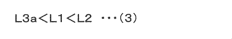

図5には、N型ソース領域9とN型ドレイン領域8の間に400Vの電圧を加え、P型基板1の電位をその中間電位の200Vとした場合の等電位線分布を示しているが、第2のフィールドプレートを複数の配線層51,55で構成することにより、単層で構成する場合に比べて、半導体基板1の表面に沿って均一な不純物濃度をもつN型ドリフト領域6の電界分布をより均一にすることができる。
Figure 5 shows the equipotential distribution when a voltage of 400 V is applied between the N-
以上説明したように、本実施例の半導体装置であるN型LDMOS電界効果トランジスタ50では、第2のフィールドプレートは、ドレイン領域(N型ドレイン領域8)までの距離が異なる複数の配線層51,55からなり、複数の配線層51,55において、上層にある配線層55のドレイン領域(N型ドレイン領域8)との距離(L3a)は、下層にある配線層51のドレイン領域(N型ドレイン領域8)との距離(L3b)よりも短く、最上層の配線層55のドレイン領域(N型ドレイン領域8)との距離(L3a)は、埋め込み領域(P型埋め込み領域4)のドレイン領域(N型ドレイン領域8)との距離(L1)よりも短く、最下層の配線層51のドレイン領域(N型ドレイン領域8)との距離(L3b)は、第1のフィールドプレート12のドレイン領域(N型ドレイン領域8)との距離(L2)よりも短くなるように構成されている。
As described above, in the N-type LDMOS
この結果、オフ状態時におけるN型ドリフト領域6の電界集中を抑えて、電界をより広い範囲で均一化することができるため、より高耐圧で、低オン抵抗な特性を得ることができる。
As a result, it is possible to suppress electric field concentration in the N-
図6を参照して、本発明の第4の実施形態の半導体装置について説明する。本実施例では、本発明をダイオードに適用した例を説明する。 With reference to FIG. 6, a semiconductor device according to a fourth embodiment of the present invention will be described. In this example, an example in which the present invention is applied to a diode will be described.
本実施例の半導体装置は、図6に示すように、ダイオード60であり、N型ドリフト領域6上にはN型カソード領域61が形成され、P型ボディ領域5上にはP型アノード領域62が形成されている。P型ボディ領域5及びN型ドリフト領域6の一部上部に、P型アノード領域62と接するように形成された酸化膜63上にポリSiで構成された第1のフィールドプレート64が形成されている。
As shown in FIG. 6, the semiconductor device of this embodiment is a
P型アノード領域62は、アノード領域引出しコンタクト66を介して、アノード電極及び第2のフィールドプレート69に接続されている。さらに、第1のフィールドプレート64と第2のフィールドプレート69は接続コンタクト68を介して接続されている。第1のフィールドプレート(及びゲート電極)64は、第2のフィールドプレート69を介してP型ボディ領域5と電気的に接続されている。
The P-
ここで、P型埋め込み領域4とN型カソード領域61との半導体基板1の表面に沿った距離をL1とし、また、第1のフィールドプレート64とN型カソード領域61との半導体基板1の表面に沿った距離をL2とし、また、第2のフィールドプレート69とN型カソード領域61との半導体表面に沿った距離をL3としたとき、L1、L2、L3は実施例1(図1)と同様に、上記の式(1)の関係にある。
Here, if the distance along the surface of the
これにより、第1のフィールドプレート64の端部近傍における電界集中を、P型埋め込み領域4によって抑制すると同時に、P型埋め込み領域4の端部近傍における電界集中を第2のフィールドプレート69によって抑制することができる。
As a result, the electric field concentration near the end of the
この結果、N型ドリフト領域6の不純物濃度が1e16/cm3以上となる高い場合においても、高耐圧を維持することができ、素子を小型化できる。
As a result, even when the impurity concentration in the N-
また、N型ドリフト領域6の不純物濃度を上げることで、リカバリー時間を短縮できるため、リカバリー損失の低減ができると共に、高注入効果による順方向電流の減少を抑制することができる。
In addition, by increasing the impurity concentration in the N-
以上説明したように、本発明の各実施例によれば、ドリフト領域の不純物濃度1e16/cm3以上で、ドリフト領域下のP型エピタキシャル層やP型基板(P型のSOI層3、バルクSi基板を用いる場合はP型半導体基板1)の不純物濃度に比べて1桁以上大きく、RESURF効果が小さくなる場合においても、P型埋め込み領域(或いはN型埋め込み領域)近傍における電界集中を抑えて、ドリフト領域における電界強度を均一とすることができるため、高耐圧を維持しながら、オン抵抗を低減することができる。
As described above, according to each embodiment of the present invention, even when the impurity concentration of the drift region is 1e16/ cm3 or more, which is greater by one order of magnitude than the impurity concentration of the P-type epitaxial layer or P-type substrate (P-
また、基板の電位がソース電位と異なり(同電位ではなく)、基板からのRESURF効果が小さくなる又は無くなる場合においても、P型埋め込み領域(或いはN型埋め込み領域)近傍における電界集中を抑えて、ドリフト領域の電界強度を均一とすることができる。このため、ドリフト領域の不純物濃度を低減することなく、言い換えるとオン抵抗を増大することなく、高耐圧を維持できる。 In addition, even if the substrate potential is different from the source potential (not the same potential) and the RESURF effect from the substrate is reduced or eliminated, the electric field concentration near the P-type buried region (or N-type buried region) can be suppressed and the electric field strength in the drift region can be made uniform. This makes it possible to maintain a high breakdown voltage without reducing the impurity concentration in the drift region, in other words, without increasing the on-resistance.
なお、本発明は上記した実施例に限定されるものではなく、様々な変形例が含まれる。例えば、上記した実施例は本発明を分かりやすく説明するために詳細に説明したものであり、必ずしも説明した全ての構成を備えるものに限定されるものではない。また、ある実施例の構成の一部を他の実施例の構成に置き換えることが可能であり、また、ある実施例の構成に他の実施例の構成を加えることも可能である。また、各実施例の構成の一部について、他の構成の追加・削除・置換をすることが可能である。 The present invention is not limited to the above-described embodiments, but includes various modified examples. For example, the above-described embodiments have been described in detail to clearly explain the present invention, and are not necessarily limited to those having all of the configurations described. It is also possible to replace part of the configuration of one embodiment with the configuration of another embodiment, and it is also possible to add the configuration of another embodiment to the configuration of one embodiment. It is also possible to add, delete, or replace part of the configuration of each embodiment with other configurations.
0,50,100…N型LDMOS電界効果トランジスタ
1,101…P型(半導体)基板
2…絶縁層
3…(P型の)SOI層
4…P型埋め込み領域
5,105…(P型)ボディ領域
6…N型ドリフト領域
7…絶縁層
8…N型ドレイン領域
9…N型ソース領域
10…P型(給電)領域
11…ゲート酸化膜
12…ゲート電極(第1のフィールドプレート)
13…絶縁層
14,15,53,54…コンタクト
16…配線層(ソース電極,第2のフィールドプレート)
17…配線層(ドレイン電極)
18…P型埋め込み領域4(第1のフィールドプレート12の端部)近傍の領域
19…P型埋め込み領域4の端部近傍の領域
30…P型LDMOS電界効果トランジスタ
34…N型埋め込み領域
35…(N型)ボディ領域
36…P型ドリフト領域
38…P型ドレイン領域
39…P型ソース領域
40…N型(給電)領域
51…第1の配線層(第2のフィールドプレート)
52,56…(第2の配線層の)ドレイン電極
55…第2の配線層(第2のフィールドプレート)
60…ダイオード
61…N型カソード領域
62…P型アノード領域
63…(シリコン)酸化膜
64…第1のフィールドプレート(ゲート電極,ポリシリコン)
65…絶縁層
66…(アノード領域引出し)コンタクト
67…(カソード領域引出し)コンタクト
68…(接続)コンタクト
69…アノード電極(第2のフィールドプレート)
70…カソード電極
102…P型エピタキシャル層
103…P+埋め込み領域
104…高濃度P+層
105…P型ボディ領域
106…ドリフト領域
107…ドレイン領域
108…ソース領域
109…ボディ領域給電領域
110…ゲート酸化膜
111…ゲート電極
112…絶縁層
113…ソース領域・ボディ領域引き出しコンタクト
114…ドレイン領域引出しコンタクト
115…ソース電極
116…ドレイン電極
117…ゲートフィールドプレート
118…絶縁層
119…SOI層
120…P+埋め込み領域103の端部近傍(電界が大きくなる領域)
0,50,100...N-type LDMOS field effect transistor 1,101...P-type (semiconductor) substrate 2...Insulating
13: Insulating
17...wiring layer (drain electrode)
18: Region in the vicinity of the P-type buried region 4 (end of the first field plate 12) 19: Region in the vicinity of the end of the P-type buried
52, 56...Drain electrode (of second wiring layer) 55...Second wiring layer (second field plate)
60: Diode 61: N-type cathode region 62: P-type anode region 63: (silicon) oxide film 64: First field plate (gate electrode, polysilicon)
65: Insulating layer 66: (anode region lead) contact 67: (cathode region lead) contact 68: (connection) contact 69: Anode electrode (second field plate)
70: Cathode electrode 102: P-type epitaxial layer 103: P+ buried region 104: High concentration P+ layer 105: P-type body region 106: Drift region 107: Drain region 108: Source region 109: Body region power supply region 110: Gate oxide film 111: Gate electrode 112: Insulating layer 113: Source region/body region draw-out contact 114: Drain region draw-out contact 115: Source electrode 116: Drain electrode 117: Gate field plate 118: Insulating layer 119: SOI layer 120: Near the end of the P+ buried region 103 (region where the electric field becomes large)
Claims (7)
前記半導体基板上に、埋め込み絶縁層を介して形成されたSOI層と、
前記SOI層に形成された第1導電型のボディ領域と、
前記ボディ領域の表面に形成された第2導電型のソース領域と、
前記ボディ領域と接するように、前記SOI層に形成された第2導電型のドリフト領域と、
前記ドリフト領域上に形成された第2導電型のドレイン領域と、
前記ボディ領域に接し、前記ドリフト領域の下方で前記ドリフト領域に接するように、前記SOI層に形成された第1導電型の埋め込み領域と、
前記ソース領域と前記ドリフト領域との間の前記ボディ領域及び前記ソース領域側の前記ドリフト領域上に、ゲート絶縁膜を介して形成されたゲート電極と、
前記ゲート電極から前記ドレイン領域方向に延在し、前記ドリフト領域上に第1の絶縁膜を介して形成された、第1のフィールドプレートと、
前記ソース領域に接し、前記第1のフィールドプレート上に第2の絶縁膜を介して形成された、第2のフィールドプレートと、を備え、
前記埋め込み領域と前記ドレイン領域との距離は、前記第1のフィールドプレートと前記ドレイン領域との距離よりも短く、
前記第2のフィールドプレートと前記ドレイン領域との距離よりも長く、
前記半導体基板の電圧は、前記ドレイン領域の電圧と前記ソース領域の電圧との中間の電位にあることを特徴とする半導体装置。 A semiconductor substrate ;
an SOI layer formed on the semiconductor substrate via a buried insulating layer;
a body region of a first conductivity type formed in the SOI layer ;
a source region of a second conductivity type formed on a surface of the body region;
a drift region of a second conductivity type formed in the SOI layer so as to be in contact with the body region;
a drain region of a second conductivity type formed on the drift region;
a buried region of a first conductivity type formed in the SOI layer in contact with the body region and below the drift region;
a gate electrode formed on the body region between the source region and the drift region and on the drift region on the source region side via a gate insulating film;
a first field plate extending from the gate electrode toward the drain region and formed on the drift region via a first insulating film;
a second field plate in contact with the source region and formed on the first field plate with a second insulating film interposed therebetween;
a distance between the buried region and the drain region is shorter than a distance between the first field plate and the drain region;
a distance between the second field plate and the drain region ;
4. A semiconductor device comprising: a semiconductor substrate having a potential at an intermediate potential between a potential of the drain region and a potential of the source region ;
前記第2のフィールドプレートは、前記ドレイン領域までの距離が異なる複数の配線層からなり、
前記複数の配線層において、上層にある配線層の前記ドレイン領域との距離は、下層にある配線層の前記ドレイン領域との距離よりも短く、
最上層の配線層の前記ドレイン領域との距離は、前記埋め込み領域の前記ドレイン領域との距離よりも短く、
最下層の配線層の前記ドレイン領域との距離は、前記第1のフィールドプレートの前記ドレイン領域との距離よりも短いことを特徴とする半導体装置。 2. The semiconductor device according to claim 1,
the second field plate is made up of a plurality of wiring layers having different distances to the drain region;
In the plurality of wiring layers, a distance between an upper wiring layer and the drain region is shorter than a distance between a lower wiring layer and the drain region;
a distance between the uppermost wiring layer and the drain region is shorter than a distance between the buried region and the drain region;
1. A semiconductor device comprising: a first field plate and a second field plate arranged in a first direction such that the first field plate and the second field plate are spaced apart from each other by a distance between the first field plate and the drain region;
前記ドリフト領域の最大不純物濃度は1e16/cm3以上であり、
前記埋め込み領域の最大不純物濃度は、前記埋め込み領域上の前記ドリフト領域の最大不純物濃度に対し1/3倍以上、1倍以下であることを特徴とする半導体装置。 2. The semiconductor device according to claim 1,
The maximum impurity concentration of the drift region is 1e16/cm3 or more,
A semiconductor device, characterized in that a maximum impurity concentration of the buried region is 1/3 to 1 time the maximum impurity concentration of the drift region above the buried region.
前記ボディ領域及び前記ドレイン領域間において、前記ドリフト領域が前記半導体基板の主面に沿って延在するLDMOSであることを特徴とする半導体装置。 2. The semiconductor device according to claim 1,
1. A semiconductor device comprising: an LDMOS in which the drift region extends along a main surface of the semiconductor substrate between the body region and the drain region.
前記半導体基板上に、埋め込み絶縁層を介して形成されたSOI層と、
前記SOI層に形成された第1導電型のボディ領域と、
前記ボディ領域の表面に形成された第2導電型のソース領域と、
前記ボディ領域と接するように、前記SOI層に形成された第2導電型のドリフト領域と、
前記ドリフト領域上に形成された第2導電型のドレイン領域と、
前記ボディ領域に接し、前記ドリフト領域の下方で前記ドリフト領域に接するように、前記SOI層に形成された第1導電型の埋め込み領域と、
前記ソース領域と前記ドリフト領域との間の前記ボディ領域及び前記ソース領域側の前記ドリフト領域上に、ゲート絶縁膜を介して形成されたゲート電極と、
前記ゲート電極から前記ドレイン領域方向に延在し、前記ドリフト領域上に第1の絶縁膜を介して形成された、第1のフィールドプレートと、
前記ソース領域に接し、前記第1のフィールドプレート上に第2の絶縁膜を介して形成された、第2のフィールドプレートと、を備え、
前記埋め込み領域と前記ドレイン領域との距離は、前記第1のフィールドプレートと前記ドレイン領域との距離よりも短く、
前記第2のフィールドプレートと前記ドレイン領域との距離よりも長く、
前記半導体基板の電圧は、前記ドレイン領域の電圧と等しいことを特徴とする半導体装置。 A semiconductor substrate;
an SOI layer formed on the semiconductor substrate via a buried insulating layer;
a body region of a first conductivity type formed in the SOI layer;
a source region of a second conductivity type formed on a surface of the body region;
a drift region of a second conductivity type formed in the SOI layer so as to be in contact with the body region;
a drain region of a second conductivity type formed on the drift region;
a buried region of a first conductivity type formed in the SOI layer in contact with the body region and below the drift region;
a gate electrode formed on the body region between the source region and the drift region and on the drift region on the source region side via a gate insulating film;
a first field plate extending from the gate electrode toward the drain region and formed on the drift region via a first insulating film;
a second field plate in contact with the source region and formed on the first field plate with a second insulating film interposed therebetween;
a distance between the buried region and the drain region is shorter than a distance between the first field plate and the drain region;
longer than the distance between the second field plate and the drain region,
A semiconductor device, characterized in that the voltage of the semiconductor substrate is equal to the voltage of the drain region.
前記半導体基板上に、埋め込み絶縁層を介して形成されたSOI層と、an SOI layer formed on the semiconductor substrate via a buried insulating layer;
前記SOI層に形成された第1導電型のボディ領域と、a body region of a first conductivity type formed in the SOI layer;
前記ボディ領域の表面に形成された第2導電型のソース領域と、a source region of a second conductivity type formed on a surface of the body region;
前記ボディ領域と接するように、前記SOI層に形成された第2導電型のドリフト領域と、a drift region of a second conductivity type formed in the SOI layer so as to be in contact with the body region;
前記ドリフト領域上に形成された第2導電型のドレイン領域と、a drain region of a second conductivity type formed on the drift region;
前記ボディ領域に接し、前記ドリフト領域の下方で前記ドリフト領域に接するように、前記SOI層に形成された第1導電型の埋め込み領域と、a buried region of a first conductivity type formed in the SOI layer in contact with the body region and below the drift region;
前記ソース領域と前記ドリフト領域との間の前記ボディ領域及び前記ソース領域側の前記ドリフト領域上に、ゲート絶縁膜を介して形成されたゲート電極と、a gate electrode formed on the body region between the source region and the drift region and on the drift region on the source region side via a gate insulating film;
前記ゲート電極から前記ドレイン領域方向に延在し、前記ドリフト領域上に第1の絶縁膜を介して形成された、第1のフィールドプレートと、a first field plate extending from the gate electrode toward the drain region and formed on the drift region via a first insulating film;
前記ソース領域に接し、前記第1のフィールドプレート上に第2の絶縁膜を介して形成された、第2のフィールドプレートと、を備え、a second field plate in contact with the source region and formed on the first field plate with a second insulating film interposed therebetween;
前記埋め込み領域と前記ドレイン領域との距離は、前記第1のフィールドプレートと前記ドレイン領域との距離よりも短く、a distance between the buried region and the drain region is shorter than a distance between the first field plate and the drain region;
前記第2のフィールドプレートと前記ドレイン領域との距離よりも長く、longer than the distance between the second field plate and the drain region,
前記半導体基板の電圧は、前記ソース領域の電圧と等しいか、又は0Vであることを特徴とする半導体装置。A semiconductor device, characterized in that the voltage of the semiconductor substrate is equal to the voltage of the source region or is 0V.
前記半導体基板上に、埋め込み絶縁層を介して形成されたSOI層と、
前記SOI層に形成された第1導電型のボディ領域と、
前記ボディ領域の表面に形成された第2導電型のエミッタ領域と、
前記ボディ領域と接するように、前記SOI層に形成された第2導電型のドリフト領域と、
前記ドリフト領域上に形成された第1導電型のコレクタ領域と、
前記ボディ領域に接し、前記ドリフト領域の下方で前記ドリフト領域に接するように、前記SOI層に形成された第1導電型の埋め込み領域と、
前記エミッタ領域と前記ドリフト領域との間の前記ボディ領域及び前記エミッタ領域側の前記ドリフト領域上に、ゲート絶縁膜を介して形成されたゲート電極と、
前記ゲート電極から前記コレクタ領域方向に延在し、前記ドリフト領域上に第1の絶縁膜を介して形成された、第1のフィールドプレートと、
前記エミッタ領域に接し、前記第1のフィールドプレート上に第2の絶縁膜を介して形成された、第2のフィールドプレートと、を備え、
前記埋め込み領域と前記コレクタ領域との距離は、前記第1のフィールドプレートと前記コレクタ領域との距離よりも短く、
前記第2のフィールドプレートと前記コレクタ領域との距離よりも長く、
前記半導体基板の電圧は、前記コレクタ領域の電圧と前記エミッタ領域の電圧との中間の電位にあることを特徴とする半導体装置。
A semiconductor substrate ;
an SOI layer formed on the semiconductor substrate via a buried insulating layer;
a body region of a first conductivity type formed in the SOI layer ;
an emitter region of a second conductivity type formed on a surface of the body region;
a drift region of a second conductivity type formed in the SOI layer so as to be in contact with the body region;
a collector region of a first conductivity type formed on the drift region;
a buried region of a first conductivity type formed in the SOI layer in contact with the body region and below the drift region;
a gate electrode formed on the body region between the emitter region and the drift region and on the drift region on the emitter region side via a gate insulating film;
a first field plate extending from the gate electrode toward the collector region and formed on the drift region via a first insulating film;
a second field plate in contact with the emitter region and formed on the first field plate with a second insulating film interposed therebetween;
a distance between the buried region and the collector region is shorter than a distance between the first field plate and the collector region;
a distance between the second field plate and the collector region ;
4. A semiconductor device comprising: a first region and a second region, the first region being electrically connected to the first collector region; a second region being electrically connected to the first emitter region ;
Priority Applications (7)
| Application Number | Priority Date | Filing Date | Title |
|---|---|---|---|
| JP2018237115A JP7569144B2 (en) | 2018-12-19 | 2018-12-19 | Semiconductor Device |
| EP19897840.5A EP3901993A4 (en) | 2018-12-19 | 2019-10-11 | SEMICONDUCTOR DEVICE |
| PCT/JP2019/040216 WO2020129375A1 (en) | 2018-12-19 | 2019-10-11 | Semiconductor device |
| US17/312,663 US12230710B2 (en) | 2018-12-19 | 2019-10-11 | LDMOS with field plates |
| JP2023000358A JP7442699B2 (en) | 2018-12-19 | 2023-01-05 | semiconductor equipment |
| JP2023119428A JP7561928B2 (en) | 2018-12-19 | 2023-07-21 | Semiconductor Device |
| US19/015,236 US20250151316A1 (en) | 2018-12-19 | 2025-01-09 | Semiconductor device |
Applications Claiming Priority (1)
| Application Number | Priority Date | Filing Date | Title |
|---|---|---|---|
| JP2018237115A JP7569144B2 (en) | 2018-12-19 | 2018-12-19 | Semiconductor Device |
Related Child Applications (2)
| Application Number | Title | Priority Date | Filing Date |
|---|---|---|---|
| JP2023000358A Division JP7442699B2 (en) | 2018-12-19 | 2023-01-05 | semiconductor equipment |
| JP2023119428A Division JP7561928B2 (en) | 2018-12-19 | 2023-07-21 | Semiconductor Device |
Publications (2)
| Publication Number | Publication Date |
|---|---|
| JP2020098883A JP2020098883A (en) | 2020-06-25 |
| JP7569144B2 true JP7569144B2 (en) | 2024-10-17 |
Family
ID=71102769
Family Applications (3)
| Application Number | Title | Priority Date | Filing Date |
|---|---|---|---|
| JP2018237115A Active JP7569144B2 (en) | 2018-12-19 | 2018-12-19 | Semiconductor Device |
| JP2023000358A Active JP7442699B2 (en) | 2018-12-19 | 2023-01-05 | semiconductor equipment |
| JP2023119428A Active JP7561928B2 (en) | 2018-12-19 | 2023-07-21 | Semiconductor Device |
Family Applications After (2)
| Application Number | Title | Priority Date | Filing Date |
|---|---|---|---|
| JP2023000358A Active JP7442699B2 (en) | 2018-12-19 | 2023-01-05 | semiconductor equipment |
| JP2023119428A Active JP7561928B2 (en) | 2018-12-19 | 2023-07-21 | Semiconductor Device |
Country Status (4)
| Country | Link |
|---|---|
| US (2) | US12230710B2 (en) |
| EP (1) | EP3901993A4 (en) |
| JP (3) | JP7569144B2 (en) |
| WO (1) | WO2020129375A1 (en) |
Families Citing this family (12)
| Publication number | Priority date | Publication date | Assignee | Title |
|---|---|---|---|---|
| CN111092123A (en) * | 2019-12-10 | 2020-05-01 | 杰华特微电子(杭州)有限公司 | Lateral double diffused transistor and method of making the same |
| US11476244B2 (en) | 2020-08-19 | 2022-10-18 | Globalfoundries Singapore Pte. Ltd. | Laterally-diffused metal-oxide-semiconductor devices for electrostatic discharge protection applications |
| EP4258363A4 (en) * | 2020-12-01 | 2024-02-14 | Nissan Motor Co., Ltd. | SEMICONDUCTOR COMPONENT AND PRODUCTION METHOD THEREOF |
| US11673796B2 (en) * | 2021-03-09 | 2023-06-13 | Palo Alto Research Center Incorporated | Scalable high-voltage control circuits using thin film electronics |
| US12002888B2 (en) * | 2021-03-09 | 2024-06-04 | Xerox Corporation | Switching device for driving an actuator |
| TWI762253B (en) * | 2021-03-25 | 2022-04-21 | 力晶積成電子製造股份有限公司 | Semiconductor device |
| JP7662470B2 (en) * | 2021-09-17 | 2025-04-15 | シャープ福山レーザー株式会社 | Semiconductor Device |
| JP7731265B2 (en) * | 2021-11-18 | 2025-08-29 | エイブリック株式会社 | Semiconductor Devices |
| JP2023137588A (en) * | 2022-03-18 | 2023-09-29 | 株式会社デンソー | Semiconductor device |
| CN114864666B (en) * | 2022-07-11 | 2023-02-24 | 北京芯可鉴科技有限公司 | NLDMOS device, preparation method and chip of NLDMOS device |
| CN116053292A (en) * | 2022-08-05 | 2023-05-02 | 北京智慧能源研究院 | An Insulated Gate Bipolar Transistor |
| CN118800805B (en) * | 2024-09-11 | 2024-12-17 | 粤芯半导体技术股份有限公司 | Semiconductor device and method for manufacturing the same |
Citations (3)
| Publication number | Priority date | Publication date | Assignee | Title |
|---|---|---|---|---|
| JP2002270830A (en) | 2001-03-12 | 2002-09-20 | Fuji Electric Co Ltd | Semiconductor device |
| US20140284701A1 (en) | 2012-07-31 | 2014-09-25 | Azure Silicon LLC | Power device integration on a common substrate |
| US20170222042A1 (en) | 2016-01-28 | 2017-08-03 | Texas Instruments Incorporated | Soi power ldmos device |
Family Cites Families (7)
| Publication number | Priority date | Publication date | Assignee | Title |
|---|---|---|---|---|
| US5374843A (en) | 1991-05-06 | 1994-12-20 | Silinconix, Inc. | Lightly-doped drain MOSFET with improved breakdown characteristics |
| BE1007283A3 (en) * | 1993-07-12 | 1995-05-09 | Philips Electronics Nv | Semiconductor device with most with an extended drain area high voltage. |
| US9159828B2 (en) * | 2011-04-27 | 2015-10-13 | Alpha And Omega Semiconductor Incorporated | Top drain LDMOS |
| JP6030923B2 (en) * | 2012-11-09 | 2016-11-24 | シャープ株式会社 | Semiconductor device and manufacturing method thereof |
| JP6244177B2 (en) * | 2013-11-12 | 2017-12-06 | 日立オートモティブシステムズ株式会社 | Semiconductor device |
| JP6229646B2 (en) | 2013-12-20 | 2017-11-15 | 株式会社デンソー | Semiconductor device |
| US9722063B1 (en) * | 2016-04-11 | 2017-08-01 | Power Integrations, Inc. | Protective insulator for HFET devices |
-
2018
- 2018-12-19 JP JP2018237115A patent/JP7569144B2/en active Active
-
2019
- 2019-10-11 US US17/312,663 patent/US12230710B2/en active Active
- 2019-10-11 WO PCT/JP2019/040216 patent/WO2020129375A1/en not_active Ceased
- 2019-10-11 EP EP19897840.5A patent/EP3901993A4/en active Pending
-
2023
- 2023-01-05 JP JP2023000358A patent/JP7442699B2/en active Active
- 2023-07-21 JP JP2023119428A patent/JP7561928B2/en active Active
-
2025
- 2025-01-09 US US19/015,236 patent/US20250151316A1/en active Pending
Patent Citations (3)
| Publication number | Priority date | Publication date | Assignee | Title |
|---|---|---|---|---|
| JP2002270830A (en) | 2001-03-12 | 2002-09-20 | Fuji Electric Co Ltd | Semiconductor device |
| US20140284701A1 (en) | 2012-07-31 | 2014-09-25 | Azure Silicon LLC | Power device integration on a common substrate |
| US20170222042A1 (en) | 2016-01-28 | 2017-08-03 | Texas Instruments Incorporated | Soi power ldmos device |
Also Published As
| Publication number | Publication date |
|---|---|
| JP2020098883A (en) | 2020-06-25 |
| EP3901993A4 (en) | 2022-09-14 |
| JP7442699B2 (en) | 2024-03-04 |
| JP2023026604A (en) | 2023-02-24 |
| US20250151316A1 (en) | 2025-05-08 |
| WO2020129375A1 (en) | 2020-06-25 |
| JP7561928B2 (en) | 2024-10-04 |
| EP3901993A1 (en) | 2021-10-27 |
| JP2023126662A (en) | 2023-09-07 |
| US20220052197A1 (en) | 2022-02-17 |
| US12230710B2 (en) | 2025-02-18 |
Similar Documents
| Publication | Publication Date | Title |
|---|---|---|
| JP7561928B2 (en) | Semiconductor Device | |
| US7898024B2 (en) | Semiconductor device and method for manufacturing the same | |
| US8546875B1 (en) | Vertical transistor having edge termination structure | |
| CN103035641B (en) | Semiconductor device | |
| CN107452800A (en) | LDMOS transistors and related systems and methods | |
| WO2012055225A1 (en) | High voltage ldmos device | |
| CN104299995A (en) | Semiconductor device | |
| JP6907233B2 (en) | Power semiconductor device | |
| CN104106133A (en) | Semiconductor arrangement with active drift zone | |
| CN103137661B (en) | Lateral double-diffused metal-oxide semiconductor device and its manufacture method | |
| JP2019161188A (en) | Semiconductor device | |
| CN106992212B (en) | Transistor device with increased gate-drain capacitance | |
| CN103915506A (en) | Double-gate LDMOS device with longitudinal NPN structure | |
| JP2011517511A (en) | A semiconductor device in which a first insulated gate field effect transistor is connected in series with a second field effect transistor | |
| US20250113567A1 (en) | Lateral high voltage semiconductor device and method for forming a lateral high voltage semiconductor device | |
| WO2015145913A1 (en) | Semiconductor device | |
| CN105917469A (en) | Power semiconductor device | |
| JP7731265B2 (en) | Semiconductor Devices | |
| CN113871452B (en) | Semiconductor device with a semiconductor layer having a plurality of semiconductor layers | |
| JP7326991B2 (en) | switching element | |
| JP2008288510A (en) | Semiconductor device | |
| JP2018056380A (en) | Switching element | |
| CN107026203A (en) | Semiconductor devices and its manufacture method | |
| US9502498B2 (en) | Power semiconductor device | |
| JP2021086890A (en) | Semiconductor device |
Legal Events
| Date | Code | Title | Description |
|---|---|---|---|
| A711 | Notification of change in applicant |
Free format text: JAPANESE INTERMEDIATE CODE: A711 Effective date: 20210614 |
|
| A521 | Request for written amendment filed |
Free format text: JAPANESE INTERMEDIATE CODE: A821 Effective date: 20210614 |
|
| A621 | Written request for application examination |
Free format text: JAPANESE INTERMEDIATE CODE: A621 Effective date: 20211111 |
|
| A131 | Notification of reasons for refusal |
Free format text: JAPANESE INTERMEDIATE CODE: A131 Effective date: 20221108 |
|
| A521 | Request for written amendment filed |
Free format text: JAPANESE INTERMEDIATE CODE: A523 Effective date: 20221227 |
|
| A02 | Decision of refusal |
Free format text: JAPANESE INTERMEDIATE CODE: A02 Effective date: 20230425 |
|
| A521 | Request for written amendment filed |
Free format text: JAPANESE INTERMEDIATE CODE: A523 Effective date: 20230721 |
|
| A911 | Transfer to examiner for re-examination before appeal (zenchi) |
Free format text: JAPANESE INTERMEDIATE CODE: A911 Effective date: 20230731 |
|
| A912 | Re-examination (zenchi) completed and case transferred to appeal board |
Free format text: JAPANESE INTERMEDIATE CODE: A912 Effective date: 20230929 |
|
| A521 | Request for written amendment filed |
Free format text: JAPANESE INTERMEDIATE CODE: A523 Effective date: 20240625 |
|
| A521 | Request for written amendment filed |
Free format text: JAPANESE INTERMEDIATE CODE: A523 Effective date: 20240806 |
|
| A61 | First payment of annual fees (during grant procedure) |
Free format text: JAPANESE INTERMEDIATE CODE: A61 Effective date: 20241004 |
|
| R150 | Certificate of patent or registration of utility model |
Ref document number: 7569144 Country of ref document: JP Free format text: JAPANESE INTERMEDIATE CODE: R150 |