JP7534146B2 - Magnetic sensor system and lens position detection device - Google Patents
Magnetic sensor system and lens position detection device Download PDFInfo
- Publication number
- JP7534146B2 JP7534146B2 JP2020132658A JP2020132658A JP7534146B2 JP 7534146 B2 JP7534146 B2 JP 7534146B2 JP 2020132658 A JP2020132658 A JP 2020132658A JP 2020132658 A JP2020132658 A JP 2020132658A JP 7534146 B2 JP7534146 B2 JP 7534146B2
- Authority
- JP
- Japan
- Prior art keywords
- magnetic field
- magnetic
- magnetic sensor
- strength
- sensor system
- Prior art date
- Legal status (The legal status is an assumption and is not a legal conclusion. Google has not performed a legal analysis and makes no representation as to the accuracy of the status listed.)
- Active
Links
- 238000001514 detection method Methods 0.000 title claims description 204
- 230000005415 magnetization Effects 0.000 claims description 38
- 230000000694 effects Effects 0.000 claims description 29
- 230000004888 barrier function Effects 0.000 claims description 3
- 230000004907 flux Effects 0.000 description 70
- 239000003795 chemical substances by application Substances 0.000 description 26
- 238000004088 simulation Methods 0.000 description 26
- 238000010586 diagram Methods 0.000 description 24
- 230000008859 change Effects 0.000 description 14
- 230000007423 decrease Effects 0.000 description 12
- 230000005484 gravity Effects 0.000 description 7
- 238000004364 calculation method Methods 0.000 description 5
- 239000000758 substrate Substances 0.000 description 4
- 238000000034 method Methods 0.000 description 3
- 230000004044 response Effects 0.000 description 3
- 230000003247 decreasing effect Effects 0.000 description 2
- 230000004048 modification Effects 0.000 description 2
- 238000012986 modification Methods 0.000 description 2
- 230000009471 action Effects 0.000 description 1
- 238000009434 installation Methods 0.000 description 1
- 238000004519 manufacturing process Methods 0.000 description 1
- 230000003287 optical effect Effects 0.000 description 1
- 230000001151 other effect Effects 0.000 description 1
- 229920006395 saturated elastomer Polymers 0.000 description 1
- 230000035945 sensitivity Effects 0.000 description 1
- 230000035939 shock Effects 0.000 description 1
Images


Classifications
-
- G—PHYSICS
- G01—MEASURING; TESTING
- G01V—GEOPHYSICS; GRAVITATIONAL MEASUREMENTS; DETECTING MASSES OR OBJECTS; TAGS
- G01V3/00—Electric or magnetic prospecting or detecting; Measuring magnetic field characteristics of the earth, e.g. declination, deviation
- G01V3/08—Electric or magnetic prospecting or detecting; Measuring magnetic field characteristics of the earth, e.g. declination, deviation operating with magnetic or electric fields produced or modified by objects or geological structures or by detecting devices
- G01V3/081—Electric or magnetic prospecting or detecting; Measuring magnetic field characteristics of the earth, e.g. declination, deviation operating with magnetic or electric fields produced or modified by objects or geological structures or by detecting devices the magnetic field is produced by the objects or geological structures
-
- G—PHYSICS
- G01—MEASURING; TESTING
- G01R—MEASURING ELECTRIC VARIABLES; MEASURING MAGNETIC VARIABLES
- G01R33/00—Arrangements or instruments for measuring magnetic variables
- G01R33/02—Measuring direction or magnitude of magnetic fields or magnetic flux
- G01R33/06—Measuring direction or magnitude of magnetic fields or magnetic flux using galvano-magnetic devices
- G01R33/09—Magnetoresistive devices
- G01R33/091—Constructional adaptation of the sensor to specific applications
-
- G—PHYSICS
- G01—MEASURING; TESTING
- G01D—MEASURING NOT SPECIALLY ADAPTED FOR A SPECIFIC VARIABLE; ARRANGEMENTS FOR MEASURING TWO OR MORE VARIABLES NOT COVERED IN A SINGLE OTHER SUBCLASS; TARIFF METERING APPARATUS; MEASURING OR TESTING NOT OTHERWISE PROVIDED FOR
- G01D5/00—Mechanical means for transferring the output of a sensing member; Means for converting the output of a sensing member to another variable where the form or nature of the sensing member does not constrain the means for converting; Transducers not specially adapted for a specific variable
- G01D5/12—Mechanical means for transferring the output of a sensing member; Means for converting the output of a sensing member to another variable where the form or nature of the sensing member does not constrain the means for converting; Transducers not specially adapted for a specific variable using electric or magnetic means
- G01D5/14—Mechanical means for transferring the output of a sensing member; Means for converting the output of a sensing member to another variable where the form or nature of the sensing member does not constrain the means for converting; Transducers not specially adapted for a specific variable using electric or magnetic means influencing the magnitude of a current or voltage
- G01D5/16—Mechanical means for transferring the output of a sensing member; Means for converting the output of a sensing member to another variable where the form or nature of the sensing member does not constrain the means for converting; Transducers not specially adapted for a specific variable using electric or magnetic means influencing the magnitude of a current or voltage by varying resistance
-
- G—PHYSICS
- G01—MEASURING; TESTING
- G01D—MEASURING NOT SPECIALLY ADAPTED FOR A SPECIFIC VARIABLE; ARRANGEMENTS FOR MEASURING TWO OR MORE VARIABLES NOT COVERED IN A SINGLE OTHER SUBCLASS; TARIFF METERING APPARATUS; MEASURING OR TESTING NOT OTHERWISE PROVIDED FOR
- G01D5/00—Mechanical means for transferring the output of a sensing member; Means for converting the output of a sensing member to another variable where the form or nature of the sensing member does not constrain the means for converting; Transducers not specially adapted for a specific variable
- G01D5/12—Mechanical means for transferring the output of a sensing member; Means for converting the output of a sensing member to another variable where the form or nature of the sensing member does not constrain the means for converting; Transducers not specially adapted for a specific variable using electric or magnetic means
- G01D5/244—Mechanical means for transferring the output of a sensing member; Means for converting the output of a sensing member to another variable where the form or nature of the sensing member does not constrain the means for converting; Transducers not specially adapted for a specific variable using electric or magnetic means influencing characteristics of pulses or pulse trains; generating pulses or pulse trains
- G01D5/245—Mechanical means for transferring the output of a sensing member; Means for converting the output of a sensing member to another variable where the form or nature of the sensing member does not constrain the means for converting; Transducers not specially adapted for a specific variable using electric or magnetic means influencing characteristics of pulses or pulse trains; generating pulses or pulse trains using a variable number of pulses in a train
- G01D5/2451—Incremental encoders
-
- G—PHYSICS
- G01—MEASURING; TESTING
- G01R—MEASURING ELECTRIC VARIABLES; MEASURING MAGNETIC VARIABLES
- G01R33/00—Arrangements or instruments for measuring magnetic variables
- G01R33/02—Measuring direction or magnitude of magnetic fields or magnetic flux
- G01R33/06—Measuring direction or magnitude of magnetic fields or magnetic flux using galvano-magnetic devices
- G01R33/09—Magnetoresistive devices
- G01R33/093—Magnetoresistive devices using multilayer structures, e.g. giant magnetoresistance sensors
-
- G—PHYSICS
- G01—MEASURING; TESTING
- G01R—MEASURING ELECTRIC VARIABLES; MEASURING MAGNETIC VARIABLES
- G01R33/00—Arrangements or instruments for measuring magnetic variables
- G01R33/02—Measuring direction or magnitude of magnetic fields or magnetic flux
- G01R33/06—Measuring direction or magnitude of magnetic fields or magnetic flux using galvano-magnetic devices
- G01R33/09—Magnetoresistive devices
- G01R33/098—Magnetoresistive devices comprising tunnel junctions, e.g. tunnel magnetoresistance sensors
-
- G—PHYSICS
- G01—MEASURING; TESTING
- G01R—MEASURING ELECTRIC VARIABLES; MEASURING MAGNETIC VARIABLES
- G01R33/00—Arrangements or instruments for measuring magnetic variables
- G01R33/12—Measuring magnetic properties of articles or specimens of solids or fluids
- G01R33/123—Measuring loss due to hysteresis
Landscapes
- Physics & Mathematics (AREA)
- General Physics & Mathematics (AREA)
- Engineering & Computer Science (AREA)
- Remote Sensing (AREA)
- Life Sciences & Earth Sciences (AREA)
- Environmental & Geological Engineering (AREA)
- Geology (AREA)
- General Life Sciences & Earth Sciences (AREA)
- Electromagnetism (AREA)
- Geophysics (AREA)
- Condensed Matter Physics & Semiconductors (AREA)
- Measuring Magnetic Variables (AREA)
- Transmission And Conversion Of Sensor Element Output (AREA)
- Measurement Of Length, Angles, Or The Like Using Electric Or Magnetic Means (AREA)
- Hall/Mr Elements (AREA)
- Lens Barrels (AREA)
Description
本発明は、磁気センサシステムと、この磁気センサシステムを用いたレンズ位置検出装置に関する。 The present invention relates to a magnetic sensor system and a lens position detection device that uses this magnetic sensor system.
磁気センサを用いた磁気センサシステムとして、所定の範囲内で、磁気センサに対する磁気スケール等の磁界発生器の相対位置が変化するように構成された磁気センサシステムが知られている。磁気センサに対する磁界発生器の相対位置が変化すると、磁界発生器によって発生されて磁気センサに印加される対象磁界の一方向の成分の強度が変化する。磁気センサは、例えば、対象磁界の一方向の成分の強度を検出して、この一方向の成分の強度に対応し且つ互いに位相の異なる2つの検出信号を生成する。磁気センサシステムは、2つの検出信号に基づいて、磁気センサに対する磁界発生器の相対位置と対応関係を有する検出値を生成する。 A known magnetic sensor system using a magnetic sensor is one that is configured so that the relative position of a magnetic field generator, such as a magnetic scale, with respect to the magnetic sensor changes within a predetermined range. When the relative position of the magnetic field generator with respect to the magnetic sensor changes, the strength of the one-directional component of the target magnetic field generated by the magnetic field generator and applied to the magnetic sensor changes. The magnetic sensor, for example, detects the strength of the one-directional component of the target magnetic field and generates two detection signals that correspond to the strength of this one-directional component and are out of phase with each other. Based on the two detection signals, the magnetic sensor system generates a detection value that corresponds to the relative position of the magnetic field generator with respect to the magnetic sensor.
磁気センサシステムは、検出値を生成する検出値生成回路を備えている。一般的に、検出値生成回路の要部は、デジタルシグナルプロセッサ(DSP)、特定用途向け集積回路(ASIC)またはマイクロコンピュータによって構成されている。検出値生成回路は、アナログ-デジタル変換器(以下、A/D変換器とも記す。)によってデジタル信号に変換された磁気センサの検出信号に基づいて、検出値を生成する。 The magnetic sensor system includes a detection value generating circuit that generates a detection value. In general, the main components of the detection value generating circuit are configured with a digital signal processor (DSP), an application specific integrated circuit (ASIC), or a microcomputer. The detection value generating circuit generates a detection value based on the detection signal of the magnetic sensor that has been converted into a digital signal by an analog-to-digital converter (hereinafter also referred to as an A/D converter).
磁気センサシステムは、例えば、所定の方向に位置が変化する可動物体の位置を検出する位置検出装置に用いられる。以下、磁気センサシステムを用いた位置検出装置を、磁気式の位置検出装置と言う。磁気式の位置検出装置では、可動物体の位置の変化に対応して、磁気センサに対する磁界発生器の相対位置が変化するように構成されている。所定の方向は、直線的な方向または回転方向である。 The magnetic sensor system is used, for example, in a position detection device that detects the position of a movable object whose position changes in a predetermined direction. Hereinafter, a position detection device that uses a magnetic sensor system is referred to as a magnetic position detection device. In a magnetic position detection device, the relative position of a magnetic field generator with respect to the magnetic sensor is configured to change in response to a change in the position of the movable object. The predetermined direction is a linear direction or a rotational direction.
磁気式の位置検出装置は、例えば特許文献1ないし3に記載されている。特許文献1ないし3に記載された位置検出装置では、磁気検出素子として磁気抵抗効果素子(以下、MR素子とも記す。)が用いられている。MR素子は、磁気記録媒体または磁気スケールに対して所定の間隔を開けて配置されている。
Magnetic position detection devices are described, for example, in
ところで、磁気センサシステムおよび磁気式の位置検出装置では、高調波に起因して、磁気センサの検出信号の波形が歪むことが知られている。磁気センサの検出信号の出力波形が歪むと、磁気センサに対する磁界発生器の相対位置を精度よく検出することができなくなってしまう。これに対し、特許文献1に記載された位置検出装置では、MR素子に対してバイアス磁界を印加するバイアスマグネットを設けることによって、検出信号の高調波による歪み成分を除去している。
However, it is known that in magnetic sensor systems and magnetic position detection devices, the waveform of the detection signal of the magnetic sensor is distorted due to harmonics. If the output waveform of the detection signal of the magnetic sensor is distorted, it becomes impossible to accurately detect the relative position of the magnetic field generator with respect to the magnetic sensor. In response to this, the position detection device described in
また、特許文献3に記載された位置検出装置では、複数のMR素子(TMR素子)を、磁気スケールの長手方向に沿って、磁気スケールの記録信号の波長λまたはλの1/2のピッチPに基づいて配置することによって、検出信号の奇数次の高調波歪みをキャンセルしている。
In addition, in the position detection device described in
また、特許文献4には、磁気センサと棒形状の磁石とを備えた磁気エンコーダが記載されている。この磁気エンコーダでは、MR素子の近傍に軟磁性層を設け、これによりMR素子に印加される外部磁界を増幅して、MR素子の磁気検出感度を向上させている。
特許文献1ないし3に記載された位置検出装置および特許文献4に記載された磁気エンコーダのように、磁気センサが磁界発生器に対して所定の間隔を開けて配置された磁気センサシステムでは、磁気センサの設置の精度によって、磁気センサと磁界発生器との間隔がずれる場合がある。この間隔がずれると、検出値生成回路に入力される磁気センサの検出信号の大きさがずれてしまう。そのため、従来は、ロット毎または製品毎に検出信号の較正が必要であり、手間がかかるという問題があった。
In magnetic sensor systems in which a magnetic sensor is disposed at a predetermined distance from a magnetic field generator, such as the position detection devices described in
また、磁気センサと磁界発生器との間隔が小さくなるに従って、磁気センサに印加される対象磁界の強度が大きくなる。その結果、検出値生成回路に入力される磁気センサの検出信号の最大値が大きくなる。これにより、検出信号の大きさがA/D変換器の入力範囲を超えてしまい、検出値生成回路に入力される検出信号が飽和してしまう場合がある。検出信号が飽和すると、磁気センサシステムの検出精度が悪化するという問題が発生する。 In addition, as the distance between the magnetic sensor and the magnetic field generator decreases, the strength of the target magnetic field applied to the magnetic sensor increases. As a result, the maximum value of the detection signal of the magnetic sensor input to the detection value generation circuit increases. This can cause the magnitude of the detection signal to exceed the input range of the A/D converter, resulting in saturation of the detection signal input to the detection value generation circuit. When the detection signal becomes saturated, the detection accuracy of the magnetic sensor system deteriorates.
一般的に、検出信号は、増幅器によって所定のゲインを乗じた上で、A/D変換器に入力される。検出信号の飽和を防止するために、磁気センサと磁界発生器との最小の間隔を想定して、ゲインを設定することが考えられる。しかし、そうすると、A/D変換器の入力範囲の全体を用いることができなくなり、分解能が低下して検出精度が悪化するという問題が発生する。 Generally, the detection signal is multiplied by a predetermined gain by an amplifier before being input to the A/D converter. In order to prevent saturation of the detection signal, it is possible to set the gain assuming the minimum distance between the magnetic sensor and the magnetic field generator. However, doing so results in the problem that the entire input range of the A/D converter cannot be used, lowering the resolution and worsening the detection accuracy.
また、磁気センサと磁界発生器との間隔は、使用時の物理的な衝撃によってずれる場合もある。これによっても、検出信号が飽和して、磁気センサシステムの検出精度が悪化するという問題が発生する。 In addition, the distance between the magnetic sensor and the magnetic field generator may shift due to physical shock during use. This can also cause the detection signal to saturate, resulting in a problem of reduced detection accuracy of the magnetic sensor system.
本発明はかかる問題点に鑑みてなされたもので、その目的は、磁気センサと磁界発生器との間隔のずれによる検出信号の変動を抑制できるようにした磁気センサシステム、およびこの磁気センサシステムを用いたレンズ位置検出装置を提供することにある。 The present invention was made in consideration of these problems, and its purpose is to provide a magnetic sensor system that can suppress fluctuations in the detection signal caused by deviations in the distance between the magnetic sensor and the magnetic field generator, and a lens position detection device that uses this magnetic sensor system.
本発明の磁気センサシステムは、対象磁界を発生する磁界発生器と、対象磁界を検出する磁気センサとを備えている。磁気センサと磁界発生器は、磁気センサに対する磁界発生器の相対的な位置が変化すると、磁気センサが検出する対象磁界の、第1の方向の磁界成分の強度が変化するように構成されている。 The magnetic sensor system of the present invention includes a magnetic field generator that generates a target magnetic field, and a magnetic sensor that detects the target magnetic field. The magnetic sensor and magnetic field generator are configured such that when the relative position of the magnetic field generator with respect to the magnetic sensor changes, the strength of the magnetic field component in a first direction of the target magnetic field detected by the magnetic sensor changes.
磁気センサは、複数の磁気抵抗効果素子を含んでいる。複数の磁気抵抗効果素子の各々は、方向が固定された磁化を有する磁化固定層と、磁界成分の方向および強度に応じて方向が変化可能な磁化を有する自由層と、磁化固定層と自由層の間に配置されたギャップ層とを含み、第1の方向に直交する第2の方向のバイアス磁界が自由層に印加されるように構成されると共に磁界成分の強度に応じて抵抗値が変化するように構成されている。複数の磁気抵抗効果素子の各々に印加される磁界成分の最大の強度は、バイアス磁界の強度の1.2倍以上である。 The magnetic sensor includes a plurality of magnetoresistance effect elements. Each of the plurality of magnetoresistance effect elements includes a magnetization fixed layer having magnetization whose direction is fixed, a free layer having magnetization whose direction can be changed according to the direction and strength of a magnetic field component, and a gap layer disposed between the magnetization fixed layer and the free layer, and is configured so that a bias magnetic field in a second direction perpendicular to the first direction is applied to the free layer, and the resistance value changes according to the strength of the magnetic field component. The maximum strength of the magnetic field component applied to each of the plurality of magnetoresistance effect elements is 1.2 times or more the strength of the bias magnetic field.
本発明の磁気センサシステムにおいて、複数の磁気抵抗効果素子の各々に印加される磁界成分の最大の強度は、バイアス磁界の強度の15.6倍以下であってもよい。 In the magnetic sensor system of the present invention, the maximum strength of the magnetic field component applied to each of the multiple magnetoresistance effect elements may be 15.6 times or less than the strength of the bias magnetic field.
また、本発明の磁気センサシステムにおいて、バイアス磁界は、外部から自由層に印加される外部磁界と、自由層が有する異方性に起因する異方性磁界の、一方または両方によるものであってもよい。 In addition, in the magnetic sensor system of the present invention, the bias magnetic field may be due to one or both of an external magnetic field applied to the free layer from the outside and an anisotropic magnetic field resulting from the anisotropy of the free layer.
また、本発明の磁気センサシステムにおいて、磁気センサは、更に、自由層に印加される外部磁界を発生するバイアス磁界発生器を含んでいてもよい。この場合、バイアス磁界は、少なくとも、外部磁界によるものであってもよい。また、バイアス磁界発生器は、それぞれ第1の磁石と第2の磁石よりなる複数の磁石対を含んでいてもよい。この場合、複数の磁石対の各々において、第1の磁石と第2の磁石は、複数の磁気抵抗効果素子のうちの少なくとも1つの磁気抵抗効果素子の自由層の全体に外部磁界が印加されるように、第2の方向について所定の間隔を開けて配置されていてもよい。また、この場合、磁化固定層、自由層およびギャップ層は、積層膜を構成してもよい。積層膜は、第1の方向に平行な方向の寸法である幅を有している。積層膜の幅は、複数の磁石対の各々における第1の磁石と第2の磁石の間隔以下であってもよい。 In the magnetic sensor system of the present invention, the magnetic sensor may further include a bias magnetic field generator that generates an external magnetic field applied to the free layer. In this case, the bias magnetic field may be at least due to an external magnetic field. The bias magnetic field generator may also include a plurality of magnet pairs each consisting of a first magnet and a second magnet. In this case, in each of the plurality of magnet pairs, the first magnet and the second magnet may be arranged at a predetermined interval in the second direction so that the external magnetic field is applied to the entire free layer of at least one of the plurality of magnetoresistance effect elements. In this case, the magnetization pinned layer, the free layer, and the gap layer may form a laminated film. The laminated film has a width that is a dimension in a direction parallel to the first direction. The width of the laminated film may be equal to or less than the interval between the first magnet and the second magnet in each of the plurality of magnet pairs.
また、本発明の磁気センサシステムにおいて、自由層は、形状磁気異方性を有していてもよい。この場合、バイアス磁界は、少なくとも、形状磁気異方性によるものであってもよい。 In addition, in the magnetic sensor system of the present invention, the free layer may have shape magnetic anisotropy. In this case, the bias magnetic field may be due to at least the shape magnetic anisotropy.
また、本発明の磁気センサシステムにおいて、磁気センサは、更に、複数の磁気抵抗効果素子の各々に印加される磁界成分を増幅する磁界増幅器を含んでいてもよい。この場合、磁界増幅器は、複数の軟磁性層を含んでいてもよい。複数の軟磁性層の各々は、第1および第2の方向と直交する第3の方向から見て、複数の磁気抵抗効果素子のうちの少なくとも1つの磁気抵抗効果素子と重なる位置に配置されていてもよい。 In the magnetic sensor system of the present invention, the magnetic sensor may further include a magnetic field amplifier that amplifies the magnetic field component applied to each of the multiple magnetoresistance effect elements. In this case, the magnetic field amplifier may include multiple soft magnetic layers. Each of the multiple soft magnetic layers may be positioned so as to overlap at least one of the multiple magnetoresistance effect elements when viewed from a third direction perpendicular to the first and second directions.
また、本発明の磁気センサシステムにおいて、ギャップ層は、トンネルバリア層であってもよい。 In the magnetic sensor system of the present invention, the gap layer may be a tunnel barrier layer.
また、本発明の磁気センサシステムにおいて、磁界発生器は、複数組のN極とS極が所定の方向に所定のピッチで交互に配列された磁気スケールであってもよい。この場合、磁気センサは、複数の磁気抵抗効果素子の各々の抵抗値と対応関係を有する検出信号を生成してもよい。検出信号は、理想的な正弦曲線を描くように周期的に変化する理想成分と、理想成分の複数の高調波よりなる誤差成分とを含んでいる。複数の磁気抵抗効果素子は、誤差成分が低減されるように、所定のピッチに基づいた所定のパターンで配置されていてもよい。この場合、複数の磁気抵抗効果素子は、誤差成分に含まれる、少なくとも7次以下の奇数次の高調波に相当する成分が低減されるように配置されていてもよい。 In the magnetic sensor system of the present invention, the magnetic field generator may be a magnetic scale in which multiple sets of north and south poles are arranged alternately at a predetermined pitch in a predetermined direction. In this case, the magnetic sensor may generate a detection signal having a corresponding relationship with each resistance value of the multiple magnetoresistance effect elements. The detection signal includes an ideal component that changes periodically to describe an ideal sine curve, and an error component consisting of multiple harmonics of the ideal component. The multiple magnetoresistance effect elements may be arranged in a predetermined pattern based on a predetermined pitch so that the error component is reduced. In this case, the multiple magnetoresistance effect elements may be arranged so that components corresponding to odd harmonics of at least the seventh order or less that are included in the error component are reduced.
また、本発明の磁気センサシステムは、更に、複数の磁気抵抗効果素子の各々の抵抗値に基づいて、磁気センサに対する磁界発生器の相対的な位置と対応関係を有する検出値を生成する検出値生成回路を備えていてもよい。 The magnetic sensor system of the present invention may further include a detection value generating circuit that generates a detection value that corresponds to the relative position of the magnetic field generator with respect to the magnetic sensor based on the resistance value of each of the multiple magnetoresistance effect elements.
本発明のレンズ位置検出装置は、位置が変化可能なレンズの位置を検出するためのものである。レンズ位置検出装置は、本発明の磁気センサシステムを備えている。レンズは、第1の方向に移動可能に構成されている。磁気センサと磁界発生器は、レンズの位置が変化すると、磁界成分の強度が変化するように構成されている。 The lens position detection device of the present invention is for detecting the position of a lens whose position can be changed. The lens position detection device includes the magnetic sensor system of the present invention. The lens is configured to be movable in a first direction. The magnetic sensor and magnetic field generator are configured such that the strength of the magnetic field component changes when the position of the lens changes.
本発明のレンズ位置検出装置は、更に、複数の磁気抵抗効果素子の各々の抵抗値に基づいて、レンズの位置と対応関係を有する検出値を生成する検出値生成回路を備えていてもよい。 The lens position detection device of the present invention may further include a detection value generation circuit that generates a detection value that corresponds to the position of the lens based on the resistance value of each of the multiple magnetoresistance effect elements.
本発明の磁気センサシステムおよびレンズ位置検出装置では、複数の磁気抵抗効果素子の各々は、第1の方向に直交する第2の方向のバイアス磁界が自由層に印加されるように構成されると共に磁界成分の強度に応じて抵抗値が変化するように構成されている。複数の磁気抵抗効果素子の各々に印加される磁界成分の最大の強度は、バイアス磁界の強度の1.2倍以上である。これにより、本発明によれば、磁気センサと磁界発生器との間隔のずれによる検出信号の変動を抑制することができるという効果を奏する。 In the magnetic sensor system and lens position detection device of the present invention, each of the multiple magnetoresistance effect elements is configured so that a bias magnetic field in a second direction perpendicular to the first direction is applied to the free layer, and the resistance value is configured to change depending on the strength of the magnetic field component. The maximum strength of the magnetic field component applied to each of the multiple magnetoresistance effect elements is 1.2 times or more the strength of the bias magnetic field. As a result, according to the present invention, it is possible to suppress fluctuations in the detection signal due to deviations in the distance between the magnetic sensor and the magnetic field generator.
以下、本発明の実施の形態について図面を参照して詳細に説明する。始めに、図1および図2を参照して、本発明の一実施の形態に係る磁気センサシステムの概略の構成について説明する。図1は、磁気センサシステム1を示す斜視図である。図2は、磁気センサシステム1を示す正面図である。本実施の形態に係る磁気センサシステム1は、本実施の形態に係る磁気センサ2と、磁界発生器3とを含んでいる。
Hereinafter, an embodiment of the present invention will be described in detail with reference to the drawings. First, a schematic configuration of a magnetic sensor system according to one embodiment of the present invention will be described with reference to Figs. 1 and 2. Fig. 1 is a perspective view showing a
磁界発生器3は、磁気センサ2が検出すべき磁界(検出対象磁界)である対象磁界MFを発生する。対象磁界MFは、仮想の直線に平行な方向の磁界成分を含んでいる。磁気センサ2と磁界発生器3は、磁気センサ2に対する磁界発生器3の相対的な位置が変化すると、磁気センサ2が検出する対象磁界MFの磁界成分の強度が変化するように構成されている。磁気センサ2は、磁界成分を含む対象磁界MFを検出して、磁界成分の強度に対応する少なくとも1つの検出信号を生成する。
The
磁界発生器3は、複数組のN極とS極が所定の方向に交互に配列された磁気スケールであってもよい。磁気スケールは、磁気テープ等の磁気媒体に対して複数組のN極とS極を交互に着磁したものであってもよいし、複数の磁石を上記の所定の方向に沿って配置したものであってもよい。また、磁気センサ2または磁界発生器3は、所定の方向に沿った所定の範囲内において移動可能である。磁気センサ2または磁界発生器3が移動することにより、磁気センサ2に対する磁界発生器3の相対的な位置が変化する。所定の方向は、直線的な方向であってもよいし、回転方向であってもよい。
The
本実施の形態では、磁界発生器3は、直線的な方向に複数組のN極とS極を着磁したリニアスケールである。磁気センサ2または磁界発生器3は、磁界発生器3の長手方向に沿って移動可能である。磁界発生器3において、複数組のN極とS極は、所定のピッチで交互に配列されている。図2に示したように、磁界発生器3の長手方向に隣接する2つのN極の間隔(磁界発生器3の長手方向に隣接する2つのS極の間隔と同じ)を、1ピッチと言い、1ピッチの大きさを記号Lpで表す。
In this embodiment, the
ここで、図1および図2に示したように、X方向、Y方向およびZ方向を定義する。本実施の形態では、磁界発生器3の長手方向に平行な一方向をX方向とする。また、X方向に垂直な2方向であって、互いに直交する2つの方向をY方向とZ方向とする。図2では、Y方向を図2における手前から奥に向かう方向として表している。また、X方向とは反対の方向を-X方向とし、Y方向とは反対の方向を-Y方向とし、Z方向とは反対の方向を-Z方向とする。
Here, the X direction, Y direction, and Z direction are defined as shown in Figures 1 and 2. In this embodiment, the X direction is a direction parallel to the longitudinal direction of the
X方向に平行な方向は、本発明の第1の方向に対応する。Y方向または-Y方向は、本発明の第2の方向に対応する。Z方向または-Z方向は、本発明の第3の方向に対応する。 The direction parallel to the X direction corresponds to the first direction of the present invention. The Y direction or -Y direction corresponds to the second direction of the present invention. The Z direction or -Z direction corresponds to the third direction of the present invention.
磁気センサ2は、磁界発生器3に対してZ方向に離れた位置に配置されている。磁気センサ2は、対象磁界MFのX方向に平行な方向の磁界成分MFxの強度を検出することができるように構成されている。磁気センサ2または磁界発生器3がX方向に平行な方向に沿って移動すると、磁界成分MFxの強度は、周期的に変化する。
The
磁界成分MFxの強度は、例えば、磁界成分MFxの方向がX方向のときに正の値で表され、磁界成分MFxの方向が-X方向のときに負の値で表される。磁気センサ2は、磁界成分MFxの強度が正の値であるか負の値であるかを検出することができる。従って、磁気センサ2は、実質的に、磁界成分MFxの方向(X方向または-X方向)を検出することができる。以下の説明において、特に断りのない限り、磁界成分MFxの強度は、正の値と負の値を含む。
The strength of the magnetic field component MFx is expressed, for example, as a positive value when the direction of the magnetic field component MFx is the X direction, and as a negative value when the direction of the magnetic field component MFx is the -X direction. The
次に、図3を参照して、磁気センサ2の構成について説明する。図3は、磁気センサ2の構成を示す回路図である。磁気センサ2は、それぞれ磁界成分MFxの強度に応じて抵抗値が変化するように構成された第1の抵抗体R11、第2の抵抗体R12、第3の抵抗体R21および第4の抵抗体R22を備えている。第1ないし第4の抵抗体R11,R12,R21,R22の各々は、複数の磁気抵抗効果素子(以下、MR素子と記す。)50を含んでいる。
Next, the configuration of the
磁気センサ2は、更に、電源ポートV1と、グランドポートG1と、第1の出力ポートE1と、第2の出力ポートE2とを備えている。第1の抵抗体R11は、電源ポートV1と第1の出力ポートE1との間に設けられている。第2の抵抗体R12は、グランドポートG1と第1の出力ポートE1との間に設けられている。第3の抵抗体R21は、電源ポートV1と第2の出力ポートE2との間に設けられている。第4の抵抗体R22は、グランドポートG1と第2の出力ポートE2との間に設けられている。電源ポートV1には、所定の大きさの電圧が印加される。グランドポートG1はグランドに接続される。磁気センサ2は、定電圧駆動であることが好ましい。
The
磁気センサ2は、第1の出力ポートE1の電位と対応関係を有する信号を、第1の検出信号S1として生成し、第2の出力ポートE2の電位と対応関係を有する信号を、第2の検出信号S2として生成する。
The
図3に示したように、磁気センサシステム1は、更に、検出値生成回路4を備えている。検出値生成回路4は、第1および第2の検出信号S1,S2に基づいて、磁気センサ2に対する磁界発生器3の相対的な位置と対応関係を有する検出値Vsを生成する。
As shown in FIG. 3, the
ここで、図4を参照して、検出値生成回路4の構成の一例について説明する。図4は、図3に示した検出値生成回路4の構成の一例を示すブロック図である。図4に示した例では、検出値生成回路4は、高周波成分を除去する2つのローパスフィルタ41,42と、信号を増幅する2つの増幅器43,44と、アナログ信号をデジタル信号に変換する2つのアナログ-デジタル変換器(以下、A/D変換器と記す。)45,46と、演算回路47とを含んでいる。
Now, referring to FIG. 4, an example of the configuration of the detection
演算回路47は、A/D変換器45,46によってデジタル信号に変換された第1および第2の検出信号S1,S2に基づいて、検出値Vsを生成する。演算回路47は、例えば、デジタルシグナルプロセッサ(DSP)、特定用途向け集積回路(ASIC)またはマイクロコンピュータによって実現することができる。
The
なお、検出値生成回路4は、第1および第2の検出信号S1,S2のオフセットを補正することができるように構成されていてもよい。具体的には、例えば、検出値生成回路4は、第1の検出信号S1にオフセット補正用信号Sc1を加算し、第2の検出信号S2にオフセット補正用信号Sc2を加算することができるように構成されていてもよい。オフセット補正用信号Sc1,Sc2は、例えば、図示しないデジタル-アナログ変換器によってアナログ信号に変換された信号であってもよい。
The detection
次に、図5を参照して、磁気センサ2の構成について更に詳しく説明する。図5に示したように、磁気センサ2は、更に、基板10と、この基板10の上に配置された電源端子11、グランド端子12、第1の出力端子13および第2の出力端子14とを備えている。電源端子11は、電源ポートV1を構成する。グランド端子12は、グランドポートG1を構成する。第1および第2の出力端子13,14は、それぞれ第1および第2の出力ポートE1,E2を構成する。
Next, the configuration of the
第1ないし第4の抵抗体R11,R12,R21,R22は、基板10の上において、以下のように配置されている。なお、以下の説明において、第1ないし第4の抵抗体R11,R12,R21,R22の配置について説明する場合、Z方向から見たときの抵抗体の重心(以下、単に重心と記す。)を基準にして説明するものとする。第2の抵抗体R12は、X方向について第1の抵抗体R11と同じ位置に配置されている。また、第2の抵抗体R12は、第1の抵抗体R11に対して、-Y方向の先に配置されている。
The first to fourth resistors R11, R12, R21, and R22 are arranged on the
第3の抵抗体R21は、第1の抵抗体R11に対して、X方向にLp/4(図2参照)だけ離れた位置に配置されている。また、第3の抵抗体R21は、第1の抵抗体R11に対して、Y方向の先に配置されている。 The third resistor R21 is disposed at a distance of Lp/4 (see FIG. 2) from the first resistor R11 in the X direction. The third resistor R21 is also disposed ahead of the first resistor R11 in the Y direction.
第4の抵抗体R22は、第2の抵抗体R12に対して、X方向にLp/4(図2参照)だけ離れた位置に配置されている。また、第4の抵抗体R22は、X方向について第3の抵抗体R21と同じ位置に配置されている。また、第4の抵抗体R22は、第2の抵抗体R12に対して、-Y方向の先に配置されている。 The fourth resistor R22 is disposed at a distance of Lp/4 (see FIG. 2) from the second resistor R12 in the X direction. The fourth resistor R22 is disposed at the same position as the third resistor R21 in the X direction. The fourth resistor R22 is disposed ahead of the second resistor R12 in the -Y direction.
また、図5において、記号Lは、X方向に平行な仮想の直線を示している。本実施の形態では特に、第1の抵抗体R11の重心と第2の抵抗体R12の重心は、仮想の直線Lを中心として対称な位置にある。また、第3の抵抗体R21の重心と第4の抵抗体R22の重心は、仮想の直線Lを中心として対称な位置にある。 In FIG. 5, the symbol L indicates an imaginary straight line parallel to the X direction. In this embodiment, the center of gravity of the first resistor R11 and the center of gravity of the second resistor R12 are located symmetrically with respect to the imaginary straight line L. The center of gravity of the third resistor R21 and the center of gravity of the fourth resistor R22 are located symmetrically with respect to the imaginary straight line L.
次に、第1ないし第4の抵抗体R11,R12,R21,R22の構成について説明する。第1および第2の検出信号S1,S2の各々は、理想的な正弦曲線(サイン(Sine)波形とコサイン(Cosine)波形を含む)を描くように所定の信号周期で周期的に変化する理想成分を含んでいる。図2に示した1ピッチの大きさLpは、理想成分における1周期すなわち電気角の360°に相当する。また、第1および第2の検出信号S1,S2の各々は、理想成分の他に、理想成分の高調波よりなる誤差成分を含んでいる。本実施の形態では、誤差成分が低減されるように、第1ないし第4の抵抗体R11,R12,R21,R22が構成されている。 Next, the configuration of the first to fourth resistors R11, R12, R21, and R22 will be described. Each of the first and second detection signals S1 and S2 contains an ideal component that changes periodically with a predetermined signal period so as to draw an ideal sine curve (including a sine waveform and a cosine waveform). The magnitude Lp of one pitch shown in FIG. 2 corresponds to one period of the ideal component, that is, 360° of electrical angle. In addition to the ideal component, each of the first and second detection signals S1 and S2 contains an error component consisting of harmonics of the ideal component. In this embodiment, the first to fourth resistors R11, R12, R21, and R22 are configured so that the error component is reduced.
以下、第1ないし第4の抵抗体R11,R12,R21,R22の構成について具体的に説明する。始めに、MR素子50の構成について説明する。複数のMR素子50の各々は、磁界成分MFxの強度に応じて抵抗値が変化するように構成されている。本実施の形態では、MR素子50は、スピンバルブ型のMR素子である。このスピンバルブ型のMR素子は、方向が固定された磁化を有する磁化固定層と、磁界成分MFxに応じて方向が変化可能な磁化を有する自由層と、磁化固定層と自由層の間に配置されたギャップ層とを含んでいる。スピンバルブ型のMR素子は、TMR(トンネル磁気抵抗効果)素子でもよいし、GMR(巨大磁気抵抗効果)素子でもよい。本実施の形態では特に、磁気センサ2の寸法を小さくするために、MR素子50は、TMR素子であることが好ましい。TMR素子では、ギャップ層はトンネルバリア層である。GMR素子では、ギャップ層は非磁性導電層である。スピンバルブ型のMR素子では、自由層の磁化の方向が磁化固定層の磁化の方向に対してなす角度に応じて抵抗値が変化し、この角度が0°のときに抵抗値は最小値となり、角度が180°のときに抵抗値は最大値となる。
The configuration of the first to fourth resistors R11, R12, R21, and R22 will be specifically described below. First, the configuration of the
図3において、第1ないし第4の抵抗体R11,R12,R21,R22内に描かれた矢印は、その抵抗体に含まれる複数のMR素子50の各々の磁化固定層の磁化の方向を表している。第1および第3の抵抗体R11,R21に含まれる複数のMR素子50の各々の磁化固定層の磁化の方向は、第1の磁化方向である。第2および第4の抵抗体R12,R22に含まれる複数のMR素子50の各々の磁化固定層の磁化の方向は、第1の磁化方向とは反対の第2の磁化方向である。
In FIG. 3, the arrows drawn within the first through fourth resistors R11, R12, R21, and R22 represent the magnetization direction of each of the magnetization pinned layers of the
本実施の形態では特に、第1の磁化方向は-X方向であり、第2の磁化方向はX方向である。この場合、複数のMR素子50の各々の自由層の磁化の方向は、磁界成分MFxの強度に応じて、XY平面内で変化する。これにより、複数のMR素子50の各々の抵抗値は、磁界成分MFxの強度に応じて変化する。その結果、第1および第2の出力ポートE1,E2の各々の電位は、磁界成分MFxの強度に応じて変化する。前述のように、第1の検出信号S1は第1の出力ポートE1の電位と対応関係を有し、第2の検出信号S2は第2の出力ポートE2の電位と対応関係を有する。従って、第1および第2の検出信号S1,S2は、磁界成分MFxの強度に応じて変化する。
In particular, in this embodiment, the first magnetization direction is the -X direction, and the second magnetization direction is the X direction. In this case, the magnetization direction of the free layer of each of the
また、第1の出力ポートE1の電位は、第1および第2の抵抗体R11,R12の各々の抵抗値に依存し、第1および第2の抵抗体R11,R12の各々の抵抗値は、第1および第2の抵抗体R11,R12の複数のMR素子50の各々の抵抗値に依存する。従って、第1の検出信号S1は、第1および第2の抵抗体R11,R12の複数のMR素子50の各々の抵抗値と対応関係を有している。
The potential of the first output port E1 depends on the resistance values of the first and second resistors R11 and R12, which in turn depend on the resistance values of the
同様に、第2の出力ポートE2の電位は、第3および第4の抵抗体R21,R22の各々の抵抗値に依存し、第3および第4の抵抗体R21,R22の各々の抵抗値は、第3および第4の抵抗体R21,R22の複数のMR素子50の各々の抵抗値に依存する。従って、第2の検出信号S2は、第3および第4の抵抗体R21,R22の複数のMR素子50の各々の抵抗値と対応関係を有している。
Similarly, the potential of the second output port E2 depends on the resistance value of each of the third and fourth resistors R21, R22, which in turn depends on the resistance value of each of the
次に、第1ないし第4の抵抗体R11,R12,R21,R22の各々における複数のMR素子50の配置について説明する。複数のMR素子50は、誤差成分が低減されるように、1ピッチの大きさLpに基づいた所定のパターンで配置されている。ここで、1つ以上のMR素子50の集合を、素子群という。第1ないし第4の抵抗体R11,R12,R21,R22の各々は、複数の素子群を含んでいる。本実施の形態では、複数のMR素子50は、素子群単位で位置が規定されている。複数の素子群は、誤差成分が低減されるように、1ピッチの大きさLpに基づいて、所定の間隔を開けて配置されている。なお、以下の説明において、複数の素子群の配置について説明する場合、素子群の所定の位置を基準にして説明するものとする。所定の位置は、例えば、Z方向から見たときの素子群の重心である。
Next, the arrangement of the
ここで、n,mをそれぞれ1以上且つ互いに異なる整数とする。例えば、誤差成分のうちの2n+1次の高調波に相当する成分を低減する場合、第1の素子群を第2の素子群に対してX方向にLp/(4n+2)だけ離れた位置に配置する。更に、誤差成分のうちの2m+1次の高調波に相当する成分を低減する場合、第3の素子群を第1の素子群に対してX方向にLp/(4m+2)だけ離れた位置に配置し、第4の素子群を第2の素子群に対してX方向にLp/(4m+2)だけ離れた位置に配置する。このように、誤差成分に含まれる複数の高調波に相当する成分を低減する場合、ある1つの高調波に相当する成分を低減するための複数の素子群の各々は、他の高調波に相当する成分を低減するための複数の素子群の各々に対して、X方向に、1ピッチの大きさLpに基づく所定の間隔だけ離れた位置に配置される。 Here, n and m are integers equal to or greater than 1 and different from each other. For example, when reducing a component corresponding to a 2n+1-th harmonic among the error components, the first element group is placed at a position Lp/(4n+2) away from the second element group in the X direction. Furthermore, when reducing a component corresponding to a 2m+1-th harmonic among the error components, the third element group is placed at a position Lp/(4m+2) away from the first element group in the X direction, and the fourth element group is placed at a position Lp/(4m+2) away from the second element group in the X direction. In this way, when reducing components corresponding to multiple harmonics contained in the error components, each of the multiple element groups for reducing a component corresponding to one harmonic is placed at a predetermined interval based on the size of one pitch Lp in the X direction from each of the multiple element groups for reducing components corresponding to other harmonics.
複数の素子群(複数のMR素子50)は、誤差成分に含まれる、少なくとも7次以下の奇数次の高調波に相当する成分が低減されるように配置される。なお、素子群の数を増やすことによって、より高次の高調波に相当する成分を低減することができる。低減する成分は、11次以下の奇数次の高調波に相当する成分であることが好ましく、13次以下の奇数次の高調波に相当する成分であることがより好ましい。 The multiple element groups (multiple MR elements 50) are arranged so that components corresponding to odd harmonics of at least the 7th order or less, which are included in the error components, are reduced. Note that by increasing the number of element groups, components corresponding to higher harmonics can be reduced. The components to be reduced are preferably components corresponding to odd harmonics of the 11th order or less, and more preferably components corresponding to odd harmonics of the 13th order or less.
本実施の形態では、第1ないし第4の抵抗体R11,R12,R21,R22の各々の複数の素子群(複数のMR素子50)は、誤差成分に含まれる、11次以下の奇数次の高調波に相当する成分が低減されるように配置されている。図6は、第1の抵抗体R11を示す平面図である。第1の抵抗体R11は、16個の素子群501,502,503,504,505,506,507,508,509,510,511,512,513,514,515,516を含んでいる。素子群501~516の各々は、4つの区画に区分けされている。各区画には、1つ以上のMR素子50が配置される。従って、各素子群は、4つ以上のMR素子50を含んでいる。複数のMR素子50は、素子群内において直列に接続されていてもよい。この場合、複数の素子群は、直列に接続されていてもよい。あるいは、複数のMR素子50は、素子群に関わらずに直列に接続されていてもよい。
In this embodiment, the multiple element groups (multiple MR elements 50) of each of the first to fourth resistors R11, R12, R21, and R22 are arranged so that the components corresponding to odd-order harmonics of 11th order or less contained in the error components are reduced. FIG. 6 is a plan view showing the first resistor R11. The first resistor R11 includes 16
第1の抵抗体R11では、誤差成分に含まれる、理想成分の第3高調波(3次の高調波)に相当する成分と、理想成分の第5高調波(5次の高調波)に相当する成分と、理想成分の第7高調波(7次の高調波)に相当する成分と、理想成分の第11高調波(11次の高調波)に相当する成分とが低減されるように、素子群501~516が配置されている。図6に示したように、素子群501~504は、X方向に沿って配置されている。素子群502は、素子群501に対して、X方向にLp/10だけ離れた位置に配置されている。素子群503は、素子群501に対して、X方向にLp/6だけ離れた位置に配置されている。素子群504は、素子群501に対して、X方向にLp/10+Lp/6だけ離れた位置(素子群502に対して、X方向にLp/6だけ離れた位置)に配置されている。
In the first resistor R11, the
また、図6に示したように、素子群505~508は、素子群501~504の-Y方向の先において、X方向に沿って配置されている。素子群505は、素子群501に対して、X方向にLp/22だけ離れた位置に配置されている。素子群506は、素子群501に対して、X方向にLp/22+Lp/10だけ離れた位置に配置されている。素子群507は、素子群501に対して、X方向にLp/22+Lp/6だけ離れた位置に配置されている。素子群508は、素子群501に対して、X方向にLp/22+Lp/10+Lp/6だけ離れた位置に配置されている。また、素子群505~508は、それぞれ、素子群501~504に対して、X方向にLp/22だけ離れた位置に配置されている。
As shown in FIG. 6,
また、図6に示したように、素子群509~512は、素子群505~508の-Y方向の先において、X方向に沿って配置されている。素子群509は、素子群501に対して、X方向にLp/14だけ離れた位置に配置されている。素子群510は、素子群501に対して、X方向にLp/14+Lp/10だけ離れた位置に配置されている。素子群511は、素子群501に対して、X方向にLp/14+Lp/6だけ離れた位置に配置されている。素子群512は、素子群501に対して、X方向にLp/14+Lp/10+Lp/6だけ離れた位置に配置されている。また、素子群509~512は、それぞれ、素子群501~504に対して、X方向にLp/14だけ離れた位置に配置されている。
As shown in FIG. 6,
また、図6に示したように、素子群513~516は、素子群509~512の-Y方向の先において、X方向に沿って配置されている。素子群513は、素子群501に対して、X方向にLp/14+Lp/22だけ離れた位置に配置されている。素子群514は、素子群501に対して、X方向にLp/14+Lp/22+Lp/10だけ離れた位置に配置されている。素子群515は、素子群501に対して、X方向にLp/14+Lp/22+Lp/6だけ離れた位置に配置されている。素子群516は、素子群501に対して、X方向にLp/14+Lp/22+Lp/10+Lp/6だけ離れた位置に配置されている。また、素子群513~516は、それぞれ、素子群505~508に対して、X方向にLp/14だけ離れた位置に配置されている。
As shown in FIG. 6, the
本実施の形態では、第2ないし第4の抵抗体R12,R21,R22の各々における複数の素子群の構成は、第1の抵抗体R11における複数の素子群の構成と同じである。すなわち、第2ないし第4の抵抗体R12,R21,R22の各々も、図6に示した構成の16個の素子群501~516を含んでいる。第1の抵抗体R11の素子群501~516と第2の抵抗体R12の素子群501~516は、仮想の直線Lを中心として対称な位置に配置されている。第2の抵抗体R12の素子群501~516は、それぞれ、X方向について第1の抵抗体R11の素子群501~516と同じ位置に配置されている。
In this embodiment, the configuration of the multiple element groups in each of the second to fourth resistors R12, R21, and R22 is the same as the configuration of the multiple element groups in the first resistor R11. That is, each of the second to fourth resistors R12, R21, and R22 also includes 16
第3の抵抗体R21の素子群501は、第1の抵抗体R11の素子群501に対して、X方向にLp/4だけ離れた位置に配置されている。第3の抵抗体R21内の素子群501~516の配置は、第1の抵抗体R11内の素子群501~516の配置と同じである。
The
第3の抵抗体R21の素子群501~516と第4の抵抗体R22の素子群501~516は、仮想の直線Lを中心として対称な位置に配置されている。第4の抵抗体R22の素子群501~516は、それぞれ、X方向について第3の抵抗体R21の素子群501~516と同じ位置に配置されている。 The element group 501-516 of the third resistor R21 and the element group 501-516 of the fourth resistor R22 are arranged in symmetrical positions with respect to the imaginary straight line L. The element group 501-516 of the fourth resistor R22 are arranged in the same positions in the X direction as the element group 501-516 of the third resistor R21.
以上説明した第1ないし第4の抵抗体R11,R12,R21,R22の構成により、第1の検出信号S1の理想成分に対する第2の検出信号S2の理想成分の位相差が、所定の信号周期(理想成分の信号周期)の1/4の奇数倍になると共に、第1および第2の検出信号S1,S2の各々の誤差成分が低減される。 By configuring the first to fourth resistors R11, R12, R21, and R22 described above, the phase difference between the ideal component of the second detection signal S2 and the ideal component of the first detection signal S1 becomes an odd multiple of 1/4 of a predetermined signal period (signal period of the ideal component), and the error components of each of the first and second detection signals S1 and S2 are reduced.
なお、磁化固定層の磁化の方向、第1ないし第4の抵抗体R11,R12,R21,R22の位置、ならびに素子群501~516の位置は、MR素子50の作製の精度等の観点から、上述の方向および位置からわずかにずれていてもよい。
The magnetization direction of the magnetization pinned layer, the positions of the first to fourth resistors R11, R12, R21, and R22, and the positions of the
次に、図7および図8を参照して、MR素子50の構成について説明する。図7は、MR素子50を示す斜視図である。図8は、MR素子50を示す平面図である。MR素子50は、Z方向にこの順に積層された磁化固定層51、ギャップ層52および自由層53を含む積層膜50Aを含んでいる。Z方向から見た積層膜50Aの平面形状は矩形またはほぼ矩形である。
Next, the configuration of the
MR素子50の積層膜50Aの下面は、図示しない下部電極によって、他のMR素子50の積層膜50Aの下面に電気的に接続され、MR素子50の積層膜50Aの上面は、図示しない上部電極によって、更に他のMR素子50の積層膜50Aの上面に電気的に接続されている。これにより、複数のMR素子50は、直列に接続されている。なお、積層膜50Aにおける層51~53の配置は、図7に示した配置とは上下が反対でもよい。
The bottom surface of the
磁気センサ2は、複数のMR素子50の各々の自由層53に対して印加される外部磁界を発生するバイアス磁界発生器50Bと、複数のMR素子50の各々に印加される磁界成分MFxを増幅する磁界増幅器50Dとを含んでいる。本実施の形態では特に、バイアス磁界発生器50Bは、複数の磁石対50Cを含み、磁界増幅器50Dは、複数の軟磁性層50Eを含んでいる。
The
複数の磁石対50Cの各々は、第1の磁石54と第2の磁石55よりなる。複数の磁石対50Cの各々において、第1の磁石54と第2の磁石55は、複数のMR素子50のうちの少なくとも1つのMR素子50の自由層53の全体に外部磁界が印加されるように、Y方向について所定の間隔を開けて配置されている。図7に示したように、第1の磁石54と第2の磁石55は、積層膜50Aに対してZ方向の先に配置されている。図7および図8に示したように、第1の磁石54は、積層膜50Aの-Y方向の端の近傍に位置し、第2の磁石55は、積層膜50AのY方向の端の近傍に位置する。第1および第2の磁石54,55の各々は、X方向に長い平面形状(Z方向から見た形状)を有している。図7において、第1および第2の磁石54,55内の矢印は、第1および第2の磁石54,55の磁化の方向を表している。第1および第2の磁石54,55によって自由層53に印加される外部磁界の方向は、Y方向である。
Each of the
なお、図8では、第1の磁石54は、Z方向から見て、積層膜50Aの-Y方向の端を含む部分と重なっている。しかし、第1の磁石54は、積層膜50Aに対して-Y方向の先に配置されていてもよい。同様に、第2の磁石55は、Z方向から見て、積層膜50AのY方向の端を含む部分と重なっている。しかし、第2の磁石55は、積層膜50Aに対してY方向の先に配置されていてもよい。
In FIG. 8, the
複数の軟磁性層50Eの各々は、Z方向から見て、複数のMR素子50のうちの少なくとも1つのMR素子50と重なる位置に配置されている。図7に示した例では、軟磁性層50Eは、1つのMR素子50と重なる位置に配置されている。また、軟磁性層50Eは、積層膜50Aと磁石対50C(第1および第2の磁石54,55)との間に配置されている。軟磁性層50Eは、Y方向に長い平面形状を有している。軟磁性層50Eは、Z方向から見て第1および第2の磁石54,55の各々と重なっていてもよい。
Each of the multiple soft
次に、図9を参照して、複数のMR素子50の各々の自由層53に印加されるバイアス磁界について説明する。図9は、自由層53に印加されるバイアス磁界MFbを説明する説明図である。本実施の形態では、バイアス磁界MFbに関し、以下の第1および第2の要件を定めている。第1の要件は、複数のMR素子50の各々は、Y方向または-Y方向のバイアス磁界MFbが自由層53に印加されるように構成されると共に磁界成分MFxの強度に応じて抵抗値が変化するように構成されるというものである。第2の要件は、MR素子50の各々に印加される磁界成分MFxの最大の強度は、バイアス磁界MFbの強度の1.2倍以上であるというものである。
Next, referring to FIG. 9, the bias magnetic field applied to the
第1の要件は、バイアス磁界MFbの方向を規定すると共に、バイアス磁界MFbの強度を規定している。すなわち、バイアス磁界MFbが大きすぎると、MR素子50の抵抗値は、磁界成分MFxの強度に応じて変化しない。一方、バイアス磁界MFbが小さすぎると、MR素子50の抵抗値は、磁界成分MFxの強度の範囲内で飽和する。MR素子50の抵抗値が飽和すると、MR素子50の抵抗値は、磁界成分MFxの強度に応じて変化しない。従って、第1の要件は、バイアス磁界MFbの強度が、磁界成分MFxの強度に応じて抵抗値が変化する強度の範囲内であることを規定している。
The first requirement specifies the direction of the bias magnetic field MFb, as well as the strength of the bias magnetic field MFb. That is, if the bias magnetic field MFb is too large, the resistance value of the
第2の要件は、言い換えると、バイアス磁界MFbの強度が、MR素子50に印加される磁界成分MFxの最大の強度の0.83倍以下であることを規定している。従って、第1および第2の要件は、まとめると、バイアス磁界MFbの強度が、磁界成分MFxの強度に応じて抵抗値が変化する強度の範囲内であり、且つこの強度の範囲内においてMR素子50に印加される磁界成分MFxの最大の強度の0.83倍以下であることを規定している。
The second requirement, in other words, specifies that the strength of the bias magnetic field MFb is 0.83 times or less the maximum strength of the magnetic field component MFx applied to the
バイアス磁界MFbは、外部から自由層53に印加される外部磁界と、自由層53が有する異方性に起因する異方性磁界の、一方または両方によるものである。本実施の形態では特に、上記の外部磁界として、バイアス磁界発生器50B(磁石対50C)により発生される外部磁界が自由層53に印加されている。すなわち、バイアス磁界MFbとして、外部磁界が作用している。前述のように、外部磁界の方向は、Y方向である。従って、バイアス磁界MFbが外部磁界によるものである場合、バイアス磁界MFbの方向も、Y方向になる。
The bias magnetic field MFb is due to one or both of an external magnetic field applied from the outside to the
自由層53に印加されるバイアス磁界MFbは、外部磁界と共に、あるいは外部磁界の代わりに、異方性磁界によるものであってもよい。例えば、自由層53は、磁化容易軸方向がY方向に平行な方向に向いた形状磁気異方性を有していてもよい。この場合、バイアス磁界MFbとして、形状磁気異方性による異方性磁界が作用する。
The bias magnetic field MFb applied to the
ここで、図8に示したように、第1の磁石54と第2の磁石55の間隔を記号Dで表し、積層膜50AのX方向に平行な方向の寸法である幅を記号Wで表す。幅Wは、積層膜50AのY方向の寸法以下である。また、幅Wは、間隔D以下であることが好ましい。これにより、外部磁界と異方性磁界の両方がバイアス磁界MFbとして作用する。
As shown in FIG. 8, the distance between the
なお、Y方向または-Y方向のバイアス磁界MFbが自由層53に加わる限り、外部磁界の方向が、Y方向または-Y方向に対して傾き、磁化容易軸方向が、Y方向に平行な方向に対して傾いていてもよい。また、異方性磁界は、結晶磁気異方性等の、形状磁気異方性以外の一軸磁気異方性によるものであってもよい。
As long as the bias magnetic field MFb in the Y or -Y direction is applied to the
次に、本実施の形態における検出値Vsの生成方法について説明する。検出値生成回路4は、例えば、以下のようにして検出値Vsを生成する。検出値生成回路4の演算回路47は、第1の検出信号S1に対する第2の検出信号S2の比のアークタンジェントすなわちatan(S2/S1)を計算することによって、0°以上360°未満の範囲内で初期検出値を求める。初期検出値は、上記のアークタンジェントの値そのものであってもよいし、アークタンジェントの値に所定の角度を加えたものであってもよい。
Next, a method for generating the detection value Vs in this embodiment will be described. The detection
上記のアークタンジェントの値が0°のときには、X方向について、磁界発生器3のS極の位置と、第1および第2の抵抗体R11,R12の各々の素子群501の位置が一致する。また、上記のアークタンジェントの値が180°のときには、X方向について、磁界発生器3のN極の位置と、第1および第2の抵抗体R11,R12の各々の素子群501の位置が一致する。従って、初期検出値は、1ピッチ内での磁気センサ2に対する磁界発生器3の相対的な位置(以下、相対位置とも言う。)と対応関係を有している。
When the value of the above arctangent is 0°, the position of the south pole of the
また、検出値生成回路4の演算回路47は、初期検出値の1周期分を電気角の360°とし、基準位置からの電気角の回転数をカウントする。電気角の1回転は、相対位置の1ピッチ分の移動量に相当する。検出値生成回路4の演算回路47は、初期検出値と、電気角の回転数に基づいて、相対位置と対応関係を有する検出値Vsを生成する。
The
なお、前述のように、第1および第2の検出信号S1,S2は、複数のMR素子50の各々の抵抗値と対応関係を有している。従って、検出値生成回路4の演算回路47は、第1ないし第4の抵抗体R11,R12,R21,R22の複数のMR素子50の各々の抵抗値に基づいて検出値Vsを生成する、とも言える。
As mentioned above, the first and second detection signals S1, S2 correspond to the resistance values of each of the
次に、本実施の形態に係る磁気センサシステム1および磁気センサ2の作用および効果について説明する。本実施の形態では、自由層53にバイアス磁界MFbが印加されるように、MR素子50が構成されている。前述のように、本実施の形態では、バイアス磁界MFbに関し、第1および第2の要件を定めている。本実施の形態によれば、第1および第2の要件を満足することにより、磁気センサ2と磁界発生器3との間隔のずれによる第1および第2の検出信号S1,S2の変動を抑制することができる。以下、これについて詳しく説明する。
Next, the action and effect of the
始めに、磁気センサ2と磁界発生器3との間隔が、磁界成分MFxならびに第1および第2の検出信号S1,S2に対して与える影響の関係について説明する。図1および図2に示したように、磁気センサ2は、磁界発生器3に対して所定の間隔を開けて配置されている。以下、磁気センサ2と磁界発生器3との間隔をギャップと言い、記号AGで表す。
First, we will explain the effect that the distance between the
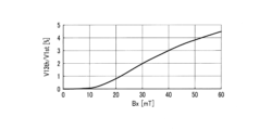
図10は、ギャップAGと磁界成分MFxとの関係の例を示す特性図である。図11は、ギャップAGと検出信号との関係の例を示す特性図である。図10および図11において、横軸はギャップAGを示している。図10において、縦軸は、磁気センサ2が検出し得る磁界成分MFxの最大の強度に対応する磁束密度Bxの大きさを示している。図11において、縦軸は、磁気センサ2に対する磁界発生器3の相対的な位置を変化させたときの第1の検出信号S1のピークピーク値Vppを示している。また、図10において、符号71を付した曲線は、1ピッチの大きさLpを1000μmとした磁界発生器3を用いたときの磁束密度Bxを示している。また、符号72を付した曲線は、1ピッチの大きさLpを750μmとした磁界発生器3を用いたときの磁束密度Bxを示している。
Figure 10 is a characteristic diagram showing an example of the relationship between the gap AG and the magnetic field component MFx. Figure 11 is a characteristic diagram showing an example of the relationship between the gap AG and the detection signal. In Figures 10 and 11, the horizontal axis indicates the gap AG. In Figure 10, the vertical axis indicates the magnitude of the magnetic flux density Bx corresponding to the maximum strength of the magnetic field component MFx that the
図10から理解されるように、磁束密度Bxすなわち磁界成分MFxの強度は、ギャップAGが大きくなるに従って小さくなる。また、図11から理解されるように、ピークピーク値Vppすなわち第1の検出信号S1の大きさは、ギャップAGが大きくなるに従って小さくなる。なお、図示しないが、ギャップAGと第1の検出信号S1との関係は、ギャップAGと第2の検出信号S2との関係にも当てはまる。従って、第2の検出信号S2も、ギャップAGが大きくなるに従って小さくなる。 As can be seen from FIG. 10, the magnetic flux density Bx, i.e., the strength of the magnetic field component MFx, decreases as the gap AG increases. Also, as can be seen from FIG. 11, the peak-to-peak value Vpp, i.e., the magnitude of the first detection signal S1, decreases as the gap AG increases. Although not shown, the relationship between the gap AG and the first detection signal S1 also applies to the relationship between the gap AG and the second detection signal S2. Therefore, the second detection signal S2 also decreases as the gap AG increases.
図12は、磁界成分MFxと検出信号との関係の例を示す特性図である。図12において、横軸は磁界成分MFxに対応する磁束密度Bxの大きさを示し、縦軸は第1の検出信号S1の大きさを示している。なお、図12では、磁界成分MFxの方向がX方向のときの磁束密度Bxを正の値で表し、磁界成分MFxの方向が-X方向のときの磁束密度Bxを負の値で表している。また、図12では、第1の検出信号S1の最大値が1になり、第1の検出信号S1の最小値が-1になるように、第1の検出信号S1を規格化している。 Figure 12 is a characteristic diagram showing an example of the relationship between the magnetic field component MFx and the detection signal. In Figure 12, the horizontal axis indicates the magnitude of the magnetic flux density Bx corresponding to the magnetic field component MFx, and the vertical axis indicates the magnitude of the first detection signal S1. In Figure 12, the magnetic flux density Bx is expressed as a positive value when the magnetic field component MFx is in the X direction, and the magnetic flux density Bx is expressed as a negative value when the magnetic field component MFx is in the -X direction. In Figure 12, the first detection signal S1 is normalized so that the maximum value of the first detection signal S1 is 1 and the minimum value of the first detection signal S1 is -1.
図12から理解されるように、磁界成分MFxの強度(磁束密度Bx)の変化の範囲が0を含み且つ比較的狭い場合(例えば、±7mT)には、第1の検出信号S1は、磁界成分MFxの強度の変化に対して大きく変化する。そのため、第1の検出信号S1の最大値も、磁界成分MFxの最大の強度の変化に対して大きく変化する。この場合、ギャップAGがずれて磁界成分MFxの最大の強度がずれると、第1の検出信号S1の最大値が大きく変動してしまう。 As can be seen from FIG. 12, when the range of change in the strength of the magnetic field component MFx (magnetic flux density Bx) includes 0 and is relatively narrow (e.g., ±7 mT), the first detection signal S1 changes significantly with respect to the change in the strength of the magnetic field component MFx. Therefore, the maximum value of the first detection signal S1 also changes significantly with respect to the change in the maximum strength of the magnetic field component MFx. In this case, if the gap AG shifts and the maximum strength of the magnetic field component MFx shifts, the maximum value of the first detection signal S1 will fluctuate significantly.
これに対し、本実施の形態では、第2の要件によって、MR素子50の各々に印加される磁界成分MFxの最大の強度を、バイアス磁界MFbの強度の1.2倍以上としている。これにより、本実施の形態では、第1の検出信号S1の変化の範囲を大きくして、第1の検出信号S1の最大値が、磁界成分MFxの最大の強度の変化に対して大きく変化しないようにしている。これにより、本実施の形態によれば、ギャップAGがずれて磁界成分MFxの最大の強度がずれたときの、第1の検出信号S1の最大値の変動を抑制することができる。
In contrast, in this embodiment, due to the second requirement, the maximum strength of the magnetic field component MFx applied to each
上記の第1の検出信号S1についての説明は、第2の検出信号S2にも当てはまる。本実施の形態によれば、第1の検出信号S1と同様に、ギャップAGがずれて磁界成分MFxの最大の強度がずれたときの、第2の検出信号S2の最大値の変動を抑制することができる。 The above explanation of the first detection signal S1 also applies to the second detection signal S2. According to this embodiment, as with the first detection signal S1, it is possible to suppress the fluctuation of the maximum value of the second detection signal S2 when the gap AG shifts and the maximum strength of the magnetic field component MFx shifts.
次に、第1および第2のシミュレーションの結果を参照して、磁界成分MFxの最大の強度とバイアス磁界MFbの強度との関係について詳しく説明する。なお、以下の説明において、磁界成分MFxの強度は、特に断りのない限り、磁界成分MFxの最大の強度である。 Next, the relationship between the maximum strength of the magnetic field component MFx and the strength of the bias magnetic field MFb will be described in detail with reference to the results of the first and second simulations. Note that in the following description, the strength of the magnetic field component MFx is the maximum strength of the magnetic field component MFx unless otherwise specified.
始めに、第1のシミュレーションについて説明する。第1のシミュレーションでは、磁気センサシステム1のモデルを用いた。磁界発生器3の1ピッチの大きさLpは、1000μmとした。
First, the first simulation will be described. In the first simulation, a model of the
第1のシミュレーションでは、ギャップAGを変化させることによって、ギャップAGと第1の検出信号S1のピークピーク値Vppとの関係を求めた。また、第1のシミュレーションでは、バイアス磁界MFbの強度に対応する磁束密度Bbを、0.1mT、2mT、5mT、10mT、15mTと変化させた。ギャップAGと第1の検出信号S1のピークピーク値Vppとの関係は、バイアス磁界MFbの強度毎(磁束密度Bb毎)に求めた。 In the first simulation, the gap AG was changed to obtain the relationship between the gap AG and the peak-to-peak value Vpp of the first detection signal S1. Also, in the first simulation, the magnetic flux density Bb corresponding to the strength of the bias magnetic field MFb was changed to 0.1 mT, 2 mT, 5 mT, 10 mT, and 15 mT. The relationship between the gap AG and the peak-to-peak value Vpp of the first detection signal S1 was obtained for each strength of the bias magnetic field MFb (each magnetic flux density Bb).
また、第1のシミュレーションでは、ギャップAGが変化したときの第1の検出信号S1の変動率(以下、出力変動率と言う。)を求めた。ここで、ギャップAGが第1の値のときのピークピーク値Vppを第1のピークピーク値と言い、ギャップAGが第1の値よりも50μm大きい第2の値のときのピークピーク値Vppを第2のピークピーク値と言う。第1のシミュレーションでは、第1のピークピーク値と第2のピークピーク値との差を、第1のピークピーク値で割った値を、ギャップAGが第1の値のときの出力変動率とした。そして、ギャップAGと磁界成分MFxの強度との関係から、磁界成分MFxの強度と出力変動率との関係を求めた。この関係は、バイアス磁界MFbの強度毎(磁束密度Bb毎)に求めた。 In the first simulation, the fluctuation rate of the first detection signal S1 when the gap AG changes (hereinafter referred to as the output fluctuation rate) was obtained. Here, the peak-peak value Vpp when the gap AG is at a first value is referred to as the first peak-peak value, and the peak-peak value Vpp when the gap AG is at a second value that is 50 μm larger than the first value is referred to as the second peak-peak value. In the first simulation, the difference between the first peak-peak value and the second peak-peak value divided by the first peak-peak value was used as the output fluctuation rate when the gap AG is at the first value. Then, the relationship between the strength of the magnetic field component MFx and the output fluctuation rate was obtained from the relationship between the gap AG and the strength of the magnetic field component MFx. This relationship was obtained for each strength of the bias magnetic field MFb (each magnetic flux density Bb).
図13は、ギャップAGと第1の検出信号S1のピークピーク値Vppとの関係を示す特性図である。図13において、横軸はギャップAGを示し、縦軸はピークピーク値Vppを示している。また、図13において、符号73で示す曲線は磁束密度Bbが0.1mTのときのピークピーク値Vppを示し、符号74で示す曲線は磁束密度Bbが2mTのときのピークピーク値Vppを示し、符号75で示す曲線は磁束密度Bbが5mTのときのピークピーク値Vppを示し、符号76で示す曲線は磁束密度Bbが10mTのときのピークピーク値Vppを示し、符号77で示す曲線は磁束密度Bbが15mTのときのピークピーク値Vppを示している。
Figure 13 is a characteristic diagram showing the relationship between the gap AG and the peak-peak value Vpp of the first detection signal S1. In Figure 13, the horizontal axis indicates the gap AG, and the vertical axis indicates the peak-peak value Vpp. Also, in Figure 13, the curve indicated by the
図13から、磁束密度Bbが0.1mTの場合以外の場合には、ピークピーク値Vppすなわち第1の検出信号S1の大きさは、ギャップAGが大きくなるに従って小さくなることが分かる。また、図13から、ギャップAGが変化したときの第1の検出信号S1の変化量は、バイアス磁界MFbの強度(磁束密度Bb)が小さくなるに従って小さくなることが分かる。 From Figure 13, it can be seen that except when the magnetic flux density Bb is 0.1 mT, the peak-to-peak value Vpp, i.e., the magnitude of the first detection signal S1, decreases as the gap AG increases. Also, from Figure 13, it can be seen that the amount of change in the first detection signal S1 when the gap AG changes decreases as the strength of the bias magnetic field MFb (magnetic flux density Bb) decreases.
図14は、磁界成分MFxの強度と出力変動率との関係を示す特性図である。図14において、横軸は磁界成分MFxの強度に対応する磁束密度Bxの大きさを示し、縦軸は出力変動率を示している。また、図14において、符号78で示す曲線は磁束密度Bbが2mTのときの出力変動率を示し、符号79で示す曲線は磁束密度Bbが5mTのときの出力変動率を示し、符号80で示す曲線は磁束密度Bbが10mTのときの出力変動率を示し、符号81で示す曲線は磁束密度Bbが15mTのときの出力変動率を示している。
Figure 14 is a characteristic diagram showing the relationship between the strength of the magnetic field component MFx and the output fluctuation rate. In Figure 14, the horizontal axis shows the magnitude of the magnetic flux density Bx corresponding to the strength of the magnetic field component MFx, and the vertical axis shows the output fluctuation rate. Also in Figure 14, the curve indicated by the
図14から、出力変動率は、磁界成分MFxの強度(磁束密度Bx)が大きくなるに従って小さくなることが分かる。また、図14から、出力変動率は、バイアス磁界MFbの強度(磁束密度Bb)が小さくなるに従って小さくなることが分かる。 From FIG. 14, it can be seen that the output fluctuation rate decreases as the strength of the magnetic field component MFx (magnetic flux density Bx) increases. Also, from FIG. 14, it can be seen that the output fluctuation rate decreases as the strength of the bias magnetic field MFb (magnetic flux density Bb) decreases.
第1のシミュレーションの結果から、磁界成分MFxの強度を大きくするか、バイアス磁界MFbの強度を小さくすることによって、出力変動率を小さくすることができることが分かる。検出信号の変動が小さいと判断できる出力変動率の上限値は、例えば15%である。図14から、出力変動率が15%になる磁束密度Bxは、磁束密度Bbが5mTの場合には6mTであり、磁束密度Bbが10mTの場合には12mTであり、磁束密度Bbが15mTの場合には18mTである。従って、磁束密度Bxが磁束密度Bbの1.2倍の場合に、出力変動率が15%になる。 The results of the first simulation show that the output fluctuation rate can be reduced by increasing the strength of the magnetic field component MFx or decreasing the strength of the bias magnetic field MFb. The upper limit of the output fluctuation rate at which it can be determined that the fluctuation of the detection signal is small is, for example, 15%. From FIG. 14, the magnetic flux density Bx at which the output fluctuation rate becomes 15% is 6 mT when the magnetic flux density Bb is 5 mT, 12 mT when the magnetic flux density Bb is 10 mT, and 18 mT when the magnetic flux density Bb is 15 mT. Therefore, when the magnetic flux density Bx is 1.2 times the magnetic flux density Bb, the output fluctuation rate becomes 15%.
磁束密度Bxは、MR素子50の各々に印加される磁界成分MFxの最大の強度に対応し、磁束密度Bbは、バイアス磁界MFbの強度に対応する。本実施の形態では、MR素子50の各々に印加される磁界成分MFxの最大の強度を、バイアス磁界MFbの強度の1.2倍以上にしている。これにより、本実施の形態によれば、出力変動率を15%以下にすることができる。
The magnetic flux density Bx corresponds to the maximum strength of the magnetic field component MFx applied to each
なお、出力変動率は、10%以下であることが好ましく、8%以下であることがより好ましい。図14から、出力変動率が10%になる磁束密度Bxは、磁束密度Bbが5mTの場合には8.5mTであり、磁束密度Bbが10mTの場合には17mTであり、磁束密度Bbが15mTの場合には25.5mTである。従って、磁束密度Bxが磁束密度Bbの1.7倍の場合に、出力変動率が10%になる。 The output fluctuation rate is preferably 10% or less, and more preferably 8% or less. From FIG. 14, the magnetic flux density Bx at which the output fluctuation rate becomes 10% is 8.5 mT when the magnetic flux density Bb is 5 mT, 17 mT when the magnetic flux density Bb is 10 mT, and 25.5 mT when the magnetic flux density Bb is 15 mT. Therefore, when the magnetic flux density Bx is 1.7 times the magnetic flux density Bb, the output fluctuation rate becomes 10%.
また、図14から、出力変動率が8%になる磁束密度Bxは、磁束密度Bbが5mTの場合には10mTであり、磁束密度Bbが10mTの場合には20mTであり、磁束密度Bbが15mTの場合には30mTである。従って、磁束密度Bxが磁束密度Bbの2倍の場合に、出力変動率が8%になる。 Also, from Figure 14, the magnetic flux density Bx at which the output fluctuation rate becomes 8% is 10 mT when the magnetic flux density Bb is 5 mT, 20 mT when the magnetic flux density Bb is 10 mT, and 30 mT when the magnetic flux density Bb is 15 mT. Therefore, when the magnetic flux density Bx is twice the magnetic flux density Bb, the output fluctuation rate becomes 8%.
以上のことから、MR素子50の各々に印加される磁界成分MFxの最大の強度は、バイアス磁界MFbの強度の1.7倍以上であることが好ましく、2倍以上であることがより好ましい。
For the above reasons, the maximum strength of the magnetic field component MFx applied to each
次に、第2のシミュレーションについて説明する。第2のシミュレーションでは、第1のシミュレーションと同様に、磁気センサシステム1のモデルを用いた。なお、バイアス磁界MFbに対応する磁束密度Bbは、5mTとした。
Next, the second simulation will be described. In the second simulation, a model of the
ここで、MR素子50の各々に印加される磁界成分MFxの最大の強度の、バイアス磁界MFbの強度に対する倍率を、磁界倍率と言う。第2のシミュレーションでは、磁界成分MFxの強度を変化させることによって、磁界倍率が、検出信号および検出値Vsに与える影響について調べた。具体的には、第1の検出信号S1の誤差成分に含まれる、理想成分の第13高調波(13次の高調波)に相当する成分を求め、磁界成分MFxの強度と第13高調波との関係を求めた。
Here, the magnification of the maximum strength of the magnetic field component MFx applied to each
また、第2のシミュレーションでは、第1および第2の検出信号S1,S2から前述の初期検出値を求めた。また、第1および第2の検出信号S1,S2の各々の理想成分から初期検出値に相当する理想角度を求めると共に、初期検出値と理想角度との差(以下、角度誤差と言う。)を求めた。そして、磁界倍率と角度誤差との関係を求めた。 In the second simulation, the aforementioned initial detection value was obtained from the first and second detection signals S1 and S2. The ideal angle corresponding to the initial detection value was obtained from each ideal component of the first and second detection signals S1 and S2, and the difference between the initial detection value and the ideal angle (hereinafter referred to as the angle error) was obtained. Then, the relationship between the magnetic field magnification and the angle error was obtained.
図15は、磁界成分MFxの強度と第13高調波との関係を示す特性図である。図15において、横軸は、磁界成分MFxの強度に対応する磁束密度Bxを示している。また、図15において、縦軸は、第13高調波の振幅の理想成分の振幅に対する比率V13th/V1stを示している。図15から、比率V13th/V1stは、磁束密度Bxが大きくなるに従って大きくなることが分かる。この結果から、磁界倍率が大きくなると、第13高調波の振幅が大きくなることが分かる。 Figure 15 is a characteristic diagram showing the relationship between the strength of the magnetic field component MFx and the 13th harmonic. In Figure 15, the horizontal axis shows the magnetic flux density Bx corresponding to the strength of the magnetic field component MFx. Also, in Figure 15, the vertical axis shows the ratio V13th/V1st of the amplitude of the 13th harmonic to the amplitude of the ideal component. From Figure 15, it can be seen that the ratio V13th/V1st increases as the magnetic flux density Bx increases. From this result, it can be seen that as the magnetic field magnification increases, the amplitude of the 13th harmonic increases.
磁気センサシステム1の磁気センサ2では、誤差成分に含まれる、11次以下の奇数次の高調波に相当する成分が低減されるように、複数のMR素子50が配置されている。言い換えると、磁気センサ2は、誤差成分に含まれる、13次以上の高調波に相当する成分が低減されるようには構成されていない。そのため、図15に示したように、磁束密度Bxが大きくなると、第13高調波の振幅が大きくなる。従って、磁界倍率が大きくなると、誤差成分に含まれる第13高調波に相当する成分が大きくなる。
In the
図16は、磁界倍率と角度誤差との関係を示す特性図である。図16において、横軸は磁界倍率を示し、縦軸は角度誤差を示している。図16から、磁界倍率が大きくなると、角度誤差が大きくなることが分かる。これは、前述のように、磁界倍率が大きくなると、誤差成分のうちの第13高調波に相当する成分が大きくなるからである。 Figure 16 is a characteristic diagram showing the relationship between magnetic field magnification and angular error. In Figure 16, the horizontal axis shows magnetic field magnification, and the vertical axis shows angular error. From Figure 16, it can be seen that as the magnetic field magnification increases, the angular error increases. This is because, as mentioned above, as the magnetic field magnification increases, the component of the error component that corresponds to the 13th harmonic increases.
角度誤差が大きくなると、検出値Vsの誤差が大きくなる。従って、図16から、磁界倍率が大きくなると、検出値Vsの誤差が大きくなることが分かる。 As the angle error increases, the error in the detection value Vs also increases. Therefore, from Figure 16, it can be seen that as the magnetic field magnification increases, the error in the detection value Vs also increases.
検出値Vsの誤差を許容できる角度誤差の上限値は、例えば3°である。図16から、角度誤差が3°となる磁界倍率は15.6である。磁界倍率は、MR素子50の各々に印加される磁界成分MFxの最大の強度の、バイアス磁界MFbの強度に対する倍率に対応する。従って、MR素子50の各々に印加される磁界成分MFxの最大の強度を、バイアス磁界MFbの強度の15.6倍以下にすることにより、角度誤差を3°以下にすることができる。
The upper limit of the angle error that allows for an error in the detection value Vs is, for example, 3°. From FIG. 16, the magnetic field magnification at which the angle error is 3° is 15.6. The magnetic field magnification corresponds to the magnification of the maximum strength of the magnetic field component MFx applied to each of the
なお、角度誤差は、2°以下であることが好ましく、1°以下であることがより好ましい。図16から、角度誤差が2°になる磁界倍率は9.2であり、角度誤差が1°になる磁界倍率は5.6である。従って、MR素子50の各々に印加される磁界成分MFxの最大の強度は、バイアス磁界MFbの強度の9.2倍以下であることが好ましく、5.6倍以下であることがより好ましい。
The angular error is preferably 2° or less, and more preferably 1° or less. From FIG. 16, the magnetic field magnification at which the angular error is 2° is 9.2, and the magnetic field magnification at which the angular error is 1° is 5.6. Therefore, the maximum strength of the magnetic field component MFx applied to each
ところで、本実施の形態では、磁気センサシステム1には、検出値生成回路4が設けられている。本実施の形態における磁気センサ2を用いる場合、検出値生成回路4または演算回路47において、第1および第2の検出信号S1,S2または検出値Vsを補正して、角度誤差に起因する誤差を低減することができる。上述のように、角度誤差がある程度小さくなるような磁界倍率にしておくことにより、第1および第2の検出信号S1,S2または検出値Vsの補正が容易になる。
In the present embodiment, the
次に、第3のシミュレーションの結果を参照して、バイアス磁界MFbの強度について説明する。第3のシミュレーションでは、第1および第2のシミュレーションと同様に、磁気センサシステム1のモデルを用いた。
Next, the strength of the bias magnetic field MFb will be described with reference to the results of the third simulation. In the third simulation, the model of the
第3のシミュレーションでは、バイアス磁界MFbの強度を変化させたときの、磁界成分MFxと検出信号との関係を求めた。第3のシミュレーションでは、検出信号として、第1の検出信号S1を用いた。また、第3のシミュレーションでは、バイアス磁界MFbの強度に対応する磁束密度Bbを、0mT、2mT、5mT、8mT、10mT、15mT、20mTと変化させた。磁界成分MFxと第1の検出信号S1との関係は、バイアス磁界MFbの強度毎(磁束密度Bb毎)に求めた。 In the third simulation, the relationship between the magnetic field component MFx and the detection signal was obtained when the strength of the bias magnetic field MFb was changed. In the third simulation, the first detection signal S1 was used as the detection signal. In the third simulation, the magnetic flux density Bb corresponding to the strength of the bias magnetic field MFb was changed to 0 mT, 2 mT, 5 mT, 8 mT, 10 mT, 15 mT, and 20 mT. The relationship between the magnetic field component MFx and the first detection signal S1 was obtained for each strength of the bias magnetic field MFb (each magnetic flux density Bb).
図17は、磁界成分MFxと第1の検出信号S1との関係を示す特性図である。図17において、横軸は磁界成分MFxの強度に対応する磁束密度Bxを示し、縦軸は第1の検出信号S1を示している。また、図17において、符号82で示す曲線は磁束密度Bbが0mTのときの第1の検出信号S1を示し、符号83で示す曲線は磁束密度Bbが2mTのときの第1の検出信号S1を示し、符号84で示す曲線は磁束密度Bbが5mTのときの第1の検出信号S1を示し、符号85で示す曲線は磁束密度Bbが8mTのときの第1の検出信号S1を示し、符号86で示す曲線は磁束密度Bbが10mTのときの第1の検出信号S1を示し、符号87で示す曲線は磁束密度Bbが15mTのときの第1の検出信号S1を示し、符号88で示す曲線は磁束密度Bbが20mTのときの第1の検出信号S1を示している。
Figure 17 is a characteristic diagram showing the relationship between the magnetic field component MFx and the first detection signal S1. In Figure 17, the horizontal axis shows the magnetic flux density Bx corresponding to the strength of the magnetic field component MFx, and the vertical axis shows the first detection signal S1. In FIG. 17, the curve indicated by the
図17に示した例では、磁束密度Bxが0のときの第1の検出信号S1(第1の検出信号S1のオフセット)は、理想的には、1.4Vである。ここで、磁束密度Bxを負の値から大きくしたときに第1の検出信号S1が1.4Vとなる磁束密度Bxの値を第1の値と言い、磁束密度Bxを正の値から小さくしたときに第1の検出信号S1が1.4Vとなる磁束密度Bxの値を第2の値と言う。また、第1の値と第2の値の差の絶対値を、ヒステリシスHysと言う。 In the example shown in FIG. 17, the first detection signal S1 (offset of the first detection signal S1) when the magnetic flux density Bx is 0 is ideally 1.4 V. Here, the value of magnetic flux density Bx at which the first detection signal S1 becomes 1.4 V when the magnetic flux density Bx is increased from a negative value is called the first value, and the value of magnetic flux density Bx at which the first detection signal S1 becomes 1.4 V when the magnetic flux density Bx is decreased from a positive value is called the second value. The absolute value of the difference between the first value and the second value is called the hysteresis Hys.
図18は、バイアス磁界MFbとヒステリシスHysとの関係を示す特性図である。図18において、横軸はバイアス磁界MFbの強度に対応する磁束密度Bbを示し、縦軸はヒステリシスHysを示している。図18から、ヒステリシスHysは、バイアス磁界MFbの強度(磁束密度Bb)が小さくなるに従って小さくなることが分かる。 Figure 18 is a characteristic diagram showing the relationship between the bias magnetic field MFb and hysteresis Hys. In Figure 18, the horizontal axis shows the magnetic flux density Bb corresponding to the strength of the bias magnetic field MFb, and the vertical axis shows the hysteresis Hys. From Figure 18, it can be seen that the hysteresis Hys decreases as the strength of the bias magnetic field MFb (magnetic flux density Bb) decreases.
検出値Vsの誤差は、前述の角度誤差の他、ヒステリシスHysに起因しても生じる。検出値Vsの誤差を許容できるヒステリシスHysの上限値は、例えば1mTである。図18から、ヒステリシスHysが1mTとなる磁束密度Bbは3mTである。従って、バイアス磁界MFbの強度に対応する磁束密度Bbは、3mT以上であることが好ましい。 In addition to the angle error mentioned above, errors in the detection value Vs are also caused by hysteresis Hys. The upper limit of hysteresis Hys that allows for an error in the detection value Vs is, for example, 1 mT. From FIG. 18, the magnetic flux density Bb at which the hysteresis Hys becomes 1 mT is 3 mT. Therefore, it is preferable that the magnetic flux density Bb corresponding to the strength of the bias magnetic field MFb is 3 mT or more.
なお、バイアス磁界MFbの強度を大きくすると、出力変動率を小さくするために、磁界成分MFxの強度を大きくする必要がある。磁界成分MFxの強度を大きくするためには、例えばギャップAGを小さくする必要がある。ギャップAGをある程度大きくする観点から、バイアス磁界MFbの強度に対応する磁束密度Bbは、40mT以下であることが好ましい。 When the strength of the bias magnetic field MFb is increased, the strength of the magnetic field component MFx must be increased in order to reduce the output fluctuation rate. In order to increase the strength of the magnetic field component MFx, for example, it is necessary to reduce the gap AG. From the viewpoint of increasing the gap AG to a certain extent, it is preferable that the magnetic flux density Bb corresponding to the strength of the bias magnetic field MFb is 40 mT or less.
ところで、バイアス磁界MFbは、バイアス磁界発生器50Bが発生する外部磁界と、MR素子50の自由層53が有する異方性に起因する異方性磁界の、一方または両方によるものである。バイアス磁界発生器50Bとして磁石対50C(第1および第2の磁石54,55)を設けた場合、バイアス磁界MFbの方向を1つの方向(Y方向または-Y方向)にすることができる。磁界成分MFxの強度が0のときの第1および第2の検出信号S1,S2の各々の大きさすなわちオフセットは、自由層53の磁化の向きがY方向であるか-Y方向であるかで異なり得る。これに対し、磁石対50C(第1および第2の磁石54,55)を設けることによって、磁界成分MFxの強度が0のときの自由層53の磁化の向きを1つの方向(Y方向または-Y方向)に固定することができる。これにより、オフセットの補正が容易になる。
The bias magnetic field MFb is generated by one or both of the external magnetic field generated by the bias
また、バイアス磁界発生器50Bによる外部磁界の強度をある程度大きくすることにより、外部磁界の方向とは反対方向の磁界がMR素子50に印加された場合に、磁界成分MFxの強度が0のときの自由層53の磁化の向きが反転して、オフセットが変動することを防止することができる。このような観点からも、バイアス磁界MFbの強度に対応する磁束密度Bbは、ある程度大きいこと、具体的には3mT以上であることが好ましい。
In addition, by increasing the strength of the external magnetic field generated by the bias
次に、本実施の形態におけるその他の効果について説明する。本実施の形態では、第1および第2の検出信号S1,S2の各々の誤差成分に含まれる、11次以下の奇数次の高調波に相当する成分が低減されるように、複数のMR素子50が配置されている。第2のシミュレーションの結果から理解されるように、磁界倍率、具体的には磁界成分MFxの強度が大きくなるに従って、誤差成分に含まれる、13次の高調波に相当する成分が大きくなる。もし、複数のMR素子50が上記のように配置されていないと、磁界成分MFxの強度が大きくなるに従って、11次以下の奇数次の高調波に相当する成分も大きくなる。この場合、第1および第2の検出信号S1,S2の波形は、矩形波状に歪む。その結果、検出値Vsの誤差は大きくなる。
Next, other effects of this embodiment will be described. In this embodiment, the
これに対し、本実施の形態によれば、複数のMR素子50を上記のように配置することにより、磁界成分MFxの強度が大きくしながら、第1および第2の検出信号S1,S2の各々に含まれる誤差成分を低減して、第1および第2の検出信号S1,S2の各々の波形を理想的な正弦曲線に近づけることができる。その結果、本実施の形態によれば、出力変動率を小さくしながら、検出値Vsの誤差を小さくすることができる。
In contrast, according to the present embodiment, by arranging
次に、図19および図20を参照して、本実施の形態に係るレンズ位置検出装置(以下、単に位置検出装置と記す。)について説明する。図19は、本実施の形態に係る位置検出装置を含むレンズモジュールを示す斜視図である。図20は、本実施の形態に係る位置検出装置を示す斜視図である。 Next, a lens position detection device (hereinafter simply referred to as a position detection device) according to this embodiment will be described with reference to Fig. 19 and Fig . 20. Fig. 19 is a perspective view showing a lens module including a position detection device according to this embodiment. Fig. 20 is a perspective view showing a position detection device according to this embodiment.
図19に示したレンズモジュール300は、例えばスマートフォン用のカメラの一部を構成するものであり、CMOS等を用いたイメージセンサ310と組み合わせて用いられる。図19に示した例では、レンズモジュール300は、三角柱形状のプリズム302と、イメージセンサ310とプリズム302との間に設けられた3つのレンズ303A,303B,303Cとを備えている。レンズ303A,303B,303Cのうちの少なくとも1つは、焦点合わせとズームの少なくとも一方を行うことができるように、図示しない駆動装置によって移動可能に構成されている。
The
図20には、レンズ303A,303B,303Cのうちの任意のレンズ303を示している。レンズモジュール300は、更に、レンズ303を保持するレンズホルダ304と、シャフト305とを備えている。レンズモジュール300では、レンズホルダ304と、シャフト305と、図示しない駆動装置によって、レンズ303の位置が、レンズ303の光軸方向に変化可能になっている。図20において、記号Dを付した矢印は、レンズ303の移動方向を示している。
Figure 20 shows an
レンズモジュール300は、更に、位置が変化可能なレンズ303の位置を検出するための位置検出装置301を備えている。位置検出装置301は、焦点合わせまたはズームを行う際に、レンズ303の位置を検出するために用いられる。
The
位置検出装置301は、磁気式の位置検出装置であり、本実施の形態に係る磁気センサシステム1を備えている。レンズモジュール300では、磁気センサシステム1の磁気センサ2と磁界発生器3は、レンズ303の位置が移動方向Dに変化すると、磁界成分MFx(図2参照)の強度が変化するように構成されている。具体的には、磁気センサ2が固定されて、磁界発生器3がレンズ303と共に移動方向Dに移動可能に構成されている。移動方向Dは、図1および図2に示したX方向に平行になる。これにより、レンズ303の位置が変化すると、磁気センサ2に対する磁界発生器3の相対的な位置が変化し、その結果、磁界成分MFxの強度が変化する。
The
位置検出装置301は、更に、本実施の形態における検出値生成回路4(図3参照)を備えている。位置検出装置301では、磁気センサ2が生成する第1および第2の検出信号S1,S2に基づいて、レンズ303の位置と対応関係を有する検出値Vsを生成する。なお、レンズ303の位置は、磁気センサ2に対する磁界発生器3の相対的な位置と対応関係を有している。位置検出装置301における検出値Vsの生成方法は、前述の検出値Vsの生成方法と同様である。
The
[変形例]
次に、本実施の形態におけるMR素子50の変形例について説明する。始めに、図21を参照して、MR素子50の第1の変形例について説明する。第1の変形例では、複数の軟磁性層50Eのうちの2つの軟磁性層50Eが、Z方向から見て同じMR素子50と重なる位置に配置されている。この2つの軟磁性層50Eは、X方向に並ぶと共に、所定の間隔を開けて配置されている。2つの軟磁性層50Eの一方は、積層膜50Aの-X方向の端の近傍に位置する。2つの軟磁性層50Eの他方は、積層膜50AのX方向の端の近傍に位置する。2つの軟磁性層50Eは、積層膜50Aと磁石対50C(第1および第2の磁石54,55)との間に配置されている。2つの軟磁性層50Eの各々は、Y方向に長い平面形状を有している。
[Modification]
Next, modified examples of the
次に、図22を参照して、MR素子50の第2の変形例について説明する。第2の変形例では、MR素子50は、図7および図8に示した積層膜50Aの代わりに、2つの積層膜50A1,50A2を含んでいる。積層膜50A1,50A2の各々の構成は、積層膜50Aの構成と同じである。積層膜50A1,50A2は、電極によって並列に接続されて、積層膜対を構成する。積層膜対は、電極によって、他のMR素子50の積層膜対に対して直列に接続されている。例えば、積層膜50A1,50A2の各々の下面は、図示しない下部電極によって、他のMR素子50の積層膜50A1,50A2の各々の下面に電気的に接続され、積層膜50A1,50A2の各々の上面は、図示しない上部電極によって、更に他のMR素子50の積層膜50A1,50A2の各々の上面に電気的に接続される。
Next, a second modified example of the
第2の変形例では、磁石対50Cの第1の磁石54は、積層膜50A1,50A2の各々の-Y方向の端の近傍に位置する。第2の磁石55は、積層膜50A1,50A2の各々のY方向の端の近傍に位置する。軟磁性層50Eは、Z方向から見て積層膜50A1と積層膜50A2の両方と重なる位置に配置されている。
In the second modified example, the
MR素子50、磁石対50Cおよび軟磁性層50Eの構成は、図7、図8、図21および図22に示した例に限られない。例えば、1つのMR素子50に含まれる積層膜の数は、図7、図8および図21に示した例では1個であり、図22に示した例では2個である。しかし、積層膜の数は3個以上であってもよい。また、1つのMR素子50に重なる軟磁性層50Eの数は、図7、図8および図22に示した例では1個であり、図21に示した例では2個である。しかし、軟磁性層50Eの数は、3個以上であってもよいし、0個であってもよい。
The configurations of the
以下、複数の積層膜がX方向に沿って並び、複数の軟磁性層50EがX方向に沿って並ぶ場合を例にとって説明する。例えば、積層膜の数が2個であり軟磁性層50Eの数が2個の場合、1個目の軟磁性層50Eは、Z方向から見て1個目の積層膜と重なる位置に配置され、2個目の軟磁性層50Eは、Z方向から見て2個目の積層膜と重なる位置に配置されていてもよい。
Below, an example will be described in which multiple laminated films are arranged along the X direction, and multiple soft
また、積層膜の数が2個であり軟磁性層50Eの数が3個の場合、1個目の軟磁性層50Eは、Z方向から見て1個目の積層膜のみと重なる位置に配置され、2個目の軟磁性層50Eは、Z方向から見て1個目の積層膜と2個目の積層膜の両方と重なる位置に配置され、3個目の軟磁性層50Eは、Z方向から見て2個目の積層膜のみと重なる位置に配置されていてもよい。
In addition, when the number of laminated films is two and the number of soft
また、積層膜の数が3個であり軟磁性層50Eの数が2個の場合、1個目の軟磁性層50Eは、Z方向から見て1個目の積層膜と2個目の積層膜の両方と重なる位置に配置され、2個目の軟磁性層50Eは、Z方向から見て2個目の積層膜と3個目の積層膜の両方と重なる位置に配置されていてもよい。
Also, when the number of laminated films is three and the number of soft
また、積層膜の数が3個であり軟磁性層50Eの数が4個の場合、1個目の軟磁性層50Eは、Z方向から見て1個目の積層膜のみと重なる位置に配置され、2個目の軟磁性層50Eは、Z方向から見て1個目の積層膜と2個目の積層膜の両方と重なる位置に配置され、3個目の軟磁性層50Eは、Z方向から見て2個目の積層膜と3個目の積層膜の両方と重なる位置に配置され、4個目の軟磁性層50Eは、Z方向から見て3個目の積層膜のみと重なる位置に配置されていてもよい。
Also, when the number of laminated films is three and the number of soft
なお、本発明は、上記実施の形態に限定されず、種々の変更が可能である。例えば、請求の範囲の要件を満たす限り、MR素子50の形状、数および配置は、各実施の形態に示した例に限られず、任意である。MR素子50の平面形状は、矩形に限らず、円形、楕円形等であってもよい。
The present invention is not limited to the above-described embodiments, and various modifications are possible. For example, as long as the requirements of the claims are met, the shape, number, and arrangement of the
また、各抵抗体は、図6に示した素子群501~516のうち、素子群501~504,509~512のみを有していてもよい。これにより、誤差成分に含まれる、7次以下の奇数次の高調波に相当する成分を低減することができる。
In addition, each resistor may have
また、磁界発生器3は、回転方向に複数組のN極とS極を着磁した回転スケールであってもよい。回転スケールは、リング状磁石であってもよいし、磁気テープ等の磁気媒体をリングまたは円板に固定したものであってもよい。
The
1…磁気センサシステム、2…磁気センサ、3…磁界発生器、4…検出値生成回路、10…基板、11~14…端子、50…MR素子、50A…積層膜、50B…バイアス磁界発生器、50C…磁石対、50D…磁界増幅器、50E…軟磁性層、51…磁化固定層、52…ギャップ層、53…自由層、54…第1の磁石、55…第2の磁石、300…レンズモジュール、301…位置検出装置、302…プリズム、303,303A~303C…レンズ、304…レンズホルダ、305…シャフト、310…イメージセンサ、501~516…素子群、MF…対象磁界、MFb…バイアス磁界、MFx…磁界成分。 1...magnetic sensor system, 2...magnetic sensor, 3...magnetic field generator, 4...detection value generating circuit, 10...substrate, 11-14...terminals, 50...MR element, 50A...laminated film, 50B...bias magnetic field generator, 50C...magnet pair, 50D...magnetic field amplifier, 50E...soft magnetic layer, 51...magnetization fixed layer, 52...gap layer, 53...free layer, 54...first magnet, 55...second magnet, 300...lens module, 301...position detection device, 302...prism, 303, 303A-303C...lens, 304...lens holder, 305...shaft, 310...image sensor, 501-516...element group, MF...target magnetic field, MFb...bias magnetic field, MFx...magnetic field component.
Claims (11)
前記対象磁界を検出する磁気センサとを備え、
前記磁気センサと前記磁界発生器は、前記磁気センサに対する前記磁界発生器の相対的な位置が変化すると、前記磁気センサが検出する前記対象磁界の、第1の方向の磁界成分の強度が変化するように構成され、
前記磁気センサは、複数の磁気抵抗効果素子を含み、
前記複数の磁気抵抗効果素子の各々は、方向が固定された磁化を有する磁化固定層と、前記磁界成分の方向および強度に応じて方向が変化可能な磁化を有する自由層と、前記磁化固定層と前記自由層の間に配置されたギャップ層とを含み、前記第1の方向に直交する第2の方向のバイアス磁界が前記自由層に印加されるように構成されると共に前記磁界成分の強度に応じて抵抗値が変化するように構成され、
前記複数の磁気抵抗効果素子の各々に印加される前記磁界成分の最大の強度は、前記バイアス磁界の強度の1.2倍以上であることを特徴とする磁気センサシステム。 a magnetic field generator for generating a target magnetic field;
A magnetic sensor for detecting the target magnetic field,
the magnetic sensor and the magnetic field generator are configured such that a strength of a magnetic field component in a first direction of the target magnetic field detected by the magnetic sensor changes when a relative position of the magnetic field generator with respect to the magnetic sensor changes;
the magnetic sensor includes a plurality of magnetoresistance effect elements;
Each of the plurality of magnetoresistance effect elements includes a magnetization fixed layer having a magnetization whose direction is fixed, a free layer having a magnetization whose direction is changeable according to the direction and strength of the magnetic field component, and a gap layer disposed between the magnetization fixed layer and the free layer, and is configured such that a bias magnetic field in a second direction perpendicular to the first direction is applied to the free layer, and a resistance value changes according to the strength of the magnetic field component;
A magnetic sensor system, characterized in that a maximum intensity of the magnetic field component applied to each of the plurality of magnetoresistance effect elements is 1.2 times or more the intensity of the bias magnetic field.
前記バイアス磁界は、少なくとも、前記外部磁界によるものであることを特徴とする請求項1または2記載の磁気センサシステム。 The magnetic sensor further includes a bias magnetic field generator that generates an external magnetic field applied to the free layer;
3. The magnetic sensor system according to claim 1, wherein the bias magnetic field is generated by at least the external magnetic field.
前記複数の磁石対の各々において、前記第1の磁石と前記第2の磁石は、前記複数の磁気抵抗効果素子のうちの少なくとも1つの磁気抵抗効果素子の前記自由層の全体に前記外部磁界が印加されるように、前記第2の方向について所定の間隔を開けて配置されていることを特徴とする請求項4記載の磁気センサシステム。 the bias magnetic field generator includes a plurality of magnet pairs, each of which includes a first magnet and a second magnet;
The magnetic sensor system of claim 4, characterized in that in each of the multiple magnet pairs, the first magnet and the second magnet are arranged at a predetermined interval in the second direction so that the external magnetic field is applied to the entire free layer of at least one magnetoresistive element among the multiple magnetoresistive elements.
前記バイアス磁界は、少なくとも、前記形状磁気異方性によるものであることを特徴とする請求項1または2記載の磁気センサシステム。 the free layer has a shape magnetic anisotropy;
3. The magnetic sensor system according to claim 1, wherein the bias magnetic field is due to at least the shape magnetic anisotropy.
請求項1ないし8のいずれかに記載の磁気センサシステムを備え、
前記レンズは、前記第1の方向に移動可能に構成され、
前記磁気センサと前記磁界発生器は、前記レンズの位置が変化すると、前記磁界成分の強度が変化するように構成されていることを特徴とするレンズ位置検出装置。 A lens position detection device for detecting a position of a lens whose position can be changed, comprising:
A magnetic sensor system according to any one of claims 1 to 8 ,
The lens is configured to be movable in the first direction;
A lens position detection device, characterized in that the magnetic sensor and the magnetic field generator are configured so that the strength of the magnetic field component changes when the position of the lens changes.
Priority Applications (5)
| Application Number | Priority Date | Filing Date | Title |
|---|---|---|---|
| JP2020132658A JP7534146B2 (en) | 2020-08-04 | 2020-08-04 | Magnetic sensor system and lens position detection device |
| US17/384,939 US11486734B2 (en) | 2020-08-04 | 2021-07-26 | Magnetic sensor system and lens position detection device |
| DE102021119395.8A DE102021119395A1 (en) | 2020-08-04 | 2021-07-27 | MAGNETIC SENSING SYSTEM AND LENS POSITION DETECTION DEVICE |
| CN202110891138.5A CN114063172B (en) | 2020-08-04 | 2021-08-04 | Magnetic sensor system and lens position detection device |
| JP2023062795A JP7463593B2 (en) | 2020-08-04 | 2023-04-07 | Magnetic sensor system and lens position detection device |
Applications Claiming Priority (1)
| Application Number | Priority Date | Filing Date | Title |
|---|---|---|---|
| JP2020132658A JP7534146B2 (en) | 2020-08-04 | 2020-08-04 | Magnetic sensor system and lens position detection device |
Related Child Applications (1)
| Application Number | Title | Priority Date | Filing Date |
|---|---|---|---|
| JP2023062795A Division JP7463593B2 (en) | 2020-08-04 | 2023-04-07 | Magnetic sensor system and lens position detection device |
Publications (2)
| Publication Number | Publication Date |
|---|---|
| JP2022029354A JP2022029354A (en) | 2022-02-17 |
| JP7534146B2 true JP7534146B2 (en) | 2024-08-14 |
Family
ID=79686144
Family Applications (2)
| Application Number | Title | Priority Date | Filing Date |
|---|---|---|---|
| JP2020132658A Active JP7534146B2 (en) | 2020-08-04 | 2020-08-04 | Magnetic sensor system and lens position detection device |
| JP2023062795A Active JP7463593B2 (en) | 2020-08-04 | 2023-04-07 | Magnetic sensor system and lens position detection device |
Family Applications After (1)
| Application Number | Title | Priority Date | Filing Date |
|---|---|---|---|
| JP2023062795A Active JP7463593B2 (en) | 2020-08-04 | 2023-04-07 | Magnetic sensor system and lens position detection device |
Country Status (4)
| Country | Link |
|---|---|
| US (1) | US11486734B2 (en) |
| JP (2) | JP7534146B2 (en) |
| CN (1) | CN114063172B (en) |
| DE (1) | DE102021119395A1 (en) |
Families Citing this family (1)
| Publication number | Priority date | Publication date | Assignee | Title |
|---|---|---|---|---|
| CN114845023B (en) * | 2022-04-26 | 2024-09-20 | 杭州海康威视数字技术股份有限公司 | Driving method and device |
Citations (6)
| Publication number | Priority date | Publication date | Assignee | Title |
|---|---|---|---|---|
| JP2012122792A (en) | 2010-12-07 | 2012-06-28 | Alps Electric Co Ltd | Magnetic sensor |
| JP2016130686A (en) | 2015-01-14 | 2016-07-21 | Tdk株式会社 | Magnetic sensor |
| JP2016176911A (en) | 2015-03-23 | 2016-10-06 | Tdk株式会社 | Magnetic sensor |
| JP2017103378A (en) | 2015-12-03 | 2017-06-08 | ヤマハ株式会社 | Magnetoresistance effect element, magnetic sensor, manufacturing method of magnetoresistance effect element, and manufacturing method of magnetic sensor |
| JP2017227825A (en) | 2016-06-24 | 2017-12-28 | オリンパス株式会社 | Lens drive device and lens drive control method |
| WO2018190261A1 (en) | 2017-04-12 | 2018-10-18 | Tdk株式会社 | Magnetic sensor |
Family Cites Families (21)
| Publication number | Priority date | Publication date | Assignee | Title |
|---|---|---|---|---|
| JPS627834A (en) | 1985-07-03 | 1987-01-14 | Furukawa Alum Co Ltd | Manufacture of aluminum alloy plate |
| JP3123276B2 (en) | 1993-01-12 | 2001-01-09 | ソニー・プレシジョン・テクノロジー株式会社 | Position detection device |
| CN100554885C (en) * | 2005-04-19 | 2009-10-28 | 松下电器产业株式会社 | Position transducer, optical-head apparatus, head moving mechanism and position control system |
| DE112007003025T5 (en) | 2006-12-13 | 2009-11-12 | Alps Electric Co., Ltd. | Magnetic sensor and magnetic encoder that uses it |
| JP4458103B2 (en) * | 2007-02-27 | 2010-04-28 | Tdk株式会社 | Magnetic sensor, magnetic direction sensor, magnetic field detection method, and magnetic direction detection method |
| JP5295163B2 (en) * | 2010-04-01 | 2013-09-18 | 三菱電機株式会社 | Magnetic field detection apparatus and method for adjusting the same |
| US20120068698A1 (en) * | 2010-09-17 | 2012-03-22 | Industrial Technology Research Institute | Structure of tmr and fabrication method of integrated 3-axis magnetic field sensor and sensing circuit |
| JP5533826B2 (en) * | 2011-09-19 | 2014-06-25 | 株式会社デンソー | Current sensor and current sensor assembly structure |
| JP5532166B1 (en) * | 2013-03-29 | 2014-06-25 | Tdk株式会社 | Magnetic sensor and magnetic sensor system |
| JP5843079B2 (en) * | 2013-03-29 | 2016-01-13 | Tdk株式会社 | Magnetic sensor and magnetic sensor system |
| US9733317B2 (en) | 2014-03-10 | 2017-08-15 | Dmg Mori Seiki Co., Ltd. | Position detecting device |
| JP6548357B2 (en) * | 2014-03-28 | 2019-07-24 | Dmg森精機株式会社 | Position detection device |
| JP6472175B2 (en) | 2014-06-09 | 2019-02-20 | Dmg森精機株式会社 | Position detection device |
| JP6601079B2 (en) * | 2015-09-11 | 2019-11-06 | 凸版印刷株式会社 | Magnetic sensor |
| JP6331176B1 (en) * | 2017-03-24 | 2018-05-30 | Tdk株式会社 | Angle sensor system |
| JP6490130B2 (en) * | 2017-03-24 | 2019-03-27 | Tdk株式会社 | Magnetic sensor |
| JP6687046B2 (en) * | 2018-02-16 | 2020-04-22 | Tdk株式会社 | Magnetic sensor system and magnetic scale |
| JP6597820B2 (en) * | 2018-03-12 | 2019-10-30 | Tdk株式会社 | Magnetic sensor and position detection device |
| JP6620834B2 (en) * | 2018-03-27 | 2019-12-18 | Tdk株式会社 | Magnetic sensor and magnetic sensor system |
| JP2019211385A (en) * | 2018-06-07 | 2019-12-12 | 矢崎総業株式会社 | Magnetic detection device and magnetic bias device |
| JP6954327B2 (en) * | 2019-06-10 | 2021-10-27 | Tdk株式会社 | Position detector |
-
2020
- 2020-08-04 JP JP2020132658A patent/JP7534146B2/en active Active
-
2021
- 2021-07-26 US US17/384,939 patent/US11486734B2/en active Active
- 2021-07-27 DE DE102021119395.8A patent/DE102021119395A1/en active Pending
- 2021-08-04 CN CN202110891138.5A patent/CN114063172B/en active Active
-
2023
- 2023-04-07 JP JP2023062795A patent/JP7463593B2/en active Active
Patent Citations (6)
| Publication number | Priority date | Publication date | Assignee | Title |
|---|---|---|---|---|
| JP2012122792A (en) | 2010-12-07 | 2012-06-28 | Alps Electric Co Ltd | Magnetic sensor |
| JP2016130686A (en) | 2015-01-14 | 2016-07-21 | Tdk株式会社 | Magnetic sensor |
| JP2016176911A (en) | 2015-03-23 | 2016-10-06 | Tdk株式会社 | Magnetic sensor |
| JP2017103378A (en) | 2015-12-03 | 2017-06-08 | ヤマハ株式会社 | Magnetoresistance effect element, magnetic sensor, manufacturing method of magnetoresistance effect element, and manufacturing method of magnetic sensor |
| JP2017227825A (en) | 2016-06-24 | 2017-12-28 | オリンパス株式会社 | Lens drive device and lens drive control method |
| WO2018190261A1 (en) | 2017-04-12 | 2018-10-18 | Tdk株式会社 | Magnetic sensor |
Also Published As
| Publication number | Publication date |
|---|---|
| CN114063172B (en) | 2024-09-27 |
| JP7463593B2 (en) | 2024-04-08 |
| JP2023093560A (en) | 2023-07-04 |
| CN114063172A (en) | 2022-02-18 |
| US20220042826A1 (en) | 2022-02-10 |
| DE102021119395A1 (en) | 2022-02-10 |
| US11486734B2 (en) | 2022-11-01 |
| JP2022029354A (en) | 2022-02-17 |
Similar Documents
| Publication | Publication Date | Title |
|---|---|---|
| JP7115505B2 (en) | Magnetic sensors, magnetic encoders and lens position detectors | |
| KR101078078B1 (en) | Magnetic rotational-angle detector | |
| US11360286B2 (en) | Magnetic sensor, magnetic encoder, and lens position detection device | |
| US9182249B2 (en) | Rotation angle detection device | |
| JP2004069546A (en) | Magnetic detector | |
| JP7463593B2 (en) | Magnetic sensor system and lens position detection device | |
| JP5989257B2 (en) | Magnetic detector | |
| KR100658859B1 (en) | Magnetic Detector | |
| JP2008008699A (en) | Rotation detecting apparatus | |
| JP2022016641A (en) | Magnetic sensor device | |
| US12228623B2 (en) | Magnetic sensor, magnetic encoder, lens position detection device, distance measuring device, and manufacturing method for magnetic sensor | |
| US11703358B2 (en) | Magnetic sensor, magnetic encoder, and lens position detection device | |
| JP4773066B2 (en) | Gear sensor | |
| US20240248157A1 (en) | Magnetic sensor and magnetic detection system | |
| JP2016206012A (en) | Magnetism detection device | |
| JP2019211327A (en) | Magnetic encoder |
Legal Events
| Date | Code | Title | Description |
|---|---|---|---|
| A521 | Request for written amendment filed |
Free format text: JAPANESE INTERMEDIATE CODE: A523 Effective date: 20210816 |
|
| A621 | Written request for application examination |
Free format text: JAPANESE INTERMEDIATE CODE: A621 Effective date: 20211029 |
|
| A977 | Report on retrieval |
Free format text: JAPANESE INTERMEDIATE CODE: A971007 Effective date: 20220727 |
|
| A131 | Notification of reasons for refusal |
Free format text: JAPANESE INTERMEDIATE CODE: A131 Effective date: 20220802 |
|
| A02 | Decision of refusal |
Free format text: JAPANESE INTERMEDIATE CODE: A02 Effective date: 20230110 |
|
| A521 | Request for written amendment filed |
Free format text: JAPANESE INTERMEDIATE CODE: A523 Effective date: 20230407 |
|
| C60 | Trial request (containing other claim documents, opposition documents) |
Free format text: JAPANESE INTERMEDIATE CODE: C60 Effective date: 20230407 |
|
| A911 | Transfer to examiner for re-examination before appeal (zenchi) |
Free format text: JAPANESE INTERMEDIATE CODE: A911 Effective date: 20230417 |
|
| C21 | Notice of transfer of a case for reconsideration by examiners before appeal proceedings |
Free format text: JAPANESE INTERMEDIATE CODE: C21 Effective date: 20230418 |
|
| A912 | Re-examination (zenchi) completed and case transferred to appeal board |
Free format text: JAPANESE INTERMEDIATE CODE: A912 Effective date: 20230526 |
|
| RD02 | Notification of acceptance of power of attorney |
Free format text: JAPANESE INTERMEDIATE CODE: A7422 Effective date: 20240524 |
|
| A61 | First payment of annual fees (during grant procedure) |
Free format text: JAPANESE INTERMEDIATE CODE: A61 Effective date: 20240801 |
|
| R150 | Certificate of patent or registration of utility model |
Ref document number: 7534146 Country of ref document: JP Free format text: JAPANESE INTERMEDIATE CODE: R150 |