JP7511734B1 - Method and apparatus for predicting lifetime of nitride semiconductor light emitting device - Google Patents
Method and apparatus for predicting lifetime of nitride semiconductor light emitting device Download PDFInfo
- Publication number
- JP7511734B1 JP7511734B1 JP2023183043A JP2023183043A JP7511734B1 JP 7511734 B1 JP7511734 B1 JP 7511734B1 JP 2023183043 A JP2023183043 A JP 2023183043A JP 2023183043 A JP2023183043 A JP 2023183043A JP 7511734 B1 JP7511734 B1 JP 7511734B1
- Authority
- JP
- Japan
- Prior art keywords
- nitride semiconductor
- lifetime
- semiconductor light
- parameters
- layer
- Prior art date
- Legal status (The legal status is an assumption and is not a legal conclusion. Google has not performed a legal analysis and makes no representation as to the accuracy of the status listed.)
- Active
Links
Images


Classifications
-
- G—PHYSICS
- G06—COMPUTING OR CALCULATING; COUNTING
- G06F—ELECTRIC DIGITAL DATA PROCESSING
- G06F30/00—Computer-aided design [CAD]
- G06F30/20—Design optimisation, verification or simulation
-
- H—ELECTRICITY
- H10—SEMICONDUCTOR DEVICES; ELECTRIC SOLID-STATE DEVICES NOT OTHERWISE PROVIDED FOR
- H10H—INORGANIC LIGHT-EMITTING SEMICONDUCTOR DEVICES HAVING POTENTIAL BARRIERS
- H10H20/00—Individual inorganic light-emitting semiconductor devices having potential barriers, e.g. light-emitting diodes [LED]
- H10H20/80—Constructional details
- H10H20/81—Bodies
- H10H20/811—Bodies having quantum effect structures or superlattices, e.g. tunnel junctions
- H10H20/812—Bodies having quantum effect structures or superlattices, e.g. tunnel junctions within the light-emitting regions, e.g. having quantum confinement structures
-
- H—ELECTRICITY
- H10—SEMICONDUCTOR DEVICES; ELECTRIC SOLID-STATE DEVICES NOT OTHERWISE PROVIDED FOR
- H10H—INORGANIC LIGHT-EMITTING SEMICONDUCTOR DEVICES HAVING POTENTIAL BARRIERS
- H10H20/00—Individual inorganic light-emitting semiconductor devices having potential barriers, e.g. light-emitting diodes [LED]
- H10H20/80—Constructional details
- H10H20/81—Bodies
- H10H20/815—Bodies having stress relaxation structures, e.g. buffer layers
-
- H—ELECTRICITY
- H10—SEMICONDUCTOR DEVICES; ELECTRIC SOLID-STATE DEVICES NOT OTHERWISE PROVIDED FOR
- H10H—INORGANIC LIGHT-EMITTING SEMICONDUCTOR DEVICES HAVING POTENTIAL BARRIERS
- H10H20/00—Individual inorganic light-emitting semiconductor devices having potential barriers, e.g. light-emitting diodes [LED]
- H10H20/80—Constructional details
- H10H20/81—Bodies
- H10H20/816—Bodies having carrier transport control structures, e.g. highly-doped semiconductor layers or current-blocking structures
- H10H20/8162—Current-blocking structures
-
- H—ELECTRICITY
- H10—SEMICONDUCTOR DEVICES; ELECTRIC SOLID-STATE DEVICES NOT OTHERWISE PROVIDED FOR
- H10H—INORGANIC LIGHT-EMITTING SEMICONDUCTOR DEVICES HAVING POTENTIAL BARRIERS
- H10H20/00—Individual inorganic light-emitting semiconductor devices having potential barriers, e.g. light-emitting diodes [LED]
- H10H20/80—Constructional details
- H10H20/81—Bodies
- H10H20/822—Materials of the light-emitting regions
- H10H20/824—Materials of the light-emitting regions comprising only Group III-V materials, e.g. GaP
- H10H20/825—Materials of the light-emitting regions comprising only Group III-V materials, e.g. GaP containing nitrogen, e.g. GaN
-
- H—ELECTRICITY
- H10—SEMICONDUCTOR DEVICES; ELECTRIC SOLID-STATE DEVICES NOT OTHERWISE PROVIDED FOR
- H10H—INORGANIC LIGHT-EMITTING SEMICONDUCTOR DEVICES HAVING POTENTIAL BARRIERS
- H10H20/00—Individual inorganic light-emitting semiconductor devices having potential barriers, e.g. light-emitting diodes [LED]
- H10H20/80—Constructional details
- H10H20/84—Coatings, e.g. passivation layers or antireflective coatings
Landscapes
- Engineering & Computer Science (AREA)
- Physics & Mathematics (AREA)
- Theoretical Computer Science (AREA)
- Computer Hardware Design (AREA)
- Evolutionary Computation (AREA)
- Geometry (AREA)
- General Engineering & Computer Science (AREA)
- General Physics & Mathematics (AREA)
- Led Devices (AREA)
Abstract
【課題】窒化物半導体発光素子の寿命を予測することが可能な窒化物半導体発光素子の寿命予測方法及び装置を提供する。
【解決手段】窒化物半導体発光素子100を構成する層102~106の組成を規定する組成パラメータ、または窒化物半導体発光素子100を構成する層102~106の物性を規定する物性パラメータの少なくとも一方と、組成パラメータまたは前記物性パラメータの値を調整する際に変更する製造条件パラメータと、窒化物半導体発光素子100の寿命との相関性を学習して学習済モデル32を作成するモデル作成工程と、学習済モデル32を用いて寿命を予測する寿命予測工程と、を備え、モデル作成工程では、窒化物半導体発光素子100の所定の層の組成パラメータまたは物性パラメータの少なくとも一方を学習に用いると共に、所定の層の成膜温度を製造条件パラメータとして学習に用いる。
【選択図】図7
A method and apparatus for predicting a lifetime of a nitride semiconductor light emitting element are provided, which are capable of predicting a lifetime of a nitride semiconductor light emitting element.
[Solution] The method includes a model creation process for learning the correlation between at least one of composition parameters that define the composition of layers (102-106) constituting a nitride semiconductor light-emitting element (100) or physical property parameters that define the physical properties of layers (102-106) constituting the nitride semiconductor light-emitting element (100), manufacturing condition parameters that are changed when adjusting the value of the composition parameters or the physical property parameters, and the lifetime of the nitride semiconductor light-emitting element (100) to create a trained model (32), and a lifetime prediction process for predicting the lifetime using the trained model (32). In the model creation process, at least one of the composition parameters or physical property parameters of a specified layer of the nitride semiconductor light-emitting element (100) is used for learning, and the film formation temperature of the specified layer is used for learning as a manufacturing condition parameter.
[Selected figure] Figure 7
Description
本発明は、窒化物半導体発光素子の寿命予測方法及び装置に関する。 The present invention relates to a method and device for predicting the lifetime of a nitride semiconductor light-emitting element.
アルミニウム(Al)、ガリウム(Ga)、インジウム(In)等と窒素(N)との化合物からなるIII族窒化物半導体は、紫外光発光素子の材料として用いられている。その中でも高Al組成のAlGaNからなるIII族窒化物半導体は、紫外発光素子や深紫外光発光素子に用いられている(例えば、特許文献1参照)。 Group III nitride semiconductors consisting of compounds of aluminum (Al), gallium (Ga), indium (In), etc., and nitrogen (N) are used as materials for ultraviolet light emitting devices. Among them, group III nitride semiconductors consisting of AlGaN with a high Al composition are used for ultraviolet light emitting devices and deep ultraviolet light emitting devices (for example, see Patent Document 1).
この出願の発明に関連する先行技術文献情報としては、特許文献2がある。特許文献2では、成膜装置で成膜される膜の特性を効率的に予測するために、機械学習を用いた予測手法が提案されている。
窒化物半導体発光素子では、成膜後にチップ化、パッケージ化を行う必要があり、製品になるまでに長い時間がかかる。そのため、例えば成膜時の設計を見直すといった場合に、試作と評価を繰り返すためには非常に長い期間がかかってしまうという課題があった。そこで、窒化物半導体発光素子において、試作前に寿命を予測したいという要求がある。しかし、窒化物半導体発光素子では、非常に多くのパラメータを制御する必要があり、どのようなパラメータを用いて寿命を予測すればよいのか不明であった。 With nitride semiconductor light-emitting devices, chipping and packaging are required after film formation, and it takes a long time to turn them into products. This poses the problem that, for example, when reviewing the design during film formation, it takes a very long time to repeat prototyping and evaluation. As a result, there is a demand for predicting the lifetime of nitride semiconductor light-emitting devices before prototyping. However, with nitride semiconductor light-emitting devices, a very large number of parameters need to be controlled, and it was unclear what parameters should be used to predict the lifetime.
そこで、本発明は、窒化物半導体発光素子の寿命を予測することが可能な窒化物半導体発光素子の寿命予測方法及び装置を提供することを目的とする。 The present invention aims to provide a method and device for predicting the lifetime of a nitride semiconductor light-emitting element that is capable of predicting the lifetime of the nitride semiconductor light-emitting element.
本発明の一実施の形態に係る窒化物半導体発光素子の寿命予測方法は、窒化物半導体発光素子の寿命を予測する方法であって、少なくとも、前記窒化物半導体発光素子を構成する層の組成を規定するパラメータである組成パラメータ、または前記窒化物半導体発光素子を構成する層の物性を規定するパラメータである物性パラメータの少なくとも一方と、前記組成パラメータまたは前記物性パラメータの値を調整する際に変更する前記窒化物半導体発光素子の製造条件である製造条件パラメータと、前記窒化物半導体発光素子の寿命との相関性を学習して学習済モデルを作成するモデル作成工程と、前記学習済モデルを用いて寿命を予測する寿命予測工程と、を備え、前記モデル作成工程では、前記窒化物半導体発光素子の所定の層の前記組成パラメータまたは前記物性パラメータの少なくとも一方を前記学習に用いると共に、前記所定の層の成膜温度を前記製造条件パラメータとして前記学習に用いる。 A method for predicting the lifetime of a nitride semiconductor light-emitting element according to one embodiment of the present invention is a method for predicting the lifetime of a nitride semiconductor light-emitting element, and includes: a model creation step of learning the correlation between at least one of a composition parameter that is a parameter defining the composition of a layer constituting the nitride semiconductor light-emitting element, or a physical property parameter that is a parameter defining the physical property of a layer constituting the nitride semiconductor light-emitting element, a manufacturing condition parameter that is a manufacturing condition of the nitride semiconductor light-emitting element that is changed when adjusting the value of the composition parameter or the physical property parameter, and the lifetime of the nitride semiconductor light-emitting element to create a trained model; and a lifetime prediction step of predicting the lifetime using the trained model, in which in the model creation step, at least one of the composition parameter or the physical property parameter of a predetermined layer of the nitride semiconductor light-emitting element is used in the learning, and the film formation temperature of the predetermined layer is used as the manufacturing condition parameter in the learning.
また、本発明の一実施の形態に係る窒化物半導体発光素子の寿命予測装置は、窒化物半導体発光素子の寿命を予測する装置であって、少なくとも、前記窒化物半導体発光素子を構成する層の組成を規定するパラメータである組成パラメータ、または前記窒化物半導体発光素子を構成する層の物性を規定するパラメータである物性パラメータの少なくとも一方と、前記組成パラメータまたは前記物性パラメータの値を調整する際に変更する前記窒化物半導体発光素子の製造条件である製造条件パラメータと、前記窒化物半導体発光素子の寿命との相関性を学習して学習済モデルを作成するモデル作成部と、前記学習済モデルを用いて寿命を予測する寿命予測部と、を備え、前記モデル作成部は、前記窒化物半導体発光素子の所定の層の前記組成パラメータまたは前記物性パラメータの少なくとも一方を前記学習に用いると共に、前記所定の層の成膜温度を前記製造条件パラメータとして前記学習に用いる。 In addition, a lifetime prediction device for a nitride semiconductor light-emitting element according to one embodiment of the present invention is a device for predicting the lifetime of a nitride semiconductor light-emitting element, and includes at least one of a composition parameter that is a parameter defining the composition of a layer constituting the nitride semiconductor light-emitting element, or a physical property parameter that is a parameter defining the physical property of a layer constituting the nitride semiconductor light-emitting element, a manufacturing condition parameter that is a manufacturing condition of the nitride semiconductor light-emitting element that is changed when adjusting the value of the composition parameter or the physical property parameter, and a model creation unit that learns the correlation between the lifetime of the nitride semiconductor light-emitting element and creates a trained model, and a lifetime prediction unit that predicts the lifetime using the trained model, and the model creation unit uses at least one of the composition parameter or the physical property parameter of a predetermined layer of the nitride semiconductor light-emitting element in the learning, and uses the film formation temperature of the predetermined layer as the manufacturing condition parameter in the learning.
本発明によれば、窒化物半導体発光素子の寿命を予測することが可能な窒化物半導体発光素子の寿命予測方法及び装置を提供できる。 The present invention provides a method and device for predicting the lifetime of a nitride semiconductor light-emitting element, which is capable of predicting the lifetime of the nitride semiconductor light-emitting element.
[実施の形態]
以下、本発明の実施の形態を添付図面にしたがって説明する。
[Embodiment]
Hereinafter, an embodiment of the present invention will be described with reference to the accompanying drawings.
(窒化物半導体発光素子100)
まず、本実施の形態で寿命の予測対象となる窒化物半導体発光素子100(以下、単に「発光素子100」ともいう)について説明する。図1は、窒化物半導体発光素子100の構成を概略的に示す模式図である。なお、図1において、発光素子100の各層の積層方向の寸法比は、必ずしも実際のものと一致するものではなく、また各層が多層構造となっていてもよい。
(Nitride semiconductor light emitting element 100)
First, a nitride semiconductor light-emitting element 100 (hereinafter, simply referred to as "light-emitting
発光素子100は、発光ダイオード(LED:Light Emitting Diode)であり、本実施の形態では、紫外領域の波長の光を発する。発光素子100は、例えば、中心波長が200nm以上365nm以下の紫外光を発する深紫外LEDであり、例えば水や空気の殺菌等に用いられる。
The light-emitting
図1に示すように、発光素子100は、基板101上に、バッファ層102、n型半導体層103、活性層104、電子ブロック層105、及びp型半導体層106を順次備える。p型半導体層106上にはp型電極107及びp側パッド電極108が順次設けられており、n型半導体層103上には、n型電極109及びn側パッド電極110が順次設けられている。また、p型電極107及びn型電極109の側面、及びp型電極107及びn型電極109間の発光素子100の表面には、パッシベーション膜(保護膜)111が設けられている。活性層104は、バリア層104aと井戸層104bとを交互に積層して構成された多量子井戸構造(Multi Quantum Well:MQW)となっている。
As shown in FIG. 1, the light-
基板101上の各層102~106は、有機金属化学気相成長法(Metal Organic Chemical Vapor Deposition:MOCVD)、分子線エピタキシ法(Molecular Beam Epitaxy:MBE)、ハライド気相エピタキシ法(Hydride Vapor Phase Epitaxy:HVPE)等の周知のエピタキシャル成長法を用いて形成することができる。
The layers 102-106 on the
発光素子100を構成する半導体としては、例えば、AlxGayIn1-x-yN(0≦x≦1、0≦y≦1、0≦x+y≦1)にて表される2~4元系のIII族窒化物半導体を用いることができる。なお、深紫外LEDにおいては、インジウムを含まないAlzGa1-zN系(0≦z≦1)が用いられることが多い。また、発光素子100を構成する半導体のIII族元素の一部は、ホウ素(B)、タリウム(Tl)等に置き換えてもよい。また、窒素の一部をリン(P)、ヒ素(As)、アンチモン(Sb)、ビスマス(Bi)等で置き換えてもよい。本実施の形態では、各層102~106をAlzGa1-zN(0≦z≦1)で構成した。
As the semiconductor constituting the
なお、図1の構造はあくまで一例であり、発光素子100の具体的な構造は図示のものに限定されず、適宜変更が可能である。
Note that the structure in FIG. 1 is merely an example, and the specific structure of the light-emitting
(窒化物半導体発光素子の寿命予測装置1)
図2は、窒化物半導体発光素子の寿命予測装置1(以下、単に「寿命予測装置1」という)の概略構成図である。図2では、寿命予測装置1と併せて、窒化物半導体発光素子の製造装置10(成膜装置)と、管理用端末11とを示している。窒化物半導体発光素子の製造装置10は、有機金属化学気相成長法、分子線エピタキシ法、ハライド気相エピタキシ法等の周知のエピタキシャル成長法を用いて、発光素子100の各層102~106を成膜する装置である。管理用端末11は、窒化物半導体発光素子の製造装置10を管理するための端末装置であり、例えば、パーソナルコンピュータ等から構成される。なお、管理用端末11は省略可能であり、寿命予測装置1に管理用端末11としての機能を搭載してもよい。
(Lifetime Prediction Device 1 for Nitride Semiconductor Light Emitting Device)
FIG. 2 is a schematic diagram of a lifetime prediction device 1 for a nitride semiconductor light-emitting element (hereinafter, simply referred to as the "lifetime prediction device 1"). In FIG. 2, a manufacturing device 10 (film formation device) for a nitride semiconductor light-emitting element and a
図2に示すように、寿命予測装置1は、制御部2と、記憶部3と、表示器4と、入力装置5と、を備えている。寿命予測装置1は、例えばパーソナルコンピュータやサーバ装置等の演算装置から構成されている。
As shown in FIG. 2, the life prediction device 1 includes a
制御部2は、学習用データ取得部21と、モデル作成部22と、寿命予測部23と、予測結果提示部24と、を有している。各部の詳細については後述する。制御部2は、演算素子、メモリ、インターフェイス、記憶装置等を適宜組み合わせて実現されている。記憶部3は、メモリや記憶装置の所定の記憶領域により実現されており、後述する制御部2による各種制御に用いるデータ等を記憶する。入力装置5は、例えば、キーボードやマウス等からなる。表示器4は、例えば液晶ディスプレイ等から構成される。
The
(学習用データ取得部21)
学習用データ取得部21は、外部から学習(機械学習)に用いる各種データを取得し、学習用データ31として記憶部3に記憶する処理を行う。各種データは、窒化物半導体発光素子の製造装置10より有線または無線通信により直接取得してもよいし、管理用端末11から有線または無線通信により取得してもよい。また、各種データは、入力装置5から入力されてもよく、例えばUSBメモリ等のメディアを用いて入力されてもよい。このように、学習用データ31の取得方法は特に限定されない。
(Learning Data Acquisition Unit 21)
The learning
(学習用データ31、及び機械学習に用いるパラメータについて)
ここで、機械学習に用いる学習用データ31の一例について説明しておく。図3A及び図3Bは、学習用データ31の一例を示す図である。図3A及び図3Bに示すように、学習用データ31は、各層102~106それぞれの組成パラメータ、物性パラメータ、製造条件パラメータに対応するデータと、寿命のデータとが紐づけられ記憶されている。組成パラメータは、発光素子100を構成する各層102~106の組成を規定するパラメータである。発光素子100を構成する各層102~106の物性(及び物理的な構造等)を規定するパラメータである。製造条件パラメータは、発光素子100の製造条件を規定するパラメータである。
(Learning
Here, an example of the
なお、組成パラメータ、物性パラメータ、及び製造条件パラメータの具体的なパラメータは図示のものに限定されず、他のパラメータを用いてもよい。また、学習用データ31は、組成パラメータ、物性パラメータ、製造条件パラメータ以外のパラメータを含んでよく、例えば、窒化物半導体発光素子の製造装置10の状態を表す装置状態パラメータを含んでいてもよい。装置状態パラメータとしては、例えば、トレイの堆積物高さやポケット数、チラーや冷却水の温度や流量、成膜回数、炉寸法などが挙げられる。また、学習用データ31は、上記の他に、基板101の状態等を表す基板パラメータ、電極107~110の状態等を表す電極パラメータ等を含んでいてもよい。なお、製造条件パラメータは必須ではなく、省略可能である。また、学習用データ31は、組成パラメータと物性パラメータの何れか一方のみを含むものであってもよい。
Note that the specific parameters of the composition parameters, physical property parameters, and manufacturing condition parameters are not limited to those shown in the figure, and other parameters may be used. The learning
詳細は後述するが、本実施の形態では、組成パラメータ、物性パラメータ、及び製造条件パラメータの各パラメータと、寿命との関係を機械学習する。そのため、機械学習に用いる組成パラメータ及び物性パラメータとしては、寿命への影響が大きいパラメータを選択することが望ましい。そして、製造条件パラメータを機械学習に用いる場合には、機械学習に用いる組成パラメータや物性パラメータの値を調整する際に変更するパラメータを選択することが望ましい。 As will be described in detail later, in this embodiment, the relationship between each of the composition parameters, physical property parameters, and manufacturing condition parameters and the life span is learned by machine learning. Therefore, it is desirable to select the composition parameters and physical property parameters that have a large effect on the life span as the composition parameters and physical property parameters to be used in the machine learning. Furthermore, when the manufacturing condition parameters are used in the machine learning, it is desirable to select the parameters to be changed when adjusting the values of the composition parameters and physical property parameters to be used in the machine learning.
より具体的には、バッファ層102では、物性パラメータである欠陥密度が寿命に関係していると考えられるため、一定とみなせない程度のバラつきがデータに生じている場合には機械学習に用いることが望ましい。なお、図3Aで物理パラメータに記載されているミックス値とは、結晶の(10-12)面(Mixed面)に対するX線回折のωスキャンにより得られるX線ロッキングカーブの半値幅(arcsec)であり、窒化物半導体発光素子における各層の結晶品質を示す代表的な指標である。バッファ層102の製造条件パラメータを機械学習に用いる場合、成膜温度(ヒータ温度または基板温度)、TMA(トリメチルアルミニウム)流量を製造条件パラメータとして用いることが望ましい。
More specifically, in the
n型半導体層103では、物性パラメータとして膜抵抗を用いることが望ましい。n型半導体層103の膜抵抗は、寿命への影響が大きいため、一定とみなせない程度のバラつきがデータに生じている場合には機械学習に用いることが望ましい。また、n型半導体層103では、上記のバッファ層102と同様に、物性パラメータである欠陥密度が寿命に関係していると考えられるため、一定とみなせない程度のバラつきがデータに生じている場合には機械学習に用いることが望ましい。そして、n型半導体層103の製造条件パラメータを機械学習に用いる場合、成膜温度(ヒータ温度または基板温度)、TMA流量、TMG(トリメチルガリウム)流量、及びTMSi(ヨードトリメチルシラン)流量を製造条件パラメータとして用いることが望ましい。
In the n-
活性層104のバリア層104aでは、上記のバッファ層102やn型半導体層103と同様に、物性パラメータである欠陥密度が寿命に関係していると考えられるため、一定とみなせない程度のバラつきがデータに生じている場合には機械学習に用いることが望ましい。
In the
活性層104の井戸層104bでは、物性パラメータとして欠陥密度を用いることが望ましい。井戸層104bの欠陥密度は、寿命への影響が大きいため、一定とみなせない程度のバラつきがデータに生じている場合には機械学習に用いることが望ましい。
In the
電子ブロック層105では、組成パラメータとしてドーピング濃度を用いることが望ましく、物性パラメータとして膜厚及び欠陥密度を用いることが望ましい。なお、ドーピング濃度が0である場合ドーピングされていないことを意味するため、ドーピング濃度はドーピングの有無の情報も含んでいるといえる。これら電子ブロック層105のドーピング濃度、膜厚、及び欠陥密度の各パラメータは、寿命への影響が大きいため、一定とみなせない程度のバラつきがデータに生じている場合には機械学習に用いることが望ましい。そして、電子ブロック層105の製造条件パラメータを機械学習に用いる場合、成膜時間、Cp2Mg(ビスシクロペンタジエニルマグネシウム)流量、及びTMSi流量を製造条件パラメータとして用いることが望ましい。
In the
p型半導体層106では、組成パラメータとしてドーピング濃度を用いることが望ましく、物性パラメータとして膜厚及び欠陥密度を用いることが望ましい。これらp型半導体層106のドーピング濃度、膜厚、及び欠陥密度の各パラメータは、寿命への影響が大きいため、一定とみなせない程度のバラつきがデータに生じている場合には機械学習に用いることが望ましい。さらに、p型半導体層106では、製造条件パラメータである成長速度が寿命に影響を与えるため、一定とみなせない程度のバラつきがデータに生じている場合には機械学習に用いることが望ましい。p型半導体層106の他の製造条件パラメータとしては、成膜温度(ヒータ温度または基板温度)、TMA流量、TMG流量、Cp2Mg流量、及びNH3流量を製造条件パラメータとして用いることが望ましい。
In the p-
なお、本明細書において、「寿命」とは、発光素子100が、使用開始から光出力が所定値(寿命と判断される光出力)に低下するまでの経過時間を意味している。ここでは、350mAの電流を1000時間通電した後の残存光出力を初期の光出力で除した光出力残存率を、寿命を表すパラメータとして用いた。また、寿命は、チップ化やパッケージ化の工程における各種条件によっても変動するが、ここでは、チップ化やパッケージ化は同じ条件で行われるとし、機械学習には用いなかった。ただし、チップ化やパッケージ化の際の条件を含めて機械学習を行うことも可能である。
In this specification, "lifetime" refers to the time elapsed from the start of use until the light output of the light-emitting
(製造条件パラメータの併用について)
さらに、本発明者らが検討したところ、組成パラメータや物性パラメータが一定の場合であっても、製造条件パラメータが変化すると寿命が変化する場合があることがわかった。以下、具体的に説明する。
(Regarding combined use of manufacturing condition parameters)
Furthermore, the inventors have found through their research that even when the composition parameters and physical property parameters are constant, the life may change if the manufacturing condition parameters change. This will be specifically described below.
p型半導体層106の膜厚を一定に維持しつつ、p型半導体層106の成膜温度を変化させた。なお、上述のように、p型半導体層106の膜厚の寿命への影響は大きく、p型半導体層106の膜厚を変化させると寿命は変化する。このときのp型半導体層106の膜厚の変化を図4(a)に示す。図4(a)に示すように、p型半導体層106の膜厚はほぼ一定となり、成膜温度によらずp型半導体層106の膜厚はほぼ一定となっている。ここでは、ウエハの外縁部(比較的外縁に近い部分)と中心部の2か所のサンプルを用いて測定を行った。そして、このときの1000時間通電後の光出力残存率の変化を図4(b)に示す。図4(b)に示すように、ウエハ外縁部のサンプルでは、p型半導体層106の成膜温度が高くなると光出力残存率が上昇し寿命が長くなっており、ウエハ中心部のサンプルでは、p型半導体層106の成膜温度が高くなると光出力残存率が低下し寿命が短くなっている。このように、p型半導体層106の物性パラメータである膜厚がほぼ一定であるにもかかわらず、p型半導体層106の成膜温度によって寿命が変化していることがわかる。
While maintaining the thickness of the p-
このように、物性パラメータや組成パラメータだけでは寿命を十分な精度で予測できない場合がある。この場合、物性パラメータと組成パラメータの少なくとも一方に加えて、当該組成パラメータまたは物性パラメータの値を調整する際に変更する製造条件パラメータをさらに考慮して、寿命の予測を行う必要がある。そして、図4の結果から、窒化物半導体発光素子の所定の層(図4の例ではp型半導体層106)の組成パラメータまたは物性パラメータの少なくとも一方を学習に用いる場合、当該所定の層(図4の例ではp型半導体層106)の成膜温度を製造条件パラメータとして学習に用いることで、窒化物半導体発光素子100の寿命を精度よく予測することが可能である。活性層104(バリア層104a及び井戸層104b)と電子ブロック層105とについては、一般に膜厚が100nm以下と薄く、組成パラメータや物性パラメータだけで寿命予測することが困難であるため、説明変数に成膜温度を含めることが望ましい。また、成膜温度としては、基板温度を用いることがより好ましい。基板温度は、例えば、パイロメーターで基板表面から発生する赤外線を測定して算出することができる。
In this way, the lifetime may not be predicted with sufficient accuracy only by the physical parameters and composition parameters. In this case, in addition to at least one of the physical parameters and composition parameters, it is necessary to predict the lifetime by further considering the manufacturing condition parameters that are changed when adjusting the value of the composition parameter or physical parameter. From the results of FIG. 4, when at least one of the composition parameters or physical parameters of a predetermined layer (p-
図4(a),(b)の結果から、さらに、ウエハ上の位置を表す位置パラメータを、学習に用いることが望ましいといえる。位置パラメータとしては、中心からの距離や、予め設定した基準位置からの座標、あるいは、予め分割した複数のエリアに付した番号等を用いることができる。 From the results of Figures 4(a) and (b), it can be said that it is also desirable to use position parameters that represent the position on the wafer for learning. As position parameters, distance from the center, coordinates from a preset reference position, or numbers assigned to multiple areas that have been previously divided can be used.
(モデル作成部22)
モデル作成部22は、学習用データ31を用いて学習済モデル32を作成する処理を行う。モデル作成部22の行う処理は、本発明のモデル作成工程に相当する。本実施の形態では、モデル作成部22は、少なくとも、発光素子100を構成する層102~106の組成パラメータまたは物性パラメータの少なくとも一方と、当該組成パラメータまたは物性パラメータの値を調整する際に変更する製造条件パラメータと、発光素子100の寿命との相関性を学習(機械学習)して学習済モデル32を作成する。本実施の形態では、組成パラメータと物性パラメータの両方を機械学習に用いて学習済モデル32を作成するようにモデル作成部22を構成した。
(Model Creation Unit 22)
The
なお、モデル作成部22は、組成パラメータ、物性パラメータ、及び製造条件パラメータと、窒化物半導体発光素子の寿命との相関性を機械学習して学習済モデル32を作成するように構成されてもよい。これにより、組成と物性の両方に加えて製造条件も考慮した寿命の予測が可能となり、寿命の予測精度をより向上できる。
The
モデル作成部22は、予め設定された各層102~106の組成パラメータ及び物性パラメータ及び製造条件パラメータを説明変数とし、寿命を目的変数として、説明変数の各パラメータと目的変数との相関性を機械学習により自ら学習する学習アルゴリズムを含んでいる。学習アルゴリズムは特に限定されず、例えばディープフォレストやディープニューラルネットワーク等と呼称される公知の学習アルゴリズムを用いることができる。なお、上述のように、ウエハ上の位置を表す位置パラメータをさらに説明変数に用いてもよい。
The
図5に示すように、モデル作成部22には、学習用データ31が入力される。モデル作成部22は、入力された学習用データ31を用いて、説明変数に用いるパラメータと目的変数である寿命のデータ集合に基づく学習を反復実行し、両者の相関性を自動的に解釈して学習済モデル32を作成する。モデル作成部22は、作成した学習済モデル32を記憶部3に記憶する。なお、モデル作成部22は、ユーザが説明変数に用いるパラメータ(組成パラメータ、物性パラメータ、製造条件パラメータ)を適宜選択できるように構成されていてもよい。
As shown in FIG. 5, learning
(寿命予測部23)
寿命予測部23は、学習済モデル32を用いて寿命を予測する処理を行う。寿命予測部23の行う処理は、本発明の寿命予測工程に相当する。図6に示すように、寿命予測部23には、モデル作成部22が作成した学習済モデル32と、予測元データ33とが入力される。予測元データ33とは、説明変数に用いた各パラメータの値であり、例えば入力装置5により入力される。寿命予測部23は、学習済モデル32に予測元データ33の各パラメータの値を適用することで、予測元データ33に対応する寿命を予測する。予測した寿命は、予測データ34として記憶部3に記憶される。
(Lifespan Prediction Unit 23)
The
なお、ウエハ上の位置を表す位置パラメータを説明変数に用いて学習済モデル32を作成した場合において、予測元データ33に位置パラメータを含めずに、寿命予測部23が、予測元データ33と、予め設定されたウエハ上の複数の位置のデータ(例えば、ウエハ中心部、外縁部など)とを用いて、設定されたウエハ上の複数の位置それぞれにおける寿命を求めるようにしてもよい。この場合、寿命予測部23は、例えばウエハ上の複数の位置での寿命の予測値の平均値や中央値を演算する等して、ウエハ全体での寿命評価のための指標値を演算し出力してもよい。また、寿命予測部23は、ウエハ上の複数の位置での寿命の予測値のうち、予め設定された閾値以上である割合(例えば、1000時間通電後の光出力残存率が70%以上である割合など)を、ウエハ全体での寿命評価のための指標値として出力してもよい。さらに、寿命予測部23は、ウエハ上の複数の位置での寿命の予測値のうち最大値及び最小値を、ウエハ全体での寿命評価のための指標値として出力してもよい。
In addition, when the trained
(予測結果提示部24)
予測結果提示部24は、寿命予測部23が予測した予測データ34を提示する処理を行う。予測結果提示部24は、例えば、予測データ34を表示器4に表示することで、予測データ34の提示を行う。提示の際の形式は特に限定されず、数値やグラフ等の適宜な形式で提示を行うとよい。なお、これに限らず、例えば、予測データ34を外部装置に出力すること等で、予測データ34の提示を行ってもよい。
(Prediction result presentation unit 24)
The prediction
(窒化物半導体発光素子の寿命予測方法)
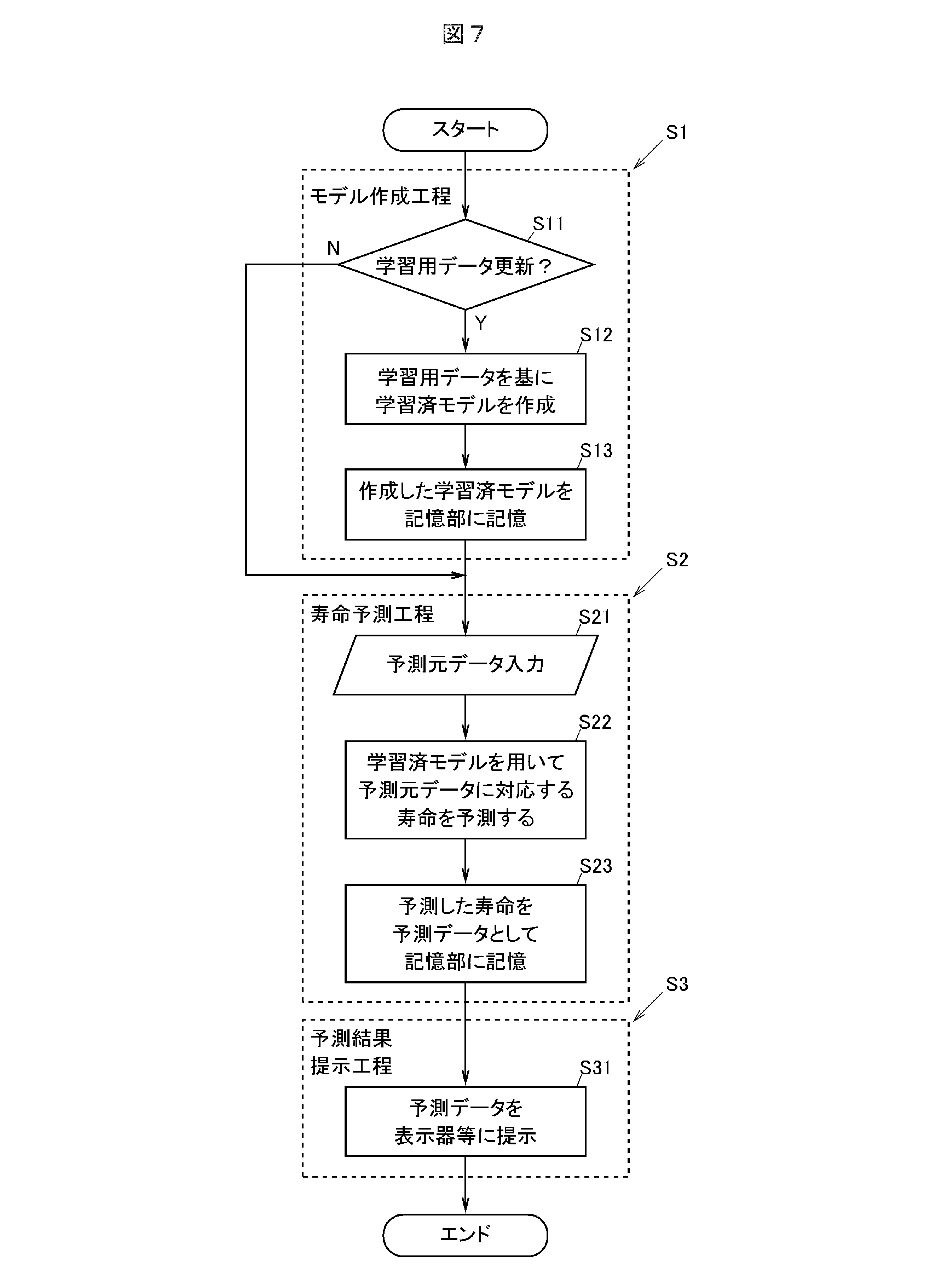
図7は、本実施の形態に係る窒化物半導体発光素子の寿命予測方法の制御フローを示すフロー図である。図7の制御フローは、寿命の予測を行う際に実行される。図7の制御フローに先立って、学習用データ取得部21による学習用データ31の取得、及び取得した学習用データ31の記憶部3への記憶の処理が随時行われる。
(Method for predicting lifetime of nitride semiconductor light emitting device)
Fig. 7 is a flow diagram showing a control flow of the lifetime prediction method for a nitride semiconductor light emitting device according to the present embodiment. The control flow of Fig. 7 is executed when predicting a lifetime. Prior to the control flow of Fig. 7, the learning
図7に示すように、本実施の形態に係る窒化物半導体発光素子の寿命予測方法では、ステップS1のモデル作成工程と、ステップS2の寿命予測工程と、ステップS3の予測結果提示工程と、が順次行われる。 As shown in FIG. 7, in the method for predicting the lifetime of a nitride semiconductor light-emitting element according to this embodiment, a model creation process in step S1, a lifetime prediction process in step S2, and a prediction result presentation process in step S3 are performed in sequence.
ステップS1のモデル作成工程では、まず、ステップS11にて、モデル作成部22が、前回学習済モデル32を作成したとき以降で学習用データ31が更新されたかを判定する。ステップS11の判定は、学習済モデル32の作成日時と、学習用データ31の更新日時とを比較することにより行うことができる。なお、ステップS11では、学習済モデル32が未作成の場合(初回時)には、学習用データ31が更新された(Yes)と判定する。ステップS11でNo(N)と判定された場合、ステップS2の寿命予測工程に進む。ステップS11でYes(Y)と判定された場合、ステップS12にて、モデル作成部22が、更新された学習用データ31を基に、予め設定された説明変数の各パラメータと目的変数である寿命との相関性を機械学習し、学習済モデル32を作成する。
In the model creation process of step S1, first, in step S11, the
本実施の形態では、ステップS11の機械学習において説明変数として用いるパラメータが、発光素子100を構成する層102~106の組成パラメータまたは物性パラメータの少なくとも一方を含んでいる。より好ましくは、下記のパラメータ
・各層102~106の欠陥密度
・n型半導体層103の膜抵抗
・p型半導体層106及び電子ブロック層105のドーピング濃度、及び膜厚
・p型半導体層106の成膜温度、成長速度
については、寿命への影響が非常に大きいため、一定とみなせない程度のバラつきがデータに生じている場合には、説明変数に含めることが望ましい。その上で、組成パラメータや物性パラメータを用いる層の成膜温度を製造パラメータとして用いるとよい。図4で説明したように、少なくとも、p型半導体層106の膜厚を説明変数として用いる場合には、p型半導体層106の成膜温度も説明変数に含めることが望ましい。そして、ウエハ上の位置を表す位置パラメータを説明変数に含めることがより望ましい。なお、図7では図示していないが、ステップS12の前に、どのパラメータを説明変数に用いるかを選択するステップを追加してもよい。
In this embodiment, the parameters used as explanatory variables in the machine learning of step S11 include at least one of the composition parameters or physical property parameters of the
ステップS12で学習済モデル32を作成した後、ステップS13にて、モデル作成部22が、作成した学習済モデル32を記憶部3に記憶し、ステップS2の寿命予測工程に進む。
After creating the trained
ステップS2の寿命予測工程では、まず、ステップS21にて、予測元データ33の入力を行う。この際、例えば、表示器4に予測元データ33の入力画面を表示して、入力装置5により予測元データ33を入力できるようにしてもよい。また、予測元データ33をファイル形式で入力する場合には、ファイルの入力を促す表示等を表示器4に表示してもよい。その後、ステップS22にて、寿命予測部23が、記憶部3に記憶された学習済モデル32を用いて、予測元データ33に対応する寿命を予測する。その後、ステップS23にて、寿命予測部23が、予測した寿命の値を、予測データ34として記憶部3に記憶し、ステップS3の予測結果提示工程に進む。なお、ウエハ上の位置を表す位置パラメータを説明変数に用いて学習済モデル32を作成している場合には、寿命予測工程にて、予測元データ33と、予め設定されたウエハ上の複数の位置のデータ(例えば、ウエハ中心部、外縁部など)とを用いて、設定されたウエハ上の複数の位置それぞれにおける寿命を求めてもよい。また、この場合、寿命予測工程では、例えばウエハ上の複数の位置での寿命の予測値の平均値や中央値を演算する等して、ウエハ全体での寿命評価のための指標値を演算してもよく、この指標値を予測データ34に含めてもよい。
In the life prediction process of step S2, first, in step S21, the
ステップS3の予測結果提示工程では、ステップS31にて、ステップS3の予測結果提示部24が、記憶部3に記憶された予測データ34を表示器4に提示することで、寿命の予測結果を提示する。その後、処理を終了する。
In the prediction result presentation process of step S3, in step S31, the prediction
本実施の形態では、寿命の予測時に学習済モデル32の更新を行う場合について説明したが、これに限らず、学習用データ31の更新状況を監視し、学習用データ31の更新の度に学習済モデル32を更新するようにモデル作成部22を構成してもよい。また、所定の期間毎(例えば毎週あるいは毎月)に学習済モデル32を更新するようにモデル作成部22を構成してもよい。
In this embodiment, a case has been described in which the trained
(実施の形態の作用及び効果)
以上説明した実施の形態によれば、以下のような作用及び効果が得られる。
(Functions and Effects of the Embodiments)
According to the embodiment described above, the following actions and effects can be obtained.
(1)発光素子100を構成する層の組成パラメータまたは物性パラメータの少なくとも一方と、組成パラメータまたは物性パラメータの値を調整する際に変更する製造条件パラメータと寿命との相関性を機械学習した学習済モデル32を用い、かつ、組成パラメータまたは物性パラメータを学習に用いる所定の層の成膜温度を製造条件パラメータとして学習に用いることで、発光素子100の寿命を精度よく予測することが可能になる。その結果、発光素子100を試作することなく寿命を予測することが可能になり、長い期間をかけて試作・評価を繰り返して試行錯誤することなく、短かい期間で開発を行うことが可能になる。
(1) By using a trained
(2)特に、組成パラメータとしてp型半導体層106の膜厚を用いる場合、製造条件パラメータとしてp型半導体層106の成膜温度をさらに学習に用いることで、寿命の予測精度が向上する。
(2) In particular, when the thickness of the p-
(3)さらに、ウエハ上の位置を表す位置パラメータを説明変数に用いることで、寿命の予測精度がより向上する。 (3) Furthermore, by using position parameters representing the position on the wafer as explanatory variables, the accuracy of lifetime prediction can be further improved.
(4)ウエハ上の位置を表す位置パラメータを説明変数に用いる場合、設定されたウエハ上の複数の位置それぞれにおける寿命を予測し、得られた予測値からウエハ全体での寿命評価のための指標値を演算することで、ウエハ上の位置による寿命のばらつきを考慮したウエハ全体の寿命評価を行うことが可能になる。 (4) When position parameters representing the position on the wafer are used as explanatory variables, the lifetime at each of multiple positions on the set wafer is predicted, and an index value for lifetime evaluation of the entire wafer is calculated from the predicted values, making it possible to evaluate the lifetime of the entire wafer while taking into account the variation in lifetime due to position on the wafer.
(実施の形態のまとめ)
次に、以上説明した実施の形態から把握される技術思想について、実施の形態における符号等を援用して記載する。
(Summary of the embodiment)
Next, the technical ideas grasped from the above-described embodiment will be described by using the reference numerals and the like in the embodiment.
[1]窒化物半導体発光素子(100)の寿命を予測する方法であって、少なくとも、前記窒化物半導体発光素子(100)を構成する層(102~106)の組成を規定するパラメータである組成パラメータ、または前記窒化物半導体発光素子(100)を構成する層(102~106)の物性を規定するパラメータである物性パラメータの少なくとも一方と、前記組成パラメータまたは前記物性パラメータの値を調整する際に変更する前記窒化物半導体発光素子(100)の製造条件である製造条件パラメータと、前記窒化物半導体発光素子(100)の寿命との相関性を学習して学習済モデル(32)を作成するモデル作成工程と、前記学習済モデル(32)を用いて寿命を予測する寿命予測工程と、を備え、前記モデル作成工程では、前記窒化物半導体発光素子(100)の所定の層の前記組成パラメータまたは前記物性パラメータの少なくとも一方を前記学習に用いると共に、前記所定の層の成膜温度を前記製造条件パラメータとして前記学習に用いる、窒化物半導体発光素子の寿命予測方法。 [1] A method for predicting the lifetime of a nitride semiconductor light-emitting device (100), comprising: a model creation step of learning a correlation between at least one of a composition parameter that is a parameter defining the composition of the layers (102-106) constituting the nitride semiconductor light-emitting device (100) or a physical property parameter that is a parameter defining the physical property of the layers (102-106) constituting the nitride semiconductor light-emitting device (100), a manufacturing condition parameter that is a manufacturing condition of the nitride semiconductor light-emitting device (100) that is changed when adjusting the value of the composition parameter or the physical property parameter, and the lifetime of the nitride semiconductor light-emitting device (100) to create a trained model (32); and a lifetime prediction step of predicting the lifetime using the trained model (32), in which in the model creation step, at least one of the composition parameter or the physical property parameter of a predetermined layer of the nitride semiconductor light-emitting device (100) is used in the learning, and the film formation temperature of the predetermined layer is used as the manufacturing condition parameter in the learning.
[2]前記所定の層が、AlGaNからなるp型半導体層(106)であり、少なくとも、前記物性パラメータである前記p型半導体層(106)の膜厚と、前記製造条件パラメータである前記p型半導体層(106)の成膜温度と、を前記学習に用いる、[1]に記載の窒化物半導体発光素子の寿命予測方法。 [2] The method for predicting the lifetime of a nitride semiconductor light-emitting element according to [1], in which the predetermined layer is a p-type semiconductor layer (106) made of AlGaN, and at least the film thickness of the p-type semiconductor layer (106), which is the physical property parameter, and the deposition temperature of the p-type semiconductor layer (106), which is the manufacturing condition parameter, are used in the learning.
[3]さらに、ウエハ上の位置を表す位置パラメータを、前記学習に用いる、[2]に記載の窒化物半導体発光素子の寿命予測方法。 [3] The method for predicting lifetime of a nitride semiconductor light-emitting element according to [2], further comprising using a position parameter representing a position on the wafer for the learning.
[4]前記寿命予測工程では、予め設定された前記ウエハ上の複数の位置のデータを用いて、設定された前記ウエハ上の複数の位置それぞれにおける寿命を予測し、前記ウエハ上の複数の位置での寿命の予測値を用いて、前記ウエハ全体での寿命評価のための指標値を演算する、[3]に記載の窒化物半導体発光素子の寿命予測方法。 [4] The lifetime prediction method for a nitride semiconductor light-emitting element described in [3], in which the lifetime prediction step predicts the lifetime at each of a plurality of preset positions on the wafer using data from the plurality of preset positions on the wafer, and calculates an index value for lifetime evaluation of the entire wafer using the predicted lifetime values at the plurality of positions on the wafer.
[5]窒化物半導体発光素子(100)の寿命を予測する装置であって、少なくとも、前記窒化物半導体発光素子(100)を構成する層(102~106)の組成を規定するパラメータである組成パラメータ、または前記窒化物半導体発光素子(100)を構成する層(102~106)の物性を規定するパラメータである物性パラメータの少なくとも一方と、前記組成パラメータまたは前記物性パラメータの値を調整する際に変更する前記窒化物半導体発光素子(100)の製造条件である製造条件パラメータと、前記窒化物半導体発光素子(100)の寿命との相関性を学習して学習済モデル(32)を作成するモデル作成部(22)と、前記学習済モデル(32)を用いて寿命を予測する寿命予測部(23)と、を備え、前記モデル作成部(22)は、前記窒化物半導体発光素子(100)の所定の層の前記組成パラメータまたは前記物性パラメータの少なくとも一方を前記学習に用いると共に、前記所定の層の成膜温度を前記製造条件パラメータとして前記学習に用いる、窒化物半導体発光素子の寿命予測装置(1)。 [5] An apparatus for predicting the lifetime of a nitride semiconductor light-emitting element (100), comprising at least one of a composition parameter that is a parameter defining the composition of the layers (102-106) constituting the nitride semiconductor light-emitting element (100) or a physical property parameter that is a parameter defining the physical property of the layers (102-106) constituting the nitride semiconductor light-emitting element (100), and a manufacturing condition parameter that is a manufacturing condition of the nitride semiconductor light-emitting element (100) that is changed when adjusting the value of the composition parameter or the physical property parameter. A lifetime prediction device (1) for a nitride semiconductor light-emitting element, comprising: a model creation unit (22) that learns the correlation with the lifetime of the nitride semiconductor light-emitting element (100) and creates a trained model (32); and a lifetime prediction unit (23) that predicts the lifetime using the trained model (32), wherein the model creation unit (22) uses at least one of the composition parameters or the physical property parameters of a specified layer of the nitride semiconductor light-emitting element (100) for the learning, and uses the film formation temperature of the specified layer as the manufacturing condition parameter for the learning.
(付記)
以上、本発明の実施の形態を説明したが、上記に記載した実施の形態は特許請求の範囲に係る発明を限定するものではない。また、実施の形態の中で説明した特徴の組合せの全てが発明の課題を解決するための手段に必須であるとは限らない点に留意すべきである。また、本発明は、その趣旨を逸脱しない範囲で適宜変形して実施することが可能である。
(Additional Note)
Although the embodiment of the present invention has been described above, the invention according to the claims is not limited to the embodiment described above. It should be noted that not all of the combinations of features described in the embodiment are essential to the means for solving the problems of the invention. The present invention can be modified appropriately without departing from the spirit of the invention.
1…窒化物半導体発光素子の寿命予測装置
2…制御部
21…学習用データ取得部
22…モデル作成部
23…寿命予測部
24…予測結果提示部
3…記憶部
31…学習用データ
32…学習済モデル
33…予測元データ
34…予測データ
100…窒化物半導体発光素子(発光素子)
101…基板
102…バッファ層
103…n型半導体層
104…活性層
104a…バリア層
104b…井戸層
105…電子ブロック層
106…p型半導体層
1...Nitride semiconductor light-emitting element
101...
Claims (5)
前記窒化物半導体発光素子は、バッファ層、n型半導体層、バリア層及び井戸層を有する活性層、電子ブロック層、及びp型半導体層を含み、
少なくとも、前記窒化物半導体発光素子を構成する層の組成を規定するパラメータである組成パラメータと、または前記窒化物半導体発光素子を構成する層の物性を規定するパラメータである物性パラメータと、前記組成パラメータまたは前記物性パラメータの値を調整する際に変更する前記窒化物半導体発光素子の製造条件である製造条件パラメータと、前記窒化物半導体発光素子の寿命との相関性を学習して学習済モデルを作成するモデル作成工程と、
前記学習済モデルを用いて寿命を予測する寿命予測工程と、を備え、
前記組成パラメータは、ドーピング濃度を含み、
前記物性パラメータは、欠陥密度、膜抵抗、膜厚を含み、
前記製造条件パラメータは、成膜温度、成膜時間、成長速度、及びTMA(トリメチルアルミニウム)、TMG(トリメチルガリウム)、TMSi(テトラメチルシラン)、Cp2Mg(ビスシクロペンタジエニルマグネシウム)、及びNH3の流量を含み、
前記モデル作成工程では、前記窒化物半導体発光素子の所定の層の前記組成パラメータまたは前記物性パラメータの少なくとも一方を前記学習に用いると共に、前記所定の層の成膜温度を前記製造条件パラメータとして前記学習に用い、
前記寿命予測工程では、前記学習済モデルに、予測対象の窒化物半導体発光素子の寿命以外の前記各パラメータを入力して寿命を予測し出力する、
窒化物半導体発光素子の寿命予測方法。 A method for predicting a lifetime of a nitride semiconductor light emitting device, comprising:
The nitride semiconductor light emitting device includes a buffer layer, an n-type semiconductor layer, an active layer having a barrier layer and a well layer, an electron blocking layer, and a p-type semiconductor layer,
a model creation step of learning a correlation between at least a composition parameter that is a parameter defining a composition of a layer constituting the nitride semiconductor light-emitting device, or a physical property parameter that is a parameter defining a physical property of a layer constituting the nitride semiconductor light-emitting device, a manufacturing condition parameter that is a manufacturing condition of the nitride semiconductor light-emitting device that is changed when adjusting the value of the composition parameter or the physical property parameter, and a lifetime of the nitride semiconductor light-emitting device to create a learned model;
A life prediction step of predicting a life using the trained model,
the compositional parameters include a doping concentration;
The physical parameters include a defect density, a film resistance, and a film thickness.
The manufacturing condition parameters include a film formation temperature, a film formation time, a growth rate, and flow rates of TMA (trimethylaluminum), TMG (trimethylgallium), TMSi ( tetramethylsilane ), Cp 2 Mg (biscyclopentadienylmagnesium), and NH 3 ;
In the model creation step, at least one of the composition parameters and the physical property parameters of a predetermined layer of the nitride semiconductor light emitting device is used in the learning, and a film formation temperature of the predetermined layer is used as the manufacturing condition parameter in the learning;
In the lifetime prediction step, the parameters other than the lifetime of the nitride semiconductor light emitting element to be predicted are input to the trained model, and the lifetime is predicted and output.
A method for predicting the lifetime of a nitride semiconductor light-emitting device.
少なくとも、前記物性パラメータである前記p型半導体層の膜厚と、前記製造条件パラメータである前記p型半導体層の成膜温度と、を前記学習に用いる、
請求項1に記載の窒化物半導体発光素子の寿命予測方法。 the predetermined layer is a p-type semiconductor layer made of AlGaN,
At least a thickness of the p-type semiconductor layer, which is the physical property parameter, and a deposition temperature of the p-type semiconductor layer, which is the manufacturing condition parameter, are used for the learning.
The method for predicting a lifetime of a nitride semiconductor light emitting device according to claim 1 .
請求項2に記載の窒化物半導体発光素子の寿命予測方法。 Furthermore, a position parameter representing a position on the wafer is used for the learning.
The method for predicting a lifetime of a nitride semiconductor light-emitting device according to claim 2 .
予め設定された前記ウエハ上の複数の位置のデータを用いて、設定された前記ウエハ上の複数の位置それぞれにおける寿命を予測し、
前記ウエハ上の複数の位置での寿命の予測値を用いて、前記ウエハ全体での寿命評価のための指標値を演算する、
請求項3に記載の窒化物半導体発光素子の寿命予測方法。 In the life prediction step,
predicting a lifetime at each of a plurality of preset positions on the wafer using data on the plurality of preset positions on the wafer;
calculating an index value for evaluating a lifetime over the entire wafer using predicted lifetime values at a plurality of positions on the wafer;
The method for predicting a lifetime of a nitride semiconductor light-emitting device according to claim 3 .
前記窒化物半導体発光素子は、バッファ層、n型半導体層、バリア層及び井戸層を有する活性層、電子ブロック層、及びp型半導体層を含み、
少なくとも、前記窒化物半導体発光素子を構成する層の組成を規定するパラメータである組成パラメータと、前記窒化物半導体発光素子を構成する層の物性を規定するパラメータである物性パラメータと、前記組成パラメータまたは前記物性パラメータの値を調整する際に変更する前記窒化物半導体発光素子の製造条件である製造条件パラメータと、前記窒化物半導体発光素子の寿命との相関性を学習して学習済モデルを作成するモデル作成部と、
前記学習済モデルを用いて寿命を予測する寿命予測部と、を備え、
前記組成パラメータは、ドーピング濃度を含み、
前記物性パラメータは、欠陥密度、膜抵抗、膜厚を含み、
前記製造条件パラメータは、成膜温度、成膜時間、成長速度、及びTMA(トリメチルアルミニウム)、TMG(トリメチルガリウム)、TMSi(テトラメチルシラン)、Cp 2 Mg(ビスシクロペンタジエニルマグネシウム)、及びNH 3 の流量を含み、
前記モデル作成部は、前記窒化物半導体発光素子の所定の層の前記組成パラメータまたは前記物性パラメータの少なくとも一方を前記学習に用いると共に、前記所定の層の成膜温度を前記製造条件パラメータとして前記学習に用い、
前記寿命予測部は、前記学習済モデルに、予測対象の窒化物半導体発光素子の寿命以外の前記各パラメータを入力して寿命を予測し出力する、
窒化物半導体発光素子の寿命予測装置。 An apparatus for predicting a lifetime of a nitride semiconductor light emitting device, comprising:
The nitride semiconductor light emitting device includes a buffer layer, an n-type semiconductor layer, an active layer having a barrier layer and a well layer, an electron blocking layer, and a p-type semiconductor layer,
a model creation unit that learns correlations between at least composition parameters that are parameters defining compositions of layers that constitute the nitride semiconductor light-emitting device , physical property parameters that are parameters defining physical properties of layers that constitute the nitride semiconductor light-emitting device , manufacturing condition parameters that are manufacturing conditions of the nitride semiconductor light-emitting device that are changed when adjusting the values of the composition parameters or the physical property parameters, and a lifetime of the nitride semiconductor light-emitting device to create a trained model;
A life prediction unit that predicts a life using the trained model,
the compositional parameters include a doping concentration;
The physical parameters include a defect density, a film resistance, and a film thickness.
The manufacturing condition parameters include a film formation temperature, a film formation time, a growth rate, and flow rates of TMA (trimethylaluminum), TMG (trimethylgallium), TMSi (tetramethylsilane), Cp 2 Mg (biscyclopentadienylmagnesium), and NH 3 ;
the model creation unit uses at least one of the composition parameters or the physical property parameters of a predetermined layer of the nitride semiconductor light emitting device for the learning, and also uses a film formation temperature of the predetermined layer as the manufacturing condition parameter for the learning ;
The lifetime prediction unit inputs each parameter other than the lifetime of the nitride semiconductor light emitting element to be predicted into the learned model, predicts and outputs the lifetime.
A lifetime prediction device for nitride semiconductor light-emitting elements.
Priority Applications (3)
| Application Number | Priority Date | Filing Date | Title |
|---|---|---|---|
| JP2024076243A JP7626894B2 (en) | 2023-05-09 | 2024-05-09 | Lifetime prediction device for semiconductor light emitting devices |
| US18/659,573 US20240378341A1 (en) | 2023-05-09 | 2024-05-09 | Method and device for predicting lifetime of nitride semiconductor light-emitting element |
| JP2024203384A JP2025019190A (en) | 2023-05-09 | 2024-11-21 | Semiconductor light emitting device manufacturing system |
Applications Claiming Priority (2)
| Application Number | Priority Date | Filing Date | Title |
|---|---|---|---|
| JP2023077203 | 2023-05-09 | ||
| JP2023077203 | 2023-05-09 |
Related Child Applications (1)
| Application Number | Title | Priority Date | Filing Date |
|---|---|---|---|
| JP2024076243A Division JP7626894B2 (en) | 2023-05-09 | 2024-05-09 | Lifetime prediction device for semiconductor light emitting devices |
Publications (2)
| Publication Number | Publication Date |
|---|---|
| JP7511734B1 true JP7511734B1 (en) | 2024-07-05 |
| JP2024162968A JP2024162968A (en) | 2024-11-21 |
Family
ID=91714582
Family Applications (3)
| Application Number | Title | Priority Date | Filing Date |
|---|---|---|---|
| JP2023183043A Active JP7511734B1 (en) | 2023-05-09 | 2023-10-25 | Method and apparatus for predicting lifetime of nitride semiconductor light emitting device |
| JP2024076243A Active JP7626894B2 (en) | 2023-05-09 | 2024-05-09 | Lifetime prediction device for semiconductor light emitting devices |
| JP2024203384A Pending JP2025019190A (en) | 2023-05-09 | 2024-11-21 | Semiconductor light emitting device manufacturing system |
Family Applications After (2)
| Application Number | Title | Priority Date | Filing Date |
|---|---|---|---|
| JP2024076243A Active JP7626894B2 (en) | 2023-05-09 | 2024-05-09 | Lifetime prediction device for semiconductor light emitting devices |
| JP2024203384A Pending JP2025019190A (en) | 2023-05-09 | 2024-11-21 | Semiconductor light emitting device manufacturing system |
Country Status (2)
| Country | Link |
|---|---|
| US (1) | US20240378341A1 (en) |
| JP (3) | JP7511734B1 (en) |
Citations (4)
| Publication number | Priority date | Publication date | Assignee | Title |
|---|---|---|---|---|
| JP2002043695A (en) | 2000-07-26 | 2002-02-08 | Sharp Corp | Light emitting element |
| JP2002246698A (en) | 2001-02-15 | 2002-08-30 | Sharp Corp | Nitride semiconductor light emitting device and manufacturing method thereof |
| WO2006059389A1 (en) | 2004-12-03 | 2006-06-08 | Mitsubishi Denki Kabushiki Kaisha | Light wavelength conversion light source |
| JP2018112410A (en) | 2017-01-06 | 2018-07-19 | 株式会社東芝 | Electronic component life prediction apparatus and electronic component life prediction method |
Family Cites Families (7)
| Publication number | Priority date | Publication date | Assignee | Title |
|---|---|---|---|---|
| JP2003229645A (en) | 2002-01-31 | 2003-08-15 | Nec Corp | Quantum well structure, semiconductor device using the same, and method of manufacturing semiconductor device |
| GB0307406D0 (en) | 2003-03-31 | 2003-05-07 | British Telecomm | Data analysis system and method |
| JP2004335712A (en) | 2003-05-07 | 2004-11-25 | Sharp Corp | Oxide semiconductor light emitting device and processing method thereof |
| JP4916459B2 (en) | 2003-06-05 | 2012-04-11 | パナソニック株式会社 | Manufacturing method of semiconductor light emitting device |
| JP6360090B2 (en) * | 2016-03-10 | 2018-07-18 | ファナック株式会社 | Machine learning device, laser device, and machine learning method |
| JP7182059B2 (en) | 2018-01-17 | 2022-12-02 | 横河電機株式会社 | Measurement value prediction module, measurement value prediction program, and measurement value prediction method |
| JP7577666B2 (en) * | 2019-08-29 | 2024-11-05 | 株式会社半導体エネルギー研究所 | Property Prediction System |
-
2023
- 2023-10-25 JP JP2023183043A patent/JP7511734B1/en active Active
-
2024
- 2024-05-09 US US18/659,573 patent/US20240378341A1/en active Pending
- 2024-05-09 JP JP2024076243A patent/JP7626894B2/en active Active
- 2024-11-21 JP JP2024203384A patent/JP2025019190A/en active Pending
Patent Citations (4)
| Publication number | Priority date | Publication date | Assignee | Title |
|---|---|---|---|---|
| JP2002043695A (en) | 2000-07-26 | 2002-02-08 | Sharp Corp | Light emitting element |
| JP2002246698A (en) | 2001-02-15 | 2002-08-30 | Sharp Corp | Nitride semiconductor light emitting device and manufacturing method thereof |
| WO2006059389A1 (en) | 2004-12-03 | 2006-06-08 | Mitsubishi Denki Kabushiki Kaisha | Light wavelength conversion light source |
| JP2018112410A (en) | 2017-01-06 | 2018-07-19 | 株式会社東芝 | Electronic component life prediction apparatus and electronic component life prediction method |
Also Published As
| Publication number | Publication date |
|---|---|
| JP2024163074A (en) | 2024-11-21 |
| JP2024162968A (en) | 2024-11-21 |
| JP7626894B2 (en) | 2025-02-04 |
| US20240378341A1 (en) | 2024-11-14 |
| JP2025019190A (en) | 2025-02-06 |
Similar Documents
| Publication | Publication Date | Title |
|---|---|---|
| KR101804493B1 (en) | Optoelectronic device with modulation doping | |
| JP5175918B2 (en) | Semiconductor light emitting device | |
| US9385271B2 (en) | Device with transparent and higher conductive regions in lateral cross section of semiconductor layer | |
| US9042420B2 (en) | Device with transparent and higher conductive regions in lateral cross section of semiconductor layer | |
| US20160118531A1 (en) | Optoelectronic Device with Modulation Doping | |
| JP6641335B2 (en) | Nitride semiconductor light emitting device and method of manufacturing nitride semiconductor light emitting device | |
| JP6686172B2 (en) | Nitride semiconductor light emitting device | |
| JP7355740B2 (en) | light emitting element | |
| JP7511734B1 (en) | Method and apparatus for predicting lifetime of nitride semiconductor light emitting device | |
| JP7488410B1 (en) | Method and device for predicting light output of nitride semiconductor light emitting device | |
| CN101267009A (en) | Manufacturing method of semiconductor optical element | |
| Ajia et al. | Subquantum-well influence on carrier dynamics in high efficiency DUV dislocation-free AlGaN/AlGaN-based multiple quantum wells | |
| JP5349420B2 (en) | Manufacturing method of semiconductor light emitting device | |
| TWI269463B (en) | Method for manufacturing high brightness light-emitting diode | |
| JP6917953B2 (en) | Nitride semiconductor light emitting device | |
| JP5889981B2 (en) | Semiconductor light emitting device | |
| TWI757598B (en) | deep ultraviolet light emitting element | |
| JP2021192457A (en) | Nitride semiconductor light emitting device and method for manufacturing nitride semiconductor light emitting device | |
| JP6091366B2 (en) | Operation management method for vapor phase growth apparatus, and method for producing laminate using the method | |
| Muhin et al. | Analysis of the External Quantum Efficiency of 233 nm Far‐Ultraviolet‐C‐Light Emitting Diodes with Distributed Polarization Doped p‐AlGaN‐Layers | |
| KR100586975B1 (en) | Nitride semiconductor device and manufacturing method | |
| JP5606595B2 (en) | Manufacturing method of semiconductor light emitting device | |
| Höpfner et al. | Origin of the efficiency drop in far-UVC LEDs emitting between 218 and 238 nm | |
| Kioupakis et al. | Energy Conversion: Solid‐State Lighting | |
| JP5615334B2 (en) | Semiconductor light emitting device |
Legal Events
| Date | Code | Title | Description |
|---|---|---|---|
| A621 | Written request for application examination |
Free format text: JAPANESE INTERMEDIATE CODE: A621 Effective date: 20231025 |
|
| A871 | Explanation of circumstances concerning accelerated examination |
Free format text: JAPANESE INTERMEDIATE CODE: A871 Effective date: 20231025 |
|
| A131 | Notification of reasons for refusal |
Free format text: JAPANESE INTERMEDIATE CODE: A131 Effective date: 20231121 |
|
| A521 | Request for written amendment filed |
Free format text: JAPANESE INTERMEDIATE CODE: A523 Effective date: 20231228 |
|
| A02 | Decision of refusal |
Free format text: JAPANESE INTERMEDIATE CODE: A02 Effective date: 20240220 |
|
| A521 | Request for written amendment filed |
Free format text: JAPANESE INTERMEDIATE CODE: A523 Effective date: 20240509 |
|
| A911 | Transfer to examiner for re-examination before appeal (zenchi) |
Free format text: JAPANESE INTERMEDIATE CODE: A911 Effective date: 20240516 |
|
| TRDD | Decision of grant or rejection written | ||
| A01 | Written decision to grant a patent or to grant a registration (utility model) |
Free format text: JAPANESE INTERMEDIATE CODE: A01 Effective date: 20240618 |
|
| A61 | First payment of annual fees (during grant procedure) |
Free format text: JAPANESE INTERMEDIATE CODE: A61 Effective date: 20240625 |
|
| R150 | Certificate of patent or registration of utility model |
Ref document number: 7511734 Country of ref document: JP Free format text: JAPANESE INTERMEDIATE CODE: R150 |