JP7493576B2 - トランジスタ - Google Patents
トランジスタ Download PDFInfo
- Publication number
- JP7493576B2 JP7493576B2 JP2022194011A JP2022194011A JP7493576B2 JP 7493576 B2 JP7493576 B2 JP 7493576B2 JP 2022194011 A JP2022194011 A JP 2022194011A JP 2022194011 A JP2022194011 A JP 2022194011A JP 7493576 B2 JP7493576 B2 JP 7493576B2
- Authority
- JP
- Japan
- Prior art keywords
- oxide
- conductor
- insulator
- transistor
- film
- Prior art date
- Legal status (The legal status is an assumption and is not a legal conclusion. Google has not performed a legal analysis and makes no representation as to the accuracy of the status listed.)
- Active
Links
- 239000004065 semiconductor Substances 0.000 claims description 354
- IJGRMHOSHXDMSA-UHFFFAOYSA-N Atomic nitrogen Chemical compound N#N IJGRMHOSHXDMSA-UHFFFAOYSA-N 0.000 claims description 193
- QVGXLLKOCUKJST-UHFFFAOYSA-N atomic oxygen Chemical compound [O] QVGXLLKOCUKJST-UHFFFAOYSA-N 0.000 claims description 173
- 239000001301 oxygen Substances 0.000 claims description 173
- 229910052760 oxygen Inorganic materials 0.000 claims description 173
- 229910052739 hydrogen Inorganic materials 0.000 claims description 119
- 239000001257 hydrogen Substances 0.000 claims description 115
- UFHFLCQGNIYNRP-UHFFFAOYSA-N Hydrogen Chemical compound [H][H] UFHFLCQGNIYNRP-UHFFFAOYSA-N 0.000 claims description 107
- 229910052757 nitrogen Inorganic materials 0.000 claims description 104
- 239000000463 material Substances 0.000 claims description 63
- 229910052751 metal Inorganic materials 0.000 claims description 52
- 239000002184 metal Substances 0.000 claims description 47
- 230000015572 biosynthetic process Effects 0.000 claims description 43
- 229910052782 aluminium Inorganic materials 0.000 claims description 32
- XAGFODPZIPBFFR-UHFFFAOYSA-N aluminium Chemical group [Al] XAGFODPZIPBFFR-UHFFFAOYSA-N 0.000 claims description 32
- 229910052738 indium Inorganic materials 0.000 claims description 27
- APFVFJFRJDLVQX-UHFFFAOYSA-N indium atom Chemical compound [In] APFVFJFRJDLVQX-UHFFFAOYSA-N 0.000 claims description 27
- 229910052684 Cerium Inorganic materials 0.000 claims description 16
- GWXLDORMOJMVQZ-UHFFFAOYSA-N cerium Chemical compound [Ce] GWXLDORMOJMVQZ-UHFFFAOYSA-N 0.000 claims description 16
- GYHNNYVSQQEPJS-UHFFFAOYSA-N Gallium Chemical compound [Ga] GYHNNYVSQQEPJS-UHFFFAOYSA-N 0.000 claims description 13
- 229910052733 gallium Inorganic materials 0.000 claims description 13
- 230000001186 cumulative effect Effects 0.000 claims description 11
- 229910052727 yttrium Inorganic materials 0.000 claims description 11
- VWQVUPCCIRVNHF-UHFFFAOYSA-N yttrium atom Chemical compound [Y] VWQVUPCCIRVNHF-UHFFFAOYSA-N 0.000 claims description 11
- ATJFFYVFTNAWJD-UHFFFAOYSA-N Tin Chemical compound [Sn] ATJFFYVFTNAWJD-UHFFFAOYSA-N 0.000 claims description 10
- 230000008859 change Effects 0.000 claims description 10
- 229910052718 tin Inorganic materials 0.000 claims description 10
- JBQYATWDVHIOAR-UHFFFAOYSA-N tellanylidenegermanium Chemical compound [Te]=[Ge] JBQYATWDVHIOAR-UHFFFAOYSA-N 0.000 claims description 8
- 239000004020 conductor Substances 0.000 description 334
- 239000012212 insulator Substances 0.000 description 309
- 239000010408 film Substances 0.000 description 295
- 238000000034 method Methods 0.000 description 171
- 230000006870 function Effects 0.000 description 89
- 230000015654 memory Effects 0.000 description 79
- 210000004027 cell Anatomy 0.000 description 65
- 125000004429 atom Chemical group 0.000 description 64
- 229910044991 metal oxide Inorganic materials 0.000 description 55
- 150000004706 metal oxides Chemical class 0.000 description 55
- 238000004544 sputter deposition Methods 0.000 description 55
- 230000008569 process Effects 0.000 description 48
- 239000010410 layer Substances 0.000 description 47
- 238000000231 atomic layer deposition Methods 0.000 description 45
- 239000012535 impurity Substances 0.000 description 45
- 238000012545 processing Methods 0.000 description 45
- 238000005229 chemical vapour deposition Methods 0.000 description 44
- 238000010438 heat treatment Methods 0.000 description 41
- 230000004888 barrier function Effects 0.000 description 37
- 239000007789 gas Substances 0.000 description 33
- 238000004519 manufacturing process Methods 0.000 description 33
- XLYOFNOQVPJJNP-UHFFFAOYSA-N water Substances O XLYOFNOQVPJJNP-UHFFFAOYSA-N 0.000 description 30
- 229910001868 water Inorganic materials 0.000 description 30
- 239000013078 crystal Substances 0.000 description 28
- TWNQGVIAIRXVLR-UHFFFAOYSA-N oxo(oxoalumanyloxy)alumane Chemical compound O=[Al]O[Al]=O TWNQGVIAIRXVLR-UHFFFAOYSA-N 0.000 description 27
- 239000000758 substrate Substances 0.000 description 26
- 229910052721 tungsten Inorganic materials 0.000 description 26
- 239000010937 tungsten Substances 0.000 description 26
- 239000012298 atmosphere Substances 0.000 description 24
- 238000004549 pulsed laser deposition Methods 0.000 description 23
- 238000009792 diffusion process Methods 0.000 description 22
- 238000001451 molecular beam epitaxy Methods 0.000 description 22
- WFKWXMTUELFFGS-UHFFFAOYSA-N tungsten Chemical compound [W] WFKWXMTUELFFGS-UHFFFAOYSA-N 0.000 description 22
- 239000011701 zinc Substances 0.000 description 22
- RYGMFSIKBFXOCR-UHFFFAOYSA-N Copper Chemical group [Cu] RYGMFSIKBFXOCR-UHFFFAOYSA-N 0.000 description 20
- 238000004364 calculation method Methods 0.000 description 18
- 230000000875 corresponding effect Effects 0.000 description 18
- 238000010894 electron beam technology Methods 0.000 description 18
- 125000004430 oxygen atom Chemical group O* 0.000 description 18
- 229910052802 copper Inorganic materials 0.000 description 17
- 239000010949 copper Substances 0.000 description 17
- 239000010409 thin film Substances 0.000 description 17
- XKRFYHLGVUSROY-UHFFFAOYSA-N Argon Chemical compound [Ar] XKRFYHLGVUSROY-UHFFFAOYSA-N 0.000 description 16
- 238000010586 diagram Methods 0.000 description 16
- 238000001312 dry etching Methods 0.000 description 16
- 238000003860 storage Methods 0.000 description 16
- 238000003917 TEM image Methods 0.000 description 15
- 238000005259 measurement Methods 0.000 description 15
- 239000000969 carrier Substances 0.000 description 14
- 238000006243 chemical reaction Methods 0.000 description 14
- 125000004433 nitrogen atom Chemical group N* 0.000 description 14
- 229910052581 Si3N4 Inorganic materials 0.000 description 13
- RTAQQCXQSZGOHL-UHFFFAOYSA-N Titanium Chemical compound [Ti] RTAQQCXQSZGOHL-UHFFFAOYSA-N 0.000 description 13
- NRTOMJZYCJJWKI-UHFFFAOYSA-N Titanium nitride Chemical compound [Ti]#N NRTOMJZYCJJWKI-UHFFFAOYSA-N 0.000 description 13
- VYPSYNLAJGMNEJ-UHFFFAOYSA-N silicon dioxide Inorganic materials O=[Si]=O VYPSYNLAJGMNEJ-UHFFFAOYSA-N 0.000 description 13
- HQVNEWCFYHHQES-UHFFFAOYSA-N silicon nitride Chemical compound N12[Si]34N5[Si]62N3[Si]51N64 HQVNEWCFYHHQES-UHFFFAOYSA-N 0.000 description 13
- 229910052719 titanium Inorganic materials 0.000 description 13
- 239000010936 titanium Substances 0.000 description 13
- 230000005355 Hall effect Effects 0.000 description 12
- -1 element M Chemical compound 0.000 description 12
- 230000003647 oxidation Effects 0.000 description 12
- 238000007254 oxidation reaction Methods 0.000 description 12
- 238000009832 plasma treatment Methods 0.000 description 12
- MZLGASXMSKOWSE-UHFFFAOYSA-N tantalum nitride Chemical compound [Ta]#N MZLGASXMSKOWSE-UHFFFAOYSA-N 0.000 description 12
- 230000007547 defect Effects 0.000 description 11
- 238000005530 etching Methods 0.000 description 11
- 238000011282 treatment Methods 0.000 description 11
- 238000001039 wet etching Methods 0.000 description 11
- ZOKXTWBITQBERF-UHFFFAOYSA-N Molybdenum Chemical compound [Mo] ZOKXTWBITQBERF-UHFFFAOYSA-N 0.000 description 10
- XUIMIQQOPSSXEZ-UHFFFAOYSA-N Silicon Chemical compound [Si] XUIMIQQOPSSXEZ-UHFFFAOYSA-N 0.000 description 10
- 239000003990 capacitor Substances 0.000 description 10
- 229910052750 molybdenum Inorganic materials 0.000 description 10
- 239000011733 molybdenum Substances 0.000 description 10
- 229910052710 silicon Inorganic materials 0.000 description 10
- 239000010703 silicon Substances 0.000 description 10
- 229910052814 silicon oxide Inorganic materials 0.000 description 10
- MYMOFIZGZYHOMD-UHFFFAOYSA-N Dioxygen Chemical compound O=O MYMOFIZGZYHOMD-UHFFFAOYSA-N 0.000 description 9
- 229910001882 dioxygen Inorganic materials 0.000 description 9
- 229910052735 hafnium Inorganic materials 0.000 description 9
- 239000011229 interlayer Substances 0.000 description 9
- 229910052786 argon Inorganic materials 0.000 description 8
- 238000004140 cleaning Methods 0.000 description 8
- 229910000449 hafnium oxide Inorganic materials 0.000 description 8
- WIHZLLGSGQNAGK-UHFFFAOYSA-N hafnium(4+);oxygen(2-) Chemical compound [O-2].[O-2].[Hf+4] WIHZLLGSGQNAGK-UHFFFAOYSA-N 0.000 description 8
- 239000002356 single layer Substances 0.000 description 8
- 238000004380 ashing Methods 0.000 description 7
- 229910001873 dinitrogen Inorganic materials 0.000 description 7
- VBJZVLUMGGDVMO-UHFFFAOYSA-N hafnium atom Chemical compound [Hf] VBJZVLUMGGDVMO-UHFFFAOYSA-N 0.000 description 7
- 150000002431 hydrogen Chemical class 0.000 description 7
- 125000004435 hydrogen atom Chemical group [H]* 0.000 description 7
- 150000002500 ions Chemical class 0.000 description 7
- PXHVJJICTQNCMI-UHFFFAOYSA-N Nickel Chemical compound [Ni] PXHVJJICTQNCMI-UHFFFAOYSA-N 0.000 description 6
- HCHKCACWOHOZIP-UHFFFAOYSA-N Zinc Chemical compound [Zn] HCHKCACWOHOZIP-UHFFFAOYSA-N 0.000 description 6
- XLOMVQKBTHCTTD-UHFFFAOYSA-N Zinc monoxide Chemical compound [Zn]=O XLOMVQKBTHCTTD-UHFFFAOYSA-N 0.000 description 6
- 238000012937 correction Methods 0.000 description 6
- 238000013461 design Methods 0.000 description 6
- 239000000203 mixture Substances 0.000 description 6
- 239000002159 nanocrystal Substances 0.000 description 6
- 230000002093 peripheral effect Effects 0.000 description 6
- 229910052715 tantalum Inorganic materials 0.000 description 6
- GUVRBAGPIYLISA-UHFFFAOYSA-N tantalum atom Chemical compound [Ta] GUVRBAGPIYLISA-UHFFFAOYSA-N 0.000 description 6
- 229910052725 zinc Inorganic materials 0.000 description 6
- 229910052779 Neodymium Inorganic materials 0.000 description 5
- 230000005684 electric field Effects 0.000 description 5
- 238000005516 engineering process Methods 0.000 description 5
- 238000001459 lithography Methods 0.000 description 5
- QEFYFXOXNSNQGX-UHFFFAOYSA-N neodymium atom Chemical compound [Nd] QEFYFXOXNSNQGX-UHFFFAOYSA-N 0.000 description 5
- RVTZCBVAJQQJTK-UHFFFAOYSA-N oxygen(2-);zirconium(4+) Chemical compound [O-2].[O-2].[Zr+4] RVTZCBVAJQQJTK-UHFFFAOYSA-N 0.000 description 5
- 238000002230 thermal chemical vapour deposition Methods 0.000 description 5
- 229910001928 zirconium oxide Inorganic materials 0.000 description 5
- XEEYBQQBJWHFJM-UHFFFAOYSA-N Iron Chemical compound [Fe] XEEYBQQBJWHFJM-UHFFFAOYSA-N 0.000 description 4
- 238000004833 X-ray photoelectron spectroscopy Methods 0.000 description 4
- 229910052783 alkali metal Inorganic materials 0.000 description 4
- 150000001340 alkali metals Chemical class 0.000 description 4
- 229910052784 alkaline earth metal Inorganic materials 0.000 description 4
- 150000001342 alkaline earth metals Chemical class 0.000 description 4
- 238000000576 coating method Methods 0.000 description 4
- AJNVQOSZGJRYEI-UHFFFAOYSA-N digallium;oxygen(2-) Chemical compound [O-2].[O-2].[O-2].[Ga+3].[Ga+3] AJNVQOSZGJRYEI-UHFFFAOYSA-N 0.000 description 4
- 230000000694 effects Effects 0.000 description 4
- 229910001195 gallium oxide Inorganic materials 0.000 description 4
- 239000011810 insulating material Substances 0.000 description 4
- MRELNEQAGSRDBK-UHFFFAOYSA-N lanthanum(3+);oxygen(2-) Chemical compound [O-2].[O-2].[O-2].[La+3].[La+3] MRELNEQAGSRDBK-UHFFFAOYSA-N 0.000 description 4
- 229910052451 lead zirconate titanate Inorganic materials 0.000 description 4
- 239000007769 metal material Substances 0.000 description 4
- 150000002739 metals Chemical class 0.000 description 4
- PLDDOISOJJCEMH-UHFFFAOYSA-N neodymium(3+);oxygen(2-) Chemical compound [O-2].[O-2].[O-2].[Nd+3].[Nd+3] PLDDOISOJJCEMH-UHFFFAOYSA-N 0.000 description 4
- QJGQUHMNIGDVPM-UHFFFAOYSA-N nitrogen group Chemical group [N] QJGQUHMNIGDVPM-UHFFFAOYSA-N 0.000 description 4
- 230000001590 oxidative effect Effects 0.000 description 4
- BPUBBGLMJRNUCC-UHFFFAOYSA-N oxygen(2-);tantalum(5+) Chemical compound [O-2].[O-2].[O-2].[O-2].[O-2].[Ta+5].[Ta+5] BPUBBGLMJRNUCC-UHFFFAOYSA-N 0.000 description 4
- 239000012466 permeate Substances 0.000 description 4
- 239000011347 resin Substances 0.000 description 4
- 229920005989 resin Polymers 0.000 description 4
- 238000000926 separation method Methods 0.000 description 4
- 229910001936 tantalum oxide Inorganic materials 0.000 description 4
- 229910052692 Dysprosium Inorganic materials 0.000 description 3
- 238000004435 EPR spectroscopy Methods 0.000 description 3
- MUBZPKHOEPUJKR-UHFFFAOYSA-N Oxalic acid Chemical compound OC(=O)C(O)=O MUBZPKHOEPUJKR-UHFFFAOYSA-N 0.000 description 3
- 229910052777 Praseodymium Inorganic materials 0.000 description 3
- 229910052771 Terbium Inorganic materials 0.000 description 3
- QCWXUUIWCKQGHC-UHFFFAOYSA-N Zirconium Chemical compound [Zr] QCWXUUIWCKQGHC-UHFFFAOYSA-N 0.000 description 3
- GPBUGPUPKAGMDK-UHFFFAOYSA-N azanylidynemolybdenum Chemical compound [Mo]#N GPBUGPUPKAGMDK-UHFFFAOYSA-N 0.000 description 3
- 230000005540 biological transmission Effects 0.000 description 3
- 230000003247 decreasing effect Effects 0.000 description 3
- 238000000151 deposition Methods 0.000 description 3
- 230000008021 deposition Effects 0.000 description 3
- KBQHZAAAGSGFKK-UHFFFAOYSA-N dysprosium atom Chemical compound [Dy] KBQHZAAAGSGFKK-UHFFFAOYSA-N 0.000 description 3
- YBMRDBCBODYGJE-UHFFFAOYSA-N germanium oxide Inorganic materials O=[Ge]=O YBMRDBCBODYGJE-UHFFFAOYSA-N 0.000 description 3
- 239000011261 inert gas Substances 0.000 description 3
- 230000004048 modification Effects 0.000 description 3
- 238000012986 modification Methods 0.000 description 3
- 229910052759 nickel Inorganic materials 0.000 description 3
- SIWVEOZUMHYXCS-UHFFFAOYSA-N oxo(oxoyttriooxy)yttrium Chemical compound O=[Y]O[Y]=O SIWVEOZUMHYXCS-UHFFFAOYSA-N 0.000 description 3
- PVADDRMAFCOOPC-UHFFFAOYSA-N oxogermanium Chemical compound [Ge]=O PVADDRMAFCOOPC-UHFFFAOYSA-N 0.000 description 3
- 230000003071 parasitic effect Effects 0.000 description 3
- 230000000737 periodic effect Effects 0.000 description 3
- PUDIUYLPXJFUGB-UHFFFAOYSA-N praseodymium atom Chemical compound [Pr] PUDIUYLPXJFUGB-UHFFFAOYSA-N 0.000 description 3
- 239000010453 quartz Substances 0.000 description 3
- 238000011160 research Methods 0.000 description 3
- GZCRRIHWUXGPOV-UHFFFAOYSA-N terbium atom Chemical compound [Tb] GZCRRIHWUXGPOV-UHFFFAOYSA-N 0.000 description 3
- OGIDPMRJRNCKJF-UHFFFAOYSA-N titanium oxide Inorganic materials [Ti]=O OGIDPMRJRNCKJF-UHFFFAOYSA-N 0.000 description 3
- 239000011787 zinc oxide Substances 0.000 description 3
- 229910052726 zirconium Inorganic materials 0.000 description 3
- 210000002925 A-like Anatomy 0.000 description 2
- ZOXJGFHDIHLPTG-UHFFFAOYSA-N Boron Chemical compound [B] ZOXJGFHDIHLPTG-UHFFFAOYSA-N 0.000 description 2
- OKTJSMMVPCPJKN-UHFFFAOYSA-N Carbon Chemical compound [C] OKTJSMMVPCPJKN-UHFFFAOYSA-N 0.000 description 2
- 208000005156 Dehydration Diseases 0.000 description 2
- KRHYYFGTRYWZRS-UHFFFAOYSA-N Fluorane Chemical compound F KRHYYFGTRYWZRS-UHFFFAOYSA-N 0.000 description 2
- FYYHWMGAXLPEAU-UHFFFAOYSA-N Magnesium Chemical compound [Mg] FYYHWMGAXLPEAU-UHFFFAOYSA-N 0.000 description 2
- NBIIXXVUZAFLBC-UHFFFAOYSA-N Phosphoric acid Chemical compound OP(O)(O)=O NBIIXXVUZAFLBC-UHFFFAOYSA-N 0.000 description 2
- 229910001080 W alloy Inorganic materials 0.000 description 2
- 239000000956 alloy Substances 0.000 description 2
- 238000013528 artificial neural network Methods 0.000 description 2
- 229910052788 barium Inorganic materials 0.000 description 2
- 230000008901 benefit Effects 0.000 description 2
- 229910052796 boron Inorganic materials 0.000 description 2
- 229910052799 carbon Inorganic materials 0.000 description 2
- 239000011248 coating agent Substances 0.000 description 2
- 238000004891 communication Methods 0.000 description 2
- 238000013527 convolutional neural network Methods 0.000 description 2
- 230000018044 dehydration Effects 0.000 description 2
- 238000006297 dehydration reaction Methods 0.000 description 2
- 238000006356 dehydrogenation reaction Methods 0.000 description 2
- 230000005057 finger movement Effects 0.000 description 2
- 229910052732 germanium Inorganic materials 0.000 description 2
- GNPVGFCGXDBREM-UHFFFAOYSA-N germanium atom Chemical compound [Ge] GNPVGFCGXDBREM-UHFFFAOYSA-N 0.000 description 2
- 238000007654 immersion Methods 0.000 description 2
- 229910003437 indium oxide Inorganic materials 0.000 description 2
- PJXISJQVUVHSOJ-UHFFFAOYSA-N indium(iii) oxide Chemical compound [O-2].[O-2].[O-2].[In+3].[In+3] PJXISJQVUVHSOJ-UHFFFAOYSA-N 0.000 description 2
- 230000010354 integration Effects 0.000 description 2
- 238000005468 ion implantation Methods 0.000 description 2
- 238000010884 ion-beam technique Methods 0.000 description 2
- 229910052742 iron Inorganic materials 0.000 description 2
- 239000005001 laminate film Substances 0.000 description 2
- 229910052746 lanthanum Inorganic materials 0.000 description 2
- FZLIPJUXYLNCLC-UHFFFAOYSA-N lanthanum atom Chemical compound [La] FZLIPJUXYLNCLC-UHFFFAOYSA-N 0.000 description 2
- HFGPZNIAWCZYJU-UHFFFAOYSA-N lead zirconate titanate Chemical compound [O-2].[O-2].[O-2].[O-2].[O-2].[Ti+4].[Zr+4].[Pb+2] HFGPZNIAWCZYJU-UHFFFAOYSA-N 0.000 description 2
- 239000007788 liquid Substances 0.000 description 2
- 229910052749 magnesium Inorganic materials 0.000 description 2
- 239000011777 magnesium Substances 0.000 description 2
- CPLXHLVBOLITMK-UHFFFAOYSA-N magnesium oxide Inorganic materials [Mg]=O CPLXHLVBOLITMK-UHFFFAOYSA-N 0.000 description 2
- 239000000395 magnesium oxide Substances 0.000 description 2
- AXZKOIWUVFPNLO-UHFFFAOYSA-N magnesium;oxygen(2-) Chemical compound [O-2].[Mg+2] AXZKOIWUVFPNLO-UHFFFAOYSA-N 0.000 description 2
- MGRWKWACZDFZJT-UHFFFAOYSA-N molybdenum tungsten Chemical compound [Mo].[W] MGRWKWACZDFZJT-UHFFFAOYSA-N 0.000 description 2
- 230000007935 neutral effect Effects 0.000 description 2
- 150000004767 nitrides Chemical class 0.000 description 2
- 239000012299 nitrogen atmosphere Substances 0.000 description 2
- 230000000704 physical effect Effects 0.000 description 2
- 238000005268 plasma chemical vapour deposition Methods 0.000 description 2
- 238000000623 plasma-assisted chemical vapour deposition Methods 0.000 description 2
- 238000001004 secondary ion mass spectrometry Methods 0.000 description 2
- 239000007787 solid Substances 0.000 description 2
- 229910052712 strontium Inorganic materials 0.000 description 2
- VEALVRVVWBQVSL-UHFFFAOYSA-N strontium titanate Chemical compound [Sr+2].[O-][Ti]([O-])=O VEALVRVVWBQVSL-UHFFFAOYSA-N 0.000 description 2
- 230000007704 transition Effects 0.000 description 2
- 238000004506 ultrasonic cleaning Methods 0.000 description 2
- 229910000838 Al alloy Inorganic materials 0.000 description 1
- FIPWRIJSWJWJAI-UHFFFAOYSA-N Butyl carbitol 6-propylpiperonyl ether Chemical compound C1=C(CCC)C(COCCOCCOCCCC)=CC2=C1OCO2 FIPWRIJSWJWJAI-UHFFFAOYSA-N 0.000 description 1
- ZAMOUSCENKQFHK-UHFFFAOYSA-N Chlorine atom Chemical compound [Cl] ZAMOUSCENKQFHK-UHFFFAOYSA-N 0.000 description 1
- VYZAMTAEIAYCRO-UHFFFAOYSA-N Chromium Chemical compound [Cr] VYZAMTAEIAYCRO-UHFFFAOYSA-N 0.000 description 1
- PXGOKWXKJXAPGV-UHFFFAOYSA-N Fluorine Chemical compound FF PXGOKWXKJXAPGV-UHFFFAOYSA-N 0.000 description 1
- 239000004677 Nylon Substances 0.000 description 1
- 239000004952 Polyamide Substances 0.000 description 1
- 239000004642 Polyimide Substances 0.000 description 1
- KJTLSVCANCCWHF-UHFFFAOYSA-N Ruthenium Chemical compound [Ru] KJTLSVCANCCWHF-UHFFFAOYSA-N 0.000 description 1
- BQCADISMDOOEFD-UHFFFAOYSA-N Silver Chemical compound [Ag] BQCADISMDOOEFD-UHFFFAOYSA-N 0.000 description 1
- GWEVSGVZZGPLCZ-UHFFFAOYSA-N Titan oxide Chemical compound O=[Ti]=O GWEVSGVZZGPLCZ-UHFFFAOYSA-N 0.000 description 1
- 238000002441 X-ray diffraction Methods 0.000 description 1
- 230000001133 acceleration Effects 0.000 description 1
- 239000000370 acceptor Substances 0.000 description 1
- NIXOWILDQLNWCW-UHFFFAOYSA-N acrylic acid group Chemical group C(C=C)(=O)O NIXOWILDQLNWCW-UHFFFAOYSA-N 0.000 description 1
- 239000000654 additive Substances 0.000 description 1
- 230000000996 additive effect Effects 0.000 description 1
- 229910045601 alloy Inorganic materials 0.000 description 1
- 229910000147 aluminium phosphate Inorganic materials 0.000 description 1
- 229910021417 amorphous silicon Inorganic materials 0.000 description 1
- 238000004458 analytical method Methods 0.000 description 1
- 239000007864 aqueous solution Substances 0.000 description 1
- 239000004760 aramid Substances 0.000 description 1
- 229920003235 aromatic polyamide Polymers 0.000 description 1
- 208000003464 asthenopia Diseases 0.000 description 1
- 230000003190 augmentative effect Effects 0.000 description 1
- 230000006399 behavior Effects 0.000 description 1
- 229910000416 bismuth oxide Inorganic materials 0.000 description 1
- 239000000460 chlorine Substances 0.000 description 1
- 229910052801 chlorine Inorganic materials 0.000 description 1
- 229910052804 chromium Inorganic materials 0.000 description 1
- 239000011651 chromium Substances 0.000 description 1
- 239000002131 composite material Substances 0.000 description 1
- 150000001875 compounds Chemical class 0.000 description 1
- 230000001276 controlling effect Effects 0.000 description 1
- 230000002596 correlated effect Effects 0.000 description 1
- 238000002425 crystallisation Methods 0.000 description 1
- 230000008025 crystallization Effects 0.000 description 1
- 238000001514 detection method Methods 0.000 description 1
- 239000010432 diamond Substances 0.000 description 1
- TYIXMATWDRGMPF-UHFFFAOYSA-N dibismuth;oxygen(2-) Chemical compound [O-2].[O-2].[O-2].[Bi+3].[Bi+3] TYIXMATWDRGMPF-UHFFFAOYSA-N 0.000 description 1
- 238000007599 discharging Methods 0.000 description 1
- 239000002019 doping agent Substances 0.000 description 1
- 238000002003 electron diffraction Methods 0.000 description 1
- 238000002524 electron diffraction data Methods 0.000 description 1
- 230000005669 field effect Effects 0.000 description 1
- 239000011737 fluorine Substances 0.000 description 1
- 229910052731 fluorine Inorganic materials 0.000 description 1
- 230000008014 freezing Effects 0.000 description 1
- 238000007710 freezing Methods 0.000 description 1
- 239000000446 fuel Substances 0.000 description 1
- 238000003384 imaging method Methods 0.000 description 1
- 238000009616 inductively coupled plasma Methods 0.000 description 1
- 238000004093 laser heating Methods 0.000 description 1
- 239000004973 liquid crystal related substance Substances 0.000 description 1
- 230000014759 maintenance of location Effects 0.000 description 1
- 239000011159 matrix material Substances 0.000 description 1
- 230000008018 melting Effects 0.000 description 1
- 238000002844 melting Methods 0.000 description 1
- 229910021424 microcrystalline silicon Inorganic materials 0.000 description 1
- 229910000484 niobium oxide Inorganic materials 0.000 description 1
- URLJKFSTXLNXLG-UHFFFAOYSA-N niobium(5+);oxygen(2-) Chemical compound [O-2].[O-2].[O-2].[O-2].[O-2].[Nb+5].[Nb+5] URLJKFSTXLNXLG-UHFFFAOYSA-N 0.000 description 1
- QGLKJKCYBOYXKC-UHFFFAOYSA-N nonaoxidotritungsten Chemical compound O=[W]1(=O)O[W](=O)(=O)O[W](=O)(=O)O1 QGLKJKCYBOYXKC-UHFFFAOYSA-N 0.000 description 1
- 229920001778 nylon Polymers 0.000 description 1
- 230000001151 other effect Effects 0.000 description 1
- 235000006408 oxalic acid Nutrition 0.000 description 1
- 239000002245 particle Substances 0.000 description 1
- 230000000149 penetrating effect Effects 0.000 description 1
- 229920002120 photoresistant polymer Polymers 0.000 description 1
- 238000001020 plasma etching Methods 0.000 description 1
- 238000007747 plating Methods 0.000 description 1
- 238000005498 polishing Methods 0.000 description 1
- 229920002647 polyamide Polymers 0.000 description 1
- 229920000515 polycarbonate Polymers 0.000 description 1
- 239000004417 polycarbonate Substances 0.000 description 1
- 229910021420 polycrystalline silicon Inorganic materials 0.000 description 1
- 229920000728 polyester Polymers 0.000 description 1
- 229920001721 polyimide Polymers 0.000 description 1
- 229920000098 polyolefin Polymers 0.000 description 1
- 229920005591 polysilicon Polymers 0.000 description 1
- 239000002243 precursor Substances 0.000 description 1
- 239000000047 product Substances 0.000 description 1
- 230000000750 progressive effect Effects 0.000 description 1
- 230000000306 recurrent effect Effects 0.000 description 1
- 230000009467 reduction Effects 0.000 description 1
- 229910052707 ruthenium Inorganic materials 0.000 description 1
- 229910001925 ruthenium oxide Inorganic materials 0.000 description 1
- WOCIAKWEIIZHES-UHFFFAOYSA-N ruthenium(iv) oxide Chemical compound O=[Ru]=O WOCIAKWEIIZHES-UHFFFAOYSA-N 0.000 description 1
- 229910052709 silver Inorganic materials 0.000 description 1
- 239000004332 silver Substances 0.000 description 1
- 238000004088 simulation Methods 0.000 description 1
- 239000000243 solution Substances 0.000 description 1
- 230000000087 stabilizing effect Effects 0.000 description 1
- 239000000126 substance Substances 0.000 description 1
- 238000006467 substitution reaction Methods 0.000 description 1
- 230000001629 suppression Effects 0.000 description 1
- XOLBLPGZBRYERU-UHFFFAOYSA-N tin dioxide Chemical compound O=[Sn]=O XOLBLPGZBRYERU-UHFFFAOYSA-N 0.000 description 1
- 229910001887 tin oxide Inorganic materials 0.000 description 1
- 238000012546 transfer Methods 0.000 description 1
- 229910001930 tungsten oxide Inorganic materials 0.000 description 1
Images


Classifications
-
- H—ELECTRICITY
- H10—SEMICONDUCTOR DEVICES; ELECTRIC SOLID-STATE DEVICES NOT OTHERWISE PROVIDED FOR
- H10D—INORGANIC ELECTRIC SEMICONDUCTOR DEVICES
- H10D99/00—Subject matter not provided for in other groups of this subclass
-
- C—CHEMISTRY; METALLURGY
- C23—COATING METALLIC MATERIAL; COATING MATERIAL WITH METALLIC MATERIAL; CHEMICAL SURFACE TREATMENT; DIFFUSION TREATMENT OF METALLIC MATERIAL; COATING BY VACUUM EVAPORATION, BY SPUTTERING, BY ION IMPLANTATION OR BY CHEMICAL VAPOUR DEPOSITION, IN GENERAL; INHIBITING CORROSION OF METALLIC MATERIAL OR INCRUSTATION IN GENERAL
- C23C—COATING METALLIC MATERIAL; COATING MATERIAL WITH METALLIC MATERIAL; SURFACE TREATMENT OF METALLIC MATERIAL BY DIFFUSION INTO THE SURFACE, BY CHEMICAL CONVERSION OR SUBSTITUTION; COATING BY VACUUM EVAPORATION, BY SPUTTERING, BY ION IMPLANTATION OR BY CHEMICAL VAPOUR DEPOSITION, IN GENERAL
- C23C14/00—Coating by vacuum evaporation, by sputtering or by ion implantation of the coating forming material
- C23C14/06—Coating by vacuum evaporation, by sputtering or by ion implantation of the coating forming material characterised by the coating material
- C23C14/08—Oxides
-
- H—ELECTRICITY
- H10—SEMICONDUCTOR DEVICES; ELECTRIC SOLID-STATE DEVICES NOT OTHERWISE PROVIDED FOR
- H10B—ELECTRONIC MEMORY DEVICES
- H10B12/00—Dynamic random access memory [DRAM] devices
- H10B12/30—DRAM devices comprising one-transistor - one-capacitor [1T-1C] memory cells
-
- H—ELECTRICITY
- H10—SEMICONDUCTOR DEVICES; ELECTRIC SOLID-STATE DEVICES NOT OTHERWISE PROVIDED FOR
- H10D—INORGANIC ELECTRIC SEMICONDUCTOR DEVICES
- H10D30/00—Field-effect transistors [FET]
- H10D30/60—Insulated-gate field-effect transistors [IGFET]
- H10D30/67—Thin-film transistors [TFT]
- H10D30/674—Thin-film transistors [TFT] characterised by the active materials
- H10D30/6755—Oxide semiconductors, e.g. zinc oxide, copper aluminium oxide or cadmium stannate
-
- H—ELECTRICITY
- H10—SEMICONDUCTOR DEVICES; ELECTRIC SOLID-STATE DEVICES NOT OTHERWISE PROVIDED FOR
- H10D—INORGANIC ELECTRIC SEMICONDUCTOR DEVICES
- H10D62/00—Semiconductor bodies, or regions thereof, of devices having potential barriers
- H10D62/80—Semiconductor bodies, or regions thereof, of devices having potential barriers characterised by the materials
- H10D62/86—Semiconductor bodies, or regions thereof, of devices having potential barriers characterised by the materials being Group II-VI materials, e.g. ZnO
-
- H—ELECTRICITY
- H10—SEMICONDUCTOR DEVICES; ELECTRIC SOLID-STATE DEVICES NOT OTHERWISE PROVIDED FOR
- H10D—INORGANIC ELECTRIC SEMICONDUCTOR DEVICES
- H10D86/00—Integrated devices formed in or on insulating or conducting substrates, e.g. formed in silicon-on-insulator [SOI] substrates or on stainless steel or glass substrates
- H10D86/40—Integrated devices formed in or on insulating or conducting substrates, e.g. formed in silicon-on-insulator [SOI] substrates or on stainless steel or glass substrates characterised by multiple TFTs
- H10D86/421—Integrated devices formed in or on insulating or conducting substrates, e.g. formed in silicon-on-insulator [SOI] substrates or on stainless steel or glass substrates characterised by multiple TFTs having a particular composition, shape or crystalline structure of the active layer
- H10D86/423—Integrated devices formed in or on insulating or conducting substrates, e.g. formed in silicon-on-insulator [SOI] substrates or on stainless steel or glass substrates characterised by multiple TFTs having a particular composition, shape or crystalline structure of the active layer comprising semiconductor materials not belonging to the Group IV, e.g. InGaZnO
-
- H—ELECTRICITY
- H10—SEMICONDUCTOR DEVICES; ELECTRIC SOLID-STATE DEVICES NOT OTHERWISE PROVIDED FOR
- H10D—INORGANIC ELECTRIC SEMICONDUCTOR DEVICES
- H10D86/00—Integrated devices formed in or on insulating or conducting substrates, e.g. formed in silicon-on-insulator [SOI] substrates or on stainless steel or glass substrates
- H10D86/40—Integrated devices formed in or on insulating or conducting substrates, e.g. formed in silicon-on-insulator [SOI] substrates or on stainless steel or glass substrates characterised by multiple TFTs
- H10D86/60—Integrated devices formed in or on insulating or conducting substrates, e.g. formed in silicon-on-insulator [SOI] substrates or on stainless steel or glass substrates characterised by multiple TFTs wherein the TFTs are in active matrices
-
- H—ELECTRICITY
- H10—SEMICONDUCTOR DEVICES; ELECTRIC SOLID-STATE DEVICES NOT OTHERWISE PROVIDED FOR
- H10B—ELECTRONIC MEMORY DEVICES
- H10B12/00—Dynamic random access memory [DRAM] devices
-
- H—ELECTRICITY
- H10—SEMICONDUCTOR DEVICES; ELECTRIC SOLID-STATE DEVICES NOT OTHERWISE PROVIDED FOR
- H10B—ELECTRONIC MEMORY DEVICES
- H10B41/00—Electrically erasable-and-programmable ROM [EEPROM] devices comprising floating gates
- H10B41/70—Electrically erasable-and-programmable ROM [EEPROM] devices comprising floating gates the floating gate being an electrode shared by two or more components
-
- H—ELECTRICITY
- H10—SEMICONDUCTOR DEVICES; ELECTRIC SOLID-STATE DEVICES NOT OTHERWISE PROVIDED FOR
- H10D—INORGANIC ELECTRIC SEMICONDUCTOR DEVICES
- H10D30/00—Field-effect transistors [FET]
- H10D30/60—Insulated-gate field-effect transistors [IGFET]
- H10D30/67—Thin-film transistors [TFT]
- H10D30/6729—Thin-film transistors [TFT] characterised by the electrodes
- H10D30/673—Thin-film transistors [TFT] characterised by the electrodes characterised by the shapes, relative sizes or dispositions of the gate electrodes
- H10D30/6733—Multi-gate TFTs
- H10D30/6734—Multi-gate TFTs having gate electrodes arranged on both top and bottom sides of the channel, e.g. dual-gate TFTs
Landscapes
- Chemical & Material Sciences (AREA)
- Chemical Kinetics & Catalysis (AREA)
- Engineering & Computer Science (AREA)
- Materials Engineering (AREA)
- Mechanical Engineering (AREA)
- Metallurgy (AREA)
- Organic Chemistry (AREA)
- Thin Film Transistor (AREA)
- Physical Deposition Of Substances That Are Components Of Semiconductor Devices (AREA)
- Semiconductor Memories (AREA)
Description
以下では、本発明の一態様である酸化物半導体について、図1乃至図4を用いて説明する。
ここでは、酸化物半導体のキャリア(電子)は、酸素欠損内に取り込まれた水素(VOHまたはHOと呼ぶ場合がある。)によって主に生成されることを、図1を用いて説明する。具体的には、酸化物半導体を成膜した試料に対してHall効果測定および電子スピン共鳴(ESR:Electron Spin Resonance)測定を行い、酸素欠損内に取り込まれた水素とキャリア濃度の関係について調査した。
ここでは、酸素欠損の大きさは、酸素原子の大きさよりも小さくなる場合があることについて、計算を用いて説明する。
ここでは、酸素欠損内に取り込まれた窒素はキャリアを生成しないことについて、計算を用いて説明する。
以下では、本発明に係る酸化物半導体に適用可能な金属酸化物について説明する。該金属酸化物に窒素を導入することで、該金属酸化物のキャリア濃度が低い、i型化(真性化)または実質的にi型化された金属酸化物(酸化物半導体)を提供することができる。または、熱に強く、信頼性が高い金属酸化物(酸化物半導体)を提供することができる。
酸化物半導体(金属酸化物)は、単結晶酸化物半導体と、それ以外の非単結晶酸化物半導体と、に分けられる。非単結晶酸化物半導体としては、例えば、CAAC-OS(c-axis aligned crystalline oxide semiconductor)、多結晶酸化物半導体、nc-OS(nanocrystalline oxide semiconductor)、擬似非晶質酸化物半導体(a-like OS:amorphous-like oxide semiconductor)、非晶質酸化物半導体などがある。
ここで、金属酸化物中における各不純物の影響について説明する。
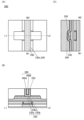
本実施の形態では、半導体装置の一形態を、図5乃至図7を用いて説明する。
以下では、本発明の一態様に係るトランジスタ200を有する半導体装置の一例について説明する。図5(A)、図5(B)、および図5(C)は、本発明の一態様に係るトランジスタ200、およびトランジスタ200周辺の上面図および断面図である。図5(A)は上面図であり、図5(B)は、図5(A)に示す一点鎖線L1-L2に対応する断面図であり、図5(C)は、図5(A)に示す一点鎖線W1-W2に対応する断面図である。なお、図5(A)の上面図では、図の明瞭化のために一部の要素を省いている。
図6には、トランジスタ200を有する半導体装置の一例を示す。図6(A)は半導体装置の上面を示す。なお、図の明瞭化のため、図6(A)において一部の膜は省略されている。また、図6(B)は、図6(A)に示す一点鎖線L1-L2に対応する断面図であり、図6(C)は、図6(A)に示す一点鎖線W1-W2に対応する断面図である。
図7には、トランジスタ200を有する半導体装置の一例を示す。図7(A)は半導体装置の上面を示す。なお、図の明瞭化のため、図7(A)において一部の膜は省略されている。また、図7(B)は、図7(A)に示す一点鎖線L1-L2に対応する断面図であり、図7(C)は、図7(A)に示す一点鎖線W1-W2に対応する断面図である。
本実施の形態では、半導体装置の一形態を、図8乃至図16を用いて説明する。なお、本実施の形態に示す半導体装置において、先の実施の形態に示した半導体装置を構成する構造と同機能を有する構造には、同符号を付記する。また、先の実施の形態に示した半導体装置の構成と共通する、本実施の形態に示す半導体装置の構成の詳細、および、同符号を付記した構造の詳細は、先の実施の形態の記載を参酌できる。
以下では、本発明の一態様に係るトランジスタ200を有する半導体装置の一例について説明する。図8(A)、図8(B)、および図8(C)は、本発明の一態様に係るトランジスタ200、およびトランジスタ200周辺の上面図および断面図である。図8(A)は上面図であり、図8(B)は、図8(A)に示す一点鎖線L1-L2に対応する断面図であり、図8(C)は、図8(A)に示す一点鎖線W1-W2に対応する断面図である。なお、図8(A)の上面図では、図の明瞭化のために一部の要素を省いている。
次に、図8に示す、本発明に係るトランジスタ200を有する半導体装置について、作製方法を図9乃至図16を用いて説明する。また、図9乃至図16において、各図の(A)は上面図を示す。また、各図の(B)は、(A)にL1-L2の一点鎖線で示す部位に対応する断面図であり、トランジスタ200のチャネル長方向の断面図でもある。また、各図の(C)は、(A)にW1-W2の一点鎖線で示す部位に対応する断面図であり、トランジスタ200のチャネル幅方向の断面図でもある。なお、各図の(A)の上面図では、図の明瞭化のために一部の要素を省いている。
以下では、本発明の一態様に係るトランジスタ200を有する半導体装置の一例について説明する。図17(A)、図17(B)、および図17(C)は、本発明の一態様に係るトランジスタ200、およびトランジスタ200周辺の上面図および断面図である。図17(A)は上面図であり、図17(B)は、図17(A)に示す一点鎖線L1-L2に対応する断面図であり、図17(C)は、図17(A)に示す一点鎖線W1-W2に対応する断面図である。なお、図17(A)の上面図では、図の明瞭化のために一部の要素を省いている。
本実施の形態では、半導体装置の一形態を、図18乃至図26を用いて説明する。なお、本実施の形態に示す半導体装置において、先の実施の形態に示した半導体装置を構成する構造と同機能を有する構造には、同符号を付記する。また、先の実施の形態に示した半導体装置の構成と共通する、本実施の形態に示す半導体装置の構成の詳細、および、同符号を付記した構造の詳細は、先の実施の形態の記載を参酌できる。
以下では、本発明の一態様に係るトランジスタ200を有する半導体装置の一例について説明する。図18(A)、図18(B)、および図18(C)は、本発明の一態様に係るトランジスタ200、およびトランジスタ200周辺の上面図および断面図である。図18(A)は上面図であり、図18(B)は、図18(A)に示す一点鎖線L1-L2に対応する断面図であり、図18(C)は、図18(A)に示す一点鎖線W1-W2に対応する断面図である。なお、図18(A)の上面図では、図の明瞭化のために一部の要素を省いている。
以下では、図18に示す、本発明に係るトランジスタ200を有する半導体装置について、作製方法を図19乃至図26を用いて説明する。また、図19乃至図26において、各図の(A)は上面図を示す。また、各図の(B)は、各図の(A)に示すL1-L2の一点鎖線で示す部位に対応する断面図であり、トランジスタ200のチャネル長方向の断面図でもある。また、各図の(C)は、各図の(A)にW1-W2の一点鎖線で示す部位に対応する断面図であり、トランジスタ200のチャネル幅方向の断面図でもある。なお、各図の(A)の上面図では、図の明瞭化のために一部の要素を省いている。
以下では、本発明の一態様に係るトランジスタ200を有する半導体装置の一例について説明する。図27(A)、図27(B)、および図27(C)は、本発明の一態様に係るトランジスタ200、およびトランジスタ200周辺の上面図および断面図である。図27(A)は上面図であり、図27(B)は、図27(A)に示す一点鎖線L1-L2に対応する断面図であり、図27(C)は、図27(A)に示す一点鎖線W1-W2に対応する断面図である。なお、図27(A)の上面図では、図の明瞭化のために一部の要素を省いている。
本実施の形態では、図28および図29を用いて、本発明の一態様に係る、酸化物を半導体に用いたトランジスタ(以下、OSトランジスタと呼ぶ場合がある。)、および容量素子が適用されている記憶装置(以下、OSメモリ装置と呼ぶ場合がある。)について説明する。OSメモリ装置は、少なくとも容量素子と、容量素子の充放電を制御するOSトランジスタを有する記憶装置である。OSトランジスタのオフ電流は極めて小さいので、OSメモリ装置は優れた保持特性をもち、不揮発性メモリとして機能させることができる。
図28(A)にOSメモリ装置の構成の一例を示す。記憶装置1400は、周辺回路1411、およびメモリセルアレイ1470を有する。周辺回路1411は、行回路1420、列回路1430、出力回路1440、およびコントロールロジック回路1460を有する。
図29(A)乃至(C)に、DRAMのメモリセルの回路構成例を示す。本明細書等において、1OSトランジスタ1容量素子型のメモリセルを用いたDRAMを、DOSRAM(登録商標)(Dynamic Oxide Semiconductor Random Access Memory)と呼ぶ場合がある。図29(A)に示す、メモリセル1471は、トランジスタM1と、容量素子CAと、を有する。なお、トランジスタM1は、ゲート(トップゲートと呼ぶ場合がある。)、及びバックゲートを有する。
図29(D)乃至(G)に、2トランジスタ1容量素子のゲインセル型のメモリセルの回路構成例を示す。図29(D)に示す、メモリセル1474は、トランジスタM2と、トランジスタM3と、容量素子CBと、を有する。なお、トランジスタM2は、ゲート(トップゲートと呼ぶ場合がある。)、及びバックゲートを有する。本明細書等において、トランジスタM2にOSトランジスタを用いたゲインセル型のメモリセルを有する記憶装置を、NOSRAM(登録商標)(Nonvolatile Oxide Semiconductor RAM)と呼ぶ場合がある。
本実施の形態では、図30を用いて、本発明の半導体装置が実装されたチップ1200の一例を示す。チップ1200には、複数の回路(システム)が実装されている。このように、複数の回路(システム)を一つのチップに集積する技術を、システムオンチップ(System on Chip:SoC)と呼ぶ場合がある。
本実施の形態では、先の実施の形態に示す半導体装置を用いた記憶装置の応用例について説明する。先の実施の形態に示す半導体装置は、例えば、各種電子機器(例えば、情報端末、コンピュータ、スマートフォン、電子書籍端末、デジタルカメラ(ビデオカメラも含む)、録画再生装置、ナビゲーションシステムなど)の記憶装置に適用できる。なお、ここで、コンピュータとは、タブレット型のコンピュータ、ノート型のコンピュータ、デスクトップ型のコンピュータの他、サーバシステムのような大型のコンピュータを含むものである。または、先の実施の形態に示す半導体装置は、メモリカード(例えば、SDカード)、USBメモリ、SSD(ソリッド・ステート・ドライブ)等の各種のリムーバブル記憶装置に適用される。図31にリムーバブル記憶装置の幾つかの構成例を模式的に示す。例えば、先の実施の形態に示す半導体装置は、パッケージングされたメモリチップに加工され、様々なストレージ装置、リムーバブルメモリに用いられる。
<電子機器>
本発明の一態様に係る半導体装置は、様々な電子機器に用いることができる。図32に、本発明の一態様に係る半導体装置を用いた電子機器の具体例を示す。
Claims (4)
- チャネル形成領域に半導体材料を有するトランジスタであって、
前記半導体材料は、金属元素と、窒素と、セリウム(Ce)と、を含む酸化物であり、
前記金属元素は、インジウム(In)と、元素M(Mはアルミニウム(Al)、ガリウム(Ga)、イットリウム(Y)又は錫(Sn))と、亜鉛(Zn)と、であり、
前記窒素は、前記酸化物の酸素欠損内に取り込まれている又は前記金属元素の原子と結合しており、
前記半導体材料中の窒素濃度は、前記半導体材料中の水素濃度以上である、トランジスタ。 - チャネル形成領域に半導体材料を有するトランジスタであって、
前記半導体材料は、金属元素と、窒素と、セリウム(Ce)と、を含む酸化物であり、
前記金属元素は、インジウム(In)と、元素M(Mはアルミニウム(Al)、ガリウム(Ga)、イットリウム(Y)又は錫(Sn))と、亜鉛(Zn)と、であり、
前記窒素は、前記酸化物の酸素欠損内に取り込まれている又は前記金属元素の原子と結合しており、
前記窒素を含む前記半導体材料は、結晶性を有する、トランジスタ。 - 請求項1または請求項2において、
前記酸化物のキャリア濃度は、5×1017cm-3未満である、トランジスタ。 - 請求項1乃至請求項3のいずれか一において、
前記酸化物に対して電子を照射した場合において、
前記電子の累積照射線量が3.6×10⁸e-/nm2以下である場合に、前記酸化物の構造変化が観察されない、トランジスタ。
Applications Claiming Priority (12)
| Application Number | Priority Date | Filing Date | Title |
|---|---|---|---|
| JP2017225439 | 2017-11-24 | ||
| JP2017225439 | 2017-11-24 | ||
| JP2017231456 | 2017-12-01 | ||
| JP2017231531 | 2017-12-01 | ||
| JP2017231456 | 2017-12-01 | ||
| JP2017231457 | 2017-12-01 | ||
| JP2017231457 | 2017-12-01 | ||
| JP2017231532 | 2017-12-01 | ||
| JP2017231531 | 2017-12-01 | ||
| JP2017231532 | 2017-12-01 | ||
| PCT/IB2018/058981 WO2019102314A1 (ja) | 2017-11-24 | 2018-11-15 | 半導体材料、および半導体装置 |
| JP2019555090A JP7190443B2 (ja) | 2017-11-24 | 2018-11-15 | 半導体材料 |
Related Parent Applications (1)
| Application Number | Title | Priority Date | Filing Date |
|---|---|---|---|
| JP2019555090A Division JP7190443B2 (ja) | 2017-11-24 | 2018-11-15 | 半導体材料 |
Publications (2)
| Publication Number | Publication Date |
|---|---|
| JP2023014361A JP2023014361A (ja) | 2023-01-26 |
| JP7493576B2 true JP7493576B2 (ja) | 2024-05-31 |
Family
ID=66631919
Family Applications (2)
| Application Number | Title | Priority Date | Filing Date |
|---|---|---|---|
| JP2019555090A Active JP7190443B2 (ja) | 2017-11-24 | 2018-11-15 | 半導体材料 |
| JP2022194011A Active JP7493576B2 (ja) | 2017-11-24 | 2022-12-05 | トランジスタ |
Family Applications Before (1)
| Application Number | Title | Priority Date | Filing Date |
|---|---|---|---|
| JP2019555090A Active JP7190443B2 (ja) | 2017-11-24 | 2018-11-15 | 半導体材料 |
Country Status (4)
| Country | Link |
|---|---|
| US (1) | US11610997B2 (ja) |
| JP (2) | JP7190443B2 (ja) |
| CN (1) | CN111373515B (ja) |
| WO (1) | WO2019102314A1 (ja) |
Families Citing this family (5)
| Publication number | Priority date | Publication date | Assignee | Title |
|---|---|---|---|---|
| WO2019130161A1 (ja) * | 2017-12-27 | 2019-07-04 | 株式会社半導体エネルギー研究所 | 半導体装置、および半導体装置の作製方法 |
| US20220383657A1 (en) * | 2019-10-04 | 2022-12-01 | Semiconductor Energy Laboratory Co., Ltd. | Semiconductor device and determination system |
| JP7778703B2 (ja) * | 2020-08-27 | 2025-12-02 | 株式会社半導体エネルギー研究所 | 半導体装置の作製方法 |
| CN114201907B (zh) * | 2020-09-18 | 2025-08-12 | 上海交通大学 | 快速预测金属化合物高精度导电特性的机器学习方法 |
| KR102869176B1 (ko) * | 2022-06-24 | 2025-10-13 | 한국항공대학교산학협력단 | 금속산화물 반도체 도핑 방법 및 이에 의해 제조되는 금속산화물 반도체 |
Citations (10)
| Publication number | Priority date | Publication date | Assignee | Title |
|---|---|---|---|---|
| JP2012114421A (ja) | 2010-11-05 | 2012-06-14 | Semiconductor Energy Lab Co Ltd | 半導体装置及び半導体装置の作製方法 |
| JP2012164978A (ja) | 2011-01-20 | 2012-08-30 | Semiconductor Energy Lab Co Ltd | 酸化物半導体素子及び半導体装置 |
| JP2012238826A (ja) | 2010-07-02 | 2012-12-06 | Semiconductor Energy Lab Co Ltd | 半導体装置 |
| JP2013179286A (ja) | 2012-02-07 | 2013-09-09 | Semiconductor Energy Lab Co Ltd | 半導体装置の作製方法 |
| JP2014056945A (ja) | 2012-09-12 | 2014-03-27 | Idemitsu Kosan Co Ltd | アモルファス酸化物薄膜及びその製造方法、並びにそれを用いた薄膜トランジスタ |
| JP2015119174A (ja) | 2013-11-15 | 2015-06-25 | 株式会社半導体エネルギー研究所 | 半導体装置及び表示装置 |
| JP2015201656A (ja) | 2010-08-27 | 2015-11-12 | 株式会社半導体エネルギー研究所 | 光センサ |
| JP2016072623A (ja) | 2014-09-26 | 2016-05-09 | 株式会社半導体エネルギー研究所 | 撮像装置 |
| US20170037505A1 (en) | 2015-08-06 | 2017-02-09 | Tsinghua University | Sputtering target, oxide semiconducting film, and method for making the same |
| JP2017034051A (ja) | 2015-07-31 | 2017-02-09 | 株式会社半導体エネルギー研究所 | 半導体装置、モジュールおよび電子機器 |
Family Cites Families (12)
| Publication number | Priority date | Publication date | Assignee | Title |
|---|---|---|---|---|
| US7994508B2 (en) * | 2007-08-02 | 2011-08-09 | Applied Materials, Inc. | Thin film transistors using thin film semiconductor materials |
| JP5387248B2 (ja) | 2009-09-07 | 2014-01-15 | 住友電気工業株式会社 | 半導体酸化物薄膜 |
| JP6013685B2 (ja) * | 2011-07-22 | 2016-10-25 | 株式会社半導体エネルギー研究所 | 半導体装置 |
| US9178042B2 (en) * | 2013-01-08 | 2015-11-03 | Globalfoundries Inc | Crystalline thin-film transistor |
| JP2015018959A (ja) | 2013-07-11 | 2015-01-29 | 出光興産株式会社 | 酸化物半導体及び酸化物半導体膜の製造方法 |
| JP6402017B2 (ja) | 2013-12-26 | 2018-10-10 | 株式会社半導体エネルギー研究所 | 半導体装置 |
| TWI718125B (zh) | 2015-03-03 | 2021-02-11 | 日商半導體能源研究所股份有限公司 | 半導體裝置及其製造方法 |
| US9917209B2 (en) | 2015-07-03 | 2018-03-13 | Semiconductor Energy Laboratory Co., Ltd. | Manufacturing method of semiconductor device including step of forming trench over semiconductor |
| WO2017055971A1 (en) * | 2015-10-01 | 2017-04-06 | Semiconductor Energy Laboratory Co., Ltd. | Display device and manufacturing method thereof |
| JP6970511B2 (ja) * | 2016-02-12 | 2021-11-24 | 株式会社半導体エネルギー研究所 | トランジスタ |
| WO2017163146A1 (en) * | 2016-03-22 | 2017-09-28 | Semiconductor Energy Laboratory Co., Ltd. | Semiconductor device and display device including the same |
| JP7200121B2 (ja) * | 2017-11-09 | 2023-01-06 | 株式会社半導体エネルギー研究所 | 半導体装置 |
-
2018
- 2018-11-15 JP JP2019555090A patent/JP7190443B2/ja active Active
- 2018-11-15 WO PCT/IB2018/058981 patent/WO2019102314A1/ja not_active Ceased
- 2018-11-15 US US16/759,020 patent/US11610997B2/en active Active
- 2018-11-15 CN CN201880075796.3A patent/CN111373515B/zh active Active
-
2022
- 2022-12-05 JP JP2022194011A patent/JP7493576B2/ja active Active
Patent Citations (10)
| Publication number | Priority date | Publication date | Assignee | Title |
|---|---|---|---|---|
| JP2012238826A (ja) | 2010-07-02 | 2012-12-06 | Semiconductor Energy Lab Co Ltd | 半導体装置 |
| JP2015201656A (ja) | 2010-08-27 | 2015-11-12 | 株式会社半導体エネルギー研究所 | 光センサ |
| JP2012114421A (ja) | 2010-11-05 | 2012-06-14 | Semiconductor Energy Lab Co Ltd | 半導体装置及び半導体装置の作製方法 |
| JP2012164978A (ja) | 2011-01-20 | 2012-08-30 | Semiconductor Energy Lab Co Ltd | 酸化物半導体素子及び半導体装置 |
| JP2013179286A (ja) | 2012-02-07 | 2013-09-09 | Semiconductor Energy Lab Co Ltd | 半導体装置の作製方法 |
| JP2014056945A (ja) | 2012-09-12 | 2014-03-27 | Idemitsu Kosan Co Ltd | アモルファス酸化物薄膜及びその製造方法、並びにそれを用いた薄膜トランジスタ |
| JP2015119174A (ja) | 2013-11-15 | 2015-06-25 | 株式会社半導体エネルギー研究所 | 半導体装置及び表示装置 |
| JP2016072623A (ja) | 2014-09-26 | 2016-05-09 | 株式会社半導体エネルギー研究所 | 撮像装置 |
| JP2017034051A (ja) | 2015-07-31 | 2017-02-09 | 株式会社半導体エネルギー研究所 | 半導体装置、モジュールおよび電子機器 |
| US20170037505A1 (en) | 2015-08-06 | 2017-02-09 | Tsinghua University | Sputtering target, oxide semiconducting film, and method for making the same |
Also Published As
| Publication number | Publication date |
|---|---|
| JPWO2019102314A1 (ja) | 2020-11-26 |
| CN111373515B (zh) | 2024-03-05 |
| CN111373515A (zh) | 2020-07-03 |
| JP2023014361A (ja) | 2023-01-26 |
| JP7190443B2 (ja) | 2022-12-15 |
| US11610997B2 (en) | 2023-03-21 |
| WO2019102314A1 (ja) | 2019-05-31 |
| US20210119052A1 (en) | 2021-04-22 |
Similar Documents
| Publication | Publication Date | Title |
|---|---|---|
| JP7493576B2 (ja) | トランジスタ | |
| JP7472340B2 (ja) | トランジスタ | |
| JP7245371B2 (ja) | 半導体装置 | |
| JP7732011B2 (ja) | 半導体装置 | |
| JP7705509B2 (ja) | 半導体装置 | |
| JPWO2019111096A1 (ja) | 半導体装置、および半導体装置の作製方法 | |
| JP2025179206A (ja) | 半導体装置の作製方法 | |
| JP7686686B2 (ja) | 半導体装置 | |
| JP2025065417A (ja) | 半導体装置 | |
| JP7462712B2 (ja) | 半導体装置 | |
| JP2025061743A (ja) | 半導体装置 | |
| JP7549639B2 (ja) | 半導体装置 | |
| JPWO2019155329A1 (ja) | 半導体装置、及び半導体装置の作製方法 | |
| JPWO2019145807A1 (ja) | 半導体装置、および半導体装置の作製方法 | |
| JPWO2018167588A1 (ja) | 半導体装置、および半導体装置の作製方法 | |
| JPWO2019207411A1 (ja) | 半導体装置、および半導体装置の作製方法 | |
| JP2019087713A (ja) | 半導体装置、および半導体装置の作製方法 | |
| JP7046692B2 (ja) | 半導体装置 | |
| WO2019111095A1 (ja) | 半導体材料、および半導体装置 | |
| JP2018152399A (ja) | 半導体装置、および半導体装置の作製方法 | |
| JPWO2019145813A1 (ja) | 半導体装置、および半導体装置の作製方法 |
Legal Events
| Date | Code | Title | Description |
|---|---|---|---|
| A621 | Written request for application examination |
Free format text: JAPANESE INTERMEDIATE CODE: A621 Effective date: 20221206 |
|
| A977 | Report on retrieval |
Free format text: JAPANESE INTERMEDIATE CODE: A971007 Effective date: 20240118 |
|
| A131 | Notification of reasons for refusal |
Free format text: JAPANESE INTERMEDIATE CODE: A131 Effective date: 20240213 |
|
| A521 | Request for written amendment filed |
Free format text: JAPANESE INTERMEDIATE CODE: A523 Effective date: 20240409 |
|
| TRDD | Decision of grant or rejection written | ||
| A01 | Written decision to grant a patent or to grant a registration (utility model) |
Free format text: JAPANESE INTERMEDIATE CODE: A01 Effective date: 20240423 |
|
| A61 | First payment of annual fees (during grant procedure) |
Free format text: JAPANESE INTERMEDIATE CODE: A61 Effective date: 20240521 |
|
| R150 | Certificate of patent or registration of utility model |
Ref document number: 7493576 Country of ref document: JP Free format text: JAPANESE INTERMEDIATE CODE: R150 |