JP7464022B2 - Test method - Google Patents
Test method Download PDFInfo
- Publication number
- JP7464022B2 JP7464022B2 JP2021142737A JP2021142737A JP7464022B2 JP 7464022 B2 JP7464022 B2 JP 7464022B2 JP 2021142737 A JP2021142737 A JP 2021142737A JP 2021142737 A JP2021142737 A JP 2021142737A JP 7464022 B2 JP7464022 B2 JP 7464022B2
- Authority
- JP
- Japan
- Prior art keywords
- under test
- semiconductor device
- time
- device under
- test
- Prior art date
- Legal status (The legal status is an assumption and is not a legal conclusion. Google has not performed a legal analysis and makes no representation as to the accuracy of the status listed.)
- Active
Links
- 238000010998 test method Methods 0.000 title claims description 17
- 239000004065 semiconductor Substances 0.000 claims description 222
- 238000012360 testing method Methods 0.000 claims description 178
- 230000007547 defect Effects 0.000 claims description 31
- 238000011156 evaluation Methods 0.000 claims description 17
- 230000001939 inductive effect Effects 0.000 claims description 15
- 238000000034 method Methods 0.000 claims description 10
- 230000002950 deficient Effects 0.000 claims description 4
- 238000010586 diagram Methods 0.000 description 10
- 239000000758 substrate Substances 0.000 description 10
- 238000001514 detection method Methods 0.000 description 8
- 239000012535 impurity Substances 0.000 description 5
- 239000003990 capacitor Substances 0.000 description 4
- 230000005540 biological transmission Effects 0.000 description 3
- 230000007423 decrease Effects 0.000 description 3
- 229910052782 aluminium Inorganic materials 0.000 description 2
- XAGFODPZIPBFFR-UHFFFAOYSA-N aluminium Chemical compound [Al] XAGFODPZIPBFFR-UHFFFAOYSA-N 0.000 description 2
- 230000003111 delayed effect Effects 0.000 description 2
- 230000006698 induction Effects 0.000 description 2
- 239000007769 metal material Substances 0.000 description 2
- 238000012986 modification Methods 0.000 description 2
- 230000004048 modification Effects 0.000 description 2
- 239000011347 resin Substances 0.000 description 2
- 229920005989 resin Polymers 0.000 description 2
- 230000008859 change Effects 0.000 description 1
- 230000005484 gravity Effects 0.000 description 1
- 238000004519 manufacturing process Methods 0.000 description 1
- 239000000463 material Substances 0.000 description 1
- 238000005259 measurement Methods 0.000 description 1
- 229910021420 polycrystalline silicon Inorganic materials 0.000 description 1
- 229920005591 polysilicon Polymers 0.000 description 1
- 230000008569 process Effects 0.000 description 1
- 230000004044 response Effects 0.000 description 1
- 239000000523 sample Substances 0.000 description 1
- 229910052710 silicon Inorganic materials 0.000 description 1
- 239000010703 silicon Substances 0.000 description 1
- 230000000087 stabilizing effect Effects 0.000 description 1
Images


Classifications
-
- G—PHYSICS
- G01—MEASURING; TESTING
- G01R—MEASURING ELECTRIC VARIABLES; MEASURING MAGNETIC VARIABLES
- G01R31/00—Arrangements for testing electric properties; Arrangements for locating electric faults; Arrangements for electrical testing characterised by what is being tested not provided for elsewhere
- G01R31/28—Testing of electronic circuits, e.g. by signal tracer
- G01R31/2851—Testing of integrated circuits [IC]
- G01R31/2894—Aspects of quality control [QC]
-
- G—PHYSICS
- G01—MEASURING; TESTING
- G01R—MEASURING ELECTRIC VARIABLES; MEASURING MAGNETIC VARIABLES
- G01R31/00—Arrangements for testing electric properties; Arrangements for locating electric faults; Arrangements for electrical testing characterised by what is being tested not provided for elsewhere
- G01R31/26—Testing of individual semiconductor devices
- G01R31/27—Testing of devices without physical removal from the circuit of which they form part, e.g. compensating for effects surrounding elements
- G01R31/275—Testing of devices without physical removal from the circuit of which they form part, e.g. compensating for effects surrounding elements for testing individual semiconductor components within integrated circuits
-
- G—PHYSICS
- G01—MEASURING; TESTING
- G01R—MEASURING ELECTRIC VARIABLES; MEASURING MAGNETIC VARIABLES
- G01R31/00—Arrangements for testing electric properties; Arrangements for locating electric faults; Arrangements for electrical testing characterised by what is being tested not provided for elsewhere
- G01R31/26—Testing of individual semiconductor devices
- G01R31/2607—Circuits therefor
- G01R31/2608—Circuits therefor for testing bipolar transistors
- G01R31/2617—Circuits therefor for testing bipolar transistors for measuring switching properties thereof
-
- G—PHYSICS
- G01—MEASURING; TESTING
- G01R—MEASURING ELECTRIC VARIABLES; MEASURING MAGNETIC VARIABLES
- G01R31/00—Arrangements for testing electric properties; Arrangements for locating electric faults; Arrangements for electrical testing characterised by what is being tested not provided for elsewhere
- G01R31/28—Testing of electronic circuits, e.g. by signal tracer
- G01R31/2851—Testing of integrated circuits [IC]
- G01R31/2855—Environmental, reliability or burn-in testing
- G01R31/2856—Internal circuit aspects, e.g. built-in test features; Test chips; Measuring material aspects, e.g. electro migration [EM]
-
- G—PHYSICS
- G01—MEASURING; TESTING
- G01R—MEASURING ELECTRIC VARIABLES; MEASURING MAGNETIC VARIABLES
- G01R31/00—Arrangements for testing electric properties; Arrangements for locating electric faults; Arrangements for electrical testing characterised by what is being tested not provided for elsewhere
- G01R31/28—Testing of electronic circuits, e.g. by signal tracer
- G01R31/2832—Specific tests of electronic circuits not provided for elsewhere
- G01R31/2836—Fault-finding or characterising
- G01R31/2837—Characterising or performance testing, e.g. of frequency response
Landscapes
- Engineering & Computer Science (AREA)
- Microelectronics & Electronic Packaging (AREA)
- Physics & Mathematics (AREA)
- General Physics & Mathematics (AREA)
- Computer Hardware Design (AREA)
- General Engineering & Computer Science (AREA)
- Environmental & Geological Engineering (AREA)
- Testing Of Individual Semiconductor Devices (AREA)
Description
本発明は、半導体装置の試験方法に関する。 The present invention relates to a method for testing semiconductor devices.
従来、トランジスタ等の半導体装置を試験する方法が知られている(例えば、特許文献1参照)。
特許文献1 特開2010-276477号公報
2. Description of the Related Art Conventionally, a method for testing a semiconductor device such as a transistor is known (see, for example, Japanese Patent Application Laid-Open No. 2003-233663).
Patent Document 1: JP 2010-276477 A
半導体装置を精度よく試験できることが好ましい。 It is preferable to be able to test semiconductor devices with high accuracy.
上記課題を解決するために、本発明の一つの態様においては、被試験半導体装置の試験方法を提供する。試験方法は、1つ以上の被試験半導体装置に制御信号を入力して、被試験半導体装置をオン状態に制御するオン段階を備えてよい。試験方法は、オン状態の被試験半導体装置をオフ状態に制御したときの被試験半導体装置を観測して、被試験半導体装置を評価する評価段階を備えてよい。オン段階において、1つの被試験半導体装置における複数の領域の間、または、複数の被試験半導体装置の間における制御信号の遅延時間のばらつきの大きさに基づいて、被試験半導体装置をオン状態にするオン時間の長さを調整してよい。 In order to solve the above problems, one aspect of the present invention provides a method for testing semiconductor devices under test. The test method may include an ON stage in which a control signal is input to one or more semiconductor devices under test to control the semiconductor devices under test to an ON state. The test method may include an evaluation stage in which the semiconductor devices under test are observed when the semiconductor devices under test in an ON state are controlled to an OFF state, and the semiconductor devices under test are evaluated. In the ON stage, the length of the ON time for turning the semiconductor devices under test into an ON state may be adjusted based on the magnitude of variation in delay time of the control signal between multiple regions in one semiconductor device under test or between multiple semiconductor devices under test .
オン段階において、制御信号の遅延時間の最大値に基づいて、オン状態の時間を調整してよい。 During the on phase, the on-state time may be adjusted based on the maximum delay time of the control signal.
遅延時間のばらつきが大きいほど、オン時間を長くしてよい。 The greater the variation in delay time, the longer the on time can be.
被試験半導体装置をオン状態に制御してから、複数の領域に流れる電流、または、複数の被試験半導体装置に流れる電流のばらつきが一定値以下となるまでの時間に応じて、被試験半導体装置に直列に接続される誘導成分を調整してよい。 The inductive component connected in series to the semiconductor device under test may be adjusted according to the time from when the semiconductor device under test is controlled to the on state until the variation in the current flowing through the multiple regions or the current flowing through the multiple semiconductor devices under test falls to a certain value or less.
電流のばらつきが一定値以下となるまでのタイミング以降に、被試験半導体装置に流れる電流が予め定められた試験電流の値に到達するように、誘導成分を調整してよい。 The inductive component may be adjusted so that the current flowing through the semiconductor device under test reaches a predetermined test current value after the current variation falls below a certain value.
試験方法は、評価段階において良品と判定されたチップ状態の被試験半導体装置をモジュールに組み込んだ場合に、モジュールにおける不良率を取得するモジュール不良取得段階を備えてよい。オン段階では、モジュールの不良率に基づいて、オン時間を調整してよい。 The test method may include a module defect acquisition stage in which a defect rate in the module is acquired when a semiconductor device under test in a chip state determined to be a good product in the evaluation stage is incorporated into a module. In the on stage, the on time may be adjusted based on the defect rate of the module.
オン段階において、オン時間を100μs以上に設定してよい。 In the on phase, the on time may be set to 100 μs or more.
オン段階において、オン時間が経過したときの被試験半導体装置の面内における電流ばらつきが20%以下となるように、オン時間を設定してよい。 In the on-stage, the on-time may be set so that the current variation within the plane of the semiconductor device under test when the on-time has elapsed is 20% or less.
予め欠陥を形成した複数の参照半導体装置に対して、オン時間を変動させてオン段階を行ってよい。複数の参照半導体装置に対する評価段階における不良率が基準値以上となるオン時間を検出してよい。検出したオン時間に基づいて、被試験半導体装置に対するオン段階におけるオン時間を調整してよい。 The on-phase may be performed by varying the on-time for a plurality of reference semiconductor devices in which defects have been formed in advance. The on-time at which the failure rate in the evaluation phase for the plurality of reference semiconductor devices is equal to or greater than a reference value may be detected. The on-time in the on-phase for the semiconductor device under test may be adjusted based on the detected on-time.
なお、上記の発明の概要は、本発明の必要な特徴の全てを列挙したものではない。また、これらの特徴群のサブコンビネーションもまた、発明となりうる。 Note that the above summary of the invention does not list all of the necessary features of the present invention. Also, subcombinations of these features may also be inventions.
以下、発明の実施の形態を通じて本発明を説明するが、以下の実施形態は特許請求の範囲にかかる発明を限定するものではない。また、実施形態の中で説明されている特徴の組み合わせの全てが発明の解決手段に必須であるとは限らない。 The present invention will be described below through embodiments of the invention, but the following embodiments do not limit the invention according to the claims. Furthermore, not all of the combinations of features described in the embodiments are necessarily essential to the solution of the invention.
本明細書においては半導体基板(または半導体装置)の深さ方向と平行な方向における一方の側を「上」、他方の側を「下」と称する。基板、層またはその他の部材の2つの主面のうち、一方の面を上面、他方の面を下面と称する。「上」、「下」の方向は、重力方向または半導体装置の実装時における方向に限定されない。 In this specification, one side in a direction parallel to the depth direction of a semiconductor substrate (or semiconductor device) is referred to as "upper" and the other side as "lower." Of the two main surfaces of a substrate, layer, or other member, one surface is referred to as the upper surface and the other surface is referred to as the lower surface. The directions of "upper" and "lower" are not limited to the direction of gravity or the directions when the semiconductor device is mounted.
本明細書において「同一」または「等しい」のように称した場合、製造ばらつき等に起因する誤差を有する場合も含んでよい。当該誤差は、例えば10%以内である。 In this specification, when we say "same" or "equal," it may include cases where there is an error due to manufacturing variations, etc. The error is, for example, within 10%.
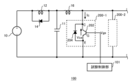
図1は、本発明の一つの実施形態に係る、半導体装置200を試験する試験装置100の概要を示す図である。本例の半導体装置200は、トランジスタ部202およびダイオード部204を含む。トランジスタ部202は、例えばIGBT(Insulated Gate Bipolar Transistor)素子を含むが、他のトランジスタを含んでもよい。ダイオード部204は、トランジスタ部202と逆並列に接続された環流ダイオードである。本例の半導体装置200は、いわゆる逆導通IGBT(RC-IGBT)である。本明細書においては、トランジスタ部202のコレクタ端子Cに流れる電流をIc、トランジスタ部202のエミッタ端子Eとコレクタ端子C間の電圧をVce、トランジスタ部202のゲート端子Gに印加される電圧をVgeとする。
FIG. 1 is a diagram showing an overview of a
試験装置100は、1つ以上の半導体装置200(本明細書では、被試験半導体装置と称する場合がある)を試験する。1つの半導体装置200は、トランジスタ部202およびダイオード部204を含む1つのチップから構成されてよく、トランジスタ部202を含むチップとダイオード部204を含むチップの2つのチップから構成されてもよい。半導体装置200を試験する際には、複数のチップが形成されたウエハの状態であってよく、ウエハから切り出されたチップの状態であってもよい。さらには、1つ以上の半導体装置200と半導体装置200に接続される配線および端子とを、樹脂等のケース内に収容した装置(モジュール)、の状態であってもよい。試験装置100には、複数の半導体装置200(200-1,200-2)が並列に接続されてよい。例えば、モジュールの状態において、モジュール内に配置された並列に接続されている複数の半導体装置200がある。試験装置100は、半導体装置200に所定の条件で電圧および電流を供給し、半導体装置200の動作に基づいて、半導体装置200の良否を判定する。試験装置100は、半導体装置200における電圧Vceおよび電流Icの少なくとも一方を測定してよい。
The
試験装置100は、試験制御部101、電源10、コンデンサ11、コイル12、コイル16およびダイオード14を有する。試験制御部101は、それぞれの半導体装置200にゲート電圧Vgeを供給する。試験制御部101は、同一のゲート電圧Vgeを、複数の半導体装置200に印加してよい。また、試験制御部101は、それぞれの半導体装置200の電圧Vceおよび電流Icを測定してよい。
The
電源10は、1つ以上の半導体装置200に供給する電力を生成する。コンデンサ11は、電源安定用のコンデンサである。コイル12は、電源10と、半導体装置200のコレクタ端子との間に配置されている。コイル16は、コイル12と、半導体装置200のコレクタ端子との間に配置されている。ダイオード14は、コイル12と並列に接続されている。ダイオード14は、半導体装置200をターンオフさせたときに、半導体装置200に流れていた電流を電源10側に環流する。コイル12、コイル16およびダイオード14は、複数の半導体装置200に対して共通に設けられてよい。
The
また、コイル16は、誘導成分の値が調整可能であってよい。例えば試験装置100は、誘導成分の値が異なる複数のコイル16を並列に備えており、且つ、コイル12および半導体装置200の間に接続するコイル16を選択するスイッチを備えてよい。コイル16の誘導成分を調整することで、半導体装置200の電流Icの波形の傾きを調整できる。
The value of the inductive component of the
本例の試験制御部101は、半導体装置200をターンオフさせたときの半導体装置200の動作に基づいて、半導体装置200の良否を判定する。試験制御部101は、半導体装置200の電流Icおよび電圧Vceの少なくとも一方の波形に基づいて、半導体装置200の良否を判定してよい。
The
本例の試験制御部101は、半導体装置200の逆バイアス安全動作領域(RBSOA)を試験する。本例の試験制御部101は、所定の試験電流が流れている半導体装置200をターンオフさせたときの電流Icおよび電圧Vceが、所定の範囲内で推移するか否かを判定してよい。試験制御部101は、ターンオフ時における電圧Vceのサージの大きさ等が所定の基準を満たすか否かを判定してもよい。
The
図2は、半導体装置200の上面構造の概要を示す図である。図2においてはチップ状の半導体装置200を示している。半導体装置200は、半導体基板206を有する。半導体基板206は、シリコン等の半導体材料で形成された基板である。
Figure 2 is a diagram showing an overview of the top surface structure of the
半導体基板206の上面には、上面パッド210、制御パッド208およびゲートランナー222が設けられている。上面パッド210は、トランジスタ部202のエミッタ端子Eに接続される電極である。上面パッド210の下方の半導体基板206には、トランジスタ部202およびダイオード部204が設けられている。また、半導体基板206の下面には、トランジスタ部202のコレクタ端子Cに接続される下面パッドが設けられてよい。本例の半導体装置200は、オン状態に制御されると、上面パッド210と下面パッドとの間で電流が流れる縦型デバイスである。他の例では、半導体装置200は、2つのパッドの両方が上面に配置される横型デバイスであってもよい。
The upper surface of the
制御パッド208は、トランジスタ部202のゲート端子Gに接続される電極である。制御パッド208には、試験制御部101からゲート電圧Vgeが印加される。上面パッド210および制御パッド208は、アルミニウム等の金属材料で形成されてよい。
The
ゲートランナー222は、制御パッド208と、トランジスタ部202のゲート端子Gとを接続する。ゲートランナー222は、アルミニウム等の金属材料で形成されてよく、不純物が添加されたポリシリコンで形成されてもよい。本例のゲートランナー222は、上面パッド210を囲むように配置された部分と、上面パッド210を分割するように配置された部分を有する。トランジスタ部202のゲート端子は、ゲートランナー222のいずれかの部分に接続される。
The
半導体装置200のターンオフ時の特性を試験する場合、半導体装置200の上面内において電流がほぼ均一に流れている状態で、半導体装置200をターンオフすることが好ましい。面内の電流にばらつきが生じていると、例えば電流が少ない領域ではラッチアップ等の現象を十分に観察できなくなる。
When testing the characteristics of the
半導体装置200をターンオフする前における、半導体装置200がオンしている期間が十分でないと、半導体装置200の面内の電流にばらつきが生じやすくなる。例えば、制御パッド208からのゲートランナー222の経路長によって、ゲート電圧Vgeの遅延時間にばらつきが生じ得る。このため、制御パッド208に近い領域Aでは、トランジスタ部202が早くオンし始めるのに対し、制御パッド208から遠い領域Bでは、トランジスタ部202のオンが遅れてしまう。このため、半導体装置200をオンさせてから所定の期間内は、半導体装置200の面内の電流にばらつきが生じやすくなる。
If the period during which the
図3は、参考例に係る半導体装置200のゲート電圧Vge、電流Icおよび電圧Vceの波形を示す図である。図3において横軸は時間であり、縦軸は電圧または電流の大きさを示す。
Figure 3 is a diagram showing the waveforms of the gate voltage Vge, current Ic, and voltage Vce of the
時刻t1において、半導体装置200をターンオンさせるゲート電圧Vgeを印加する。ゲート電圧Vgeに応じて電流Icが流れ始める。また、半導体装置200が導通することで、エミッタ/コレクタ間の電圧Vceが低下する。
At time t1, a gate voltage Vge is applied to turn on the
ただし図2において説明したように、時刻t1から所定の期間内では、半導体装置200の面内の領域ごとに電流がばらつきやすい。図3においては、領域Aの電流Icを実線で示し、領域Bの電流Icを破線で示している。例えば領域Bのトランジスタ部202は、ゲート電圧Vgeの伝達が遅れるので、領域Aよりも電流Icが小さくなる。
However, as explained in FIG. 2, within a certain period from time t1, the current is likely to vary between regions on the surface of the
RBSOA試験では、半導体装置200に所定の試験電流I2を流した状態で、半導体装置200をターンオフさせる。試験制御部101は、半導体装置200をターンオフさせた後の電流Icおよび電圧Vceの波形に基づいて、半導体装置200が所定の電圧および電流の範囲内で動作できるかを判定する。
In the RBSOA test, the
図3の例では、時刻t1から所定のオン時間PW1が経過した時刻t2において、半導体装置200をターンオフする。しかし図3に示すように、オン時間PW1が短いと、領域Bの電流Icが所定の試験電流I2に達しておらず、領域Bのトランジスタ部202およびダイオード部204を精度よく試験できない。
In the example of FIG. 3, the
図2および図3の例では、一つの半導体装置200の面内における電流Icのばらつきを説明したが、複数の半導体装置200を並列に試験する場合においては、半導体装置200の間でも電流Icのばらつきが生じ得る。例えば、それぞれの半導体装置200に対するゲート電圧Vgeの伝送遅延にばらつきが存在する場合、それぞれの半導体装置200に流れる電流Icにばらつきが生じる。このような場合も、それぞれの半導体装置200のオン時間PW1が短いと、電流Icが所定の試験電流I2に達しない半導体装置200が存在して、当該半導体装置200を精度よく試験できない場合がある。
2 and 3, the variation in the current Ic within the plane of one
図4は、本発明の一つの実施形態に係る、半導体装置200のゲート電圧Vge、電流Icおよび電圧Vceの波形を示す図である。試験制御部101は、時刻t0において、1つ以上の半導体装置200に制御信号(本例ではゲート電圧Vge)を入力して、半導体装置200をオン状態に制御する。試験制御部101は、時刻t0から所定のオン時間PW2が経過した時刻t2で、それぞれの半導体装置200をターンオフする。試験制御部101は、ターンオフした後の半導体装置200の電圧Vceおよび電流Icが、所定の範囲内か否かにより、RBSOA試験を行う。
Figure 4 is a diagram showing waveforms of gate voltage Vge, current Ic, and voltage Vce of
本例の試験制御部101は、1つの半導体装置200における複数の領域(例えば領域A、B)の間、または、複数の半導体装置200の間における、ゲート電圧Vgeの遅延時間のばらつきの大きさに基づいて、オン時間PW2の長さを調整する。当該遅延時間のばらつきが大きいほど、半導体装置200内、または、複数の半導体装置200間の電流Icがほぼ均一になるまでの時間は長くなる。このため試験制御部101は、当該遅延時間のばらつきが大きいほど、オン時間PW2を長くする。
The
ゲート電圧Vgeの遅延時間のばらつきは、実際にゲート電圧Vgeの遅延時間を測定してよく、他の方法で推定してもよい。例えば半導体装置200の上面の面積が大きい場合には、面内の領域ごとのゲートランナー222の経路長の差異が大きくなるので、遅延時間のばらつきが大きくなると推定できる。
The variation in the delay time of the gate voltage Vge may be estimated by actually measuring the delay time of the gate voltage Vge or by other methods. For example, if the area of the top surface of the
また、予め欠陥を作りこんだ参照用の半導体装置に対して、オン時間PWを変化させて試験を行い、オン時間PW毎の不良検出率(不良を検出できた割合)から、遅延時間のばらつきの大きさを推定してもよい。例えば、遅延時間のばらつきに対して、十分長いオン時間PWを設定できている場合には、予め欠陥を作りこんだ参照用半導体装置に対する不良検出率がほぼ100%になる。一方で、遅延時間のばらつきに対してオン時間PWが十分でない場合には、不良検出率が低下する。従って、所定の不良検出率を実現できるオン時間PWの大きさを検出することで、遅延時間のばらつきの大きさを評価できる。 In addition, a reference semiconductor device in which defects have been engineered in advance may be tested by varying the on-time PW, and the magnitude of the variation in delay time may be estimated from the defect detection rate (the proportion of defects that can be detected) for each on-time PW. For example, if a sufficiently long on-time PW can be set relative to the variation in delay time, the defect detection rate for the reference semiconductor device in which defects have been engineered in advance will be nearly 100%. On the other hand, if the on-time PW is not sufficient relative to the variation in delay time, the defect detection rate will decrease. Therefore, the magnitude of the variation in delay time can be evaluated by detecting the magnitude of the on-time PW that can achieve a specified defect detection rate.
図4の例では、時刻t3において領域Aの電流Icと、領域Bの電流Icとがほぼ均一になる。このように、ターンオンしてから、半導体装置200の面内の電流Ic(または、複数の半導体装置200間の電流Ic)が均一になるまでの時間をTとする。電流が均一とは、例えば電流値のばらつきが20%以下である状態を指す。時間Tは、遅延時間のばらつきの大きさに応じて変化する。試験制御部101は、オン時間PW2を時間T以上にすることで、ターンオフのタイミング(時刻t2)における、半導体装置200の各領域または各半導体装置200の電流Icを均一化する。これにより、半導体装置200の試験を精度よく実施できる。試験制御部101は、オン時間PW2を100μs以上に設定してよく、130μs以上に設定してもよい。試験制御部101は、オン時間PW2を150μs以下に設定してよい。オン時間PW2を、時間Tよりも長くしすぎると、試験の効率が低下してしまう。オン時間PW2は、時間Tの2倍以下であってよく、1.5倍以下であってよく、1.2倍以下であってもよい。
In the example of FIG. 4, the current Ic in the region A and the current Ic in the region B become almost uniform at time t3. In this way, the time from turning on until the current Ic in the plane of the semiconductor device 200 (or the current Ic between the multiple semiconductor devices 200) becomes uniform is set to T. The uniform current refers to a state in which the variation in current value is, for example, 20% or less. The time T changes depending on the magnitude of the variation in delay time. The
なお試験制御部101は、オン時間PW2内で、半導体装置200の各領域または各半導体装置200の電流Icが所定の試験電流I2に達することができるように、コイル16の誘導成分の値を調整することが好ましい。試験制御部101は、時刻t3以降の時刻t4において、半導体装置200の各領域または各半導体装置200の電流Icが、所定の試験電流I2に達することができるように、時間Tに基づいてコイル16の誘導成分の値を調整してもよい。なお、時刻t2、t3およびt4は、同一の時刻であってもよい。つまり、時刻t0から時間Tが経過したタイミングで、それぞれの電流Icが試験電流I2に到達するようにコイル16の誘導成分を調整してよい。更に、当該タイミングで半導体装置200をターンオフさせてよい。これにより、試験時間を短くできる。
Note that the
図5は、試験装置100による試験方法の概要を示すチャート図である。本例の試験方法は、図1から図4において説明した試験装置100による試験と同様である。まず遅延評価段階S500において、試験制御部101は、半導体装置200の面内、または、複数の半導体装置200の間におけるゲート電圧Vgeの遅延ばらつきを評価する。上述したように、試験制御部101は、遅延時間そのものを測定してよく、遅延ばらつきの大きさに応じて変動する他のパラメータ(例えば上述した不良検出率)を用いて、遅延時間のばらつきを評価してもよい。また、試験制御部101は、半導体装置200に流れる電流のばらつきから、遅延時間のばらつきの大きさを評価してもよい。例えば試験制御部101は、図4において説明した時間Tを測定してもよい。
Figure 5 is a chart showing an overview of the test method by the
次に誘導成分選択段階S510において試験制御部101は、S500において評価した遅延時間のばらつきの大きさに応じて、コイル16の誘導成分を選択する。上述したように試験装置100には、誘導成分の値が異なる複数のコイル16が、選択可能に設けられている。試験制御部101は、時刻t3以降に電流Icが所定の試験電流I2に達するようなコイル16を選択する。試験制御部101は、電流Icが所定の試験電流I2に達する時刻t4が、時刻t3以降で、且つ、時刻t3に最も近くなるようなコイル16を選択する。これにより、試験時間が過剰に長くなることを抑制できる。
Next, in the inductive component selection step S510, the
次にオン時間調整段階S520において試験制御部101は、電流Icが所定の試験電流I2に達する時刻t4以降に、半導体装置200をターンオフさせるように、オン時間PW2を設定する。試験制御部101は、時刻t4において半導体装置200がターンオフするようなオン時間PW2を設定してよく、時刻t4に対して所定のマージン時間が経過した時刻t2において半導体装置200がターンオフするようなオン時間PW2を設定してもよい。
Next, in the on-time adjustment step S520, the
試験制御部101は、半導体装置200におけるゲート電圧Vgeの遅延時間の最大値に基づいて、オン時間PW2を調整してよい。つまり試験制御部101は、ゲート電圧Vgeが最も遅く到達する領域でも、オン時間PW2内で他の領域と同等の電流Icが流れるように、オン時間PW2およびコイル16の誘導成分を調整してよい。試験制御部101は、オン時間PW2が経過したとき(時刻t2)の半導体装置200の面内における電流ばらつきが20%以下となるように、オン時間PW2を設定してもよい。
The
次にオン段階S530において試験制御部101は、1つ以上の半導体装置200をオン状態に制御するゲート電圧Vgeを印加する。オン段階S530においては、S510で設定したコイル16、および、S520で設定したオン時間PW2を用いて、半導体装置200をオン状態に制御する。
Next, in the ON phase S530, the
オン時間PW2が経過したタイミングで、試験制御部101は、オン状態の半導体装置200をオフ状態に制御する(オフ段階S540)。そして、評価段階S550において試験制御部101は、オン状態の半導体装置200をオフ状態に制御したときの半導体装置200を観測して、半導体装置200を評価する。例えば試験制御部101は、半導体装置200をターンオフさせた後の電圧Vceおよび電流Icが、所定の範囲内で推移するか否かに基づいて、半導体装置200の良否を判定する。
When the on-time PW2 has elapsed, the
本例の試験方法によれば、半導体装置200の面内、または、複数の半導体装置200に対してほぼ均一な電流Icを流した状態で、半導体装置200をターンオフできる。このため、半導体装置200を精度よく評価できる。
According to the test method of this example, the
図6は、試験装置100による試験方法の他の例を示すチャート図である。本例の試験方法は、図5に示した試験方法の各工程に加えて、オン時間設定段階S508およびモジュール不良取得段階S600を更に備える。
6 is a chart showing another example of the test method by the
評価段階S550において良品と判定されたチップ状態の半導体装置200は、モジュールに組み込まれる場合がある。モジュールは、1つ以上の半導体装置200と、半導体装置200に接続される配線および端子とを、樹脂等のケース内に収容した装置である。
The
モジュール不良取得段階S600においては、良品と判定された半導体装置200が組み込まれたモジュールに発生する不良率を取得する。当該不良率は、モジュールの全体の個数に対して、半導体装置200に故障が発生した故障モジュールの個数の比率である。なお、組み込まれた半導体装置200がターンオフ時に故障したモジュールを、故障モジュールとして計数してよい。モジュールでの不良率が高い場合には、オン段階S530におけるオン時間PW2が十分でない可能性が高い。試験制御部101は、モジュールでの不良率がより高い場合に、オン時間設定段階S508においてオン時間PW2をより長く設定してよい。モジュール不良率は、出荷前のモジュールを試験することで取得してよく、出荷後のモジュールが使用時に故障した比率を取得してもよい。
In the module failure acquisition step S600, a failure rate occurring in a module in which a
また、試験制御部101は、半導体装置200の複数のグループを準備し、各グループに対して異なるオン時間PW2を割り当てた状態で、S530からS550の試験を実施してよい。そして、各グループで良品と判定された半導体装置200をモジュールに組み込み、各グループにおけるモジュール良品率を取得してよい。これにより、オン時間PW2と、モジュールでの不良率との相関を取得できる。試験制御部101は、モジュールでの不良率が所定の許容範囲となるように、オン時間PW2を調整してよい。
The
図7は、遅延評価段階S500の他の例を説明するチャート図である。本例では、予め欠陥を形成した複数の参照半導体装置を準備する。参照半導体装置は、半導体装置200の試験におけるオン時間PW2を設定するために用いる装置である。参照半導体装置は、欠陥以外は半導体装置200と同一の構造を有することが好ましい。
Figure 7 is a chart illustrating another example of the delay evaluation stage S500. In this example, multiple reference semiconductor devices with defects formed in advance are prepared. The reference semiconductor devices are devices used to set the on-time PW2 in testing the
当該欠陥は、例えばRBSOA試験を実施することで、参照半導体装置が不良と判定されるような欠陥である。一例として、半導体基板206の内部に形成する不純物領域の不純物濃度を仕様値から逸脱させることで、当該欠陥を形成してよい。例えば、トランジスタ部202においてラッチアップが発生しやすくなるように、P型の不純物領域の不純物濃度を設定することで、当該欠陥を形成できる。当該欠陥は、ゲート電圧Vgeの伝送遅延時間が最大となる領域に形成してよい。
The defect in question is one that would cause the reference semiconductor device to be determined to be defective, for example, by performing an RBSOA test. As an example, the defect may be formed by causing the impurity concentration of an impurity region formed inside the
次に試験段階S504において、参照半導体装置を複数のグループに分けて、それぞれのグループ毎に異なるオン時間PWを設定する。試験段階S504では、図5におけるS530~S550と同様の試験を行う。これにより、それぞれのオン時間PWに対する、参照半導体装置の不良率を取得できる。 Next, in the test stage S504, the reference semiconductor device is divided into multiple groups, and a different on-time PW is set for each group. In the test stage S504, tests similar to S530 to S550 in FIG. 5 are performed. This makes it possible to obtain the failure rate of the reference semiconductor device for each on-time PW.
次にオン時間検出段階S506において、参照半導体装置の不良率が所定値以上となるオン時間PWを検出する。当該所定値は、90%以上であってよく、100%であってもよい。検出したオン時間PWを用いれば、欠陥を有する半導体装置200を当該不良率に応じた確率で検出できる。
Next, in the on-time detection step S506, the on-time PW at which the defect rate of the reference semiconductor device is equal to or greater than a predetermined value is detected. The predetermined value may be equal to or greater than 90%, or may be 100%. By using the detected on-time PW, a
オン時間検出段階S506で検出したオン時間PWを、半導体装置200に対するオン段階S530におけるオン時間PW2として用いてよい。また、オン時間検出段階S506で検出したオン時間PWを、電流Icがほぼ均一になるのに要する時間Tとして扱ってもよい。試験制御部101は、オン時間PWを時間Tとして、S508からS520の処理を行ってもよい。
The on-time PW detected in the on-time detection step S506 may be used as the on-time PW2 in the on-phase S530 for the
図8は、試験段階S504の一例を説明する図である。図8では、参照半導体装置の一つのグループにおける不良率を、一つの四角印でプロットしている。グラフ801に含まれるグループは、比較的にオン時間PWが短い(30μs~50μs程度)グループであり、グラフ802に含まれるグループは、比較的にオン時間PWが長い(60μs~85μs程度)グループである。また、グラフ801に含まれるグループに対しては、コイル16の誘導成分をL=200μHとし、グラフ802に含まれるグループに対しては、コイル16の誘導成分をL=400μHとしている。つまり、グラフ802に含まれるグループにおける電流Icの傾きは、グラフ801に含まれるグループにおける電流Icの傾きよりも緩やかである。
Figure 8 is a diagram illustrating an example of the test stage S504. In Figure 8, the failure rate in one group of the reference semiconductor device is plotted with one square mark. The group included in
また、それぞれのプロットの近傍に、オン時間PWが経過したときの電流Icの値を示している。同一グループでは同一のコイル16を用いているので、オン時間PWが長くなるほど電流Icは増大している。
Also, the value of the current Ic when the on-time PW has elapsed is shown near each plot. Since the
図8に示すように、オン時間PWが短いと、ターンオフ時の電流Icを大きくしても、不良率が80%にも到達していない。なおグラフ801において更にオン時間PWおよび電流Icを大きくすると、試験装置100のプローブと、参照半導体装置の電極との接触点での発熱が大きくなり、当該接触点で参照半導体装置が破壊されてしまう。
As shown in FIG. 8, when the on-time PW is short, the failure rate does not even reach 80% even if the current Ic at turn-off is increased. If the on-time PW and current Ic are further increased in
グラフ802に示すように、一定以上の誘導成分を有するコイル16を用いた場合、オン時間PWを適切に設定することで、参照半導体装置の不良率が基準値以上(例えば100%)になる。これは、電流Icが所定の試験電流(例えば190A)に到達するタイミングを、参照半導体装置の面内の電流Icがほぼ均一になるタイミングより後に設定し、且つ、電流Icが所定の試験電流に到達できるだけのオン時間PWを確保したことで、参照半導体装置の欠陥を適切に検出できたためと考えられる。
As shown in
試験制御部101は、図8に示したような測定を行い、不良率が基準値を超えるようなオン時間PWを検出してよい。試験制御部101は、検出したオン時間PWを、被試験半導体装置である半導体装置200の試験で用いてよい。これにより、半導体装置200の不良を精度よく検出できる。
The
以上、本発明を実施の形態を用いて説明したが、本発明の技術的範囲は上記実施の形態に記載の範囲には限定されない。上記実施の形態に、多様な変更または改良を加えることが可能であることが当業者に明らかである。その様な変更または改良を加えた形態も本発明の技術的範囲に含まれ得ることが、特許請求の範囲の記載から明らかである。 The present invention has been described above using an embodiment, but the technical scope of the present invention is not limited to the scope described in the above embodiment. It is clear to those skilled in the art that various modifications and improvements can be made to the above embodiment. It is clear from the claims that forms with such modifications or improvements can also be included in the technical scope of the present invention.
10・・・電源、11・・・コンデンサ、12・・・コイル、14・・・ダイオード、16・・・コイル、100・・・試験装置、101・・・試験制御部、200・・・半導体装置、202・・・トランジスタ部、204・・・ダイオード部、206・・・半導体基板、208・・・制御パッド、210・・・上面パッド、222・・・ゲートランナー、801、802・・・グラフ 10: power supply, 11: capacitor, 12: coil, 14: diode, 16: coil, 100: test device, 101: test control section, 200: semiconductor device, 202: transistor section, 204: diode section, 206: semiconductor substrate, 208: control pad, 210: upper surface pad, 222: gate runner, 801, 802: graph
Claims (11)
複数の前記被試験半導体装置に制御信号を入力して、前記被試験半導体装置をオン状態に制御するオン段階と、
オン状態の前記被試験半導体装置をオフ状態に制御したときの前記被試験半導体装置を観測して、前記被試験半導体装置を評価する評価段階と、
前記制御信号の遅延時間のばらつきの大きさを評価する遅延評価段階と
を備え、
前記オン段階において、複数の前記被試験半導体装置の間における前記制御信号の遅延時間のばらつきの大きさに基づいて、前記被試験半導体装置をオン状態にするオン時間の長さを調整する試験方法。 A method for testing a semiconductor device under test, comprising:
an ON stage in which a control signal is input to the plurality of semiconductor devices under test to control the semiconductor devices under test to be in an ON state;
an evaluation step of observing the semiconductor device under test when the semiconductor device under test is controlled from an on-state to an off-state, and evaluating the semiconductor device under test ;
a delay evaluation step of evaluating the magnitude of variation in delay time of the control signal;
Equipped with
A testing method in which, in the on-stage, the length of an on-time for turning on the semiconductor device under test is adjusted based on the magnitude of variation in delay time of the control signal among a plurality of the semiconductor devices under test.
1つ以上の前記被試験半導体装置に制御信号を入力して、前記被試験半導体装置をオン状態に制御するオン段階と、
オン状態の前記被試験半導体装置をオフ状態に制御したときの前記被試験半導体装置を観測して、前記被試験半導体装置を評価する評価段階と、
前記制御信号の遅延時間のばらつきの大きさを評価する遅延評価段階と
を備え、
前記オン段階において、1つの前記被試験半導体装置における複数の領域の間における前記制御信号の遅延時間のばらつきの大きさに基づいて、前記被試験半導体装置をオン状態にするオン時間の長さを調整する試験方法。 A method for testing a semiconductor device under test, comprising:
an ON stage in which a control signal is input to one or more of the semiconductor devices under test to control the semiconductor devices under test to an ON state;
an evaluation step of observing the semiconductor device under test when the semiconductor device under test is controlled from an on-state to an off-state, and evaluating the semiconductor device under test ;
a delay evaluation step of evaluating the magnitude of variation in delay time of the control signal;
Equipped with
A testing method in which, during the on-phase, the length of the on-time for turning on the semiconductor device under test is adjusted based on the magnitude of variation in delay time of the control signal between multiple regions in one of the semiconductor devices under test.
1つ以上の前記被試験半導体装置に制御信号を入力して、前記被試験半導体装置をオン状態に制御するオン段階と、
オン状態の前記被試験半導体装置をオフ状態に制御したときの前記被試験半導体装置を観測して、前記被試験半導体装置を評価する評価段階と
を備え、
前記オン段階において、1つの前記被試験半導体装置における複数の領域の間、または、複数の前記被試験半導体装置の間における前記制御信号の遅延時間のばらつきの大きさに基づいて、前記被試験半導体装置をオン状態にするオン時間の長さを調整し、
前記被試験半導体装置をオン状態に制御してから、前記複数の領域に流れる電流、または、複数の前記被試験半導体装置に流れる電流のばらつきが一定値以下となるまでの時間に応じて、前記被試験半導体装置に直列に接続される誘導成分を調整する
試験方法。 A method for testing a semiconductor device under test, comprising:
an ON stage in which a control signal is input to one or more of the semiconductor devices under test to control the semiconductor devices under test to an ON state;
and an evaluation step of observing the semiconductor device under test when the semiconductor device under test is controlled from an on-state to an off-state, and evaluating the semiconductor device under test,
In the on-phase, a length of an on-time for turning on the semiconductor device under test is adjusted based on a degree of variation in delay time of the control signal between a plurality of regions in one of the semiconductor devices under test or between a plurality of the semiconductor devices under test;
A test method comprising: adjusting an inductive component connected in series to the semiconductor device under test according to the time from when the semiconductor device under test is controlled to an on state until the variation in the current flowing through the multiple regions or the current flowing through the multiple semiconductor devices under test becomes equal to or less than a certain value.
請求項3に記載の試験方法。 4. The testing method according to claim 3, further comprising adjusting the inductive component so that the current flowing through the semiconductor device under test reaches a predetermined test current value after the current variation becomes equal to or smaller than a certain value.
1つ以上の前記被試験半導体装置に制御信号を入力して、前記被試験半導体装置をオン状態に制御するオン段階と、
オン状態の前記被試験半導体装置をオフ状態に制御したときの前記被試験半導体装置を観測して、前記被試験半導体装置を評価する評価段階と
を備え、
前記オン段階において、1つの前記被試験半導体装置における複数の領域の間、または、複数の前記被試験半導体装置の間における前記制御信号の遅延時間のばらつきの大きさに基づいて、前記被試験半導体装置をオン状態にするオン時間の長さを調整し、
前記評価段階において良品と判定されたチップ状態の前記被試験半導体装置をモジュールに組み込んだ場合に、前記モジュールにおける不良率を取得するモジュール不良取得段階を更に備え、
前記オン段階では、前記モジュールの前記不良率に基づいて、前記オン時間を調整する
試験方法。 A method for testing a semiconductor device under test, comprising:
an ON stage in which a control signal is input to one or more of the semiconductor devices under test to control the semiconductor devices under test to an ON state;
and an evaluation step of observing the semiconductor device under test when the semiconductor device under test is controlled from an on-state to an off-state, and evaluating the semiconductor device under test,
In the on-phase, a length of an on-time for turning on the semiconductor device under test is adjusted based on a degree of variation in delay time of the control signal between a plurality of regions in one of the semiconductor devices under test or between a plurality of the semiconductor devices under test;
a module defect acquisition step of acquiring a defect rate of the module when the semiconductor device under test in a chip state determined to be a non-defective product in the evaluation step is incorporated into the module,
In the on-phase, the on-time is adjusted based on the failure rate of the module.
1つ以上の前記被試験半導体装置に制御信号を入力して、前記被試験半導体装置をオン状態に制御するオン段階と、
オン状態の前記被試験半導体装置をオフ状態に制御したときの前記被試験半導体装置を観測して、前記被試験半導体装置を評価する評価段階と
を備え、
前記オン段階において、1つの前記被試験半導体装置における複数の領域の間、または、複数の前記被試験半導体装置の間における前記制御信号の遅延時間のばらつきの大きさに基づいて、前記被試験半導体装置をオン状態にするオン時間の長さを調整し、
予め欠陥を形成した複数の参照半導体装置に対して、前記オン時間を変動させて前記オン段階を行い、
前記複数の参照半導体装置に対する前記評価段階における不良率が基準値以上となる前記オン時間を検出し、
検出した前記オン時間に基づいて、前記被試験半導体装置に対する前記オン段階における前記オン時間を調整する
試験方法。 A method for testing a semiconductor device under test, comprising:
an ON stage in which a control signal is input to one or more of the semiconductor devices under test to control the semiconductor devices under test to an ON state;
and an evaluation step of observing the semiconductor device under test when the semiconductor device under test is controlled from an on-state to an off-state, and evaluating the semiconductor device under test,
In the on-phase, a length of an on-time for turning on the semiconductor device under test is adjusted based on a degree of variation in delay time of the control signal between a plurality of regions in one of the semiconductor devices under test or between a plurality of the semiconductor devices under test;
performing the on-phase by varying the on-time for a plurality of reference semiconductor devices in which defects have been formed in advance;
detecting the on-time during which a failure rate in the evaluation stage for the plurality of reference semiconductor devices is equal to or greater than a reference value;
adjusting the on-time during the on-phase for the semiconductor device under test based on the detected on-time.
請求項1から6のいずれか一項に記載の試験方法。 The test method according to claim 1 , further comprising adjusting a time period during the ON state based on a maximum value of a delay time of the control signal during the ON stage.
請求項1から7のいずれか一項に記載の試験方法。 The test method according to claim 1 , further comprising: making the on-time longer as the variation in the delay time increases.
請求項1から4のいずれか一項に記載の試験方法。 The test method according to claim 1 , wherein in the on-stage, the on-time is set to 100 μs or more.
請求項1から4のいずれか一項に記載の試験方法。 5. The test method according to claim 1 , wherein the on-time is set in the on-stage so that a current variation within a plane of the semiconductor device under test when the on-time has elapsed is 20% or less.
請求項9に記載の試験方法。 The test method according to claim 9 , wherein in the on-stage, the on-time is set to 150 μs or less.
Priority Applications (3)
| Application Number | Priority Date | Filing Date | Title |
|---|---|---|---|
| JP2021142737A JP7464022B2 (en) | 2021-09-01 | 2021-09-01 | Test method |
| US17/864,342 US12007437B2 (en) | 2021-09-01 | 2022-07-13 | Test method |
| CN202210890501.6A CN115732349A (en) | 2021-09-01 | 2022-07-27 | Method for testing semiconductor device under test |
Applications Claiming Priority (1)
| Application Number | Priority Date | Filing Date | Title |
|---|---|---|---|
| JP2021142737A JP7464022B2 (en) | 2021-09-01 | 2021-09-01 | Test method |
Publications (2)
| Publication Number | Publication Date |
|---|---|
| JP2023035699A JP2023035699A (en) | 2023-03-13 |
| JP7464022B2 true JP7464022B2 (en) | 2024-04-09 |
Family
ID=85288662
Family Applications (1)
| Application Number | Title | Priority Date | Filing Date |
|---|---|---|---|
| JP2021142737A Active JP7464022B2 (en) | 2021-09-01 | 2021-09-01 | Test method |
Country Status (3)
| Country | Link |
|---|---|
| US (1) | US12007437B2 (en) |
| JP (1) | JP7464022B2 (en) |
| CN (1) | CN115732349A (en) |
Citations (7)
| Publication number | Priority date | Publication date | Assignee | Title |
|---|---|---|---|---|
| JP2009261079A (en) | 2008-04-15 | 2009-11-05 | Diamond Electric Mfg Co Ltd | Digital converter and method of controlling the same |
| JP2010127720A (en) | 2008-11-26 | 2010-06-10 | Toyota Motor Corp | Dynamic characteristic inspection device |
| JP2017032323A (en) | 2015-07-29 | 2017-02-09 | 新電元工業株式会社 | Semiconductor test device and method for testing semiconductor |
| US20180045771A1 (en) | 2016-08-11 | 2018-02-15 | Hyundai Motor Company | Apparatus and method for predicting fault state of inverter |
| CN111812476A (en) | 2020-04-17 | 2020-10-23 | 中电普瑞电力工程有限公司 | Device and method for online measurement of electrical parameters of IGBT module |
| JP2020180800A (en) | 2019-04-23 | 2020-11-05 | 株式会社デンソー | Semiconductor device inspection method |
| CN112595948A (en) | 2020-12-14 | 2021-04-02 | 西门子工厂自动化工程有限公司 | Testing system and method of IGCT phase module |
Family Cites Families (6)
| Publication number | Priority date | Publication date | Assignee | Title |
|---|---|---|---|---|
| TWI323409B (en) * | 2006-09-08 | 2010-04-11 | Nanya Technology Corp | Apparatus and related method for controlling switch module in memory by detecting operating frequency of specific signal in memory |
| US7710169B2 (en) * | 2006-10-20 | 2010-05-04 | Nec Electronics Corporation | Semiconductor integrated circuit controlling output impedance and slew rate |
| JP5299089B2 (en) | 2009-05-28 | 2013-09-25 | 富士電機株式会社 | Semiconductor chip test apparatus and test method |
| CN103853303A (en) * | 2012-12-04 | 2014-06-11 | 鸿富锦精密工业(深圳)有限公司 | Power supply module and electronic device with same |
| CN105553261B (en) * | 2016-02-19 | 2018-09-25 | 京东方科技集团股份有限公司 | DC-DC shift control modules, DC-DC converter and display device |
| DE102018114425A1 (en) * | 2018-06-15 | 2019-12-19 | Phoenix Contact Gmbh & Co. Kg | Switching monitoring device |
-
2021
- 2021-09-01 JP JP2021142737A patent/JP7464022B2/en active Active
-
2022
- 2022-07-13 US US17/864,342 patent/US12007437B2/en active Active
- 2022-07-27 CN CN202210890501.6A patent/CN115732349A/en active Pending
Patent Citations (7)
| Publication number | Priority date | Publication date | Assignee | Title |
|---|---|---|---|---|
| JP2009261079A (en) | 2008-04-15 | 2009-11-05 | Diamond Electric Mfg Co Ltd | Digital converter and method of controlling the same |
| JP2010127720A (en) | 2008-11-26 | 2010-06-10 | Toyota Motor Corp | Dynamic characteristic inspection device |
| JP2017032323A (en) | 2015-07-29 | 2017-02-09 | 新電元工業株式会社 | Semiconductor test device and method for testing semiconductor |
| US20180045771A1 (en) | 2016-08-11 | 2018-02-15 | Hyundai Motor Company | Apparatus and method for predicting fault state of inverter |
| JP2020180800A (en) | 2019-04-23 | 2020-11-05 | 株式会社デンソー | Semiconductor device inspection method |
| CN111812476A (en) | 2020-04-17 | 2020-10-23 | 中电普瑞电力工程有限公司 | Device and method for online measurement of electrical parameters of IGBT module |
| CN112595948A (en) | 2020-12-14 | 2021-04-02 | 西门子工厂自动化工程有限公司 | Testing system and method of IGCT phase module |
Also Published As
| Publication number | Publication date |
|---|---|
| CN115732349A (en) | 2023-03-03 |
| US12007437B2 (en) | 2024-06-11 |
| JP2023035699A (en) | 2023-03-13 |
| US20230067428A1 (en) | 2023-03-02 |
Similar Documents
| Publication | Publication Date | Title |
|---|---|---|
| Liu et al. | In situ condition monitoring of IGBTs based on the miller plateau duration | |
| Strauss et al. | Measuring the junction temperature of an IGBT using its threshold voltage as a temperature sensitive electrical parameter (TSEP) | |
| JP4821601B2 (en) | Semiconductor element evaluation apparatus and semiconductor element evaluation method | |
| CN109752637B (en) | Method and device for detecting multi-chip parallel transient current non-uniformity | |
| US6545494B1 (en) | Apparatus and method for controlling temperature in a wafer using integrated temperature sensitive diode | |
| JP7464022B2 (en) | Test method | |
| WO2022190768A1 (en) | State determination device and vehicle | |
| US9753082B2 (en) | Inspection method for semiconductor substrate, manufacturing method of semiconductor device and inspection device for semiconductor substrate | |
| JP2007093335A (en) | Method and device for measuring temperature of semiconductor device | |
| KR20150003019A (en) | Tester for semiconductor device and method thereof | |
| CN111142002A (en) | Parallel chip temperature uniformity detection method and device | |
| JP6790974B2 (en) | Inspection device for semiconductor elements | |
| JP6409697B2 (en) | Semiconductor device inspection circuit and inspection method | |
| JP7355082B2 (en) | Test method and manufacturing method | |
| CN111665429A (en) | Method for testing semiconductor device | |
| Sarkany et al. | Effect of power cycling parameters on predicted IGBT lifetime | |
| Zhang et al. | A Decoupled Junction Temperature and Aging Level Evaluating Method for SiC MOSFETs | |
| JP6651966B2 (en) | Evaluation method and method of manufacturing semiconductor device | |
| JP7349406B2 (en) | Test method and test equipment | |
| JP2015198218A (en) | Test method of semiconductor transistor | |
| JP7497629B2 (en) | Semiconductor chip testing device and testing method | |
| JP2008187023A (en) | Test method and test device for semiconductor wafer | |
| CN114487756B (en) | High temperature characteristic parameter mass production test method suitable for IGBT devices | |
| US20240142510A1 (en) | Testing apparatus and testing method | |
| US20240385235A1 (en) | Test method |
Legal Events
| Date | Code | Title | Description |
|---|---|---|---|
| A521 | Request for written amendment filed |
Free format text: JAPANESE INTERMEDIATE CODE: A523 Effective date: 20220729 |
|
| A621 | Written request for application examination |
Free format text: JAPANESE INTERMEDIATE CODE: A621 Effective date: 20220729 |
|
| A977 | Report on retrieval |
Free format text: JAPANESE INTERMEDIATE CODE: A971007 Effective date: 20230725 |
|
| A131 | Notification of reasons for refusal |
Free format text: JAPANESE INTERMEDIATE CODE: A131 Effective date: 20230808 |
|
| A521 | Request for written amendment filed |
Free format text: JAPANESE INTERMEDIATE CODE: A523 Effective date: 20231006 |
|
| A02 | Decision of refusal |
Free format text: JAPANESE INTERMEDIATE CODE: A02 Effective date: 20231107 |
|
| A521 | Request for written amendment filed |
Free format text: JAPANESE INTERMEDIATE CODE: A523 Effective date: 20240122 |
|
| A911 | Transfer to examiner for re-examination before appeal (zenchi) |
Free format text: JAPANESE INTERMEDIATE CODE: A911 Effective date: 20240131 |
|
| TRDD | Decision of grant or rejection written | ||
| A01 | Written decision to grant a patent or to grant a registration (utility model) |
Free format text: JAPANESE INTERMEDIATE CODE: A01 Effective date: 20240227 |
|
| A61 | First payment of annual fees (during grant procedure) |
Free format text: JAPANESE INTERMEDIATE CODE: A61 Effective date: 20240311 |
|
| R150 | Certificate of patent or registration of utility model |
Ref document number: 7464022 Country of ref document: JP Free format text: JAPANESE INTERMEDIATE CODE: R150 |