JP7351205B2 - Dielectric compositions and electronic components - Google Patents
Dielectric compositions and electronic components Download PDFInfo
- Publication number
- JP7351205B2 JP7351205B2 JP2019224821A JP2019224821A JP7351205B2 JP 7351205 B2 JP7351205 B2 JP 7351205B2 JP 2019224821 A JP2019224821 A JP 2019224821A JP 2019224821 A JP2019224821 A JP 2019224821A JP 7351205 B2 JP7351205 B2 JP 7351205B2
- Authority
- JP
- Japan
- Prior art keywords
- phase
- dielectric composition
- calcium
- dielectric
- silicon
- Prior art date
- Legal status (The legal status is an assumption and is not a legal conclusion. Google has not performed a legal analysis and makes no representation as to the accuracy of the status listed.)
- Active
Links
- 239000000203 mixture Substances 0.000 title claims description 57
- 239000011575 calcium Substances 0.000 claims description 59
- 229910052791 calcium Inorganic materials 0.000 claims description 31
- OYPRJOBELJOOCE-UHFFFAOYSA-N Calcium Chemical compound [Ca] OYPRJOBELJOOCE-UHFFFAOYSA-N 0.000 claims description 30
- 229910052712 strontium Inorganic materials 0.000 claims description 25
- OAICVXFJPJFONN-UHFFFAOYSA-N Phosphorus Chemical compound [P] OAICVXFJPJFONN-UHFFFAOYSA-N 0.000 claims description 24
- 229910052698 phosphorus Inorganic materials 0.000 claims description 24
- 239000011574 phosphorus Substances 0.000 claims description 24
- 229910052710 silicon Inorganic materials 0.000 claims description 24
- XUIMIQQOPSSXEZ-UHFFFAOYSA-N Silicon Chemical compound [Si] XUIMIQQOPSSXEZ-UHFFFAOYSA-N 0.000 claims description 23
- 239000010703 silicon Substances 0.000 claims description 23
- CIOAGBVUUVVLOB-UHFFFAOYSA-N strontium atom Chemical compound [Sr] CIOAGBVUUVVLOB-UHFFFAOYSA-N 0.000 claims description 20
- 239000013078 crystal Substances 0.000 claims description 16
- 229910007746 Zr—O Inorganic materials 0.000 claims description 5
- 229910002076 stabilized zirconia Inorganic materials 0.000 claims description 3
- QCWXUUIWCKQGHC-UHFFFAOYSA-N Zirconium Chemical compound [Zr] QCWXUUIWCKQGHC-UHFFFAOYSA-N 0.000 claims description 2
- 229910052726 zirconium Inorganic materials 0.000 claims description 2
- 239000010410 layer Substances 0.000 description 47
- 239000000843 powder Substances 0.000 description 30
- 239000000654 additive Substances 0.000 description 27
- 230000000996 additive effect Effects 0.000 description 25
- 239000003990 capacitor Substances 0.000 description 19
- 239000010936 titanium Substances 0.000 description 15
- 238000002474 experimental method Methods 0.000 description 14
- 238000010304 firing Methods 0.000 description 14
- 239000011572 manganese Substances 0.000 description 14
- 238000012360 testing method Methods 0.000 description 14
- 239000003985 ceramic capacitor Substances 0.000 description 13
- 238000005204 segregation Methods 0.000 description 13
- 150000001875 compounds Chemical class 0.000 description 10
- 239000002994 raw material Substances 0.000 description 10
- VSZWPYCFIRKVQL-UHFFFAOYSA-N selanylidenegallium;selenium Chemical compound [Se].[Se]=[Ga].[Se]=[Ga] VSZWPYCFIRKVQL-UHFFFAOYSA-N 0.000 description 10
- 239000011230 binding agent Substances 0.000 description 9
- 229910052735 hafnium Inorganic materials 0.000 description 9
- VBJZVLUMGGDVMO-UHFFFAOYSA-N hafnium atom Chemical compound [Hf] VBJZVLUMGGDVMO-UHFFFAOYSA-N 0.000 description 9
- VTYYLEPIZMXCLO-UHFFFAOYSA-L Calcium carbonate Chemical compound [Ca+2].[O-]C([O-])=O VTYYLEPIZMXCLO-UHFFFAOYSA-L 0.000 description 8
- RTAQQCXQSZGOHL-UHFFFAOYSA-N Titanium Chemical compound [Ti] RTAQQCXQSZGOHL-UHFFFAOYSA-N 0.000 description 8
- 229910052719 titanium Inorganic materials 0.000 description 8
- PWHULOQIROXLJO-UHFFFAOYSA-N Manganese Chemical compound [Mn] PWHULOQIROXLJO-UHFFFAOYSA-N 0.000 description 7
- 230000000694 effects Effects 0.000 description 7
- 229910052748 manganese Inorganic materials 0.000 description 7
- 238000000034 method Methods 0.000 description 7
- ZWEHNKRNPOVVGH-UHFFFAOYSA-N 2-Butanone Chemical compound CCC(C)=O ZWEHNKRNPOVVGH-UHFFFAOYSA-N 0.000 description 6
- 238000000137 annealing Methods 0.000 description 6
- 239000004020 conductor Substances 0.000 description 6
- 230000007547 defect Effects 0.000 description 6
- 229910045601 alloy Inorganic materials 0.000 description 5
- 239000000956 alloy Substances 0.000 description 5
- 239000007789 gas Substances 0.000 description 5
- 229910052759 nickel Inorganic materials 0.000 description 5
- 239000002245 particle Substances 0.000 description 5
- 239000002904 solvent Substances 0.000 description 5
- 239000007858 starting material Substances 0.000 description 5
- 238000011282 treatment Methods 0.000 description 5
- QVGXLLKOCUKJST-UHFFFAOYSA-N atomic oxygen Chemical compound [O] QVGXLLKOCUKJST-UHFFFAOYSA-N 0.000 description 4
- 229910000019 calcium carbonate Inorganic materials 0.000 description 4
- 229910052802 copper Inorganic materials 0.000 description 4
- 238000013507 mapping Methods 0.000 description 4
- 239000001301 oxygen Substances 0.000 description 4
- 229910052760 oxygen Inorganic materials 0.000 description 4
- 239000002612 dispersion medium Substances 0.000 description 3
- BDAGIHXWWSANSR-NJFSPNSNSA-N hydroxyformaldehyde Chemical compound O[14CH]=O BDAGIHXWWSANSR-NJFSPNSNSA-N 0.000 description 3
- 239000004014 plasticizer Substances 0.000 description 3
- 229910000018 strontium carbonate Inorganic materials 0.000 description 3
- 229910017944 Ag—Cu Inorganic materials 0.000 description 2
- 229920002799 BoPET Polymers 0.000 description 2
- MQIUGAXCHLFZKX-UHFFFAOYSA-N Di-n-octyl phthalate Natural products CCCCCCCCOC(=O)C1=CC=CC=C1C(=O)OCCCCCCCC MQIUGAXCHLFZKX-UHFFFAOYSA-N 0.000 description 2
- 239000004593 Epoxy Substances 0.000 description 2
- 229910004298 SiO 2 Inorganic materials 0.000 description 2
- VYPSYNLAJGMNEJ-UHFFFAOYSA-N Silicium dioxide Chemical compound O=[Si]=O VYPSYNLAJGMNEJ-UHFFFAOYSA-N 0.000 description 2
- LFVGISIMTYGQHF-UHFFFAOYSA-N ammonium dihydrogen phosphate Chemical compound [NH4+].OP(O)([O-])=O LFVGISIMTYGQHF-UHFFFAOYSA-N 0.000 description 2
- 229910000387 ammonium dihydrogen phosphate Inorganic materials 0.000 description 2
- BJQHLKABXJIVAM-UHFFFAOYSA-N bis(2-ethylhexyl) phthalate Chemical compound CCCCC(CC)COC(=O)C1=CC=CC=C1C(=O)OCC(CC)CCCC BJQHLKABXJIVAM-UHFFFAOYSA-N 0.000 description 2
- 230000003247 decreasing effect Effects 0.000 description 2
- 239000002003 electrode paste Substances 0.000 description 2
- 239000011521 glass Substances 0.000 description 2
- 238000000227 grinding Methods 0.000 description 2
- 238000010438 heat treatment Methods 0.000 description 2
- 239000011229 interlayer Substances 0.000 description 2
- 239000011777 magnesium Substances 0.000 description 2
- 238000004519 manufacturing process Methods 0.000 description 2
- 235000019837 monoammonium phosphate Nutrition 0.000 description 2
- 239000010955 niobium Substances 0.000 description 2
- RVTZCBVAJQQJTK-UHFFFAOYSA-N oxygen(2-);zirconium(4+) Chemical compound [O-2].[O-2].[Zr+4] RVTZCBVAJQQJTK-UHFFFAOYSA-N 0.000 description 2
- 229910052763 palladium Inorganic materials 0.000 description 2
- 229910052697 platinum Inorganic materials 0.000 description 2
- 229910052761 rare earth metal Inorganic materials 0.000 description 2
- 229920005989 resin Polymers 0.000 description 2
- 239000011347 resin Substances 0.000 description 2
- 229910052814 silicon oxide Inorganic materials 0.000 description 2
- 229910000679 solder Inorganic materials 0.000 description 2
- XLYOFNOQVPJJNP-UHFFFAOYSA-N water Substances O XLYOFNOQVPJJNP-UHFFFAOYSA-N 0.000 description 2
- 229910001928 zirconium oxide Inorganic materials 0.000 description 2
- IJGRMHOSHXDMSA-UHFFFAOYSA-N Atomic nitrogen Chemical compound N#N IJGRMHOSHXDMSA-UHFFFAOYSA-N 0.000 description 1
- ZOXJGFHDIHLPTG-UHFFFAOYSA-N Boron Chemical compound [B] ZOXJGFHDIHLPTG-UHFFFAOYSA-N 0.000 description 1
- 239000001856 Ethyl cellulose Substances 0.000 description 1
- ZZSNKZQZMQGXPY-UHFFFAOYSA-N Ethyl cellulose Chemical compound CCOCC1OC(OC)C(OCC)C(OCC)C1OC1C(O)C(O)C(OC)C(CO)O1 ZZSNKZQZMQGXPY-UHFFFAOYSA-N 0.000 description 1
- FYYHWMGAXLPEAU-UHFFFAOYSA-N Magnesium Chemical compound [Mg] FYYHWMGAXLPEAU-UHFFFAOYSA-N 0.000 description 1
- 229910001252 Pd alloy Inorganic materials 0.000 description 1
- GWEVSGVZZGPLCZ-UHFFFAOYSA-N Titan oxide Chemical compound O=[Ti]=O GWEVSGVZZGPLCZ-UHFFFAOYSA-N 0.000 description 1
- 239000002253 acid Substances 0.000 description 1
- WUOACPNHFRMFPN-UHFFFAOYSA-N alpha-terpineol Chemical compound CC1=CCC(C(C)(C)O)CC1 WUOACPNHFRMFPN-UHFFFAOYSA-N 0.000 description 1
- 229910052782 aluminium Inorganic materials 0.000 description 1
- XAGFODPZIPBFFR-UHFFFAOYSA-N aluminium Chemical compound [Al] XAGFODPZIPBFFR-UHFFFAOYSA-N 0.000 description 1
- 239000010953 base metal Substances 0.000 description 1
- QRUDEWIWKLJBPS-UHFFFAOYSA-N benzotriazole Chemical compound C1=CC=C2N[N][N]C2=C1 QRUDEWIWKLJBPS-UHFFFAOYSA-N 0.000 description 1
- 239000012964 benzotriazole Substances 0.000 description 1
- 230000005540 biological transmission Effects 0.000 description 1
- 229910052796 boron Inorganic materials 0.000 description 1
- 150000004649 carbonic acid derivatives Chemical class 0.000 description 1
- 239000011247 coating layer Substances 0.000 description 1
- 230000000052 comparative effect Effects 0.000 description 1
- SQIFACVGCPWBQZ-UHFFFAOYSA-N delta-terpineol Natural products CC(C)(O)C1CCC(=C)CC1 SQIFACVGCPWBQZ-UHFFFAOYSA-N 0.000 description 1
- 230000006866 deterioration Effects 0.000 description 1
- 239000003989 dielectric material Substances 0.000 description 1
- 229910001873 dinitrogen Inorganic materials 0.000 description 1
- 239000002270 dispersing agent Substances 0.000 description 1
- 238000001035 drying Methods 0.000 description 1
- 238000002003 electron diffraction Methods 0.000 description 1
- 238000002524 electron diffraction data Methods 0.000 description 1
- 238000002149 energy-dispersive X-ray emission spectroscopy Methods 0.000 description 1
- 229920001249 ethyl cellulose Polymers 0.000 description 1
- 235000019325 ethyl cellulose Nutrition 0.000 description 1
- 229910052737 gold Inorganic materials 0.000 description 1
- 230000020169 heat generation Effects 0.000 description 1
- 150000004679 hydroxides Chemical class 0.000 description 1
- 238000004898 kneading Methods 0.000 description 1
- 229910052749 magnesium Inorganic materials 0.000 description 1
- WPBNNNQJVZRUHP-UHFFFAOYSA-L manganese(2+);methyl n-[[2-(methoxycarbonylcarbamothioylamino)phenyl]carbamothioyl]carbamate;n-[2-(sulfidocarbothioylamino)ethyl]carbamodithioate Chemical compound [Mn+2].[S-]C(=S)NCCNC([S-])=S.COC(=O)NC(=S)NC1=CC=CC=C1NC(=S)NC(=O)OC WPBNNNQJVZRUHP-UHFFFAOYSA-L 0.000 description 1
- XMWCXZJXESXBBY-UHFFFAOYSA-L manganese(ii) carbonate Chemical compound [Mn+2].[O-]C([O-])=O XMWCXZJXESXBBY-UHFFFAOYSA-L 0.000 description 1
- 239000000463 material Substances 0.000 description 1
- 238000003801 milling Methods 0.000 description 1
- 239000011812 mixed powder Substances 0.000 description 1
- 229910052758 niobium Inorganic materials 0.000 description 1
- GUCVJGMIXFAOAE-UHFFFAOYSA-N niobium atom Chemical compound [Nb] GUCVJGMIXFAOAE-UHFFFAOYSA-N 0.000 description 1
- 150000002823 nitrates Chemical class 0.000 description 1
- 229910000510 noble metal Inorganic materials 0.000 description 1
- 150000002902 organometallic compounds Chemical class 0.000 description 1
- 150000003891 oxalate salts Chemical class 0.000 description 1
- 238000007254 oxidation reaction Methods 0.000 description 1
- 239000003973 paint Substances 0.000 description 1
- 150000003016 phosphoric acids Chemical class 0.000 description 1
- 238000007747 plating Methods 0.000 description 1
- 238000005498 polishing Methods 0.000 description 1
- 229920002037 poly(vinyl butyral) polymer Polymers 0.000 description 1
- 238000012545 processing Methods 0.000 description 1
- 229910052709 silver Inorganic materials 0.000 description 1
- 229940116411 terpineol Drugs 0.000 description 1
- 229910052718 tin Inorganic materials 0.000 description 1
- LEONUFNNVUYDNQ-UHFFFAOYSA-N vanadium atom Chemical compound [V] LEONUFNNVUYDNQ-UHFFFAOYSA-N 0.000 description 1
Images

Classifications
-
- C—CHEMISTRY; METALLURGY
- C04—CEMENTS; CONCRETE; ARTIFICIAL STONE; CERAMICS; REFRACTORIES
- C04B—LIME, MAGNESIA; SLAG; CEMENTS; COMPOSITIONS THEREOF, e.g. MORTARS, CONCRETE OR LIKE BUILDING MATERIALS; ARTIFICIAL STONE; CERAMICS; REFRACTORIES; TREATMENT OF NATURAL STONE
- C04B35/00—Shaped ceramic products characterised by their composition; Ceramics compositions; Processing powders of inorganic compounds preparatory to the manufacturing of ceramic products
- C04B35/01—Shaped ceramic products characterised by their composition; Ceramics compositions; Processing powders of inorganic compounds preparatory to the manufacturing of ceramic products based on oxide ceramics
- C04B35/48—Shaped ceramic products characterised by their composition; Ceramics compositions; Processing powders of inorganic compounds preparatory to the manufacturing of ceramic products based on oxide ceramics based on zirconium or hafnium oxides, zirconates, zircon or hafnates
- C04B35/481—Shaped ceramic products characterised by their composition; Ceramics compositions; Processing powders of inorganic compounds preparatory to the manufacturing of ceramic products based on oxide ceramics based on zirconium or hafnium oxides, zirconates, zircon or hafnates containing silicon, e.g. zircon
-
- C—CHEMISTRY; METALLURGY
- C04—CEMENTS; CONCRETE; ARTIFICIAL STONE; CERAMICS; REFRACTORIES
- C04B—LIME, MAGNESIA; SLAG; CEMENTS; COMPOSITIONS THEREOF, e.g. MORTARS, CONCRETE OR LIKE BUILDING MATERIALS; ARTIFICIAL STONE; CERAMICS; REFRACTORIES; TREATMENT OF NATURAL STONE
- C04B35/00—Shaped ceramic products characterised by their composition; Ceramics compositions; Processing powders of inorganic compounds preparatory to the manufacturing of ceramic products
- C04B35/01—Shaped ceramic products characterised by their composition; Ceramics compositions; Processing powders of inorganic compounds preparatory to the manufacturing of ceramic products based on oxide ceramics
- C04B35/03—Shaped ceramic products characterised by their composition; Ceramics compositions; Processing powders of inorganic compounds preparatory to the manufacturing of ceramic products based on oxide ceramics based on magnesium oxide, calcium oxide or oxide mixtures derived from dolomite
-
- C—CHEMISTRY; METALLURGY
- C04—CEMENTS; CONCRETE; ARTIFICIAL STONE; CERAMICS; REFRACTORIES
- C04B—LIME, MAGNESIA; SLAG; CEMENTS; COMPOSITIONS THEREOF, e.g. MORTARS, CONCRETE OR LIKE BUILDING MATERIALS; ARTIFICIAL STONE; CERAMICS; REFRACTORIES; TREATMENT OF NATURAL STONE
- C04B35/00—Shaped ceramic products characterised by their composition; Ceramics compositions; Processing powders of inorganic compounds preparatory to the manufacturing of ceramic products
- C04B35/01—Shaped ceramic products characterised by their composition; Ceramics compositions; Processing powders of inorganic compounds preparatory to the manufacturing of ceramic products based on oxide ceramics
- C04B35/48—Shaped ceramic products characterised by their composition; Ceramics compositions; Processing powders of inorganic compounds preparatory to the manufacturing of ceramic products based on oxide ceramics based on zirconium or hafnium oxides, zirconates, zircon or hafnates
- C04B35/486—Fine ceramics
-
- C—CHEMISTRY; METALLURGY
- C04—CEMENTS; CONCRETE; ARTIFICIAL STONE; CERAMICS; REFRACTORIES
- C04B—LIME, MAGNESIA; SLAG; CEMENTS; COMPOSITIONS THEREOF, e.g. MORTARS, CONCRETE OR LIKE BUILDING MATERIALS; ARTIFICIAL STONE; CERAMICS; REFRACTORIES; TREATMENT OF NATURAL STONE
- C04B35/00—Shaped ceramic products characterised by their composition; Ceramics compositions; Processing powders of inorganic compounds preparatory to the manufacturing of ceramic products
- C04B35/01—Shaped ceramic products characterised by their composition; Ceramics compositions; Processing powders of inorganic compounds preparatory to the manufacturing of ceramic products based on oxide ceramics
- C04B35/016—Shaped ceramic products characterised by their composition; Ceramics compositions; Processing powders of inorganic compounds preparatory to the manufacturing of ceramic products based on oxide ceramics based on manganites
-
- C—CHEMISTRY; METALLURGY
- C04—CEMENTS; CONCRETE; ARTIFICIAL STONE; CERAMICS; REFRACTORIES
- C04B—LIME, MAGNESIA; SLAG; CEMENTS; COMPOSITIONS THEREOF, e.g. MORTARS, CONCRETE OR LIKE BUILDING MATERIALS; ARTIFICIAL STONE; CERAMICS; REFRACTORIES; TREATMENT OF NATURAL STONE
- C04B35/00—Shaped ceramic products characterised by their composition; Ceramics compositions; Processing powders of inorganic compounds preparatory to the manufacturing of ceramic products
- C04B35/01—Shaped ceramic products characterised by their composition; Ceramics compositions; Processing powders of inorganic compounds preparatory to the manufacturing of ceramic products based on oxide ceramics
- C04B35/46—Shaped ceramic products characterised by their composition; Ceramics compositions; Processing powders of inorganic compounds preparatory to the manufacturing of ceramic products based on oxide ceramics based on titanium oxides or titanates
- C04B35/462—Shaped ceramic products characterised by their composition; Ceramics compositions; Processing powders of inorganic compounds preparatory to the manufacturing of ceramic products based on oxide ceramics based on titanium oxides or titanates based on titanates
- C04B35/465—Shaped ceramic products characterised by their composition; Ceramics compositions; Processing powders of inorganic compounds preparatory to the manufacturing of ceramic products based on oxide ceramics based on titanium oxides or titanates based on titanates based on alkaline earth metal titanates
- C04B35/47—Shaped ceramic products characterised by their composition; Ceramics compositions; Processing powders of inorganic compounds preparatory to the manufacturing of ceramic products based on oxide ceramics based on titanium oxides or titanates based on titanates based on alkaline earth metal titanates based on strontium titanates
-
- C—CHEMISTRY; METALLURGY
- C04—CEMENTS; CONCRETE; ARTIFICIAL STONE; CERAMICS; REFRACTORIES
- C04B—LIME, MAGNESIA; SLAG; CEMENTS; COMPOSITIONS THEREOF, e.g. MORTARS, CONCRETE OR LIKE BUILDING MATERIALS; ARTIFICIAL STONE; CERAMICS; REFRACTORIES; TREATMENT OF NATURAL STONE
- C04B35/00—Shaped ceramic products characterised by their composition; Ceramics compositions; Processing powders of inorganic compounds preparatory to the manufacturing of ceramic products
- C04B35/01—Shaped ceramic products characterised by their composition; Ceramics compositions; Processing powders of inorganic compounds preparatory to the manufacturing of ceramic products based on oxide ceramics
- C04B35/48—Shaped ceramic products characterised by their composition; Ceramics compositions; Processing powders of inorganic compounds preparatory to the manufacturing of ceramic products based on oxide ceramics based on zirconium or hafnium oxides, zirconates, zircon or hafnates
- C04B35/49—Shaped ceramic products characterised by their composition; Ceramics compositions; Processing powders of inorganic compounds preparatory to the manufacturing of ceramic products based on oxide ceramics based on zirconium or hafnium oxides, zirconates, zircon or hafnates containing also titanium oxides or titanates
-
- C—CHEMISTRY; METALLURGY
- C04—CEMENTS; CONCRETE; ARTIFICIAL STONE; CERAMICS; REFRACTORIES
- C04B—LIME, MAGNESIA; SLAG; CEMENTS; COMPOSITIONS THEREOF, e.g. MORTARS, CONCRETE OR LIKE BUILDING MATERIALS; ARTIFICIAL STONE; CERAMICS; REFRACTORIES; TREATMENT OF NATURAL STONE
- C04B35/00—Shaped ceramic products characterised by their composition; Ceramics compositions; Processing powders of inorganic compounds preparatory to the manufacturing of ceramic products
- C04B35/622—Forming processes; Processing powders of inorganic compounds preparatory to the manufacturing of ceramic products
- C04B35/626—Preparing or treating the powders individually or as batches ; preparing or treating macroscopic reinforcing agents for ceramic products, e.g. fibres; mechanical aspects section B
- C04B35/63—Preparing or treating the powders individually or as batches ; preparing or treating macroscopic reinforcing agents for ceramic products, e.g. fibres; mechanical aspects section B using additives specially adapted for forming the products, e.g.. binder binders
- C04B35/638—Removal thereof
-
- H—ELECTRICITY
- H01—ELECTRIC ELEMENTS
- H01G—CAPACITORS; CAPACITORS, RECTIFIERS, DETECTORS, SWITCHING DEVICES, LIGHT-SENSITIVE OR TEMPERATURE-SENSITIVE DEVICES OF THE ELECTROLYTIC TYPE
- H01G4/00—Fixed capacitors; Processes of their manufacture
- H01G4/002—Details
- H01G4/018—Dielectrics
- H01G4/06—Solid dielectrics
- H01G4/08—Inorganic dielectrics
- H01G4/12—Ceramic dielectrics
- H01G4/1209—Ceramic dielectrics characterised by the ceramic dielectric material
- H01G4/1218—Ceramic dielectrics characterised by the ceramic dielectric material based on titanium oxides or titanates
- H01G4/1227—Ceramic dielectrics characterised by the ceramic dielectric material based on titanium oxides or titanates based on alkaline earth titanates
-
- H—ELECTRICITY
- H01—ELECTRIC ELEMENTS
- H01G—CAPACITORS; CAPACITORS, RECTIFIERS, DETECTORS, SWITCHING DEVICES, LIGHT-SENSITIVE OR TEMPERATURE-SENSITIVE DEVICES OF THE ELECTROLYTIC TYPE
- H01G4/00—Fixed capacitors; Processes of their manufacture
- H01G4/002—Details
- H01G4/018—Dielectrics
- H01G4/06—Solid dielectrics
- H01G4/08—Inorganic dielectrics
- H01G4/12—Ceramic dielectrics
- H01G4/1209—Ceramic dielectrics characterised by the ceramic dielectric material
- H01G4/1236—Ceramic dielectrics characterised by the ceramic dielectric material based on zirconium oxides or zirconates
-
- H—ELECTRICITY
- H01—ELECTRIC ELEMENTS
- H01G—CAPACITORS; CAPACITORS, RECTIFIERS, DETECTORS, SWITCHING DEVICES, LIGHT-SENSITIVE OR TEMPERATURE-SENSITIVE DEVICES OF THE ELECTROLYTIC TYPE
- H01G4/00—Fixed capacitors; Processes of their manufacture
- H01G4/002—Details
- H01G4/018—Dielectrics
- H01G4/06—Solid dielectrics
- H01G4/08—Inorganic dielectrics
- H01G4/12—Ceramic dielectrics
- H01G4/129—Ceramic dielectrics containing a glassy phase, e.g. glass ceramic
-
- H—ELECTRICITY
- H01—ELECTRIC ELEMENTS
- H01G—CAPACITORS; CAPACITORS, RECTIFIERS, DETECTORS, SWITCHING DEVICES, LIGHT-SENSITIVE OR TEMPERATURE-SENSITIVE DEVICES OF THE ELECTROLYTIC TYPE
- H01G4/00—Fixed capacitors; Processes of their manufacture
- H01G4/30—Stacked capacitors
-
- H—ELECTRICITY
- H01—ELECTRIC ELEMENTS
- H01G—CAPACITORS; CAPACITORS, RECTIFIERS, DETECTORS, SWITCHING DEVICES, LIGHT-SENSITIVE OR TEMPERATURE-SENSITIVE DEVICES OF THE ELECTROLYTIC TYPE
- H01G7/00—Capacitors in which the capacitance is varied by non-mechanical means; Processes of their manufacture
- H01G7/02—Electrets, i.e. having a permanently-polarised dielectric
- H01G7/025—Electrets, i.e. having a permanently-polarised dielectric having an inorganic dielectric
- H01G7/026—Electrets, i.e. having a permanently-polarised dielectric having an inorganic dielectric with ceramic dielectric
-
- C—CHEMISTRY; METALLURGY
- C04—CEMENTS; CONCRETE; ARTIFICIAL STONE; CERAMICS; REFRACTORIES
- C04B—LIME, MAGNESIA; SLAG; CEMENTS; COMPOSITIONS THEREOF, e.g. MORTARS, CONCRETE OR LIKE BUILDING MATERIALS; ARTIFICIAL STONE; CERAMICS; REFRACTORIES; TREATMENT OF NATURAL STONE
- C04B2235/00—Aspects relating to ceramic starting mixtures or sintered ceramic products
- C04B2235/02—Composition of constituents of the starting material or of secondary phases of the final product
- C04B2235/30—Constituents and secondary phases not being of a fibrous nature
- C04B2235/32—Metal oxides, mixed metal oxides, or oxide-forming salts thereof, e.g. carbonates, nitrates, (oxy)hydroxides, chlorides
- C04B2235/3205—Alkaline earth oxides or oxide forming salts thereof, e.g. beryllium oxide
- C04B2235/3208—Calcium oxide or oxide-forming salts thereof, e.g. lime
-
- C—CHEMISTRY; METALLURGY
- C04—CEMENTS; CONCRETE; ARTIFICIAL STONE; CERAMICS; REFRACTORIES
- C04B—LIME, MAGNESIA; SLAG; CEMENTS; COMPOSITIONS THEREOF, e.g. MORTARS, CONCRETE OR LIKE BUILDING MATERIALS; ARTIFICIAL STONE; CERAMICS; REFRACTORIES; TREATMENT OF NATURAL STONE
- C04B2235/00—Aspects relating to ceramic starting mixtures or sintered ceramic products
- C04B2235/02—Composition of constituents of the starting material or of secondary phases of the final product
- C04B2235/30—Constituents and secondary phases not being of a fibrous nature
- C04B2235/32—Metal oxides, mixed metal oxides, or oxide-forming salts thereof, e.g. carbonates, nitrates, (oxy)hydroxides, chlorides
- C04B2235/3205—Alkaline earth oxides or oxide forming salts thereof, e.g. beryllium oxide
- C04B2235/3213—Strontium oxides or oxide-forming salts thereof
-
- C—CHEMISTRY; METALLURGY
- C04—CEMENTS; CONCRETE; ARTIFICIAL STONE; CERAMICS; REFRACTORIES
- C04B—LIME, MAGNESIA; SLAG; CEMENTS; COMPOSITIONS THEREOF, e.g. MORTARS, CONCRETE OR LIKE BUILDING MATERIALS; ARTIFICIAL STONE; CERAMICS; REFRACTORIES; TREATMENT OF NATURAL STONE
- C04B2235/00—Aspects relating to ceramic starting mixtures or sintered ceramic products
- C04B2235/02—Composition of constituents of the starting material or of secondary phases of the final product
- C04B2235/30—Constituents and secondary phases not being of a fibrous nature
- C04B2235/32—Metal oxides, mixed metal oxides, or oxide-forming salts thereof, e.g. carbonates, nitrates, (oxy)hydroxides, chlorides
- C04B2235/3231—Refractory metal oxides, their mixed metal oxides, or oxide-forming salts thereof
- C04B2235/3232—Titanium oxides or titanates, e.g. rutile or anatase
-
- C—CHEMISTRY; METALLURGY
- C04—CEMENTS; CONCRETE; ARTIFICIAL STONE; CERAMICS; REFRACTORIES
- C04B—LIME, MAGNESIA; SLAG; CEMENTS; COMPOSITIONS THEREOF, e.g. MORTARS, CONCRETE OR LIKE BUILDING MATERIALS; ARTIFICIAL STONE; CERAMICS; REFRACTORIES; TREATMENT OF NATURAL STONE
- C04B2235/00—Aspects relating to ceramic starting mixtures or sintered ceramic products
- C04B2235/02—Composition of constituents of the starting material or of secondary phases of the final product
- C04B2235/30—Constituents and secondary phases not being of a fibrous nature
- C04B2235/32—Metal oxides, mixed metal oxides, or oxide-forming salts thereof, e.g. carbonates, nitrates, (oxy)hydroxides, chlorides
- C04B2235/3231—Refractory metal oxides, their mixed metal oxides, or oxide-forming salts thereof
- C04B2235/3244—Zirconium oxides, zirconates, hafnium oxides, hafnates, or oxide-forming salts thereof
-
- C—CHEMISTRY; METALLURGY
- C04—CEMENTS; CONCRETE; ARTIFICIAL STONE; CERAMICS; REFRACTORIES
- C04B—LIME, MAGNESIA; SLAG; CEMENTS; COMPOSITIONS THEREOF, e.g. MORTARS, CONCRETE OR LIKE BUILDING MATERIALS; ARTIFICIAL STONE; CERAMICS; REFRACTORIES; TREATMENT OF NATURAL STONE
- C04B2235/00—Aspects relating to ceramic starting mixtures or sintered ceramic products
- C04B2235/02—Composition of constituents of the starting material or of secondary phases of the final product
- C04B2235/30—Constituents and secondary phases not being of a fibrous nature
- C04B2235/32—Metal oxides, mixed metal oxides, or oxide-forming salts thereof, e.g. carbonates, nitrates, (oxy)hydroxides, chlorides
- C04B2235/3262—Manganese oxides, manganates, rhenium oxides or oxide-forming salts thereof, e.g. MnO
-
- C—CHEMISTRY; METALLURGY
- C04—CEMENTS; CONCRETE; ARTIFICIAL STONE; CERAMICS; REFRACTORIES
- C04B—LIME, MAGNESIA; SLAG; CEMENTS; COMPOSITIONS THEREOF, e.g. MORTARS, CONCRETE OR LIKE BUILDING MATERIALS; ARTIFICIAL STONE; CERAMICS; REFRACTORIES; TREATMENT OF NATURAL STONE
- C04B2235/00—Aspects relating to ceramic starting mixtures or sintered ceramic products
- C04B2235/02—Composition of constituents of the starting material or of secondary phases of the final product
- C04B2235/30—Constituents and secondary phases not being of a fibrous nature
- C04B2235/34—Non-metal oxides, non-metal mixed oxides, or salts thereof that form the non-metal oxides upon heating, e.g. carbonates, nitrates, (oxy)hydroxides, chlorides
- C04B2235/3418—Silicon oxide, silicic acids or oxide forming salts thereof, e.g. silica sol, fused silica, silica fume, cristobalite, quartz or flint
-
- C—CHEMISTRY; METALLURGY
- C04—CEMENTS; CONCRETE; ARTIFICIAL STONE; CERAMICS; REFRACTORIES
- C04B—LIME, MAGNESIA; SLAG; CEMENTS; COMPOSITIONS THEREOF, e.g. MORTARS, CONCRETE OR LIKE BUILDING MATERIALS; ARTIFICIAL STONE; CERAMICS; REFRACTORIES; TREATMENT OF NATURAL STONE
- C04B2235/00—Aspects relating to ceramic starting mixtures or sintered ceramic products
- C04B2235/02—Composition of constituents of the starting material or of secondary phases of the final product
- C04B2235/30—Constituents and secondary phases not being of a fibrous nature
- C04B2235/40—Metallic constituents or additives not added as binding phase
- C04B2235/401—Alkaline earth metals
-
- C—CHEMISTRY; METALLURGY
- C04—CEMENTS; CONCRETE; ARTIFICIAL STONE; CERAMICS; REFRACTORIES
- C04B—LIME, MAGNESIA; SLAG; CEMENTS; COMPOSITIONS THEREOF, e.g. MORTARS, CONCRETE OR LIKE BUILDING MATERIALS; ARTIFICIAL STONE; CERAMICS; REFRACTORIES; TREATMENT OF NATURAL STONE
- C04B2235/00—Aspects relating to ceramic starting mixtures or sintered ceramic products
- C04B2235/02—Composition of constituents of the starting material or of secondary phases of the final product
- C04B2235/30—Constituents and secondary phases not being of a fibrous nature
- C04B2235/42—Non metallic elements added as constituents or additives, e.g. sulfur, phosphor, selenium or tellurium
- C04B2235/428—Silicon
-
- C—CHEMISTRY; METALLURGY
- C04—CEMENTS; CONCRETE; ARTIFICIAL STONE; CERAMICS; REFRACTORIES
- C04B—LIME, MAGNESIA; SLAG; CEMENTS; COMPOSITIONS THEREOF, e.g. MORTARS, CONCRETE OR LIKE BUILDING MATERIALS; ARTIFICIAL STONE; CERAMICS; REFRACTORIES; TREATMENT OF NATURAL STONE
- C04B2235/00—Aspects relating to ceramic starting mixtures or sintered ceramic products
- C04B2235/02—Composition of constituents of the starting material or of secondary phases of the final product
- C04B2235/30—Constituents and secondary phases not being of a fibrous nature
- C04B2235/44—Metal salt constituents or additives chosen for the nature of the anions, e.g. hydrides or acetylacetonate
- C04B2235/447—Phosphates or phosphites, e.g. orthophosphate or hypophosphite
-
- C—CHEMISTRY; METALLURGY
- C04—CEMENTS; CONCRETE; ARTIFICIAL STONE; CERAMICS; REFRACTORIES
- C04B—LIME, MAGNESIA; SLAG; CEMENTS; COMPOSITIONS THEREOF, e.g. MORTARS, CONCRETE OR LIKE BUILDING MATERIALS; ARTIFICIAL STONE; CERAMICS; REFRACTORIES; TREATMENT OF NATURAL STONE
- C04B2235/00—Aspects relating to ceramic starting mixtures or sintered ceramic products
- C04B2235/65—Aspects relating to heat treatments of ceramic bodies such as green ceramics or pre-sintered ceramics, e.g. burning, sintering or melting processes
- C04B2235/656—Aspects relating to heat treatments of ceramic bodies such as green ceramics or pre-sintered ceramics, e.g. burning, sintering or melting processes characterised by specific heating conditions during heat treatment
- C04B2235/6562—Heating rate
-
- C—CHEMISTRY; METALLURGY
- C04—CEMENTS; CONCRETE; ARTIFICIAL STONE; CERAMICS; REFRACTORIES
- C04B—LIME, MAGNESIA; SLAG; CEMENTS; COMPOSITIONS THEREOF, e.g. MORTARS, CONCRETE OR LIKE BUILDING MATERIALS; ARTIFICIAL STONE; CERAMICS; REFRACTORIES; TREATMENT OF NATURAL STONE
- C04B2235/00—Aspects relating to ceramic starting mixtures or sintered ceramic products
- C04B2235/65—Aspects relating to heat treatments of ceramic bodies such as green ceramics or pre-sintered ceramics, e.g. burning, sintering or melting processes
- C04B2235/656—Aspects relating to heat treatments of ceramic bodies such as green ceramics or pre-sintered ceramics, e.g. burning, sintering or melting processes characterised by specific heating conditions during heat treatment
- C04B2235/6565—Cooling rate
-
- C—CHEMISTRY; METALLURGY
- C04—CEMENTS; CONCRETE; ARTIFICIAL STONE; CERAMICS; REFRACTORIES
- C04B—LIME, MAGNESIA; SLAG; CEMENTS; COMPOSITIONS THEREOF, e.g. MORTARS, CONCRETE OR LIKE BUILDING MATERIALS; ARTIFICIAL STONE; CERAMICS; REFRACTORIES; TREATMENT OF NATURAL STONE
- C04B2235/00—Aspects relating to ceramic starting mixtures or sintered ceramic products
- C04B2235/65—Aspects relating to heat treatments of ceramic bodies such as green ceramics or pre-sintered ceramics, e.g. burning, sintering or melting processes
- C04B2235/656—Aspects relating to heat treatments of ceramic bodies such as green ceramics or pre-sintered ceramics, e.g. burning, sintering or melting processes characterised by specific heating conditions during heat treatment
- C04B2235/6567—Treatment time
-
- C—CHEMISTRY; METALLURGY
- C04—CEMENTS; CONCRETE; ARTIFICIAL STONE; CERAMICS; REFRACTORIES
- C04B—LIME, MAGNESIA; SLAG; CEMENTS; COMPOSITIONS THEREOF, e.g. MORTARS, CONCRETE OR LIKE BUILDING MATERIALS; ARTIFICIAL STONE; CERAMICS; REFRACTORIES; TREATMENT OF NATURAL STONE
- C04B2235/00—Aspects relating to ceramic starting mixtures or sintered ceramic products
- C04B2235/65—Aspects relating to heat treatments of ceramic bodies such as green ceramics or pre-sintered ceramics, e.g. burning, sintering or melting processes
- C04B2235/658—Atmosphere during thermal treatment
- C04B2235/6582—Hydrogen containing atmosphere
-
- C—CHEMISTRY; METALLURGY
- C04—CEMENTS; CONCRETE; ARTIFICIAL STONE; CERAMICS; REFRACTORIES
- C04B—LIME, MAGNESIA; SLAG; CEMENTS; COMPOSITIONS THEREOF, e.g. MORTARS, CONCRETE OR LIKE BUILDING MATERIALS; ARTIFICIAL STONE; CERAMICS; REFRACTORIES; TREATMENT OF NATURAL STONE
- C04B2235/00—Aspects relating to ceramic starting mixtures or sintered ceramic products
- C04B2235/65—Aspects relating to heat treatments of ceramic bodies such as green ceramics or pre-sintered ceramics, e.g. burning, sintering or melting processes
- C04B2235/658—Atmosphere during thermal treatment
- C04B2235/6583—Oxygen containing atmosphere, e.g. with changing oxygen pressures
- C04B2235/6584—Oxygen containing atmosphere, e.g. with changing oxygen pressures at an oxygen percentage below that of air
-
- C—CHEMISTRY; METALLURGY
- C04—CEMENTS; CONCRETE; ARTIFICIAL STONE; CERAMICS; REFRACTORIES
- C04B—LIME, MAGNESIA; SLAG; CEMENTS; COMPOSITIONS THEREOF, e.g. MORTARS, CONCRETE OR LIKE BUILDING MATERIALS; ARTIFICIAL STONE; CERAMICS; REFRACTORIES; TREATMENT OF NATURAL STONE
- C04B2235/00—Aspects relating to ceramic starting mixtures or sintered ceramic products
- C04B2235/65—Aspects relating to heat treatments of ceramic bodies such as green ceramics or pre-sintered ceramics, e.g. burning, sintering or melting processes
- C04B2235/66—Specific sintering techniques, e.g. centrifugal sintering
- C04B2235/661—Multi-step sintering
- C04B2235/662—Annealing after sintering
- C04B2235/663—Oxidative annealing
-
- C—CHEMISTRY; METALLURGY
- C04—CEMENTS; CONCRETE; ARTIFICIAL STONE; CERAMICS; REFRACTORIES
- C04B—LIME, MAGNESIA; SLAG; CEMENTS; COMPOSITIONS THEREOF, e.g. MORTARS, CONCRETE OR LIKE BUILDING MATERIALS; ARTIFICIAL STONE; CERAMICS; REFRACTORIES; TREATMENT OF NATURAL STONE
- C04B2235/00—Aspects relating to ceramic starting mixtures or sintered ceramic products
- C04B2235/70—Aspects relating to sintered or melt-casted ceramic products
- C04B2235/74—Physical characteristics
- C04B2235/76—Crystal structural characteristics, e.g. symmetry
- C04B2235/768—Perovskite structure ABO3
-
- C—CHEMISTRY; METALLURGY
- C04—CEMENTS; CONCRETE; ARTIFICIAL STONE; CERAMICS; REFRACTORIES
- C04B—LIME, MAGNESIA; SLAG; CEMENTS; COMPOSITIONS THEREOF, e.g. MORTARS, CONCRETE OR LIKE BUILDING MATERIALS; ARTIFICIAL STONE; CERAMICS; REFRACTORIES; TREATMENT OF NATURAL STONE
- C04B2235/00—Aspects relating to ceramic starting mixtures or sintered ceramic products
- C04B2235/70—Aspects relating to sintered or melt-casted ceramic products
- C04B2235/80—Phases present in the sintered or melt-cast ceramic products other than the main phase
Landscapes
- Engineering & Computer Science (AREA)
- Chemical & Material Sciences (AREA)
- Ceramic Engineering (AREA)
- Power Engineering (AREA)
- Manufacturing & Machinery (AREA)
- Structural Engineering (AREA)
- Materials Engineering (AREA)
- Organic Chemistry (AREA)
- Microelectronics & Electronic Packaging (AREA)
- Inorganic Chemistry (AREA)
- Composite Materials (AREA)
- Inorganic Insulating Materials (AREA)
- Compositions Of Oxide Ceramics (AREA)
- Ceramic Capacitors (AREA)
- Fixed Capacitors And Capacitor Manufacturing Machines (AREA)
Description
本発明は、誘電体組成物、および、当該誘電体組成物から構成される誘電体層を備える電子部品に関する。 The present invention relates to a dielectric composition and an electronic component including a dielectric layer made of the dielectric composition.
電子機器に組み込まれる電子回路あるいは電源回路には、誘電体が発現する誘電特性を利用する積層セラミックコンデンサのような電子部品が多数搭載される。特許文献1には、CaTiO3およびCaZrO3を主成分とする主結晶相と、CaおよびSiを主成分とする二次相とを有する誘電体組成物が開示されている。 BACKGROUND OF THE INVENTION Electronic circuits or power supply circuits built into electronic devices are equipped with many electronic components such as multilayer ceramic capacitors that utilize the dielectric properties of dielectric materials. Patent Document 1 discloses a dielectric composition having a main crystalline phase mainly composed of CaTiO 3 and CaZrO 3 and a secondary phase mainly composed of Ca and Si.
しかし、上記の誘電体組成物では、高温多湿の環境下におけるクラックの発生に対して抑制効果が十分ではないことが判明した。 However, it has been found that the dielectric composition described above does not have a sufficient effect of suppressing the occurrence of cracks in a high temperature and high humidity environment.
本発明は、このような実状に鑑みてなされ、高温多湿の環境下におけるクラックの発生に対して高い抑制効果を発揮できる誘電体組成物と、その誘電体組成物から構成される誘電体層を備える電子部品と、を提供することを目的とする。 The present invention was made in view of the above circumstances, and provides a dielectric composition that can exhibit a high suppressive effect on the occurrence of cracks in a high temperature and high humidity environment, and a dielectric layer composed of the dielectric composition. The purpose is to provide an electronic component equipped with the following.
上記目的を達成するため、本発明に係る誘電体組成物は、
主相と、Ca-Si-P-O偏析相と、を含む誘電体組成物であって、
前記主相はABO3で表される主成分を含み、
前記Aはカルシウムおよびストロンチウムから選ばれる少なくともいずれか1つを含み、
前記Bはジルコニウム、チタン、ハフニウムおよびマンガンから選ばれる少なくともいずれか1つを含み、
前記Ca-Si-P-O偏析相には、少なくともカルシウム、ケイ素およびリンが含まれる。
In order to achieve the above object, the dielectric composition according to the present invention includes:
A dielectric composition comprising a main phase and a Ca-Si-P-O segregated phase,
The main phase includes a main component represented by ABO 3 ,
The A contains at least one selected from calcium and strontium,
B includes at least one selected from zirconium, titanium, hafnium and manganese,
The Ca--Si--P--O segregated phase contains at least calcium, silicon, and phosphorus.
上記目的を達成するため、本発明に係る誘電体組成物は、
前記Ca-Si-P-O偏析相に含まれるカルシウム、ストロンチウム、ケイ素およびリンの合計を1モル部としたとき、
前記Ca-Si-P-O偏析相には、
カルシウムが0.24~0.77モル部含まれ、
ストロンチウムが0.00~0.40モル部含まれ、
ケイ素が0.05~0.30モル部含まれ、
リンが0.05~0.40モル部含まれることが好ましい。
In order to achieve the above object, the dielectric composition according to the present invention includes:
When the total of calcium, strontium, silicon and phosphorus contained in the Ca-Si-P-O segregated phase is 1 mole part,
The Ca-Si-P-O segregated phase includes:
Contains 0.24 to 0.77 mole part of calcium,
Contains 0.00 to 0.40 mole part of strontium,
Contains 0.05 to 0.30 mole part of silicon,
It is preferable that 0.05 to 0.40 mole part of phosphorus is contained.
本発明に係る誘電体組成物では、前記Ca-Si-P-O偏析相の結晶系は斜方晶系であることが好ましい。 In the dielectric composition according to the present invention, the crystal system of the Ca--Si--P--O segregated phase is preferably an orthorhombic system.
本発明に係る誘電体組成物では、Ca-Zr-O系偏析相をさらに含んでもよい。 The dielectric composition according to the present invention may further include a Ca--Zr--O segregated phase.
本発明に係る誘電体組成物では、前記Ca-Si-P-O偏析相の円相当径は0.02~1μmであることが好ましい。 In the dielectric composition according to the present invention, the Ca--Si--P--O segregated phase preferably has an equivalent circular diameter of 0.02 to 1 μm.
本発明に係る誘電体組成物では、(前記Ca-Si-P-O偏析相の面積/前記主相の面積)×100[%]の式で表される前記Ca-Si-P-O偏析相の面積比率が0.5~10%であることが好ましい。 In the dielectric composition according to the present invention, the Ca-Si-P-O segregation phase is expressed by the formula (area of the Ca-Si-P-O segregation phase/area of the main phase) x 100 [%]. It is preferable that the area ratio of the phases is 0.5 to 10%.
本発明の電子部品は、本発明に係る誘電体組成物を含む誘電体層を備える。 The electronic component of the present invention includes a dielectric layer containing the dielectric composition of the present invention.
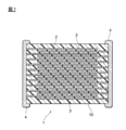
<1.積層セラミックコンデンサ>
本実施形態に係る電子部品の一例としての積層セラミックコンデンサ1が図1に示される。積層セラミックコンデンサ1は、誘電体層2と、内部電極層3と、が交互に積層された構成の素子本体10を有する。この素子本体10の両端部には、素子本体10の内部で交互に配置された内部電極層3と各々導通する一対の外部電極4が形成してある。素子本体10の形状に特に制限はないが、通常、直方体状とされる。また、素子本体10の寸法にも特に制限はなく、用途に応じて適当な寸法とすればよい。
< 1. Multilayer ceramic capacitor >
A multilayer ceramic capacitor 1 as an example of an electronic component according to this embodiment is shown in FIG. The multilayer ceramic capacitor 1 has an
1.1 誘電体層
誘電体層2は、後述する本実施形態に係る誘電体組成物から構成されている。
1.1 Dielectric Layer The
誘電体層2の1層あたりの厚み(層間厚み)は特に限定されず、所望の特性や用途等に応じて任意に設定することができる。通常は、層間厚みは30μm以下であることが好ましく、より好ましくは20μm以下であり、さらに好ましくは10μm以下である。
The thickness per layer (interlayer thickness) of the
なお、本実施形態では、誘電体組成物が後述するCa-Si-P-O偏析相16を有することにより、誘電体層2の厚みを薄くしても、高温多湿の環境下におけるクラック発生が抑制される。このため、本実施形態では、誘電体層2を2μmまで薄くすることができる。
In addition, in this embodiment, since the dielectric composition has the Ca-Si-P-O segregated
また、誘電体層2の積層数は特に限定されないが、本実施形態では、たとえば20以上であることが好ましい。
Further, the number of stacked
1.2 内部電極層
本実施形態では、内部電極層3は、各端部が素子本体10の対向する2端面の表面に交互に露出するように積層してある。
1.2 Internal Electrode Layer In this embodiment, the
内部電極層3に含有される導電材としては特に限定されない。導電材として用いられる貴金属としては、たとえばPd、Pt、Ag-Pd合金等が挙げられる。導電材として用いられる卑金属としては、たとえばNi、Ni系合金、Cu、Cu系合金等が挙げられる。なお、Ni、Ni系合金、CuまたはCu系合金中には、Pおよび/またはS等の各種微量成分が0.1質量%程度以下含まれていてもよい。また、内部電極層3は、市販の電極用ペーストを使用して形成してもよい。内部電極層3の厚さは用途等に応じて適宜決定すればよい。
The conductive material contained in the
1.3 外部電極
外部電極4に含有される導電材は特に限定されない。たとえばNi、Cu、Sn、Ag、Pd、Pt、Auあるいはこれらの合金、導電性樹脂等公知の導電材を用いればよい。外部電極4の厚さは用途等に応じて適宜決定すればよい。
1.3 External Electrode The conductive material contained in the
<2.誘電体組成物>
図2に示すように、本実施形態に係る誘電体層2を構成する誘電体組成物は、主相14の間にCa-Si-P-O偏析相16を含む。
< 2. Dielectric composition >
As shown in FIG. 2, the dielectric composition constituting the
2.1 主相
本実施形態の主相14はABO3で表される主成分を含む。なお、主相14の主成分とは、主相100質量部に対して、80~100質量部を占める成分であり、好ましくは、90~100質量部を占める成分である。
2.1 Main Phase The
(Aのモル比/Bのモル比)で表されるAとBとのモル比は1であってもよいし、1でなくてもよい。AとBのモル比は0.9~1.2であることが好ましい。 The molar ratio of A and B expressed as (molar ratio of A/molar ratio of B) may or may not be 1. The molar ratio of A and B is preferably 0.9 to 1.2.
Aはカルシウム(Ca)およびストロンチウム(Sr)から選ばれる少なくともいずれか1つを含む。本実施形態では、Aはカルシウム(Ca)であることが好ましい。 A contains at least one selected from calcium (Ca) and strontium (Sr). In this embodiment, A is preferably calcium (Ca).
また、Aとして含まれるカルシウム(Ca)およびストロンチウム(Sr)の合計を1モル部とした場合に、Aにはストロンチウム(Sr)が0~0.5モル部含まれていてもよい。 Further, when the total of calcium (Ca) and strontium (Sr) contained in A is 1 mole part, A may contain 0 to 0.5 mole part of strontium (Sr).
Bはジルコニウム(Zr)、チタン(Ti)、ハフニウム(Hf)およびマンガン(Mn)から選ばれる少なくともいずれか1つを含む。本実施形態では、Bはジルコニウム(Zr)であることが好ましい。 B contains at least one selected from zirconium (Zr), titanium (Ti), hafnium (Hf), and manganese (Mn). In this embodiment, B is preferably zirconium (Zr).
また、Bとして含まれるジルコニウム(Zr)、チタン(Ti)、ハフニウム(Hf)およびマンガン(Mn)の合計を1モル部とした場合に、Bには、チタン(Ti)が0~0.2モル部含まれることが好ましく、0~0.1モル部含まれることがより好ましい。 Furthermore, when the total of zirconium (Zr), titanium (Ti), hafnium (Hf), and manganese (Mn) contained in B is 1 mole part, B contains 0 to 0.2 parts of titanium (Ti). It is preferably contained in a molar part, and more preferably in a range of 0 to 0.1 molar part.
Bとして含まれるジルコニウム(Zr)、チタン(Ti)、ハフニウム(Hf)およびマンガン(Mn)の合計を1モル部とした場合に、Bには、ハフニウム(Hf)が0~0.05モル部含まれることが好ましく、0~0.02モル部含まれることがより好ましい。 When the total of zirconium (Zr), titanium (Ti), hafnium (Hf) and manganese (Mn) contained in B is 1 mole part, B contains 0 to 0.05 mole part of hafnium (Hf). It is preferably contained, and more preferably 0 to 0.02 mole part.
Bとして含まれるジルコニウム(Zr)、チタン(Ti)、ハフニウム(Hf)およびマンガン(Mn)の合計を1モル部とした場合に、Bには、マンガン(Mn)が0~0.05モル部含まれることが好ましく、0~0.03モル部含まれることがより好ましい。 When the total of zirconium (Zr), titanium (Ti), hafnium (Hf) and manganese (Mn) contained in B is 1 mole part, B contains 0 to 0.05 mole part of manganese (Mn). It is preferably contained, and more preferably 0 to 0.03 parts by mole.
本実施形態では、主相14は必要に応じて、アルミニウム(Al)、ケイ素(Si)、バナジウム(V)および希土類元素(RE)等の元素を含有してもよい。
In this embodiment, the
2.2 Ca-Si-P-O偏析相
図2に示すように、本実施形態に係る誘電体層2を構成する誘電体組成物は、上記の主相14の間に、Ca-Si-P-O偏析相16を含む。Ca-Si-P-O偏析相16には、少なくともカルシウム(Ca)、ケイ素(Si)およびリン(P)が含まれる。これにより、本実施形態の誘電体組成物は、高温多湿の環境下におけるクラックの発生に対して高い抑制効果を発揮することができる。
2.2 Ca-Si-P-O segregation phase As shown in Figure 2, the dielectric composition constituting the
Ca-Si-P-O偏析相16に含まれるカルシウム(Ca)、ストロンチウム(Sr)、ケイ素(Si)およびリン(P)の合計を1モル部としたとき、Ca-Si-P-O偏析相16には、カルシウム(Ca)が0.24~0.77モル部含まれることが好ましく、0.34~0.66モル部含まれることがより好ましい。
When the total of calcium (Ca), strontium (Sr), silicon (Si) and phosphorus (P) contained in the Ca-Si-
Ca-Si-P-O偏析相16に含まれるカルシウム(Ca)、ストロンチウム(Sr)、ケイ素(Si)およびリン(P)の合計を1モル部としたとき、Ca-Si-P-O偏析相16には、ストロンチウム(Sr)が0.00~0.40モル部含まれることが好ましく、0~0.3モル部含まれることがより好ましい。
When the total of calcium (Ca), strontium (Sr), silicon (Si) and phosphorus (P) contained in the Ca-Si-
Ca-Si-P-O偏析相16に含まれるカルシウム(Ca)、ストロンチウム(Sr)、ケイ素(Si)およびリン(P)の合計を1モル部としたとき、Ca-Si-P-O偏析相16には、ケイ素(Si)が0.05~0.30モル部含まれることが好ましく、0.07~0.25モル部含まれることがより好ましい。
When the total of calcium (Ca), strontium (Sr), silicon (Si) and phosphorus (P) contained in the Ca-Si-
Ca-Si-P-O偏析相16に含まれるカルシウム(Ca)、ストロンチウム(Sr)、ケイ素(Si)およびリン(P)の合計を1モル部としたとき、Ca-Si-P-O偏析相16には、リン(P)が0.05~0.40モル部含まれることが好ましく、0.05~0.30モル部含まれることがより好ましい。
When the total of calcium (Ca), strontium (Sr), silicon (Si) and phosphorus (P) contained in the Ca-Si-
なお、Ca-Si-P-O偏析相16は上記の元素以外の元素を含んでいてもよく、たとえばジルコニウム(Zr)、チタン(Ti)、ハフニウム(Hf)、マンガン(Mn)、マグネシウム(Mg)、ニオブ(Nb)、ホウ素(B)等の元素を含有してもよい。
Note that the Ca-Si-
Ca-Si-P-O偏析相16を構成する具体的な化合物としては、(Ca,Sr)5Si(PO6)2が好ましい。なお、ストロンチウム(Sr)は含まれなくても良い。
As a specific compound constituting the Ca-Si-P-O
本実施形態において、誘電体層2を構成する誘電体組成物がCa-Si-P-O偏析相16を有するか否かを判断する方法としては、特に限定されないが、以下に具体的な方法を例示する。
In the present embodiment, the method for determining whether or not the dielectric composition constituting the
まず、走査透過型電子顕微鏡(STEM)を用いて誘電体組成物の断面を撮影し、明視野(BF)像を得る。撮影する視野の広さは特に限定されないが、たとえば、1~10μm四方程度の広さである。この明視野像において主相14とは異なるコントラストを有する領域を異相であると認定する。異なるコントラストを有するか否か、すなわち異相を有するか否かの判断は、目視により行ってもよいし、画像処理を行うソフトウェア等により判断してもよい。
First, a cross section of the dielectric composition is photographed using a scanning transmission electron microscope (STEM) to obtain a bright field (BF) image. The width of the field of view to be photographed is not particularly limited, but is, for example, about 1 to 10 μm square. In this bright field image, a region having a contrast different from that of the
そして、上記の異相について、EDS分析により、カルシウム(Ca)、ケイ素(Si)およびリン(P)の各量を測定する。 Then, the amounts of calcium (Ca), silicon (Si), and phosphorus (P) in the above-mentioned different phase are measured by EDS analysis.
異相の同じ位置にカルシウム(Ca)、ケイ素(Si)およびリン(P)が存在している場合には、その異相はCa-Si-P-O偏析相16であると判断する。
If calcium (Ca), silicon (Si), and phosphorus (P) are present at the same position in a different phase, it is determined that the different phase is a Ca-Si-PO
この他にも、マッピング画像によりCa-Si-P-O偏析相16の有無を判断してもよい。具体的には、カルシウム(Ca)のマッピング画像と、ケイ素(Si)のマッピング画像と、リン(P)のマッピング画像と、を比較して、同じ位置にカルシウム(Ca)、ケイ素(Si)およびリン(P)が存在している箇所はCa-Si-P-O偏析相16であると判断する。
In addition to this, the presence or absence of the Ca-Si-P-O
本実施形態では、Ca-Si-P-O偏析相16の円相当径が0.02~1μmであることが好ましく、0.05~0.5μmであることがより好ましい。なお、円相当径とは、当該形状の面積と同じ面積を有する円の径を示す。
In this embodiment, the equivalent circle diameter of the Ca--Si--P--O segregated
本実施形態では、Ca-Si-P-O偏析相16の面積比率を「(Ca-Si-P-O偏析相の面積/主相の面積)×100[%]」の式で表す。
In this embodiment, the area ratio of the Ca-Si-P-O
本実施形態では、Ca-Si-P-O偏析相16の面積比率が0.5~10%であることが好ましく、1~5%であることがより好ましい。
In this embodiment, the area ratio of the Ca--Si--P--O segregated
本実施形態では、Ca-Si-P-O偏析相16の結晶系は斜方晶系であることが好ましい。
In this embodiment, the crystal system of the Ca--Si--P--O segregated
本実施形態では、誘電体組成物は、Ca-Zr-O系偏析相を含んでいてもよい。Ca-Zr-O系偏析相はCa安定化ジルコニアである。また、Ca-Zr-O系偏析相の結晶系は立方晶系である。 In this embodiment, the dielectric composition may include a Ca--Zr--O based segregated phase. The Ca-Zr-O segregated phase is Ca-stabilized zirconia. Further, the crystal system of the Ca--Zr--O segregated phase is a cubic system.
上記の通り、本実施形態の誘電体組成物の主相14はABO3で表される主成分を含み、Aはカルシウム(Ca)およびストロンチウム(Sr)から選ばれる少なくともいずれか1つであり、Bはジルコニウム(Zr)、チタン(Ti)、ハフニウム(Hf)およびマンガン(Mn)から選ばれる少なくともいずれか1つである。以下では、本実施形態の主相14の組成系を(Ca,Sr)ZrO3と表す。
As described above, the
主相14の組成系をBaTiO3とする場合に比べて、主相14の組成系を(Ca,Sr)ZrO3とすると、電圧を加えた際の静電容量の変化が小さく、温度を変えたときの静電容量の変化が小さく、高周波電流を流しても誘電損失が少ないために発熱が抑えられるというメリットがある。このため、主相14の組成系を(Ca,Sr)ZrO3とする誘電体組成物は、たとえば共振回路に好適に利用することもできる。
Compared to the case where the composition system of the
本発明者は、主相14の組成系を(Ca,Sr)ZrO3とする誘電体組成物がCa-Si-P-O偏析相16を有することにより、誘電体層2の厚みを薄くしても、高温多湿の環境下におけるコンデンサの抵抗劣化が抑制されることを見出した。その理由は必ずしも定かではないが、誘電体組成物に生じた軽度のクラックがCa-Si-P-O偏析相16に到達することにより、その軽度のクラックの進行が止まり、コンデンサの抵抗を低下させてしまう程度の大きなクラック発生が抑制されるためであると考えられる。
The present inventor has realized that the dielectric composition in which the composition system of the
このため、本実施形態では、誘電体層2の厚みを前述した厚みまで薄くすることができる。
Therefore, in this embodiment, the thickness of the
<3.積層セラミックコンデンサの製造方法>
次に、図1に示す積層セラミックコンデンサ1の製造方法の一例について以下に説明する。
< 3. Manufacturing method of multilayer ceramic capacitor >
Next, an example of a method for manufacturing the multilayer ceramic capacitor 1 shown in FIG. 1 will be described below.
本実施形態では、上記の誘電体組成物を構成する主相14の主成分であるABO3粒子の仮焼き粉末と、第1添加剤の仮焼き粉末と、第2添加剤の仮焼き粉末と、を用意する。
In this embodiment, a calcined powder of three ABO particles which is the main component of the
第1添加剤の仮焼き粉末とは、焼成後にCa-Si-P-O偏析相16を構成するカルシウム(Ca)、ストロンチウム(Sr)、ケイ素(Si)およびリン(P)の仮焼き粉末である。
The calcined powder of the first additive is a calcined powder of calcium (Ca), strontium (Sr), silicon (Si), and phosphorus (P) that constitutes the Ca-Si-
また、第2添加剤とは、焼成後にCa-Zr-O偏析相に含まれることになるカルシウム(Ca)およびジルコニウム(Zr)の仮焼き粉末である。 Further, the second additive is a calcined powder of calcium (Ca) and zirconium (Zr) that will be included in the Ca--Zr--O segregated phase after firing.
上記の各元素の原料としては特に限定されず、各元素の酸化物を用いることができる。また、焼成により各元素の酸化物を得ることができる各種化合物を用いることができる。リン(P)を除く各元素の各種化合物としては、たとえば炭酸塩、シュウ酸塩、硝酸塩、水酸化物、有機金属化合物等が例示される。本実施形態では、上記のリン(P)を除く各元素の出発原料は粉末であることが好ましい。リン(P)は様々な形態で添加できるが、たとえばリン酸系化合物等が例示される。 The raw materials for each of the above elements are not particularly limited, and oxides of each element can be used. Moreover, various compounds that can obtain oxides of each element by firing can be used. Examples of various compounds of each element except phosphorus (P) include carbonates, oxalates, nitrates, hydroxides, organometallic compounds, and the like. In this embodiment, it is preferable that the starting materials for each element except for phosphorus (P) are powders. Phosphorus (P) can be added in various forms, such as phosphoric acid compounds.
準備した出発原料のうち、ABO3粒子の原料を所定の割合に秤量した後、ボールミル等を用いて所定の時間、湿式混合を行う。混合粉を乾燥後、大気中において700~1300℃の範囲で熱処理を行い、ABO3粒子の仮焼き粉末を得る。また、仮焼き粉末はボールミル等を用いて所定の時間、粉砕を行ってもよい。 Among the prepared starting materials, the raw materials for 3 ABO particles are weighed in a predetermined ratio, and then wet-mixed for a predetermined time using a ball mill or the like. After drying the mixed powder, heat treatment is performed in the air at a temperature of 700 to 1300°C to obtain a calcined powder of 3 ABO particles. Further, the calcined powder may be pulverized for a predetermined period of time using a ball mill or the like.
焼成後にCa-Si-P-O偏析相16を構成するカルシウム(Ca)、ストロンチウム(Sr)、およびケイ素(Si)の酸化物等の各種化合物等ならびにリン(P)酸系化合物等の各種化合物等を準備し、熱処理して第1添加剤の仮焼き粉末を得る。
Various compounds such as oxides of calcium (Ca), strontium (Sr), and silicon (Si), and various compounds such as phosphoric (P) acid-based compounds, which constitute the Ca-Si-P-O
第1添加剤の仮焼き粉末の粉砕条件を変えることで、Ca-Si-P-O偏析相16の円相当径を変えることができる。たとえばボールミルの粉砕時間を変えることで円相当径を調整することができる。
By changing the grinding conditions of the calcined powder of the first additive, the equivalent circle diameter of the Ca--Si--P--O segregated
焼成後にCa-Zr-O系偏析相を構成するカルシウム(Ca)およびジルコニウム(Zr)の酸化物等の各種化合物等を準備し、熱処理して第2添加剤の仮焼き粉末を得る。 Various compounds such as oxides of calcium (Ca) and zirconium (Zr) that constitute the Ca--Zr--O segregated phase after firing are prepared and heat-treated to obtain a calcined powder of the second additive.
続いて、グリーンチップを作製するためのペーストを調製する。得られたABO3粒子の仮焼き粉末と、第1添加剤の仮焼き粉末と、第2添加剤の仮焼き粉末と、バインダと、溶剤と、を混練し塗料化して誘電体層用ペーストを調製する。バインダおよび溶剤は、公知のものを用いればよい。 Next, a paste for producing green chips is prepared. The obtained calcined powder of ABO 3 particles, the calcined powder of the first additive, the calcined powder of the second additive, a binder, and a solvent are kneaded and made into a paint to form a dielectric layer paste. Prepare. Known binders and solvents may be used.
誘電体層用ペーストは、必要に応じて、可塑剤や分散剤等の添加物を含んでもよい。 The dielectric layer paste may contain additives such as a plasticizer and a dispersant, if necessary.
内部電極層用ペーストは、上述した導電材の原料と、バインダと、溶剤と、を混練して得られる。バインダおよび溶剤は、公知のものを用いればよい。内部電極層用ペーストは、必要に応じて、共材や可塑剤等の添加物を含んでもよい。 The internal electrode layer paste is obtained by kneading the above-mentioned conductive material raw material, binder, and solvent. Known binders and solvents may be used. The internal electrode layer paste may contain additives such as co-materials and plasticizers, if necessary.
外部電極用ペーストは、内部電極層用ペーストと同様にして調製することができる。 The paste for external electrodes can be prepared in the same manner as the paste for internal electrode layers.
得られた各ペーストを用いて、グリーンシートおよび内部電極パターンを形成し、これらを積層してグリーンチップを得る。 Using each of the obtained pastes, a green sheet and an internal electrode pattern are formed, and these are laminated to obtain a green chip.
得られたグリーンチップに対し、必要に応じて、脱バインダ処理を行う。脱バインダ処理条件は、たとえば、保持温度を好ましくは200~350℃とする。 The obtained green chips are subjected to binder removal treatment, if necessary. As for the binder removal treatment conditions, for example, the holding temperature is preferably 200 to 350°C.
脱バインダ処理後、グリーンチップの焼成を行い、素子本体10を得る。本実施形態では、焼成時の雰囲気は特に限定されず、空気中であってもよいし、還元雰囲気下であってもよい。本実施形態では、焼成時の保持温度は特に限定されず、たとえば1200~1350℃である。
After the binder removal process, the green chip is fired to obtain the
焼成後、得られた素子本体10に対し、必要に応じて、再酸化処理(アニール)を行う。アニール条件は、たとえば、アニール時の酸素分圧を焼成時の酸素分圧よりも高い酸素分圧とし、保持温度を1150℃以下とすることが好ましい。
After firing, the obtained
上記のようにして得られた素子本体10の誘電体層2を構成する誘電体組成物は、上述した誘電体組成物である。この素子本体10に端面研磨を施し、外部電極用ペーストを塗布して焼き付けし、外部電極4を形成する。そして、必要に応じて、外部電極4の表面に、めっき等により被覆層を形成する。
The dielectric composition constituting the
このようにして、本実施形態に係る積層セラミックコンデンサ1が製造される。 In this way, the multilayer ceramic capacitor 1 according to this embodiment is manufactured.
[変形例]
上述した実施形態では、本発明に係る電子部品が積層セラミックコンデンサである場合について説明したが、本発明に係る電子部品は、積層セラミックコンデンサに限定されず、上述した誘電体組成物を有する電子部品であれば何でもよい。
[ Modified example ]
In the embodiments described above, the electronic component according to the present invention is a multilayer ceramic capacitor, but the electronic component according to the present invention is not limited to a multilayer ceramic capacitor, but can also be an electronic component having the dielectric composition described above. Anything is fine.
たとえば、上述した誘電体組成物に一対の電極が形成された単板型のセラミックコンデンサであってもよい。 For example, it may be a single-plate ceramic capacitor in which a pair of electrodes are formed on the dielectric composition described above.
また、誘電体組成物には、Ca-Zr-O系偏析相が含まれていなくてもよい。 Furthermore, the dielectric composition does not need to contain a Ca--Zr--O segregated phase.
以上、本発明の実施形態について説明してきたが、本発明は上記の実施形態に何ら限定されるものではなく、本発明の範囲内において種々の態様で改変してもよい。 Although the embodiments of the present invention have been described above, the present invention is not limited to the above-described embodiments, and may be modified in various ways within the scope of the present invention.
以下、実施例および比較例を用いて、本発明をさらに詳細に説明する。ただし、本発明は以下の実施例に限定されるものではない。 Hereinafter, the present invention will be explained in more detail using Examples and Comparative Examples. However, the present invention is not limited to the following examples.
<実験1>
試料番号1~25では、誘電体組成物に含まれる主相の出発原料として、炭酸カルシウム(CaCO3)、炭酸ストロンチウム(SrCO3)、酸化ジルコニウム(ZrO2)、酸化チタン(TiO2)、酸化ハフニウム(HfO2)および炭酸マンガン(MnCO3)の粉末を準備した。焼成後の主相の組成が表1に記載の通りになるように、準備した出発原料を秤量した。
<Experiment 1>
In sample numbers 1 to 25, the starting materials for the main phase contained in the dielectric composition were calcium carbonate (CaCO 3 ), strontium carbonate (SrCO 3 ), zirconium oxide (ZrO 2 ), titanium oxide (TiO 2 ), and oxide. Hafnium (HfO 2 ) and manganese carbonate (MnCO 3 ) powders were prepared. The prepared starting materials were weighed so that the composition of the main phase after firing was as shown in Table 1.
次に、秤量した各粉末を、分散媒としてのイオン交換水を用いてボールミルにより16時間湿式混合し、混合物を乾燥して混合原料粉末を得た。その後、得られた混合原料粉末を、大気中において保持温度900℃、保持時間2時間の条件で熱処理を行い、主相の主成分化合物の仮焼き粉末を得た。 Next, the weighed powders were wet mixed for 16 hours in a ball mill using ion-exchanged water as a dispersion medium, and the mixture was dried to obtain a mixed raw material powder. Thereafter, the obtained mixed raw material powder was heat treated in the atmosphere at a holding temperature of 900° C. and a holding time of 2 hours to obtain a calcined powder of the main component compound of the main phase.
また、第1添加剤の原料として、炭酸カルシウム(CaCO3)、炭酸ストロンチウム(SrCO3)、酸化ケイ素(SiO2)およびリン酸二水素アンモニウム(NH4H2PO4)の粉末を準備した。第1添加剤を構成する各元素のモル比が表1に記載の通りとなり、なおかつ、第1添加剤の添加量が3質量部となるように、準備した出発原料を秤量した。 In addition, powders of calcium carbonate (CaCO 3 ), strontium carbonate (SrCO 3 ), silicon oxide (SiO 2 ), and ammonium dihydrogen phosphate (NH 4 H 2 PO 4 ) were prepared as raw materials for the first additive. The prepared starting materials were weighed so that the molar ratio of each element constituting the first additive was as shown in Table 1, and the amount of the first additive added was 3 parts by mass.
なお、第1添加剤の添加量とは、主相の主成分を100質量部としたときの第1添加剤の添加量である。 Note that the amount of the first additive added is the amount of the first additive added when the main component of the main phase is 100 parts by mass.
炭酸カルシウム(CaCO3)、炭酸ストロンチウム(SrCO3)、酸化ケイ素(SiO2)およびリン酸二水素アンモニウム(NH4H2PO4)の粉末に対して、大気中において保持温度900℃、保持時間2時間の条件で熱処理を行い、第1添加剤の仮焼き粉末を得た。 Powders of calcium carbonate (CaCO 3 ), strontium carbonate (SrCO 3 ), silicon oxide (SiO 2 ), and ammonium dihydrogen phosphate (NH 4 H 2 PO 4 ) were heated at a holding temperature of 900°C and a holding time in the atmosphere. Heat treatment was performed for 2 hours to obtain a calcined powder of the first additive.
得られた主相の主成分化合物の仮焼き粉末および第1添加剤の仮焼き粉末を分散媒としてのイオン交換水を用いてボールミルにより16時間湿式粉砕し、乾燥し、誘電体原料を得た。 The obtained calcined powder of the main component compound of the main phase and the calcined powder of the first additive were wet-pulverized for 16 hours in a ball mill using ion-exchanged water as a dispersion medium, and dried to obtain a dielectric raw material. .
得られた誘電体原料:100質量部と、ポリビニルブチラール樹脂:10質量部と、可塑剤としてのジオクチルフタレート(DOP):5質量部と、溶媒としてのメチルエチルケトン(MEK):100質量部とをボールミルで混合してペースト化し、誘電体層用ペーストを得た。 100 parts by mass of the obtained dielectric raw material, 10 parts by mass of polyvinyl butyral resin, 5 parts by mass of dioctyl phthalate (DOP) as a plasticizer, and 100 parts by mass of methyl ethyl ketone (MEK) as a solvent were milled in a ball mill. The mixture was mixed to form a paste to obtain a dielectric layer paste.
また、Ni粒子:44.6質量部と、テルピネオール:52質量部と、エチルセルロース:3質量部と、ベンゾトリアゾール:0.4質量部とを、3本ロールにより混練し、ペースト化して内部電極層用ペーストを作製した。 In addition, 44.6 parts by mass of Ni particles, 52 parts by mass of terpineol, 3 parts by mass of ethyl cellulose, and 0.4 parts by mass of benzotriazole were kneaded using three rolls and made into a paste to form an internal electrode layer. A paste was prepared.
そして、上記にて作製した誘電体層用ペーストを用いて、PETフィルム上に、グリーンシートを形成した。次いで、この上に内部電極層用ペーストを用いて、内部電極層を所定パターンで印刷した後、PETフィルムからシートを剥離し、内部電極層を有するグリーンシートを作製した。 Then, a green sheet was formed on the PET film using the dielectric layer paste prepared above. Next, an internal electrode layer was printed on this in a predetermined pattern using an internal electrode layer paste, and then the sheet was peeled off from the PET film to produce a green sheet having an internal electrode layer.
次いで、内部電極層を有するグリーンシートを複数枚積層し、加圧接着することによりグリーン積層体とし、このグリーン積層体を所定サイズに切断することにより、グリーンチップを得た。 Next, a plurality of green sheets having internal electrode layers were laminated and bonded under pressure to form a green laminate, and this green laminate was cut into a predetermined size to obtain a green chip.
次いで、得られたグリーンチップについて、脱バインダ処理、焼成およびアニールを下記条件にて行って、素子本体を得た。 Next, the obtained green chip was subjected to binder removal treatment, firing, and annealing under the following conditions to obtain an element body.
脱バインダ処理条件は、昇温速度:25℃/時間、保持温度:260℃、温度保持時間:8時間、雰囲気:空気中とした。 The binder removal treatment conditions were: temperature increase rate: 25° C./hour, holding temperature: 260° C., temperature holding time: 8 hours, and atmosphere: in air.
焼成条件は、昇温速度:200℃/時間、保持温度:1200℃とし、保持時間を2時間とした。降温速度は200℃/時間とした。なお、雰囲気ガスは、加湿したN2+H2混合ガスとし、酸素分圧が10-12MPaとなるようにした。 The firing conditions were a temperature increase rate of 200° C./hour, a holding temperature of 1200° C., and a holding time of 2 hours. The temperature decreasing rate was 200°C/hour. Note that the atmospheric gas was a humidified N 2 +H 2 mixed gas, and the oxygen partial pressure was set to 10 −12 MPa.
アニール条件は、昇温速度:200℃/時間、保持温度:1000℃、温度保持時間:2時間、降温速度:200℃/時間、雰囲気ガス:加湿したN2ガス(酸素分圧:10-7MPa)とした。 The annealing conditions were: temperature increase rate: 200°C/hour, holding temperature: 1000°C, temperature holding time: 2 hours, temperature decreasing rate: 200°C/hour, atmosphere gas: humidified N 2 gas (oxygen partial pressure: 10 -7 MPa).
なお、焼成およびアニールの際の雰囲気ガスの加湿には、ウェッターを用いた。 Note that a wetter was used to humidify the atmospheric gas during firing and annealing.
次いで、得られたコンデンサ素子本体の表面をバレル研磨した。その後、外部電極としてCuを塗布した後に窒素ガス中で焼付を行い、図1に示す積層セラミックコンデンサのコンデンサ試料を得た。得られたコンデンサ試料のサイズは、3.2mm×1.6mm×1.6mmであり、誘電体層の厚み2.5μm、内部電極層の厚み1.1μm、内部電極層に挟まれた内層誘電体層の数は200とした。 Next, the surface of the obtained capacitor element body was barrel polished. Thereafter, Cu was applied as an external electrode and baked in nitrogen gas to obtain a capacitor sample of the multilayer ceramic capacitor shown in FIG. 1. The size of the obtained capacitor sample was 3.2 mm x 1.6 mm x 1.6 mm, with a dielectric layer thickness of 2.5 μm, an internal electrode layer thickness of 1.1 μm, and an inner dielectric layer sandwiched between the internal electrode layers. The number of body layers was 200.
得られたコンデンサ試料の誘電体組成物(誘電体層)の断面の10μm×10μmの視野について、STEMにより異相を認定し、EDSを用いて、カルシウム(Ca)、ストロンチウム(Sr)、ケイ素(Si)およびリン(P)の各量を測定して、Ca-Si-P-O偏析相であるか否かの判断をした。 With respect to a 10 μm x 10 μm field of view of the cross section of the dielectric composition (dielectric layer) of the obtained capacitor sample, different phases were identified using STEM, and calcium (Ca), strontium (Sr), and silicon (Si) were identified using EDS. ) and phosphorus (P) to determine whether the phase was a Ca-Si-P-O segregated phase or not.
なお、表1の各コンデンサ試料では、カルシウム(Ca)、ストロンチウム(Sr)、ケイ素(Si)およびリン(P)の第1添加剤のモル比とCa-Si-P-O偏析相の平均のモル比は一致していた。 In addition, in each capacitor sample in Table 1, the molar ratio of the first additive of calcium (Ca), strontium (Sr), silicon (Si), and phosphorus (P) and the average of the Ca-Si-P-O segregated phase are The molar ratios were consistent.
得られた誘電体組成物(誘電体層)に含まれていたCa-Si-P-O偏析相について、電子線回折を行い、電子線回折図形を分析することで結晶系を解析した。結果を表1に示す。 Electron diffraction was performed on the Ca-Si-P-O segregated phase contained in the obtained dielectric composition (dielectric layer), and the crystal system was analyzed by analyzing the electron diffraction pattern. The results are shown in Table 1.
第1PCBT試験は以下の通り行った。コンデンサ試料をFR4基板(ガラスエポキシ基板)にSn-Ag-Cu半田で実装し、プレッシャークッカー槽に投入し、121℃、湿度95%の雰囲気下で50Vの電圧印加を100時間行う加速耐湿負荷試験を実施した。各コンデンサ試料について、500個ずつ試験を実施した。各コンデンサ試料の不良数を表1に示す。 The first PCBT test was conducted as follows. Accelerated humidity load test in which a capacitor sample is mounted on an FR4 board (glass epoxy board) with Sn-Ag-Cu solder, placed in a pressure cooker tank, and a voltage of 50V is applied for 100 hours in an atmosphere of 121°C and 95% humidity. was carried out. A test was conducted on 500 capacitor samples of each capacitor sample. Table 1 shows the number of defects for each capacitor sample.

<実験2>
試料番号31では、主相の主成分化合物の仮焼き粉末および第1添加剤の仮焼き粉末の他に第2添加剤の仮焼き粉末を加えて、分散媒を用いてボールミルにより粉砕し、乾燥し、誘電体原料を得た以外は、実験1と同様にしてコンデンサ試料を得た。なお、第2添加剤は焼成後にCa-Zr-O偏析相となる成分である。
<
In sample No. 31, in addition to the calcined powder of the main component compound of the main phase and the calcined powder of the first additive, the calcined powder of the second additive was added, crushed in a ball mill using a dispersion medium, and dried. A capacitor sample was obtained in the same manner as in Experiment 1 except that the dielectric raw material was obtained. Note that the second additive is a component that becomes a Ca--Zr--O segregated phase after firing.
なお、第2添加剤の原料として、炭酸カルシウム(CaCO3)および酸化ジルコニウム(ZrO2)の粉末を準備した。第2添加剤において、Ca元素とZr元素はモル比でCa:Zr=0.15:0.85であった。第2添加剤の添加量は、1質量部であった。 Note that powders of calcium carbonate (CaCO 3 ) and zirconium oxide (ZrO 2 ) were prepared as raw materials for the second additive. In the second additive, the molar ratio of Ca element and Zr element was Ca:Zr=0.15:0.85. The amount of the second additive added was 1 part by mass.
試料番号31では、実験1と同様にして、Ca-Si-P-O偏析相の存在を確認した。 In sample number 31, the presence of a Ca-Si-P-O segregated phase was confirmed in the same manner as in Experiment 1.
試料番号31では、以下の方法により、Ca-Zr-O偏析相の存在を判断した。得られたコンデンサ試料の誘電体組成物(誘電体層)の断面の10μm×10μmの視野について、STEMにより異相を認定し、EDSを用いて、同じ位置にカルシウム(Ca)およびジルコニウム(Zr)が存在しており、なおかつ、Ca-Si-P-O偏析相ではない異相をCa-Zr-O偏析相であると判断することとした。試料番号31では、Ca-Zr-O偏析相の存在を確認した。 In sample number 31, the presence of a Ca--Zr--O segregated phase was determined by the following method. With respect to a field of view of 10 μm x 10 μm in cross section of the dielectric composition (dielectric layer) of the obtained capacitor sample, a different phase was identified using STEM, and calcium (Ca) and zirconium (Zr) were detected at the same position using EDS. A heterogeneous phase that is present and is not a Ca-Si-P-O segregated phase is determined to be a Ca-Zr-O segregated phase. In sample number 31, the presence of a Ca-Zr-O segregated phase was confirmed.
試料番号31では、実験1と同様にして、第1PCBT試験を実施した。結果を表2に示す。 For sample number 31, the first PCBT test was conducted in the same manner as in Experiment 1. The results are shown in Table 2.

表2より、Ca-Si-P-O偏析相の他に、Ca-Zr-O偏析相を有する場合(試料番号31)も、第1PCBT試験による不良数が少なく、高温多湿の環境下におけるクラックの発生に対して高い抑制効果を発揮することが確認できた。 From Table 2, in addition to the Ca-Si-P-O segregated phase, the case with the Ca-Zr-O segregated phase (sample number 31) also showed a small number of defects in the first PCBT test, and cracks in a high temperature and humid environment. It was confirmed that this method has a high suppressive effect on the occurrence of.
<実験3>
試料番号41~44では、第1添加剤の仮焼き粉末のボールミルでの粉砕時間を変えることで円相当径を調整した以外は、実験1と同様にしてコンデンサ試料を得た。
<
For sample numbers 41 to 44, capacitor samples were obtained in the same manner as in Experiment 1, except that the equivalent circle diameter was adjusted by changing the milling time of the calcined powder of the first additive in a ball mill.
試料番号41~44では、実験1と同様にして、Ca-Si-P-O偏析相の存在を判断した。結果を表3に示す。 For sample numbers 41 to 44, the presence of a Ca-Si-P-O segregated phase was determined in the same manner as in Experiment 1. The results are shown in Table 3.
試料番号2、41~44では、10箇所の10μm四方の視野におけるCa-Si-P-O偏析相の平均の円相当径を求めた。
For
試料番号41~44では、実験1と同様にして、第1PCBT試験を実施した。結果を表3に示す。 For sample numbers 41 to 44, the first PCBT test was conducted in the same manner as in Experiment 1. The results are shown in Table 3.
第2PCBT試験は以下の通り行った。コンデンサ試料をFR4基板(ガラスエポキシ基板) にSn-Ag-Cu半田で実装し、プレッシャークッカー槽に投入し、121℃、湿度95%の雰囲気下で50Vの電圧印加を500時間行う加速耐湿負荷試験を実施した。各コンデンサ試料について、100個ずつ試験を実施した。各コンデンサ試料の不良数を表3に示す。 The second PCBT test was conducted as follows. Accelerated humidity load test in which a capacitor sample was mounted on an FR4 board (glass epoxy board) with Sn-Ag-Cu solder, placed in a pressure cooker tank, and a voltage of 50V was applied for 500 hours in an atmosphere of 121°C and 95% humidity. was carried out. A test was conducted on 100 capacitor samples of each capacitor sample. Table 3 shows the number of defects for each capacitor sample.

表3より、Ca-Si-P-O偏析相の円相当径が0.02μmより大きく、1μm未満の場合(試料番号42、2および43)は、Ca-Si-P-O偏析相の円相当径が0.02μmの場合(試料番号41)およびCa-Si-P-O偏析相の円相当径が1μmの場合(試料番号44)に比べて、第2PCBT試験による不良数が少なく、高温多湿の環境下におけるクラックの発生に対してより高い抑制効果を発揮することが確認できた。
From Table 3, when the equivalent circle diameter of the Ca-Si-P-O segregated phase is larger than 0.02 μm and less than 1 μm (
<実験4>
試料番号51~54では、第1添加剤の添加量を変化させた以外は、実験1と同様にしてコンデンサ試料を得た。
<
For sample numbers 51 to 54, capacitor samples were obtained in the same manner as in Experiment 1, except that the amount of the first additive added was changed.
試料番号51~54では、実験1と同様にして、Ca-Si-P-O偏析相の存在を判断した。 For sample numbers 51 to 54, the presence of a Ca-Si-P-O segregated phase was determined in the same manner as in Experiment 1.
試料番号2、51~54では、10箇所の10μm四方の視野におけるCa-Si-P-O偏析相の平均の面積比率を求めた。
For
試料番号51~54では、実験1と同様にして、第1PCBT試験を実施した。結果を表4に示す。 For sample numbers 51 to 54, the first PCBT test was conducted in the same manner as in Experiment 1. The results are shown in Table 4.
試料番号51~54では、実験3と同様にして、第2PCBT試験を実施した。結果を表4に示す。
For sample numbers 51 to 54, a second PCBT test was conducted in the same manner as in

表4より、Ca-Si-P-O偏析相の面積比率が0.5より大きく、10未満の場合(試料番号52、2および53)は、Ca-Si-P-O偏析相の面積比率が0.5の場合(試料番号51)およびCa-Si-P-O偏析相の面積比率が10の場合(試料番号54)に比べて、第2PCBT試験による不良数が少なく、高温多湿の環境下におけるクラックの発生に対してより高い抑制効果を発揮することが確認できた。
From Table 4, when the area ratio of the Ca-Si-P-O segregated phase is greater than 0.5 and less than 10 (
1… 積層セラミックコンデンサ
10… 素子本体
2… 誘電体層
14… 主相
16… Ca-Si-P-O偏析相
3… 内部電極層
4… 外部電極
1... Multilayer
Claims (8)
前記主相はABO3で表される主成分を含み、
前記Aはカルシウムを少なくとも含み、前記Bはジルコニウムを少なくとも含み、
前記Ca-Si-P-O結晶相には、少なくともカルシウム、ケイ素およびリンが含まれる誘電体組成物であって、
前記Ca-Si-P-O結晶相に含まれるカルシウム、ストロンチウム、ケイ素およびリンの合計を1モル部としたとき、
前記Ca-Si-P-O結晶相には、
ケイ素が0.05モル部以上含まれ、
リンが0.05モル部以上含まれる誘電体組成物。 A dielectric composition comprising a main phase and a Ca-Si-P- O crystal phase ,
The main phase includes a main component represented by ABO3 ,
The A contains at least calcium , the B contains at least zirconium ,
The Ca-Si-P- O crystal phase contains at least calcium, silicon, and phosphorus, the dielectric composition comprising:
When the total of calcium, strontium, silicon and phosphorus contained in the Ca-Si-P-O crystal phase is 1 mole part,
The Ca-Si-P-O crystal phase includes:
Contains 0.05 mole part or more of silicon,
A dielectric composition containing 0.05 mole part or more of phosphorus .
前記Ca-Si-P-O結晶相には、
カルシウムが0.24~0.77モル部含まれ、
ストロンチウムが0.00~0.40モル部含まれ、
ケイ素が0.05~0.30モル部含まれ、
リンが0.05~0.40モル部含まれる請求項1に記載の誘電体組成物。 When the total of calcium, strontium, silicon and phosphorus contained in the Ca-Si-P- O crystal phase is 1 mole part,
The Ca-Si-P- O crystal phase includes:
Contains 0.24 to 0.77 mole part of calcium,
Contains 0.00 to 0.40 mole part of strontium,
Contains 0.05 to 0.30 mole part of silicon,
The dielectric composition according to claim 1, containing 0.05 to 0.40 parts by mole of phosphorus.
Priority Applications (3)
| Application Number | Priority Date | Filing Date | Title |
|---|---|---|---|
| JP2019224821A JP7351205B2 (en) | 2019-12-12 | 2019-12-12 | Dielectric compositions and electronic components |
| US17/115,100 US11472742B2 (en) | 2019-12-12 | 2020-12-08 | Dielectric composition and electronic component |
| CN202011448458.5A CN112979308B (en) | 2019-12-12 | 2020-12-11 | Dielectric composition and electronic component |
Applications Claiming Priority (1)
| Application Number | Priority Date | Filing Date | Title |
|---|---|---|---|
| JP2019224821A JP7351205B2 (en) | 2019-12-12 | 2019-12-12 | Dielectric compositions and electronic components |
Publications (2)
| Publication Number | Publication Date |
|---|---|
| JP2021091586A JP2021091586A (en) | 2021-06-17 |
| JP7351205B2 true JP7351205B2 (en) | 2023-09-27 |
Family
ID=76312185
Family Applications (1)
| Application Number | Title | Priority Date | Filing Date |
|---|---|---|---|
| JP2019224821A Active JP7351205B2 (en) | 2019-12-12 | 2019-12-12 | Dielectric compositions and electronic components |
Country Status (3)
| Country | Link |
|---|---|
| US (1) | US11472742B2 (en) |
| JP (1) | JP7351205B2 (en) |
| CN (1) | CN112979308B (en) |
Families Citing this family (4)
| Publication number | Priority date | Publication date | Assignee | Title |
|---|---|---|---|---|
| KR102691312B1 (en) * | 2018-09-05 | 2024-08-05 | 삼성전기주식회사 | Multilayer ceramic electronic component |
| JP2020155523A (en) * | 2019-03-19 | 2020-09-24 | 株式会社村田製作所 | Multilayer ceramic capacitor |
| JP7306251B2 (en) * | 2019-12-12 | 2023-07-11 | Tdk株式会社 | Dielectric compositions and electronic components |
| JP7276663B2 (en) * | 2019-12-27 | 2023-05-18 | Tdk株式会社 | Dielectric compositions and electronic components |
Citations (2)
| Publication number | Priority date | Publication date | Assignee | Title |
|---|---|---|---|---|
| CN104310985A (en) | 2014-10-16 | 2015-01-28 | 桂林理工大学 | Ultra-low dielectric constant microwave dielectric ceramic Ca2PO4F and its preparation method |
| JP2015189592A (en) | 2014-03-27 | 2015-11-02 | 新日鐵住金株式会社 | Raw material for phosphate fertilizer and production method thereof |
Family Cites Families (12)
| Publication number | Priority date | Publication date | Assignee | Title |
|---|---|---|---|---|
| JP3207847B2 (en) * | 1989-10-18 | 2001-09-10 | ティーディーケイ株式会社 | Multilayer ceramic chip capacitors |
| JP2001307940A (en) | 2000-04-26 | 2001-11-02 | Taiyo Yuden Co Ltd | Laminated ceramic capacitor and its manufacturing method |
| JP2002265261A (en) | 2001-03-07 | 2002-09-18 | Murata Mfg Co Ltd | Laminated ceramic capacitor |
| JP4480367B2 (en) * | 2002-08-27 | 2010-06-16 | 京セラ株式会社 | Dielectric porcelain and its manufacturing method, and multilayer electronic component and its manufacturing method |
| JP4614656B2 (en) * | 2003-12-24 | 2011-01-19 | 京セラ株式会社 | Dielectric porcelain, multilayer electronic component, and method of manufacturing multilayer electronic component |
| JP4299759B2 (en) * | 2004-10-12 | 2009-07-22 | Tdk株式会社 | Ceramic electronic component and manufacturing method thereof |
| JP5152017B2 (en) * | 2009-01-30 | 2013-02-27 | 株式会社村田製作所 | Dielectric ceramic and multilayer ceramic capacitors |
| JP5040971B2 (en) | 2009-08-12 | 2012-10-03 | 株式会社村田製作所 | Dielectric ceramic, manufacturing method thereof, and multilayer ceramic capacitor |
| US8906818B2 (en) * | 2009-10-13 | 2014-12-09 | Recapping, Inc. | High energy density ionic dielectric materials and devices |
| JP5224074B2 (en) * | 2010-08-04 | 2013-07-03 | 株式会社村田製作所 | Dielectric ceramic and multilayer ceramic capacitor |
| CN103443050B (en) * | 2011-03-16 | 2016-09-28 | 株式会社村田制作所 | Dielectric ceramics and laminated ceramic capacitor |
| JP6213337B2 (en) * | 2014-03-26 | 2017-10-18 | Tdk株式会社 | Dielectric porcelain composition and electronic component |
-
2019
- 2019-12-12 JP JP2019224821A patent/JP7351205B2/en active Active
-
2020
- 2020-12-08 US US17/115,100 patent/US11472742B2/en active Active
- 2020-12-11 CN CN202011448458.5A patent/CN112979308B/en active Active
Patent Citations (2)
| Publication number | Priority date | Publication date | Assignee | Title |
|---|---|---|---|---|
| JP2015189592A (en) | 2014-03-27 | 2015-11-02 | 新日鐵住金株式会社 | Raw material for phosphate fertilizer and production method thereof |
| CN104310985A (en) | 2014-10-16 | 2015-01-28 | 桂林理工大学 | Ultra-low dielectric constant microwave dielectric ceramic Ca2PO4F and its preparation method |
Non-Patent Citations (1)
| Title |
|---|
| ZHANG M et al.,New insight into the crystal structure of Sr4Ca(PO4)SiO4 and the photoluminescence tuning of Sr4Ca(PO4)2SiO4:Ce3+,Na+,Eu2+ phostors,journal of materials chemistry C,vol.2016 No.4,P.9078-9084,doi:10.1039/c6tc03373c |
Also Published As
| Publication number | Publication date |
|---|---|
| JP2021091586A (en) | 2021-06-17 |
| CN112979308A (en) | 2021-06-18 |
| CN112979308B (en) | 2024-04-02 |
| US20210179494A1 (en) | 2021-06-17 |
| US11472742B2 (en) | 2022-10-18 |
Similar Documents
| Publication | Publication Date | Title |
|---|---|---|
| JP6213337B2 (en) | Dielectric porcelain composition and electronic component | |
| JP5217405B2 (en) | Dielectric porcelain composition and electronic component | |
| JP5360079B2 (en) | Dielectric ceramic composition and ceramic electronic component | |
| JP7351205B2 (en) | Dielectric compositions and electronic components | |
| JP5434407B2 (en) | Ceramic electronic component and manufacturing method thereof | |
| JP5018604B2 (en) | Dielectric porcelain composition and electronic component | |
| JP5034839B2 (en) | Dielectric porcelain composition and electronic component | |
| CN107793148B (en) | Dielectric composition and laminated electronic component | |
| JP7306251B2 (en) | Dielectric compositions and electronic components | |
| JP6089770B2 (en) | Dielectric porcelain composition and electronic component | |
| JP2012072037A (en) | Dielectric ceramic composition, method for producing the same and ceramic electronic part | |
| JP2017120856A (en) | Ceramic electronic component | |
| JP4863005B2 (en) | Dielectric porcelain composition and electronic component | |
| JP5482747B2 (en) | Dielectric ceramic composition and ceramic electronic component | |
| JP5803694B2 (en) | Dielectric ceramic composition and ceramic electronic component | |
| JP2008162862A (en) | Dielectric porcelain composition and electronic component | |
| JP2007258476A (en) | Laminated electronic component and manufacturing method thereof | |
| JP2007261913A (en) | Dielectric porcelain composition, electronic part and multilayer ceramic capacitor | |
| JP2008174434A (en) | Dielectric porcelain composition and electronic component | |
| JP5167591B2 (en) | Electronic component, dielectric ceramic composition and method for producing the same | |
| JP7310543B2 (en) | Dielectric compositions and electronic components | |
| JP5146492B2 (en) | Dielectric ceramic composition and manufacturing method thereof | |
| JP2007269542A (en) | Dielectric porcelain composition and electronic component | |
| JP7310542B2 (en) | Dielectric compositions and electronic components | |
| CN119495510A (en) | Dielectric composition and electronic component |
Legal Events
| Date | Code | Title | Description |
|---|---|---|---|
| A521 | Request for written amendment filed |
Free format text: JAPANESE INTERMEDIATE CODE: A523 Effective date: 20210114 |
|
| A621 | Written request for application examination |
Free format text: JAPANESE INTERMEDIATE CODE: A621 Effective date: 20220531 |
|
| A977 | Report on retrieval |
Free format text: JAPANESE INTERMEDIATE CODE: A971007 Effective date: 20230228 |
|
| A131 | Notification of reasons for refusal |
Free format text: JAPANESE INTERMEDIATE CODE: A131 Effective date: 20230314 |
|
| A521 | Request for written amendment filed |
Free format text: JAPANESE INTERMEDIATE CODE: A523 Effective date: 20230511 |
|
| TRDD | Decision of grant or rejection written | ||
| A01 | Written decision to grant a patent or to grant a registration (utility model) |
Free format text: JAPANESE INTERMEDIATE CODE: A01 Effective date: 20230815 |
|
| A61 | First payment of annual fees (during grant procedure) |
Free format text: JAPANESE INTERMEDIATE CODE: A61 Effective date: 20230828 |
|
| R150 | Certificate of patent or registration of utility model |
Ref document number: 7351205 Country of ref document: JP Free format text: JAPANESE INTERMEDIATE CODE: R150 |