JP5167591B2 - Electronic component, dielectric ceramic composition and method for producing the same - Google Patents
Electronic component, dielectric ceramic composition and method for producing the same Download PDFInfo
- Publication number
- JP5167591B2 JP5167591B2 JP2006077189A JP2006077189A JP5167591B2 JP 5167591 B2 JP5167591 B2 JP 5167591B2 JP 2006077189 A JP2006077189 A JP 2006077189A JP 2006077189 A JP2006077189 A JP 2006077189A JP 5167591 B2 JP5167591 B2 JP 5167591B2
- Authority
- JP
- Japan
- Prior art keywords
- batio
- powder
- srtio
- catio
- ceramic composition
- Prior art date
- Legal status (The legal status is an assumption and is not a legal conclusion. Google has not performed a legal analysis and makes no representation as to the accuracy of the status listed.)
- Active
Links
- 239000000203 mixture Substances 0.000 title claims description 62
- 239000000919 ceramic Substances 0.000 title claims description 44
- 238000004519 manufacturing process Methods 0.000 title claims description 12
- 239000002245 particle Substances 0.000 claims description 123
- 239000000843 powder Substances 0.000 claims description 116
- 239000013078 crystal Substances 0.000 claims description 100
- 229910002367 SrTiO Inorganic materials 0.000 claims description 70
- 239000003990 capacitor Substances 0.000 claims description 33
- 239000003985 ceramic capacitor Substances 0.000 claims description 30
- 239000002994 raw material Substances 0.000 claims description 28
- 239000002131 composite material Substances 0.000 claims description 14
- 239000003989 dielectric material Substances 0.000 claims description 12
- 229910004298 SiO 2 Inorganic materials 0.000 claims description 11
- 229910052804 chromium Inorganic materials 0.000 claims description 9
- 229910052750 molybdenum Inorganic materials 0.000 claims description 9
- 229910052758 niobium Inorganic materials 0.000 claims description 9
- 229910052715 tantalum Inorganic materials 0.000 claims description 9
- 229910052721 tungsten Inorganic materials 0.000 claims description 9
- 229910052720 vanadium Inorganic materials 0.000 claims description 9
- 229910010413 TiO 2 Inorganic materials 0.000 claims description 7
- 229910052814 silicon oxide Inorganic materials 0.000 claims description 4
- 239000010410 layer Substances 0.000 description 83
- 238000000034 method Methods 0.000 description 27
- 238000010304 firing Methods 0.000 description 26
- 239000000463 material Substances 0.000 description 13
- 238000000137 annealing Methods 0.000 description 11
- 239000011230 binding agent Substances 0.000 description 11
- 239000007789 gas Substances 0.000 description 11
- 239000000758 substrate Substances 0.000 description 11
- 239000011575 calcium Substances 0.000 description 10
- 230000000694 effects Effects 0.000 description 9
- 238000002156 mixing Methods 0.000 description 8
- QVGXLLKOCUKJST-UHFFFAOYSA-N atomic oxygen Chemical compound [O] QVGXLLKOCUKJST-UHFFFAOYSA-N 0.000 description 7
- 239000004020 conductor Substances 0.000 description 7
- 239000001301 oxygen Substances 0.000 description 7
- 229910052760 oxygen Inorganic materials 0.000 description 7
- 238000005245 sintering Methods 0.000 description 7
- XLYOFNOQVPJJNP-UHFFFAOYSA-N water Substances O XLYOFNOQVPJJNP-UHFFFAOYSA-N 0.000 description 7
- 239000003973 paint Substances 0.000 description 5
- 229910000990 Ni alloy Inorganic materials 0.000 description 4
- 229910052791 calcium Inorganic materials 0.000 description 4
- 230000008859 change Effects 0.000 description 4
- 150000001875 compounds Chemical class 0.000 description 4
- 238000001816 cooling Methods 0.000 description 4
- 239000002003 electrode paste Substances 0.000 description 4
- 229910052759 nickel Inorganic materials 0.000 description 4
- 238000007639 printing Methods 0.000 description 4
- 230000000630 rising effect Effects 0.000 description 4
- 229910052712 strontium Inorganic materials 0.000 description 4
- YXFVVABEGXRONW-UHFFFAOYSA-N Toluene Chemical compound CC1=CC=CC=C1 YXFVVABEGXRONW-UHFFFAOYSA-N 0.000 description 3
- 238000002441 X-ray diffraction Methods 0.000 description 3
- 229910052788 barium Inorganic materials 0.000 description 3
- 229910002113 barium titanate Inorganic materials 0.000 description 3
- JRPBQTZRNDNNOP-UHFFFAOYSA-N barium titanate Chemical compound [Ba+2].[Ba+2].[O-][Ti]([O-])([O-])[O-] JRPBQTZRNDNNOP-UHFFFAOYSA-N 0.000 description 3
- 239000010953 base metal Substances 0.000 description 3
- 238000006243 chemical reaction Methods 0.000 description 3
- 230000007547 defect Effects 0.000 description 3
- DOIRQSBPFJWKBE-UHFFFAOYSA-N dibutyl phthalate Chemical compound CCCCOC(=O)C1=CC=CC=C1C(=O)OCCCC DOIRQSBPFJWKBE-UHFFFAOYSA-N 0.000 description 3
- 229910002112 ferroelectric ceramic material Inorganic materials 0.000 description 3
- 238000005259 measurement Methods 0.000 description 3
- 239000003960 organic solvent Substances 0.000 description 3
- 239000012071 phase Substances 0.000 description 3
- 238000005498 polishing Methods 0.000 description 3
- 230000008569 process Effects 0.000 description 3
- 238000012545 processing Methods 0.000 description 3
- 230000009467 reduction Effects 0.000 description 3
- 238000001878 scanning electron micrograph Methods 0.000 description 3
- CSCPPACGZOOCGX-UHFFFAOYSA-N Acetone Chemical compound CC(C)=O CSCPPACGZOOCGX-UHFFFAOYSA-N 0.000 description 2
- 229920002799 BoPET Polymers 0.000 description 2
- 239000004593 Epoxy Substances 0.000 description 2
- 239000000956 alloy Substances 0.000 description 2
- 229910045601 alloy Inorganic materials 0.000 description 2
- AOWKSNWVBZGMTJ-UHFFFAOYSA-N calcium titanate Chemical compound [Ca+2].[O-][Ti]([O-])=O AOWKSNWVBZGMTJ-UHFFFAOYSA-N 0.000 description 2
- 239000000470 constituent Substances 0.000 description 2
- 229910052802 copper Inorganic materials 0.000 description 2
- 239000002270 dispersing agent Substances 0.000 description 2
- 238000007606 doctor blade method Methods 0.000 description 2
- 238000011156 evaluation Methods 0.000 description 2
- 230000002349 favourable effect Effects 0.000 description 2
- 230000005621 ferroelectricity Effects 0.000 description 2
- 239000011521 glass Substances 0.000 description 2
- 238000009413 insulation Methods 0.000 description 2
- 238000004898 kneading Methods 0.000 description 2
- 150000002902 organometallic compounds Chemical class 0.000 description 2
- 239000004014 plasticizer Substances 0.000 description 2
- 229920002037 poly(vinyl butyral) polymer Polymers 0.000 description 2
- 230000009257 reactivity Effects 0.000 description 2
- 238000005488 sandblasting Methods 0.000 description 2
- 238000000926 separation method Methods 0.000 description 2
- 238000005476 soldering Methods 0.000 description 2
- 239000006104 solid solution Substances 0.000 description 2
- VEALVRVVWBQVSL-UHFFFAOYSA-N strontium titanate Chemical compound [Sr+2].[O-][Ti]([O-])=O VEALVRVVWBQVSL-UHFFFAOYSA-N 0.000 description 2
- 238000011282 treatment Methods 0.000 description 2
- 239000003232 water-soluble binding agent Substances 0.000 description 2
- OAYXUHPQHDHDDZ-UHFFFAOYSA-N 2-(2-butoxyethoxy)ethanol Chemical compound CCCCOCCOCCO OAYXUHPQHDHDDZ-UHFFFAOYSA-N 0.000 description 1
- 239000004925 Acrylic resin Substances 0.000 description 1
- 229920000178 Acrylic resin Polymers 0.000 description 1
- 238000012935 Averaging Methods 0.000 description 1
- 229910004762 CaSiO Inorganic materials 0.000 description 1
- 229910052684 Cerium Inorganic materials 0.000 description 1
- 229910000881 Cu alloy Inorganic materials 0.000 description 1
- 229910052692 Dysprosium Inorganic materials 0.000 description 1
- 229910052691 Erbium Inorganic materials 0.000 description 1
- LFQSCWFLJHTTHZ-UHFFFAOYSA-N Ethanol Chemical compound CCO LFQSCWFLJHTTHZ-UHFFFAOYSA-N 0.000 description 1
- 239000001856 Ethyl cellulose Substances 0.000 description 1
- ZZSNKZQZMQGXPY-UHFFFAOYSA-N Ethyl cellulose Chemical compound CCOCC1OC(OC)C(OCC)C(OCC)C1OC1C(O)C(O)C(OC)C(CO)O1 ZZSNKZQZMQGXPY-UHFFFAOYSA-N 0.000 description 1
- 229910052693 Europium Inorganic materials 0.000 description 1
- 229910052688 Gadolinium Inorganic materials 0.000 description 1
- 229910052689 Holmium Inorganic materials 0.000 description 1
- 229910052765 Lutetium Inorganic materials 0.000 description 1
- 101100513612 Microdochium nivale MnCO gene Proteins 0.000 description 1
- 229910052779 Neodymium Inorganic materials 0.000 description 1
- MUBZPKHOEPUJKR-UHFFFAOYSA-N Oxalic acid Chemical compound OC(=O)C(O)=O MUBZPKHOEPUJKR-UHFFFAOYSA-N 0.000 description 1
- 239000004372 Polyvinyl alcohol Substances 0.000 description 1
- 229910052777 Praseodymium Inorganic materials 0.000 description 1
- 229910052772 Samarium Inorganic materials 0.000 description 1
- 229910052771 Terbium Inorganic materials 0.000 description 1
- 229910052775 Thulium Inorganic materials 0.000 description 1
- 229910052769 Ytterbium Inorganic materials 0.000 description 1
- 230000002159 abnormal effect Effects 0.000 description 1
- 239000000654 additive Substances 0.000 description 1
- 150000004703 alkoxides Chemical class 0.000 description 1
- WUOACPNHFRMFPN-UHFFFAOYSA-N alpha-terpineol Chemical compound CC1=CCC(C(C)(C)O)CC1 WUOACPNHFRMFPN-UHFFFAOYSA-N 0.000 description 1
- 229910052782 aluminium Inorganic materials 0.000 description 1
- 238000000149 argon plasma sintering Methods 0.000 description 1
- 230000005540 biological transmission Effects 0.000 description 1
- BVKZGUZCCUSVTD-UHFFFAOYSA-N carbonic acid Chemical compound OC(O)=O BVKZGUZCCUSVTD-UHFFFAOYSA-N 0.000 description 1
- 239000001913 cellulose Substances 0.000 description 1
- 229920002678 cellulose Polymers 0.000 description 1
- 239000011247 coating layer Substances 0.000 description 1
- RKTYLMNFRDHKIL-UHFFFAOYSA-N copper;5,10,15,20-tetraphenylporphyrin-22,24-diide Chemical class [Cu+2].C1=CC(C(=C2C=CC([N-]2)=C(C=2C=CC=CC=2)C=2C=CC(N=2)=C(C=2C=CC=CC=2)C2=CC=C3[N-]2)C=2C=CC=CC=2)=NC1=C3C1=CC=CC=C1 RKTYLMNFRDHKIL-UHFFFAOYSA-N 0.000 description 1
- 230000001186 cumulative effect Effects 0.000 description 1
- 230000003247 decreasing effect Effects 0.000 description 1
- 230000002950 deficient Effects 0.000 description 1
- SQIFACVGCPWBQZ-UHFFFAOYSA-N delta-terpineol Natural products CC(C)(O)C1CCC(=C)CC1 SQIFACVGCPWBQZ-UHFFFAOYSA-N 0.000 description 1
- 238000000280 densification Methods 0.000 description 1
- 230000002542 deteriorative effect Effects 0.000 description 1
- 238000009792 diffusion process Methods 0.000 description 1
- 238000001035 drying Methods 0.000 description 1
- 230000005684 electric field Effects 0.000 description 1
- 239000007772 electrode material Substances 0.000 description 1
- 229920001249 ethyl cellulose Polymers 0.000 description 1
- 235000019325 ethyl cellulose Nutrition 0.000 description 1
- 238000001027 hydrothermal synthesis Methods 0.000 description 1
- XLYOFNOQVPJJNP-UHFFFAOYSA-M hydroxide Chemical compound [OH-] XLYOFNOQVPJJNP-UHFFFAOYSA-M 0.000 description 1
- 230000006872 improvement Effects 0.000 description 1
- 239000012212 insulator Substances 0.000 description 1
- 229910052746 lanthanum Inorganic materials 0.000 description 1
- 238000007561 laser diffraction method Methods 0.000 description 1
- 239000007791 liquid phase Substances 0.000 description 1
- 229910052744 lithium Inorganic materials 0.000 description 1
- 229910052749 magnesium Inorganic materials 0.000 description 1
- 229910052751 metal Inorganic materials 0.000 description 1
- 239000002184 metal Substances 0.000 description 1
- 150000002739 metals Chemical class 0.000 description 1
- 150000002823 nitrates Chemical class 0.000 description 1
- 150000003891 oxalate salts Chemical class 0.000 description 1
- 230000003647 oxidation Effects 0.000 description 1
- 238000007254 oxidation reaction Methods 0.000 description 1
- 238000007747 plating Methods 0.000 description 1
- 229920000139 polyethylene terephthalate Polymers 0.000 description 1
- 229920002451 polyvinyl alcohol Polymers 0.000 description 1
- 229910052573 porcelain Inorganic materials 0.000 description 1
- 238000003825 pressing Methods 0.000 description 1
- 230000001737 promoting effect Effects 0.000 description 1
- 229920005989 resin Polymers 0.000 description 1
- 239000011347 resin Substances 0.000 description 1
- 150000003839 salts Chemical class 0.000 description 1
- 229910052706 scandium Inorganic materials 0.000 description 1
- 238000007650 screen-printing Methods 0.000 description 1
- 238000003980 solgel method Methods 0.000 description 1
- 238000010532 solid phase synthesis reaction Methods 0.000 description 1
- 239000002904 solvent Substances 0.000 description 1
- 229940116411 terpineol Drugs 0.000 description 1
- 229910052719 titanium Inorganic materials 0.000 description 1
- 229910052727 yttrium Inorganic materials 0.000 description 1
- 229910052726 zirconium Inorganic materials 0.000 description 1
Images
Landscapes
- Ceramic Capacitors (AREA)
- Fixed Capacitors And Capacitor Manufacturing Machines (AREA)
- Inorganic Insulating Materials (AREA)
- Compositions Of Oxide Ceramics (AREA)
Description
本発明は、耐還元性を有する誘電体磁器組成物およびその製造方法と、この誘電体磁器組成物を用いた積層セラミックコンデンサなどの電子部品とに関する。 The present invention relates to a dielectric ceramic composition having resistance to reduction, a method for producing the same, and an electronic component such as a multilayer ceramic capacitor using the dielectric ceramic composition.
積層セラミックコンデンサは、小型、大容量、高信頼性の電子部品として広く利用されており、電気機器および電子機器の中で使用される個数も多数にのぼる。近年、機器の小型かつ高性能化に伴い、積層型セラミックコンデンサに対する更なる小型化、大容量化、低価格化、高信頼性化への要求はますます厳しくなっている。 Multilayer ceramic capacitors are widely used as small-sized, large-capacity, high-reliability electronic components, and the number used in electrical and electronic devices is large. In recent years, with the miniaturization and high performance of devices, the demand for further miniaturization, larger capacity, lower cost, and higher reliability of multilayer ceramic capacitors has become increasingly severe.
現在、小型、高容量のセラミックコンデンサには、一般に、強誘電体セラミック材料が使われている。このような強誘電体セラミック材料は、電界を印加した際に、機械的歪みが発生するという電歪現象を伴うため、強誘電体セラミック材料を用いたセラミックコンデンサに電圧を印加すると、電歪現象による振動が発生する。 At present, ferroelectric ceramic materials are generally used for small-sized and high-capacity ceramic capacitors. Such a ferroelectric ceramic material is accompanied by an electrostriction phenomenon in which mechanical distortion occurs when an electric field is applied. Therefore, when a voltage is applied to a ceramic capacitor using a ferroelectric ceramic material, the electrostriction phenomenon occurs. Vibration due to.
特に、このような電歪現象は、セラミックコンデンサを回路基板上に実装した場合に、たとえば、電圧の変動により、コンデンサ自身だけでなく、基板や、さらには周りの部品を振動させる原因となり、ときに可聴振動数(20〜20000Hz)の振動音を発することがある。この振動音は人に不快な音域の場合もあり、対策が必要とされていた。 In particular, such an electrostriction phenomenon can cause vibration of not only the capacitor itself but also the board and surrounding components when a ceramic capacitor is mounted on a circuit board. May emit a vibration sound having an audible frequency (20 to 20000 Hz). This vibration sound may be in a range that is uncomfortable for humans, and countermeasures have been required.
これに対し、たとえば、特許文献1では、電歪現象によるセラミックコンデンサの振動の基板への伝達を抑止するために、外部端子電極と基板とを接続するための電極接続部をセラミックコンデンサに設け、コンデンサ素子本体の下面と基板との間に一定の離隔距離を設けることが提案されている。 On the other hand, for example, in Patent Document 1, in order to suppress the transmission of the vibration of the ceramic capacitor due to the electrostriction phenomenon to the substrate, the ceramic capacitor is provided with an electrode connection portion for connecting the external terminal electrode and the substrate, It has been proposed to provide a certain separation distance between the lower surface of the capacitor element body and the substrate.
しかしながら、この文献のように、電極接続部により、一定の離隔距離を設ける方法を採用した場合には、セラミックコンデンサの製造コストが高くなってしまうという点や、コンデンサの高さ方向が大きくなってしまい、小型化が困難となってしまうという点より、さらなる改良が望まれていた。 However, as in this document, when a method of providing a certain separation distance by the electrode connection portion is adopted, the manufacturing cost of the ceramic capacitor is increased, and the height direction of the capacitor is increased. Therefore, further improvement has been desired from the viewpoint that downsizing becomes difficult.
また、特許文献2には、チタン酸カルシウム、チタン酸ストロンチウムおよびチタン酸バリウムを含有し、これら3つの組成モル比について少なくともチタン酸バリウムの組成モル比が0.3以下であり、正方晶または斜方晶の少なくとも何れか一方の結晶構造を含むことを特徴とする誘電体磁器組成物が開示されている。この文献記載の誘電体磁器組成物は、特に、第3次高調波歪み(THD)を低減することを目的としている。しかしながら、この文献の誘電体磁器組成物では、上述した電歪現象の改善については十分ではなく、しかも、主成分であるチタン酸カルシウム、チタン酸ストロンチウムおよびチタン酸バリウムを互いに固溶させた構成を採用しているため、容量温度特性が十分ではなく、たとえば、EIA規格のX6S特性(−55〜105℃、ΔC/C=±22%以内)を満足することができなかった。 Patent Document 2 contains calcium titanate, strontium titanate, and barium titanate, and the compositional molar ratio of at least barium titanate is 0.3 or less with respect to these three compositional molar ratios. A dielectric ceramic composition comprising at least one crystal structure of a tetragonal crystal is disclosed. The dielectric ceramic composition described in this document is particularly intended to reduce third harmonic distortion (THD). However, the dielectric ceramic composition of this document is not sufficient for improving the above-described electrostriction phenomenon, and has a structure in which the main components calcium titanate, strontium titanate and barium titanate are dissolved in each other. Since it is employed, the capacity-temperature characteristic is not sufficient, and for example, the X6S characteristic of the EIA standard (−55 to 105 ° C., ΔC / C = within ± 22%) cannot be satisfied.
本発明は、このような実状に鑑みてなされ、その目的は、還元性雰囲気中での焼成が可能であり、容量温度特性に優れ、電圧印加時における電歪量が低減されており、しかも、DCバイアス特性(誘電率の直流電圧印加依存性)を良好に保ちながら、高い比誘電率を実現できる誘電体磁器組成物、およびその製造方法を提供することである。また、本発明は、このような誘電体磁器組成物を用いて製造され、上記各特性を具備する積層セラミックコンデンサなどの電子部品を提供することも目的とする。 The present invention has been made in view of such a situation, and its purpose is that firing in a reducing atmosphere is possible, it has excellent capacity-temperature characteristics, the amount of electrostriction during voltage application is reduced, and To provide a dielectric ceramic composition capable of realizing a high relative dielectric constant while maintaining good DC bias characteristics (dependence of dielectric constant on DC voltage application), and a method for producing the same. Another object of the present invention is to provide an electronic component such as a multilayer ceramic capacitor which is manufactured using such a dielectric ceramic composition and has the above characteristics.
本発明者等は、上記目的を達成するために鋭意検討を行った結果、主成分として、BaTiO3 、SrTiO3 およびCaTiO3 を含有し、これらが互いに、実質的に固溶せず、コンポジット構造を形成している誘電体磁器組成物において、この誘電体磁器組成物を構成するBaTiO3 結晶粒子の平均結晶粒子径を特定の範囲に制御することにより、上記目的を達成できることを見出し、本発明を完成させるに至った。 As a result of intensive studies to achieve the above object, the inventors of the present invention contain BaTiO 3 , SrTiO 3 and CaTiO 3 as main components, and these do not substantially dissolve in each other, and the composite structure It is found that the above object can be achieved by controlling the average crystal particle diameter of the BaTiO 3 crystal particles constituting the dielectric ceramic composition in a specific range. It came to complete.
すなわち、本発明に係る誘電体磁器組成物は、
BaTiO3 、SrTiO3 およびCaTiO3 を含む主成分を有し、
前記主成分を構成する前記BaTiO3 、SrTiO3 およびCaTiO3 が、それぞれ互いに、実質的に固溶しておらず、BaTiO3 結晶粒子、SrTiO3 結晶粒子およびCaTiO3 結晶粒子の形態で含有され、コンポジット構造を形成しており、
前記BaTiO3 結晶粒子の平均結晶粒子径が0.2〜0.8μmであることを特徴とする。
That is, the dielectric ceramic composition according to the present invention is
Having a main component comprising BaTiO 3 , SrTiO 3 and CaTiO 3 ;
The BaTiO 3 , SrTiO 3 and CaTiO 3 constituting the main component are not substantially dissolved in each other, and are contained in the form of BaTiO 3 crystal particles, SrTiO 3 crystal particles and CaTiO 3 crystal particles, Forming a composite structure,
The average particle diameter of the BaTiO 3 crystal particles is 0.2 to 0.8 μm.
好ましくは、主成分として含有される前記BaTiO3 、SrTiO3 およびCaTiO3 の組成モル比を、組成式{(Bax Sry Caz)O}m TiO2 で示した場合に、前記式中の記号x、y、zおよびmが、
0.19≦x≦0.23、
0.25≦y≦0.31、
0.46≦z≦0.54、
x+y+z=1、
0.980≦m≦1.01、
である。
Preferably, when the BaTiO 3, SrTiO 3 and composition molar ratio of CaTiO 3 which contained as a main component, indicated by a composition formula {(Ba x Sr y Ca z ) O} m TiO 2, in the formula The symbols x, y, z and m are
0.19 ≦ x ≦ 0.23,
0.25 ≦ y ≦ 0.31,
0.46 ≦ z ≦ 0.54,
x + y + z = 1,
0.980 ≦ m ≦ 1.01,
It is.
好ましくは、前記誘電体磁器組成物は、副成分として、Mnの酸化物をさらに含み、前記Mnの酸化物の含有量が、前記主成分100モルに対して、MnO換算で、0.3〜1モルである。 Preferably, the dielectric ceramic composition further includes an oxide of Mn as a subcomponent, and the content of the oxide of Mn is 0.3 to 0.3 mol in terms of MnO with respect to 100 mol of the main component. 1 mole.
好ましくは、前記誘電体磁器組成物は、副成分として、Siの酸化物をさらに含み、前記Siの酸化物の含有量が、前記主成分100モルに対して、SiO2 換算で、0.1〜0.5モルである。 Preferably, the dielectric ceramic composition further includes an oxide of Si as a subcomponent, and the content of the oxide of Si is 0.1 in terms of SiO 2 with respect to 100 mol of the main component. -0.5 mol.
好ましくは、前記誘電体磁器組成物は、副成分として、V、Ta、Nb、W、MoおよびCrの各元素の酸化物から選択される1種以上をさらに含み、
前記V、Ta、Nb、W、MoおよびCrの酸化物の含有量が、前記主成分100モルに対して、V、Ta、Nb、W、MoおよびCrの各元素換算で、0.02モル以上、0.40モル未満である。
Preferably, the dielectric ceramic composition further includes at least one selected from oxides of V, Ta, Nb, W, Mo and Cr as subcomponents,
The oxide content of V, Ta, Nb, W, Mo and Cr is 0.02 mol in terms of each element of V, Ta, Nb, W, Mo and Cr with respect to 100 mol of the main component. As mentioned above, it is less than 0.40 mol.
本発明に係る誘電体磁器組成物の製造方法は、
上記いずれかの誘電体磁器組成物を製造する方法であって、
前記主成分の原料として、平均粒子径が0.1〜0.6μmであるBaTiO3 粉末と、SrTiO3 粉末と、CaTiO3 粉末と、を使用するとともに、
前記BaTiO3 粉末、SrTiO3 粉末およびCaTiO3 粉末は、予め互いに反応させることなく用いる。
The method for producing a dielectric ceramic composition according to the present invention includes:
A method for producing any one of the above dielectric ceramic compositions,
As a raw material for the main component, BaTiO 3 powder having an average particle diameter of 0.1 to 0.6 μm, SrTiO 3 powder, and CaTiO 3 powder are used,
The BaTiO 3 powder, SrTiO 3 powder and CaTiO 3 powder are used without reacting with each other in advance.
本発明に係る電子部品は、上記いずれかの誘電体磁器組成物で構成してある誘電体層を有する。電子部品としては、特に限定されないが、積層セラミックコンデンサ、圧電素子、チップインダクタ、チップバリスタ、チップサーミスタ、チップ抵抗、その他の表面実装(SMD)チップ型電子部品が例示される。 The electronic component according to the present invention has a dielectric layer made of any one of the above dielectric ceramic compositions. Although it does not specifically limit as an electronic component, A multilayer ceramic capacitor, a piezoelectric element, a chip inductor, a chip varistor, a chip thermistor, a chip resistor, and other surface mount (SMD) chip type electronic components are illustrated.
本発明の誘電体磁器組成物は、主成分としてBaTiO3 、SrTiO3 およびCaTiO3 を含み、かつ、これらが、それぞれ互いに実質的に固溶せず、BaTiO3 結晶粒子、SrTiO3 結晶粒子およびCaTiO3 結晶粒子の形態で含有され、コンポジット構造を形成している。そのため、容量温度特性(特に、EIA規格のX6S特性)およびDCバイアス特性を良好に保ちながら、電圧印加時における電歪量を低減することができる。 The dielectric ceramic composition of the present invention contains BaTiO 3 , SrTiO 3, and CaTiO 3 as main components, and these are not substantially dissolved in each other, and BaTiO 3 crystal particles, SrTiO 3 crystal particles, and CaTiO 3 are not dissolved in each other. It is contained in the form of three crystal grains and forms a composite structure. Therefore, it is possible to reduce the amount of electrostriction when a voltage is applied while maintaining good capacitance-temperature characteristics (particularly, EIA standard X6S characteristics) and DC bias characteristics.
さらに、本発明においては、誘電体磁器組成物を構成する結晶粒子のうち、BaTiO3 結晶粒子の平均結晶粒子径を0.2〜0.8μmの範囲に制御している。そのため、上記各特性(特に、DCバイアス特性)を低下させることなく、比誘電率の向上が可能となる。そして、このような誘電体磁器組成物を、積層セラミックコンデンサなどの電子部品の誘電体層に用いることにより、誘電体層の積層数を余り増加させることなく、所望の容量を得ることができ、製造コストの増大を抑えつつ、コンデンサの小型化が可能となる。 Furthermore, in the present invention, among the crystal particles constituting the dielectric ceramic composition, the average crystal particle diameter of the BaTiO 3 crystal particles is controlled in the range of 0.2 to 0.8 μm. Therefore, it is possible to improve the relative dielectric constant without deteriorating the above characteristics (particularly, DC bias characteristics). And by using such a dielectric ceramic composition for a dielectric layer of an electronic component such as a multilayer ceramic capacitor, a desired capacitance can be obtained without increasing the number of laminated dielectric layers, It is possible to reduce the size of the capacitor while suppressing an increase in manufacturing cost.
以下、本発明を、図面に示す実施形態に基づき説明する。
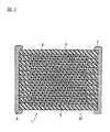
図1は本発明の一実施形態に係る積層セラミックコンデンサの断面図である。
Hereinafter, the present invention will be described based on embodiments shown in the drawings.
FIG. 1 is a cross-sectional view of a multilayer ceramic capacitor according to an embodiment of the present invention.
積層セラミックコンデンサ1
図1に示すように、本発明の一実施形態に係る積層セラミックコンデンサ1は、誘電体層2と内部電極層3とが交互に積層された構成のコンデンサ素子本体10を有する。このコンデンサ素子本体10の両端部には、素子本体10の内部で交互に配置された内部電極層3と各々導通する一対の外部電極4が形成してある。コンデンサ素子本体10の形状に特に制限はないが、通常、直方体状とされる。また、その寸法にも特に制限はなく、用途に応じて適当な寸法とすればよい。
Multilayer ceramic capacitor 1
As shown in FIG. 1, a multilayer ceramic capacitor 1 according to an embodiment of the present invention includes a
内部電極層3は、各端面がコンデンサ素子本体10の対向する2端部の表面に交互に露出するように積層してある。一対の外部電極4は、コンデンサ素子本体10の両端部に形成され、交互に配置された内部電極層3の露出端面に接続されて、コンデンサ回路を構成する。
The internal electrode layers 3 are laminated so that the end faces are alternately exposed on the surfaces of the two opposite ends of the
誘電体層2
誘電体層2は、本発明の誘電体磁器組成物を含有する。
誘電体層2に含有される誘電体磁器組成物は、BaTiO3 、SrTiO3 およびCaTiO3 を含む主成分を有する。
Dielectric layer 2
The dielectric layer 2 contains the dielectric ceramic composition of the present invention.
The dielectric ceramic composition contained in the dielectric layer 2 has a main component including BaTiO 3 , SrTiO 3 and CaTiO 3 .
本実施形態において、主成分を構成する上記BaTiO3 、SrTiO3 およびCaTiO3 は、それぞれ互いに、実質的に固溶していない状態で含有されている。すなわち、本実施形態では、これらBaTiO3 、SrTiO3 およびCaTiO3 は、それぞれ別々の結晶粒子としてのBaTiO3 結晶粒子、SrTiO3 結晶粒子およびCaTiO3 結晶粒子として含有され、コンポジット構造を形成している。 In the present embodiment, the BaTiO 3 , SrTiO 3 and CaTiO 3 constituting the main component are contained in a state where they are not substantially dissolved in each other. That is, in this embodiment, these BaTiO 3 , SrTiO 3 and CaTiO 3 are contained as BaTiO 3 crystal particles, SrTiO 3 crystal particles and CaTiO 3 crystal particles as separate crystal particles, respectively, and form a composite structure. .
ただし、BaTiO3 、SrTiO3 およびCaTiO3 は、実質的にBaTiO3 結晶粒子、SrTiO3 結晶粒子およびCaTiO3 結晶粒子として含有されていれば良く、たとえば、BaTiO3 の結晶粒子とSrTiO3 の結晶粒子との界面付近においては、一部固溶相が形成されていても構わない。 However, BaTiO 3 , SrTiO 3 and CaTiO 3 may be substantially contained as BaTiO 3 crystal particles, SrTiO 3 crystal particles and CaTiO 3 crystal particles. For example, BaTiO 3 crystal particles and SrTiO 3 crystal particles In the vicinity of the interface, a part of the solid solution phase may be formed.
BaTiO3 、SrTiO3 およびCaTiO3 を、それぞれ互いに、実質的に固溶していない状態とし、コンポジット構造を形成させることにより、誘電率を維持しながら、容量温度特性の向上を図ることができ、特に、EIA規格のX6S特性(−55〜105℃、ΔC/C=±22%以内)を満足させることができる。なお、この理由としては、たとえば、非固溶とし、コンポジット構造とすることにより、BaTiO3 に由来するキュリー温度のピークが残存すること等によると考えられる。 By making BaTiO 3 , SrTiO 3 and CaTiO 3 into a state in which they are not substantially dissolved in each other and forming a composite structure, it is possible to improve the capacity-temperature characteristics while maintaining the dielectric constant, In particular, the X6S characteristic of the EIA standard (−55 to 105 ° C., ΔC / C = within ± 22%) can be satisfied. The reason for this is considered to be, for example, that the Curie temperature peak derived from BaTiO 3 remains due to the non-solid solution and the composite structure.
主成分を構成するBaTiO3 、SrTiO3 およびCaTiO3 が互いに固溶しているか否かについては、たとえば、誘電体層2のX線回折により確認することができる。具体的には、誘電体層2に対して、X線源にCu−Kα線を用いたX線回折を行い、2θ=30〜35°の範囲に、それぞれBaTiO3 、SrTiO3 およびCaTiO3 に起因する分離可能な3つの回折ピークが観測されるか否かにより確認することができる。なお、2θ=30〜35°の範囲に観測される回折ピークは、それぞれBaTiO3 の(110)面の回折ピーク、SrTiO3 の(110)面の回折ピーク、およびCaTiO3 の(121)面の回折ピークである。 Whether or not BaTiO 3 , SrTiO 3 and CaTiO 3 constituting the main component are dissolved in each other can be confirmed by, for example, X-ray diffraction of the dielectric layer 2. Specifically, the dielectric layer 2 is subjected to X-ray diffraction using Cu-Kα ray as an X-ray source, and BaTiO 3 , SrTiO 3 and CaTiO 3 are respectively obtained in the range of 2θ = 30 to 35 °. This can be confirmed by whether or not the resulting separable three diffraction peaks are observed. The diffraction peaks observed in the range of 2θ = 30 to 35 ° are the diffraction peak of the (110) plane of BaTiO 3 , the diffraction peak of the (110) plane of SrTiO 3 , and the (121) plane of CaTiO 3 , respectively. It is a diffraction peak.
さらに、本実施形態では、誘電体層2を構成するBaTiO3 結晶粒子、SrTiO3 結晶粒子およびCaTiO3 結晶粒子のうち、BaTiO3 結晶粒子の粒子径を所定の範囲としている。すなわち、BaTiO3 結晶粒子の平均結晶粒子径を0.2〜0.8μmの範囲、好ましくは0.2〜0.6μmの範囲としている。 Further, in the present embodiment, among the BaTiO 3 crystal particles, SrTiO 3 crystal particles, and CaTiO 3 crystal particles constituting the dielectric layer 2, the particle diameter of the BaTiO 3 crystal particles is set within a predetermined range. That is, the average crystal particle diameter of the BaTiO 3 crystal particles is in the range of 0.2 to 0.8 μm, preferably in the range of 0.2 to 0.6 μm.
BaTiO3 結晶粒子の平均結晶粒子径をこのような範囲とすることにより、DCバイアス特性を良好に保ちつつ、比誘電率のさらなる向上を実現することができる。そして、比誘電率の向上が可能となることにより、誘電体層2の積層数を余り増加させることなく、所望の容量を得ることができ、そのため、製造コストの増大を抑えつつ、コンデンサの小型化が可能となる。 By setting the average crystal particle diameter of the BaTiO 3 crystal particles in such a range, it is possible to further improve the relative dielectric constant while maintaining good DC bias characteristics. Since the dielectric constant can be improved, a desired capacitance can be obtained without increasing the number of laminated dielectric layers 2 so that the size of the capacitor can be reduced while suppressing an increase in manufacturing cost. Can be realized.
BaTiO3 結晶粒子の平均結晶粒子径が小さすぎると、比誘電率が低下してしまう。一方、大きすぎると、DCバイアス特性が悪化してしまう。なお、BaTiO3 結晶粒子の平均結晶粒子径を上記範囲とする方法としては、たとえば、焼結後にBaTiO3 結晶粒子となるBaTiO3 粉末として、後述する所定の平均粒子径を有するBaTiO3 粉末を用いる方法などが挙げられる。 If the average crystal particle size of the BaTiO 3 crystal particles is too small, the relative dielectric constant is lowered. On the other hand, if it is too large, the DC bias characteristics will deteriorate. Incidentally, the average crystal grain size of BaTiO 3 crystal grains as a method of the above-mentioned range, for example, as BaTiO 3 powder of a BaTiO 3 crystal particles after sintering, using BaTiO 3 powder having a predetermined average particle size to be described later The method etc. are mentioned.
BaTiO3 結晶粒子の平均結晶粒子径は、たとえば、誘電体層2についてSEM観察を行うことにより測定することができる。具体的には、まず、誘電体層2についてSEM観察を行い、誘電体層2のSEM像(反射電子像)を得る。そして、SEM像(反射電子像)より、誘電体層2を構成する複数の結晶粒子(すなわち、BaTiO3 、SrTiO3 およびCaTiO3 の各結晶粒子)のうち、実質的にBaTiO3 から構成されている結晶粒子を特定し、これをBaTiO3 結晶粒子とする。次いで、特定したBaTiO3 結晶粒子の形状を球と仮定して平均粒子径を測定し、これをBaTiO3 結晶粒子の平均結晶粒子径とすることができる。 The average crystal particle diameter of the BaTiO 3 crystal particles can be measured, for example, by performing SEM observation on the dielectric layer 2. Specifically, first, SEM observation is performed on the dielectric layer 2 to obtain an SEM image (reflection electron image) of the dielectric layer 2. From the SEM image (reflected electron image), a plurality of crystal particles (that is, each crystal particle of BaTiO 3 , SrTiO 3 and CaTiO 3 ) constituting the dielectric layer 2 are substantially composed of BaTiO 3. The crystal grains that are present are identified and used as BaTiO 3 crystal grains. Next, assuming that the shape of the specified BaTiO 3 crystal particles is a sphere, the average particle size is measured, and this can be used as the average crystal particle size of the BaTiO 3 crystal particles.
なお、BaTiO3 結晶粒子以外の結晶粒子である、SrTiO3 結晶粒子およびCaTiO3 結晶粒子の平均結晶粒子径は特に限定されないが、たとえば次のような範囲とすることが好ましい。すなわち、SrTiO3 結晶粒子の平均結晶粒子径は、好ましくは0.3〜2μm、より好ましくは0.5〜1.5μmである。また、CaTiO3 結晶粒子の平均結晶粒子径は、好ましくは0.3〜2μm、より好ましくは0.8〜1.5μmである。これらSrTiO3 結晶粒子およびCaTiO3 結晶粒子の平均結晶粒子径は、上記したBaTiO3 結晶粒子と同様の方法により測定することができる。 In addition, although the average crystal particle diameter of SrTiO 3 crystal particles and CaTiO 3 crystal particles, which are crystal particles other than BaTiO 3 crystal particles, is not particularly limited, for example, the following ranges are preferable. That is, the average crystal particle diameter of the SrTiO 3 crystal particles is preferably 0.3 to 2 μm, more preferably 0.5 to 1.5 μm. Further, the average crystal particle diameter of the CaTiO 3 crystal particles is preferably 0.3 to 2 μm, more preferably 0.8 to 1.5 μm. The average crystal particle diameter of these SrTiO 3 crystal particles and CaTiO 3 crystal particles can be measured by the same method as that for the BaTiO 3 crystal particles described above.
また、主成分を構成するBaTiO3 、SrTiO3 およびCaTiO3 の組成モル比については特に限定されないが、これらを組成式{(Bax Sry Caz)O}m TiO2 で示した場合に、前記式中の記号x、y、zおよびmが、好ましくは、
0.19≦x≦0.23、
0.25≦y≦0.31、
0.46≦z≦0.54、
0.980≦m≦1.01、
であり、より好ましくは、
0.195≦x≦0.225、
0.255≦y≦0.305、
0.465≦z≦0.535、
0.985≦m≦1.0095、
である。なお、上記式において、x+y+z=1である。
記号x、y、zおよびmを上記範囲とすることにより、DCバイアス特性の向上効果と、電圧印加時における電歪量の低減効果と、を高めることができる。また、上記組成式において、酸素(O)量は、上記式の化学量論組成から若干偏倚してもよい。
Further, when there is no particular limitation on the composition molar ratio of BaTiO 3, SrTiO 3 and CaTiO 3 that constitute the main component, showing them by a composition formula {(Ba x Sr y Ca z ) O} m TiO 2, The symbols x, y, z and m in the above formula are preferably
0.19 ≦ x ≦ 0.23,
0.25 ≦ y ≦ 0.31,
0.46 ≦ z ≦ 0.54,
0.980 ≦ m ≦ 1.01,
And more preferably
0.195 ≦ x ≦ 0.225,
0.255 ≦ y ≦ 0.305,
0.465 ≦ z ≦ 0.535,
0.985 ≦ m ≦ 1.075,
It is. In the above formula, x + y + z = 1.
By making the symbols x, y, z, and m within the above ranges, it is possible to enhance the effect of improving the DC bias characteristics and the effect of reducing the amount of electrostriction during voltage application. In the above composition formula, the amount of oxygen (O) may be slightly deviated from the stoichiometric composition of the above formula.
上記式中、xは、BaTiO3 の含有割合を示す。主成分中のBaTiO3 の含有量が増加すると、強誘電性が強くなる傾向にある。xが小さ過ぎると、比誘電率が低くなってしまう傾向にある。特に、比誘電率が低すぎる場合には、所望の容量を得るためには、誘電体層2の積層数を増加させる必要が生じてくるため、製造コストが増加してしまうという問題や、コンデンサの小型化が困難となってしまうという問題が発生してしまう。一方、xが大き過ぎると、比誘電率は向上するものの、電圧印加時の電歪量が高くなり、さらにはDCバイアス特性が悪化する傾向にある。 In the above formula, x represents the content ratio of BaTiO 3 . As the content of BaTiO 3 in the main component increases, the ferroelectricity tends to increase. If x is too small, the relative permittivity tends to be low. In particular, if the relative dielectric constant is too low, it is necessary to increase the number of laminated dielectric layers 2 in order to obtain a desired capacitance. Therefore, there arises a problem that it becomes difficult to reduce the size. On the other hand, if x is too large, although the relative permittivity is improved, the amount of electrostriction when a voltage is applied increases, and the DC bias characteristics tend to deteriorate.
上記式中、yは、SrTiO3 の含有割合を示す。主成分中のSrTiO3 の含有量が増加すると、常誘電性が強くなる傾向にある。yが小さ過ぎると、比誘電率が低くなってしまう傾向にある。一方、yが大き過ぎると、DCバイアス特性が悪化する傾向にある。 In the above formula, y represents the content ratio of SrTiO 3 . When the content of SrTiO 3 in the main component increases, the paraelectric property tends to increase. If y is too small, the dielectric constant tends to be low. On the other hand, if y is too large, the DC bias characteristics tend to deteriorate.
上記式中、zは、CaTiO3 の含有割合を示す。CaTiO3 は、主に焼結安定性を向上させる効果や、絶縁抵抗値を向上させる効果を有する。zが小さ過ぎると、DCバイアス特性が悪化する傾向にある。一方、zが大き過ぎると、比誘電率が低下してしまう傾向にある。 In the above formula, z indicates the content of CaTiO 3. CaTiO 3 mainly has the effect of improving the sintering stability and the effect of improving the insulation resistance value. If z is too small, the DC bias characteristics tend to deteriorate. On the other hand, if z is too large, the dielectric constant tends to decrease.
主成分中のBaTiO3 の含有量が増加すると、強誘電性が強くなる一方で、主成分中のSrTiO3 ,CaTiO3 の含有量が増加すると、常誘電性が強くなる傾向にあり、記号x、y、zを上記範囲とすることにより、強誘電相と常誘電相とのバランスを図ることができる。 When the content of BaTiO 3 in the main component increases, the ferroelectricity becomes stronger. On the other hand, when the content of SrTiO 3 and CaTiO 3 in the main component increases, the paraelectric property tends to increase, and the symbol x By setting, y, and z within the above ranges, a balance between the ferroelectric phase and the paraelectric phase can be achieved.
上記式中、mは、ペロブスカイト構造のAサイトと、Bサイトと、の比(Ba,SrおよびCaと、Tiと、の比)を示す。mを0.980以上とすることにより、焼成時における誘電体粒子の粒成長を抑制することができる。また、mを1.01以下とすることにより、焼成温度を高くしなくても緻密な焼結体を得ることができる。mが小さすぎると、誘電体粒子の微細化が困難となり、DCバイアス特性が悪化する傾向にある。一方、mが大きすぎると、焼結温度が高くなり過ぎてしまい、焼結が困難となる傾向にある。 In the above formula, m represents the ratio of the A site of the perovskite structure to the B site (ratio of Ba, Sr and Ca and Ti). By setting m to 0.980 or more, the grain growth of dielectric particles during firing can be suppressed. Further, by setting m to 1.01 or less, a dense sintered body can be obtained without increasing the firing temperature. If m is too small, it is difficult to make the dielectric particles fine, and the DC bias characteristics tend to deteriorate. On the other hand, if m is too large, the sintering temperature becomes too high and sintering tends to be difficult.
上記誘電体磁器組成物には、上記した主成分に加えて、副成分がさらに含有されていることが好ましい。
本実施形態においては、副成分として、Mnの酸化物と、Siの酸化物と、V、Ta、Nb、W、MoおよびCrの各元素の酸化物から選択される1種以上と、をさらに含有していることが好ましい。
The dielectric ceramic composition preferably further contains subcomponents in addition to the main components described above.
In the present embodiment, as subcomponents, an oxide of Mn, an oxide of Si, and at least one selected from oxides of elements of V, Ta, Nb, W, Mo, and Cr are further included. It is preferable to contain.
Mnの酸化物は、焼結を促進する効果、および高温負荷寿命を改善する効果を有する。Mnの酸化物の含有量は、上記主成分100モルに対して、MnO換算で、好ましくは0.3〜1モルであり、より好ましくは0.3〜0.8モルである。Mnの酸化物の含有量が少な過ぎると、焼結性が悪化するとともに、高温負荷寿命に劣る傾向にある。一方、含有量が多過ぎると、IR不良率が悪化してしまう場合がある。 The oxide of Mn has the effect of promoting sintering and the effect of improving the high temperature load life. The content of the Mn oxide is preferably 0.3 to 1 mol and more preferably 0.3 to 0.8 mol in terms of MnO with respect to 100 mol of the main component. If the content of the Mn oxide is too small, the sinterability deteriorates and the high temperature load life tends to be inferior. On the other hand, if the content is too large, the IR defect rate may deteriorate.
Siの酸化物は、主として焼結助剤として作用するが、薄層化した際の初期絶縁抵抗の不良率を改善する効果を有する。Siの酸化物の含有量は、上記主成分100モルに対して、SiO2 換算で、好ましくは0.1〜0.5モルであり、より好ましくは0.15〜0.45モルである。Siの酸化物の含有量が少な過ぎると、焼成温度が上昇してしまう場合がある。一方、多過ぎると、IR不良率が悪化してしまう傾向にある。 The Si oxide mainly acts as a sintering aid, but has an effect of improving the defective rate of the initial insulation resistance when the layer is thinned. The content of the Si oxide is preferably 0.1 to 0.5 mol and more preferably 0.15 to 0.45 mol in terms of SiO 2 with respect to 100 mol of the main component. If the content of Si oxide is too small, the firing temperature may increase. On the other hand, when the amount is too large, the IR defect rate tends to deteriorate.
なお、本実施形態においては、Siの酸化物を複合酸化物の形態で含有させても良い。このような複合酸化物としては、SiO2 と、誘電体磁器組成物に含有される他の主成分や副成分を構成する元素の酸化物と、の複合酸化物が挙げられ、たとえば、CaSiO3 、SrSiO3 、(Ca,Sr)SiO3 、MnSiO3 、BaSiO3 などが挙げられる。これら複合酸化物を使用する場合には、焼成後の組成が所望の範囲となるように、適宜調整すればよい。 In the present embodiment, Si oxide may be included in the form of a complex oxide. Examples of such composite oxides include composite oxides of SiO 2 and oxides of elements constituting other main components and subcomponents contained in the dielectric ceramic composition. For example, CaSiO 3 , SrSiO 3 , (Ca, Sr) SiO 3 , MnSiO 3 , BaSiO 3 and the like. When these composite oxides are used, they may be appropriately adjusted so that the composition after firing falls within a desired range.
V、Ta、Nb、W、MoおよびCrの各元素の酸化物は、高温負荷寿命を改善する効果を有する。これらの酸化物の含有量は、主成分100モルに対して、V、Ta、Nb、W、MoおよびCrの各酸化物換算で、好ましくは、0.02モル以上、0.40モル未満、より好ましくは0.03〜0.30モル、さらに好ましくは0.05〜0.20モルである。これらの酸化物の含有量が少な過ぎると、上記効果が得難くなる。一方、多過ぎると、IRが低下する傾向にある。
なお、上記含有量は各元素換算の含有量であり、たとえば、Vの酸化物において、V元素換算での含有量が0.10モルである場合には、その酸化物であるV2 O5 換算での含有量は0.05モルとなる。
The oxides of each element of V, Ta, Nb, W, Mo, and Cr have an effect of improving the high temperature load life. The content of these oxides is preferably 0.02 mol or more and less than 0.40 mol in terms of each oxide of V, Ta, Nb, W, Mo and Cr with respect to 100 mol of the main component. More preferably, it is 0.03-0.30 mol, More preferably, it is 0.05-0.20 mol. If the content of these oxides is too small, the above effect is difficult to obtain. On the other hand, if too much, IR tends to decrease.
In addition, the said content is content of each element conversion, for example, in the oxide of V, when content in V element conversion is 0.10 mol, it is V 2 O 5 which is the oxide The content in terms of conversion is 0.05 mol.
また、本実施形態においては、必要に応じて、上記以外の副成分を含有させても良い。このような副成分としては、特に限定されないが、たとえば、Ba、Ca、Sr、Li、Mg、Al、Zr、Sc、Y、La、Ce、Pr、Nd、Pm、Sm、Eu、Gd、Tb、Dy、Ho、Er、Tm、YbおよびLuの各元素の酸化物などが挙げられる。 Moreover, in this embodiment, you may contain subcomponents other than the above as needed. Such subcomponents are not particularly limited. For example, Ba, Ca, Sr, Li, Mg, Al, Zr, Sc, Y, La, Ce, Pr, Nd, Pm, Sm, Eu, Gd, Tb , Dy, Ho, Er, Tm, Yb, and Lu oxides.
誘電体層2の厚みは、特に限定されないが、好ましくは1〜7μmであり、より好ましくは3〜6μmである。誘電体層2を薄くしすぎると、ショート不良率が悪化する場合がある。一方、厚くしすぎると、コンデンサの小型化が困難となってしまう。 Although the thickness of the dielectric material layer 2 is not specifically limited, Preferably it is 1-7 micrometers, More preferably, it is 3-6 micrometers. If the dielectric layer 2 is too thin, the short-circuit defect rate may deteriorate. On the other hand, if it is too thick, it is difficult to reduce the size of the capacitor.
内部電極層3
内部電極層3に含有される導電材は特に限定されないが、誘電体層2の構成材料が耐還元性を有するため、卑金属を用いることができる。導電材として用いる卑金属としては、Ni、Cu、Ni合金またはCu合金が好ましく、特にNiまたはNi合金が好ましい。内部電極層3の主成分をNiやNi合金とした場合には、誘電体が還元されないように、低酸素分圧(還元雰囲気)で焼成することが好ましい。内部電極層3の厚さは、好ましくは0.5〜2.0μm、より好ましくは0.7〜1.0μmである。
Internal electrode layer 3
The conductive material contained in the internal electrode layer 3 is not particularly limited, but a base metal can be used because the constituent material of the dielectric layer 2 has reduction resistance. As the base metal used as the conductive material, Ni, Cu, Ni alloy or Cu alloy is preferable, and Ni or Ni alloy is particularly preferable. When the main component of the internal electrode layer 3 is Ni or a Ni alloy, it is preferable to fire at a low oxygen partial pressure (reducing atmosphere) so that the dielectric is not reduced. The thickness of the internal electrode layer 3 is preferably 0.5 to 2.0 μm, more preferably 0.7 to 1.0 μm.
外部電極4
外部電極4に含有される導電材は特に限定されないが、本発明では安価なNi,Cuや、これらの合金を用いることができる。外部電極4の厚さは用途等に応じて適宜決定すればよい。
External electrode 4
The conductive material contained in the external electrode 4 is not particularly limited, but in the present invention, inexpensive Ni, Cu, and alloys thereof can be used. What is necessary is just to determine the thickness of the external electrode 4 suitably according to a use etc.
積層セラミックコンデンサ1の製造方法
本実施形態の積層セラミックコンデンサ1は、従来の積層セラミックコンデンサと同様に、ペーストを用いた通常の印刷法やシート法によりグリーンチップを作製し、これを焼成した後、外部電極を印刷または転写して焼成することにより製造される。以下、製造方法について具体的に説明する。
Manufacturing Method of Multilayer Ceramic Capacitor 1 The multilayer ceramic capacitor 1 of the present embodiment is the same as a conventional multilayer ceramic capacitor. After producing a green chip by a normal printing method or a sheet method using a paste and firing it, It is manufactured by printing or transferring an external electrode and firing. Hereinafter, the manufacturing method will be specifically described.
まず、誘電体層用ペーストに含まれる誘電体原料(誘電体磁器組成物粉末)を準備し、これを塗料化して、誘電体層用ペーストを調製する。 First, a dielectric material (dielectric ceramic composition powder) contained in the dielectric layer paste is prepared, and this is made into a paint to prepare a dielectric layer paste.
誘電体層用ペーストは、誘電体原料と有機ビヒクルとを混練した有機系の塗料であってもよく、水系の塗料であってもよい。 The dielectric layer paste may be an organic paint obtained by kneading a dielectric material and an organic vehicle, or may be a water-based paint.
誘電体原料としては、上記した主成分および副成分の酸化物やその混合物、複合酸化物を用いることができるが、その他、焼成により上記した酸化物や複合酸化物となる各種化合物、たとえば、炭酸塩、シュウ酸塩、硝酸塩、水酸化物、有機金属化合物等から適宜選択し、混合して用いることもできる。誘電体原料中の各化合物の含有量は、焼成後に上記した誘電体磁器組成物の組成となるように決定すればよい。塗料化する前の状態で、誘電体原料の粒径は、通常、平均粒径0.1〜1μm程度である。 As the dielectric material, the above-mentioned main component and subcomponent oxides, mixtures thereof, and composite oxides can be used. In addition, various compounds that become the above oxides or composite oxides by firing, such as carbonic acid, can be used. A salt, an oxalate salt, a nitrate salt, a hydroxide, an organometallic compound, or the like can be selected as appropriate and used in combination. What is necessary is just to determine content of each compound in a dielectric raw material so that it may become a composition of the above-mentioned dielectric ceramic composition after baking. In the state before forming a paint, the particle size of the dielectric material is usually about 0.1 to 1 μm in average particle size.
本実施形態では、上記主成分の原料として、BaTiO3 粉末、SrTiO3 粉末およびCaTiO3 粉末を使用することが好ましく、特に、これらのBaTiO3 粉末、SrTiO3 粉末、CaTiO3 粉末は、互いに予め反応させることなく用いることが好ましい。主成分の原料として、これらの粉末を使用し、しかも、予め互いに反応させることなく用いることにより、焼結後の誘電体磁器組成物において、主成分を構成することとなるBaTiO3 、SrTiO3 およびCaTiO3 を、それぞれ互いに、実質的に固溶していない構成とすることができる。すなわち、焼結後の誘電体磁器組成物において、これらの複合酸化物を、BaTiO3 結晶粒子、SrTiO3 結晶粒子およびCaTiO3 結晶粒子の形態で存在させ、コンポジット構造を形成させることができる。 In the present embodiment, it is preferable to use BaTiO 3 powder, SrTiO 3 powder and CaTiO 3 powder as the raw material of the main component. In particular, these BaTiO 3 powder, SrTiO 3 powder and CaTiO 3 powder react with each other in advance. It is preferable to use without making it. BaTiO 3 , SrTiO 3, and SrTiO 3 that constitute the main component in the sintered dielectric ceramic composition by using these powders as raw materials of the main component and using them without reacting with each other in advance. the CaTiO 3, each other, can be configured to not substantially dissolved. That is, in the sintered dielectric ceramic composition, these composite oxides can be present in the form of BaTiO 3 crystal particles, SrTiO 3 crystal particles, and CaTiO 3 crystal particles to form a composite structure.
しかも、本実施形態では、上記主成分の原料のうち、BaTiO3 粉末として、所定の平均粒子径を有するBaTiO3 粉末を使用する。具体的には、平均粒子径が0.1〜0.6μmの範囲、好ましくは0.2〜0.5μmの範囲にあるBaTiO3 粉末を使用する。このような範囲の平均粒子径を有するBaTiO3 粉末を用いることにより、焼成後の誘電体層2中における、BaTiO3 結晶粒子の平均結晶粒子径を上述した所定の範囲とすることができ、結果として、DCバイアス特性を良好に保ちつつ、比誘電率のさらなる向上を実現することができる。なお、BaTiO3 粉末の平均粒子径の測定方法としては、たとえば、レーザー回折法などの光散乱を利用した方法により体積基準累積50%径(D50径)を測定し、これを平均粒子径とする方法などが挙げられる。
また、上記BaTiO3 粉末としては、平均粒子径が上記範囲となっているとともに、ペロブスカイト構造のAサイト(Baサイト)と、B(Tiサイト)サイトと、の比であるA/Bが、好ましくは0.90〜1.10、特に0.95〜1.05である粉末を用いることが好ましい。
Moreover, in the present embodiment, among the main component raw materials, BaTiO 3 powder having a predetermined average particle diameter is used as the BaTiO 3 powder. Specifically, BaTiO 3 powder having an average particle diameter in the range of 0.1 to 0.6 μm, preferably in the range of 0.2 to 0.5 μm is used. By using the BaTiO 3 powder having an average particle size in such a range, the average crystal particle size of the BaTiO 3 crystal particles in the dielectric layer 2 after firing can be within the predetermined range described above, and the result As a result, the relative permittivity can be further improved while keeping the DC bias characteristics good. In addition, as a measuring method of the average particle diameter of BaTiO 3 powder, for example, a volume-based cumulative 50% diameter (D50 diameter) is measured by a method using light scattering such as a laser diffraction method, and this is used as the average particle diameter. The method etc. are mentioned.
Further, the BaTiO 3 powder preferably has an average particle diameter in the above range, and A / B which is a ratio of the A site (Ba site) and the B (Ti site) site of the perovskite structure is preferable. Is preferably 0.90 to 1.10, more preferably 0.95 to 1.05.
BaTiO3 粉末以外の主成分原料である、SrTiO3 粉末およびCaTiO3 粉末としては、特に限定されないが、たとえば、次のような範囲の平均粒子径を有する粉末を用いることが好ましい。すなわち、SrTiO3 粉末の平均粒子径が、好ましくは0.1〜0.6μm、より好ましくは0.2〜0.5μmである。また、CaTiO3 粉末の平均粒子径が、好ましくは0.1〜0.6μm、より好ましくは0.2〜0.5μmである。SrTiO3 粉末およびCaTiO3 粉末の平均粒子径は、上記したBaTiO3 粉末と同様の方法により測定することができる。 The SrTiO 3 powder and CaTiO 3 powder, which are the main component raw materials other than the BaTiO 3 powder, are not particularly limited. For example, it is preferable to use a powder having an average particle diameter in the following range. That is, the average particle diameter of the SrTiO 3 powder is preferably 0.1 to 0.6 μm, more preferably 0.2 to 0.5 μm. The average particle diameter of CaTiO 3 powder is preferably 0.1 to 0.6 .mu.m, more preferably 0.2 to 0.5 [mu] m. The average particle diameter of the SrTiO 3 powder and the CaTiO 3 powder can be measured by the same method as that for the BaTiO 3 powder described above.
なお、主成分原料としてのBaTiO3 粉末、SrTiO3 粉末、CaTiO3 粉末は、いわゆる固相法の他、各種液相法(たとえば、しゅう酸塩法、水熱合成法、アルコキシド法、ゾルゲル法など)により製造することができる。 In addition, BaTiO 3 powder, SrTiO 3 powder, and CaTiO 3 powder as the main component raw material are not only so-called solid phase methods but also various liquid phase methods (eg, oxalate method, hydrothermal synthesis method, alkoxide method, sol-gel method, etc. ).
本実施形態では、主成分原料粉末として、ペロブスカイト構造のAサイト成分がそれぞれ異なる3種類の原料粉末(すなわち、Ba、Sr、Caの3種類)を用いるため、このようにAサイト成分が異なることにより、互いにAサイト成分が異なる他の原料粉末(たとえば、BaTiO3 粉末とSrTiO3 粉末)同士の反応性が低いという特性を有している。しかも、Aサイト成分がそれぞれ異なる原料粉末を3種類用いているため、同じAサイト成分を有する粉末同士の接触点を少ないものとすることができる。 In this embodiment, since three kinds of raw material powders having different perovskite structure A site components (that is, three kinds of Ba, Sr, and Ca) are used as the main component raw material powder, the A site components are different in this way. Therefore, the other raw material powders (for example, BaTiO 3 powder and SrTiO 3 powder) having different A site components from each other have low reactivity. Moreover, since three types of raw material powders having different A site components are used, the number of contact points between the powders having the same A site component can be reduced.
なかでも、BaTiO3 粉末は、SrTiO3 粉末やCaTiO3 粉末との反応性が非常に低いという特性を有しているため、焼成時における粒成長を抑制することができ、そのため、原料粉末としてのBaTiO3 粉末の平均粒子径を調整することで、焼結後の誘電体層2中におけるBaTiO3 結晶粒子の平均結晶粒子径を所定の範囲とすることができる。特に、本実施形態では、たとえば、0.1μm以上、0.2μm未満程度と比較的小さな平均粒子径を有するBaTiO3 粉末を用いることも可能となる。 Among these, BaTiO 3 powder has a characteristic that the reactivity with SrTiO 3 powder and CaTiO 3 powder is very low, and thus it is possible to suppress grain growth at the time of firing. By adjusting the average particle size of the BaTiO 3 powder, the average crystal particle size of the BaTiO 3 crystal particles in the sintered dielectric layer 2 can be set within a predetermined range. In particular, in this embodiment, for example, it is possible to use BaTiO 3 powder having a relatively small average particle diameter of about 0.1 μm or more and less than 0.2 μm.
また、上記主成分以外の原料(たとえば、副成分の原料)としては、各酸化物や焼成により各酸化物となる化合物を、そのまま用いても良いし、あるいは、予め仮焼きし、焙焼粉として用いても良い。 In addition, as raw materials other than the main components (for example, raw materials for subcomponents), each oxide or a compound that becomes each oxide by firing may be used as it is, or calcined and roasted in advance. It may be used as
有機ビヒクルとは、バインダを有機溶剤中に溶解したものである。有機ビヒクルに用いるバインダは特に限定されず、エチルセルロース、ポリビニルブチラール等の通常の各種バインダから適宜選択すればよい。また、有機溶剤も特に限定されず、印刷法やシート法など、利用する方法に応じて、テルピネオール、ブチルカルビトール、アセトン、トルエン等の各種有機溶剤から適宜選択すればよい。 An organic vehicle is obtained by dissolving a binder in an organic solvent. The binder used for the organic vehicle is not particularly limited, and may be appropriately selected from usual various binders such as ethyl cellulose and polyvinyl butyral. Further, the organic solvent is not particularly limited, and may be appropriately selected from various organic solvents such as terpineol, butyl carbitol, acetone, toluene, and the like according to a method to be used such as a printing method or a sheet method.
また、誘電体層用ペーストを水系の塗料とする場合には、水溶性のバインダや分散剤などを水に溶解させた水系ビヒクルと、誘電体原料とを混練すればよい。水系ビヒクルに用いる水溶性バインダは特に限定されず、たとえば、ポリビニルアルコール、セルロース、水溶性アクリル樹脂などを用いればよい。 Further, when the dielectric layer paste is used as a water-based paint, a water-based vehicle in which a water-soluble binder or a dispersant is dissolved in water and a dielectric material may be kneaded. The water-soluble binder used for the water-based vehicle is not particularly limited, and for example, polyvinyl alcohol, cellulose, water-soluble acrylic resin, etc. may be used.
内部電極層用ペーストは、上記した各種導電性金属や合金からなる導電材、あるいは焼成後に上記した導電材となる各種酸化物、有機金属化合物、レジネート等と、上記した有機ビヒクルとを混練して調製する。なお、内部電極層用ペーストとしては、市販の電極用ペーストを使用してもよいし、あるいは市販の電極用材料をペースト化したものを使用してもよい。また、内部電極層用ペーストには、必要に応じて共材を含有させても良い。共材としては、誘電体層用ペーストに含まれる誘電体原料と同様の組成を有するもの(たとえば、BaTiO3 粉末、SrTiO3 粉末、CaTiO3 粉末等)を使用すれば良い。 The internal electrode layer paste is obtained by kneading the above-mentioned organic vehicle with various conductive metals and alloys as described above, or various oxides, organometallic compounds, resinates, etc. that become the above-mentioned conductive materials after firing. Prepare. As the internal electrode layer paste, a commercially available electrode paste may be used, or a paste prepared from a commercially available electrode material may be used. In addition, the internal electrode layer paste may contain a co-material as necessary. As the co-material, a material having the same composition as the dielectric material contained in the dielectric layer paste (for example, BaTiO 3 powder, SrTiO 3 powder, CaTiO 3 powder, etc.) may be used.
外部電極用ペーストは、上記した内部電極層用ペーストと同様にして調製すればよい。 The external electrode paste may be prepared in the same manner as the internal electrode layer paste described above.
上記した各ペースト中の有機ビヒクルの含有量に特に制限はなく、通常の含有量、たとえば、バインダは1〜5重量%程度、溶剤は10〜50重量%程度とすればよい。また、各ペースト中には、必要に応じて各種分散剤、可塑剤、誘電体、絶縁体等から選択される添加物が含有されていてもよい。これらの総含有量は、10重量%以下とすることが好ましい。 There is no restriction | limiting in particular in content of the organic vehicle in each above-mentioned paste, For example, what is necessary is just about 1-5 weight% of binders, for example, about 10-50 weight% of binders. Each paste may contain additives selected from various dispersants, plasticizers, dielectrics, insulators, and the like as necessary. The total content of these is preferably 10% by weight or less.
印刷法を用いる場合、誘電体層用ペーストおよび内部電極層用ペーストを、PET等の基板上に印刷、積層し、所定形状に切断した後、基板から剥離してグリーンチップとする。 When the printing method is used, the dielectric layer paste and the internal electrode layer paste are printed and laminated on a substrate such as PET, cut into a predetermined shape, and then peeled from the substrate to obtain a green chip.
また、シート法を用いる場合、誘電体層用ペーストを用いてグリーンシートを形成し、この上に内部電極層用ペーストを印刷した後、これらを積層してグリーンチップとする。 When the sheet method is used, a dielectric layer paste is used to form a green sheet, the internal electrode layer paste is printed thereon, and these are stacked to form a green chip.
焼成前に、グリーンチップに脱バインダ処理を施す。脱バインダ条件としては、昇温速度を好ましくは5〜300℃/時間、保持温度を好ましくは180〜400℃、温度保持時間を好ましくは0.5〜24時間とする。また、焼成雰囲気は、空気もしくは還元性雰囲気とする。 Before firing, the green chip is subjected to binder removal processing. As binder removal conditions, the temperature rising rate is preferably 5 to 300 ° C./hour, the holding temperature is preferably 180 to 400 ° C., and the temperature holding time is preferably 0.5 to 24 hours. The firing atmosphere is air or a reducing atmosphere.
グリーンチップ焼成時の雰囲気は、内部電極層用ペースト中の導電材の種類に応じて適宜決定されればよいが、導電材としてNiやNi合金等の卑金属を用いる場合、焼成雰囲気中の酸素分圧は、1.2×10⁻⁷〜3.2×10⁻⁴Paとすることが好ましい。酸素分圧が上記範囲未満であると、内部電極層の導電材が異常焼結を起こし、途切れてしまうことがある。また、酸素分圧が前記範囲を超えると、内部電極層が酸化する傾向にある。 The atmosphere at the time of green chip firing may be appropriately determined according to the type of conductive material in the internal electrode layer paste, but when a base metal such as Ni or Ni alloy is used as the conductive material, the oxygen content in the firing atmosphere The pressure is preferably 1.2 × 10 −7 to 3.2 × 10 −4 Pa. When the oxygen partial pressure is less than the above range, the conductive material of the internal electrode layer may be abnormally sintered and may be interrupted. Further, when the oxygen partial pressure exceeds the above range, the internal electrode layer tends to be oxidized.
また、焼成時の保持温度は、好ましくは1000〜1400℃、より好ましくは1100〜1360℃である。保持温度が上記範囲未満であると緻密化が不十分となり、前記範囲を超えると、内部電極層の異常焼結による電極の途切れや、内部電極層構成材料の拡散による容量温度特性の悪化、誘電体磁器組成物の還元が生じやすくなる。 Moreover, the holding temperature at the time of baking becomes like this. Preferably it is 1000-1400 degreeC, More preferably, it is 1100-1360 degreeC. If the holding temperature is lower than the above range, the densification becomes insufficient. If the holding temperature is higher than the above range, the electrode is interrupted due to abnormal sintering of the internal electrode layer, the capacity temperature characteristic is deteriorated due to diffusion of the constituent material of the internal electrode layer, the dielectric Reduction of the body porcelain composition is likely to occur.
これ以外の焼成条件としては、昇温速度を好ましくは50〜500℃/時間、より好ましくは200〜300℃/時間、温度保持時間を好ましくは0.5〜8時間、より好ましくは1〜3時間、冷却速度を好ましくは50〜500℃/時間、より好ましくは200〜300℃/時間とする。また、焼成雰囲気は還元性雰囲気とすることが好ましく、雰囲気ガスとしてはたとえば、N2 とH2 との混合ガスを加湿して用いることができる。 As other firing conditions, the rate of temperature rise is preferably 50 to 500 ° C./hour, more preferably 200 to 300 ° C./hour, and the temperature holding time is preferably 0.5 to 8 hours, more preferably 1 to 3 hours. The time and cooling rate are preferably 50 to 500 ° C./hour, more preferably 200 to 300 ° C./hour. Further, the firing atmosphere is preferably a reducing atmosphere, and as the atmosphere gas, for example, a mixed gas of N 2 and H 2 can be used by humidification.
還元性雰囲気中で焼成した場合、コンデンサ素子本体にはアニールを施すことが好ましい。アニールは、誘電体層を再酸化するための処理であり、これによりIR寿命を著しく長くすることができるので、信頼性が向上する。 When firing in a reducing atmosphere, it is preferable to anneal the capacitor element body. Annealing is a process for re-oxidizing the dielectric layer, and this can significantly increase the IR lifetime, thereby improving the reliability.
アニール雰囲気中の酸素分圧は、10−1〜10Paとすることが好ましい。酸素分圧が前記範囲未満であると誘電体層の再酸化が困難であり、前記範囲を超えると内部電極層の酸化が進行する傾向にある。 The oxygen partial pressure in the annealing atmosphere is preferably 10 −1 to 10 Pa. When the oxygen partial pressure is less than the above range, it is difficult to re-oxidize the dielectric layer, and when it exceeds the above range, oxidation of the internal electrode layer tends to proceed.
アニールの際の保持温度は、1100℃以下、特に500〜1100℃とすることが好ましい。保持温度が上記範囲未満であると誘電体層の酸化が不十分となるので、IRが低く、また、高温負荷寿命が短くなりやすい。一方、保持温度が前記範囲を超えると、内部電極層が酸化して容量が低下するだけでなく、内部電極層が誘電体素地と反応してしまい、容量温度特性の悪化、IRの低下、高温負荷寿命の低下が生じやすくなる。なお、アニールは昇温過程および降温過程だけから構成してもよい。すなわち、温度保持時間を零としてもよい。この場合、保持温度は最高温度と同義である。 The holding temperature at the time of annealing is preferably 1100 ° C. or less, particularly 500 to 1100 ° C. When the holding temperature is lower than the above range, the dielectric layer is not sufficiently oxidized, so that the IR is low and the high temperature load life is likely to be shortened. On the other hand, when the holding temperature exceeds the above range, not only the internal electrode layer is oxidized and the capacity is lowered, but the internal electrode layer reacts with the dielectric substrate, the capacity temperature characteristic is deteriorated, the IR is lowered, the high temperature The load life is likely to decrease. Note that annealing may be composed of only a temperature raising process and a temperature lowering process. That is, the temperature holding time may be zero. In this case, the holding temperature is synonymous with the maximum temperature.
これ以外のアニール条件としては、温度保持時間を好ましくは0〜20時間、より好ましくは2〜10時間、冷却速度を好ましくは50〜500℃/時間、より好ましくは100〜300℃/時間とする。また、アニールの雰囲気ガスとしては、たとえば、加湿したN2 ガス等を用いることが好ましい。 As other annealing conditions, the temperature holding time is preferably 0 to 20 hours, more preferably 2 to 10 hours, and the cooling rate is preferably 50 to 500 ° C./hour, more preferably 100 to 300 ° C./hour. . Further, as the annealing atmosphere gas, for example, humidified N 2 gas or the like is preferably used.
上記した脱バインダ処理、焼成およびアニールにおいて、N2 ガスや混合ガス等を加湿するには、たとえばウェッター等を使用すればよい。この場合、水温は5〜75℃程度が好ましい。
脱バインダ処理、焼成およびアニールは、連続して行なっても、独立に行なってもよい。
In the above-described binder removal processing, firing and annealing, for example, a wetter or the like may be used to wet the N 2 gas or mixed gas. In this case, the water temperature is preferably about 5 to 75 ° C.
The binder removal treatment, firing and annealing may be performed continuously or independently.
上記のようにして得られたコンデンサ素子本体に、例えばバレル研磨やサンドブラストなどにより端面研磨を施し、外部電極用ペーストを塗布して焼成し、外部電極4を形成する。そして、必要に応じ、外部電極4表面に、めっき等により被覆層を形成する。
このようにして製造された本実施形態の積層セラミックコンデンサは、ハンダ付等によりプリント基板上などに実装され、各種電子機器等に使用される。
The capacitor element main body obtained as described above is subjected to end face polishing, for example, by barrel polishing or sand blasting, and the external electrode paste is applied and fired to form the external electrode 4. Then, if necessary, a coating layer is formed on the surface of the external electrode 4 by plating or the like.
The multilayer ceramic capacitor of this embodiment manufactured in this way is mounted on a printed circuit board or the like by soldering or the like and used for various electronic devices.
本実施形態によれば、積層セラミックコンデンサの誘電体層2を、上記した誘電体磁器組成物で構成する。そのため、本実施形態の積層セラミックコンデンサは、容量温度特性に優れ、電圧印加時における電歪量の低減されており、しかも、DCバイアス特性(誘電率の直流電圧印加依存性)を良好に保ちながら、高い比誘電率を実現することができる。特に、容量温度特性については、EIA規格のX6S特性(−55〜105℃、ΔC/C=±22%以内)を満足させることができる。 According to the present embodiment, the dielectric layer 2 of the multilayer ceramic capacitor is composed of the above-described dielectric ceramic composition. Therefore, the multilayer ceramic capacitor of this embodiment has excellent capacitance-temperature characteristics, a reduced amount of electrostriction when a voltage is applied, and while maintaining good DC bias characteristics (dependence of dielectric constant on DC voltage application). High dielectric constant can be realized. In particular, with respect to the capacity-temperature characteristic, the X6S characteristic of the EIA standard (−55 to 105 ° C., ΔC / C = within ± 22%) can be satisfied.
なお、本実施形態では、上記電圧印加時における電歪量に関し、以下のような特性を有する。
すなわち、一対の内部電極層3に挟まれている誘電体層2の層数をN層とした場合に、セラミックコンデンサを基板に固定し、ガラスエポキシ基板などの積層セラミックコンデンサ1が実装されるような通常の基板に固定したセラミックコンデンサに対し、AC:0.2Vrms/μm、DC:4V/μm、周波数:1kHzの条件で電圧を印加した際における素子本体10表面の振動幅で定義される電歪量を、好ましくは、0.125N[nm]未満、より好ましくは0.1N[nm]以下とすることができる。
特に、本実施形態では、500以上という高い誘電率を実現しつつ、電圧印加時における電歪量を上記範囲とすることができる。
In the present embodiment, the electrostriction amount when the voltage is applied has the following characteristics.
That is, when the number of dielectric layers 2 sandwiched between the pair of internal electrode layers 3 is N, the ceramic capacitor is fixed to the substrate, and the multilayer ceramic capacitor 1 such as a glass epoxy substrate is mounted. A voltage defined by the vibration width of the surface of the
In particular, in the present embodiment, the amount of electrostriction when a voltage is applied can be within the above range while realizing a high dielectric constant of 500 or more.
上記電圧印加条件における、AC、DCの値は、誘電体層の厚み1μm当たりの印加電圧である。すなわち、たとえば、誘電体層の厚みを5μmとした場合における印加電圧は、AC:1.0Vrms(=0.2Vrms/μm×5μm)、DC:20V(=4V/μm×5μm)である。また、上記電歪量は、誘電体層2の厚みが変化すると、それに伴い変化する傾向にある。そのため、本実施形態においては、誘電体層2の厚みが、好ましくは1〜7μm、より好ましくは3〜6μm、特に5μmの場合に、上記所定範囲となることが好ましい。 The values of AC and DC under the above voltage application conditions are applied voltages per 1 μm thickness of the dielectric layer. That is, for example, when the thickness of the dielectric layer is 5 μm, the applied voltage is AC: 1.0 Vrms (= 0.2 Vrms / μm × 5 μm) and DC: 20 V (= 4 V / μm × 5 μm). Further, the amount of electrostriction tends to change as the thickness of the dielectric layer 2 changes. Therefore, in this embodiment, when the thickness of the dielectric layer 2 is preferably 1 to 7 [mu] m, more preferably 3 to 6 [mu] m, and particularly 5 [mu] m, the predetermined range is preferable.
以上、本発明の実施形態について説明してきたが、本発明は、上述した実施形態に何等限定されるものではなく、本発明の要旨を逸脱しない範囲内において種々に改変することができる。 As mentioned above, although embodiment of this invention has been described, this invention is not limited to the embodiment mentioned above at all, and can be variously modified within the range which does not deviate from the summary of this invention.
たとえば、上述した実施形態では、本発明に係る電子部品として積層セラミックコンデンサを例示したが、本発明に係る電子部品としては、積層セラミックコンデンサに限定されず、上記構成の誘電体層を有するものであれば何でも良い。 For example, in the above-described embodiment, the multilayer ceramic capacitor is exemplified as the electronic component according to the present invention. However, the electronic component according to the present invention is not limited to the multilayer ceramic capacitor, and has a dielectric layer having the above configuration. Anything is fine.
以下、本発明を、さらに詳細な実施例に基づき説明するが、本発明は、これら実施例に限定されない。 Hereinafter, although this invention is demonstrated based on a more detailed Example, this invention is not limited to these Examples.
実施例1
まず、主成分の原料として、BaTiO3 粉末、SrTiO3 粉末およびCaTiO3 粉末を、副成分の原料として、MnCO3 (焼成後にMnOとなる化合物)、V2 O5 、SiO2 を、それぞれ準備した。なお、主成分の原料としてのBaTiO3 粉末、SrTiO3 粉末およびCaTiO3 粉末としては、表1に示す各平均粒子径を有する粉末を用いた。
また、本実施例で用いたBaTiO3 粉末、SrTiO3 粉末およびCaTiO3 粉末の、ペロブスカイト構造のAサイトと、Bサイトと、の比であるA/Bは以下の通りである。
BaTiO3 粉末のA/B=1.003
SrTiO3 粉末のA/B=1.003
CaTiO3 粉末のA/B=1.003
Example 1
First, BaTiO 3 powder, SrTiO 3 powder and CaTiO 3 powder were prepared as main component materials, and MnCO 3 (compound which becomes MnO after firing), V 2 O 5 and SiO 2 were prepared as subcomponent materials, respectively. . Incidentally, as the BaTiO 3 powder, SrTiO 3 powder and CaTiO 3 powder as raw materials of the main component, powders having respective average particle diameters shown in Table 1 were used.
A / B, which is the ratio of the perovskite structure A site to the B site of the BaTiO 3 powder, SrTiO 3 powder, and CaTiO 3 powder used in this example, is as follows.
A / B of BaTiO 3 powder = 1.003
A / B of SrTiO 3 powder = 1.003
A / B of CaTiO 3 powder = 1.003
次いで、上記にて準備した各原料を、ボールミルで15時間、湿式粉砕し、乾燥して、誘電体材料を得た。なお、各原料の混合割合は、次の通りとした。
すなわち、主成分原料の混合比を、重量比で、BaTiO3 粉末:SrTiO3 粉末:CaTiO3 粉末=0.2:0.3:0.5とした。また、主成分100モルに対する各副成分の割合を、MnO:0.5モル、V2 O5 :0.1モル、SiO2 :0.22モルとした(ただし、MnO、SiO2 については各酸化物換算でのモル数であり、V2 O5 についてはV元素換算でのモル数である。)。
Subsequently, each raw material prepared above was wet pulverized with a ball mill for 15 hours and dried to obtain a dielectric material. In addition, the mixing ratio of each raw material was as follows.
That is, the mixing ratio of the main component raw materials was BaTiO 3 powder: SrTiO 3 powder: CaTiO 3 powder = 0.2: 0.3: 0.5 by weight. Moreover, the ratio of each subcomponent with respect to 100 mol of the main components was MnO: 0.5 mol, V 2 O 5 : 0.1 mol, and SiO 2 : 0.22 mol (however, each of MnO and SiO 2 It is the number of moles in terms of oxide, and V 2 O 5 is the number of moles in terms of V element.)
次いで、得られた誘電体材料100重量部と、ポリビニルブチラール樹脂10重量部と、可塑剤としてのジブチルフタレート(DOP)5重量部と、溶媒としてのアルコール100重量部とをボールミルで混合してペースト化し、誘電体層用ペーストを得た。 Next, 100 parts by weight of the obtained dielectric material, 10 parts by weight of polyvinyl butyral resin, 5 parts by weight of dibutyl phthalate (DOP) as a plasticizer, and 100 parts by weight of alcohol as a solvent were mixed with a ball mill to obtain a paste. To obtain a dielectric layer paste.
また、本実施例においては内部電極層用ペーストとして、コンデンサ電極用のペースト(導電性粒子として、主にNi粒子を含有するペースト)を使用した。 In this example, a capacitor electrode paste (a paste mainly containing Ni particles as conductive particles) was used as the internal electrode layer paste.
これらのペーストを用い、以下のようにして、図1に示される積層型セラミックチップコンデンサ1を製造した。 Using these pastes, the multilayer ceramic chip capacitor 1 shown in FIG. 1 was manufactured as follows.
まず、得られた誘電体層用ペーストを用いて、ドクターブレード法にて、PETフィルム上に、グリーンシートを形成した。次いで、このグリーンシートの上に、内部電極層用ペーストを用いて、スクリーン印刷により、電極パターンを印刷し、電極パターンの印刷されたグリーンシートを製造した。なお、電極パターンの印刷されたグリーンシートの厚みは、乾燥後の厚みで6μmとした。次いで、上記のグリーンシートとは別に、誘電体層用ペーストを用いて、ドクターブレード法にて、PETフィルム上に電極パターンの印刷されていないグリーンシートを製造した。 First, a green sheet was formed on a PET film by the doctor blade method using the obtained dielectric layer paste. Next, an electrode pattern was printed on the green sheet by screen printing using the internal electrode layer paste to produce a green sheet on which the electrode pattern was printed. The thickness of the green sheet on which the electrode pattern was printed was 6 μm after drying. Next, separately from the above green sheet, a green sheet with no electrode pattern printed on the PET film was manufactured by a doctor blade method using the dielectric layer paste.
そして、上記にて製造した各グリーンシートを次の順序にて積層し、得られた積層体を加圧することにより、グリーンチップを製造した。
すなわち、まず、電極パターンの印刷されていないグリーンシートを合計の厚みが300μmとなるまで積層した。その上に、電極パターンの印刷されたグリーンシートを5枚積層した。さらにその上に、電極パターンの印刷されていないグリーンシートを合計の厚さが300μmとなるまで積層し、積層体とした。そして、得られた積層体について、温度80℃、圧力1t/cm2の条件で加熱・加圧して、グリーンチップを得た。
And each green sheet manufactured above was laminated | stacked in the following order, and the green chip | tip was manufactured by pressing the obtained laminated body.
That is, first, green sheets on which no electrode patterns were printed were laminated until the total thickness reached 300 μm. On top of that, five green sheets printed with electrode patterns were laminated. Further thereon, a green sheet on which no electrode pattern was printed was laminated until the total thickness reached 300 μm to obtain a laminate. The obtained laminate was heated and pressurized under the conditions of a temperature of 80 ° C. and a pressure of 1 t / cm 2 to obtain a green chip.
次いで、得られたグリーンチップを所定のサイズに切断し、脱バインダ処理、焼成およびアニールを下記条件にて行って、積層セラミック焼成体を得た。
脱バインダ処理条件は、昇温速度:30℃/時間、保持温度:250℃、温度保持時間:8時間、雰囲気:空気中とした。
焼成条件は、昇温速度:200℃/時間、保持温度:表1に示す各温度、温度保持時間:2時間、冷却速度:200℃/時間、雰囲気ガス:加湿したN2 とH2 との混合ガス(PO2 :1.0×10⁻¹³〜1.0×10⁻¹¹Pa)とした。
アニール条件は、昇温速度:200℃/時間、保持温度:1000℃、温度保持時間:2時間、冷却速度:200℃/時間、雰囲気ガス:加湿したN2 ガスとした。
なお、焼成およびアニールの際の雰囲気ガスの加湿には、水温を20℃としたウェッターを用いた。
Next, the obtained green chip was cut into a predetermined size and subjected to binder removal processing, firing and annealing under the following conditions to obtain a multilayer ceramic fired body.
The binder removal treatment conditions were temperature rising rate: 30 ° C./hour, holding temperature: 250 ° C., temperature holding time: 8 hours, and atmosphere: in the air.
The firing conditions were as follows: temperature rising rate: 200 ° C./hour, holding temperature: each temperature shown in Table 1, temperature holding time: 2 hours, cooling rate: 200 ° C./hour, atmospheric gas: humidified N 2 and H 2 A mixed gas (PO 2 : 1.0 × 10 −13 to 1.0 × 10 −11 Pa) was used.
The annealing conditions were temperature rising rate: 200 ° C./hour, holding temperature: 1000 ° C., temperature holding time: 2 hours, cooling rate: 200 ° C./hour, and atmospheric gas: humidified N 2 gas.
A wetter with a water temperature of 20 ° C. was used for humidifying the atmospheric gas during firing and annealing.
次いで、得られた積層セラミック焼成体の端面をサンドブラストにて研磨した後、外部電極としてIn−Gaを塗布し、図1に示す積層セラミックコンデンサの試料1〜10を得た。得られたコンデンサ試料のサイズは、2.5mm×2.5mm×3.2mmであり、誘電体層の厚み5μm、内部電極層の厚み1.5μm、内部電極層に挟まれた誘電体層の数は4とした。 Next, after polishing the end face of the obtained multilayer ceramic fired body by sand blasting, In-Ga was applied as an external electrode to obtain samples 1 to 10 of the multilayer ceramic capacitor shown in FIG. The size of the obtained capacitor sample is 2.5 mm × 2.5 mm × 3.2 mm, the thickness of the dielectric layer is 5 μm, the thickness of the internal electrode layer is 1.5 μm, and the dielectric layer sandwiched between the internal electrode layers is The number was 4.
得られた各コンデンサ試料について、比誘電率およびDCバイアス特性を下記に示す方法により測定した。得られた結果を表1に示す。 About each obtained capacitor | condenser sample, the dielectric constant and DC bias characteristic were measured by the method shown below. The obtained results are shown in Table 1.
比誘電率ε
まず、コンデンサ試料に対し、基準温度25℃において、デジタルLCRメータ(YHP社製4284A)にて、周波数1kHz、入力信号レベル(測定電圧)1.0Vrmsの信号を入力し、静電容量Cを測定した。そして、比誘電率ε(単位なし)を、誘電体層の厚みと、有効電極面積と、測定の結果得られた静電容量Cとに基づき算出した。比誘電率は高いほうが好ましく、本実施例では500以上を良好とした。結果を表1に示す。
Dielectric constant ε
First, at a reference temperature of 25 ° C., a capacitor with a frequency of 1 kHz and an input signal level (measurement voltage) of 1.0 Vrms is input with a digital LCR meter (YHP 4284A), and the capacitance C is measured. did. Then, the relative dielectric constant ε (no unit) was calculated based on the thickness of the dielectric layer, the effective electrode area, and the capacitance C obtained as a result of the measurement. It is preferable that the relative dielectric constant is high. In this example, 500 or more was considered good. The results are shown in Table 1.
DCバイアス特性
コンデンサ試料に対し、一定温度(25℃)において、25V(4V/μm)の直流電圧を印加した際の比誘電率の変化(単位は%)を算出することにより、DCバイアス特性を測定した。本実施例では、DCバイアス特性は、10個のコンデンサ試料を用いて測定した値の平均値とした。DCバイアス特性は0に近いほど好ましく、本実施例では、−20%以上を良好とした。結果を表1に示す。
By calculating the change in relative permittivity (unit:%) when a DC voltage of 25 V (4 V / μm) is applied to a DC bias characteristic capacitor sample at a constant temperature (25 ° C.), the DC bias characteristic is obtained. It was measured. In this example, the DC bias characteristic was an average value of values measured using 10 capacitor samples. The DC bias characteristic is preferably as close to 0 as possible, and in this example, −20% or more was considered good. The results are shown in Table 1.
また、本実施例では、上記評価に加えて、容量温度特性および電圧印加による電歪量を、下記の方法により測定、評価した。その結果、本実施例のコンデンサ試料は、いずれも下記に示すような各基準を満足していることが確認できた。 In this example, in addition to the above evaluation, the capacity-temperature characteristics and the amount of electrostriction due to voltage application were measured and evaluated by the following methods. As a result, it was confirmed that each of the capacitor samples of this example satisfied the following standards.
容量温度特性(X6S特性)
容量温度特性は、次の方法により測定、評価した。すなわち、まず、コンデンサ試料について、−55℃、25℃および105℃の各温度における静電容量を測定し、25℃における静電容量に対する−55℃および105℃での静電容量の変化率△C(単位は%)を算出した。そして、静電容量の変化率が、EIA規格のX6S特性(−55〜105℃、ΔC=±22%以内)を満たしているか否かを評価した。本実施例では、いずれの試料も、容量温度特性がX6S特性を満足し、良好な結果であった(また、後述する実施例2〜4においても同様に良好な結果が得られた。)。
Capacity-temperature characteristics (X6S characteristics)
The capacity-temperature characteristic was measured and evaluated by the following method. That is, first, with respect to the capacitor sample, the capacitance at each temperature of −55 ° C., 25 ° C., and 105 ° C. was measured, and the change rate of the capacitance at −55 ° C. and 105 ° C. with respect to the capacitance at 25 ° C. Δ C (unit:%) was calculated. Then, it was evaluated whether or not the change rate of the capacitance satisfied the X6S characteristic of the EIA standard (−55 to 105 ° C., ΔC = within ± 22%). In this example, all of the samples satisfied the X6S characteristic with respect to the capacity-temperature characteristics, and the results were good (also good results were obtained in Examples 2 to 4 described later).
電圧印加による電歪量
電圧印加による電歪量は、次の方法により測定、評価した。すなわち、まず、コンデンサ試料を、所定パターンの電極がプリントしてあるガラスエポキシ基板にハンダ付けすることにより固定した。次いで、基板に固定したコンデンサ試料に対して、AC:0.2Vrms/μm、DC:4V/μm、周波数:1kHzの条件で電圧を印加し、電圧印加時におけるコンデンサ試料表面の振動幅を測定し、これを電歪量とした。なお、コンデンサ試料表面の振動幅の測定には、レーザードップラー振動計を使用した。また、本実施例では、10個のコンデンサ試料を用いて測定した値の平均値を電歪量とした。電歪量は低いほうが好ましく、本実施例では、いずれの試料も、電歪量が0.5nm以下となり、良好な結果であった(また、後述する実施例2〜4においても同様に良好な結果が得られた。)。
Electrostriction due to voltage application The electrostriction due to voltage application was measured and evaluated by the following method. That is, first, the capacitor sample was fixed by soldering to a glass epoxy substrate on which electrodes having a predetermined pattern were printed. Next, a voltage is applied to the capacitor sample fixed on the substrate under the conditions of AC: 0.2 Vrms / μm, DC: 4 V / μm, and frequency: 1 kHz, and the vibration width of the capacitor sample surface during voltage application is measured. This was the amount of electrostriction. A laser Doppler vibrometer was used to measure the vibration width of the capacitor sample surface. In this example, the average value of values measured using 10 capacitor samples was used as the amount of electrostriction. It is preferable that the amount of electrostriction is low, and in this example, the electrostriction amount was 0.5 nm or less for all of the samples, which was a favorable result (also in Examples 2 to 4 described later, it was also good) Results were obtained.)

表1に、試料番号1〜10を作製する際に用いた原料粉末(BaTiO3 粉末、SrTiO3 粉末、CaTiO3 粉末)の平均結晶粒子径、試料番号1〜10の焼結後の結晶粒子(BaTiO3 結晶粒子、SrTiO3 結晶粒子、CaTiO3 結晶粒子)の平均結晶粒子径、焼成温度、および各特性の評価結果を示す。 Table 1 shows the average crystal particle diameters of the raw material powders (BaTiO 3 powder, SrTiO 3 powder, CaTiO 3 powder) used when preparing sample numbers 1 to 10, and the sintered crystal particles of sample numbers 1 to 10 ( The average crystal particle diameter of BaTiO 3 crystal particles, SrTiO 3 crystal particles, and CaTiO 3 crystal particles), the firing temperature, and the evaluation results of each characteristic are shown.
なお、BaTiO3 結晶粒子、SrTiO3 結晶粒子、CaTiO3 結晶粒子の各平均結晶粒子径は、次の方法により測定した。すなわち、まず、各試料(試料番号1〜10)の誘電体層について、SEM観察を行い、得られたSEM像(反射電子像)から、各結晶粒子の種類(すなわち、BaTiO3 結晶粒子、SrTiO3 結晶粒子、CaTiO3 結晶粒子のいずれであるか)を特定した。次いで、特定した各結晶粒子について、結晶粒子の形状を球と仮定して結晶粒子径を測定し、測定結果を平均することにより平均結晶粒子径を求めた。 In addition, each average crystal particle diameter of BaTiO 3 crystal particles, SrTiO 3 crystal particles, and CaTiO 3 crystal particles was measured by the following method. That is, first, the dielectric layer of each sample (sample numbers 1 to 10) is subjected to SEM observation, and from the obtained SEM image (reflected electron image), the type of each crystal particle (ie, BaTiO 3 crystal particle, SrTiO 3). 3 crystal particles or CaTiO 3 crystal particles) were identified. Next, for each of the identified crystal particles, the crystal particle size was measured assuming that the shape of the crystal particle was a sphere, and the average crystal particle size was obtained by averaging the measurement results.
また、試料番号1〜10においては、誘電体層を構成する主成分の組成を、組成式{(Bax Sry Caz)O}m TiO2 で示した場合に、式中のx、y、zおよびmが、x=0.2、y=0.3、z=0.5、m=1.003となっていた。 In the sample No. 10, the composition of the main component of the dielectric layer, if indicated by the composition formula {(Ba x Sr y Ca z ) O} m TiO 2, x in the formula, y , Z, and m were x = 0.2, y = 0.3, z = 0.5, and m = 1.003.
表1より、平均粒子径が0.1〜0.6μmの範囲にあるBaTiO3 粉末を使用した試料番号2〜9は、焼結後の誘電体層に含有されるBaTiO3 結晶粒子の平均結晶粒子径が0.2〜0.8μmの範囲となった。そして、この試料番号2〜9は、いずれもDCバイアス特性が−20%以上と良好であり、比誘電率が500以上と高くなる結果となった。さらに、この試料番号2〜9は、上述したように、容量温度特性がX6S特性を満足し、さらには電歪量も低減されており、いずれも良好であった。特に、表1よりに、これら試料番号2〜9においては、SrTiO3 粉末やCaTiO3 粉末の平均粒子径、さらにはSrTiO3 結晶粒子やCaTiO3 結晶粒子の平均結晶粒子径が変化した場合においても、同様な結果が得られることが確認できる。
また、試料番号2〜9おいては、誘電体層についてのX線回折の結果より、2θ=30〜35°の範囲に、分離した3つの回折ピークが存在し、BaTiO3 、SrTiO3 、およびCaTiO3 が、それぞれ互いに、実質的に固溶していない状態で存在していることも確認できた。
From Table 1, sample numbers 2 to 9 using BaTiO 3 powder having an average particle diameter in the range of 0.1 to 0.6 μm are the average crystals of BaTiO 3 crystal particles contained in the sintered dielectric layer. The particle diameter was in the range of 0.2 to 0.8 μm. Sample Nos. 2 to 9 all had good DC bias characteristics of -20% or higher, and the relative dielectric constant was 500 or higher. Furthermore, in Sample Nos. 2 to 9, as described above, the capacity-temperature characteristic satisfied the X6S characteristic, and the electrostriction amount was reduced, both of which were favorable. In particular, as shown in Table 1, in these sample numbers 2 to 9, even when the average particle diameter of the SrTiO 3 powder or the CaTiO 3 powder and the average crystal particle diameter of the SrTiO 3 crystal particle or the CaTiO 3 crystal particle are changed, It can be confirmed that similar results can be obtained.
In Sample Nos. 2 to 9, there are three separated diffraction peaks in the range of 2θ = 30 to 35 ° from the results of X-ray diffraction on the dielectric layer, and BaTiO 3 , SrTiO 3 , and It was also confirmed that CaTiO 3 existed in a state where they were not substantially dissolved in each other.
一方、平均粒子径が0.05μmであるBaTiO3 粉末を使用した試料番号1は、焼結後の誘電体層に含有されるBaTiO3 結晶粒子の平均結晶粒子径が0.1μmと小さくなり、比誘電率が380と低くなる結果となった。また、平均粒子径が0.8μmであるBaTiO3 粉末を使用した試料番号10は、焼結後の誘電体層に含有されるBaTiO3 結晶粒子の平均結晶粒子径が1μmと大きくなり、DCバイアス特性に劣る結果となった。 On the other hand, Sample No. 1 using BaTiO 3 powder having an average particle diameter of 0.05 μm has an average crystal particle diameter of BaTiO 3 crystal particles contained in the sintered dielectric layer as small as 0.1 μm, As a result, the relative dielectric constant decreased to 380. Sample No. 10 using BaTiO 3 powder having an average particle diameter of 0.8 μm has an average crystal particle diameter of BaTiO 3 crystal particles contained in the sintered dielectric layer as large as 1 μm, and the DC bias The result was inferior to the characteristics.
実施例2
主成分原料(BaTiO3 粉末、SrTiO3 粉末、CaTiO3 粉末)として、A/Bの値が下記の通りである粉末を用い、さらには、主成分原料の混合比を下記のように変更した以外は、実施例1の試料番号3,7と同様にしてコンデンサ試料を作製し、同様に評価を行った。結果を表2に示す。
すなわち、実施例2においては、
BaTiO3 粉末のA/B=0.995、
SrTiO3 粉末のA/B=1.003、
CaTiO3 粉末のA/B=1.007とし、
主成分原料の混合比を、重量比で、BaTiO3 粉末:SrTiO3 粉末:CaTiO3 粉末=0.22:0.3:0.48とした(副成分の比率は、実施例1と同様とした。)。
Example 2
As the main component materials (BaTiO 3 powder, SrTiO 3 powder, CaTiO 3 powder), powders having the following A / B values were used, and the mixing ratio of the main component materials was changed as follows: Produced a capacitor sample in the same manner as in Sample Nos. 3 and 7 of Example 1, and similarly evaluated. The results are shown in Table 2.
That is, in Example 2,
A / B of BaTiO 3 powder = 0.995,
A / B of SrTiO 3 powder = 1.003,
CaTiO 3 powder A / B = 1.007,
The mixing ratio of the main component raw materials was BaTiO 3 powder: SrTiO 3 powder: CaTiO 3 powder = 0.22: 0.3: 0.48 by weight ratio (subcomponent ratio is the same as in Example 1) did.).
表2中、試料番号3−1は実施例1の試料番号3に、試料番号7−1は実施例1の試料番号7に、それぞれ対応する試料である。また、試料番号3−1,7−1においては、誘電体層を構成する主成分の組成を、組成式{(Bax Sry Caz)O}m TiO2 で示した場合に、式中のx、y、zおよびmが、x=0.22、y=0.3、z=0.48、m=1.003となっていた。 In Table 2, Sample No. 3-1 corresponds to Sample No. 3 in Example 1, and Sample No. 7-1 corresponds to Sample No. 7 in Example 1. In the sample No. 3-1,7-1, the composition of the main component of the dielectric layer, if indicated by the composition formula {(Ba x Sr y Ca z ) O} m TiO 2, wherein X, y, z, and m were x = 0.22, y = 0.3, z = 0.48, and m = 1.003.
表2に示すように、原料粉末としてのBaTiO3 粉末のA/B、および主成分原料(BaTiO3 粉末、SrTiO3 粉末、CaTiO3 粉末)の含有比率を変更した場合においても、同様の結果が得られることが確認できる。 As shown in Table 2, the same results were obtained even when the content ratio of the A / B of the BaTiO 3 powder as the raw material powder and the main component raw materials (BaTiO 3 powder, SrTiO 3 powder, CaTiO 3 powder) was changed. It can be confirmed that it is obtained.
実施例3
主成分原料(BaTiO3 粉末、SrTiO3 粉末、CaTiO3 粉末)として、A/Bの値が下記の通りである粉末を用い、さらには、主成分原料および副成分原料の混合比を下記のように変更した以外は、実施例1の試料番号3,7と同様にしてコンデンサ試料を作製し、同様に評価を行った。結果を表3に示す。
すなわち、実施例3においては、
BaTiO3 粉末のA/B=1.01、
SrTiO3 粉末のA/B=1.003、
CaTiO3 粉末のA/B=1とし、
主成分原料の混合比を、重量比で、BaTiO3 粉末:SrTiO3 粉末:CaTiO3 粉末=0.22:0.3:0.48とし、主成分100モルに対する各副成分の割合を、MnO:0.4モル、V2 O5 :0.12モル、SiO2 :0.2モルとした(ただし、MnO、SiO2 については各酸化物換算でのモル数であり、V2 O5 についてはV元素換算でのモル数である。)。
Example 3
As the main component materials (BaTiO 3 powder, SrTiO 3 powder, CaTiO 3 powder), powders having A / B values as shown below were used, and the mixing ratio of the main component materials and subcomponent materials was as follows: A capacitor sample was prepared in the same manner as Sample Nos. 3 and 7 in Example 1 except that the sample was changed to and evaluated in the same manner. The results are shown in Table 3.
That is, in Example 3,
BaTiO 3 powder A / B = 1.01,
A / B of SrTiO 3 powder = 1.003,
CaTiO 3 powder A / B = 1,
The mixing ratio of the main component raw materials was, by weight, BaTiO 3 powder: SrTiO 3 powder: CaTiO 3 powder = 0.22: 0.3: 0.48, and the ratio of each subcomponent to 100 mol of the main component was MnO : 0.4 mol, V 2 O 5 : 0.12 mol, SiO 2 : 0.2 mol (however, MnO and SiO 2 are the number of moles in terms of each oxide, and V 2 O 5 Is the number of moles in terms of V element).
表3中、試料番号3−2は実施例1の試料番号3に、試料番号7−2は実施例1の試料番号7に、それぞれ対応する試料である。また、試料番号3−2,7−2においては、誘電体層を構成する主成分の組成を、組成式{(Bax Sry Caz)O}m TiO2 で示した場合に、式中のx、y、zおよびmが、x=0.22、y=0.3、z=0.48、m=1.003となっていた。 In Table 3, Sample No. 3-2 corresponds to Sample No. 3 in Example 1, and Sample No. 7-2 corresponds to Sample No. 7 in Example 1. In the sample No. 3-2,7-2, the composition of the main component of the dielectric layer, if indicated by the composition formula {(Ba x Sr y Ca z ) O} m TiO 2, wherein X, y, z, and m were x = 0.22, y = 0.3, z = 0.48, and m = 1.003.
表3に示すように、原料粉末としてのBaTiO3 粉末のA/B、および主成分原料(BaTiO3 粉末、SrTiO3 粉末、CaTiO3 粉末)の含有比率を変更した場合においても、同様の結果が得られることが確認できる。 As shown in Table 3, the same result was obtained even when the content ratio of the A / B of the BaTiO 3 powder as the raw material powder and the main component raw materials (BaTiO 3 powder, SrTiO 3 powder, CaTiO 3 powder) was changed. It can be confirmed that it is obtained.
実施例4
主成分原料および副成分原料の混合比を下記のように変更した以外は、実施例1の試料番号3,7と同様にしてコンデンサ試料を作製し、同様に評価を行った。結果を表4に示す。
すなわち、実施例4においては、主成分原料の混合比を、重量比で、BaTiO3 粉末:SrTiO3 粉末:CaTiO3 粉末=0.2:0.31:0.49とし、主成分100モルに対する各副成分の割合を、MnO:0.4モル、V2 O5 :0.12モル、SiO2 :0.2モルとした(ただし、MnO、SiO2 については各酸化物換算でのモル数であり、V2 O5 についてはV元素換算でのモル数である。)。
Example 4
Capacitor samples were prepared and evaluated in the same manner as in sample numbers 3 and 7 of Example 1 except that the mixing ratio of the main component raw material and the subcomponent raw material was changed as follows. The results are shown in Table 4.
That is, in Example 4, the mixing ratio of the main component raw materials was BaTiO 3 powder: SrTiO 3 powder: CaTiO 3 powder = 0.2: 0.31: 0.49 in terms of weight ratio, with respect to 100 mol of the main component. The ratio of each subcomponent was MnO: 0.4 mol, V 2 O 5 : 0.12 mol, SiO 2 : 0.2 mol (however, for MnO and SiO 2 , the number of moles in terms of each oxide) V 2 O 5 is the number of moles in terms of V element).
表4中、試料番号3−3は実施例1の試料番号3に、試料番号7−3は実施例1の試料番号7に、それぞれ対応する試料である。また、試料番号3−3,7−3においては、誘電体層を構成する主成分の組成を、組成式{(Bax Sry Caz)O}m TiO2 で示した場合に、式中のx、y、zおよびmが、x=0.2、y=0.31、z=0.49、m=1.003となっていた。 In Table 4, sample number 3-3 is a sample corresponding to sample number 3 of Example 1, and sample number 7-3 is a sample corresponding to sample number 7 of Example 1. In the sample No. 3-3,7-3, the composition of the main component of the dielectric layer, if indicated by the composition formula {(Ba x Sr y Ca z ) O} m TiO 2, wherein X, y, z, and m were x = 0.2, y = 0.31, z = 0.49, and m = 1.003.
表4に示すように、主成分原料(BaTiO3 粉末、SrTiO3 粉末、CaTiO3 粉末)の含有比率を変更した場合においても、同様の結果が得られることが確認できる。 As shown in Table 4, it can be confirmed that the same results can be obtained even when the content ratio of the main component materials (BaTiO 3 powder, SrTiO 3 powder, CaTiO 3 powder) is changed.
1… 積層セラミックコンデンサ
10… コンデンサ素子本体
2… 誘電体層
3… 内部電極層
4… 外部電極
DESCRIPTION OF SYMBOLS 1 ... Multilayer
Claims (7)
前記主成分を構成する前記BaTiO3 、SrTiO3 およびCaTiO3 が、それぞれ互いに、実質的に固溶しておらず、BaTiO3 結晶粒子、SrTiO3 結晶粒子およびCaTiO3 結晶粒子の形態で含有され、コンポジット構造を形成しており、
前記BaTiO3 結晶粒子の平均結晶粒子径が0.2〜0.8μmであり、
前記SrTiO3 結晶粒子の平均結晶粒子径が0.5〜1.5μmであり、
前記CaTiO3 結晶粒子の平均結晶粒子径が0.75〜1.5μmであり、
主成分として含有される前記BaTiO3 、SrTiO3 およびCaTiO3 の組成モル比を、組成式{(Bax Sry Caz)O}m TiO2 で示した場合に、前記式中の記号x、y、zおよびmが、
0.19≦x≦0.23、
0.25≦y≦0.31、
0.46≦z≦0.54、
x+y+z=1、
0.980≦m≦1.01、
であることを特徴とする誘電体磁器組成物。 A dielectric ceramic composition having a main component comprising BaTiO 3 , SrTiO 3 and CaTiO 3 ,
The BaTiO 3 , SrTiO 3 and CaTiO 3 constituting the main component are not substantially dissolved in each other, and are contained in the form of BaTiO 3 crystal particles, SrTiO 3 crystal particles and CaTiO 3 crystal particles, Forming a composite structure,
The average particle diameter of the BaTiO 3 crystal particles is 0.2 to 0.8 μm,
The average crystal particle size of the SrTiO 3 crystal particles is 0.5 to 1.5 μm,
The average crystal particle diameter of the CaTiO 3 crystal particles is 0.75 to 1.5 μm,
Said BaTiO 3, SrTiO 3 and composition molar ratio of CaTiO 3 which contained as a main component, in the case shown by a composition formula {(Ba x Sr y Ca z ) O} m TiO 2, the symbols x in the above formulas, y, z and m are
0.19 ≦ x ≦ 0.23,
0.25 ≦ y ≦ 0.31,
0.46 ≦ z ≦ 0.54,
x + y + z = 1,
0.980 ≦ m ≦ 1.01,
The dielectric ceramic composition characterized der Rukoto.
前記Mnの酸化物の含有量が、前記主成分100モルに対して、MnO換算で、0.3〜1モルである請求項1に記載の誘電体磁器組成物。 The dielectric ceramic composition further includes an oxide of Mn as a subcomponent,
2. The dielectric ceramic composition according to claim 1 , wherein the content of the Mn oxide is 0.3 to 1 mol in terms of MnO with respect to 100 mol of the main component.
前記Siの酸化物の含有量が、前記主成分100モルに対して、SiO2 換算で、0.1〜0.5モルである請求項1または2に記載の誘電体磁器組成物。 The dielectric ceramic composition further includes an oxide of Si as a subcomponent,
3. The dielectric ceramic composition according to claim 1 , wherein a content of the Si oxide is 0.1 to 0.5 mol in terms of SiO 2 with respect to 100 mol of the main component.
前記V、Ta、Nb、W、MoおよびCrの酸化物の含有量が、前記主成分100モルに対して、V、Ta、Nb、W、MoおよびCrの各元素換算で、0.02モル以上、0.40モル未満である請求項1〜3のいずれかに記載の誘電体磁器組成物。 The dielectric ceramic composition further includes at least one selected from oxides of elements of V, Ta, Nb, W, Mo and Cr as subcomponents,
The oxide content of V, Ta, Nb, W, Mo and Cr is 0.02 mol in terms of each element of V, Ta, Nb, W, Mo and Cr with respect to 100 mol of the main component. The dielectric ceramic composition according to any one of claims 1 to 3 , wherein the dielectric ceramic composition is less than 0.40 mol.
前記主成分の原料として、平均粒子径が0.1〜0.6μmであるBaTiO3 粉末と、SrTiO3 粉末と、CaTiO3 粉末と、を使用するとともに、
前記BaTiO3 粉末、SrTiO3 粉末およびCaTiO3 粉末は、予め互いに反応させることなく用いる誘電体磁器組成物の製造方法。 A method for producing the dielectric ceramic composition according to any one of claims 1 to 4 ,
As a raw material for the main component, BaTiO 3 powder having an average particle diameter of 0.1 to 0.6 μm, SrTiO 3 powder, and CaTiO 3 powder are used,
The method for producing a dielectric ceramic composition in which the BaTiO 3 powder, SrTiO 3 powder and CaTiO 3 powder are used without reacting with each other in advance.
Priority Applications (1)
| Application Number | Priority Date | Filing Date | Title |
|---|---|---|---|
| JP2006077189A JP5167591B2 (en) | 2006-03-20 | 2006-03-20 | Electronic component, dielectric ceramic composition and method for producing the same |
Applications Claiming Priority (1)
| Application Number | Priority Date | Filing Date | Title |
|---|---|---|---|
| JP2006077189A JP5167591B2 (en) | 2006-03-20 | 2006-03-20 | Electronic component, dielectric ceramic composition and method for producing the same |
Publications (2)
| Publication Number | Publication Date |
|---|---|
| JP2007254169A JP2007254169A (en) | 2007-10-04 |
| JP5167591B2 true JP5167591B2 (en) | 2013-03-21 |
Family
ID=38628794
Family Applications (1)
| Application Number | Title | Priority Date | Filing Date |
|---|---|---|---|
| JP2006077189A Active JP5167591B2 (en) | 2006-03-20 | 2006-03-20 | Electronic component, dielectric ceramic composition and method for producing the same |
Country Status (1)
| Country | Link |
|---|---|
| JP (1) | JP5167591B2 (en) |
Families Citing this family (3)
| Publication number | Priority date | Publication date | Assignee | Title |
|---|---|---|---|---|
| KR101179295B1 (en) | 2010-08-06 | 2012-09-03 | 삼성전기주식회사 | Non-reducible dielectric composition and ceramic electronic component |
| KR20120099978A (en) * | 2011-03-02 | 2012-09-12 | 삼성전기주식회사 | Multilayer ceramic capacitor |
| JP5772138B2 (en) * | 2011-03-28 | 2015-09-02 | Tdk株式会社 | Electronic components |
Family Cites Families (2)
| Publication number | Priority date | Publication date | Assignee | Title |
|---|---|---|---|---|
| JP3146967B2 (en) * | 1996-03-08 | 2001-03-19 | 株式会社村田製作所 | Non-reducing dielectric ceramic and multilayer ceramic electronic component using the same |
| JP4654478B2 (en) * | 1999-01-14 | 2011-03-23 | Tdk株式会社 | Dielectric composition and ceramic capacitor using the same |
-
2006
- 2006-03-20 JP JP2006077189A patent/JP5167591B2/en active Active
Also Published As
| Publication number | Publication date |
|---|---|
| JP2007254169A (en) | 2007-10-04 |
Similar Documents
| Publication | Publication Date | Title |
|---|---|---|
| JP4821357B2 (en) | Electronic component, dielectric ceramic composition and method for producing the same | |
| JP4967963B2 (en) | Dielectric porcelain composition and electronic component | |
| JP5275918B2 (en) | Multilayer ceramic electronic components | |
| JP5034839B2 (en) | Dielectric porcelain composition and electronic component | |
| US20120075768A1 (en) | Dielectric ceramic composition and manufacturing method thereof, and ceramic electronic device | |
| US7580242B2 (en) | Dielectric ceramic composition and electronic device | |
| JP4483659B2 (en) | Electronic component, dielectric ceramic composition and method for producing the same | |
| JP5194370B2 (en) | Electronic component, dielectric ceramic composition and method for producing the same | |
| JP5685931B2 (en) | Multilayer ceramic capacitor | |
| JP2018035026A (en) | Dielectric composition and laminate electronic component | |
| JP4863005B2 (en) | Dielectric porcelain composition and electronic component | |
| JP2013211398A (en) | Multilayer ceramic capacitor | |
| JP5017792B2 (en) | Electronic component, dielectric ceramic composition and method for producing the same | |
| JP4706398B2 (en) | Method for producing dielectric ceramic composition | |
| JP2007261913A (en) | Dielectric porcelain composition, electronic part and multilayer ceramic capacitor | |
| JP2007258476A (en) | Laminated electronic component and manufacturing method thereof | |
| JP2008162862A (en) | Dielectric porcelain composition and electronic component | |
| JP5167591B2 (en) | Electronic component, dielectric ceramic composition and method for producing the same | |
| JP2007063040A (en) | Method for producing dielectric porcelain composition, and electronic component | |
| JP2007099534A (en) | Dielectric ceramic composition and electronic component | |
| JP2007258477A (en) | Laminated electronic component and manufacturing method thereof | |
| JP2012206885A (en) | Method for producing dielectric ceramic composition and electronic part | |
| JP5114861B2 (en) | Dielectric porcelain composition and electronic component | |
| JP2008174434A (en) | Dielectric porcelain composition and electronic component | |
| JP4788428B2 (en) | Multilayer electronic component and manufacturing method thereof |
Legal Events
| Date | Code | Title | Description |
|---|---|---|---|
| A621 | Written request for application examination |
Free format text: JAPANESE INTERMEDIATE CODE: A621 Effective date: 20081210 |
|
| A977 | Report on retrieval |
Free format text: JAPANESE INTERMEDIATE CODE: A971007 Effective date: 20110520 |
|
| A131 | Notification of reasons for refusal |
Free format text: JAPANESE INTERMEDIATE CODE: A131 Effective date: 20110524 |
|
| A521 | Request for written amendment filed |
Free format text: JAPANESE INTERMEDIATE CODE: A523 Effective date: 20110725 |
|
| A131 | Notification of reasons for refusal |
Free format text: JAPANESE INTERMEDIATE CODE: A131 Effective date: 20120410 |
|
| A521 | Request for written amendment filed |
Free format text: JAPANESE INTERMEDIATE CODE: A523 Effective date: 20120518 |
|
| RD02 | Notification of acceptance of power of attorney |
Free format text: JAPANESE INTERMEDIATE CODE: A7422 Effective date: 20120518 |
|
| A131 | Notification of reasons for refusal |
Free format text: JAPANESE INTERMEDIATE CODE: A131 Effective date: 20120821 |
|
| A521 | Request for written amendment filed |
Free format text: JAPANESE INTERMEDIATE CODE: A523 Effective date: 20120905 |
|
| TRDD | Decision of grant or rejection written | ||
| A01 | Written decision to grant a patent or to grant a registration (utility model) |
Free format text: JAPANESE INTERMEDIATE CODE: A01 Effective date: 20121127 |
|
| A61 | First payment of annual fees (during grant procedure) |
Free format text: JAPANESE INTERMEDIATE CODE: A61 Effective date: 20121210 |
|
| R150 | Certificate of patent or registration of utility model |
Ref document number: 5167591 Country of ref document: JP Free format text: JAPANESE INTERMEDIATE CODE: R150 |
|
| R250 | Receipt of annual fees |
Free format text: JAPANESE INTERMEDIATE CODE: R250 |