JP7279743B2 - Pluggable optical module and optical communication system - Google Patents
Pluggable optical module and optical communication system Download PDFInfo
- Publication number
- JP7279743B2 JP7279743B2 JP2021127506A JP2021127506A JP7279743B2 JP 7279743 B2 JP7279743 B2 JP 7279743B2 JP 2021127506 A JP2021127506 A JP 2021127506A JP 2021127506 A JP2021127506 A JP 2021127506A JP 7279743 B2 JP7279743 B2 JP 7279743B2
- Authority
- JP
- Japan
- Prior art keywords
- optical
- optical fiber
- housing
- pluggable
- fiber
- Prior art date
- Legal status (The legal status is an assumption and is not a legal conclusion. Google has not performed a legal analysis and makes no representation as to the accuracy of the status listed.)
- Active
Links
- 230000003287 optical effect Effects 0.000 title claims description 315
- 238000004891 communication Methods 0.000 title claims description 46
- 239000013307 optical fiber Substances 0.000 claims description 336
- 230000004308 accommodation Effects 0.000 claims description 36
- 238000004804 winding Methods 0.000 claims description 16
- 239000000835 fiber Substances 0.000 claims description 9
- 230000005540 biological transmission Effects 0.000 claims description 5
- 230000005284 excitation Effects 0.000 description 10
- 230000001427 coherent effect Effects 0.000 description 7
- 230000002452 interceptive effect Effects 0.000 description 7
- 238000000034 method Methods 0.000 description 6
- 238000004519 manufacturing process Methods 0.000 description 5
- 238000012986 modification Methods 0.000 description 5
- 230000004048 modification Effects 0.000 description 5
- 230000010355 oscillation Effects 0.000 description 5
- 239000004065 semiconductor Substances 0.000 description 5
- 238000010586 diagram Methods 0.000 description 4
- 229910052691 Erbium Inorganic materials 0.000 description 3
- 238000005452 bending Methods 0.000 description 3
- 238000013461 design Methods 0.000 description 3
- UYAHIZSMUZPPFV-UHFFFAOYSA-N erbium Chemical compound [Er] UYAHIZSMUZPPFV-UHFFFAOYSA-N 0.000 description 3
- 238000003780 insertion Methods 0.000 description 3
- 230000037431 insertion Effects 0.000 description 3
- 230000008859 change Effects 0.000 description 2
- 230000012447 hatching Effects 0.000 description 2
- 230000017525 heat dissipation Effects 0.000 description 2
- 238000012545 processing Methods 0.000 description 2
- 230000001902 propagating effect Effects 0.000 description 2
- 238000005086 pumping Methods 0.000 description 2
- 101710179734 6,7-dimethyl-8-ribityllumazine synthase 2 Proteins 0.000 description 1
- 102100027004 Inhibin beta A chain Human genes 0.000 description 1
- 101710186609 Lipoyl synthase 2 Proteins 0.000 description 1
- 101710122908 Lipoyl synthase 2, chloroplastic Proteins 0.000 description 1
- 101710101072 Lipoyl synthase 2, mitochondrial Proteins 0.000 description 1
- 230000002457 bidirectional effect Effects 0.000 description 1
- 230000000903 blocking effect Effects 0.000 description 1
- 238000005520 cutting process Methods 0.000 description 1
- 230000009191 jumping Effects 0.000 description 1
- 239000000463 material Substances 0.000 description 1
- 230000013011 mating Effects 0.000 description 1
- 229910052751 metal Inorganic materials 0.000 description 1
- 239000002184 metal Substances 0.000 description 1
- 101150014352 mtb12 gene Proteins 0.000 description 1
- 230000002093 peripheral effect Effects 0.000 description 1
- 230000010363 phase shift Effects 0.000 description 1
- 230000010287 polarization Effects 0.000 description 1
- 230000008569 process Effects 0.000 description 1
- 230000000644 propagated effect Effects 0.000 description 1
- 230000003014 reinforcing effect Effects 0.000 description 1
- 239000011347 resin Substances 0.000 description 1
- 229920005989 resin Polymers 0.000 description 1
- 230000004044 response Effects 0.000 description 1
- 238000004904 shortening Methods 0.000 description 1
- 230000008054 signal transmission Effects 0.000 description 1
Images


Classifications
-
- G—PHYSICS
- G02—OPTICS
- G02B—OPTICAL ELEMENTS, SYSTEMS OR APPARATUS
- G02B6/00—Light guides; Structural details of arrangements comprising light guides and other optical elements, e.g. couplings
- G02B6/24—Coupling light guides
- G02B6/42—Coupling light guides with opto-electronic elements
- G02B6/4201—Packages, e.g. shape, construction, internal or external details
- G02B6/4246—Bidirectionally operating package structures
-
- G—PHYSICS
- G02—OPTICS
- G02B—OPTICAL ELEMENTS, SYSTEMS OR APPARATUS
- G02B6/00—Light guides; Structural details of arrangements comprising light guides and other optical elements, e.g. couplings
- G02B6/24—Coupling light guides
- G02B6/42—Coupling light guides with opto-electronic elements
- G02B6/4201—Packages, e.g. shape, construction, internal or external details
- G02B6/4216—Packages, e.g. shape, construction, internal or external details incorporating polarisation-maintaining fibres
-
- G—PHYSICS
- G02—OPTICS
- G02B—OPTICAL ELEMENTS, SYSTEMS OR APPARATUS
- G02B6/00—Light guides; Structural details of arrangements comprising light guides and other optical elements, e.g. couplings
- G02B6/24—Coupling light guides
- G02B6/42—Coupling light guides with opto-electronic elements
- G02B6/4201—Packages, e.g. shape, construction, internal or external details
- G02B6/4256—Details of housings
-
- G—PHYSICS
- G02—OPTICS
- G02B—OPTICAL ELEMENTS, SYSTEMS OR APPARATUS
- G02B6/00—Light guides; Structural details of arrangements comprising light guides and other optical elements, e.g. couplings
- G02B6/44—Mechanical structures for providing tensile strength and external protection for fibres, e.g. optical transmission cables
- G02B6/4439—Auxiliary devices
- G02B6/444—Systems or boxes with surplus lengths
- G02B6/4453—Cassettes
- G02B6/4454—Cassettes with splices
-
- G—PHYSICS
- G02—OPTICS
- G02B—OPTICAL ELEMENTS, SYSTEMS OR APPARATUS
- G02B6/00—Light guides; Structural details of arrangements comprising light guides and other optical elements, e.g. couplings
- G02B6/46—Processes or apparatus adapted for installing or repairing optical fibres or optical cables
-
- H—ELECTRICITY
- H01—ELECTRIC ELEMENTS
- H01S—DEVICES USING THE PROCESS OF LIGHT AMPLIFICATION BY STIMULATED EMISSION OF RADIATION [LASER] TO AMPLIFY OR GENERATE LIGHT; DEVICES USING STIMULATED EMISSION OF ELECTROMAGNETIC RADIATION IN WAVE RANGES OTHER THAN OPTICAL
- H01S3/00—Lasers, i.e. devices using stimulated emission of electromagnetic radiation in the infrared, visible or ultraviolet wave range
- H01S3/05—Construction or shape of optical resonators; Accommodation of active medium therein; Shape of active medium
- H01S3/06—Construction or shape of active medium
- H01S3/063—Waveguide lasers, i.e. whereby the dimensions of the waveguide are of the order of the light wavelength
- H01S3/067—Fibre lasers
- H01S3/06704—Housings; Packages
-
- H—ELECTRICITY
- H01—ELECTRIC ELEMENTS
- H01S—DEVICES USING THE PROCESS OF LIGHT AMPLIFICATION BY STIMULATED EMISSION OF RADIATION [LASER] TO AMPLIFY OR GENERATE LIGHT; DEVICES USING STIMULATED EMISSION OF ELECTROMAGNETIC RADIATION IN WAVE RANGES OTHER THAN OPTICAL
- H01S3/00—Lasers, i.e. devices using stimulated emission of electromagnetic radiation in the infrared, visible or ultraviolet wave range
- H01S3/10—Controlling the intensity, frequency, phase, polarisation or direction of the emitted radiation, e.g. switching, gating, modulating or demodulating
-
- H—ELECTRICITY
- H04—ELECTRIC COMMUNICATION TECHNIQUE
- H04B—TRANSMISSION
- H04B10/00—Transmission systems employing electromagnetic waves other than radio-waves, e.g. infrared, visible or ultraviolet light, or employing corpuscular radiation, e.g. quantum communication
- H04B10/40—Transceivers
-
- G—PHYSICS
- G02—OPTICS
- G02B—OPTICAL ELEMENTS, SYSTEMS OR APPARATUS
- G02B6/00—Light guides; Structural details of arrangements comprising light guides and other optical elements, e.g. couplings
- G02B6/24—Coupling light guides
- G02B6/42—Coupling light guides with opto-electronic elements
- G02B6/4201—Packages, e.g. shape, construction, internal or external details
- G02B6/4256—Details of housings
- G02B6/426—Details of housings mounting, engaging or coupling of the package to a board, a frame or a panel
- G02B6/4261—Packages with mounting structures to be pluggable or detachable, e.g. having latches or rails
-
- G—PHYSICS
- G02—OPTICS
- G02B—OPTICAL ELEMENTS, SYSTEMS OR APPARATUS
- G02B6/00—Light guides; Structural details of arrangements comprising light guides and other optical elements, e.g. couplings
- G02B6/24—Coupling light guides
- G02B6/42—Coupling light guides with opto-electronic elements
- G02B6/4201—Packages, e.g. shape, construction, internal or external details
- G02B6/4274—Electrical aspects
- G02B6/4284—Electrical aspects of optical modules with disconnectable electrical connectors
-
- G—PHYSICS
- G02—OPTICS
- G02B—OPTICAL ELEMENTS, SYSTEMS OR APPARATUS
- G02B6/00—Light guides; Structural details of arrangements comprising light guides and other optical elements, e.g. couplings
- G02B6/24—Coupling light guides
- G02B6/42—Coupling light guides with opto-electronic elements
- G02B6/4292—Coupling light guides with opto-electronic elements the light guide being disconnectable from the opto-electronic element, e.g. mutually self aligning arrangements
Landscapes
- Physics & Mathematics (AREA)
- Optics & Photonics (AREA)
- Electromagnetism (AREA)
- General Physics & Mathematics (AREA)
- Engineering & Computer Science (AREA)
- Plasma & Fusion (AREA)
- Microelectronics & Electronic Packaging (AREA)
- Computer Networks & Wireless Communication (AREA)
- Signal Processing (AREA)
- Optical Couplings Of Light Guides (AREA)
- Light Guides In General And Applications Therefor (AREA)
- Lasers (AREA)
Description
本発明は、プラガブル光モジュール及び光通信システムに関する。 The present invention relates to pluggable optical modules and optical communication systems.
光通信システムにおいては、光信号の送受信に用いられる光モジュール(例えば、特許文献1)が搭載される。こうした光モジュールの中でも、プラガブル光モジュール(例えば、SFP:Small Form-factor Pluggable、XFP:Ten (X) gigabit small Form-factor Pluggable、CFP2:C Form-factor Pluggable 2)では、複数の部品が比較的狭小な筐体内に実装される。特に、デジタルコヒーレント通信において用いられるプラガブル光モジュールでは、より多くの光部品が実装され、これらの光部品は、筐体に引き回された接続用の光ファイバで接続される(例えば、特許文献2及び3)。
An optical communication system is equipped with an optical module (for example, Patent Document 1) used for transmitting and receiving optical signals. Among these optical modules, pluggable optical modules (for example, SFP: Small Form-factor Pluggable, XFP: Ten (X) gigabit small Form-factor Pluggable, CFP2: C Form-factor Pluggable 2) are relatively large in number of components. It is mounted in a narrow housing. In particular, in a pluggable optical module used in digital coherent communication, a larger number of optical components are mounted, and these optical components are connected by optical fibers for connection routed around a housing (for example,
ところが、発明者は、上述のデジタルコヒーレント通信に用いられるプラガブル光モジュールには、以下に示す問題点があることを見いだした。デジタルコヒーレント通信に用いられる送受信機能を有するプラガブル光モジュールでは、光源、変調器、受信器などの種々の光部品が搭載され、これらの光部品間が光ファイバで接続される。したがって、規格において寸法が定められたプラガブル光モジュールの比較的狭小な筐体に、複数の光部品と複数の光ファイバとを実装する必要がある。特に近年、送信光信号の光パワーを確保するため、プラガブル光モジュールにEDFA(Erbium Doped optical Fiber Amplifier:エルビウム添加光ファイバ増幅器)のような比較的大規模な部品を実装する需要も起こりつつある。 However, the inventors have found that the pluggable optical module used for the above-described digital coherent communication has the following problems. A pluggable optical module having a transmission/reception function used for digital coherent communication is equipped with various optical components such as a light source, a modulator, and a receiver, and these optical components are connected by optical fibers. Therefore, it is necessary to mount a plurality of optical components and a plurality of optical fibers in a relatively narrow housing of a pluggable optical module whose dimensions are defined by standards. Especially in recent years, there is a growing demand for mounting a relatively large-scale component such as an EDFA (Erbium Doped Optical Fiber Amplifier) on a pluggable optical module in order to ensure the optical power of a transmitted optical signal.
プラガブル光モジュールに対する小型化に伴い、光部品の小型化及び光部品実装の高密度化が求められており、光部品及び光ファイバの筐体内への収容を実現するための設計、及び、プラガブル光モジュールの製造工程の複雑化、高度化を招いてしまう。 With the miniaturization of pluggable optical modules, miniaturization of optical components and high density mounting of optical components are required. This leads to complication and sophistication of the module manufacturing process.
また、プラガブル光モジュールの筐体内における光部品実装の高度化により、筐体内の部品間の狭い空間に光ファイバを引き回して固定しなければならない。しかし、光ファイバの曲げには制限が有るので、その制限を超えて曲げてしまうと、光ファイバが破損してしまう。更に、無理に光ファイバを筐体に収めようとすると、光ファイバと光部品とが干渉し、光ファイバが傷ついたり、断線したりといった故障が生じるおそれもある。 In addition, due to the sophistication of optical component mounting within the housing of the pluggable optical module, the optical fiber must be routed and fixed in a narrow space between the components within the housing. However, since there is a limit to how much the optical fiber can be bent, if the fiber is bent beyond that limit, the optical fiber will be damaged. Furthermore, if the optical fiber is forced into the housing, the optical fiber and the optical component interfere with each other, and there is a possibility that the optical fiber may be damaged or broken.
本発明は、上記の事情に鑑みて成されたものであり、プラガブル光モジュールにおいて、複数の光部品が実装される筐体内に、光部品接続用の光ファイバをコンパクト且つ容易に収容することを目的とする。 SUMMARY OF THE INVENTION The present invention has been made in view of the above circumstances, and provides a pluggable optical module in which optical fibers for connecting optical components are compactly and easily accommodated in a housing in which a plurality of optical components are mounted. aim.
本発明の一態様であるプラガブル光モジュールは、第1の光部品と接続される第1の光ファイバを収容可能に構成される第1の光ファイバ収容手段と、第2の光部品と接続される第2の光ファイバを収容可能に構成される第2の光ファイバ収容手段と、前記第1の光ファイバ収容手段及び前記第2の光ファイバ収容手段を収容可能な収容構造を有する筐体と、を有し、光通信装置に対して挿抜可能に構成され、かつ、前記筐体によって外形が構成されるものである。 A pluggable optical module, which is one aspect of the present invention, includes first optical fiber accommodation means capable of accommodating a first optical fiber connected to a first optical component, and connected to a second optical component. a second optical fiber housing means configured to be capable of housing a second optical fiber, and a housing having a housing structure capable of housing the first optical fiber housing means and the second optical fiber housing means , and is configured to be insertable/removable with respect to the optical communication device, and the outer shape is configured by the housing.
本発明の一態様である光通信システムは、光ファイバが挿抜可能に構成され、前記光ファイバを介して光信号の送受信が可能に構成されるプラガブル光モジュールと、前記プラガブル光モジュールが挿抜可能に構成される光通信装置と、を有し、前記プラガブル光モジュールは、第1の光部品と接続される第1の光ファイバを収容可能に構成される第1の光ファイバ収容手段と、第2の光部品と接続される第2の光ファイバを収容可能に構成される第2の光ファイバ収容手段と、前記第1の光ファイバ収容手段及び前記第2の光ファイバ収容手段を収容可能な収容構造を有する筐体と、を有し、前記筐体によって外形が構成されるものである。 An optical communication system, which is one aspect of the present invention, includes a pluggable optical module configured such that an optical fiber can be inserted and removed, and an optical signal can be transmitted and received via the optical fiber; and the pluggable optical module can be inserted and removed. The pluggable optical module comprises first optical fiber accommodation means configured to accommodate a first optical fiber connected to a first optical component; a second optical fiber housing means capable of housing a second optical fiber connected to the optical component of the above; and a housing capable of housing the first optical fiber housing means and the second optical fiber housing means and a housing having a structure, wherein the housing constitutes an outer shape.
本発明によれば、プラガブル光モジュールにおいて、複数の光部品が実装される筐体内に、光部品接続用の光ファイバをコンパクト且つ容易に収容することができる。 According to the present invention, in a pluggable optical module, optical fibers for connecting optical components can be accommodated compactly and easily in a housing in which a plurality of optical components are mounted.
以下、図面を参照して本発明の実施の形態について説明する。各図面においては、同一要素には同一の符号が付されており、必要に応じて重複説明は省略される。 BEST MODE FOR CARRYING OUT THE INVENTION Hereinafter, embodiments of the present invention will be described with reference to the drawings. In each drawing, the same elements are denoted by the same reference numerals, and redundant description will be omitted as necessary.
実施の形態1
実施の形態1にかかるプラガブル光モジュール100について説明する。プラガブル光モジュール100は、コネクタ付きの光ファイバのコネクタ部が挿抜可能に構成される。また、プラガブル光モジュール100は、例えば外部の光通信装置に挿抜可能に構成される。
Embodiment 1
A pluggable
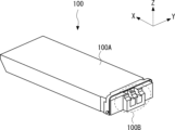
まず、プラガブル光モジュール100の外観について説明する。図1は、実施の形態1にかかるプラガブル光モジュール100を光ファイバの差込側から見た場合の斜視図である。図1に示す符号100Aは、プラガブル光モジュール100の上面を示す。図1に示す符号100Bは、コネクタ付光ファイバのコネクタの差込口を示す。図2は、実施の形態1にかかるプラガブル光モジュール100を光通信装置側から見た場合の斜視図である。図2に示す符号100Cは、プラガブル光モジュール100の下面を示す。図2に示す符号100Dは、外部の光通信装置との接続部を示す。
First, the appearance of the pluggable
続いて、プラガブル光モジュール100の基本的な内部構造について説明する。図3は、実施の形態1にかかるプラガブル光モジュール100の内部構造の一例を模式的に示す斜視図である。図3は、筐体10の下面(図2の符号100C)のカバーを取り外して光通信装置側から見た場合のプラガブル光モジュール100の内部構造を示している。
Next, the basic internal structure of the pluggable
図3に示すように、プラガブル光モジュール100の外形となる筐体10内部には、種々の光部品、プリント回路基板等が設けられる。筐体10内に設けられた光部品は、光ファイバによって光学的に接続される。また、筐体10内部で引き回される光ファイバの余長を収容するための光ファイバ収容手段として、光ファイバ収容部が設けられる。
As shown in FIG. 3 , various optical components, printed circuit boards, and the like are provided inside a
図3の例では、筐体10内部に、プリント回路基板7が収納されている。図示しないが、プリント回路基板7の上面(Z+側の面)には、種々の光部品が実装されてもよい。プリント回路基板7の下方(Z-側)には、光部品5(第1の光部品とも称する)と光部品6(第2の光部品とも称する)とが設けられる。光部品5及び6としては、光源、光変調器、光受信器、プラガブル電気コネクタ、プラガブル光レセプタ、エルビウム添加光ファイバ増幅器(Erbium Doped optical Fiber Amplifier:EDFA)等の各種の光部品が含まれ、かつ、プリント回路基板7に実装される光部品も含まれる。なお、図3の例では、インターフェース部品の具体例として、プラガブル電気コネクタ1及びプラガブル光レセプタ2を表示している。
In the example of FIG. 3, the printed circuit board 7 is housed inside the
光ファイバ収容部3(第1の光ファイバ収容部又は第1の光ファイバ収容手段とも称する)と光ファイバ収容部4(第2の光ファイバ収容部又は第2の光ファイバ収容手段とも称する)とは、プレート状の部材として構成され、筐体10内部の下面側(Z-側の部分)に収納されている。光ファイバ収容部3は、例えば光部品5と他の光部品であるプラガブル光レセプタ2とを接続する光ファイバF1の余長を収納するように設けられる。光ファイバ収容部4は、例えば光部品6と他の光部品であるプラガブル光レセプタ2とを接続する光ファイバF2の余長を収納するように設けられる。
An optical fiber housing portion 3 (also referred to as a first optical fiber housing portion or first optical fiber housing means) and an optical fiber housing portion 4 (also referred to as a second optical fiber housing portion or second optical fiber housing means) is configured as a plate-shaped member and housed on the lower surface side (Z− side portion) inside the
光ファイバ収容部3及び4は、側面の一部が筐体10の内面に接触するように構成され、接触部が筐体10に固定されることで、光ファイバ収容部3及び4の位置が固定される。例えば、光ファイバ収容部3及び4の側面の形状が筐体10の内面に沿って嵌め込み可能な段差構造やくぼみ構造を有しており、当該嵌め込み可能な構造により固定されてもよい。この場合、筐体10側にも光ファイバ収容部3及び4の側面の形状に応じた構造が形成される。また、例えば、光ファイバ収容部3及び4には貫通孔が設けられ、筐体10に設けられたビス穴が設けられ、この貫通孔とビス穴にビスを螺入することで、光ファイバ収容部3及び4を筐体10に固定してもよい。なお、光ファイバ収容部3及び4の固定方法はビスに限られるものではなく、種々の固定方法を用いてもよいことは言うまでもない。
The optical
これにより、光ファイバF1及びF2の余長が、それぞれ光ファイバ収容部3及び4に収容される。よって、光ファイバ収容部3及び4を経由する光ファイバF1及びF2が他の光部品やプリント回路基板7と干渉することを防止でき、その結果、光ファイバF1及びF2の破損を防止できる。なお、以下では、光ファイバF1を第1の光ファイバとも称し、光ファイバF2を第2の光ファイバとも称する。
As a result, the extra lengths of the optical fibers F1 and F2 are accommodated in the optical
この例では、図3に示すように、光ファイバ収容部3及び4は、筐体10内部において、他の光部品や、他の部品が実装されたプリント回路基板7の下方(Z-側)に配置される。この場合、光ファイバ収容部3及び4は、光ファイバ収容部3及び4の光ファイバが収容された面が他の光部品やプリント回路基板7に向かないように配置されることが望ましい。これにより、光ファイバF1及びF2が他の光部品やプリント回路基板7と干渉するのをより確実に避けることができるので、光ファイバF1及びF2の破損をより確実に防止することができる。
In this example, as shown in FIG. 3, the optical
なお、図3は例示に過ぎず、光ファイバの破損が防止できるならば、光ファイバ収容部3及び4の光ファイバが収容される面の向きは、上側(Z+側)でも下側(Z-側)でもよい。また、光ファイバの破損が防止できるならば、プリント回路基板の光部品などが実装される面の向きは、上側(Z+側)でも下側(Z-側)でもよい。
Note that FIG. 3 is only an example, and if damage to the optical fiber can be prevented, the orientation of the surfaces of the optical
図3に示すプラガブル光モジュール100の内部構造は、理解を容易にするために簡略化して示したものであり、この例に限られるものではない。図3では、光部品の例として光部品5及び6を挙げたが、これは例示に過ぎず、筐体10内部には光部品5及び6以外の1又は複数の他の光部品が設けられてもよく、設けられる位置はプリント回路基板7の上側(Z+側)でも下側(Z-側)よい。また、図3では、プリント回路基板の例としてプリント回路基板7を挙げたが、これは例示に過ぎず、筐体10内部にはプリント回路基板7以外の1又は複数の他のプリント回路基板が設けられてもよい。さらに、光ファイバF1及びF2以外にも、筐体10内部の光部品間を接続する1又は複数の光ファイバが設けられてもよい。光ファイバ収容部3は、光ファイバF1だけでなく、光ファイバF1以外の、光ファイバF2を含む1又は複数の他の光ファイバを収容してもよい。光ファイバ収容部4は、光ファイバF2だけでなく、光ファイバF2以外の、光ファイバF1を含む1又は複数の他の光ファイバを収容してもよい。
The internal structure of the pluggable
続いて、光ファイバ収容部3の構成について説明する。図4は、光ファイバ収容部3の構成を模式的に示す斜視図である。光ファイバ収容部3は、プレート状の部材として構成され、プレート部材30上に、光ファイバをガイドするガイドG31及びG32を有する。ガイドG31及びG32は、Y方向を長手方向とし、X方向に並列して配置される。光ファイバは、このガイドG31及びG32の外周に沿って曲げられ、又は、外周に沿って周回することで、光ファイバ収容部3に収容される。
Next, the configuration of the optical
図5は、光ファイバ収容部3の光ファイバの収容態様を示す斜視図である。図5に示すように、ガイドG31及びG32を囲む経路に沿って1回以上周回することで、光ファイバFが収容される。ここで示した光ファイバFは、例えば上述の光ファイバF1、又は、光ファイバF1を含む複数本のファイバの集合体である。なお、光ファイバはガイドG31及びG32を囲む経路を周回する必要はなく、当該経路の一部に沿って曲げられて収容されてもよい。
FIG. 5 is a perspective view showing how the optical fiber is accommodated in the optical
光ファイバFは、周回の径方向及び軸方向において重複するように巻き取られて収容されてもよい。これにより、光ファイバFの周回数を多くすることができるので、光ファイバ収容部3の限定された空間に、多数本のかつ長寸法の光ファイバを効率よく収納することができる。
The optical fiber F may be wound and accommodated so as to overlap in the radial and axial directions of the loop. As a result, since the number of turns of the optical fiber F can be increased, a large number of long optical fibers can be efficiently accommodated in the limited space of the optical
続いて、光ファイバ収容部4の構成について説明する。図6は、光ファイバ収容部4の構成を模式的に示す上面図である。光ファイバ収容部4は、プレート部材40に設けられた、円形ガイドG41及びG42、ガイドG43及びG44を有する。円形ガイドG41及びG42は、それぞれ四角形の対角の位置に設けられる。ガイドG43及びG44は、それぞれ、円形ガイドG41及びG42が設けられた位置とは異なる四角形の対角の位置に設けられる。円形ガイドG41及びG42は、光ファイバを巻き取ることができる。また、光ファイバは、ガイドG43及びG44の曲線部分に沿って曲げられる。
Next, the configuration of the optical
図6に示すように、光ファイバは、円形ガイドG41の外周からガイドG43の曲線部分を経て、円形ガイドG42の外周に到達する経路を通ることが可能である(当然ながら、光ファイバは、この逆方向の経路を通ることも可能である)。光ファイバは、円形ガイドG41の外周からガイドG44の曲線部分を経て、円形ガイドG42の外周に到達する経路を通ることが可能である(当然ながら、光ファイバは、この逆方向の経路を通ることも可能である)。 As shown in FIG. 6, the optical fiber can pass from the outer circumference of the circular guide G41 through the curved portion of the guide G43 to reach the outer circumference of the circular guide G42. It is also possible to go through the reverse path). The optical fiber can pass through a path from the outer circumference of the circular guide G41 through the curved portion of the guide G44 to reach the outer circumference of the circular guide G42 (of course, the optical fiber can pass through this path in the opposite direction). is also possible).
図6に示す光ファイバFは、例えば上述の光ファイバF2、又は、光ファイバF2を含む複数本のファイバの集合体である。粗いハッチング部は、ガイドの上面及びガイドの上面と同じ高さの面を示す。細かいハッチング部は、ガイドの上面よりも低い、光ファイバが通る凹部の底面を示す。 The optical fiber F shown in FIG. 6 is, for example, the above-described optical fiber F2 or an assembly of a plurality of fibers including the optical fiber F2. Coarse hatching indicates the top surface of the guide and the surface level with the top surface of the guide. Fine hatching indicates the bottom surface of the recess through which the optical fiber passes, which is lower than the top surface of the guide.
また、光ファイバを、円形ガイドG42とガイドG43との間を通って、円形ガイドG41及びG42、ガイドG44へ引き回すことができる(当然ながら、光ファイバは、この逆方向の経路を通ることも可能である)。光ファイバを、円形ガイドG42とガイドG43との間を通って、円形ガイドG41及びG42、ガイドG44へ引き回すことができる(当然ながら、光ファイバは、この逆方向の経路を通ることも可能である)。光ファイバを、円形ガイドG41とガイドG44との間を通って、円形ガイドG41及びG42、ガイドG43へ引き回すことができる(当然ながら、光ファイバは、この逆方向の経路を通ることも可能である)。光ファイバを、円形ガイドG42とガイドG43との間を通って、円形ガイドG41及びG42、ガイドG43へ引き回すことができる(当然ながら、光ファイバは、この逆方向の経路を通ることも可能である)。 Also, the optical fiber can be routed between the circular guides G42 and G43 to the circular guides G41 and G42 and to the guide G44 (the optical fiber can of course also pass through this route in the opposite direction. is). An optical fiber can be routed between circular guides G42 and G43, to circular guides G41 and G42, and to guide G44 (of course, the optical fiber can also follow this route in the opposite direction. ). An optical fiber can be routed between circular guides G41 and G44 to circular guides G41 and G42 and guide G43 (of course, the optical fiber can also follow this path in the opposite direction. ). The optical fiber can be routed between the circular guides G42 and G43 to the circular guides G41 and G42 and to the guide G43 (of course, the optical fiber can also follow this path in the opposite direction. ).
また、光ファイバ収容部4は、円形ガイドG41及びG42、ガイドG43及びG44の外周面から外側に突き出した突起41を有する。また、円形ガイドG41及びG42、ガイドG43及び44を囲むように形成された外枠部には、内側に突き出した突起41が設けられる。突起41は、下側に光ファイバが挿通可能に構成される。これにより、たわみやねじれなどにより、巻き取られた光ファイバが光ファイバ収容部4の外部に飛び出すことを防止できる。これにより、光ファイバをより確実に光ファイバ収容部4に収容するとともに、ガイドから光ファイバが外れてしまう事態を防止することができる。なお、光ファイバ収容部3にも同様の突起を設けてもよいことは、いうまでもない。
Further, the optical
また、突起41の下部には、開口部42が設けられてもよい。開口部42の開口幅W1は、突起41の幅W2よりも広いことが望ましい。この場合、突起41で押さえられた光ファイバが下側にたわむことができ、光ファイバの収容が容易となる。また、光ファイバ収容部4の底面と突起41の下面との間の距離が短い場合でも、開口部42を設けることで、光ファイバを挿通させる空間を確保することが可能となる。
Further, an
なお、光ファイバは、開口部42を通って、光ファイバ収容部4の下方に引き出され、又は、光ファイバ収容部4の下方から光ファイバが入って円形ガイドに巻き取られる構成としてもよい。これによれば、光ファイバ収容部4の下方に位置する部品に対する光配線をより容易に行うことができる。よって、光ファイバ収容部4及び他の部品の配置の自由度を高めることが可能となる。
The optical fiber may pass through the
以上、本構成によれば、プラガブル光モジュール100の内部における光配線に用いる光ファイバを他の部品と干渉することなく収容できることが理解できる。なお、光ファイバ収容部3及び4は、例えば、樹脂又は金属によって形成される。
As described above, according to this configuration, it can be understood that the optical fiber used for the optical wiring inside the pluggable
続いて、プラガブル光モジュール100の基本的な構造について説明する。図7は、実施の形態1にかかる光通信システム1000の構成を模式的に示すブロック図である。図7に示すように、プラガブル光モジュール100は、光ファイバF11及びF12の端部に設けられたコネクタ部が挿抜可能に構成される。光ファイバF11及びF12のコネクタとしては、例えばLC型コネクタやMU型コネクタを用いることができる。プラガブル光モジュール100は、通信ホスト装置である光通信装置20から入力される制御信号CONに基づいて制御される。プラガブル光モジュール100は、制御信号CONとともに、光通信装置20からデータ信号である変調信号MODを受信することも可能である。この場合、プラガブル光モジュール100は、受信した変調信号MODに基づいて変調した光信号LS1(第1の光信号とも称する)を、光ファイバF11を介して出力することができる。また、プラガブル光モジュール100は、光ファイバF12を介して外部から受信した光信号LS2(第2の光信号とも称する)を復調したデータ信号DATを、光通信装置へ出力することができる。
Next, the basic structure of the pluggable
光通信装置20は、例えば、プラガブル光モジュール100からの通信データ信号又はプラガブル光モジュール100に入力する通信データ信号のフレーム処理等の通信データ処理を行う。光通信装置20は、例えば、局舎に収容される光伝送装置であり、また、ラックやボックスに挿入されるラインカードのようなものであってもよい。この場合、ラインカードはプラガブル光モジュール100のレセプタを有する。
The optical communication device 20 performs communication data processing such as frame processing of a communication data signal from the pluggable
プラガブル光モジュール100は、プラガブル電気コネクタ1、プラガブル光レセプタ2、光ファイバ収容部3及び4、制御部11、光源12、分岐部13、変調器14、受信器15、エルビウム添加光ファイバ増幅器(EDFA:Erbium Doped optical Fiber Amplifier)16、励起光源17及び光減衰器18を有する。
The pluggable
プラガブル電気コネクタ1は、光通信装置20に挿抜可能なI/O(Input/Output)ポートとして構成される。光通信装置20からは、プラガブル電気コネクタ1を介して、電気信号である制御信号CONが制御部11へ出力され、電気信号である変調信号MODが変調器14へ出力される。また、受信器15からは、プラガブル電気コネクタ1を介して、データ信号DATが光通信装置20へ出力される。
The pluggable electrical connector 1 is configured as an I/O (Input/Output) port that can be inserted into and removed from the optical communication device 20 . From the optical communication device 20 , a control signal CON, which is an electrical signal, is output to the
プラガブル光レセプタ2は、光ファイバF11及びF12のコネクタが挿抜可能に構成される。光信号LS1は、プラガブル光レセプタ2を介して、光ファイバF11に送出される。光ファイバF12を伝搬してプラガブル光モジュール100に入力される光信号LS2は、プラガブル光レセプタ2を介して、受信器15に入力される。なお、プラガブル光レセプタ2を単一の部品として説明したが、当然のことながら、光ファイバF11が挿抜可能なプラガブル光レセプタと光ファイバF12が挿抜可能なプラガブル光レセプタとが分離して設けられてもよい。
The pluggable
制御部11は、制御信号CONに応じて、プラガブル光モジュール100の各部、すなわち、光源12、変調器14、受信器15、励起光源17及び光減衰器18の動作を制御可能に構成される。この例では、制御部11は、制御信号CONに応じて制御信号CON1~CON5を生成し、制御信号CON1~CON5を、例えばプラガブル電気コネクタ1を介して、それぞれ光源12、変調器14、受信器15、励起光源17及び光減衰器18へ出力する。
The
光源12は、制御信号CON1に応じて決定された波長の光を出力する波長可変光源(例えば、ITLA:Integrated Tunable Laser Assembly)として構成される。光源12は、例えば、半導体光増幅器と波長フィルタとを有する光源ユニットとして構成してもよい。
The
分岐部13は、光源12が出力した光L1を、光L2と局部発振光LOとに分岐する。分岐部13としては、Y分岐、ビームスプリッタ、プリズムなどの入射する光を分岐できる各種の光学部品を用いてもよい。
The
変調器14は、光通信装置20からプラガブル電気コネクタ1を介して入力される変調信号MODに基づいて、分岐部13で分岐された光L2を変調し、変調光を光信号LS1として出力する。変調器14の動作は、制御部11から入力される制御信号CON2に基づいて制御される。これにより、変調器14は、光L2の波長に応じた適切な変調動作を行うことができる。
The
変調器14は、例えばマッハツェンダ光変調器として構成してもよい。変調器14をマッハツェンダ光変調器として構成した場合、マッハツェンダ光変調器の光導波路に設けられた位相変調領域に変調信号MODに応じた信号を印加することで、光L2を変調することができる。変調器14は、位相変調、振幅変調、偏波変調などの各種の変調方式で、又は、各種の変調方式を組み合わせて光L2を変調することができる。ここで、マッハツェンダ型光変調器は、例えば、半導体光変調器等である。
上述の位相変調領域とは、光導波路上に形成された電極を有する領域である。位相変調領域の電極に電気信号、例えば電圧信号が印加されることにより、電極下の光導波路の実効屈折率が変化する。その結果、位相変調領域の光導波路の実質的な光路長を変化させることができる。これにより、位相変調領域の光導波路を伝搬する光信号の位相を変化させることができる。マッハツェンダ変調器では、2本の光導波路の間を伝搬する光信号間に位相差を与えて、その後2つの光信号を合波することで、合波後の光信号を変調することができる。 The phase modulation region described above is a region having electrodes formed on the optical waveguide. By applying an electric signal, eg, a voltage signal, to the electrodes in the phase modulation region, the effective refractive index of the optical waveguide under the electrodes changes. As a result, the substantial optical path length of the optical waveguide in the phase modulation region can be changed. Thereby, the phase of the optical signal propagating through the optical waveguide of the phase modulation region can be changed. In the Mach-Zehnder modulator, by giving a phase difference between optical signals propagating between two optical waveguides and then combining the two optical signals, the combined optical signal can be modulated.
受信器15は、例えば、DP-QPSK(Dual-Polarization Quadrature Phase-Shift Keying)光信号を電気信号に復調するデジタルコヒーレント受信を行う受信器(例えば、ICR:Integrated Coherent Receiver)として構成される。受信器15は、光ファイバF12を介して外部から受信した光信号LS2を、局部発振光LOと干渉させることで復調を行う。受信器15は、復調された電気信号であるデータ信号DATを、プラガブル電気コネクタ1を介して光通信装置20へ出力する。受信器15は、制御部11が出力する制御信号CON3によって制御され、光信号LS2(ないしは局部発振光LO)の波長に応じた最適な復調動作を行うことができる。
The
EDFA16は、ファイバ型光増幅器であり、変調器14から出力された光信号LS1を増幅し、増幅した光信号LS1を出力する。
The
励起光源17は、EDFA16を励起するための励起光Leを、EDFA16へ出力する。励起光源17の動作は、制御部11が出力する制御信号CON4によって制御される。
The
光減衰器18(第1の光減衰器とも称する)は、光信号LS1を減衰させる可変光減衰器(VOA:Variable Optical Attenuator)として構成される。この可変光減衰器(VOA)は、例えば利得制御によって出力する光のパワーを制御可能な半導体光増幅器(Semiconductor Optical Amplifier)や物理的に光を遮るシャッターなどで実現されてもよい。換言すれば、ここでいう光減衰器18とは、上述の半導体光増幅器やシャッターなどの、出力する光のパワーを制御する又は遮ることができる光パワー調整部として機能し得る各種の光学部品を含む。これにより、光信号LS1の光強度(光パワー)を所望の値に調整することができる。光減衰器18の動作は、制御部11が出力する制御信号CON5によって制御される。光減衰器18を通過した光信号LS1は、プラガブル光レセプタ2を介して光ファイバF12に出力される。
The optical attenuator 18 (also referred to as a first optical attenuator) is configured as a variable optical attenuator (VOA) that attenuates the optical signal LS1. This variable optical attenuator (VOA) may be implemented by, for example, a semiconductor optical amplifier capable of controlling the power of output light by gain control, or a shutter that physically blocks light. In other words, the
光ファイバ収容部3は、プラガブル光レセプタ2と光減衰器18との間を接続する光ファイバF1を収容するように構成される。つまり、光減衰器18は、上述の光部品5に対応している。
The optical
光ファイバ収容部4は、プラガブル光レセプタ2と受信器15との間を接続する光ファイバF2を収容するように構成される。つまり、受信器15は、上述の光部品6に対応している。
The optical
一般に、デジタルコヒーレント光通信の用に供するプラガブル光モジュールでは、上述の通り、筐体10の内部に複数の光部品を搭載する必要があるだけでなく、プラガブル光モジュールの寸法の小型化が強く求められる。そのため、比較的狭小な筐体に複数の部品を収め、かつ、必要に応じて、光ファイバを用いて部品間を接続する必要がある。しかし、部品の取り付け位置のばらつきや、光ファイバの切断長さのばらつきなどで、最適な長さ光ファイバを用途ごとに準備することは困難であり、実現できたとしても工数の増大を招くこととなる。しかし、本構成によれば、要求される長さに対して、余裕のある長さの光ファイバを用いて光部品間を接続するとともに、光ファイバ収容部によって光ファイバの余長を収容できる。これにより、部品の取り付けばらつきやファイバの切断バラつきなどの影響を受けることなく、容易にプラガブル光モジュール内で光ファイバを用いた光配線を行うことができる。
In general, a pluggable optical module used for digital coherent optical communication not only requires a plurality of optical components to be mounted inside the
また、本構成では、プラガブル光モジュール内で用いる光ファイバの長さに余裕が有るので、光ファイバ収容部を介して光ファイバを取り回す場合に、光ファイバに不要な緊張(テンション)が加わることを防止できる。これにより、プラガブル光モジュール作製工程における光ファイバの破損を防止できるので、製造歩留まり向上の観点から有利であることが理解できる。 In addition, in this configuration, the length of the optical fiber used in the pluggable optical module has a margin, so that unnecessary tension is not applied to the optical fiber when the optical fiber is routed through the optical fiber housing section. can be prevented. As a result, it is possible to prevent the optical fiber from being damaged in the pluggable optical module manufacturing process, so it can be understood that this is advantageous from the viewpoint of improving the manufacturing yield.
また、本構成によれば、光ファイバ収容部が他の部品と干渉することもなく、かつ、収容された位置からずれたりすることもないので、収容後の光ファイバが他の部品と接触して破損するといった事態も防止することができる。これにより、プラガブル光モジュールを他の装置に挿抜するときの振動や衝撃が生じても光ファイバは破損しないので、運用中のプラガブル光モジュール100の故障を防止する観点から有利であることが理解できる。 In addition, according to this configuration, the optical fiber accommodating portion does not interfere with other parts and does not shift from the accommodated position, so that the optical fiber after being accommodated does not come into contact with other parts. It is also possible to prevent a situation in which the device is damaged. As a result, the optical fiber will not be damaged even if vibration or impact occurs when the pluggable optical module is inserted into or removed from another device. .
また、本構成では、プレート状の光ファイバ収容部内に光ファイバを環状に収容できるため、光ファイバ収容部の厚みを抑制することができる。よって、筐体内の狭小な空間に光ファイバ収容部を設けることができる。したがって、プラガブル光モジュールの小型化の観点から有利であることが理解できる。 Further, in this configuration, since the optical fibers can be annularly accommodated in the plate-shaped optical fiber accommodating portion, the thickness of the optical fiber accommodating portion can be suppressed. Therefore, the optical fiber accommodating portion can be provided in a narrow space inside the housing. Therefore, it can be understood that it is advantageous from the viewpoint of miniaturization of the pluggable optical module.
本実施の形態では、光ファイバ収容部を2つ設ける例について説明したが、3つ以上の光ファイバ収容部を設けてもよい。このように、光ファイバ収容部を複数設けることで、プラガブル光モジュール100の筐体内の光部品の配置又は数を変更する場合でも、複数の光ファイバ収容部のうち、一部の光ファイバ収容部の設計を変更するのみで対応することができる。これにより、プラガブル光モジュールの設計変更に対する柔軟性を確保でき、かつ、プラガブル光モジュールの他品種化に対応できる点で有利である。
In this embodiment, an example in which two optical fiber accommodation units are provided has been described, but three or more optical fiber accommodation units may be provided. By providing a plurality of optical fiber housing units in this way, even when the arrangement or the number of optical components in the housing of the pluggable
例えば、プラガブル光モジュールの設計変更によって筐体内の光部品の配置又は数を変更する場合、変更が必要な光ファイバ収容部のみを交換すればよく、製造工程の変更を小さくすることができる。 For example, when the arrangement or number of optical components in the housing is changed due to a design change of the pluggable optical module, only the optical fiber accommodating portion that needs to be changed needs to be replaced, and the change in the manufacturing process can be reduced.
また、プラガブル光モジュールを他品種化した場合、筐体内の光部品の配置は、品種間で共通する部分と、品種間で異なる部分とが存在することが想定される。この場合、共通部分の光配線に用いる光ファイバの収容には共通の光ファイバ収容部を用い、異なる部分の光配線に用いる光ファイバの収容には、それぞれ異なる形状を有する光ファイバ収容部を用いればよい。これにより、品種間における工程の相違を最小化することができるので、リードタイムの短縮や製造コストの抑制を実現できる。 In addition, when the pluggable optical modules are of different types, it is assumed that the arrangement of the optical components in the housing will have a portion common to the types and a portion different from the types. In this case, a common optical fiber accommodating portion is used to accommodate the optical fibers used for the optical wiring of the common portion, and optical fiber accommodating portions having different shapes are used to accommodate the optical fibers used for the optical wiring of the different portions. Just do it. As a result, it is possible to minimize the difference in the process between product types, thereby shortening the lead time and suppressing the manufacturing cost.
加えて、光ファイバ収容部による光ファイバの収容が伴う光部品間の光配線作業を、光ファイバ収容部ごとに分けて並行して行うことが可能となるので、光配線作業に要する時間を低減することも可能となる。 In addition, the optical wiring work between optical components, which entails the accommodation of the optical fibers in the optical fiber accommodation units, can be divided for each optical fiber accommodation unit and performed in parallel, thereby reducing the time required for the optical wiring work. It is also possible to
実施の形態2
実施の形態2にかかるプラガブル光モジュール200について説明する。実施の形態2にかかるプラガブル光モジュール200は、実施の形態1にかかるプラガブル光モジュール100の変形例であり、光ファイバ収容部3にEDFA16を構成する光ファイバ(EDF)が収容されている。
A pluggable
図8は、実施の形態2にかかるプラガブル光モジュール200の構成を模式的に示すブロック図である。プラガブル光モジュール200は、EDFA16を構成するEDFが、光ファイバ収容部3に収容される。プラガブル光モジュール200のその他の構成は、プラガブル光モジュール100と同様であるので説明を省略する。
FIG. 8 is a block diagram schematically showing the configuration of the pluggable
デジタルコヒーレント通信に供されるプラガブル光モジュールは、図7に示したように、出力する光信号LS1の光出力を確保するために、EDFAが実装される場合がある。このため、EDFA及びEDFAへ励起光を入力する励起光源の追加により、プラガブル光モジュールの筐体内での光部品実装はより高密度化する。さらに、EDFAは、一般に、数mないし数十m程度のEDFを有する。そのため、プラガブル光モジュールでは、長寸法のEDFを筐体内に他の光部品などと干渉することなく収める必要がある。 As shown in FIG. 7, a pluggable optical module used for digital coherent communication may be equipped with an EDFA in order to secure the optical output of the output optical signal LS1. Therefore, by adding an EDFA and an excitation light source for inputting excitation light to the EDFA, optical components can be mounted more densely in the housing of the pluggable optical module. Furthermore, the EDFA generally has an EDF of several meters to several tens of meters. Therefore, in a pluggable optical module, it is necessary to accommodate a long EDF in a housing without interfering with other optical components.
これに対し、本構成では、光ファイバ収容部3でEDFを複数回周回させることで、EDFを光ファイバ収容部3にコンパクトに収納することができる。この際、EDFを予め定められた寸法、形状で巻き取り、巻き取ったEDFを光ファイバ収容部にはめ込むことで、EDFを容易に収納できる。これにより、EDFAを用いる場合でも、EDFAを構成するEDFの破損を防止しつつ、EDFAをプラガブル光モジュール内にコンパクトに収容できることが理解できる。
On the other hand, in the present configuration, the EDF can be compactly housed in the optical
実施の形態3
実施の形態3にかかるプラガブル光モジュール300について説明する。プラガブル光モジュール300は、実施の形態2にかかるプラガブル光モジュール200の光ファイバ収容部3を光ファイバ収容部8に置換した構成を有する。以下、光ファイバ収容部8について説明する。
A pluggable optical module 300 according to the third embodiment will be described. The pluggable optical module 300 has a configuration in which the optical
図9は、実施の形態3にかかる光ファイバ収容部8の構成を模式的に示す斜視図である。光ファイバ収容部8は、光ファイバ収容部3にスプライス収納部8Aを追加した構成を有する。図10は、実施の形態3にかかる光ファイバ収容部8の光ファイバの収容態様を示す斜視図である。本実施の形態では、光ファイバFが収容される空間の下に、スプライス収納部8Aが設けられている。
FIG. 9 is a perspective view schematically showing the configuration of the optical
光ファイバFは、2本の光ファイバを接合した部分にスプライス部SPが設けられる。スプライス部SPは、一般に、2本のファイバの接合部を補強スリーブで覆うことで補強されている。スプライス収納部8Aは、例えばスプライス部SPのスリーブをはめ込む溝が設けられる。図9及び10に示すように、Y方向に延在する溝にスプライス部SPをはめ込むことで、スプライス部SPを固定することができる。
The optical fiber F is provided with a splice portion SP at a portion where two optical fibers are spliced. The splice SP is typically reinforced by covering the junction of the two fibers with a reinforcing sleeve. The
一般に、スプライス部を有する光ファイバでは、スプライス部のファイバ接合部は他の部位と比べて引っ張りや曲げに対する機械的強度が小さくなってしまう。そこで、本構成では、スプライス収納部8Aによってスプライス部SPを固定することで、光ファイバに力がかかった場合のスプライス部SPの動きを抑制し、光ファイバ接合部にかかる負担を軽減できる。その結果、光ファイバの引き回し、光ファイバ収容部の取り付けなどの際に光ファイバに力が加わっても、光ファイバの断線を防止することが可能となる。
In general, in an optical fiber having a splice, the fiber joint portion of the splice has less mechanical strength against tension and bending than other portions. Therefore, in this configuration, by fixing the splice part SP by the
スプライス部は、光ファイバの整合部分を所定の長さにわたって保護するものである。そのため、スプライス収納部は、スプライス部を収納するに足る長さを有する必要がある。本実施の形態にかかる光ファイバ収容部8は、所定の曲率以上の曲率で複数回周回する光ファイバFを収容するための面積をX-Y平面において有している。これを利用して、光ファイバFとスプライス部SPとが、光ファイバFの周回の軸方向(Z方向)に積層されるようにスプライス収納部8Aを設けることで、光ファイバ収容部8のX-Y平面における面積を増加させることなくスプライス部を収納できる。よって、本構成によれば、プラガブル光モジュールの小型を実現しつつ、光ファイバ収容部にスプライス部を収納することができる。
The splice protects the mating portion of the optical fiber over a length. Therefore, the splice housing must be long enough to accommodate the splice. The optical
上述では、スプライス収納部8Aが延在する方向、すなわち長手方向をY方向としたが、スプライス収納部8Aの長手方向はX方向でもよく、X-Y平面に平行な任意の方向(すなわち、光ファイバFの周回の軸方向に垂直な平面に対して平行な方向)としてもよい。また、長手方向が同じ、又は、長手方向が異なる複数のスプライス収納部を設けてもよい。また、スプライス収納部が許容できるならば、任意の個数のスプライス部をスプライス収納部に収納してもよい。
In the above description, the direction in which the
以下、スプライス収納部の配置例について説明する。図11は、光ファイバ収容部8の変形例である光ファイバ収容部81の構成を模式的に示す斜視図である。光ファイバ収容部8ではスプライス収納部8AがY方向に延在し、Y方向を長手方向とするスプライス部SPが光ファイバ収容部8に収納されていた。これに対し、図11の光ファイバ収容部81では、スプライス収納部8Aに代えて、X方向に延在するスプライス収納部8Bが光ファイバFの周回の軸方向(Z方向)に積層されるように設けられている。そして、X方向を長手方向とするスプライス部SPが光ファイバ収容部81に収納される。よって、スプライス収納部の長手方向がX方向の場合でも、図9及び図10の例と同様に、光ファイバ収容部81のX-Y平面における面積を増加させることなくスプライス部を収納できる。
An example of arrangement of the splice housing will be described below. FIG. 11 is a perspective view schematically showing the configuration of an optical
図12は、光ファイバ収容部8の変形例である光ファイバ収容部82の構成を模式的に示す斜視図である。図12に示すように、光ファイバ収容部82では、図9及び図10に示すスプライス収納部8Aと図11に示すスプライス収納部8Bとが、光ファイバFの周回の軸方向(Z方向)に積層されるように設けられている。よって、光ファイバ収容部82のX-Y平面における面積を増加させることなく、より多くのスプライス部を収納することが可能となる。
FIG. 12 is a perspective view schematically showing the configuration of an optical
上述では、スプライス収納部にスプライス部が収納されるものとして説明したが、光ファイバの接合部は例えばコネクタなどの他の接続方法によって接続された光ファイバの接続部が収納されてもよい。換言すれば、スプライス収納部を含む接続部の収納部に、任意の接続方法で接続された光ファイバの接続部が収納されてもよい。 In the above description, the splice portion is housed in the splice housing portion, but the splice portion of the optical fiber may house the splice portion of the optical fiber connected by another connection method such as a connector. In other words, the splicing portion of the optical fiber spliced by any splicing method may be accommodated in the splicing portion accommodating portion including the splice accommodating portion.
さらに、本実施の形態では、光ファイバ収容部8にスプライス収納部8Aが設けられるもとして説明したが、光ファイバ収容部4を含む他の光ファイバ収容部に同様のスプライス収納部を設けてもよい。
Furthermore, in the present embodiment, the
実施の形態4
実施の形態4にかかるプラガブル光モジュール400について説明する。プラガブル光モジュール400は、実施の形態1にかかるプラガブル光モジュール100の変形例であり、光ファイバ収容部3及び4の他にも、筐体10内部の光ファイバをガイドするための構成が追加されている。
A pluggable
図13は、実施の形態4にかかるプラガブル光モジュール400の内部構造を模式的に示す斜視図である。図13に示すように、プラガブル光モジュール400では、光部品6が筐体10内部の上側(Z+側)に設けられている。光部品6と光ファイバ収容部4との間を結ぶ光ファイバF2は、筐体10に固定されたガイド治具10Aのスロープに設けられた溝に沿って引き回される。これにより、縦方向(Z方向)において高低差がある光部品6と光ファイバ収容部4との間を結ぶ光ファイバを許容範囲内の曲率で曲げつつガイドすることができる。また、光ファイバF2は、ガイド治具10Aの溝によって位置が固定されるので、光ファイバF2が他の光部品等に干渉して破損することを防止することができる。
FIG. 13 is a perspective view schematically showing the internal structure of the pluggable
また、筐体10内部の上側(Z+側)には、光ファイバ収容部4から延びる光ファイバF3をガイドするための溝10Bが設けられている。なお、溝10Bは、ガイド治具10Aと同様に、ガイド治具の一例である。これにより、光ファイバF3を許容範囲内の曲率で曲げつつガイドすることができる。また、光ファイバF3は、溝10Bによって位置が固定されるので、光ファイバF3が他の光部品等に干渉して破損することを防止することができる。
Further, a
なお、ガイド治具10Aは、筐体10に固定可能な筐体10と物理的に分離した部材として構成されてもよいし、筐体10の一部分として構成されてもよい。溝10Bは、筐体10に形成されてもよいし、筐体10に固定可能な筐体10と物理的に分離した部材に形成された溝であってもよい。さらに、ガイド治具10A及び溝10Bが形成されたガイド治具は、光ファイバ収容部3及び4の一方又は両方に固定可能に構成されてもよい。
The
上述では、ガイド治具10Aと溝10Bとは1つずつ設けられているが、任意のガイド治具が2つ以上設けられてもよく、溝も2本以上設けられてもよい。また、ガイド治具を複数設ける場合、ガイドされる光ファイバの曲率は同じであってもよいし、異なっていてもよい。また、溝を複数設ける場合、ガイドされる光ファイバの曲率は同じであってもよいし、異なっていてもよい。
In the above description, one
さらに、ガイド治具10Aと同様の構造及び溝10Bと同様の構造が、光ファイバ収容部3及び4、プリント回路基板7などの他の部品に設けられてもよいことは言うまでもない。
Further, it goes without saying that structures similar to the
次いで、プラガブル光モジュール400の変形例について説明する。図14は、実施の形態4にかかるプラガブル光モジュールの400の変形例であるプラガブル光モジュールの401の内部構造を模式的に示す斜視図である。プラガブル光モジュールの401では、光部品6が実装治具9に搭載されている。
Next, a modified example of the pluggable
光部品6が搭載された実装治具9は、一部がガイド治具と嵌合可能に構成されている。具体的には、ガイド治具10Aから実装治具9へ向けてX方向に沿って延在する突出部10Cには、Z方向に延在するピン10Dが設けられている。実装治具9には、ピン10Dが挿通可能な孔が設けられている。ピン10Dが実装治具9の孔に挿通されることで、実装治具9とガイド治具10Aとの間の相対的な位置が固定される。
A part of the mounting jig 9 on which the
これにより、光部品6と光ファイバ収容部4との間の光ファイバF2の位置が固定されるので、光ファイバF2が他の光部品等に干渉して破損することをより確実に防止することができる。
As a result, the position of the optical fiber F2 between the
その他の実施の形態
なお、本発明は上記実施の形態に限られたものではなく、趣旨を逸脱しない範囲で適宜変更することが可能である。例えば、光ファイバ収容部は、例えば、熱伝導性が高い材料で構成されることが望ましい。この場合、光ファイバ収容部の近傍に実装される他の部品やプリント回路基板の放熱に寄与することができるので、放熱性能の向上を実現することができる。これにより、回路の熱暴走を抑止することができる。
Other Embodiments The present invention is not limited to the above-described embodiments, and can be modified as appropriate without departing from the scope of the invention. For example, it is desirable that the optical fiber housing section be made of a material with high thermal conductivity. In this case, it is possible to contribute to the heat dissipation of other components and the printed circuit board mounted in the vicinity of the optical fiber accommodating portion, so that it is possible to improve the heat dissipation performance. Thereby, thermal runaway of the circuit can be suppressed.
上述の実施の形態で参照した図においては、プラガブル光モジュールに設けられた構成要素間、及び、光通信システムに設けられた構成要素(プラガブル光モジュール及び光通信装置)間での信号伝達を矢印で表したが、これは2つの構成要素間で一方向のみに信号が伝達されることを意味するものではなく、適宜双方向の信号のやり取りが可能であることは言うまでもない。 In the figures referred to in the above embodiments, arrows indicate signal transmission between components provided in the pluggable optical module and between components provided in the optical communication system (pluggable optical module and optical communication device). However, this does not mean that signals are transmitted only in one direction between the two components, and needless to say, bidirectional signal exchange is possible as appropriate.
上述の実施の形態において、変調器への戻り光を防止するため、変調器とEDFAとの間にアイソレータが挿入されてもよい。 In the above embodiments, an isolator may be inserted between the modulator and the EDFA to prevent light from returning to the modulator.
分岐部13は、光源12、変調器14及び受信器15から独立したものとして説明したが、これは例示に過ぎない。例えば、分岐部13は、光源12に組み込まれていてもよい。また、分岐部13は、変調器14に組み込まれていてもよい。この場合、光L1は変調器14に入力され、変調器14内部の分岐部13で分岐され、分岐された局部発振光LOが受信器15に入力される。更に、分岐部13は、受信器15に組み込まれていてもよい。この場合、光L1は受信器15に入力され、受信器15内部の分岐部13で分岐され、分岐された光L2が変調器14に入力される。
Although
上述の実施の形態においては、制御部11は、光通信装置20からの制御信号CONに応じて、光源、光変調器、受信器、励起光源及び光減衰器が制御される例についても説明したが、外部からの制御信号によらず、自律的に光源、光変調器、受信器、励起光源及び光減衰器を制御することもできる。
In the above embodiment, the
上述の実施の形態において、プラガブル電気コネクタ1を介した制御信号のやり取りは、MDIO(Management Data Input/Output)やI2C(Inter-Integrated Circuit)といった技術を適用することで実現することができる。 In the above embodiment, the exchange of control signals via the pluggable electrical connector 1 can be realized by applying techniques such as MDIO (Management Data Input/Output) and I2C (Inter-Integrated Circuit).
上述の実施の形態においては、受信器15は、DP-QPSK光信号を受信するものとして説明したが、これは例示に過ぎない。例えば、QAM(quadrature amplitude modulation)等の他の変調信号を受信可能に構成されてもよい。
In the above embodiment,
上述の実施の形態においては、光源12を半導体光増幅器と波長フィルタとで構成するものとして説明したが、波長可変光源として機能するならば他の構成とすることができる。例えば、光源12は、DFB(Distributed FeedBack)レーザアレイと、DFBレーザアレイに含まれる複数のDFBレーザからのレーザ光を選択する選択部とで構成されてもよい。また、DFB(Distributed FeedBack)レーザアレイに代えて、DBR(Distributed Bragg Reflector)レーザなどの他の種類のレーザで構成されるレーザアレイを用いてもよい。
In the above-described embodiment, the
以上、実施の形態を参照して本願発明を説明したが、本願発明は上記によって限定されるものではない。本願発明の構成や詳細には、発明のスコープ内で当業者が理解し得る様々な変更をすることができる。 Although the present invention has been described with reference to the embodiments, the present invention is not limited to the above. Various changes that can be understood by those skilled in the art can be made to the configuration and details of the present invention within the scope of the invention.
この出願は、2017年8月29日に出願された日本出願特願2017-164625を基礎とする優先権を主張し、その開示の全てをここに取り込む。 This application claims priority based on Japanese Patent Application No. 2017-164625 filed on August 29, 2017, and the entire disclosure thereof is incorporated herein.
CON、CON1-CON5 制御信号
DAT データ信号
F、F1-F3、F11、F12 光ファイバ
G31、G32、G43、G44 ガイド
G41、G42 円形ガイド
L1、L2 光
LO 局部発振光
LS1、LS2 光信号
Le 励起光
MOD 変調信号
SP スプライス部
1 プラガブル電気コネクタ
2 プラガブル光レセプタ
3、4、8、81、82 光ファイバ収容部
5、6 光部品
7 プリント回路基板
8A、8B スプライス収納部
9 実装治具
10 筐体
10A ガイド治具
10B 溝
10C 突出部
10D ピン
11 制御部
12 光源
13 分岐部
14 変調器
15 受信器
16 EDFA
17 励起光源
18 光減衰器
20 光通信装置
30、40 プレート部材
41 突起
42 開口部
100、200、300、400 プラガブル光モジュール
CON, CON1-CON5 Control signal DAT Data signal F, F1-F3, F11, F12 Optical fiber G31, G32, G43, G44 Guide
G41, G42 Circular guides L1, L2 Light LO Local oscillation light LS1, LS2 Optical signal Le Pumping light MOD Modulation signal SP Splice part 1 Pluggable
17
Claims (22)
外部光ファイバと接続可能なプラガブル光レセプタと、
前記プラガブル電気コネクタを介して入力する変調信号に基づいて第1の光信号を出力する変調器と、
前記プラガブル光レセプタを介して入力する第2の光信号に基づいてデータ信号を出力する受信器と、
前記出力された第1の光信号を増幅するファイバ型光増幅器と、
前記ファイバ型光増幅器を構成する第1の光ファイバと、
前記プラガブル光レセプタと前記受信器とを接続する第2の光ファイバと、
前記第1の光ファイバを第1の周回経路に周回させることで、前記第1の光ファイバを収容する第1の光ファイバ収容手段と、
前記第2の光ファイバを第2の周回経路に周回させることで、前記第2の光ファイバを収容する第2の光ファイバ収容手段と、を備え、
前記第1の周回経路の径は、前記第2の周回経路の径よりも長い、
プラガブル光モジュール。 a pluggable electrical connector connectable to an optical transmission device;
a pluggable optical receptor connectable to an external optical fiber;
a modulator that outputs a first optical signal based on a modulated signal that is input via the pluggable electrical connector;
a receiver that outputs a data signal based on a second optical signal input via the pluggable optical receptor;
a fiber type optical amplifier that amplifies the output first optical signal;
a first optical fiber constituting the fiber-type optical amplifier;
a second optical fiber connecting the pluggable optical receptor and the receiver;
a first optical fiber housing means for housing the first optical fiber by winding the first optical fiber along a first winding path ;
a second optical fiber housing means for housing the second optical fiber by winding the second optical fiber along a second winding path ;
The diameter of the first circuit path is longer than the diameter of the second circuit path,
Pluggable optical module.
前記光ファイバ収容手段は、前記収容される光ファイバに設けられた接続部を収納する、前記所定の方向を長手方向とする収納部を備える、
請求項1に記載のプラガブル光モジュール。 One or both of the first optical fiber accommodation means and the second optical fiber accommodation means are configured to accommodate an excess length of the accommodated optical fiber with a predetermined direction as a longitudinal direction. is a means,
The optical fiber housing means includes a housing having the predetermined direction as a longitudinal direction, which houses the connecting portion provided in the optical fiber to be housed.
The pluggable optical module according to claim 1.
前記収納部は、前記収容される光ファイバに対して、周回の軸方向に重なるように設けられる、
請求項2に記載のプラガブル光モジュール。 The optical fiber accommodation means is configured to accommodate the optical fiber by making one or more laps along a predetermined path,
The storage section is provided so as to overlap the optical fiber to be housed in the axial direction of the winding.
3. The pluggable optical module according to claim 2.
請求項2又は3に記載のプラガブル光モジュール。 The storage section is configured to extend in a direction parallel to a plane perpendicular to the axial direction of the winding of the optical fiber to be accommodated,
4. The pluggable optical module according to claim 2 or 3.
請求項1乃至4のいずれか一項に記載のプラガブル光モジュール。 one or both of the first optical fiber housing means and the second optical fiber housing means are in contact with a housing housing the first optical fiber housing means and the second optical fiber housing means, and , the contact portion is fixed to the housing;
The pluggable optical module according to any one of claims 1 to 4.
請求項5に記載のプラガブル光モジュール。 The first optical fiber housing means and the second optical fiber housing means are arranged in the housing such that the surface in which the optical fibers are housed does not face the optical component provided in the housing.
The pluggable optical module according to claim 5.
請求項6に記載のプラガブル光モジュール。 further comprising a guide jig for guiding the optical fiber routed inside the housing,
The pluggable optical module according to claim 6.
請求項7に記載のプラガブル光モジュール。 The guide jig is configured to be physically fixable to one or both of the first optical fiber housing means and the second optical fiber housing means,
The pluggable optical module according to claim 7.
請求項7又は8に記載のプラガブル光モジュール。 The guide jig is configured as a member physically separated from the housing that can be fixed to the housing, or is configured integrally with the housing as part of the housing.
The pluggable optical module according to claim 7 or 8.
請求項2乃至9のいずれか一項に記載のプラガブル光モジュール。 The first and second optical fiber accommodation means are configured so that the optical fiber to be accommodated is bent along a predetermined path and accommodated.
10. The pluggable optical module according to any one of claims 2-9.
請求項10に記載のプラガブル光モジュール。 The first and second optical fiber accommodation means are configured so that the optical fiber to be accommodated is accommodated by making one or more laps along a predetermined path.
The pluggable optical module according to claim 10.
前記プラガブル光モジュールが挿抜可能に構成される光伝送装置と、を備え、
前記プラガブル光モジュールは、
前記光伝送装置と接続可能なプラガブル電気コネクタと、
外部光ファイバと接続可能なプラガブル光レセプタと、
前記プラガブル電気コネクタを介して入力する変調信号に基づいて第1の光信号を出力する変調器と、
前記プラガブル光レセプタを介して入力する第2の光信号に基づいてデータ信号を出力する受信器と、
前記出力された第1の光信号を増幅するファイバ型光増幅器と、
前記ファイバ型光増幅器を構成する第1の光ファイバと、
前記プラガブル光レセプタと前記受信器とを接続する第2の光ファイバと、
前記第1の光ファイバを第1の周回経路に周回させることで、前記第1の光ファイバを収容する第1の光ファイバ収容手段と、
前記第2の光ファイバを第2の周回経路に周回させることで、前記第2の光ファイバを収容する第2の光ファイバ収容手段と、を備え、
前記第1の周回経路の径は、前記第2の周回経路の径よりも長い、
光通信システム。 a pluggable optical module configured to be able to insert and remove an optical fiber and capable of transmitting and receiving an optical signal via the optical fiber;
an optical transmission device configured such that the pluggable optical module can be inserted and removed,
The pluggable optical module is
a pluggable electrical connector connectable to the optical transmission device;
a pluggable optical receptor connectable to an external optical fiber;
a modulator that outputs a first optical signal based on a modulated signal that is input via the pluggable electrical connector;
a receiver that outputs a data signal based on a second optical signal input via the pluggable optical receptor;
a fiber type optical amplifier that amplifies the output first optical signal;
a first optical fiber constituting the fiber-type optical amplifier;
a second optical fiber connecting the pluggable optical receptor and the receiver;
a first optical fiber housing means for housing the first optical fiber by winding the first optical fiber along a first winding path ;
a second optical fiber housing means for housing the second optical fiber by winding the second optical fiber along a second winding path ;
The diameter of the first circuit path is longer than the diameter of the second circuit path,
Optical communication system.
前記光ファイバ収容手段は、前記収容される光ファイバに設けられた接続部を収納する、前記所定の方向を長手方向とする収納部を備える、
請求項12に記載の光通信システム。 One or both of the first optical fiber accommodation means and the second optical fiber accommodation means are configured to accommodate an excess length of the accommodated optical fiber with a predetermined direction as a longitudinal direction. is a means,
The optical fiber housing means includes a housing having the predetermined direction as a longitudinal direction, which houses the connecting portion provided in the optical fiber to be housed.
An optical communication system according to claim 12.
前記収納部は、前記収容される光ファイバに対して、周回の軸方向に重なるように設けられる、
請求項13に記載の光通信システム。 The optical fiber accommodation means is configured to accommodate the optical fiber by making one or more laps along a predetermined path,
The storage section is provided so as to overlap the optical fiber to be housed in the axial direction of the winding.
14. An optical communication system according to claim 13.
請求項13又は14に記載の光通信システム。 The storage section is configured to extend in a direction parallel to a plane perpendicular to the axial direction of the winding of the optical fiber to be accommodated,
An optical communication system according to claim 13 or 14.
請求項12乃至15のいずれか一項に記載の光通信システム。 one or both of the first optical fiber housing means and the second optical fiber housing means are in contact with a housing housing the first optical fiber housing means and the second optical fiber housing means, and , the contact portion is fixed to the housing;
16. An optical communication system according to any one of claims 12-15.
請求項16に記載の光通信システム。 The first optical fiber housing means and the second optical fiber housing means are arranged in the housing such that the surface in which the optical fibers are housed does not face the optical component provided in the housing.
17. An optical communication system according to claim 16.
請求項17に記載の光通信システム。 further comprising a guide jig for guiding the optical fiber routed inside the housing,
18. An optical communication system according to claim 17.
請求項18に記載の光通信システム。 The guide jig is configured to be physically fixable to one or both of the first optical fiber housing means and the second optical fiber housing means,
19. An optical communication system according to claim 18.
請求項18又は19に記載の光通信システム。 The guide jig is configured as a member physically separated from the housing that can be fixed to the housing, or is configured integrally with the housing as part of the housing.
20. An optical communication system according to claim 18 or 19.
請求項13乃至20のいずれか一項に記載の光通信システム。 The first and second optical fiber accommodation means are configured so that the optical fiber to be accommodated is bent along a predetermined path and accommodated.
21. An optical communication system according to any one of claims 13-20.
請求項21に記載の光通信システム。 The first and second optical fiber accommodation means are configured so that the optical fiber to be accommodated is accommodated by making one or more laps along a predetermined path.
22. An optical communication system according to claim 21.
Applications Claiming Priority (3)
| Application Number | Priority Date | Filing Date | Title |
|---|---|---|---|
| JP2017164625 | 2017-08-29 | ||
| JP2017164625 | 2017-08-29 | ||
| JP2019539148A JP6927311B2 (en) | 2017-08-29 | 2018-08-08 | Pluggable optical module and optical communication system |
Related Parent Applications (1)
| Application Number | Title | Priority Date | Filing Date |
|---|---|---|---|
| JP2019539148A Division JP6927311B2 (en) | 2017-08-29 | 2018-08-08 | Pluggable optical module and optical communication system |
Publications (2)
| Publication Number | Publication Date |
|---|---|
| JP2021184099A JP2021184099A (en) | 2021-12-02 |
| JP7279743B2 true JP7279743B2 (en) | 2023-05-23 |
Family
ID=65525329
Family Applications (2)
| Application Number | Title | Priority Date | Filing Date |
|---|---|---|---|
| JP2019539148A Active JP6927311B2 (en) | 2017-08-29 | 2018-08-08 | Pluggable optical module and optical communication system |
| JP2021127506A Active JP7279743B2 (en) | 2017-08-29 | 2021-08-03 | Pluggable optical module and optical communication system |
Family Applications Before (1)
| Application Number | Title | Priority Date | Filing Date |
|---|---|---|---|
| JP2019539148A Active JP6927311B2 (en) | 2017-08-29 | 2018-08-08 | Pluggable optical module and optical communication system |
Country Status (4)
| Country | Link |
|---|---|
| US (1) | US11226458B2 (en) |
| JP (2) | JP6927311B2 (en) |
| CN (2) | CN114280734A (en) |
| WO (1) | WO2019044442A1 (en) |
Families Citing this family (7)
| Publication number | Priority date | Publication date | Assignee | Title |
|---|---|---|---|---|
| WO2019044442A1 (en) * | 2017-08-29 | 2019-03-07 | 日本電気株式会社 | Pluggable optical module and optical communication system |
| JP2021113907A (en) * | 2020-01-20 | 2021-08-05 | 住友電気工業株式会社 | Optical transceiver |
| JP2021120704A (en) * | 2020-01-30 | 2021-08-19 | 住友電気工業株式会社 | Optical transceiver |
| CN111799642A (en) * | 2020-07-24 | 2020-10-20 | 无锡市德科立光电子技术有限公司 | A Fiber Amplifier Compatible with SFP+ Package |
| JP2023019301A (en) * | 2021-07-29 | 2023-02-09 | 浜松ホトニクス株式会社 | Fiber laser device and fiber module for fiber laser device |
| US11809001B2 (en) * | 2022-04-07 | 2023-11-07 | Mellanox Technologies Ltd. | Network interface device with external optical connector |
| US12019291B2 (en) * | 2022-10-31 | 2024-06-25 | Mellanox Technologies Ltd. | Network interface device having a frame with a sloped top wall portion |
Citations (4)
| Publication number | Priority date | Publication date | Assignee | Title |
|---|---|---|---|---|
| JP2003276950A (en) | 2002-03-26 | 2003-10-02 | Hitachi Cable Ltd | Optical fiber storage type optical transceiver |
| JP2005215093A (en) | 2004-01-27 | 2005-08-11 | Kawamura Electric Inc | Splice box |
| JP2016081060A (en) | 2014-10-10 | 2016-05-16 | 住友電気工業株式会社 | Optical transceiver |
| WO2016203683A1 (en) | 2015-06-15 | 2016-12-22 | 日本電気株式会社 | Pluggable optical module and optical communication system |
Family Cites Families (20)
| Publication number | Priority date | Publication date | Assignee | Title |
|---|---|---|---|---|
| GB9412528D0 (en) * | 1994-06-22 | 1994-08-10 | Bt & D Technologies Ltd | Packaged optical amplifier assembly |
| IT1283720B1 (en) * | 1996-04-05 | 1998-04-30 | Pirelli Cavi S P A Ora Pirelli | EQUIPMENT AND METHOD FOR THE HOUSING OF ELECTRO-OPTICAL COMPONENTS WITH HIGH HEAT EMISSION |
| GB9617591D0 (en) * | 1996-08-22 | 1996-10-02 | Raychem Sa Nv | Optical fibre splice closure |
| JPH1079542A (en) | 1996-09-02 | 1998-03-24 | Oki Electric Ind Co Ltd | Optical amplifier module and optical fiber housing means used therefor |
| KR100248050B1 (en) * | 1997-07-31 | 2000-03-15 | 윤종용 | Packaging apparatus for optical fiber amplifier |
| US5920668A (en) * | 1997-10-24 | 1999-07-06 | Imra America, Inc. | Compact fiber laser unit |
| US6483978B1 (en) * | 2001-06-08 | 2002-11-19 | Photon-X, Inc. | Compact optical amplifier module |
| US7272291B2 (en) * | 2005-08-25 | 2007-09-18 | Adc Telecommunications, Inc. | Splice chip device |
| US7274852B1 (en) * | 2005-12-02 | 2007-09-25 | Adc Telecommunications, Inc. | Splice tray arrangement |
| CN101195453A (en) * | 2006-12-05 | 2008-06-11 | 3M创新有限公司 | Cable slack process equipment |
| US7471867B2 (en) * | 2007-05-15 | 2008-12-30 | Commscope Inc. Of North Carolina | Fiber optic splice and distribution enclosure |
| US8059932B2 (en) * | 2007-10-01 | 2011-11-15 | Clearfield, Inc. | Modular optical fiber cassette |
| US8573862B2 (en) | 2010-03-22 | 2013-11-05 | Avago Technologies General Ip (Singapore) Pte. Ltd. | Narrow, pluggable optical transceiver system |
| CA2737716A1 (en) * | 2010-04-30 | 2011-10-30 | Corning Cable Systems Llc | Module with adapter side entry opening |
| IT1402878B1 (en) * | 2010-11-19 | 2013-09-27 | Prysmian Spa | OPTICAL TRANSITION BOX |
| US9164230B2 (en) * | 2013-03-15 | 2015-10-20 | Ofs Fitel, Llc | High-power double-cladding-pumped (DC) erbium-doped fiber amplifier (EDFA) |
| AU2015276109B2 (en) | 2014-06-17 | 2020-11-19 | Adc Czech Republic, S.R.O. | Cable distribution system |
| US10502909B2 (en) * | 2015-06-15 | 2019-12-10 | Nec Corporation | Pluggable optical module and optical communication system |
| US9711929B1 (en) * | 2016-11-22 | 2017-07-18 | Licomm Co., Ltd. | Optical amplifier and method of manufacturing optical amplifier |
| WO2019044442A1 (en) * | 2017-08-29 | 2019-03-07 | 日本電気株式会社 | Pluggable optical module and optical communication system |
-
2018
- 2018-08-08 WO PCT/JP2018/029813 patent/WO2019044442A1/en active Application Filing
- 2018-08-08 US US16/641,485 patent/US11226458B2/en active Active
- 2018-08-08 CN CN202111423957.3A patent/CN114280734A/en active Pending
- 2018-08-08 JP JP2019539148A patent/JP6927311B2/en active Active
- 2018-08-08 CN CN201880055795.2A patent/CN111051949A/en active Pending
-
2021
- 2021-08-03 JP JP2021127506A patent/JP7279743B2/en active Active
Patent Citations (4)
| Publication number | Priority date | Publication date | Assignee | Title |
|---|---|---|---|---|
| JP2003276950A (en) | 2002-03-26 | 2003-10-02 | Hitachi Cable Ltd | Optical fiber storage type optical transceiver |
| JP2005215093A (en) | 2004-01-27 | 2005-08-11 | Kawamura Electric Inc | Splice box |
| JP2016081060A (en) | 2014-10-10 | 2016-05-16 | 住友電気工業株式会社 | Optical transceiver |
| WO2016203683A1 (en) | 2015-06-15 | 2016-12-22 | 日本電気株式会社 | Pluggable optical module and optical communication system |
Also Published As
| Publication number | Publication date |
|---|---|
| CN114280734A (en) | 2022-04-05 |
| US20210165174A1 (en) | 2021-06-03 |
| JP6927311B2 (en) | 2021-08-25 |
| CN111051949A (en) | 2020-04-21 |
| JP2021184099A (en) | 2021-12-02 |
| WO2019044442A1 (en) | 2019-03-07 |
| JPWO2019044442A1 (en) | 2020-09-17 |
| US11226458B2 (en) | 2022-01-18 |
Similar Documents
| Publication | Publication Date | Title |
|---|---|---|
| JP7279743B2 (en) | Pluggable optical module and optical communication system | |
| JP7192926B2 (en) | Pluggable optical module and optical communication system | |
| US9871590B2 (en) | Optical transceiver implementing erbium doped fiber amplifier | |
| US12072530B2 (en) | Pluggable optical module and optical communication system | |
| JP6996559B2 (en) | Control method of pluggable optical module, optical communication system and pluggable optical module |
Legal Events
| Date | Code | Title | Description |
|---|---|---|---|
| A521 | Request for written amendment filed |
Free format text: JAPANESE INTERMEDIATE CODE: A523 Effective date: 20210902 |
|
| A621 | Written request for application examination |
Free format text: JAPANESE INTERMEDIATE CODE: A621 Effective date: 20210902 |
|
| A977 | Report on retrieval |
Free format text: JAPANESE INTERMEDIATE CODE: A971007 Effective date: 20220629 |
|
| A131 | Notification of reasons for refusal |
Free format text: JAPANESE INTERMEDIATE CODE: A131 Effective date: 20220712 |
|
| A601 | Written request for extension of time |
Free format text: JAPANESE INTERMEDIATE CODE: A601 Effective date: 20220912 |
|
| A521 | Request for written amendment filed |
Free format text: JAPANESE INTERMEDIATE CODE: A523 Effective date: 20220915 |
|
| A131 | Notification of reasons for refusal |
Free format text: JAPANESE INTERMEDIATE CODE: A131 Effective date: 20221206 |
|
| TRDD | Decision of grant or rejection written | ||
| A01 | Written decision to grant a patent or to grant a registration (utility model) |
Free format text: JAPANESE INTERMEDIATE CODE: A01 Effective date: 20230411 |
|
| A61 | First payment of annual fees (during grant procedure) |
Free format text: JAPANESE INTERMEDIATE CODE: A61 Effective date: 20230424 |
|
| R151 | Written notification of patent or utility model registration |
Ref document number: 7279743 Country of ref document: JP Free format text: JAPANESE INTERMEDIATE CODE: R151 |