JP7255603B2 - Multilayer structures for electronic devices and related manufacturing methods - Google Patents
Multilayer structures for electronic devices and related manufacturing methods Download PDFInfo
- Publication number
- JP7255603B2 JP7255603B2 JP2020549750A JP2020549750A JP7255603B2 JP 7255603 B2 JP7255603 B2 JP 7255603B2 JP 2020549750 A JP2020549750 A JP 2020549750A JP 2020549750 A JP2020549750 A JP 2020549750A JP 7255603 B2 JP7255603 B2 JP 7255603B2
- Authority
- JP
- Japan
- Prior art keywords
- connector
- substrate film
- substrate
- conductive
- film
- Prior art date
- Legal status (The legal status is an assumption and is not a legal conclusion. Google has not performed a legal analysis and makes no representation as to the accuracy of the status listed.)
- Active
Links
- 238000004519 manufacturing process Methods 0.000 title claims description 17
- 239000000758 substrate Substances 0.000 claims description 362
- 239000000463 material Substances 0.000 claims description 85
- 238000000034 method Methods 0.000 claims description 68
- 229920003023 plastic Polymers 0.000 claims description 58
- 239000004033 plastic Substances 0.000 claims description 58
- 238000013461 design Methods 0.000 claims description 57
- 239000004020 conductor Substances 0.000 claims description 39
- 238000000465 moulding Methods 0.000 claims description 38
- 239000000853 adhesive Substances 0.000 claims description 29
- 230000001070 adhesive effect Effects 0.000 claims description 29
- 230000013011 mating Effects 0.000 claims description 29
- 239000002991 molded plastic Substances 0.000 claims description 28
- 229920005989 resin Polymers 0.000 claims description 14
- 239000011347 resin Substances 0.000 claims description 14
- 238000002788 crimping Methods 0.000 claims description 12
- 230000008878 coupling Effects 0.000 claims description 11
- 238000010168 coupling process Methods 0.000 claims description 11
- 238000005859 coupling reaction Methods 0.000 claims description 11
- 239000012815 thermoplastic material Substances 0.000 claims description 11
- 230000005855 radiation Effects 0.000 claims description 10
- 229920001634 Copolyester Polymers 0.000 claims description 8
- 239000004744 fabric Substances 0.000 claims description 8
- BASFCYQUMIYNBI-UHFFFAOYSA-N platinum Chemical compound [Pt] BASFCYQUMIYNBI-UHFFFAOYSA-N 0.000 claims description 8
- 239000000976 ink Substances 0.000 claims description 7
- -1 polyethylene terephthalate Polymers 0.000 claims description 7
- 229920001169 thermoplastic Polymers 0.000 claims description 7
- 229920000049 Carbon (fiber) Polymers 0.000 claims description 6
- 239000004917 carbon fiber Substances 0.000 claims description 6
- 238000004891 communication Methods 0.000 claims description 6
- 239000010985 leather Substances 0.000 claims description 6
- 229910052751 metal Inorganic materials 0.000 claims description 6
- 239000002184 metal Substances 0.000 claims description 6
- 229920003229 poly(methyl methacrylate) Polymers 0.000 claims description 6
- 239000005020 polyethylene terephthalate Substances 0.000 claims description 6
- 229920000139 polyethylene terephthalate Polymers 0.000 claims description 6
- 239000004926 polymethyl methacrylate Substances 0.000 claims description 6
- 230000004044 response Effects 0.000 claims description 6
- 238000007789 sealing Methods 0.000 claims description 6
- RYGMFSIKBFXOCR-UHFFFAOYSA-N Copper Chemical compound [Cu] RYGMFSIKBFXOCR-UHFFFAOYSA-N 0.000 claims description 5
- BQCADISMDOOEFD-UHFFFAOYSA-N Silver Chemical compound [Ag] BQCADISMDOOEFD-UHFFFAOYSA-N 0.000 claims description 5
- 229910052802 copper Inorganic materials 0.000 claims description 5
- 239000010949 copper Substances 0.000 claims description 5
- 229920001971 elastomer Polymers 0.000 claims description 5
- 239000008393 encapsulating agent Substances 0.000 claims description 5
- PCHJSUWPFVWCPO-UHFFFAOYSA-N gold Chemical compound [Au] PCHJSUWPFVWCPO-UHFFFAOYSA-N 0.000 claims description 5
- 229910052737 gold Inorganic materials 0.000 claims description 5
- 239000010931 gold Substances 0.000 claims description 5
- VNWKTOKETHGBQD-UHFFFAOYSA-N methane Chemical compound C VNWKTOKETHGBQD-UHFFFAOYSA-N 0.000 claims description 5
- 239000004417 polycarbonate Substances 0.000 claims description 5
- 229920000515 polycarbonate Polymers 0.000 claims description 5
- 229910052709 silver Inorganic materials 0.000 claims description 5
- 239000004332 silver Substances 0.000 claims description 5
- 229910000679 solder Inorganic materials 0.000 claims description 5
- 239000007787 solid Substances 0.000 claims description 5
- 239000002023 wood Substances 0.000 claims description 5
- 229910001316 Ag alloy Inorganic materials 0.000 claims description 4
- 229910001369 Brass Inorganic materials 0.000 claims description 4
- XEEYBQQBJWHFJM-UHFFFAOYSA-N Iron Chemical compound [Fe] XEEYBQQBJWHFJM-UHFFFAOYSA-N 0.000 claims description 4
- 239000004743 Polypropylene Substances 0.000 claims description 4
- PPBRXRYQALVLMV-UHFFFAOYSA-N Styrene Chemical compound C=CC1=CC=CC=C1 PPBRXRYQALVLMV-UHFFFAOYSA-N 0.000 claims description 4
- 239000004433 Thermoplastic polyurethane Substances 0.000 claims description 4
- HCHKCACWOHOZIP-UHFFFAOYSA-N Zinc Chemical compound [Zn] HCHKCACWOHOZIP-UHFFFAOYSA-N 0.000 claims description 4
- 229910045601 alloy Inorganic materials 0.000 claims description 4
- 239000000956 alloy Substances 0.000 claims description 4
- 239000012620 biological material Substances 0.000 claims description 4
- 239000010951 brass Substances 0.000 claims description 4
- 238000001514 detection method Methods 0.000 claims description 4
- 230000002708 enhancing effect Effects 0.000 claims description 4
- 229910052697 platinum Inorganic materials 0.000 claims description 4
- 229920000642 polymer Polymers 0.000 claims description 4
- 238000007493 shaping process Methods 0.000 claims description 4
- 229920002803 thermoplastic polyurethane Polymers 0.000 claims description 4
- 229920001187 thermosetting polymer Polymers 0.000 claims description 4
- 229910052725 zinc Inorganic materials 0.000 claims description 4
- 239000011701 zinc Substances 0.000 claims description 4
- 239000004642 Polyimide Substances 0.000 claims description 3
- 239000012777 electrically insulating material Substances 0.000 claims description 3
- 239000011810 insulating material Substances 0.000 claims description 3
- 150000002739 metals Chemical class 0.000 claims description 3
- 239000011368 organic material Substances 0.000 claims description 3
- 229920001721 polyimide Polymers 0.000 claims description 3
- 239000004416 thermosoftening plastic Substances 0.000 claims description 3
- 235000018185 Betula X alpestris Nutrition 0.000 claims description 2
- 235000018212 Betula X uliginosa Nutrition 0.000 claims description 2
- 229920000742 Cotton Polymers 0.000 claims description 2
- VVQNEPGJFQJSBK-UHFFFAOYSA-N Methyl methacrylate Chemical compound COC(=O)C(C)=C VVQNEPGJFQJSBK-UHFFFAOYSA-N 0.000 claims description 2
- 239000004677 Nylon Substances 0.000 claims description 2
- 239000004952 Polyamide Substances 0.000 claims description 2
- 239000004793 Polystyrene Substances 0.000 claims description 2
- 229910000831 Steel Inorganic materials 0.000 claims description 2
- ATJFFYVFTNAWJD-UHFFFAOYSA-N Tin Chemical compound [Sn] ATJFFYVFTNAWJD-UHFFFAOYSA-N 0.000 claims description 2
- RTAQQCXQSZGOHL-UHFFFAOYSA-N Titanium Chemical compound [Ti] RTAQQCXQSZGOHL-UHFFFAOYSA-N 0.000 claims description 2
- 229920000122 acrylonitrile butadiene styrene Polymers 0.000 claims description 2
- 239000004676 acrylonitrile butadiene styrene Substances 0.000 claims description 2
- 229910052782 aluminium Inorganic materials 0.000 claims description 2
- XAGFODPZIPBFFR-UHFFFAOYSA-N aluminium Chemical compound [Al] XAGFODPZIPBFFR-UHFFFAOYSA-N 0.000 claims description 2
- 239000011370 conductive nanoparticle Substances 0.000 claims description 2
- 229920001577 copolymer Polymers 0.000 claims description 2
- 239000007799 cork Substances 0.000 claims description 2
- 238000013500 data storage Methods 0.000 claims description 2
- 239000000806 elastomer Substances 0.000 claims description 2
- 239000011521 glass Substances 0.000 claims description 2
- 230000001939 inductive effect Effects 0.000 claims description 2
- 229910052742 iron Inorganic materials 0.000 claims description 2
- 229920001778 nylon Polymers 0.000 claims description 2
- 239000011120 plywood Substances 0.000 claims description 2
- 229920002647 polyamide Polymers 0.000 claims description 2
- 229920001155 polypropylene Polymers 0.000 claims description 2
- 229920001296 polysiloxane Polymers 0.000 claims description 2
- 229920002223 polystyrene Polymers 0.000 claims description 2
- 238000003825 pressing Methods 0.000 claims description 2
- 238000012545 processing Methods 0.000 claims description 2
- 239000010959 steel Substances 0.000 claims description 2
- 239000004753 textile Substances 0.000 claims description 2
- 229910052718 tin Inorganic materials 0.000 claims description 2
- 239000011135 tin Substances 0.000 claims description 2
- 239000010936 titanium Substances 0.000 claims description 2
- 229910052719 titanium Inorganic materials 0.000 claims description 2
- 210000002268 wool Anatomy 0.000 claims description 2
- 239000003566 sealing material Substances 0.000 claims 1
- 238000007639 printing Methods 0.000 description 12
- 239000000243 solution Substances 0.000 description 11
- 230000000153 supplemental effect Effects 0.000 description 11
- 238000005553 drilling Methods 0.000 description 8
- 230000008569 process Effects 0.000 description 8
- 239000004593 Epoxy Substances 0.000 description 6
- 238000001746 injection moulding Methods 0.000 description 6
- 239000000047 product Substances 0.000 description 6
- 238000003466 welding Methods 0.000 description 6
- 238000010276 construction Methods 0.000 description 5
- 238000005520 cutting process Methods 0.000 description 5
- 238000005530 etching Methods 0.000 description 5
- 238000003475 lamination Methods 0.000 description 5
- 230000003287 optical effect Effects 0.000 description 5
- 230000001681 protective effect Effects 0.000 description 5
- 230000000007 visual effect Effects 0.000 description 5
- 238000005452 bending Methods 0.000 description 4
- 230000005540 biological transmission Effects 0.000 description 4
- 230000000295 complement effect Effects 0.000 description 4
- 230000007613 environmental effect Effects 0.000 description 4
- 230000005693 optoelectronics Effects 0.000 description 4
- 229910010293 ceramic material Inorganic materials 0.000 description 3
- 238000010586 diagram Methods 0.000 description 3
- 238000005516 engineering process Methods 0.000 description 3
- 125000003700 epoxy group Chemical group 0.000 description 3
- 238000007641 inkjet printing Methods 0.000 description 3
- 238000009434 installation Methods 0.000 description 3
- 230000010354 integration Effects 0.000 description 3
- 239000012778 molding material Substances 0.000 description 3
- 239000002985 plastic film Substances 0.000 description 3
- 229920000647 polyepoxide Polymers 0.000 description 3
- 239000005060 rubber Substances 0.000 description 3
- 238000007650 screen-printing Methods 0.000 description 3
- 239000000126 substance Substances 0.000 description 3
- 230000009471 action Effects 0.000 description 2
- 230000009286 beneficial effect Effects 0.000 description 2
- 239000000919 ceramic Substances 0.000 description 2
- 238000000576 coating method Methods 0.000 description 2
- 239000003086 colorant Substances 0.000 description 2
- 239000002131 composite material Substances 0.000 description 2
- 238000005034 decoration Methods 0.000 description 2
- 238000000151 deposition Methods 0.000 description 2
- 230000000694 effects Effects 0.000 description 2
- 239000012530 fluid Substances 0.000 description 2
- 230000006870 function Effects 0.000 description 2
- 239000007789 gas Substances 0.000 description 2
- 239000007788 liquid Substances 0.000 description 2
- 230000000149 penetrating effect Effects 0.000 description 2
- 229920006255 plastic film Polymers 0.000 description 2
- 238000005476 soldering Methods 0.000 description 2
- 238000003856 thermoforming Methods 0.000 description 2
- 238000002834 transmittance Methods 0.000 description 2
- 238000011282 treatment Methods 0.000 description 2
- RNFJDJUURJAICM-UHFFFAOYSA-N 2,2,4,4,6,6-hexaphenoxy-1,3,5-triaza-2$l^{5},4$l^{5},6$l^{5}-triphosphacyclohexa-1,3,5-triene Chemical compound N=1P(OC=2C=CC=CC=2)(OC=2C=CC=CC=2)=NP(OC=2C=CC=CC=2)(OC=2C=CC=CC=2)=NP=1(OC=1C=CC=CC=1)OC1=CC=CC=C1 RNFJDJUURJAICM-UHFFFAOYSA-N 0.000 description 1
- 238000005299 abrasion Methods 0.000 description 1
- 238000004873 anchoring Methods 0.000 description 1
- 238000013459 approach Methods 0.000 description 1
- 230000000712 assembly Effects 0.000 description 1
- 238000000429 assembly Methods 0.000 description 1
- 239000002585 base Substances 0.000 description 1
- 239000003637 basic solution Substances 0.000 description 1
- 230000015572 biosynthetic process Effects 0.000 description 1
- 239000007795 chemical reaction product Substances 0.000 description 1
- 239000011248 coating agent Substances 0.000 description 1
- 238000004040 coloring Methods 0.000 description 1
- 230000006835 compression Effects 0.000 description 1
- 238000007906 compression Methods 0.000 description 1
- 229920001940 conductive polymer Polymers 0.000 description 1
- 230000001419 dependent effect Effects 0.000 description 1
- 230000008021 deposition Effects 0.000 description 1
- 238000005137 deposition process Methods 0.000 description 1
- 238000009429 electrical wiring Methods 0.000 description 1
- 230000001747 exhibiting effect Effects 0.000 description 1
- 239000012467 final product Substances 0.000 description 1
- 239000003063 flame retardant Substances 0.000 description 1
- 229920002457 flexible plastic Polymers 0.000 description 1
- 238000007646 gravure printing Methods 0.000 description 1
- 238000011065 in-situ storage Methods 0.000 description 1
- 238000007373 indentation Methods 0.000 description 1
- 230000000977 initiatory effect Effects 0.000 description 1
- 238000002347 injection Methods 0.000 description 1
- 239000007924 injection Substances 0.000 description 1
- 238000011900 installation process Methods 0.000 description 1
- 238000002372 labelling Methods 0.000 description 1
- 238000007726 management method Methods 0.000 description 1
- 230000008450 motivation Effects 0.000 description 1
- 239000005445 natural material Substances 0.000 description 1
- 239000013307 optical fiber Substances 0.000 description 1
- 238000004806 packaging method and process Methods 0.000 description 1
- 238000012805 post-processing Methods 0.000 description 1
- 230000009993 protective function Effects 0.000 description 1
- 239000002994 raw material Substances 0.000 description 1
- 238000011160 research Methods 0.000 description 1
- 239000012858 resilient material Substances 0.000 description 1
- 230000035939 shock Effects 0.000 description 1
- 238000004513 sizing Methods 0.000 description 1
- 239000007858 starting material Substances 0.000 description 1
- 238000012360 testing method Methods 0.000 description 1
- 238000001429 visible spectrum Methods 0.000 description 1
- 239000013585 weight reducing agent Substances 0.000 description 1
Images


Classifications
-
- H—ELECTRICITY
- H01—ELECTRIC ELEMENTS
- H01L—SEMICONDUCTOR DEVICES NOT COVERED BY CLASS H10
- H01L23/00—Details of semiconductor or other solid state devices
- H01L23/52—Arrangements for conducting electric current within the device in operation from one component to another, i.e. interconnections, e.g. wires, lead frames
- H01L23/522—Arrangements for conducting electric current within the device in operation from one component to another, i.e. interconnections, e.g. wires, lead frames including external interconnections consisting of a multilayer structure of conductive and insulating layers inseparably formed on the semiconductor body
-
- H—ELECTRICITY
- H01—ELECTRIC ELEMENTS
- H01L—SEMICONDUCTOR DEVICES NOT COVERED BY CLASS H10
- H01L23/00—Details of semiconductor or other solid state devices
- H01L23/12—Mountings, e.g. non-detachable insulating substrates
- H01L23/14—Mountings, e.g. non-detachable insulating substrates characterised by the material or its electrical properties
- H01L23/145—Organic substrates, e.g. plastic
-
- H—ELECTRICITY
- H01—ELECTRIC ELEMENTS
- H01L—SEMICONDUCTOR DEVICES NOT COVERED BY CLASS H10
- H01L23/00—Details of semiconductor or other solid state devices
- H01L23/48—Arrangements for conducting electric current to or from the solid state body in operation, e.g. leads, terminal arrangements ; Selection of materials therefor
- H01L23/50—Arrangements for conducting electric current to or from the solid state body in operation, e.g. leads, terminal arrangements ; Selection of materials therefor for integrated circuit devices, e.g. power bus, number of leads
-
- H—ELECTRICITY
- H01—ELECTRIC ELEMENTS
- H01L—SEMICONDUCTOR DEVICES NOT COVERED BY CLASS H10
- H01L25/00—Assemblies consisting of a plurality of semiconductor or other solid state devices
- H01L25/03—Assemblies consisting of a plurality of semiconductor or other solid state devices all the devices being of a type provided for in a single subclass of subclasses H10B, H10F, H10H, H10K or H10N, e.g. assemblies of rectifier diodes
- H01L25/04—Assemblies consisting of a plurality of semiconductor or other solid state devices all the devices being of a type provided for in a single subclass of subclasses H10B, H10F, H10H, H10K or H10N, e.g. assemblies of rectifier diodes the devices not having separate containers
- H01L25/065—Assemblies consisting of a plurality of semiconductor or other solid state devices all the devices being of a type provided for in a single subclass of subclasses H10B, H10F, H10H, H10K or H10N, e.g. assemblies of rectifier diodes the devices not having separate containers the devices being of a type provided for in group H10D89/00
- H01L25/0657—Stacked arrangements of devices
-
- H—ELECTRICITY
- H05—ELECTRIC TECHNIQUES NOT OTHERWISE PROVIDED FOR
- H05K—PRINTED CIRCUITS; CASINGS OR CONSTRUCTIONAL DETAILS OF ELECTRIC APPARATUS; MANUFACTURE OF ASSEMBLAGES OF ELECTRICAL COMPONENTS
- H05K1/00—Printed circuits
- H05K1/18—Printed circuits structurally associated with non-printed electric components
- H05K1/182—Printed circuits structurally associated with non-printed electric components associated with components mounted in the printed circuit board, e.g. insert mounted components [IMC]
- H05K1/184—Components including terminals inserted in holes through the printed circuit board and connected to printed contacts on the walls of the holes or at the edges thereof or protruding over or into the holes
-
- H—ELECTRICITY
- H05—ELECTRIC TECHNIQUES NOT OTHERWISE PROVIDED FOR
- H05K—PRINTED CIRCUITS; CASINGS OR CONSTRUCTIONAL DETAILS OF ELECTRIC APPARATUS; MANUFACTURE OF ASSEMBLAGES OF ELECTRICAL COMPONENTS
- H05K3/00—Apparatus or processes for manufacturing printed circuits
- H05K3/22—Secondary treatment of printed circuits
- H05K3/28—Applying non-metallic protective coatings
- H05K3/284—Applying non-metallic protective coatings for encapsulating mounted components
-
- H—ELECTRICITY
- H05—ELECTRIC TECHNIQUES NOT OTHERWISE PROVIDED FOR
- H05K—PRINTED CIRCUITS; CASINGS OR CONSTRUCTIONAL DETAILS OF ELECTRIC APPARATUS; MANUFACTURE OF ASSEMBLAGES OF ELECTRICAL COMPONENTS
- H05K3/00—Apparatus or processes for manufacturing printed circuits
- H05K3/40—Forming printed elements for providing electric connections to or between printed circuits
- H05K3/4038—Through-connections; Vertical interconnect access [VIA] connections
- H05K3/4046—Through-connections; Vertical interconnect access [VIA] connections using auxiliary conductive elements, e.g. metallic spheres, eyelets, pieces of wire
-
- H—ELECTRICITY
- H05—ELECTRIC TECHNIQUES NOT OTHERWISE PROVIDED FOR
- H05K—PRINTED CIRCUITS; CASINGS OR CONSTRUCTIONAL DETAILS OF ELECTRIC APPARATUS; MANUFACTURE OF ASSEMBLAGES OF ELECTRICAL COMPONENTS
- H05K3/00—Apparatus or processes for manufacturing printed circuits
- H05K3/46—Manufacturing multilayer circuits
- H05K3/4644—Manufacturing multilayer circuits by building the multilayer layer by layer, i.e. build-up multilayer circuits
-
- H—ELECTRICITY
- H05—ELECTRIC TECHNIQUES NOT OTHERWISE PROVIDED FOR
- H05K—PRINTED CIRCUITS; CASINGS OR CONSTRUCTIONAL DETAILS OF ELECTRIC APPARATUS; MANUFACTURE OF ASSEMBLAGES OF ELECTRICAL COMPONENTS
- H05K2201/00—Indexing scheme relating to printed circuits covered by H05K1/00
- H05K2201/09—Shape and layout
- H05K2201/09209—Shape and layout details of conductors
- H05K2201/09654—Shape and layout details of conductors covering at least two types of conductors provided for in H05K2201/09218 - H05K2201/095
- H05K2201/09754—Connector integrally incorporated in the printed circuit board [PCB] or in housing
-
- H—ELECTRICITY
- H05—ELECTRIC TECHNIQUES NOT OTHERWISE PROVIDED FOR
- H05K—PRINTED CIRCUITS; CASINGS OR CONSTRUCTIONAL DETAILS OF ELECTRIC APPARATUS; MANUFACTURE OF ASSEMBLAGES OF ELECTRICAL COMPONENTS
- H05K2201/00—Indexing scheme relating to printed circuits covered by H05K1/00
- H05K2201/10—Details of components or other objects attached to or integrated in a printed circuit board
- H05K2201/10007—Types of components
- H05K2201/10189—Non-printed connector
-
- H—ELECTRICITY
- H05—ELECTRIC TECHNIQUES NOT OTHERWISE PROVIDED FOR
- H05K—PRINTED CIRCUITS; CASINGS OR CONSTRUCTIONAL DETAILS OF ELECTRIC APPARATUS; MANUFACTURE OF ASSEMBLAGES OF ELECTRICAL COMPONENTS
- H05K2201/00—Indexing scheme relating to printed circuits covered by H05K1/00
- H05K2201/10—Details of components or other objects attached to or integrated in a printed circuit board
- H05K2201/10227—Other objects, e.g. metallic pieces
- H05K2201/10295—Metallic connector elements partly mounted in a hole of the PCB
- H05K2201/10303—Pin-in-hole mounted pins
-
- H—ELECTRICITY
- H05—ELECTRIC TECHNIQUES NOT OTHERWISE PROVIDED FOR
- H05K—PRINTED CIRCUITS; CASINGS OR CONSTRUCTIONAL DETAILS OF ELECTRIC APPARATUS; MANUFACTURE OF ASSEMBLAGES OF ELECTRICAL COMPONENTS
- H05K2203/00—Indexing scheme relating to apparatus or processes for manufacturing printed circuits covered by H05K3/00
- H05K2203/13—Moulding and encapsulation; Deposition techniques; Protective layers
- H05K2203/1305—Moulding and encapsulation
- H05K2203/1316—Moulded encapsulation of mounted components
-
- H—ELECTRICITY
- H05—ELECTRIC TECHNIQUES NOT OTHERWISE PROVIDED FOR
- H05K—PRINTED CIRCUITS; CASINGS OR CONSTRUCTIONAL DETAILS OF ELECTRIC APPARATUS; MANUFACTURE OF ASSEMBLAGES OF ELECTRICAL COMPONENTS
- H05K2203/00—Indexing scheme relating to apparatus or processes for manufacturing printed circuits covered by H05K3/00
- H05K2203/13—Moulding and encapsulation; Deposition techniques; Protective layers
- H05K2203/1305—Moulding and encapsulation
- H05K2203/1327—Moulding over PCB locally or completely
Landscapes
- Engineering & Computer Science (AREA)
- Microelectronics & Electronic Packaging (AREA)
- Power Engineering (AREA)
- Physics & Mathematics (AREA)
- Condensed Matter Physics & Semiconductors (AREA)
- General Physics & Mathematics (AREA)
- Computer Hardware Design (AREA)
- Manufacturing & Machinery (AREA)
- Combinations Of Printed Boards (AREA)
- Coupling Device And Connection With Printed Circuit (AREA)
- Structure Of Printed Boards (AREA)
- Connections By Means Of Piercing Elements, Nuts, Or Screws (AREA)
- Non-Metallic Protective Coatings For Printed Circuits (AREA)
- Structures For Mounting Electric Components On Printed Circuit Boards (AREA)
- Injection Moulding Of Plastics Or The Like (AREA)
- Laminated Bodies (AREA)
- Superconductors And Manufacturing Methods Therefor (AREA)
- Casting Or Compression Moulding Of Plastics Or The Like (AREA)
Description
本出願につながるプロジェクトは、欧州連合のHorizon2020の研究及びイノベーションプログラムから、許諾契約第725076号のもとで資金提供を受けている。 The project leading to this application has been funded by the European Union's Horizon 2020 Research and Innovation Program under License No. 725076.
一般的に、本発明は、電子機器、関連するデバイス、関連する構造、及び関連する製造方法に関する。具体的には、本発明は、一体化されたフィルム層と隣接するモールドされたプラスチック層とを含有する機能構造の内部への、外部からの電気接続の提供に関するが、これに限定される訳ではない。 Generally, the present invention relates to electronic equipment, related devices, related structures, and related manufacturing methods. Specifically, the present invention relates to, but is not limited to, providing external electrical connections to the interior of a functional structure containing an integrated film layer and an adjacent molded plastic layer. isn't it.
電子機器及び電子製品の文脈では、様々な異なる積層アセンブリ及び積層構造が存在する。 In the context of electronics and electronic products, a variety of different laminate assemblies and laminate structures exist.
電子機器と関連製品との統合の背後にある動機は、関連する使用の文脈と同じ程度に多様なものであり得る。もたらされる解決策が最終的に多層性を示す場合には、小型化、軽量化、コスト節減、又は単に部品どうしの効率的な統合が探求されることが、比較的多い。その結果、関連する使用の状況は、製品パッケージ又は食品ケーシング、デバイスハウジングの視覚的設計、ウェアラブル電子機器、パーソナル電子デバイス、ディスプレイ、検出器又はセンサ、車両用内装、アンテナ、ラベル、車両用電子機器、等に関連する場合がある。 The motivation behind the integration of electronic equipment with related products can be as diverse as the context of use involved. More often than not, miniaturization, weight reduction, cost savings, or simply efficient integration of parts together is sought when the resulting solution ultimately exhibits multi-layering. As a result, relevant contexts of use include product packaging or food casings, visual design of device housings, wearable electronics, personal electronic devices, displays, detectors or sensors, vehicle interiors, antennas, labels, vehicle electronics. , etc.
電子部品、ICs(集積回路)、及び導体などの電子機器は、一般的に、複数の異なる技法によって、基板要素上に設けることができる。例えば、様々な表面実装デバイス(SMD)などの既製電子機器を、多層構造の内側界面層又は外側界面層を最終的に形成する基板表面上に実装してもよい。さらに、「プリンテッド・エレクトロニクス」という用語に該当する技術を適用して、関連する基板に対して直接的かつ追加的に電子機器を実際に製造してもよい。「プリンテッド」という用語は、実質的に追加的な印刷プロセスを通して、印刷された物体から電子機器/電気部品を製造する能力を有する様々な印刷技法を指し、この文脈では、スクリーン印刷、フレキソ印刷、およびインクジェット印刷を含むがこれらに限定されない。使用される基板は、柔軟なものとすることができ、印刷される材料は、有機物であってもよいが、必ずしもそうであるとは限らない。 Electronics such as electronic components, ICs (integrated circuits), and conductors can generally be provided on substrate elements by a number of different techniques. For example, off-the-shelf electronics, such as various surface mount devices (SMDs), may be mounted on the substrate surface that will eventually form the inner or outer interface layers of the multi-layer structure. Additionally, techniques falling under the term "printed electronics" may be applied to actually fabricate electronics directly and additionally to the associated substrate. The term "printed" refers to various printing techniques that have the ability to produce electronic/electrical components from printed objects through a substantial additional printing process, in this context screen printing, flexographic printing, , and inkjet printing. The substrate used can be flexible and the material to be printed can be organic, but this is not necessarily the case.
多層構造に様々な電子機器が搭載されている場合には、常に完全に独立して、つまり自律的に、機能するとは限らない。そうではなく、それらの電子機器に対して、様々な電力接続、様々なデータ接続、及び/又は様々な制御接続が提供されなければならない場合があるか、あるいは、例えば、時折特定の要求に応じてそれらが提供されることが少なくとも好ましい。このため、いくつかの状況では無線接続も適用可能である場合があるとしても、通常は、電気コネクタ及び関連する配線や、一般的には導電性要素を設ける必要がある。 When various electronic devices are mounted in a multilayer structure, they do not always function completely independently, that is, autonomously. Instead, different power connections, different data connections, and/or different control connections may have to be provided to those electronic devices, or, for example, from time to time depending on specific needs. are at least preferably provided. Thus, although wireless connections may also be applicable in some situations, it is usually necessary to provide electrical connectors and associated wiring, and generally conductive elements.
射出成形構造エレクトロニクス(IMSE)という概念は、実際に、機能的デバイス及びそのための部品を多層構造という形態で構築することを含み、電子的機能を可能な限りシームレスにカプセル化する。IMSEに対する特徴は、また、電子機器が一般的に、対象製品全体、部品、又は一般的な設計の3Dモデルに従って、真の3D(非平面状)形状へと製造されることである。電子機器の所望の3Dレイアウトを、3D基板上でかつ関連する最終製品内で実現するために、電子機器を、依然として電子機器の2次元(2D)的な組立方法を使用することにより、フィルムなどの当初は平面状の基板上に設けることができる。そうすると、既に電子機器を収容している基板を、所望の3次元形状、すなわち、3D形状へと形成してもよく、また、例えば、電子機器などの下にある構成部品を覆って埋め込む適切なプラスチック材料によるオーバーモールドの対象としてもよく、それ故に構成部品を環境から保護するとともに、潜在的に環境から隠す場合がある。 The concept of injection molded structural electronics (IMSE) actually involves building functional devices and components therefor in the form of multi-layer structures, encapsulating electronic functionality as seamlessly as possible. A characteristic for IMSE is also that electronic devices are generally manufactured into true 3D (non-planar) shapes according to a 3D model of the entire target product, part, or general design. In order to achieve the desired 3D layout of the electronics on the 3D substrate and within the associated final product, the electronics can be fabricated using still two-dimensional (2D) assembly methods for the electronics such as films. can be initially provided on a planar substrate. Substrates already housing the electronics may then be formed into a desired three-dimensional shape, i.e., a 3D shape, and may also include suitable substrates, e.g., to cover and embed underlying components such as electronics. It may be subject to overmolding with a plastic material, thus protecting and potentially hiding the component from the environment.
一般的に、環境と積層型の多層タイプ構造の埋込電子機器との間における、有線での電気接続、すなわち、一般的には接触に基づく電気接続は、構造の側縁に設けられ、これにより必要な外部配線は、その周縁にある構造に配置され、かつそこから突出している可能性があるコネクタ又は他の接触要素と接触するようになる。しかしながら、多くの使用の状況では、コネクタ及び外部配線のそのような構成は、次善のものである。なぜなら、多層構造自体の特徴及び製造に加えて、関連するホスト構造及び部品の寸法決め及び位置決めに対して追加的な制約を容易に追加するからである。 Typically, wired electrical connections, ie generally contact-based electrical connections, between the environment and embedded electronics in stacked multi-layer type structures are provided at the side edges of the structure, which The required external wiring comes into contact with connectors or other contact elements that may be located in and protruding from the structure at its perimeter. However, in many situations of use, such a configuration of connectors and external wiring is sub-optimal. This is because, in addition to the characteristics and fabrication of the multi-layer structure itself, it easily adds additional constraints to the sizing and positioning of the associated host structures and components.
それでも、利用可能な様々な接続方法では、接続配設から生じる視覚的アーチファクト、すなわち、一般的な視覚的効果は、特に対象となる多層構造が、例えば、製品の外観及び美的感覚に関して特定の潜在的に高い期待を有する使用環境や、ユーザに曝される用途においては問題であった。例えば、LEDなどの光源によってさらに照明される場合があるような透明又は半透明の積層構造の文脈では、表面欠陥、不整合、またさらには接続要素によって一般的な影響を受けた外観は、美的観点と機能的観点(例えば、光管理の点で)の両方で追加的な不具合を引き起こしている。 Nevertheless, with the various connection methods available, the visual artifacts resulting from the connection arrangement, i.e. the visual effect in general, can be a problem if the multi-layer structure of particular interest has a particular potential, e.g. This has been a problem in usage environments with high expectations and in applications that are exposed to users. For example, in the context of transparent or translucent laminate structures, which may be further illuminated by light sources such as LEDs, appearances generally affected by surface imperfections, inconsistencies, or even connecting elements may be aesthetically pleasing. It causes additional drawbacks both from a point of view and from a functional point of view (eg in terms of light management).
さらに、多層構造において使用されている多くの現在の接続方法は、例えば、その構造及び接続が曲げ力や捩り力などの外力によって生じた応力に曝される使用状況の文脈において、様々な耐久性の問題及び信頼性の問題を抱えており、そして、例えば、電気的に活性な層及びモールドされた層などの追加層の数に関して、積層設計の構成をさらに制限する。 Moreover, many current connection methods used in multi-layer structures have varying durability, for example in the context of use where the structures and connections are subjected to stresses caused by external forces such as bending and torsional forces. and reliability issues, and further limit the construction of stack designs with respect to the number of additional layers, such as electrically active layers and molded layers.
本発明の目的は、一体型多層構造及びその中に埋め込まれた電子機器の文脈で、既存の解決策に関連した上記欠点の1つ又は複数を少なくとも軽減することである。 It is an object of the present invention to at least alleviate one or more of the above drawbacks associated with existing solutions in the context of monolithic multilayer structures and electronics embedded therein.
この目的は、本発明による多層構造及び関連する製造方法の様々な実施形態により達成される。 This objective is achieved by various embodiments of the multilayer structure and associated manufacturing method according to the present invention.
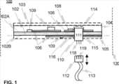
本発明の一実施形態によれば、電子デバイスと共に使用するのに適した統合型の多層構造は、
フィルムの対応する第1面(first surface)と第2面(second surface)とも称される、第1面(first side)と対向する第2面(second side)とを有し、電気的に実質的に絶縁性の材料を含む(第1)基板フィルムと、
任意選択的に接触パッド及び/又は細長い導体トレースを画定する、導電性材料のいくつかの導電性領域を備え、基板フィルムの第1面及び/又は第2面の上に、好ましくはプリンテッド・エレクトロニクス技術によって印刷された回路設計であって、任意選択的に、いくつかの導電性領域のうちの1つ又は複数に対して電気的に接続された、取り付けられた部品及び/又は印刷された部品などの、いくつかの電子部品をさらに備える、回路設計と、
いくつかの導電性接点要素を備え、任意選択的にピン又はボックスヘッダを備えるコネクタであって、このコネクタが、好ましくは基板フィルムを通して、基板フィルムに設けられ、これにより、このコネクタが、基板フィルムの第1面と第2面の両方へと延在し、かついくつかの導電性接触要素が、回路設計の導電性領域のうちの1つ又は複数へと接続し、一方でいくつかの導電性接触要素が、外部接続要素を基板フィルムの第1面又は第2面の上にある、又は基板フィルムに隣接する一体型コネクタと嵌合したことに応答して、外部接続要素に対して電気的に結合されるようにさらに構成されている、コネクタと、
コネクタを少なくとも部分的に覆い、かつ基板フィルムに対する一体型コネクタの固定を増強するように、基板フィルムの第1面及び/又は第2面の上にモールドされた、好ましくは熱可塑性材料からなる、少なくとも1つのプラスチック層と、を含む。
According to one embodiment of the invention, an integrated multilayer structure suitable for use with an electronic device comprises:
having a first side and an opposite second side, also referred to as the corresponding first and second surfaces of the film, and substantially electrically a (first) substrate film comprising a substantially insulating material;
preferably printed on the first side and/or the second side of the substrate film, comprising several conductive areas of conductive material, optionally defining contact pads and/or elongated conductor traces; Circuit design printed by electronic techniques, optionally with attached parts and/or printed electrically connected to one or more of several conductive areas a circuit design that further comprises some electronic components, such as components;
A connector comprising several electrically conductive contact elements and optionally comprising pins or box headers, the connector preferably being provided through the substrate film to the substrate film whereby the connector is connected to the substrate film and some conductive contact elements connect to one or more of the conductive regions of the circuit design, while some conductive The electrical contact element electrically contacts the external connection element in response to mating the external connection element with an integral connector on or adjacent to the first surface or the second surface of the substrate film. a connector further configured to be positively coupled;
of a preferably thermoplastic material molded onto the first and/or second side of the substrate film so as to at least partially cover the connector and enhance the fixation of the integrated connector to the substrate film; and at least one plastic layer.
好ましい実施形態では、上記において言及したように、コネクタの一部分は、例えば、基板の少なくとも1つの穴を介して、基板フィルムを物理的に通して設けられる。これに加えてあるいはこれに代えて、コネクタの少なくとも1つの特徴部は、基板の対向する面の間で、基板の一方の側から縁を超えてもう一方の側へと延在する接続ブリッジ又は同様の構造を画定してもよい。よって、コネクタは、実施形態に応じて、少なくとも機能的に、好ましくは物理的に、基板フィルムを通して設けられてもよい。実際、コネクタを実装するための異なる実施形態について、以下においてより詳細に説明する。 In a preferred embodiment, as mentioned above, a portion of the connector is provided physically through the substrate film, eg, via at least one hole in the substrate. Additionally or alternatively, at least one feature of the connector includes a connecting bridge or a connecting bridge extending from one side of the substrate across the edge to the other side between the opposing surfaces of the substrate. Similar structures may be defined. Thus, connectors may be provided, at least functionally, preferably physically, through the substrate film, depending on the embodiment. Indeed, different embodiments for implementing the connector are described in more detail below.
様々な実施形態では、上述の(熱可塑性)プラスチック材料は、モールドされた材料を受け入れる側の基板の面上に、コネクタを実質的に完全に覆うように構成されてもよい。しかしながら、基板の反対側の面上に位置するコネクタの部分、及び/又は、基板に隣接するコネクタの部分は、例えば、モールドされた材料が少なくとも部分的にないままにされてもよい。 In various embodiments, the (thermoplastic) plastic material described above may be configured to substantially completely cover the connector on the side of the substrate that receives the molded material. However, portions of the connector located on the opposite side of the substrate and/or portions of the connector adjacent to the substrate may, for example, be left at least partially free of molded material.
なお、上記の外部接続要素は、本明細書において提案する多層構造に対してコネクタを介して接続される外部構造、外部デバイス、又は外部システムの実現可能なあらゆる接続特徴部を指す場合がある。そのような接続要素は、すなわち、一般的に接続は、例えば、(剛直な)コネクタ、フレックスケーブル、フレックス回路又はフレックス回路基板、接触ピン(複数可)、接触パッド(複数可)、半田接続、回路基板に対しての半田付け、エポキシ又は接着剤などの導電性接着剤、圧着接続、溶接、等を含むことができる。 It should be noted that the above external connection elements may refer to any possible connection feature of an external structure, external device or system that is connected via a connector to the multi-layer structure proposed herein. Such connection elements, i.e. connections in general, are for example (rigid) connectors, flex cables, flex circuits or flex circuit boards, contact pin(s), contact pad(s), solder connections, Soldering to a circuit board, conductive adhesives such as epoxies or adhesives, crimp connections, welding, and the like can be included.
様々な追加的な実施形態あるいは様々な補足的な実施形態では、回路設計は、いくつかの導電性領域のうちの1つ又は複数に対して少なくとも電気的に接続された、取り付けられた構成部品及び/又は印刷された構成部品などの、いくつかの電子部品をさらに含む。 In various additional embodiments or various supplementary embodiments, the circuit design includes attached components that are at least electrically connected to one or more of several conductive regions. and/or further includes some electronic components such as printed components.
様々な追加的あるいは補足的な実施形態では、回路設計は、任意選択的にブリッジ、回路、及び/又は他のデバイスを含む、ピンなどの複数の接触要素どうしを一緒に接続するように構成されて、それらを介して大電流が流れることを可能とする接続部品をさらに含む。 In various additional or supplemental embodiments, the circuit design is configured to connect together multiple contact elements, such as pins, optionally including bridges, circuits, and/or other devices. , further including connection components that allow high currents to flow through them.
様々な追加的な実施形態あるいは様々な補足的な実施形態では、コネクタは、好ましくは電気絶縁性の(例えば、プラスチック、セラミック、これらの組合せ、又は同様の材料を含む)、ピンなどのいくつかの導電性接触要素を収容する本体部材を含む。本体部材は、基板フィルムの第1面又は第2面に接触するように構成されてもよい。本体部材は、フィルムを通して延びるように構成されてもよい。それでもなお、本体部材は、実質的な弛みを引き起こすことなく、これを通して延びる基板の穴を本質的に収容するような寸法にされてもよい。 In various additional or supplementary embodiments, the connector is preferably electrically insulating (e.g., comprising plastic, ceramic, combinations thereof, or similar materials), some number of pins, etc. a body member housing the conductive contact elements of the. The body member may be configured to contact the first side or the second side of the substrate film. The body member may be configured to extend through the film. Nevertheless, the body member may be sized to essentially accommodate the hole in the substrate extending therethrough without causing substantial slack.
様々な追加的な実施形態あるいは様々な補足的な実施形態では、一体型コネクタ要素は、例えば、典型的にはヒラヒラして、かつ可撓性のプラスチックフィルムとは対照的に、実質的に剛直であり、任意選択的に、いくつかの接触要素のうちの1つ又は複数の接触要素などのいくつかの曲げられた要素が設けられる。曲げられた要素は、基板に対して、及び一般的に多層構造に対して、コネクタの機械的固定を追加するように構成されてもよく、しかも、曲げられた要素は、関連する電気的結合をさらに増強する場合がある。 In various additional embodiments or various supplementary embodiments, the integral connector element is substantially rigid, as opposed to, for example, plastic films that typically flutter and are flexible. and optionally several bent elements such as one or more of several contact elements are provided. The bent elements may be configured to add mechanical fixation of the connector to the substrate, and generally to the multi-layer structure, yet the bent elements provide associated electrical coupling. may further enhance the
様々な追加的あるいは補足的な実施形態では、少なくとも1つのプラスチック層のうちの1つのプラスチック層は、基板フィルムの一方の面(第1面あるいは第2面)の上に位置し、コネクタのうちの、外部接続要素に接触するための部分は、フィルムの反対側の面上に位置している。しかしながら、いくつかの他の実施形態では、基板フィルムの、外部接続要素と嵌合するように構成されたコネクタの部分を含有する側の面上に、代替的な又は追加的なプラスチック層を設けてもよい。 In various additional or supplementary embodiments, one of the at least one plastic layers overlies one side (first side or second side) of the substrate film and is positioned on the connector. , for contacting external connection elements, is located on the opposite side of the film. However, in some other embodiments, an alternative or additional plastic layer is provided on the side of the substrate film containing the portion of the connector configured to mate with the external connection element. may
様々な追加的あるいは補足的な実施形態では、好ましくは弾性的で、任意選択的に返し付き突起及び/又は突出部を画定し又はそれらを備え、好ましくはモールドされた少なくとも1つのプラスチック層によって画定された、いくつかの機械的な係止部材が設けられ、かつ嵌合されると外部接続要素に接触して、一体型コネクタへの外部接続要素の固定を容易にするように構成される。 In various additional or supplementary embodiments, preferably elastic, optionally defining or comprising barbed projections and/or projections, defined by at least one preferably molded plastic layer A number of mechanical locking members are provided and configured to contact the external connection element when mated to facilitate securing the external connection element to the integrated connector.
様々な追加的あるいは補足的な実施形態では、外部コネクタと嵌合した時に、外部コネクタに面し、かつ任意選択的に外部コネクタに接触する部分などのコネクタの一部分は、少なくとも1つのモールドされたプラスチック層によって構築される。 In various additional or supplemental embodiments, a portion of the connector, such as a portion that faces and optionally contacts the external connector when mated with the external connector, includes at least one molded Constructed by plastic layers.
様々な追加的あるいは補足的な実施形態では、コネクタは、少なくとも1つのプラスチック層の中へと入る、返し付き突起などのいくつかの突起を含む。 In various additional or supplementary embodiments, the connector includes a number of projections, such as barbed projections, that penetrate into at least one plastic layer.
様々な追加的あるいは補足的な実施形態では、基板の第1面及び第2面のうちの片面上あるいは有利にも両面上に、回路設計の導電性領域が設けられ、コネクタは、好ましくは、いくつかの接触部材を介して片面上あるいは有利にも両面上において領域に対して直接的に電気接続され、任意選択的に単一の接触部材が、両面上の導電性領域に対して直接的、機械的、かつ電気的に接続される。必要とされる機械的な及び/又は電気的な接続を少なくとも部分的に実装するためには、接着剤の使用、任意選択的に導電性接着剤の使用は、1つの実行可能な選択肢である。 In various additional or supplementary embodiments, conductive areas of the circuit design are provided on one or advantageously both of the first and second sides of the substrate, the connector preferably comprising: Direct electrical connection to the regions on one or advantageously both sides via several contact members, optionally a single contact member directly to the conductive regions on both sides. , are mechanically and electrically connected. To at least partially implement the required mechanical and/or electrical connections, the use of adhesives, optionally conductive adhesives, is one viable option. .
様々な追加的あるいは補足的な実施形態では、基板フィルムは、任意選択的に穴開け、打ち抜き、穿孔、押圧、モールド、又は切断された、少なくとも1つの予め用意された貫通孔を画定し、この貫通孔を通してコネクタがフィルムの第1側及び第2側へと延びる。 In various additional or supplemental embodiments, the substrate film defines at least one pre-prepared through hole, optionally drilled, punched, perforated, pressed, molded, or cut, which Connectors extend through the through holes to the first and second sides of the film.
様々な追加的なあるいは補足的な実施形態では、基板フィルムは、少なくとも1つの貫通孔を画定し、この貫通孔を介して、コネクタの一部分は、第1面もしくは第2面から反対側の第2面もしくは第1面へとそれぞれ延在するように構成されている。貫通孔は、例えば、関連する穿孔操作又は圧着操作によって、コネクタの設置時にコネクタ自身によって構築されていてもよい。 In various additional or supplemental embodiments, the substrate film defines at least one through-hole through which a portion of the connector extends from the first side or the second side to the opposite side. It is configured to extend to two sides or to the first side, respectively. The through-holes may have been constructed by the connector itself during installation of the connector, for example by associated drilling or crimping operations.
様々な追加的なあるいは補足的な実施形態では、コネクタの(任意選択的にコネクタの本体の)基板フィルムに面している部分の表面積は、少なくとも1つの貫通孔の直径より大きな寸法とされ、これにより、コネクタは、少なくとも1つの貫通孔に、完全に適合して通りはしない。 In various additional or supplementary embodiments, the surface area of the portion of the connector (optionally the body of the connector) facing the substrate film is sized larger than the diameter of the at least one through hole, Thereby, the connector does not pass through the at least one through-hole in a perfect fit.
様々な追加的あるいは補足的な実施形態では、接触要素のうちの少なくとも1つは、回路設計の少なくとも1つの導電性領域上へと、任意選択的にバネの力を介して圧縮力を印加するように構成されている。 In various additional or supplemental embodiments, at least one of the contact elements applies a compressive force, optionally via a spring force, onto at least one conductive region of the circuit design. is configured as
様々な追加的あるいは補足的な実施形態では、いくつかの接触要素のうちの少なくとも1つの接触要素は、曲げられており、任意選択的には実質的に角度を形成するようにあるいは具体的にはL字形状を画定するように曲げられており、これにより、基板フィルムの第1面あるいは第2面の上では、接触要素の第1部分が、フィルムの表面に対して実質的に垂直に延在することによって、外部コネクタと接続され、一方で、基板フィルムの反対側の第2面又は第1面の上においては、接触要素の第2部分が、基板フィルムに対して実質的に平行に延在することによって、基板フィルム上における回路設計のいくつかの導電性領域のうちの1つの導電性領域に対して接触する。 In various additional or supplementary embodiments, at least one contact element of the number of contact elements is curved, optionally substantially forming an angle or specifically is bent to define an L-shape such that on the first or second side of the substrate film, the first portion of the contact element is substantially perpendicular to the surface of the film. Extending to connect with an external connector, while on the opposite second or first side of the substrate film the second portion of the contact element is substantially parallel to the substrate film. contacts one of several conductive areas of the circuit design on the substrate film.
様々な追加的あるいは補足的な実施形態では、相手側要素が、すなわち、一般的には係止要素が、任意選択的には係止フレームが設けられる。相手側要素は、任意選択的に、一体型コネクタに対して着脱可能に取り付けられて、基板フィルムへの一体型コネクタの固定を増強してもよく、及び/又は、一体型コネクタに対して外部接続要素を案内してもよい。 In various additional or supplementary embodiments, a mating element is provided, ie generally a locking element and optionally a locking frame. A mating element may optionally be removably attached to the integral connector to enhance the fixation of the integral connector to the substrate film and/or to provide external attachment to the integral connector. A connecting element may be guided.
様々な追加的あるいは補足的な実施形態では、上記の相手側要素、すなわち、係止要素は、導電性材料からなる、板バネなどの少なくとも1つのバネ状の要素を含み、この少なくとも1つのバネ状の要素が、一体型コネクタの少なくとも1つの接触要素と基板フィルムの少なくとも1つの導電性領域との両方に接触して、それら2つの間の電気的結合を増強する。 In various additional or complementary embodiments, said mating element, i.e. the locking element, comprises at least one spring-like element, such as a leaf spring, made of an electrically conductive material, said at least one spring A shaped element contacts both the at least one contact element of the integrated connector and the at least one conductive region of the substrate film to enhance electrical coupling between the two.
様々な追加的あるいは補足的な実施形態では、相手側要素/係止要素は、基板フィルムに面する表面積を、基板フィルムのこれを通して一体型コネクタが通る1つ又は複数の貫通孔によって画定される表面積よりも大きいように画定する。 In various additional or supplementary embodiments, the mating element/locking element has a surface area facing the substrate film defined by one or more through-holes in the substrate film through which the integral connector passes. Defined to be larger than the surface area.
様々な追加的あるいは補足的な実施形態では、基板フィルムの領域上に、任意選択的にガスケットとされる、機械的な封止部材が設けられ、この機械的な封止部材は、外部コネクタを受け入れるように構成され、好ましくは、基板フィルムと、当該基板フィルム上に配置された外部コネクタとの間に、気密封止を提供する。 In various additional or supplementary embodiments, a mechanical sealing member, optionally a gasket, is provided over the area of the substrate film, the mechanical sealing member connecting the external connector. It is adapted to receive and preferably provides a hermetic seal between the substrate film and an external connector disposed on the substrate film.
様々な追加的なあるいは補足的な実施形態では、基板フィルムは、本体部材の一部分などのコネクタの一部分及び/又はその接触要素を収容する凹部を画定し、かつ好ましくはその凹部の底部にこれを介してコネクタが基板フィルムを貫通する貫通孔を有する。 In various additional or supplementary embodiments, the substrate film defines a recess for housing a portion of the connector, such as a portion of the body member, and/or its contact elements, and preferably mounts it at the bottom of the recess. The connector has a through hole through the substrate film.
様々な追加的あるいは補足的な実施形態では、コネクタは、任意選択的にその本体部材内に、角度付きの、傾斜した、又は湾曲した表面を備え、コネクタは、角度付き、傾斜した、又は湾曲した表面が、基板の隣接する表面に、例えば基板の輪郭に実質的に追従するように、基板に対して構成される。 In various additional or supplemental embodiments, the connector optionally includes an angled, slanted or curved surface within its body member, wherein the connector is angled, slanted or curved. The contoured surface is configured with respect to the substrate to substantially follow the adjacent surface of the substrate, eg, the contour of the substrate.
様々な追加的あるいは補足的な実施形態では、コネクタは、基板フィルムを、穿孔、打ち抜き、又は他の方法で貫通するように構成されると共に、好ましくは、基板に対して、特にその上に提供された回路設計の1つ又は複数の導電性領域に対して、圧着接続を画定する。圧着接続は、例えば、バネ接続を含んでもよい。 In various additional or supplementary embodiments, the connector is configured to perforate, punch, or otherwise penetrate the substrate film and is preferably provided to, and particularly on, the substrate. A crimp connection is defined to one or more conductive regions of the designed circuit design. A crimp connection may include, for example, a spring connection.
様々な追加的あるいは補足的な実施形態では、コネクタは、基板フィルムの対向する側に設けられ、かつ基板フィルムを通して少なくとも機能的に一緒に接続された、すなわち、例えばフィルムの穴を介してフィルムを実際に物理的に貫通して一緒に接続された、及び/又は他のところでより詳細に説明するように、基板フィルムの縁を取り囲んで一緒に接続された、少なくとも2つの部分あるいは少なくとも2つの(サブ)コネクタを含む。 In various additional or supplementary embodiments, the connectors are provided on opposite sides of the substrate film and are at least functionally connected together through the substrate film, i.e., the films through holes in the film. At least two portions or at least two (at least two ( sub) connector.
様々な追加的あるいは補足的な実施形態では、そのような2つの対向する部分のうちの少なくとも一方は、いくつかの突起を含み、前記いくつかの突起が、基板フィルムを通して設けられ、任意選択的には、基板フィルム上の回路設計の導電性領域をさらに通して設けられるか、もしくは導電性領域に隣接して設けられ、かつもう一方の部分と接続する。 In various additional or supplementary embodiments, at least one of such two opposing portions comprises a number of protrusions, said number of protrusions being provided through the substrate film, optionally is provided through or adjacent to the conductive area of the circuit design on the substrate film and connects to the other portion.
様々な追加的あるいは補足的な実施形態では、少なくとも2つの部分は、これらの間に構築された、任意選択的に少なくとも部分的にそれらの部分のいずれかの材料からなる、いくつかの好ましくは溶接された中間特徴部によって接続されている。 In various additional or supplementary embodiments, the at least two portions are constructed therebetween, optionally at least partially, of any material of those portions, some preferably Connected by welded intermediate features.
様々な追加的あるいは補足的な実施形態では、コネクタは、基板の縁を超えて延在し、かつ少なくとも2つの対向する部分を接続し、任意選択的に少なくとも2つの対向する部分を有するモノリシック構造である、少なくとも1つのブリッジ部分を備える。 In various additional or supplemental embodiments, the connector extends beyond the edge of the substrate and connects at least two opposing portions, optionally a monolithic structure having at least two opposing portions. and at least one bridging portion.
様々な追加的あるいは補足的な実施形態では、コネクタは、外部接続要素との結合のために、基板から側方へと延在する突出部分を画定する。 In various additional or supplemental embodiments, the connector defines a projecting portion extending laterally from the substrate for coupling with an external connection element.
様々な追加的あるいは補足的な実施形態では、基板フィルムは本質的に平面状であるか、あるいは少なくとも局所的に本質的に3次元形状を示し、任意選択的に、湾曲した、角度付きの、傾斜した、又はドーム形状を示す。 In various additional or complementary embodiments, the substrate film is essentially planar or exhibits at least locally an essentially three-dimensional shape, optionally curved, angled, Shows a slanted or domed shape.
様々な追加的あるいは補足的な実施形態では、回路設計は、好ましくはモールドされた少なくとも1つのプラスチック層内に少なくとも部分的に埋め込まれた、電子部品又は電子デバイス又は光電子部品又は光電子デバイスなどのいくつかの構成部品をさらに備えるか、あるいは、これらに対して少なくとも電気的に接続されている。 In various additional or supplementary embodiments, the circuit design preferably comprises any number of electronic components or devices or optoelectronic components or optoelectronic devices at least partially embedded within at least one molded plastic layer. further comprising, or at least electrically connected to, any of the components.
様々な追加的あるいは補足的な実施形態では、コネクタは、いくつかの電子部品及び/又は接続部品を、任意選択的に少なくとも1つの集積回路をさらに備える。 In various additional or supplementary embodiments, the connector further comprises several electronic components and/or connecting components, optionally at least one integrated circuit.
様々な追加的あるいは補足的な実施形態では、一体型コネクタ、任意選択的には一体型コネクタの本体部材は、モールドされたプラスチックによって少なくとも部分的に充填された空洞を含む。これは、一般に、基板及び多層構造に対してのコネクタ要素の固定を増強する場合がある。 In various additional or supplemental embodiments, the unitary connector, optionally the body member of the unitary connector, includes a cavity that is at least partially filled with molded plastic. This may generally enhance the fixation of the connector element to the substrate and multilayer structure.
様々な追加的あるいは補足的な実施形態では、基板フィルム(複数可)は、例えば熱可塑性ポリマー等のプラスチックなどの、及び/又は、例えば木材、革、布地、又はこれらの材料のいずれかと相互の組合せ又はこれら材料のいずれかとプラスチックもしくはポリマーもしくは金属との組合せ等の有機材料又は生体材料などの、1つ又は複数の材料を含むことができる、あるいはそのような材料(複数可)からなってもよい。基板フィルムは、熱可塑性材料を含んでもよく、あるいは熱可塑性材料からなってもよい。フィルムは、本質的に、可撓性であってもよく、あるいは屈曲可能であってもよい。いくつかの実施形態では、フィルムは、代替的に、実質的に剛直であってもよい。フィルムの厚さは、実施形態に依存して変更されてもよく、その厚さは、わずかに数十ミリメートル又は数百ミリメートルであってもよく、あるいはかなり厚いものとすることができ、例えば、1ミリメートル又は数ミリメートルという程度であってもよい。 In various additional or supplementary embodiments, the substrate film(s) is made of plastic, such as a thermoplastic polymer, and/or is compatible with, for example, wood, leather, fabric, or any of these materials. It may comprise or consist of one or more materials, such as organic materials or biomaterials, such as combinations or combinations of any of these materials with plastics or polymers or metals. good. The substrate film may comprise or consist of a thermoplastic material. The film may be flexible or bendable in nature. In some embodiments, the film may alternatively be substantially rigid. The thickness of the film may vary depending on the embodiment, and may be as little as tens or hundreds of millimeters, or may be significantly thicker, e.g. It may be of the order of a millimeter or a few millimeters.
基板フィルムは、例えば、ポリマー、熱可塑性材料、電気絶縁材料、PMMA(ポリメチルメタクリレート)、ポリカーボネート(PC)、コポリエステル、コポリエステル樹脂、ポリイミド、メタクリル酸メチルとスチレンのコポリマー(MS樹脂)、ガラス、ポリエチレンテレフタレート(PET)、炭素繊維、有機材料、生体材料、革、木材、布、布地、金属、有機天然材料、無垢材、ベニヤ、合板、木の皮、樹皮、白樺の樹皮、コルク、天然皮革、天然の布素材又は布地素材、天然素材、綿、羊毛、麻、絹、及び、これらの任意の組合せ、からなる群から選択される少なくとも1つの材料を含んでもよい。 Substrate films are, for example, polymers, thermoplastic materials, electrically insulating materials, PMMA (polymethyl methacrylate), polycarbonate (PC), copolyesters, copolyester resins, polyimides, copolymers of methyl methacrylate and styrene (MS resins), glass , polyethylene terephthalate (PET), carbon fiber, organic material, biomaterial, leather, wood, cloth, fabric, metal, organic natural material, solid wood, veneer, plywood, tree bark, bark, birch bark, cork, natural It may comprise at least one material selected from the group consisting of leather, natural cloth or textile materials, natural materials, cotton, wool, linen, silk, and any combination thereof.
さらなる、補足的な又は代替可能な実施形態では、含まれるフィルムの1つ又は複数は、例えば可視スペクトル内の波長などの所定の波長に関して、少なくとも部分的に光学的に実質的に不透明なもの、あるいは少なくとも半透明なものであってもよい。フィルムには、フィルム上に又はフィルム内に、グラフィックパターン及び/又は色などの、視覚的区別が可能な特徴部、装飾的/審美的な特徴部、及び/又は情報を与える特徴部がその上に提供されてもよい。特徴部は、フィルムの電子機器が設けられているのと同じ側に提供されてもよく、これにより、特徴部を、関連するオーバーモールド手順を通してプラスチック材料(複数可)によって少なくとも部分的に封止されてもよい。したがって、IML(インモールドラベリング)/IMD(インモールドデコレーション)技法が適用可能である。フィルム(複数可)は、フィルム上の電子機器から放出される可視光などの放射に対して、少なくとも部分的に、すなわち少なくとも場所によって、光学的に実質的に透明なものとしてもよい。透過率は、例えば、およそ、80%、85%、90%、95%、あるいはそれ以上であってもよい。 In further, supplemental or alternative embodiments, one or more of the included films are at least partially optically substantially opaque for predetermined wavelengths, such as wavelengths within the visible spectrum; Alternatively, it may be at least translucent. The film may additionally have visually distinguishable, decorative/aesthetic, and/or informational features, such as graphic patterns and/or colors, on or in the film. may be provided to The features may be provided on the same side of the film as the electronics are provided, whereby the features are at least partially encapsulated by the plastic material(s) through a related overmolding procedure. may be Therefore, IML (in-mold labeling)/IMD (in-mold decoration) techniques are applicable. The film(s) may be substantially optically transparent, at least partially, ie, at least locally, to radiation, such as visible light, emitted from electronics on the film. The transmittance may be, for example, approximately 80%, 85%, 90%, 95%, or more.
基板フィルム(複数可)の上へとモールドされたプラスチック層(複数可)は、ポリマー、有機物、生体材料、複合体、ならびに、これらの任意の組合せ、などの材料を含むことができる。モールドされた材料は、熱可塑性材(複数可)、及び/又は熱硬化性材料(複数可)を含んでもよい。モールドされた層の(複数可)厚さは、実施形態に依存して変更され得る。そのような厚さは、例えば、1ミリメートル、数ミリメートル、又は、数十ミリメートル、という大きさの程度であってもよい。モールドされた材料は、例えば、電気絶縁性であってもよい。 The plastic layer(s) molded onto the substrate film(s) can include materials such as polymers, organics, biomaterials, composites, and any combination thereof. The molded material may include thermoplastic material(s) and/or thermoset material(s). The thickness(es) of the molded layer(s) may vary depending on the embodiment. Such thickness may be, for example, on the order of magnitude of one millimeter, several millimeters, or tens of millimeters. The molded material may be electrically insulating, for example.
より詳細には、少なくとも1つのモールドされたプラスチック層は、エラストマー樹脂、熱硬化性材料、熱可塑性材料、PC、PMMA、ABS、PET、コポリエステル、コポリエステル樹脂、ナイロン(PA、ポリアミド)、PP(ポリプロピレン)、TPU(熱可塑性ポリウレタン)、ポリスチレン(GPPS)、TPSiV(熱可塑性シリコーン加硫ゴム)、及び、MS樹脂、からなる群から選択される少なくとも1つの材料を含んでもよい。 More particularly, the at least one molded plastic layer is made of elastomer resin, thermoset material, thermoplastic material, PC, PMMA, ABS, PET, copolyester, copolyester resin, nylon (PA, polyamide), PP (polypropylene), TPU (thermoplastic polyurethane), polystyrene (GPPS), TPSiV (thermoplastic silicone vulcanizate), and at least one material selected from the group consisting of MS resin.
いくつかの実施形態では、モールドされた層を確立するために使用される(熱可塑性)プラスチック材料は、光学的に実質的に、不透明な材料、透明な材料、又は半透明な材料を含み、例えば可視光を、ごくわずかな損失でもってモールドされた層を通過させることができる。所望の波長における充分な透過率は、例えば、およそ、80%、85%、90%、95%、あるいはそれ以上であってもよい。可能なさらなるモールドされた(熱可塑性)プラスチック材料は、実質的に不透明なもの又は半透明なものであってもよい。いくつかの実施形態では、さらなる材料は、透明であってもよい。 In some embodiments, the (thermoplastic) plastic material used to establish the molded layer comprises an optically substantially opaque, transparent, or translucent material, For example, visible light can pass through the molded layer with negligible loss. Sufficient transmission at desired wavelengths may be, for example, approximately 80%, 85%, 90%, 95%, or more. Possible further molded (thermoplastic) plastic materials may be substantially opaque or translucent. In some embodiments, the additional material may be transparent.
様々な追加的あるいは補足的な実施形態では、導電性領域は、導電性インク、導電性ナノ粒子インク、銅、鋼、鉄、スズ、アルミニウム、銀、金、白金、導電性接着剤、炭素繊維、合金、銀合金、亜鉛、真鍮、チタン、半田、及び、これらの任意の成分、からなる群から選択される少なくとも1つの材料を含む。使用される導電性材料は、例えば可視光などの所望の波長において、可視光などの放射を、例えば、それらから反射させる、それらに吸収させる、又は透過させるために、遮断もしくは遮蔽するように、光学的に不透明なもの、半透明なもの、及び/又は透明なものであってもよい。 In various additional or supplementary embodiments, the conductive region may be conductive ink, conductive nanoparticle ink, copper, steel, iron, tin, aluminum, silver, gold, platinum, conductive adhesives, carbon fiber, , alloys, silver alloys, zinc, brass, titanium, solder, and any component thereof. The conductive material used is such that it blocks or shields radiation, such as visible light, at a desired wavelength, such as visible light, for example to reflect from, absorb into, or transmit. It may be optically opaque, translucent and/or transparent.
様々な追加的あるいは補足的な実施形態では、コネクタの接触要素は、銅、銀、金、白金、導電性接着剤、炭素繊維、亜鉛、真鍮、合金、及び、銀合金、からなる群から選択される少なくとも1つの材料を含む。この場合にも、材料は、任意選択的に、所望の導電性に加えて、透明性、半透明性、又は不透明性などの、例えば、所望の光学特性を示すように、選択されてもよい。 In various additional or supplemental embodiments, the connector contact elements are selected from the group consisting of copper, silver, gold, platinum, conductive adhesives, carbon fiber, zinc, brass, alloys, and silver alloys. at least one material that is Again, the material may optionally be selected to exhibit desired optical properties, such as transparency, translucency, or opacity, in addition to the desired electrical conductivity. .
様々な追加的あるいは補足的な実施形態では、コネクタは、ピンヘッダ、圧着コネクタ、バネ状の接触部材、バネ付き接触部材、バネ付きの接触ピン又はスリップ、接触パッド、接触領域、接触ピン、好ましくは導電性材料からなる壁及び/又は底部を有する穴、ソケット、メス型のソケット、オス型のプラグ又はソケット、ハイブリッドソケット、ピンソケット、及びバネピンソケット、からなる群から選択される少なくとも1つの特徴部を含む。 In various additional or supplementary embodiments, the connector comprises a pin header, a crimp connector, a spring-like contact member, a spring-loaded contact member, a spring-loaded contact pin or slip, a contact pad, a contact area, a contact pin, preferably a at least one feature selected from the group consisting of holes having walls and/or bottoms made of electrically conductive material, sockets, female sockets, male plugs or sockets, hybrid sockets, pin sockets, and spring pin sockets. including part.
それでもなお、多層構造の実施形態と、構造のコネクタ要素との嵌合に関して互換的な外部要素の実施形態と、を含むシステムが提供される場合がある。 Nonetheless, systems may be provided that include embodiments of multi-layer structures and embodiments of external elements that are interchangeable with respect to mating with the connector elements of the structure.
本発明の1つの他の実施形態によれば、多層構造を製造するための方法は、
電子機器を収容するための、可撓性のプラスチックフィルムなどの(第1)基板フィルムを入手することであって、互いに対向する第1面(side)及び第2面(side)とそれぞれの表面(surface)とを有する基板フィルムを、入手することと、
好ましくは少なくとも部分的にプリンテッド・エレクトロニクス技術によって、基板フィルムの第1面及び/又は第2面の上に、導電性材料のいくつかの導電性領域を備える回路設計を設けることと、
いくつかの導電性接触要素を備える電気コネクタを、任意選択的に少なくとも機能的にかつ好ましくは物理的に基板フィルムを通して、基板フィルムに配設することであって、これにより電気コネクタが基板フィルムの第1面と第2面との両方へと延在し、かついくつかの導電性接触要素が、回路設計の導電性領域に対して接続され、一方で、外部接続要素を、基板フィルムの第1面もしくは第2面の上にある、又はこれに隣接するコネクタと嵌合することに応答して、外部接続要素へと電気的に結合するようにさらに構成されることと、
任意選択的に射出成形を利用して、基板フィルムの第1面及び/又は第2面の上とコネクタ要素上とに、電気コネクタを材料内に少なくとも部分的に埋め込むように、任意選択的には、外部接続要素が嵌合した時に外部接続要素から離れる側に面した基板の面上にあるコネクタの部分を完全に埋め込むように、熱可塑性材料をモールドすることであって、これによって、コネクタの基板フィルムへの固定を増強することと、を含む。
According to one other embodiment of the invention, a method for manufacturing a multilayer structure comprises:
Obtaining a (first) substrate film, such as a flexible plastic film, for housing electronic devices, having first and second sides facing each other and respective surfaces obtaining a substrate film having a surface;
providing a circuit design comprising several conductive areas of conductive material on the first and/or second side of the substrate film, preferably at least in part by printed electronics techniques;
Disposing an electrical connector comprising a number of electrically conductive contact elements to the substrate film, optionally at least functionally and preferably physically through the substrate film, whereby the electrical connector is disposed on the substrate film. A number of conductive contact elements extending to both the first side and the second side and connected to conductive areas of the circuit design, while external connection elements are connected to the second side of the substrate film. further configured to electrically couple to an external connection element in response to mating with a connector on or adjacent to one or the second surface;
optionally using injection molding to at least partially embed the electrical connector into the material on the first and/or second side of the substrate film and on the connector element; is the molding of a thermoplastic material so as to completely embed the portion of the connector on the side of the substrate facing away from the external connection element when the external connection element is mated, whereby the connector and enhancing the anchoring of the to the substrate film.
この方法は、例えば、上記の方法項目に関連してあるいはその後に、多層構造に対して、追加的な材料(複数可)あるいは追加的な層(複数可)(例えば、フィルム(複数可)、及び/又はモールドされた層(複数可))、及び/又は要素(複数可)を設けることをさらに含んでもよい。1つ又は複数の、追加的な(基板)フィルム又は材料層が、例えば、接着剤、熱及び/又は圧力を使用する既存の層の上への積層を通して構造に対して予め用意された要素として設けられてもよく、あるいは、例えば、モールド、印刷、又は堆積プロセスによってそれらを原材料から構造へと直接的に構築してもよい。 The method may include, for example, in conjunction with or after the method section above, adding additional material(s) or additional layer(s) (e.g., film(s), and/or molded layer(s), and/or element(s). One or more additional (substrate) films or material layers as pre-prepared elements to the structure through lamination onto existing layers using, for example, adhesives, heat and/or pressure or they may be built directly into the structure from raw materials, for example by molding, printing, or deposition processes.
これにより、例えば、第2(基板)フィルムは、任意選択的にモールドされたプラスチックとは反対側に設けられてもよい。第2フィルムは、第1基板フィルムと一緒に金型内に配置されてもよく、これにより、それらの間にプラスチック材料を射出することによって積層構造が得られ、あるいは第2フィルムは、モールドされたプラスチック層上に直接的に製造されない場合に、適切な積層技法を使用して、その後で設けられてもよい。第2フィルムには、そのいずれかの側の面上に(例えば、モールドされたプラスチック層に面して)、グラフィックス、他の光学的特徴部、及び/又は電子機器などの特徴部が設けられてもよい。なお、第2フィルムは、保護という目的、及び/又は、所望の光透過率、外観(例えば、色)、又は触感などの他の技術的特徴点を有する場合がある。第2フィルムは、任意選択的に、一体型コネクタによって、及び/又は導電性材料によって充填された又は導体要素を用いて設けられた1つ又は複数のビアなどの他の接続特徴部によって、第1フィルムに電気的に接続されるなど、動作可能に接続されてもよい。 Thus, for example, a second (substrate) film may optionally be provided on the side opposite the molded plastic. The second film may be placed in a mold together with the first substrate film, resulting in a laminated structure by injecting a plastic material between them, or the second film may be molded. If not manufactured directly onto the plastic layer, it may be subsequently applied using a suitable lamination technique. The second film is provided with features such as graphics, other optical features, and/or electronics on either side thereof (e.g., facing the molded plastic layer). may be It should be noted that the second film may have a protective purpose and/or other technical features such as desired light transmission, appearance (eg, color), or feel. The second film is optionally provided by an integral connector and/or by other connection features such as one or more vias filled with a conductive material or provided with conductive elements. 1 film may be operably connected, such as electrically connected.
様々な実施形態では、材料層及び関連する特徴部を生成するための実現可能なモールド方法は、例えば、熱可塑性材料に関連した射出成形、及び特に熱硬化性材料に関連した反応性射出成形などの反応性成形を含む。いくつかのプラスチック材料の場合には、それらは2ショットモールド法、あるいは一般的にはマルチショットモールド法を使用して、モールドしてもよい。複数のモールドユニットを備えたモールド機械を利用してもよい。これに代えて、いくつかの材料を順次的に提供するために、複数の機械、あるいは単一の再構成可能な機械を使用することができる。 In various embodiments, feasible molding methods for producing material layers and associated features include, for example, injection molding associated with thermoplastic materials, and reactive injection molding particularly associated with thermoset materials. including reactive molding of In the case of some plastic materials they may be molded using a two-shot molding process, or more commonly a multi-shot molding process. A molding machine with multiple molding units may be utilized. Alternatively, multiple machines or a single reconfigurable machine can be used to sequentially provide several materials.
適用可能なモールドプロセスパラメータに関しては、例えば、上記の射出成形及び反応性成形は、使用する材料、必要な材料特性、成形設備等に依存して、一般的には信頼できる選択肢である。下にある電子機器などの特徴部に対する応力を最小とするために、低圧(例えば、約10bar未満)モールドを、第1基板の第2面へのオーバーモールド、ならびに、その上の回路へのオーバーモールドなどの、選択されたモールド操作において、使用してもよい。異なるモールド技法を適用することにより、例えば強度などの所望の機械的特性という点において、構造に対して様々な材料特性をもたらすことができる。 In terms of applicable molding process parameters, for example, injection molding and reactive molding as described above are generally reliable choices depending on the materials used, material properties required, molding equipment, and the like. A low pressure (e.g., less than about 10 bar) mold is overmolded onto the second side of the first substrate as well as the circuitry thereon to minimize stress on underlying features such as electronics. It may be used in selected molding operations, such as molding. The application of different molding techniques can provide different material properties to the structure, for example in terms of desired mechanical properties such as strength.
様々な実施形態では、1つ又は複数の基板フィルムを、好ましくは基板フィルム上に導体、及び電子部品などの任意選択的なさらなる電子機器を設けた後に、しかしながらプラスチック層のモールドの前に、多くの場合、本質的に3次元的な所望の目標形状を少なくとも局所的に呈するようにして、成形してもよく、任意選択的に熱成形又は冷間成形してもよい。フィルムに、例えば、コネクタなどの特徴部の少なくとも一部分を収容するために使用し得る凹部を画定するために、成形を利用してもよい。成形前及び/又はモールド前にフィルム上に既に存在している電子機器などの要素に関する、使用材料、寸法、配置、及び、他の構成は、破損を起こすことなく成形/モールドによってそれらに対して印加される力に耐え得るように選択されるものとする。 In various embodiments, one or more substrate films, preferably after providing conductors and optionally further electronics, such as electronic components, on the substrate film, but prior to molding of the plastic layer, often may be shaped, optionally thermoformed or cold formed, to assume a desired target shape, which is essentially three-dimensional, at least locally. Molding may be utilized to define recesses in the film that may be used to accommodate at least a portion of features such as connectors, for example. The materials used, dimensions, placement, and other configurations of elements such as electronics that are already present on the film prior to forming and/or molding can be applied to them by forming/moulding without causing damage. It shall be selected to withstand the applied force.
様々な実施形態では、基板フィルムには、貫通孔などの少なくとも1つの穴が設けられることとなる。穴は、モールド(あるいは一般的には、穴が設けられたものとして基板フィルムを直接的に確立する)、穴開け、カービング、ソーイング、エッチング、穿孔(例えば、圧着に関連して)、切断(例えば、レーザあるいは機械的ブレードを用いて)、あるいは、当業者であれば理解されるような任意の他の実行可能な方法を使用して、設けられてもよい。 In various embodiments, the substrate film will be provided with at least one hole, such as a through hole. Holes can be formed by molding (or generally directly establishing the substrate film as being perforated), drilling, carving, sawing, etching, perforating (e.g. in connection with crimping), cutting ( for example, using a laser or mechanical blade), or using any other practicable method as would be understood by those skilled in the art.
なお、少なくとも1つの穴は、所望の形状を有してもよく、すなわち実質的に円形の又は角度付きの形状、例えば、矩形形状を有してもよい。好ましくは、穴は、選択された方式でかつ所望の程度にまで、コネクタ要素の形状/寸法に適合するように、形状及び寸法が整えられる。例えば、穴は、コネクタ要素のいくつかの接触要素が貫通することを可能としてもよく、一方で、コネクタ要素の本体が穴を完全に覆って、これにより、例えば穴を封止するほど充分に小さなままとしてもよい。 It should be noted that the at least one hole may have any desired shape, ie a substantially circular or angled shape, for example a rectangular shape. Preferably, the holes are shaped and sized to match the shape/size of the connector element in a selected manner and to the extent desired. For example, the holes may allow some contact elements of the connector element to pass through, while the body of the connector element is sufficient to completely cover the holes, thereby sealing the holes, for example. May be kept small.
いくつかの実施形態では、少なくとも1つの穴のうちの少なくとも1つは、例えば、薄肉化により基板内の止まり穴として形成されてもよい。その場合には、基板に対してコネクタ要素を設けると、ピンなどのコネクタの突起タイプの接触要素は、止まり穴の底部を穿孔、あるいは打ち抜いて、当該フィルムの反対側へと進入するように構成されてもよい。しかしながら、いくつかの補足的な又は代替的な実施形態では、コネクタ要素の、ピン(複数可)など接触要素(複数可)は、止まり穴(複数可)あるいは他の穿孔用に事前に特別に処理された領域(複数可)が設けられていない位置(複数可)で、基板を穿孔するか、あるいは打ち抜くように構成されてもよい。この構成は、必要とされる製造工程又は操作の数を低減するという観点から、便利なものである。したがって、フィルムを通して設けられる要素(複数可)は、それ自体を利用して、設置時に、必要な穴をフィルムに形成することができる。 In some embodiments, at least one of the at least one hole may be formed as a blind hole in the substrate, for example by thinning. In that case, when the connector element is provided to the substrate, the protrusion-type contact elements of the connector, such as pins, are configured to perforate or punch through the bottom of the blind hole and enter the opposite side of the film. may be However, in some supplementary or alternative embodiments, the contact element(s), such as the pin(s), of the connector element are specifically pre-drilled for blind hole(s) or other drilling. It may be configured to perforate or punch the substrate at location(s) not provided with treated region(s). This configuration is convenient from the standpoint of reducing the number of manufacturing steps or operations required. Thus, the element(s) provided through the film can utilize themselves to form the required holes in the film during installation.
様々な実施形態では、基板フィルムを通してコネクタの一部分を提供することに加えて、いくつかの他の穴又はビアを、フィルム(複数可)内に、及び/又は、多層構造のモールドされた層(複数可)などの他の層(複数可)内に構築することができる。これにより、例えば、実際には、関係するフィルム/層の両面上の電子機器どうしを一緒に接続することに関連して、例えば、フィルムの互いに対向する第1面及び第2面を、電気的に及び/又は光学的に一緒に接続する。一般に、そのようなビア、すなわち、基本的には貫通孔は、モールド(あるいは一般的には、穴を有する基板フィルムを直接的に画定する)、穴開け、化学的(例えば、エッチングによって)、カービング、ソーイング、エッチング、例えばレーザあるいは機械的ブレードを使用した切断、または、当業者であれば理解されるような任意の他の実行可能な方法を使用して、対応して設けられる。ビアは、所望の断面形状を有することができる、すなわち、実質的に円形の又は角を有する形状を有してもよく、例えば、矩形形状又は細長い(スリット)形状を有してもよい。 In various embodiments, in addition to providing a portion of the connector through the substrate film, several other holes or vias are provided in the film(s) and/or molded layers ( It can be built within other layer(s) such as layer(s). Thus, for example, in practice, in connection with connecting together the electronics on both sides of the films/layers involved, for example, the first and second opposite sides of the film can be electrically and/or optically connected together. Generally, such vias, or basically through holes, are molded (or generally directly defining a substrate film with holes), drilled, chemically (e.g., by etching), Correspondingly provided using carving, sawing, etching, cutting, for example using a laser or a mechanical blade, or any other feasible method as would be understood by those skilled in the art. The vias can have any desired cross-sectional shape, ie they may have a substantially circular or angled shape, for example they may have a rectangular shape or an elongated (slit) shape.
上述したビアは、モールド、取り付け、又は印刷などの選択された充填方法を使用して、導電性材料及び/又は光透過性材料などの選択された材料(複数可)を用いて設けてもよい。そのような材料は、接着剤、エポキシ、金属、導電性インク、気体物質又は液体物質などの流体材料等を含んでもよい。そのような材料は、例えば曲げ歪みに耐え得るように形成可能であってもよい。いくつかの実施形態では、大気センサなどの内部センサがビアを介して環境に動作可能に結合できるようにするために、ビア(複数可)は、開放したまま(充填されていない)であってもよい。 The vias described above may be provided with selected material(s) such as electrically conductive and/or light transmissive materials using selected filling methods such as molding, attaching or printing. . Such materials may include adhesives, epoxies, metals, conductive inks, fluid materials such as gaseous or liquid substances, and the like. Such materials may be formable to withstand bending strains, for example. In some embodiments, the via(s) are left open (unfilled) to allow an internal sensor, such as an air sensor, to be operatively coupled to the environment through the via. good too.
様々な実施形態では、電子部品又は他の要素などの1つ又は複数の特徴部を、例えば、(追加的に)プリンテッド・エレクトロニクス技術、減法的製造技法、及び/又は、例えば、SMD/SMT(表面実装デバイス/表面実装技術)に関連した実装によって、多層構造のフィルム又はモールドされた層などの目標基板に設けてもよい。1つ又は複数の特徴部は、モールドされたプラスチックによって少なくとも部分的に覆われた基板領域上に設けられてもよく、その結果、その特徴部自体もまた、モールドされたプラスチックによって少なくとも部分的に覆われる。 In various embodiments, one or more features, such as electronic components or other elements, may be fabricated using, for example, (additionally) printed electronics techniques, subtractive manufacturing techniques, and/or, for example, SMD/SMT. It may be applied to a target substrate such as a multi-layered film or molded layer by mounting related to (Surface Mount Device/Surface Mount Technology). One or more features may be provided on a substrate region that is at least partially covered by molded plastic, such that the feature itself is also at least partially covered by molded plastic. covered.
様々な方法項目の相互的な実行順序は、特定の実施形態ごとに異なり得るものであって、事例ごとに決定されてもよい。例えば、第1基板フィルムの第2面は、第1面の前、第1面の後、又は実質的に同時に、オーバーモールドされてもよく、例えば、モールドされた材料は、例えば既存の貫通孔を介して、又は圧力によって誘起された貫通孔を介して、モールドされた材料がフィルムの最初の側から反対の側へと伝播するように、射出されてもよい。 The order of execution of various method items relative to each other may vary for particular implementations and may be determined on a case-by-case basis. For example, the second side of the first substrate film may be overmolded before the first side, after the first side, or substantially simultaneously, e.g. or through pressure-induced through-holes so that the molded material propagates from the first side of the film to the opposite side.
多層構造の様々な実施形態に関して上記で提示した考慮事項は、当業者であれば理解されるように、必要な変更を加えて、関連する製造方法の実施形態に対して、柔軟に適用することができ、逆もまた同様である。なお、様々な実施形態及び関連する特徴部は、本明細書において一般的に開示される特徴部どうしの好ましい組合せを想起し得るよう、当業者であれば柔軟に組み合わせることができる。 The considerations presented above with respect to the various embodiments of the multilayer structure can be flexibly applied mutatis mutandis to the relevant manufacturing method embodiments, as will be appreciated by those skilled in the art. and vice versa. It should be noted that the various embodiments and associated features can be flexibly combined by those skilled in the art to conceive preferred combinations of features generally disclosed herein.
本発明の有用性は、実施形態に応じた複数の事柄から生じる。 The usefulness of the present invention arises from several things depending on the embodiment.
外部デバイス、システム、又は構造に対して、例えば電力及び/又は通信などの電気的な接続を提供するための、電気コネクタ構造又はコネクタ要素、あるいは単にコネクタは、便利で信頼性高くかつ優れた視覚的品質を有しており、例えば一般的にIMSE原則に従って製造された、機能的な回路設計及び様々な電子機器を含む多層構造内に、統合されて固定され、埋め込まれてもよい。 Electrical connector structures or connector elements, or simply connectors, for providing electrical connections, e.g., power and/or communications, to external devices, systems, or structures are convenient, reliable, and visually appealing. may be integrated, fixed and embedded within multi-layer structures containing functional circuit designs and various electronic devices, for example generally manufactured according to IMSE principles, having a mechanical quality.
いくつかの実施形態では、導電性領域(複数可)は、例えばプリンテッド・エレクトロニクス技術によって、基板の片面又は両面/表面の上のいずれかに、基板上に最初に設けられてもよい。続いて、任意選択的に、フィルム内の予め用意された、いくつかの穴を部分的に通してコネクタを設けることによって、あるいは、例えば、コネクタを圧着することにより及び/又は例えばコネクタ(の接触要素)によりフィルムを穿孔することにより、その場で穴を形成することによって、基板の両側へと延びるようにコネクタを基板に対して提供してもよい。これに加えてあるいはこれに代えて、基板の縁を取り囲む接続を利用することにより、基板の両面上のコネクタ部分どうしを相互に接続することができる、すなわち一般的には、それらコネクタ部分どうしの相互接続を提供することができる。その場合でも、コネクタは、少なくとも機能的に基板フィルムを貫通して設けられていると言うことができる。 In some embodiments, the conductive region(s) may be initially provided on the substrate, for example by printed electronics techniques, either on one side or on both sides/surfaces of the substrate. Subsequently, optionally by providing a connector partially through a number of pre-prepared holes in the film, or e.g. by crimping the connector and/or e.g. Connectors may be provided to the substrate so as to extend to both sides of the substrate by forming holes in situ by perforating the film with an element). Additionally or alternatively, the connector portions on opposite sides of the substrate can be interconnected using connections that encircle the edges of the substrate; Interconnection can be provided. Even then, it can be said that the connector is at least functionally provided through the substrate film.
したがって、コネクタの電気接触要素は、好ましくは、意図されたように、基板の片面又は両面の上における領域(複数可)に対して物理的及び電気的に接続する。モールドされたプラスチック層は、コネクタを保護することに加えて、さらに、コネクタを基板に固定するために利用されてもよい。 Accordingly, the electrical contact elements of the connector preferably physically and electrically connect to the region(s) on one or both sides of the substrate as intended. In addition to protecting the connector, the molded plastic layer may also be used to secure the connector to the substrate.
実施形態に応じて、カスタムメイドのコネクタと、一般に入手可能なコネクタの両方を、本発明と併せて利用してもよい。コネクタは、プリント配線パッド又はフィルム上に設けられた回路設計の他の導電性領域に対して接続するための接触要素として、例えば複数のピンを含んでもよい。導体要素のピンなどの、接触要素のバネの力は、基板フィルム上の導電性接触領域を対象とするように構成されてもよく、これにより、接触要素と導電性領域との間の物理的接触、したがって電気的接触も、増強又は確保することができる。いくつかの実施形態では、ピンなどの屈曲可能な接触要素を適用することにより(曲げることにより)、例えば関連するバネの力によって、基板上の導電性領域に対する接触を増強することができる。基板上の導電性領域に対して接触要素によって印加される力は、当業者であれば理解されるように、圧縮力を含むことができる。 Depending on the embodiment, both custom made connectors and commonly available connectors may be utilized in conjunction with the present invention. The connector may include, for example, a plurality of pins as contact elements for connecting to printed wiring pads or other conductive areas of the circuit design provided on the film. The spring force of the contact element, such as the pin of the conductor element, may be configured to target the conductive contact area on the substrate film, thereby providing a physical contact between the contact element and the conductive area. Contact, and thus electrical contact, can also be enhanced or ensured. In some embodiments, contact to the conductive regions on the substrate can be enhanced by applying (bending) bendable contact elements such as pins, for example by associated spring forces. The force applied by the contact elements to the conductive regions on the substrate can include compressive forces, as will be appreciated by those skilled in the art.
一般に、コネクタ要素は、好ましくは、好適な金属(銀、銅、金、等)又は例えば導電性ポリマーなどの導電性材料を含むものとする。これらの導電性材料は、多層構造の1つ又は複数の基板上、すなわち一般的には1つ又は複数の層上の回路設計に対する電気接続を確立するために使用される、また、コネクタ要素の内部接続(複数可)を確立するために使用される、さらに、外部デバイスのコネクタやその接続ケーブルなどの外部接続要素の互換性のある相手側要素に対しての接続を確立するために使用される。様々な実施形態では、コネクタ要素内に設けられる同じ接触要素は、多層構造の回路設計と外部コネクタ/デバイスとの両方に対して電気的結合を実施するように構成される場合がある。例えば、いくつかの細長い接触要素は、例えば、プラスチック、セラミック、ゴム、又は他の材料からなり電気的絶縁性であり得るコネクタ本体内の、例えば中央部分から少なくとも部分的に囲まれた状況で、その一端部を又は一端部により近い部分を、多層構造の回路設計に対して結合し得ると共に、他端部を外部接続要素に対して結合されてもよい。本質的に多層構造の外部に配置された専用ハウジングを有する複雑でスペースを必要とするコネクタは省略されてもよい。コネクタ要素(複数可)の配置は、柔軟に決定されてもよく、コネクタを多層構造の例えば側方の端部に配置する絶対的な必要性はもはや存在しない。このことは、構造及びホストデバイスに関して、または、これらが配置され得る製品に関して、構造的多様性を、潜在的には機能的多様性をも、大幅に追加する。 In general, the connector element preferably comprises a suitable metal (silver, copper, gold, etc.) or a conductive material such as a conductive polymer. These conductive materials are used to establish electrical connections to circuit designs on one or more substrates, typically one or more layers, of a multilayer structure, and also for connector elements. Used to establish internal connection(s) and also to establish connections to compatible mating elements of external connecting elements such as connectors of external devices and their connecting cables be. In various embodiments, the same contact elements provided within the connector element may be configured to provide electrical coupling to both multi-layer circuit designs and external connectors/devices. For example, several elongated contact elements are at least partially enclosed from, for example, a central portion within a connector body, which may be made of, for example, plastic, ceramic, rubber, or other material and may be electrically insulating, One end, or a portion closer to one end, may be bonded to a multi-layer circuit design, while the other end may be bonded to an external connection element. A complicated and space-consuming connector, essentially having a dedicated housing located outside the multi-layer structure, may be dispensed with. The placement of the connector element(s) may be flexibly determined and there is no longer an absolute need to place the connectors at eg the lateral ends of the multi-layer structure. This adds a great deal of structural, and potentially also functional, variability in terms of structures and host devices, or products in which they may be placed.
コネクタは、好ましくは、例えばその本体内に及び/又は接触要素などの電気導体内に、金属、プラスチック、又はセラミック材料などの、構造的に十分に耐久性があり、よって、コネクタに対しての外部コネクタなどの外部要素の繰り返される取り付け及び取り外しを許容する1つ又は複数の材料をさらに含む。 The connector is preferably structurally sufficiently durable, such as a metal, plastic or ceramic material, e.g. It further includes one or more materials that allow for repeated attachment and detachment of external elements such as external connectors.
さらに、コネクタ要素を、多層構造における(返し付き)突起、突出部、及び/又は突出部と基部との組合せなどの、いくつかの係止部材によって補足してもよい。例えば、1つ又は複数の穴又は他の領域を、基板フィルム内に構築してもよく、モールド時には、このような1つ又は複数の穴又は他の領域を通して、モールドされたプラスチックが流れ、係止部材を形成する。係止部材の1つの潜在的な機能は、一体型コネクタとの嵌合時に外部コネクタなどの外部要素を適正な位置に保持すること、及び、例えば意図せずに外部要素が緩んでしまうことを防止することであり得る。 Furthermore, the connector element may be supplemented by several locking members such as (barbed) protrusions, protrusions and/or combinations of protrusions and bases in multi-layer constructions. For example, one or more holes or other regions may be constructed in the substrate film through which molded plastic flows and engages during molding. forming a stop member; One potential function of the locking member is to hold an external element, such as an external connector, in proper position when mated with a unitary connector, and to prevent unintentional loosening of the external element, for example. It can be to prevent.
なお、コネクタを基板に対して固定(例えば、モールドのために、及び/又は、一般的に)及び/又はアライメントするために、いくつかの相手側要素、すなわち一般的には固定要素、例えば係止フレームを設けてもよい。例えば、コネクタが、基板フィルムの一方の側から基板フィルムの反対側の面へと設けられ、それにより、例えば基板フィルムの穴を介して、基板フィルムを部分的に通している場合、相手側要素を、コネクタの突出部分に対して接触するように、任意選択的に基板自体と接触するように、反対側の面上に設けてもよい。このような固定要素又はフレームは、コネクタのピンなどの接触要素によって基板上の導電性(接触)領域に対して印加されるバネの力に対して支持を提供する場合があり、接触要素と導電性領域との間の関連する物理的/電気的接続を固定することに寄与する。フレームは、これに代えてあるいはこれに加えて、射出成形中に封止部材として利用されてもよい。モールドされたプラスチックを受け入れるために、モールドフローキャビティ又は穴を含んでもよい。いくつかの実施形態では、フレームは、篏合された外部コネクタのための固定及び/又は案内特徴部を構築するように構成されてもよい。 It should be noted that in order to fix (e.g. for molding and/or in general) and/or align the connector with respect to the substrate, some mating element, i.e. generally a fixing element, e.g. A stop frame may be provided. For example, if a connector is provided from one side of the substrate film to the opposite side of the substrate film, thereby passing partially through the substrate film, for example through a hole in the substrate film, the mating element may be provided on the opposite face to contact the protruding portion of the connector, optionally in contact with the substrate itself. Such fixed elements or frames may provide support against spring forces applied by contact elements, such as pins of a connector, against conductive (contact) areas on the substrate, allowing contact elements and conductive contributes to fixing the relevant physical/electrical connections between the active regions. The frame may alternatively or additionally be utilized as a sealing member during injection molding. A mold flow cavity or hole may be included to receive molded plastic. In some embodiments, the frame may be configured to establish fixation and/or guidance features for mated external connectors.
様々な実施形態では、コネクタ又はその構成部品/構成部分(例えば、本体)は、例えば防水タイプ若しくは防塵タイプ、又は他の態様で環境的に密閉されたタイプなどの、密閉されたタイプのものであってもよく、これにより、一般的に、選択された固体や流体や気体や液体等に関して、所望のレベルの保護(例えば、所望のIP保護等級、International Protection (国際保護)/Ingress Protection(侵入に対する保護))を提供する。 In various embodiments, the connector or component/component thereof (eg, body) is of a sealed type, such as, for example, a waterproof or dustproof type, or otherwise environmentally sealed. which generally provides the desired level of protection (e.g. desired IP protection class, International Protection/Ingress Protection) for selected solids, fluids, gases, liquids, etc. protection against
提案された多層構造を外部構造及び/又はホストデバイスに対して固定するに際し、モールドされた特徴部、ネジ、又はリベットなどの他の特徴部を適用してもよい。多層構造は、例えば、穴、すなわち、より詳細には、ネジなどの選択されたネジ山付き固定要素に応じて寸法決めされたネジ付き穴を、画定してもよい。 Other features such as molded features, screws, or rivets may be applied in securing the proposed multilayer structure to the external structure and/or host device. The multi-layer structure may for example define holes, or more particularly threaded holes dimensioned according to selected threaded fixing elements such as screws.
オーバーモールドを適用する提案された製造方法は、比較的単純であり、有益と考えられるものは、印刷された電子機器及びインモールドされた電子機器の関連で充分な接続性を生み出すためだけに、完全に新しい又は異なる製造技術を採用する必要がないことである。基板フィルム上に導体及び任意選択的に他の電子機器を設けた後で、基板フィルムを実質的に平面状としたままで、1つ又は複数のフィルムを所望の3D形状に成形することにより、基板上の電子機器に関する潜在的に面倒でエラーが発生しやすい3Dアセンブリの必要性を低減、又は取り除くことができる。 The proposed manufacturing method applying overmolding is relatively simple and is considered beneficial only to create sufficient connectivity in the context of printed and in-molded electronics. There is no need to employ completely new or different manufacturing techniques. After providing the conductors and optionally other electronics on the substrate film, forming one or more of the films into a desired 3D shape while the substrate film remains substantially planar, The need for potentially cumbersome and error-prone 3D assembly of on-board electronics can be reduced or eliminated.
同様のコネクタは、電気接続が潜在的に不要であるが、例えば、光学的接続及び/又は熱的接続が望ましい他の状況においても、用途が見いだされる。導電性材料、電気配線、又は印刷トレースに代えてあるいはそれらに加えて、コネクタは、例えば光ファイバを含んでいてもよい。 Similar connectors also find use in other situations where, for example, optical and/or thermal connections are desired, although electrical connections are potentially unnecessary. Alternatively or in addition to conductive material, electrical wiring, or printed traces, the connector may include optical fibers, for example.
得られた多層構造は、車両又は特に車両用(車載)電子機器、車両照明を含めた照明機器、車両及び他の場所におけるユーザインターフェース、ダッシュボード電子機器、車載エンターテイメント用のデバイス及びシステム、車両の内装パネル又は外装パネル、インテリジェントな衣服(例えば、シャツ、ジャケット、ズボン、あるいは、例えば、圧迫衣服)、他のウェアラブル電子機器(例えば、リストトップデバイス、帽子、又は履物)、パーソナル通信デバイス(例えば、スマートフォン、ファブレット、又はタブレット)、及び、他の電子機器、などの様々なホスト要素において、所望のデバイス又はモジュールを構築するために使用されてもよい。得られた構造の統合レベルは、高い場合があり、得られた構造の厚さなどの所望の寸法は、小さい場合がある。 The resulting multi-layer structures are useful in vehicles or in particular vehicle (in-vehicle) electronics, lighting equipment including vehicle lighting, user interfaces in vehicles and elsewhere, dashboard electronics, devices and systems for in-vehicle entertainment, vehicles. Interior or exterior panels, intelligent garments (e.g. shirts, jackets, pants or, e.g., compression garments), other wearable electronic devices (e.g., wrist-top devices, hats, or footwear), personal communication devices (e.g., smartphones, phablets, or tablets), and other electronic devices, to build desired devices or modules. The level of integration of the resulting structure may be high and desired dimensions such as thickness of the resulting structure may be small.
使用されるフィルム(複数可)は、グラフィックス、及び、他の視覚的及び/又は触覚的に検出可能な特徴部を、フィルム上に含むことができ、その結果、フィルムは、電子機器に対するホスト機能及び保護機能に加えて、美的な及び/又は有益な効果を有することができる。フィルム(複数可)は、少なくとも場所によっては、半透明又は不透明であってもよい。フィルムは、所望の色を呈してもよく、あるいは、構造の対応する部分に対して所望の色を呈する部分を含んでもよい。よって、得られた多層構造には、テキスト、画像、記号、パターン等のグラフィックスを任意選択的に決定する1つ又は複数の色/色付き層を組み込んでもよい。これらの層は、例えば、特定の色(複数可)の専用フィルムによって実装されてもよく、既存のフィルム(複数可)、モールドされた層(複数可)、及び/又は他の表面上におけるコーティングとして(例えば、印刷によって)設けられてもよい。多層構造の外部フィルム(複数可)は、関連するホスト製品又はホスト構造の、外面及び/又は内面の少なくとも一部を構築するように構成されてもよい。 The film(s) used may include graphics and other visually and/or tactilely detectable features on the film so that the film is a host for electronic devices. In addition to functional and protective functions, they can have aesthetic and/or beneficial effects. The film(s) may be translucent or opaque, at least in some areas. The film may exhibit a desired color or may include portions exhibiting a desired color relative to corresponding portions of the structure. Thus, the resulting multi-layer structure may incorporate one or more colored/coloured layers optionally determining graphics such as text, images, symbols, patterns, and the like. These layers may be implemented, for example, by proprietary films of particular color(s), coatings on existing film(s), molded layer(s), and/or other surfaces. may be provided (eg, by printing) as a The outer film(s) of the multilayer structure may be configured to construct at least a portion of the outer and/or inner surface of the associated host product or structure.
パターンや着色などの視覚的特徴部は、例えば、(基板)フィルムのモールドされたプラスチックに面している側の面上に、内部層を介して提供されてもよく、これにより、特徴部は、環境の脅威に対してフィルムがどちら向きで配置されるかに応じて、少なくともフィルムの厚さの分だけ及び任意選択的にモールドされた層の厚さの分だけ、環境の影響から隔離されかつ保護されたままである。したがって、例えば塗装された、印刷された、又は取り付けられた表面特徴部を容易に損傷させる可能性がある様々な衝撃、摩擦、化学薬品等が、特徴部に対して影響を与えたり、特徴部へと到達したりすることはない。フィルムは、モールドされた材料などの直下の特徴部を露出するために、穴又はノッチなどの必要な特徴を備えた所望の形状へと、任意選択的には切断されて、容易に製造又は加工することができる。 Visual features, such as patterns and colourings, may for example be provided on the side of the (substrate) film facing the molded plastic via an internal layer whereby the features are , is isolated from environmental influences by at least the thickness of the film and optionally by the thickness of the molded layer, depending on which orientation the film is placed with respect to environmental threats. and remain protected. Thus, various impacts, abrasions, chemicals, etc. that can easily damage, for example, painted, printed or attached surface features can affect or damage the features. It never reaches The film is easily manufactured or processed, optionally cut to the desired shape with necessary features such as holes or notches to expose underlying features such as molded material. can do.
モールドされたプラスチック材料(複数可)は、コネクタ及び/又は様々な電子機器を固定することを含めた様々な目的のために、最適化され得る。さらに、材料(複数可)は、多層構造内に含まれるコネクタ、電子機器、及び/又は他の特徴部を、例えば、湿気、熱、寒さ、汚れ、衝撃等の環境条件から保護するように構成し得る。材料は、例えば、光透過率及び/又は弾性の観点から、所望の特性をさらに有することができる。埋め込まれた電子機器が、光又は他の放射線を放出又は受光する部品を含む場合には、1つ又は複数の材料は、少なくとも選択的に(例えば、特定の波長に関して)、材料を通しての光/放射線の透過を可能とし得るだけの充分な透過率を有し得る。 The molded plastic material(s) may be optimized for various purposes including securing connectors and/or various electronic devices. Further, the material(s) are configured to protect the connectors, electronics, and/or other features contained within the multi-layer structure from environmental conditions such as moisture, heat, cold, dirt, shock, etc. can. The material may further have desired properties, for example in terms of light transmission and/or elasticity. If the embedded electronics include components that emit or receive light or other radiation, one or more materials may at least selectively (e.g., with respect to certain wavelengths) transmit light/radiation through the material. It may have sufficient transmittance to allow transmission of radiation.
「いくつかの(a number of)」という表現は、本明細書では、1から始まる任意の正の整数を指す場合がある。 The expression "a number of" may herein refer to any positive integer starting with one.
また、「複数の(a plurality of)」という表現は、2から始まる任意の正の整数を指す場合がある。 Also, the expression "a plurality of" may refer to any positive integer starting with two.
「第1」及び「第2」という用語は、本明細書では、ある構成要素を他の構成要素から識別するために使用するものであり、特に明記しない限り、それらに対して特別な優先順位付けをしたり順序付けをしたりするものではない。 The terms "first" and "second" are used herein to distinguish one element from another, and unless otherwise stated, no particular priority is given to them. They are not intended to be assigned or ordered.
多層構造、関連する製造方法、又はそこに含まれる特徴部に関しての、「異なる」又は「様々な」実施形態が、本明細書において参照される際には、それら実施形態は、相互に補足的なものであると見なされ、したがって、特に明記しない限り、また、関係する解決策どうしがそれら解決策のまさに同じ特徴点を実施するに際して、明確に排他的な代替可能な解決策であることが当業者に自明でない限り、共通の実施形態において実現され得る。 When "different" or "various" embodiments of the multilayer structures, associated manufacturing methods, or features included therein are referenced herein, the embodiments are mutually complementary. and therefore, unless otherwise stated, and insofar as the solutions involved implement exactly the same features of those solutions, they are clearly exclusive and alternative solutions. They can be implemented in common embodiments unless it is obvious to a person skilled in the art.
本発明の異なる実施形態が、添付の従属請求項に開示されている。 Different embodiments of the invention are disclosed in the attached dependent claims.
次に、添付図面を参照して、本発明についてより詳細に説明する。 The invention will now be described in more detail with reference to the accompanying drawings.
図1は、(断面)側面図を介して、本発明による多層構造の実施形態100を図示する。
FIG. 1 illustrates, through a (cross-sectional) side view, an
多層構造100は、それ自体が、例えば電子デバイスなどの最終製品を構築してもよく、あるいは、例えば、集合部品又はモジュールとして、ホストデバイス、ホストシステム、又はホスト構造120に対して、その内部に配置されてもよく、又は少なくともそれに対して接続されてもよい。多層構造100は、図示の明瞭化という理由のために図面内に明示的に示されてはいないいくつかの他の要素又は層を含んでもよい。
多層構造100は、既に上述したように、2つの互いに対向する面102A、102Bを有する、少なくとも1つのいわゆる第1基板フィルム102を含む。
The
部品104は、フィルム102上にモールドされたプラスチック層を指す。いくつかの実施形態では、構造100内に、図に示すように、例えば、フィルム102のもう一方の反対側の面102B上に、少なくとも1つの他の補足的な又は代替的なモールドされたプラスチック層あるいは他の方法で構築された層105があってもよい。層105は、例えば、保護、固定、及び/又は美的外観の目的を有してもよい。一般的に、本発明の様々な実施形態では、基板に対して、具体的には例えば基板上の回路設計に対して、コネクタなどの特徴部を固定するために、導電性又は非導電性の接着剤(複数可)を利用してもよい。
いくつかの実施形態では、もう一方のプラスチック層105の少なくとも一部分は、第1の層104のプラスチック材料が、モールド中に、例えば、フィルムの中の薄くされた部分又は事前に準備された穴を通して、フィルム104の反対側へと浸透しかつ流入することによって形成されてもよい。したがって、層105は、フィルム102上で、固定又は保護特徴部などの所望の(機能的な)形態及び特徴部を構築する場合がある。
In some embodiments, at least a portion of the
モールドされたプラスチック層104のもう一方の面上に、他の(基板)フィルム103を設けてもよい。第1フィルム102と同じ又はそれとは異なる材料からなるこの任意選択的なフィルム103は、例えば、電子機器、グラフィックス、及び/又は、有利であると考えられる他の特徴部を収容してもよい。
A further (substrate)
それにもかかわらず、第1フィルム102は、102A、102Bのいずれか片面又は両面の上に回路設計を収容することが好ましい。また、そのそれぞれの表面は、スクリーン印刷、タンポ印刷、フレキソ印刷、又はインクジェットなどのプリンテッド・エレクトロニクス技術によって、好ましくはその面上に追加的に生成された、接触パッド及び配線/電気導体などのいくつかの導電性領域106を備える。
Nevertheless, the
電子部品、及び/又は、光学要素(光ガイド、反射器、マスク、グラフィック要素、等)及び/又は熱的(例えば、絶縁性又は導電性の)要素などの他の機能的要素/装飾要素109などの、いくつかの追加的な要素を、構造100内に、例えば、フィルム102上にさらに設けて、任意選択的に回路設計全体の一部を形成してもよい。例えば、いくつかの導電性ビアを、基板フィルム(複数可)102、103、及び/又は、例えばモールドされた層(複数可)104、105などの他の層を貫通して配設して、例えば、異なる材料層の回路又は他の特徴部を互いに接続してもよく、あるいは外部要素へと接続してもよい。
Electronic components and/or other functional/
部品110は、好ましくは、電気コネクタ又はコネクタ要素を指す。いくつかの実施形態では、コネクタ110は、例えば、モノリシック構造又は複合構造の本体部材111を含んでもよい。その本体部材111などのコネクタ110は、例えば、前述したように、選択されたプラスチック(例えば、ポリカーボネート、ポリイミド)、あるいはセラミック材料などの電気的に実質的に絶縁性の材料を含んでもよい。しかしながら、電気的接続性を提供するという点において、コネクタ110は、任意選択的に本体111から突出しているピン又は他の特徴部などの、いくつかの導電性接触要素118を備えることが好ましい。例えば、対応する接触要素119を備えた別のコネクタ112などの外部接続要素を、多層構造100の回路設計(典型的には、回路設計の選択された導電性領域106)に電気的に(ガルバニックに)結合するために、接触要素118が利用される。外部接続要素112は、多層構造100の内部と、この多層構造に関連した外部デバイス又はホストデバイス(複数可)との間に、例えばケーブル113を介して電気接続を提供してもよい。
コネクタ110は、フィルム102の両面102A、102Bまで延在するように、基板フィルム102に対して設けられるか、あるいは組み立てられる。例えば、コネクタ要素110の一部分は、事前に準備された(例えば、穴開け、切断、エッチング、又はモールドによって)あるいは動的に作製された(例えば、コネクタ110の穿孔/圧着時に)穴116を使用して、基板フィルム102を通して方向付けられていてもよい。これにより、有利なことに、コネクタ部材の少なくとも1つ又は複数の接触要素118は、基板フィルム102の当初の設置面102A、102Bから反対側の面102B、102Aへと移動することができ、基板フィルム102を通した電気的結合を可能とする場合がある。
A
回路設計は、任意選択的にブリッジ、回路、及び/又は他のデバイスを含むいくつかの(内部)接続部品108であって、例えばピンなどの例えば複数の接触要素118どうしを、少なくとも動作可能(電気的になど)に互いに接続するように構成されたいくつかの(内部)接続部品108をさらに備えており、それらを通して大電流が流れるようにしてもよい。接続部品108は、導電性領域(複数可)106に対して(直接的に)結合されてもよく、また、例えば、導電性領域上に、あるいはそれらに隣接して配置されてもよい。
A circuit design is a number of (internal) connecting
様々な実施形態では、基板フィルム102上に配設された1つ又は複数の穴があってもよく、例えば、コネクタ110の本体111から延びる各接触要素118の端部は、フィルム102を貫通するための専用又は共用の穴と関連付けられてもよい。
In various embodiments, there may be one or more holes disposed on the
しかしながら、コネクタ110要素の本体111は、フィルム102のいずれかの面102A、102B上に、実質的に完全に配置されてもよい。他の実施形態(例えば、図1に概略図示された形態)では、本体111自体もまた、フィルム102を通して部分的に配置されていてもよい。
However, the
コネクタ110をさらに固定するために、例えば、コネクタ110を係止する相手側(counterpart)及び/又は係止フレームタイプの1つ又は複数の係止要素114、115を、基板102の102A、102Bのいずれか片面又は両面に設けてもよい。
To further secure the
よって、上記に基づいて、コネクタ110は、本体111及び接触要素118などのコネクタの一体的特徴部の構成及び寸法、その上にモールドされるプラスチック104、105などの追加的な固定特徴部の使用、係止要素114、115の使用、及び/又は、例えば、非導電性接着剤、導電性接着剤、ペースト等の使用を勘案し、様々な手段を使用して、基板フィルム102に固定されてもよい。
Thus, based on the above, the
例えば、コネクタ110と穴116の縁との間に過度の弛み又は実質的な弛みが生じ得ないように、及び/又は、少なくとも穴116及び潜在的に他の周囲の特徴部を拡張させることなしには、コネクタ110を一方向又は双方向にフィルム102を少なくとも完全に通して提供することができないように、本体111及び/又は接触要素118は、最初に、あるいは、例えば、コネクタ110の一部をフィルム102を貫通させて配置した後で、寸法決定及び/又は成形されていてもよい。いくつかの実施形態では、穴116を封止するために、モールドされたプラスチック104、105を使用してもよい。いくつかの実施形態では、コネクタ110は、すなわち、具体的にはコネクタの本体111は、穴116を通して完全に嵌合することを防止するための、フランジあるいは一般的には膨出部分を含んでもよい。
For example, no excessive or substantial slack can occur between the
様々な実施形態では、コネクタ110は、すなわち、例えば、具体的には上記のコネクタの本体111は、実質的に剛直(rigid)にあるいは硬く(stiff)されてもよい。それにより、例えば、外部コネクタ112のその接触部への物理的な取り付けと、外部コネクタ112のその接触部からの物理的な取り外しと、の繰り返しに対して、それぞれの耐久性が向上し得る。取り付け及び取り外しは、単純な押すタイプ及び引くタイプの動作を指す場合もあれば、例えば、後述するように、手順に追加的な係止部材の使用を含む場合には、より複雑な操作を必要とする場合がある。コネクタ110の剛性、すなわち一般的には耐久性は、適切な材料によって、及び材料の厚さなどの関連する寸法によって、得られる場合がある。コネクタ110は、剛直部分に加えてあるいは剛直部分に代えて、例えば、コネクタの接触要素118もしくは本体111に、弾性(elastic)部分、可撓性(flexible)部分、及び/又はバネ状(springy)部分を含んでもよい。
In various embodiments, the
なお、多層構造100、あるいは特に多層構造のコネクタ110は、外部コネクタ112を固定するための1つ又は複数の機械的係止部材(明瞭化の理由から図1には示されていない)を含んでもよい。そのような部材(複数可)は、例えば、モールドされたプラスチックから構築されてもよい。1つの適用可能な係止部材の実施形態については、図5A及び図5Bを参照して以下においてより詳細に説明する。
It should be noted that the
様々な実施形態では、モールドされた層(複数可)104、105は、好ましくは、回路設計及びコネクタ118の少なくとも一部を埋め込む。
In various embodiments, molded layer(s) 104 , 105 preferably embed at least a portion of the circuit design and
例えば、印刷されたバージョンに加えてあるいは印刷されたバージョンに代えて、要素及び/又は電子部品109は、いわゆる表面実装要素などの、基板102上に(表面)実装される既製の部品を含んでもよい。例えば、基板上に電子機器を機械的に固定するために、接着剤を利用してもよい。導電性接着剤及び/又は半田などの追加的な導電性材料(複数可)を適用して、導電性領域106などの選択された特徴部と部品109との間に、電気的な接続、及び機械的な接続も、確立することができる。
For example, in addition to or instead of the printed version, the elements and/or
部品109は、それによって、受動部品、能動部品、光電子(あるいは、光電気)部品、IC(集積回路)、スクリーン印刷物などの印刷された部品、及び/又は電子的サブアセンブリを含んでもよい。例えば、1つ又は複数の部品109は、最初に、例えばFPC(フレキシブルプリント回路)基板、あるいは、例えば剛直な(例えば、FR4タイプ(難燃性))基板などの、別個の基板上に構成されてもよく、その後全体として(すなわち、サブアセンブリとして)、目的の基板102に対して取り付けられてもよい。
一般に、多層構造100は、例えば、少なくとも1つの電子部品、他の機能要素、又は、以下のものからなる群から選択される他の特徴部を、含むことができるか、又は実装することができる。すなわち、電子部品、電気機械部品、電気光学部品、放射線放出部品、発光部品、LED(発光ダイオード)、OLED(有機LED)、側方放射LED又は他の光源、上方放射LED又は他の光源、下方放射LED又は他の光源、放射線検出部品、光検出部品又は感光性部品、フォトダイオード、フォトトランジスタ、光起電力デバイス、センサ、マイクロメカニカル部品、スイッチ、タッチスイッチ、タッチパネル、近接スイッチ、タッチセンサ、大気センサ、温度センサ、圧力センサ、水分センサ、ガスセンサ、近接センサ、静電容量性スイッチ、静電容量性センサ、投影型静電容量性センサ又はスイッチ、単一電極型静電容量性のスイッチ又はセンサ、静電容量性ボタン、多電極型静電容量性のスイッチ又はセンサ、自己静電容量性センサ、相互静電容量性センサ、誘導性センサ、センサ電極、マイクロメカニカル部品、UI要素、ユーザ入力要素、振動要素、音生成要素、通信要素、送信機、受信機、トランシーバ、アンテナ、赤外線(IR)式の受信機又は送信機、無線通信要素、無線タグ、ラジオタグ、タグリーダ、データ処理要素、データストレージ要素、電子的サブアセンブリ、光誘導要素、光ガイド、レンズ、及び反射器。
In general,
いくつかの実施形態では、外部コネクタ112の係合の後に、結果的に得られる集合構造100、112のうちの、例えば接続領域も含めた所望の部分(複数可)には、他の潜在的な目的の中でもとりわけ接続要素及び関連要素をさらに保護及び/又は固定するために、追加的な材料が提供されてもよい。例えば、この目的のために、低圧モールド又は樹脂ディスペンシング(エポキシの供給)が利用されてもよい。
In some embodiments, after engagement of the
フィルム(複数可)102、103は、各使用の状況に応じて設定される要件に従って成形されてもよい。したがって、例えば、フィルム102、103に、例えばポケット形状などの所望の3D形状を少なくとも局所的に提供するために、任意選択的に、導電性領域、コネクタ、及び/又は回路設計の部品などの少なくともいくつかの特徴部をフィルム上に設けた後に、熱成形などの成形をフィルム102、103に対して適用してもよい。
The film(s) 102, 103 may be shaped according to requirements set for each situation of use. Thus, for example, to provide the
図1の概略図に関して記載した特徴は、特に明記しない限り、又は、例えば、明らかに相互に排他的な特徴であることが別の方法で当業者に自明でない限り、一般的に、以下においてさらに詳細に説明する解決策を含めた、本発明のコネクタ要素及び多層構造の様々な実施形態に関連して自由にかつ選択的に適用可能である。さらに、以下に説明する実施形態の様々な特徴は、当業者であれば容易に理解されるように、同様に自由に、選択的に相互に組合せ可能である。 Features described with respect to the schematic of FIG. It is freely and selectively applicable in relation to various embodiments of connector elements and multilayer structures of the present invention, including the solutions described in detail. Moreover, various features of the embodiments described below are likewise freely and selectively combinable with each other, as will be readily appreciated by those skilled in the art.
図2は、200において、最初の段階において、コネクタ210がその上に提供された多層構造の一実施形態の基板フィルム102を図示する。コネクタ210は、基板102に圧着されてもよく、又は別の方法で基板102に取り付けられてもよく、これにより、例えば、コネクタの接触要素は、基板を突き通している。
FIG. 2 illustrates, at 200,
図3は、300において、基板フィルム102の反対側の面102Aから見た、図2の実施形態を図示する。この図は、例えば、フィルム102を通して設けられたコネクタ210の接触要素118のための、接触領域306を含む導電性領域106を示す。接触要素118及び/又はコネクタ210の潜在的な本体111などの他の要素は、フィルム102上にオーバーハング及び/又は返し付き突起310を画定してもよく、これらは、特にプラスチック層104、105によってオーバーモールドされた時に、プラスチック層に対してのコネクタ210の固定を増強する。
3 illustrates at 300 the embodiment of FIG. This view shows
図4Aは、400において、コネクタ要素210の一端が基板フィルム102の表面から離れるように曲げられた、図2及び図3の実施形態を図示し、一方、図5Aは、500において、少なくとも1つのプラスチック層104、105が基板102上にさらにモールドされた、図2~図4の実施形態を概して図示する。例えば、プラスチック材料の1つの層は、基板フィルム102の一方の側でかつそれぞれの表面102Aの上にモールドされていてもよく、その面から任意選択的に、既製のあるいは動的に形成される穴(複数可)を介して、他方の側の面102Bの上に突出していてもよい。これに代えて、少なくとも1つのプラスチック層は、面102Bの上へと直接的にモールドされていてもよい。
4A illustrates the embodiment of FIGS. 2 and 3 with one end of the
図4Aでは、例えば、コネクタ210の接触要素118の屈曲部分どうしを適切な間隔で互いに整列した状態に維持するための離隔要素430が、依然として存在しているものの、図4B~図4D及び図5A~図5Bでは、そのような特徴部430は除去されている。これに代えてあるいはこれに加えて、特徴部430は、例えば、外部接続要素と接続するための接続要素を表す可能性があり、よって、この接続部分を、製造後にコネクタ内に残すことができる。
In FIG. 4A, for example, FIG. 4B-4D and FIG. 5A, although a
外部コネクタ112を固定するために、返し部分/オーバーハング部分を潜在的に備えた有利なことに可撓性の1つ又は複数の係止部材504が、任意選択的に少なくとも部分的にモールドされたプラスチック104、105によって画定され、フィルム102上に設けられてもよい。
To secure the
図4Bでは、コネクタ210の2つの変形例450、460が、基板102と一緒に示されている。そのような類似の実施形態では、コネクタ210は、少なくとも当初は、複数の部材からなるという特性であってもよい。
In FIG. 4B, two
450では、コネクタ210は、2つの部分(例えば、コネクタ部品又はコネクタ半体)、すなわち、本質的に(サブ)コネクタ210A、210Bを備える。これらは、基板フィルム102の互いに対向する面102A、102B上に配置され、例えば、圧着によってフィルム102を通して一緒に接続452されてもよい。210A、210Bのいくつかの一体的な特徴部又は材料、あるいは専用の別個の接続特徴部は、一般的に、そのような接続を提供するように構成されてもよい。
At 450, the
コネクタ部分又は(サブ)コネクタ210A、210Bは、互いに実質的に同じものであってもよく(図示のように)、類似するものであってもよく、あるいは、より根本的に互いに異なっていてもよい。いくつかの実施形態では、部分210A、210Bは、増強された相互接続性のために、互いに対応する、例えばオス型及びメス型の、接続部分を有してもよい。好ましくは、部分210A、210Bは、本明細書における他のところで想定されるように、導電性材料であるか、あるいは少なくとも導電性材料を含む。部分210A、210Bは、基板フィルム102の両面102A、102B上の、(外部)コネクタなどの対応する接続部材に対する接続能力を提供するように構成されてもよい。
The connector portions or (sub)
導電性領域106は、図面内では面102A上にのみ図示されているが、回路設計の導電性領域106は、基板フィルム102のいずれか片面又は両面102A、102B上に存在してもよく、コネクタ210に接続してもよい。よって、コネクタ210は、いくつかの実施形態では、基板102の互いに対向する面102A、102B上の回路設計の導電性領域106どうしを互いに電気的に結合するように構成されてもよい。
Although
460では、概して同様の解決策が図示されているが、部分210Aは、ここでは、接続要素に接続するための接触要素118は省略されており、あるいは少なくとも部分210Bとは明らかに異なる接触要素118を含んでいる。
At 460 a generally similar solution is illustrated, but the
取られたアプローチにもかかわらず、部分210A、210Bの使用は、例えば、基板102に対してコネクタ210をより容易に又はより効果的に固定することを可能にする場合があり、あるいは、選択された圧着方法などの、コネクタ210を設けるために選択された取り付け方法の利用を可能にする場合がある。
Regardless of the approach taken, the use of
図4Cにおける470では、例えば、上述した原理に従う、両面での、当初は複数の部材からなるコネクタ構造の、他の単に例示的な概略図が示されている。 At 470 in FIG. 4C, for example, another merely exemplary schematic illustration of a two-sided, initially multi-member connector structure according to the principles described above is shown.
図4Dにおける480では、基板フィルム102の互いに対向する面102A、102B上に配置されたコネクタ部分どうしを接続するための、代替的な又は追加的な構成が図示されている。基板の一方の側の面から他方の側の面へと延在し、基板フィルム102の縁(境界)を取り囲んで進む、いくつかの配置された又は印刷された導電性の部材であって潜在的には細長い要素などの、導電性接続ブリッジ構造482が示されている。構造482は、一般的に、例えば、曲げによって部分(複数可)102A、102Bと元々は一体的であった特徴部、及び/又は、別個の接続特徴部から構築することができる。いくつかの実施形態では、部分102A、102B、及び構造482は、基板102に設けられたときに既にモノリシック又は一体型構造であってもよい。したがって、接続構造482によって提供される接続が、例えば基板内の貫通孔を介してなど、少なくとも単に基板を物理的に直接的に通して構築されたものではない場合でさえも、コネクタ210を、基板フィルム102を介して(すなわち、一方の側から他方の側へと)機能的に設けることができる。
At 480 in FIG. 4D, an alternative or additional arrangement for connecting connector portions located on
図5Bは、510において、基板フィルム102上にプラスチック層(複数可)104、105がモールドされた図4Dの実施形態を概して図示している。
5B generally illustrates the embodiment of FIG. 4D with plastic layer(s) 104, 105 molded onto the
図6は、600において、多層構造の一体型コネクタ210上に嵌合し、好ましくは、例えば、図示のように、係止部材504(係止部材のオーバーハング部分/返し部分が、コネクタ112の凹部によって収容されてもよい)によって追加的に固定される、外部接続要素(この例では本質的にコネクタ)112の一実施形態を図示している。
FIG. 6 is shown at 600 fitted over the multi-layer
例えばガスケット(例えば、ゴム又はプラスチックを含み、好ましくは、弾性材料を含む)の形態の封止部材624が、外部コネクタ112に面し、かつ接触するように基板102上に設けられていてもよい。
A sealing
図7は、700において、本明細書において提案される多層構造とともに適用可能なコネクタ要素710の一実施形態を図示する。いわゆるTMMコネクタを連想させるコネクタ710は、図示のように本体711を貫通して突出する細長くて曲げられた(L字形状の)ピンの形態の複数の接触要素118を備える。寸法は、実施形態ごとに異なる場合があるが、例えば、程度に応じて、数ミリメートル~数十ミリメートルという大きさのオーダであり得る。本体711は、係止フレームなどの、相手側の係止部材114、115の対応する突起を収容するための凹部などの係止特徴部724を含んでもよい。本体711は、これに加えてあるいはこれに代えて、本体の固定をさらに増強し得るよう、モールドされたプラスチックを収容するためのキャビティ722を含んでもよい。
FIG. 7 illustrates at 700 one embodiment of a
図8は、800において、描かれた矢印の向きで、基板の孔116を部分的に通して配置された図7のコネクタを図示する。したがって、接触要素118は、この例では、基板フィルム上で、本質的にトレースの形状の導電性領域106との物理的及び電気的接続を形成している。接触要素118は、細長いピンという特性を有し、接触要素の端部は、フィルム上において実質的に平行にトレース106を追従するように曲げられているので、両者の間の接触面積は、したがって確立された電気的接触も、例えば実質的に点タイプの接触領域と比較して、増強される。
FIG. 8 illustrates the connector of FIG. 7 placed partially through
図9は、900において、断面図を介して、その上にモールドされたプラスチック層104を有する基板を貫通して部分的に配置され、それにより本明細書に記載の多層構造の一実施形態を本質的に形成するような、図7及び図8のコネクタ710を図示する。プラスチック層104は、コネクタ要素を追加的に保護しつつ、コネクタ部材を基板に対して固定する。図10は、1000において、その側面図を示す。
FIG. 9 is through a cross-sectional view at 900 partially disposed through a substrate having a
図11は、1100において、本明細書において開示する多層構造に関連して適用可能なコネクタ1110の他の実施形態を図示する。コネクタ1110は、本体を有し、この本体からは、本質的にピンタイプの複数の細長い接触要素118、あるいは複数の細長い接触要素118の少なくとも相反する端部が、実質的に反対向きの2つの方向に延びている。
FIG. 11 illustrates at 1100 another embodiment of a
図12は、1200において、例えば、圧着により、穿孔により、及び/又は、コネクタ1110内の接触要素どうしの間隔などの構成に適合する事前に準備された孔の利用により、コネクタの接触要素118に関して、基板を通して部分的に配置される、図11のコネクタ1110を図示する。したがって、基板上の導電性領域106への物理的かつ電気的な接続が確立されている。
FIG. 12 illustrates at 1200 the
図13は、1300において、導電性材料からなる導電性領域106が設けられた基板の表面に接続しかつ追従するように、接触要素118の端部が追加的に曲げられた、図11及び図12のコネクタを図示する。よって、示された解決策は、図12の基本的な解決策と比較してより大きい接触面積のために、コネクタと基板上の回路設計との間の電気的接触を増強するために利用される。
FIG. 13 shows at 1300 the ends of the
図14は、1400において、その上にモールドされたプラスチック層104を有する基板を通して部分的に配置され、それにより本明細書において一般的に記載される多層構造の一実施形態を本質的に形成するような、図13のコネクタを図示する。
FIG. 14 is partially disposed at 1400 through a substrate having a
図15は、1500及び1510において、基板上の導電性領域と、本発明の様々なコネクタ要素110での使用に適用可能な接触要素の異なる(それでもなお単に例示的な)実施形態(例えば、曲げられた、角度付きのピン)と、の間の接触の最適化における拡大図を提供する。
FIG. 15 illustrates at 1500 and 1510 different (but still merely exemplary) embodiments of conductive regions on a substrate and contact elements (e.g., bends) applicable for use with
左側では、1500に示すように、ピンなどの接触要素118(端部118Bを参照されたい)が曲げられ、かつ基板102に向けて圧着され、もしくは概して押しつけられ、これにより角度付きの形状を確立し、かつ、例えば、バネタイプの力(基板102に向けた圧縮力)を基板102上に、特に基板上の導電性領域(複数可)106の上に効果的に印加して、確立された物理的かつ電気的な接触を増強し確保する。好ましくは、例えば、接触要素118の金属材料もしくは他の導電性材料は、基板/導電性領域からの望ましくない反発効果が排除されるように、あるいは少なくとも低減されるように、選択される。
On the left, as shown at 1500, a contact element 118 (see
右側においては、1510に示すように、コネクタ110の2つの接触要素118が、基板/導電性領域(複数可)106上へと圧縮力(矢印Fを参照されたい)を印加するバネ118Cを本質的に画定する。
On the right, as shown at 1510, two
さらに、相手側要素/係止要素もしくは係止フレームの一実施形態115が示され、これは、係止部材あるいは係止フレームを、バネタイプの接触要素と一緒に、又はバネタイプの接触要素からは分離してコネクタ要素110を基板102に対してさらに固定するために利用されてもよい。いくつかの実施形態では、その正に同じ相手側要素/係止要素115が、前述のように、外部コネクタのための係止特徴部及び/又は位置合わせ特徴部を、さらに画定する場合がある。
Further, an
図16は、1600において、基板上に配置され、これにより本体から突出しているこのコネクタ部材の接触要素118が、基板102を通して延在し、かつ少なくとも基板の反対側で導電性領域106に接続するようにした、本明細書に開示する多層構造と共に適用可能なコネクタ要素1610のさらに別の実施形態を図示する。
FIG. 16 shows at 1600 the
考察される他の実施形態にも適用可能であるこの実施形態では、基板フィルム102は、コネクタ1610の位置と実質的に一致する細長い凹部/凸部、すなわち、ポケット形状1622を含むようにして形成されている。例えば、図17において符号1700において示すように、凹部/凸部1622は、少なくともコネクタ1610の一部とコネクタの相手側要素/係止部材114とを収容してもよい。
In this embodiment, which is also applicable to other contemplated embodiments, the
相手側要素114は、基板102及び例えば基板上の導体領域106に対する、コネクタ1610の電気的結合を固定及び/又は増強するように構成されてもよい。相手側要素114は、この目的のために、例えば、板バネ又は他のタイプのバネ1730を本質的に画定するいくつかのバネ状部材を備えてもよい。
相手側要素114は、部分断面図によって描写され、すなわち端部シェル部分が除去されて示されているが、実際には、プラスチック又はセラミック材料などの適切な材料のしっかりした上面、側面、及び/又は端部を備えていてもよい。相手側要素114は、一方で要素114の少なくとも部分的に開放した底部を介して接触要素118に接続する、潜在的にバネ状であるいくつかの接続増強部材1730を収容する。
少なくとも1つのプラスチック層が、例えば、固定及び保護の目的で、相手側要素114及び基板102の関連する面上に、モールドされてもよい(明示的には図示されていない)。加えて、基板102の反対側には、モールドされたプラスチック層が設けられる可能性がある。
At least one plastic layer may be molded (not explicitly shown) onto the associated surfaces of the
図19は、1900において、本発明による本質的に剛直なコネクタ1910及び関連する多層構造の他の実施形態を図示する。コネクタ1910の少なくとも一部分は、基板フィルム102の3次元的に形成された特徴部1920内(あるいは、形成は、基板102上にコネクタ1910を配置した後に行ってもよい)、例えば凹部又は「ポケット」内に配置されてもよい。この特徴部は、その後、プラスチック104によってオーバーモールドされてもよい。
FIG. 19 illustrates at 1900 another embodiment of an inherently
図示された設計は、フィルム102内に、穴、すなわち具体的には、例えば切り欠きを組み込んでおり、その穴又は切り欠きを貫通して、コネクタ1910及び例えばコネクタの接触要素118が突出して環境に向かって延在する。
The illustrated design incorporates holes, or specifically, for example, cutouts, in the
回路設計の導電性領域106は、例えば、導電性インクの導体トレース/接触領域を画定して、コネクタ1910への接続、及びこのコネクタを介した外部のシステム、デバイス、又は構造への接続を可能にすることができる。コネクタ1910のピンなどの接触要素118は、好ましくは、例えば、電気的結合の増強及び/又は基板102上の高さの低減に寄与するように、接触要素がフィルム102及び例えばポケット内の導電性領域106に対して平行となるように構成される(例えば、角度を付けて、あるいは曲げられて;図におけるピンの直角を参照されたい)。
The
この実施形態及び他の実施形態では、コネクタ1910は、標準的なピックアンドプレース方法及び機器を介して取り付けることができる。取付材料は、実施形態固有に決定されてもよい。例えば、カスタムツーリングジグ(custom tooling jig)を、適切な部品配置を可能とするように設計してもよく、また部品が硬化プロセスを通過することを可能とするように設計してもよい。
In this and other embodiments,
必要に応じて、図示された実施形態及び他の実施形態では、樹脂又は特定の接着剤(例えば、エポキシ又は接着剤)などの選択された封止材をコネクタ1910の接触要素(ピンなど)に塗布又はディスペンスして、モールドプロセス中に確実な取り付けを確保してもよい。よって、例えばモールドされたプラスチック104の側面上に、封止材が提供されてもよい。接触要素118と導電性領域106との間の電気的結合は、導電性エポキシなどの導電性接着剤を使用することによって、さらに強化することができる。これに代えてあるいはこれに加えて、保護材料及び/又は固定材料を、例えば、封止材又は他のモールドされた層を参照して、基板102のコネクタ1910とは反対側に提供してもよい。いくつかの実施形態では、そのようなさらなる材料の提供の前に、外部接続要素をコネクタ1910へと接続(嵌合)して、基板102及びコネクタ1910に対して外部接続要素も保護及び/又は固定してもよい。
Optionally, in the illustrated and other embodiments, a selected encapsulant, such as a resin or certain adhesives (eg, epoxies or adhesives), is applied to the contact elements (such as pins) of
図20は、2000において、本発明によるコネクタ2010及び関連する多層構造の他の実施形態を図示する。コネクタ2010は、例えば、コネクタの本体部材内に、所望の湾曲面、傾斜面、又は角度付き表面を呈するように、カスタムメイド又はカスタム形状としてもよい。そのような湾曲面又は角度付き面は、基板102の表面などの、選択されたより大きな設計の輪郭に従うように設計することができ、これは、例えば、関連した表面を均一(平坦)に維持するため、あるいはその厚さを一定に維持するために好ましい場合がある。この場合にも、基板フィルム102は、コネクタが少なくとも部分的にすり抜けることを可能とするための貫通孔を備えていてもよい。コネクタ1910は、上記のピックアンドプレースタイプの解決策などの適用可能な機器及び方法を使用して配置されてもよい。カスタムツーリングジグを、適切な部品配置を可能とするように、あるいは部品が残りのプロセスを通過することを可能とするように設計してもよい。
FIG. 20 illustrates at 2000 another embodiment of a
封止材、導電性接着剤、複数のモールドされた層などの潜在的な使用については、図19の実施形態に関する上記のコメントがこの場合にも適用可能である。 Regarding the potential use of encapsulants, conductive adhesives, multiple molded layers, etc., the comments above regarding the embodiment of FIG. 19 are also applicable here.
図21Aは、2100において、本発明による多層構造のコネクタ及び基板のもう1つの実施形態を図示する。 FIG. 21A illustrates at 2100 another embodiment of a multi-layer connector and substrate according to the present invention.
この実施形態及び同様の実施形態(例えば、図4B~図4D及び図5Bも参照されたい)では、コネクタは、少なくとも元々は、本質的に複数部材タイプであってもよく、その場合少なくとも2つの当初は別個の部材が、基板の異なる側の面上に配置され、かつ互いに接続される。これに代えて、コネクタは、1つの要素から成る可能性があり、あるいはその側壁を画定する部分の間に基板を収容する、本質的に「U」字形状プロファイルを有して設けられた部品を少なくとも含む可能性がある。 In this and similar embodiments (see also FIGS. 4B-4D and 5B for example), the connector may, at least originally, be of the multi-piece type in nature, where at least two Initially separate members are placed on different sides of the substrate and connected to each other. Alternatively, the connector may consist of one piece or part provided with an essentially "U" shaped profile that accommodates the substrate between the portions defining its sidewalls. may include at least
上記において想定されているように、係止フレームなどのいわゆる相手側要素を、コネクタとともに利用してもよい。相手側要素は、電気絶縁材料を含んでいてもよく、また任意選択的にバネ状部材などの導電性特徴部も含んでいてもよい。しかしながら、図21Aの実施形態では、コネクタ構造は、本質的に半体である、少なくとも2つの好ましくは導電性の、対向する(反対側に構成された)接触部分又は接触部品2110A、2110Bから構築される。これらは、任意選択的に、組み合わせで、あるいはそれらのいずれかによって、基板102から及び多層積層体全体から例えば側方へと延在する突出部分又は突起形態で、外部接続要素のための結合部分又は接続部分2110Cをさらに画定する。
As envisioned above, a so-called mating element, such as a locking frame, may be utilized with the connector. The mating element may comprise an electrically insulating material and may optionally also comprise an electrically conductive feature such as a spring-like member. However, in the embodiment of FIG. 21A, the connector structure is constructed from at least two, preferably electrically conductive, opposing (configured opposite) contact portions or
よって、部分2110Cは、外部構造、外部デバイス、又は外部システムの外部接続要素が本発明の多層構造に対して接続することを可能することができ、かつ基板102のいずれかの面102A、102Bの真上にあるコネクタによって提供される接続特徴部に代えてあるいはそのような接続特徴部に加えて、基板102に対して本質的に隣接して配置することができる。部分2110Cは、基板102の縁を超えて延在する。部分2110Cは、外部接続要素のための穴(図示のもの)又は突起などのいくつかの接続特徴部を画定してもよい。部分2110Cが、部分2110A、2110Bの両方の部分によって画定される場合、部分2110Cは、基板102を通して実現される結合に加えてあるいはそのような結合に代えて、2つの部分2110A、2110Bを一緒にさらに接続してもよい。これに代えてあるいはこれに加えて、部分2110Cは、他の潜在的な用途の中でもとりわけ、例えば、部分2110A、2110Bをアライメントするための設置ツールとして使用することができ、また、例えば、その後に除去することができる。
Thus,
第1部分2110Aは、例えば導電性ストリップ又は導電性プレートの形態で、1つ又は複数の導電性接触領域を形成することができる。これにより、第1部分2110Aは、例えば、実質的に平面状に及び/又は細長くすることができる。接触領域は、基板102上の回路設計の導電性トレース106に接触するように構成されてもよい。基板102の反対側の面上にある対向する第2部分2110Bは、例えば、ストリップの形態の1つ又は複数の導電性領域をさらに画定してもよい。そのような領域は、(もしあれば)基板102上に設けられた導電性トレース106に接触するように構成されてもよい。
The
第2部分2110Bは、一般的に、例えば平面状及び/又は細長い形状であってもよく、好ましくは、返し付き突起、スパイク様突起、及び/又は湾曲突起などのいくつかの導電性突起を画定する。そのような突起は、例えば、圧着又は他の設置操作に応答して、基板102の材料、及び基板上の回路設計の、例えばプリントされた導体/導電性領域106を貫通するように構成されてもよく、及び/又は基板内の既製の貫通孔へと進入するように構成されてもよく、また反対側の第1部分2110Aへと接続する一方で、その第1部分を通過する(貫通する、あるいは予め用意された穴に入る)ように構成されてもよい。
The
一般的に、導体106は、基板102の面102A、102Bのいずれか片面もしくは両面上、及び基板102の関連付けられた表面上に設けられてもよい。よって、図示されるコネクタ構造は、外部システム及び外部デバイスに対する電気的接続性を提供することに加えて、適用可能である場合に、両面上の導体どうしを一緒に接続するように構成されてもよい。圧着に代えてあるいは圧着に加えて、部分2110A、2100Bを結合するために、例えば、レーザビーム溶接又はスポット溶接を適用することができる。その後、得られた構造は、そのいずれかの面上に、モールドされた層などの他の特徴部を備えていてもよい。
In general,
図21Bは、別の角度から図21Aの実施形態を図示し、基板102の第2面102Bを図示する。この例では、第2面102Bは、コネクタの第2部分2110Bに接続するための導電性領域を備えていないが、上記において示唆したように、他の実施形態では、第2面102Bは、部分2110Bに接触する導電性領域をさらに含むことができる。いくつかの他の実施形態では、基板102の第2面102Bのみが、コネクタのための導電性接触領域を備えることができる。
FIG. 21B illustrates the embodiment of FIG. 21A from another angle, illustrating
図22は、2200において、本発明による多層構造のコネクタ及び関連する基板の他の実施形態を図示する。一般的に、上記の実施形態に関するコメントは、ここでも適用可能である。1つの相違点は、図21A及び図21Bの解決策では、コネクタ部分2110Bの突起が、基板102及び導電性領域(導体)106を通過していたのに対し、ここでは部品2110Bのいくつかが、部品2110Aに、また任意選択的に導体106に本質的にその側方から接続されており、よって、単に基板102を通過しているものの実質的に例えば導体106を通過していないので、部分2110Bのすべての突起が、導体106又は部品2210Aを貫通して方向付けられているわけではないことである。いくつかの実施形態では、そのような構成により、コネクタの突起を収容するために導体106に穿孔する、又は導体内に既製の穴を設けることを、完全に回避することができる。したがって、コネクタと導体106との間の結合領域を最大化することができ、かつ導体106内に貫通孔を構築することを最低限度まで減らすことができる。いくつかの実施形態では、部品2110Bの突起に対応する位置において、部品2110Aには、突起、ひいては部品2110Aを収容し、かつ任意選択的に、それらをより良好に固定するために、凹部又はくぼみ(その実施形態は、図に示されている)などのいくつかの特徴部をさらに備えることができる。
FIG. 22 illustrates at 2200 another embodiment of a multi-layer connector and associated substrate according to the present invention. In general, the comments regarding the above embodiments are also applicable here. One difference is that in the solution of FIGS. 21A and 21B, the projections of
図21A、図21B、及び図22の実施形態、及び本明細書において考察される様々な他の実施形態のコネクタは、代替的には、当業者であれば理解されるように、周縁に代えて、例えば基板フィルム102の中心の近く、又は基板フィルム102の本質的に中心などの、任意の場所に配置されてもよい。
The connectors of the embodiments of Figures 21A, 21B, and 22, and various other embodiments discussed herein, alternatively have a rim instead of a perimeter, as will be appreciated by those skilled in the art. It may be located anywhere, for example near the center of the
図23は、2300において、本発明による多層構造におけるコネクタ及び関連する基板の他の実施形態を図示する。上記のコメントは、一般的に、ここでは、積層されたコネクタ部分2310A、2310Bが、基板102を通して延在し、かつ好ましくはスポット溶接又はレーザビーム溶接などの溶接によって構築された特徴部2310Dによって一緒に接続されていることを区別した上で、適用される。したがって、部分2310A、2310Bは、好ましくは、中間の基板102及びその上の導体106の上へと圧縮圧力を印加して、それらの間の接続を増強する。コネクタは、側方延長部2110Cをさらに画定してもよい。
FIG. 23 illustrates at 2300 another embodiment of a connector and associated substrate in a multilayer structure according to the present invention. The above comments generally indicate that here laminated
図24は、2400において、本発明による多層構造におけるコネクタ及び関連する基板の他の実施形態及び変形例を図示する。一般的に、上記の実施形態に関するコメントは、ここでも適用可能である。ここで、コネクタの対向する平面状部分又は平面状部品どうしは、例えば、基板を通して方向付けられた特徴部(複数可)を介して一緒に接続されると共に、図示するように、例えば「U」字形状の接続中間ブリッジ部分2410Cであって、基板の一方の側から他方の側へと基板の縁(境界)を超えて延在し、好ましくは縁と接触しているか、又は少なくとも縁に近接している中間ブリッジ部分2410Cを介して一緒に接続される。コネクタの対向する部分と中間ブリッジ部分とは、実質的にモノリシックであってもよい。
FIG. 24 illustrates at 2400 other embodiments and variations of connectors and associated substrates in multi-layer structures according to the present invention. In general, the comments regarding the above embodiments are also applicable here. Here, opposing planar portions or planar parts of the connector are connected together, for example, via feature(s) oriented through the substrate and, as shown, for example a "U". A letter-shaped connecting
図25Aは、2500において、本発明による多層構造におけるコネクタ及び基板の一実施形態を図示する。一般的に、上記の実施形態に関するコメントは、ここにおいて適用可能である。コネクタ(コネクタは、モノリシックであってもよく、また当初は、例えば「A」字形状又は円弧形状を画定してもよい)の第2部分又は第2部品2510Bは、基板を通して方向付けられたピン、リベット、又はスタッドなどの突起を備えており、これにより、その内部に構築された貫通孔などの対応する凹部が設けられた第1部分又は第1部品2510Aを、その後、押圧動作又は圧着動作などの適用可能な動作によって、第2部分に対して固定することができ、その結果、部分2510Aは、その後、図25Bに示すように、実質的に基板の表面に沿って延在する。この実施形態及び他の実施形態では、コネクタを基板に対して又は基板上の導体に対して固定するための、あるいは、いくつかのコネクタ部分/コネクタ部品どうしを一緒に固定するための追加的な固定選択肢も、それだけでなく、例えば、様々な非導電性接着剤又は導電性接着剤に関連して、完全に適用可能である。
FIG. 25A illustrates at 2500 one embodiment of a connector and substrate in a multi-layer structure according to the present invention. In general, the comments regarding the above embodiments are applicable here. A second portion or
図18は、1800において、本発明による方法の実施形態のフロー図を含む。 FIG. 18 includes at 1800 a flow diagram of an embodiment of a method according to the invention.
多層構造を製造するための方法の始めには、開始段階1802を実行してもよい。開始の際に、材料、構成部品、及びツールの選択、取得、較正、及び他の構成作業などの必要な作業を実行してもよい。個々の要素及び材料の選択が協働し、選択された製造及び設置プロセスに耐えることに特別な注意を払う必要があり、製造及び設置プロセスは、当然、例えば、製造プロセスの仕様と構成部品のデータシートとに基づいて、又は製造された試作品を調査して試験することより、事前に確認されることが好ましい。よって、とりわけ、モールド/IMD(インモールド加飾)、ラミネーション、ボンディング、(熱)成形、電子機器の組立、切削、穴開け、及び/又は印刷のための機器などの使用機器は、この段階で稼働状態にまで立ち上げられてもよい。
At the beginning of the method for manufacturing a multilayer structure, a
1804では、任意選択的に可撓性であり、電子機器を収容するための、プラスチック又は他の材料の少なくとも1つの基板フィルムを入手する。基板フィルムは、当初は実質的に平面状のものであってもよく、あるいは、例えば、湾曲したものであってもよい。例えば、プラスチックフィルムのロール又はシートなどの既製の要素を、基板材料として使用するために入手してもよい。いくつかの実施形態では、基板フィルム自体は、最初に、選択された出発材料(複数可)からモールド又は他の方法によって、社内で製造されてもよい。必要に応じて、基板フィルムは、この段階でさらに加工されてもよい。これには、例えば、上述したような、穴、ノッチ、凹部、切れ目、等を設けてもよい。 At 1804, obtain at least one substrate film of plastic or other material, optionally flexible, for housing electronics. The substrate film may initially be substantially planar or it may be curved, for example. For example, off-the-shelf elements such as rolls or sheets of plastic film may be obtained for use as substrate material. In some embodiments, the substrate film itself may first be manufactured in-house by molding or other methods from the selected starting material(s). If desired, the substrate film may be further processed at this stage. This may, for example, be provided with holes, notches, recesses, cuts, etc., as described above.
1806では、回路設計を構築するための、例えば、導体ライン(トレース)及び/又は接触パッドを画定するいくつかの導電性領域を、好ましくはプリンテッド・エレクトロニクス技術の1つ又は複数の追加技法によって、基板フィルム(複数可)のいずれか片面又は両面に設ける。例えば、スクリーン印刷、インクジェット印刷、フレキソ印刷、グラビア印刷、又はオフセット平版印刷を利用してもよい。また、例えば、フィルム上のグラフィックス、視覚的インジケータ、光学要素等の印刷又は一般的な設置を含む、フィルム(複数可)を加工するさらなる操作を、ここで行ってもよい。 At 1806, a number of conductive regions, e.g., defining conductor lines (traces) and/or contact pads, for building a circuit design are preferably formed by one or more additional techniques of printed electronics technology. , on either one or both sides of the substrate film(s). For example, screen printing, inkjet printing, flexographic printing, gravure printing, or offset lithographic printing may be used. Further manipulations of the film(s) may also be performed here, including, for example, printing or general placement of graphics, visual indicators, optical elements, etc. on the film.
1808(任意選択的)では、様々なSMDsなどの電子部品を含む1つ又は複数の典型的な既製部品を、例えば、半田及び/又は接着剤によって、フィルム(複数可)上の接触領域に対して取り付けてもよい。これに代えてあるいはこれに加えて、OLEDsなどの構成部品の少なくとも一部をフィルム(複数可)の上へと直接的に実際に製造するために、プリンテッド・エレクトロニクス技術を適用してもよい。したがって、当業者であれば理解されるように、項目1806、1808の実行は、時間的に重なっていてもよい。
At 1808 (optionally), one or more typical off-the-shelf components, including electronic components such as various SMDs, are attached, for example, by soldering and/or adhesive, to contact areas on the film(s). may be attached Alternatively or additionally, printed electronics technology may be applied to actually fabricate at least some of the components, such as OLEDs, directly onto the film(s). . Accordingly, execution of
項目1810は、基板への電気コネクタの配設を表しており、対応する手順の潜在的な段階が、1820においてより詳細に示されている。コネクタは、標準的なピックアンドプレース方法/機器(適用可能である場合)などの任意の実現可能な位置決め技法又は設置技法を利用して、基板に設けられてもよい。適用可能な結合技法(例えば、接着剤又は他の結合物質を使用)、接着技法、及び/又は他の固定技法を追加的に利用してもよい。
1822では、上述したように、いくつかの予め用意された貫通孔あるいは少なくとも薄肉部分(複数可)を、ホスト基板フィルム内に配設してもよく、これにより本体及び/又はコネクタの電気接触要素(例えばピン)などのコネクタの一部分を、回路設計との接触を確立するためにそれらを通して方向付けてもよい。いくつかの実施形態では、予め用意された穴(複数可)を使用することに加えて、あるいはそれに代えて、必要な穴(複数可)を、圧着又は他の適切な方法に応答して、例えば、コネクタの接触要素によって基板を穿孔する際に動的に確立してもよい。コネクタは、基板フィルムのいずれか片面又は両面上で回路設計に対して接触するように構成されてもよい。 At 1822, as noted above, a number of pre-prepared through-holes or at least thinned portion(s) may be disposed within the host substrate film to allow electrical contact elements of the body and/or connector. Portions of the connector, such as (eg, pins), may be directed through them to establish contact with the circuit design. In some embodiments, in addition to or instead of using pre-prepared hole(s), the required hole(s) are formed in response to crimping or other suitable method. For example, it may be established dynamically as the substrate is pierced by the contact elements of the connector. The connector may be configured to contact the circuit design on either or both sides of the substrate film.
手順は、例えば、実施形態に応じて、接触要素の端部をフィルムの表面及びフィルム上の導電性領域に対して実質的に平行に延ばすように(そうでない場合、実際にはフィルムの表面に向けてわずかに傾斜して)、及び/又は外部コネクタとのより良好なインタフェースのために接触要素の端部をフィルムの表面に対して垂直に延ばすように、例えば、接触要素の端部を曲げることをさらに含んでもよい。 The procedure may be, for example, depending on the embodiment, such that the ends of the contact elements extend substantially parallel to the surface of the film and the conductive regions on the film (otherwise, in practice, the surface of the film and/or bend the ends of the contact elements so that they extend perpendicular to the surface of the film for a better interface with the external connector, e.g. It may further include:
なお、いくつかの実施形態では、上述したように、基板フィルムを物理的に通してコネクタ又はコネクタの一部を設けることに加えて、あるいはそれに代えて、コネクタは、基板の対向する面上の、例えば、2つの部分又は部品(当初は別個のもの、あるいは、当初から一体的なもの)を含んでもよい。2つの部分又は部品は、基板の一方の側からもう一方の側へと基板の縁を超えて延在する少なくとも1つの中間特徴部(例えば、1つのブリッジ特徴部、あるいは、例えば、基板のそれぞれの面上における2つの接続用側方延長部分)によって互いに結合される。よって、そのような配設は、コネクタ構造が、例えば、穴を介して直接的に物理的に基板を貫通していない場合であっても、少なくとも機能的に基板を通して延在することを可能とする。 It should be noted that in some embodiments, in addition to or instead of providing a connector, or a portion of a connector, physically through the substrate film, as described above, the connector may be on opposite sides of the substrate. , for example, may include two portions or parts (originally separate or originally integral). The two portions or parts are defined by at least one intermediate feature (e.g., one bridge feature or, e.g., each of the substrates) extending beyond the edge of the substrate from one side of the substrate to the other. are connected to each other by two connecting lateral extensions on the plane of the . Such an arrangement thus allows the connector structure to at least functionally extend through the substrate even if it does not physically penetrate the substrate directly, e.g., via a hole. do.
1824では、基板へのコネクタの固定を増強し(例えば、コネクタの当初の据え付け方向/据え付け側とは反対側の、基板の面/表面の方向から/その面上で)、かつ可能であれば、上述した板ばねを参照してバネ状部材などの、含まれている電気接触を可能化又は増強する部材によって、基板上の回路設計に対しての電気接触を増強するように、係止フレームなどの少なくとも1つの任意選択的な相手側要素/係止要素を据え付けてもよい。 At 1824, the fixation of the connector to the board is enhanced (e.g., from/on the side/surface of the board opposite the original mounting direction/side of the connector), and if possible , the locking frame to enhance electrical contact to the circuit design on the substrate by included members that enable or enhance electrical contact, such as spring-like members with reference to the leaf springs described above; At least one optional mating element/locking element such as may be installed.
項目1809は、1つ又は複数のサブシステムあるいは「サブアセンブリ」の可能な取り付けを指し、ここで、サブシステム又は「サブアセンブリ」には、IC(複数可)及び/又は様々な構成部品などの電子機器を備えた、当初は別個の二次基板を組み込んでもよい。多層構造の電子機器の少なくとも一部は、そのようなサブアセンブリを介して、1つ又は複数の基板フィルムに設けられてもよい。任意選択的に、サブアセンブリは、主基板に対しての取り付けの前に、保護プラスチック層によって少なくとも部分的にオーバーモールドされてもよい。例えば、接着剤、圧力、及び/又は熱を、サブアセンブリの一次(ホスト)基板に対する機械的結合のために、使用してもよい。半田、配線、及び導電性インクは、サブアセンブリの要素どうし、及び主基板上の残りの電気要素との電気接続を提供するための、適用可能な選択肢の例である。項目1809は、また、項目1806又は項目1810を行う際に、実行されてもよい。その示された位置は、主に例示に過ぎない。
いくつかの実施形態では、モールド段階の前あるいはモールド段階において、基板フィルム(複数可)は、好ましくは、既に、例えば、印刷された導電性領域及び任意の電子部品などの回路設計の少なくとも一部、及び/又はコネクタを含んでおり、例えば熱成形又は冷間成形を使用して、1812において成形されて、所望の3次元(本質的に非平面)形状などの所望の形状を呈してもよい。(例えば項目1808と項目1810との間において、あるいは、項目1806又は項目1808の前にさえ、成形を代替的に又は追加的に行う可能性があるという事実を強調している双方向の湾曲した矢印を参照されたい。)したがって、適切な成形可能な材料を含む基板を、いくつかの例(凹部/「ポケット」)を参照して上記に説明したように、目標の環境/目標のデバイスに対してより良好に適合するように、及び/又は電気コネクタなどの特徴部をより良好に収容するように成形されてもよい。これに加えてあるいはこれに代えて、既に構築された多層積層体がそのような処理に耐えるように設計されている場合には、成形は、モールド後に行うことができる。
In some embodiments, prior to or during the molding step, the substrate film(s) preferably already has at least part of the circuit design, e.g., printed conductive areas and any electronic components. , and/or connectors, and may be formed at 1812 using, for example, thermoforming or cold forming to assume a desired shape, such as a desired three-dimensional (essentially non-planar) shape. . (e.g., between
1814では、少なくとも1つのプラスチック層、好ましくは熱可塑性層を、好ましくはモールド材料内に電気コネクタ要素を少なくとも部分的に埋め込むように、基板フィルムの第1面及び/又は第2面上にモールドする。例えば、モールドされたプラスチックは、任意選択的に、例えば、外部コネクタが多層構造と嵌合された時に、外部コネクタとは反対側の基板フィルムの面上にある電気コネクタ要素の部分を、完全に埋め込んでもよい。その代わり、外部コネクタに面しかつ外部コネクタを受け入れることが意図される基板の面では、電気コネクタの残りの部分は、モールドされたプラスチックを有しないままとされてもよく、あるいは外部コネクタのこれを介した多層構造への接続を妨げない範囲でのみ、モールドされたプラスチック内に埋め込まれてもよい。上述したように、モールド材料が、基板フィルムの両面上に提供される場合には、モールド材料は、いくつかのモールドの工程又はショットを使用して提供されてもよく、あるいは、フィルム内に用意された穴を介して、又は例えば基板材料自体を貫通することによって、基板フィルムの一方の側から反対側へとモールドされた材料が流れる単一の工程を介して、提供されてもよい。 At 1814, at least one plastic layer, preferably a thermoplastic layer, is preferably molded onto the first side and/or the second side of the substrate film to at least partially embed the electrical connector elements within the molding material. . For example, the molded plastic optionally completely covers the portion of the electrical connector element that is on the side of the substrate film opposite the external connector when, for example, the external connector is mated with the multilayer structure. May be embedded. Alternatively, on the side of the substrate facing the external connector and intended to receive the external connector, the remainder of the electrical connector may be left free of molded plastic, or this of the external connector. embedded in the molded plastic only to the extent that it does not interfere with connection to the multi-layer structure via As noted above, if the molding material is provided on both sides of the substrate film, the molding material may be provided using several molding steps or shots, or may be provided within the film. may be provided through a single step of flowing the molded material from one side of the substrate film to the opposite side, for example through holes drilled in the substrate or by penetrating the substrate material itself.
実際には、基板フィルムは、射出成型プロセスにおけるインサートとして使用されてもよい。基板フィルムの一方の側の面は、いくつかの実施形態では、モールドされたプラスチックを有しないままにしておいてもよい。 In practice, the substrate film may be used as an insert in the injection molding process. One side of the substrate film may be left free of molded plastic in some embodiments.
2枚のフィルムを使用する場合には、フィルムの両方を、それぞれの金型の半体の中に挿入してもよく、これによりプラスチック層はそれらの間に射出される。これに代えて、第2フィルムを、適切な積層技法によって、第1フィルムとプラスチック層との集合体に対して、後から取り付けることができる。 If two films are used, both films may be inserted into their respective mold halves so that the plastic layer is injected between them. Alternatively, the second film can be subsequently attached to the assembly of the first film and plastic layer by a suitable lamination technique.
得られた積層多層構造の結果的な全体的厚さは、例えば、使用される材料に依存すると共に、製造及びその後の使用の視点から必要な強度を提供する関連する最小材料厚さに依存する。これらの観点は、ケースバイケースで考慮される必要がある。例えば、構造の全体的な厚さは、約1mm又は数ミリメートルである可能性があるが、これよりも著しく厚い、又は著しく薄い実施形態も実現可能である。 The resulting overall thickness of the resulting laminated multilayer structure will depend, for example, on the materials used and on the relevant minimum material thickness that provides the required strength from a manufacturing and subsequent use standpoint. . These aspects need to be considered on a case-by-case basis. For example, the overall thickness of the structure may be about 1 mm or a few millimeters, although significantly thicker or thinner embodiments are feasible.
項目1816は、可能な後処理作業を指す。積層あるいは適切なコーティング(例えば、堆積)手順によって、他の層を、多層構造へと追加してもよい。それらの層は、保護的価値、指標的価値、及び/又は美的価値(グラフィックス、色、図、テキスト、数値データ、等)を有するものであってもよく、また別のプラスチックに代えてあるいはそれに加えて、例えば、布、革、又はゴム材料、を含んでいてもよい。電子機器などの追加的な要素を、基板の外面などの、構造の外面(複数可)に設置してもよい。成形/切断を行なってもよい。コネクタ要素は、外部のデバイス、システム、又は構造の外部コネクタなどの、所望の外部接続要素に接続されてもよい。例えば、これらの2つのコネクタは、プラグアンドソケットタイプの接続を一緒に形成する場合がある。
多層構造の内部の一体型コネクタ要素に対して外部接続要素を接続した後に、確立された接続及び関連する要素を、プラスチックの低圧モールドもしくは樹脂ディスペンシング(エポキシ)などの追加的な処理によって、さらに固定及び/又は保護してもよく、この時点で、結果として得られる層は、例えば、接続領域内に所望の要素を少なくとも部分的に封入し得る。低圧モールド又は樹脂ディスペンシングを、電気部品などの構造の他の要素を保護及び/又は固定するために利用してもよい。 After connecting the external connection elements to the integral connector elements inside the multi-layer structure, the established connections and associated elements are further processed by additional treatments such as low pressure molding of plastic or resin dispensing (epoxy). It may be secured and/or protected, at which point the resulting layer may, for example, at least partially encapsulate the desired elements within the connection area. Low pressure molding or resin dispensing may be utilized to protect and/or secure other elements of the structure, such as electrical components.
1818において、方法の実行を終了する。 At 1818, execution of the method ends.
本発明の範囲は、その均等物とともに添付の特許請求の範囲によって決定される。当業者であれば、開示された実施形態が単に例示の目的のためだけに構築されたこと、及び上記の原理の多くを適用した他の構成が、それぞれの潜在的な使用状況に最も良く適合するように容易に準備することができることがを、理解するであろう。例えば、プラスチックを基板の上へと直接的にモールドすることに代えてあるいはそれに加えて、プラスチック層を、前もって準備することができ、その後、例えば、接着剤、機械的取付手段(ネジ、ボルト、釘、等)、圧力、及び/又は熱を適用する適切な積層技法によって、基板に対して取り付けることができる。最後に、いくつかの状況では、モールドに代えて、適切な堆積方法あるいは他の代替可能な方法を使用して、プラスチック又は同様の機能の他の層を、基板上に生成することができる。なお、印刷されたトレースに代えて、トレースを、その他の方法で生成/提供することができる。例えば、他の選択肢の中でも、エッチングを利用して製造された導体フィルムを適用することができる。 The scope of the invention is determined by the appended claims along with their equivalents. Those skilled in the art will appreciate that the disclosed embodiments have been constructed solely for purposes of illustration and that other configurations applying many of the above principles will best suit each potential use. You will understand that you can easily prepare to do so. For example, instead of or in addition to molding the plastic directly onto the substrate, the plastic layer can be prepared in advance, after which e.g. adhesives, mechanical attachment means (screws, bolts, nails, etc.), pressure, and/or heat. Finally, in some situations, instead of the mold, suitable deposition methods or other alternative methods can be used to produce other layers of plastic or similar functionality on the substrate. It should be noted that instead of printed traces, traces can be generated/provided in other ways. For example, among other options, a conductor film manufactured using etching can be applied.
図26Aは、本発明によるコネクタ2610の他の実施形態を図示する。図26Bは、断面図として、図26Aの実施形態を図示する。コネクタ2610は、いくつかの導電性接触要素118を含んでもよい。コネクタ2610は、基板フィルム102へと提供又は配設されてもよく、これにより、コネクタは、このコネクタの導電性要素118などによって、基板フィルム102の第1面102Aと第2面102Bとの両方へと延在する。いくつかの導電性接触要素118は、基板102上の導体又は導電性領域106などの、回路設計の1つ又は複数の導電性領域へと接続してもよい。必要に応じて、1つ又は複数の接触要素118は、例えば、少なくとも1つの導電性領域106上に、例えば、任意選択的にバネの力を通して圧縮力を印加するように構成される。コネクタ2610は、外部接続要素を基板フィルム102の第1面又は第2面上のコネクタに対して嵌合したことに応答して、外部接続要素112に対して電気的に結合するようにさらに構成されてもよい。
Figure 26A illustrates another embodiment of a
図26A及び図26Bからわかるように、フィルムを通してフィルムの第1面及び/又は第2面へと延在する、導電性接触要素118などのコネクタ2610の部分を収容するように構成された貫通孔116が配設されてもよい。
26A and 26B, through-holes configured to accommodate portions of
図26A及び図26Bには示されていないが、コネクタ2610を少なくとも部分的に覆うように、任意選択的に外部接続要素112に対向する接続面102Bとは反対側を向いた基板の面102Aの上にあるコネクタの一部を実質的に完全に埋め込むように、及び基板フィルム102に対するコネクタ2610の固定を増強するように、基板フィルムの第1面102A及び/又は第2面102Bの上へとモールドされた、好ましくは熱可塑性材料からなる、少なくとも1つのプラスチック層を設けてもよい。
Although not shown in FIGS. 26A and 26B, the
図27Aは、本発明による多層構造のコネクタ2610及び基板102の実施形態を図示する。コネクタ2610は、原理的には、例えば図26A及び図26Bに示されたものと同様である。図27Bは、コネクタが基板を部分的に通して配設された時の図27Aの実施形態を、基板のもう一方側の面から図示する。図27Cは、コネクタが基板上に配設された時の図27Aの実施形態を、側面図で図示する。図27Dは、図27Cの実施形態を、斜視図で図示する。破線で描かれた要素は、観察者に対して基板102の反対側にある。
FIG. 27A illustrates an embodiment of a
図27A~図27Dは、コネクタ2610を基板102に対して配設するプロセスにおける様々な段階を示す。導電性部材118は、図27A~図27Dに示すようにコネクタ2610が基板102に対して配設された場合に、有利なことに、基板102上の導体又は導電性領域106に対して接触して、それらの間に電気接続を形成する場合がある。コネクタ2610は、貫通孔116が存在する場合には、貫通孔116を通して導電性要素118を配設することにより、基板102に対して配設されてもよい。
27A-27D illustrate various stages in the process of disposing
Claims (51)
第1面(102A)と前記第1面に対向する第2面(102B)とを有し、電気的に絶縁性の材料を含む基板フィルム(102)と、
前記基板フィルムの前記第1面及び/又は前記第2面の上に設けられた導電性材料のいくつかの導電性領域(106、306)を備える回路設計と、
いくつかの導電性接触要素(118、118B、118C、2110A、2110B、2110C、2210A、2210B、2310A、2310B、2510A、2510B)を備えるコネクタ(110、210、710、1110、1610、1910、2010、2610)であって、前記基板フィルムの前記第1面と前記第2面の両方へと延在するように前記基板フィルムに設けられ、かつ前記いくつかの導電性接触要素が前記回路設計の前記導電性領域のうちの1つ又は複数に接続されると共に、外部接続要素(112)を、前記基板フィルムの前記第1面又は前記第2面の上にあるか、又は前記基板フィルムに隣接する当該コネクタに対して嵌合することに応じて、前記いくつかの導電性接触要素が前記外部接続要素に対して電気的に結合されるようにさらに構成される、コネクタと、
前記コネクタを少なくとも部分的に覆い、かつ前記基板フィルムに対する前記コネクタの固定を増強するように、前記基板フィルムの前記第1面及び/又は前記第2面の上へとモールドされた、少なくとも1つのプラスチック層(104、105)と、
を備える構造。 An integrated multilayer structure (100, 500, 900, 1000, 1400, 1900, 2000),
a substrate film (102) having a first side (102A) and a second side (102B) opposite said first side and comprising an electrically insulating material;
a circuit design comprising several conductive regions (106, 306) of conductive material provided on said first side and/or said second side of said substrate film;
connectors ( 110 , 210, 710, 1110, 1610, 1910, 2010, 2610), wherein the substrate film is provided to extend to both the first side and the second side of the substrate film, and the number of conductive contact elements is the connected to one or more of the conductive regions and external connection elements (112) on or adjacent to the first side or the second side of the substrate film; a connector further configured such that the number of conductive contact elements are electrically coupled to the external connection element in response to being mated to the connector;
at least one molded onto the first side and/or the second side of the substrate film to at least partially cover the connector and to enhance fixation of the connector to the substrate film; plastic layers (104, 105);
A structure with
前記基板フィルムの一方の面(102B)上では、前記導電性接触要素の第1部分が、前記基板フィルムの表面に対して垂直に延在して、前記外部接続要素(112)と接続し、
前記基板フィルムの対向する面(102A)上では、前記導電性接触要素の第2部分が、前記基板フィルムに対して平行に延在して、前記基板フィルム上の前記回路設計の前記いくつかの導電性領域のうちの1つの導電性領域に接触する、請求項1から請求項15までのいずれか1項に記載の構造。 at least one conductive contact element (118) of the number of conductive contact elements of the connector (711, 1110) is angled;
on one side (102B) of the substrate film, a first portion of the conductive contact element extends perpendicular to the surface of the substrate film and connects with the external connection element (112);
On the opposite side (102A) of the substrate film, the second portion of the conductive contact element extends parallel to the substrate film to provide the number of the circuit designs on the substrate film. 16. The structure of any one of claims 1 to 15 in contact with one of the conductive regions.
ポリマー、熱可塑性材料、電気絶縁材料、PMMA(ポリメチルメタクリレート)、ポリカーボネート(PC)、コポリエステル、コポリエステル樹脂、ポリイミド、メタクリル酸メチルとスチレンとのコポリマー(MS樹脂)、ガラス、ポリエチレンテレフタレート(PET)、炭素繊維、有機材料、生体材料、革、木材、布、布地、金属、有機天然材料、無垢材、ベニヤ、合板、木の皮、樹皮、白樺の樹皮、コルク、天然皮革、天然の布素材又は布地素材、綿、羊毛、麻、絹、他の天然素材、及びこれらの任意の組合せ、からなる群から選択される少なくとも1つの材料を含む、請求項1から請求項32までのいずれか1項に記載の構造。 The substrate film is
Polymers, thermoplastic materials, electrical insulating materials, PMMA (polymethyl methacrylate), polycarbonate (PC), copolyesters, copolyester resins, polyimides, copolymers of methyl methacrylate and styrene (MS resins), glass, polyethylene terephthalate (PET) ), carbon fiber, organic materials, biomaterials, leather, wood, fabrics, fabrics, metals, organic natural materials, solid wood, veneer, plywood, tree bark, bark, birch bark, cork, natural leather, natural cloth 33. Any of claims 1 to 32, comprising at least one material selected from the group consisting of materials or textile materials, cotton, wool, linen, silk, other natural materials, and any combination thereof. 1. The structure of item 1.
エラストマー樹脂、熱硬化性材料、熱可塑性材料、PC、PMMA、ABS、PET、コポリエステル、コポリエステル樹脂、ナイロン(PA、ポリアミド)、PP(ポリプロピレン)、TPU(熱可塑性ポリウレタン)、ポリスチレン(GPPS)、TPSiV(熱可塑性シリコーン加硫ゴム)、及びMS樹脂、からなる群から選択される少なくとも1つの材料を含む、請求項1から請求項33までのいずれか1項に記載の構造。 the at least one plastic layer comprising:
Elastomer resin, thermosetting material, thermoplastic material, PC, PMMA, ABS, PET, copolyester, copolyester resin, nylon (PA, polyamide), PP (polypropylene), TPU (thermoplastic polyurethane), polystyrene (GPPS) , TPSiV (thermoplastic silicone vulcanizate), and MS resin.
導電性インク、導電性ナノ粒子インク、銅、鋼、鉄、スズ、アルミニウム、銀、金、白金、導電性接着剤、炭素繊維、合金、銀合金、亜鉛、真鍮、半田、チタン、及びこれらの任意の成分、からなる群から選択される少なくとも1つの材料を含む、請求項1から請求項34までのいずれか1項に記載の構造。 The conductive region is
Conductive inks, conductive nanoparticle inks, copper, steel, iron, tin, aluminum, silver, gold, platinum, conductive adhesives, carbon fibers, alloys, silver alloys, zinc, brass, solder, titanium, and these 35. The structure of any one of claims 1-34, comprising at least one material selected from the group consisting of an optional component.
銅、銀、金、白金、導電性接着剤、炭素繊維、亜鉛、真鍮、合金、及び銀合金、からなる群から選択される少なくとも1つの材料を含む、請求項1から請求項35までのいずれか1項に記載の構造。 the electrically conductive contact element comprising:
36. Any of claims 1-35, comprising at least one material selected from the group consisting of copper, silver, gold, platinum, conductive adhesives, carbon fiber, zinc, brass, alloys, and silver alloys. or the structure according to 1.
ピンヘッダ、圧着コネクタ、バネ状の導電性接触要素、バネ付き導電性接触要素、バネ付きの接触ピン又はスリップ、接触パッド、接触領域、接触ピン、穴、ソケット、メス型のソケット、オス型のプラグ又はソケット、ハイブリッドソケット、ピンソケット、及びバネピンソケット、からなる群から選択される少なくとも1つの特徴部を備える、請求項1から請求項36までのいずれか1項に記載の構造。 the connector
Pin headers, crimp connectors, spring-like conductive contact elements, spring-loaded conductive contact elements, spring-loaded contact pins or slips, contact pads, contact areas, contact pins, holes, sockets, female sockets, male plugs 37. The structure of any one of claims 1-36, comprising at least one feature selected from the group consisting of: or a socket, a hybrid socket, a pin socket, and a spring pin socket.
互いに対向する第1面及び第2面(102A、102B)を有し、電子機器を収容するための基板フィルム(102)を入手すること(1804)と、
前記基板フィルムの前記第1面及び/又は前記第2面の上に、導電性材料のいくつかの導電性領域を含む回路設計(106)を設けること(1806)と、
電気的なコネクタ(110、210、710、1110、2610)を前記基板フィルムに配設すること(1810、1820、1822、1824)であって、前記コネクタが、いくつかの導電性接触要素を備え、前記コネクタが前記基板フィルムの前記第1面と前記第2面との両方へと延在し、かつ前記いくつかの導電性接触要素が前記回路設計の前記導電性領域に接続されると共に、外部接続要素(112)が前記基板フィルムの前記第1面又は前記第2面の上にあるか又は前記基板フィルムに隣接する前記コネクタと嵌合することに応じて、前記いくつかの導電性接触要素が前記外部接続要素へと電気的に結合されるようにさらに構成される、ことと、
前記コネクタを熱可塑性材料内に少なくとも部分的に埋め込むように、前記基板フィルムの前記第1面及び/又は前記第2面と前記コネクタとの上に、モールドすること(1814)であって、前記基板フィルムへの前記コネクタの固定を増強させる、ことと、
を含む方法。 A method (1800) for manufacturing a multilayer structure, comprising:
obtaining (1804) a substrate film (102) having first and second opposing sides (102A, 102B) for housing electronics;
providing (1806) a circuit design (106) comprising a number of conductive regions of conductive material on said first side and/or said second side of said substrate film ;
Disposing (1810, 1820, 1822, 1824) an electrical connector (110, 210, 710, 1110, 2610) on said substrate film, said connector comprising a number of electrically conductive contact elements. , the connector extends to both the first side and the second side of the substrate film, and the number of conductive contact elements are connected to the conductive regions of the circuit design; said number of electrically conductive contacts depending on the external connection element (112) mating with said connector on said first side or said second side of said substrate film or adjacent to said substrate film. an element is further configured to be electrically coupled to the external connection element;
molding (1814) over the first side and/or the second side of the substrate film and the connector to at least partially embed the connector in a thermoplastic material ; enhancing fixation of the connector to the substrate film ;
method including.
Applications Claiming Priority (3)
| Application Number | Priority Date | Filing Date | Title |
|---|---|---|---|
| US15/924,697 US11088066B2 (en) | 2018-03-19 | 2018-03-19 | Multilayer structure and related method of manufacture for electronics |
| US15/924,697 | 2018-03-19 | ||
| PCT/FI2019/050226 WO2019180316A1 (en) | 2018-03-19 | 2019-03-18 | Multilayer structure for electronics and related method of manufacture |
Publications (3)
| Publication Number | Publication Date |
|---|---|
| JP2021524152A JP2021524152A (en) | 2021-09-09 |
| JPWO2019180316A5 JPWO2019180316A5 (en) | 2022-04-06 |
| JP7255603B2 true JP7255603B2 (en) | 2023-04-11 |
Family
ID=65995767
Family Applications (1)
| Application Number | Title | Priority Date | Filing Date |
|---|---|---|---|
| JP2020549750A Active JP7255603B2 (en) | 2018-03-19 | 2019-03-18 | Multilayer structures for electronic devices and related manufacturing methods |
Country Status (8)
| Country | Link |
|---|---|
| US (2) | US11088066B2 (en) |
| EP (1) | EP3769594A1 (en) |
| JP (1) | JP7255603B2 (en) |
| KR (1) | KR102566274B1 (en) |
| CN (1) | CN111869338A (en) |
| MX (1) | MX2020009766A (en) |
| TW (1) | TWI791797B (en) |
| WO (1) | WO2019180316A1 (en) |
Families Citing this family (26)
| Publication number | Priority date | Publication date | Assignee | Title |
|---|---|---|---|---|
| US11088066B2 (en) * | 2018-03-19 | 2021-08-10 | Tactotek Oy | Multilayer structure and related method of manufacture for electronics |
| US11162203B2 (en) * | 2018-07-10 | 2021-11-02 | Haier Us Appliance Solutions, Inc. | Appliance control module with in-molded electronics |
| US10886685B2 (en) * | 2019-03-08 | 2021-01-05 | Onanon, Inc. | Preformed solder-in-pin system |
| JP7336677B2 (en) * | 2019-12-23 | 2023-09-01 | パナソニックIpマネジメント株式会社 | input device |
| US20210188193A1 (en) * | 2019-12-24 | 2021-06-24 | Inteva Products, Llc | Vehicle interior trim part formed with intergrated electronics and method of making |
| MX2022009891A (en) * | 2020-02-18 | 2022-08-25 | Jk Holding Gmbh | Structure for therapeutic applications. |
| US11547001B2 (en) * | 2020-02-28 | 2023-01-03 | Haier Us Appliance Solutions, Inc. | Consumer appliance and touch panel interface |
| CN113395819A (en) * | 2020-03-13 | 2021-09-14 | 华为技术有限公司 | Cable assembly, signal transmission structure and electronic equipment |
| CN111524883B (en) * | 2020-04-29 | 2022-09-20 | 业成科技(成都)有限公司 | In-film electronic assembly and preparation method thereof |
| US11309676B2 (en) * | 2020-05-12 | 2022-04-19 | Tactotek Oy | Integrated multilayer structure and a method for manufacturing a multilayer structure |
| US10849235B1 (en) | 2020-05-20 | 2020-11-24 | Tactotek Oy | Method of manufacture of a structure and structure |
| KR102358393B1 (en) * | 2020-09-22 | 2022-02-08 | (주)티에스이 | Flexible printed circuit board and method for manufacturing the same |
| CN114373742A (en) * | 2020-10-15 | 2022-04-19 | 意法半导体股份有限公司 | Electrode structure having improved shape and electronic device including the same |
| US11573102B2 (en) * | 2020-11-17 | 2023-02-07 | Ford Global Technologies, Llc | Method of manufacturing multi-layer electrode for a capacitive pressure sensor and multi-layer electrodes formed therefrom |
| KR102357563B1 (en) * | 2020-12-14 | 2022-02-07 | 인탑스 주식회사 | In-mold electronics structure using engineering plastic plating process and method therefor |
| US11988894B2 (en) | 2021-02-26 | 2024-05-21 | Stmicroelectronics (Research & Development) Limited | Lens displacement detection circuit for an optical device |
| US11800643B2 (en) * | 2021-04-05 | 2023-10-24 | Japan Aviation Electronics Industry, Limited | Device having closed space between overlapping sealing members |
| JP7638767B2 (en) | 2021-04-05 | 2025-03-04 | 日本航空電子工業株式会社 | device |
| CN115308850B (en) * | 2021-05-08 | 2024-10-15 | 鹏鼎控股(深圳)股份有限公司 | Photoelectric composite circuit board and manufacturing method thereof |
| US11175014B1 (en) * | 2021-05-17 | 2021-11-16 | Tactotek Oy | Optoelectronically functional multilayer structure and related manufacturing method |
| KR102663754B1 (en) * | 2021-10-12 | 2024-05-03 | 캠아이티(주) | Multilayer male pin connector |
| KR20230092163A (en) * | 2021-12-17 | 2023-06-26 | 엘지디스플레이 주식회사 | Back light unit and display device comprising it |
| EP4369088A4 (en) | 2022-02-09 | 2024-12-25 | Samsung Electronics Co., Ltd. | CONNECTOR, PRINTED CIRCUIT BOARD HAVING A CONNECTOR MOUNTED THEREON, AND DISPLAY APPARATUS COMPRISING SAME |
| US11460185B1 (en) * | 2022-03-25 | 2022-10-04 | Tactotek Oy | Integrated multilayer structure containing optically functional module and related method of manufacture |
| KR102663438B1 (en) * | 2022-06-27 | 2024-05-03 | 유한회사 대구특수금속 | In-mold electrronics for improving reliability of pin header terminal connector |
| CN116607056A (en) * | 2023-05-30 | 2023-08-18 | 宝鸡恒业有色金属科技有限公司 | High-strength stretch-proof tantalum-tungsten alloy wire and preparation method thereof |
Citations (9)
| Publication number | Priority date | Publication date | Assignee | Title |
|---|---|---|---|---|
| WO1997046058A1 (en) | 1996-05-29 | 1997-12-04 | Tokai Kogyo Kabushiki Kaisha | Conducting section device and method for manufacturing the same |
| JP2001506420A (en) | 1996-12-19 | 2001-05-15 | ミネソタ マイニング アンド マニュファクチャリング カンパニー | Damped and stiffened circuit article |
| US6445592B1 (en) | 1993-08-30 | 2002-09-03 | Temic Telefunken Microelectronic Gmbh | Electronic assembly |
| JP2004260107A (en) | 2003-02-27 | 2004-09-16 | Yamatake Corp | Circuit board assembly |
| CN201178157Y (en) | 2008-01-17 | 2009-01-07 | 富士康(昆山)电脑接插件有限公司 | Electric connector assembly |
| CN204145603U (en) | 2014-06-03 | 2015-02-04 | 惠州市桑莱士光电有限公司 | A kind of mobile phone camera module |
| JP5967685B1 (en) | 2016-01-13 | 2016-08-10 | 国立大学法人名古屋大学 | Composition for inhibiting activation of Wnt / β-catenin signaling pathway of chondrocytes and pharmaceutical composition for treating osteoarthritis |
| JP6251834B2 (en) | 2017-07-20 | 2017-12-20 | シャープ株式会社 | Broadcast signal receiving apparatus, broadcast signal receiving method, television receiver, control program, and recording medium |
| JP7161441B2 (en) | 2019-04-23 | 2022-10-26 | ジェネシスヘルスケア株式会社 | How to Determine Risk for Chronic Sinusitis |
Family Cites Families (69)
| Publication number | Priority date | Publication date | Assignee | Title |
|---|---|---|---|---|
| BE788558A (en) * | 1971-09-10 | 1973-01-02 | Ericsson Telefon Ab L M | CONNECTION RULE AND ITS PROCESS FOR |
| GB1541366A (en) * | 1977-01-05 | 1979-02-28 | Molex Inc | Electrical connector assembly |
| US4225209A (en) * | 1979-05-18 | 1980-09-30 | Amp Incorporated | Electrical connector receptacle |
| JPS58111969U (en) * | 1982-01-25 | 1983-07-30 | オムロン株式会社 | Mounting structure on flexible electric circuit board |
| JPS5967685A (en) * | 1982-10-12 | 1984-04-17 | 沖電気工業株式会社 | Method of coupling flexible printed circuit board to hard printed circuit board |
| US4533202A (en) * | 1983-09-29 | 1985-08-06 | The Siemon Company | Multiple electrical connector and block with printed circuit board connector clip |
| US4703983A (en) * | 1986-02-07 | 1987-11-03 | Edco, Inc. | Apparatus for grounding an electronic module coupled to a terminal connecting block |
| US4965227A (en) * | 1987-05-21 | 1990-10-23 | Olin Corporation | Process for manufacturing plastic pin grid arrays and the product produced thereby |
| KR970003915B1 (en) * | 1987-06-24 | 1997-03-22 | 미다 가쓰시게 | Semiconductor memory device and semiconductor memory module using same |
| US5198888A (en) * | 1987-12-28 | 1993-03-30 | Hitachi, Ltd. | Semiconductor stacked device |
| FR2629665B1 (en) * | 1988-03-30 | 1991-01-11 | Bendix Electronics Sa | ELECTRONIC CIRCUIT BOX |
| US4925393A (en) * | 1988-09-06 | 1990-05-15 | Independent Technologies, Inc. | 66 Block adapter |
| US4968260A (en) * | 1989-11-22 | 1990-11-06 | Independent Technologies, Inc. | Bix block adapter |
| US5169343A (en) * | 1990-11-29 | 1992-12-08 | E. I. Du Pont De Nemours And Company | Coax connector module |
| US5229922A (en) * | 1991-09-26 | 1993-07-20 | Yazaki Corporation | Electrical junction box with stacked insulating plates and bus-bars with stepped tabs |
| JP2897562B2 (en) * | 1992-11-20 | 1999-05-31 | 株式会社村田製作所 | Card type line interface device |
| JPH06251834A (en) * | 1993-02-26 | 1994-09-09 | Toshiba Lighting & Technol Corp | Flexible printed wiring board device and connector device |
| JP3163592B2 (en) * | 1993-04-01 | 2001-05-08 | 矢崎総業株式会社 | Composite circuit board |
| JPH07161441A (en) * | 1993-12-02 | 1995-06-23 | Whitaker Corp:The | Surface mount type connector and manufacturing method thereof |
| US5554821A (en) * | 1994-07-15 | 1996-09-10 | National Semiconductor Corporation | Removable computer peripheral cards having a solid one-piece housing |
| US5564949A (en) * | 1995-01-05 | 1996-10-15 | Thomas & Betts Corporation | Shielded compact data connector |
| US5588202A (en) * | 1995-03-17 | 1996-12-31 | Honeywell Inc. | Method for manufacturing an overmolded sensor |
| JPH10135652A (en) * | 1996-10-25 | 1998-05-22 | Oki Electric Ind Co Ltd | Structure for fitting accessory in electronic unit |
| US5984690A (en) * | 1996-11-12 | 1999-11-16 | Riechelmann; Bernd | Contactor with multiple redundant connecting paths |
| JP3013794B2 (en) * | 1996-12-10 | 2000-02-28 | 富士電機株式会社 | Semiconductor device |
| DE69834906T2 (en) * | 1997-03-18 | 2007-12-13 | Rohm Co. Ltd., Kyoto | INTERCONNECTS |
| US5921818A (en) * | 1997-06-23 | 1999-07-13 | Lucent Technologies Inc. | Low crosstalk electrical connector |
| US6117292A (en) * | 1998-05-06 | 2000-09-12 | Honeywell International Inc | Sensor packaging having an integral electrode plug member |
| US5971796A (en) * | 1998-06-02 | 1999-10-26 | Yazaki Corporation | Wire harness and connector shroud |
| JP3485162B2 (en) * | 1998-10-09 | 2004-01-13 | 矢崎総業株式会社 | Battery connection plate and method of manufacturing the same |
| WO2001003108A2 (en) * | 1999-07-02 | 2001-01-11 | Medison Co., Ltd. | Ultrasonic linear or curvilinear transducer and connection technique therefore |
| JP2001211529A (en) * | 2000-01-20 | 2001-08-03 | Auto Network Gijutsu Kenkyusho:Kk | Electrical junction box |
| TW490881B (en) * | 2000-02-24 | 2002-06-11 | Asahi Glass Co Ltd | Terminal device for a glass antenna |
| US6518600B1 (en) * | 2000-11-17 | 2003-02-11 | General Electric Company | Dual encapsulation for an LED |
| US6431884B1 (en) * | 2001-01-23 | 2002-08-13 | Trw Inc. | Apparatus and method for shielding a circuit from electromagnetic interference |
| TW550997B (en) * | 2001-10-18 | 2003-09-01 | Matsushita Electric Ind Co Ltd | Module with built-in components and the manufacturing method thereof |
| JP4013577B2 (en) | 2002-02-15 | 2007-11-28 | 株式会社デンソー | Connector-integrated electronic equipment |
| US6940021B2 (en) * | 2002-09-30 | 2005-09-06 | Rockwell Automation Technologies, Inc. | Zero space component adapter for rail mounted terminal block relays |
| JP4155048B2 (en) * | 2003-02-14 | 2008-09-24 | 住友電装株式会社 | Power module and manufacturing method thereof |
| US7258549B2 (en) * | 2004-02-20 | 2007-08-21 | Matsushita Electric Industrial Co., Ltd. | Connection member and mount assembly and production method of the same |
| US6905349B1 (en) * | 2004-02-23 | 2005-06-14 | Delphi Technologies, Inc. | Technique for connector to printed circuit board decoupling to eliminate flexure |
| JP3909771B2 (en) * | 2004-04-28 | 2007-04-25 | 日本航空電子工業株式会社 | connector |
| US7230829B2 (en) * | 2005-01-28 | 2007-06-12 | Delphi Technologies, Inc. | Overmolded electronic assembly with insert molded heat sinks |
| US20060286845A1 (en) * | 2005-06-20 | 2006-12-21 | Hinze Lee R | Sealed fastenerless multi-board electronic module and method of manufacture |
| JP4764176B2 (en) * | 2006-01-16 | 2011-08-31 | 株式会社オートネットワーク技術研究所 | Electrical junction box |
| US20070184722A1 (en) * | 2006-02-07 | 2007-08-09 | Dynatech Action, Inc. | Powered modular building block toy |
| JP4159593B2 (en) * | 2006-06-28 | 2008-10-01 | 原田工業株式会社 | Circuit board built-in connector and catcher |
| JP2008177382A (en) * | 2007-01-19 | 2008-07-31 | Matsushita Electric Ind Co Ltd | Thermally conductive substrate, method of manufacturing the same, and circuit module using the same |
| EP2149143A4 (en) * | 2007-04-20 | 2012-01-11 | Ink Logix Llc | In-molded capacitive switch |
| US8078339B2 (en) | 2007-07-13 | 2011-12-13 | Cummins Inc. | Circuit board with integrated connector |
| JP5026947B2 (en) * | 2007-12-21 | 2012-09-19 | 矢崎総業株式会社 | Circuit board thermal countermeasure structure |
| JP2009246075A (en) * | 2008-03-31 | 2009-10-22 | Nec Corp | Mounting structure of electronic component and its mounting method |
| US20110059652A1 (en) * | 2009-09-10 | 2011-03-10 | Amphenol Corporation | Multi-pathway connector for circuit boards |
| US20120268864A1 (en) * | 2011-04-21 | 2012-10-25 | Delphi Technologies, Inc. | Apparatus having plurality of openings to access removable electronic devices some of which have electrical connections using no circuit board trace |
| US9597607B2 (en) * | 2011-08-26 | 2017-03-21 | Littlebits Electronics Inc. | Modular electronic building systems with magnetic interconnections and methods of using the same |
| JP5852500B2 (en) * | 2012-04-25 | 2016-02-03 | 日立オートモティブシステムズ株式会社 | Electronic control unit |
| KR101292747B1 (en) * | 2012-07-11 | 2013-08-02 | 한국몰렉스 주식회사 | Light emitting diode direct type connector |
| TWI627875B (en) * | 2012-07-18 | 2018-06-21 | 鐘化股份有限公司 | Conductive layer-integrated flexible printed circuit |
| US9077097B2 (en) * | 2012-08-03 | 2015-07-07 | Honeywell International Inc. | Module connector for uninterrupted communication |
| US20140087586A1 (en) | 2012-09-25 | 2014-03-27 | International Business Machines Corporation | Securing opposing components to a circuit board |
| JP2014082325A (en) * | 2012-10-16 | 2014-05-08 | Toshiba Corp | Electronic apparatus, method for manufacturing electronic apparatus, and flexible printed circuit board |
| US9622355B2 (en) * | 2013-07-08 | 2017-04-11 | Delphi Technologies, Inc. | Environmentally sealed electrical housing assembly with integrated connector |
| US9843148B2 (en) * | 2013-07-19 | 2017-12-12 | Foxconn Interconnect Technology Limited | Flippable electrical connector |
| JP2015060958A (en) * | 2013-09-19 | 2015-03-30 | 日立オートモティブシステムズ株式会社 | Lead frame, electronic controller using lead frame, and lead frame mounting method |
| JP5960930B2 (en) * | 2013-12-13 | 2016-08-02 | ▲華▼▲為▼終端有限公司Huawei Device Co., Ltd. | Plug and printed circuit board assembly |
| WO2017024244A1 (en) * | 2015-08-06 | 2017-02-09 | Fci Americas Technology Llc | Orthogonal electrical connector assembly |
| US10057985B2 (en) * | 2016-06-10 | 2018-08-21 | Denso Corporation | Printed substrate and electronic device |
| DE202016105563U1 (en) | 2016-10-06 | 2017-02-02 | Lear Corp. | Printed circuit board assembly |
| US11088066B2 (en) * | 2018-03-19 | 2021-08-10 | Tactotek Oy | Multilayer structure and related method of manufacture for electronics |
-
2018
- 2018-03-19 US US15/924,697 patent/US11088066B2/en active Active
-
2019
- 2019-03-18 KR KR1020207027074A patent/KR102566274B1/en active Active
- 2019-03-18 CN CN201980020550.0A patent/CN111869338A/en active Pending
- 2019-03-18 EP EP19714706.9A patent/EP3769594A1/en active Pending
- 2019-03-18 JP JP2020549750A patent/JP7255603B2/en active Active
- 2019-03-18 WO PCT/FI2019/050226 patent/WO2019180316A1/en unknown
- 2019-03-18 MX MX2020009766A patent/MX2020009766A/en unknown
- 2019-03-19 TW TW108109392A patent/TWI791797B/en active
-
2021
- 2021-07-06 US US17/368,244 patent/US11594482B2/en active Active
Patent Citations (9)
| Publication number | Priority date | Publication date | Assignee | Title |
|---|---|---|---|---|
| US6445592B1 (en) | 1993-08-30 | 2002-09-03 | Temic Telefunken Microelectronic Gmbh | Electronic assembly |
| WO1997046058A1 (en) | 1996-05-29 | 1997-12-04 | Tokai Kogyo Kabushiki Kaisha | Conducting section device and method for manufacturing the same |
| JP2001506420A (en) | 1996-12-19 | 2001-05-15 | ミネソタ マイニング アンド マニュファクチャリング カンパニー | Damped and stiffened circuit article |
| JP2004260107A (en) | 2003-02-27 | 2004-09-16 | Yamatake Corp | Circuit board assembly |
| CN201178157Y (en) | 2008-01-17 | 2009-01-07 | 富士康(昆山)电脑接插件有限公司 | Electric connector assembly |
| CN204145603U (en) | 2014-06-03 | 2015-02-04 | 惠州市桑莱士光电有限公司 | A kind of mobile phone camera module |
| JP5967685B1 (en) | 2016-01-13 | 2016-08-10 | 国立大学法人名古屋大学 | Composition for inhibiting activation of Wnt / β-catenin signaling pathway of chondrocytes and pharmaceutical composition for treating osteoarthritis |
| JP6251834B2 (en) | 2017-07-20 | 2017-12-20 | シャープ株式会社 | Broadcast signal receiving apparatus, broadcast signal receiving method, television receiver, control program, and recording medium |
| JP7161441B2 (en) | 2019-04-23 | 2022-10-26 | ジェネシスヘルスケア株式会社 | How to Determine Risk for Chronic Sinusitis |
Also Published As
| Publication number | Publication date |
|---|---|
| CN111869338A (en) | 2020-10-30 |
| KR102566274B1 (en) | 2023-08-10 |
| MX2020009766A (en) | 2020-10-08 |
| TWI791797B (en) | 2023-02-11 |
| JP2021524152A (en) | 2021-09-09 |
| US20210335702A1 (en) | 2021-10-28 |
| US11594482B2 (en) | 2023-02-28 |
| US20190287892A1 (en) | 2019-09-19 |
| US11088066B2 (en) | 2021-08-10 |
| WO2019180316A1 (en) | 2019-09-26 |
| EP3769594A1 (en) | 2021-01-27 |
| TW201946511A (en) | 2019-12-01 |
| KR20200130699A (en) | 2020-11-19 |
Similar Documents
| Publication | Publication Date | Title |
|---|---|---|
| JP7255603B2 (en) | Multilayer structures for electronic devices and related manufacturing methods | |
| US10667401B2 (en) | Multilayer structure and related method of manufacture for electronics | |
| KR102775634B1 (en) | Electrical node, method for manufacturing electrical node, electrical node strip or sheet, multilayer structure including node | |
| CN115486212B (en) | Connection structure for incorporation into an integrated multilayer structure | |
| JP7280943B2 (en) | Integrated multilayer structure for use in sensing applications and method for its manufacture | |
| JP2019169722A (en) | Multilayer structure for electronic apparatus and related manufacturing methods | |
| CN112640592A (en) | Joining device, method for producing a joining device and multilayer structure for accommodating a joining device | |
| CN111052885A (en) | Multilayer structures for carrying electronic devices and related methods of manufacture | |
| US12232267B2 (en) | Electronics assembly |
Legal Events
| Date | Code | Title | Description |
|---|---|---|---|
| A621 | Written request for application examination |
Free format text: JAPANESE INTERMEDIATE CODE: A621 Effective date: 20220318 |
|
| A521 | Request for written amendment filed |
Free format text: JAPANESE INTERMEDIATE CODE: A523 Effective date: 20220328 |
|
| TRDD | Decision of grant or rejection written | ||
| A01 | Written decision to grant a patent or to grant a registration (utility model) |
Free format text: JAPANESE INTERMEDIATE CODE: A01 Effective date: 20230228 |
|
| A61 | First payment of annual fees (during grant procedure) |
Free format text: JAPANESE INTERMEDIATE CODE: A61 Effective date: 20230313 |
|
| R150 | Certificate of patent or registration of utility model |
Ref document number: 7255603 Country of ref document: JP Free format text: JAPANESE INTERMEDIATE CODE: R150 |