JP7108415B2 - Integrated circuit devices and electronic equipment - Google Patents
Integrated circuit devices and electronic equipment Download PDFInfo
- Publication number
- JP7108415B2 JP7108415B2 JP2018010029A JP2018010029A JP7108415B2 JP 7108415 B2 JP7108415 B2 JP 7108415B2 JP 2018010029 A JP2018010029 A JP 2018010029A JP 2018010029 A JP2018010029 A JP 2018010029A JP 7108415 B2 JP7108415 B2 JP 7108415B2
- Authority
- JP
- Japan
- Prior art keywords
- pattern
- film
- chip
- wirings
- protruding
- Prior art date
- Legal status (The legal status is an assumption and is not a legal conclusion. Google has not performed a legal analysis and makes no representation as to the accuracy of the status listed.)
- Active
Links
Images


Classifications
-
- H—ELECTRICITY
- H01—ELECTRIC ELEMENTS
- H01L—SEMICONDUCTOR DEVICES NOT COVERED BY CLASS H10
- H01L24/00—Arrangements for connecting or disconnecting semiconductor or solid-state bodies; Methods or apparatus related thereto
- H01L24/80—Methods for connecting semiconductor or other solid state bodies using means for bonding being attached to, or being formed on, the surface to be connected
- H01L24/82—Methods for connecting semiconductor or other solid state bodies using means for bonding being attached to, or being formed on, the surface to be connected by forming build-up interconnects at chip-level, e.g. for high density interconnects [HDI]
-
- H—ELECTRICITY
- H01—ELECTRIC ELEMENTS
- H01L—SEMICONDUCTOR DEVICES NOT COVERED BY CLASS H10
- H01L23/00—Details of semiconductor or other solid state devices
- H01L23/48—Arrangements for conducting electric current to or from the solid state body in operation, e.g. leads, terminal arrangements ; Selection of materials therefor
- H01L23/488—Arrangements for conducting electric current to or from the solid state body in operation, e.g. leads, terminal arrangements ; Selection of materials therefor consisting of soldered or bonded constructions
- H01L23/498—Leads, i.e. metallisations or lead-frames on insulating substrates, e.g. chip carriers
- H01L23/4985—Flexible insulating substrates
-
- H—ELECTRICITY
- H01—ELECTRIC ELEMENTS
- H01L—SEMICONDUCTOR DEVICES NOT COVERED BY CLASS H10
- H01L23/00—Details of semiconductor or other solid state devices
- H01L23/552—Protection against radiation, e.g. light or electromagnetic waves
-
- H—ELECTRICITY
- H01—ELECTRIC ELEMENTS
- H01L—SEMICONDUCTOR DEVICES NOT COVERED BY CLASS H10
- H01L24/00—Arrangements for connecting or disconnecting semiconductor or solid-state bodies; Methods or apparatus related thereto
- H01L24/01—Means for bonding being attached to, or being formed on, the surface to be connected, e.g. chip-to-package, die-attach, "first-level" interconnects; Manufacturing methods related thereto
- H01L24/02—Bonding areas ; Manufacturing methods related thereto
- H01L24/04—Structure, shape, material or disposition of the bonding areas prior to the connecting process
-
- H—ELECTRICITY
- H01—ELECTRIC ELEMENTS
- H01L—SEMICONDUCTOR DEVICES NOT COVERED BY CLASS H10
- H01L2224/00—Indexing scheme for arrangements for connecting or disconnecting semiconductor or solid-state bodies and methods related thereto as covered by H01L24/00
- H01L2224/01—Means for bonding being attached to, or being formed on, the surface to be connected, e.g. chip-to-package, die-attach, "first-level" interconnects; Manufacturing methods related thereto
- H01L2224/10—Bump connectors; Manufacturing methods related thereto
- H01L2224/15—Structure, shape, material or disposition of the bump connectors after the connecting process
- H01L2224/16—Structure, shape, material or disposition of the bump connectors after the connecting process of an individual bump connector
- H01L2224/161—Disposition
- H01L2224/16151—Disposition the bump connector connecting between a semiconductor or solid-state body and an item not being a semiconductor or solid-state body, e.g. chip-to-substrate, chip-to-passive
- H01L2224/16221—Disposition the bump connector connecting between a semiconductor or solid-state body and an item not being a semiconductor or solid-state body, e.g. chip-to-substrate, chip-to-passive the body and the item being stacked
- H01L2224/16225—Disposition the bump connector connecting between a semiconductor or solid-state body and an item not being a semiconductor or solid-state body, e.g. chip-to-substrate, chip-to-passive the body and the item being stacked the item being non-metallic, e.g. insulating substrate with or without metallisation
- H01L2224/16227—Disposition the bump connector connecting between a semiconductor or solid-state body and an item not being a semiconductor or solid-state body, e.g. chip-to-substrate, chip-to-passive the body and the item being stacked the item being non-metallic, e.g. insulating substrate with or without metallisation the bump connector connecting to a bond pad of the item
-
- H—ELECTRICITY
- H01—ELECTRIC ELEMENTS
- H01L—SEMICONDUCTOR DEVICES NOT COVERED BY CLASS H10
- H01L24/00—Arrangements for connecting or disconnecting semiconductor or solid-state bodies; Methods or apparatus related thereto
- H01L24/01—Means for bonding being attached to, or being formed on, the surface to be connected, e.g. chip-to-package, die-attach, "first-level" interconnects; Manufacturing methods related thereto
- H01L24/10—Bump connectors ; Manufacturing methods related thereto
- H01L24/15—Structure, shape, material or disposition of the bump connectors after the connecting process
- H01L24/16—Structure, shape, material or disposition of the bump connectors after the connecting process of an individual bump connector
-
- H—ELECTRICITY
- H01—ELECTRIC ELEMENTS
- H01L—SEMICONDUCTOR DEVICES NOT COVERED BY CLASS H10
- H01L2924/00—Indexing scheme for arrangements or methods for connecting or disconnecting semiconductor or solid-state bodies as covered by H01L24/00
- H01L2924/0001—Technical content checked by a classifier
- H01L2924/00014—Technical content checked by a classifier the subject-matter covered by the group, the symbol of which is combined with the symbol of this group, being disclosed without further technical details
-
- H—ELECTRICITY
- H01—ELECTRIC ELEMENTS
- H01L—SEMICONDUCTOR DEVICES NOT COVERED BY CLASS H10
- H01L2924/00—Indexing scheme for arrangements or methods for connecting or disconnecting semiconductor or solid-state bodies as covered by H01L24/00
- H01L2924/06—Polymers
-
- H—ELECTRICITY
- H01—ELECTRIC ELEMENTS
- H01L—SEMICONDUCTOR DEVICES NOT COVERED BY CLASS H10
- H01L2924/00—Indexing scheme for arrangements or methods for connecting or disconnecting semiconductor or solid-state bodies as covered by H01L24/00
- H01L2924/10—Details of semiconductor or other solid state devices to be connected
- H01L2924/11—Device type
- H01L2924/14—Integrated circuits
Landscapes
- Power Engineering (AREA)
- Engineering & Computer Science (AREA)
- Computer Hardware Design (AREA)
- Microelectronics & Electronic Packaging (AREA)
- Physics & Mathematics (AREA)
- Condensed Matter Physics & Semiconductors (AREA)
- General Physics & Mathematics (AREA)
- Structure Of Printed Boards (AREA)
- Toxicology (AREA)
- Electromagnetism (AREA)
- Health & Medical Sciences (AREA)
- Structures For Mounting Electric Components On Printed Circuit Boards (AREA)
- Wire Bonding (AREA)
- Non-Metallic Protective Coatings For Printed Circuits (AREA)
Description
本発明は、集積回路の異常動作を誘起する様々な事象から集積回路装置を保護する技術に関する。 The present invention relates to technology for protecting an integrated circuit device from various events that induce abnormal operation of the integrated circuit.
集積回路の異常動作を誘起する様々な事象が当業者に知られている。集積回路の異常動作を誘起する事象の例としては、例えば、EMI(electromagnetic interference)、ESD(electro-static discharge)、集積回路の発熱による温度上昇、集積回路への光入射、集積回路に印加される機械的力が挙げられる。特に、携帯端末では、実装の困難性により、これらの事象による異常動作の発生が課題になっている。 Various events are known to those skilled in the art that induce abnormal operation of integrated circuits. Examples of events that induce abnormal operation of an integrated circuit include EMI (electromagnetic interference), ESD (electro-static discharge), temperature rise due to heat generation of the integrated circuit, light incident on the integrated circuit, and application of heat to the integrated circuit. mechanical force that In particular, in mobile terminals, the occurrence of abnormal operations due to these events has become a problem due to the difficulty of implementation.
このような異常動作の発生を防ぐための手法の一つは、導電体、良熱伝導体、遮光体等で形成された保護構造を設けることである。例えば、EMI、ESDから集積回路を保護するために、導電体で形成されたシールドパターンを備えるシールドテープが集積回路の近傍に貼付されることがある。また、集積回路からの放熱効率を向上させるためには、放熱テープが貼付されることがある。一方、集積回路への光入射を抑制するためには、遮光テープが貼付されることがある。 One of the methods for preventing the occurrence of such abnormal operation is to provide a protective structure made of a conductor, a good heat conductor, a light shield, or the like. For example, in order to protect an integrated circuit from EMI and ESD, a shield tape having a shield pattern made of a conductor is sometimes attached near the integrated circuit. Also, in order to improve the efficiency of heat dissipation from the integrated circuit, a heat dissipation tape is sometimes attached. On the other hand, a light-shielding tape may be applied to suppress light from entering the integrated circuit.
しかしながら、異常動作の発生を防ぐために保護構造を設ける技術を採用すると、追加のコストが不所望に発生する。 However, employing the technique of providing protective structures to prevent abnormal operation from occurring undesirably incurs additional costs.
コストの増大を抑制しながら集積回路の異常動作を誘起する様々な事象から集積回路装置を保護するための技術を提供することには、技術的ニーズが存在する。 A technical need exists to provide a technique for protecting integrated circuit devices from various events that induce abnormal operation of the integrated circuit while controlling cost increases.
一の観点では、集積回路装置が、柔軟性がある樹脂フィルムと、樹脂フィルムの表面に接合され特定方向に並んで配置された複数の配線と、樹脂フィルムの表面に接合され、該配線に対して該特定方向に垂直な方向にずれて位置し、該配線に接続されたICチップと、樹脂フィルムの表面に形成され、ICチップ及び/又は配線が配置されている配置領域に対して該特定方向に位置しており、該配線と同一の材料で形成された保護パターンとを具備している。 In one aspect, an integrated circuit device includes a flexible resin film, a plurality of wirings bonded to the surface of the resin film and arranged side by side in a specific direction, and the wiring bonded to the surface of the resin film. and an IC chip connected to the wiring, which is shifted in a direction perpendicular to the specific direction, and an arrangement area formed on the surface of the resin film in which the IC chip and/or the wiring are arranged. and a protection pattern made of the same material as the wiring.
他の観点では、電子機器が、柔軟性がある樹脂フィルムと、樹脂フィルムの表面に接合され、特定方向に並んで配置された複数の配線と、樹脂フィルムの表面に接合され、該配線に対して該特定方向に垂直な方向にずれて位置し、該配線に接続されたICチップとを具備する。樹脂フィルムは、配線とICチップとが接合された本体部分と、本体部分から突出する突出部分とを含む。樹脂フィルムは、前記第1突出部分が前記本体部分に対向するように折り曲げられている。 In another aspect, an electronic device includes a flexible resin film, a plurality of wires bonded to the surface of the resin film and arranged in a specific direction, and a surface of the resin film bonded to the wiring. and an IC chip that is shifted in a direction perpendicular to the specific direction and connected to the wiring. The resin film includes a body portion where the wiring and the IC chip are joined, and a projecting portion projecting from the body portion. The resin film is bent such that the first projecting portion faces the main body portion.
以下では、添付図面を参照しながら、一実施形態の集積回路装置及び電子機器について説明する。なお、図面において、同一又は類似の構成要素は、同一又は対応する参照番号で参照されることがある。また、添付図面においては、以下の開示の技術的内容を理解しやすくするために、各部材の寸法が正確な縮尺で描かれていないことがある。 An integrated circuit device and an electronic device according to one embodiment will be described below with reference to the accompanying drawings. In the drawings, the same or similar components may be referred to with the same or corresponding reference numerals. In addition, in the accompanying drawings, the dimensions of each member may not be drawn to scale in order to facilitate understanding of the technical content of the disclosure below.
以下では、COF(chip on film)技術が適用されている集積回路装置及び電子機器の実施形態が説明される。なお、COFは、柔軟性がある樹脂フィルムの表面に配線とICチップとを実装する技術の一例であり、ここに開示される技術は、他の実装技術にも適用可能であることに留意されたい。 Embodiments of integrated circuit devices and electronic devices to which COF (chip on film) technology is applied will be described below. Note that COF is an example of technology for mounting wiring and IC chips on the surface of a flexible resin film, and the technology disclosed herein can also be applied to other mounting technologies. sea bream.
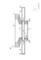
図1は、一実施形態の集積回路装置10の構造を示す平面図である。集積回路装置10は、樹脂フィルム1と、ICチップ2と、複数の配線3と、複数の配線4とを備えている。樹脂フィルム1は、柔軟性があり、折りたたむことが可能である(foldable)ように形成される。一実施形態では、樹脂フィルム1は、ポリイミドで形成される。配線3、4は、金属、例えば、銅(Cu)で形成される。
FIG. 1 is a plan view showing the structure of an integrated
ICチップ2は、樹脂フィルム1の表面に表面実装技術によって接合されている。一実施形態では、ICチップ2には、ASIC(application specific IC)、例えば、表示パネルを駆動する表示ドライバが集積化される。
The
配線3、4は、樹脂フィルム1の表面に接合されており、バンプ(図示されない)を介してICチップ2に形成された外部接続パッド(図示されない)に接続されている。配線3は、ICチップ2の-Y方向に位置する領域にX軸方向に並んで配置されており、配線4は、ICチップ2の+Y方向に位置する領域にX軸方向に並んで配置されている。ICチップ2は、複数の配線3に対して+Y方向にずれて位置しており、複数の配線4に対して-Y方向にずれて位置していることになる。
The
例えば、図1に図示されている構造は、Y軸方向に繰り返されてテープ状構造体を形成し、これがリールに巻回される。当該テープ状構造体は、所定の搬送方向(一実施形態では、Y軸方向に平行な方向)に搬送されながら、樹脂フィルム1に規定されたカットライン5で集積回路装置10が切断され、ICチップ2を含む部分6が、COFパッケージとして取り出される。樹脂フィルム1の両端には、搬送穴7が搬送方向に並んで配置されており、樹脂フィルム1は、搬送穴7を用いて当該搬送方向に搬送される。以下では、ICチップ2を含む部分6を、COFパッケージ6と記述することがある。取り出されたCOFパッケージ6が、最終的に携帯機器等の電子機器に実装される。
For example, the structure illustrated in FIG. 1 is repeated in the Y-axis direction to form a tape-like structure, which is wound on a reel. The tape-shaped structure is conveyed in a predetermined conveying direction (in one embodiment, a direction parallel to the Y-axis direction), and the
ICチップ2には、高速インターフェース2aが集積化されている。高速インターフェース2aの例としては、MIPI-DSI(mobile industry processor interface-digital serial interface)に準拠したインターフェース、TIA/EIA-644規格、TIA/EIA-644-A規格又はTIA/EIA-899規格に準拠したLVDS(low voltage differential signaling)インターフェースが挙げられる。符号3aは、配線3のうち、高速インターフェース2aに接続されているものを示している。
The
本実施形態では、電磁シールドを設置して配線3に印加されるノイズが低減される。詳細には、配線3が配置されている配線配置領域8に対して+X方向にずれた位置に保護パターン9が形成され、この保護パターン9が電磁シールドとして用いられる。保護パターン9は、樹脂フィルム1の表面に配線3、4を形成するプロセスにおいて同時に形成される。一実施形態では、樹脂フィルム1の表面に、銅薄膜等の導電体薄膜が形成され、その導電体薄膜がエッチングされることにより、配線3、4が形成される。保護パターン9は、このプロセスにおいて配線3、4と同時に形成される。この場合、保護パターン9は、配線3、4と同一の材料で形成されることになる。配線3、4が銅で形成される場合、保護パターン9も銅で形成される。
In this embodiment, noise applied to the
この集積回路装置10を電子機器に実装する場合、まず、樹脂フィルム1が配線3、4と共にカットライン5で切断され、図2に示すようにCOFパッケージ6が取り出される。
When mounting this
COFパッケージ6の樹脂フィルム1は、本体部分11と、本体部分11から+X方向に突出する突出部分12とを備えている。本体部分11にはICチップ2と配線3、4が形成されている。詳細には、本体部分11は、X軸に平行で互いに対向する一組のエッジ11a、11bを備えている。配線3のそれぞれは、その一端がエッジ11aに近接して位置しており、他端がICチップ2に接続されている。配線3は、エッジ11aに沿ってX軸方向に並んで配置されている。また、配線4のそれぞれは、その一端がエッジ11bに近接して位置しており、他端がICチップ2に接続されている。配線4は、エッジ11bに沿ってX軸方向に並んで配置されている。保護パターン9は、樹脂フィルム1の突出部分12に形成されている。
The
取り出されたCOFパッケージ6は、図3、図4に示すように、樹脂フィルム1の突出部分12がその根元の位置において折り曲げられる。図2では、突出部分12の根元の位置は、突出部分12が本体部分11に接合する位置として破線13で示されている。この折り曲げにより、図3に示すように、保護パターン9が配線3の少なくとも一部に対向する。このように、電子機器への実装時、保護パターン9が配線3に対向することにより、配線3の電磁シールドとして機能し、配線3に印加されるノイズが低減される。例えば、高速インターフェース2aに接続される配線3aに印加されるノイズの低減は、データ転送の信頼性の向上に有効である。
As shown in FIGS. 3 and 4, the removed
更に、保護パターン9は、樹脂フィルム1の廃棄される部分に形成されており、また、保護パターン9は、配線3、4を形成するプロセスにおいて同時に形成可能である。したがって、保護パターン9を配線3に対向するように樹脂フィルム1を折り曲げ、保護パターン9を電磁シールドとして使用することにより、低コストでノイズ低減を実現できる。
Furthermore, the
保護パターン9は、全ての配線3に対向してもよく、一部の配線3のみに対向していてもよい。一実施形態では、保護パターン9が、樹脂フィルム1が折り曲げられた後において、全ての配線3に対向していないが、配線3aを含む一部の配線3に対向するように配置されてもよい。
The
図5の一実施形態では、保護パターン9及び/又は配線3の少なくとも一部が、樹脂皮膜、例えば、ソルダーレジスト14で被覆されている。この樹脂皮膜は、保護パターン9と配線3との接触を防ぐ。この場合、例えば、配線3は、他の電子部品、例えば、フレキシブル配線基板(FPC:flexible printed circuit board)に接続される部分を除き、ソルダーレジスト14で被覆される。配線3の全体がソルダーレジスト14で被覆されてもよい。
In one embodiment of FIG. 5, at least part of the
保護パターン9及び樹脂フィルム1の突出部分12のX軸方向の許容される最大の幅寸法は、配線配置領域8のX軸方向の寸法に依存している。例えば、配線配置領域8に多くの配線3がX軸方向に並んで配置されている場合には、配線配置領域8のX軸方向の寸法が増大し、保護パターン9及び樹脂フィルム1の突出部分12のX軸方向の許容される最大の寸法は小さくなる。
The allowable maximum width dimension in the X-axis direction of the
保護パターン9及び樹脂フィルム1の突出部分12のX軸方向の許容される最大の寸法が小さい場合には、樹脂フィルム1を突出部分12の根元の位置で折り曲げても、保護パターン9が、電磁シールドを設けることが望ましい配線3を覆うように配置されないことが生じ得る。例えば、図6に図示されているように、高速インターフェース2aが、保護パターン9から離れて位置している場合には、樹脂フィルム1を突出部分12の根元の位置で折り曲げても、高速インターフェース2aに接続されている配線3aを保護パターン9で覆うことができない場合が生じ得る。
If the maximum allowable dimension in the X-axis direction of the
このような問題に対応するために、一実施形態では、電磁シールドを設けることが望ましい配線3が保護パターン9の近くの位置に配置される。例えば、高速インターフェース2a及び配線3aが、保護パターン9の近くの位置に配置される。一実施形態では、図7に示すように、ICチップ2について、ICチップ2のX軸方向における中心の位置を境界として第1半分部分2b及び第2半分部分2cを定義したとき、高速インターフェース2aは、保護パターン9に近い第1半分部分2bに位置している。これに伴い、高速インターフェース2aに接続される配線3aも保護パターン9の近くに配置され、保護パターン9が、配線3aの電磁シールドとして使用される。
In order to address such a problem, in one embodiment, the
他の実施形態では、図8及び図9に図示されているように、配線配置領域8の+X方向に位置する保護パターン91と、-X方向に位置する保護パターン92とが設けられる。カットライン5は、保護パターン91、92がCOFパッケージ6Aに含まれるように規定される。
In another embodiment, as shown in FIGS. 8 and 9, a
このCOFパッケージ6Aでは、樹脂フィルム1が、本体部分11と、本体部分11から+X方向に突出する突出部分121と、本体部分11から-X方向に突出する突出部分122とを備えている。保護パターン91、92は、樹脂フィルム1の突出部分121、122に形成されている。
In this
COFパッケージ6の電子機器への実装時、樹脂フィルム1が、突出部分121、122の根元の位置において折り曲げられ、図10に示すように配線3に対向する。図9では、突出部分121、122の根元の位置は、突出部分121、122が本体部分11に接合する位置として、それぞれ破線131、132で示されている。
When the
この構造では、図3の構造と比較して、より多くの配線3に電磁シールドを提供することができる。例えば、全ての配線3が、保護パターン91、92のうちの少なくとも一方に対向しており、これにより、全ての配線3についてノイズを低減することができる。
In this structure,
図11~図16Bは、突出部分12を2回折りする一実施形態を示す。
11-16B illustrate one embodiment in which the protruding
図11の集積回路装置10Bに設けられるカットライン5は、保護パターン9Bの形状に合わせた形状に規定される。保護パターン9Bは、図12に示すように、+X方向に延伸する第1パターン部分21と、第1パターン部分21の+X方向の端から+Y方向に突出する第2パターン部分22と、第2パターン部分22の第1パターン部分21から離れた位置(本実施形態では、第2パターン部分22の+Y方向の端)から-X方向に突出する第3パターン部分23とを有している。
The cut line 5 provided in the
図11の集積回路装置10Bをカットライン5で切断して得られるCOFパッケージ6Bは、図13に示すように、樹脂フィルム1が、本体部分11と、本体部分11から+X方向に突出する突出部分12Bを備えている。
A
突出部分12Bは、保護パターン9Bに対応する形状に構成されている。詳細には、図14に示すように、突出部分12Bは、本体部分11に接合し、本体部分11から+X方向に突出する第1部分31と、第1部分31の+X方向の端から+Y方向に突出する第2部分32と、第2部分32の第1部分31から離れた位置(本実施形態では、第2部分32の+Y方向の端)から-X方向に突出する第3部分33とを有している。
The projecting
保護パターン9Bは、図15に示すように、突出部分12Bの第1部分31に接合される部分と、第2部分32に接合される部分と、第3部分33に接合される部分とを有している。詳細には、保護パターン9Bの第1パターン部分21は、突出部分12Bの第1部分31に接合されている。保護パターン9Bの第2パターン部分22は、-Y方向に位置する端部が突出部分12Bの第1部分31に接合され、残部は、突出部分12Bの第2部分32に接合されている。保護パターン9Bの第3パターン部分23は、+X方向に位置する端部が突出部分12Bの第2部分32に接合され、残部は、突出部分12Bの第3部分33に接合されている。
As shown in FIG. 15, the
図13に戻り、COFパッケージ6Bが電子機器に実装される場合、樹脂フィルム1が2回折りされる。まず、樹脂フィルム1が、突出部分12Bの根元の位置において折り曲げられる。図13では、突出部分12Bの根元の位置が、突出部分12Bが本体部分11に接合する位置として破線13Bで示されている。図16Aは、この折り曲げ状態を示す。
Returning to FIG. 13, when the
更に、図16Bに図示されているように、樹脂フィルム1の突出部分12Bが、第2部分32と第3部分33とが接合する位置で、保護パターン9Bのうち第3部分33に接合されている部分が配線3に対向するように折り曲げられる。この状態では、保護パターン9Bの第3部分33の端は、突出部分12Bの第2部分32よりも突出部分12Bの根元の位置から離れており、保護パターン9Bの端から突出部分12Bの根元の位置までの距離を増大させることができる。このような構造によれば、保護パターン9Bを多くの配線3に、例えば突出部分12の根元から-X方向に離れた位置にある配線3にも対向させることができ、よって、多くの配線3に電磁シールドを設けることができる。
Furthermore, as shown in FIG. 16B, the projecting
樹脂フィルム1を3回以上折り畳むことで、保護パターンの端から突出部分の根元の位置までの距離を更に増大することも可能である。図17~図20Bは、樹脂フィルム1を3回折り畳む一実施形態を示す。
By folding the
図17に図示された集積回路装置10Cに設けられるカットライン5の形状も、図11と同様に、保護パターン9Cの形状に合わせて変更される。図18に示すように、保護パターン9Cは、+X方向に延伸する第1パターン部分21と、第1パターン部分21の+X方向の端から+Y方向に突出する第2パターン部分22と、第2パターン部分22の第1パターン部分21から離れた位置(本実施形態では、第2パターン部分22の+Y方向の端)から-X方向に突出する第3パターン部分23と、第3パターン部分23の-X方向の端から+Y方向に突出する第4パターン部分24と、第4パターン部分24の第3パターン部分23から離れた位置(本実施形態では、第4パターン部分24の+Y方向の端)から+X方向に突出する第5パターン部分25とを有している。
The shape of the cut line 5 provided in the
図17の集積回路装置10Cをカットライン5で切断して得られるCOFパッケージ6Cは、図19に示すように、樹脂フィルム1が、本体部分11と、本体部分11から+X方向に突出する突出部分12Cを備えている。
A
図20Aに図示されているように、突出部分12Cは、保護パターン9Cに対応する形状に構成されている。詳細には、突出部分12Cは、本体部分11に接合し、本体部分11から+X方向に突出する第1部分31と、第1部分31の+X方向の端から+Y方向に突出する第2部分32と、第2部分32の第1部分31から離れた位置(本実施形態では、第2部分32の+Y方向の端)から-X方向に突出する第3部分33と、第3部分33の-X方向の端から+Y方向に突出する第4部分34と、第4部分34の第3部分33から離れた位置(本実施形態では、第4部分34の+Y方向の端)から+X方向に突出する第5部分35とを有している。
As shown in FIG. 20A, the protruding
保護パターン9Cは、図20Bに示すように、突出部分12Cの第1~第5部分31~35にまたがって配置されており、突出部分12Cの第1~第5部分31~35に接合される部分を有している。
As shown in FIG. 20B, the
図19に戻り、COFパッケージ6Cが電子機器に実装される場合、樹脂フィルム1が3回折りされる。樹脂フィルム1が、突出部分12Cの根元の位置において折り曲げられる。更に、突出部分12Cが、第2部分32と第3部分33とが接合する位置において折り曲げられ、更に、突出部分12Cが、第4部分34と第5部分35とが接合する位置において折り曲げられる。このような構造では、保護パターン9Cの端から突出部分12Cの根元の位置までの距離を増大させることができ、保護パターン9Cを多くの配線3に対向させることができる。これは、多くの配線3に電磁シールドを設けることができることを意味している。
Returning to FIG. 19, when the
上述の実施形態では、保護パターン9、91、92、9B、9Cが、配線3の電磁シールドとして用いられるが、保護パターンは、ICチップ2の保護のために用いられてもよい。例えば、保護パターンは、ICチップ2の電磁シールドとしても使用可能である。また、保護パターンは、金属で形成されているので熱伝導性がよい。この性質を利用して、保護パターンは、ICチップ2が発生する熱を放出するための放熱体として利用可能である。また、保護パターンは、金属で形成されているので遮光性が高い。この性質を利用して、保護パターンは、ICチップ2への外光の入射を抑制する遮光体としても利用可能である。
Although the
図21に示す一実施形態では、保護パターン9が、ICチップ2が配置されているIC配置領域20に対して+X方向にずれた位置に形成されている。カットライン5の形状は、保護パターン9の位置に合わせて変更される。図21の構造では、保護パターン9は、ICチップ2へのノイズの印加を抑制するための電磁シールド、ICチップ2が発生する熱を放出するための放熱体、ICチップ2への外光の入射を抑制する遮光体の少なくとも一として用いられる。
In one embodiment shown in FIG. 21, the
図21の集積回路装置10Dをカットライン5で切断して得られるCOFパッケージ6Dは、図22に示すように、樹脂フィルム1が、本体部分11と、本体部分11から+X方向に突出する突出部分12とを備えており、保護パターン9は、樹脂フィルム1の突出部分12に接合される。
A
COFパッケージ6Dを電子機器に実装する場合、図22に示されている破線13にて、樹脂フィルム1が、保護パターン9がICチップ2に対向するように折り曲げられる。
When mounting the
図23は、折り曲げ後の状態を示し、ICチップ2が保護パターン9で覆われている。この実施形態では、保護パターン9が、ICチップ2の電磁シールド、ICチップ2が発生する熱を放出するための放熱体、ICチップ2への外光の入射を抑制する遮光体の少なくとも一として機能する。
FIG. 23 shows the state after bending, in which the
ICチップ2のうち保護パターンで覆われる部分を増大させるためには、図24に図示されているように、IC配置領域20の+X方向に位置する保護パターン91と、-X方向に位置する保護パターン92とを設けてもよい。カットライン5は、保護パターン91、92がCOFパッケージ6Eに含まれるように規定される。
In order to increase the portion of the IC chip 2 covered with the protective patterns, as shown in FIG. A
図24の集積回路装置10Eをカットライン5で切断して得られるCOFパッケージ6Eは、図25に示すように、樹脂フィルム1が、本体部分11と、本体部分11から+X方向に突出する突出部分121と、本体部分11から-X方向に突出する突出部分122とを備えている。保護パターン91、92は、それぞれ突出部分121、122に形成される。
A
COFパッケージ6Eを電子機器に実装する場合、樹脂フィルム1が、突出部分121、122の根元の位置において折り曲げられる。図25では、突出部分121、122の根元の位置が、突出部分121、122が本体部分11に接合する位置として、それぞれ破線131、132で示されている。
When mounting the
図26、図27に示すように、樹脂フィルム1は、保護パターン91、92がICチップ2に対向するように折り曲げられる。この構造では、図23の構造と比較して、ICチップ2の、より多くの部分を保護パターン91、92で被覆することができる。例えば、ICチップ2の全体が、保護パターン91、92のうちの少なくとも一方によって覆われており、これにより、ICチップ2の全体について、ICチップ2の電磁シールド、ICチップ2が発生する熱を放出するための放熱体、ICチップ2への外光の入射を抑制する遮光体のうちの少なくとも一の機能を提供することができる。なお、図5に図示されている構造と同様に、保護パターン91、92がICチップ2に接触することを防ぐためには、保護パターン91、92の少なくとも一部が樹脂皮膜、例えば、ソルダーレジストによって被覆されていてもよい。
As shown in FIGS. 26 and 27, the
保護パターン9、91、92、9B、9Cは、樹脂フィルム1が折り曲げられたときにICチップ2が配置されている領域及び配線3が配置されている領域の両方を覆うように形成されてもよい。図28に示す一実施形態では、保護パターン9が、ICチップ2と配線3とが配置されているIC配線配置領域30に対して+X方向にずれた位置に形成されている。カットライン5の形状は、保護パターン9の形状及び位置に合わせて変更される。この構造では、保護パターン9は、配線3へのノイズの印加を抑制するための電磁シールドとして用いられ、更に、ICチップ2へのノイズの印加を抑制するための電磁シールド、ICチップ2が発生する熱を放出するための放熱体、ICチップ2への外光の入射を抑制する遮光体の少なくとも一として用いられる。
The
図28の集積回路装置10Fをカットライン5で切断して得られるCOFパッケージ6Fは、図29に示すように、樹脂フィルム1が、本体部分11と、本体部分11から+X方向に突出する突出部分12とを備えており、保護パターン9は、樹脂フィルム1の突出部分12に接合される。
A
COFパッケージ6Fを電子機器に実装する場合、樹脂フィルム1が、保護パターン9がICチップ2及び配線3に対向するように折り曲げられる。図29では、突出部分12の根元の位置、即ち、樹脂フィルム1が折り曲げられる位置が破線13で示されている。
When mounting the
COFパッケージ6、6A~6Fの配線3がフレキシブル配線基板(FPC)に接合される場合には、保護パターン9、91、92、9B、9Cは、FPCに含まれる配線及び/又は回路素子へのノイズの印加を抑制する電磁シールドとして用いられてもよい。図25に図示されているCOFパッケージ6Eの保護パターン91、92が、FPC40に含まれる配線及び/又は回路素子へのノイズの印加を抑制する電磁シールドとして用いられる場合、図30に示すように、樹脂フィルム1が、突出部分121、122の根元の位置において折り曲げられる。図30では、突出部分121の根元の位置が、突出部分121、122が本体部分11に接合する位置として、それぞれ破線131、132で示されている。
When the
樹脂フィルム1は、図31、図32に示すように、保護パターン91、92がFPC40を挟んでICチップ2及び/又は配線3に対向するように折り曲げられる。このような構造では、保護パターン91、92が、FPC40の少なくとも一部を覆っており、FPC40に含まれる配線及び/又は回路素子へのノイズの印加を有効に抑制することができる。
As shown in FIGS. 31 and 32, the
一実施形態では、上述されたCOFパッケージにおいて、樹脂フィルム1が折り曲げられたときに突出部分12、121、122、12B、12Cを保持するための保持構造が樹脂フィルム1に形成される。
In one embodiment, in the COF package described above, a holding structure is formed in the
一実施形態では、樹脂フィルム1が折り曲げられたときに突出部分12、12B、12Cの先端が差し込まれる差込穴が樹脂フィルム1に形成されてもよい。突出部分12、12B、12Cは、その先端が差込穴に挿入されて保持される。このような構造は、特に、保護パターン9、9B、9C及び樹脂フィルム1の突出部分12、12B、12Cが、ICチップ2及び/又は配線3が配置される領域8、20、30に対して、特定方向にのみ配置されており、樹脂フィルム1が折り曲げられたときに突出部分の先端がICチップ2及び配線3の反対方向の位置に到達する場合に有効である。
In one embodiment, the
図33に示す一実施形態では、COFパッケージ6Gが、図19に図示されているCOFパッケージ6Cと同様に、3回折りに対応している。IC配線配置領域30に対して+X方向に位置する保護パターン9Cが樹脂フィルム1の突出部分12Cに形成されている。保護パターン9Cの構造は図18に図示されており、樹脂フィルム1の突出部分12Cの構造は図20A、20Bに図示されている。
In one embodiment shown in FIG. 33, the
COFパッケージ6Gでは、樹脂フィルム1に差込穴41が形成されている。差込穴41は、突出部分12Cの先端が挿入可能な形状を有している。
An
COFパッケージ6Gが電子機器に実装される場合、樹脂フィルム1が3回折りされる。詳細には、樹脂フィルム1が、突出部分12Cの根元の位置において折り曲げられ、突出部分12Cが、第2部分32と第3部分33とが接合する位置において折り曲げられ、更に、第4部分34と第5部分35とが接合する位置において折り曲げられる。突出部分12Cが、第4部分34と第5部分35とが接合する位置において折り曲げられた後、突出部分12Cの先端が差込穴41に挿入される。これにより、突出部分12Cの先端が保持される。
When the
突出部分の先端をより確実に保持するために、一実施形態では、突出部分の先端に、差込穴から突出部分の先端の抜けを防ぐための抜け止め構造が形成される。図34に示す一実施形態では、COFパッケージ6Gが、図33に図示されているCOFパッケージ6Gと類似した構造を有しているが、突出部分12Cの先端に抜け止め構造が形成されている。
In order to hold the tip of the projecting portion more securely, in one embodiment, the tip of the projecting portion is formed with a retaining structure for preventing the tip of the projecting portion from coming off from the insertion hole. In one embodiment shown in FIG. 34, a
突出部分12Cの先端に幅広部分42が形成されており、突出部分12Cの先端が差込穴41に差し込まれると、幅広部分42が差込穴41に引っかかることで突出部分12Cの先端が保持される。このような構造によれば、突出部分12Cの先端をより確実に保持することができる。
A
樹脂フィルム1が1回折りされる場合、2回折りされる場合、及び、4回又はそれ以上の回数折り曲げられる場合についても、樹脂フィルム1の突出部分の先端を差込穴で保持する構造は採用され得る。
When the
2つの保護パターン91、92及び2つの突出部分121、122が、ICチップ2及び/又は配線3が配置される領域8、20、30を挟んで互いに対向するように配置されている場合、一実施形態では、当該2つの突出部分が、樹脂フィルム1が折り曲げられたときに互いに嵌合して互いを保持するように構成されてもよい。
Two
図35に示す一実施形態では、COFパッケージ6Hは、突出部分121、122に、互いに嵌合可能な嵌合構造431、432がそれぞれ設けられている。嵌合構造431として突出部分121の-Y方向のエッジに設けられた凹部が形成されており、嵌合構造431は、第1のフックを構成している。嵌合構造432として突出部分122の+Y方向のエッジに設けられた凹部が形成されており、第2のフックを構成している。
In one embodiment shown in FIG. 35, the
COFパッケージ6Hが電子機器に実装される場合、樹脂フィルム1が、本体部分11と突出部分121、122とが接合する位置で折り曲げられる。更に、突出部分121、122にそれぞれに設けられた第1のフックと第2のフックが互いに引っ掛けられて嵌合構造431、432が互いに嵌合され、これにより、突出部分121、122が保持される。
When the
樹脂フィルム1を本体部分11と突出部分12、121、122、12B、12Cとが接合する位置で折り曲げることを容易にするためには、突出部分の本体部分と接合する部分を細く形成してもよい。
In order to facilitate bending of the
図36に示す一実施形態では、COFパッケージ6Jは、突出部分121、122の本体部分11と接合する部分が、Y軸方向における幅が細く形成されている。
In the embodiment shown in FIG. 36, in the
図37に示すように、突出部分121は、樹脂フィルム1の本体部分11と接合する根元部分12aと、根元部分12aに+X方向に接合する突出本体部分12bとを有している。根元部分12aのY軸方向の幅は、突出本体部分12bのY軸方向の幅よりも狭い。樹脂フィルム1の突出部分121の+Y方向の縁と-Y方向の縁にそれぞれ凹部15a、15bが形成されることで、根元部分12aのY軸方向の幅は、突出本体部分12bのY軸方向の幅より狭くされている。ただし、凹部15a、15bは、その一方のみが形成されてもよい。突出部分122についても、突出部分121と同様に構成されている。
As shown in FIG. 37, the protruding
このような構造によれば、樹脂フィルム1を本体部分11と突出部分121、122とが接合する位置で折り曲げることが容易になる。これは、工数の低減のために好ましい。なお、突出部分の本体部分と接合する部分を細く形成する構造は、他の実施形態についても適用可能である。
According to such a structure, it becomes easy to bend the
保護パターン9、91、92、9B、9Cの電磁シールドとしての機能を強化するためには、保護パターンが接地線と接続されてもよい。図38に示す一実施形態では、COFパッケージ6Jの保護パターン91が配線441によって接地線3bに接続され、保護パターン92が配線442によって接地線3cに接続される。このような構造によれば、保護パターン91、92が接地されるので、保護パターン91、92が電磁シールドとしてより有効に機能する。
In order to strengthen the function of the
上述の実施形態において、保護パターン9、91、92、9B、9Cは、様々な形態で実装され得る。図39に示す一実施形態では、保護パターン9の少なくとも一部が、樹脂皮膜、例えば、ソルダーレジスト45によって被覆される。このような構造によれば、保護パターン9が、ICチップ2や配線3と直接に接触することを防ぐことができる。
In the embodiments described above, the
また、図40に示すように、ソルダーレジスト45に開口45aが設けられてもよい。このような構造では、保護パターン9が開口45aを介して保護対象に直接に接触可能である。例えば、保護パターン9をICチップ2の放熱体として用いる場合には、保護パターン9がICチップ2に直接に接してもよい。
Further, as shown in FIG. 40, the solder resist 45 may be provided with
また、図41に図示されているように、保護パターン9、91、92、9B、9Cは、互いに分離され、特定方向に延伸する複数の導電体46の集合体として形成されてもよい。この場合も、図42に示すように、保護パターン9、91、92、9B、9Cの少なくとも一部が、樹脂皮膜、例えば、ソルダーレジスト45によって被覆されてもよい。
Also, as shown in FIG. 41, the
図43に示す一実施形態では、COFパッケージ6Kの樹脂フィルム1が、本体部分11と、本体部分11のICチップ2が配置されているIC配置領域20から+X方向に突出する突出部分12とを備えている。なお、図43は、COFパッケージ6Kを、樹脂フィルム1の裏面、即ち、ICチップ2が接合されている面と反対の面から見た図であり、このため、ICチップ2、配線3、4が点線により示されている。突出部分12は、ICチップ2に対して+X方向に位置している。
In one embodiment shown in FIG. 43, the
COFパッケージ6Kが電子機器に実装される場合、図44、図45に示すように、樹脂フィルム1が、突出部分12の根元の位置において、突出部分12が本体部分11の裏面11aに対向するように樹脂フィルム1が折り曲げられる。更に、スティフナー51がICチップ2に対向する位置において突出部分12に接合される。スティフナー51は、機械的力が作用したときにICチップ2の破損を防ぐために設けられる保護構造であり、一実施形態では、金属の板として形成される。一実施形態では、突出部分12が、本体部分11の裏面11aに接着材52により接着され、スティフナー51が、突出部分12の、本体部分11の裏面11aに接合する面と反対側の面に接着剤53により接着される。
When the
このような構造は、スティフナー51をCOFパッケージ6Kに搭載する工程で生じ得るダメージの影響を抑制するために有効である。例えば図46に図示されているような、本体部分11の裏面11cに金属製のスティフナー51が直接に接合される構造では、スティフナー51のエッジに形成されるバリ51aが、樹脂フィルム1を突き抜ける可能性がある。これは、電子機器の動作に影響するダメージを生じさせ得る。一方、図43~図45に示す本実施形態のCOFパッケージ6Kでは、スティフナー51のエッジに形成されるバリが樹脂フィルム1の本体部分11を貫通しにくく、電子機器の動作に影響するダメージの発生を抑制できる。
Such a structure is effective in suppressing the influence of damage that may occur in the process of mounting the
図47に示すように、突出部分12に開口54が設けられてもよい。この場合、図48、図49に示すように、突出部分12の根元の位置において樹脂フィルム1が折り曲げられ、スティフナー51は、開口54を塞ぐように突出部分12に接合される。開口54を設けることは、スティフナー51の位置合わせを容易化し、スティフナー51のズレを抑制するために有効である。
As shown in FIG. 47,
図50に示す一実施形態では、COFパッケージ6Lの樹脂フィルム1が、本体部分11と、本体部分11のIC配置領域20から+X方向に突出する突出部分121と、IC配置領域20から-X方向に突出する突出部分122とを備えている。なお、図47は、COFパッケージ6Lを、樹脂フィルム1の裏面から見た図である。
In one embodiment shown in FIG. 50, the resin film 1 of the
COFパッケージ6Lが電子機器に実装される場合、図51~図53に示すように、突出部分121、122が本体部分11の裏面11cに向けて折り曲げられ、スティフナー51が突出部分12に接合される。樹脂フィルム1は、突出部分12の根元の位置において、突出部分12が本体部分11の裏面11aに対向するように折り曲げられ、更に、スティフナー51が突出部分121、122に接合される。
When the
このような構造も、スティフナー51をCOFパッケージ6Kに搭載する工程で生じ得るダメージの影響を抑制するために有効である。加えて、2つの突出部分121、122が設けられる本実施形態のCOFパッケージ6Lの構造は、突出部分121、122のX軸方向の許容される最大の寸法が小さい場合に有効である。
Such a structure is also effective in suppressing the influence of damage that may occur in the process of mounting the
なお、図43~図45に示す実施形態、図47~図49に示す実施形態及び図50及び図51に示す実施形態においても、樹脂フィルム1を本体部分11と突出部分12、121、122とが接合する位置で折り曲げることを容易にするために、突出部分の本体部分と接合する部分を細く形成してもよい。 43 to 45, the embodiment shown in FIGS. 47 to 49 , and the embodiments shown in FIGS. In order to facilitate bending at the position where 2 are joined, the portion of the protruding portion that joins with the body portion may be formed thin.
例えば図54に示す一実施形態のCOFパッケージ6Mでは、突出部分12の本体部分11と接合する部分が、Y軸方向における幅が細く形成されている。突出部分12は、樹脂フィルム1の本体部分11と接合する根元部分12aと、根元部分12aに+X方向に接合する突出本体部分12bとを有している。根元部分12aのY軸方向の幅は、突出本体部分12bのY軸方向の幅よりも狭い。樹脂フィルム1の突出部分12の+Y方向の縁と-Y方向の縁にそれぞれ凹部15a、15bが形成されることで、根元部分12aのY軸方向の幅は、突出本体部分12bのY軸方向の幅より狭くされている。ただし、凹部15a、15bは、その一方のみが形成されてもよい。このような構造によれば、樹脂フィルム1を本体部分11と突出部分12とが接合する位置で折り曲げることが容易になる。
For example, in the
以上には、本開示の実施形態が具体的に記述されているが、本開示が種々の変更と共に実施され得ることは、当業者には理解されよう。上記の実施形態は、技術的な矛盾がない限り、組み合わせて実施され得る。 Although the embodiments of the present disclosure have been specifically described above, those skilled in the art will appreciate that the present disclosure may be practiced with various modifications. The above-described embodiments can be implemented in combination as long as there is no technical contradiction.
10、10A-10F:集積回路装置
1 :樹脂フィルム
2 :ICチップ
2a :高速インターフェース
2b :第1半分部分
2c :第2半分部分
3 :配線
3a :配線
3b :接地線
3c :接地線
4 :配線
5 :カットライン
6、6A-6M:COFパッケージ
7 :搬送穴
8 :配線配置領域
9、91、92、9B、9C:保護パターン
11 :本体部分
11a :エッジ
11b :エッジ
12、121、122、12B、12C:突出部分
12a :根元部分
12b :突出本体部分
13、131、132、13B :破線
14 :ソルダーレジスト
15a、15b:凹部
20 :IC配置領域
21 :第1パターン部分
22 :第2パターン部分
23 :第3パターン部分
24 :第4パターン部分
25 :第5パターン部分
30 :IC配線配置領域
31 :第1部分
32 :第2部分
33 :第3部分
34 :第4部分
35 :第5部分
40 :FPC
41 :差込穴
42 :幅広部分
431、432:嵌合構造
441、442:配線
45 :ソルダーレジスト
45a :開口
46 :導電体
51 :スティフナー
52、53:接着剤
54 :開口
100 :集積回路装置
101 :樹脂フィルム
102 :ICチップ
103 :配線
104 :配線
105 :カットライン
106 :部分
107 :搬送穴
10, 10A-10F: integrated circuit device 1: resin film 2:
41 : Insertion hole 42 : Wide portion 43 1 , 43 2 : Fitting structure 44 1 , 44 2 : Wiring 45 : Solder resist 45a : Opening 46 : Conductor 51 :
Claims (6)
前記フィルムの表面に接合された複数の配線と、
前記フィルムの前記表面に接合され、前前記複数の配線に電気的に接続されたICチップと、
前記フィルムの前記表面に接合され、前記ICチップ及び/又は前記複数の配線が配置されている配置領域に対してずれて位置しており、前記複数の配線と同一の材料で形成された第1保護パターン
とを備え、
前記第1保護パターンが、
第1端から第2端に第1方向に延伸する第1パターン部分と、
前記第1パターン部分の前記第2端から前記第1方向と垂直な方向に突出する第2パターン部分と、
前記第2パターン部分の前記第1パターン部分から離れた位置から前記第1方向と反対の第2方向に突出する第3パターン部分と、
を備える
集積回路装置。 flexible film,
a plurality of wirings bonded to the surface of the film;
an IC chip bonded to the surface of the film and electrically connected to the plurality of wirings;
A first film, which is bonded to the surface of the film, is offset from an arrangement region where the IC chip and/or the plurality of wirings are arranged, and is formed of the same material as the plurality of wirings. with a protective pattern and
The first protective pattern is
a first pattern portion extending in a first direction from a first end to a second end;
a second pattern portion protruding from the second end of the first pattern portion in a direction perpendicular to the first direction;
a third pattern portion projecting in a second direction opposite to the first direction from a position of the second pattern portion spaced apart from the first pattern portion;
have
Integrated circuit device.
前記フィルムは、
前記複数の配線と前記ICチップとが接合された本体部分と、
前記本体部分から第1方向に突出する第1突出部分
とを備え、
前記第1保護パターンは、前記フィルムの前記第1突出部分に接合された
集積回路装置。 The integrated circuit device according to claim 1,
The film is
a body portion where the plurality of wirings and the IC chip are joined;
a first projecting portion projecting in a first direction from the body portion;
The integrated circuit device, wherein the first protective pattern is bonded to the first projecting portion of the film.
前記複数の配線が、接地線を備え、
前記第1保護パターンが前記接地線に接続された
集積回路装置。 The integrated circuit device according to claim 1 or 2 ,
wherein the plurality of wires comprises a ground wire;
An integrated circuit device, wherein the first protective pattern is connected to the ground line.
前記フィルムの表面に接合された複数の配線と、
前記フィルムの前記表面に接合され、前記複数の配線に電気的に接続されたICチップと、
前記複数の配線と同一の材料で形成された第1保護パターンと、
を備え、
前記フィルムは、
前記複数の配線と前記ICチップとが接合された本体部分と、
前記本体部分から突出する第1突出部分
とを備え、
前記第1保護パターンは、前記フィルムの前記第1突出部分に接合され、
前記第1保護パターンが、
第1端から第2端に第1方向に延伸する第1パターン部分と、
前記第1パターン部分の前記第2端から前記第1方向と垂直な方向に突出する第2パターン部分と、
前記第2パターン部分の前記第1パターン部分から離れた位置から前記第1方向と反対の第2方向に突出する第3パターン部分と、
を備え、
前記フィルムが、前記第1突出部分及び前記第1保護パターンが前記本体部分に対向するように折り曲げられた
電子機器。 flexible film,
a plurality of wirings bonded to the surface of the film;
an IC chip bonded to the surface of the film and electrically connected to the plurality of wirings ;
a first protection pattern formed of the same material as the plurality of wirings;
with
The film is
a body portion where the plurality of wirings and the IC chip are joined;
a first protruding portion protruding from the body portion;
the first protective pattern is bonded to the first protruding portion of the film;
The first protective pattern is
a first pattern portion extending in a first direction from a first end to a second end;
a second pattern portion protruding from the second end of the first pattern portion in a direction perpendicular to the first direction;
a third pattern portion projecting in a second direction opposite to the first direction from a position of the second pattern portion spaced apart from the first pattern portion;
with
The electronic device, wherein the film is folded such that the first projecting portion and the first protective pattern face the body portion.
前記フィルムの表面に接合された複数の配線と、
前記フィルムの前記表面に接合され、前記複数の配線に電気的に接続されたICチップと、
前記複数の配線と同一の材料で形成された第1保護パターンと、
フレキシブル配線基板
を備え、
前記フィルムは、
前記複数の配線と前記ICチップとが接合された本体部分と、
前記本体部分から突出する第1突出部分
とを備え、
前記第1保護パターンは、前記フィルムの前記第1突出部分に接合され、
前記フレキシブル配線基板が、前記フィルムの前記本体部分に対向するように配置され、
前記フィルムが、前記第1突出部分及び前記第1保護パターンが前記フレキシブル配線基板を挟んで前記少なくとも一部の配線及び/又は前記ICチップに対向するように折り曲げられた
電子機器。 flexible film,
a plurality of wirings bonded to the surface of the film;
an IC chip bonded to the surface of the film and electrically connected to the plurality of wirings;
a first protection pattern formed of the same material as the plurality of wirings;
Flexible wiring board
with
The film is
a body portion where the plurality of wirings and the IC chip are joined;
A first protruding portion protruding from the body portion
and
the first protective pattern is bonded to the first protruding portion of the film;
The flexible wiring board is arranged to face the body portion of the film ,
The electronic device, wherein the film is folded such that the first protruding portion and the first protective pattern face the at least part of the wiring and/or the IC chip with the flexible wiring substrate interposed therebetween.
前記フィルムの表面に接合された複数の配線と、
前記フィルムの前記表面に接合され、前記複数の配線に電気的に接続されたICチップと、
スティフナーと、
を備え、
前記フィルムは、
前記複数の配線と前記ICチップとが接合された本体部分と、
前記本体部分から突出する第1突出部分
とを備え、
前記フィルムが、前記第1突出部分が前記本体部分に対向するように折り曲げられ、
前記スティフナーが、前記第1突出部分に前記ICチップと対向するように接合された
電子機器。 flexible film,
a plurality of wirings bonded to the surface of the film;
an IC chip bonded to the surface of the film and electrically connected to the plurality of wirings;
a stiffener;
with
The film is
a body portion where the plurality of wirings and the IC chip are joined;
A first protruding portion protruding from the body portion
and
the film is folded such that the first protruding portion faces the body portion;
An electronic device , wherein the stiffener is joined to the first projecting portion so as to face the IC chip.
Priority Applications (3)
| Application Number | Priority Date | Filing Date | Title |
|---|---|---|---|
| PCT/JP2018/036904 WO2019069935A1 (en) | 2017-10-06 | 2018-10-02 | Integrated circuit device and electronic equipment |
| US16/753,758 US11171111B2 (en) | 2017-10-06 | 2018-10-02 | Integrated circuit device and electronic device |
| CN201880064882.4A CN111448650B (en) | 2017-10-06 | 2018-10-02 | Integrated circuit devices and electronic devices |
Applications Claiming Priority (2)
| Application Number | Priority Date | Filing Date | Title |
|---|---|---|---|
| JP2017195938 | 2017-10-06 | ||
| JP2017195938 | 2017-10-06 |
Publications (3)
| Publication Number | Publication Date |
|---|---|
| JP2019071401A JP2019071401A (en) | 2019-05-09 |
| JP2019071401A5 JP2019071401A5 (en) | 2021-02-25 |
| JP7108415B2 true JP7108415B2 (en) | 2022-07-28 |
Family
ID=66440735
Family Applications (1)
| Application Number | Title | Priority Date | Filing Date |
|---|---|---|---|
| JP2018010029A Active JP7108415B2 (en) | 2017-10-06 | 2018-01-24 | Integrated circuit devices and electronic equipment |
Country Status (3)
| Country | Link |
|---|---|
| US (1) | US11171111B2 (en) |
| JP (1) | JP7108415B2 (en) |
| CN (1) | CN111448650B (en) |
Families Citing this family (1)
| Publication number | Priority date | Publication date | Assignee | Title |
|---|---|---|---|---|
| KR20210112432A (en) | 2020-03-04 | 2021-09-15 | 삼성디스플레이 주식회사 | Display device |
Citations (5)
| Publication number | Priority date | Publication date | Assignee | Title |
|---|---|---|---|---|
| JP2000077482A (en) | 1998-08-27 | 2000-03-14 | Sharp Corp | Tape carrier package |
| JP2001358245A (en) | 2000-06-14 | 2001-12-26 | Seiko Epson Corp | Wiring board manufacturing method, semiconductor device and manufacturing method thereof, circuit board, and electronic equipment |
| JP2007157929A (en) | 2005-12-02 | 2007-06-21 | Nitto Denko Corp | Printed circuit board |
| JP2008091797A (en) | 2006-10-04 | 2008-04-17 | Olympus Corp | Jointing device of flexible substrate |
| JP2008159873A (en) | 2006-12-25 | 2008-07-10 | Epson Imaging Devices Corp | Flexible printed wiring board, manufacturing method thereof, electro-optical device, and electronic apparatus |
Family Cites Families (9)
| Publication number | Priority date | Publication date | Assignee | Title |
|---|---|---|---|---|
| JPS58105165U (en) * | 1982-01-09 | 1983-07-18 | キヤノン株式会社 | flexible printed board |
| JPS62269399A (en) * | 1986-05-19 | 1987-11-21 | 松下電器産業株式会社 | Shielding device |
| JPH04263495A (en) * | 1991-02-18 | 1992-09-18 | Ibiden Co Ltd | Flexible wiring board |
| JP3234743B2 (en) * | 1995-05-30 | 2001-12-04 | シャープ株式会社 | Semiconductor component mounting type flexible printed circuit board |
| JP3550253B2 (en) * | 1996-07-23 | 2004-08-04 | 株式会社東芝 | Electronics |
| US7777329B2 (en) * | 2006-07-27 | 2010-08-17 | International Business Machines Corporation | Heatsink apparatus for applying a specified compressive force to an integrated circuit device |
| KR101319592B1 (en) * | 2006-07-31 | 2013-10-16 | 삼성디스플레이 주식회사 | Multi-layer flexible film package and liquid crystal display device having the same |
| TWI337402B (en) * | 2007-01-03 | 2011-02-11 | Chipmos Technologies Inc | Semiconductor packaging substrate improving capability of electrostatic dissipation |
| US9953952B2 (en) * | 2008-08-20 | 2018-04-24 | Infineon Technologies Ag | Semiconductor device having a sealant layer including carbon directly contact the chip and the carrier |
-
2018
- 2018-01-24 JP JP2018010029A patent/JP7108415B2/en active Active
- 2018-10-02 CN CN201880064882.4A patent/CN111448650B/en active Active
- 2018-10-02 US US16/753,758 patent/US11171111B2/en active Active
Patent Citations (5)
| Publication number | Priority date | Publication date | Assignee | Title |
|---|---|---|---|---|
| JP2000077482A (en) | 1998-08-27 | 2000-03-14 | Sharp Corp | Tape carrier package |
| JP2001358245A (en) | 2000-06-14 | 2001-12-26 | Seiko Epson Corp | Wiring board manufacturing method, semiconductor device and manufacturing method thereof, circuit board, and electronic equipment |
| JP2007157929A (en) | 2005-12-02 | 2007-06-21 | Nitto Denko Corp | Printed circuit board |
| JP2008091797A (en) | 2006-10-04 | 2008-04-17 | Olympus Corp | Jointing device of flexible substrate |
| JP2008159873A (en) | 2006-12-25 | 2008-07-10 | Epson Imaging Devices Corp | Flexible printed wiring board, manufacturing method thereof, electro-optical device, and electronic apparatus |
Also Published As
| Publication number | Publication date |
|---|---|
| US20200279828A1 (en) | 2020-09-03 |
| US11171111B2 (en) | 2021-11-09 |
| CN111448650A (en) | 2020-07-24 |
| CN111448650B (en) | 2024-11-12 |
| JP2019071401A (en) | 2019-05-09 |
Similar Documents
| Publication | Publication Date | Title |
|---|---|---|
| KR100765478B1 (en) | Tape wiring board with holes formed therein, tape package and flat panel display using the same | |
| CN101971716B (en) | 10g xfp compliant pcb | |
| CN101616536B (en) | Circuit board with electrostatic discharge protection and liquid crystal module and electronic device using it | |
| US8975762B2 (en) | Semiconductor device | |
| CN106898587A (en) | Heat dissipation packaging structure | |
| US9112310B2 (en) | Spark gap for high-speed cable connectors | |
| KR20140125673A (en) | Cof package and display device including the same | |
| KR100658442B1 (en) | Heat dissipation tape package and flat panel display using the same | |
| JP7108415B2 (en) | Integrated circuit devices and electronic equipment | |
| TW201342011A (en) | Electronic apparatus | |
| CN110290632B (en) | Electronic device for electrostatic discharge protection | |
| US9538661B2 (en) | Electronic device module including a printed circuit | |
| US20070257337A1 (en) | Shield substrate, semiconductor package, and semiconductor device | |
| WO2019069935A1 (en) | Integrated circuit device and electronic equipment | |
| JP5878611B2 (en) | Semiconductor device | |
| US12003047B2 (en) | Wiring substrate and information processing device | |
| JP5657767B2 (en) | Semiconductor device | |
| JP2018085522A (en) | Semiconductor device | |
| US7663208B2 (en) | Punch type substrate strip | |
| JP7318055B2 (en) | semiconductor equipment | |
| CN110072328A (en) | A kind of flexible circuit board | |
| CN220629951U (en) | Display module and display device | |
| JP6870043B2 (en) | Semiconductor device | |
| JP5405679B2 (en) | Semiconductor device | |
| KR20250026434A (en) | Chip on film package |
Legal Events
| Date | Code | Title | Description |
|---|---|---|---|
| RD04 | Notification of resignation of power of attorney |
Free format text: JAPANESE INTERMEDIATE CODE: A7424 Effective date: 20191209 |
|
| A711 | Notification of change in applicant |
Free format text: JAPANESE INTERMEDIATE CODE: A711 Effective date: 20200310 |
|
| A521 | Request for written amendment filed |
Free format text: JAPANESE INTERMEDIATE CODE: A821 Effective date: 20200310 |
|
| A521 | Request for written amendment filed |
Free format text: JAPANESE INTERMEDIATE CODE: A523 Effective date: 20210113 |
|
| A621 | Written request for application examination |
Free format text: JAPANESE INTERMEDIATE CODE: A621 Effective date: 20210113 |
|
| A131 | Notification of reasons for refusal |
Free format text: JAPANESE INTERMEDIATE CODE: A131 Effective date: 20220105 |
|
| A521 | Request for written amendment filed |
Free format text: JAPANESE INTERMEDIATE CODE: A523 Effective date: 20220330 |
|
| TRDD | Decision of grant or rejection written | ||
| A01 | Written decision to grant a patent or to grant a registration (utility model) |
Free format text: JAPANESE INTERMEDIATE CODE: A01 Effective date: 20220622 |
|
| A61 | First payment of annual fees (during grant procedure) |
Free format text: JAPANESE INTERMEDIATE CODE: A61 Effective date: 20220715 |
|
| R150 | Certificate of patent or registration of utility model |
Ref document number: 7108415 Country of ref document: JP Free format text: JAPANESE INTERMEDIATE CODE: R150 |