JP7085417B2 - 半導体装置 - Google Patents
半導体装置 Download PDFInfo
- Publication number
- JP7085417B2 JP7085417B2 JP2018119615A JP2018119615A JP7085417B2 JP 7085417 B2 JP7085417 B2 JP 7085417B2 JP 2018119615 A JP2018119615 A JP 2018119615A JP 2018119615 A JP2018119615 A JP 2018119615A JP 7085417 B2 JP7085417 B2 JP 7085417B2
- Authority
- JP
- Japan
- Prior art keywords
- wiring
- dummy
- semiconductor device
- corner
- view
- Prior art date
- Legal status (The legal status is an assumption and is not a legal conclusion. Google has not performed a legal analysis and makes no representation as to the accuracy of the status listed.)
- Active
Links
- 239000004065 semiconductor Substances 0.000 title claims description 165
- 239000004020 conductor Substances 0.000 claims description 93
- 230000001154 acute effect Effects 0.000 claims description 27
- 239000000758 substrate Substances 0.000 claims description 24
- 239000010410 layer Substances 0.000 description 73
- 230000004048 modification Effects 0.000 description 54
- 238000012986 modification Methods 0.000 description 54
- 230000035882 stress Effects 0.000 description 40
- 208000022859 zygodactyly type 1 Diseases 0.000 description 29
- 230000015572 biosynthetic process Effects 0.000 description 28
- 238000004519 manufacturing process Methods 0.000 description 27
- 238000000034 method Methods 0.000 description 17
- 238000005530 etching Methods 0.000 description 16
- 208000018670 synpolydactyly type 1 Diseases 0.000 description 13
- 239000011229 interlayer Substances 0.000 description 11
- 238000000926 separation method Methods 0.000 description 10
- VYPSYNLAJGMNEJ-UHFFFAOYSA-N Silicium dioxide Chemical compound O=[Si]=O VYPSYNLAJGMNEJ-UHFFFAOYSA-N 0.000 description 9
- 230000007547 defect Effects 0.000 description 9
- 229910052814 silicon oxide Inorganic materials 0.000 description 9
- 229920002120 photoresistant polymer Polymers 0.000 description 8
- 230000008646 thermal stress Effects 0.000 description 6
- 229910052782 aluminium Inorganic materials 0.000 description 5
- XAGFODPZIPBFFR-UHFFFAOYSA-N aluminium Chemical compound [Al] XAGFODPZIPBFFR-UHFFFAOYSA-N 0.000 description 5
- 229910052751 metal Inorganic materials 0.000 description 5
- 239000002184 metal Substances 0.000 description 5
- 230000001681 protective effect Effects 0.000 description 5
- 208000018985 Synpolydactyly type 3 Diseases 0.000 description 4
- 208000011913 Zygodactyly type 2 Diseases 0.000 description 4
- 208000014635 Zygodactyly type 3 Diseases 0.000 description 4
- 208000025793 synpolydactyly type 2 Diseases 0.000 description 4
- WFKWXMTUELFFGS-UHFFFAOYSA-N tungsten Chemical compound [W] WFKWXMTUELFFGS-UHFFFAOYSA-N 0.000 description 4
- 229910052721 tungsten Inorganic materials 0.000 description 4
- 239000010937 tungsten Substances 0.000 description 4
- XUIMIQQOPSSXEZ-UHFFFAOYSA-N Silicon Chemical compound [Si] XUIMIQQOPSSXEZ-UHFFFAOYSA-N 0.000 description 3
- 238000001312 dry etching Methods 0.000 description 3
- 239000012528 membrane Substances 0.000 description 3
- 238000000206 photolithography Methods 0.000 description 3
- 229910021420 polycrystalline silicon Inorganic materials 0.000 description 3
- 229920005591 polysilicon Polymers 0.000 description 3
- 229910052710 silicon Inorganic materials 0.000 description 3
- 239000010703 silicon Substances 0.000 description 3
- RTAQQCXQSZGOHL-UHFFFAOYSA-N Titanium Chemical compound [Ti] RTAQQCXQSZGOHL-UHFFFAOYSA-N 0.000 description 2
- NRTOMJZYCJJWKI-UHFFFAOYSA-N Titanium nitride Chemical compound [Ti]#N NRTOMJZYCJJWKI-UHFFFAOYSA-N 0.000 description 2
- 238000004380 ashing Methods 0.000 description 2
- 238000005229 chemical vapour deposition Methods 0.000 description 2
- 239000012535 impurity Substances 0.000 description 2
- 238000004544 sputter deposition Methods 0.000 description 2
- 239000010936 titanium Substances 0.000 description 2
- 229910052719 titanium Inorganic materials 0.000 description 2
- 239000000470 constituent Substances 0.000 description 1
- 230000002950 deficient Effects 0.000 description 1
- 239000002019 doping agent Substances 0.000 description 1
- 230000012447 hatching Effects 0.000 description 1
- 238000010438 heat treatment Methods 0.000 description 1
- 230000001939 inductive effect Effects 0.000 description 1
- 238000009413 insulation Methods 0.000 description 1
- 239000000463 material Substances 0.000 description 1
- 238000005457 optimization Methods 0.000 description 1
- 238000007254 oxidation reaction Methods 0.000 description 1
- 238000004088 simulation Methods 0.000 description 1
Images


Classifications
-
- H—ELECTRICITY
- H01—ELECTRIC ELEMENTS
- H01L—SEMICONDUCTOR DEVICES NOT COVERED BY CLASS H10
- H01L23/00—Details of semiconductor or other solid state devices
- H01L23/562—Protection against mechanical damage
-
- H—ELECTRICITY
- H01—ELECTRIC ELEMENTS
- H01L—SEMICONDUCTOR DEVICES NOT COVERED BY CLASS H10
- H01L21/00—Processes or apparatus adapted for the manufacture or treatment of semiconductor or solid state devices or of parts thereof
- H01L21/70—Manufacture or treatment of devices consisting of a plurality of solid state components formed in or on a common substrate or of parts thereof; Manufacture of integrated circuit devices or of parts thereof
- H01L21/71—Manufacture of specific parts of devices defined in group H01L21/70
- H01L21/768—Applying interconnections to be used for carrying current between separate components within a device comprising conductors and dielectrics
- H01L21/76838—Applying interconnections to be used for carrying current between separate components within a device comprising conductors and dielectrics characterised by the formation and the after-treatment of the conductors
- H01L21/76885—By forming conductive members before deposition of protective insulating material, e.g. pillars, studs
-
- H—ELECTRICITY
- H01—ELECTRIC ELEMENTS
- H01L—SEMICONDUCTOR DEVICES NOT COVERED BY CLASS H10
- H01L23/00—Details of semiconductor or other solid state devices
- H01L23/52—Arrangements for conducting electric current within the device in operation from one component to another, i.e. interconnections, e.g. wires, lead frames
- H01L23/522—Arrangements for conducting electric current within the device in operation from one component to another, i.e. interconnections, e.g. wires, lead frames including external interconnections consisting of a multilayer structure of conductive and insulating layers inseparably formed on the semiconductor body
- H01L23/5226—Via connections in a multilevel interconnection structure
-
- H—ELECTRICITY
- H01—ELECTRIC ELEMENTS
- H01L—SEMICONDUCTOR DEVICES NOT COVERED BY CLASS H10
- H01L23/00—Details of semiconductor or other solid state devices
- H01L23/52—Arrangements for conducting electric current within the device in operation from one component to another, i.e. interconnections, e.g. wires, lead frames
- H01L23/522—Arrangements for conducting electric current within the device in operation from one component to another, i.e. interconnections, e.g. wires, lead frames including external interconnections consisting of a multilayer structure of conductive and insulating layers inseparably formed on the semiconductor body
- H01L23/528—Layout of the interconnection structure
- H01L23/5283—Cross-sectional geometry
-
- H—ELECTRICITY
- H01—ELECTRIC ELEMENTS
- H01L—SEMICONDUCTOR DEVICES NOT COVERED BY CLASS H10
- H01L2225/00—Details relating to assemblies covered by the group H01L25/00 but not provided for in its subgroups
- H01L2225/03—All the devices being of a type provided for in the same main group of the same subclass of class H10, e.g. assemblies of rectifier diodes
- H01L2225/04—All the devices being of a type provided for in the same main group of the same subclass of class H10, e.g. assemblies of rectifier diodes the devices not having separate containers
- H01L2225/065—All the devices being of a type provided for in the same main group of the same subclass of class H10
- H01L2225/06503—Stacked arrangements of devices
- H01L2225/06541—Conductive via connections through the device, e.g. vertical interconnects, through silicon via [TSV]
- H01L2225/06544—Design considerations for via connections, e.g. geometry or layout
Landscapes
- Physics & Mathematics (AREA)
- Engineering & Computer Science (AREA)
- Condensed Matter Physics & Semiconductors (AREA)
- General Physics & Mathematics (AREA)
- Computer Hardware Design (AREA)
- Microelectronics & Electronic Packaging (AREA)
- Power Engineering (AREA)
- Geometry (AREA)
- Manufacturing & Machinery (AREA)
- Internal Circuitry In Semiconductor Integrated Circuit Devices (AREA)
Description
以下の実施の形態では特に必要なとき以外は同一または同様な部分の説明を原則として繰り返さない。
<半導体装置の構造について>
一実施の形態による半導体装置の構成を、図1~図2を用いて説明する。図1は、実施の形態1の半導体装置SD1aの拡大平面図である。図2は、実施の形態1の半導体装置SD1aにおいて、(a)は図1のA-A線に沿って切断した構造を示す要部断面図、(b)は図1のB-B線に沿って切断した構造を示す要部断面図である。
実施の形態1の半導体装置SD1aの製造方法について、図3~図7を用いて工程順に説明する。図3(a)~図7(a)は、実施の形態1の半導体装置SD1aの製造工程中の要部断面図において、図1のA-A線に相当する線に沿って切断した構造を示す要部断面図である。図3(b)~図7(b)は、実施の形態1の半導体装置SD1aの製造工程中の要部断面図において、図1のB-B線に相当する線に沿って切断した構造を示す要部断面図である。
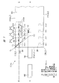
以下、本発明者が検討した検討例の半導体装置の構成について説明する。図8は、検討例の半導体装置SD101の拡大平面図である。
以下、実施の形態1の主要な特徴について説明する。図11は、実施の形態1の半導体装置SD1aにおいて、図1のB-B線に沿って切断した構造における第1ビアと第2ビアとの位置関係を示す要部断面図である。図12は、実施の形態1の半導体装置SD1aにおいて、図1のB-B線に沿って切断した構造を示す要部断面図である。
ここで、ダミービアDV1の配置の最適化について検討する。図13は、実施の形態1の半導体装置SD1aにおいて、平面視におけるビアV2とダミービアDV1との位置関係を示す拡大平面図である。図14は、実施の形態1の半導体装置SD1aにおいて、平面視におけるダミービアDV1の位置とダミービアDV1の底部にかかる応力との関係を示すグラフである。図15は、実施の形態1の半導体装置SD1aにおいて、平面視におけるダミービアDV1の位置と角部CIにかかる応力との関係を示すグラフである。
上記実施の形態1の第1の変形例(以下、変形例1)の半導体装置について説明する。図16は、変形例1の半導体装置SD1bを示す拡大平面図である。
上記実施の形態1の第2の変形例(以下、変形例2)の半導体装置について説明する。図17は、変形例2の半導体装置SD1cを示す拡大平面図である。
実施の形態2の半導体装置について説明する。図18は、実施の形態2の半導体装置SD2aを示す拡大平面図である。図19は、実施の形態2の半導体装置SD2aにおいて、図18のB-B線に沿って切断した構造を示す要部断面図である。
上記実施の形態2の第1の変形例(以下、変形例3)の半導体装置について説明する。図20は、変形例3の半導体装置SD2bを示す拡大平面図である。
上記実施の形態2の第2の変形例(以下、変形例4)の半導体装置について説明する。図21は、変形例4の半導体装置SD2cを示す拡大平面図である。
実施の形態3の半導体装置について説明する。図22は、実施の形態3の半導体装置SD3aを示す拡大平面図である。
上記実施の形態3の第1の変形例(以下、変形例5)の半導体装置について説明する。図23は、変形例5の半導体装置SD3bを示す拡大平面図である。
上記実施の形態3の第2の変形例(以下、変形例6)の半導体装置について説明する。図24は、変形例6の半導体装置SD3cを示す拡大平面図である。
(a)基板を準備する工程、
(b)前記基板上に第1絶縁膜を形成する工程、
(c)前記(b)工程の後に、前記第1絶縁膜上に第1導体膜を形成する工程、
(d)前記(c)工程の後に、前記第1導体膜をエッチングすることにより、第1配線および第1導体パターンを形成する工程、
(e)前記(d)工程の後に、前記第1配線および前記第1導体パターンを覆うように第2絶縁膜を形成する工程、
(f)前記(e)工程の後に、前記第2絶縁膜に前記第1配線に達する第1開口部および前記第1導体パターンに達する複数の第2開口部を形成する工程、
(g)前記(f)工程の後に、前記第1開口部内に第1ビアを形成し、前記複数の第2開口部内のそれぞれに複数の第2ビアを形成する工程、
(h)前記(g)工程の後に、前記第2絶縁膜上に前記第1導体膜よりも厚い第2導体膜を形成する工程、
(i)前記(h)工程の後に、前記第2導体膜をエッチングすることにより、第2配線を形成する工程、
を含み、
前記第1配線および前記第2配線は、平面視において、それぞれ長方形状に形成され、
前記第2配線は、前記第1配線よりも厚く、
平面視において、前記複数の第2ビアのうち前記第2配線の第1角部に最も近い第2ビアと前記第1角部との間の第1距離は、前記第1ビアと前記第1角部との間の第2距離よりも短く、
平面視において、前記複数の第2ビアのうち互いに隣り合う第2ビア間の第3距離は、前記複数の第2ビアのうち前記第1ビアに最も近い第2ビアと前記第1ビアとの間の第4距離よりも短い、半導体装置の製造方法。
付記1記載の半導体装置の製造方法において、
前記(i)工程では、平面視において、前記第2絶縁膜のうち、前記第2配線と重ならない領域がオーバーエッチングされ、前記第2絶縁膜の厚さは、平面視において前記第2配線と重なる第1領域よりも、平面視において前記第2配線と重ならない第2領域の方が薄い、半導体装置の製造方法。
(a)基板を準備する工程、
(b)前記基板上に第1絶縁膜を形成する工程、
(c)前記(b)工程の後に、前記第1絶縁膜上に第1導体膜を形成する工程、
(d)前記(c)工程の後に、前記第1導体膜をエッチングすることにより、第1配線および第1導体パターンを形成する工程、
(e)前記(d)工程の後に、前記第1配線および前記第1導体パターンを覆うように第2絶縁膜を形成する工程、
(f)前記(e)工程の後に、前記第2絶縁膜に前記第1配線に達する第1開口部および前記第1導体パターンに達する第2開口部を形成する工程、
(g)前記(f)工程の後に、前記第1開口部内に第1ビアを形成し、前記第2開口部内に第2ビアを形成する工程、
(h)前記(g)工程の後に、前記第2絶縁膜上に前記第1導体膜よりも厚い第2導体膜を形成する工程、
(i)前記(h)工程の後に、前記第2導体膜をエッチングすることにより、第2配線を形成する工程、
を含み、
前記第1配線および前記第2配線は、平面視において、それぞれ長方形状に形成され、
前記第2配線は、前記第1配線よりも厚く、
平面視において、前記第2配線の第1角部と前記第1ビアとの間の距離は、前記第1角部と前記第2ビアとの間の距離よりも長く、
前記第1ビアは、前記第1角部と前記第2ビアとを通る直線上にない、半導体装置の製造方法。
付記3記載の半導体装置の製造方法において、
前記(i)工程では、平面視において、前記第2絶縁膜のうち、前記第2配線と重ならない領域がオーバーエッチングされ、前記第2絶縁膜の厚さは、平面視において前記第2配線と重なる第1領域よりも、平面視において前記第2配線と重ならない第2領域の方が薄い、半導体装置の製造方法。
CI,CIa,CIb,CIc,CId 角部
DM,DM2 ダミー配線
DV1,DV1a,DV1b,DV2,DV2a,DV2b,DV3,DV4 ダミービア
EI 素子分離膜
IL1,IL2,IL3 絶縁層
M2,M2a,M3 配線
PA 保護膜
SB 基板
SD101,SD1a,SD1b,SD1c,SD2a,SD2b,SD2c,SD3a,SD3b,SD3c 半導体装置
STa,STb 段部
V1,V2,V2a,V2b ビア
Claims (17)
- 基板と、
前記基板上に形成された複数の配線層と、
前記複数の配線層のうちの第1配線層に形成された第1配線と、
前記複数の配線層のうちの、前記第1配線層の一つ上の配線層である第2配線層に形成された第2配線と、
前記第1配線層と前記第2配線層との間に配置された第1絶縁層と、
前記第1配線層に形成された第1導体パターンと、
前記第1配線と前記第2配線とに接触して、前記第1配線と前記第2配線とを電気的に接続する第1ビアと、
前記第1導体パターンと前記第2配線とに接触する複数の第2ビアと、
前記第1配線層に形成された第2導体パターンと、
前記第2導体パターンと前記第2配線とに接触する複数の第3ビアと、
を有し、
前記第1配線および前記第2配線は、平面視において、それぞれ長方形状に形成され、
前記第2配線は、前記第1配線よりも厚く、
平面視において、前記複数の第2ビアのうち前記第2配線の第1角部に最も近い第2ビアと前記第1角部との間の第1距離は、前記第1ビアと前記第1角部との間の第2距離よりも短く、
平面視において、前記複数の第2ビアのうち互いに隣り合う第2ビア間の第3距離は、前記複数の第2ビアのうち前記第1ビアに最も近い第2ビアと前記第1ビアとの間の第4距離よりも短く、
平面視において、前記複数の第3ビアのうち前記第2配線の第2角部に最も近い第3ビアと前記第2角部との間の第6距離は、前記第1ビアと前記第2角部との間の第7距離よりも短く、
平面視において、前記複数の第3ビアのうち互いに隣り合う第3ビア間の第8距離は、前記複数の第3ビアのうち前記第1ビアに最も近い第3ビアと前記第1ビアとの間の第9距離よりも短く、
前記第2導体パターンは、平面視において、前記第2配線の幅方向中央を通る直線を挟んで、前記第1導体パターンと対称的に配置され、
前記複数の第3ビアのそれぞれは、平面視において、前記直線を挟んで、前記複数の第2ビアとそれぞれ対称的に配置されている、半導体装置。 - 基板と、
前記基板上に形成された複数の配線層と、
前記複数の配線層のうちの第1配線層に形成された第1配線と、
前記複数の配線層のうちの、前記第1配線層の一つ上の配線層である第2配線層に形成された第2配線と、
前記第1配線層と前記第2配線層との間に配置された第1絶縁層と、
前記第1配線層に形成された第1導体パターンと、
前記第1配線と前記第2配線とに接触して、前記第1配線と前記第2配線とを電気的に接続する第1ビアと、
前記第1導体パターンと前記第2配線とに接触する複数の第2ビアと、
を有し、
前記第1配線および前記第2配線は、平面視において、それぞれ長方形状に形成され、
前記第2配線は、前記第1配線よりも厚く、
平面視において、前記複数の第2ビアのうち前記第2配線の第1角部に最も近い第2ビアと前記第1角部との間の第1距離は、前記第1ビアと前記第1角部との間の第2距離よりも短く、
平面視において、前記複数の第2ビアのうち互いに隣り合う第2ビア間の第3距離は、前記複数の第2ビアのうち前記第1ビアに最も近い第2ビアと前記第1ビアとの間の第4距離よりも短く、
前記第1角部は、鋭角に形成されている、半導体装置。 - 請求項1または2の何れか1項に記載の半導体装置において、
前記第1絶縁層の厚さは、平面視において前記第2配線と重なる第1領域よりも、平面視において前記第2配線と重ならない第2領域の方が薄い、半導体装置。 - 請求項1または2の何れか1項に記載の半導体装置において、
前記複数の第2ビアのうちの前記第1角部から最も遠い第2ビアと前記第1角部との間の第5距離は、前記第1ビアと前記第1角部との間の前記第2距離よりも大きい、半導体装置。 - 請求項1または2の何れか1項に記載の半導体装置において、
前記複数の第2ビアは、前記第2配線の長さ方向に沿って配置されている、半導体装置。 - 請求項1または2の何れか1項に記載の半導体装置において、
前記第1導体パターンと前記第1配線とは、互いに接触していない、半導体装置。 - 請求項1または2の何れか1項に記載の半導体装置において、
前記第2配線の第2角部は、鈍角に形成されている、半導体装置。 - 請求項1または2の何れか1項に記載の半導体装置において、
平面視において、前記第1配線の長さ方向と前記第2配線の長さ方向とは、一致している、半導体装置。 - 基板と、
前記基板上に形成された複数の配線層と、
前記複数の配線層のうちの第1配線層に形成された第1配線と、
前記複数の配線層のうちの、前記第1配線層の一つ上の配線層である第2配線層に形成された第2配線と、
前記第1配線層と前記第2配線層との間に配置された第1絶縁層と、
前記第1配線層に形成された第1導体パターンと、
前記第1配線と前記第2配線とに接触して、前記第1配線と前記第2配線とを電気的に接続する第1ビアと、
前記第1導体パターンと前記第2配線とに接触する第2ビアと、
を有し、
前記第1配線および前記第2配線は、平面視において、それぞれ長方形状に形成され、
前記第2配線は、前記第1配線よりも厚く、
平面視において、前記第2配線の第1角部と前記第1ビアとの間の距離は、前記第1角部と前記第2ビアとの間の距離よりも長く、
前記第1ビアは、平面視において、前記第1角部と前記第2ビアとを通る直線上になく、
前記第1角部は、鋭角に形成されている、半導体装置。 - 請求項9記載の半導体装置において、
前記第1絶縁層の厚さは、平面視において前記第2配線と重なる第1領域よりも、平面視において前記第2配線と重ならない第2領域の方が薄い、半導体装置。 - 請求項9記載の半導体装置において、
前記第1配線層に形成された第2導体パターンと、
前記第2導体パターンと前記第2配線とに接触する第3ビアと、
をさらに有し、
平面視において、前記第2配線の第2角部と前記第1ビアとの間の距離は、前記第2角部と前記第3ビアとの間の距離よりも長く、
前記第1ビアは、平面視において、前記第2角部と前記第3ビアとを通る直線上にない、半導体装置。 - 請求項11記載の半導体装置において、
前記第2導体パターンは、平面視において、前記第2配線の幅方向中央を通る直線を挟んで、前記第1導体パターンと対称的に配置され、
前記第3ビアは、平面視において、前記直線を挟んで、前記第2ビアと対称的に配置されている、半導体装置。 - 請求項9記載の半導体装置において、
前記第1配線層に形成された第3導体パターンと、
前記第3導体パターンと前記第2配線とに接触する第4ビアと、
をさらに有し、
前記第4ビアは、平面視において、前記第1角部と前記第2ビアとを通る直線上に配置されている、半導体装置。 - 請求項11記載の半導体装置において、
前記第1配線層に形成された第3導体パターンおよび第4導体パターンと、
前記第3導体パターンと前記第2配線とに接触する第4ビアと、
前記第4導体パターンと前記第2配線とに接触する第5ビアと、
をさらに有し、
前記第4ビアは、平面視において、前記第1角部と前記第2ビアとを通る直線上に配置され、
前記第5ビアは、平面視において、前記第2角部と前記第3ビアとを通る直線上に配置されている、半導体装置。 - 請求項9記載の半導体装置において、
前記第1配線と前記第2配線とに接触して、前記第1配線と前記第2配線とを電気的に接続する第6ビアをさらに有し、
前記第6ビアは、平面視において、前記第1角部と前記第2ビアとを通る直線上にない、半導体装置。 - 請求項9記載の半導体装置において、
前記第2配線の第2角部は、鈍角に形成されている、半導体装置。 - 請求項9記載の半導体装置において、
平面視において、前記第1配線の長さ方向と前記第2配線の長さ方向とは、一致している、半導体装置。
Priority Applications (2)
| Application Number | Priority Date | Filing Date | Title |
|---|---|---|---|
| JP2018119615A JP7085417B2 (ja) | 2018-06-25 | 2018-06-25 | 半導体装置 |
| US16/444,823 US10923422B2 (en) | 2018-06-25 | 2019-06-18 | Semiconductor device |
Applications Claiming Priority (1)
| Application Number | Priority Date | Filing Date | Title |
|---|---|---|---|
| JP2018119615A JP7085417B2 (ja) | 2018-06-25 | 2018-06-25 | 半導体装置 |
Publications (2)
| Publication Number | Publication Date |
|---|---|
| JP2020004756A JP2020004756A (ja) | 2020-01-09 |
| JP7085417B2 true JP7085417B2 (ja) | 2022-06-16 |
Family
ID=68981960
Family Applications (1)
| Application Number | Title | Priority Date | Filing Date |
|---|---|---|---|
| JP2018119615A Active JP7085417B2 (ja) | 2018-06-25 | 2018-06-25 | 半導体装置 |
Country Status (2)
| Country | Link |
|---|---|
| US (1) | US10923422B2 (ja) |
| JP (1) | JP7085417B2 (ja) |
Citations (6)
| Publication number | Priority date | Publication date | Assignee | Title |
|---|---|---|---|---|
| JP2003197623A (ja) | 2001-12-21 | 2003-07-11 | Fujitsu Ltd | 半導体装置 |
| JP2004031439A (ja) | 2002-06-21 | 2004-01-29 | Renesas Technology Corp | 半導体集積回路装置およびその製造方法 |
| JP2005210142A (ja) | 1998-10-14 | 2005-08-04 | Fujitsu Ltd | 半導体装置 |
| JP2005229086A (ja) | 2004-01-15 | 2005-08-25 | Toshiba Corp | 半導体装置 |
| JP2009105160A (ja) | 2007-10-22 | 2009-05-14 | Renesas Technology Corp | 半導体装置 |
| US20170133496A1 (en) | 2015-11-06 | 2017-05-11 | Taiwan Semiconductor Manufacturing Company Ltd. | High-electron-mobility transistor and manufacturing method thereof |
Family Cites Families (16)
| Publication number | Priority date | Publication date | Assignee | Title |
|---|---|---|---|---|
| JPH0438830A (ja) * | 1990-06-04 | 1992-02-10 | Kawasaki Steel Corp | 半導体装置 |
| JPH04196344A (ja) * | 1990-11-28 | 1992-07-16 | Hitachi Ltd | 半導体集積回路装置 |
| JP2988075B2 (ja) * | 1991-10-19 | 1999-12-06 | 日本電気株式会社 | 半導体装置 |
| JP2005142351A (ja) | 2003-11-06 | 2005-06-02 | Nec Electronics Corp | 半導体装置およびその製造方法 |
| JP2007005536A (ja) * | 2005-06-23 | 2007-01-11 | Renesas Technology Corp | 半導体装置 |
| US8912657B2 (en) * | 2006-11-08 | 2014-12-16 | Rohm Co., Ltd. | Semiconductor device |
| US7777340B2 (en) * | 2006-11-08 | 2010-08-17 | Rohm Co., Ltd. | Semiconductor device |
| JP5251153B2 (ja) * | 2008-02-07 | 2013-07-31 | 富士通セミコンダクター株式会社 | 半導体装置 |
| JP2011146563A (ja) * | 2010-01-15 | 2011-07-28 | Panasonic Corp | 半導体装置 |
| JP6221074B2 (ja) * | 2013-03-22 | 2017-11-01 | パナソニックIpマネジメント株式会社 | 半導体装置 |
| JP6175931B2 (ja) * | 2013-06-21 | 2017-08-09 | 富士通株式会社 | 導電構造及びその製造方法、電子装置及びその製造方法 |
| KR102376504B1 (ko) * | 2015-07-02 | 2022-03-18 | 삼성전자주식회사 | 반도체 소자 |
| KR20180059747A (ko) * | 2015-10-01 | 2018-06-05 | 르네사스 일렉트로닉스 가부시키가이샤 | 반도체 장치 및 그 제조 방법 |
| KR102435524B1 (ko) * | 2015-10-21 | 2022-08-23 | 삼성전자주식회사 | 반도체 메모리 장치 |
| KR102521554B1 (ko) * | 2015-12-07 | 2023-04-13 | 삼성전자주식회사 | 배선 구조물, 배선 구조물 설계 방법, 및 배선 구조물 형성 방법 |
| KR102725915B1 (ko) * | 2017-02-21 | 2024-11-05 | 삼성전자주식회사 | 3차원 반도체 메모리 장치 및 그의 제조 방법 |
-
2018
- 2018-06-25 JP JP2018119615A patent/JP7085417B2/ja active Active
-
2019
- 2019-06-18 US US16/444,823 patent/US10923422B2/en active Active
Patent Citations (6)
| Publication number | Priority date | Publication date | Assignee | Title |
|---|---|---|---|---|
| JP2005210142A (ja) | 1998-10-14 | 2005-08-04 | Fujitsu Ltd | 半導体装置 |
| JP2003197623A (ja) | 2001-12-21 | 2003-07-11 | Fujitsu Ltd | 半導体装置 |
| JP2004031439A (ja) | 2002-06-21 | 2004-01-29 | Renesas Technology Corp | 半導体集積回路装置およびその製造方法 |
| JP2005229086A (ja) | 2004-01-15 | 2005-08-25 | Toshiba Corp | 半導体装置 |
| JP2009105160A (ja) | 2007-10-22 | 2009-05-14 | Renesas Technology Corp | 半導体装置 |
| US20170133496A1 (en) | 2015-11-06 | 2017-05-11 | Taiwan Semiconductor Manufacturing Company Ltd. | High-electron-mobility transistor and manufacturing method thereof |
Also Published As
| Publication number | Publication date |
|---|---|
| JP2020004756A (ja) | 2020-01-09 |
| US10923422B2 (en) | 2021-02-16 |
| US20190393169A1 (en) | 2019-12-26 |
Similar Documents
| Publication | Publication Date | Title |
|---|---|---|
| JP5329068B2 (ja) | 半導体装置 | |
| US9818701B2 (en) | Semiconductor device, semiconductor wafer and manufacturing method of semiconductor device | |
| JP5563186B2 (ja) | 半導体装置及びその製造方法 | |
| JP2010153753A (ja) | 半導体装置 | |
| JP2011134893A (ja) | 半導体装置 | |
| TWI652514B (zh) | 波導結構以及其製作方法 | |
| CN106941091B (zh) | 内连线结构、内连线布局结构及其制作方法 | |
| CN108155155B (zh) | 半导体结构及其形成方法 | |
| CN102903687B (zh) | 芯片密封环结构 | |
| US9437556B2 (en) | Semiconductor device | |
| JP4615846B2 (ja) | 半導体装置 | |
| JP7085417B2 (ja) | 半導体装置 | |
| WO2016037373A1 (zh) | 薄膜晶体管阵列基板及薄膜晶体管阵列基板的制备方法 | |
| JP5607317B2 (ja) | 半導体装置の製造方法及び半導体ウェハ | |
| JP7615073B2 (ja) | トランス素子、半導体装置、トランス素子の製造方法、および半導体装置の製造方法 | |
| US20160056070A1 (en) | Semiconductor device and method of manufacturing the same | |
| JP2016027664A (ja) | 半導体装置 | |
| JP2008016573A (ja) | 半導体素子およびその製造方法 | |
| TW201606974A (zh) | 半導體裝置 | |
| TWI611506B (zh) | 半導體結構及其製造方法 | |
| US9793215B2 (en) | Semiconductor integrated circuit device | |
| US10192825B1 (en) | Semiconductor device | |
| JP2009266935A (ja) | 半導体装置及びその製造方法 | |
| US20210091019A1 (en) | Distribution layer structure and manufacturing method thereof, and bond pad structure | |
| US7306958B2 (en) | Composite pattern for monitoring various defects of semiconductor device |
Legal Events
| Date | Code | Title | Description |
|---|---|---|---|
| A621 | Written request for application examination |
Free format text: JAPANESE INTERMEDIATE CODE: A621 Effective date: 20201110 |
|
| A977 | Report on retrieval |
Free format text: JAPANESE INTERMEDIATE CODE: A971007 Effective date: 20210914 |
|
| A131 | Notification of reasons for refusal |
Free format text: JAPANESE INTERMEDIATE CODE: A131 Effective date: 20211026 |
|
| A521 | Request for written amendment filed |
Free format text: JAPANESE INTERMEDIATE CODE: A523 Effective date: 20211216 |
|
| TRDD | Decision of grant or rejection written | ||
| A01 | Written decision to grant a patent or to grant a registration (utility model) |
Free format text: JAPANESE INTERMEDIATE CODE: A01 Effective date: 20220517 |
|
| A61 | First payment of annual fees (during grant procedure) |
Free format text: JAPANESE INTERMEDIATE CODE: A61 Effective date: 20220606 |
|
| R150 | Certificate of patent or registration of utility model |
Ref document number: 7085417 Country of ref document: JP Free format text: JAPANESE INTERMEDIATE CODE: R150 |