JP7021033B2 - Modulator and signal transmission system - Google Patents
Modulator and signal transmission system Download PDFInfo
- Publication number
- JP7021033B2 JP7021033B2 JP2018168233A JP2018168233A JP7021033B2 JP 7021033 B2 JP7021033 B2 JP 7021033B2 JP 2018168233 A JP2018168233 A JP 2018168233A JP 2018168233 A JP2018168233 A JP 2018168233A JP 7021033 B2 JP7021033 B2 JP 7021033B2
- Authority
- JP
- Japan
- Prior art keywords
- logic
- input data
- oscillation
- signal
- oscillator
- Prior art date
- Legal status (The legal status is an assumption and is not a legal conclusion. Google has not performed a legal analysis and makes no representation as to the accuracy of the status listed.)
- Active
Links
Images


Classifications
-
- H—ELECTRICITY
- H04—ELECTRIC COMMUNICATION TECHNIQUE
- H04L—TRANSMISSION OF DIGITAL INFORMATION, e.g. TELEGRAPHIC COMMUNICATION
- H04L27/00—Modulated-carrier systems
- H04L27/02—Amplitude-modulated carrier systems, e.g. using on-off keying; Single sideband or vestigial sideband modulation
- H04L27/04—Modulator circuits; Transmitter circuits
-
- H—ELECTRICITY
- H04—ELECTRIC COMMUNICATION TECHNIQUE
- H04B—TRANSMISSION
- H04B10/00—Transmission systems employing electromagnetic waves other than radio-waves, e.g. infrared, visible or ultraviolet light, or employing corpuscular radiation, e.g. quantum communication
- H04B10/50—Transmitters
- H04B10/516—Details of coding or modulation
- H04B10/524—Pulse modulation
-
- H—ELECTRICITY
- H04—ELECTRIC COMMUNICATION TECHNIQUE
- H04B—TRANSMISSION
- H04B10/00—Transmission systems employing electromagnetic waves other than radio-waves, e.g. infrared, visible or ultraviolet light, or employing corpuscular radiation, e.g. quantum communication
- H04B10/50—Transmitters
- H04B10/516—Details of coding or modulation
- H04B10/548—Phase or frequency modulation
-
- H—ELECTRICITY
- H04—ELECTRIC COMMUNICATION TECHNIQUE
- H04L—TRANSMISSION OF DIGITAL INFORMATION, e.g. TELEGRAPHIC COMMUNICATION
- H04L27/00—Modulated-carrier systems
- H04L27/02—Amplitude-modulated carrier systems, e.g. using on-off keying; Single sideband or vestigial sideband modulation
- H04L27/06—Demodulator circuits; Receiver circuits
Landscapes
- Engineering & Computer Science (AREA)
- Computer Networks & Wireless Communication (AREA)
- Signal Processing (AREA)
- Physics & Mathematics (AREA)
- Electromagnetism (AREA)
- Transmitters (AREA)
- Dc Digital Transmission (AREA)
Description
本発明の実施形態は、変調器及び信号伝送システムに関する。 Embodiments of the present invention relate to modulators and signal transmission systems.
2値の入力データが例えばハイのときに発振器で発振動作を行わせ、ローのときは発振器を停止させることで、変調信号を生成するOOK変調器が知られている。また、この種のOOK変調器で変調した変調信号を絶縁デバイスを介して受信器側に伝送する信号伝送システムが知られている。 There is known an OK modulator that generates a modulation signal by causing an oscillator to oscillate when the binary input data is high and stopping the oscillator when the input data is low. Further, a signal transmission system is known in which a modulated signal modulated by this type of OK modulator is transmitted to a receiver side via an insulating device.
OOK変調器では、入力データの入力タイミングは発振器の発振信号とは非同期であるため、入力データが遷移するときの発振信号の位相は一定にはならない。このため、入力データがハイからローに遷移する時点での変調信号の値が変動する。この結果、発振器が停止する際の変調信号の波形が入力データごとに異なってしまう。これにより、入力データが入力されるたびに変調信号の遅延時間が変動し、ジッタが発生する。ジッタは、信号品質を劣化させるため抑制することが望まれる。 In the OK modulator, since the input timing of the input data is asynchronous with the oscillation signal of the oscillator, the phase of the oscillation signal when the input data transitions is not constant. Therefore, the value of the modulated signal at the time when the input data transitions from high to low fluctuates. As a result, the waveform of the modulated signal when the oscillator is stopped differs for each input data. As a result, the delay time of the modulated signal fluctuates each time the input data is input, and jitter occurs. Jitter is desired to be suppressed because it deteriorates the signal quality.
ジッタを抑制する一手法として、OOK変調を行う2つの変調経路を設けて、一方の変調経路では、入力データが第1論理のときに発振動作を行わせ、他方の変調経路では、入力データが第2論理のときに発振動作を行わせ、例えば、発振信号が立ち上がるタイミングに同期させて、一方の系統から他方の系統に発振信号を遷移させることで、ジッタを抑制することができる。 As a method of suppressing jitter, two modulation paths for performing OK modulation are provided. In one modulation path, oscillation operation is performed when the input data is the first logic, and in the other modulation path, the input data is input. Jitter can be suppressed by performing the oscillation operation at the time of the second logic, for example, by synchronizing the oscillation signal with the rising timing and shifting the oscillation signal from one system to the other system.
しかしながら、2つの変調経路を設けると、回路規模と消費電力が増大してしまう。また、絶縁デバイスを用いた信号伝送システムでは、絶縁デバイスの占める面積が他の回路ブロックに比べて大きいため、絶縁デバイスが複数必要になることは大きなデメリットである。 However, if two modulation paths are provided, the circuit scale and power consumption will increase. Further, in a signal transmission system using an isolated device, the area occupied by the insulated device is larger than that of other circuit blocks, so that a large number of isolated devices are required, which is a big disadvantage.
本発明の一態様では、回路規模と消費電力を増大させることなく、ジッタを抑制可能な変調器及び信号伝送システムを提供するものである。 In one aspect of the present invention, there is provided a modulator and a signal transmission system capable of suppressing jitter without increasing the circuit scale and power consumption.
本実施形態によれば、入力データが第1論理から第2論理に遷移するタイミングに応じて発振を開始し、前記第2論理から前記第1論理に遷移するタイミングに応じて発振を停止する発振器と、
前記入力データが前記第2論理から前記第1論理に遷移するタイミングに応じて、予め定めたパルス幅及びパルス数のパルス信号を出力するパルス発生部と、
前記入力データが前記第2論理のときは前記発振器から出力された発振信号を選択し、前記入力データが前記第1論理のときは前記パルス発生部から出力された前記パルス信号を選択する信号選択部と、を備える、変調器が提供される。
According to the present embodiment, an oscillator that starts oscillation according to the timing when the input data transitions from the first logic to the second logic and stops oscillation according to the timing when the input data transitions from the second logic to the first logic. When,
A pulse generation unit that outputs a pulse signal having a predetermined pulse width and number of pulses according to the timing at which the input data transitions from the second logic to the first logic.
When the input data is the second logic, the oscillation signal output from the oscillator is selected, and when the input data is the first logic, the pulse signal output from the pulse generator is selected. A modulator is provided, comprising a section.
以下、図面を参照して本発明の実施形態を説明する。以下の実施形態では、変調器及び信号伝送システム内の特徴的な構成および動作を中心に説明するが、変調器及び信号伝送システムには以下の説明で省略した構成および動作が存在しうる。 Hereinafter, embodiments of the present invention will be described with reference to the drawings. In the following embodiments, the characteristic configurations and operations within the modulator and signal transmission system will be mainly described, but the modulators and signal transmission systems may have configurations and operations omitted in the following description.
(第1の実施形態)
図1は第1の実施形態による変調器1を備えた信号伝送システム2のブロック図である。図1の信号伝送システム2は、送信器3と、絶縁デバイス4と、受信器5とを備えている。図1の信号伝送システム2は、送信器3側と受信器5側とで、直流電圧レベルが大きく相違していても、2値の信号伝送を行えるように、絶縁デバイス4によって、送信器3側と受信器5側との電気的な絶縁を図りつつ、信号伝送を行う。
(First Embodiment)
FIG. 1 is a block diagram of a
送信器3は、変調器1の一例であるOOK(On Off Keying)変調器1と、ドライバ6とを有する。OOK変調器1は、入力データDATA_INが所定の論理のときのみ出力を行い、所定の論理でなければ出力を停止する。ドライバ6は、OOK変調器1から出力された変調信号を、絶縁デバイス4を駆動可能な駆動能力にまで高めるために設けられている。OOK変調器1から出力された変調信号自体が絶縁デバイス4を駆動可能な駆動能力を持っている場合は、ドライバ6を省略してもよい。
The
絶縁デバイス4は、送信器3の出力信号と受信器5の入力信号とを互いに電気的に絶縁可能な任意の素子で実現可能である。例えば、所定の絶縁耐圧を有する容量素子、又はトランス(Transformer)を用いて構成可能である。なお、本実施形態では、絶縁デバイス4を介した信号伝送システム2を示しているが、本実施形態による変調器1は、OOK変調を用いる任意の信号伝送システム2に適用可能である。例えば、絶縁デバイス4の代わりに、任意の無線通信回線を用いて信号伝送を行う場合にも適用可能である。より具体的には、絶縁デバイス4の代わりに、通信アンテナと受信アンテナを用いて無線で信号を送受する無線通信部を設けてもよい。
The
図2は第1の実施形態によるOOK変調器1の内部構成を示すブロック図である。図2のOOK変調器1は、発振器11と、パルス発生部12と、信号選択部13とを備えている。
FIG. 2 is a block diagram showing an internal configuration of the
発振器11は、入力データDATA_INが第1論理から第2論理に遷移するタイミングに応じて発振を開始し、第2論理から第1論理に遷移するタイミングに応じて発振を停止する。発振器11は、発振動作を行うか否かを切り替えるイネーブル端子ENBを有する。イネーブル端子ENBには、入力データDATA_INが入力される。例えば、入力データDATA_INがローとハイのいずれか一方のときに発振器11は発振動作を行い、他方のときに発振動作を停止する。本明細書では、発振器11が、入力データDATA_INがハイのときに発振動作を行い、ローのときに発振動作を停止する例を説明する。
The
パルス発生部12は、入力データDATA_INが第2論理から第1論理に遷移するタイミングに応じて、予め定めたパルス幅及びパルス数のパルス信号を出力する。パルス発生部12には、入力データDATA_INが入力される。より具体的には、パルス発生部12は、入力データDATA_INがハイからローに遷移した直後に、予め定めたパルス幅及びパルス数のパルス信号を出力する。
The
信号選択部13は、入力データDATA_INが第2論理のときは発振器11から出力された発振信号を選択し、入力データDATA_INが第1論理のときはパルス発生部12から出力されたパルス信号を選択する。より具体的には、信号選択部13は、入力データDATA_INがハイのときは発振信号を選択し、ローのときはパルス信号を選択する。信号選択部13が選択した信号は、変調信号として、OOK変調器1の出力端子から出力される。
The
図3Aと図3Bは第1の実施形態によるOOK変調器1の動作タイミング図である。時刻t1で入力データDATA_INがローからハイに遷移すると、発振器11は発振動作を開始する。信号選択部13は、発振器11から出力された発振信号を選択する。その後、時刻t2で入力データDATA_INがハイからローに遷移すると、パルス発生部12はパルス信号の生成を開始する。信号選択部13は、パルス発生部12から出力されたパルス信号を選択する。その後、時刻t3まで、パルス発生部12はパルス信号を出力するため、変調信号には時刻t2~t3の間はパルス信号が含まれる。
3A and 3B are operation timing diagrams of the
図3Aと図3Bでは、入力データDATA_INがハイからローに遷移する時刻t2での発振信号の位相が互いに異なっている。図3Aでは、時刻t2で発振信号がローであるのに対し、図3Bでは、時刻t2で発振信号がハイである。時刻t2で、信号選択部13は、発振信号の選択からパルス信号の選択に切り替えるため、図3Aでは、時刻t2までは発振信号の位相を持ち、時刻t2以降はパルス信号の位相を持つ変調信号が生成される。一方、図3Bでは、時刻t2の直前直後には、発振信号のパルス幅とパルス信号のパルス幅を合わせた広いパルス幅のパルスを含む変調信号が生成される。
In FIGS. 3A and 3B, the phases of the oscillation signals at the time t2 when the input data DATA_IN transitions from high to low are different from each other. In FIG. 3A, the oscillating signal is low at time t2, whereas in FIG. 3B, the oscillating signal is high at time t2. Since the
図3Aと図3Bのいずれにおいても、時刻t2以降に現れるパルス信号の位相及びパルス幅は、発振器11の位相によらず常に同一である。
In both FIGS. 3A and 3B, the phase and pulse width of the pulse signal appearing after time t2 are always the same regardless of the phase of the
受信器5は、絶縁デバイス4を介して受信された変調信号に対して非同期検波を行って復調信号である出力データDATA_OUTを生成する。理想的には出力データDATA_OUTは、変調器1に入力される入力データDATA_INと同じ周波数及びパルス幅を持っていることが望まれる。
The
本実施形態による受信器5の内部構成として複数通りが考えられる。図4は受信器5の第1例を示すブロック図である。図4の受信器5は、絶対値演算器21と、低域通過フィルタ22と、コンパレータ23とを有する。絶対値演算器21は、絶縁デバイス4を介して受信された変調信号の絶対値演算を行う。低域通過フィルタ22は、絶対値演算器21の出力信号の振幅を検出する。コンパレータ23は、低域通過フィルタ22の出力信号を基準レベルREFと比較して、出力信号が基準レベルREFより高いか低いかによって、2値化した復調信号を出力する。コンパレータ23から出力される復調信号が出力データDATA_OUTに該当する。
There are a plurality of possible internal configurations of the
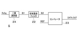
図5は受信器5の第2例を示すブロック図である。図5の受信器5は、二乗演算器24と、低域通過フィルタ22と、コンパレータ23とを有する。二乗演算器24は、絶縁デバイス4を介して受信された変調信号の二乗演算を行う。低域通過フィルタ22は、二乗演算器24の出力信号の振幅を検出する。図5のコンパレータ23の処理動作は図4と同じでる。
FIG. 5 is a block diagram showing a second example of the
図4の絶対値演算器21や図5の二乗演算器24の代わりに、対数や平方根等の非線形な演算を行って振幅情報を検出してもよい。
Instead of the
図6は図4の受信器5内の各部の信号波形図である。図6には、送信器3への入力データDATA_IN、送信器3から出力される変調信号TxSig、受信器5の入力信号RxSig、図4の受信器5内の絶対値演算器21の出力信号B1、低域通過フィルタ22の出力信号B2、及び受信器5の出力データDATA_OUTの各波形が示されている。
FIG. 6 is a signal waveform diagram of each part in the
図6に示すように、送信器3と受信器5は、絶縁デバイス4により電気的に絶縁されているため、送信器3から出力される変調信号TxSigと、受信器5に入力される受信信号RxSigとでは、基準電圧レベルが異なっている。低域通過フィルタ22は、絶対値演算器21の出力信号の振幅を検出した信号B2を出力するが、信号B2にはリップル成分が含まれている。コンパレータ23で基準レベルREFと比較して2値化することで、入力データDATA_INに類似する波形を持つ出力データDATA_OUTが得られる。
As shown in FIG. 6, since the
図7は、図6の入力データDATA_INがハイからローに遷移する時刻の前後の詳細な信号波形図である。図7(a)はパルス発生部12と信号選択部13を設けない場合、図7(b)はパルス発生部12と信号選択部13を設けた場合の信号波形を示している。図7(a)と図7(b)の上段は入力信号がハイからローに遷移するときに発振信号の位相が0度の例を示し、下段は入力信号がハイからローに遷移するときの発振信号の位相が180度の例を示している。
FIG. 7 is a detailed signal waveform diagram before and after the time when the input data DATA_IN of FIG. 6 transitions from high to low. FIG. 7A shows a signal waveform when the
パルス発生部12と信号選択部13を設けない図7(a)の場合、入力データDATA_INがハイからローに遷移する際の発振信号の位相の違いにより、低域通過フィルタ22の出力信号B2にも位相差が生じ、入力データDATA_INがハイからローに遷移する時刻から、復調信号がハイからローに遷移する時刻までの時間差が図7(a)の上段と下段で相違してしまう。この時間差がジッタに相当する。
In the case of FIG. 7A in which the
実際には、入力データDATA_INの立ち下がりにおける発振器11の位相は、入力データDATA_INが発振器11の動作に対して非同期の場合には0~360度の範囲内のランダムな値を取る。
Actually, the phase of the
図7(a)の上段と下段は、それぞれ入力データDATA_INの立ち下がりから復調信号の立ち下がりまでの時間差が最小(=td1)と最大(=td2)になる条件に対応しており、この時間差はtd1~td2の範囲でランダムに分布する。したがって、最大値がtd1~td2の量のランダムなジッタが発生する。 The upper and lower rows of FIG. 7A correspond to the condition that the time difference from the falling edge of the input data DATA_IN to the falling edge of the demodulated signal is the minimum (= td1) and the maximum (= td2), respectively. Is randomly distributed in the range of td1 to td2. Therefore, random jitter with a maximum value of td1 to td2 occurs.
本実施形態に対応した図7(b)では、パルス発生部12が出力するパルス信号の周波数を発振信号の周波数と同一で、かつ1.5周期分のパルス信号を出力する例を示している。入力データDATA_INがハイからローに遷移した直後は、低域通過フィルタ22の出力信号に、入力データDATA_INと発振信号の位相差による波形差が生じているが、入力データDATA_INがハイからローに遷移した直後に、所定の周期分の同一周波数のパルス信号が追加されるため、低域通過フィルタ22の出力信号の波形差は時間とともに小さくなる。
FIG. 7B corresponding to the present embodiment shows an example in which the frequency of the pulse signal output by the
なお、低域通過フィルタ22の出力信号の波形差が顕著な入力データDATA_INの立ち下がり直後においても、低域通過フィルタ22の出力波形と基準レベルREFとの大小関係に変化はないため、出力データDATA_OUTの波形に違いは生じない。
Even immediately after the fall of the input data DATA_IN in which the waveform difference of the output signal of the low
パルス発生部12からのパルス信号の出力が終了すると、低域通過フィルタ22の出力レベルは徐々に低下し、基準レベルREFと交差するタイミングでコンパレータ23の出力論理が反転し、出力データDATA_OUTがローになる。
When the output of the pulse signal from the
以上の動作により、図7(b)に示す本実施形態の例では、入力データDATA_INと発振信号の位相が0度と180度のときで、入力データDATA_INの立ち下がりから、復調信号の立ち下がりまでの時間差td3とtd4はほぼ一致する。これにより、本実施形態によれば、入力データDATA_INの立ち下がり時における、入力データDATA_INと発振信号との位相差のばらつきに起因するジッタを低減できる。 Due to the above operation, in the example of the present embodiment shown in FIG. 7B, when the phases of the input data DATA_IN and the oscillation signal are 0 degrees and 180 degrees, the fall of the input data DATA_IN is followed by the fall of the demodulated signal. The time difference td3 and td4 up to are almost the same. Thereby, according to the present embodiment, it is possible to reduce the jitter caused by the variation in the phase difference between the input data DATA_IN and the oscillation signal at the falling edge of the input data DATA_IN.
本発明者は、本実施形態によるOOK変調器1のジッタ抑圧効果を調べた。具体的には、入力データDATA_INの立ち下がり時の発振信号の位相を10度ステップで変化させ、入力データDATA_INの立ち下がりから受信器5の出力データDATA_OUTの立ち下がりまでの伝搬遅延時間の最大と最小の差を回路シミュレーションにより確認した。これは発振器11の位相が起因で発生しうる最大の伝搬遅延差に相当する。以降、これを最大伝搬遅延差と記述する。最大伝搬遅延差はDATA_INがハイからローに切り替わる際の発振器11の位相が起因で生じるジッタの大きさと強い相関があり、値が小さいほどジッタが少なく、良好な特性といえる。なお、ここでのシミュレーションでは、追加パルスは発振器11と同じ周波数を持つものとしている。
The present inventor investigated the jitter suppressing effect of the
図8は、受信器5の低域通過フィルタ22の次数を2、カットオフ周波数を発振器11の発振周波数と同一とした場合の伝搬遅延特性を示す図である。図8の曲線cb1はパルス発生部12と信号選択部13を設けた本実施形態の場合、曲線cb2はパルス発生部12と信号選択部13を省略した場合の特性を示している。曲線cb1は、曲線cb2に比べて、発振器11の位相が変化しても、伝搬遅延差がより小さいことを示している。これにより、本実施形態では、ジッタ特性が改善していることが確認できた。
FIG. 8 is a diagram showing propagation delay characteristics when the order of the low
図9は、低域通過フィルタ22の次数及びカットオフ周波数、パルス発生部12から出力されるパルス信号のパルス幅を変えた場合の最大伝搬遅延差を示す図である。図9(a)は図4の絶対値演算器21を有する受信器5の最大伝搬遅延差を示し、図9(b)は図5の二乗演算器24を有する受信器5の最大伝搬遅延差を示している。
FIG. 9 is a diagram showing the maximum propagation delay difference when the order and cutoff frequency of the low
図9に示すように、低域通過フィルタ22の次数及びカットオフ周波数、パルス信号のパルス幅、絶対値演算器21又は二乗演算器24を用いた検波方式などを種々変更した場合、最大伝搬遅延差に違いはあるものの、パルス発生部12と信号選択部13を設けて、追加するパルス信号のパルス幅とパルス数を最適化することで、ジッタ特性を改善することができる。
As shown in FIG. 9, when the order and cutoff frequency of the low
このように、第1の実施形態では、OOK変調器1内にパルス発生部12と信号選択部13を設けて、入力データDATA_INがハイからローに遷移するタイミングで、発振器11からの発振信号にパルス信号を付加して変調信号を生成するため、入力データDATA_INと発振信号との位相差がばらついても、受信器5から出力される出力データDATA_OUTの最大伝搬遅延差を小さくでき、ジッタを抑制できる。
As described above, in the first embodiment, the
(第2の実施形態)
第1の実施形態によるOOK変調器1では、入力データDATA_INがハイからローに遷移する際に、発振信号にパルス信号を付加して変調信号を生成するため、付加するパルス信号のパルス幅とパルス数に応じて、変調信号の伝搬遅延時間が増加する。第1の実施形態による変調器1から出力される変調信号の伝搬遅延時間は、入力データDATA_INがハイからローに遷移するときのみ増加し、入力データDATA_INがローからハイに遷移する際には増加しない。このように、入力データDATA_INがローからハイに遷移する場合と、ハイからローに遷移する場合とで、変調信号の伝搬遅延時間に差異が生じる。この結果、入力データDATA_INのパルス幅と、受信器5の出力データDATA_OUTのパルス幅とが相違してしまう。これは、パルス幅歪と呼ばれ、用途によっては好ましくないため、低減するのが望ましい。
(Second embodiment)
In the
図10は第2の実施形態によるOOK変調器1の概略構成を示すブロック図である。図10のOOK変調器1は、図2の構成に加えて、遅延器14を備えている。遅延器14は、入力データDATA_INを所定の時間遅延させて遅延データを出力する。より詳細には、遅延器14は、パルス発生部12が出力するパルス信号の出力期間と略同一時間、入力データDATA_INを遅延させた遅延データを出力する。
FIG. 10 is a block diagram showing a schematic configuration of the
発振器11は、遅延データが第1論理から第2論理に遷移するタイミングに応じて発振を開始し、第2論理から第1論理に遷移するタイミングに応じて発振を停止する。パルス発生部12は、入力データDATA_INが第2論理から第1論理に遷移するタイミングに応じて、予め定めたパルス幅及びパルス数のパルス信号を出力する。信号選択部13は、入力データDATA_INが第2論理のときは発振器11から出力された発振信号を選択し、入力データDATA_INが第1論理のときはパルス発生部12から出力されたパルス信号を選択する。
The
図11は図10のOOK変調器1の動作タイミング図である。時刻t1で入力データDATA_INがローからハイに遷移すると、遅延器14は入力データDATA_INを所定時間遅延させて遅延データを出力する。これにより、遅延データは時刻t2でローからハイに遷移する。
FIG. 11 is an operation timing diagram of the
発振器11は、遅延データがローからハイに遷移すると、発振動作を開始して、発振信号を出力する。その後、時刻t3で入力データDATA_INがハイからローに遷移すると、パルス発生部12は、パルス信号の出力を開始する。この時点では、発振器11はまだ発振動作を継続しているが、信号選択部13は、時刻t3で発振信号の選択からパルス信号の選択に切り替える。その後、時刻t4になると、発振器11は発振動作を停止する。パルス発生部12は、時刻t3から、予め定めたパルス幅及びパルス数のパルス信号を出力する。
When the delay data transitions from low to high, the
このように、第2の実施形態では、発振器11の前段に遅延器14を接続して入力データDATA_INを遅延させるため、入力データDATA_INがハイからローに遷移するときだけでなく、ローからハイに遷移するときも、変調信号を遅延させることができ、入力データDATA_INのパルス幅と、受信器5の出力データDATA_OUTのパルス幅とを略一致させることができ、パルス幅歪みを抑制できる。
As described above, in the second embodiment, since the
(第3の実施形態)
第1及び第2の実施形態における発振器11は、遅延回路付きのリング発振回路で構成可能である。
(Third embodiment)
The
図12は第3の実施形態によるOOK変調器1の概略構成を示すブロック図である。図12のOOK変調器1は、発振器11と、パルス発生部12と、信号選択部13を備えている点では図2や図10のOOK変調器1と一致するが、発振器11の内部構成が図2や図10の発振器11とは異なる。図12の発振器11は、入力データDATA_INを順繰りに遅延させる複数段の遅延回路15と、複数段の遅延回路15のうち最終段の遅延回路15の出力データを反転遅延させて最終段の遅延回路15の入力側に帰還させて発振信号を生成するリング発振回路16とを有する。
FIG. 12 is a block diagram showing a schematic configuration of the
パルス発生部12は、複数段の遅延回路15の各段の出力データに基づいてパルス信号を生成する。複数段の遅延回路15での遅延時間をパルス発生部12が出力するパルス信号の出力期間に合わせることで、複数段の遅延回路15を図10の遅延器14として利用することができる。
The
図13は図12に対応するOOK変調器1の具体的な回路図である。図13における複数段の遅延回路15は、直列接続された3つのインバータ31~33で構成されている。そのうちの最終段のインバータ33の後段には、入力データDATA_INと論理を合わせるために、別個のインバータ34が接続されている。複数段の遅延回路15を構成するインバータ31~33の接続段数は任意である。また、インバータ以外の、反転論理の信号を出力する論理ゲートを用いて複数段の遅延回路15を構成してもよい。
FIG. 13 is a specific circuit diagram of the
図13のリング発振回路16は、ANDゲート35と、インバータ36とで構成されている。ANDゲート35の後段にインバータ36が接続され、インバータ36の出力は帰還されて、ANDゲート35に入力される。ANDゲート35は、インバータ34の出力と、インバータ36の出力との論理積を演算する。リング発振回路16の後段には、入力データDATA_INと論理を合わせるために、別個のインバータ37が接続されており、このインバータ37から発振信号が出力される。図13のリング発振回路16は、奇数段の論理反転素子をリング状に接続すれば構成でき、論理反転素子の種類と接続段数は任意である。
The
図13のパルス発生部12は、入力データDATA_INと1段目のインバータ31の出力との排他的論理和を演算するXORゲート38と、2段目のインバータ32の出力と3段目のインバータ33の出力との排他的論理和を演算するXORゲート39と、これらXORゲート38,39の出力の論理積を演算するANDゲート40と、ANDゲート40の出力を反転するインバータ41とを有する。
The
図14は図13のOOK変調器1の動作タイミング図である。インバータ31、インバータ32、インバータ33、インバータ36は他の論理回路ブロックに比べて有意な遅延を有する遅延回路として構成されているものとして説明する。時刻t1で入力データDATA_INがローからハイに遷移すると、複数段の遅延回路15内の1段目のインバータ31の出力は時刻t2でハイからローに遷移する。このとき、XORゲート38は、時刻t1でハイからローに遷移し、時刻t2でローからハイに遷移する。これにより、パルス発生部12は、時刻t1~t2の間に、最初のパルスを出力する。
FIG. 14 is an operation timing diagram of the
その後、時刻t3で、2段目のインバータ32の出力はローからハイに遷移する。その後、時刻t4で、3段目のインバータ33の出力はハイからローに遷移する。XORゲート39は、時刻t3でハイからローに遷移し、時刻t4でローからハイに遷移する。これにより、パルス発生部12は、時刻t3~t4の間に、2つ目のパルスを出力する。
After that, at time t3, the output of the
時刻t4で、リング発振回路16の入力がハイになって、リング発振回路16は発振動作を開始し、発振信号を出力する。信号選択部13は、入力データDATA_INがハイの間はリング発振回路16から出力された発振信号を選択するため、時刻t4以降に発振信号が変調信号として出力される。
At time t4, the input of the
その後、時刻t5で、入力データDATA_INがハイからローに遷移すると、信号選択部13は、パルス発生部12から出力されたパルス信号を選択する。
After that, when the input data DATA_IN transitions from high to low at time t5, the
時刻t5で、入力データDATA_INがハイからローに遷移すると、複数段の遅延回路15内の1段目のインバータ31の出力は時刻t6でローからハイに遷移する。XORゲート38の出力は、時刻t5でハイからローに遷移し、時刻t6でローからハイに遷移する。また、XORゲート38は、時刻t5~t6の間、ローになる。よって、パルス発生部12は、時刻t5~t6の間、入力データDATA_INがハイからローに遷移した後では最初のパルスを出力する。
When the input data DATA_IN transitions from high to low at time t5, the output of the
その後、時刻t7で2段目のインバータ32の出力はハイからローに遷移し、時刻t8で3段目のインバータ33の出力はローからハイに遷移する。よって、パルス発生部12は、時刻t7~t8の間、入力データDATA_INがハイからローに遷移した後では2つ目のパルスを出力する。
After that, at time t7, the output of the second-
時刻t5以降は、信号選択部13は、パルス発生部12から出力されたパルス信号を選択する。よって、入力データDATA_INがハイからローに遷移すると、発振器11から出力された発振信号に、所定のパルス幅かつパルス数のパルス信号が付加された変調信号が出力される。
After the time t5, the
このように、第3の実施形態によるOOK変調器1では、複数段の遅延回路15とリング発振回路16にて発振器11を構成するため、入力データDATA_INがハイからローに遷移した直後に出力されるパルス信号の出力期間に合わせて複数段の遅延回路15の遅延時間を設定することで、第2の実施形態と同様に、入力データDATA_INのパルス期間と、受信器5の出力データDATA_OUTのパルス期間とを略一致させることができる。また、複数段の遅延回路15を構成する各段の遅延回路15の出力を用いることで、パルス発生部12から出力されるパルス信号を生成できる。これにより、パルス発生部12の構成を簡略化できる。
As described above, in the
(第4の実施形態)
上述した第2の実施形態では、入力データDATA_INがハイからローに遷移する際の変調信号の遅延時間を抑制するために、発振器11の前段に遅延器14を接続する例を説明した。これに対して、第4の実施形態は、発振器11の前段に遅延器14を接続する代わりに、受信器5側にタイミング調整部を設けるものである。
(Fourth Embodiment)
In the second embodiment described above, an example in which the
図15は第4の実施形態による信号伝送システム2の概略構成を示すブロック図である。図15の信号伝送システム2は、図1と同様の構成に加えて、受信器5内の復調器7の後段側にタイミング調整部8を備えている。
FIG. 15 is a block diagram showing a schematic configuration of the
タイミング調整部8は、OOK変調器1内のパルス発生部12から出力されたパルス信号のパルス幅及びパルス数に基づいて、復調器7の出力データDATA_OUTの先頭部分のタイミングを調整する。すなわち、タイミング調整部8は、入力データDATA_INがローからハイに遷移するタイミングに対応づけて、復調器7の出力データDATA_OUTがローからハイに遷移するタイミングを調整する。より具体的には、タイミング調整部8は、入力データDATA_INがハイからローに遷移した直後にパルス発生部12が出力するパルス信号の出力期間に合わせて、復調器7の出力データDATA_OUTがローからハイに遷移するタイミングを調整する。
The
タイミング調整部8は、復調器7の出力データDATA_OUTを遅延させる遅延回路15等を用いて構成可能である。タイミング調整部8が復調器7の出力データDATA_OUTを遅延させる遅延時間は、製造時のテスト等で決定してもよいし、遅延回路15を構成する配線パターンのトリミング等により遅延時間を調整してもよい。また、起動時や所定時間ごとに、既知のパルス幅の入力データDATA_INをOOK変調器1に入力して、タイミング調整部8の遅延時間を再調整してもよい。
The
また、図10の遅延器14と図15のタイミング調整部8を両方備えた信号伝送システム2を構築してもよい。
Further, the
このように、第4の実施形態では、入力データDATA_INがハイからローに遷移する際に変調信号にパルス信号が付加されるため、変調信号に遅延が生じることに伴って、受信器5内の復調器7の後段にタイミング調整部8を設けて、出力データDATA_OUTがローからハイに遷移するタイミングを調整する。これにより、第2の実施形態と同様に、入力データDATA_INのパルス幅と受信器5の出力データDATA_OUTのパルス幅とを略一致させることができる。
As described above, in the fourth embodiment, the pulse signal is added to the modulated signal when the input data DATA_IN transitions from high to low, so that the modulated signal is delayed and the
(第5の実施形態)
上述した第1~第4の実施形態におけるパルス発生部12から出力されるパルス信号は、入力データDATA_INの立ち下がりごとに変動しないパルス波形を持っていればよく、パルス信号の周波数は必ずしも発振器11から出力される発振信号の周波数と同一でなくてもよい。このため、発振器11は、LC発振回路やリング発振回路16など、任意の回路方式の発振回路でよい。また、パルス発生部12も任意の回路構成にて構成可能である。ただし、発振器11から出力される発振信号の周波数とパルス発生部12から出力されるパルス信号の周波数が著しくかけ離れていると、絶縁デバイス4や受信器5の通過信号帯域を広くしなければならず、システム構成が複雑化し、コストも嵩んでしまう。このような観点から、パルス発生部12から出力されるパルス信号の周波数は、発振器11から出力される発振信号の周波数と概ね一致させるのが望ましい。
(Fifth Embodiment)
The pulse signal output from the
(第6の実施形態)
第6の実施形態によるOOK変調器1は、第1~第5の実施形態とは根本的に異なる構成を備えている。
(Sixth Embodiment)
The
図16は第6の実施形態によるOOK変調器1の回路図である。図16のOOK変調器1は、第1発振器11aと、第1計測器17と、第2発振器11bと、第2計測器18と、発振制御部19と、信号選択部13とを備えている。
FIG. 16 is a circuit diagram of the
第1発振器11aは、入力データDATA_INが第1論理から第2論理に遷移するタイミングに応じて発振を開始し、第2論理から第1論理に遷移するタイミングに応じて発振を停止する。第1発振器11aは、リング発振回路16で構成可能である。第1発振器11aを構成するリング発振回路16は、ANDゲート51と、インバータ52とを有する。ANDゲート51の出力はインバータ52に入力され、インバータ52の出力と入力データDATA_INはANDゲート51に入力される。インバータ52の出力は、別のインバータ53にて論理が反転されて、発振信号が生成される。
The
第1計測器17は、第1発振器11aの発振回数が第1発振回数に到達したことを検知する。第1計測器17は、縦続接続された2つのフリップフロップ54,55を有する。各フリップフロップ54,55は、第1発振器11aから出力された発振信号に同期して動作する。各フリップフロップ54,55は、発振制御部19の出力信号がハイのときにリセット状態になる。2段目のフリップフロップ55の出力は、信号選択部13の選択信号として用いられる。
The
第2発振器11bは、入力データDATA_INが第2論理から第1論理に遷移するタイミングに応じて発振を開始する。第2発振器11bは、例えばリング発振回路16で構成可能である。第2発振器11bを構成するリング発振回路16は、ANDゲート56と、インバータ57とを有する。ANDゲート56の出力はインバータ57に入力され、インバータ57の出力と発振制御部19の出力はANDゲート56に入力される。インバータ57の出力は、別のインバータ58にて論理が反転されて、パルス信号が生成される。
The second oscillator 11b starts oscillation according to the timing at which the input data DATA_IN transitions from the second logic to the first logic. The second oscillator 11b can be configured by, for example, a
第2計測器18は、第2発振器11bの発振回数が第2発振回数に到達したことを検知する。第2計測器18は、縦続接続された2つのフリップフロップ59,60を有する。各フリップフロップ59,60は、第2発振器11bから出力された発振信号に同期して動作する。各フリップフロップ59,60は、入力データDATA_INがハイのときにリセット状態になる。2段目のフリップフロップ60の出力は、発振制御部19に入力される。
The
発振制御部19は、第2計測器18で第2発振回数に到達したことが検知されると、第2発振器11bの発振動作を停止させる。発振制御部19は、インバータ61と、ANDゲート62と、インバータ63とを有する。インバータ61は、入力データDATA_INを反転出力する。インバータ63は、第2計測器18内の2段目のフリップフロップ60の出力を反転出力する。ANDゲート62は、インバータ61の出力と、インバータ63の出力との論理積信号を出力する。ANDゲート62の出力は、第1計測器17内の2つのフリップフロップ54,55のリセット端子に入力されるとともに、第2発振器11b内のANDゲート56に入力される。
When the
信号選択部13は、第1計測器17で第1発振回数に到達したことが検知されてから、入力データDATA_INが第2論理から第1論理に遷移するまでは第1発振器11aから出力された発振信号を選択し、入力データDATA_INが第2論理から第1論理に遷移した以降は第2発振器11bから出力された発振信号を選択する。
The
図17は第16のOOK変調器1の動作タイミング図である。時刻t1で入力データDATA_INがローからハイに遷移すると、第1発振器11aは発振動作を開始し、発振信号を出力する。また、時刻t1で入力データDATA_INがハイになると、第2計測器18内の2つのフリップフロップ59,60はリセット状態になり、2段目のフリップフロップ60はローを出力し、インバータ63の出力はハイになる。
FIG. 17 is an operation timing diagram of the 16th
また、時刻t1で、発振制御部19内のインバータ61の出力はローになり、ANDゲート62の出力はローになる。これにより、第1計測器17内の2つのフリップフロップ54,55のリセット状態は解除される。その後、これらフリップフロップ54,55は、第1発振器11aから出力される発振信号の数を計測する。
Further, at time t1, the output of the
時刻t2になると、第1計測器17内の2段目のフリップフロップ55の出力E1はローからハイに遷移する。これにより、信号選択部13は、第1発振器11aから出力された発振信号を変調信号として選択する。
At time t2, the output E1 of the second stage flip-
その後、時刻t3で、入力データDATA_INがハイからローに遷移すると、発振制御部19内のANDゲート62の出力E5はハイに遷移する。これにより、第2発振器11bは発振動作を開始する。また、ANDゲート62の出力E5がハイになると、第1計測器17内の2つのフリップフロップ54,55はリセット状態になる。よって、2段目のフリップフロップ55の出力E1はローになる。これにより、信号選択部13は、第2発振器11bから出力された発振信号を変調信号として選択する。その後、時刻t4になると、第2計測器18内の2段目のフリップフロップ59の出力がハイになるため、発振制御部19内のANDゲート62の出力E5がローになり、第2発振器11bは発振動作を停止する。
After that, when the input data DATA_IN transitions from high to low at time t3, the output E5 of the AND
このように、第6の実施形態によるOOK変調器1では、入力データDATA_INがローからハイに遷移すると、第1発振器11aから出力される発振信号の発振回数が所定回数に到達するまで第1計測器17で計測し、所定回数に到達すると、発振信号を信号選択部13にて選択する。その後、入力データDATA_INがハイからローに遷移すると、第2発振器11bでの発振動作を開始させて発振信号を出力するとともに、この発振信号を信号選択部13が選択するようにする。これにより、変調信号が出力される期間を入力データDATA_INのパルス幅に合わせることができる。
As described above, in the
また、入力データDATA_INがハイからローに遷移する際に、変調信号に付加されるパルス数は、第2計測器18内のフリップフロップ59,60の段数によって調整できる。
Further, the number of pulses added to the modulation signal when the input data DATA_IN transitions from high to low can be adjusted by the number of stages of the flip-
本発明のいくつかの実施形態を説明したが、これらの実施形態は、例として提示したものであり、発明の範囲を限定することは意図していない。これら新規な実施形態は、その他の様々な形態で実施されることが可能であり、発明の要旨を逸脱しない範囲で、種々の省略、置き換え、変更を行うことができる。これら実施形態やその変形は、発明の範囲や要旨に含まれるとともに、特許請求の範囲に記載された発明とその均等の範囲に含まれる。 Although some embodiments of the present invention have been described, these embodiments are presented as examples and are not intended to limit the scope of the invention. These novel embodiments can be implemented in various other embodiments, and various omissions, replacements, and changes can be made without departing from the gist of the invention. These embodiments and variations thereof are included in the scope and gist of the invention, and are also included in the scope of the invention described in the claims and the equivalent scope thereof.
1 OOK変調器、2 信号伝送システム、3 送信器、4 絶縁デバイス、5 受信器、6 ドライバ、7 復調器、8 タイミング調整部、11 発振器、11a 第1発振器、11b 第2発振器、12 パルス発生部、13 信号選択部、14 遅延器、15 遅延回路、16 リング発振回路、17 第1計測器、18 第2計測器、19 発振制御部、21 絶対値演算器、22 低域通過フィルタ、23 コンパレータ、24 二乗演算器 1 OK modulator, 2 signal transmission system, 3 transmitter, 4 isolated device, 5 receiver, 6 driver, 7 demodulator, 8 timing adjuster, 11 oscillator, 11a first oscillator, 11b second oscillator, 12 pulse generation Unit, 13 Signal selection unit, 14 Delayer, 15 Delay circuit, 16 Ring oscillation circuit, 17 1st instrument, 18 2nd instrument, 19 Oscillation control unit, 21 Absolute value calculator, 22 Low frequency pass filter, 23 Oscillator, 24 squared calculator
Claims (8)
前記入力データが前記第2論理から前記第1論理に遷移するタイミングに応じて、予め定めたパルス幅及びパルス数のパルス信号を出力するパルス発生部と、
前記入力データが前記第2論理のときは前記発振器から出力された発振信号を選択し、前記入力データが前記第1論理のときは前記パルス発生部から出力された前記パルス信号を選択する信号選択部と、を備える、変調器。 An oscillator that starts oscillation according to the timing when the input data transitions from the first logic to the second logic, and stops oscillation according to the timing when the input data transitions from the second logic to the first logic.
A pulse generation unit that outputs a pulse signal having a predetermined pulse width and number of pulses according to the timing at which the input data transitions from the second logic to the first logic.
When the input data is the second logic, the oscillation signal output from the oscillator is selected, and when the input data is the first logic, the pulse signal output from the pulse generator is selected. A modulator, including a unit.
前記遅延データが第1論理から第2論理に遷移するタイミングに応じて発振を開始し、前記第2論理から前記第1論理に遷移するタイミングに応じて発振を停止する発振器と、
前記入力データが前記第2論理から前記第1論理に遷移するタイミングに応じて、予め定めたパルス幅及びパルス数のパルス信号を出力するパルス発生部と、
前記入力データが前記第2論理のときは前記発振器から出力された発振信号を選択し、前記入力データが前記第1論理のときは前記パルス発生部から出力された前記パルス信号を選択する信号選択部と、を備える、変調器。 A delay device that outputs delayed data with the input data delayed for a predetermined time,
An oscillator that starts oscillation according to the timing at which the delay data transitions from the first logic to the second logic, and stops oscillation at the timing when the delay data transitions from the second logic to the first logic.
A pulse generation unit that outputs a pulse signal having a predetermined pulse width and number of pulses according to the timing at which the input data transitions from the second logic to the first logic.
When the input data is the second logic, the oscillation signal output from the oscillator is selected, and when the input data is the first logic, the pulse signal output from the pulse generator is selected. A modulator, including a unit.
前記入力データを遅延させる第1遅延回路と、
前記遅延された入力データをさらに遅延させる第2遅延回路と、
前記第2遅延回路の出力データ及び前記第2遅延回路の出力データを反転遅延させたデータに基づいて発振信号を生成する発振回路と、を有する、請求項1に記載の変調器。 The oscillator is
The first delay circuit that delays the input data and
A second delay circuit that further delays the delayed input data,
The modulator according to claim 1, further comprising an oscillation circuit that generates an oscillation signal based on the output data of the second delay circuit and the data obtained by inverting and delaying the output data of the second delay circuit .
前記遅延された入力データをさらに遅延させる第2遅延回路と、A second delay circuit that further delays the delayed input data,
前記さらに遅延された入力データが第1論理から第2論理に遷移するタイミングに応じて発振を開始し、前記第2遅延回路の出力データ及び前記第2遅延回路の出力データを反転遅延させたデータに基づいて発振信号を生成する発振回路と、Oscillation is started according to the timing at which the further delayed input data transitions from the first logic to the second logic, and the output data of the second delay circuit and the output data of the second delay circuit are inverted and delayed. An oscillator circuit that generates an oscillation signal based on
前記入力データが前記第1論理から前記第2論理に遷移するタイミングに応じて、予め定めたパルス幅及びパルス数のパルス信号を出力するパルス発生部と、A pulse generation unit that outputs a pulse signal having a predetermined pulse width and number of pulses according to the timing at which the input data transitions from the first logic to the second logic.
前記入力データが前記第1論理のときは前記発振回路から出力された発振信号を選択し、前記入力データが前記第2論理のときは前記パルス発生部から出力された前記パルス信号を選択する信号選択部と、を備える、変調器。When the input data is the first logic, the oscillation signal output from the oscillation circuit is selected, and when the input data is the second logic, the pulse signal output from the pulse generator is selected. A modulator, including a selection unit.
前記第2遅延回路は、前記パルス信号のパルス幅で前記遅延された入力データをさらに遅延させ、
前記パルス発生部は、前記入力データ、前記遅延された入力データ、及び前記さらに遅延された入力データに基づいて前記パルス信号を生成する、請求項3又は4に記載の変調器。 The first delay circuit delays the input data by the pulse width of the pulse signal.
The second delay circuit further delays the delayed input data by the pulse width of the pulse signal.
The modulator according to claim 3 or 4, wherein the pulse generator generates the pulse signal based on the input data, the delayed input data, and the further delayed input data .
前記第1発振器の発振回数が第1発振回数に到達したことを検知する第1計測器と、
前記入力データが前記第2論理から前記第1論理に遷移するタイミングに応じて発振を開始する第2発振器と、
前記第2発振器の発振回数が第2発振回数に到達したことを検知する第2計測器と、
前記第2計測器で前記第2発振回数に到達したことが検知されると、前記第2発振器の発振動作を停止させる発振制御部と、
前記第1計測器で前記第1発振回数に到達したことが検知されてから、前記入力データが前記第2論理から前記第1論理に遷移するまでは前記第1発振器から出力された発振信号を選択し、前記入力データが前記第2論理から前記第1論理に遷移した以降は前記第2発振器から出力された発振信号を選択する信号選択部と、を備える、変調器。 A first oscillator that starts oscillation according to the timing when the input data transitions from the first logic to the second logic, and stops oscillation according to the timing when the input data transitions from the second logic to the first logic.
A first measuring instrument that detects that the number of oscillations of the first oscillator has reached the first number of oscillations,
A second oscillator that starts oscillation according to the timing at which the input data transitions from the second logic to the first logic.
A second measuring instrument that detects that the number of oscillations of the second oscillator has reached the number of second oscillations,
When the second measuring instrument detects that the second oscillation number has been reached, the oscillation control unit that stops the oscillation operation of the second oscillator and the oscillation control unit.
The oscillation signal output from the first oscillator is used until the input data transitions from the second logic to the first logic after the first measuring instrument detects that the first oscillation count has been reached. A modulator comprising a signal selection unit for selecting and selecting an oscillation signal output from the second oscillator after the input data has transitioned from the second logic to the first logic.
前記送信器から出力された変調信号を絶縁した状態で伝送する絶縁デバイスと、
前記絶縁デバイスを介して伝送された前記変調信号を復調する復調器を有する受信器と、を備える、信号伝送システム。 A transmitter having the modulator according to any one of claims 1 to 6.
An isolated device that transmits the modulated signal output from the transmitter in an isolated state, and
A signal transmission system comprising a receiver having a demodulator that demodulates the modulated signal transmitted via the isolated device.
前記送信器から出力された変調信号を絶縁した状態で伝送する絶縁デバイスと、An isolated device that transmits the modulated signal output from the transmitter in an isolated state, and
前記絶縁デバイスを介して伝送された前記変調信号を復調する復調器を有する受信器と、を備え、A receiver having a demodulator that demodulates the modulated signal transmitted via the isolated device.
前記変調器は、 The modulator is
入力データが第1論理から第2論理に遷移するタイミングに応じて発振を開始し、前記第2論理から前記第1論理に遷移するタイミングに応じて発振を停止する発振器と、An oscillator that starts oscillation according to the timing when the input data transitions from the first logic to the second logic, and stops oscillation according to the timing when the input data transitions from the second logic to the first logic.
前記入力データが前記第2論理から前記第1論理に遷移するタイミングに応じて、予め定めたパルス幅及びパルス数のパルス信号を出力するパルス発生部と、A pulse generation unit that outputs a pulse signal having a predetermined pulse width and number of pulses according to the timing at which the input data transitions from the second logic to the first logic.
前記入力データが前記第2論理のときは前記発振器から出力された発振信号を選択し、前記入力データが前記第1論理のときは前記パルス発生部から出力された前記パルス信号を選択する信号選択部と、を有し、When the input data is the second logic, the oscillation signal output from the oscillator is selected, and when the input data is the first logic, the pulse signal output from the pulse generator is selected. With a part,
前記受信器は、前記パルス信号のパルス幅及びパルス数に基づいて、前記復調された変調信号が出力されるタイミングを調整するタイミング調整部を有する、信号伝送システム。The receiver is a signal transmission system having a timing adjusting unit that adjusts the timing at which the demodulated modulated signal is output based on the pulse width and the number of pulses of the pulse signal.
Priority Applications (2)
| Application Number | Priority Date | Filing Date | Title |
|---|---|---|---|
| JP2018168233A JP7021033B2 (en) | 2018-09-07 | 2018-09-07 | Modulator and signal transmission system |
| US16/290,098 US10666474B2 (en) | 2018-09-07 | 2019-03-01 | Modulator and signal transmission system |
Applications Claiming Priority (1)
| Application Number | Priority Date | Filing Date | Title |
|---|---|---|---|
| JP2018168233A JP7021033B2 (en) | 2018-09-07 | 2018-09-07 | Modulator and signal transmission system |
Publications (2)
| Publication Number | Publication Date |
|---|---|
| JP2020043429A JP2020043429A (en) | 2020-03-19 |
| JP7021033B2 true JP7021033B2 (en) | 2022-02-16 |
Family
ID=69720156
Family Applications (1)
| Application Number | Title | Priority Date | Filing Date |
|---|---|---|---|
| JP2018168233A Active JP7021033B2 (en) | 2018-09-07 | 2018-09-07 | Modulator and signal transmission system |
Country Status (2)
| Country | Link |
|---|---|
| US (1) | US10666474B2 (en) |
| JP (1) | JP7021033B2 (en) |
Families Citing this family (1)
| Publication number | Priority date | Publication date | Assignee | Title |
|---|---|---|---|---|
| JP7366849B2 (en) * | 2020-07-09 | 2023-10-23 | 株式会社東芝 | Communication device |
Citations (3)
| Publication number | Priority date | Publication date | Assignee | Title |
|---|---|---|---|---|
| JP2001177584A (en) | 1999-12-17 | 2001-06-29 | Tamura Electric Works Ltd | Modulator circuit |
| JP2002043067A (en) | 2000-07-21 | 2002-02-08 | Matsushita Electric Works Ltd | Lighting equipment |
| US20150171901A1 (en) | 2013-12-13 | 2015-06-18 | Silicon Laboratories Inc. | Techniques for reduced jitter in digital isolators |
Family Cites Families (10)
| Publication number | Priority date | Publication date | Assignee | Title |
|---|---|---|---|---|
| US4415861A (en) * | 1981-06-08 | 1983-11-15 | Tektronix, Inc. | Programmable pulse generator |
| JPS63268336A (en) * | 1987-04-24 | 1988-11-07 | Matsushita Electric Works Ltd | Pulse modulation transmission circuit |
| JP2825252B2 (en) * | 1989-01-20 | 1998-11-18 | 株式会社東芝 | Waveform shaping circuit |
| JPH0615308Y2 (en) * | 1989-06-08 | 1994-04-20 | 株式会社ケンウッド | Keying circuit |
| JP3077154B2 (en) * | 1990-03-02 | 2000-08-14 | ソニー株式会社 | Enhancer circuit |
| JP2900772B2 (en) * | 1993-12-24 | 1999-06-02 | 株式会社デンソー | Composite device of pulse phase difference encoding circuit and pulse generation circuit and digital control PLL device |
| JP4282998B2 (en) * | 2003-01-08 | 2009-06-24 | パナソニック株式会社 | Modulator and correction method thereof |
| US7459951B2 (en) * | 2006-02-22 | 2008-12-02 | Exar Corporation | Self-calibrating digital pulse-width modulator (DPWM) |
| JP4106383B2 (en) * | 2006-06-08 | 2008-06-25 | インターナショナル・ビジネス・マシーンズ・コーポレーション | Delay ratio adjustment circuit, delay pulse generation circuit, and pulse width modulation pulse signal generator. |
| US9154145B2 (en) * | 2011-05-02 | 2015-10-06 | Rambus Inc. | Integrated circuit having a multiplying injection-locked oscillator |
-
2018
- 2018-09-07 JP JP2018168233A patent/JP7021033B2/en active Active
-
2019
- 2019-03-01 US US16/290,098 patent/US10666474B2/en active Active
Patent Citations (3)
| Publication number | Priority date | Publication date | Assignee | Title |
|---|---|---|---|---|
| JP2001177584A (en) | 1999-12-17 | 2001-06-29 | Tamura Electric Works Ltd | Modulator circuit |
| JP2002043067A (en) | 2000-07-21 | 2002-02-08 | Matsushita Electric Works Ltd | Lighting equipment |
| US20150171901A1 (en) | 2013-12-13 | 2015-06-18 | Silicon Laboratories Inc. | Techniques for reduced jitter in digital isolators |
Also Published As
| Publication number | Publication date |
|---|---|
| US10666474B2 (en) | 2020-05-26 |
| US20200084075A1 (en) | 2020-03-12 |
| JP2020043429A (en) | 2020-03-19 |
Similar Documents
| Publication | Publication Date | Title |
|---|---|---|
| KR100459709B1 (en) | Serializer-deserializer circuit having enough set up and hold time margin | |
| US8634509B2 (en) | Synchronized clock phase interpolator | |
| US7667544B2 (en) | Clock reproducing apparatus | |
| US6819153B2 (en) | Semiconductor device for clock signals synchronization accuracy | |
| KR101326117B1 (en) | A digital delay-locked loop using a phase-inversion algorithm and method for controlling the same | |
| WO2012147258A1 (en) | Inter-channel skew adjustment circuit | |
| WO2014041924A1 (en) | Clock-generating device and clock data recovery device | |
| KR20170112674A (en) | Device for correcting multi-phase clock signal | |
| US8804887B2 (en) | Transmission and receiving apparatus and method having different sending and receiving clocks | |
| JP7021033B2 (en) | Modulator and signal transmission system | |
| JP5491454B2 (en) | Parallel-serial conversion circuit | |
| JP4992947B2 (en) | Parallel-serial converter and parallel data output device | |
| TWI578708B (en) | Interpolator systems and methods | |
| US20150102862A1 (en) | Oscillator | |
| US9762228B2 (en) | High-speed programmable clock divider | |
| JP5697066B1 (en) | Pulse generator | |
| TW201417508A (en) | Ring oscillator | |
| JP3476448B2 (en) | Signal synchronization circuit | |
| US9762183B2 (en) | Voltage-controlled ring oscillator with delay line | |
| JP6823268B2 (en) | Frequency divider circuit, demultiplexer circuit, and semiconductor integrated circuit | |
| US20100141319A1 (en) | Clock signal output circuit | |
| JP5038323B2 (en) | Jitter injection apparatus, jitter injection method, test apparatus, and communication chip | |
| CN115441865A (en) | Phase interpolator and phase interpolation method of clock signal | |
| US10326456B2 (en) | Phase combiner circuit | |
| JP2002094495A (en) | Voltage-controlled oscillator and multi-bit rate timing extracting circuit using the same |
Legal Events
| Date | Code | Title | Description |
|---|---|---|---|
| A621 | Written request for application examination |
Free format text: JAPANESE INTERMEDIATE CODE: A621 Effective date: 20200625 |
|
| A977 | Report on retrieval |
Free format text: JAPANESE INTERMEDIATE CODE: A971007 Effective date: 20210622 |
|
| A131 | Notification of reasons for refusal |
Free format text: JAPANESE INTERMEDIATE CODE: A131 Effective date: 20210831 |
|
| A521 | Request for written amendment filed |
Free format text: JAPANESE INTERMEDIATE CODE: A523 Effective date: 20211101 |
|
| TRDD | Decision of grant or rejection written | ||
| A01 | Written decision to grant a patent or to grant a registration (utility model) |
Free format text: JAPANESE INTERMEDIATE CODE: A01 Effective date: 20220104 |
|
| A61 | First payment of annual fees (during grant procedure) |
Free format text: JAPANESE INTERMEDIATE CODE: A61 Effective date: 20220203 |
|
| R151 | Written notification of patent or utility model registration |
Ref document number: 7021033 Country of ref document: JP Free format text: JAPANESE INTERMEDIATE CODE: R151 |