JP6984800B1 - Elastic wave device - Google Patents
Elastic wave device Download PDFInfo
- Publication number
- JP6984800B1 JP6984800B1 JP2021541525A JP2021541525A JP6984800B1 JP 6984800 B1 JP6984800 B1 JP 6984800B1 JP 2021541525 A JP2021541525 A JP 2021541525A JP 2021541525 A JP2021541525 A JP 2021541525A JP 6984800 B1 JP6984800 B1 JP 6984800B1
- Authority
- JP
- Japan
- Prior art keywords
- electrode
- piezoelectric film
- elastic wave
- wave device
- support member
- Prior art date
- Legal status (The legal status is an assumption and is not a legal conclusion. Google has not performed a legal analysis and makes no representation as to the accuracy of the status listed.)
- Active
Links
- 239000000758 substrate Substances 0.000 claims abstract description 62
- 229910052751 metal Inorganic materials 0.000 claims description 21
- 239000002184 metal Substances 0.000 claims description 21
- 239000000463 material Substances 0.000 claims description 16
- WSMQKESQZFQMFW-UHFFFAOYSA-N 5-methyl-pyrazole-3-carboxylic acid Chemical compound CC1=CC(C(O)=O)=NN1 WSMQKESQZFQMFW-UHFFFAOYSA-N 0.000 claims description 6
- GQYHUHYESMUTHG-UHFFFAOYSA-N lithium niobate Chemical compound [Li+].[O-][Nb](=O)=O GQYHUHYESMUTHG-UHFFFAOYSA-N 0.000 claims description 6
- PMHQVHHXPFUNSP-UHFFFAOYSA-M copper(1+);methylsulfanylmethane;bromide Chemical compound Br[Cu].CSC PMHQVHHXPFUNSP-UHFFFAOYSA-M 0.000 claims description 3
- 238000012986 modification Methods 0.000 description 29
- 230000004048 modification Effects 0.000 description 29
- 230000005284 excitation Effects 0.000 description 23
- 239000010410 layer Substances 0.000 description 15
- 238000006073 displacement reaction Methods 0.000 description 12
- 238000000034 method Methods 0.000 description 8
- 230000000052 comparative effect Effects 0.000 description 7
- 235000019687 Lamb Nutrition 0.000 description 5
- 230000002542 deteriorative effect Effects 0.000 description 5
- 229910013641 LiNbO 3 Inorganic materials 0.000 description 4
- XUIMIQQOPSSXEZ-UHFFFAOYSA-N Silicon Chemical compound [Si] XUIMIQQOPSSXEZ-UHFFFAOYSA-N 0.000 description 4
- 238000010586 diagram Methods 0.000 description 4
- 230000001902 propagating effect Effects 0.000 description 4
- 239000010703 silicon Substances 0.000 description 4
- 229910052581 Si3N4 Inorganic materials 0.000 description 3
- 229910045601 alloy Inorganic materials 0.000 description 3
- 239000000956 alloy Substances 0.000 description 3
- 238000013461 design Methods 0.000 description 3
- 230000017525 heat dissipation Effects 0.000 description 3
- 229910052710 silicon Inorganic materials 0.000 description 3
- 229910016570 AlCu Inorganic materials 0.000 description 2
- CPLXHLVBOLITMK-UHFFFAOYSA-N Magnesium oxide Chemical compound [Mg]=O CPLXHLVBOLITMK-UHFFFAOYSA-N 0.000 description 2
- MCMNRKCIXSYSNV-UHFFFAOYSA-N Zirconium dioxide Chemical compound O=[Zr]=O MCMNRKCIXSYSNV-UHFFFAOYSA-N 0.000 description 2
- PNEYBMLMFCGWSK-UHFFFAOYSA-N aluminium oxide Inorganic materials [O-2].[O-2].[O-2].[Al+3].[Al+3] PNEYBMLMFCGWSK-UHFFFAOYSA-N 0.000 description 2
- 230000008878 coupling Effects 0.000 description 2
- 238000010168 coupling process Methods 0.000 description 2
- 238000005859 coupling reaction Methods 0.000 description 2
- 239000004065 semiconductor Substances 0.000 description 2
- HQVNEWCFYHHQES-UHFFFAOYSA-N silicon nitride Chemical compound N12[Si]34N5[Si]62N3[Si]51N64 HQVNEWCFYHHQES-UHFFFAOYSA-N 0.000 description 2
- 239000002356 single layer Substances 0.000 description 2
- 238000012935 Averaging Methods 0.000 description 1
- 229910002601 GaN Inorganic materials 0.000 description 1
- JMASRVWKEDWRBT-UHFFFAOYSA-N Gallium nitride Chemical compound [Ga]#N JMASRVWKEDWRBT-UHFFFAOYSA-N 0.000 description 1
- VYPSYNLAJGMNEJ-UHFFFAOYSA-N Silicium dioxide Chemical compound O=[Si]=O VYPSYNLAJGMNEJ-UHFFFAOYSA-N 0.000 description 1
- 239000000919 ceramic Substances 0.000 description 1
- 239000013078 crystal Substances 0.000 description 1
- 238000011161 development Methods 0.000 description 1
- 230000018109 developmental process Effects 0.000 description 1
- 229910003460 diamond Inorganic materials 0.000 description 1
- 239000010432 diamond Substances 0.000 description 1
- -1 diamond and glass Chemical compound 0.000 description 1
- 239000003989 dielectric material Substances 0.000 description 1
- 238000005530 etching Methods 0.000 description 1
- 229910052839 forsterite Inorganic materials 0.000 description 1
- 239000011521 glass Substances 0.000 description 1
- 230000012447 hatching Effects 0.000 description 1
- 239000011810 insulating material Substances 0.000 description 1
- 238000009413 insulation Methods 0.000 description 1
- 239000012212 insulator Substances 0.000 description 1
- HCWCAKKEBCNQJP-UHFFFAOYSA-N magnesium orthosilicate Chemical compound [Mg+2].[Mg+2].[O-][Si]([O-])([O-])[O-] HCWCAKKEBCNQJP-UHFFFAOYSA-N 0.000 description 1
- 239000000395 magnesium oxide Substances 0.000 description 1
- 238000004519 manufacturing process Methods 0.000 description 1
- TWNQGVIAIRXVLR-UHFFFAOYSA-N oxo(oxoalumanyloxy)alumane Chemical compound O=[Al]O[Al]=O TWNQGVIAIRXVLR-UHFFFAOYSA-N 0.000 description 1
- 238000000059 patterning Methods 0.000 description 1
- 230000010287 polarization Effects 0.000 description 1
- 229910052594 sapphire Inorganic materials 0.000 description 1
- 239000010980 sapphire Substances 0.000 description 1
- HBMJWWWQQXIZIP-UHFFFAOYSA-N silicon carbide Chemical compound [Si+]#[C-] HBMJWWWQQXIZIP-UHFFFAOYSA-N 0.000 description 1
- 229910010271 silicon carbide Inorganic materials 0.000 description 1
- 229910052814 silicon oxide Inorganic materials 0.000 description 1
- 238000004544 sputter deposition Methods 0.000 description 1
- 238000006467 substitution reaction Methods 0.000 description 1
- 238000007740 vapor deposition Methods 0.000 description 1
Images


Classifications
-
- H—ELECTRICITY
- H03—ELECTRONIC CIRCUITRY
- H03H—IMPEDANCE NETWORKS, e.g. RESONANT CIRCUITS; RESONATORS
- H03H9/00—Networks comprising electromechanical or electro-acoustic elements; Electromechanical resonators
- H03H9/02—Details
- H03H9/02535—Details of surface acoustic wave devices
- H03H9/02543—Characteristics of substrate, e.g. cutting angles
- H03H9/02574—Characteristics of substrate, e.g. cutting angles of combined substrates, multilayered substrates, piezoelectrical layers on not-piezoelectrical substrate
-
- H—ELECTRICITY
- H03—ELECTRONIC CIRCUITRY
- H03H—IMPEDANCE NETWORKS, e.g. RESONANT CIRCUITS; RESONATORS
- H03H9/00—Networks comprising electromechanical or electro-acoustic elements; Electromechanical resonators
- H03H9/02—Details
- H03H9/02228—Guided bulk acoustic wave devices or Lamb wave devices having interdigital transducers situated in parallel planes on either side of a piezoelectric layer
-
- H—ELECTRICITY
- H03—ELECTRONIC CIRCUITRY
- H03H—IMPEDANCE NETWORKS, e.g. RESONANT CIRCUITS; RESONATORS
- H03H9/00—Networks comprising electromechanical or electro-acoustic elements; Electromechanical resonators
- H03H9/02—Details
- H03H9/02007—Details of bulk acoustic wave devices
- H03H9/02015—Characteristics of piezoelectric layers, e.g. cutting angles
-
- H—ELECTRICITY
- H03—ELECTRONIC CIRCUITRY
- H03H—IMPEDANCE NETWORKS, e.g. RESONANT CIRCUITS; RESONATORS
- H03H9/00—Networks comprising electromechanical or electro-acoustic elements; Electromechanical resonators
- H03H9/02—Details
- H03H9/02007—Details of bulk acoustic wave devices
- H03H9/02062—Details relating to the vibration mode
-
- H—ELECTRICITY
- H03—ELECTRONIC CIRCUITRY
- H03H—IMPEDANCE NETWORKS, e.g. RESONANT CIRCUITS; RESONATORS
- H03H9/00—Networks comprising electromechanical or electro-acoustic elements; Electromechanical resonators
- H03H9/02—Details
- H03H9/02007—Details of bulk acoustic wave devices
- H03H9/02157—Dimensional parameters, e.g. ratio between two dimension parameters, length, width or thickness
-
- H—ELECTRICITY
- H03—ELECTRONIC CIRCUITRY
- H03H—IMPEDANCE NETWORKS, e.g. RESONANT CIRCUITS; RESONATORS
- H03H9/00—Networks comprising electromechanical or electro-acoustic elements; Electromechanical resonators
- H03H9/02—Details
- H03H9/02535—Details of surface acoustic wave devices
- H03H9/02543—Characteristics of substrate, e.g. cutting angles
- H03H9/02559—Characteristics of substrate, e.g. cutting angles of lithium niobate or lithium-tantalate substrates
-
- H—ELECTRICITY
- H03—ELECTRONIC CIRCUITRY
- H03H—IMPEDANCE NETWORKS, e.g. RESONANT CIRCUITS; RESONATORS
- H03H9/00—Networks comprising electromechanical or electro-acoustic elements; Electromechanical resonators
- H03H9/02—Details
- H03H9/02535—Details of surface acoustic wave devices
- H03H9/02637—Details concerning reflective or coupling arrays
-
- H—ELECTRICITY
- H03—ELECTRONIC CIRCUITRY
- H03H—IMPEDANCE NETWORKS, e.g. RESONANT CIRCUITS; RESONATORS
- H03H9/00—Networks comprising electromechanical or electro-acoustic elements; Electromechanical resonators
- H03H9/02—Details
- H03H9/02535—Details of surface acoustic wave devices
- H03H9/02818—Means for compensation or elimination of undesirable effects
- H03H9/02897—Means for compensation or elimination of undesirable effects of strain or mechanical damage, e.g. strain due to bending influence
-
- H—ELECTRICITY
- H03—ELECTRONIC CIRCUITRY
- H03H—IMPEDANCE NETWORKS, e.g. RESONANT CIRCUITS; RESONATORS
- H03H9/00—Networks comprising electromechanical or electro-acoustic elements; Electromechanical resonators
- H03H9/02—Details
- H03H9/125—Driving means, e.g. electrodes, coils
- H03H9/13—Driving means, e.g. electrodes, coils for networks consisting of piezoelectric or electrostrictive materials
- H03H9/131—Driving means, e.g. electrodes, coils for networks consisting of piezoelectric or electrostrictive materials consisting of a multilayered structure
-
- H—ELECTRICITY
- H03—ELECTRONIC CIRCUITRY
- H03H—IMPEDANCE NETWORKS, e.g. RESONANT CIRCUITS; RESONATORS
- H03H9/00—Networks comprising electromechanical or electro-acoustic elements; Electromechanical resonators
- H03H9/02—Details
- H03H9/125—Driving means, e.g. electrodes, coils
- H03H9/145—Driving means, e.g. electrodes, coils for networks using surface acoustic waves
- H03H9/14538—Formation
- H03H9/14541—Multilayer finger or busbar electrode
-
- H—ELECTRICITY
- H03—ELECTRONIC CIRCUITRY
- H03H—IMPEDANCE NETWORKS, e.g. RESONANT CIRCUITS; RESONATORS
- H03H9/00—Networks comprising electromechanical or electro-acoustic elements; Electromechanical resonators
- H03H9/25—Constructional features of resonators using surface acoustic waves
-
- H—ELECTRICITY
- H03—ELECTRONIC CIRCUITRY
- H03H—IMPEDANCE NETWORKS, e.g. RESONANT CIRCUITS; RESONATORS
- H03H3/00—Apparatus or processes specially adapted for the manufacture of impedance networks, resonating circuits, resonators
- H03H3/007—Apparatus or processes specially adapted for the manufacture of impedance networks, resonating circuits, resonators for the manufacture of electromechanical resonators or networks
- H03H3/08—Apparatus or processes specially adapted for the manufacture of impedance networks, resonating circuits, resonators for the manufacture of electromechanical resonators or networks for the manufacture of resonators or networks using surface acoustic waves
Landscapes
- Physics & Mathematics (AREA)
- Acoustics & Sound (AREA)
- Chemical & Material Sciences (AREA)
- Engineering & Computer Science (AREA)
- Materials Engineering (AREA)
- Surface Acoustic Wave Elements And Circuit Networks Thereof (AREA)
Abstract
支持基板に空洞部が設けられている場合において、構造的な脆弱性が生じ難い、弾性波装置を提供する。本発明に係る弾性波装置1は、空洞部10を有する支持基板2と、空洞部10を覆うように、支持基板2上に設けられている圧電膜3と、平面視において空洞部10と重なるように、圧電膜3上に設けられている機能電極4と、支持基板2の空洞部10に配置されており、圧電膜3を支持している支持部材5とを備える。機能電極4は、圧電膜3の厚み方向に交叉する方向に並んでいる複数の電極を有する。複数の電極は、圧電膜3の厚み方向に交叉する方向において対向しており、かつ互いに異なる電位に接続される第1電極6及び第2電極7を含む。第1電極6が延びる方向と直交する方向から見て、隣り合う電極が重なっている領域が交叉領域Aである。平面視において、交叉領域Aと支持部材5とが重なっている。Provided is an elastic wave device in which structural fragility is unlikely to occur when a hollow portion is provided in a support substrate. The elastic wave device 1 according to the present invention overlaps the support substrate 2 having the cavity 10, the piezoelectric film 3 provided on the support substrate 2 so as to cover the cavity 10, and the cavity 10 in a plan view. As described above, the functional electrode 4 provided on the piezoelectric film 3 and the support member 5 arranged in the cavity 10 of the support substrate 2 and supporting the piezoelectric film 3 are provided. The functional electrode 4 has a plurality of electrodes arranged in a direction intersecting with each other in the thickness direction of the piezoelectric film 3. The plurality of electrodes include a first electrode 6 and a second electrode 7 that face each other in a direction intersecting with each other in the thickness direction of the piezoelectric film 3 and are connected to different potentials. When viewed from a direction orthogonal to the direction in which the first electrode 6 extends, the region where the adjacent electrodes overlap is the crossing region A. In a plan view, the crossover region A and the support member 5 overlap each other.
Description
本発明は、弾性波装置に関する。 The present invention relates to an elastic wave device.
従来、LiNbO3またはLiTaO3からなる圧電膜を伝搬する板波を利用した弾性波装置が知られている。例えば、下記の特許文献1では、板波としてのラム波を利用した弾性波装置が開示されている。ここでは、支持体上に圧電基板が設けられている。支持体、すなわち支持基板には空洞部が設けられている。圧電基板は空洞部と重なっている。圧電基板はLiNbO3またはLiTaO3からなる。圧電基板の上面にIDT電極が設けられている。IDT電極の一方電位に接続される複数の電極指と、他方電位に接続される複数の電極指との間に電圧が印加される。それによって、ラム波が励振される。このIDT電極の両側には反射器が設けられている。それによって、板波を利用した弾性波共振子が構成されている。Conventionally, an elastic wave device using a plate wave propagating in a piezoelectric film made of LiNbO 3 or LiTaO 3 is known. For example,
特許文献1に記載の弾性波装置のサイズを大きくした場合、支持基板の空洞部のサイズも大きくなる。そのため、弾性波装置が構造的に脆弱になりがちである。
When the size of the elastic wave device described in
本発明の目的は、支持基板に空洞部が設けられている場合において、構造的な脆弱性が生じ難い、弾性波装置を提供することにある。 An object of the present invention is to provide an elastic wave device in which structural fragility is unlikely to occur when a hollow portion is provided in a support substrate.
本発明に係る弾性波装置は、空洞部を有する支持基板と、前記空洞部を覆うように、前記支持基板上に設けられている圧電膜と、平面視において前記空洞部と重なるように、前記圧電膜上に設けられている機能電極と、前記支持基板の前記空洞部に配置されており、前記圧電膜を支持している支持部材とを備え、前記機能電極が、前記圧電膜の厚み方向に交叉する方向に並んでいる複数の電極を有し、前記複数の電極が、前記圧電膜の厚み方向に交叉する方向において対向しており、かつ互いに異なる電位に接続される第1電極及び第2電極を含み、前記第1電極が延びる方向と直交する方向から見て、隣り合う前記電極が重なっている領域が交叉領域であり、平面視において、前記交叉領域と前記支持部材とが重なっている。 The elastic wave device according to the present invention comprises a support substrate having a cavity, a piezoelectric film provided on the support substrate so as to cover the cavity, and the cavity so as to overlap the cavity in a plan view. A functional electrode provided on the piezoelectric film and a support member arranged in the cavity of the support substrate and supporting the piezoelectric film are provided, and the functional electrode is in the thickness direction of the piezoelectric film. A first electrode and a first electrode having a plurality of electrodes arranged in a crossing direction, the plurality of electrodes facing each other in a crossing direction in the thickness direction of the piezoelectric film, and being connected to different potentials from each other. The region in which the two electrodes are included and the adjacent electrodes overlap each other when viewed from a direction orthogonal to the direction in which the first electrode extends is a crossing region, and the crossing region and the support member overlap each other in a plan view. There is.
本発明に係る弾性波装置によれば、支持基板に空洞部が設けられている場合において、構造的な脆弱性が生じ難い。 According to the elastic wave device according to the present invention, structural fragility is unlikely to occur when the support substrate is provided with a cavity.
以下、図面を参照しつつ、本発明の具体的な実施形態を説明することにより、本発明を明らかにする。 Hereinafter, the present invention will be clarified by explaining specific embodiments of the present invention with reference to the drawings.
なお、本明細書に記載の各実施形態は、例示的なものであり、異なる実施形態間において、構成の部分的な置換または組み合わせが可能であることを指摘しておく。 It should be noted that each of the embodiments described herein is exemplary and that partial substitutions or combinations of configurations are possible between different embodiments.
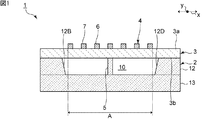
図1は、本発明の第1の実施形態に係る弾性波装置の正面断面図である。図2は第1の実施形態に係る弾性波装置の平面図である。なお、図1は、図2中のI−I線に沿う断面図である。図2においては、後述する支持部材をハッチングにより示す。図2以外の平面図においても同様である。 FIG. 1 is a front sectional view of an elastic wave device according to a first embodiment of the present invention. FIG. 2 is a plan view of the elastic wave device according to the first embodiment. Note that FIG. 1 is a cross-sectional view taken along the line I-I in FIG. In FIG. 2, the support member described later is shown by hatching. The same applies to the plan views other than FIG. 2.
図1に示すように、弾性波装置1は支持基板2、圧電膜3、機能電極4及び支持部材5を有する。支持基板2上に圧電膜3が設けられている。圧電膜3上に機能電極4が設けられている。支持部材5は圧電膜3を支持している。
As shown in FIG. 1, the
支持基板2は空洞部10、支持部12及び底部13を有する。支持部12は枠状の形状を有する。支持部12は底部13上に設けられている。空洞部10は、支持基板2に設けられた凹部である。より具体的には、空洞部10は、支持部12及び底部13に囲まれた凹部である。空洞部10は、圧電膜3側において開口している。なお、図1における破線は、支持基板2の底部13と支持部12との境界及び支持基板2と支持部材5との境界を模式的に示す。
The
図2に示すように、支持部12は、第1の内側面12A、第2の内側面12B、第3の内側面12C及び第4の内側面12Dを含む。第1の内側面12A及び第3の内側面12Cは対向し合っている。第2の内側面12B及び第4の内側面12Dは対向し合っている。第1の内側面12Aの両端は、第2の内側面12B及び第4の内側面12Dに接続されている。同様に、第3の内側面12Cの両端は、第2の内側面12B及び第4の内側面12Dに接続されている。
As shown in FIG. 2, the
支持基板2はシリコン基板である。支持基板2の圧電膜3側の面における面方位は(100)、(110)または(111)であることが好ましい。支持基板2の抵抗率は4kΩ以上であることが好ましい。もっとも、支持基板2の材料は上記に限定されず、例えば、酸化アルミニウム、タンタル酸リチウム、ニオブ酸リチウム、水晶などの圧電体、アルミナ、マグネシア、サファイア、窒化ケイ素、窒化アルミニウム、炭化ケイ素、ジルコニア、コージライト、ムライト、ステアタイト、フォルステライトなどの各種セラミック、ダイヤモンド、ガラスなどの誘電体、シリコン、窒化ガリウムなどの半導体などを用いることができる。
The
支持基板2の支持部12上に、空洞部10を覆うように、圧電膜3が設けられている。圧電膜3は第1の主面3a及び第2の主面3bを有する。第1の主面3a及び第2の主面3bは対向し合っている。第1の主面3a及び第2の主面3bのうち、第2の主面3bが支持基板2側の主面である。本実施形態では、圧電膜3はニオブ酸リチウム膜である。より具体的には、圧電膜3はLiNbO3膜である。なお、圧電膜3の材料は上記に限定されず、例えば、LiTaO3などのタンタル酸リチウムを用いてもよい。圧電膜3の厚みは40nm以上、1000nm以下であることが好ましい。A
図2に示すように、圧電膜3の第1の主面3a上に機能電極4が設けられている。機能電極4は複数の電極を有する。複数の電極は、圧電膜3の厚み方向に交叉する方向に並んでいる。各電極は矩形形状を有する。複数の電極は、複数対の第1電極6及び第2電極7を含む。本実施形態においては、第1電極6及び第2電極7は平行に延びている。第1電極6が延びる方向と直交する方向において、隣り合う第1電極6及び第2電極7が対向している。以下においては、第1電極6が延びる方向をy方向とし、y方向と直交する方向をx方向とする。x方向及びy方向の双方は、圧電膜3の厚み方向と交叉する方向である。このため、隣り合う第1電極6及び第2電極7は、圧電膜3の厚み方向に交叉する方向において対向しているともいえる。ここで、本明細書において、「直交」とは、厳密に直交する場合のみに限定されず、略直交を含む。略直交とは、本明細書においては、例えば90°±10°の範囲内の角度をいうものとする。
As shown in FIG. 2, the
機能電極4は第1のバスバー8及び第2のバスバー9を有する。第1のバスバー8及び第2のバスバー9は対向し合っている。複数の第1電極6の一方端が、それぞれ第1のバスバー8に接続されている。複数の第2電極7の一方端が、それぞれ第2のバスバー9に接続されている。複数の第1電極6及び複数の第2電極7は、互いに間挿し合っている。第1電極6及び第2電極7は、互いに異なる電位に接続される。
The
機能電極4は、Al、AlCu合金などの適宜の金属もしくは合金からなる。AlCu合金におけるCuは、1重量%以上、10重量%以下であることが好ましい。機能電極4は、積層金属膜からなっていてもよい。この場合、例えば、密着層を有していてもよい。密着層としては、例えば、Ti層やCr層などが挙げられる。
The
図2に示すように、機能電極4は交叉領域Aを有する。交叉領域Aは、x方向から見て、隣り合う電極が重なっている領域である。交叉領域Aは、x方向における、機能電極4の最も外側の電極のうちの一方の電極から、最も外側の電極のうちの他方の電極に至る領域である。なお、交叉領域Aは、上記最も外側の電極の、x方向における外側の端部を含む。
As shown in FIG. 2, the
図3は、第1の実施形態の支持基板における空洞部の内部及び圧電膜上の構成を示すための、弾性波装置の一部を示す模式的斜視図である。図3においては、空洞部10の輪郭を破線により示す。
FIG. 3 is a schematic perspective view showing a part of an elastic wave device for showing the structure inside the cavity and on the piezoelectric film in the support substrate of the first embodiment. In FIG. 3, the outline of the
支持基板2の空洞部10内に、1個の支持部材5が配置されている。平面視において、支持部材5は交叉領域Aと重なっている。本明細書において平面視とは、図1または図3における上方から見る方向をいう。支持部材5は、平面視において、1本のみの第2電極7と重なっている。より具体的には、支持部材5は、平面視において、圧電膜3における、第2電極7が設けられている領域のみと重なっている。
One
図2に示すように、支持部材5は空洞部10を横断しており、空洞部10を分割している。支持部材5は、支持基板2の支持部12に接続されている。より具体的には、支持部材5は、支持基板2の第1の内側面12A及び第3の内側面12Cに接続されている。このように、支持部材5は壁状である。もっとも、支持部材5は支持部12に接続されていなくともよい。
As shown in FIG. 2, the
弾性波装置1の支持部材5はシリコンからなる。図1に示すように、支持部材5は、支持基板2と一体として設けられている。より具体的には、支持部材5は、支持基板2の底部13から圧電膜3側に突出している。支持部材5は圧電膜3に直接的に接触している。これにより、支持部材5は、圧電膜3を支持している。
The
本実施形態の特徴は、支持部材5が、平面視において、交叉領域Aと重なるように、空洞部10に配置されていることにある。これにより、支持基板2に空洞部10が設けられている場合においても、支持部材5により圧電膜3を支持することができる。よって、弾性波装置1の構造的な脆弱性が生じ難い。
A feature of this embodiment is that the
ところで、本実施形態においては、圧電膜3上に反射器は設けられていない。弾性波装置1は反射器を有しない。あるいは、弾性波装置1が反射器を有する場合には、反射器の電極指の本数を少なくすることができる。これは、弾性波装置1が厚み滑り1次モードのバルク波を利用していることによる。以下において、弾性波装置1が利用している厚み滑り1次モードの詳細を説明する。
By the way, in this embodiment, the reflector is not provided on the
図2に示すように、隣り合う1対の第1電極6及び第2電極7の構造が、x方向に、複数対設けられている。この対数は、整数対である必要はなく、1.5対や2.5対などであってもよい。なお、機能電極4における電極が隣り合うとは、電極同士が直接接触するように配置されている場合ではなく、電極同士が間隔を介して配置されている場合を指す。また、第1電極6と第2電極7とが隣り合う場合、第1電極6と第2電極7との間には、他のホット電極またはグラウンド電極は配置されない。
As shown in FIG. 2, a plurality of pairs of adjacent
弾性波装置1の駆動に際しては、複数の第1電極6と、複数の第2電極7との間に交流電圧を印加する。より具体的には、第1のバスバー8と第2のバスバー9との間に交流電圧を印加する。それによって、圧電膜3において励振される厚み滑り1次モードのバルク波を利用した、共振特性を得ることが可能とされている。このように、第1電極6と第2電極7との間の領域は励振領域Bである。図2においては、例として1つの励振領域Bを示しているが、複数の第1電極6と複数の第2電極7との間の領域は、いずれも励振領域Bである。励振領域Bは交叉領域Aに含まれる。
When driving the
弾性波装置1では、圧電膜3の厚みをd、複数対の第1電極6及び第2電極7のうちいずれかの隣り合う第1電極6及び第2電極7の中心間距離をpとした場合、d/pは0.5以下とされている。そのため、上記厚み滑り1次モードのバルク波が効果的に励振され、良好な共振特性を得ることができる。ここで、第1電極6及び第2電極7の中心間距離とは、第1電極6のx方向における中心と、第2電極7のx方向における中心とを結んだ距離となる。
In the
弾性波装置1は上記構成を備え、厚み滑り1次モードを利用している。それによって、第1電極6及び第2電極7の対数を少なくしたとしても、Q値の低下が生じ難い。
The
本実施形態では、圧電膜3にZカットの圧電体を用いている。そのため、x方向は、圧電膜3の分極方向と直交する方向となる。圧電膜3に他のカット角の圧電体を用いた場合には、この限りでない。
In this embodiment, a Z-cut piezoelectric material is used for the
厚み滑り1次モードのバルク波と、従来利用されているラム波との相違を、図4(a)及び図4(b)を参照して説明する。 The difference between the bulk wave in the thickness slip primary mode and the conventionally used ram wave will be described with reference to FIGS. 4 (a) and 4 (b).
図4(a)は、特許文献1に記載のような弾性波装置の圧電膜を伝搬するラム波を説明するための模式的正面断面図である。ここでは、圧電膜201中を矢印で示すように波が伝搬する。ここで、圧電膜201では、第1の主面201aと、第2の主面201bとが対向しており、第1の主面201aと第2の主面201bとを結ぶ厚み方向がz方向である。x方向は、IDT電極の電極指が並んでいる方向である。図4(a)に示すように、ラム波はx方向に伝搬していく。ラム波は板波であるため、圧電膜201が全体として振動するものの、波はx方向に伝搬する。そのため、IDT電極のx方向両側に反射器を配置して、共振特性を得ている。
FIG. 4A is a schematic front sectional view for explaining a Lamb wave propagating in a piezoelectric film of an elastic wave device as described in
これに対して、図4(b)に示すように、本実施形態の弾性波装置では、振動変位は厚み滑り方向である。そのため、波はz方向にほぼ伝搬し、共振する。よって、波のx方向成分がz方向成分に比べて著しく小さい。そして、このz方向の波の伝搬により共振特性が得られるため、反射器の電極指の本数を少なくしても、伝搬損失は生じ難い。さらに、小型化を進めようとして、第1電極6及び第2電極7からなる電極対の対数を減らしたとしても、Q値の低下が生じ難い。
On the other hand, as shown in FIG. 4B, in the elastic wave device of the present embodiment, the vibration displacement is in the thickness slip direction. Therefore, the wave propagates almost in the z direction and resonates. Therefore, the x-direction component of the wave is significantly smaller than the z-direction component. Since the resonance characteristic is obtained by the propagation of the wave in the z direction, the propagation loss is unlikely to occur even if the number of electrode fingers of the reflector is reduced. Further, even if the logarithm of the electrode pair composed of the
なお、厚み滑り1次モードのバルク波の振幅方向は、図5に示すように、圧電膜3の励振領域に含まれる第1領域451と、励振領域に含まれる第2領域452とにおいて逆になる。図5では、第1電極6と第2電極7との間に、第2電極7が第1電極6よりも高電位となる電圧が印加された場合のバルク波を模式的に示してある。第1領域451は、励振領域のうち、圧電膜3の厚み方向に直交し圧電膜3を2分する仮想平面VP1と、第1の主面3aとの間の領域である。第2領域452は、励振領域のうち、仮想平面VP1と、第2の主面3bとの間の領域である。
As shown in FIG. 5, the amplitude direction of the bulk wave in the thickness slip primary mode is opposite in the
上記のように、弾性波装置1では、複数対の第1電極6及び第2電極7が配置されている。厚み滑り1次モードは、x方向に波を伝搬させるものではないため、第1電極6及び第2電極7からなる電極対は複数対設けられている必要はない。すなわち、少なくとも1対の第1電極6及び第2電極7が設けられてさえおればよい。
As described above, in the
弾性波装置1においては、第1電極6がホット電位に接続される電極であり、第2電極7がグラウンド電位に接続される電極である。もっとも、第1電極6がグラウンド電位に接続され、第2電極7がホット電位に接続されてもよい。本実施形態では、少なくとも1対の電極は、上記のように、ホット電位に接続される電極またはグラウンド電位に接続される電極であり、浮き電極は設けられていない。
In the
ところで、本実施形態では、d/pは0.5以下である。d/pは0.24以下であることが好ましい。その場合には、より一層良好な共振特性を得ることができる。これを、図6を参照して説明する。 By the way, in this embodiment, d / p is 0.5 or less. The d / p is preferably 0.24 or less. In that case, even better resonance characteristics can be obtained. This will be described with reference to FIG.
d/pを変化させ、複数の弾性波装置を得た。図6は、このd/pと、弾性波装置の共振子としての比帯域との関係を示す図である。 A plurality of elastic wave devices were obtained by changing d / p. FIG. 6 is a diagram showing the relationship between this d / p and the specific band as a resonator of the elastic wave device.
図6から明らかなように、d/p>0.5では、d/pを調整しても、比帯域は5%未満である。これに対して、d/p≦0.5の場合には、その範囲内でd/pを変化させれば、比帯域を5%以上とすることができる。よって、高い結合係数を有する共振子を構成することができる。また、d/pが0.24以下の場合には、比帯域を7%以上と高めることができる。加えて、d/pをこの範囲内で調整すれば、比帯域がより一層広い共振子を得ることができ、より一層高い結合係数を有する共振子を実現することができる。なお、例えば、圧電膜3が厚みばらつきを有する場合には、その厚みを平均化した値を採用してもよい。
As is clear from FIG. 6, when d / p> 0.5, the ratio band is less than 5% even if the d / p is adjusted. On the other hand, in the case of d / p ≦ 0.5, the ratio band can be set to 5% or more by changing d / p within that range. Therefore, it is possible to construct a resonator having a high coupling coefficient. Further, when d / p is 0.24 or less, the specific band can be increased to 7% or more. In addition, if the d / p is adjusted within this range, a resonator having a wider specific band can be obtained, and a resonator having a higher coupling coefficient can be realized. For example, when the
隣り合う第1電極6及び第2電極7の中心間距離pは、1μm以上、10μm以下であることが好ましい。機能電極4の複数の電極のx方向に沿う寸法を幅としたときに、第1電極6及び第2電極7の幅は、それぞれ、50nm以上、1000nm以下であることが好ましい。
The distance p between the centers of the adjacent
ここで、図1に示すように、第1の実施形態における支持部材5は、平面視において、第2電極7が設けられている領域のみと重なっている。それによって、共振特性をほぼ劣化させずして、弾性波装置1の構造的な脆弱性が生じることを抑制できる。この詳細を、第1の実施形態と比較例とを比較することにより、以下において説明する。なお、比較例は、支持部材を有しない点において第1の実施形態と異なる。
Here, as shown in FIG. 1, the
第1の実施形態及び比較例の弾性波装置を用意し、インピーダンス周波数特性を比較した。用意した第1の実施形態の弾性波装置の設計パラメータは以下の通りである。ここで、支持部材5のx方向に沿う寸法を支持部材5の幅とする。比較例の設計パラメータは、支持部材5以外においては、第1の実施形態の設計パラメータと同様である。
The elastic wave devices of the first embodiment and the comparative example were prepared, and the impedance frequency characteristics were compared. The design parameters of the prepared elastic wave device of the first embodiment are as follows. Here, the dimension of the
圧電膜3;材料…LiNbO3、厚み400nm
第1電極6及び第2電極7からなる電極対の対数=50対
支持基板2;材料…Si
支持部材5;材料…Si、幅1.012μm
第1電極6及び第2電極7の中心間距離p;3.75μm
第1電極6及び第2電極7の幅;1.012μm
d/p;0.27
Logarithm of electrode pair consisting of
Distance between the centers of the
Width of
d / p; 0.27
図7は、第1の実施形態及び比較例の弾性波装置のインピーダンス周波数特性を示す図である。 FIG. 7 is a diagram showing impedance frequency characteristics of the elastic wave device of the first embodiment and the comparative example.
図7に示すように、第1の実施形態のインピーダンス周波数特性は、比較例のインピーダンス周波数特性とほぼ変わらないことがわかる。第1の実施形態においては、厚み滑り1次モードを利用している。この場合、圧電膜3における、第1電極6及び第2電極7の間に位置する、励振領域Bにおいて変位が大きい。他方、圧電膜3における、第1電極6及び第2電極7が設けられている部分においては変位が小さい。弾性波装置1の支持部材5は、平面視において、第2電極7が設けられている領域のみと重なっている。よって、支持部材5は、圧電膜3の変位が小さい部分にのみ接触しているため、圧電膜3の変位を阻害し難い。従って、共振特性をほぼ劣化させずして、弾性波装置1の構造的な脆弱性が生じることを抑制できる。同様に、支持部材5が、平面視において、第1電極6が設けられている領域のみと重なっている場合においても、共振特性をほぼ劣化させずして、弾性波装置1の構造的な脆弱性が生じることを抑制できる。
As shown in FIG. 7, it can be seen that the impedance frequency characteristics of the first embodiment are almost the same as the impedance frequency characteristics of the comparative example. In the first embodiment, the thickness slip primary mode is used. In this case, the displacement is large in the excitation region B located between the
支持部材5と圧電膜3とが平面視において重なっている面積は、機能電極4の1本の電極と圧電膜3とが平面視において重なっている面積よりも小さいことが好ましい。この場合には、圧電膜3の変位をより確実に阻害し難い。もっとも、支持部材5は、平面視において、交叉領域Aと重なっていればよい。
The area where the
第1の実施形態においては、空洞部10のy方向に沿う寸法は、交叉領域Aのy方向に沿う寸法と同じである。弾性波装置1の支持部材5は、平面視において、第2電極7における交叉領域Aに位置する部分のみと重なっている。なお、空洞部10の配置は上記に限定されない。平面視において、交叉領域A全体が空洞部10と重なっていればよい。空洞部10のy方向に沿う寸法は、交叉領域Aのy方向に沿う寸法以上であればよい。それによって、機能電極4に電圧を印加した際の圧電膜3の変位が阻害され難い。
In the first embodiment, the dimension of the
第1の実施形態においては、第1のバスバー8及び第2のバスバー9は、第1電極6及び第2電極7が対向している方向と平行に延びている。なお、機能電極4の形状はこれに限定されない。例えば、第1のバスバー8及び第2のバスバー9は、第1電極6及び第2電極7が対向している方向と垂直に延びていてもよい。この場合には、第1電極6及び第2電極7の形状は、例えば、L字状などであってもよい。
In the first embodiment, the
以下において、第1の実施形態の各変形例を示す。各変形例においても、第1の実施形態と同様に、弾性波装置の構造的な脆弱性が生じ難い。 Hereinafter, each modification of the first embodiment will be shown. In each modification, as in the first embodiment, structural fragility of the elastic wave device is unlikely to occur.
図8〜図10において、第1〜第3の変形例を示す。第1〜第3の変形例においては、支持部材の形状のみが第1の実施形態と異なる。図8に示す第1の変形例においては、支持部材25Aの幅は第2電極7の幅よりも狭い。
8 to 10 show the first to third modification examples. In the first to third modifications, only the shape of the support member is different from the first embodiment. In the first modification shown in FIG. 8, the width of the
図9に示す第2の変形例においては、支持部材25Bは角柱状である。支持部材25Bは、支持基板2の支持部12には接続されていない。支持部材25Bの幅は、第2電極7の幅よりも広い。支持部材25Bと圧電膜3とが平面視において重なっている面積は、機能電極4の1本の電極と圧電膜3とが平面視において重なっている面積よりも小さい。支持部材25Bは、平面視において、第2電極7と、励振領域Bとに重なっている。なお、支持部材25Bは、平面視において、励振領域Bのx方向における中央Cよりも、第2電極7に近い部分と重なっている。
In the second modification shown in FIG. 9, the
図10に示す第3の変形例においては、支持部材25Cは円柱状である。支持部材25Cは、支持基板2の支持部12には接続されていない。
In the third modification shown in FIG. 10, the
第1の実施形態においては、1個の支持部材5が設けられている。なお、複数の支持部材が設けられていてもよい。この例を、以下の第1の実施形態の第4の変形例及び第5の変形例により示す。
In the first embodiment, one
図11に示す第4の変形例においては、支持基板2の空洞部10に複数の支持部材25Dが配置されている。各支持部材25Dは角柱状である。複数の支持部材25Dは、平面視において、同じ第2電極7と重なっている。複数の支持部材25Dは、圧電膜3における、第2電極7が設けられている領域のみと重なっている。
In the fourth modification shown in FIG. 11, a plurality of
図12に示す第5の変形例においては、支持基板2の空洞部10に複数の支持部材25Eが配置されている。各支持部材25Eは壁状である。複数の支持部材25Eは、平面視において、互いに異なる第2電極7と重なっている。複数の支持部材25Eは、圧電膜3における、第2電極7が設けられている領域のみと重なっている。本変形例においては、複数の支持部材25Eは、それぞれ、支持基板2の第1の内側面12A及び第3の内側面12Cに接続されている。もっとも、少なくとも1個の支持部材25Eは、第1の内側面12Aまたは第3の内側面12Cに接続されていなくともよい。
In the fifth modification shown in FIG. 12, a plurality of
本変形例においては、複数の支持部材25Eが、平面視において、全ての第2電極7と重なっている。なお、例えば、平面視において、1個の支持部材25Eが第1電極6と重なっており、他の1個の支持部材25Eが第2電極7と重なっていてもよい。複数の支持部材25Eのそれぞれの配置は上記に限定されない。複数の支持部材25Eは、平面視において、交叉領域Aと重なっていればよい。
In this modification, the plurality of
図13は、第1の実施形態の第6の変形例に係る弾性波装置の正面断面図である。 FIG. 13 is a front sectional view of the elastic wave device according to the sixth modification of the first embodiment.
本変形例においては、支持部材5の圧電膜3側の面上には、絶縁膜26が設けられている。支持部材5は、圧電膜3に、絶縁膜26を介して間接的に接触している。このように、支持部材5は、圧電膜3に直接的に接触していなくともよい。支持基板2における支持部12上には、絶縁膜27が設けられている。支持基板2は、圧電膜3に、絶縁膜27を介して間接的に接触している。このように、支持基板2は、圧電膜3に直接的に接触していなくともよい。絶縁膜26及び絶縁膜27は酸化ケイ素膜である。もっとも、絶縁膜26及び絶縁膜27の材料は上記に限定されず、例えば、窒化ケイ素、酸窒化ケイ素またはアルミナなどの適宜の絶縁性材料を用いることができる。
In this modification, the insulating
なお、支持部材5及び支持基板2のうちの一方が圧電膜3に直接的に接していてもよい。あるいは、絶縁膜26及び絶縁膜27が一体の絶縁膜として構成されていてもよい。
One of the
図14は、第1の実施形態の第7の変形例に係る弾性波装置の正面断面図である。 FIG. 14 is a front sectional view of the elastic wave device according to the seventh modification of the first embodiment.
本変形例においては、支持部材25Fは、支持基板2と別体として設けられている。支持部材25Fは、適宜の金属からなる。なお、支持部材25Fは、適宜の半導体または絶縁体などからなっていてもよい。第6の変形例と同様に、支持基板2における支持部12と圧電膜3との間に、絶縁膜27が設けられている。もっとも、支持基板2と圧電膜3とは直接的に接触していてもよい。
In this modification, the
支持部材25Fの熱伝導率は、圧電膜3の熱伝導率以上であることが好ましい。それによって、弾性波を励振した際に生じる熱などが、圧電膜3から支持部材25Fに伝導し易い。圧電膜3から支持部材25Fに伝導した熱は、さらに支持基板2側に放熱される。よって、放熱性を高めることができる。本変形例のように、支持部材25Fが金属からなることがより好ましい。この場合には、支持部材25Fの熱伝導率を好適に高くすることができ、放熱性をより確実に高めることができる。
The thermal conductivity of the
図14に示すように、支持部材25Fは、圧電膜3と直接的に接触している。それによって、放熱性を効果的に高めることができる。なお、第6の変形例と同様に、支持部材25Fと圧電膜3との間に絶縁膜26が設けられていてもよい。
As shown in FIG. 14, the
図15は、第2の実施形態に係る弾性波装置の平面図である。 FIG. 15 is a plan view of the elastic wave device according to the second embodiment.
本実施形態は、空洞部10のy方向に沿う寸法が、交叉領域Aのy方向に沿う寸法よりも大きい点、及び支持部材35の配置が第1の実施形態と異なる。上記の点以外においては、本実施形態の弾性波装置は第1の実施形態の弾性波装置1と同様の構成を有する。
The present embodiment is different from the first embodiment in that the dimension of the
空洞部10のy方向に沿う寸法は、機能電極4のy方向に沿う寸法よりも大きい。平面視において、支持基板2の支持部12は、機能電極4を囲んでいる。よって、平面視において、機能電極4の全体が空洞部10と重なっている。
The dimension of the
支持部材35は、支持基板2の第1の内側面12A及び第3の内側面12Cに接続されている。よって、支持部材35は、平面視において、第1のバスバー8及び第2のバスバー9と重なっている。さらに、支持部材35は、平面視において、圧電膜3の機能電極4が設けられている部分よりもy方向における外側の部分と重なっている。
The
本実施形態においても、第1の実施形態と同様に、弾性波装置の構造上の脆弱性が生じ難い。なお、空洞部10のy方向に沿う寸法が交叉領域Aのy方向に沿う寸法よりも大きい場合においても、支持部材35の配置は上記に限定されない。例えば、支持部材35の配置は、第1の実施形態やその各変形例と同様の配置であってもよい。
Also in this embodiment, as in the first embodiment, structural fragility of the elastic wave device is unlikely to occur. Even when the dimension of the
図16は、第3の実施形態の支持基板における空洞部の内部及び圧電膜上の構成を示すための、弾性波装置の一部を示す模式的斜視図である。 FIG. 16 is a schematic perspective view showing a part of an elastic wave device for showing the structure inside the cavity and on the piezoelectric film in the support substrate of the third embodiment.
本実施形態は、機能電極44における複数の電極の配置、及び機能電極44と支持部材5との位置関係が第1の実施形態と異なる。上記の点以外においては、本実施形態の弾性波装置は第1の実施形態の弾性波装置1と同様の構成を有する。
The present embodiment is different from the first embodiment in the arrangement of the plurality of electrodes in the
機能電極44は、第1電極6同士が隣り合っている部分を有する。圧電膜3における、隣り合う第1電極6が設けられている部分の間の部分は、非励振領域Dである。本実施形態では、隣り合う第1電極6同士の中心間距離は2pである。非励振領域Dにおいては、厚み滑り1次モードのバルク波は励振されない。非励振領域Dは交叉領域Aに含まれる。
The
なお、隣り合う第1電極6同士の中心間距離は2p±0.5pの範囲内であることが好ましい。この範囲内であれば、共振特性の劣化はほぼ生じない。
The distance between the centers of the adjacent
支持部材5は、平面視において、非励振領域Dと重なっている。非励振領域Dにおいては、圧電膜3の変位は小さい。よって、本実施形態においては、支持部材5により圧電膜3を支持していても、圧電膜3の変位を阻害し難い。従って、共振特性をほぼ劣化させずして、弾性波装置の構造的な脆弱性が生じることを抑制できる。
The
図16に示す本実施形態のように、支持部材5は、平面視において、隣り合う2つの第1電極6の間の、非励振領域Dの中央と重なっていることが好ましい。非励振領域Dのx方向における中央は、励振領域Bからの距離が長いため、圧電膜3の変位がより一層小さい。よって、支持部材5により圧電膜3を支持していても、圧電膜3の変位をより一層阻害し難い。
As in the present embodiment shown in FIG. 16, it is preferable that the
本実施形態及び第1の実施形態においては、厚み滑り1次モードを利用している。これにより、本実施形態の弾性波装置が非励振領域Dを有するにも関わらず、本実施形態と第1の実施形態とにおいて、共振特性にほぼ変化がない。 In the present embodiment and the first embodiment, the thickness slip primary mode is used. As a result, although the elastic wave device of the present embodiment has the non-excitation region D, there is almost no change in the resonance characteristics between the present embodiment and the first embodiment.
図17は、第4の実施形態に係る弾性波装置の正面断面図である。 FIG. 17 is a front sectional view of the elastic wave device according to the fourth embodiment.
本実施形態は、機能電極44が圧電膜3の第2の主面3b上に設けられている点、及び平面視において、支持基板2の支持部12が機能電極44を囲んでいる点において、第3の実施形態と異なる。上記の点以外においては、本実施形態の弾性波装置は第3の実施形態の弾性波装置と同様の構成を有する。
In this embodiment, the
支持部材5は、隣り合う第1電極6間に配置されている。支持部材5は、平面視において、交叉領域Aにおける非励振領域Dと重なっている。よって、第3の実施形態と同様に、共振特性をほぼ劣化させずして、弾性波装置の構造的な脆弱性が生じることを抑制できる。
The
図18は、第5の実施形態に係る弾性波装置の正面断面図である。図19は、第5の実施形態に係る弾性波装置の平面図である。 FIG. 18 is a front sectional view of the elastic wave device according to the fifth embodiment. FIG. 19 is a plan view of the elastic wave device according to the fifth embodiment.
図18及び図19に示すように、本実施形態は、支持部材55が、第2電極7と同種の材料からなり、第2電極7と同じ電位に接続される点において、第4の実施形態と異なる。上記の点以外においては、本実施形態の弾性波装置は第4の実施形態の弾性波装置と同様の構成を有する。
As shown in FIGS. 18 and 19, in the fourth embodiment, the
図19に示すように、支持部材55は第2のバスバー9に接続されている。支持部材55は、圧電膜3に直接的に接触している。これにより、支持部材55は、第2電極7と同様に、厚み滑り1次モードのバルク波の励振に寄与する。より具体的には、隣り合う第1電極6及び支持部材55の間に交流電圧が印加されることにより、厚み滑り1次モードのバルク波が励振される。よって、本実施形態においては、隣り合う第1電極6のうちの一方と支持部材55との間の領域は励振領域Bである。同様に、隣り合う第1電極6のうちの他方と支持部材55との間の領域も励振領域Bである。上述したように、機能電極44の各電極は積層金属膜からなっていてもよい。この場合、支持部材55も積層金属膜からなっていてもよい。
As shown in FIG. 19, the
圧電膜3における、支持部材55が接触している部分においては、厚み滑り1次モードのバルク波はほとんど励振されない。よって、圧電膜3の変位は阻害され難い。本実施形態においても、共振特性を劣化させ難く、かつ弾性波装置の構造的な脆弱性が生じることを抑制できる。なお、支持部材55は、第1電極6と同種の材料からなり、第1電極6と同じ電位に接続されてもよい。この場合、支持部材55は、第1のバスバー8に接続されていてもよい。なお、本実施形態では、第1電極6及び第2電極7は同種の材料により構成されている。
In the portion of the
本実施形態の弾性波装置の製造に際しては、例えば、圧電膜3上に機能電極44及び支持部材55を形成した後に、圧電膜3と支持基板2とを接合してもよい。機能電極44及び支持部材55は、例えば、リフトオフ法などにより形成することができる。以下において、支持部材55及び機能電極44の形成の方法の一例を説明する。
In the manufacture of the elastic wave device of the present embodiment, for example, the
図20(a)〜図20(c)は、第5の実施形態における機能電極及び支持部材を形成する方法の一例を説明するための正面断面図である。図21(a)〜図21(c)は、第5の実施形態における支持部材を形成する方法の一例を説明するための正面断面図である。 20 (a) to 20 (c) are front sectional views for explaining an example of the method of forming the functional electrode and the support member in the fifth embodiment. 21 (a) to 21 (c) are front sectional views for explaining an example of the method of forming the support member in the fifth embodiment.
図20(a)に示すように、圧電膜3上にレジストパターン53Aを形成する。レジストパターン53Aは、機能電極44及び支持部材55の形状の開口部を有する。レジストパターン53Aの形成に際しては、例えば、印刷法などによりレジスト層を形成する。次に、例えば、露光及び現像によりパターニングすればよい。
As shown in FIG. 20A, a resist
次に、図20(b)に示すように、圧電膜3上及びレジストパターン53A上に、機能電極44及び支持部材55用の金属層54Aを形成する。なお、金属層54Aは、単層の金属膜であってもよく、積層金属膜であってもよい。金属層54Aは、例えば、スパッタリング法または真空蒸着法などにより形成することができる。次に、レジストパターン53Aを、例えばエッチングなどにより剥離する。これにより、図20(c)に示すように、機能電極44を得る。
Next, as shown in FIG. 20B, a
次に、図21(a)に示すように、圧電膜3上に、機能電極44を覆うように、レジストパターン53Bを形成する。レジストパターン53Bは、支持部材55の形状の開口部を有する。レジストパターン53Bは、上記レジストパターン53Aと同様にして形成することができる。
Next, as shown in FIG. 21A, a resist
次に、図21(b)に示すように、金属層54A上及びレジストパターン53B上に、支持部材55用の金属層54Bを形成する。図21(b)中の破線は、金属層54A及び金属層54Bの境界を模式的に示す。金属層54A及び金属層54Bは、それぞれ、単層の金属膜であってもよく、積層金属膜であってもよい。次に、レジストパターン53Bを剥離する。これにより、図21(c)に示すように、支持部材55を得る。
Next, as shown in FIG. 21B, the
図22は、第5の実施形態の変形例に係る弾性波装置の正面断面図である。 FIG. 22 is a front sectional view of the elastic wave device according to the modified example of the fifth embodiment.
本変形例においては、複数の支持部材65A及び支持部材65Bが設けられている。図22においては、2個ずつの支持部材65A及び支持部材65Bが示されている。もっとも、支持部材65A及び支持部材65Bの個数は上記に限定されない。
In this modification, a plurality of
支持部材65Aは、第1電極6と同種の材料からなり、第1電極6と同じ電位に接続される。支持部材65Aは第1のバスバー8に接続されている。他方、支持部材65Bは、第2電極7と同種の材料からなり、第2電極7と同じ電位に接続される。支持部材65Bは第2のバスバー9に接続されている。本変形例においても、弾性波装置の構造的な脆弱性が生じ難い。
The
隣り合う第1電極6及び第2電極7の間に交流電圧が印加される場合と同様に、隣り合う支持部材65A及び第2電極7の間に交流電圧が印加されることにより、厚み滑り1次モードのバルク波が励振される。隣り合う第1電極6及び支持部材65Bの間に交流電圧が印加されることによっても、厚み滑り1次モードのバルク波が励振される。さらに、隣り合う支持部材65A及び支持部材65Bの間に交流電圧が印加されることによっても、厚み滑り1次モードのバルク波が励振される。このように複数の支持部材65A及び支持部材65Bが、厚み滑り1次モードのバルク波の励振に寄与してもよい。
Similar to the case where an AC voltage is applied between the adjacent
図23は、第6の実施形態に係る弾性波装置の平面図である。図24は、第6の実施形態に係る弾性波装置の正面断面図である。 FIG. 23 is a plan view of the elastic wave device according to the sixth embodiment. FIG. 24 is a front sectional view of the elastic wave device according to the sixth embodiment.
図23及び図24に示す弾性波装置71は、板波を利用している。本実施形態における圧電膜3は、窒化アルミニウム膜である。より具体的には、圧電膜3はAlN膜である。なお、圧電膜3の材料は上記に限定されず、例えば、タンタル酸リチウムまたはニオブ酸リチウムなどであってもよい。
The
弾性波装置71における機能電極は、IDT電極74である。IDT電極74は、第1のバスバー78、第2のバスバー79、複数の第1の電極指76及び複数の第2の電極指77を有する。複数の第1の電極指76は、本発明における複数の第1電極である。複数の第2の電極指77は、本発明における複数の第2電極である。複数の第1の電極指76の一方端は、それぞれ第1のバスバー78に接続されている。複数の第2の電極指77の一方端は、それぞれ第2のバスバー79に接続されている。複数の第1の電極指76及び複数の第2の電極指77は互いに間挿し合っている。よって、隣り合う第1の電極指76及び第2の電極指77は、x方向において対向し合っている。IDT電極74は、第1の実施形態における機能電極4と同様に、交叉領域Aを有する。本実施形態では、交叉領域A自体が励振領域である。
The functional electrode in the
圧電膜3上におけるIDT電極74のx方向両側には、一対の反射器72A及び反射器72Bが設けられている。弾性波装置71においては、平面視において、支持基板2の支持部12が、IDT電極74並びに一対の反射器72A及び反射器72Bを囲んでいる。よって、平面視において、IDT電極74並びに一対の反射器72A及び反射器72Bの全体が空洞部10と重なっている。
A pair of
支持部材5は、平面視において、第2の電極指77と重なっている。もっとも、支持部材5は、平面視において、交叉領域Aと重なっていればよい。本実施形態においても、弾性波装置71の構造上の脆弱性が生じ難い。
The
1…弾性波装置
2…支持基板
3…圧電膜
3a…第1の主面
3b…第2の主面
4…機能電極
5…支持部材
6,7…第1,第2電極
8,9…第1,第2のバスバー
10…空洞部
12…支持部
12A〜12D…第1〜第4の内側面
13…底部
25A〜25F…支持部材
26,27…絶縁膜
35…支持部材
44…機能電極
53A,53B…レジストパターン
54A,54B…金属層
55…支持部材
65A,65B…支持部材
71…弾性波装置
72A,72B…反射器
74…IDT電極
76,77…第1,第2の電極指
78,79…第1,第2のバスバー
201…圧電膜
201a,201b…第1,第2の主面
451,452…第1,第2領域
VP1…仮想平面1 ...
Claims (13)
前記空洞部を覆うように、前記支持基板上に設けられている圧電膜と、
平面視において前記空洞部と重なるように、前記圧電膜上に設けられている機能電極と、
前記支持基板の前記空洞部に配置されており、前記圧電膜を支持している支持部材と、を備え、
前記機能電極が、前記圧電膜の厚み方向に交叉する方向に並んでいる複数の電極を有し、
前記複数の電極が、前記圧電膜の厚み方向に交叉する方向において対向しており、かつ互いに異なる電位に接続される第1電極及び第2電極を含み、
前記第1電極が延びる方向と直交する方向から見て、隣り合う前記電極が重なっている領域が交叉領域であり、平面視において、前記交叉領域と前記支持部材とが重なっている、弾性波装置。A support board with a cavity and
A piezoelectric film provided on the support substrate so as to cover the cavity,
A functional electrode provided on the piezoelectric film so as to overlap the cavity in a plan view,
A support member arranged in the cavity of the support substrate and supporting the piezoelectric film is provided.
The functional electrode has a plurality of electrodes arranged in a direction intersecting with each other in the thickness direction of the piezoelectric film.
The plurality of electrodes include a first electrode and a second electrode that face each other in a direction intersecting with each other in the thickness direction of the piezoelectric film and are connected to different potentials.
An elastic wave device in which a region where the adjacent electrodes overlap each other when viewed from a direction orthogonal to the direction in which the first electrode extends is a crossing region, and the crossing region and the support member overlap each other in a plan view. ..
厚み滑り1次モードのバルク波を利用している、請求項1に記載の弾性波装置。The piezoelectric film is made of lithium niobate or lithium tantalate.
The elastic wave device according to claim 1, wherein the bulk wave of the thickness slip primary mode is used.
前記圧電膜の厚みをd、隣り合う前記第1電極と前記第2電極との中心間距離をpとした場合、d/pが0.5以下である、請求項1に記載の弾性波装置。The piezoelectric film is made of lithium niobate or lithium tantalate.
The elastic wave apparatus according to claim 1, wherein d / p is 0.5 or less when the thickness of the piezoelectric film is d and the distance between the centers of the adjacent first electrode and the second electrode is p. ..
前記機能電極が、複数対の前記第1電極及び前記第2電極を含むIDT電極である、請求項1に記載の弾性波装置。The piezoelectric film is made of lithium niobate, lithium tantalate or aluminum nitride.
The elastic wave device according to claim 1, wherein the functional electrode is an IDT electrode including a plurality of pairs of the first electrode and the second electrode.
前記複数の支持部材が、平面視において、前記複数の電極と重なっており、かつ前記各支持部材が、平面視において、1本の前記電極のみとそれぞれ重なっている、請求項5または6に記載の弾性波装置。With a plurality of the support members
The fifth or sixth aspect of the present invention, wherein the plurality of support members overlap with the plurality of electrodes in a plan view, and each of the support members overlaps with only one of the electrodes in a plan view. Elastic wave device.
隣り合う前記第1電極と前記第2電極との中心間距離をpとしたときに、隣り合う2つの前記第1電極の中心間距離が2p±0.5pの範囲内であり、
前記支持部材が、平面視において、隣り合う2つの前記第1電極の間の領域と重なっている、請求項1〜9のいずれか1項に記載の弾性波装置。The functional electrode includes a plurality of pairs of the first electrode and the second electrode, and has a portion in which two adjacent electrodes are two first electrodes.
When the center-to-center distance between the adjacent first electrode and the second electrode is p, the center-to-center distance between the two adjacent first electrodes is within the range of 2p ± 0.5p.
The elastic wave device according to any one of claims 1 to 9, wherein the support member overlaps a region between two adjacent first electrodes in a plan view.
前記機能電極が、前記圧電膜の前記第2の主面上に設けられており、
前記支持部材が前記第2電極と同種の材料からなり、かつ前記第2電極と同じ電位に接続される、請求項10または11に記載の弾性波装置。The piezoelectric film has a first main surface and a second main surface facing each other, and of the first main surface and the second main surface, the second main surface is on the support substrate side. Is the main aspect of
The functional electrode is provided on the second main surface of the piezoelectric film.
The elastic wave device according to claim 10 or 11, wherein the support member is made of the same material as the second electrode and is connected to the same potential as the second electrode.
前記機能電極が、前記圧電膜の前記第1の主面上に設けられている、請求項1〜11のいずれか1項に記載の弾性波装置。The piezoelectric film has a first main surface and a second main surface facing each other, and of the first main surface and the second main surface, the second main surface is on the support substrate side. Is the main aspect of
The elastic wave device according to any one of claims 1 to 11, wherein the functional electrode is provided on the first main surface of the piezoelectric film.
Applications Claiming Priority (3)
| Application Number | Priority Date | Filing Date | Title |
|---|---|---|---|
| JP2020045395 | 2020-03-16 | ||
| JP2020045395 | 2020-03-16 | ||
| PCT/JP2021/010276 WO2021187397A1 (en) | 2020-03-16 | 2021-03-15 | Elastic wave device |
Publications (2)
| Publication Number | Publication Date |
|---|---|
| JPWO2021187397A1 JPWO2021187397A1 (en) | 2021-09-23 |
| JP6984800B1 true JP6984800B1 (en) | 2021-12-22 |
Family
ID=77770897
Family Applications (1)
| Application Number | Title | Priority Date | Filing Date |
|---|---|---|---|
| JP2021541525A Active JP6984800B1 (en) | 2020-03-16 | 2021-03-15 | Elastic wave device |
Country Status (5)
| Country | Link |
|---|---|
| US (1) | US12034427B2 (en) |
| JP (1) | JP6984800B1 (en) |
| KR (1) | KR102414496B1 (en) |
| CN (1) | CN113692706A (en) |
| WO (1) | WO2021187397A1 (en) |
Cited By (4)
| Publication number | Priority date | Publication date | Assignee | Title |
|---|---|---|---|---|
| WO2023140272A1 (en) * | 2022-01-19 | 2023-07-27 | 株式会社村田製作所 | Elastic wave device |
| WO2023190656A1 (en) * | 2022-03-29 | 2023-10-05 | 株式会社村田製作所 | Elastic wave device |
| WO2023195409A1 (en) * | 2022-04-06 | 2023-10-12 | 株式会社村田製作所 | Elastic wave device and production method for elastic wave device |
| WO2023195523A1 (en) * | 2022-04-08 | 2023-10-12 | 株式会社村田製作所 | Elastic wave device |
Families Citing this family (5)
| Publication number | Priority date | Publication date | Assignee | Title |
|---|---|---|---|---|
| US11323091B2 (en) * | 2018-06-15 | 2022-05-03 | Resonant Inc. | Transversely-excited film bulk acoustic resonator with diaphragm support pedestals |
| WO2023140270A1 (en) * | 2022-01-19 | 2023-07-27 | 株式会社村田製作所 | Method for manufacturing elastic wave element and elastic wave element |
| WO2023167316A1 (en) * | 2022-03-04 | 2023-09-07 | 株式会社村田製作所 | Elastic wave device |
| WO2023228989A1 (en) * | 2022-05-27 | 2023-11-30 | 京セラ株式会社 | Elastic wave device and communication device |
| US20240080013A1 (en) * | 2022-09-01 | 2024-03-07 | RF360 Europe GmbH | Stacked acoustic wave (aw) packages with reduced excitation of reflected bulk waves |
Citations (7)
| Publication number | Priority date | Publication date | Assignee | Title |
|---|---|---|---|---|
| JP2009124640A (en) * | 2007-11-19 | 2009-06-04 | Hitachi Media Electoronics Co Ltd | Thin film piezoelectric bulk wave resonator, method of manufacturing the same, and thin film piezoelectric bulk wave resonator filter using the thin film piezoelectric bulk wave resonator |
| WO2010004741A1 (en) * | 2008-07-11 | 2010-01-14 | パナソニック株式会社 | Plate wave element and electronic equipment using same |
| JP2012034027A (en) * | 2010-07-28 | 2012-02-16 | Murata Mfg Co Ltd | Elastic wave device |
| JP2014013991A (en) * | 2012-07-04 | 2014-01-23 | Taiyo Yuden Co Ltd | Lamb wave device and manufacturing method of the same |
| WO2016052129A1 (en) * | 2014-09-30 | 2016-04-07 | 株式会社村田製作所 | Acoustic wave device and method for manufacturing same |
| WO2016103925A1 (en) * | 2014-12-25 | 2016-06-30 | 株式会社村田製作所 | Elastic wave device and method for manufacturing same |
| WO2018216417A1 (en) * | 2017-05-26 | 2018-11-29 | 株式会社村田製作所 | Elastic wave device, filter, high-frequency front-end circuit and communication apparatus |
Family Cites Families (11)
| Publication number | Priority date | Publication date | Assignee | Title |
|---|---|---|---|---|
| JP3892370B2 (en) * | 2002-09-04 | 2007-03-14 | 富士通メディアデバイス株式会社 | Surface acoustic wave element, filter device, and manufacturing method thereof |
| JP2005318366A (en) * | 2004-04-30 | 2005-11-10 | Seiko Epson Corp | Piezoelectric thin film resonator, filter, and method of manufacturing piezoelectric thin film resonator |
| US7639103B2 (en) * | 2006-06-26 | 2009-12-29 | Panasonic Corporation | Piezoelectric filter, antenna duplexer, and communications apparatus employing piezoelectric resonator |
| JP2011066590A (en) * | 2009-09-16 | 2011-03-31 | Seiko Epson Corp | Lamb wave device, and manufacturing method thereof |
| FI123640B (en) * | 2010-04-23 | 2013-08-30 | Teknologian Tutkimuskeskus Vtt | Wide-band acoustically coupled thin-film BAW filter |
| JP5601377B2 (en) * | 2010-11-30 | 2014-10-08 | 株式会社村田製作所 | Elastic wave device and manufacturing method thereof |
| JP2012182604A (en) * | 2011-03-01 | 2012-09-20 | Panasonic Corp | Elastic wave filter component |
| JP5772256B2 (en) | 2011-06-08 | 2015-09-02 | 株式会社村田製作所 | Elastic wave device |
| JP2013066042A (en) * | 2011-09-16 | 2013-04-11 | Murata Mfg Co Ltd | Electronic device, method of manufacturing the same, and acoustic wave device |
| KR102371301B1 (en) * | 2015-08-13 | 2022-03-08 | 엘지디스플레이 주식회사 | Flexible display device |
| US11323091B2 (en) * | 2018-06-15 | 2022-05-03 | Resonant Inc. | Transversely-excited film bulk acoustic resonator with diaphragm support pedestals |
-
2021
- 2021-03-15 JP JP2021541525A patent/JP6984800B1/en active Active
- 2021-03-15 KR KR1020217030007A patent/KR102414496B1/en active Active
- 2021-03-15 WO PCT/JP2021/010276 patent/WO2021187397A1/en active Application Filing
- 2021-03-15 CN CN202180002548.8A patent/CN113692706A/en active Pending
- 2021-09-10 US US17/471,221 patent/US12034427B2/en active Active
Patent Citations (7)
| Publication number | Priority date | Publication date | Assignee | Title |
|---|---|---|---|---|
| JP2009124640A (en) * | 2007-11-19 | 2009-06-04 | Hitachi Media Electoronics Co Ltd | Thin film piezoelectric bulk wave resonator, method of manufacturing the same, and thin film piezoelectric bulk wave resonator filter using the thin film piezoelectric bulk wave resonator |
| WO2010004741A1 (en) * | 2008-07-11 | 2010-01-14 | パナソニック株式会社 | Plate wave element and electronic equipment using same |
| JP2012034027A (en) * | 2010-07-28 | 2012-02-16 | Murata Mfg Co Ltd | Elastic wave device |
| JP2014013991A (en) * | 2012-07-04 | 2014-01-23 | Taiyo Yuden Co Ltd | Lamb wave device and manufacturing method of the same |
| WO2016052129A1 (en) * | 2014-09-30 | 2016-04-07 | 株式会社村田製作所 | Acoustic wave device and method for manufacturing same |
| WO2016103925A1 (en) * | 2014-12-25 | 2016-06-30 | 株式会社村田製作所 | Elastic wave device and method for manufacturing same |
| WO2018216417A1 (en) * | 2017-05-26 | 2018-11-29 | 株式会社村田製作所 | Elastic wave device, filter, high-frequency front-end circuit and communication apparatus |
Cited By (4)
| Publication number | Priority date | Publication date | Assignee | Title |
|---|---|---|---|---|
| WO2023140272A1 (en) * | 2022-01-19 | 2023-07-27 | 株式会社村田製作所 | Elastic wave device |
| WO2023190656A1 (en) * | 2022-03-29 | 2023-10-05 | 株式会社村田製作所 | Elastic wave device |
| WO2023195409A1 (en) * | 2022-04-06 | 2023-10-12 | 株式会社村田製作所 | Elastic wave device and production method for elastic wave device |
| WO2023195523A1 (en) * | 2022-04-08 | 2023-10-12 | 株式会社村田製作所 | Elastic wave device |
Also Published As
| Publication number | Publication date |
|---|---|
| KR20210122860A (en) | 2021-10-12 |
| KR102414496B1 (en) | 2022-06-28 |
| CN113692706A (en) | 2021-11-23 |
| US12034427B2 (en) | 2024-07-09 |
| JPWO2021187397A1 (en) | 2021-09-23 |
| WO2021187397A1 (en) | 2021-09-23 |
| US20210408994A1 (en) | 2021-12-30 |
Similar Documents
| Publication | Publication Date | Title |
|---|---|---|
| JP6984800B1 (en) | Elastic wave device | |
| WO2022138457A1 (en) | Elastic wave device | |
| WO2023002790A1 (en) | Elastic wave device | |
| US20230327634A1 (en) | Acoustic wave device | |
| US20230327636A1 (en) | Acoustic wave device | |
| JP7540603B2 (en) | Elastic Wave Device | |
| US20220321097A1 (en) | Acoustic wave device | |
| WO2023223906A1 (en) | Elastic wave element | |
| WO2022045088A1 (en) | Elastic wave device | |
| WO2021246446A1 (en) | Elastic wave device | |
| WO2023002823A1 (en) | Elastic wave device | |
| WO2022211103A1 (en) | Elastic wave device and method for manufacturing elastic wave device | |
| US20240014795A1 (en) | Acoustic wave device | |
| US20230198494A1 (en) | Acoustic wave device | |
| US20250015779A1 (en) | Acoustic wave device | |
| WO2022138739A1 (en) | Elastic wave device | |
| WO2022124409A1 (en) | Elastic wave device | |
| WO2022244635A1 (en) | Piezoelectric bulk wave device | |
| US20240048115A1 (en) | Acoustic wave device and method of manufacturing acoustic wave device | |
| US20240113684A1 (en) | Acoustic wave device | |
| US20240364295A1 (en) | Acoustic wave device | |
| WO2023219167A1 (en) | Elastic wave device | |
| WO2023210762A1 (en) | Acoustic wave element | |
| WO2024257840A1 (en) | Elastic wave device and elastic wave filter device | |
| WO2023210764A1 (en) | Acoustic wave element and acoustic wave device |
Legal Events
| Date | Code | Title | Description |
|---|---|---|---|
| A621 | Written request for application examination |
Free format text: JAPANESE INTERMEDIATE CODE: A621 Effective date: 20210716 |
|
| A871 | Explanation of circumstances concerning accelerated examination |
Free format text: JAPANESE INTERMEDIATE CODE: A871 Effective date: 20210716 |
|
| TRDD | Decision of grant or rejection written | ||
| A01 | Written decision to grant a patent or to grant a registration (utility model) |
Free format text: JAPANESE INTERMEDIATE CODE: A01 Effective date: 20211026 |
|
| A61 | First payment of annual fees (during grant procedure) |
Free format text: JAPANESE INTERMEDIATE CODE: A61 Effective date: 20211108 |
|
| R150 | Certificate of patent or registration of utility model |
Ref document number: 6984800 Country of ref document: JP Free format text: JAPANESE INTERMEDIATE CODE: R150 |