JP3892370B2 - Surface acoustic wave element, filter device, and manufacturing method thereof - Google Patents
Surface acoustic wave element, filter device, and manufacturing method thereof Download PDFInfo
- Publication number
- JP3892370B2 JP3892370B2 JP2002258642A JP2002258642A JP3892370B2 JP 3892370 B2 JP3892370 B2 JP 3892370B2 JP 2002258642 A JP2002258642 A JP 2002258642A JP 2002258642 A JP2002258642 A JP 2002258642A JP 3892370 B2 JP3892370 B2 JP 3892370B2
- Authority
- JP
- Japan
- Prior art keywords
- acoustic wave
- surface acoustic
- substrate
- piezoelectric substrate
- wave device
- Prior art date
- Legal status (The legal status is an assumption and is not a legal conclusion. Google has not performed a legal analysis and makes no representation as to the accuracy of the status listed.)
- Expired - Fee Related
Links
- 238000010897 surface acoustic wave method Methods 0.000 title claims description 131
- 238000004519 manufacturing process Methods 0.000 title claims description 32
- 239000000758 substrate Substances 0.000 claims description 201
- XUIMIQQOPSSXEZ-UHFFFAOYSA-N Silicon Chemical compound [Si] XUIMIQQOPSSXEZ-UHFFFAOYSA-N 0.000 claims description 33
- 229910052710 silicon Inorganic materials 0.000 claims description 33
- 239000010703 silicon Substances 0.000 claims description 33
- 238000000034 method Methods 0.000 claims description 31
- WSMQKESQZFQMFW-UHFFFAOYSA-N 5-methyl-pyrazole-3-carboxylic acid Chemical compound CC1=CC(C(O)=O)=NN1 WSMQKESQZFQMFW-UHFFFAOYSA-N 0.000 claims description 19
- GQYHUHYESMUTHG-UHFFFAOYSA-N lithium niobate Chemical compound [Li+].[O-][Nb](=O)=O GQYHUHYESMUTHG-UHFFFAOYSA-N 0.000 claims description 12
- 238000005530 etching Methods 0.000 claims description 10
- 238000007788 roughening Methods 0.000 claims description 4
- 230000000149 penetrating effect Effects 0.000 claims description 3
- 239000000463 material Substances 0.000 description 20
- 230000006866 deterioration Effects 0.000 description 17
- 230000008878 coupling Effects 0.000 description 16
- 238000010168 coupling process Methods 0.000 description 16
- 238000005859 coupling reaction Methods 0.000 description 16
- 230000000694 effects Effects 0.000 description 12
- 238000001020 plasma etching Methods 0.000 description 6
- 239000010453 quartz Substances 0.000 description 6
- VYPSYNLAJGMNEJ-UHFFFAOYSA-N silicon dioxide Inorganic materials O=[Si]=O VYPSYNLAJGMNEJ-UHFFFAOYSA-N 0.000 description 6
- 239000010410 layer Substances 0.000 description 5
- 239000011358 absorbing material Substances 0.000 description 3
- 230000007423 decrease Effects 0.000 description 3
- 238000005516 engineering process Methods 0.000 description 3
- 238000009616 inductively coupled plasma Methods 0.000 description 3
- 238000004088 simulation Methods 0.000 description 3
- IJGRMHOSHXDMSA-UHFFFAOYSA-N Atomic nitrogen Chemical compound N#N IJGRMHOSHXDMSA-UHFFFAOYSA-N 0.000 description 2
- 238000009623 Bosch process Methods 0.000 description 2
- 239000012790 adhesive layer Substances 0.000 description 2
- 230000008602 contraction Effects 0.000 description 2
- 239000010949 copper Substances 0.000 description 2
- 238000005137 deposition process Methods 0.000 description 2
- 239000010931 gold Substances 0.000 description 2
- 230000010287 polarization Effects 0.000 description 2
- 239000010936 titanium Substances 0.000 description 2
- RYGMFSIKBFXOCR-UHFFFAOYSA-N Copper Chemical compound [Cu] RYGMFSIKBFXOCR-UHFFFAOYSA-N 0.000 description 1
- RTAQQCXQSZGOHL-UHFFFAOYSA-N Titanium Chemical compound [Ti] RTAQQCXQSZGOHL-UHFFFAOYSA-N 0.000 description 1
- 239000000853 adhesive Substances 0.000 description 1
- 230000001070 adhesive effect Effects 0.000 description 1
- XAGFODPZIPBFFR-UHFFFAOYSA-N aluminium Chemical compound [Al] XAGFODPZIPBFFR-UHFFFAOYSA-N 0.000 description 1
- 229910052782 aluminium Inorganic materials 0.000 description 1
- 238000004891 communication Methods 0.000 description 1
- 229910052802 copper Inorganic materials 0.000 description 1
- 230000007547 defect Effects 0.000 description 1
- 238000000151 deposition Methods 0.000 description 1
- 238000001312 dry etching Methods 0.000 description 1
- 230000005684 electric field Effects 0.000 description 1
- 239000003822 epoxy resin Substances 0.000 description 1
- PCHJSUWPFVWCPO-UHFFFAOYSA-N gold Chemical compound [Au] PCHJSUWPFVWCPO-UHFFFAOYSA-N 0.000 description 1
- 229910052737 gold Inorganic materials 0.000 description 1
- 238000005304 joining Methods 0.000 description 1
- 229910052757 nitrogen Inorganic materials 0.000 description 1
- 230000003071 parasitic effect Effects 0.000 description 1
- 229920000647 polyepoxide Polymers 0.000 description 1
- 230000002040 relaxant effect Effects 0.000 description 1
- 229920005989 resin Polymers 0.000 description 1
- 239000011347 resin Substances 0.000 description 1
- 238000005488 sandblasting Methods 0.000 description 1
- 238000012916 structural analysis Methods 0.000 description 1
- 229910052719 titanium Inorganic materials 0.000 description 1
- 238000001039 wet etching Methods 0.000 description 1
Images


Classifications
-
- H—ELECTRICITY
- H03—ELECTRONIC CIRCUITRY
- H03H—IMPEDANCE NETWORKS, e.g. RESONANT CIRCUITS; RESONATORS
- H03H9/00—Networks comprising electromechanical or electro-acoustic elements; Electromechanical resonators
- H03H9/02—Details
- H03H9/125—Driving means, e.g. electrodes, coils
- H03H9/145—Driving means, e.g. electrodes, coils for networks using surface acoustic waves
-
- H—ELECTRICITY
- H03—ELECTRONIC CIRCUITRY
- H03H—IMPEDANCE NETWORKS, e.g. RESONANT CIRCUITS; RESONATORS
- H03H3/00—Apparatus or processes specially adapted for the manufacture of impedance networks, resonating circuits, resonators
- H03H3/007—Apparatus or processes specially adapted for the manufacture of impedance networks, resonating circuits, resonators for the manufacture of electromechanical resonators or networks
- H03H3/08—Apparatus or processes specially adapted for the manufacture of impedance networks, resonating circuits, resonators for the manufacture of electromechanical resonators or networks for the manufacture of resonators or networks using surface acoustic waves
- H03H3/10—Apparatus or processes specially adapted for the manufacture of impedance networks, resonating circuits, resonators for the manufacture of electromechanical resonators or networks for the manufacture of resonators or networks using surface acoustic waves for obtaining desired frequency or temperature coefficient
-
- H—ELECTRICITY
- H03—ELECTRONIC CIRCUITRY
- H03H—IMPEDANCE NETWORKS, e.g. RESONANT CIRCUITS; RESONATORS
- H03H9/00—Networks comprising electromechanical or electro-acoustic elements; Electromechanical resonators
- H03H9/02—Details
- H03H9/02535—Details of surface acoustic wave devices
- H03H9/02818—Means for compensation or elimination of undesirable effects
- H03H9/02834—Means for compensation or elimination of undesirable effects of temperature influence
-
- H—ELECTRICITY
- H03—ELECTRONIC CIRCUITRY
- H03H—IMPEDANCE NETWORKS, e.g. RESONANT CIRCUITS; RESONATORS
- H03H9/00—Networks comprising electromechanical or electro-acoustic elements; Electromechanical resonators
- H03H9/46—Filters
- H03H9/64—Filters using surface acoustic waves
- H03H9/6423—Means for obtaining a particular transfer characteristic
- H03H9/6433—Coupled resonator filters
- H03H9/6483—Ladder SAW filters
-
- H—ELECTRICITY
- H03—ELECTRONIC CIRCUITRY
- H03H—IMPEDANCE NETWORKS, e.g. RESONANT CIRCUITS; RESONATORS
- H03H9/00—Networks comprising electromechanical or electro-acoustic elements; Electromechanical resonators
- H03H9/02—Details
- H03H9/02535—Details of surface acoustic wave devices
- H03H9/02543—Characteristics of substrate, e.g. cutting angles
- H03H9/02574—Characteristics of substrate, e.g. cutting angles of combined substrates, multilayered substrates, piezoelectrical layers on not-piezoelectrical substrate
-
- H—ELECTRICITY
- H03—ELECTRONIC CIRCUITRY
- H03H—IMPEDANCE NETWORKS, e.g. RESONANT CIRCUITS; RESONATORS
- H03H9/00—Networks comprising electromechanical or electro-acoustic elements; Electromechanical resonators
- H03H9/02—Details
- H03H9/02535—Details of surface acoustic wave devices
- H03H9/02614—Treatment of substrates, e.g. curved, spherical, cylindrical substrates ensuring closed round-about circuits for the acoustical waves
- H03H9/02622—Treatment of substrates, e.g. curved, spherical, cylindrical substrates ensuring closed round-about circuits for the acoustical waves of the surface, including back surface
Landscapes
- Physics & Mathematics (AREA)
- Acoustics & Sound (AREA)
- Engineering & Computer Science (AREA)
- Manufacturing & Machinery (AREA)
- Surface Acoustic Wave Elements And Circuit Networks Thereof (AREA)
Description
【0001】
【発明の属する技術分野】
本発明は、圧電基板と低膨張材料とを用いた弾性表面波素子、フィルタ装置及びその製造方法に関する。
【0002】
【従来の技術】
現在、弾性表面波素子は携帯電話機のバンドパスフィルタ等として幅広く活用されている。この弾性表面波素子を利用したフィルタや共振器は小型であり、且つ安価であるといった特長がある。そのため携帯電話機等の通信機器の小型化には弾性表面波素子は不可欠なものとなっている。
【0003】
近年では、携帯電話機等の高性能化に伴い、弾性表面波素子を用いたフィルタにもさらなる高性能化が求められている。しかしながら、弾性表面波素子は、温度変化によって周波数変動してしまうため、温度安定性の改善が必要とされている。
【0004】
従来の技術において、弾性表面波素子用の基板材料として多用されているタンタル酸リチウム(以下、LTという)は、大きな電気機械結合係数を持つ圧電材料である。
【0005】
圧電材料の一般的な傾向として、電気機械結合係数の大きな材料は温度安定性に劣り、逆に、温度安定性に優れた水晶などの材料は電気機械結合係数が小さいという欠点を持つ。このため、LT基板を用いた弾性表面波素子は、広帯域のフィルタ特性を実現するのに有利であるが、水晶基板などに比べ温度安定性に劣るという欠点を持っている。
【0006】
このような欠点を補い、大きな電気機械結合係数と優れた温度安定性を持った材料を実現するために、従来では様々な方法が提案されている。図1に従来の温度特性改善技術の幾つかを示す。
【0007】
図1(a)は従来の技術による弾性表面波素子100の構成を示す断面図である(例えば、非特許文献1参照)。これを以下、従来技術1とする。従来技術1による弾性表面波素子100は、ニオブ酸リチウム(以下、LNという)或いはLTで形成した圧電基板11の表面(櫛形電極12が形成された面)に、LN又はLTとは逆の温度係数を持つ石英膜14が成膜されている。即ち、従来技術1では、圧電基板11の温度特性とは逆の温度特性を有する層(石英膜14)を櫛形電極12が形成された面上に形成することで、圧電基板11の温度特性を打ち消し、弾性表面波素子100の温度安定性を向上させる。
【0008】
また、図1(b)は従来の技術による弾性表面波素子200の構成を示す断面図である(例えば、特許文献1参照)。これを以下、従来技術2という。従来技術2による弾性表面波素子200は、LTで形成した圧電基板11の表面(櫛形電極12が形成される側)に層厚が弾性表面波(以下、SAWという)の波長以下程度の分極反転層15を形成した構成を有する。即ち、従来技術2では、分極反転層15の電界短絡効果を利用して温度安定性の向上を実現する。
【0009】
また、図1(c)は従来の技術による弾性表面波素子300の構成を示す断面図である(例えば、特許文献2又は非特許文献2参照)。これを以下、従来技術3という。従来技術3による弾性表面波素子300は、上記の従来技術1,2と比較して薄い圧電基板11aと、この圧電基板11aよりも厚い低膨張材料基板16とを直接接合によって接合した構成を有する。即ち、従来技術3では、低膨張材料基板16を用いることで圧電基板11aの温度変化による伸縮を抑制して、温度安定性の向上を実現する。
【0010】
しかしながら、上述した従来技術において、従来技術1による弾性表面波素子100では、石英膜14の膜質を一定に制御することが難しい。このため、温度特性改善を目的とした櫛形電極12上にも石英膜を成膜すると、弾性表面波の伝播損失が大きくなるという問題が発生する。
【0011】
また、従来技術2による弾性表面波素子200では、分極反転層15の深さの制御性に難があるため、製造が困難であり、歩留りが低下するという問題を有する。更にまた、従来技術3による弾性表面波素子300では、より高い効果を得るために接合面を鏡面とする必要があるが、その結果、接合界面でバルク波の反射が起こり、フィルタ特性の劣化を引き起こす等の問題を有している。
【0012】
この問題に対して、図1(d)に示す弾性表面波素子400のように、圧電基板11aの裏面(櫛形電極12が形成される面の反対面)を粗面化(粗面18)し、この圧電基板11aと低膨張材料基板16とを接着層17により接合する技術がある(例えば、特許文献3参照)。これを以下、従来技術4という。
【0013】
【特許文献1】
特許第2516817号公報
【特許文献2】
特開平11−55070号公報
【特許文献3】
特開2001−53579号公報
【非特許文献1】
山ノ内ら,IEEE Trans. on Sonics and Ultrasonics.,vol.SU−31,pp.51−57 (1984)
【非特許文献2】
大西ら,Proc. of IEEE Ultrasonics Symposium,pp.335−338 (1998)
【0014】
【発明が解決しようとする課題】
しかしながら、従来技術4ではフィルタ特性を改善できるが、圧電基板11aと低膨張材料基板16との接合界面に接着層17を有しているため、温度特性効果が得にくいという問題がある。更に、従来技術4では、界面の接着力の低下に伴い、温度安定性改善効果も低下するという問題も発生する。
【0015】
本発明は、上記の問題に鑑みてなされたもので、フィルタ特性の劣化を生じることなく、比較的大きな電気機械結合係数を持ち且つ温度安定性に優れた、加工の容易な弾性表面波素子、フィルタ装置及びその製造方法を提供することを目的とする。
【0016】
【課題を解決するための手段】
かかる目的を達成するために、本発明は、請求項1記載のように、櫛形電極を含む複数の共振器を有する圧電基板と、該圧電基板より低膨張なシリコン基板とが直接接合された弾性表面波素子であって、前記複数の共振器ごとに、各共振器下の前記シリコン基板の領域を貫通するキャビティが個別に形成されている構成を有する。これにより、熱に対して圧電基板よりも安定で且つ加工の容易なシリコン基板と比較的大きな電気機械結合係数を持つ圧電基板とが直接接合により接合された直接接合基板において、櫛形電極と圧電基板とを有して形成される共振器下の領域にキャビティ(空隙)が形成されるため、フィルタ特性の劣化を生じることなく、比較的大きな電機機械結合係数を持ち且つ温度安定性に優れた、加工の容易な弾性表面波素子が実現される。
【0017】
また、上記の弾性表面波素子は、例えば請求項2記載のように、前記複数の共振器はそれぞれ前記櫛形電極と隣接する反射電極を含み、前記キャビティが前記シリコン基板における前記反射電極下の領域にも形成されているように構成することもできる。これにより、反射電極と圧電基板とで形成される反射器の反射特性が劣化することを回避できるため、結果として弾性表面波素子のフィルタ特性が劣化することを防止できる。
【0018】
また、上記の弾性表面波素子は、例えば請求項3記載のように、前記複数の共振器はそれぞれ前記櫛形電極と隣接する反射電極を含み、前記キャビティが前記シリコン基板における前記櫛形電極下の領域のみに形成されているように構成することもできる。これにより、共振器において必要最小限の領域にのみキャビティが形成されるため、シリコン基板により温度安定性をより向上させることが可能となる。
【0019】
また、上記の弾性表面波素子は、例えば請求項4記載のように、前記圧電基板における前記キャビティにより露出された領域が粗面化されているように構成することもできる。これにより、圧電基板における櫛形電極が形成された面と反対側の面でバルク波が反射することを防止できるため、フィルタ特性の劣化を防止することが可能となる。
【0020】
また、別の例として、上記の弾性表面波素子は、例えば請求項5記載のように、前記圧電基板における前記キャビティにより露出された領域上に吸音膜を有するように構成することもできる。これにより、圧電基板における櫛形電極が形成された面と反対側の面でバルク波が反射することを防止できるため、フィルタ特性の劣化を防止することが可能となる。
【0021】
また、上記の弾性表面波素子は、例えば請求項6記載のように、前記弾性表面波素子は更に共振器を有し、当該共振器の下は、キャビティが存在しないシリコン基板の領域である構成とすることができる。
【0022】
また、上記の弾性表面波素子は、例えば請求項7記載のように、前記圧電基板がタンタル酸リチウム又はニオブ酸リチウムで形成されているように構成することもできる。このように本発明では、圧電基板の材料として一般的なタンタル酸リチウム又はニオブ酸リチウムを使用することが可能である。
【0023】
また、本発明は、請求項8記載のように、前記シリコン基板が抵抗率が10Ω・cm以上である構成とする。このように、抵抗率が10Ω・cm以上という比較的高抵抗なシリコン基板を用いることで、エネルギー損失を低減することができる。
【0024】
また、本発明は、請求項9記載のように、前記共振器が弾性表面波が伝播する方向において素子端からの距離dが圧電基板の厚みをtpとした以下の式1を満足する位置に形成される構成とする。このように熱に対して圧電基板よりも安定で且つ加工が容易な基板と比較的大きな電気機械結合係数を持つ圧電基板とが直接接合により接合された直接接合基板において、圧電基板の基板厚に応じて共振器の弾性表面波伝播方向における素子端からの距離を確保することで、温度安定性が十分に得られる。
d≧tp×3 …(式1)
【0025】
また、本発明は、請求項10記載のように、上記した何れかの弾性表面波素子と、前記圧電基板上に形成され、前記櫛形電極に電気信号を導入するための電極パッドとを有する構成とする。これにより、上記の効果を得られる弾性表面波素子をパッケージ化したフィルタ装置として提供することができる。
【0026】
また、本発明は、請求項11記載のように、櫛形電極を含む複数の共振器を有する圧電基板と該圧電基板より低膨張なシリコン基板とが直接接合された弾性表面波素子を製造する製造方法であって、前記複数の共振器ごとに、各共振器下の前記シリコン基板の領域を貫通するキャビティを個別に形成する第1の工程を有する構成とする。これにより、熱に対して圧電基板よりも安定で且つ加工が容易なシリコン基板と比較的大きな電気機械結合係数を持つ圧電基板とが直接接合により接合された直接接合基板における、櫛形電極と圧電基板とを有して形成される共振器下の領域にキャビティ(空隙)を形成できるため、フィルタ特性の劣化を生じることなく、比較的大きな電機機械結合係数を持ち且つ温度安定性に優れた弾性表面波素子を容易に製造することができる。
【0027】
また、上記の製造方法は、例えば請求項12記載のように、前記複数の共振器はそれぞれ前記櫛形電極と隣接する反射電極を含み、前記第1の工程が前記シリコン基板における前記反射電極下の領域にも前記キャビティを形成するように構成することもできる。これにより、反射電極と圧電基板とで形成される反射器の反射特性が劣化することを回避する構成が実現できるため、結果としてフィルタ特性の劣化が防止された弾性表面波素子を製造できる。
【0028】
また、上記の製造方法は、例えば請求項13記載のように、前記圧電基板における前記キャビティにより露出された領域を粗面化する第2の工程を有するように構成することもできる。これにより、圧電基板における櫛形電極が形成された面と反対側の面でバルク波が反射することを防止する構成が実現されるため、結果としてフィルタ特性の劣化が防止された弾性表面波素子を製造できる。
【0029】
また、別の例として、上記の製造方法は、例えば請求項14記載のように、前記圧電基板における前記キャビティにより露出された領域上に吸音膜を形成する第2の工程を有するように構成することもできる。これにより、圧電基板における櫛形電極が形成された面と反対側の面でバルク波が反射することを防止する構成が実現されるため、結果としてフィルタ特性の劣化が防止された弾性表面波素子を製造できる。
【0030】
また、上記の製造方法は、例えば請求項15記載のように、前記複数の共振器はそれぞれ前記櫛形電極と隣接する反射電極を含み、前記第1の工程は、前記櫛形電極下の領域のみに前記キャビティを形成するように構成することもできる。即ち、本発明は、全ての共振器下にキャビティが設けられた弾性表面波素子でなくとも、少なくとも1つの共振器下にキャビティが設けられた弾性表面波素子であれば、その効果を得ることが可能である。
【0031】
また、上記の製造方法は、例えば請求項16記載のように、前記第1の工程が前記シリコン基板における前記圧電基板が接合された面と反対側の面から該シリコン基板をエッチングすることで前記キャビティを形成するように構成することもできる。また、この製造方法において、例えば請求項17記載のように、前記第1の工程がRIE装置を用いて前記シリコン基板をエッチングすることで前記キャビティを形成するように構成することもできる。これにより、キャビティを基板面に対して垂直に形成することが可能となり、製造工程におけるフィルタ特性や温度安定性の劣化を防止することが可能となる。
【0032】
また、上記の製造方法は、例えば請求項18記載のように、前記圧電基板がタンタル酸リチウム又はニオブ酸リチウムで形成されているように構成することもできる。このように本発明では、圧電基板の材料として一般的なタンタル酸リチウム又はニオブ酸リチウムを使用することが可能である。
【0033】
また、上記の製造方法は、例えば請求項19記載のように、前記第1の工程が弾性表面波が伝播する方向において素子端からの距離dが圧電基板の厚みをtpとした以下の式1を満足する位置に前記共振器を形成する構成とする。このように熱に対して圧電基板よりも安定で且つ加工が容易な基板と比較的大きな電気機械結合係数を持つ圧電基板とが直接接合により接合された直接接合基板において、圧電基板の基板厚に応じて共振器の弾性表面波伝播方向における素子端からの距離を確保することで、温度安定性が十分に得られる。
d≧tp×3 …(式1)
【0034】
【発明の実施の形態】
以下、本発明の好適な実施形態について図面を用いて詳細に説明する。
【0035】
〔第1の実施形態〕
まず、本発明の第1の実施形態について図面を用いて詳細に説明する。本実施形態は、圧電基板と熱膨張係数の小さい低膨張材料(シリコン基板)とを直接接合により一体化した直接接合基板にRIE(リアクティブ・イオン・エッチング)装置を用いてキャビティ形成し、その底面を粗面化することによって、フィルタ特性の劣化を生じることなく、大きな電気機械結合係数を持ち、且つ温度安定性に優れた、加工のし易い弾性表面波素子を実現する。
【0036】
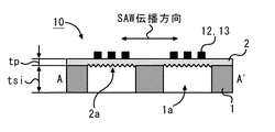
図2に本実施形態による弾性表面波素子10の構造を示す。尚、図2は図3における弾性表面波素子10のA−A’断面の概略図である。但し、本実施形態では、複数の直列共振器(3a)及び複数の並列共振器(3b)がラダー(梯子)型に接続された構成を有するバンドパスフィルタである弾性表面波素子10を例示する。
【0037】
図2において、弾性表面波素子10は、キャビティ(空隙ともいう)1aを有する基板1上に圧電基板2が成膜されており、更に圧電基板2上に櫛形電極(インタデジタルトランスデューサ電極ともいう:以下、IDT電極という)12及び反射電極13が形成された構成を有する。尚、基板1と圧電基板2とは直接接合により接着される。
【0038】
この構成において、圧電基板2は例えばタンタル酸リチウム(LT)やニオブ酸リチウム(LN)で形成される。基板1は圧電基板2より熱膨張率が低い材料(以下、低膨張材料という)であるシリコン(Si)で形成される。このように低膨張材料としてSiを採用することで、本実施形態ではRIE装置を用いて基板1にキャビティ1aを容易に形成することが可能となる。これはキャビティ1aが形成された領域に位置する圧電基板2の裏面に容易に粗面2aを形成できることにも繋がる。
【0039】
圧電基板2の裏面(IDT電極12が形成された面の反対面)におけるキャビティ1aと対応する領域には粗面2aが形成される。これにより、圧電基板2裏面でのバルク波の反射によるフィルタ特性の劣化を防止することが可能となる。但し、この粗面2aを有せず、キャビティ1aのみの構成でも、本実施形態による効果を得ることは可能である。
【0040】
また、キャビティ1aは、例えばIDT電極12と圧電基板2におけるIDT電極12直下の領域とを含んで形成される共振器3に個別に形成される。これにより、必要最低限の面積でキャビティ1aが形成されるため、低膨張材料で形成された基板1の効果を最大限に活用することが可能となる。また、個々のキャビティ1aは、図3に示すように、IDT電極12及びこれの直下に位置する圧電基板2で形成されるIDT4直下の領域だけでなく、反射電極13と圧電基板2における反射電極13直下の領域とで形成される反射器5直下の領域にも延在されるように構成しても良い。換言すれば、キャビティ1aは、1つのIDT電極12と2つの反射電極12とを含んで形成される共振器3の直下の領域に個別に形成されても良い。
【0041】
尚、個々の共振器3が形成される弾性表面波素子10上の位置(又はチップ上の位置ともいう)は、直接接合された基板1の基板厚tsi(図2参照)と圧電基板2の基板厚tp(図2参照)とに基づいて、又は圧電基板2の基板厚tpのみに基づいて決定する。ここで、基板厚tsi及びtpと、弾性表面波(SAW)の伝播方向における弾性表面波素子10の端からの距離d(図3参照)との関係を、図4を用いて説明する。
【0042】
図4はLTを用いた圧電基板2とSiを用いた基板1とを直接接合して形成した弾性表面波素子10に関して、有限要素法を用いて構造解析シミュレーションを行った結果である。この際、圧電基板2の基板厚tpと基板1の基板厚tsiとの比率を変えて、弾性表面波素子10のチップ配置毎の周波数温度特性(Temperature Coefficient of Frequency:以下、TCFという)を計算した。尚、弾性表面波素子10のチップサイズはSAW伝播方向を1.8mmとし、これと垂直な水平方向を1.2mmとした。また、各基板(1,2)の基板厚は図4に示す通りである。このようなチップサイズにおいて、SAW伝播方向に関するチップ端から共振器3までの最短の距離dをパラメータとした。但し、距離dは、弾性表面波素子10の両端に関して何れか最短の方とする。
【0043】
尚、基板1を設けない圧電基板2単体の場合のTCFは約−40ppm/℃である。また、本実施形態において、TCF値が−25ppm/℃程度以下の領域ではTCF値の変動が大きいため、−25ppm/℃以上の領域を有効エリアとする。
【0044】
図4を参照すると、圧電基板2の基板厚tpに依存したTCFの値は、tpが30μmの時、チップ端から100μmで約−25ppm/℃となり、tpが50μmの時、チップ端から200μm弱で約−25ppm/℃となっている。さらに、tpが100μmの時、チップ端から300μmで約−25ppm/℃となっている。また、TCFの値は、基板1の基板厚tsiに若干依存するものの、これを無視することも可能である。
【0045】
従って図4に示すグラフから、良好なTCFが得られるチップ端からの距離dは以下に示す(式1)で表される。尚、この構成は、本実施形態のようなキャビティ1aを有する構成に対してだけでなく、キャビティを有しない弾性表面波素子に対しても有効である。
d≧tp×3 …(式1)
【0046】
以上、説明したように、本実施形態では、熱膨張係数が小さいSi基板を用いることにより、温度変化による伸縮を抑え、電気機械結合係数を低下させること無く、弾性表面波素子の温度安定性を向上することができる。また、基板1にシリコンを用いることにより、RIE装置を用いて容易にキャビティが形成でき、更にキャビティ底面の粗面化を行うことによりバルク波を分散させることが可能となる。このため、バルク波の反射によっておこるリップルやスプリアスを要因とするフィルタ特性の劣化を防止することができる。
【0047】
また、本実施形態では、作製した弾性表面波素子10の共振器3の配置を圧電基板2の基板厚tp(及び基板1の基板厚tsi)に基づいて、チップ端から弾性表面波(SAW)伝播方向において決定するため、基板の剛性による応力を緩和させることなく、温度特性を改善することが可能となる。即ち、本実施形態では、圧電基板の厚みと共振器位置との最適化を行うことにより、周波数変動の少ない弾性表面波素子を実現することができる。また、本実施形態において、圧電基板2はLT基板をLN基板に置き換えたとしても、略同等の結果を得ることができる。また、本実施形態で示す構成を有する弾性表面波素子10は、特にリーキSAW(漏洩弾性表面波)を使用したデバイスに有効である。
【0048】
次に、本実施形態による弾性表面波素子10の製造プロセスについて、図面を用いて詳細に説明する。但し、以下の工程では、300μmのSi基板(基板1)と50μmのLT基板(圧電基板2)とを有する弾性表面波素子10を製造する場合を例に挙げる。
【0049】
図5(a)〜(c)は弾性表面波素子10の製造プロセスを示す断面図である。本製造プロセスでは、まず、(a)に示すように、300μmのSi基板よりなる基板1上に42°YカットX伝播LT基板よりなる圧電基板2を直接接合で接着し、LT基板を50μm程度になるまで研削,研磨する。更に研削,研磨した圧電基板2上に、露光,エッチング等を行うことで、櫛形のIDT電極12及び格子状の反射電極13を形成する。尚、基板1上に圧電基板2を形成する方法には、これらを直接接合とし得るものであれば如何なる方法も適用することが可能である。また、IDT電極12及び反射電極13は、金(Au)やアルミニウム(Al)や銅(Cu)やチタン(Ti)等の少なくとも1つを主成分として形成される。尚、本実施形態では、共振器3がチップ10のSAW伝播方向における端から200μmのところに位置するようにIDT電極12及び反射電極13を形成した。
【0050】
次に、図5(b)に示すように、基板1におけるIDT電極12及び反射電極13が位置する直下の領域を、例えばICP(Inductively Coupled Plasma)エッチング法を用いたディープRIE法(ボッシュプロセス)で、弾性表面波素子10の裏面から除去する。以下の表1に、このボッシュプロセスにおけるエッチング工程とデポジション工程とのパラメータをまとめる。尚、この際、キャビティ1aは、IDT電極12の裏面に位置する領域だけに、可能な限りIDT電極12よりも面積が大きくならないように形成してもよい。
【表1】

図5(b)に示す工程では、上記のパラメータによるエッチング工程とデポジション工程とを例えば250サイクル繰り返すことにより、300μmのSi基板(基板1)を貫通するまでエッチングする。尚、この工程では、ICPエッチング法の他にも、ドライエッチング法やウェットエッチング法やサンドブラスト法等を使用することができる。
【0052】
このように、基板1を圧電基板2が露出されるまでエッチングすると、次に図5(c)に示すように、圧電基板2における露出した領域を、例えばサンドブラスト法を用いて粗面化する。これにより粗面2aが形成される。
【0053】
以上のような工程を経ることで、本実施形態による弾性表面波素子10が形成される。尚、例えば図6に示すようにパッケージ10Aを用いて弾性表面波素子10をパッケージ化することで、これを1つのフィルタ装置として構成することも可能である。この際、パッケージングした内部は、乾燥窒素が充填されるか又は真空にされて密閉される。
【0054】
また、本実施形態において、基板1には例えば1Ω・cm程度以下の比較的低い抵抗率を有するSi基板を使用する。但し、この場合、圧電基板2上に形成された電極パッド6(図3参照)とSi基板(基板1)との間で寄生容量(端子間容量ともいう)が発生する可能性が存在する。本実施形態では、この端子間容量による共振特性の劣化を抑制するために、電極パッド4の面積を可能な限り小さく形成する。これにより、端子間容量の抵抗成分が減少し、共振特性の劣化が抑制されて、比較的低損失な弾性表面波フィルタ、即ちバンドパスフィルタ(又は弾性表面波フィルタ)が実現される。図7に、例として2通りの電極パッド6のサイズ(150μm四方,250μm四方)に関するシミュレーション結果を示す。尚、図7では、弾性表面波素子10における圧電基板2の基板厚を50μmとし、基板1の基板厚を300μmとした。
【0055】
図7を参照すると明らかなように、基板1に比較的低抵抗な材料を使用した場合では、電極パッド6のサイズを小さくした方が減衰量(損失ともいう)が減少し、フィルタ特性が改善することが分かる。
【0056】
〔第2の実施形態〕
次に、本発明の第2の実施形態について図面を用いて詳細に説明する。第1の実施形態では、基板1に比較的低抵抗なSi基板を用いたが、本実施形態では、これを例えば10Ω・cm程度以上の比較的高い抵抗率を有する材料(例えばノンドープのSi)に置き換える。
【0057】
このように、基板1に比較的高抵抗なSi基板を使用することで、本実施形態では、端子間容量のQ値が比較的高い値で構成されるため、共振器の共振抵抗を低く構成することが可能となり、低損失な弾性表面波フィルタが実現される。
【0058】
尚、本実施形態のように、基板1に比較的高抵抗のSi基板を使用する場合、基板1における共振器3(又はIDT電極12)直下の領域にキャビティ1aを形成しなくとも、十分なスプリアス抑制効果を得ることができる。また、他の構成は、第1の実施形態と同様であるため、ここでは説明を省略する。
【0059】
〔第3の実施形態〕
次に、本発明の第3の実施形態について図面を用いて詳細に説明する。図8は本実施形態による弾性表面波素子20の構成を示す断面図である。
【0060】
図8を参照すると明らかなように、弾性表面波素子20は、圧電基板2におけるキャビティ1aが形成された領域に、第1の実施形態のような粗面2aが形成されておらず、この代りにバルク波を吸収するための吸音材7が形成されている。この吸音材7は、例えばエポキシ樹脂等の樹脂が成膜されることで形成される。
【0061】
このような構成を有することにより、本実施形態では、第1の実施形態と同様に、バルク波の反射によっておこるリップルやスプリアスを要因とするフィルタ特性の劣化を防止することができる。また、他の構成は、第1の実施形態と同様であるため、ここでは説明を省略する。
【0062】
〔第4の実施形態〕
次に、本発明の第4の実施形態について図面を用いて詳細に説明する。第1の実施形態では、キャビティ1aを全ての共振器3(又はIDT電極12)の裏面に形成したが、本発明ではこれに限定されず、例えば図9に示す弾性表面波素子30のように、直列共振器3aのみに設けても、また、図10に示す弾性表面波素子40のように、並列共振器3bのみに設けてもよい。換言すれば、本実施形態では、弾性表面波素子10における少なくとも1つの共振器3(又はIDT電極12)にキャビティ1aを設けていればよい。尚、他の構成は、第1の実施形態と同様であるため、ここでは説明を省略する。
【0063】
〔他の実施形態〕
以上、説明した実施形態は本発明の好適な一実施形態にすぎず、本発明はその趣旨を逸脱しない限り種々変形して実施可能である。
【0064】
【発明の効果】
以上説明したように、本発明によれば、熱に対して圧電基板よりも安定で且つ加工が容易なシリコン基板と比較的大きな電気機械結合係数を持つ圧電基板とが直接接合により接合された直接接合基板において、櫛形電極と圧電基板とを有して形成される共振器下の領域にキャビティ(空隙)が形成されるため、フィルタ特性の劣化を生じることなく、比較的大きな電機機械結合係数を持ち且つ温度安定性に優れた、加工が容易な弾性表面波素子が実現される。
【0065】
また、本発明によれば、熱に対して圧電基板よりも安定で且つ加工が容易なシリコン基板と比較的大きな電気機械結合係数を持つ圧電基板とが直接接合により接合された直接接合基板において、圧電基板の基板厚に応じて共振器の弾性表面波伝播方向における素子端からの距離を確保することで、温度安定性が十分に得られる。
【0066】
また、本発明によれば、上記の効果を得られる弾性表面波素子をパッケージ化したフィルタ装置として提供することができる。更に、本発明によれば、上記の効果を得られる弾性表面波素子の製造方法が提供される。
【図面の簡単な説明】
【図1】従来技術による弾性表面波素子の構成を示す断面図であり、(a)は従来技術1による弾性表面波素子100の構成を示し、(b)は従来技術2による弾性表面波素子200の構成を示し、(c)は従来技術3による弾性表面波素子300の構成を示し、(d)は従来技術4による弾性表面波素子400の構成を示す。
【図2】本発明の第1の実施形態による弾性表面波素子10の概略構成を示す断面図である。
【図3】図2に示す弾性表面波素子10の構成を示す上面図である。
【図4】基板厚tsi及びtpと弾性表面波(SAW)の伝播方向における弾性表面波素子10の端からの距離dとの関係を示すグラフである。
【図5】本発明の第1の実施形態による弾性表面波素子10の製造プロセスを示す断面図である。
【図6】弾性表面波素子10をパッケージ化した構成を示す断面図である。
【図7】本発明の第1の実施形態による弾性表面波素子10において2通りの電極パッド4のサイズ(150μm四方,250μm四方)に関するシミュレーション結果を示すグラフである。
【図8】本発明の第3の実施形態による弾性表面波素子20の構成を示す断面図である。
【図9】本発明の第4の実施形態による弾性表面波素子30の構成を示す上面図である。
【図10】本発明の第4の実施形態による弾性表面波素子40の構成を示す上面図である。
【符号の説明】
1 基板
1a キャビティ
2 圧電基板
2a 粗面
3 共振器
3a 直列共振器
3b 並列共振器
4 IDT
5 反射器
6 電極パッド
7 吸音材
10、20、30、40 弾性表面波素子
10A パッケージ
12 櫛形(IDT)電極
13 反射電極[0001]
BACKGROUND OF THE INVENTION
The present invention relates to a surface acoustic wave element, a filter device, and a manufacturing method thereof using a piezoelectric substrate and a low expansion material.
[0002]
[Prior art]
Currently, surface acoustic wave devices are widely used as bandpass filters for mobile phones. Filters and resonators using this surface acoustic wave element are characterized in that they are small and inexpensive. Therefore, surface acoustic wave elements are indispensable for miniaturization of communication devices such as mobile phones.
[0003]
In recent years, with the improvement in performance of mobile phones and the like, further improvement in performance is also required for filters using surface acoustic wave elements. However, since the surface acoustic wave element fluctuates in frequency due to a temperature change, improvement in temperature stability is required.
[0004]
In the prior art, lithium tantalate (hereinafter referred to as LT), which is frequently used as a substrate material for surface acoustic wave elements, is a piezoelectric material having a large electromechanical coupling coefficient.
[0005]
As a general tendency of piezoelectric materials, a material having a large electromechanical coupling coefficient is inferior in temperature stability, and conversely, a material such as quartz having excellent temperature stability has a small electromechanical coupling coefficient. For this reason, the surface acoustic wave element using the LT substrate is advantageous for realizing a wide-band filter characteristic, but has a defect that the temperature stability is inferior to that of a quartz substrate or the like.
[0006]
Conventionally, various methods have been proposed in order to compensate for such drawbacks and realize a material having a large electromechanical coupling coefficient and excellent temperature stability. FIG. 1 shows some conventional temperature characteristic improving techniques.
[0007]
FIG. 1A is a cross-sectional view showing a configuration of a conventional surface acoustic wave element 100 (see, for example, Non-Patent Document 1). This is hereinafter referred to as Prior Art 1. The surface
[0008]
FIG. 1B is a cross-sectional view showing a configuration of a conventional surface acoustic wave element 200 (see, for example, Patent Document 1). This is hereinafter referred to as Prior Art 2. The surface
[0009]
FIG. 1C is a cross-sectional view showing the configuration of a conventional surface acoustic wave element 300 (see, for example,
[0010]
However, in the above-described conventional technology, it is difficult to control the quality of the
[0011]
Further, the surface
[0012]
To solve this problem, the back surface of the
[0013]
[Patent Document 1]
Japanese Patent No. 2516817
[Patent Document 2]
Japanese Patent Laid-Open No. 11-55070
[Patent Document 3]
JP 2001-53579 A
[Non-Patent Document 1]
Yamanouchi et al., IEEE Trans. on Sonics and Ultrasonics. , Vol. SU-31, pp. 51-57 (1984)
[Non-Patent Document 2]
Onishi et al., Proc. of IEEE Ultrasonics Symposium, pp. 335-338 (1998)
[0014]
[Problems to be solved by the invention]
However, although the prior art 4 can improve the filter characteristics, since the adhesive layer 17 is provided at the bonding interface between the
[0015]
The present invention has been made in view of the above problems, and has a relatively large electromechanical coupling coefficient and excellent temperature stability without causing deterioration of filter characteristics, and an easily processed surface acoustic wave device, An object of the present invention is to provide a filter device and a manufacturing method thereof.
[0016]
[Means for Solving the Problems]
To achieve this object, the present invention includes a comb electrode as claimed in claim 1.pluralA surface acoustic wave device in which a piezoelectric substrate having a resonator and a silicon substrate having a lower expansion than the piezoelectric substrate are directly bonded, and the region of the silicon substrate under each resonator is defined for each of the plurality of resonators. The penetrating cavityIndividuallyIt has the structure formed. As a result, in a direct bonding substrate in which a silicon substrate that is more stable and easier to process than heat and easily processed, and a piezoelectric substrate having a relatively large electromechanical coupling coefficient are bonded by direct bonding, the comb electrode and the piezoelectric substrate Since a cavity (gap) is formed in a region under the resonator formed by having a relatively large electromechanical coupling coefficient and excellent temperature stability without causing deterioration of filter characteristics, A surface acoustic wave element that can be easily processed is realized.
[0017]
Further, the surface acoustic wave element is, for example, as described in
[0018]
Further, the surface acoustic wave element is, for example, as described in
[0019]
In addition, the surface acoustic wave element may be configured such that a region exposed by the cavity in the piezoelectric substrate is roughened, for example. As a result, it is possible to prevent the bulk wave from being reflected on the surface of the piezoelectric substrate opposite to the surface on which the comb-shaped electrodes are formed, and thus it is possible to prevent the deterioration of the filter characteristics.
[0020]
As another example, the surface acoustic wave element may be configured to have a sound absorbing film on a region exposed by the cavity in the piezoelectric substrate, for example. As a result, it is possible to prevent the bulk wave from being reflected on the surface of the piezoelectric substrate opposite to the surface on which the comb-shaped electrodes are formed, and thus it is possible to prevent the deterioration of the filter characteristics.
[0021]
Further, the surface acoustic wave element is, for example, as described in claim 6,The surface acoustic wave element may further include a resonator, and a structure under the resonator may be a region of a silicon substrate where no cavity exists.
[0022]
In addition, the surface acoustic wave element may be configured such that the piezoelectric substrate is formed of lithium tantalate or lithium niobate, as described in
[0023]
Further, the present invention provides the following, as described in claim 8.AboveThe silicon substrate has a resistivity of 10 Ω · cm or more. Thus, energy loss can be reduced by using a relatively high resistance silicon substrate having a resistivity of 10 Ω · cm or more.
[0024]
Further, the present invention provides the following, as described in claim 9.AboveThe resonator is configured such that the distance d from the element end in the direction in which the surface acoustic wave propagates is formed at a position satisfying the following formula 1 where the thickness of the piezoelectric substrate is tp. Thus, in the direct bonding substrate in which the substrate that is more stable and easier to process than the piezoelectric substrate and that has a relatively large electromechanical coupling coefficient is bonded by direct bonding, the substrate thickness of the piezoelectric substrate is reduced. Accordingly, the temperature stability is sufficiently obtained by securing the distance from the element end in the surface acoustic wave propagation direction of the resonator.
d ≧ tp × 3 (Formula 1)
[0025]
According to a tenth aspect of the present invention, there is provided a configuration comprising any one of the surface acoustic wave elements described above and an electrode pad formed on the piezoelectric substrate for introducing an electric signal into the comb-shaped electrode. And Thereby, it is possible to provide a surface acoustic wave element that can obtain the above-described effect as a packaged filter device.
[0026]
Further, the present invention includes a comb electrode as described in claim 11.pluralA manufacturing method for manufacturing a surface acoustic wave device in which a piezoelectric substrate having a resonator and a silicon substrate having a lower expansion than the piezoelectric substrate are directly bonded, wherein the silicon under each resonator is provided for each of the plurality of resonators. A cavity that penetrates the area of the substrateIndividuallyThe first step is formed. Accordingly, a comb-shaped electrode and a piezoelectric substrate in a direct bonding substrate in which a silicon substrate that is more stable and easier to process than a piezoelectric substrate and a piezoelectric substrate having a relatively large electromechanical coupling coefficient are bonded by direct bonding. A cavity (air gap) can be formed in the region under the resonator formed with the elastic surface, having a relatively large electromechanical coupling coefficient and excellent temperature stability without causing deterioration of the filter characteristics A wave element can be manufactured easily.
[0027]
Moreover, said manufacturing method is the said, for example like Claim 12.pluralThe resonatorRespectivelyA reflective electrode adjacent to the comb-shaped electrode may be included, and the first step may be configured to form the cavity also in a region under the reflective electrode in the silicon substrate. As a result, it is possible to realize a configuration that avoids deterioration of the reflection characteristics of the reflector formed by the reflective electrode and the piezoelectric substrate, and as a result, it is possible to manufacture a surface acoustic wave element in which deterioration of the filter characteristics is prevented.
[0028]
In addition, the manufacturing method described above may be configured to include a second step of roughening a region exposed by the cavity in the piezoelectric substrate, for example. This realizes a configuration that prevents bulk waves from being reflected from the surface opposite to the surface on which the comb-shaped electrodes are formed on the piezoelectric substrate. As a result, the surface acoustic wave device that prevents deterioration in filter characteristics can be obtained. Can be manufactured.
[0029]
As another example, the manufacturing method includes a second step of forming a sound-absorbing film on a region exposed by the cavity in the piezoelectric substrate, for example, as in
[0030]
Further, the above manufacturing method is, for example, as described in
[0031]
Further, in the above manufacturing method, for example, as in
[0032]
In addition, the above manufacturing method may be configured such that the piezoelectric substrate is made of lithium tantalate or lithium niobate, for example. Thus, in the present invention, it is possible to use general lithium tantalate or lithium niobate as the material of the piezoelectric substrate.
[0033]
Further, the above manufacturing method is, for example, as described in claim 19,AboveIn the first step, the resonator is formed at a position where the distance d from the element end in the direction in which the surface acoustic wave propagates satisfies the following formula 1 where the thickness of the piezoelectric substrate is tp. Thus, in the direct bonding substrate in which the substrate that is more stable and easier to process than the piezoelectric substrate and that has a relatively large electromechanical coupling coefficient is bonded by direct bonding, the substrate thickness of the piezoelectric substrate is reduced. Accordingly, the temperature stability is sufficiently obtained by securing the distance from the element end in the surface acoustic wave propagation direction of the resonator.
d ≧ tp × 3 (Formula 1)
[0034]
DETAILED DESCRIPTION OF THE INVENTION
DESCRIPTION OF EMBODIMENTS Hereinafter, preferred embodiments of the present invention will be described in detail with reference to the drawings.
[0035]
[First Embodiment]
First, a first embodiment of the present invention will be described in detail with reference to the drawings. In the present embodiment, a cavity is formed using a RIE (reactive ion etching) apparatus in a direct bonding substrate in which a piezoelectric substrate and a low expansion material (silicon substrate) having a small thermal expansion coefficient are integrated by direct bonding. By roughening the bottom surface, a surface acoustic wave element having a large electromechanical coupling coefficient and excellent temperature stability and easy to process without causing deterioration of filter characteristics is realized.
[0036]
FIG. 2 shows the structure of the surface
[0037]
In FIG. 2, a surface
[0038]
In this configuration, the
[0039]
A
[0040]
Further, the
[0041]
The position on the surface
[0042]
FIG. 4 shows the result of structural analysis simulation using the finite element method for the surface
[0043]
Note that the TCF in the case of the
[0044]
Referring to FIG. 4, the value of TCF depending on the substrate thickness tp of the
[0045]
Therefore, from the graph shown in FIG. 4, the distance d from the chip end at which a good TCF is obtained is expressed by the following (formula 1). This configuration is effective not only for the configuration having the
d ≧ tp × 3 (Formula 1)
[0046]
As described above, in this embodiment, by using a Si substrate having a small thermal expansion coefficient, the temperature stability of the surface acoustic wave element can be improved without suppressing expansion and contraction due to temperature change and reducing the electromechanical coupling coefficient. Can be improved. Further, by using silicon for the substrate 1, a cavity can be easily formed by using an RIE apparatus, and bulk waves can be dispersed by roughening the bottom surface of the cavity. For this reason, it is possible to prevent deterioration of filter characteristics caused by ripples and spurious caused by reflection of bulk waves.
[0047]
In the present embodiment, the arrangement of the
[0048]
Next, the manufacturing process of the surface
[0049]
5A to 5C are cross-sectional views showing a manufacturing process of the surface
[0050]
Next, as shown in FIG. 5B, a deep RIE method (Bosch process) using, for example, an ICP (Inductively Coupled Plasma) etching method is performed on the region immediately below the
[Table 1]
In the process shown in FIG. 5B, the etching process and the deposition process using the above parameters are repeated, for example, 250 cycles, thereby performing etching until the 300 μm Si substrate (substrate 1) is penetrated. In this step, in addition to the ICP etching method, a dry etching method, a wet etching method, a sand blasting method, or the like can be used.
[0052]
When the substrate 1 is thus etched until the
[0053]
Through the above steps, the surface
[0054]
In the present embodiment, a Si substrate having a relatively low resistivity of, for example, about 1 Ω · cm or less is used as the substrate 1. However, in this case, there is a possibility that parasitic capacitance (also referred to as inter-terminal capacitance) is generated between the electrode pad 6 (see FIG. 3) formed on the
[0055]
As apparent from FIG. 7, when a relatively low resistance material is used for the substrate 1, the electrode pad6If the size of the filter is reduced, the amount of attenuation (also called loss) decreases, and the filter characteristicsImproveI understand that.
[0056]
[Second Embodiment]
Next, a second embodiment of the present invention will be described in detail with reference to the drawings. In the first embodiment, a Si substrate having a relatively low resistance is used as the substrate 1, but in the present embodiment, this is a material having a relatively high resistivity of, for example, about 10 Ω · cm or more (for example, non-doped Si). Replace with
[0057]
As described above, by using a relatively high resistance Si substrate for the substrate 1, in this embodiment, the Q value of the inter-terminal capacitance is configured to be a relatively high value, so that the resonance resistance of the resonator is configured to be low. Therefore, a low-loss surface acoustic wave filter can be realized.
[0058]
When a relatively high resistance Si substrate is used as the substrate 1 as in the present embodiment, it is sufficient even if the
[0059]
[Third Embodiment]
Next, a third embodiment of the present invention will be described in detail with reference to the drawings. FIG. 8 is a cross-sectional view showing the configuration of the surface
[0060]
As apparent from FIG. 8, the surface
[0061]
By having such a configuration, in this embodiment, as in the first embodiment, it is possible to prevent deterioration of filter characteristics due to ripples and spurious caused by reflection of bulk waves. Other configurations are the same as those of the first embodiment, and thus description thereof is omitted here.
[0062]
[Fourth Embodiment]
Next, a fourth embodiment of the present invention will be described in detail with reference to the drawings. In the first embodiment, the
[0063]
[Other Embodiments]
The embodiment described above is merely a preferred embodiment of the present invention, and the present invention can be variously modified and implemented without departing from the gist thereof.
[0064]
【The invention's effect】
As described above, according to the present invention, a silicon substrate that is more stable and easier to process than a piezoelectric substrate with respect to heat and a piezoelectric substrate having a relatively large electromechanical coupling coefficient are directly bonded. In the bonded substrate, a cavity (gap) is formed in a region under the resonator formed by having the comb-shaped electrode and the piezoelectric substrate, so that a relatively large electromechanical coupling coefficient can be obtained without causing deterioration of the filter characteristics. A surface acoustic wave element that is easy to process and has excellent temperature stability is realized.
[0065]
Further, according to the present invention, in a direct bonding substrate in which a silicon substrate that is more stable and easy to process than a piezoelectric substrate with respect to heat and a piezoelectric substrate having a relatively large electromechanical coupling coefficient are bonded by direct bonding, By ensuring the distance from the element end in the surface acoustic wave propagation direction of the resonator according to the substrate thickness of the piezoelectric substrate, sufficient temperature stability can be obtained.
[0066]
In addition, according to the present invention, it is possible to provide a filter device in which a surface acoustic wave element capable of obtaining the above-described effect is packaged. Furthermore, according to this invention, the manufacturing method of the surface acoustic wave element which can acquire said effect is provided.
[Brief description of the drawings]
1A and 1B are cross-sectional views showing a configuration of a surface acoustic wave element according to the prior art, FIG. 1A shows a configuration of a surface
FIG. 2 is a cross-sectional view showing a schematic configuration of the surface
3 is a top view showing a configuration of the surface
FIG. 4 is a graph showing a relationship between substrate thicknesses tsi and tp and a distance d from the end of the surface
FIG. 5 is a cross-sectional view showing a manufacturing process of the surface
6 is a cross-sectional view showing a configuration in which a surface
7 is a graph showing simulation results regarding the sizes (150 μm square and 250 μm square) of two electrode pads 4 in the surface
FIG. 8 is a cross-sectional view showing a configuration of a surface
FIG. 9 is a top view showing a configuration of a surface
FIG. 10 is a top view showing a configuration of a surface
[Explanation of symbols]
1 Substrate
1a cavity
2 Piezoelectric substrate
2a Rough surface
3 Resonator
3a Series resonator
3b Parallel resonator
4 IDT
5 reflectors
6 Electrode pads
7 Sound absorbing material
10, 20, 30, 40 Surface acoustic wave device
10A package
12 Comb (IDT) electrode
13 Reflective electrode
Claims (19)
前記複数の共振器ごとに、各共振器下の前記シリコン基板の領域を貫通するキャビティが個別に形成されていることを特徴とする弾性表面波素子。A surface acoustic wave device in which a piezoelectric substrate having a plurality of resonators including comb-shaped electrodes and a silicon substrate having a lower expansion than the piezoelectric substrate are directly bonded,
A surface acoustic wave device, wherein a cavity penetrating a region of the silicon substrate under each resonator is individually formed for each of the plurality of resonators.
前記キャビティは前記シリコン基板における前記反射電極下の領域にも形成されていることを特徴とする請求項1記載の弾性表面波素子。Each of the plurality of resonators includes a reflective electrode adjacent to the comb electrode;
2. The surface acoustic wave device according to claim 1, wherein the cavity is also formed in a region under the reflective electrode in the silicon substrate.
前記キャビティは前記シリコン基板における前記櫛形電極下の領域のみに形成されていることを特徴とする請求項1記載の弾性表面波素子。Each of the plurality of resonators includes a reflective electrode adjacent to the comb electrode;
2. The surface acoustic wave device according to claim 1, wherein the cavity is formed only in a region under the comb electrode on the silicon substrate.
d≧tp×3 …(式1)9. The resonator according to claim 1, wherein a distance d from the element end in a direction in which the surface acoustic wave propagates is formed at a position satisfying the following expression 1 where the thickness of the piezoelectric substrate is tp. The surface acoustic wave element according to claim 1.
d ≧ tp × 3 (Formula 1)
前記複数の共振器ごとに、各共振器下の前記シリコン基板の領域を貫通するキャビティを個別に形成する第1の工程を有することを特徴とする弾性表面波素子の製造方法。A manufacturing method for manufacturing a surface acoustic wave device in which a piezoelectric substrate having a plurality of resonators including comb-shaped electrodes and a silicon substrate having a lower expansion than the piezoelectric substrate are directly bonded,
A method of manufacturing a surface acoustic wave device, comprising: a first step of individually forming a cavity penetrating a region of the silicon substrate under each resonator for each of the plurality of resonators.
前記第1の工程は前記シリコン基板における前記反射電極下の領域にも前記キャビティを形成することを特徴とする請求項11記載の弾性表面波素子の製造方法。Each of the plurality of resonators includes a reflective electrode adjacent to the comb electrode;
12. The method of manufacturing a surface acoustic wave device according to claim 11, wherein the first step forms the cavity also in a region under the reflective electrode in the silicon substrate.
前記第1の工程は、前記櫛形電極下の領域のみに前記キャビティを形成することを特徴とする請求項11、13又は14の何れか1項に記載の弾性表面波素子の製造方法。Each of the plurality of resonators includes a reflective electrode adjacent to the comb electrode;
The method for manufacturing a surface acoustic wave device according to claim 11, wherein the first step forms the cavity only in a region under the comb-shaped electrode.
d≧tp×3 …(式1)The first step is characterized in that the resonator is formed at a position where the distance d from the element end in the direction in which the surface acoustic wave propagates satisfies the following formula 1 where the thickness of the piezoelectric substrate is tp. Item 19. A method for manufacturing a surface acoustic wave device according to any one of Items 11 to 18.
d ≧ tp × 3 (Formula 1)
Priority Applications (4)
| Application Number | Priority Date | Filing Date | Title |
|---|---|---|---|
| JP2002258642A JP3892370B2 (en) | 2002-09-04 | 2002-09-04 | Surface acoustic wave element, filter device, and manufacturing method thereof |
| US10/653,213 US7067956B2 (en) | 2002-09-04 | 2003-09-03 | Surface acoustic wave device, filter device and method of producing the surface acoustic wave device |
| KR1020030061378A KR100625718B1 (en) | 2002-09-04 | 2003-09-03 | Surface acoustic wave device, filter device and method of producing the surface acoustic wave device |
| CNA031562183A CN1489285A (en) | 2002-09-04 | 2003-09-04 | Surface acoustic wave device, filter device and method of manufacturing surface acoustic wave device |
Applications Claiming Priority (1)
| Application Number | Priority Date | Filing Date | Title |
|---|---|---|---|
| JP2002258642A JP3892370B2 (en) | 2002-09-04 | 2002-09-04 | Surface acoustic wave element, filter device, and manufacturing method thereof |
Publications (2)
| Publication Number | Publication Date |
|---|---|
| JP2004096677A JP2004096677A (en) | 2004-03-25 |
| JP3892370B2 true JP3892370B2 (en) | 2007-03-14 |
Family
ID=31973033
Family Applications (1)
| Application Number | Title | Priority Date | Filing Date |
|---|---|---|---|
| JP2002258642A Expired - Fee Related JP3892370B2 (en) | 2002-09-04 | 2002-09-04 | Surface acoustic wave element, filter device, and manufacturing method thereof |
Country Status (4)
| Country | Link |
|---|---|
| US (1) | US7067956B2 (en) |
| JP (1) | JP3892370B2 (en) |
| KR (1) | KR100625718B1 (en) |
| CN (1) | CN1489285A (en) |
Families Citing this family (115)
| Publication number | Priority date | Publication date | Assignee | Title |
|---|---|---|---|---|
| CN1938946A (en) * | 2004-03-29 | 2007-03-28 | 株式会社村田制作所 | Boundary acoustic wave device manufacturing method and boundary acoustic wave device |
| JP4723207B2 (en) * | 2004-05-31 | 2011-07-13 | 信越化学工業株式会社 | Composite piezoelectric substrate |
| JP2006025396A (en) | 2004-06-09 | 2006-01-26 | Seiko Epson Corp | Surface acoustic wave device, manufacturing method thereof, and electronic apparatus |
| US7307369B2 (en) * | 2004-08-26 | 2007-12-11 | Kyocera Corporation | Surface acoustic wave device, surface acoustic wave apparatus, and communications equipment |
| JP2007243918A (en) * | 2006-02-08 | 2007-09-20 | Seiko Epson Corp | Surface acoustic wave device and electronic device |
| JP4315174B2 (en) * | 2006-02-16 | 2009-08-19 | セイコーエプソン株式会社 | Manufacturing method of lamb wave type high frequency device |
| US7569976B2 (en) * | 2006-07-27 | 2009-08-04 | Koike Co., Ltd. | Piezo-electric substrate and manufacturing method of the same |
| JP2008135999A (en) * | 2006-11-28 | 2008-06-12 | Fujitsu Media Device Kk | Elastic wave device and manufacturing method thereof |
| DE102007037502B4 (en) * | 2007-08-08 | 2014-04-03 | Epcos Ag | Component with reduced temperature response |
| EP2237417B1 (en) * | 2008-01-25 | 2013-07-31 | Murata Manufacturing Co. Ltd. | Elastic wave element and method for manufacturing the same |
| JP4863097B2 (en) * | 2009-08-11 | 2012-01-25 | 株式会社村田製作所 | Manufacturing method of surface acoustic wave device |
| JP5301413B2 (en) * | 2009-10-22 | 2013-09-25 | 日本碍子株式会社 | Manufacturing method of composite substrate |
| JP5333538B2 (en) * | 2011-07-27 | 2013-11-06 | 株式会社デンソー | Surface acoustic wave sensor |
| US9893264B2 (en) * | 2012-06-15 | 2018-02-13 | Carnegie Mellon University | Method for forming a suspended lithium-based membrane semiconductor structure |
| DE102013215246A1 (en) * | 2013-08-02 | 2015-02-05 | Robert Bosch Gmbh | Electronic module with printed circuit boards and injection-molded plastic sealing ring, in particular for a motor vehicle transmission control unit, and method for manufacturing the same |
| US10541152B2 (en) | 2014-07-31 | 2020-01-21 | Skyworks Solutions, Inc. | Transient liquid phase material bonding and sealing structures and methods of forming same |
| CN105448869A (en) | 2014-07-31 | 2016-03-30 | 天工方案公司 | Multilayered transient liquid phase bonding |
| US10177734B2 (en) | 2015-08-25 | 2019-01-08 | Avago Technologies International Sales Pte. Limited | Surface acoustic wave (SAW) resonator |
| US10536133B2 (en) | 2016-04-22 | 2020-01-14 | Avago Technologies International Sales Pte. Limited | Composite surface acoustic wave (SAW) device with absorbing layer for suppression of spurious responses |
| US10020796B2 (en) | 2015-08-25 | 2018-07-10 | Avago Technologies General Ip (Singapore) Pte. Ltd. | Surface acoustic wave (SAW) resonator |
| DE102015120341A1 (en) * | 2015-11-24 | 2017-05-24 | Snaptrack, Inc. | Component with heat dissipation |
| US10177735B2 (en) | 2016-02-29 | 2019-01-08 | Avago Technologies International Sales Pte. Limited | Surface acoustic wave (SAW) resonator |
| US10715105B2 (en) * | 2016-06-24 | 2020-07-14 | Murata Manufacturing Co., Ltd. | Acoustic wave device |
| FR3053532B1 (en) * | 2016-06-30 | 2018-11-16 | Soitec | HYBRID STRUCTURE FOR ACOUSTIC SURFACE WAVE DEVICE |
| JP2018037719A (en) * | 2016-08-29 | 2018-03-08 | 株式会社村田製作所 | Acoustic wave device |
| US20180159502A1 (en) | 2016-12-02 | 2018-06-07 | Skyworks Solutions, Inc. | Methods of manufacturing electronic devices to prevent water ingress during manufacture |
| CN106961258B (en) * | 2017-05-04 | 2023-08-15 | 杭州左蓝微电子技术有限公司 | Cavity type surface acoustic wave resonator and processing method thereof |
| WO2019111893A1 (en) * | 2017-12-06 | 2019-06-13 | 株式会社村田製作所 | Acoustic wave device |
| US11323096B2 (en) | 2018-06-15 | 2022-05-03 | Resonant Inc. | Transversely-excited film bulk acoustic resonator with periodic etched holes |
| US11929731B2 (en) | 2018-02-18 | 2024-03-12 | Murata Manufacturing Co., Ltd. | Transversely-excited film bulk acoustic resonator with optimized electrode mark, and pitch |
| US11936358B2 (en) | 2020-11-11 | 2024-03-19 | Murata Manufacturing Co., Ltd. | Transversely-excited film bulk acoustic resonator with low thermal impedance |
| US10637438B2 (en) | 2018-06-15 | 2020-04-28 | Resonant Inc. | Transversely-excited film bulk acoustic resonators for high power applications |
| US11509279B2 (en) | 2020-07-18 | 2022-11-22 | Resonant Inc. | Acoustic resonators and filters with reduced temperature coefficient of frequency |
| US11206009B2 (en) | 2019-08-28 | 2021-12-21 | Resonant Inc. | Transversely-excited film bulk acoustic resonator with interdigital transducer with varied mark and pitch |
| US10911023B2 (en) | 2018-06-15 | 2021-02-02 | Resonant Inc. | Transversely-excited film bulk acoustic resonator with etch-stop layer |
| US11323090B2 (en) | 2018-06-15 | 2022-05-03 | Resonant Inc. | Transversely-excited film bulk acoustic resonator using Y-X-cut lithium niobate for high power applications |
| US11323089B2 (en) | 2018-06-15 | 2022-05-03 | Resonant Inc. | Filter using piezoelectric film bonded to high resistivity silicon substrate with trap-rich layer |
| US11996827B2 (en) | 2018-06-15 | 2024-05-28 | Murata Manufacturing Co., Ltd. | Transversely-excited film bulk acoustic resonator with periodic etched holes |
| US10491192B1 (en) * | 2018-06-15 | 2019-11-26 | Resonant Inc. | Transversely-excited film bulk acoustic resonator |
| US12040779B2 (en) | 2020-04-20 | 2024-07-16 | Murata Manufacturing Co., Ltd. | Small transversely-excited film bulk acoustic resonators with enhanced Q-factor |
| US12088281B2 (en) | 2021-02-03 | 2024-09-10 | Murata Manufacturing Co., Ltd. | Transversely-excited film bulk acoustic resonator with multi-mark interdigital transducer |
| US11146232B2 (en) | 2018-06-15 | 2021-10-12 | Resonant Inc. | Transversely-excited film bulk acoustic resonator with reduced spurious modes |
| US12237826B2 (en) | 2018-06-15 | 2025-02-25 | Murata Manufacturing Co., Ltd. | Transversely-excited film bulk acoustic resonator with optimized electrode thickness, mark, and pitch |
| US10601392B2 (en) | 2018-06-15 | 2020-03-24 | Resonant Inc. | Solidly-mounted transversely-excited film bulk acoustic resonator |
| US10992284B2 (en) | 2018-06-15 | 2021-04-27 | Resonant Inc. | Filter using transversely-excited film bulk acoustic resonators with multiple frequency setting layers |
| US11264966B2 (en) | 2018-06-15 | 2022-03-01 | Resonant Inc. | Solidly-mounted transversely-excited film bulk acoustic resonator with diamond layers in Bragg reflector stack |
| US12155374B2 (en) | 2021-04-02 | 2024-11-26 | Murata Manufacturing Co., Ltd. | Tiled transversely-excited film bulk acoustic resonator high power filters |
| US12095441B2 (en) | 2018-06-15 | 2024-09-17 | Murata Manufacturing Co., Ltd. | Transversely excited film bulk acoustic resonator with recessed interdigital transducer fingers |
| US12184261B2 (en) | 2018-06-15 | 2024-12-31 | Murata Manufacturing Co., Ltd. | Transversely-excited film bulk acoustic resonator with a cavity having round end zones |
| US11996822B2 (en) | 2018-06-15 | 2024-05-28 | Murata Manufacturing Co., Ltd. | Wide bandwidth time division duplex transceiver |
| US12119808B2 (en) | 2018-06-15 | 2024-10-15 | Murata Manufacturing Co., Ltd. | Transversely-excited film bulk acoustic resonator package |
| US11967945B2 (en) | 2018-06-15 | 2024-04-23 | Murata Manufacturing Co., Ltd. | Transversly-excited film bulk acoustic resonators and filters |
| US12040781B2 (en) | 2018-06-15 | 2024-07-16 | Murata Manufacturing Co., Ltd. | Transversely-excited film bulk acoustic resonator package |
| US12149227B2 (en) | 2018-06-15 | 2024-11-19 | Murata Manufacturing Co., Ltd. | Transversely-excited film bulk acoustic resonator package |
| US12212306B2 (en) | 2018-06-15 | 2025-01-28 | Murata Manufacturing Co., Ltd. | Transversely-excited film bulk acoustic resonator with multiple diaphragm thicknesses and fabrication method |
| US12191837B2 (en) | 2018-06-15 | 2025-01-07 | Murata Manufacturing Co., Ltd. | Solidly-mounted transversely-excited film bulk acoustic device |
| US11870423B2 (en) | 2018-06-15 | 2024-01-09 | Murata Manufacturing Co., Ltd. | Wide bandwidth temperature-compensated transversely-excited film bulk acoustic resonator |
| US11146238B2 (en) | 2018-06-15 | 2021-10-12 | Resonant Inc. | Film bulk acoustic resonator fabrication method |
| US12095446B2 (en) | 2018-06-15 | 2024-09-17 | Murata Manufacturing Co., Ltd. | Transversely-excited film bulk acoustic resonator with optimized electrode thickness, mark, and pitch |
| US11901878B2 (en) | 2018-06-15 | 2024-02-13 | Murata Manufacturing Co., Ltd. | Transversely-excited film bulk acoustic resonators with two-layer electrodes with a wider top layer |
| US12021496B2 (en) | 2020-08-31 | 2024-06-25 | Murata Manufacturing Co., Ltd. | Resonators with different membrane thicknesses on the same die |
| US11909381B2 (en) | 2018-06-15 | 2024-02-20 | Murata Manufacturing Co., Ltd. | Transversely-excited film bulk acoustic resonators with two-layer electrodes having a narrower top layer |
| US10917072B2 (en) | 2019-06-24 | 2021-02-09 | Resonant Inc. | Split ladder acoustic wave filters |
| US11888463B2 (en) | 2018-06-15 | 2024-01-30 | Murata Manufacturing Co., Ltd. | Multi-port filter using transversely-excited film bulk acoustic resonators |
| US10819309B1 (en) | 2019-04-05 | 2020-10-27 | Resonant Inc. | Transversely-excited film bulk acoustic resonator package and method |
| US12191838B2 (en) | 2018-06-15 | 2025-01-07 | Murata Manufacturing Co., Ltd. | Solidly-mounted transversely-excited film bulk acoustic device and method |
| US11996825B2 (en) | 2020-06-17 | 2024-05-28 | Murata Manufacturing Co., Ltd. | Filter using lithium niobate and rotated lithium tantalate transversely-excited film bulk acoustic resonators |
| US11323091B2 (en) | 2018-06-15 | 2022-05-03 | Resonant Inc. | Transversely-excited film bulk acoustic resonator with diaphragm support pedestals |
| US12224732B2 (en) | 2018-06-15 | 2025-02-11 | Murata Manufacturing Co., Ltd. | Solidly-mounted transversely-excited film bulk acoustic resonators and filters for 27 GHz communications bands |
| US10998882B2 (en) | 2018-06-15 | 2021-05-04 | Resonant Inc. | XBAR resonators with non-rectangular diaphragms |
| US11876498B2 (en) | 2018-06-15 | 2024-01-16 | Murata Manufacturing Co., Ltd. | Transversely-excited film bulk acoustic resonator with multiple diaphragm thicknesses and fabrication method |
| US12009798B2 (en) | 2018-06-15 | 2024-06-11 | Murata Manufacturing Co., Ltd. | Transversely-excited film bulk acoustic resonators with electrodes having irregular hexagon cross-sectional shapes |
| US12237827B2 (en) | 2018-06-15 | 2025-02-25 | Murata Manufacturing Co., Ltd. | Solidly-mounted transversely-excited film bulk acoustic filters with multiple piezoelectric plate thicknesses |
| US10826462B2 (en) | 2018-06-15 | 2020-11-03 | Resonant Inc. | Transversely-excited film bulk acoustic resonators with molybdenum conductors |
| US11916539B2 (en) | 2020-02-28 | 2024-02-27 | Murata Manufacturing Co., Ltd. | Split-ladder band N77 filter using transversely-excited film bulk acoustic resonators |
| US10985728B2 (en) | 2018-06-15 | 2021-04-20 | Resonant Inc. | Transversely-excited film bulk acoustic resonator and filter with a uniform-thickness dielectric overlayer |
| US12155371B2 (en) | 2021-03-29 | 2024-11-26 | Murata Manufacturing Co., Ltd. | Layout of xbars with multiple sub-resonators in series |
| US11349452B2 (en) | 2018-06-15 | 2022-05-31 | Resonant Inc. | Transversely-excited film bulk acoustic filters with symmetric layout |
| US11374549B2 (en) | 2018-06-15 | 2022-06-28 | Resonant Inc. | Filter using transversely-excited film bulk acoustic resonators with divided frequency-setting dielectric layers |
| US12081187B2 (en) | 2018-06-15 | 2024-09-03 | Murata Manufacturing Co., Ltd. | Transversely-excited film bulk acoustic resonator |
| US12132464B2 (en) | 2018-06-15 | 2024-10-29 | Murata Manufacturing Co., Ltd. | Filter using transversely-excited film bulk acoustic resonators with divided frequency-setting dielectric layers |
| US11949402B2 (en) | 2020-08-31 | 2024-04-02 | Murata Manufacturing Co., Ltd. | Resonators with different membrane thicknesses on the same die |
| US12119805B2 (en) | 2018-06-15 | 2024-10-15 | Murata Manufacturing Co., Ltd. | Substrate processing and membrane release of transversely-excited film bulk acoustic resonator using a sacrificial tub |
| US11323095B2 (en) | 2018-06-15 | 2022-05-03 | Resonant Inc. | Rotation in XY plane to suppress spurious modes in XBAR devices |
| US12113512B2 (en) | 2021-03-29 | 2024-10-08 | Murata Manufacturing Co., Ltd. | Layout of XBARs with multiple sub-resonators in parallel |
| CN112997402A (en) | 2018-08-30 | 2021-06-18 | 天工方案公司 | Packaged surface acoustic wave device |
| CN111193484A (en) * | 2018-11-14 | 2020-05-22 | 天津大学 | Bulk acoustic wave resonator with rough surface, filter, and electronic device |
| WO2020186261A1 (en) | 2019-03-14 | 2020-09-17 | Resonant Inc. | Transversely-excited film bulk acoustic resonator with half-lambda dielectric layer |
| JP7566455B2 (en) * | 2019-03-25 | 2024-10-15 | 太陽誘電株式会社 | Acoustic Wave Devices, Filters and Multiplexers |
| DE112020004113T5 (en) * | 2019-08-28 | 2022-07-14 | Resonant Inc. | Transversely excited film bulk acoustic resonator with multiple membrane thicknesses and fabrication methods |
| WO2021187397A1 (en) * | 2020-03-16 | 2021-09-23 | 株式会社村田製作所 | Elastic wave device |
| US20220116020A1 (en) | 2020-04-20 | 2022-04-14 | Resonant Inc. | Low loss transversely-excited film bulk acoustic resonators and filters |
| US11811391B2 (en) | 2020-05-04 | 2023-11-07 | Murata Manufacturing Co., Ltd. | Transversely-excited film bulk acoustic resonator with etched conductor patterns |
| CN111669146A (en) * | 2020-05-06 | 2020-09-15 | 河源市众拓光电科技有限公司 | Back silicon etching type shear wave filter and preparation method thereof |
| US11742828B2 (en) | 2020-06-30 | 2023-08-29 | Murata Manufacturing Co., Ltd. | Transversely-excited film bulk acoustic resonator with symmetric diaphragm |
| US11271539B1 (en) | 2020-08-19 | 2022-03-08 | Resonant Inc. | Transversely-excited film bulk acoustic resonator with tether-supported diaphragm |
| JP2023539758A (en) * | 2020-08-31 | 2023-09-19 | 株式会社村田製作所 | Filter device and method for manufacturing filter device |
| JP7529033B2 (en) | 2020-09-17 | 2024-08-06 | 株式会社村田製作所 | Acoustic wave device and method for manufacturing the same |
| US11476834B2 (en) | 2020-10-05 | 2022-10-18 | Resonant Inc. | Transversely-excited film bulk acoustic resonator matrix filters with switches in parallel with sub-filter shunt capacitors |
| US11658639B2 (en) | 2020-10-05 | 2023-05-23 | Murata Manufacturing Co., Ltd. | Transversely-excited film bulk acoustic resonator matrix filters with noncontiguous passband |
| US11728784B2 (en) | 2020-10-05 | 2023-08-15 | Murata Manufacturing Co., Ltd. | Transversely-excited film bulk acoustic resonator matrix filters with split die sub-filters |
| US11405017B2 (en) | 2020-10-05 | 2022-08-02 | Resonant Inc. | Acoustic matrix filters and radios using acoustic matrix filters |
| US12119806B2 (en) | 2020-10-30 | 2024-10-15 | Murata Manufacturing Co., Ltd. | Transversely-excited film bulk acoustic resonator with spiral interdigitated transducer fingers |
| US12003226B2 (en) | 2020-11-11 | 2024-06-04 | Murata Manufacturing Co., Ltd | Transversely-excited film bulk acoustic resonator with low thermal impedance |
| US11496113B2 (en) | 2020-11-13 | 2022-11-08 | Resonant Inc. | XBAR devices with excess piezoelectric material removed |
| US12166468B2 (en) | 2021-01-15 | 2024-12-10 | Murata Manufacturing Co., Ltd. | Decoupled transversely-excited film bulk acoustic resonators for high power filters |
| US11239816B1 (en) | 2021-01-15 | 2022-02-01 | Resonant Inc. | Decoupled transversely-excited film bulk acoustic resonators |
| CN112857276B (en) * | 2021-03-21 | 2023-05-16 | 中北大学 | Surface acoustic wave strain sensor and preparation method thereof |
| US12199584B2 (en) | 2021-04-16 | 2025-01-14 | Murata Manufacturing Co., Ltd. | Transversely-excited film bulk acoustic resonator fabrication using wafer-to-wafer bonding |
| WO2022230288A1 (en) * | 2021-04-28 | 2022-11-03 | 株式会社村田製作所 | Elastic wave device |
| US12160220B2 (en) | 2021-04-30 | 2024-12-03 | Murata Manufacturing Co., Ltd. | Transversely-excited film bulk acoustic resonator with oxide strip acoustic confinement structures |
| US12057823B2 (en) | 2021-05-07 | 2024-08-06 | Murata Manufacturing Co., Ltd. | Transversely-excited film bulk acoustic resonator with concentric interdigitated transducer fingers |
| CN117529883A (en) * | 2021-06-17 | 2024-02-06 | 株式会社村田制作所 | Elastic wave device |
| US12225387B2 (en) | 2021-09-29 | 2025-02-11 | Murata Manufacturing Co., Ltd. | Communications device with concurrent operation in 5GHZ and 6GHZ U-NII frequency ranges |
| US20240405748A1 (en) * | 2023-05-31 | 2024-12-05 | Rf360 Singapore Pte. Ltd. | Acoustic Resonator Cascade |
Family Cites Families (12)
| Publication number | Priority date | Publication date | Assignee | Title |
|---|---|---|---|---|
| US4216401A (en) * | 1978-12-22 | 1980-08-05 | United Technologies Corporation | Surface acoustic wave (SAW) pressure sensor structure |
| US4516095A (en) * | 1983-12-23 | 1985-05-07 | Gte Laboratories Incorporated | Surface acoustic wave device |
| WO1989008336A1 (en) * | 1988-02-29 | 1989-09-08 | The Regents Of The University Of California | Plate-mode ultrasonic sensor |
| JP2516817B2 (en) | 1989-09-14 | 1996-07-24 | 清水 郁子 | LiTaO substrate 3 having a polarization inversion layer and device using the same |
| EP0652637B1 (en) * | 1993-11-05 | 1998-08-12 | Matsushita Electric Industrial Co., Ltd. | Surface acoustic wave filter |
| JP3779389B2 (en) * | 1996-09-09 | 2006-05-24 | 株式会社東芝 | Boundary acoustic wave device and manufacturing method thereof |
| JP3880150B2 (en) * | 1997-06-02 | 2007-02-14 | 松下電器産業株式会社 | Surface acoustic wave device |
| US6236141B1 (en) * | 1998-12-14 | 2001-05-22 | Matsushita Electric Industrial Co., Ltd. | Surface acoustic wave element |
| JP4245103B2 (en) * | 1998-12-14 | 2009-03-25 | パナソニック株式会社 | Surface acoustic wave device |
| FR2788176B1 (en) * | 1998-12-30 | 2001-05-25 | Thomson Csf | GUIDED ACOUSTIC WAVE DEVICE IN A THIN LAYER OF PIEZOELECTRIC MATERIAL ADHESED BY A MOLECULAR ADHESIVE ONTO A CARRIER SUBSTRATE AND MANUFACTURING METHOD |
| JP2001053579A (en) | 1999-06-02 | 2001-02-23 | Matsushita Electric Ind Co Ltd | Surface acoustic wave element and mobile object communications equipment |
| JP2002122614A (en) * | 2000-10-12 | 2002-04-26 | Murata Mfg Co Ltd | Acceleration sensor |
-
2002
- 2002-09-04 JP JP2002258642A patent/JP3892370B2/en not_active Expired - Fee Related
-
2003
- 2003-09-03 US US10/653,213 patent/US7067956B2/en not_active Expired - Fee Related
- 2003-09-03 KR KR1020030061378A patent/KR100625718B1/en not_active IP Right Cessation
- 2003-09-04 CN CNA031562183A patent/CN1489285A/en active Pending
Also Published As
| Publication number | Publication date |
|---|---|
| KR100625718B1 (en) | 2006-09-20 |
| CN1489285A (en) | 2004-04-14 |
| US7067956B2 (en) | 2006-06-27 |
| JP2004096677A (en) | 2004-03-25 |
| US20040041496A1 (en) | 2004-03-04 |
| KR20040021554A (en) | 2004-03-10 |
Similar Documents
| Publication | Publication Date | Title |
|---|---|---|
| JP3892370B2 (en) | Surface acoustic wave element, filter device, and manufacturing method thereof | |
| JP7051690B2 (en) | Induced surface acoustic wave device that results in spurious mode removal | |
| JP7264614B2 (en) | Crystal orientation for inductive SAW devices | |
| JP6519655B2 (en) | Elastic wave device | |
| JP4419961B2 (en) | Boundary acoustic wave device | |
| US6933810B2 (en) | Surface acoustic wave device with lithium tantalate on a sapphire substrate and filter using the same | |
| US7522020B2 (en) | Boundary acoustic wave device and method for manufacturing boundary acoustic wave device | |
| US7564174B2 (en) | Acoustic wave device and filter | |
| JPWO2017073425A1 (en) | Elastic wave resonator, elastic wave filter, duplexer, communication device, and method for designing elastic wave resonator | |
| JP4049195B2 (en) | Manufacturing method of surface acoustic wave device | |
| CN112929004A (en) | Acoustic wave resonator, filter, multiplexer and wafer | |
| CN100576733C (en) | Boundary acoustic wave device | |
| JP3476445B2 (en) | Surface acoustic wave device | |
| US20230275560A1 (en) | Acoustic wave device | |
| WO2019082806A1 (en) | Acoustic wave element | |
| JP7080671B2 (en) | Surface acoustic wave device | |
| JP7519902B2 (en) | Transducer structure for source suppression in SAW filter devices - Patents.com | |
| JP7380703B2 (en) | elastic wave device | |
| CN116097562A (en) | Resonator, manufacturing method thereof, filter and electronic equipment | |
| JP2015119310A (en) | Surface acoustic wave filter | |
| JP7401999B2 (en) | elastic wave element | |
| US20240014793A1 (en) | Acoustic wave device and method for manufacturing acoustic wave device | |
| WO2023054697A1 (en) | Elastic wave device and manufacturing method for elastic wave device | |
| JP2015119370A (en) | Surface acoustic wave filter | |
| JP2003142985A (en) | Surface acoustic wave element and surface acoustic wave device |
Legal Events
| Date | Code | Title | Description |
|---|---|---|---|
| A977 | Report on retrieval |
Free format text: JAPANESE INTERMEDIATE CODE: A971007 Effective date: 20050606 |
|
| A131 | Notification of reasons for refusal |
Free format text: JAPANESE INTERMEDIATE CODE: A131 Effective date: 20050614 |
|
| A521 | Written amendment |
Free format text: JAPANESE INTERMEDIATE CODE: A523 Effective date: 20050809 |
|
| A131 | Notification of reasons for refusal |
Free format text: JAPANESE INTERMEDIATE CODE: A131 Effective date: 20060822 |
|
| A521 | Written amendment |
Free format text: JAPANESE INTERMEDIATE CODE: A523 Effective date: 20061010 |
|
| TRDD | Decision of grant or rejection written | ||
| A01 | Written decision to grant a patent or to grant a registration (utility model) |
Free format text: JAPANESE INTERMEDIATE CODE: A01 Effective date: 20061205 |
|
| A61 | First payment of annual fees (during grant procedure) |
Free format text: JAPANESE INTERMEDIATE CODE: A61 Effective date: 20061206 |
|
| R150 | Certificate of patent or registration of utility model |
Free format text: JAPANESE INTERMEDIATE CODE: R150 |
|
| A521 | Written amendment |
Free format text: JAPANESE INTERMEDIATE CODE: A523 Effective date: 20050809 |
|
| LAPS | Cancellation because of no payment of annual fees |