JP6942315B2 - RFID tag - Google Patents
RFID tag Download PDFInfo
- Publication number
- JP6942315B2 JP6942315B2 JP2017107609A JP2017107609A JP6942315B2 JP 6942315 B2 JP6942315 B2 JP 6942315B2 JP 2017107609 A JP2017107609 A JP 2017107609A JP 2017107609 A JP2017107609 A JP 2017107609A JP 6942315 B2 JP6942315 B2 JP 6942315B2
- Authority
- JP
- Japan
- Prior art keywords
- sealing portion
- base material
- adhesive layer
- laminated film
- rfid tag
- Prior art date
- Legal status (The legal status is an assumption and is not a legal conclusion. Google has not performed a legal analysis and makes no representation as to the accuracy of the status listed.)
- Active
Links
Images


Landscapes
- Credit Cards Or The Like (AREA)
- Details Of Aerials (AREA)
Description
本願の開示する技術は、RFIDタグに関する。 The technology disclosed in the present application relates to RFID tags.
近年、リーダライタ等の外部機器との間で、電波によって非接触で情報のやり取りを行うRFID(Radio Frequency Identification)タグが使用され始めている。この種のRFIDタグとしては、次のようなものがある。すなわち、シート状の基材と、基材に形成されたアンテナパターンと、基材に搭載されたIC(Integrated Circuit)チップと、粘着層を介して基材に接着され、基材、アンテナパターン、及び、ICチップを覆うラミネートフィルムとを備えたRFIDタグである。 In recent years, RFID (Radio Frequency Identification) tags that exchange information with external devices such as reader / writers in a non-contact manner by radio waves have begun to be used. The RFID tags of this type include the following. That is, the sheet-shaped base material, the antenna pattern formed on the base material, the IC (Integrated Circuit) chip mounted on the base material, and the base material are adhered to the base material via the adhesive layer, and the base material, the antenna pattern, An RFID tag including a laminated film that covers an IC chip.
しかしながら、上記RFIDタグでは、例えば水や薬品等の液体がかかった場合に液体が粘着層の内側へ浸透し、液体がアンテナパターンやICチップに到達する虞がある。また、ICチップを覆うラミネートフィルム、カバー部材、熱可塑性樹脂シートなどの周辺部が溶着されたRFIDタグでは、溶着した箇所が破壊されると、そこから液体が浸透し、液体がアンテナパターンやICチップに到達する虞がある。そして、液体がアンテナパターンやICチップに到達すると、アンテナパターンが腐食したり、ICチップが故障したりする虞がある。 However, in the RFID tag, when a liquid such as water or a chemical is applied, the liquid may permeate the inside of the adhesive layer and the liquid may reach the antenna pattern or the IC chip. Further, in an RFID tag in which peripheral parts such as a laminated film covering an IC chip, a cover member, and a thermoplastic resin sheet are welded, when the welded part is destroyed, the liquid permeates from the welded part, and the liquid permeates into the antenna pattern or the IC. There is a risk of reaching the chip. When the liquid reaches the antenna pattern or the IC chip, the antenna pattern may be corroded or the IC chip may be damaged.
そこで、本願の開示する技術は、一つの側面として、液体がアンテナパターンやICチップに到達することを抑止できるRFIDタグを提供することを目的とする。 Therefore, one aspect of the technique disclosed in the present application is to provide an RFID tag capable of preventing a liquid from reaching an antenna pattern or an IC chip.
上記目的を達成するために、本願の開示する技術に係るRFIDタグは、基材と、アンテナパターンと、ICチップと、粘着層と、ラミネートフィルムと、封止部とを備える。基材は、シート状に形成されており、プラスチック製である。アンテナパターンは、基材に形成されている。ICチップは、基材に搭載されると共に、アンテナパターンと接続されている。粘着層は、基材、アンテナパターン、及び、ICチップを覆っている。ラミネートフィルムは、粘着層を介して基材に接着されており、プラスチック製である。封止部は、ラミネートフィルムの一部が基材に溶着されて形成され、平面視でアンテナパターン及びICチップを囲う環状である。 In order to achieve the above object, the RFID tag according to the technique disclosed in the present application includes a base material, an antenna pattern, an IC chip, an adhesive layer, a laminate film, and a sealing portion. The base material is formed in the form of a sheet and is made of plastic. The antenna pattern is formed on the base material. The IC chip is mounted on a base material and is connected to an antenna pattern. The adhesive layer covers the substrate, the antenna pattern, and the IC chip. The laminated film is adhered to the substrate via an adhesive layer and is made of plastic. The sealing portion is formed by welding a part of the laminated film to the base material, and is an annular shape that surrounds the antenna pattern and the IC chip in a plan view.
本願の開示する技術に係るRFIDタグによれば、液体がアンテナやICチップに到達することを抑止することができる。 According to the RFID tag according to the technique disclosed in the present application, it is possible to prevent the liquid from reaching the antenna or the IC chip.
以下、本願の開示する技術の一実施形態を説明する。 Hereinafter, an embodiment of the technique disclosed in the present application will be described.
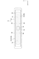
図1に示されるように、本実施形態に係るRFIDタグ10は、基材12、アンテナパターン14、ICチップ16、接着材18、第一粘着層20、第一ラミネートフィルム22、第二粘着層24、第二ラミネートフィルム26、及び、ゴム被覆材28を備える。
As shown in FIG. 1, the
基材12は、平面視で長方形のシート状(板状)に形成されている。各図において、矢印X、矢印Y、矢印Zは、基材12の長さ方向(長手方向)、幅方向(短手方向)、厚み方向をそれぞれ示している。基材12の幅方向は、基材12の平面視で基材12の長さ方向と直交する方向であり、基材12の厚み方向は、基材12の側面視で基材12の長さ方向と直交する方向である。基材12の長さ方向、幅方向、厚み方向は、RFIDタグ10の長さ方向、幅方向、厚み方向と同じである。
The
アンテナパターン14は、基材12の表面(アンテナパターン14が形成された一方の面)に形成されており、基材12の長さ方向に延びている。このアンテナパターン14は、例えば、銀ペーストやアルミ箔等の金属材料により形成される。本実施形態において、アンテナパターン14は、一例として、直線状に形成されている。
The
IC(Integrated Circuit)チップ16は、基材12の表面に搭載されており、接着材18を介して基材12の表面に接着されている。このICチップ16は、基材12の長さ方向及び幅方向の中央部に配置されており、アンテナパターン14と接続されている。
The IC (Integrated Circuit)
第一粘着層20は、「粘着層」の一例であり、第一ラミネートフィルム22は、「ラミネートフィルム」の一例である。第一粘着層20及び第一ラミネートフィルム22は、基材12の表側(アンテナパターン14及びICチップ16が配置された側)に配置されている。この第一粘着層20及び第一ラミネートフィルム22は、基材12と略同じ形状及び大きさを有している。第一粘着層20は、基材12の表面、アンテナパターン14、及び、ICチップ16を覆っており、第一ラミネートフィルム22は、第一粘着層20を介して基材12の表面に接着されている。
The first
第二粘着層24及び第二ラミネートフィルム26は、基材12の裏側(アンテナパターン14及びICチップ16が配置された側と反対側)に配置されている。この第二粘着層24及び第二ラミネートフィルム26も、第一粘着層20及び第一ラミネートフィルム22と同様に、基材12と略同じ形状及び大きさを有している。第二粘着層24は、第一粘着層20と反対側から基材12の裏面(アンテナパターン14が形成された一方の面と反対側の他方の面)を覆っており、第二ラミネートフィルム26は、第二粘着層24を介して基材12の裏面に接着されている。
The second
上述の基材12、第一粘着層20、第一ラミネートフィルム22、第二粘着層24、及び、第二ラミネートフィルム26は、RFIDタグ10の本体であるタグ本体30(インレット)を形成している。基材12、第一ラミネートフィルム22、及び、第二ラミネートフィルム26は、いずれもプラスチック製であり、可撓性を有している。
The
この基材12、第一ラミネートフィルム22、及び、第二ラミネートフィルム26には、例えば、ポリエチレンテレフタレート(PET: Polyethylene terephthalate)や、ポリエチレンナフタレート(PEN: Polyethylene Naphthalate)等の材料が適用される。一方、第一粘着層20及び第二粘着層24には、例えば、アクリル系やゴム系等の材料が適用される。
A material such as polyethylene terephthalate (PET) or polyethylene naphthalate (PEN) is applied to the
ところで、本実施形態に係るRFIDタグ10は、例えば水や薬品等の液体を使用する環境で使用されることが想定される。この場合に、例えば水や薬品等の液体がRFIDタグ10にかかると、第一粘着層20及び第二粘着層24の外周部から液体が第一粘着層20及び第二粘着層24の内側へ浸透し、第一粘着層20及び第二粘着層24が損傷する虞がある。また、液体が第一粘着層20の内側へ浸透すると、液体がアンテナパターン14やICチップ16に到達し、アンテナパターン14が腐食したり、ICチップ16が故障したりする虞がある。
By the way, it is assumed that the
そこで、本実施形態に係るRFIDタグ10では、液体が第一粘着層20及び第二粘着層24の内側へ浸透することを抑止するために、RFIDタグ10に第一封止部32及び第二封止部34が設けられている。
Therefore, in the
第一封止部32は、「封止部」の一例である。この第一封止部32は、第一ラミネートフィルム22の一部が基材12に溶着されることにより形成されている。具体的には、第一封止部32は、第一ラミネートフィルム22の一部が基材12側に凸を成すように変形されて形成されている。また、この基材12側に凸を成す第一封止部32の先端部は、基材12の表面に接合されている。この第一封止部32は、第一粘着層20の外周部に沿って形成されており、平面視でアンテナパターン14及びICチップ16を囲う環状を成している。
The
第二封止部34は、第一封止部32と同様に、第二ラミネートフィルム26の一部が基材12に溶着されることにより形成されている。この第二封止部34も、上述の第一封止部32と同様に、第二ラミネートフィルム26の一部が基材12側に凸を成すように変形されて形成されている。また、この基材12側に凸を成す第二封止部34の先端部は、基材12の裏面に接合されている。この第二封止部34も、平面視で環状を成している。なお、図1及び以下に説明する各図の平面図では、第一封止部32及び第二封止部34が破線により簡略化して図示されている。
The
本実施形態では、一例として、第一封止部32及び第二封止部34は、例えば超音波溶着又は熱溶着等の溶着加工により同時に形成されている。つまり、第一ラミネートフィルム22及び第二ラミネートフィルム26の同じ位置を厚さ方向の両側から溶着工具で挟み込むことにより、第一封止部32及び第二封止部34は、同時に形成されている。そして、これにより、第一封止部32及び第二封止部34は、平面視で互いに重複する位置、すなわち、平面視で同じ形状及び大きさで且つ基材12の長さ方向及び幅方向の同じ位置に形成されている。
In the present embodiment, as an example, the
ゴム被覆材28は、第一封止部32及び第二封止部34が形成された後にタグ本体30と一体化されたものであり、タグ本体30を包囲している。ゴム被覆材28を有するRFIDタグ10全体は、長尺板状を成している。なお、図1では、RFIDタグ10の内部構造の理解の容易のために、RFIDタグ10が厚み方向に誇張して示されている。
The
次に、本実施形態の作用及び効果について説明する。 Next, the operation and effect of this embodiment will be described.
以上詳述したように、本実施形態に係るRFIDタグ10によれば、第一ラミネートフィルム22には、この第一ラミネートフィルム22の一部が基材12に溶着されることにより、第一封止部32が形成されている。この第一封止部32は、平面視でアンテナパターン14及びICチップ16を囲う環状に形成されている。したがって、例えば水や薬品等の液体がRFIDタグ10にかかった場合でも、第一粘着層20の外周部から液体が第一粘着層20の内側へ浸透することを第一封止部32により抑止することができる。これにより、第一粘着層20が損傷することを抑制することができる。また、液体が第一粘着層20を通じてアンテナパターン14やICチップ16に到達することも抑止することができるので、アンテナパターン14が腐食したり、ICチップ16が故障したりすることを抑制することができる。
As described in detail above, according to the
また、第二ラミネートフィルム26には、第一ラミネートフィルム22と同様に、第二ラミネートフィルム26の一部が基材12に溶着されることにより、第二封止部34が形成されている。この第二封止部34も、第一封止部32と同様に、環状に形成されている。したがって、例えば水や薬品等の液体がRFIDタグ10にかかった場合でも、第二粘着層24の外周部から液体が第二粘着層24の内側へ浸透することを第二封止部34により抑止することができる。これにより、第二粘着層24が損傷することを抑制することができる。
Further, in the second
また、第一封止部32及び第二封止部34は、平面視で互いに重複する位置に形成されている。このように、第一封止部32及び第二封止部34を平面視で互いに重複する位置に形成するには、第一封止部32及び第二封止部34を例えば超音波溶着又は熱溶着等の溶着加工により同時に形成すれば良い。したがって、第一封止部32及び第二封止部34を溶着加工により同時に形成することにより、加工工数の増加、ひいては、製造コストを抑制することができる。
Further, the
また、第一封止部32及び第二封止部34は、第一粘着層20及び第二粘着層24の外周部に沿って形成されている。したがって、例えば水や薬品等の液体がRFIDタグ10にかかった場合でも、第一粘着層20及び第二粘着層24の外周部に近い側で液体の浸透を阻止することができる。これにより、液体の浸透により第一粘着層20及び第二粘着層24に影響が生じる範囲を狭める(第一粘着層20及び第二粘着層24の外周部側に留める)ことができる。
Further, the
また、本実施形態に係るRFIDタグ10は、ゴム被覆材28を有しており、このゴム被覆材28は、基材12、アンテナパターン14、ICチップ16等を有するタグ本体30を包囲している。したがって、第一粘着層20及び第二粘着層24の外周部から液体が第一粘着層20及び第二粘着層24の内側へ浸透することをゴム被覆材28によってより一層効果的に抑止することができる。
Further, the
また、タグ本体30は、ゴム被覆材28に包囲されている。したがって、例えばRFIDタグ10が二つ折りに折り曲げられた場合でも、この二つ折りに折り曲げられたRFIDタグ10の内側でゴム被覆材28のゴム層同士が干渉する。これにより、タグ本体30の曲率半径が一定以下になることを抑制することができるので、第一封止部32及び第二封止部34の破損を抑制することができる。
Further, the
なお、RFIDタグ10の使用時にRFIDタグ10に繰り返し応力が作用すると、ゴム被覆材28に破れや亀裂等の損傷部位が生じ、この損傷部位から液体が浸入する虞がある。しかしながら、上述のように、第一ラミネートフィルム22及び第二ラミネートフィルム26には、第一封止部32及び第二封止部34が形成されている。したがって、ゴム被覆材28に破れや亀裂等の損傷部位が生じても、第一粘着層20及び第二粘着層24の外周部から液体が第一粘着層20及び第二粘着層24の内側へ浸透することを抑止することができる。
If stress is repeatedly applied to the
次に、本実施形態の変形例について説明する。 Next, a modified example of this embodiment will be described.
上記実施形態において、第一封止部32及び第二封止部34は、平面視で互いに重複する位置、すなわち、平面視で同じ形状及び大きさで且つ同じ位置に形成されている。しかしながら、第一封止部32及び第二封止部34は、互いに異なる形状で且つ異なる位置に形成されていても良い。
In the above embodiment, the
例えば、図2に示される例において、第一封止部32は、平面視で第二封止部34の外側に形成されている。また、図3に示される例において、第一封止部32は、平面視で第二封止部34の内側に形成されている。
For example, in the example shown in FIG. 2, the
このように、平面視で第一封止部32及び第二封止部34の位置がずれていると、第一封止部32及び第二封止部34が平面視で互いに重複する位置に形成された場合に比して、第一封止部32及び第二封止部34によって曲げ剛性が高められた範囲が拡がる。これにより、RFIDタグ10の曲げ剛性を高めることができ、ひいては、アンテナパターン14やICチップ16の折れを抑制することができる。
In this way, if the positions of the
また、上記実施形態において、基材12の表側には、第一ラミネートフィルム22が一重に設けられている。しかしながら、図4に示されるように、基材12の表側には、第一ラミネートフィルム22が二重に設けられていても良い。なお、図4に示される例において、二重の第一ラミネートフィルム22及びこれに付随する二重の第一粘着層20及び二重の第一封止部32をそれぞれ区別する場合には、各符号の末尾に識別符号を「1」、「2」を付与することとする。
Further, in the above embodiment, the first
この図4に示される例において、外側の第一粘着層20−2及び外側の第一ラミネートフィルム22−2は、平面視で内側の第一粘着層20−1及び内側の第一ラミネートフィルム22−1よりも大きく形成されている。この外側の第一粘着層20−2及び外側の第一ラミネートフィルム22−2は、平面視で基材12と同様の形状及び大きさを有している。
In the example shown in FIG. 4, the outer first adhesive layer 20-2 and the outer first laminated film 22-2 are the inner first adhesive layer 20-1 and the inner first
また、外側の第一粘着層20−2は、内側の第一ラミネートフィルム22−1及び基材12を覆っている。この外側の第一ラミネートフィルム22−2は、外側の第一粘着層20−2を介して内側の第一ラミネートフィルム22−1及び基材12に接着されている。この外側の第一粘着層20−2及び外側の第一ラミネートフィルム22−2は、内側の第一粘着層20−1及び内側の第一ラミネートフィルム22−1とそれぞれ同様の材料で形成される。
Further, the outer first adhesive layer 20-2 covers the inner first laminated film 22-1 and the
また、外側の第一ラミネートフィルム22−2の外周部側は、内側の第一ラミネートフィルム22−1よりも外側にはみ出している。この第一ラミネートフィルム22の外周部側には、内側の第一封止部32−1と同様の形状の外側の第一封止部32−2が形成されている。
Further, the outer peripheral side of the outer first laminated film 22-2 protrudes outward from the inner first laminated film 22-1. On the outer peripheral side of the first
つまり、外側の第一封止部32−2は、外側の第一ラミネートフィルム22−2の一部が基材12に溶着されることにより形成されている。具体的には、外側の第一封止部32−2は、外側の第一ラミネートフィルム22−2の一部が基材12側に凸を成すように変形されて形成されている。また、この基材12側に凸を成す第一封止部32の先端部は、内側の第一ラミネートフィルム22−1の外側において、基材12の表面に接合されている。
That is, the outer first sealing portion 32-2 is formed by welding a part of the outer first laminated film 22-2 to the
また、外側の第一封止部32−2は、第一粘着層20の外周部に沿って形成されている。この外側の第一封止部32−2は、平面視で内側の第一粘着層20−1及び第一ラミネートフィルム22−1を囲う環状を成しており、且つ、平面視で内側の第一封止部32−1の外側に形成されている。
Further, the outer first sealing portion 32-2 is formed along the outer peripheral portion of the first
なお、内側の第一粘着層20−1は、「内側粘着層」の一例であり、内側の第一ラミネートフィルム22−1は、「内側ラミネートフィルム」の一例であり、内側の第一封止部32−1は、「内側封止部」の一例である。また、外側の第一粘着層20−2は、「外側粘着層」の一例であり、外側の第一ラミネートフィルム22−2は、「外側ラミネートフィルム」の一例であり、外側の第一封止部32−2は、「外側封止部」の一例である。 The inner first adhesive layer 20-1 is an example of the "inner adhesive layer", and the inner first laminated film 22-1 is an example of the "inner laminated film", and the inner first sealing is provided. Part 32-1 is an example of an "inner sealing part". Further, the outer first adhesive layer 20-2 is an example of the "outer adhesive layer", and the outer first laminated film 22-2 is an example of the "outer laminated film", and the outer first sealing is provided. Part 32-2 is an example of the "outer sealing part".
このように、基材12の表側に二重の第一ラミネートフィルム22が設けられ、且つ、二重の第一ラミネートフィルム22に第一封止部32がそれぞれ形成されていると、封止構造を二重にすることができる。これにより、液体が第一粘着層20を通じてアンテナパターン14やICチップ16に到達することをより一層効果的に抑止することができる。
As described above, when the double first
なお、本例において、基材12の表側には、二重の第一ラミネートフィルム22が設けられているが、基材12の表側には、三重以上の第一ラミネートフィルム22が設けられていても良い。
In this example, the double first
また、本例において、基材12の裏側は、一重の第二ラミネートフィルム26が設けられているが、基材12の裏側にも、二重以上の第二ラミネートフィルム26が設けられても良い。
Further, in this example, the back side of the
また、上記実施形態では、基材12の裏側に第二粘着層24及び第二ラミネートフィルム26が設けられている。しかしながら、図5に示されるように、基材12の裏側から上述の第二粘着層24及び第二ラミネートフィルム26(図1等参照)が省かれても良い。このように構成されていると、RFIDタグ10の構造を簡素化することができる。
Further, in the above embodiment, the second
また、上記実施形態において、第一封止部32及び第二封止部34は、平面視で四角形を成しており、第一封止部32及び第二封止部34の各辺部は、直線状に形成されている。しかしながら、図6に示されるように、第一封止部32及び第二封止部34の各長辺部には、屈曲部36がそれぞれ形成されていても良い。各屈曲部36は、基材12の幅方向中央側に凸を成すように平面視でV字状を成している。また、各屈曲部36は、ICチップ16及び接着材18に対して基材12の長さ方向にずれて位置している。
Further, in the above embodiment, the
ICチップ16及び接着材18に対して基材12の長さ方向一方側にずれて形成された一対の屈曲部36は、互いに基材12の幅方向に対向する位置(基材12の長さ方向の同じ位置)に形成されている。同様に、ICチップ16及び接着材18に対して基材12の長さ方向他方側にずれて形成された一対の屈曲部36は、互いに基材12の幅方向に対向する位置に形成されている。第一封止部32に係止された屈曲部36と、第二封止部34に形成された屈曲部36は、平面視で同じ形状及び位置に形成されている。
The pair of
このように、図6に示される例では、第一封止部32及び第二封止部34に屈曲部36が形成され、且つ、この屈曲部36がICチップ16及び接着材18に対して基材12の長さ方向にずれて位置している。したがって、RFIDタグ10に曲げ力が作用した場合でも、屈曲部36を起点にRFIDタグ10が折れ曲がり易くなる。これにより、ICチップ16及び接着材18とアンテナパターン14との境界部を起点にRFIDタグ10が折れ曲がることを抑制でき、ひいては、アンテナパターン14の断線を抑制することができる。
As described above, in the example shown in FIG. 6, the
なお、図6に示される例では、第一封止部32及び第二封止部34に平面視でV字状の屈曲部36が形成されているが、屈曲部36の代わりに、図7に示されるように、第一封止部32及び第二封止部34に平面視で円弧状の湾曲部38が形成されていても良い。このように構成されていても、RFIDタグ10に曲げ力が作用した場合には、湾曲部38を起点にRFIDタグ10を折れ曲がり易くすることができる。
In the example shown in FIG. 6, a V-shaped
また、図8に示されるように、第一封止部32及び第二封止部34は、平面視で波形に形成されていても良い。この図8に示される例において、第一封止部32及び第二封止部34は、平面視で同じ形状の波形に形成されているが、第一封止部32及び第二封止部34は、平面視で異なる形状の波形に形成されていても良い。
Further, as shown in FIG. 8, the
このように、図8に示される例では、第一封止部32及び第二封止部34が平面視で波形に形成されている。したがって、例えば、第一封止部32及び第二封止部34の各辺部が直線状に形成された場合に比して、第一封止部32及び第二封止部34によって補強された部位を拡げることができる。これにより、RFIDタグ10の曲げ剛性を向上させることができる。
As described above, in the example shown in FIG. 8, the
また、上記実施形態において、第一ラミネートフィルム22及び第二ラミネートフィルム26には、第一封止部32及び第二封止部34が一重に形成されている。しかしながら、図9に示されるように、第一ラミネートフィルム22及び第二ラミネートフィルム26には、第一封止部32及び第二封止部34がそれぞれ二重に形成されていても良い。また、第一ラミネートフィルム22及び第二ラミネートフィルム26には、第一封止部32及び第二封止部34がそれぞれ三重以上に形成されていても良い。このように構成されていると、多重環状を成す第一封止部32及び第二封止部34による封止性を向上させることができる。
Further, in the above embodiment, the
また、図10に示されるように、第一ラミネートフィルム22及び第二ラミネートフィルム26には、複数の第一封止部32を繋ぐ第一連結部40、及び、複数の第二封止部34を繋ぐ第二連結部42がそれぞれ形成されても良い。第一連結部40は、「連結部」の一例である。この第一連結部40及び第二連結部42も、第一封止部32及び第二封止部34と同様に、第一ラミネートフィルム22及び第二ラミネートフィルム26の一部が基材12に溶着されて形成されている。このように構成されていると、第一封止部32及び第二封止部34による封止性をより向上させることができると共に、RFIDタグ10の曲げ剛性を高めることができる。
Further, as shown in FIG. 10, the first
また、上記実施形態において、アンテナパターン14は、直線状に延びている。しかしながら、図11に示されるように、アンテナパターン14は、屈曲して形成されていても良い。また、この場合に、第一封止部32及び第二封止部34は、アンテナパターン14に沿って屈曲して形成されていても良い。
Further, in the above embodiment, the
また、アンテナパターン14は、湾曲して形成されていても良く、この場合に、第一封止部32及び第二封止部34は、アンテナパターン14に沿って湾曲して形成されていても良い。
Further, the
また、上記実施形態において、RFIDタグ10は、平面視で長方形状に形成されているが、例えば、平面視で正方形状、円形状、楕円形状など、長方形状以外の形状に形成されていても良い。
Further, in the above embodiment, the
なお、上記複数の変形例のうち、組み合わせ可能な変形例は、適宜、組み合わされて実施されても良い。 Of the above-mentioned plurality of modified examples, the modified examples that can be combined may be appropriately combined and carried out.
以上、本願の開示する技術の一実施形態について説明したが、本願の開示する技術は、上記に限定されるものでなく、上記以外にも、その主旨を逸脱しない範囲内において種々変形して実施可能であることは勿論である。 Although one embodiment of the technique disclosed in the present application has been described above, the technique disclosed in the present application is not limited to the above, and other than the above, various modifications are performed within a range not deviating from the gist thereof. Of course it is possible.
なお、上述の本願の開示する技術の一実施形態に関し、更に以下の付記を開示する。 The following additional notes will be further disclosed with respect to one embodiment of the above-mentioned technique disclosed in the present application.
(付記1)
シート状に形成されたプラスチック製の基材と、
前記基材に形成されたアンテナパターンと、
前記基材に搭載されると共に、前記アンテナパターンと接続されたICチップと、
前記基材、前記アンテナパターン、及び、前記ICチップを覆う粘着層と、
前記粘着層を介して前記基材に接着されたプラスチック製のラミネートフィルムと、
前記ラミネートフィルムの一部が前記基材に溶着されて形成され、平面視で前記アンテナパターン及びICチップを囲う環状の封止部と、
を備えるRFIDタグ。
(付記2)
前記基材、前記アンテナパターン、前記ICチップ、前記粘着層、前記ラミネートフィルム、前記封止部は、タグ本体を形成し、
前記タグ本体を包囲するゴム被覆材をさらに備える、
付記1に記載のRFIDタグ。
(付記3)
前記封止部は、前記粘着層の外周部に沿って形成されている、
付記1又は付記2に記載のRFIDタグ。
(付記4)
前記粘着層としての第一粘着層と、
前記ラミネートフィルムとしての第一ラミネートフィルムと、
前記封止部としての第一封止部と、
前記第一粘着層と反対側から前記基材を覆う第二粘着層と、
前記第二粘着層を介して前記基材に接着されたプラスチック製の第二ラミネートフィルムと、
前記第二ラミネートフィルムの一部が前記基材に溶着されて形成された環状の第二封止部と、
を備える、
付記1〜付記3のいずれか一項に記載のRFIDタグ。
(付記5)
前記第一封止部及び前記第二封止部は、平面視で互いに重複する位置に形成されている、
付記4に記載のRFIDタグ。
(付記6)
前記第一封止部は、平面視で前記第二封止部の外側に形成されている、
付記4に記載のRFIDタグ。
(付記7)
前記第一封止部は、平面視で前記第二封止部の内側に形成されている、
付記4に記載のRFIDタグ。
(付記8)
前記粘着層としての内側粘着層と、
前記ラミネートフィルムとしての内側ラミネートフィルムと、
前記封止部としての内側封止部と、
前記内側ラミネートフィルム及び前記基材を覆う外側粘着層と、
前記外側粘着層を介して前記内側ラミネートフィルム及び前記基材に接着されたプラスチック製の外側ラミネートフィルムと、
前記外側ラミネートフィルムの一部が前記内側ラミネートフィルムに溶着されて形成され、平面視で前記内側粘着層及び前記内側ラミネートフィルムを囲う環状の外側封止部と、
を備える、
付記1〜付記7のいずれか一項に記載のRFIDタグ。
(付記9)
前記ICチップは、接着材を介して前記基材に接着され、
前記封止部には、前記接着材に対して前記基材の長さ方向にずれて位置し、平面視でV字状を成す屈曲部が形成されている、
付記1〜付記8のいずれか一項に記載のRFIDタグ。
(付記10)
前記ICチップは、接着材を介して前記基材に接着され、
前記封止部には、前記ICチップ及び前記接着材に対して前記基材の長さ方向にずれて位置し、平面視で円弧状を成す湾曲部が形成されている、
付記1〜付記8のいずれか一項に記載のRFIDタグ。
(付記11)
前記封止部は、平面視で波形に形成されている、
付記1〜付記10のいずれか一項に記載のRFIDタグ。
(付記12)
多重環状を成す複数の前記封止部を備える、
付記1〜付記11のいずれか一項に記載のRFIDタグ。
(付記13)
前記ラミネートフィルムの一部が前記基材に溶着されて形成され、複数の前記封止部を繋ぐ連結部を備える、
付記12に記載のRFIDタグ。
(Appendix 1)
A sheet-shaped plastic base material and
The antenna pattern formed on the base material and
An IC chip mounted on the base material and connected to the antenna pattern,
The base material, the antenna pattern, and the adhesive layer covering the IC chip,
A plastic laminate film adhered to the substrate via the adhesive layer, and
A part of the laminated film is welded to the base material to form an annular sealing portion that surrounds the antenna pattern and the IC chip in a plan view.
RFID tag with.
(Appendix 2)
The base material, the antenna pattern, the IC chip, the adhesive layer, the laminated film, and the sealing portion form a tag body.
A rubber coating material surrounding the tag body is further provided.
The RFID tag described in Appendix 1.
(Appendix 3)
The sealing portion is formed along the outer peripheral portion of the adhesive layer.
The RFID tag according to Appendix 1 or Appendix 2.
(Appendix 4)
The first adhesive layer as the adhesive layer and
The first laminated film as the laminated film and
The first sealing portion as the sealing portion and
A second adhesive layer covering the base material from the side opposite to the first adhesive layer,
A second laminated film made of plastic adhered to the base material via the second adhesive layer, and
An annular second sealing portion formed by welding a part of the second laminated film to the base material,
To prepare
The RFID tag according to any one of Supplementary note 1 to Supplementary note 3.
(Appendix 5)
The first sealing portion and the second sealing portion are formed at positions overlapping each other in a plan view.
The RFID tag described in Appendix 4.
(Appendix 6)
The first sealing portion is formed on the outside of the second sealing portion in a plan view.
The RFID tag described in Appendix 4.
(Appendix 7)
The first sealing portion is formed inside the second sealing portion in a plan view.
The RFID tag described in Appendix 4.
(Appendix 8)
The inner adhesive layer as the adhesive layer and
The inner laminate film as the laminate film and
The inner sealing portion as the sealing portion and the inner sealing portion
The inner laminated film and the outer adhesive layer covering the base material,
With the inner laminate film and the plastic outer laminate film adhered to the substrate via the outer adhesive layer,
A part of the outer laminated film is formed by welding to the inner laminated film, and in a plan view, the inner adhesive layer and the annular outer sealing portion surrounding the inner laminated film are formed.
To prepare
The RFID tag according to any one of Supplementary note 1 to Supplementary note 7.
(Appendix 9)
The IC chip is adhered to the base material via an adhesive, and the IC chip is adhered to the base material.
The sealing portion is formed with a bent portion that is positioned with respect to the adhesive material in the length direction of the base material and has a V shape in a plan view.
The RFID tag according to any one of Supplementary note 1 to Supplementary note 8.
(Appendix 10)
The IC chip is adhered to the base material via an adhesive, and the IC chip is adhered to the base material.
The sealing portion is formed with a curved portion that is positioned with respect to the IC chip and the adhesive material in the length direction of the base material and forms an arc shape in a plan view.
The RFID tag according to any one of Supplementary note 1 to Supplementary note 8.
(Appendix 11)
The sealing portion is formed in a wavy shape in a plan view.
The RFID tag according to any one of Supplementary note 1 to
(Appendix 12)
It is provided with a plurality of the sealing portions forming a multiple ring.
The RFID tag according to any one of Supplementary note 1 to Supplementary note 11.
(Appendix 13)
A part of the laminated film is formed by welding to the base material, and includes a connecting portion for connecting the plurality of sealing portions.
The RFID tag according to
10 RFIDタグ
12 基材
14 アンテナパターン
16 ICチップ
18 接着材
20 第一粘着層(粘着層の一例)
22 第一ラミネートフィルム(ラミネートフィルムの一例)
24 第二粘着層
26 第二ラミネートフィルム
28 ゴム被覆材
30 タグ本体
32 第一封止部(封止部の一例)
34 第二封止部
36 屈曲部
38 湾曲部
40 第一連結部(連結部の一例)
42 第二連結部
10
22 First laminated film (an example of laminated film)
24
34
42 Second connecting part
Claims (7)
前記基材に形成されたアンテナパターンと、
前記基材に搭載されると共に、前記アンテナパターンと接続されたICチップと、
前記基材、前記アンテナパターン、及び、前記ICチップを覆う粘着層と、
前記粘着層を介して前記基材に接着されたプラスチック製のラミネートフィルムと、
前記ラミネートフィルムの一部が前記基材側に凸を成し前記基材に溶着されて形成され、平面視で前記アンテナパターン及びICチップを囲う環状の封止部と、
を備えるRFIDタグ。 A sheet-shaped plastic base material and
The antenna pattern formed on the base material and
An IC chip mounted on the base material and connected to the antenna pattern,
The base material, the antenna pattern, and the adhesive layer covering the IC chip,
A plastic laminate film adhered to the substrate via the adhesive layer, and
A part of the laminated film is formed by being welded to the base material so as to be convex on the base material side, and an annular sealing portion surrounding the antenna pattern and the IC chip in a plan view and an annular sealing portion.
RFID tag with.
前記タグ本体を包囲するゴム被覆材をさらに備える、
請求項1に記載のRFIDタグ。 The base material, the antenna pattern, the IC chip, the adhesive layer, the laminate film, and the sealing portion form a tag body.
A rubber coating material surrounding the tag body is further provided.
The RFID tag according to claim 1.
請求項1又は請求項2に記載のRFIDタグ。 The sealing portion is formed along the outer peripheral portion of the adhesive layer.
The RFID tag according to claim 1 or 2.
前記ラミネートフィルムとしての第一ラミネートフィルムと、
前記封止部としての第一封止部と、
前記第一粘着層と反対側から前記基材を覆う第二粘着層と、
前記第二粘着層を介して前記基材に接着されたプラスチック製の第二ラミネートフィルムと、
前記第二ラミネートフィルムの一部が前記基材に溶着されて形成された環状の第二封止部と、
を備える、
請求項1〜請求項3のいずれか一項に記載のRFIDタグ。 The first adhesive layer as the adhesive layer and
The first laminated film as the laminated film and
The first sealing portion as the sealing portion and
A second adhesive layer covering the base material from the side opposite to the first adhesive layer,
A second laminated film made of plastic adhered to the base material via the second adhesive layer, and
An annular second sealing portion formed by welding a part of the second laminated film to the base material,
To prepare
The RFID tag according to any one of claims 1 to 3.
請求項4に記載のRFIDタグ。 The first sealing portion and the second sealing portion are formed at positions overlapping each other in a plan view.
The RFID tag according to claim 4.
前記基材に形成されたアンテナパターンと、
前記基材に搭載されると共に、前記アンテナパターンと接続されたICチップと、
前記基材、前記アンテナパターン、及び、前記ICチップを覆う第一粘着層と、
前記第一粘着層を介して前記基材に接着されたプラスチック製の第一ラミネートフィルムと、
前記第一ラミネートフィルムの一部が前記基材に溶着されて形成され、平面視で前記アンテナパターン及びICチップを囲う環状の第一封止部と、
前記第一粘着層と反対側から前記基材を覆う第二粘着層と、
前記第二粘着層を介して前記基材に接着されたプラスチック製の第二ラミネートフィルムと、
前記第二ラミネートフィルムの一部が前記基材に溶着されて形成された環状の第二封止部と、
を備え、
前記第一封止部は、平面視で前記第二封止部の外側又は内側に形成されている、
RFIDタグ。 A sheet-shaped plastic base material and
The antenna pattern formed on the base material and
An IC chip mounted on the base material and connected to the antenna pattern,
The base material, the antenna pattern, and the first adhesive layer covering the IC chip,
A first laminated film made of plastic adhered to the base material via the first adhesive layer,
A part of the first laminated film is welded to the base material to form an annular first sealing portion that surrounds the antenna pattern and the IC chip in a plan view.
A second adhesive layer covering the base material from the side opposite to the first adhesive layer,
A second laminated film made of plastic adhered to the base material via the second adhesive layer, and
An annular second sealing portion formed by welding a part of the second laminated film to the base material,
With
The first sealing portion is formed on the outside or inside of the second sealing portion in a plan view.
R FID tag.
前記ラミネートフィルムとしての内側ラミネートフィルムと、
前記封止部としての内側封止部と、
前記内側ラミネートフィルム及び前記基材を覆う外側粘着層と、
前記外側粘着層を介して前記内側ラミネートフィルム及び前記基材に接着されたプラスチック製の外側ラミネートフィルムと、
前記外側ラミネートフィルムの一部が内側ラミネートフィルムよりも外側で前記基材に溶着されて形成され、平面視で前記内側粘着層及び前記内側ラミネートフィルムを囲う環状の外側封止部と、
を備える、
請求項1〜請求項5のいずれか一項に記載のRFIDタグ。 The inner adhesive layer as the adhesive layer and
The inner laminate film as the laminate film and
The inner sealing portion as the sealing portion and the inner sealing portion
The inner laminated film and the outer adhesive layer covering the base material,
With the inner laminate film and the plastic outer laminate film adhered to the substrate via the outer adhesive layer,
A part of the outer laminated film is formed by welding to the base material on the outer side of the inner laminated film , and in a plan view, the inner adhesive layer and the annular outer sealing portion surrounding the inner laminated film are formed.
To prepare
The RFID tag according to any one of claims 1 to 5.
Priority Applications (1)
| Application Number | Priority Date | Filing Date | Title |
|---|---|---|---|
| JP2017107609A JP6942315B2 (en) | 2017-05-31 | 2017-05-31 | RFID tag |
Applications Claiming Priority (1)
| Application Number | Priority Date | Filing Date | Title |
|---|---|---|---|
| JP2017107609A JP6942315B2 (en) | 2017-05-31 | 2017-05-31 | RFID tag |
Publications (2)
| Publication Number | Publication Date |
|---|---|
| JP2018205867A JP2018205867A (en) | 2018-12-27 |
| JP6942315B2 true JP6942315B2 (en) | 2021-09-29 |
Family
ID=64957759
Family Applications (1)
| Application Number | Title | Priority Date | Filing Date |
|---|---|---|---|
| JP2017107609A Active JP6942315B2 (en) | 2017-05-31 | 2017-05-31 | RFID tag |
Country Status (1)
| Country | Link |
|---|---|
| JP (1) | JP6942315B2 (en) |
Family Cites Families (3)
| Publication number | Priority date | Publication date | Assignee | Title |
|---|---|---|---|---|
| JP2009059153A (en) * | 2007-08-31 | 2009-03-19 | Dainippon Printing Co Ltd | Books and book manufacturing methods |
| JP5897386B2 (en) * | 2012-04-18 | 2016-03-30 | 富士通株式会社 | RFID tag |
| EP3944150A1 (en) * | 2015-04-07 | 2022-01-26 | Neology, Inc. | Radio frequency identification tag in a plate |
-
2017
- 2017-05-31 JP JP2017107609A patent/JP6942315B2/en active Active
Also Published As
| Publication number | Publication date |
|---|---|
| JP2018205867A (en) | 2018-12-27 |
Similar Documents
| Publication | Publication Date | Title |
|---|---|---|
| JP4815891B2 (en) | Wireless IC tag and antenna manufacturing method | |
| KR101237107B1 (en) | Antenna sheet, transponder and book form | |
| US8430324B2 (en) | RFID tag manufacturing method and RFID tag | |
| JP6028435B2 (en) | RFID tag | |
| TWI479425B (en) | Inquiry machine and booklet | |
| JP4676196B2 (en) | RFID tag | |
| JP4382802B2 (en) | RFID tag | |
| JP2009116649A (en) | RFID tag | |
| JP4768379B2 (en) | RFID tag | |
| JP6942315B2 (en) | RFID tag | |
| JP2003132331A (en) | Non-contact data carrier substrate and non-contact data carrier | |
| JP5082707B2 (en) | Label with IC tag and method of using label with IC tag | |
| JP2010257416A (en) | Information recording medium, data carrier with non-contact type IC, and method for manufacturing information recording medium | |
| JP2007122482A (en) | RFID tag and RFID tag manufacturing method | |
| US20160048750A1 (en) | Rfid tag | |
| JP5333137B2 (en) | IC tag manufacturing method | |
| JP6524009B2 (en) | IC card inlet, IC card, and method of manufacturing IC card | |
| CN118414619A (en) | Identification Label | |
| JP6786916B2 (en) | Non-contact crimping card and crimping card paper | |
| JP2013089163A (en) | Noncontact ic card | |
| HK1097071B (en) | A wireless ic tag and a method for manufacturing antenna | |
| JP2010160706A (en) | Contactless ic tags |
Legal Events
| Date | Code | Title | Description |
|---|---|---|---|
| A621 | Written request for application examination |
Free format text: JAPANESE INTERMEDIATE CODE: A621 Effective date: 20200203 |
|
| A977 | Report on retrieval |
Free format text: JAPANESE INTERMEDIATE CODE: A971007 Effective date: 20201111 |
|
| A131 | Notification of reasons for refusal |
Free format text: JAPANESE INTERMEDIATE CODE: A131 Effective date: 20201124 |
|
| A521 | Request for written amendment filed |
Free format text: JAPANESE INTERMEDIATE CODE: A523 Effective date: 20210125 |
|
| TRDD | Decision of grant or rejection written | ||
| A01 | Written decision to grant a patent or to grant a registration (utility model) |
Free format text: JAPANESE INTERMEDIATE CODE: A01 Effective date: 20210727 |
|
| A711 | Notification of change in applicant |
Free format text: JAPANESE INTERMEDIATE CODE: A711 Effective date: 20210804 |
|
| A61 | First payment of annual fees (during grant procedure) |
Free format text: JAPANESE INTERMEDIATE CODE: A61 Effective date: 20210820 |
|
| A521 | Request for written amendment filed |
Free format text: JAPANESE INTERMEDIATE CODE: A821 Effective date: 20210804 |
|
| R150 | Certificate of patent or registration of utility model |
Ref document number: 6942315 Country of ref document: JP Free format text: JAPANESE INTERMEDIATE CODE: R150 |
|
| R250 | Receipt of annual fees |
Free format text: JAPANESE INTERMEDIATE CODE: R250 |
|
| R250 | Receipt of annual fees |
Free format text: JAPANESE INTERMEDIATE CODE: R250 |