JP6923554B2 - Wiring boards, electronics and electronic modules - Google Patents
Wiring boards, electronics and electronic modules Download PDFInfo
- Publication number
- JP6923554B2 JP6923554B2 JP2018553017A JP2018553017A JP6923554B2 JP 6923554 B2 JP6923554 B2 JP 6923554B2 JP 2018553017 A JP2018553017 A JP 2018553017A JP 2018553017 A JP2018553017 A JP 2018553017A JP 6923554 B2 JP6923554 B2 JP 6923554B2
- Authority
- JP
- Japan
- Prior art keywords
- electrode
- wiring board
- insulating substrate
- thickness
- connecting portion
- Prior art date
- Legal status (The legal status is an assumption and is not a legal conclusion. Google has not performed a legal analysis and makes no representation as to the accuracy of the status listed.)
- Active
Links
- 239000000758 substrate Substances 0.000 claims description 126
- 229910000679 solder Inorganic materials 0.000 claims description 29
- 239000004020 conductor Substances 0.000 description 87
- 239000000919 ceramic Substances 0.000 description 55
- 238000004519 manufacturing process Methods 0.000 description 14
- 238000007747 plating Methods 0.000 description 13
- PXHVJJICTQNCMI-UHFFFAOYSA-N Nickel Chemical compound [Ni] PXHVJJICTQNCMI-UHFFFAOYSA-N 0.000 description 8
- 229910052751 metal Inorganic materials 0.000 description 8
- 239000002184 metal Substances 0.000 description 8
- 239000011347 resin Substances 0.000 description 8
- 229920005989 resin Polymers 0.000 description 8
- 238000000034 method Methods 0.000 description 7
- 239000004065 semiconductor Substances 0.000 description 7
- PCHJSUWPFVWCPO-UHFFFAOYSA-N gold Chemical compound [Au] PCHJSUWPFVWCPO-UHFFFAOYSA-N 0.000 description 6
- 229910052737 gold Inorganic materials 0.000 description 6
- 239000010931 gold Substances 0.000 description 6
- 239000000843 powder Substances 0.000 description 6
- 238000010304 firing Methods 0.000 description 5
- 238000010030 laminating Methods 0.000 description 5
- 238000007639 printing Methods 0.000 description 5
- 238000007650 screen-printing Methods 0.000 description 5
- 230000017525 heat dissipation Effects 0.000 description 4
- 229910052759 nickel Inorganic materials 0.000 description 4
- TWNQGVIAIRXVLR-UHFFFAOYSA-N oxo(oxoalumanyloxy)alumane Chemical compound O=[Al]O[Al]=O TWNQGVIAIRXVLR-UHFFFAOYSA-N 0.000 description 4
- 238000004080 punching Methods 0.000 description 4
- 239000011230 binding agent Substances 0.000 description 3
- 239000010949 copper Substances 0.000 description 3
- 239000011521 glass Substances 0.000 description 3
- 239000011572 manganese Substances 0.000 description 3
- 239000000463 material Substances 0.000 description 3
- 239000002904 solvent Substances 0.000 description 3
- RYGMFSIKBFXOCR-UHFFFAOYSA-N Copper Chemical compound [Cu] RYGMFSIKBFXOCR-UHFFFAOYSA-N 0.000 description 2
- KDLHZDBZIXYQEI-UHFFFAOYSA-N Palladium Chemical compound [Pd] KDLHZDBZIXYQEI-UHFFFAOYSA-N 0.000 description 2
- BQCADISMDOOEFD-UHFFFAOYSA-N Silver Chemical compound [Ag] BQCADISMDOOEFD-UHFFFAOYSA-N 0.000 description 2
- 239000011248 coating agent Substances 0.000 description 2
- 238000000576 coating method Methods 0.000 description 2
- 229910052802 copper Inorganic materials 0.000 description 2
- 238000005260 corrosion Methods 0.000 description 2
- 230000007797 corrosion Effects 0.000 description 2
- 238000005304 joining Methods 0.000 description 2
- 230000007774 longterm Effects 0.000 description 2
- 239000000395 magnesium oxide Substances 0.000 description 2
- CPLXHLVBOLITMK-UHFFFAOYSA-N magnesium oxide Inorganic materials [Mg]=O CPLXHLVBOLITMK-UHFFFAOYSA-N 0.000 description 2
- AXZKOIWUVFPNLO-UHFFFAOYSA-N magnesium;oxygen(2-) Chemical compound [O-2].[Mg+2] AXZKOIWUVFPNLO-UHFFFAOYSA-N 0.000 description 2
- 229910052748 manganese Inorganic materials 0.000 description 2
- 229910052750 molybdenum Inorganic materials 0.000 description 2
- 229910052709 silver Inorganic materials 0.000 description 2
- 239000004332 silver Substances 0.000 description 2
- 229910052721 tungsten Inorganic materials 0.000 description 2
- 229910018072 Al 2 O 3 Inorganic materials 0.000 description 1
- ODINCKMPIJJUCX-UHFFFAOYSA-N Calcium oxide Chemical compound [Ca]=O ODINCKMPIJJUCX-UHFFFAOYSA-N 0.000 description 1
- PWHULOQIROXLJO-UHFFFAOYSA-N Manganese Chemical compound [Mn] PWHULOQIROXLJO-UHFFFAOYSA-N 0.000 description 1
- ZOKXTWBITQBERF-UHFFFAOYSA-N Molybdenum Chemical compound [Mo] ZOKXTWBITQBERF-UHFFFAOYSA-N 0.000 description 1
- 229910004298 SiO 2 Inorganic materials 0.000 description 1
- VYPSYNLAJGMNEJ-UHFFFAOYSA-N Silicium dioxide Chemical compound O=[Si]=O VYPSYNLAJGMNEJ-UHFFFAOYSA-N 0.000 description 1
- PNEYBMLMFCGWSK-UHFFFAOYSA-N aluminium oxide Inorganic materials [O-2].[O-2].[O-2].[Al+3].[Al+3] PNEYBMLMFCGWSK-UHFFFAOYSA-N 0.000 description 1
- 238000005219 brazing Methods 0.000 description 1
- PMHQVHHXPFUNSP-UHFFFAOYSA-M copper(1+);methylsulfanylmethane;bromide Chemical compound Br[Cu].CSC PMHQVHHXPFUNSP-UHFFFAOYSA-M 0.000 description 1
- 239000013078 crystal Substances 0.000 description 1
- 238000007606 doctor blade method Methods 0.000 description 1
- 238000009713 electroplating Methods 0.000 description 1
- 239000002241 glass-ceramic Substances 0.000 description 1
- 238000009413 insulation Methods 0.000 description 1
- 238000004898 kneading Methods 0.000 description 1
- 238000002844 melting Methods 0.000 description 1
- 230000008018 melting Effects 0.000 description 1
- 238000012986 modification Methods 0.000 description 1
- 230000004048 modification Effects 0.000 description 1
- 239000011733 molybdenum Substances 0.000 description 1
- 238000000465 moulding Methods 0.000 description 1
- 229910052763 palladium Inorganic materials 0.000 description 1
- 238000003672 processing method Methods 0.000 description 1
- 230000005855 radiation Effects 0.000 description 1
- 239000002994 raw material Substances 0.000 description 1
- 239000003870 refractory metal Substances 0.000 description 1
- 238000005096 rolling process Methods 0.000 description 1
- 239000003566 sealing material Substances 0.000 description 1
- 229910052814 silicon oxide Inorganic materials 0.000 description 1
- 239000002002 slurry Substances 0.000 description 1
- 238000005476 soldering Methods 0.000 description 1
- 239000006188 syrup Substances 0.000 description 1
- 235000020357 syrup Nutrition 0.000 description 1
- WFKWXMTUELFFGS-UHFFFAOYSA-N tungsten Chemical compound [W] WFKWXMTUELFFGS-UHFFFAOYSA-N 0.000 description 1
- 239000010937 tungsten Substances 0.000 description 1
Images


Classifications
-
- H—ELECTRICITY
- H05—ELECTRIC TECHNIQUES NOT OTHERWISE PROVIDED FOR
- H05K—PRINTED CIRCUITS; CASINGS OR CONSTRUCTIONAL DETAILS OF ELECTRIC APPARATUS; MANUFACTURE OF ASSEMBLAGES OF ELECTRICAL COMPONENTS
- H05K3/00—Apparatus or processes for manufacturing printed circuits
- H05K3/40—Forming printed elements for providing electric connections to or between printed circuits
- H05K3/403—Edge contacts; Windows or holes in the substrate having plural connections on the walls thereof
-
- H—ELECTRICITY
- H01—ELECTRIC ELEMENTS
- H01L—SEMICONDUCTOR DEVICES NOT COVERED BY CLASS H10
- H01L23/00—Details of semiconductor or other solid state devices
- H01L23/48—Arrangements for conducting electric current to or from the solid state body in operation, e.g. leads, terminal arrangements ; Selection of materials therefor
- H01L23/488—Arrangements for conducting electric current to or from the solid state body in operation, e.g. leads, terminal arrangements ; Selection of materials therefor consisting of soldered or bonded constructions
- H01L23/498—Leads, i.e. metallisations or lead-frames on insulating substrates, e.g. chip carriers
- H01L23/49838—Geometry or layout
-
- H—ELECTRICITY
- H01—ELECTRIC ELEMENTS
- H01L—SEMICONDUCTOR DEVICES NOT COVERED BY CLASS H10
- H01L23/00—Details of semiconductor or other solid state devices
- H01L23/12—Mountings, e.g. non-detachable insulating substrates
-
- H—ELECTRICITY
- H01—ELECTRIC ELEMENTS
- H01L—SEMICONDUCTOR DEVICES NOT COVERED BY CLASS H10
- H01L23/00—Details of semiconductor or other solid state devices
- H01L23/12—Mountings, e.g. non-detachable insulating substrates
- H01L23/13—Mountings, e.g. non-detachable insulating substrates characterised by the shape
-
- H—ELECTRICITY
- H01—ELECTRIC ELEMENTS
- H01L—SEMICONDUCTOR DEVICES NOT COVERED BY CLASS H10
- H01L23/00—Details of semiconductor or other solid state devices
- H01L23/34—Arrangements for cooling, heating, ventilating or temperature compensation ; Temperature sensing arrangements
- H01L23/36—Selection of materials, or shaping, to facilitate cooling or heating, e.g. heatsinks
-
- H—ELECTRICITY
- H05—ELECTRIC TECHNIQUES NOT OTHERWISE PROVIDED FOR
- H05K—PRINTED CIRCUITS; CASINGS OR CONSTRUCTIONAL DETAILS OF ELECTRIC APPARATUS; MANUFACTURE OF ASSEMBLAGES OF ELECTRICAL COMPONENTS
- H05K1/00—Printed circuits
- H05K1/02—Details
- H05K1/11—Printed elements for providing electric connections to or between printed circuits
- H05K1/117—Pads along the edge of rigid circuit boards, e.g. for pluggable connectors
-
- H—ELECTRICITY
- H10—SEMICONDUCTOR DEVICES; ELECTRIC SOLID-STATE DEVICES NOT OTHERWISE PROVIDED FOR
- H10H—INORGANIC LIGHT-EMITTING SEMICONDUCTOR DEVICES HAVING POTENTIAL BARRIERS
- H10H20/00—Individual inorganic light-emitting semiconductor devices having potential barriers, e.g. light-emitting diodes [LED]
- H10H20/80—Constructional details
- H10H20/85—Packages
- H10H20/857—Interconnections, e.g. lead-frames, bond wires or solder balls
-
- H—ELECTRICITY
- H10—SEMICONDUCTOR DEVICES; ELECTRIC SOLID-STATE DEVICES NOT OTHERWISE PROVIDED FOR
- H10N—ELECTRIC SOLID-STATE DEVICES NOT OTHERWISE PROVIDED FOR
- H10N30/00—Piezoelectric or electrostrictive devices
- H10N30/80—Constructional details
- H10N30/87—Electrodes or interconnections, e.g. leads or terminals
- H10N30/875—Further connection or lead arrangements, e.g. flexible wiring boards, terminal pins
-
- H—ELECTRICITY
- H01—ELECTRIC ELEMENTS
- H01L—SEMICONDUCTOR DEVICES NOT COVERED BY CLASS H10
- H01L2224/00—Indexing scheme for arrangements for connecting or disconnecting semiconductor or solid-state bodies and methods related thereto as covered by H01L24/00
- H01L2224/01—Means for bonding being attached to, or being formed on, the surface to be connected, e.g. chip-to-package, die-attach, "first-level" interconnects; Manufacturing methods related thereto
- H01L2224/10—Bump connectors; Manufacturing methods related thereto
- H01L2224/15—Structure, shape, material or disposition of the bump connectors after the connecting process
- H01L2224/16—Structure, shape, material or disposition of the bump connectors after the connecting process of an individual bump connector
- H01L2224/161—Disposition
- H01L2224/16151—Disposition the bump connector connecting between a semiconductor or solid-state body and an item not being a semiconductor or solid-state body, e.g. chip-to-substrate, chip-to-passive
- H01L2224/16221—Disposition the bump connector connecting between a semiconductor or solid-state body and an item not being a semiconductor or solid-state body, e.g. chip-to-substrate, chip-to-passive the body and the item being stacked
- H01L2224/16225—Disposition the bump connector connecting between a semiconductor or solid-state body and an item not being a semiconductor or solid-state body, e.g. chip-to-substrate, chip-to-passive the body and the item being stacked the item being non-metallic, e.g. insulating substrate with or without metallisation
-
- H—ELECTRICITY
- H01—ELECTRIC ELEMENTS
- H01L—SEMICONDUCTOR DEVICES NOT COVERED BY CLASS H10
- H01L2224/00—Indexing scheme for arrangements for connecting or disconnecting semiconductor or solid-state bodies and methods related thereto as covered by H01L24/00
- H01L2224/01—Means for bonding being attached to, or being formed on, the surface to be connected, e.g. chip-to-package, die-attach, "first-level" interconnects; Manufacturing methods related thereto
- H01L2224/42—Wire connectors; Manufacturing methods related thereto
- H01L2224/47—Structure, shape, material or disposition of the wire connectors after the connecting process
- H01L2224/48—Structure, shape, material or disposition of the wire connectors after the connecting process of an individual wire connector
- H01L2224/4805—Shape
- H01L2224/4809—Loop shape
- H01L2224/48091—Arched
-
- H—ELECTRICITY
- H01—ELECTRIC ELEMENTS
- H01L—SEMICONDUCTOR DEVICES NOT COVERED BY CLASS H10
- H01L2224/00—Indexing scheme for arrangements for connecting or disconnecting semiconductor or solid-state bodies and methods related thereto as covered by H01L24/00
- H01L2224/01—Means for bonding being attached to, or being formed on, the surface to be connected, e.g. chip-to-package, die-attach, "first-level" interconnects; Manufacturing methods related thereto
- H01L2224/42—Wire connectors; Manufacturing methods related thereto
- H01L2224/47—Structure, shape, material or disposition of the wire connectors after the connecting process
- H01L2224/48—Structure, shape, material or disposition of the wire connectors after the connecting process of an individual wire connector
- H01L2224/481—Disposition
- H01L2224/48151—Connecting between a semiconductor or solid-state body and an item not being a semiconductor or solid-state body, e.g. chip-to-substrate, chip-to-passive
- H01L2224/48221—Connecting between a semiconductor or solid-state body and an item not being a semiconductor or solid-state body, e.g. chip-to-substrate, chip-to-passive the body and the item being stacked
- H01L2224/48225—Connecting between a semiconductor or solid-state body and an item not being a semiconductor or solid-state body, e.g. chip-to-substrate, chip-to-passive the body and the item being stacked the item being non-metallic, e.g. insulating substrate with or without metallisation
- H01L2224/48227—Connecting between a semiconductor or solid-state body and an item not being a semiconductor or solid-state body, e.g. chip-to-substrate, chip-to-passive the body and the item being stacked the item being non-metallic, e.g. insulating substrate with or without metallisation connecting the wire to a bond pad of the item
-
- H—ELECTRICITY
- H01—ELECTRIC ELEMENTS
- H01L—SEMICONDUCTOR DEVICES NOT COVERED BY CLASS H10
- H01L2924/00—Indexing scheme for arrangements or methods for connecting or disconnecting semiconductor or solid-state bodies as covered by H01L24/00
- H01L2924/15—Details of package parts other than the semiconductor or other solid state devices to be connected
- H01L2924/151—Die mounting substrate
- H01L2924/1517—Multilayer substrate
- H01L2924/15172—Fan-out arrangement of the internal vias
- H01L2924/15174—Fan-out arrangement of the internal vias in different layers of the multilayer substrate
-
- H—ELECTRICITY
- H01—ELECTRIC ELEMENTS
- H01L—SEMICONDUCTOR DEVICES NOT COVERED BY CLASS H10
- H01L2924/00—Indexing scheme for arrangements or methods for connecting or disconnecting semiconductor or solid-state bodies as covered by H01L24/00
- H01L2924/15—Details of package parts other than the semiconductor or other solid state devices to be connected
- H01L2924/181—Encapsulation
-
- H—ELECTRICITY
- H05—ELECTRIC TECHNIQUES NOT OTHERWISE PROVIDED FOR
- H05K—PRINTED CIRCUITS; CASINGS OR CONSTRUCTIONAL DETAILS OF ELECTRIC APPARATUS; MANUFACTURE OF ASSEMBLAGES OF ELECTRICAL COMPONENTS
- H05K1/00—Printed circuits
- H05K1/02—Details
- H05K1/11—Printed elements for providing electric connections to or between printed circuits
- H05K1/119—Details of rigid insulating substrates therefor, e.g. three-dimensional details
-
- H—ELECTRICITY
- H05—ELECTRIC TECHNIQUES NOT OTHERWISE PROVIDED FOR
- H05K—PRINTED CIRCUITS; CASINGS OR CONSTRUCTIONAL DETAILS OF ELECTRIC APPARATUS; MANUFACTURE OF ASSEMBLAGES OF ELECTRICAL COMPONENTS
- H05K2201/00—Indexing scheme relating to printed circuits covered by H05K1/00
- H05K2201/09—Shape and layout
- H05K2201/09145—Edge details
- H05K2201/09163—Slotted edge
-
- H—ELECTRICITY
- H05—ELECTRIC TECHNIQUES NOT OTHERWISE PROVIDED FOR
- H05K—PRINTED CIRCUITS; CASINGS OR CONSTRUCTIONAL DETAILS OF ELECTRIC APPARATUS; MANUFACTURE OF ASSEMBLAGES OF ELECTRICAL COMPONENTS
- H05K2201/00—Indexing scheme relating to printed circuits covered by H05K1/00
- H05K2201/09—Shape and layout
- H05K2201/09145—Edge details
- H05K2201/09181—Notches in edge pads
-
- H—ELECTRICITY
- H05—ELECTRIC TECHNIQUES NOT OTHERWISE PROVIDED FOR
- H05K—PRINTED CIRCUITS; CASINGS OR CONSTRUCTIONAL DETAILS OF ELECTRIC APPARATUS; MANUFACTURE OF ASSEMBLAGES OF ELECTRICAL COMPONENTS
- H05K2201/00—Indexing scheme relating to printed circuits covered by H05K1/00
- H05K2201/09—Shape and layout
- H05K2201/09145—Edge details
- H05K2201/0919—Exposing inner circuit layers or metal planes at the side edge of the printed circuit board [PCB] or at the walls of large holes
-
- H—ELECTRICITY
- H05—ELECTRIC TECHNIQUES NOT OTHERWISE PROVIDED FOR
- H05K—PRINTED CIRCUITS; CASINGS OR CONSTRUCTIONAL DETAILS OF ELECTRIC APPARATUS; MANUFACTURE OF ASSEMBLAGES OF ELECTRICAL COMPONENTS
- H05K2201/00—Indexing scheme relating to printed circuits covered by H05K1/00
- H05K2201/09—Shape and layout
- H05K2201/09209—Shape and layout details of conductors
- H05K2201/09218—Conductive traces
- H05K2201/09272—Layout details of angles or corners
-
- H—ELECTRICITY
- H05—ELECTRIC TECHNIQUES NOT OTHERWISE PROVIDED FOR
- H05K—PRINTED CIRCUITS; CASINGS OR CONSTRUCTIONAL DETAILS OF ELECTRIC APPARATUS; MANUFACTURE OF ASSEMBLAGES OF ELECTRICAL COMPONENTS
- H05K2201/00—Indexing scheme relating to printed circuits covered by H05K1/00
- H05K2201/09—Shape and layout
- H05K2201/09209—Shape and layout details of conductors
- H05K2201/09372—Pads and lands
- H05K2201/09381—Shape of non-curved single flat metallic pad, land or exposed part thereof; Shape of electrode of leadless component
-
- H—ELECTRICITY
- H05—ELECTRIC TECHNIQUES NOT OTHERWISE PROVIDED FOR
- H05K—PRINTED CIRCUITS; CASINGS OR CONSTRUCTIONAL DETAILS OF ELECTRIC APPARATUS; MANUFACTURE OF ASSEMBLAGES OF ELECTRICAL COMPONENTS
- H05K2201/00—Indexing scheme relating to printed circuits covered by H05K1/00
- H05K2201/09—Shape and layout
- H05K2201/09209—Shape and layout details of conductors
- H05K2201/09654—Shape and layout details of conductors covering at least two types of conductors provided for in H05K2201/09218 - H05K2201/095
- H05K2201/09736—Varying thickness of a single conductor; Conductors in the same plane having different thicknesses
-
- H—ELECTRICITY
- H05—ELECTRIC TECHNIQUES NOT OTHERWISE PROVIDED FOR
- H05K—PRINTED CIRCUITS; CASINGS OR CONSTRUCTIONAL DETAILS OF ELECTRIC APPARATUS; MANUFACTURE OF ASSEMBLAGES OF ELECTRICAL COMPONENTS
- H05K2201/00—Indexing scheme relating to printed circuits covered by H05K1/00
- H05K2201/09—Shape and layout
- H05K2201/09209—Shape and layout details of conductors
- H05K2201/09654—Shape and layout details of conductors covering at least two types of conductors provided for in H05K2201/09218 - H05K2201/095
- H05K2201/098—Special shape of the cross-section of conductors, e.g. very thick plated conductors
-
- H—ELECTRICITY
- H05—ELECTRIC TECHNIQUES NOT OTHERWISE PROVIDED FOR
- H05K—PRINTED CIRCUITS; CASINGS OR CONSTRUCTIONAL DETAILS OF ELECTRIC APPARATUS; MANUFACTURE OF ASSEMBLAGES OF ELECTRICAL COMPONENTS
- H05K2201/00—Indexing scheme relating to printed circuits covered by H05K1/00
- H05K2201/20—Details of printed circuits not provided for in H05K2201/01 - H05K2201/10
- H05K2201/2072—Anchoring, i.e. one structure gripping into another
-
- H—ELECTRICITY
- H05—ELECTRIC TECHNIQUES NOT OTHERWISE PROVIDED FOR
- H05K—PRINTED CIRCUITS; CASINGS OR CONSTRUCTIONAL DETAILS OF ELECTRIC APPARATUS; MANUFACTURE OF ASSEMBLAGES OF ELECTRICAL COMPONENTS
- H05K3/00—Apparatus or processes for manufacturing printed circuits
- H05K3/30—Assembling printed circuits with electric components, e.g. with resistor
- H05K3/32—Assembling printed circuits with electric components, e.g. with resistor electrically connecting electric components or wires to printed circuits
- H05K3/34—Assembling printed circuits with electric components, e.g. with resistor electrically connecting electric components or wires to printed circuits by soldering
- H05K3/341—Surface mounted components
- H05K3/3431—Leadless components
- H05K3/3436—Leadless components having an array of bottom contacts, e.g. pad grid array or ball grid array components
-
- H—ELECTRICITY
- H05—ELECTRIC TECHNIQUES NOT OTHERWISE PROVIDED FOR
- H05K—PRINTED CIRCUITS; CASINGS OR CONSTRUCTIONAL DETAILS OF ELECTRIC APPARATUS; MANUFACTURE OF ASSEMBLAGES OF ELECTRICAL COMPONENTS
- H05K3/00—Apparatus or processes for manufacturing printed circuits
- H05K3/30—Assembling printed circuits with electric components, e.g. with resistor
- H05K3/32—Assembling printed circuits with electric components, e.g. with resistor electrically connecting electric components or wires to printed circuits
- H05K3/34—Assembling printed circuits with electric components, e.g. with resistor electrically connecting electric components or wires to printed circuits by soldering
- H05K3/341—Surface mounted components
- H05K3/3431—Leadless components
- H05K3/3442—Leadless components having edge contacts, e.g. leadless chip capacitors, chip carriers
Landscapes
- Engineering & Computer Science (AREA)
- Microelectronics & Electronic Packaging (AREA)
- Physics & Mathematics (AREA)
- Computer Hardware Design (AREA)
- Power Engineering (AREA)
- Condensed Matter Physics & Semiconductors (AREA)
- General Physics & Mathematics (AREA)
- Geometry (AREA)
- Manufacturing & Machinery (AREA)
- Chemical & Material Sciences (AREA)
- Materials Engineering (AREA)
- Printing Elements For Providing Electric Connections Between Printed Circuits (AREA)
- Structure Of Printed Boards (AREA)
- Combinations Of Printed Boards (AREA)
- Cooling Or The Like Of Semiconductors Or Solid State Devices (AREA)
- Structures For Mounting Electric Components On Printed Circuit Boards (AREA)
- Parts Printed On Printed Circuit Boards (AREA)
Description
本発明は、配線基板、電子装置および電子モジュールに関するものである。 The present invention relates to wiring boards, electronic devices and electronic modules.
従来、主面および側面に開口する切欠き部を有している絶縁基板と、切欠き部の内面に位置した内面電極と、絶縁基板の主面に位置した外部電極とを含んでいる配線基板が知られている。配線基板を含む電子装置をはんだ等の接合材によって例えばモジュール用基板に接合する場合、この内面電極および外部電極がはんだ等の接合材を介し外部回路基板に接合される(特開2002−158509号公報参照)。 Conventionally, a wiring board including an insulating substrate having notches on the main surface and side surfaces, an inner electrode located on the inner surface of the notch, and an external electrode located on the main surface of the insulating substrate. It has been known. When an electronic device including a wiring board is bonded to a module substrate by a bonding material such as solder, the inner electrode and the external electrode are bonded to an external circuit board via a bonding material such as solder (Japanese Patent Laid-Open No. 2002-158509). See publication).
本開示の配線基板は、主面および側面に開口する切欠き部を有している絶縁基板と、前記切欠き部の内面に位置し、前記主面に延出した内面電極と、前記絶縁基板の主面から前記内面電極の側面にかけて位置した外部電極とを含んでおり、前記内面電極と前記外部電極とが接続された接続部を有しており、該接続部の厚みは、前記内面電極の厚みおよび前記外部電極の厚みより大きく、前記接続部において、前記外部電極は、前記内面電極の側面を覆っており、前記絶縁基板の厚み方向における、前記外部電極の長さは、延出した前記内面電極の長さより大きい。 The wiring substrate of the present disclosure includes an insulating substrate having notches that open on the main surface and side surfaces, an inner electrode that is located on the inner surface of the notches and extends to the main surface, and the insulating substrate. Includes an external electrode located from the main surface of the inner surface to the side surface of the inner surface electrode, and has a connecting portion in which the inner surface electrode and the outer electrode are connected, and the thickness of the connecting portion is the thickness of the inner surface electrode. The external electrode covers the side surface of the inner surface electrode at the connection portion, and the length of the external electrode in the thickness direction of the insulating substrate is extended. It is larger than the length of the inner surface electrode .
本開示の電子装置は、上記構成の配線基板と、該配線基板に搭載された電子部品とを有している。 The electronic device of the present disclosure includes a wiring board having the above configuration and electronic components mounted on the wiring board.
本開示の電子モジュールは、接続パッドを有するモジュール用基板と、前記接続パッドにはんだを介して接続された上記構成の電子装置とを有している。 The electronic module of the present disclosure includes a module substrate having a connection pad and an electronic device having the above configuration connected to the connection pad via solder.
本開示のいくつかの例示的な実施形態について、添付の図面を参照しつつ説明する。 Some exemplary embodiments of the present disclosure will be described with reference to the accompanying drawings.
(第1の実施形態)
第1の実施形態における電子装置は、図1〜図6に示された例のように、配線基板1と、配線基板1の上面に設けられた電子部品2とを含んでいる。電子装置は、図6に示された例のように、例えば電子モジュールを構成するモジュール用基板5上の接続パッド51にはんだ6を用いて接続される。(First Embodiment)
The electronic device in the first embodiment includes a
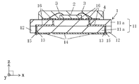
本実施形態における配線基板1は、主面および側面に開口する切欠き部12を有している絶縁基板11と、切欠き部12の内面に位置した内面電極13と、絶縁基板11の主面に位置した外部電極14とを有している。また、絶縁基板11の表面および内部には、配線導体16が位置している。配線基板1は、内面電極13と外部電極14とが接続された接続部15を有している。接続部15の厚みは、内面電極13の厚みおよび外部電極14の厚みより大きくなっている。図1〜図6において、電子装置は仮想のxyz空間におけるxy平面に実装されている。図1〜図6において、上方向とは、仮想のz軸の正方向のことをいう。なお、以下の説明における上下の区別は便宜的なものであり、実際に配線基板1等が使用される際の上下を限定するものではない。
The
なお、図1(b)および図3(a)に示す例において、内面電極13の側面が、平面透視において、接続部15と重なる領域を破線にて示している。
In the examples shown in FIGS. 1 (b) and 3 (a), the region where the side surface of the
絶縁基板11は、一方主面(図1〜図6では下面)および他方主面(図1〜図6では上面)と、側面とを有している。絶縁基板11は、複数の絶縁層11aからなり、主面および側面に開口する切欠き部12を有している。絶縁基板11は電子部品2を支持するための支持体として機能し、絶縁基板11の主面に、電子部品2がはんだバンプ、金バンプまたは導電性樹脂(異方性導電樹脂等)、樹脂等の接続部材を介して接着されて固定される。
The
絶縁基板11は、例えば、酸化アルミニウム質焼結体(アルミナセラミックス),窒化アルミニウム質焼結体,ムライト質焼結体またはガラスセラミックス焼結体等のセラミックスを用いることができる。絶縁基板111は、例えば酸化アルミニウム質焼結体である場合であれば、酸化アルミニウム(Al2O3),酸化珪素(SiO2),酸化マグネシウム(MgO),酸化カルシウム(CaO)等の原料粉末に適当な有機バインダーおよび溶剤等を添加混合して泥漿物を作製する。この泥漿物を、従来周知のドクターブレード法またはカレンダーロール法等を採用してシート状に成形することによってセラミックグリーンシートを作製する。次に、このセラミックグリーンシートに適当な打ち抜き加工を施すとともに、セラミックグリーンシートを必要に応じて複数枚積層して生成形体を形成し、この生成形体を高温(約1600℃)で焼成することによって複数の絶縁層11aからなる絶縁基板11が製作される。As the
絶縁基板11は、図1〜図6に示す例において、2層の絶縁層11aから形成されている。切欠き部12は、絶縁基板11の2層の絶縁層11aのうち、一方主面側の絶縁層11aに形成されている。切欠き部12は、絶縁基板11の主面および側面に開口している。切欠き部12は、図1〜図4に示す例において、絶縁基板11の一方主面と側面とに開口しており、平面視において、角部が円弧状で矩形状に形成された柱状を分断した形状をしている。切欠き部12は、内面に内面電極13が形成されている。切欠き部12は、平面視において半円形状、半楕円形状または半長円形状、あるいは複数の大きさの切欠きが重なった柱状を分断した形状であっても構わない。切欠き部12は、図1に示す例において、絶縁基板11の対向する2つの側面に開口してそれぞれ設けられており、切欠き部12が相対している。
The
切欠き部12は、例えば、絶縁基板11用のセラミックグリーンシートのいくつかにレーザー加工や金型による打ち抜き加工等によって、切欠き部12となる貫通孔をそれぞれのセラミックグリーンシートに形成しておくことにより形成できる。図1〜図4に示す例のように、絶縁基板11の一方主面および側面に開口している切欠き部12は、上記セラミックグリーンシートと、貫通孔を形成していない他のセラミックグリーンシートとを積層することで形成できる。
In the
絶縁基板11の表面および内部には、内面電極13と、外部電極14と、接続部15と、配線導体16とが設けられている。内面電極13は、切欠き部12の内面に位置している。外部電極14は、絶縁基板11の一方主面に位置している。内面電極13と外部電極14とは、切欠き部12の開口に位置している接続部15にて接続している。接続部15は、内面電極13の下面と内面電極13の側面端面とを覆うように位置している。配線導体16は、絶縁基板11の表面および内部に設けられており、絶縁層11aの表面に設けられた配線層と、絶縁層11aの厚み方向(図1〜図6ではz方向)に設けられた貫通導体とを有している。配線導体16の一端部は、図1および図2に示す例において、絶縁基板11の他方主面に導出しており、配線導体16の他端部は、切欠き部12の奥底部にて内面電極13に接続している。内面電極13と、外部電極14と、接続部15と、配線導体16とは、電子部品2とモジュール用基板5とを電気的に接続するためのものである。
An
接続部15の厚みT3は、内面電極13の厚みT1および外部電極14の厚みT2より大きくなっている(T3>T1、T3>T2)。なお、内面電極13の厚みT1とは、切欠き部12の内面から内面電極13の表面までの厚みである。外部電極14の厚みT2とは、絶縁基板11の主面から外部電極14の表面までの厚みである。接続部15の厚みT3とは、切欠き部12の内面または絶縁基板11の主面から接続部15の表面までの厚みである。接続部15の厚みT3は、1.1T1≦T3≦3T1、かつ1.1T2≦T3≦3T2程度に形成される。
The thickness T3 of the connecting
内面電極13、外部電極14、接続部15、配線導体16は、例えばタングステン(W),モリブデン(Mo),マンガン(Mn),銀(Ag)または銅(Cu)等を主成分とする金属粉末メタライズである。例えば、絶縁基板11が酸化アルミニウム質焼結体から成る場合であれば、W,MoまたはMn等の高融点金属粉末に適当な有機バインダーおよび溶媒等を添加混合して得たメタライズペーストを、絶縁基板11用のセラミックグリーンシートに予めスクリーン印刷法等によって所定のパターンに印刷塗布して、絶縁基板11用のセラミックグリーンシートと同時に焼成することによって、絶縁基板11の所定位置に被着形成される。内面電極13および接続部15は、絶縁基板11用のセラミックグリーンシートに形成された切欠き部12用の貫通孔の内面に、内面電極13用のメタライズペーストをスクリーン印刷法等の印刷手段によって印刷塗布し、絶縁基板11用のセラミックグリーンシートとともに焼成することによって形成される。外部電極14、接続部15、配線導体16の配線層は、絶縁基板11用のセラミックグリーンシートの表面に、外部電極14、接続部15、配線導体16の配線層用のメタライズペーストをスクリーン印刷法等の印刷手段によって印刷塗布し、絶縁基板11用のセラミックグリーンシートとともに焼成することによって形成される。配線導体16が貫通導体である場合、貫通導体は、例えば、絶縁基板11用のセラミックグリーンシートに金型またはパンチングによる打ち抜き加工またはレーザー加工等の加工方法によって貫通導体用の貫通孔を形成し、この貫通孔に貫通導体用のメタライズペーストを上記印刷手段によって充填しておき、絶縁基板11用のセラミックグリーンシートとともに焼成することによって形成される。メタライズペーストは、上述の金属粉末に適当な溶剤およびバインダーを加えて混練することによって、適度な粘度に調整して作製される。なお、絶縁基板11との接合強度を高めるために、ガラス粉末、セラミック粉末を含んでいても構わない。
The
内面電極13、外部電極14、接続部15、配線導体16の絶縁基板11から露出する表面には、電気めっき法または無電解めっき法によって金属めっき層が被着される。金属めっき層は、ニッケル,銅,金または銀等の耐食性および接続部材3との接続性に優れる金属から成るものであり、例えば厚さ0.5〜5μm程度のニッケルめっき層と0.1〜3μm程度の金めっき層とが順次被着される。これによって、内面電極13、外部電極14、接続部15、配線導体16が腐食することを効果的に抑制できるとともに、配線導体16と電子部品2との接合、配線導体16とボンディングワイヤ等の接続部材3との接合、ならびに内面電極13、外部電極14、接続部15とモジュール用基板5に形成された接続用の接続パッド51との接合を強固にできる。
A metal plating layer is adhered to the surface exposed from the insulating
また、金属めっき層は、ニッケルめっき層/金めっき層に限られるものではなく、ニッケルめっき層/パラジウムめっき層/金めっき層等を含むその他の金属めっき層であっても構わない。 Further, the metal plating layer is not limited to the nickel plating layer / gold plating layer, and may be another metal plating layer including a nickel plating layer / palladium plating layer / gold plating layer and the like.
配線基板1の搭載部に電子部品2を搭載し、電子装置を作製できる。配線基板1に搭載される電子部品2は、ICチップまたはLSIチップ等の半導体素子,発光素子,水晶振動子または圧電振動子等の圧電素子および各種センサ等である。例えば、電子部品2がワイヤボンディング型の半導体素子である場合には、半導体素子は、低融点ろう材または導電性樹脂等の接合部材によって、搭載部上に固定された後、ボンディングワイヤ等の接続部材3を介して半導体素子の電極と配線導体16とが電気的に接続されることによって配線基板1に搭載される。これにより、電子部品2は配線導体16に電気的に接続される。また、例えば電子部品2がフリップチップ型の半導体素子である場合には、半導体素子は、はんだバンプ、金バンプまたは導電性樹脂(異方性導電樹脂等)等の接続部材3を介して、半導体素子の電極と配線導体16とが電気的および機械的に接続されることによって配線基板1に搭載される。また、配線基板1には、複数の電子部品2を搭載してもよいし、必要に応じて、抵抗素子または容量素子等の小型の電子部品を搭載してもよい。また、電子部品2は必要に応じて、樹脂またはガラス等からなる封止材4を用いて、樹脂、ガラス、セラミックスまたは金属等からなる蓋体等により封止される。
An electronic device can be manufactured by mounting an
本実施形態の電子装置の外部電極14が、例えば、図6に示すように、モジュール用基板5の接続パッド51にはんだ6を介して接続されて、電子モジュールとなる。電子装置は、例えば、図6に示すように、配線基板1の上面側に位置した外部電極14が、モジュール用基板5の接続パッド51に接続されている。
As shown in FIG. 6, for example, the
本実施形態の配線基板1は、主面および側面に開口する切欠き部12を有している絶縁基板11と、切欠き部12の内面に位置した内面電極13と、絶縁基板11の主面に位置した外部電極14とを含んでおり、内面電極13と外部電極14とが接続された接続部15を有しており、接続部1の厚みは、内面電極13の厚みおよび外部電極14の厚みより大きくなっていると、配線基板1とモジュール用基板5とを接合した際に、内面電極13と外部電極14との境界の接続部15において肉厚にすることで、配線基板1の平面方向と直交する方向に対するはんだ6との係止部を有する構成となり配線基板1とモジュール用基板5との接続信頼性を高め、内面電極13と外部電極14との境界の接続部15において放熱しやすくすることができる。
The
電子部品2として発光素子を用いる場合、配線基板1とモジュール用基板5との接続信頼性を高めるとともに、内面電極13と外部電極14との境界の接続部15において放熱しやすくし、輝度に優れた発光装置用の配線基板1とすることができる。
When a light emitting element is used as the
また、接続部15は、図1および図2に示す例のように、絶縁基板11の相対する2辺に、互いに相対するように位置していると、配線基板1とモジュール用基板5との接続信頼性を良好に高め、内面電極13と外部電極14との境界の接続部15において良好に放熱しやすくすることができる。なお、この構成は後述する第2〜5の実施形態における配線基板1においても適用することができる。
Further, when the connecting
また、接続部15は、図1〜図4に示す例のように、切欠き部12における主面側の開口に沿って位置していると、配線基板1の平面方向と直交する方向に対するはんだ6との係止部を切欠き部12の開口に沿って有する構成となりより良好に配線基板1とモジュール用基板5との接続信頼性を高め、切欠き部12の開口に沿って内面電極13と外部電極14との境界の接続部15においてより良好に放熱しやすくすることができる。なお、この構成は後述する第2〜5の実施形態における配線基板1においても適用することができる。
Further, when the connecting
さらに、接続部15は、切欠き部12の内面に沿った方向における、内面電極13の幅と同等の長さを有していると、配線基板1の平面方向と直交する方向に対するはんだ6との係止部を内面電極13の幅全体にわたって有する構成となりより良好に配線基板1とモジュール用基板5との接続信頼性を高め、内面電極13の幅全体にわたって内面電極13と外部電極14との境界の接続部15においてより良好に放熱しやすくすることができる。なお、この構成は後述する第2〜5の実施形態における配線基板1においても適用することができる。
Further, if the connecting
なお、接続部15は、図2に示す例のように、絶縁基板11の主面に沿った方向において、厚みが大きくなっていると、配線基板1の平面方向と直交する方向に対するはんだ6との係止部を有する構成となりより良好に接続信頼性を高め、内面電極13と外部電極14との境界の接続部15により良好に放熱しやすくすることができる。なお、この構成は後述する第2〜5の実施形態における配線基板1においても適用することができる。
As shown in the example shown in FIG. 2, when the thickness of the connecting
また、図2および図3(b)に示す例のように、接続部15は、絶縁基板11の主面に沿った方向に厚くなり、切欠き部12に露出した側面が凸曲面状であると、内面電極13と外部電極14との境界の接続部15全体にわたってはんだ6を濡れ広がらせて接着しやすくし、配線基板1の平面方向と直交する方向に対するはんだ6との係止部を有する構成となり、より良好に接続信頼性を高め、内面電極13と外部電極14との境界の接続部15により良好に放熱しやすくすることができる。なお、この構成は後述する第2〜5の実施形態における配線基板1においても適用することができる。なお、接続部15は、絶縁基板11の主面に沿った方向に厚くなり、切欠き部12に露出した側面が、切欠き部12における主面側の開口に沿って凸曲面状であると、切欠き部12の開口に沿って内面電極13と外部電極14との境界の接続部15全体にわたって濡れ広がらせて接着しやすくすることができる。
Further, as shown in the examples shown in FIGS. 2 and 3B, the connecting
第1の実施形態における配線基板1は、例えば、以下の製造方法により製作することができる。
The
第1の製造方法は、図5(a)に示された例のように、絶縁基板11となるセラミックグリーンシート111に配線導体16用の貫通孔112を形成する。また、絶縁基板11となるセラミックグリーンシート211の表面に、切欠き部12用の貫通孔212を形成する。そして、図5(b)に示された例のように、絶縁基板11となるセラミックグリーンシート111の配線導体16用の貫通孔112に配線導体16用の導体ペースト116を充填する。また、セラミックグリーンシート211の切欠き部12となる貫通孔212の内面に、内面電極13用の導体ペースト113をスクリーン印刷法によって塗布印刷する。そして、図5(c)に示す例のように、絶縁基板11となるセラミックグリーンシート111の表面に配線導体16用の導体ペースト116を印刷塗布する。また、絶縁基板11となるセラミックグリーンシート211の表面に外部電極14用の導体ペースト114と配線導体16用の導体ペースト116とを印刷塗布し、それぞれの導体ペーストと内面電極13用の導体ペースト113とを接続する。この際、外部電極14用の導体ペースト114の端部が内面電極13用の導体ペースト113の表面と重なるように、外部電極14用の導体ペースト114を切欠き部12となる貫通孔212の内面に延出させて印刷塗布する。そして、セラミックグリーンシート111とセラミックグリーンシート211とを積層して加圧することにより、内面電極13用の導体ペースト113と外部電極14用の導体ペースト114との接続部において、内面電極13用の導体ペースト113の厚みが厚い絶縁基板11となるセラミック生積層体を形成し、このセラミック生積層体を焼成することにより、図5(d)に示す例のように、接続部15の厚みが、内面電極13の厚みおよび外部電極14の厚みより大きい凹部312を有する絶縁基板11を形成する。さらに、図5(e)に示された例のように、凹部312を分断することにより、切欠き部12の内側面に位置し、内面電極13と外部電極14との接続部15の厚みが、内面電極13の厚みおよび外部電極14の厚みより大きい配線基板1を製作することができる。
In the first manufacturing method, as in the example shown in FIG. 5A, a through
本開示の電子装置によれば、上記構成の配線基板と、配線基板に搭載された電子部品とを有していることによって、長期信頼性に優れた電子装置とすることができる。 According to the electronic device of the present disclosure, it is possible to obtain an electronic device having excellent long-term reliability by having the wiring board having the above configuration and the electronic components mounted on the wiring board.
本開示の電子モジュールによれば、接続パッドを有するモジュール用基板と、接続パッドにはんだを介して接続された上記構成の電子装置とを有していることによって、長期信頼性に優れたものとすることができる。 According to the electronic module of the present disclosure, long-term reliability is excellent by having a module board having a connection pad and an electronic device having the above configuration connected to the connection pad via solder. can do.
本実施形態における配線基板1は、小型の電子装置において好適に使用することができる。電子部品2が発光素子である場合、高輝度の発光装置用の配線基板1として好適に使用することができる。
The
(第2の実施形態)
次に、第2の実施形態による電子装置について、図7〜図11を参照しつつ説明する。(Second embodiment)
Next, the electronic device according to the second embodiment will be described with reference to FIGS. 7 to 11.
第2の実施形態における電子装置において、上述の第1の実施形態の電子装置と異なる点は、接続部15が、絶縁基板11の厚み方向(図7〜図11ではz方向)において、厚みが大きくなっている点である。なお、第2の実施形態における切欠き部12は、図7に示す例のように、複数の大きさの切欠きが重なった柱状または錐台を分断した形状である。なお、図7(b)および図9(a)に示す例において、内面電極13の側面が、平面透視において、接続部15と重なる領域を破線にて示している。第2の実施形態の配線基板1の絶縁基板11は、図7〜図11に示す例において、2層の絶縁層11aから形成されている。切欠き部12は、絶縁基板11の2層の絶縁層11aのうち、一方主面(図7〜図11では下面)側の絶縁層11aに形成されている。
The difference between the electronic device of the second embodiment and the electronic device of the first embodiment described above is that the connecting
第2の実施形態の配線基板1の接続部15の厚みT3は、第1の実施形態の配線基板1と同様に、内面電極13の厚みT1および外部電極14の厚みT2より大きくなっている(T3>T1、T3>T2)。接続部15の厚みT3は、1.1T1≦T3≦3T1、かつ1.1T2≦T3≦3T2程度に形成される。
The thickness T3 of the
第2の実施形態における配線基板1は、接続部15が、絶縁基板11の厚み方向において、厚みが大きくなっており、配線基板1の厚み方向と直交する方向に対するはんだ6との係止部を有する構成となり、より良好に配線基板1とモジュール用基板5との接続信頼性を高め、内面電極13と外部電極14との境界の接続部15により良好に放熱しやすくすることができる。
In the
また、配線基板1とモジュール用基板5との間を大きくし、はんだ6を多く配設し、配線基板1とモジュール用基板5との接続信頼性を高めるとともに、内面電極13と外部電極14との境界の接続部15により良好に放熱しやすくすることができる。
Further, the space between the
また、図8および図9に示す例のように、絶縁基板11の厚み方向において、厚みが大きくなっている接続部15が、絶縁基板11の相対する2辺に、相対するように位置していると、配線基板1とモジュール用基板5との接合する際の傾きを低減し、電子部品2として発光素子を用いる場合、視認性および輝度に優れた発光装置用の配線基板1とすることができる。なお、この構成は後述する第3〜5の実施形態における配線基板1においても適用することができる。
Further, as in the examples shown in FIGS. 8 and 9, in the thickness direction of the insulating
また、図8および図9(b)に示す例のように、接続部15は、絶縁基板11の厚み方向に厚くなり、接続部15の下面が凸曲面状であると、内面電極13と外部電極14との境界の接続部15全体にわたってはんだ6を濡れ広がらせて接着しやすくし、配線基板1の厚み方向と直交する方向に対するはんだ6との係止部を有する構成となり、より良好に接続信頼性を高め、内面電極13と外部電極14との境界の接続部15により良好に放熱しやすくすることができる。なお、この構成は後述する第3〜5の実施形態における配線基板1においても適用することができる。
Further, as shown in the examples shown in FIGS. 8 and 9B, when the connecting
なお、接続部15は、絶縁基板11の主面に沿った方向に厚くなり、接続部15の下面が、切欠き部12における主面側の開口に沿って凸曲面状であると、切欠き部12の開口に沿って内面電極13と外部電極14との境界の接続部15全体にわたって濡れ広がらせて接着しやすくすることができる。
If the connecting
第2の実施形態における配線基板1は、例えば、以下の製造方法により製作することができる。
The
第2の製造方法は、図11(a)に示された例のように、絶縁基板11となるセラミックグリーンシート111に配線導体16用の貫通孔112を形成する。また、絶縁基板11となるセラミックグリーンシート211の表面に、切欠き部12用の貫通孔212を形成する。そして、図11(b)に示された例のように、絶縁基板11となるセラミックグリーンシート111の配線導体16用の貫通孔111に配線導体16用の導体ペースト116を充填する。また、セラミックグリーンシート211の切欠き部12となる貫通孔212の内面に、内面電極13用の導体ペースト113をスクリーン印刷法によって塗布印刷する。この際、内面電極13用の導体ペーストの端部を、セラミックグリーンシート211の表面に延出するように印刷塗布する。そして、図11(c)に示す例のように、絶縁基板11となるセラミックグリーンシート111の表面に配線導体16用の導体ペースト116を印刷塗布する。また、絶縁基板11となるセラミックグリーンシート211の表面に外部電極14用の導体ペースト114と配線導体16用の導体ペースト116とを印刷塗布し、それぞれの導体ペーストと内面電極13用の導体ペースト113とを接続する。この際、外部電極14用の導体ペースト114の端部が、セラミックグリーンシート211の表面に延出した内面電極13用の導体ペースト113の表面と重なるように印刷塗布する。そして、セラミックグリーンシート111とセラミックグリーンシート211とを積層して加圧することにより、内面電極13用の導体ペースト113と外部電極14用の導体ペースト114との接続部において、外部電極14用の導体ペースト114の厚みが厚い絶縁基板11となるセラミック生積層体を形成し、このセラミック生積層体を焼成することにより、図11(d)に示す例のように、接続部15の厚みが、内面電極13の厚みおよび外部電極14の厚みより大きい凹部312を有する絶縁基板11を形成する。さらに、図11(e)に示された例のように、凹部312を分断することにより、切欠き部12の内側面に位置し、内面電極13と外部電極14との接続部15の厚みが、内面電極13の厚みおよび外部電極14の厚みより大きい配線基板1を製作することができる。
In the second manufacturing method, as in the example shown in FIG. 11A, a through
第2の実施形態の配線基板1は、その他においては、上述の第1の実施形態の配線基板1と同様の製造方法を用いて製作することができる。
The
(第3の実施形態)
次に、第3の実施形態による電子装置について、図12〜図16を参照しつつ説明する。なお、図12(b)に示す例において、内面電極13が、平面透視において、接続部15と重なる領域を破線にて示している。(Third Embodiment)
Next, the electronic device according to the third embodiment will be described with reference to FIGS. 12 to 16. In the example shown in FIG. 12B, the region where the
第3の実施形態における電子装置において、上述の実施形態の電子装置と異なる点は、接続部15は、絶縁基板11の主面に沿った方向(図12〜図16ではxy平面方向)および絶縁基板11の厚み方向(図12〜図16ではz方向)において、厚みが大きくなっている点である。なお、図12(b)および図14(a)に示す例において、内面電極13の側面が、平面透視において、接続部15と重なる領域を破線にて示している。第3の実施形態の配線基板1の絶縁基板11は、図12〜図16に示す例において、2層の絶縁層11aから形成されている。切欠き部12は、絶縁基板11の2層の絶縁層11aのうち、一方主面(図12〜図16では下面)側の絶縁層11aに形成されている。
The difference between the electronic device of the third embodiment and the electronic device of the above-described embodiment is that the
第3の実施形態の配線基板1の接続部15の厚みT3は、上述の実施形態の配線基板1と同様に、内面電極13の厚みT1および外部電極14の厚みT2より大きくなっている(T3>T1、T3>T2)。接続部15の厚みT3は、1.1T1≦T3≦3T1、かつ1.1T2≦T3≦3T2程度に形成される。
The thickness T3 of the
第3の実施形態における配線基板1は、接続部15が絶縁基板11の主面に沿った方向および絶縁基板11の厚み方向において、厚みが大きくなっていることにより、配線基板1の平面方向および厚み方向のそれぞれに直交する両方向に対するはんだ6との係止部を有する構成となりより良好に配線基板1とモジュール用基板5との接続信頼性をより効果的に高め、内面電極13と外部電極14との境界の接続部15により良好に放熱しやすくすることができる。
The
なお、接続部15は、絶縁基板11の主面に沿った方向から絶縁基板11の厚み方向にかけて、厚みが大きくなっていると、配線基板1の平面方向から厚み方向にかけて、直交する方向に対するはんだ6との係止部を有する構成となり、より効果的に配線基板1とモジュール用基板5との接続信頼性を高めるとともに、内面電極13と外部電極14との境界の接続部15により良好に放熱しやすくすることができる。
When the thickness of the connecting
また、図13および図14(b)に示す例のように、接続部15は、絶縁基板11の主面に沿った方向および絶縁基板11の厚み方向において厚くなり、接続部15の切欠き部12に露出した側面および下面が凸曲面状であると、内面電極13と外部電極14との境界の接続部15全体にわたってはんだ6を濡れ広がらせて接着しやすくし、配線基板1の平面方向および厚み方向のそれぞれに直交する両方向に対するはんだ6との係止部を有する構成となり、より良好に接続信頼性を高め、内面電極13と外部電極14との境界の接続部15により良好に放熱しやすくすることができる。なお、この構成は後述する第3〜5の実施形態における配線基板1においても適用することができる。
Further, as shown in the examples shown in FIGS. 13 and 14 (b), the connecting
なお、接続部15は、絶縁基板11の主面に沿った方向および絶縁基板11の厚み方向において厚くなり、接続部15の切欠き部12に露出した側面および下面が、切欠き部12における主面側の開口に沿って凸曲面状であると、切欠き部12の開口に沿って内面電極13と外部電極14との境界の接続部15全体にわたって濡れ広がらせて接着しやすくすることができる。
The connecting
第3の実施形態における配線基板1は、例えば、以下の製造方法により製作することができる。
The
第3の製造方法は、図16(a)に示された例のように、絶縁基板11となるセラミックグリーンシート111に配線導体16用の貫通孔112を形成する。また、絶縁基板11となるセラミックグリーンシート211の表面に、切欠き部12用の貫通孔212を形成する。そして、図16(b)に示された例のように、絶縁基板11となるセラミックグリーンシート111の配線導体16用の貫通孔111に配線導体16用の導体ペースト116を充填する。また、セラミックグリーンシート211の切欠き部12となる貫通孔212の内面に、内面電極13用の導体ペースト113をスクリーン印刷法によって塗布印刷する。この際、内面電極13用の導体ペースト113の端部を、セラミックグリーンシート211の表面に延出するように印刷塗布する。そして、図16(c)に示す例のように、絶縁基板11となるセラミックグリーンシート111の表面に配線導体16用の導体ペースト116を印刷塗布する。また、絶縁基板11となるセラミックグリーンシート211の表面に外部電極14用の導体ペースト114と配線導体16用の導体ペースト116とを印刷塗布し、それぞれの導体ペーストと内面電極13用の導体ペースト113とを接続する。この際、外部電極14用の導体ペースト114を外部電極14用の導体ペースト114を切欠き部12となる貫通孔212の内面に延出させて印刷塗布することで、セラミックグリーンシート211の表面側と切欠き部12用の貫通孔212の内面とで、内面電極13用の導体ペーストと外部電極14の導体ペーストとをそれぞれ重ねる。そして、セラミックグリーンシート111とセラミックグリーンシート211とを積層して加圧することにより、内面電極13用の導体ペースト113と配線導体16用の導体ペースト114との接続部において、内面電極13用の導体ペースト113および外部電極14用の導体ペースト114の厚みが厚い絶縁基板11となるセラミック生積層体を形成し、このセラミック生積層体を焼成することにより、図15(d)に示す例のように、接続部15の厚みが、内面電極13の厚みおよび外部電極14の厚みより大きい凹部312を有する絶縁基板11を形成する。さらに、図16(e)に示された例のように、凹部312を分断することにより、切欠き部12の内側面に位置し、内面電極13と外部電極14との接続部15の厚みが、内面電極13の厚みおよび外部電極14の厚みより大きい配線基板1を製作することができる。
In the third manufacturing method, as in the example shown in FIG. 16A, a through
第3の実施形態の配線基板1は、その他においては、上述の実施形態の配線基板1と同様の製造方法を用いて製作することができる。
The
(第4の実施形態)
次に、第4の実施形態による電子装置について、図17および図18を参照しつつ説明する。第4の実施形態における電子装置において、上述の実施形態の電子装置と異なる点は、切欠き部12が、絶縁基板11の両主面および側面に開口している点である。また、絶縁基板11は、他方主面(図17および図18では上面)に、凹部17を有している。なお、図17(b)に示す例において、内面電極13の側面が、平面透視において、接続部15と重なる領域を破線にて示している。(Fourth Embodiment)
Next, the electronic device according to the fourth embodiment will be described with reference to FIGS. 17 and 18. The electronic device of the fourth embodiment is different from the electronic device of the above-described embodiment in that the
第4の実施形態の配線基板1の接続部15の厚みT3は、上述の実施形態の配線基板1と同様に、内面電極13の厚みT1および外部電極14の厚みT2より大きくなっている(T3>T1、T3>T2)。接続部15の厚みT3は、1.1T1≦T3≦3T1、かつ1.1T2≦T3≦3T2程度に形成される。
The thickness T3 of the
第4の実施形態における配線基板1は、第3の実施形態の配線基板1と同様に、配線基板1とモジュール用基板5とを接合した際に、内面電極13と外部電極14との境界の接続部15において肉厚にすることで、配線基板1の平面方向および厚み方向のそれぞれに直交する両方向に対するはんだ6との係止部を有する構成となり配線基板1とモジュール用基板5との接続信頼性をより効果的に高め、内面電極13と外部電極14との境界の接続部15において放熱しやすくすることができる。
Similar to the
また、接続部15は、絶縁基板11の主面に沿った方向から絶縁基板11の厚み方向にかけて、厚みが大きくなっており、配線基板1の平面方向から厚み方向にかけて、直交する方向に対するはんだ6との係止部を有する構成となり、より効果的に配線基板1とモジュール用基板5との接続信頼性を高めるとともに、内面電極13と外部電極14との境界の接続部15により良好に放熱しやすくすることができる。
Further, the connecting
凹部17は、例えば、底面に電子部品2を搭載するためのものである。凹部17の底面には、電子部品2と電気的に接続するための配線導体16が導出している。凹部17は、平面視において、角部が円弧状の矩形状であり、絶縁基板11の中央部に位置している。図17および図18に示す例において、絶縁基板11は、3層の絶縁層11aから形成されており、凹部17は、一方主面側の1番目〜2番目の絶縁層11aに位置している。
The
凹部17は、例えば、絶縁基板11用のセラミックグリーンシートのいくつかにレーザー加工や金型による打ち抜き加工等によって、凹部17となる貫通孔をそれぞれのセラミックグリーンシートに形成し、このセラミックグリーンシートを、貫通孔を形成していない他のセラミックグリーンシートに積層することで形成できる。
The
第4の実施形態の配線基板1は、上述の実施形態の配線基板1と同様の製造方法を用いて製作することができる。
The
(第5の実施形態)
次に、第5の実施形態による電子装置について、図19および図20を参照しつつ説明する。第5の実施形態における電子装置において、上記した第1の実施形態の電子装置と異なる点は、絶縁基板11の内部に、絶縁基板11の厚み方向に沿って形成された外部電極14と配線導体16とを接続するビア18を有する点である。なお、図19(b)に示す例において、内面電極13の側面が、平面透視において、接続部15と重なる領域を破線にて示している。また、図19(b)に示す例において、ビア18の側面が、平面透視において、外部電極14と重なる領域を破線にて示している。(Fifth Embodiment)
Next, the electronic device according to the fifth embodiment will be described with reference to FIGS. 19 and 20. The electronic device according to the fifth embodiment differs from the electronic device according to the first embodiment described above in that the
第5の実施形態の配線基板1の接続部15の厚みT3は、上述の実施形態の配線基板1と同様に、内面電極13の厚みT1および外部電極14の厚みT2より大きくなっている(T3>T1、T3>T2)。接続部15の厚みT3は、1.1T1≦T3≦3T1、かつ1.1T2≦T3≦3T2程度に形成される。
The thickness T3 of the
第5の実施形態における配線基板1は、第3の実施形態の配線基板1と同様に、配線基板1とモジュール用基板5とを接合した際に、内面電極13と外部電極14との境界の接続部15において肉厚にすることで、配線基板1の平面方向および厚み方向の直交する両方向に対するはんだ6との係止部を有する構成となり配線基板1とモジュール用基板5との接続信頼性をより効果的に高め、内面電極13と外部電極14との境界の接続部15において放熱しやすくすることができる。
Similar to the
また、接続部15は、絶縁基板11の主面に沿った方向から絶縁基板11の厚み方向にかけて、厚みが大きくなっており、配線基板1の平面方向から厚み方向にかけて、直交する方向に対するはんだ6との係止部を有する構成となり、より効果的に配線基板1とモジュール用基板5との接続信頼性を高めるとともに、内面電極13と外部電極14との境界の接続部15により良好に放熱しやすくすることができる。
Further, the connecting
また、図19および図20に示す例において、1つの外部電極14に1つのビア18が接続されているが、1つの外部電極14に複数のビア18が接続されている配線基板1であっても構わない。
Further, in the examples shown in FIGS. 19 and 20, one via 18 is connected to one
ビア18は、配線導体16の貫通導体と同様の製造方法により製作することができる。
The via 18 can be manufactured by the same manufacturing method as the through conductor of the
第5の実施形態の配線基板1は、上述の実施形態の配線基板1と同様の製造方法を用いて製作することができる。
The
本開示は、上述の実施の形態の例に限定されるものではなく、種々の変更は可能である。例えば、絶縁基板11は、平面視において、側面または角部に切欠き部や面取り部を有している矩形状であっても構わない。
The present disclosure is not limited to the examples of the embodiments described above, and various modifications can be made. For example, the insulating
また、上述の実施形態の配線基板1において、絶縁基板11の下面側に、外部電極14が形成しているが、絶縁基板11の上面側、すなわち、電子部品2の搭載部と同じ主面側にて、外部電極14を有するものであっても構わない。
Further, in the
また、第1〜第5の実施形態の配線基板1の構成を組み合わせても構わない。例えば、第1の実施形態の配線基板1または第3〜第5の実施形態の配線基板1において、配線基板1が、凹部17を有しているものであって構わない。また、第1〜第4の実施形態の配線基板1において、ビア18を備えていても構わない。
Further, the configurations of the
また、上述の実施形態において、切欠き部12、内面電極13、外部電極14、接続部15は、絶縁基板11の相対する2辺に位置しているが、例えば、絶縁基板11が矩形状の場合、絶縁基板11の4辺に、互いに位置していても構わない。
Further, in the above-described embodiment, the
また、接続部15が絶縁基板11の厚み方向において、厚みが大きくなっている配線基板1において、外部電極14の表面に、接続部15と同等の大きさ(≒T3)に周囲の領域よりも部分的に厚くなる領域を有しておいても良い。これにより、配線基板1とモジュール用基板5との接合する際の傾きをより低減し、電子部品2として発光素子を用いる場合、視認性および輝度に優れた発光装置用の配線基板1とすることができる。例えば、第5の実施形態の配線基板1において、平面視にてビア18と重なる外部電極14の表面を、周囲の外部電極14よりも厚くなるようにしておくとよい。
Further, in the
上述の実施形態において、絶縁基板11は、2層または3層の絶縁層11aにより構成している例を示しているが、絶縁基板11は、4層以上の絶縁層11aにより構成していても構わない。
In the above-described embodiment, the insulating
また、配線基板1は、多数個取り配線基板の形態で製作されていてもよい。
Further, the
Claims (8)
前記切欠き部の内面に位置し、前記主面に延出した内面電極と、
前記絶縁基板の主面から前記内面電極の側面にかけて位置した外部電極とを含んでおり、前記内面電極と前記外部電極とが接続された接続部を有しており、
該接続部の厚みは、前記内面電極の厚みおよび前記外部電極の厚みより大きく、
前記接続部において、前記外部電極は、前記内面電極の側面を覆っており、前記絶縁基板の厚み方向における、前記外部電極の長さは、延出した前記内面電極の長さより大きいことを特徴とする配線基板。 Insulated substrates with notches that open on the main and side surfaces,
An inner electrode located on the inner surface of the notch and extending to the main surface,
It includes an external electrode located from the main surface of the insulating substrate to the side surface of the inner surface electrode, and has a connecting portion in which the inner surface electrode and the outer electrode are connected.
The thickness of the connection portion is larger than the thickness of the inner surface electrode and the thickness of the outer electrode.
In the connection portion, the external electrode covers the side surface of the inner surface electrode, and the length of the external electrode in the thickness direction of the insulating substrate is larger than the length of the extended inner surface electrode. Wiring board.
該配線基板に搭載された電子部品とを有することを特徴とする電子装置。 The wiring board according to any one of claims 1 to 6.
An electronic device having an electronic component mounted on the wiring board.
前記接続パッドにはんだを介して接続された請求項7に記載の電子装置とを有することを特徴とする電子モジュール。 Module board with connection pad and
The electronic module according to claim 7, further comprising the electronic device according to claim 7, which is connected to the connection pad via solder.
Priority Applications (2)
| Application Number | Priority Date | Filing Date | Title |
|---|---|---|---|
| JP2021123460A JP7244587B2 (en) | 2016-11-28 | 2021-07-28 | electronic module |
| JP2023036918A JP7554304B2 (en) | 2016-11-28 | 2023-03-09 | Wiring board, electronic device and electronic module |
Applications Claiming Priority (3)
| Application Number | Priority Date | Filing Date | Title |
|---|---|---|---|
| JP2016230215 | 2016-11-28 | ||
| JP2016230215 | 2016-11-28 | ||
| PCT/JP2017/042618 WO2018097313A1 (en) | 2016-11-28 | 2017-11-28 | Wiring board, electronic device, and electronic module |
Related Child Applications (1)
| Application Number | Title | Priority Date | Filing Date |
|---|---|---|---|
| JP2021123460A Division JP7244587B2 (en) | 2016-11-28 | 2021-07-28 | electronic module |
Publications (2)
| Publication Number | Publication Date |
|---|---|
| JPWO2018097313A1 JPWO2018097313A1 (en) | 2019-10-17 |
| JP6923554B2 true JP6923554B2 (en) | 2021-08-18 |
Family
ID=62195122
Family Applications (3)
| Application Number | Title | Priority Date | Filing Date |
|---|---|---|---|
| JP2018553017A Active JP6923554B2 (en) | 2016-11-28 | 2017-11-28 | Wiring boards, electronics and electronic modules |
| JP2021123460A Active JP7244587B2 (en) | 2016-11-28 | 2021-07-28 | electronic module |
| JP2023036918A Active JP7554304B2 (en) | 2016-11-28 | 2023-03-09 | Wiring board, electronic device and electronic module |
Family Applications After (2)
| Application Number | Title | Priority Date | Filing Date |
|---|---|---|---|
| JP2021123460A Active JP7244587B2 (en) | 2016-11-28 | 2021-07-28 | electronic module |
| JP2023036918A Active JP7554304B2 (en) | 2016-11-28 | 2023-03-09 | Wiring board, electronic device and electronic module |
Country Status (5)
| Country | Link |
|---|---|
| US (1) | US11024572B2 (en) |
| EP (1) | EP3547357A4 (en) |
| JP (3) | JP6923554B2 (en) |
| CN (1) | CN109997220B (en) |
| WO (1) | WO2018097313A1 (en) |
Families Citing this family (1)
| Publication number | Priority date | Publication date | Assignee | Title |
|---|---|---|---|---|
| US11910530B2 (en) | 2022-03-25 | 2024-02-20 | Tactotek Oy | Method for manufacturing electronics assembly and electronics assembly |
Family Cites Families (23)
| Publication number | Priority date | Publication date | Assignee | Title |
|---|---|---|---|---|
| US5994648A (en) * | 1997-03-27 | 1999-11-30 | Ford Motor Company | Three-dimensional molded sockets for mechanical and electrical component attachment |
| JP2002158509A (en) | 2000-11-21 | 2002-05-31 | Mitsubishi Electric Corp | High-frequency circuit module and production method therefor |
| US7266869B2 (en) * | 2003-07-30 | 2007-09-11 | Kyocera Corporation | Method for manufacturing a piezoelectric oscillator |
| JP2005159083A (en) | 2003-11-27 | 2005-06-16 | Kyocera Corp | Multiple wiring board |
| JP4424420B2 (en) | 2005-04-18 | 2010-03-03 | 株式会社村田製作所 | Electronic component module |
| JP4436336B2 (en) * | 2006-03-15 | 2010-03-24 | 日本特殊陶業株式会社 | Multi-piece wiring board and manufacturing method thereof |
| WO2009044737A1 (en) | 2007-10-01 | 2009-04-09 | Murata Manufacturing Co., Ltd. | Electronic component |
| WO2010114115A1 (en) * | 2009-04-03 | 2010-10-07 | 株式会社大真空 | Package member assembly, method for manufacturing package member assembly, package member, and method for manufacturing piezoelectric vibration device using package member |
| JPWO2011002031A1 (en) * | 2009-06-30 | 2012-12-13 | 三洋電機株式会社 | Device mounting substrate and semiconductor module |
| WO2011065485A1 (en) * | 2009-11-26 | 2011-06-03 | 京セラ株式会社 | Wiring substrate, imaging device and imaging device module |
| JPWO2012137714A1 (en) * | 2011-04-04 | 2014-07-28 | ローム株式会社 | Semiconductor device and manufacturing method of semiconductor device |
| JP5734434B2 (en) * | 2011-07-25 | 2015-06-17 | 京セラ株式会社 | Wiring board, electronic device and electronic module |
| WO2013180247A1 (en) * | 2012-05-30 | 2013-12-05 | 京セラ株式会社 | Wiring board and electronic device |
| JP6096812B2 (en) | 2013-01-22 | 2017-03-15 | 京セラ株式会社 | Electronic device mounting package, electronic device and imaging module |
| US9609743B2 (en) * | 2013-01-31 | 2017-03-28 | Kyocera Corporation | Electronic device mounting substrate, electronic apparatus, and imaging module |
| CN105359632B (en) * | 2013-10-23 | 2018-02-06 | 京瓷株式会社 | Circuit board and electronic installation |
| JP6224473B2 (en) | 2014-02-03 | 2017-11-01 | 京セラ株式会社 | Wiring board, electronic device and electronic module |
| JP6166194B2 (en) | 2014-02-21 | 2017-07-19 | 京セラ株式会社 | Wiring board, electronic device and electronic module |
| EP3136430B1 (en) * | 2014-04-22 | 2021-06-16 | Kyocera Corporation | Wiring board, electronic device, and electronic module |
| JP6325346B2 (en) | 2014-05-28 | 2018-05-16 | 京セラ株式会社 | Wiring board, electronic device and electronic module |
| CN110943151B (en) | 2015-02-25 | 2023-07-14 | 京瓷株式会社 | Package for mounting light-emitting element, light-emitting device, and light-emitting module |
| JP6408423B2 (en) | 2015-04-24 | 2018-10-17 | 京セラ株式会社 | Package and electronic equipment |
| EP3633719A4 (en) * | 2017-05-26 | 2021-03-17 | Kyocera Corporation | SUBSTRATE FOR THE ASSEMBLY OF ELECTRONIC COMPONENTS, ELECTRONIC DEVICE AND ELECTRONIC MODULE |
-
2017
- 2017-11-28 EP EP17874717.6A patent/EP3547357A4/en active Pending
- 2017-11-28 WO PCT/JP2017/042618 patent/WO2018097313A1/en active Application Filing
- 2017-11-28 CN CN201780071696.9A patent/CN109997220B/en active Active
- 2017-11-28 US US16/463,915 patent/US11024572B2/en active Active
- 2017-11-28 JP JP2018553017A patent/JP6923554B2/en active Active
-
2021
- 2021-07-28 JP JP2021123460A patent/JP7244587B2/en active Active
-
2023
- 2023-03-09 JP JP2023036918A patent/JP7554304B2/en active Active
Also Published As
| Publication number | Publication date |
|---|---|
| JP7554304B2 (en) | 2024-09-19 |
| JPWO2018097313A1 (en) | 2019-10-17 |
| JP2023071984A (en) | 2023-05-23 |
| JP7244587B2 (en) | 2023-03-22 |
| US11024572B2 (en) | 2021-06-01 |
| CN109997220A (en) | 2019-07-09 |
| US20200075472A1 (en) | 2020-03-05 |
| EP3547357A4 (en) | 2020-07-01 |
| CN109997220B (en) | 2023-09-12 |
| WO2018097313A1 (en) | 2018-05-31 |
| JP2021184481A (en) | 2021-12-02 |
| EP3547357A1 (en) | 2019-10-02 |
Similar Documents
| Publication | Publication Date | Title |
|---|---|---|
| US11145587B2 (en) | Electronic component mounting substrate, electronic device, and electronic module | |
| US10334740B2 (en) | Electronic-component mount substrate, electronic device, and electronic module | |
| US10699993B2 (en) | Wiring board, electronic device, and electronic module | |
| JP6767204B2 (en) | Boards for mounting electronic components, electronic devices and electronic modules | |
| JP7554304B2 (en) | Wiring board, electronic device and electronic module | |
| US11004781B2 (en) | Electronic component mounting substrate, electronic device, and electronic module | |
| JP6780996B2 (en) | Wiring boards, electronics and electronic modules | |
| JP6698301B2 (en) | Wiring board, electronic device and electronic module | |
| JP6826185B2 (en) | Wiring boards, electronics and electronic modules | |
| JP6878562B2 (en) | Wiring boards, electronics and electronic modules | |
| JPWO2020137152A1 (en) | Wiring boards, electronics and electronic modules | |
| JP6737646B2 (en) | Wiring board, electronic device and electronic module | |
| CN107431047B (en) | Wiring board, electronic device, and electronic module | |
| JP6595308B2 (en) | Electronic component mounting substrate, electronic device and electronic module | |
| JP2017112270A (en) | Substrate for mounting electronic component, electronic device and electronic module |
Legal Events
| Date | Code | Title | Description |
|---|---|---|---|
| A621 | Written request for application examination |
Free format text: JAPANESE INTERMEDIATE CODE: A621 Effective date: 20190513 |
|
| A131 | Notification of reasons for refusal |
Free format text: JAPANESE INTERMEDIATE CODE: A131 Effective date: 20200428 |
|
| A521 | Request for written amendment filed |
Free format text: JAPANESE INTERMEDIATE CODE: A523 Effective date: 20200625 |
|
| A131 | Notification of reasons for refusal |
Free format text: JAPANESE INTERMEDIATE CODE: A131 Effective date: 20201207 |
|
| A521 | Request for written amendment filed |
Free format text: JAPANESE INTERMEDIATE CODE: A523 Effective date: 20210204 |
|
| TRDD | Decision of grant or rejection written | ||
| A01 | Written decision to grant a patent or to grant a registration (utility model) |
Free format text: JAPANESE INTERMEDIATE CODE: A01 Effective date: 20210629 |
|
| A61 | First payment of annual fees (during grant procedure) |
Free format text: JAPANESE INTERMEDIATE CODE: A61 Effective date: 20210729 |
|
| R150 | Certificate of patent or registration of utility model |
Ref document number: 6923554 Country of ref document: JP Free format text: JAPANESE INTERMEDIATE CODE: R150 |