JP6697328B2 - Wafer detecting method for detecting outer peripheral position of wafer and processing apparatus capable of detecting outer peripheral position of wafer - Google Patents
Wafer detecting method for detecting outer peripheral position of wafer and processing apparatus capable of detecting outer peripheral position of wafer Download PDFInfo
- Publication number
- JP6697328B2 JP6697328B2 JP2016112564A JP2016112564A JP6697328B2 JP 6697328 B2 JP6697328 B2 JP 6697328B2 JP 2016112564 A JP2016112564 A JP 2016112564A JP 2016112564 A JP2016112564 A JP 2016112564A JP 6697328 B2 JP6697328 B2 JP 6697328B2
- Authority
- JP
- Japan
- Prior art keywords
- wafer
- outer peripheral
- light
- slice level
- image
- Prior art date
- Legal status (The legal status is an assumption and is not a legal conclusion. Google has not performed a legal analysis and makes no representation as to the accuracy of the status listed.)
- Active
Links
Images


Landscapes
- Mechanical Treatment Of Semiconductor (AREA)
- Length Measuring Devices By Optical Means (AREA)
- Constituent Portions Of Griding Lathes, Driving, Sensing And Control (AREA)
- Finish Polishing, Edge Sharpening, And Grinding By Specific Grinding Devices (AREA)
Description
本発明は、ウェーハの外周位置を検出するウェーハの検出方法及びウェーハの外周位置を検出することが可能な加工装置に関する。 The present invention relates to a wafer detection method for detecting the outer peripheral position of a wafer and a processing apparatus capable of detecting the outer peripheral position of the wafer.
半導体製造プロセスにおけるウェーハの研削において、例えば外周部分が丸く面取りされたウェーハを研削して薄化すると、ウェーハの外周部は、外周部に向かって尖ったエッジ状に形成される。そして、この尖ったエッジが原因となってウェーハの外周の強度が低下することで、ウェーハの外周に衝撃が加わった際にウェーハが割れやすくなるという問題、所謂ウェーハのシャープエッジの問題がある。このシャープエッジによるウェーハ割れを防ぐために、ウェーハを研削し薄化する前に、ウェーハの外周の面取り部分を切削等により円形状にトリミングし除去することにより、薄化後のウェーハに尖ったエッジが形成されないようにするウェーハの加工方法がある(例えば、特許文献1参照)。 In grinding a wafer in a semiconductor manufacturing process, for example, when a wafer whose outer peripheral portion is rounded and chamfered is ground and thinned, the outer peripheral portion of the wafer is formed in a sharp edge shape toward the outer peripheral portion. Then, the sharp edge causes the strength of the outer periphery of the wafer to decrease, which causes a problem that the wafer is likely to be broken when an impact is applied to the outer periphery of the wafer, that is, a so-called sharp edge of the wafer. In order to prevent wafer cracking due to this sharp edge, before grinding and thinning the wafer, the chamfered portion on the outer periphery of the wafer is trimmed into a circular shape by cutting and removed, so that the sharpened edge on the wafer after thinning There is a wafer processing method for preventing the formation (for example, refer to Patent Document 1).
また、上記特許文献1に記載されているような除去加工を切削ブレードでウェーハに施すための装置がある(例えば、特許文献2参照)。このような装置においては、ウェーハに異物が付着することを防ぐために、例えば、ウェーハは、ウェーハの裏面の外周部分のみを保持する環状保持面を有した保持ユニットで保持された状態で加工される。 In addition, there is an apparatus for performing a removal process on a wafer with a cutting blade as described in Patent Document 1 (see, for example, Patent Document 2). In such an apparatus, in order to prevent foreign matter from adhering to the wafer, for example, the wafer is processed while being held by a holding unit having an annular holding surface that holds only the outer peripheral portion of the back surface of the wafer. ..
そして、ウェーハへ切削ブレードを切り込ませる位置は、例えば特許文献3に開示されているように、撮像手段でウェーハの外周縁領域を撮像して形成した撮像画像から外周縁を検出して決定しており、この撮像画像から検出したウェーハの外周縁から所定距離だけ径方向内側の位置を切削ブレードで周方向に向かって切削している。 Then, the position where the cutting blade is cut into the wafer is determined by detecting the outer peripheral edge from a captured image formed by capturing an image of the outer peripheral edge region of the wafer by the image capturing unit, as disclosed in Patent Document 3, for example. Therefore, a position radially inward from the outer peripheral edge of the wafer detected from this captured image is cut by a cutting blade in the circumferential direction.
しかし、ウェーハを撮像する際の光量や形成された撮像画像の画像処理が適切でない場合には、実際の外周縁位置と異なる位置をウェーハの外周縁として検出してしまうおそれがある。よって、ウェーハの外周縁位置を検出する場合には、実際の外周縁位置と異なる位置をウェーハの外周縁として検出してしまうおそれを低減するという課題がある。 However, if the amount of light at the time of imaging the wafer or the image processing of the formed captured image is not appropriate, a position different from the actual outer peripheral edge position may be detected as the outer peripheral edge of the wafer. Therefore, when detecting the outer peripheral edge position of the wafer, there is a problem of reducing the risk of detecting a position different from the actual outer peripheral edge position as the outer peripheral edge of the wafer.
上記課題を解決するための本発明は、ウェーハを保持する保持面を有した保持テーブルと、該保持テーブルで保持されたウェーハに光を照射する光照射器と該保持テーブルで保持されたウェーハを撮像し撮像画像を形成するカメラとを有した撮像手段と、を備えた装置を用いてウェーハの外周位置を検出するウェーハの検出方法であって、該保持テーブルでウェーハを保持する保持ステップと、該保持ステップを実施した後、該保持テーブルで保持されたウェーハに該光照射器から複数の階層の光量を照射し該カメラで撮像してウェーハの外周縁を含む撮像画像を複数形成する撮像画像形成ステップと、該撮像画像形成ステップを実施した後、複数の階層の光量毎に撮像された該撮像画像をそれぞれ複数の階層のスライスレベルで二値化して二値化画像を形成する二値化ステップと、該二値化ステップで形成された該二値化画像における白い画素と黒い画素との境界をウェーハの外周縁の座標位置として検出し記録するウェーハ外周位置検出ステップと、該ウェーハ外周位置検出ステップで記録された位置座標が最も密集する座標位置の光量とスライスレベルとを最適値として設定する光量スライスレベル設定ステップと、を備えたウェーハの検出方法である。 The present invention for solving the above problems, a holding table having a holding surface for holding the wafer, a light irradiator for irradiating the wafer held by the holding table with light, and a wafer held by the holding table. An image pickup means having a camera for picking up an image to form a picked-up image, and a wafer detection method for detecting the outer peripheral position of the wafer using an apparatus provided with, a holding step of holding the wafer on the holding table, After performing the holding step, the wafer held by the holding table is irradiated with light amounts of a plurality of layers from the light irradiator and is imaged by the camera to form a plurality of imaged images including the outer peripheral edge of the wafer. Binarization for forming a binarized image by performing the forming step and the picked-up image forming step, and then binarizing the picked-up images picked up for each of the light amounts of the plurality of layers at slice levels of the plurality of layers. Step, a wafer outer peripheral position detecting step of detecting and recording the boundary between white pixels and black pixels in the binarized image formed in the binarizing step as a coordinate position of the outer peripheral edge of the wafer, and the wafer outer peripheral position The wafer detection method comprises: a light amount slice level setting step of setting, as optimum values, a light amount and a slice level at coordinate positions where the position coordinates recorded in the detection step are most dense.
前記ウェーハ外周位置検出ステップで記録された位置座標が最も密集する座標位置の光量とスライスレベルとがそれぞれ複数の階層に至る場合、複数の階層のそれぞれの中央値を最適値として前記光量スライスレベル設定ステップで設定すると好ましい。 When the light amount and the slice level at the coordinate position where the position coordinates recorded in the wafer outer peripheral position detection step are most dense reach each of a plurality of layers, the light amount slice level is set with the median value of each of the plurality of layers as an optimum value. It is preferable to set in steps.
また、上記課題を解決するための本発明は、ウェーハを保持する保持面を有した保持テーブルと、該保持テーブルで保持されたウェーハに光を照射する光照射器と該保持テーブルで保持されたウェーハを撮像し撮像画像を形成するカメラとを有した撮像手段と、該保持テーブルで保持されたウェーハを加工する加工手段と、少なくとも該加工手段を制御する制御手段と、を備えた加工装置であって、該制御手段は、該保持テーブルで保持されたウェーハに該光照射器から複数の階層の光量を照射し該カメラで撮像して形成したウェーハの外周縁を含む撮像画像を複数形成する撮像画像形成部と、複数の階層の光量毎に形成された該撮像画像をそれぞれ複数の階層のスライスレベルで二値化して二値化画像を形成する二値化処理部と、該二値化処理部で形成された該二値化画像における白い画素と黒い画素との境界をウェーハの外周縁の座標位置として検出し記録するウェーハ外周位置検出部と、該ウェーハ外周位置検出部で記録された位置座標が最も密集する座標位置の光量とスライスレベルとを最適値として設定する光量スライスレベル設定部と、を備えた加工装置である。 Further, the present invention for solving the above-mentioned problems is held by a holding table having a holding surface for holding a wafer, a light irradiator for irradiating the wafer held by the holding table with light, and the holding table. A processing apparatus comprising: an image pickup unit having a camera for picking up an image of a wafer and forming a picked-up image; a processing unit for processing a wafer held by the holding table; and a control unit for controlling at least the processing unit. Therefore, the control means irradiates the wafer held by the holding table with light amounts of a plurality of layers from the light irradiator and forms a plurality of picked-up images including the outer peripheral edge of the wafer formed by picking up an image with the camera. A picked-up image forming unit, a binarization processing unit that binarizes the picked-up images formed for each of the light amounts of a plurality of layers at slice levels of a plurality of layers to form a binarized image, and the binarization The boundary between the white pixel and the black pixel in the binarized image formed by the processing unit is detected as a coordinate position of the outer peripheral edge of the wafer and is recorded as a wafer outer peripheral position detection unit, and is recorded by the wafer outer peripheral position detection unit. The processing apparatus includes: a light amount slice level setting unit that sets a light amount and a slice level at coordinate positions where position coordinates are most densely set as optimum values.
前記ウェーハ外周位置検出部で記録された位置座標が最も密集する座標位置の光量とスライスレベルとがそれぞれ複数の階層に至る場合、複数の階層のそれぞれの中央値を最適値として前記光量スライスレベル設定部で設定すると好ましい。 When the light quantity and the slice level at the coordinate position where the position coordinates recorded by the wafer outer circumference position detection section are most concentrated reach each of a plurality of layers, the light quantity slice level is set with the respective median values of the plurality of layers as the optimum values. It is preferable to set in part.
本発明に係るウェーハの検出方法は、保持テーブルで保持されたウェーハに光照射器から複数の階層の光量を照射しカメラで撮像してウェーハの外周縁を含む撮像画像を複数形成する撮像画像形成ステップと、撮像画像形成ステップを実施した後、複数の階層の光量毎に撮像された撮像画像をそれぞれ複数の階層のスライスレベルで二値化して二値化画像を形成する二値化ステップと、二値化ステップで形成された二値化画像における白い画素と黒い画素との境界をウェーハの外周縁の座標位置として検出し記録するウェーハ外周位置検出ステップとを実施した後、ウェーハ外周位置検出ステップで記録された位置座標が最も密集する座標位置の光量とスライスレベルとを最適値として設定する光量スライスレベル設定ステップを実施することで、光量スライスレベル設定ステップで得ることができた最適な光量でのカメラによるウェーハの撮像及び光量スライスレベル設定ステップで得ることができた最適なスライスレベルでの撮像画像の二値化が可能となり、実際の外周縁位置と異なる位置をウェーハの外周縁として検出してしまうおそれを低減できる。 A wafer detection method according to the present invention is a method for forming a captured image in which a wafer held by a holding table is irradiated with a plurality of levels of light from a light irradiator and a camera captures an image to form a plurality of captured images including an outer peripheral edge of the wafer. After performing the step and the captured image forming step, a binarizing step of forming a binarized image by binarizing the captured images captured for each of the light amounts of the plurality of layers at slice levels of a plurality of layers, respectively. After performing the wafer outer peripheral position detection step of detecting and recording the boundary between the white pixel and the black pixel in the binarized image formed as the coordinate position of the outer peripheral edge of the wafer, the wafer outer peripheral position detection step By performing the light amount slice level setting step of setting the light amount and the slice level of the coordinate position where the position coordinates recorded in the most densely as the optimum value, it is possible to obtain the optimum light amount obtained in the light amount slice level setting step. It is possible to binarize the image of the wafer at the optimum slice level obtained in the step of imaging the wafer with the camera and setting the slice level of the light quantity, and detect the position different from the actual outer edge position as the outer edge of the wafer. It is possible to reduce the risk of being lost.
以下に、本発明に係る加工装置1を用いて、ウェーハの外周位置を検出する方法について説明する。 Hereinafter, a method of detecting the outer peripheral position of the wafer by using the processing apparatus 1 according to the present invention will be described.
1 最適条件の設定
(1)保持ステップ
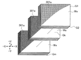
図1に示すウェーハWは、円盤状の半導体ウェーハ(例えば、シリコンウェーハ)であり、その表面Waには、デバイス領域Wa1と、デバイス領域Wa1を囲む外周領域Wa2とが設けられている。デバイス領域Wa1は、格子状に配列された分割予定ラインSで複数の領域に区画されており、各領域にはIC等のデバイスDがそれぞれ形成されている。ウェーハWの外周縁Wdは面取り加工されており断面が略円弧状になっている。
1 Setting of Optimum Conditions (1) Holding Step The wafer W shown in FIG. 1 is a disk-shaped semiconductor wafer (for example, a silicon wafer), and its surface Wa has a device region Wa1 and an outer peripheral region surrounding the device region Wa1. Wa2 and are provided. The device region Wa1 is divided into a plurality of regions by the planned dividing lines S arranged in a grid pattern, and devices D such as ICs are formed in the respective regions. The outer peripheral edge Wd of the wafer W is chamfered to have a substantially arcuate cross section.
図1に示す加工装置1は、ウェーハWに切削加工を施す装置であるとともに、ウェーハWの外周位置を検出することができる装置である。加工装置1に備えられ図1に示すウェーハWを吸引保持する保持テーブル30は、テーブル本体300の外周に環状保持部301が+Z方向に突出するように形成されており、この環状保持部301に囲繞されるように中央に凹み部が形成されている。環状保持部301の上面は、保持テーブル30に載置されたウェーハWの裏面Wbの外周部を吸引保持する環状の保持面301aとなっている。環状保持面301aには、図示しない環状溝又は吸引孔が形成されており、環状溝又は吸引孔には吸引源302が連通している。なお、保持テーブル30は、少なくともZ軸方向を軸として回転可能である。
The processing apparatus 1 shown in FIG. 1 is an apparatus that performs a cutting process on the wafer W and that can detect the outer peripheral position of the wafer W. The holding table 30 which is provided in the processing apparatus 1 and holds the wafer W shown in FIG. 1 by suction is formed on the outer periphery of the
保持ステップでは、ウェーハWを、ウェーハWの中心が保持テーブル30の回転中心に位置するよう位置付けた後、ウェーハWの表面Waが上側になるように保持テーブル30の環状保持面301a上に載置する。そして、環状保持面301aに連通する図示しない吸引源を作動させ、保持テーブル30の環状保持面301a上でウェーハWの裏面Wbの外周部分を吸引してウェーハWを吸引保持する。
In the holding step, after the wafer W is positioned so that the center of the wafer W is located at the rotation center of the holding table 30, the wafer W is placed on the
(2)撮像画像形成ステップ
加工装置1に備える図2に示す撮像手段2は、保持テーブル30で保持されたウェーハWに光を照射する光照射器20と、保持テーブル30で保持されたウェーハWを撮像し撮像画像を形成するカメラ21とを少なくとも有している。光照射器20は、光源200(例えば、LED又はキセノンランプ等)から発する光の光量を、電圧調整器201によって調整できるようになっている。光照射器20には光ファイバー202が接続されており、光源200から発せられた光は、光ファイバー202内を通ってカメラ21の内部に到達する。カメラ21は、外部光が遮光されたケース210と、ケース210内に配設され光照射器20から発せられ光ファイバー202を介して入射した光を下方に向けて反射して方向変換するハーフミラー211と、ハーフミラー211の下側に配設されハーフミラー211で反射した光が入光する対物レンズ212と、ハーフミラー211の上側に配設された撮像素子213とを備えている。ハーフミラー211は、光照射器20から発せられ光ファイバー202を介して入射した光をウェーハWに導く機能と、ウェーハWからの反射光を透過させて撮像素子213に導く機能とを有している。対物レンズ212の光軸は、保持テーブル30に保持されたウェーハWの表面Waに対して直交している。撮像素子213は、ウェーハWからの反射光を受光し、対応する画像を出力する。なお、撮像手段2は、上下動可能であるとともに、水平面方向に移動可能であってもよい。カメラ21には、CPU及びメモリ等の記憶素子等から構成される制御手段9が接続されている。
(2) Imaging Image Forming Step The imaging means 2 shown in FIG. 2 included in the processing apparatus 1 includes a
撮像画像形成ステップでは、図2に示すように、カメラ21の撮像領域内にウェーハWの外周縁Wdがおさまるように、ウェーハWがカメラ21の下方に位置付けられる。その状態で、電圧調整器201によって調整された所定の電圧が光源200に印加されると、光源200は、印加された電圧に対応する光量の光を発する。光源200から発せられた光は、光ファイバー202を通り、ハーフミラー211で反射し、対物レンズ212を介してウェーハWに照射される。そして、ウェーハWからの反射光が、対物レンズ212により集光され、撮像素子213に結像することで、カメラ21によりウェーハWの外周縁Wdを含む撮像画像が形成される。
In the captured image forming step, as shown in FIG. 2, the wafer W is positioned below the
制御手段9は、複数の階層の光量を照射してカメラ21によって撮像したウェーハの外周縁Wdを含む撮像画像を複数形成する撮像画像形成部90を備えており、撮像画像形成部90は、電圧調整器201により光源200に印加する電圧を調整して、光照射器20のウェーハWに対する照射光量を、例えば1%から100%まで1%ずつ変化させて、図3に示すように、カメラ21によりウェーハWの外周縁Wdを含み照射光量が異なる撮像画像G1、撮像画像G2、・・・撮像画像Gk、・・・、撮像画像Gm(mは、本実施形態では100となる。)を形成する。図3においては、形成された撮像画像G1、撮像画像G2、・・・撮像画像Gk・・・、撮像画像Gmを重ねて示している。なお、撮像画像G1、撮像画像G2、・・・撮像画像Gk・・・、撮像画像Gmの形成のための撮像は、カメラ21の高さ位置及びX軸Y軸平面上における位置を固定して行う。形成された計100枚の撮像画像G1、撮像画像G2、・・・撮像画像Gk・・・、撮像画像Gmには、ウェーハWの外周縁の一部及び背景部分(保持テーブル30の環状保持面301aの一部)が表示されている。撮像画像G1、撮像画像G2、・・・撮像画像Gk・・・、撮像画像Gmは、カメラ21から制御手段9の撮像画像形成部90に転送される。
The control unit 9 includes a picked-up image forming section 90 that forms a plurality of picked-up images including the outer peripheral edge Wd of the wafer picked up by the
(3)二値化ステップ
図2に示すように、制御手段9は、複数の階層の光量毎に形成された撮像画像をそれぞれ複数の階層のスライスレベルで二値化して二値化画像を形成する二値化処理部91を備えている。撮像画像形成部90が形成した図3に示す撮像画像G1、撮像画像G2、・・・撮像画像Gk・・・、撮像画像Gmは、二値化処理部91に転送される。
(3) Binarization Step As shown in FIG. 2, the control means 9 binarizes the picked-up images formed for each of the light amounts of the plurality of layers at slice levels of the plurality of layers to form a binarized image. The binarization processing unit 91 is provided. The picked-up image G1, the picked-up image G2, ..., The picked-up image Gk, ..., The picked-up image Gm shown in FIG. 3 formed by the picked-up image forming unit 90 are transferred to the binarization processing unit 91.
二値化処理部91は、複数の階層の光量毎に撮像された撮像画像G1、撮像画像G2、・・・撮像画像Gk・・・、撮像画像Gmを、複数の階層のスライスレベル(閾値)でそれぞれ二値化して複数の二値化画像を形成する。すなわち、二値化処理部91は、例えば、1画素の輝度が0〜255により表示されている複数の撮像画像G1、撮像画像G2、・・・撮像画像Gk・・・、撮像画像Gmを、例えばスライスレベルより輝度値の小さい画素を0とし、スライスレベルより輝度値の大きい画素を255として、二値化画像に変換する。図4に示すように、撮像画像G1に対して、それぞれ二値化スライスレベルの値を0〜255の範囲で1ずつ変化させ、それぞれのスライスレベルを基準として二値化処理を施して、二値化画像G10、G11・・・、G1j、・・・二値化画像G1n(nは255である)を形成する。二値化画像G10、二値化画像G11・・・、二値化画像G1j、・・・二値化画像G1nにおいては、各々設定したスライスレベル未満の輝度値を有する画素を画像中で黒で表示し、設定したスライスレベル以上の輝度値を有する画素を画像中で白で表示している。二値化処理部91は、光量の異なる撮像画像G2〜Gmに対しても同様の処理を行う。このようにして、1枚の撮像画像あたり256枚の二値化画像が形成されることにより、計25600枚の二値化画像が形成される。 The binarization processing unit 91 sets the captured image G1, the captured image G2, ..., The captured image Gk, ..., The captured image Gm captured for each of the light amounts of the plurality of layers to the slice level (threshold) of the plurality of layers. And binarize each to form a plurality of binarized images. That is, the binarization processing unit 91, for example, a plurality of captured images G1, captured images G2, ... For example, a pixel having a luminance value lower than the slice level is set to 0, and a pixel having a luminance value higher than the slice level is set to 255, and the image is converted into a binary image. As shown in FIG. 4, with respect to the captured image G1, the value of the binarized slice level is changed by 1 in the range of 0 to 255, and the binarization processing is performed using each slice level as a reference. The binarized images G1 0 , G1 1, ..., G1 j , ... Binary image G1 n (n is 255) are formed. In the binarized image G1 0 , the binarized image G1 1 ..., The binarized image G1 j , ... The binarized image G1 n , the pixels having the brightness value less than the set slice level are imaged. Pixels having a brightness value equal to or higher than the set slice level are displayed in white in the image. The binarization processing unit 91 performs the same processing on the captured images G2 to Gm having different light amounts. In this way, a total of 25,600 binarized images are formed by forming 256 binarized images for each captured image.
(4)ウェーハ外周位置検出ステップ
図2に示すように、制御手段9は、二値化処理部91で形成された二値化画像における白い画素と黒い画素との境界をウェーハの外周縁の座標位置として検出し記録するウェーハ外周位置検出部92を備えている。ウェーハ外周位置検出部92は、例えば、撮像画像G1に対する二値化画像G10を、図5に示すように、例えば解像度1600×1200の仮想的な出力画面B上に白い画素及び黒い画素に分割して表示し、白い画素と黒い画素との境界のX軸Y軸平面上における座標(x、y)を、ウェーハWの外周縁Wdの座標位置として検出する。そして、図6に示すX軸Y軸座標系上に、検出した各座標を黒点としてプロットし記録していく。図6に示すように、X軸Y軸座標系上には、検出された各座標がウェーハWの円弧に近似する弧状にプロットされていく。
(4) Wafer outer peripheral position detection step As shown in FIG. 2, the control means 9 sets the coordinates of the outer peripheral edge of the wafer at the boundary between the white pixel and the black pixel in the binarized image formed by the binarization processing unit 91. A wafer outer peripheral
同様に、図4に示す撮像画像G1に対する残り255枚の二値化画像G11、G12・・・、G1j、・・・二値化画像G1nからも、それぞれウェーハWの外周縁Wdの座標位置を検出し、図6に示すX軸Y軸座標系上に、取得した各座標をさらにプロットし記録していく。こうして、ウェーハ外周位置検出部92は、撮像画像G1に対する計256枚の二値化画像G10〜二値化画像G1nを基に、ウェーハWの外周縁Wdの座標位置をX軸Y軸座標系上にプロットしたプロット図E1を作成する。
Similarly, from the remaining 255 binarized images G1 1 , G1 2, ..., G1 j , ... Binarized image G1 n with respect to the captured image G1 shown in FIG. The coordinate position is detected, and each acquired coordinate is further plotted and recorded on the X-axis and Y-axis coordinate system shown in FIG. Thus, the wafer outer peripheral
さらに、ウェーハ外周位置検出部92は、残りの撮像画像G2〜Gmに対するそれぞれの256枚の二値化画像についても、撮像画像G1に対してプロット図E1を作成したのと同様に、それぞれのプロット図にプロットしていく。したがって、本実施形態では、ウェーハ外周位置検出部92は、ウェーハWの外周縁Wdの座標位置をX軸Y軸座標系にプロットしたプロット図を、計100図作成する。
Further, the wafer outer peripheral
ウェーハ外周位置検出ステップは、上記のように実施していく以外にも、例えば、以下のように実施してもよい。まず、二値化ステップにおいて取得したすべての二値化画像が、図2に示す二値化処理部91から制御手段9に備えるウェーハ外周位置検出部92に送信される。
The wafer outer peripheral position detection step may be performed as follows, for example, in addition to the above-described steps. First, all the binarized images acquired in the binarization step are transmitted from the binarization processing unit 91 shown in FIG. 2 to the wafer outer peripheral
ウェーハ外周位置検出部92は、例えば図4に示す撮像画像G1に対する二値化画像G10を、図7に示すように、例えば解像度1600×1200の仮想的な出力画面B上に白い画素及び黒い画素に分割して表示する。さらに、仮想的な出力画面B上に、Y座標が一定であるX軸方向に延びる破線で示す直線L3を設定し、二値化画像G10領域内の白い画素と黒い画素との境界と破線L3との交点(x、y)の座標を、ウェーハWの外周縁Wdの座標位置として検出し、図8に示すように、X軸Y軸座標系上に、取得した1つの座標をプロット(図8中の黒点)して記録していく。
Wafer outer
同様に、ウェーハ外周位置検出部92は、撮像画像G1に対する残り255枚の二値化画像G11、G12・・・、G1j、・・・二値化画像G1nからも、各二値化画像領域内の白い画素と黒い画素との境界と破線L3との交点(x、y)の座標を、それぞれウェーハWの外周縁Wdの座標位置として各々1つずつ検出し、図8に示すように、X軸Y軸座標系上に、取得した各座標をさらにプロットし記録していく。すなわち、二値化画像G11〜二値化画像G1nにおける同一Y座標上の各1点をプロットし記憶していく。そして、ウェーハ外周位置検出部92は、撮像画像G1に対する計256枚の二値化画像G10〜二値化画像G1nを基にウェーハWの外周縁Wdの座標位置をX軸Y軸座標系にプロットしたプロット図F1を作成する。図8に示すように、プロット図F1のX軸Y軸座標系上には、同一Y座標上に検出した各座標がX軸方向に向かって直線状に256個プロットされる。なお、仮想的な出力画面B上に、X座標が一定であるY軸方向に延びる直線を設定し、二値化画像G10〜二値化画像G1nにおける各二値化画像領域内の白い画素と黒い画素との境界とY軸方向に平行に延びる直線との交点(x、y)をそれぞれプロットして記憶していくものとしてもよい。
Similarly, the wafer outer peripheral
さらに、ウェーハ外周位置検出部92は、撮像画像G2〜Gmに対する二値化画像についても、プロット図F1を作成したのと同様に、ウェーハWの外周縁Wdの座標位置をX軸Y軸座標系にプロットしたプロット図を作成する。したがって、本実施形態では、ウェーハ外周位置検出部92は、ウェーハWの外周縁Wdの座標位置をX軸Y軸座標系にプロットしたプロット図を、計100図作成する。
Further, the wafer outer peripheral
(5)光量スライスレベル設定ステップ
図2に示すように、制御手段9は、ウェーハ外周位置検出部92で記録された位置座標が最も密集する座標位置の光量とスライスレベルとを最適値として設定する光量スライスレベル設定部93を備えている。まず、図6に示すプロット図E1を含む計100図のプロット図が、ウェーハ外周位置検出部92から光量スライスレベル設定部93に転送される。光量スライスレベル設定部93は、例えば、図6に示すプロット図E1中に黒点で示される位置座標が最も密集する座標を特定し、この領域内にある各座標をプロットした際に用いた二値化画像を、二値化画像G10〜二値化画像G1nの中から特定する。さらに、光量スライスレベル設定部93は、特定した二値化画像から、特定した二値化画像を形成した際のスライスレベルを特定する。例えば、特定した二値化画像がG1j(例えば、jは140)1つである場合には、特定されるスライスレベルもスライスレベルj(例えば、スライスレベル140)となるが、特定した二値化画像が二値化画像G1j−1、二値化画像G1j、二値化画像G1j+1のように3つである場合には、特定されるスライスレベルもスライスレベル(j−1)、スライスレベルj、スライスレベル(j+1)、すなわち、スライスレベル139、スライスレベル140、スライスレベル141となる。
(5) Light amount slice level setting step As shown in FIG. 2, the control means 9 sets the light amount and the slice level at the coordinate position where the position coordinates recorded by the wafer outer peripheral
光量スライスレベル設定部93は、残り99図のプロット図について、同様にスライスレベルを特定していく。例えば、すべてのプロット図から特定されたスライスレベルが、スライスレベルj(例えば、スライスレベル140)1つとなった場合には、スライスレベル140を最適値として決定する。すべてのプロット図から特定されたスライスレベルが、スライスレベル(j−1)、スライスレベルj、スライスレベル(j+1)、すなわち、スライスレベル139、スライスレベル140、スライスレベル141のように3つにまたがる場合には、3つのスライスレベルの中で値が真ん中である値、すなわち中央値であるスライスレベル140を最適値として最終的に決定する。 The light quantity slice level setting unit 93 similarly specifies the slice level for the remaining 99 plot diagrams. For example, when there is only one slice level j (for example, slice level 140) specified from all plots, the slice level 140 is determined as the optimum value. The slice level specified from all the plots extends across three, such as slice level (j−1), slice level j, and slice level (j + 1), that is, slice level 139, slice level 140, and slice level 141. In this case, the value having the middle value among the three slice levels, that is, the slice level 140 that is the median value is finally determined as the optimum value.
光量スライスレベル設定部93は、スライスレベル140を最適値として決定した後、図2に示す光照射器20からのウェーハWに対する照射光量の最適値を決定する。例えば、プロット図E1を含む100枚のプロット図を、スライスレベル140で形成された二値化画像を基にしたプロットのみで構成されるプロット図へとそれぞれ変換する。さらに、変換後の各プロット図を、それぞれのプロット図におけるX軸Y軸を一致させて、同一平面上に重ねて表示して出力し、例えば、バイプロット図を作成する。光量スライスレベル設定部93は、例えば、バイプロット図から位置座標が最も密集する領域を特定し、この領域内にある各座標をプロットした際に用いた二値化画像を、100枚の二値化画像G1140、二値化画像G2140、・・・、二値化画像Gm140の中から特定する。さらに、光量スライスレベル設定部93は、特定した二値化画像から、特定した二値化画像の二値化前の撮像画像を特定する。例えば、特定した撮像画像が1枚のみであり、この1枚が照射光量55%で撮像されたものである場合には、特定される光照射器20のウェーハWに対する最適な照射光量も55%となる。例えば、特定した撮像画像が3枚あり、この三枚がそれぞれ照射光量が54%、55%、56%で撮像されたものである場合には、3つの照射光量の中で値が真ん中である値、すなわち中央値である照射光量55%を最適値として最終的に決定する。なお、図6に示すプロット図E1を含むウェーハWの外周縁Wdの座標位置をX軸Y軸座標系にプロットした計100図のプロット図の代わりに、図8に示すプロット図F1を含む計100図のプロット図を用いて、上記と同様に、スライスレベル及び照射光量の最適値を決定してもよい。この場合は、二値化画像中の外周縁の一部を利用すればよいため、最適条件を求める処理に要する時間を短縮することができる。
After determining the slice level 140 as the optimum value, the light quantity slice level setting unit 93 determines the optimum value of the irradiation light quantity for the wafer W from the
2 ウェーハの外周位置の検出及びウェーハの加工
光量スライスレベル設定ステップを実施した後、光量スライスレベル設定部93が最終的に最適値として決定したスライスレベル140及び照射光量55%という条件を用いて、加工装置1によりウェーハWを円形状にトリミングする切削加工を行う。
2 After performing the detection of the outer peripheral position of the wafer and the wafer processing light quantity slice level setting step, the light quantity slice level setting unit 93 finally uses the slice level 140 and the irradiation light quantity 55% determined as optimum values, A cutting process for trimming the wafer W into a circular shape is performed by the processing device 1.
まず、図2に示すように、カメラ21の撮像領域内にウェーハWの外周縁Wdがおさまるように、ウェーハWがカメラ21の下方に位置付けられる。そして、制御手段9は、光量スライスレベル設定部93に記憶された最適条件を読み込み、電圧調整器201により光源200に印加する電圧を調整して、光照射器20から照射光量55%で光をウェーハWに対して照射し、図9に示すウェーハWの外周縁Wdを含む撮像画像G55を形成する。
First, as shown in FIG. 2, the wafer W is positioned below the
形成された撮像画像G55は、図2に示すカメラ21から制御手段9に転送され、制御手段9の二値化処理部91によってスライスレベル140で二値化されることで、図9に示す二値化画像G55140が形成される。二値化処理部91からウェーハ外周位置検出部92に二値化画像G55140が転送され、ウェーハ外周位置検出部92は、二値化画像G55140を、図10に示すように、例えば解像度1600×1200の仮想的な出力画面B上に白い画素及び黒い画素に分割して表示し、二値化画像G55140領域内の白い画素と黒い画素との境界のX軸Y軸平面上における各座標(x、y)を、ウェーハWの外周縁Wdの座標位置として次々に検出していく。
The formed captured image G55 is transferred from the
このように、上記最適条件の設定の段階において、ウェーハWの外周縁を確実に検出するための光量及びスライスレベルの条件を求め、その条件の下で、実際に加工するウェーハWを撮像して外周縁Wdを検出することにより、実際の外周縁位置と異なる位置をウェーハWの外周縁Wdとして検出してしまうおそれを低減できる。 Thus, in the stage of setting the optimum conditions, the conditions of the light amount and slice level for surely detecting the outer peripheral edge of the wafer W are obtained, and under the conditions, the wafer W to be actually processed is imaged. By detecting the outer peripheral edge Wd, it is possible to reduce the risk of detecting a position different from the actual outer peripheral edge position as the outer peripheral edge Wd of the wafer W.
ウェーハ外周位置検出部92によって、ウェーハWの外周縁Wdの座標位置が検出された後、保持テーブル30に保持されたウェーハWが、図11に示す加工装置1に備える加工手段6の直下に位置付けられる。図11に示すように、保持テーブル30に保持されたウェーハWを加工する加工手段6は、切削手段であり、軸方向がY軸方向であるスピンドル60と、スピンドル60を回転駆動するモータ62と、スピンドル60の先端部に装着された切削ブレード63とを備えており、モータ62がスピンドル60を回転駆動することに伴って、切削ブレード63も高速回転する。さらに、ウェーハ外周位置検出部92が二値化画像G55140から検出したウェーハWの外周縁Wdの座標位置を基準として、加工手段6をY軸方向に移動し、検出したウェーハWの外周縁Wdから所定距離だけ径方向内側の位置に切削ブレード63を位置付ける。例えば、切削ブレード63の端面の約2/3が、ウェーハWの外周縁Wdを含むウェーハWの外周領域Wa2に接触するように切削ブレード63が位置付けられる。
After the wafer outer peripheral
次いで、モータ62がスピンドル60を+Y方向側から見て反時計回り方向に高速回転させることで、スピンドル60に固定されたブレード63を+Y方向側から見て反時計回り方向に高速回転させる。さらに、加工手段6が−Z方向に下降し、切削ブレード63をウェーハWの表面Waから所定深さ切り込ませる。切削ブレード63の切込み深さは、例えば、ウェーハWのトリミング加工後に実施する研削加工におけるウェーハWの研削量に基づいて決定される。切削ブレード63を所定の高さ位置まで切込み送りした後、切削ブレード63を+Y方向側から見て時計回り方向に高速回転させ続けた状態で、保持テーブル30を+Z方向側から見て反時計方向に360度回転させることで、ウェーハWの外周縁Wd全周を切削しトリミングする。他のウェーハWについても、設定された同じ条件の下で外周縁Wdを検出し、トリミングしていく。
Then, the
このように、最適条件の設定の段階において、ウェーハWの外周縁Wdを確実に検出するための光量及びスライスレベルの条件を求め、その条件の下で、実際に加工するウェーハWを撮像して外周縁Wdを検出し、その位置を基準としてブレード63を切り込ませるため、所望の位置を切削することができる。
Thus, at the stage of setting the optimum conditions, the conditions of the light amount and the slice level for surely detecting the outer peripheral edge Wd of the wafer W are obtained, and under that condition, the wafer W to be actually processed is imaged. Since the outer peripheral edge Wd is detected and the
なお、本発明に係るウェーハの外周位置を検出するウェーハの検出方法は、上記実施形態に限定されるものではない。例えば、ウェーハWに照射する光の光量及び二値化時のスライスレベルの階層は、本実施形態の例には限定されない。 The wafer detection method for detecting the outer peripheral position of the wafer according to the present invention is not limited to the above embodiment. For example, the light amount of the light with which the wafer W is irradiated and the slice level hierarchy at the time of binarization are not limited to the example of the present embodiment.
1:加工装置
30:保持テーブル 300:テーブル本体 301:環状保持部
301a:環状保持面 302:吸引源
2:撮像手段 20:光照射器 200:光源 201:電圧調整器
202:光ファイバー 21:カメラ 210:ケース 211:ハーフミラー
212:対物レンズ 213:撮像素子
6:加工手段 60:スピンドル 62:モータ 63:切削ブレード
9:制御手段 90:撮像画像形成部 91:二値化処理部
92:ウェーハ外周位置検出部 93:光量スライスレベル設定部
W:ウェーハ Wa:ウェーハの表面 Wb:ウェーハの裏面 Wa1:デバイス領域
Wa2:外周領域 S:分割予定ライン D:デバイス Wd:外周縁
1: processing device 30: holding table 300: table body 301: annular holding
Claims (4)
該保持テーブルでウェーハを保持する保持ステップと、
該保持ステップを実施した後、該保持テーブルで保持されたウェーハに該光照射器から複数の階層の光量を照射し該カメラで撮像してウェーハの外周縁を含む撮像画像を複数形成する撮像画像形成ステップと、
該撮像画像形成ステップを実施した後、複数の階層の光量毎に撮像された該撮像画像をそれぞれ複数の階層のスライスレベルで二値化して二値化画像を形成する二値化ステップと、
該二値化ステップで形成された該二値化画像における白い画素と黒い画素との境界をウェーハの外周縁の座標位置として検出し記録するウェーハ外周位置検出ステップと、
該ウェーハ外周位置検出ステップで記録された位置座標が最も密集する座標位置の光量とスライスレベルとを最適値として設定する光量スライスレベル設定ステップと、を備えたウェーハの検出方法。 A holding table having a holding surface for holding the wafer; a light irradiator for irradiating the wafer held by the holding table with light; and a camera for imaging the wafer held by the holding table and forming a picked-up image. A method of detecting a wafer, which detects an outer peripheral position of a wafer by using an apparatus including the image pickup means,
A holding step of holding the wafer on the holding table;
After performing the holding step, the wafer held by the holding table is irradiated with light amounts of a plurality of layers from the light irradiator and is imaged by the camera to form a plurality of imaged images including the outer peripheral edge of the wafer. A forming step,
After performing the captured image forming step, a binarization step of forming a binarized image by binarizing the captured images captured for each of the light amounts of a plurality of layers at slice levels of a plurality of layers, respectively.
A wafer outer peripheral position detecting step of detecting and recording a boundary between a white pixel and a black pixel in the binarized image formed in the binarizing step as a coordinate position of an outer peripheral edge of the wafer,
A wafer detection method comprising: a light quantity slice level setting step of setting a light quantity at a coordinate position where the position coordinates recorded in the wafer outer peripheral position detection step are most dense and a slice level as optimum values.
該制御手段は、
該保持テーブルで保持されたウェーハに該光照射器から複数の階層の光量を照射し該カメラで撮像して形成したウェーハの外周縁を含む撮像画像を複数形成する撮像画像形成部と、
複数の階層の光量毎に形成された該撮像画像をそれぞれ複数の階層のスライスレベルで二値化して二値化画像を形成する二値化処理部と、
該二値化処理部で形成された該二値化画像における白い画素と黒い画素との境界をウェーハの外周縁の座標位置として検出し記録するウェーハ外周位置検出部と、
該ウェーハ外周位置検出部で記録された位置座標が最も密集する座標位置の光量とスライスレベルとを最適値として設定する光量スライスレベル設定部と、を備えた加工装置。 A holding table having a holding surface for holding the wafer; a light irradiator for irradiating the wafer held by the holding table with light; and a camera for imaging the wafer held by the holding table and forming a picked-up image. And a processing unit that processes the wafer held by the holding table, and a control unit that controls at least the processing unit.
The control means is
A picked-up image forming unit that forms a plurality of picked-up images including the outer peripheral edge of the wafer formed by irradiating the wafers held by the holding table with light quantities of a plurality of layers from the light irradiator and picked up by the camera,
A binarization processing unit that binarizes the captured images formed for each of the light amounts of a plurality of layers at slice levels of a plurality of layers to form a binarized image,
A wafer outer peripheral position detection unit that detects and records a boundary between a white pixel and a black pixel in the binarized image formed by the binarization processing unit as a coordinate position of an outer peripheral edge of the wafer,
A processing apparatus comprising: a light amount slice level setting unit that sets a light amount at a coordinate position where the position coordinates recorded by the wafer outer peripheral position detection unit are most dense and a slice level as optimum values.
Priority Applications (1)
| Application Number | Priority Date | Filing Date | Title |
|---|---|---|---|
| JP2016112564A JP6697328B2 (en) | 2016-06-06 | 2016-06-06 | Wafer detecting method for detecting outer peripheral position of wafer and processing apparatus capable of detecting outer peripheral position of wafer |
Applications Claiming Priority (1)
| Application Number | Priority Date | Filing Date | Title |
|---|---|---|---|
| JP2016112564A JP6697328B2 (en) | 2016-06-06 | 2016-06-06 | Wafer detecting method for detecting outer peripheral position of wafer and processing apparatus capable of detecting outer peripheral position of wafer |
Publications (2)
| Publication Number | Publication Date |
|---|---|
| JP2017219364A JP2017219364A (en) | 2017-12-14 |
| JP6697328B2 true JP6697328B2 (en) | 2020-05-20 |
Family
ID=60657006
Family Applications (1)
| Application Number | Title | Priority Date | Filing Date |
|---|---|---|---|
| JP2016112564A Active JP6697328B2 (en) | 2016-06-06 | 2016-06-06 | Wafer detecting method for detecting outer peripheral position of wafer and processing apparatus capable of detecting outer peripheral position of wafer |
Country Status (1)
| Country | Link |
|---|---|
| JP (1) | JP6697328B2 (en) |
Families Citing this family (3)
| Publication number | Priority date | Publication date | Assignee | Title |
|---|---|---|---|---|
| JP7393926B2 (en) * | 2019-11-27 | 2023-12-07 | 株式会社ディスコ | processing equipment |
| JP7418919B2 (en) * | 2020-03-18 | 2024-01-22 | 株式会社ディスコ | Selection method for selecting detection conditions for wafer outer edge position |
| JP7423157B2 (en) | 2020-04-30 | 2024-01-29 | 株式会社ディスコ | How to manage processing equipment |
Family Cites Families (7)
| Publication number | Priority date | Publication date | Assignee | Title |
|---|---|---|---|---|
| JPH07113962B2 (en) * | 1986-12-19 | 1995-12-06 | マツダ株式会社 | Image processing method |
| JP2008076277A (en) * | 2006-09-22 | 2008-04-03 | I-Pulse Co Ltd | Inspection system and inspection method |
| JP4823996B2 (en) * | 2007-11-02 | 2011-11-24 | 日本電産トーソク株式会社 | Outline detection method and outline detection apparatus |
| KR101442153B1 (en) * | 2008-01-15 | 2014-09-25 | 삼성전자 주식회사 | Low-light image processing method and system |
| JP5829881B2 (en) * | 2011-10-07 | 2015-12-09 | 株式会社ディスコ | Cutting equipment |
| JP6242619B2 (en) * | 2013-07-23 | 2017-12-06 | 株式会社ディスコ | Processing equipment |
| JP6174980B2 (en) * | 2013-11-22 | 2017-08-02 | 株式会社ディスコ | Wafer detection method |
-
2016
- 2016-06-06 JP JP2016112564A patent/JP6697328B2/en active Active
Also Published As
| Publication number | Publication date |
|---|---|
| JP2017219364A (en) | 2017-12-14 |
Similar Documents
| Publication | Publication Date | Title |
|---|---|---|
| TW201738950A (en) | Wafer processing method | |
| JP6697328B2 (en) | Wafer detecting method for detecting outer peripheral position of wafer and processing apparatus capable of detecting outer peripheral position of wafer | |
| JP7427333B2 (en) | Edge alignment method | |
| KR20200071670A (en) | Cutting apparatus and wafer processing method using cutting apparatus | |
| KR20100067659A (en) | Monitoring apparatus, monitoring method, inspecting apparatus and inspecting method | |
| CN111801545B (en) | Line shape inspection device and line shape inspection method | |
| TWI824071B (en) | Central detection method | |
| KR102257264B1 (en) | Scratch detecting method | |
| JP6065343B2 (en) | Edge detection device | |
| KR20210025478A (en) | Quality determination method of machining result of laser machining apparatus | |
| JP2019155481A (en) | Cutting device | |
| JP6671253B2 (en) | Wafer detection method for detecting outer peripheral position of wafer and processing apparatus capable of detecting outer peripheral position of wafer | |
| JP6283971B2 (en) | Edge detection device | |
| JP6229789B2 (en) | Edge detection device | |
| JP7418919B2 (en) | Selection method for selecting detection conditions for wafer outer edge position | |
| JP2024160046A (en) | Workpiece inspection method and device | |
| JP6132682B2 (en) | Key pattern detection method | |
| JP2013063490A (en) | Cutting apparatus and cutting method | |
| JP2013191775A (en) | Component mounting device and component shape measuring method | |
| JP6065342B2 (en) | Edge detection device | |
| JP2021104542A (en) | Laser processing device and method | |
| US11680911B2 (en) | Marking inspection device, marking inspection method and article inspection apparatus | |
| JP2014239134A (en) | Wafer processing method | |
| JP7562858B2 (en) | Recognition device and recognition method | |
| US20240307998A1 (en) | Microscope |
Legal Events
| Date | Code | Title | Description |
|---|---|---|---|
| A621 | Written request for application examination |
Free format text: JAPANESE INTERMEDIATE CODE: A621 Effective date: 20190424 |
|
| A977 | Report on retrieval |
Free format text: JAPANESE INTERMEDIATE CODE: A971007 Effective date: 20200318 |
|
| TRDD | Decision of grant or rejection written | ||
| A01 | Written decision to grant a patent or to grant a registration (utility model) |
Free format text: JAPANESE INTERMEDIATE CODE: A01 Effective date: 20200331 |
|
| A61 | First payment of annual fees (during grant procedure) |
Free format text: JAPANESE INTERMEDIATE CODE: A61 Effective date: 20200424 |
|
| R150 | Certificate of patent or registration of utility model |
Ref document number: 6697328 Country of ref document: JP Free format text: JAPANESE INTERMEDIATE CODE: R150 |
|
| R250 | Receipt of annual fees |
Free format text: JAPANESE INTERMEDIATE CODE: R250 |
|
| R250 | Receipt of annual fees |
Free format text: JAPANESE INTERMEDIATE CODE: R250 |