以下では、本発明の実施形態および参考例(第1〜第8参考例)に係る形態を、添付図面を参照して詳細に説明する。
<第1実施形態>
図1は、本発明の第1実施形態に係るチップ部品1の模式的な斜視図である。なお、図1では、説明の便宜上、後述する第1および第2接続電極3,4をクロスハッチングで示している。
Below, the form which concerns on embodiment and reference example (1st-8th reference example) of this invention is demonstrated in detail with reference to an accompanying drawing.
First Embodiment
FIG. 1 is a schematic perspective view of a chip part 1 according to a first embodiment of the present invention. In FIG. 1, for convenience of explanation, first and second connection electrodes 3 and 4 described later are shown by cross hatching.
チップ部品1は、微小なチップ部品であり、図1に示すように、略直方体形状をなしている。チップ部品1の平面形状は、たとえば長辺81に沿う長さL1が0.6mm以下、短辺82に沿う長さW1が0.3mm以下の矩形(0603チップ)であってもよいし、長辺81に沿う長さL1が0.4mm以下、短辺82に沿う長さW1が0.2mm以下の矩形(0402チップ)であってもよい。より好ましくは、チップ部品1の寸法に関し、長辺81に沿う長さL1が0.3mm、短辺82に沿う長さW1が0.15mmの矩形(03015チップ)である。チップ部品1の厚さT1は、たとえば0.1mmである。
The chip part 1 is a minute chip part, and as shown in FIG. 1, has a substantially rectangular parallelepiped shape. The planar shape of the chip component 1 may be, for example, a rectangle (0603 chip) in which the length L1 along the long side 81 is 0.6 mm or less and the length W1 along the short side 82 is 0.3 mm or less It may be a rectangle (0402 chip) in which the length L1 along the side 81 is 0.4 mm or less and the length W1 along the short side 82 is 0.2 mm or less. More preferably, regarding the dimensions of the chip part 1, the length L1 along the long side 81 is 0.3 mm, and the length W1 along the short side 82 is a rectangle (03015 chip) having a length of 0.15 mm. The thickness T1 of the chip part 1 is, for example, 0.1 mm.
チップ部品1は、チップ部品1の本体を構成する基板2と、第1および第2接続電極3,4と、第1および第2接続電極3,4によって外部接続される回路素子が選択的に形成される素子領域5とを主に備えている。
基板2は、略直方体のチップ形状である。基板2において図1における上面をなす一つの表面は、素子形成面2Aである。素子形成面2Aは、基板2において回路素子が形成される表面であり、略長方形状である。基板2の厚さ方向において素子形成面2Aとは反対側の面は、裏面2Bである。素子形成面2Aと裏面2Bとは、略同寸法かつ同形状であり、互いに平行である。素子形成面2Aにおける一対の長辺81および短辺82によって区画された矩形状の縁を、周縁部85ということにし、裏面2Bにおける一対の長辺81および短辺82によって区画された矩形状の縁を、周縁部90ということにする。素子形成面2A(裏面2B)に直交する法線方向から見ると、周縁部85と周縁部90とは、重なっている。
In the chip part 1, a circuit element connected externally by the substrate 2 constituting the main body of the chip part 1, the first and second connection electrodes 3 and 4, and the first and second connection electrodes 3 and 4 is selectively selected. An element region 5 to be formed is mainly provided.
The substrate 2 has a substantially rectangular chip shape. One surface forming the upper surface in FIG. 1 in the substrate 2 is an element forming surface 2A. The element forming surface 2A is a surface of the substrate 2 on which a circuit element is formed, and has a substantially rectangular shape. The surface opposite to the element forming surface 2A in the thickness direction of the substrate 2 is the back surface 2B. The element forming surface 2A and the back surface 2B have substantially the same size and shape, and are parallel to each other. A rectangular edge partitioned by a pair of long sides 81 and short sides 82 in the element forming surface 2A is referred to as a peripheral portion 85, and a rectangular shape partitioned by a pair of long sides 81 and short sides 82 in the back surface 2B. The edge will be referred to as the rim 90. When viewed from the normal direction orthogonal to the element formation surface 2A (rear surface 2B), the peripheral edge portion 85 and the peripheral edge portion 90 overlap.
基板2は、素子形成面2Aおよび裏面2B以外の表面として、複数の側面(側面2C、側面2D、側面2Eおよび側面2F)を有している。当該複数の側面2C〜2Fは、素子形成面2Aおよび裏面2Bのそれぞれに交差(詳しくは、直交)して延びて、素子形成面2Aおよび裏面2Bの間を繋いでいる。
側面2Cは、素子形成面2Aおよび裏面2Bにおける長手方向一方側(図1における左手前側)の短辺82間に架設されていて、側面2Dは、素子形成面2Aおよび裏面2Bにおける長手方向他方側(図1における右奥側)の短辺82間に架設されている。側面2Cおよび側面2Dは、当該長手方向における基板2の両端面である。側面2Eは、素子形成面2Aおよび裏面2Bにおける短手方向一方側(図1における左奥側)の長辺81間に架設されていて、側面2Fは、素子形成面2Aおよび裏面2Bにおける短手方向他方側(図1における右手前側)の長辺81間に架設されている。側面2Eおよび側面2Fは、当該短手方向における基板2の両端面である。側面2Cおよび側面2Dのそれぞれは、側面2Eおよび側面2Fのそれぞれと交差(詳しくは、直交)している。そのため、素子形成面2A〜側面2Fにおいて隣り合うもの同士が直角をなしている。
The substrate 2 has a plurality of side surfaces (side surface 2C, side surface 2D, side surface 2E and side surface 2F) as the surface other than the element forming surface 2A and the back surface 2B. The plurality of side surfaces 2C to 2F extend across (in detail, at right angles) the element forming surface 2A and the back surface 2B to connect the element forming surface 2A and the back surface 2B.
Side surface 2C is provided between short sides 82 of element forming surface 2A and back surface 2B in the longitudinal direction one side (left front side in FIG. 1), and side surface 2D is the other side in the longitudinal direction on element forming surface 2A and back surface 2B. It is installed between the short sides 82 (right back side in FIG. 1). The side surface 2C and the side surface 2D are both end surfaces of the substrate 2 in the longitudinal direction. Side surface 2E is bridged between long sides 81 of element forming surface 2A and back surface 2B in the short side (left back side in FIG. 1), and side surface 2F is short on element forming surface 2A and back surface 2B. It is bridged between the long sides 81 of the other direction side (the right front side in FIG. 1). The side surface 2E and the side surface 2F are both end surfaces of the substrate 2 in the short direction. Each of the side surface 2C and the side surface 2D intersects (specifically, is orthogonal to) each of the side surface 2E and the side surface 2F. Therefore, adjacent ones of the element formation surface 2A to the side surface 2F form a right angle.
素子形成面2Aは、その長手方向において、第1接続電極3が形成される一端部と、第2接続電極4が形成される他端部とを含む。素子形成面2Aの一端部は、基板2の側面2D側の端部であり、素子形成面2Aの他端部は、基板2の側面2C側の端部である。素子形成面2Aの他端部には、貫通孔6が形成されている。貫通孔6は、素子形成面2Aから厚さ方向に向かって裏面2Bを貫通している。
The element forming surface 2A includes, in the longitudinal direction, one end where the first connection electrode 3 is formed and the other end where the second connection electrode 4 is formed. One end of the element forming surface 2A is an end on the side 2D side of the substrate 2, and the other end of the element forming surface 2A is an end on the side 2C of the substrate 2. A through hole 6 is formed at the other end of the element forming surface 2A. The through hole 6 penetrates the back surface 2B in the thickness direction from the element forming surface 2A.
貫通孔6は、平面視略矩形状に形成されており、隣接する面同士が互いに直角に交わる4つの壁面66を有している。4つの壁面66は、素子形成面2Aと裏面2Bとの間に架設されており、基板2の素子形成面2Aおよび裏面2Bと直角をなすように形成されている。貫通孔6の基板2の長辺81に沿う方向の長さは、0.025μm〜0.05mmであり、貫通孔6の短辺82に沿う方向の長さは、0.5μm〜0.1mmであることが好ましい。
The through hole 6 is formed in a substantially rectangular shape in a plan view, and has four wall surfaces 66 in which adjacent surfaces intersect with each other at a right angle. The four wall surfaces 66 are provided between the element forming surface 2A and the back surface 2B, and are formed to be perpendicular to the element forming surface 2A and the back surface 2B of the substrate 2. The length of the through hole 6 in the direction along the long side 81 of the substrate 2 is 0.025 μm to 0.05 mm, and the length in the direction along the short side 82 of the through hole 6 is 0.5 μm to 0.1 mm Is preferred.
なお、本実施形態では、平面視略矩形状の貫通孔6が形成されている例について説明するが、貫通孔6は、平面視円形状、平面視多角形状等の任意の形状であってもよい。
基板2では、素子形成面2A、側面2C〜2F、および貫通孔6の壁面66のそれぞれの全域がパッシベーション膜23で覆われている。そのため、厳密には、図1では、素子形成面2A、側面2C〜2F、および貫通孔6の壁面66のそれぞれの全域は、パッシベーション膜23の内側(裏側)に位置していて、外部に露出されていない。さらに、チップ部品1は、樹脂膜24を有している。樹脂膜24は、素子形成面2A上のパッシベーション膜23の全域(周縁部85およびその内側領域)を覆っている。パッシベーション膜23および樹脂膜24については、以降で詳説する。
In this embodiment, an example in which the through hole 6 having a substantially rectangular shape in plan view is formed will be described, but the through hole 6 may have any shape such as a circular shape in plan view or a polygonal shape in plan view. Good.
In the substrate 2, the entire region of the element formation surface 2 A, the side surfaces 2 C to 2 F, and the wall surface 66 of the through hole 6 is covered with the passivation film 23. Therefore, strictly speaking, in FIG. 1, the entire regions of element formation surface 2A, side surfaces 2C to 2F, and wall surface 66 of through hole 6 are located on the inner side (back side) of passivation film 23 and exposed to the outside. It has not been. Furthermore, the chip part 1 has a resin film 24. The resin film 24 covers the entire region (the peripheral portion 85 and the inner region thereof) of the passivation film 23 on the element formation surface 2A. The passivation film 23 and the resin film 24 will be described in detail later.
第1および第2接続電極3,4は、素子形成面2Aの一端部と、他端部とに配置されており、互いに間隔を開けて形成されている。
第1接続電極3は、平面視における4辺をなす一対の長辺3Aおよび一対の短辺3B、ならびに周縁部86を有している。第1接続電極3の長辺3Aと短辺3Bとは平面視において直交している。第1接続電極3の周縁部86は、基板2の素子形成面2A上において周縁部85を覆うように、素子形成面2Aおよび側面2C,2E,2Fに跨るように一体的に形成されている。本実施形態では、周縁部86は、基板2の側面2C,2E,2F同士が交わる各コーナー部11を覆うように形成されている。
The first and second connection electrodes 3 and 4 are disposed at one end and the other end of the element forming surface 2A, and are formed spaced apart from each other.
The first connection electrode 3 has a pair of long sides 3A and a pair of short sides 3B, which form four sides in a plan view, and a peripheral edge portion 86. The long side 3A and the short side 3B of the first connection electrode 3 are orthogonal to each other in plan view. The peripheral portion 86 of the first connection electrode 3 is integrally formed so as to cover the element forming surface 2A and the side surfaces 2C, 2E, and 2F so as to cover the peripheral portion 85 on the element forming surface 2A of the substrate 2 . In the present embodiment, the peripheral edge portion 86 is formed so as to cover each corner portion 11 where the side surfaces 2C, 2E, 2F of the substrate 2 intersect.
一方、第2接続電極4は、平面視における4辺をなす一対の長辺4Aおよび一対の短辺4Bと、周縁部87と、開口部63とを含む。第2接続電極4の長辺4Aと短辺4Bとは平面視において直交している。第2接続電極4の周縁部87は、基板2の素子形成面2A上において周縁部85を覆うように、素子形成面2Aおよび側面2D,2E,2Fに跨るように一体的に形成されている。本実施形態では、周縁部87は、基板2の側面2D,2E,2F同士が交わる各コーナー部11を覆うように形成されている。
On the other hand, the second connection electrode 4 includes a pair of long sides 4A and a pair of short sides 4B forming four sides in a plan view, a peripheral edge portion 87, and an opening 63. The long side 4A and the short side 4B of the second connection electrode 4 are orthogonal to each other in plan view. The peripheral portion 87 of the second connection electrode 4 is integrally formed so as to cover the element forming surface 2A and the side surfaces 2D, 2E, and 2F so as to cover the peripheral portion 85 on the element forming surface 2A of the substrate 2 . In the present embodiment, the peripheral edge portion 87 is formed so as to cover each corner portion 11 where the side surfaces 2D, 2E, 2F of the substrate 2 intersect.
本実施形態では、第2接続電極4の中央部に開口部63が形成されている。すなわち、前述の貫通孔6は、第2接続電極4の中央部に開口部63が形成される部分に形成されている。第2接続電極4の開口部63は、基板2に形成された貫通孔6の壁面66を覆うように、素子形成面2Aおよび当該壁面66に跨るように一体的に形成されている。これにより、第2接続電極4における貫通孔6が形成された領域は、貫通孔6と同程度の大きさの開口部63によって開放されており、貫通孔6(貫通孔6の壁面66)が当該開口部63から外部に露出している。このように、第2接続電極4は、平面視において第1接続電極3よりも小さい面積で相異なる形状に形成されている。
In the present embodiment, an opening 63 is formed at the center of the second connection electrode 4. That is, the above-mentioned through hole 6 is formed in a portion in which the opening 63 is formed in the central portion of the second connection electrode 4. The opening 63 of the second connection electrode 4 is integrally formed so as to straddle the element forming surface 2 A and the wall surface 66 so as to cover the wall surface 66 of the through hole 6 formed in the substrate 2. Thus, the region of the second connection electrode 4 in which the through hole 6 is formed is opened by the opening 63 having the same size as the through hole 6, and the through hole 6 (the wall surface 66 of the through hole 6) It is exposed to the outside from the opening 63. Thus, the second connection electrodes 4 are formed in different shapes in a smaller area than the first connection electrodes 3 in a plan view.
なお、基板2は、各コーナー部11が平面視で面取りされたラウンド形状となっていてもよい。この場合、チップ部品1の製造工程や実装時におけるチッピングを抑制できる構造となる。
素子領域5には、回路素子が形成されている。回路素子は、基板2の素子形成面2Aにおける第1接続電極3と第2接続電極4との間の領域に形成されていて、パッシベーション膜23および樹脂膜24によって上から被覆されている。
The substrate 2 may have a round shape in which each corner portion 11 is chamfered in plan view. In this case, it is possible to suppress chipping during the manufacturing process or mounting of the chip part 1.
Circuit elements are formed in the element region 5. The circuit element is formed in a region between the first connection electrode 3 and the second connection electrode 4 on the element forming surface 2A of the substrate 2, and is covered from above with the passivation film 23 and the resin film 24.
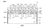
図2は、図1に示すチップ部品1の平面図である。図3は、図2に示す切断面線III−IIIから見た断面図である。図4は、図2に示す切断面線IV−IVから見た断面図である。
チップ部品1は、基板2と、基板2に形成された複数のダイオードセルD101〜D104と、これらの複数のダイオードセルD101〜D104を並列に接続するカソード電極膜103およびアノード電極膜104とを含む。カソード電極膜103には、第1接続電極3が接続され、アノード電極膜104には、第2接続電極4が接続されている。つまり、本実施形態では、第1接続電極3はカソード電極であり、第2接続電極4はアノード電極である。したがって、図1において説明した貫通孔6(開口部63)は、本実施形態では、第2接続電極4の極性方向を示すアノードマークAM1として機能する。
FIG. 2 is a plan view of the chip part 1 shown in FIG. FIG. 3 is a cross-sectional view as viewed from the section line III-III shown in FIG. FIG. 4 is a cross-sectional view as seen from the section line IV-IV shown in FIG.
The chip part 1 includes a substrate 2, a plurality of diode cells D101 to D104 formed on the substrate 2, and a cathode electrode film 103 and an anode electrode film 104 connecting the plurality of diode cells D101 to D104 in parallel. . The first connection electrode 3 is connected to the cathode electrode film 103, and the second connection electrode 4 is connected to the anode electrode film 104. That is, in the present embodiment, the first connection electrode 3 is a cathode electrode, and the second connection electrode 4 is an anode electrode. Therefore, the through hole 6 (the opening 63) described in FIG. 1 functions as an anode mark AM1 indicating the polarity direction of the second connection electrode 4 in the present embodiment.
基板2は、本実施形態では、p+型の半導体基板(たとえばシリコン基板)である。基板2の両端部に、第1接続電極3との接続のためのカソードパッド105と、第2接続電極4との接続のためのアノードパッド106とが配置されている。これらのパッド105,106の間(すなわち、素子領域5)に、ダイオードセル領域107が設けられている。
The substrate 2 is a p + -type semiconductor substrate (for example, a silicon substrate) in the present embodiment. A cathode pad 105 for connection to the first connection electrode 3 and an anode pad 106 for connection to the second connection electrode 4 are disposed at both ends of the substrate 2. A diode cell region 107 is provided between the pads 105 and 106 (ie, the device region 5).
ダイオードセル領域107は、本実施形態では、矩形に形成されている。ダイオードセル領域107内に、複数のダイオードセルD101〜D104が配置されている。複数のダイオードセルD101〜D104は、本実施形態では4個設けられており、基板2の長手方向および短手方向に沿って、マトリックス状に等間隔で二次元配列されている。
図5は、図1に示すチップ部品において、カソード電極膜103およびアノード電極膜104ならびにその上に形成された構成を取り除いて、基板2の表面の構造を示す平面図である。ダイオードセルD101〜D104の各領域内には、それぞれ、p+型の基板2の表層領域にn+型領域110が形成されている。n+型領域110は、個々のダイオードセル毎に分離されている。これにより、ダイオードセルD101〜D104は、ダイオードセル毎に分離されたpn接合領域111をそれぞれ有している。
The diode cell region 107 is formed in a rectangular shape in the present embodiment. In the diode cell region 107, a plurality of diode cells D101 to D104 are arranged. In the present embodiment, four diode cells D101 to D104 are provided, and are arranged two-dimensionally at equal intervals in a matrix along the longitudinal direction and the short direction of the substrate 2.
FIG. 5 is a plan view showing the structure of the surface of the substrate 2 by removing the cathode electrode film 103 and the anode electrode film 104 and the configuration formed thereon in the chip part shown in FIG. In each region of the diode cells D101 to D104, an n + -type region 110 is formed in the surface layer region of the p + -type substrate 2, respectively. The n + -type region 110 is separated into individual diode cells. Thus, the diode cells D101 to D104 respectively have pn junction regions 111 separated for each diode cell.
複数のダイオードセルD101〜D104は、本実施形態では等しい大きさおよび等しい形状、具体的には矩形形状に形成されており、各ダイオードセルの矩形領域内に、多角形形状のn+型領域110が形成されている。本実施形態では、n+型領域110は、正八角形に形成されており、ダイオードセルD101〜D104の矩形領域を形成する4辺にそれぞれ沿う4つの辺と、ダイオードセルD101〜D104の矩形領域の4つの角部にそれぞれ対向する別の4つの辺とを有している。基板2の表層領域には、さらに、n+型領域110から所定の間隔を空けて分離された状態でp+型領域112が形成されている。p+型領域112は、ダイオードセル領域107内において、カソード電極膜103が配置される領域を回避したパターンに形成されている。
The plurality of diode cells D101 to D104 are formed to have the same size and the same shape in the present embodiment, specifically, a rectangular shape, and the polygon shaped n + -type region 110 is formed in the rectangular region of each diode cell. Is formed. In the present embodiment, the n + -type region 110 is formed in a regular octagon, and includes four sides along the four sides forming the rectangular regions of the diode cells D101 to D104 and the rectangular regions of the diode cells D101 to D104. It has another four sides opposite to the four corners respectively. In the surface layer region of the substrate 2, ap + -type region 112 is further formed in a state of being separated from the n + -type region 110 at a predetermined interval. The p + -type region 112 is formed in a pattern avoiding the region where the cathode electrode film 103 is disposed in the diode cell region 107.
図3および図4に示されているように、基板2の表面には、酸化膜等からなる絶縁膜115(図1および図2では図示省略)が形成されている。絶縁膜115には、ダイオードセルD101〜D104のそれぞれのn+型領域110の表面を露出させるコンタクト孔116と、p+型領域112を露出させるコンタクト孔117とが形成されている。絶縁膜115の表面には、カソード電極膜103およびアノード電極膜104が形成されている。
As shown in FIGS. 3 and 4, an insulating film 115 (not shown in FIGS. 1 and 2) formed of an oxide film or the like is formed on the surface of the substrate 2. In the insulating film 115, a contact hole 116 for exposing the surface of the n + -type region 110 of each of the diode cells D101 to D104 and a contact hole 117 for exposing the p + -type region 112 are formed. A cathode electrode film 103 and an anode electrode film 104 are formed on the surface of the insulating film 115.
カソード電極膜103は、絶縁膜115の表面からコンタクト孔116内に入り込み、このコンタクト孔116内でダイオードセルD101〜D104の各n+型領域110との間でオーミック接触を形成している。アノード電極膜104は、絶縁膜115の表面からコンタクト孔117の内方へと延びており、コンタクト孔117内でp+型領域112との間でオーミック接触を形成している。カソード電極膜103およびアノード電極膜104は、本実施形態では、同じ材料からなる電極膜からなっている。
The cathode electrode film 103 enters the contact hole 116 from the surface of the insulating film 115, and forms an ohmic contact with the n + -type regions 110 of the diode cells D101 to D104 in the contact hole 116. The anode electrode film 104 extends from the surface of the insulating film 115 to the inside of the contact hole 117, and forms an ohmic contact with the p + -type region 112 in the contact hole 117. The cathode electrode film 103 and the anode electrode film 104 are made of an electrode film made of the same material in the present embodiment.
カソード電極膜103およびアノード電極膜104としては、Ti膜を下層としAl膜を上層としたTi/Al積層膜や、AlCu膜を適用できる。その他、AlSi膜を電極膜として用いることもできる。AlSi膜を用いると、基板2の表面にp+型領域112を設けることなく、アノード電極膜104と基板2との間でオーミック接触を形成することができる。したがって、p+型領域112を形成するための工程を省くことができる。
As the cathode electrode film 103 and the anode electrode film 104, a Ti / Al laminated film in which a Ti film is a lower layer and an Al film is an upper layer, or an AlCu film can be applied. Besides, an AlSi film can also be used as an electrode film. When an AlSi film is used, an ohmic contact can be formed between the anode electrode film 104 and the substrate 2 without providing the p + -type region 112 on the surface of the substrate 2. Therefore, the process for forming p + -type region 112 can be omitted.
カソード電極膜103およびアノード電極膜104の間は、スリット118によって分離されている。本実施形態では、スリット118は、ダイオードセルD101〜D104のn+型領域110を縁取るように、n+型領域110の平面形状と整合する枠形状(すなわち正八角形枠状)に形成されている。それに応じて、カソード電極膜103は、n+型領域110の形状に整合する平面形状(すなわち正八角形形状)のセル接合部103aを各ダイオードセルD101〜D104の領域に有し、当該セル接合部103aの間が直線状の架橋部103bによって連絡されており、さらに、直線状の別の架橋部103cによってカソードパッド105の直下に形成された大きな矩形形状の外部接続部103dへと接続されている。一方、アノード電極膜104は、略一定の幅のスリット118に対応した間隔を開けて、カソード電極膜103を取り囲むように、絶縁膜115の表面に形成されていて、アノードパッド106の直下の矩形領域へ延びて一体的に形成されている。
The cathode electrode film 103 and the anode electrode film 104 are separated by a slit 118. In this embodiment, the slits 118 are formed in a frame shape (that is, a regular octagonal frame shape) that matches the planar shape of the n + -type region 110 so as to border the n + -type region 110 of the diode cells D101 to D104. There is. Accordingly, cathode electrode film 103 has cell junctions 103a in a planar shape (that is, a regular octagonal shape) in the region of each of diode cells D101 to D104, which matches the shape of n + -type region 110, and the cell junctions 103a are connected by a linear bridge portion 103b, and further connected to a large rectangular external connection portion 103d formed immediately below the cathode pad 105 by another linear bridge portion 103c. . On the other hand, the anode electrode film 104 is formed on the surface of the insulating film 115 so as to surround the cathode electrode film 103 with an interval corresponding to the slit 118 having a substantially constant width, and a rectangle directly below the anode pad 106 It extends into the area and is integrally formed.
カソード電極膜103およびアノード電極膜104は、たとえば窒化膜(SiN膜)からなるパッシベーション膜23(図1および図2では図示省略)によって覆われており、さらにパッシベーション膜23の上にはポリイミド等の樹脂膜24が形成されている。パッシベーション膜23および樹脂膜24を貫通するように、カソードパッド105を選択的に露出させる切欠部122と、アノードパッド106を露出させる切欠部123とが形成されている。そして、前述の第1および第2接続電極3,4が対応するパッド105,106に接続されている。
The cathode electrode film 103 and the anode electrode film 104 are covered with a passivation film 23 (not shown in FIGS. 1 and 2) made of, for example, a nitride film (SiN film). A resin film 24 is formed. A cutout 122 for selectively exposing the cathode pad 105 and a cutout 123 for exposing the anode pad 106 are formed to penetrate the passivation film 23 and the resin film 24. The first and second connection electrodes 3 and 4 described above are connected to the corresponding pads 105 and 106, respectively.
第1接続電極3は、Ni層33、Pd層34およびAu層35を素子形成面2A側および側面2C,2E,2F側からこの順で有している。すなわち、第1接続電極3は、素子形成面2A上の領域だけでなく、側面2C,2E,2F上の領域においても、Ni層33、Pd層34およびAu層35からなる積層構造を有している。そのため、第1接続電極3において、Ni層33とAu層35との間にPd層34が介装されている。第1接続電極3において、Ni層33は各接続電極の大部分を占めており、Pd層34およびAu層35は、Ni層33に比べて格段に薄く形成されている。Ni層33は、チップ部品1が実装基板に実装された際に、各パッド105,106におけるカソード電極膜103およびアノード電極膜104(たとえば、各電極膜103,104のAl)と、はんだとを中継する役割を有している。
The first connection electrode 3 has a Ni layer 33, a Pd layer 34 and an Au layer 35 in this order from the element formation surface 2A side and the side surfaces 2C, 2E, 2F side. That is, the first connection electrode 3 has a laminated structure including the Ni layer 33, the Pd layer 34, and the Au layer 35 not only in the region on the element formation surface 2A but also in the regions on the side surfaces 2C, 2E and 2F. ing. Therefore, in the first connection electrode 3, the Pd layer 34 is interposed between the Ni layer 33 and the Au layer 35. In the first connection electrode 3, the Ni layer 33 occupies most of each connection electrode, and the Pd layer 34 and the Au layer 35 are formed much thinner than the Ni layer 33. When the chip component 1 is mounted on the mounting substrate, the Ni layer 33 solders the cathode electrode film 103 and the anode electrode film 104 (e.g., Al of each electrode film 103, 104) of each pad 105, 106 and solder. It has a role to relay.
一方、第2接続電極4にも同様の構成で、Ni層33、Pd層34およびAu層35が形成されている。第2接続電極4では、Ni層33、Pd層34およびAu層35を素子形成面2A側、側面2D,2E,2F側、および貫通孔6の壁面66側からこの順で有している。すなわち、第2接続電極4は、素子形成面2A上の領域および側面2D,2E,2F上の領域に加えて、貫通孔の壁面66上の領域からNi層33、Pd層34およびAu層35からなる積層構造を有している。
On the other hand, the Ni layer 33, the Pd layer 34 and the Au layer 35 are formed in the same configuration as the second connection electrode 4 as well. In the second connection electrode 4, the Ni layer 33, the Pd layer 34 and the Au layer 35 are provided in this order from the element formation surface 2 A side, the side surfaces 2 D, 2 E, 2 F side and the wall surface 66 of the through hole 6. That is, in addition to the region on element formation surface 2A and the regions on side surfaces 2D, 2E and 2F, second connection electrode 4 is formed of Ni layer 33, Pd layer 34 and Au layer 35 from the region on wall surface 66 of the through hole. It has a laminated structure consisting of
このように、第1および第2接続電極3,4では、Ni層33の表面がAu層35によって覆われているので、Ni層33が酸化することを防止できる。また、第1および第2接続電極3,4では、Au層35を薄くすることによってAu層35に貫通孔(ピンホール)ができてしまっても、Ni層33とAu層35との間に介装されたPd層34が当該貫通孔を塞いでいるので、当該貫通孔からNi層33が外部に露出されて酸化することを防止できる。
As described above, in the first and second connection electrodes 3 and 4, the surface of the Ni layer 33 is covered with the Au layer 35, so that the Ni layer 33 can be prevented from being oxidized. Further, in the first and second connection electrodes 3 and 4, even if a through hole (pinhole) is formed in the Au layer 35 by thinning the Au layer 35, between the Ni layer 33 and the Au layer 35 Since the interposed Pd layer 34 blocks the through hole, the Ni layer 33 can be prevented from being exposed to the outside from the through hole and oxidized.
そして、第1および第2接続電極3,4のそれぞれでは、Au層35が、最表面に露出している。第1接続電極3は、一方の切欠部122を介して、この切欠部122におけるカソードパッド105においてカソード電極膜103に対して電気的に接続されている。第2接続電極4は、他方の切欠部123を介して、この切欠部123におけるアノードパッド106においてアノード電極膜104に対して電気的に接続されている。第1および第2接続電極3,4のそれぞれでは、Ni層33が各パッド105,106に対して接続されている。これにより、第1および第2接続電極3,4のそれぞれは、各ダイオードセルD101〜D104に対して電気的に接続されている。
The Au layer 35 is exposed to the outermost surface of each of the first and second connection electrodes 3 and 4. The first connection electrode 3 is electrically connected to the cathode electrode film 103 at the cathode pad 105 in the notch 122 via the notch 122. The second connection electrode 4 is electrically connected to the anode electrode film 104 at the anode pad 106 in the notch 123 via the other notch 123. In each of the first and second connection electrodes 3 and 4, the Ni layer 33 is connected to each of the pads 105 and 106. Thus, each of the first and second connection electrodes 3 and 4 is electrically connected to each of the diode cells D101 to D104.
このように、切欠部122,123が形成された樹脂膜24およびパッシベーション膜23は、切欠部122,123から第1および第2接続電極3,4を露出させた状態で素子形成面2Aを覆っている。そのため、樹脂膜24の表面において切欠部122,123からはみ出した(突出した)第1および第2接続電極3,4を介して、チップ部品1と実装基板との間における電気的接続を達成できる。
Thus, the resin film 24 and the passivation film 23 in which the notches 122 and 123 are formed cover the element formation surface 2A in a state where the first and second connection electrodes 3 and 4 are exposed from the notches 122 and 123. ing. Therefore, electrical connection between the chip component 1 and the mounting substrate can be achieved via the first and second connection electrodes 3 and 4 protruding (projected) from the notches 122 and 123 on the surface of the resin film 24. .
各ダイオードセルD101〜D104では、p+型の基板2とn+型領域110との間にpn接合領域111が形成されており、したがって、それぞれpn接合ダイオードが形成されている。そして、複数のダイオードセルD101〜D104のn+型領域110がカソード電極膜103に共通に接続され、ダイオードセルD101〜D104の共通のp型領域であるp+型の基板2がp+型領域112を介してアノード電極膜104に共通に接続されている。これによって、基板2上に形成された複数のダイオードセルD101〜D104は、全て並列に接続されている。
In each of the diode cells D101 to D104, a pn junction region 111 is formed between the p + -type substrate 2 and the n + -type region 110. Therefore, pn junction diodes are respectively formed. The n + -type regions 110 of the plurality of diode cells D101 to D104 are commonly connected to the cathode electrode film 103, and the p + -type substrate 2 which is a common p-type region of the diode cells D101 to D104 is a p + -type region It is connected in common to the anode electrode film 104 through 112. Thus, the plurality of diode cells D101 to D104 formed on the substrate 2 are all connected in parallel.
図6は、図1に示すチップ部品の内部の電気的構造を示す電気回路図である。ダイオードセルD101〜D104によってそれぞれ構成されるpn接合ダイオードは、カソード側が第1接続電極3(カソード電極膜103)によって共通接続され、アノード側が第2接続電極4(アノード電極膜104)によって共通接続されることによって、全て並列に接続されており、これによって、全体として1つのダイオードとして機能する。
FIG. 6 is an electric circuit diagram showing an internal electrical structure of the chip part shown in FIG. The pn junction diodes respectively constituted by the diode cells D101 to D104 are commonly connected at the cathode side by the first connection electrode 3 (cathode electrode film 103), and are commonly connected at the anode side by the second connection electrode 4 (anode electrode film 104). Thus, they are all connected in parallel, thereby functioning as a single diode as a whole.
本実施形態の構成によれば、チップ部品1は複数のダイオードセルD101〜D104を有しており、各ダイオードセルD101〜D104がpn接合領域111を有している。pn接合領域111は、ダイオードセルD101〜D104毎に分離されている。そのため、チップ部品1は、pn接合領域111の周囲長、すなわち、基板2におけるn+型領域110の周囲長の合計(総延長)が長くなる。これにより、pn接合領域111の近傍における電界の集中を回避し、その分散を図ることができるので、ESD耐量の向上を図ることができる。すなわち、チップ部品1を小型に形成する場合であっても、pn接合領域111の総周囲長を大きくすることができるから、チップ部品1の小型化とESD耐量の確保とを両立することができる。
According to the configuration of the present embodiment, the chip part 1 includes the plurality of diode cells D101 to D104, and each of the diode cells D101 to D104 includes the pn junction region 111. The pn junction region 111 is separated for each of the diode cells D101 to D104. Therefore, in the chip part 1, the peripheral length of the pn junction region 111, that is, the total (total extension) of the peripheral lengths of the n + -type region 110 in the substrate 2 becomes long. Thereby, the concentration of the electric field in the vicinity of the pn junction region 111 can be avoided and the dispersion thereof can be achieved, so that the ESD tolerance can be improved. That is, even when the chip component 1 is formed in a small size, the total peripheral length of the pn junction region 111 can be increased, so both the size reduction of the chip component 1 and the ESD tolerance can be ensured. .
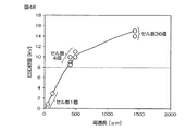
図7は、同面積の基板上に形成するダイオードセルの大きさおよび/またはダイオードセルの個数を様々に設定して、pn接合領域の周囲長の合計(総延長)を異ならせた複数のサンプルについてESD耐量を測定した実験結果を示す。この実験結果から、pn接合領域の周囲長が長くなるほど、ESD耐量が大きくなることが分かる。4個以上のダイオードセルを基板上に形成した場合に、8キロボルトを超えるESD耐量を実現することができた。
FIG. 7 shows a plurality of samples in which the sizes of diode cells and / or the number of diode cells formed on a substrate of the same area are variously set to make the total of the peripheral lengths of pn junction regions different (total extension) The experimental result which measured the ESD tolerance amount about is shown. From this experimental result, it can be seen that the ESD tolerance increases as the perimeter of the pn junction region increases. When four or more diode cells were formed on the substrate, an ESD resistance exceeding 8 kilovolts could be realized.
次に、図8A〜図8Hを参照して、チップ部品1の製造方法について詳説する。
まず、図8Aに示すように、基板2の元となるp+型の基板30を用意する。この場合、基板30の表面30Aは、基板2の素子形成面2Aであり、基板30の裏面30Bは、基板2の裏面2Bである。この基板30の表面30A側に、ダイオードセルD101〜D104が単位素子として、互いに間隔を空けて複数形成される。
Next, the method of manufacturing the chip part 1 will be described in detail with reference to FIGS. 8A to 8H.
First, as shown in FIG. 8A, a p + -type substrate 30 to be a source of the substrate 2 is prepared. In this case, the front surface 30A of the substrate 30 is the element forming surface 2A of the substrate 2, and the back surface 30B of the substrate 30 is the back surface 2B of the substrate 2. A plurality of diode cells D101 to D104 are formed as unit elements at intervals from each other on the surface 30A side of the substrate 30.
基板30を用意した後、基板30の表面に熱酸化膜等の絶縁膜115が形成され、その上にレジストマスクを形成する。このレジストマスクを介するn型不純物(たとえば燐)のイオン注入または拡散によって、n+型領域110が形成される。さらに、p+型領域112に整合する開口を有する別のレジストマスクが形成され、このレジストマスクを介するp型不純物(たとえば砒素)のイオン注入または拡散によって、p+型領域112が形成される。これにより、ダイオードセルD101〜D104が形成される。
After preparing the substrate 30, an insulating film 115 such as a thermal oxide film is formed on the surface of the substrate 30, and a resist mask is formed thereon. By ion implantation or diffusion of n-type impurities (for example, phosphorus) through the resist mask, n + -type region 110 is formed. Furthermore, another resist mask having openings matching the p + -type region 112 is formed, by ion implantation or diffusion of p-type impurity via the resist mask (eg arsenic), p + -type region 112 is formed. Thus, diode cells D101 to D104 are formed.
レジストマスクを剥離し、必要に応じて絶縁膜115を厚膜化(たとえばCVDにより厚膜化)した後、コンタクト孔116,117に整合する開口を有するさらに別のレジストマスクが絶縁膜115の上に形成される。このレジストマスクを介するエッチングによって、絶縁膜115にコンタクト孔116,117が形成される。
次に、図8Bに示すように、たとえばスパッタリングによって、カソード電極膜103およびアノード電極膜104を構成する電極膜が絶縁膜115上に形成される。そして、この電極膜上に、スリット118に対応する開口パターンを有するレジスト膜が形成され、このレジスト膜を介するエッチングによって、電極膜にスリット118が形成される。これにより、前記電極膜がカソード電極膜103およびアノード電極膜104に分離される。
After removing the resist mask and thickening the insulating film 115 as required (for example, by CVD), another resist mask having an opening aligned with the contact holes 116 and 117 is on the insulating film 115. Is formed. Contact holes 116 and 117 are formed in the insulating film 115 by etching through the resist mask.
Next, as shown in FIG. 8B, an electrode film constituting the cathode electrode film 103 and the anode electrode film 104 is formed on the insulating film 115 by sputtering, for example. Then, a resist film having an opening pattern corresponding to the slits 118 is formed on the electrode film, and the slits 118 are formed in the electrode film by etching through the resist film. Thereby, the electrode film is separated into the cathode electrode film 103 and the anode electrode film 104.
次に、図8Cに示すように、レジスト膜を剥離した後、たとえばCVD法によって窒化膜(SiN膜)等のパッシベーション膜23が形成され、さらにポリイミド等を塗布することにより樹脂膜24が形成される。そして、これらのパッシベーション膜23および樹脂膜24に対して、フォトリソグラフィを利用したエッチングを施すことにより、切欠部122,123が形成される。
Next, as shown in FIG. 8C, after peeling off the resist film, a passivation film 23 such as a nitride film (SiN film) is formed by, eg, CVD method, and a resin film 24 is formed by applying polyimide or the like. Ru. Then, the passivation film 23 and the resin film 24 are etched using photolithography to form the notches 122 and 123.
次に、図8Dに示すように、基板30の表面30Aの全域に亘ってレジストパターン41を形成する。レジストパターン41には、後述する溝45および貫通孔用の溝46を形成すべき領域に、開口42と、開口43とが選択的に形成されている。
図9は、図8Dの工程において溝45および貫通孔用の溝46を形成するために用いられるレジストパターン41の一部の模式的な平面図である。なお、図9では、説明の便宜上、レジストパターン41が形成された領域をクロスハッチングで示している。
Next, as shown in FIG. 8D, a resist pattern 41 is formed across the entire surface 30A of the substrate 30. In the resist pattern 41, an opening 42 and an opening 43 are selectively formed in a region where a groove 45 and a groove 46 for a through hole to be described later are to be formed.
FIG. 9 is a schematic plan view of a portion of a resist pattern 41 used to form the groove 45 and the through hole groove 46 in the process of FIG. 8D. In FIG. 9, for the convenience of description, the region in which the resist pattern 41 is formed is indicated by cross hatching.
図9を参照して、レジストパターン41の開口42は、直線部分42A,42Bを含む。直線部分42A,42Bは、平面視で互いに隣り合うダイオードセルD101〜D104を含む領域が平面視格子状に配列されるように、互いに直交した状態を保ちながらつながっている。つまり、直線部分42A,42Bは、ダイオードセルD101〜D104を含む領域を、チップ部品1となるチップ領域48として平面視格子状に区画している。
Referring to FIG. 9, opening 42 of resist pattern 41 includes straight portions 42A and 42B. The linear portions 42A and 42B are connected while maintaining a state of being orthogonal to each other so that regions including the diode cells D101 to D104 adjacent to each other in plan view are arranged in a grid in plan view. That is, the linear portions 42A and 42B divide the region including the diode cells D101 to D104 into a chip region 48 to be the chip part 1 in a lattice shape in plan view.
一方、開口43は、チップ領域48において、貫通孔用の溝46(貫通孔6)を形成すべき領域を選択的に露出させるように形成されている。
次に、図8Eに示すように、レジストパターン41をマスクとするプラズマエッチングにより、基板30を選択的に除去する。これにより、平面視においてレジストパターン41の開口42および開口43と一致する位置には、基板30の表面30Aから基板30の厚さ途中まで到達する所定深さの溝45および貫通孔用の溝46が形成される。溝45は、互いに対向する一対の側壁と、当該一対の側壁の下端(基板30の裏面30B側の端)の間を結ぶ底壁とによって区画されている。一方、貫通孔用の溝46は、4つの壁面と当該4つの壁面の下端(基板30の裏面30B側の端)の間を結ぶ底壁とによって区画されている。
On the other hand, the opening 43 is formed in the chip region 48 so as to selectively expose the region where the through hole groove 46 (through hole 6) is to be formed.
Next, as shown in FIG. 8E, the substrate 30 is selectively removed by plasma etching using the resist pattern 41 as a mask. Thereby, a groove 45 of a predetermined depth reaching the middle of the thickness of the substrate 30 from the surface 30A of the substrate 30 and a groove 46 for the through hole at the positions corresponding to the openings 42 and 43 of the resist pattern 41 in plan view. Is formed. The groove 45 is partitioned by a pair of side walls opposed to each other and a bottom wall connecting between the lower ends of the pair of side walls (the end on the back surface 30B side of the substrate 30). On the other hand, the through hole groove 46 is divided by the four wall surfaces and the bottom wall connecting the lower ends of the four wall surfaces (the end on the back surface 30B side of the substrate 30).
基板30における溝45および貫通孔用の溝46の全体形状は、平面視でレジストパターン41の開口42(直線部分42A,42B)および開口43と一致する形状になっている。基板30においてダイオードセルD101〜D104が形成された部分は、チップ部品1の半製品50である。基板30の表面30Aでは、溝45に区画された各チップ領域48に半製品50が1つずつ位置していて、これらの半製品50は、行列状に整列配置されている。溝45および貫通孔用の溝46が形成された後、レジストパターン41を除去する。レジストパターン41を除去した後、ダイオードセルD101〜D104のプロービング(電気テスト)を実施してもよい。
The overall shape of the groove 45 and the through hole groove 46 in the substrate 30 matches the opening 42 (straight portions 42A and 42B) and the opening 43 of the resist pattern 41 in a plan view. The portion of the substrate 30 where the diode cells D101 to D104 are formed is a semifinished product 50 of the chip part 1. On the surface 30A of the substrate 30, one semifinished product 50 is located in each chip area 48 partitioned in the groove 45, and these semifinished products 50 are arranged in a matrix. After the groove 45 and the through hole groove 46 are formed, the resist pattern 41 is removed. After removing the resist pattern 41, probing (electrical test) of the diode cells D101 to D104 may be performed.
次に、図8Fに示すように、CVD法によって、SiNからなる絶縁膜47を、基板30の表面30Aの全域に亘って形成する。このとき、溝45および貫通孔用の溝46の内周面(前述した側壁や底壁)の全域にも絶縁膜47が形成される。次に、溝45および貫通孔用の溝46の内周面以外の領域に形成された絶縁膜47を選択的にエッチングする。
次に、図8Gに示すように、図10に示す工程によって、各切欠部122,123から露出したカソードパッド105およびアノードパッド106(カソード電極膜103およびアノード電極膜104)からNi、PdおよびAuを順にめっき成長させる。めっきは、各めっき膜が表面30Aに沿う横方向に成長し、溝45および貫通孔用の溝46の側壁上の絶縁膜47を覆うまで続けられる。これにより、Ni/Pd/Au積層膜からなる第1および第2接続電極3,4を形成する。
Next, as shown in FIG. 8F, the insulating film 47 made of SiN is formed over the entire surface 30A of the substrate 30 by the CVD method. At this time, the insulating film 47 is also formed on the entire area of the inner peripheral surface (the side wall and the bottom wall described above) of the groove 45 and the through hole groove 46. Next, the insulating film 47 formed in the region other than the inner peripheral surface of the groove 45 and the through hole groove 46 is selectively etched.
Next, as shown in FIG. 8G, according to the process shown in FIG. 10, the cathode pad 105 and the anode pad 106 (the cathode electrode film 103 and the anode electrode film 104) exposed from the notches 122 and 123 are exposed to Ni, Pd and Au. The plating is grown in order. The plating is continued until each plating film grows in the lateral direction along the surface 30A and covers the insulating film 47 on the side walls of the groove 45 and the through hole groove 46. Thereby, the first and second connection electrodes 3 and 4 formed of the Ni / Pd / Au laminated film are formed.
図10は、第1および第2接続電極3,4の製造工程を説明するための図である。
まず、カソードパッド105およびアノードパッド106の表面が浄化されることで、当該表面の有機物(炭素のしみ等のスマットや油脂性の汚れも含む)が除去(脱脂)される(ステップS1)。次に、当該表面の酸化膜が除去される(ステップS2)。次に、当該表面においてジンケート処理が実施されて、当該表面における(電極膜の)AlがZnに置換される(ステップS3)。次に、当該表面上のZnが硝酸等で剥離されて、各パッド105,106では、新しいAlが露出される(ステップS4)。
FIG. 10 is a diagram for explaining the manufacturing process of the first and second connection electrodes 3 and 4.
First, by cleaning the surfaces of the cathode pad 105 and the anode pad 106, organic substances (including smut such as carbon stain and oily dirt) are removed (degreased) (step S1). Next, the oxide film on the surface is removed (step S2). Next, zincate treatment is performed on the surface, and Al (of the electrode film) on the surface is replaced with Zn (step S3). Next, Zn on the surface is exfoliated with nitric acid or the like, and new Al is exposed at each of the pads 105 and 106 (step S4).
次に、各パッド105,106をめっき液に浸けることによって、各パッド105,106における新しいAlの表面にNiめっきが施される。これにより、めっき液中のNiが化学的に還元析出されて、当該表面にNi層33が形成される(ステップS5)。
次に、Ni層33を別のめっき液に浸けることによって、当該Ni層33の表面にPdめっきが施される。これにより、めっき液中のPdが化学的に還元析出されて、当該Ni層33の表面にPd層34が形成される(ステップS6)。
Next, the new Al surface of each pad 105, 106 is Ni-plated by immersing each pad 105, 106 in a plating solution. Thereby, Ni in the plating solution is chemically reduced and deposited, and the Ni layer 33 is formed on the surface (step S5).
Next, the surface of the Ni layer 33 is plated with Pd by immersing the Ni layer 33 in another plating solution. Thereby, Pd in the plating solution is chemically reduced and deposited, and the Pd layer 34 is formed on the surface of the Ni layer 33 (step S6).
次に、Pd層34をさらに別のめっき液に浸けることによって、当該Pd層34の表面にAuめっきが施される。これにより、めっき液中のAuが化学的に還元析出されて、当該Pd層34の表面にAu層35が形成される(ステップS7)。これによって、第1および第2接続電極3,4が形成され、形成後の第1および第2接続電極3,4を乾燥させると(ステップS8)、第1および第2接続電極3,4の製造工程が完了する。なお、前後するステップの間には、半製品50を水で洗浄する工程が適宜実施される。また、ジンケート処理は複数回実施されてもよい。
Next, the surface of the Pd layer 34 is subjected to Au plating by immersing the Pd layer 34 in another plating solution. Thereby, Au in the plating solution is chemically reduced and deposited, and the Au layer 35 is formed on the surface of the Pd layer 34 (step S7). As a result, when the first and second connection electrodes 3 and 4 are formed, and the formed first and second connection electrodes 3 and 4 are dried (step S8), the first and second connection electrodes 3 and 4 are formed. The manufacturing process is complete. In addition, the process of wash | cleaning the semi-finished product 50 with water is suitably implemented between the steps which go back and forth. Also, the zincate treatment may be performed multiple times.
以上のように、第1および第2接続電極3,4を無電解めっきによって形成するので、電極材料であるNi,PdおよびAlを絶縁膜47上にも良好にめっき成長させることができる。また、第1および第2接続電極3,4を電解めっきによって形成する場合に比べて、第1および第2接続電極3,4についての形成工程の工程数(たとえば、電解めっきで必要となるリソグラフィ工程やレジストマスクの剥離工程等)を削減してチップ部品1の生産性を向上できる。さらに、無電解めっきの場合には、電解めっきで必要とされるレジストマスクが不要であることから、レジストマスクの位置ずれによる第1および第2接続電極3,4についての形成位置にずれが生じないので、第1および第2接続電極3,4の形成位置精度を向上して歩留まりを向上できる。
As described above, since the first and second connection electrodes 3 and 4 are formed by electroless plating, Ni, Pd and Al which are electrode materials can be plated and grown well on the insulating film 47. In addition, as compared with the case where the first and second connection electrodes 3 and 4 are formed by electrolytic plating, the number of steps for forming the first and second connection electrodes 3 and 4 (for example, lithography required for electrolytic plating) It is possible to improve the productivity of the chip part 1 by reducing the number of processes, the peeling process of the resist mask and the like. Furthermore, in the case of electroless plating, since the resist mask required for electrolytic plating is unnecessary, misalignment of the formation positions of the first and second connection electrodes 3 and 4 occurs due to misalignment of the resist mask. Since there is not, the formation position accuracy of the first and second connection electrodes 3 and 4 can be improved to improve the yield.
また、この方法では、カソードパッド105およびアノードパッド106(カソード電極膜103およびアノード電極膜104)が切欠部122,123から露出していて、各パッド105,106から溝45および貫通孔用の溝46までめっき成長の妨げになるものがない。そのため、各パッド105,106から溝45および貫通孔用の溝46まで直線的にめっき成長させることができる。その結果、電極の形成にかかる時間の短縮を図ることができる。
Further, in this method, the cathode pad 105 and the anode pad 106 (the cathode electrode film 103 and the anode electrode film 104) are exposed from the notches 122 and 123, and the grooves 45 and the through holes are formed from the respective pads 105 and 106. There is nothing up to 46 that prevents plating growth. Therefore, plating growth can be performed linearly from the pads 105 and 106 to the groove 45 and the through hole groove 46. As a result, the time taken to form the electrode can be shortened.
このように第1および第2接続電極3,4が形成された後に、基板30が裏面30Bから研削される。
具体的には、図8Hに示すように、溝45および貫通孔用の溝46を形成した後に、PET(ポリエチレンテレフタレート)からなる薄板状であって粘着面72を有する支持テープ71が、粘着面72において、各半製品50における第1および第2接続電極3,4側(つまり、表面30A)に貼着される。これにより、各半製品50が支持テープ71に支持される。ここで、支持テープ71として、たとえば、ラミネートテープを用いることができる。
After the first and second connection electrodes 3 and 4 are thus formed, the substrate 30 is ground from the back surface 30B.
Specifically, as shown in FIG. 8H, after forming the grooves 45 and the grooves 46 for the through holes, the support tape 71 which is a thin plate made of PET (polyethylene terephthalate) and has the adhesive surface 72 is an adhesive surface. At 72, the first and second connection electrodes 3 and 4 in each semifinished product 50 (ie, the surface 30A) are attached. Thereby, each semifinished product 50 is supported by the support tape 71. Here, as the support tape 71, for example, a laminate tape can be used.
各半製品50が支持テープ71に支持された状態で、基板30を裏面30B側から研削する。研削によって、溝45および貫通孔用の溝46の底壁の上面に達するまで基板30が薄型化されると、隣り合う半製品50を連結するものがなくなるので、溝45を境界として基板30が分割され、貫通孔用の溝46が基板2の貫通孔6として形成される。これにより、半製品50が個別に分離してチップ部品1の完成品となる。つまり、溝45および貫通孔用の溝46において基板30が切断(分断)され、これによって、貫通孔6を有する個々のチップ部品1が切り出される。なお、基板30を裏面30B側から溝45および貫通孔用の溝46の底壁までエッチングすることによってチップ部品1を切り出しても構わない。
With the semifinished products 50 supported by the support tape 71, the substrate 30 is ground from the back surface 30B side. When the substrate 30 is thinned until it reaches the upper surface of the bottom wall of the groove 45 and the groove 46 for through holes by grinding, there is no connection between the adjacent semi-finished products 50. Grooves 46 for the through holes are formed as the through holes 6 of the substrate 2. As a result, the semi-finished products 50 are separated individually and become finished products of the chip part 1. That is, the substrate 30 is cut (cut) in the groove 45 and the groove 46 for the through hole, whereby the individual chip parts 1 having the through hole 6 are cut out. The chip part 1 may be cut out by etching the substrate 30 from the back surface 30B to the groove 45 and the bottom wall of the groove 46 for the through hole.
完成した各チップ部品1では、溝45の側壁をなしていた部分が、基板2の側面2C〜2Fのいずれかとなり、また、貫通孔用の溝46の側壁をなしていた部分が、貫通孔6の壁面66となり、また、基板30の裏面30Bが裏面2Bとなる。つまり、エッチングによって溝45および貫通孔用の溝46を形成する工程(図8E参照)は、側面2C〜2F、および貫通孔6を形成する工程に含まれる。なお、溝45および貫通孔用の溝46に絶縁膜47の一部は、前述したパッシベーション膜23の一部となる。
In each completed chip part 1, the portion forming the side wall of the groove 45 is one of the side surfaces 2C to 2F of the substrate 2, and the portion forming the side wall of the groove 46 for the through hole is a through hole 6 and the back surface 30B of the substrate 30 is the back surface 2B. That is, the step of forming the grooves 45 and the through hole grooves 46 by etching (see FIG. 8E) is included in the steps of forming the side surfaces 2C to 2F and the through holes 6. A part of the insulating film 47 in the groove 45 and the through hole groove 46 is a part of the passivation film 23 described above.
以上のように、溝45および貫通孔用の溝46を形成してから基板30を裏面30B側から研削すれば、基板30に形成された複数のチップ部品1を一斉に個々に分割できる(複数のチップ部品1の個片を一度に得ることができる)とともに、貫通孔6を同時に形成できる。よって、複数のチップ部品1の製造時間の短縮によってチップ部品1の生産性の向上を図ることができる。
As described above, when the substrate 30 is ground from the back surface 30B side after the grooves 45 and the grooves 46 for through holes are formed, the plurality of chip components 1 formed on the substrate 30 can be divided simultaneously and individually (plurality The through hole 6 can be formed simultaneously with the individual pieces of the chip component 1 of (1). Therefore, the productivity of the chip component 1 can be improved by shortening the manufacturing time of the plurality of chip components 1.
なお、完成したチップ部品1における基板2の裏面2Bを研磨やエッチングすることによって鏡面化して裏面2Bを綺麗にしてもよい。むろん、完成したチップ部品1に対して、ダイオードセルD101〜D104のプロービング(電気テスト)を実施してもよい。
図11A〜図11Dは、図8Hの工程後におけるチップ部品1の回収工程を示す図解的な断面図である。
The back surface 2B of the completed chip part 1 may be mirror-finished by polishing or etching the back surface 2B to make the back surface 2B clear. Of course, probing (electrical test) of the diode cells D101 to D104 may be performed on the completed chip part 1.
11A to 11D are schematic sectional views showing the recovery step of the chip part 1 after the step of FIG. 8H.
図11Aでは、個片化された複数のチップ部品1が引き続き支持テープ71にくっついている状態を示している。この状態で、図11Bに示すように、各チップ部品1の基板2の裏面2Bに対して、熱発泡シート73を貼着する。熱発泡シート73は、シート状のシート本体74と、シート本体74内に練り込まれた多数の発泡粒子75とを含んでいる。
シート本体74の粘着力は、支持テープ71の粘着面72における粘着力よりも強い。そこで、各チップ部品1の基板2の裏面2Bに熱発泡シート73を貼着した後に、図11Cに示すように、支持テープ71を各チップ部品1から引き剥がして、チップ部品1を熱発泡シート73に転写する。このとき、支持テープ71に紫外線を照射すると(図11Bの点線矢印参照)、粘着面72の粘着性が低下するので、支持テープ71が各チップ部品1から剥がれやすくなる。
FIG. 11A shows a state in which a plurality of singulated chip parts 1 continue to be attached to the support tape 71. In this state, as shown in FIG. 11B, the thermally foamable sheet 73 is attached to the back surface 2B of the substrate 2 of each chip part 1. The thermally foamable sheet 73 includes a sheet-like sheet body 74 and a large number of foam particles 75 kneaded in the sheet body 74.
The adhesive force of the sheet main body 74 is stronger than the adhesive force of the adhesive surface 72 of the support tape 71. Therefore, after the thermally foamed sheet 73 is attached to the back surface 2B of the substrate 2 of each chip part 1, as shown in FIG. 11C, the support tape 71 is peeled off from each chip part 1, and the chip part 1 is thermally foamed sheet Transfer to 73. At this time, when the support tape 71 is irradiated with ultraviolet light (see the dotted arrow in FIG. 11B), the adhesion of the adhesive surface 72 is reduced, so the support tape 71 is easily peeled off from each chip part 1.
次に、熱発泡シート73を加熱する。これにより、図11Dに示すように、熱発泡シート73では、シート本体74内の各発泡粒子75が発泡してシート本体74の表面から膨出する。その結果、熱発泡シート73と各チップ部品1の基板2の裏面2Bとの接触面積が小さくなり、全てのチップ部品1が熱発泡シート73から自然に剥がれる(脱落する)。このように回収されたチップ部品1は、エンボスキャリアテープ(図示せず)に形成された収容空間に収容される。この場合、支持テープ71または熱発泡シート73からチップ部品1を1つずつ引き剥がす場合に比べて、処理時間の短縮を図ることができる。もちろん、複数のチップ部品1が支持テープ71にくっついた状態で(図11A参照)、熱発泡シート73を用いずに、支持テープ71からチップ部品1を所定個数ずつ直接引き剥がしてもよい。チップ部品1が収容されたエンボスキャリアテープは、その後、自動実装機に収納される。チップ部品1は、自動実装機に備えられた吸着ノズル76により吸着されて個々回収され、その後、実装基板9に実装される。
Next, the thermally foamable sheet 73 is heated. Thus, as shown in FIG. 11D, in the thermally foamable sheet 73, the foam particles 75 in the sheet main body 74 foam and expand from the surface of the sheet main body 74. As a result, the contact area between the thermally foamable sheet 73 and the back surface 2B of the substrate 2 of each chip part 1 becomes smaller, and all the chip parts 1 are naturally peeled off (dropped off) from the thermally foamable sheet 73. The chip part 1 collected in this manner is accommodated in the accommodation space formed in the embossed carrier tape (not shown). In this case, the processing time can be shortened compared to the case where the chip component 1 is peeled off one by one from the support tape 71 or the thermally foamable sheet 73. Of course, in a state where the plurality of chip parts 1 are attached to the support tape 71 (see FIG. 11A), a predetermined number of chip parts 1 may be directly peeled off from the support tape 71 without using the thermally foamable sheet 73. The embossed carrier tape in which the chip part 1 is accommodated is then accommodated in an automatic mounting machine. The chip parts 1 are sucked and collected individually by the suction nozzle 76 provided in the automatic mounting machine, and then mounted on the mounting substrate 9.
各チップ部品1の回収工程は、図12A〜図12Cに示す別の方法によっても行うことができる。
図12A〜図12Cは、図8Hの工程後におけるチップ部品1の回収工程(変形例)を示す図解的な断面図である。
図12Aでは、図11Aと同様に、個片化された複数のチップ部品1が引き続き支持テープ71にくっついている状態を示している。この状態で、図12Bに示すように、各チップ部品1の基板2の裏面2Bに転写テープ77を貼着する。転写テープ77は、支持テープ71の粘着面72よりも強い粘着力を有する。そこで、図12Cに示すように、各チップ部品1に転写テープ77を貼着した後に、支持テープ71を各チップ部品1から引き剥がす。この際、前述したように、粘着面72の粘着性を低下させるために支持テープ71に紫外線(図12Bの点線矢印参照)を照射してもよい。
The recovery step of each chip part 1 can also be performed by another method shown in FIGS. 12A to 12C.
12A to 12C are schematic sectional views showing the recovery step (modified example) of the chip part 1 after the step of FIG. 8H.
In FIG. 12A, as in FIG. 11A, a state in which a plurality of singulated chip components 1 is continuously attached to the support tape 71 is shown. In this state, as shown in FIG. 12B, a transfer tape 77 is attached to the back surface 2B of the substrate 2 of each chip part 1. The transfer tape 77 has a stronger adhesive force than the adhesive surface 72 of the support tape 71. Therefore, as shown in FIG. 12C, after the transfer tape 77 is attached to each chip part 1, the support tape 71 is peeled off from each chip part 1. At this time, as described above, in order to reduce the adhesiveness of the adhesive surface 72, the support tape 71 may be irradiated with ultraviolet light (see the dotted arrow in FIG. 12B).
転写テープ77の両端には、自動実装機に設置されたフレーム78が貼り付けられている。両側のフレーム78は、互いが接近する方向または離間する方向に移動できる。支持テープ71を各チップ部品1から引き剥がした後に、両側のフレーム78を互いが離間する方向に移動させると、転写テープ77が伸張して薄くなる。これによって、転写テープ77の粘着力が低下するので、各チップ部品1が転写テープ77から剥がれやすくなる。この状態で、自動実装機の吸着ノズル76をチップ部品1の素子形成面2A側に向けると、自動実装機(吸着ノズル76)が発生する吸着力によって、チップ部品1が転写テープ77から引き剥がされて吸着ノズル76に吸着される。この際、図12Cに示す突起79によって、吸着ノズル76とは反対側から転写テープ77越しにチップ部品1を吸着ノズル76側へ突き上げると、チップ部品1を転写テープ77から円滑に引き剥がすことができる。
At both ends of the transfer tape 77, a frame 78 installed in an automatic mounting machine is attached. The frames 78 on both sides can move in a direction toward or away from each other. After peeling the support tape 71 from each chip part 1, when the frames 78 on both sides are moved in a direction away from each other, the transfer tape 77 is stretched and thinned. As a result, the adhesive force of the transfer tape 77 is reduced, so that each chip part 1 is easily peeled off from the transfer tape 77. In this state, when the suction nozzle 76 of the automatic mounting machine is directed to the element forming surface 2A side of the chip part 1, the chip part 1 is peeled off from the transfer tape 77 by the adsorption force generated by the automatic mounting machine (suction nozzle 76). It is absorbed by the suction nozzle 76. At this time, if the chip component 1 is pushed up to the suction nozzle 76 side from the opposite side to the suction nozzle 76 through the transfer tape 77 by the projection 79 shown in FIG. 12C, the chip component 1 can be smoothly pulled off from the transfer tape 77. it can.
図13は、チップ部品1が実装基板9に実装された状態の回路アセンブリ100をチップ部品1の長手方向に沿って切断したときの模式的な断面図である。図14は、実装基板9に実装された状態のチップ部品1を素子形成面2A側から見た模式的な平面図である。
図13に示すように、チップ部品1は、実装基板9に実装される。この状態におけるチップ部品1および実装基板9は、回路アセンブリ100を構成している。図13における実装基板9の上面は、実装面9Aである。実装面9Aには、実装基板9の内部回路(図示せず)に接続された一対(2つ)のランド88が形成されている。各ランド88は、たとえば、Cuからなる。各ランド88の表面には、はんだ13が当該表面から突出するように設けられている。
FIG. 13 is a schematic cross-sectional view of the circuit assembly 100 in a state in which the chip component 1 is mounted on the mounting substrate 9, cut along the longitudinal direction of the chip component 1. FIG. 14 is a schematic plan view of the chip component 1 mounted on the mounting substrate 9 as viewed from the element forming surface 2A.
As shown in FIG. 13, the chip component 1 is mounted on the mounting substrate 9. The chip component 1 and the mounting substrate 9 in this state constitute a circuit assembly 100. The upper surface of the mounting substrate 9 in FIG. 13 is a mounting surface 9A. On the mounting surface 9A, a pair (two) of lands 88 connected to an internal circuit (not shown) of the mounting substrate 9 is formed. Each land 88 is made of, for example, Cu. The solder 13 is provided on the surface of each land 88 so as to protrude from the surface.
自動実装機は、チップ部品1を吸着した状態で吸着ノズル76を実装基板9まで移動させる。このとき、吸着ノズル76は、裏面2Bの長手方向における略中央部分に吸着する。前述したように、第1および第2接続電極3,4は、チップ部品1の片面(素子形成面2A)および側面2C〜2Fにおける素子形成面2A側の端部だけに設けられており、かつ基板2の貫通孔6は、チップ部品1の略中央部分を避けた位置に形成されている。したがって、基板2の裏面2Bの略中央部分には、第1および第2接続電極3,4および貫通孔6(凹凸)がない平坦面(吸着ノズル76によって吸着される平坦な吸着面)が形成されている。
The automatic mounting machine moves the suction nozzle 76 to the mounting substrate 9 in a state where the chip component 1 is suctioned. At this time, the suction nozzle 76 sucks at a substantially central portion in the longitudinal direction of the back surface 2B. As described above, the first and second connection electrodes 3 and 4 are provided only at one end (element forming surface 2A) of the chip part 1 and the end on the element forming surface 2A side of the side surfaces 2C to 2F, The through hole 6 of the substrate 2 is formed at a position avoiding the substantially central portion of the chip part 1. Therefore, a flat surface (flat suction surface adsorbed by suction nozzle 76) free of first and second connection electrodes 3 and 4 and through holes 6 (concave and convex) is formed substantially at the center of back surface 2B of substrate 2. It is done.
よって、吸着ノズル76をチップ部品1に吸着して移動させる場合に、平坦な裏面2Bに吸着ノズル76を吸着させることができる。換言すれば、平坦な裏面2Bであれば、吸着ノズル76が吸着できる部分のマージンを増やすことができる。これによって、吸着ノズル76をチップ部品1に確実に吸着させ、チップ部品1を途中で吸着ノズル76から脱落させることなく実装基板9上まで搬送できる。実装基板9上では、チップ部品1の素子形成面2Aと実装基板9の実装面9Aとが互いに対向する。この状態で、吸着ノズル76を下降させて実装基板9に押し付け、チップ部品1において、第1接続電極3を一方のランド88のはんだ13に接触させ、第2接続電極4を他方のランド88のはんだ13に接触させる。
Therefore, when the suction nozzle 76 is moved by suction to the chip part 1, the suction nozzle 76 can be sucked by the flat back surface 2B. In other words, in the case of the flat back surface 2B, the margin of the portion to which the suction nozzle 76 can suction can be increased. As a result, the suction nozzle 76 can be reliably suctioned to the chip part 1, and the chip part 1 can be transported onto the mounting substrate 9 without being dropped from the suction nozzle 76 on the way. On the mounting substrate 9, the element forming surface 2A of the chip part 1 and the mounting surface 9A of the mounting substrate 9 face each other. In this state, the suction nozzle 76 is lowered and pressed against the mounting substrate 9, and in the chip part 1, the first connection electrode 3 is brought into contact with the solder 13 of one land 88 and the second connection electrode 4 is made of the other land 88. Contact the solder 13.
次に、リフロー工程により、はんだ13を加熱すると、はんだ13が溶融する。その後、はんだ13が冷却されて固まると、第1接続電極3と当該一方のランド88とがはんだ13を介して接合し、第2接続電極4と当該他方のランド88とがはんだ13を介して接合する。つまり、二つのランド88のそれぞれが、第1および第2接続電極3,4において対応する電極にはんだ接合される。これにより、実装基板9へのチップ部品1の実装(フリップチップ接続)が完了して、回路アセンブリ100が完成する。このとき、チップ部品1の外部接続電極として機能する第1および第2接続電極3,4の最表面には、Au層35(金メッキ)が形成されている。そのため、チップ部品1を実装基板9に実装する際に、優れたはんだ濡れ性と、高い信頼性とを達成できる。
Next, when the solder 13 is heated by a reflow process, the solder 13 is melted. Thereafter, when the solder 13 is cooled and solidified, the first connection electrode 3 and the one land 88 are joined via the solder 13, and the second connection electrode 4 and the other land 88 via the solder 13. Join. That is, each of the two lands 88 is soldered to the corresponding electrode at the first and second connection electrodes 3 and 4. Thereby, the mounting (flip chip connection) of the chip component 1 on the mounting substrate 9 is completed, and the circuit assembly 100 is completed. At this time, an Au layer 35 (gold plating) is formed on the outermost surfaces of the first and second connection electrodes 3 and 4 which function as the external connection electrodes of the chip part 1. Therefore, when the chip component 1 is mounted on the mounting substrate 9, excellent solder wettability and high reliability can be achieved.
完成状態の回路アセンブリ100では、チップ部品1の素子形成面2Aと実装基板9の実装面9Aとが、隙間を隔てて対向しつつ、平行に延びている(図14も参照)。当該隙間の寸法は、第1接続電極3または第2接続電極4において素子形成面2Aから突き出た部分の厚みとはんだ13の厚さとの合計に相当する。
図13に示すように、断面視においては、たとえば、第1および第2接続電極3,4は、素子形成面2A上の表面部分と側面2C〜2F上の側面部分とが一体的になって略L字状に形成されている。そのため、図14に示すように、実装面9A(素子形成面2A)の法線方向(これらの面に直交する方向)から回路アセンブリ100(厳密には、チップ部品1と実装基板9との接合部分)を見てみると、第1接続電極3と一方のランド88とを接合するはんだ13は、第1接続電極3の表面部分だけでなく、側面部分にも吸着している。同様に、第2接続電極4と他方のランド88とを接合するはんだ13も、第2接続電極4の表面部分だけでなく、側面部分にも吸着している。
In the completed circuit assembly 100, the element forming surface 2A of the chip part 1 and the mounting surface 9A of the mounting substrate 9 extend in parallel, facing each other with a gap (see also FIG. 14). The dimension of the gap corresponds to the sum of the thickness of the portion of the first connection electrode 3 or the second connection electrode 4 protruding from the element formation surface 2A and the thickness of the solder 13.
As shown in FIG. 13, in cross section, for example, the first and second connection electrodes 3 and 4 have the surface portion on the element forming surface 2A and the side portions on the side surfaces 2C to 2F integrated. It is formed in a substantially L-shape. Therefore, as shown in FIG. 14, the circuit assembly 100 (strictly speaking, bonding of the chip component 1 and the mounting substrate 9 from the normal direction (direction orthogonal to these surfaces) of the mounting surface 9A (element forming surface 2A) When looking at the part), the solder 13 joining the first connection electrode 3 and the one land 88 is adsorbed not only to the surface part of the first connection electrode 3 but also to the side part. Similarly, the solder 13 for joining the second connection electrode 4 and the other land 88 is also adsorbed not only to the surface portion of the second connection electrode 4 but also to the side surface portion.
このように、チップ部品1では、第1接続電極3が基板2の側面2C,2E,2Fを一体的に覆うように形成され、第2接続電極4が基板2の側面2D,2E,2Fを一体的に覆うように形成されている。すなわち、基板2の素子形成面2Aに加えて側面2C〜2Fにも電極が形成されているので、チップ部品1を実装基板9にはんだ付けする際の接着面積を拡大できる。その結果、第1および第2接続電極3,4に対するはんだ13の吸着量を増やすことができるので、接着強度を向上させることができる。
As described above, in the chip part 1, the first connection electrode 3 is formed to integrally cover the side surfaces 2C, 2E, 2F of the substrate 2, and the second connection electrode 4 is formed as the side surfaces 2D, 2E, 2F of the substrate 2. It is formed to cover integrally. That is, since the electrodes are formed on the side surfaces 2C to 2F in addition to the element forming surface 2A of the substrate 2, the bonding area when soldering the chip component 1 to the mounting substrate 9 can be expanded. As a result, since the amount of adsorption of the solder 13 to the first and second connection electrodes 3 and 4 can be increased, the adhesive strength can be improved.
また、図14に示すように、はんだ13が基板2の素子形成面2Aから側面2C〜2Fに回り込むように吸着する。したがって実装状態において、第1接続電極3を側面2C,2E,2Fではんだ13によって保持し、第2接続電極4を側面2D,2E,2Fではんだ13によって保持することによって、矩形状のチップ部品1の全ての側面2C〜2Fをはんだ13で固定できる。これにより、チップ部品1の実装形状を安定化させることができる。
Further, as shown in FIG. 14, the solder 13 is attracted so as to wrap around from the element forming surface 2A of the substrate 2 to the side surfaces 2C to 2F. Therefore, in the mounted state, the rectangular chip component is held by holding the first connection electrode 3 by the solder 13 on the side surfaces 2C, 2E, 2F and holding the second connection electrode 4 by the solder 13 on the side surfaces 2D, 2E, 2F. All side surfaces 2C to 2F of 1 can be fixed by the solder 13. Thereby, the mounting shape of the chip component 1 can be stabilized.
チップ部品1が実装基板9に実装された回路アセンブリ100は、基板外観検査工程を経て「良品」と判定されたものだけが出荷される。基板外観検査工程では、検査装置としての自動光学検査装置(AOI:Automatic Optical Inspection Machine)91によって、判定項目として、実装基板9のはんだ付けの状態検査、チップ部品1の極性検査等が実施される。
As for the circuit assembly 100 in which the chip part 1 is mounted on the mounting substrate 9, only those which are judged as "non-defective products" after the board appearance inspection process are shipped. In the board appearance inspection step, the inspection condition of the soldering of the mounting substrate 9, the polarity inspection of the chip part 1, etc. are performed as determination items by an automatic optical inspection machine (AOI) 91 as an inspection device. .
図15は、図1に示すチップ部品1の極性検査工程を説明するための図である。図16は、実装基板9に実装された状態の参考例に係るチップ部品10を裏面2B側から見た模式的な平面図である。なお、図15は、チップ部品1が実装基板9に実装された状態の回路アセンブリ100をチップ部品1の長手方向に沿って切断したときの模式的な断面図を示している。
FIG. 15 is a diagram for explaining a polarity inspection process of the chip part 1 shown in FIG. FIG. 16 is a schematic plan view of the chip part 10 according to the reference example mounted on the mounting substrate 9 as viewed from the back surface 2B side. FIG. 15 is a schematic cross-sectional view of the circuit assembly 100 in a state in which the chip part 1 is mounted on the mounting substrate 9, cut along the longitudinal direction of the chip part 1.
自動光学検査装置91は、検査対象物に光を照射し、検査対象物から反射された光によって検出された映像情報から「良品」、「不良品」を判定する装置である。より具体的に、図15に示すように、自動光学検査装置91における部品検出位置Pでは、回路アセンブリ100の直上に部品認識カメラ14と、複数の光源15とが配置されている。複数の光源15は、当該部品認識カメラ14の周囲にそれぞれ配置されている。回路アセンブリ100が部品検出位置Pに載置されると、自動光学検査装置91は、光源15からチップ部品1の裏面2Bに向けて光を斜め方向に照射し、そして、当該チップ部品1の裏面2Bによって反射された反射光を部品認識カメラ14によって検出する。
The automatic optical inspection device 91 is a device that irradiates light to the inspection object and determines “non-defective product” and “defective product” from the image information detected by the light reflected from the inspection object. More specifically, as shown in FIG. 15, at the component detection position P in the automatic optical inspection apparatus 91, a component recognition camera 14 and a plurality of light sources 15 are disposed immediately above the circuit assembly 100. The plurality of light sources 15 are respectively disposed around the component recognition camera 14. When the circuit assembly 100 is placed at the component detection position P, the automatic optical inspection device 91 obliquely emits light from the light source 15 toward the back surface 2 B of the chip component 1, and the back surface of the chip component 1. The reflected light reflected by 2 B is detected by the component recognition camera 14.
ここで、図16に示すように、参考例に係るチップ部品10には、基板2に貫通孔6が形成されておらず、裏面2Bに標印としてのアノードマークAM2が形成(印字)されている。このような標印は、チップ部品10の裏面2Bに紫外線やレーザ等を照射する標印装置によって形成されている。
参考例に係るチップ部品10の極性検査は、たとえば、アノードマークAM2(標印)が、自動光学検査装置91の所定位置にある極性検査ウィンドウに予め設定された値以上の色(たとえば、白色や水色等)で検出されるか否かによって行われ、検出された場合に「良品」と判定される。
Here, as shown in FIG. 16, in the chip part 10 according to the reference example, the through hole 6 is not formed in the substrate 2, and the anode mark AM2 as a mark is formed (printed) on the back surface 2B. There is. Such a mark is formed by a marking device that irradiates the back surface 2B of the chip part 10 with ultraviolet light, a laser or the like.
For the polarity inspection of the chip part 10 according to the reference example, for example, a color (for example, white or more) having a value equal to or more than a value preset in the polarity inspection window where the anode mark AM2 It is performed depending on whether or not it is detected in light blue etc., and when it is detected, it is determined to be "good."
しかしながら、参考例に係るチップ部品10は、必ずしも水平な姿勢で実装基板9に実装されるわけではなく、時には傾いた姿勢で実装基板9に実装される場合がある。この場合、その傾斜角度によっては、光源15から参考例に係るチップ部品10に照射された光の一部が極性検査ウィンドウ外に反射したり、入射光に対する反射光の波長が変化し、検出される色が設定値以下の色として認識(誤認識)されたりすることがある。その結果、第1および第2接続電極3,4の極性方向が誤っていないにも関わらず、「不良品」と判定されるという不具合がある。このような問題は、参考例に係るチップ部品10の裏面2Bの鏡面性が高いほど顕著になる。
However, the chip component 10 according to the reference example is not necessarily mounted on the mounting substrate 9 in a horizontal posture, and sometimes may be mounted on the mounting substrate 9 in an inclined posture. In this case, depending on the tilt angle, a part of the light emitted from the light source 15 to the chip part 10 according to the reference example may be reflected out of the polarity inspection window, or the wavelength of the reflected light with respect to the incident light may be changed. May be recognized (misrecognized) as a color below the set value. As a result, there is a problem that the first and second connection electrodes 3 and 4 are determined as “defective products” even though the polarity directions are not erroneous. Such a problem becomes remarkable as the specularity of the back surface 2B of the chip part 10 according to the reference example increases.
このような誤認識を防止するためには、自動光学検査装置91の検出系統(部品認識カメラ14等)や照明系統(光源15等)を検査対象物毎に最適化して検査精度を上げなければならず、外観検査のために余計な労力が必要になって生産性が低下する。しかも、今後益々小型のチップ部品が要望されるようになると、その労力が過大になってしまう。
これに対して、本発明に係るチップ部品1には、図1および図2に示すように、基板2には、アノードマークAM1としての貫通孔6が形成されている。そのため、チップ部品1が実装基板9に実装された際に、貫通孔6の位置に基づいて第1および第2接続電極3,4のそれぞれの位置を確認することができる。これにより、第1および第2接続電極3,4の極性方向を簡単に判定することができる。しかも、その極性判定は、自動光学検査装置91で検出される明るさや色合いに基づいて行われるものではなく、実装基板9に対するチップ部品1の傾きが変わっても不変な貫通孔6の形状に基づいて行われる。したがって、極性検査工程において、たとえチップ部品1が傾いた姿勢で実装された実装基板9や、水平な姿勢で実装された実装基板9が混在する場合であっても、貫通孔6(貫通孔6の外観形状)に基づくことによって、実装基板9毎に自動光学検査装置91の検出系統(部品認識カメラ14等)を最適化することなしに、安定した品質で極性方向を判定することができる。
In order to prevent such false recognition, it is necessary to optimize the detection system (the component recognition camera 14 etc.) and the illumination system (the light source 15 etc.) of the automatic optical inspection apparatus 91 for each inspection object to increase inspection accuracy. In addition, extra labor is required for appearance inspection, which reduces productivity. In addition, if the demand for smaller chip components is increased in the future, the labor will be excessive.
On the other hand, in the chip part 1 according to the present invention, as shown in FIG. 1 and FIG. 2, the through hole 6 as the anode mark AM1 is formed in the substrate 2. Therefore, when the chip component 1 is mounted on the mounting substrate 9, the positions of the first and second connection electrodes 3 and 4 can be confirmed based on the positions of the through holes 6. Thereby, the polarity directions of the first and second connection electrodes 3 and 4 can be easily determined. Moreover, the polarity determination is not performed based on the brightness or the color tone detected by the automatic optical inspection device 91, but based on the shape of the through hole 6 which is invariant even if the inclination of the chip part 1 with respect to the mounting substrate 9 changes. Be done. Therefore, even in the case where the mounting substrate 9 on which the chip component 1 is mounted in an inclined posture and the mounting substrate 9 mounted on a horizontal posture coexist in the polarity inspection step, the through holes 6 (through holes 6 Based on the appearance shape of (1), the polarity direction can be determined with stable quality without optimizing the detection system (such as the component recognition camera 14) of the automatic optical inspection device 91 for each mounting substrate 9.
また、極性方向を判定するための指標として、チップ部品の表面や裏面に標印を形成する必要がないため、紫外線やレーザ等の照射によってチップ部品に標印を形成するための標印装置を使用する必要もない。そのため、チップ部品の製造工程を簡略化できるとともに、設備投資を削減できる。これにより、生産性の向上を図ることもできる。
また、チップ部品1の裏面2Bの鏡面性を高くしても、自動光学検査装置91から裏面2Bに入射した光を効率よく反射させることができる。そのため、実装基板9に対するチップ部品1の傾き具合が異なる様々な実装基板9を検査する場合に、ある傾きを他の傾きと区別するための情報(反射光の明るさや色合い)を、自動光学検査装置91に良好に反映させることができる。その結果、チップ部品1の傾きを良好に検出することができる。とくに、本発明では、極性方向の判定の指標としてチップ部品1からの反射光の情報を省略できるので、このような裏面2Bの鏡面化によってチップ部品1の極性方向の判定精度が低下することを防止することができる。
In addition, since it is not necessary to form a mark on the front surface or the back surface of the chip component as an index for determining the polarity direction, a marking apparatus for forming a mark on the chip component by irradiation with ultraviolet light or laser There is no need to use it. Therefore, the manufacturing process of the chip part can be simplified and the equipment investment can be reduced. This can also improve productivity.
Further, even if the mirror surface property of the back surface 2B of the chip part 1 is increased, the light incident from the automatic optical inspection device 91 to the back surface 2B can be efficiently reflected. Therefore, when inspecting various mounting substrates 9 having different degrees of inclination of the chip component 1 with respect to the mounting substrate 9, automatic optical inspection of information (brightness and color of reflected light) for distinguishing one inclination from the other inclination It can be well reflected in the device 91. As a result, the inclination of the chip part 1 can be detected favorably. In particular, in the present invention, the information of the reflected light from the chip part 1 can be omitted as an index of the judgment of the polarity direction, so that the judgment accuracy of the polarity direction of the chip part 1 is lowered by the mirror surface of such back surface 2B. It can be prevented.
なお、チップ部品1を実装基板9に実装する際に、自動実装機等による表裏判定工程および極性判定工程を行ってもよい。この場合、チップ部品1には、互いに相異なる形状、面積を有する第1および第2接続電極3,4が形成されているので、第1および第2接続電極3,4の形状に基いて、チップ部品1の表裏判定および極性判定ができる。
以上のように、チップ部品1の構成によれば、生産性の低下を抑制しながら、極性方向を精度よく判定できるので、チップ部品1の極性方向に誤りがなく、信頼性の高い電子回路を有する回路アセンブリ100を提供できる。また、このような回路アセンブリ100を含む電子機器を提供できる。
<第2実施形態>
図17は、本発明の第2実施形態に係るチップ部品201の構成を説明するための平面図である。図18は、図17に示す切断面線XVIII−XVIIIから見た断面図である。
When the chip component 1 is mounted on the mounting substrate 9, the front / back determination process and the polarity determination process may be performed by an automatic mounting machine or the like. In this case, since the first and second connection electrodes 3 and 4 having shapes and areas different from each other are formed in the chip part 1, based on the shapes of the first and second connection electrodes 3 and 4, Front and back judgment and polarity judgment of the chip part 1 can be performed.
As described above, according to the configuration of the chip part 1, the polarity direction can be determined accurately while suppressing the decrease in productivity. Therefore, there is no error in the polarity direction of the chip part 1, and an electronic circuit with high reliability can be obtained. The circuit assembly 100 can be provided. In addition, an electronic device including such a circuit assembly 100 can be provided.
Second Embodiment
FIG. 17 is a plan view for explaining the configuration of the chip part 201 according to the second embodiment of the present invention. FIG. 18 is a cross-sectional view as seen from the section line XVIII-XVIII shown in FIG.
チップ部品201は、基板2と、基板2上に形成されたカソード電極膜233およびアノード電極膜234と、カソード電極膜233およびアノード電極膜234の間に並列に接続された複数のダイオードセルD201〜D204とを有している。基板2には、前述の第1実施形態と同様の構成で、貫通孔6が形成されている。
基板2の長手方向の両端部にカソードパッド235およびアノードパッド236がそれぞれ配置されている。これらのカソードパッド235およびアノードパッド236の間に矩形形状のダイオードセル領域237が設定されている。このダイオードセル領域237内に、複数のダイオードセルD201〜D204が二次元配列されている。本実施形態では、複数のダイオードセルD201〜D204は、基板2の長手方向および短手方向に沿ってマトリックス状に等間隔で配列されている。
The chip part 201 includes a substrate 2, a cathode electrode film 233 and an anode electrode film 234 formed on the substrate 2, and a plurality of diode cells D 201 connected in parallel between the cathode electrode film 233 and the anode electrode film 234. And D204. Through holes 6 are formed in the substrate 2 in the same configuration as that of the first embodiment described above.
Cathode pads 235 and anode pads 236 are respectively disposed at both ends in the longitudinal direction of the substrate 2. A rectangular shaped diode cell region 237 is set between the cathode pad 235 and the anode pad 236. In the diode cell area 237, a plurality of diode cells D201 to D204 are two-dimensionally arranged. In the present embodiment, the plurality of diode cells D <b> 201 to D <b> 204 are arranged at equal intervals in a matrix along the longitudinal direction and the short direction of the substrate 2.
ダイオードセルD201〜D204は、それぞれ矩形の領域からなり、その矩形の領域の内部に、平面視多角形形状(本実施形態では正八角形形状)のショットキ接合領域241を有している。各ショットキ接合領域241に接触するように、ショットキメタル240が配置されている。すなわち、ショットキメタル240は、ショットキ接合領域241において基板2にショットキ接合している。
Each of the diode cells D201 to D204 is formed of a rectangular area, and has a schottky junction area 241 having a polygonal shape in plan view (a regular octagonal shape in the present embodiment) inside the rectangular area. The Schottky metal 240 is disposed to be in contact with each Schottky junction region 241. That is, the Schottky metal 240 is in Schottky junction with the substrate 2 in the Schottky junction region 241.
基板2は、本実施形態では、p型シリコン基板250と、その上にエピタキシャル成長させられたn型エピタキシャル層251とを有している。基板2には、図18に示すように、p型シリコン基板250の表面に形成されたn型不純物(たとえば砒素)を導入して形成されたn+型埋め込み層252が形成されていてもよい。ショットキ接合領域241は、n型エピタキシャル層251の表面に設定されており、このn型エピタキシャル層251の表面にショットキメタル240が接合されることによって、ショットキ接合が形成されている。ショットキ接合領域241の周囲には、コンタクトエッジのリークを抑制するためのガードリング253が形成されている。
In the present embodiment, the substrate 2 has a p-type silicon substrate 250 and an n-type epitaxial layer 251 epitaxially grown thereon. In the substrate 2, as shown in FIG. 18, an n + -type buried layer 252 formed by introducing an n-type impurity (for example, arsenic) formed on the surface of the p-type silicon substrate 250 may be formed. . The Schottky junction region 241 is set on the surface of the n-type epitaxial layer 251, and the Schottky junction is formed on the surface of the n-type epitaxial layer 251 by the Schottky metal 240 being joined. A guard ring 253 is formed around the Schottky junction region 241 to suppress leakage of the contact edge.
ショットキメタル240は、たとえばTiまたはTiNからなっていてもよく、このショットキメタル240にAiSi合金等の金属膜242が積層されてカソード電極膜233が構成されている。ショットキメタル240は、ダイオードセルD201〜D204毎に分離されていてもよいが、本実施形態では、複数のダイオードセルD201〜D204の各ショットキ接合領域241に共通に接触するようにショットキメタル240が形成されている。
The Schottky metal 240 may be made of, for example, Ti or TiN, and a metal film 242 such as an AiSi alloy is laminated on the Schottky metal 240 to form a cathode electrode film 233. The Schottky metal 240 may be separated for each of the diode cells D201 to D204, but in the present embodiment, the Schottky metal 240 is formed to be in common contact with each of the Schottky junction regions 241 of the plurality of diode cells D201 to D204. It is done.
n型エピタキシャル層251には、ショットキ接合領域241を回避した領域に、n型エピタキシャル層251の表面からn+型埋め込み層252に達するn+型ウェル254が形成されている。そして、n+型ウェル254の表面との間でオーミック接触が形成されるようにアノード電極膜234が形成されている。アノード電極膜234は、カソード電極膜233と同様の構成の電極膜からなっていてもよい。
In the n-type epitaxial layer 251, an n + -type well 254 extending from the surface of the n-type epitaxial layer 251 to the n + -type embedded layer 252 is formed in a region avoiding the Schottky junction region 241. Then, an anode electrode film 234 is formed so as to form an ohmic contact with the surface of the n + -type well 254. The anode electrode film 234 may be made of an electrode film having the same configuration as that of the cathode electrode film 233.
n型エピタキシャル層251の表面には、絶縁膜115が形成されている。絶縁膜115には、ショットキ接合領域241に対応したコンタクト孔246と、n+型ウェル254を露出させるコンタクト孔247とが形成されている。カソード電極膜233は、絶縁膜115を覆うように形成されていて、コンタクト孔246の内部にまで達し、コンタクト孔246内においてn型エピタキシャル層251との間でショットキ接合を形成している。一方、アノード電極膜234は、絶縁膜115上に形成されていて、コンタクト孔247内に延び、このコンタクト孔247内においてn+型ウェル254にオーミック接触している。カソード電極膜233とアノード電極膜234とは、スリット248によって分離されている。
An insulating film 115 is formed on the surface of the n-type epitaxial layer 251. In the insulating film 115, a contact hole 246 corresponding to the Schottky junction region 241 and a contact hole 247 for exposing the n + -type well 254 are formed. The cathode electrode film 233 is formed so as to cover the insulating film 115, extends to the inside of the contact hole 246, and forms a Schottky junction with the n-type epitaxial layer 251 in the contact hole 246. On the other hand, the anode electrode film 234 is formed on the insulating film 115, extends into the contact hole 247, and is in ohmic contact with the n + -type well 254 in the contact hole 247. The cathode electrode film 233 and the anode electrode film 234 are separated by the slit 248.
パッシベーション膜23は、前述の第1実施形態と同様の構成で、素子形成面2A(カソード電極膜233およびアノード電極膜234上)および側面2C〜2F、ならびに貫通孔6の壁面66を覆うように形成されている。さらに、パッシベーション膜23を覆うように、樹脂膜24が形成されている。パッシベーション膜23および樹脂膜24を貫通して、カソードパッド235となるカソード電極膜233の表面の一部の領域を露出させる切欠部122が形成されている。さらに、パッシベーション膜23および樹脂膜24を貫通するように、アノードパッド236となるアノード電極膜234の表面の一部領域を露出させるように切欠部123が形成されている。そして、切欠部122,123から露出しているカソードパッド235およびアノードパッド236に、前述の第1実施形態と同様の構成で、第1および第2接続電極3,4が形成されている。
The passivation film 23 has the same configuration as that of the first embodiment described above, and covers the element formation surface 2A (on the cathode electrode film 233 and the anode electrode film 234) and the side surfaces 2C to 2F and the wall surface 66 of the through hole 6. It is formed. Furthermore, a resin film 24 is formed to cover the passivation film 23. A notch 122 is formed through the passivation film 23 and the resin film 24 to expose a partial region of the surface of the cathode electrode film 233 which is to be the cathode pad 235. Furthermore, a notch 123 is formed to penetrate the passivation film 23 and the resin film 24 so as to expose a partial region of the surface of the anode electrode film 234 which is to be the anode pad 236. The first and second connection electrodes 3 and 4 are formed on the cathode pad 235 and the anode pad 236 exposed from the notches 122 and 123 in the same configuration as the first embodiment described above.
このような構成によって、カソード電極膜233は、ダイオードセルD201〜D204がそれぞれ有するショットキ接合領域241に共通に接続されている。また、アノード電極膜234は、n+型ウェル254およびn+型埋め込み層252を介してn型エピタキシャル層251に接続されており、したがって、複数のダイオードセルD201〜D204に形成されたショットキ接合領域241に共通に並列接続されていることになる。これにより、複数のダイオードセルD201〜D204のショットキ接合領域241を有する複数のショットキバリアダイオードが、カソード電極膜233とアノード電極膜234との間に並列に接続されている。
With such a configuration, the cathode electrode film 233 is commonly connected to the Schottky junction regions 241 included in the diode cells D201 to D204. The anode electrode film 234 is connected to the n-type epitaxial layer 251 through the n + -type well 254 and the n + -type embedded layer 252, and therefore, Schottky junction regions formed in the plurality of diode cells D201 to D204. It is connected in parallel to 241 in common. Thereby, a plurality of Schottky barrier diodes having the Schottky junction regions 241 of the plurality of diode cells D201 to D204 are connected in parallel between the cathode electrode film 233 and the anode electrode film 234.
このように、本実施形態においても、前述の第1実施形態において述べた効果と同様の効果を奏することができる。また、複数のダイオードセルD201〜D204がそれぞれ互いに分離されたショットキ接合領域241を有しているため、ショットキ接合領域241の周囲長(n型エピタキシャル層251の表面におけるショットキ接合領域241の周囲長)の総延長が大きくなる。これによって、電界の集中を抑制できるので、ESD耐量を向上することができる。すなわち、チップ部品201を小型に形成する場合であっても、ショットキ接合領域241の総周囲長を大きくすることができるから、チップ部品201の小型化とESD耐量の確保とを両立することができる。
<第3実施形態>
図19は、本発明の第3実施形態に係るチップ部品401の平面図である。図20は、図19に示す切断面線XX−XXから見た断面図である。図21は、図19に示す切断面線XXI−XXIから見た断面図である。
As described above, also in this embodiment, the same effects as the effects described in the first embodiment can be obtained. Further, since the plurality of diode cells D201 to D204 have the Schottky junction regions 241 separated from each other, the perimeter length of the Schottky junction region 241 (perimeter length of the Schottky junction region 241 on the surface of the n-type epitaxial layer 251) The total extension of As a result, the concentration of the electric field can be suppressed, and the ESD tolerance can be improved. That is, even when the chip component 201 is formed in a small size, the total peripheral length of the Schottky junction region 241 can be increased, so both the size reduction of the chip component 201 and the securing of the ESD tolerance can be achieved. .
Third Embodiment
FIG. 19 is a plan view of a chip part 401 according to a third embodiment of the present invention. FIG. 20 is a cross-sectional view as seen from section line XX-XX shown in FIG. 21 is a cross-sectional view as seen from the section line XXI-XXI shown in FIG.
第3実施形態に係るチップ部品401が、前述の第1実施形態に係るチップ部品1と異なる点は、素子領域5に形成される回路素子として、ダイオードセルD101〜D104に代えて第1および第2ツェナーダイオードD401,D402が形成されている点である。その他の構成は、前述の第1実施形態に係るチップ部品1の構成と同等である。図19〜図21において、前述の図1〜図18に示された各部と対応する部分には同一の参照符号を付している。
The chip component 401 according to the third embodiment differs from the chip component 1 according to the first embodiment in the first and second embodiments as circuit elements formed in the element region 5 in place of the diode cells D101 to D104. Two Zener diodes D401 and D402 are formed. The other configuration is the same as the configuration of the chip part 1 according to the first embodiment described above. In FIGS. 19-21, the same referential mark is attached | subjected to the part corresponding to each part shown by above-mentioned FIGS. 1-18.
チップ部品401は、基板2(たとえばp+型のシリコン基板)と、基板2に形成された第1ツェナーダイオードD401と、基板2に形成され、第1ツェナーダイオードD401に逆直列接続された第2ツェナーダイオードD402と、第1ツェナーダイオードD401に接続された第1接続電極3と、第2ツェナーダイオードD402に接続された第2接続電極4とを含む。第1ツェナーダイオードD401は、複数のツェナーダイオードD411,D412から構成されている。第2ツェナーダイオードD402は、複数のツェナーダイオードD421,D422から構成されている。
The chip part 401 includes a substrate 2 (for example, a p + -type silicon substrate), a first Zener diode D401 formed on the substrate 2, and a second member formed on the substrate 2 and connected in reverse series to the first Zener diode D401. It includes a Zener diode D402, a first connection electrode 3 connected to the first Zener diode D401, and a second connection electrode 4 connected to the second Zener diode D402. The first Zener diode D401 is composed of a plurality of Zener diodes D411 and D412. The second Zener diode D402 is composed of a plurality of Zener diodes D421 and D422.
第3実施形態に係る素子形成面2Aの両端部には、第1電極膜403に接続された第1接続電極3と、第2電極膜404に接続された第2接続電極4とが配置されている。これらの第1および第2接続電極3,4間の素子形成面2Aに、ダイオード形成領域407が設けられている。ダイオード形成領域407は、本実施形態では、矩形に形成されている。
The first connection electrode 3 connected to the first electrode film 403 and the second connection electrode 4 connected to the second electrode film 404 are disposed at both ends of the element forming surface 2A according to the third embodiment. ing. A diode forming region 407 is provided on the element forming surface 2A between the first and second connection electrodes 3 and 4. The diode formation region 407 is formed in a rectangular shape in the present embodiment.
図22は、図19に示すチップ部品401において、第1および第2接続電極3,4ならびにその上に形成された構成を取り除いて、基板2の表面(素子形成面2A)の構造を示す平面図である。
図19および図22を参照して、基板2(p+型の半導体基板)の表層領域には、基板2との間にそれぞれpn接合領域411を形成する複数の第1のn+型拡散領域(以下、「第1拡散領域410」という)が形成されている。また、基板2の表層領域には、基板2との間にそれぞれpn接合領域413を形成する複数の第2のn+型拡散領域(以下、「第2拡散領域412」という)が形成されている。
FIG. 22 is a plan view showing the structure of the surface (element forming surface 2A) of the substrate 2 by removing the first and second connection electrodes 3 and 4 and the configuration formed thereon in the chip part 401 shown in FIG. FIG.
Referring to FIGS. 19 and 22, in the surface layer region of substrate 2 (p + -type semiconductor substrate), a plurality of first n + -type diffusion regions each forming pn junction region 411 with substrate 2 (Hereinafter, referred to as "first diffusion region 410") is formed. Further, in the surface layer region of the substrate 2, a plurality of second n + -type diffusion regions (hereinafter referred to as “second diffusion regions 412”) which form pn junction regions 413 with the substrate 2 are formed. There is.
本実施形態では、第1拡散領域410および第2拡散領域412は2個ずつ形成されている。これらの4個の拡散領域410,412は、第1拡散領域410と第2拡散領域412とが基板2の短手方向に沿って交互にかつ等間隔をおいて配列されている。また、これらの4個の拡散領域410,412は、基板2の短手方向に交差する方向(本実施形態では直交する方向)に延びた長手に形成されている。第1拡散領域410および第2拡散領域412は、本実施形態では等しい大きさおよび等しい形状に形成されている。具体的には、第1拡散領域410および第2拡散領域412は、平面視において、基板2の長手方向に長くかつ4隅が切除された略矩形に形成されている。
In the present embodiment, two first diffusion regions 410 and two second diffusion regions 412 are formed. The four diffusion regions 410 and 412 are arranged such that the first diffusion regions 410 and the second diffusion regions 412 are alternately arranged at equal intervals along the short direction of the substrate 2. Further, these four diffusion regions 410 and 412 are formed in a longitudinal direction extending in a direction intersecting the short direction of the substrate 2 (in the present embodiment, a direction orthogonal thereto). The first diffusion region 410 and the second diffusion region 412 are formed to have the same size and the same shape in the present embodiment. Specifically, the first diffusion region 410 and the second diffusion region 412 are formed in a substantially rectangular shape which is long in the longitudinal direction of the substrate 2 and whose four corners are cut away in plan view.
各第1拡散領域410と基板2における第1拡散領域410の近傍部とによって、2個のツェナーダイオードD411,D412が構成され、これらの2個のツェナーダイオードD411,D412によって第1ツェナーダイオードD401が構成されている。第1拡散領域410はツェナーダイオードD411,D412毎に分離している。これにより、ツェナーダイオードD411,D412は、ツェナーダイオード毎に分離されたpn接合領域411をそれぞれ有している。
Each first diffusion region 410 and the vicinity of the first diffusion region 410 in the substrate 2 constitute two Zener diodes D411 and D412, and the two Zener diodes D411 and D412 constitute a first Zener diode D401. It is configured. The first diffusion region 410 is separated for each of the Zener diodes D411 and D412. Thus, the Zener diodes D411 and D412 respectively have pn junction regions 411 separated for each Zener diode.
同様に、各第2拡散領域412と基板2における第2拡散領域412の近傍部とによって、2個のツェナーダイオードD421,D422が構成され、これらの2個のツェナーダイオードD421,D422によって第2ツェナーダイオードD402が構成されている。第2拡散領域412はツェナーダイオードD421,D422毎に分離している。これにより、ツェナーダイオードD421,D422は、ツェナーダイオード毎に分離されたpn接合領域413をそれぞれ有している。
Similarly, two Zener diodes D421 and D422 are formed by each second diffusion region 412 and the vicinity of the second diffusion region 412 in the substrate 2, and the two Zener diodes D421 and D422 make up a second Zener. The diode D402 is configured. The second diffusion region 412 is separated for each of the Zener diodes D421 and D422. Thus, the Zener diodes D421 and D422 each have a pn junction region 413 separated for each Zener diode.
図20および図21に示されているように、基板2の素子形成面2Aには、絶縁膜115(図19では図示省略)が形成されている。絶縁膜115には、第1拡散領域410の表面をそれぞれ露出させる第1コンタクト孔416と、第2拡散領域412の表面を露出させる第2コンタクト孔417とが形成されている。絶縁膜115の表面には、第1電極膜403および第2電極膜404が形成されている。
As shown in FIGS. 20 and 21, an insulating film 115 (not shown in FIG. 19) is formed on the element forming surface 2A of the substrate 2. In the insulating film 115, a first contact hole 416 for exposing the surface of the first diffusion region 410 and a second contact hole 417 for exposing the surface of the second diffusion region 412 are formed. A first electrode film 403 and a second electrode film 404 are formed on the surface of the insulating film 115.
第1電極膜403は、ツェナーダイオードD411に対応した第1拡散領域410に接続された引き出し電極L411と、ツェナーダイオードD412に対応した第1拡散領域410に接続された引き出し電極L412と、引き出し電極L411,L412(第1引き出し電極)と一体的に形成された第1パッド405とを有している。第1パッド405は、素子形成面2Aの一端部に矩形に形成されている。この第1パッド405に第1接続電極3が接続されている。このようにして、第1接続電極3は、引き出し電極L411,L412に共通に接続されている。
The first electrode film 403 includes an extraction electrode L411 connected to the first diffusion region 410 corresponding to the Zener diode D411, an extraction electrode L412 connected to the first diffusion region 410 corresponding to the Zener diode D412, and an extraction electrode L411. , L412 (first extraction electrode) and a first pad 405 integrally formed. The first pad 405 is formed in a rectangular shape at one end of the element forming surface 2A. The first connection electrode 3 is connected to the first pad 405. Thus, the first connection electrode 3 is commonly connected to the lead-out electrodes L411 and L412.
第2電極膜404は、ツェナーダイオードD421に対応した第2拡散領域412に接続された引き出し電極L421と、ツェナーダイオードD422に対応した第2拡散領域412に接続された引き出し電極L422と、引き出し電極L421,L422(第2引き出し電極)と一体的に形成された第2パッド406とを有している。第2パッド406は、素子形成面2Aの一端部に矩形に形成されている。この第2パッド406に第2接続電極4が接続されている。このようにして、第2接続電極4は、引き出し電極L421,L422に共通に接続されている。第2パッド406および第2接続電極4は、第2接続電極4の外部接続部を構成している。
The second electrode film 404 has a lead electrode L421 connected to the second diffusion region 412 corresponding to the Zener diode D421, a lead electrode L422 connected to the second diffusion region 412 corresponding to the Zener diode D422, and a lead electrode L421. , L422 (second lead-out electrode), and a second pad 406 integrally formed. The second pad 406 is formed in a rectangular shape at one end of the element forming surface 2A. The second connection electrode 4 is connected to the second pad 406. Thus, the second connection electrode 4 is commonly connected to the lead-out electrodes L421 and L422. The second pad 406 and the second connection electrode 4 constitute an external connection portion of the second connection electrode 4.
引き出し電極L411は、絶縁膜115の表面からツェナーダイオードD411の第1コンタクト孔416内に入り込み、第1コンタクト孔416内でツェナーダイオードD411の第1拡散領域410との間でオーミック接触を形成している。引き出し電極L411において、第1コンタクト孔416内でツェナーダイオードD411に接合されている部分は、接合部C411を構成している。同様に、引き出し電極L412は、絶縁膜115の表面からツェナーダイオードD412の第1コンタクト孔416内に入り込み、第1コンタクト孔416内でツェナーダイオードD412の第1拡散領域410との間でオーミック接触を形成している。引き出し電極L412において、第1コンタクト孔416内でツェナーダイオードD412に接合されている部分は、接合部C412を構成している。
The lead-out electrode L411 enters the first contact hole 416 of the Zener diode D411 from the surface of the insulating film 115, and forms an ohmic contact with the first diffusion region 410 of the Zener diode D411 in the first contact hole 416. There is. In the lead-out electrode L411, a portion of the first contact hole 416 joined to the Zener diode D411 constitutes a junction C411. Similarly, the lead-out electrode L412 enters the first contact hole 416 of the Zener diode D412 from the surface of the insulating film 115, and forms an ohmic contact with the first diffusion region 410 of the Zener diode D412 in the first contact hole 416. It is formed. In the lead-out electrode L412, the portion of the first contact hole 416 joined to the Zener diode D412 constitutes a junction C412.
引き出し電極L421は、絶縁膜115の表面からツェナーダイオードD421の第2コンタクト孔417内に入り込み、第2コンタクト孔417内でツェナーダイオードD421の第2拡散領域412との間でオーミック接触を形成している。引き出し電極L421において、第2コンタクト孔417内でツェナーダイオードD421に接合されている部分は、接合部C421を構成している。同様に、引き出し電極L422は、絶縁膜115の表面からツェナーダイオードD422の第2コンタクト孔417内に入り込み、第2コンタクト孔417内でツェナーダイオードD422の第2拡散領域412との間でオーミック接触を形成している。引き出し電極L422において、第2コンタクト孔417内でツェナーダイオードD422に接合されている部分は、接合部C422を構成している。第1電極膜403および第2電極膜404は、本実施形態では、同じ材料からなっている。電極膜403,404としては、本実施形態では、Al膜が用いられている。
The lead-out electrode L421 enters the second contact hole 417 of the Zener diode D421 from the surface of the insulating film 115, and forms an ohmic contact with the second diffusion region 412 of the Zener diode D421 in the second contact hole 417. There is. In the lead-out electrode L421, a portion of the second contact hole 417 joined to the Zener diode D421 constitutes a junction C421. Similarly, the lead-out electrode L422 enters the second contact hole 417 of the Zener diode D422 from the surface of the insulating film 115, and forms an ohmic contact with the second diffusion region 412 of the Zener diode D422 in the second contact hole 417. It is formed. In the lead-out electrode L422, the portion of the second contact hole 417 joined to the Zener diode D422 constitutes a junction C422. The first electrode film 403 and the second electrode film 404 are made of the same material in the present embodiment. In the present embodiment, an Al film is used as the electrode films 403 and 404.
第1電極膜403と第2電極膜404との間は、スリット418によって分離されている。引き出し電極L411は、ツェナーダイオードD411に対応する第1拡散領域410上を通って第1パッド405に至る直線に沿って直線状に形成されている。同様に、引き出し電極L412は、ツェナーダイオードD412に対応する第1拡散領域410上を通って第1パッド405に至る直線に沿って直線状に形成されている。引き出し電極L411,L412は、対応する第1拡散領域410から第1パッド405まで間の至るところで一様な幅をそれぞれ有しており、それらの幅は、接合部C411,C412の幅よりも広い。接合部C411,C412の幅は、引き出し電極L411,L412の引き出し方向に直交する方向の長さによって定義される。引き出し電極L411,L412の先端部は、対応する第1拡散領域410の平面形状と整合するように整形されている。引き出し電極L411,L412の基端部は、第1パッド405に接続されている。
The first electrode film 403 and the second electrode film 404 are separated by a slit 418. The lead-out electrode L411 is formed in a straight line along a straight line passing over the first diffusion region 410 corresponding to the Zener diode D411 and reaching the first pad 405. Similarly, the lead-out electrode L412 is formed linearly along a straight line passing over the first diffusion region 410 corresponding to the zener diode D412 and reaching the first pad 405. The lead-out electrodes L411 and L412 each have a uniform width from the corresponding first diffusion region 410 to the first pad 405, and the widths thereof are wider than the widths of the junctions C411 and C412. . The width of the junctions C411 and C412 is defined by the length of the lead electrodes L411 and L412 in the direction orthogonal to the lead-out direction. The tips of the lead-out electrodes L411 and L412 are shaped to match the planar shape of the corresponding first diffusion region 410. The base ends of the lead-out electrodes L411 and L412 are connected to the first pad 405.
引き出し電極L421は、ツェナーダイオードD421に対応する第2拡散領域412上を通って第2パッド406に至る直線に沿って直線状に形成されている。同様に、引き出し電極L422は、ツェナーダイオードD422に対応する第2拡散領域412上を通って第2パッド406に至る直線に沿って直線状に形成されている。引き出し電極L421,L422は、対応する第2拡散領域412からまで間の至るところで一様な幅をそれぞれ有しており、それらの幅は、接合部C421,C422の幅よりも広い。接合部C421,C422の幅は、引き出し電極L421,L422の引き出し方向に直交する方向の長さによって定義される。引き出し電極L421,L422の先端部は、対応する第2拡散領域412の平面形状と整合するように整形されている。引き出し電極L421,L422の基端部は、第2パッド406に接続されている。
The lead-out electrode L421 is formed linearly along a straight line passing over the second diffusion region 412 corresponding to the Zener diode D421 and reaching the second pad 406. Similarly, the lead-out electrode L422 is formed linearly along a straight line passing over the second diffusion region 412 corresponding to the zener diode D422 and reaching the second pad 406. The lead-out electrodes L421 and L422 have uniform widths respectively from the corresponding second diffusion region 412 to a distance between them, and the widths thereof are wider than the widths of the junctions C421 and C422. The widths of the junctions C421 and C422 are defined by the length of the lead electrodes L421 and L422 in the direction orthogonal to the lead-out direction. The tips of the lead-out electrodes L421 and L422 are shaped to match the planar shape of the corresponding second diffusion region 412. The proximal ends of the lead-out electrodes L421 and L422 are connected to the second pad 406.
つまり、第1および第2接続電極3,4は、複数の第1引き出し電極L411,L412および複数の第2引き出し電極L421,L422が互いに噛み合う櫛歯形状に形成されている。また、第1接続電極3および第1拡散領域410と、第2接続電極4および第2拡散領域412とは、平面視において、互いに対称に構成されている。より具体的には、第1接続電極3および第1拡散領域410と第2接続電極4および第2拡散領域412とは、平面視において、素子形成面2Aの重心に対して点対称に構成されている。
That is, the first and second connection electrodes 3 and 4 are formed in a comb-tooth shape in which the plurality of first lead-out electrodes L411 and L412 and the plurality of second lead-out electrodes L421 and L422 mesh with each other. In addition, the first connection electrode 3 and the first diffusion region 410, and the second connection electrode 4 and the second diffusion region 412 are configured to be symmetrical to each other in plan view. More specifically, the first connection electrode 3 and the first diffusion region 410, and the second connection electrode 4 and the second diffusion region 412 are configured point-symmetrically with respect to the center of gravity of the element formation surface 2A in plan view. ing.
第1接続電極3および第1拡散領域410と第2接続電極4および第2拡散領域412とが、実質的に線対称に構成されているとみなすこともできる。具体的には、基板2の一方の長辺側にある第2引き出し電極L422とそれに隣接する第1引き出し電極L411が略同じ位置にあるとみなすとともに、基板2の他方の長辺側にある第1引き出し電極L412とそれに隣接する第2引き出し電極L421とが略同じ位置にあるとみなす。そうすると、第1接続電極3および第1拡散領域410と第2接続電極4および第2拡散領域412とは、平面視において、素子形成面2Aの短手方向に平行でかつ長手方向中央を通る直線に対して線対称に構成されているとみなすことができる。なお、スリット418は、引き出し電極L411,L412,L421,L422を縁取るように形成されている。
It can also be considered that the first connection electrode 3 and the first diffusion region 410 and the second connection electrode 4 and the second diffusion region 412 are configured to be substantially line symmetrical. Specifically, the second lead-out electrode L422 on one long side of the substrate 2 and the first lead-out electrode L411 adjacent thereto are considered to be at substantially the same position, and the second lead-out electrode L422 on the other long side of the substrate 2 It is assumed that the one lead electrode L412 and the second lead electrode L421 adjacent thereto are at substantially the same position. Then, the first connection electrode 3 and the first diffusion region 410 and the second connection electrode 4 and the second diffusion region 412 are straight lines parallel to the short direction of the element formation surface 2A and passing through the longitudinal direction center in plan view. It can be considered to be configured in line symmetry with respect to. The slits 418 are formed to border the lead-out electrodes L411, L412, L421, and L422.
パッシベーション膜23は、前述の第1実施形態と同様の構成で、素子形成面2A(第1電極膜403および第2電極膜404上)および側面2C〜2Fを覆うように形成されている。さらに、パッシベーション膜23を覆うように、樹脂膜24が形成されている。パッシベーション膜23および樹脂膜24を貫通して、第1パッド405となる第1電極膜403の表面の一部の領域を露出させる切欠部122が形成されている。さらに、パッシベーション膜23および樹脂膜24を貫通するように、第2パッド406となる第2電極膜404の表面の一部領域を露出させるように切欠部123が形成されている。そして、切欠部122,123から露出している第1パッド405および第2パッド406に、前述の第1実施形態と同様の構成で、第1および第2接続電極3,4が形成されている。
The passivation film 23 is formed to cover the element formation surface 2A (on the first electrode film 403 and the second electrode film 404) and the side surfaces 2C to 2F with the same configuration as that of the first embodiment described above. Furthermore, a resin film 24 is formed to cover the passivation film 23. A notch 122 is formed through the passivation film 23 and the resin film 24 to expose a partial region of the surface of the first electrode film 403 to be the first pad 405. Furthermore, a notch 123 is formed to penetrate the passivation film 23 and the resin film 24 so as to expose a partial region of the surface of the second electrode film 404 to be the second pad 406. The first and second connection electrodes 3 and 4 are formed on the first pad 405 and the second pad 406 exposed from the cutouts 122 and 123 in the same configuration as the first embodiment described above. .
パッシベーション膜23および樹脂膜24は、第1電極膜403の表面(第1パッド405)において、チップ部品401の保護膜を構成しており、第1引き出し電極L411,L412、第2引き出し電極L421,L422およびpn接合領域411,413への水分の浸入を抑制または防止するとともに、外部からの衝撃等を吸収し、チップ部品401の耐久性の向上に寄与している。
The passivation film 23 and the resin film 24 constitute a protective film of the chip part 401 on the surface (first pad 405) of the first electrode film 403, and the first lead electrodes L411 and L412 and the second lead electrode L421 and L421 As well as suppressing or preventing the entry of moisture into the L 422 and the pn junction regions 411 and 413, it absorbs external impact and the like and contributes to the improvement of the durability of the chip part 401.
第1ツェナーダイオードD401を構成する複数のツェナーダイオードD411,D412の第1拡散領域410は、第1接続電極3に共通に接続されているとともに、ツェナーダイオードD411,D412の共通のp型領域である基板2に接続されている。これにより、第1ツェナーダイオードD401を構成する複数のツェナーダイオードD411,D412が並列に接続されている。一方、第2ツェナーダイオードD402を構成する複数のツェナーダイオードD421,D422の第2拡散領域412は、第2接続電極4に接続されているとともに、ツェナーダイオードD421,D422の共通のp型領域である基板2に接続されている。これにより、第2ツェナーダイオードD402を構成する複数のツェナーダイオードD421,D422が並列に接続されている。そして、ツェナーダイオードD421,D422の並列回路とツェナーダイオードD411,D412の並列回路とが逆直列接続されており、その逆直列回路によって、双方向ツェナーダイオードが構成されている。
The first diffusion regions 410 of the plurality of Zener diodes D411 and D412 constituting the first Zener diode D401 are commonly connected to the first connection electrode 3 and are common p-type regions of the Zener diodes D411 and D412. It is connected to the substrate 2. Thus, the plurality of Zener diodes D411 and D412 that constitute the first Zener diode D401 are connected in parallel. On the other hand, the second diffusion regions 412 of the plurality of Zener diodes D421 and D422 constituting the second Zener diode D402 are connected to the second connection electrode 4 and are common p-type regions of the Zener diodes D421 and D422. It is connected to the substrate 2. Thus, the plurality of Zener diodes D421 and D422 that constitute the second Zener diode D402 are connected in parallel. The parallel circuit of the Zener diodes D421 and D422 and the parallel circuit of the Zener diodes D411 and D412 are connected in reverse series, and a bidirectional Zener diode is configured by the reverse series circuit.
図23は、図19に示すチップ部品401の内部の電気的構造を示す電気回路図である。第1ツェナーダイオードD401を構成する複数のツェナーダイオードD411,D412のカソードは第1接続電極3に共通接続され、それらのアノードは第2ツェナーダイオードD402を構成する複数のツェナーダイオードD421,D422のアノードに共通接続されている。そして、複数のツェナーダイオードD421,D422のカソードは、第2接続電極4に共通接続されている。これにより、全体として1つの双方向ツェナーダイオードとして機能する。
FIG. 23 is an electric circuit diagram showing an internal electric structure of the chip part 401 shown in FIG. The cathodes of the plurality of Zener diodes D411 and D412 constituting the first Zener diode D401 are commonly connected to the first connection electrode 3, and the anodes thereof are the anodes of the plurality of Zener diodes D421 and D422 constituting the second Zener diode D402. Commonly connected. The cathodes of the plurality of Zener diodes D421 and D422 are commonly connected to the second connection electrode 4. Thereby, it functions as one bidirectional Zener diode as a whole.
本実施形態によれば、第1接続電極3および第1拡散領域410と、第2接続電極4および第2拡散領域412とは、互いに対称に構成されているので、各電流方向に対する特性を実質的に等しくできる。
図24Bは、第1接続電極および第1拡散領域と第2接続電極および第2拡散領域とが互いに非対称に構成されている双方向ツェナーダイオードチップについて、各電流方向に対する電圧対電流特性を測定した実験結果を示すグラフである。
According to the present embodiment, since the first connection electrode 3 and the first diffusion region 410, and the second connection electrode 4 and the second diffusion region 412 are configured to be symmetrical to each other, the characteristics in each current direction are substantially the same. Can be equal.
FIG. 24B shows the voltage vs. current characteristics in each current direction of the bidirectional Zener diode chip in which the first connection electrode and the first diffusion region, and the second connection electrode and the second diffusion region are configured to be asymmetric to each other. It is a graph which shows an experimental result.
図24Bにおいて、実線は、双方向ツェナーダイオードに一方の電極を正極とし他方の電極を負極として電圧を印加した場合の電圧対電流特性を示し、破線は当該双方向ツェナーダイオードに前記一方の電極を負極とし前記他方の電極を正極として電圧を印加した場合の電圧対電流特性を示している。この実験結果から、第1接続電極および第1拡散領域と第2接続電極および第2拡散領域とが非対称に構成された双方向ツェナーダイオードでは、各電流方向に対する電圧対電流特性が等しくならないことが分かる。
In FIG. 24B, the solid line shows voltage vs. current characteristics when a voltage is applied to the bidirectional zener diode with one electrode as the positive electrode and the other electrode as the negative electrode, and the broken line shows the one electrode for the bidirectional zener diode. The voltage-current characteristic at the time of applying a voltage as the negative electrode and the other electrode as the positive electrode is shown. From this experimental result, in the bidirectional Zener diode in which the first connection electrode and the first diffusion region, and the second connection electrode and the second diffusion region are configured to be asymmetric, the voltage vs. current characteristics for each current direction may not be equal. I understand.
図24Aは、図19に示すチップ部品401について、各電流方向に対する電圧対電流特性を測定した実験結果を示すグラフである。
本実施形態の双方向ツェナーダイオードでは、第1接続電極3を正極とし第2接続電極4を負極として電圧を印加した場合の電圧対電流特性および第2接続電極4を正極とし第1接続電極3を負極として電圧を印加した場合の電圧対電流特性は、ともに図24Aに実線で示すような特性となった。つまり、本実施形態の双方向ツェナーダイオードでは、各電流方向に対する電圧対電流特性が実質的に等しくなった。
FIG. 24A is a graph showing experimental results of measuring voltage-current characteristics with respect to each current direction for the chip part 401 shown in FIG.
In the bidirectional Zener diode of the present embodiment, voltage vs. current characteristics when the first connection electrode 3 is a positive electrode and the second connection electrode 4 is a negative electrode, and the second connection electrode 4 is a positive electrode, the first connection electrode 3 In the case of applying a voltage with the negative electrode as a negative electrode, both the voltage-current characteristics become as shown by the solid line in FIG. 24A. That is, in the bidirectional Zener diode of the present embodiment, the voltage-current characteristics with respect to each current direction are substantially equal.
本実施形態の構成によれば、チップ部品401は、第1ツェナーダイオードD401と第2ツェナーダイオードD402とを有している。第1ツェナーダイオードD401は、複数のツェナーダイオードD411,D412(第1拡散領域410)を有しており、各ツェナーダイオードD411,D412がpn接合領域411を有している。pn接合領域411は、ツェナーダイオードD411,D412毎に分離されている。そのため、「第1ツェナーダイオードD401のpn接合領域411の周囲長」、すなわち、基板2における第1拡散領域410の周囲長の合計(総延長)が長くなる。これにより、pn接合領域411の近傍における電界の集中を回避し、その分散を図ることができるので、第1ツェナーダイオードD401のESD耐量の向上を図ることができる。すなわち、チップ部品401を小型に形成する場合であっても、pn接合領域411の総周囲長を大きくできるから、チップ部品401の小型化とESD耐量の確保とを両立できる。
According to the configuration of the present embodiment, the chip part 401 includes the first Zener diode D401 and the second Zener diode D402. The first Zener diode D401 has a plurality of Zener diodes D411 and D412 (first diffusion region 410), and each Zener diode D411 and D412 has a pn junction region 411. The pn junction region 411 is separated for each of the Zener diodes D411 and D412. Therefore, the “peripheral length of the pn junction region 411 of the first Zener diode D401”, that is, the total (total extension) of the peripheral lengths of the first diffusion region 410 in the substrate 2 becomes long. Thereby, the concentration of the electric field in the vicinity of the pn junction region 411 can be avoided and the dispersion thereof can be achieved, so that the ESD tolerance of the first Zener diode D401 can be improved. That is, even when the chip component 401 is formed in a small size, the total peripheral length of the pn junction region 411 can be increased, so both the size reduction of the chip component 401 and the securing of the ESD tolerance can be achieved.
同様に、第2ツェナーダイオードD402は、複数のツェナーダイオードD421,D422(第2拡散領域412)を有しており、各ツェナーダイオードD421,D422がpn接合領域413を有している。pn接合領域413は、ツェナーダイオードD421,D422毎に分離されている。そのため、「第2ツェナーダイオードD402のpn接合領域413の周囲長」、すなわち、基板2におけるpn接合領域413の周囲長の合計(総延長)が長くなる。これにより、pn接合領域413の近傍における電界の集中を回避し、その分散を図ることができるので、第2ツェナーダイオードD402のESD耐量の向上を図ることができる。すなわち、チップ部品401を小型に形成する場合であっても、pn接合領域413の総周囲長を大きくできるから、チップ部品401の小型化とESD耐量の確保とを両立できる。
Similarly, the second Zener diode D402 includes a plurality of Zener diodes D421 and D422 (second diffusion regions 412), and each Zener diode D421 and D422 includes a pn junction region 413. The pn junction region 413 is separated for each of the Zener diodes D421 and D422. Therefore, the “peripheral length of the pn junction region 413 of the second Zener diode D402”, ie, the total (total extension) of the peripheral lengths of the pn junction region 413 in the substrate 2 becomes long. Thereby, the concentration of the electric field in the vicinity of the pn junction region 413 can be avoided and the dispersion thereof can be achieved, so that the ESD tolerance of the second Zener diode D402 can be improved. That is, even when the chip component 401 is formed in a small size, the total peripheral length of the pn junction region 413 can be increased, so that both the size reduction of the chip component 401 and the securing of the ESD tolerance can be achieved.
本実施形態では、第1ツェナーダイオードD401のpn接合領域411および第2ツェナーダイオードD402のpn接合領域413の各周囲長は、400μm以上でかつ1500μm以下に形成されている。前記各周囲長は、500μm以上でかつ1000μm以下に形成されていることがより好ましい。
前記各周囲長が400μm以上に形成されているので、後に図25を用いて説明するように、ESD耐量の大きい双方向ツェナーダイオードチップを実現できる。また、前記各周囲長が1500μm以下に形成されているので、後に図26を用いて説明するように、第1接続電極3と第2接続電極4との間の容量(端子間容量)の小さな双方向ツェナーダイオードチップを実現できる。より具体的には、端子間容量が30[pF]以下の双方向ツェナーダイオードチップを実現できる。各周囲長は、500μm以上でかつ1000μm以下に形成されていることがより好ましい。
In the present embodiment, the peripheral lengths of the pn junction region 411 of the first Zener diode D401 and the pn junction region 413 of the second Zener diode D402 are formed to be 400 μm or more and 1500 μm or less. The circumferential length is more preferably 500 μm or more and 1000 μm or less.
Since each circumferential length is formed to be 400 μm or more, as described later with reference to FIG. 25, a bi-directional Zener diode chip having a large ESD tolerance can be realized. Further, since each circumferential length is formed to be 1500 μm or less, as will be described later with reference to FIG. 26, the capacitance (inter-terminal capacitance) between the first connection electrode 3 and the second connection electrode 4 is small. A bi-directional zener diode chip can be realized. More specifically, it is possible to realize a bidirectional Zener diode chip having an inter-terminal capacitance of 30 [pF] or less. It is more preferable that each circumferential length is formed to be 500 μm or more and 1000 μm or less.
図25は、同面積の基板上に形成する引き出し電極(拡散領域)の個数および/または拡散領域の大きさを様々に設定して、第1ツェナーダイオードのpn接合領域および第2ツェナーダイオードのpn接合領域の各周囲長を異ならせた複数のサンプルについて、ESD耐量を測定した実験結果を示すグラフである。ただし、各サンプルにおいては、前記実施形態と同様に、第1接続電極および第1拡散領域と第2接続電極および第2拡散領域とは互いに対称に形成されている。したがって、各サンプルにおいて、第1ツェナーダイオードD401の接合領域411の周囲長と第2ツェナーダイオードD402のpn接合領域413の周囲長とは略同じになる。
FIG. 25 shows the pn junction region of the first Zener diode and the pn junction region of the second Zener diode by setting variously the number of extraction electrodes (diffusion regions) and / or the size of the diffusion region formed on the substrate of the same area. It is a graph which shows the experimental result which measured the ESD tolerance about the several sample to which each circumference of a junction area was made to differ. However, in each sample, the first connection electrode and the first diffusion region, and the second connection electrode and the second diffusion region are formed to be symmetrical to each other as in the embodiment. Therefore, in each sample, the perimeter of the junction region 411 of the first Zener diode D401 and the perimeter of the pn junction region 413 of the second Zener diode D402 are substantially the same.
図25の横軸は、第1ツェナーダイオードD401のpn接合領域411の周囲長または第2ツェナーダイオードD402のpn接合領域413の周囲長のうちの一方の長さを示している。この実験結果から、pn接合領域411およびpn接合領域413の各周囲長が長くなるほど、ESD耐量が大きくなることが分かる。pn接合領域411およびpn接合領域413の各周囲長を400μm以上に形成した場合に、目標値である8キロボルト以上のESD耐量を実現することができた。
The horizontal axis of FIG. 25 indicates one of the perimeter of the pn junction region 411 of the first Zener diode D401 and the perimeter of the pn junction region 413 of the second Zener diode D402. From this experimental result, it can be seen that the ESD tolerance increases as the perimeters of the pn junction region 411 and the pn junction region 413 become longer. When the respective peripheral lengths of the pn junction region 411 and the pn junction region 413 are formed to be 400 μm or more, an ESD resistance of 8 kilovolts or more, which is a target value, can be realized.
図26は、同面積の基板上に形成する引き出し電極(拡散領域)の個数および/または拡散領域の大きさを様々に設定して、第1ツェナーダイオードのpn接合領域および第2ツェナーダイオードのpn接合領域の各周囲長を異ならせた複数のサンプルについて、端子間容量を測定した実験結果を示すグラフである。ただし、各サンプルにおいては、前記実施形態と同様に、第1接続電極および第1拡散領域と第2接続電極および第2拡散領域とは互いに対称に形成されている。
FIG. 26 shows the pn junction region of the first Zener diode and the pn junction region of the second Zener diode by setting variously the number of extraction electrodes (diffusion regions) and / or the size of the diffusion region formed on the substrate of the same area. It is a graph which shows the experimental result which measured the capacity | capacitance between terminals about the several sample to which each circumference of a junction area was made to differ. However, in each sample, the first connection electrode and the first diffusion region, and the second connection electrode and the second diffusion region are formed to be symmetrical to each other as in the embodiment.
図26の横軸は、第1ツェナーダイオードD401の接合領域411の周囲長または第2ツェナーダイオードD402のpn接合領域413の周囲長のうちの一方の長さを示している。この実験結果から、pn接合領域411およびpn接合領域413の各周囲長が長くなるほど、端子間容量が大きくなることが分かる。pn接合領域411およびpn接合領域413の各周囲長を1500μm以下に形成した場合に、目標値である30[pF]以下の端子間容量を実現することができた。
The horizontal axis in FIG. 26 indicates one of the perimeter of the junction region 411 of the first Zener diode D401 and the perimeter of the pn junction region 413 of the second Zener diode D402. From this experimental result, it can be seen that the inter-terminal capacitance increases as the perimeters of the pn junction region 411 and the pn junction region 413 become longer. When the respective peripheral lengths of the pn junction region 411 and the pn junction region 413 are formed to 1500 μm or less, an inter-terminal capacitance of 30 [pF] or less, which is a target value, can be realized.
さらに、本実施形態では、引き出し電極L411,L412,L421,L422の幅が、接合部C411,C412,C421,C422から第1パッド405までの間の至るところで、接合部C411,C412,C421,C422の幅よりも広い。これにより、許容電流量を大きくとることができ、エレクトロマイグレーションを低減して、大電流に対する信頼性を向上できる。すなわち、小型でESD耐量が大きく、しかも大電流に対する信頼性をも確保した双方向ツェナーダイオードチップを提供できる。
Furthermore, in the present embodiment, the widths of the lead-out electrodes L411, L412, L421, and L422 reach the junctions C411, C412, C421, and C422 from the junctions C411, C412, C421, and C422 to the first pad 405. It is wider than the width of As a result, the amount of allowable current can be increased, electromigration can be reduced, and the reliability against a large current can be improved. That is, it is possible to provide a bi-directional Zener diode chip which is compact, has a high ESD tolerance, and also has a high current reliability.
さらに、基板2の一方の表面である素子形成面2Aに第1および第2接続電極3,4の第1および第2接続電極3,4がいずれも形成されている。そこで、前述の第1実施形態において説明したように、素子形成面2Aを実装基板9に対向させて、第1および第2接続電極3,4をはんだ13によって実装基板9上に接合することにより、チップ部品401を実装基板9上に表面実装した回路アセンブリを構成できる(図13参照)。すなわち、フリップチップ接続型のチップ部品401を提供することができ、素子形成面2Aを実装基板9の実装面に対向させたフェースダウン接合によって、ワイヤレスボンディングによってチップ部品401を実装基板9に接続できる。これによって、実装基板9上におけるチップ部品401の占有空間を小さくできる。とくに、実装基板9上におけるチップ部品401の低背化を実現できる。これにより、小型電子機器等の筐体内の空間を有効に利用でき、高密度実装および小型化に寄与できる。
Furthermore, the first and second connection electrodes 3 and 4 of the first and second connection electrodes 3 and 4 are formed on the element forming surface 2A which is one surface of the substrate 2. Therefore, as described in the first embodiment, the element formation surface 2A is made to face the mounting substrate 9, and the first and second connection electrodes 3 and 4 are joined on the mounting substrate 9 by the solder 13. A circuit assembly can be configured in which the chip component 401 is surface mounted on the mounting substrate 9 (see FIG. 13). That is, a chip component 401 of flip chip connection type can be provided, and the chip component 401 can be connected to the mounting substrate 9 by wireless bonding by face-down bonding in which the element forming surface 2A is opposed to the mounting surface of the mounting substrate 9 . Thus, the space occupied by the chip component 401 on the mounting substrate 9 can be reduced. In particular, the height reduction of the chip component 401 on the mounting substrate 9 can be realized. This makes it possible to effectively use the space in the case of a small electronic device etc., and can contribute to high density mounting and miniaturization.
また、本実施形態では、基板2上に絶縁膜115が形成されており、その絶縁膜115に形成された第1コンタクト孔416を介してツェナーダイオードD411,D412の第1拡散領域410に引き出し電極L411,L412の接合部C411,C412が接続されている。そして、第1コンタクト孔416の外の領域において絶縁膜115上に第1パッド405が配置されている。つまり、pn接合領域411の直上から離れた位置に第1パッド405が設けられている。
Further, in the present embodiment, the insulating film 115 is formed on the substrate 2, and the lead-out electrode is connected to the first diffusion region 410 of the Zener diodes D 411 and D 412 through the first contact hole 416 formed in the insulating film 115. Junctions C411 and C412 of L411 and L412 are connected. The first pad 405 is disposed on the insulating film 115 in the region outside the first contact hole 416. That is, the first pad 405 is provided at a position away from immediately above the pn junction region 411.
同様に、絶縁膜115に形成された第2コンタクト孔417を介してツェナーダイオードD421,D422の第2拡散領域412に引き出し電極L421,L422の接合部C421,C422が接続されている。そして、第2コンタクト孔417の外の領域において絶縁膜115上に第2パッド406が配置されている。第2パッド406もまた、pn接合領域413の直上から離れた位置にある。これにより、チップ部品401を実装基板9に実装するときに、pn接合領域411,413に大きな衝撃が加わることを回避できる。それによって、pn接合領域411,413の破壊を回避できるので、外力に対する耐久性に優れた双方向ツェナーダイオードチップを実現できる。
Similarly, junctions C421 and C422 of lead electrodes L421 and L422 are connected to the second diffusion regions 412 of the Zener diodes D421 and D422 through the second contact holes 417 formed in the insulating film 115. The second pad 406 is disposed on the insulating film 115 in a region outside the second contact hole 417. The second pad 406 is also at a position away from immediately above the pn junction region 413. As a result, when the chip component 401 is mounted on the mounting substrate 9, it is possible to avoid that a large impact is applied to the pn junction regions 411 and 413. As a result, since destruction of the pn junction regions 411 and 413 can be avoided, a bidirectional Zener diode chip excellent in durability against external force can be realized.
このようなチップ部品401は、前述の第1実施形態におけるダイオードセルD101〜D104の形成工程に代えて、第1および第2ツェナーダイオードD401,D402を形成する工程を実行することにより得ることができる。以下、図27を参照して、前述の第1実施形態の製造工程と異なる点について詳説する。
図27は、図19に示すチップ部品401の製造工程の一例を説明するためのフローチャートである。
Such a chip part 401 can be obtained by performing the process of forming the first and second Zener diodes D401 and D402, instead of the process of forming the diode cells D101 to D104 in the first embodiment described above. . Hereinafter, points different from the manufacturing process of the first embodiment described above will be described in detail with reference to FIG.
FIG. 27 is a flowchart for explaining an example of a manufacturing process of the chip part 401 shown in FIG.
まず、基板2の元基板としてのp+型の基板(第1実施形態における基板30に相当する)が用意される。基板の表面は素子形成面であり、基板2の素子形成面2Aに対応している。素子形成面には、複数のチップ部品401に対応した複数の双方向ツェナーダイオードチップ領域が、マトリクス状に配列されて設定されている。次に、基板の素子形成面に、絶縁膜115が形成され(ステップS10)、その上にレジストマスクが形成される(ステップS11)。このレジストマスクを用いたエッチングによって、第1拡散領域410および第2拡散領域412に対応する開口が絶縁膜115に形成される(ステップS12)。
First, a p + -type substrate (corresponding to the substrate 30 in the first embodiment) as an original substrate of the substrate 2 is prepared. The surface of the substrate is an element formation surface, and corresponds to the element formation surface 2 A of the substrate 2. On the element formation surface, a plurality of bidirectional Zener diode chip regions corresponding to a plurality of chip parts 401 are arranged in a matrix and set. Next, the insulating film 115 is formed on the element formation surface of the substrate (step S10), and a resist mask is formed thereon (step S11). Openings corresponding to the first diffusion region 410 and the second diffusion region 412 are formed in the insulating film 115 by etching using this resist mask (step S12).
さらに、レジストマスクを剥離した後に、絶縁膜115に形成された開口から露出する基板の表層部にn型不純物が導入される(ステップS13)。n型不純物の導入は、n型不純物としての燐を表面に堆積させる工程(いわゆるリンデポ)によって行われてもよいし、n型不純物イオン(たとえば燐イオン)の注入によって行われてもよい。リンデポとは、基板を拡散炉内に搬入し、拡散路内でPOCl3ガスを流して行う熱処理によって、絶縁膜115の開口内で露出する基板の表面に燐を堆積させる処理である。必要に応じて絶縁膜115を厚膜化した後(ステップS14)、基板に導入された不純物イオンを活性化するための熱処理(ドライブ)が行われる(ステップS15)。これにより、基板の表層部に第1拡散領域410および第2拡散領域412が形成される。
Further, after peeling off the resist mask, n-type impurities are introduced into the surface layer portion of the substrate exposed from the opening formed in the insulating film 115 (step S13). The introduction of the n-type impurity may be performed by a step of depositing phosphorus as the n-type impurity on the surface (so-called phosphorus deposition) or may be performed by the implantation of n-type impurity ions (for example, phosphorus ions). The phosphorus deposition is a process of depositing phosphorus on the surface of the substrate exposed in the opening of the insulating film 115 by heat treatment performed by carrying the substrate into the diffusion furnace and flowing POCl 3 gas in the diffusion path. After the insulating film 115 is thickened as necessary (step S14), heat treatment (drive) for activating impurity ions introduced into the substrate is performed (step S15). Thereby, the first diffusion region 410 and the second diffusion region 412 are formed in the surface layer portion of the substrate.
次に、コンタクト孔416,417に整合する開口を有するさらに別のレジストマスクが絶縁膜115の上に形成される(ステップS16)。このレジストマスクを介するエッチングによって、絶縁膜115にコンタクト孔416,417が形成される(ステップS17)、その後、レジストマスクが剥離される。
次に、たとえばスパッタリングによって、第1電極膜403および第2電極膜404を構成する電極膜が絶縁膜115上に形成される(ステップS18)。本実施形態では、Alからなる電極膜が形成される。そして、この電極膜上に、スリット418に対応する開口パターンを有する別のレジストマスクが形成され(ステップS19)、このレジストマスクを介するエッチング(たとえば反応性イオンエッチング)によって、電極膜にスリット418が形成される(ステップS20)。これにより、電極膜が、第1電極膜403および第2電極膜404に分離される。
Next, another resist mask having an opening aligned with the contact holes 416 and 417 is formed on the insulating film 115 (step S16). The contact holes 416 and 417 are formed in the insulating film 115 by etching through the resist mask (step S17), and then the resist mask is peeled off.
Next, electrode films constituting the first electrode film 403 and the second electrode film 404 are formed on the insulating film 115 by sputtering, for example (step S18). In the present embodiment, an electrode film made of Al is formed. Then, another resist mask having an opening pattern corresponding to the slits 418 is formed on the electrode film (step S19), and the slits 418 are formed in the electrode film by etching (for example, reactive ion etching) through the resist mask. It is formed (step S20). Thereby, the electrode film is separated into the first electrode film 403 and the second electrode film 404.
次に、レジスト膜を剥離した後、たとえばCVD法によって窒化膜等のパッシベーション膜23が形成され(ステップS21)、さらにポリイミド等を塗布することにより樹脂膜24が形成される(ステップS22)。たとえば、感光性を付与したポリイミドが塗布され、切欠部122,123に対応するパターンで露光した後、そのポリイミド膜が現像される(ステップS23)。これにより、第1電極膜403および第2電極膜404の表面を選択的に露出させる切欠部122,123を有する樹脂膜24が形成される。その後、必要に応じて、樹脂膜をキュアするための熱処理が行われる(ステップS24)。そして、樹脂膜24をマスクとしたドライエッチング(たとえば反応性イオンエッチング)によって、切欠部122,123が形成される(ステップS25)。
Next, after peeling off the resist film, a passivation film 23 such as a nitride film is formed by CVD, for example (step S21), and a resin film 24 is formed by applying polyimide or the like (step S22). For example, a photosensitive polyimide is applied and exposed in a pattern corresponding to the notches 122 and 123, and then the polyimide film is developed (step S23). Thus, the resin film 24 having the notches 122 and 123 for selectively exposing the surfaces of the first electrode film 403 and the second electrode film 404 is formed. Thereafter, heat treatment for curing the resin film is performed as necessary (step S24). Then, the notches 122 and 123 are formed by dry etching (for example, reactive ion etching) using the resin film 24 as a mask (step S25).
その後、前述の第1実施形態で述べた方法(図8D〜図8H参照)に倣って第1電極膜403および第2電極膜404に接続されるように、外部接続電極としての第1および第2接続電極3,4が形成されて、基板が個片化される。これにより、前述の構造のチップ部品401を得ることができる。
本実施形態では、基板2がp型の半導体基板からなっているので、基板2上にエピタキシャル層を形成しなくても、安定した特性を実現できる。すなわち、n型の半導体基板は抵抗率の面内ばらつきが大きいので、n型の半導体基板を用いるときには、その表面に抵抗率の面内ばらつきの少ないエピタキシャル層を形成し、このエピタキシャル層に不純物拡散層を形成してpn接合を形成する必要がある。これは、n型不純物の偏析係数が小さいために、基板の元となるインゴット(たとえばシリコンインゴット)を形成するときに、基板の中心部と周縁部とで抵抗率の差が大きくなるからである。これに対して、p型不純物の偏析係数は比較的大きいので、p型の半導体基板は抵抗率の面内ばらつきが少ない。したがって、p型の半導体基板を用いることによって、エピタキシャル層を形成することなく、安定した特性の双方向ツェナーダイオードを基板のいずれの箇所からも切り出すことができる。よって、p型の半導体基板として基板2を用いることによって、製造工程を簡単にでき、かつ製造コストを低減できる。
Thereafter, the first and second external connection electrodes are connected so as to be connected to the first electrode film 403 and the second electrode film 404 according to the method (see FIGS. 8D to 8H) described in the first embodiment. The two connection electrodes 3 and 4 are formed, and the substrate is singulated. Thereby, the chip part 401 of the above-mentioned structure can be obtained.
In the present embodiment, since the substrate 2 is formed of a p-type semiconductor substrate, stable characteristics can be realized without forming an epitaxial layer on the substrate 2. That is, since the n-type semiconductor substrate has a large in-plane variation in resistivity, when using the n-type semiconductor substrate, an epitaxial layer with little in-plane variation in resistivity is formed on the surface, and impurity diffusion is made in this epitaxial layer. It is necessary to form a layer to form a pn junction. This is because, since the segregation coefficient of n-type impurities is small, the difference in resistivity between the central portion and the peripheral portion of the substrate becomes large when forming an ingot (for example, a silicon ingot) which is the base of the substrate. . On the other hand, since the segregation coefficient of the p-type impurity is relatively large, the p-type semiconductor substrate has less in-plane variation in resistivity. Therefore, by using a p-type semiconductor substrate, it is possible to cut out a bidirectional Zener diode with stable characteristics from any part of the substrate without forming an epitaxial layer. Therefore, by using the substrate 2 as the p-type semiconductor substrate, the manufacturing process can be simplified and the manufacturing cost can be reduced.
図28A〜図28Eは、それぞれ図19に示すチップ部品401の第1〜第6変形例を示す平面図である。図28A〜図28Eは、図19に対応する平面図を示している。図28A〜図28Eにおいて、図19に示された各部に対応する部分には、図19と同一の参照符号を付して示す。
図28Aに示すチップ部品401Aでは、第1拡散領域410および第2拡散領域412は1個ずつ形成されている。第1ツェナーダイオードD401は、第1拡散領域410に対応する1個のツェナーダイオードから構成されている。第2ツェナーダイオードD402は、第2拡散領域412に対応する1個のツェナーダイオードから構成されている。第1拡散領域410および第2拡散領域412とは、基板2の長手方向に長い略矩形であり、基板2の短手方向に間隔をおいて配置されている。第1拡散領域410および第2拡散領域412の長手方向の長さは、比較的短く(第1パッド405と第2パッド406との間隔の1/2より短く)形成されている。第1拡散領域410および第2拡散領域412の間隔は、拡散領域410,412の幅よりも短く設定されている。
28A to 28E are plan views showing first to sixth modifications of the chip part 401 shown in FIG. 19, respectively. 28A to 28E show plan views corresponding to FIG. In FIGS. 28A to 28E, parts corresponding to the respective parts shown in FIG. 19 are given the same reference numerals as in FIG.
In the chip part 401A shown in FIG. 28A, one first diffusion region 410 and one second diffusion region 412 are formed. The first Zener diode D <b> 401 is configured of one Zener diode corresponding to the first diffusion region 410. The second Zener diode D 402 is configured of one Zener diode corresponding to the second diffusion region 412. The first diffusion region 410 and the second diffusion region 412 are substantially rectangular long in the longitudinal direction of the substrate 2, and are arranged at intervals in the lateral direction of the substrate 2. The lengths in the longitudinal direction of the first diffusion region 410 and the second diffusion region 412 are relatively short (shorter than half of the distance between the first pad 405 and the second pad 406). The distance between the first diffusion region 410 and the second diffusion region 412 is set shorter than the width of the diffusion regions 410 and 412.
第1接続電極3には、第1拡散領域410に対応した1個の引き出し電極L411が形成されている。同様に、第2接続電極4には、第2拡散領域412に対応した1個の引き出し電極L421が形成されている。第1および第2接続電極3,4は、引き出し電極L411と引き出し電極L421が互いに噛み合う櫛歯形状に形成されている。
第1接続電極3および第1拡散領域410と第2接続電極4および第2拡散領域412とは、平面視において、素子形成面2Aの重心に対して点対称に構成されている。なお、第1接続電極3および第1拡散領域410と第2接続電極4および第2拡散領域412とが、実質的に線対称に構成されているとみなすことができる。つまり、第1引き出し電極L411と第2引き出し電極L421とが略同じ位置にあるとみなすと、第1接続電極3および第1拡散領域410と第2接続電極4および第2拡散領域412とは、平面視において、素子形成面2Aの短手方向に平行でかつ長手方向中央を通る直線に対して線対称に構成されているとみなすことができる。
In the first connection electrode 3, one lead electrode L <b> 411 corresponding to the first diffusion region 410 is formed. Similarly, one lead electrode L <b> 421 corresponding to the second diffusion region 412 is formed in the second connection electrode 4. The first and second connection electrodes 3 and 4 are formed in a comb-tooth shape in which the lead-out electrode L411 and the lead-out electrode L421 are engaged with each other.
The first connection electrode 3 and the first diffusion region 410 and the second connection electrode 4 and the second diffusion region 412 are configured point-symmetrically with respect to the center of gravity of the element formation surface 2A in plan view. It can be considered that the first connection electrode 3 and the first diffusion region 410, and the second connection electrode 4 and the second diffusion region 412 are substantially configured in line symmetry. That is, assuming that the first lead-out electrode L411 and the second lead-out electrode L421 are substantially at the same position, the first connection electrode 3 and the first diffusion region 410 and the second connection electrode 4 and the second diffusion region 412 In plan view, it can be considered to be configured to be axisymmetrical to a straight line parallel to the short side direction of the element forming surface 2A and passing through the longitudinal center.
図28Bに示すチップ部品401Bでは、図28Aに示すチップ部品401Aと同様に、第1ツェナーダイオードD401および第2ツェナーダイオードD402は、それぞれ1個のツェナーダイオードから構成されている。図28Bに示すチップ部品401Bでは、第1拡散領域410および第2拡散領域412の長手方向の長さおよび引き出し電極L411,L421の長さが、図28Aに示すチップ部品401Aのそれらに比べて大きく(第1パッド405と第2パッド406との間隔の1/2より長く)形成されている。
In the chip part 401B shown in FIG. 28B, like the chip part 401A shown in FIG. 28A, each of the first Zener diode D401 and the second Zener diode D402 is composed of one Zener diode. In the chip part 401B shown in FIG. 28B, the lengths in the longitudinal direction of the first diffusion region 410 and the second diffusion area 412 and the lengths of the lead electrodes L411 and L421 are larger than those of the chip part 401A shown in FIG. It is formed (more than half of the distance between the first pad 405 and the second pad 406).
図28Cに示すチップ部品401Cでは、第1拡散領域410および第2拡散領域412は4個ずつ形成されている。これら8個の第1拡散領域410および第2拡散領域412は、基板2の長手方向に長い矩形状であり、第1拡散領域410と第2拡散領域412とが基板2の短手方向に沿って交互にかつ等間隔をおいて配列されている。第1ツェナーダイオードD401は、各第1拡散領域410にそれぞれ対応した4個のツェナーダイオードD411〜D414から構成されている。第2ツェナーダイオードD402は、各第2拡散領域412にそれぞれ対応した4個のツェナーダイオードD421〜D424から構成されている。
In the chip part 401C shown in FIG. 28C, four first diffusion regions 410 and four second diffusion regions 412 are formed. The eight first diffusion regions 410 and the second diffusion regions 412 have a rectangular shape long in the longitudinal direction of the substrate 2, and the first diffusion regions 410 and the second diffusion regions 412 extend along the short direction of the substrate 2. Are arranged alternately and at equal intervals. The first Zener diode D401 includes four Zener diodes D411 to D414 respectively corresponding to the first diffusion regions 410. The second Zener diode D402 is composed of four Zener diodes D421 to D424 respectively corresponding to the second diffusion regions 412.
第1接続電極3には、各第1拡散領域410にそれぞれ対応した4個の引き出し電極L411〜L414が形成されている。同様に、第2接続電極4には、各第2拡散領域412にそれぞれ対応した4個の引き出し電極L421〜L424が形成されている。第1および第2接続電極3,4は、引き出し電極L411〜L414と引き出し電極L421〜L424が互いに噛み合う櫛歯形状に形成されている。
In the first connection electrode 3, four lead electrodes L <b> 411 to L <b> 414 respectively corresponding to the first diffusion regions 410 are formed. Similarly, in the second connection electrode 4, four lead-out electrodes L421 to L424 respectively corresponding to the second diffusion regions 412 are formed. The first and second connection electrodes 3 and 4 are formed in a comb-tooth shape in which the lead-out electrodes L411 to L414 and the lead-out electrodes L421 to L424 mesh with each other.
第1接続電極3および第1拡散領域410と第2接続電極4および第2拡散領域412とは、平面視において、素子形成面2Aの重心に対して点対称に構成されている。なお、第1接続電極3および第1拡散領域410と第2接続電極4および第2拡散領域412とが、実質的に線対称に構成されているとみなすことができる。つまり、第1引き出し電極L411〜L414と第2引き出し電極L421〜L424の隣り合うものどうし(L424とL411,L423とL412,L422とL413,L421とL414)が略同じ位置にあるとみなすと、第1接続電極3および第1拡散領域410と第2接続電極4および第2拡散領域412とは、平面視において、素子形成面2Aの短手方向中央に平行でかつ長手方向中央を通る直線に対して線対称に構成されているとみなすことができる。
The first connection electrode 3 and the first diffusion region 410 and the second connection electrode 4 and the second diffusion region 412 are configured point-symmetrically with respect to the center of gravity of the element formation surface 2A in plan view. It can be considered that the first connection electrode 3 and the first diffusion region 410, and the second connection electrode 4 and the second diffusion region 412 are substantially configured in line symmetry. That is, assuming that adjacent ones of the first lead electrodes L411 to L414 and the second lead electrodes L421 to L424 (L424 and L411, L423 and L412, L422 and L413, and L421 and L414) are substantially at the same position, The first connection electrode 3 and the first diffusion region 410 and the second connection electrode 4 and the second diffusion region 412 are parallel to the center in the short direction of the element formation surface 2A and to a straight line passing the center in the longitudinal direction in plan view It can be considered to be configured in line symmetry.
図28Dに示すチップ部品401Dでは、図19の実施形態と同様に、第1拡散領域410および第2拡散領域412は2個ずつ形成されている。これら4個の第1拡散領域410および第2拡散領域412は、基板2の長手方向に長い矩形状であり、第1拡散領域410と第2拡散領域412とが基板2の短手方向に沿って交互に配列されている。第1ツェナーダイオードD401は、各第1拡散領域410にそれぞれ対応した2個のツェナーダイオードD411,D412から構成されている。第2ツェナーダイオードD402は、各第2拡散領域412にそれぞれ対応した2個のツェナーダイオードD421,D422から構成されている。これらの4個のダイオードは、素子形成面2Aにおいて、その短辺方向に、D422,D411,D421,D412の順に並んで配置されている。
In the chip part 401D shown in FIG. 28D, two first diffusion regions 410 and two second diffusion regions 412 are formed as in the embodiment of FIG. The four first diffusion regions 410 and the second diffusion regions 412 have a rectangular shape long in the longitudinal direction of the substrate 2, and the first diffusion regions 410 and the second diffusion regions 412 extend along the short direction of the substrate 2. Are arranged alternately. The first Zener diode D401 is composed of two Zener diodes D411 and D412 respectively corresponding to the first diffusion regions 410. The second Zener diode D402 is composed of two Zener diodes D421 and D422 respectively corresponding to the second diffusion regions 412. These four diodes are arranged in the order of D422, D411, D421, and D412 in the short side direction on the element forming surface 2A.
ツェナーダイオードD422に対応した第2拡散領域412とツェナーダイオードD411に対応した第1拡散領域410とは、素子形成面2Aの一方の長辺寄りの部分に互いに隣接して配置されている。ツェナーダイオードD421に対応した第2拡散領域412とツェナーダイオードD412に対応した第1拡散領域410とは、素子形成面2Aの他方の長辺寄りの部分に互いに隣接して配置されている。つまり、ツェナーダイオードD411に対応した第1拡散領域410と、ツェナーダイオードD421に対応した第2拡散領域412とは、大きな間隔(拡散領域410,412の幅よりも大きな間隔)をおいて配置されている。
The second diffusion region 412 corresponding to the Zener diode D422 and the first diffusion region 410 corresponding to the Zener diode D411 are disposed adjacent to each other in a portion near one long side of the element formation surface 2A. The second diffusion region 412 corresponding to the zener diode D421 and the first diffusion region 410 corresponding to the zener diode D412 are disposed adjacent to each other in the other long side of the element forming surface 2A. That is, the first diffusion region 410 corresponding to the Zener diode D411 and the second diffusion region 412 corresponding to the Zener diode D421 are disposed at a large interval (an interval larger than the widths of the diffusion regions 410 and 412). There is.
第1接続電極3には、各第1拡散領域410にそれぞれ対応した2個の引き出し電極L411,L412が形成されている。同様に、第2接続電極4には、各第2拡散領域412にそれぞれ対応した2個の引き出し電極L421,L422が形成されている。第1および第2接続電極3,4は、引き出し電極L411,L412と引き出し電極L421,L422が互いに噛み合う櫛歯形状に形成されている。
In the first connection electrode 3, two lead electrodes L <b> 411 and L <b> 412 respectively corresponding to the first diffusion regions 410 are formed. Similarly, in the second connection electrode 4, two lead electrodes L <b> 421 and L <b> 422 respectively corresponding to the second diffusion regions 412 are formed. The first and second connection electrodes 3 and 4 are formed in a comb-tooth shape in which the lead-out electrodes L411 and L412 and the lead-out electrodes L421 and L422 mesh with each other.
第1接続電極3および第1拡散領域410と第2接続電極4および第2拡散領域412とは、平面視において、素子形成面2Aの重心に対して点対称に構成されている。なお、第1接続電極3および第1拡散領域410と第2接続電極4および第2拡散領域412とが、実質的に線対称に構成されているとみなすことができる。つまり、基板2の一方の長辺側にある第2引き出し電極L422とそれに隣接する第1引き出し電極L411が略同じ位置にあるとみなすとともに、基板2の他方の長辺側にある第1引き出し電極L412とそれに隣接する第2引き出し電極L421とが略同じ位置にあるとみなす。そうすると、第1接続電極3および第1拡散領域410と第2接続電極4および第2拡散領域412とは、平面視において、素子形成面2Aの短手方向に平行でかつ中央長手方向中央を通る直線に対して線対称に構成されているとみなすことができる。
The first connection electrode 3 and the first diffusion region 410 and the second connection electrode 4 and the second diffusion region 412 are configured point-symmetrically with respect to the center of gravity of the element formation surface 2A in plan view. It can be considered that the first connection electrode 3 and the first diffusion region 410, and the second connection electrode 4 and the second diffusion region 412 are substantially configured in line symmetry. In other words, the second lead electrode L422 on one long side of the substrate 2 and the first lead electrode L411 adjacent thereto are considered to be at substantially the same position, and the first lead electrode on the other long side of the substrate 2 It is assumed that L412 and the second lead-out electrode L421 adjacent thereto are at substantially the same position. Then, the first connection electrode 3 and the first diffusion region 410 and the second connection electrode 4 and the second diffusion region 412 are parallel to the short direction of the element formation surface 2A and pass through the center in the longitudinal direction in plan view. It can be considered to be configured in line symmetry with respect to a straight line.
図28Eに示すチップ部品401Eでは、第1拡散領域410および第2拡散領域412は2個ずつ形成されている。各第1拡散領域410および各第2拡散領域412は、第1拡散領域410の長手方向に長い略矩形である。一方の第2拡散領域412は素子形成面2Aの一方の長辺寄りの部分に形成され、他方の第2拡散領域412は素子形成面2Aの他方の長辺寄りの部分に形成されている。2個の第1拡散領域410は、2個の第2拡散領域412の間の領域において、各第2拡散領域412にそれぞれ隣接して形成されている。つまり、2個の第1拡散領域410は大きな間隔(拡散領域410,412の幅よりも大きな間隔)をおいて配置されており、それらの外側に第2拡散領域412が1個ずつ配置されている。
In the chip part 401E shown in FIG. 28E, two first diffusion regions 410 and two second diffusion regions 412 are formed. Each first diffusion region 410 and each second diffusion region 412 are substantially rectangular long in the longitudinal direction of the first diffusion region 410. One second diffusion region 412 is formed in a portion near one long side of the element formation surface 2A, and the other second diffusion region 412 is formed in a portion near the other long side of the element formation surface 2A. The two first diffusion regions 410 are formed adjacent to the respective second diffusion regions 412 in the region between the two second diffusion regions 412. That is, the two first diffusion regions 410 are disposed at a large interval (the interval larger than the width of the diffusion regions 410 and 412), and one second diffusion region 412 is disposed outside them. There is.
第1ツェナーダイオードD401は、各第1拡散領域410にそれぞれ対応した2個のツェナーダイオードD411,D412から構成されている。第2ツェナーダイオードD402は、各第2拡散領域412にそれぞれ対応した2個のツェナーダイオードD421,D422から構成されている。第1接続電極3には、各第1拡散領域410にそれぞれ対応した2個の引き出し電極L411,L412が形成されている。同様に、第2接続電極4には、各第2拡散領域412にそれぞれ対応した2個の引き出し電極L421,L422が形成されている。
The first Zener diode D401 is composed of two Zener diodes D411 and D412 respectively corresponding to the first diffusion regions 410. The second Zener diode D402 is composed of two Zener diodes D421 and D422 respectively corresponding to the second diffusion regions 412. In the first connection electrode 3, two lead electrodes L <b> 411 and L <b> 412 respectively corresponding to the first diffusion regions 410 are formed. Similarly, in the second connection electrode 4, two lead electrodes L <b> 421 and L <b> 422 respectively corresponding to the second diffusion regions 412 are formed.
第1接続電極3および第1拡散領域410と第2接続電極4および第2拡散領域412とは、実質的に線対称に構成されているとみなすことができる。つまり、基板2の一方の長辺側にある第2引き出し電極L422とそれに隣接する第1引き出し電極L411が略同じ位置にあるとみなすとともに、基板2の他方の長辺側にある第2引き出し電極L421とそれに隣接する第1引き出し電極L412とが略同じ位置にあるとみなす。そうすると、第1接続電極3および第1拡散領域410と第2接続電極4および第2拡散領域412とは、平面視において、素子形成面2Aの長手方向中央を通る直線に対して線対称に構成されているとみなすことができる。
The first connection electrode 3 and the first diffusion region 410, and the second connection electrode 4 and the second diffusion region 412 can be regarded as being configured substantially in line symmetry. That is, the second lead-out electrode L422 on one long side of the substrate 2 and the first lead-out electrode L411 adjacent thereto are considered to be at substantially the same position, and the second lead-out electrode on the other long side of the substrate 2 It is assumed that L421 and the first lead-out electrode L412 adjacent thereto are at substantially the same position. Then, first connection electrode 3 and first diffusion region 410, and second connection electrode 4 and second diffusion region 412 are configured in line symmetry with respect to a straight line passing through the longitudinal center of element formation surface 2A in plan view. It can be regarded as being done.
図28Eに示すチップ部品401Eでは、基板2の一方の長辺側にある第2引き出し電極L422とそれに隣接する第1引き出し電極L411とは、それらの間の所定の点を中心して互いに点対称に構成されている。また、基板2の他方の長辺側にある第2引き出し電極L421とそれに隣接する第1引き出し電極L412とは、それらの間の所定の点を中心して互いに点対称に構成されている。このように、第1接続電極3および第1拡散領域410と第2接続電極4および第2拡散領域412とが、部分的に対称な構造の組み合わせから構成されている場合にも、第1接続電極3および第1拡散領域410と第2接続電極4および第2拡散領域412とが実質的に対称に構成されているとみなすことができる。
In the chip part 401E shown in FIG. 28E, the second lead-out electrode L422 on one long side of the substrate 2 and the first lead-out electrode L411 adjacent thereto are point-symmetrical to each other centering on a predetermined point therebetween. It is configured. Further, the second lead-out electrode L421 on the other long side of the substrate 2 and the first lead-out electrode L412 adjacent thereto are point-symmetrical to each other centering on a predetermined point therebetween. As described above, even when the first connection electrode 3 and the first diffusion region 410, and the second connection electrode 4 and the second diffusion region 412 are configured by a combination of partially symmetrical structures, the first connection It can be considered that the electrode 3 and the first diffusion region 410, and the second connection electrode 4 and the second diffusion region 412 are configured to be substantially symmetrical.
図28Fに示すチップ部品401Fでは、基板2の表層領域に、複数の第1拡散領域410が離散的に配置されているとともに、複数の第2拡散領域412が離散的に配置されている。第1拡散領域410および第2拡散領域412は、平面視で同じ大きさの円形に形成されている。複数の第1拡散領域410は、素子形成面2Aの幅中央と一方の長辺との間の領域に配置されており、複数の第2拡散領域412は素子形成面2Aの幅中央と他方の長辺との間の領域に配置されている。そして、第1接続電極3は、複数の第1拡散領域410に共通接続された1つの引き出し電極L411を有している。同様に、第2接続電極4は、複数の第2拡散領域412に共通接続された1つの引き出し電極L421を有している。この変形例においても、第1接続電極3および第1拡散領域410と第2接続電極4および第2拡散領域412とは、平面視において、素子形成面2Aの重心に対して点対称に構成されている。
In the chip part 401F shown in FIG. 28F, the plurality of first diffusion regions 410 are discretely arranged in the surface layer region of the substrate 2, and the plurality of second diffusion regions 412 are discretely arranged. The first diffusion region 410 and the second diffusion region 412 are formed in a circle having the same size in plan view. The plurality of first diffusion regions 410 are arranged in a region between the width center of the element formation surface 2A and one long side, and the plurality of second diffusion regions 412 are the width center and the other of the element formation surface 2A. It is arranged in the area between the long side. The first connection electrode 3 includes one lead electrode L <b> 411 commonly connected to the plurality of first diffusion regions 410. Similarly, the second connection electrode 4 includes one lead electrode L <b> 421 commonly connected to the plurality of second diffusion regions 412. Also in this modification, the first connection electrode 3 and the first diffusion region 410, and the second connection electrode 4 and the second diffusion region 412 are configured point-symmetrically with respect to the center of gravity of the element formation surface 2A in plan view. ing.
第1拡散領域410および第2拡散領域412の平面視での形状は、三角形、四角形、それ以外の多角形等の任意の形状であってもよい。また、素子形成面2Aの幅中央と一方の長辺との間の領域に、素子形成面2Aの長手方向に延びた複数の第1拡散領域410が素子形成面2Aの短手方向に間隔をおいて形成され、これらの複数の第1拡散領域410が引き出し電極L411に共通接続されていてもよい。この場合、素子形成面2Aの幅中央と他方の長辺との間の領域に、素子形成面2Aの長手方向に延びた複数の第2拡散領域412が素子形成面2Aの短手方向に間隔をおいて形成され、これらの複数の第2拡散領域412が引き出し電極L421に共通接続される。
<第4実施形態>
図29Aは、本発明の第4実施形態に係るチップ部品501の構成を説明するための模式的な斜視図である。
The shape in a plan view of the first diffusion region 410 and the second diffusion region 412 may be any shape such as a triangle, a quadrangle, or another polygon. Further, in the region between the width center and one long side of the element forming surface 2A, the plurality of first diffusion regions 410 extending in the longitudinal direction of the element forming surface 2A are spaced in the lateral direction of the element forming surface 2A. The plurality of first diffusion regions 410 may be commonly connected to the extraction electrode L411. In this case, a plurality of second diffusion regions 412 extending in the longitudinal direction of the element formation surface 2A are spaced in the short direction of the element formation surface 2A in a region between the width center and the other long side of the element formation surface 2A. The plurality of second diffusion regions 412 are commonly connected to the extraction electrode L421.
Fourth Embodiment
FIG. 29A is a schematic perspective view for describing the configuration of a chip part 501 according to the fourth embodiment of the present invention.
第4実施形態に係るチップ部品501が、前述の第1実施形態に係るチップ部品1と異なる点は、一つの基板502に二つの回路素子が形成されている点(すなわち、素子領域5が一つの基板502上に二つの素子領域505を含んでいる点)である。その他の構成は、前述の第1実施形態に係るチップ部品1の構成と同等である。図29Aにおいて、前述の図1〜図28Fに示された各部と対応する部分には同一の参照符号を付して、説明を省略する。以下では、チップ部品501を「複合チップ部品501」という。なお、図29Aでは、説明の便宜上、後述する第1および第2接続電極503,504をクロスハッチングで示している。
The chip component 501 according to the fourth embodiment is different from the chip component 1 according to the first embodiment in that two circuit elements are formed on one substrate 502 (that is, one element region 5 is A point including two element regions 505 on one substrate 502). The other configuration is the same as the configuration of the chip part 1 according to the first embodiment described above. In FIG. 29A, parts corresponding to the parts shown in FIG. 1 to FIG. 28F described above are given the same reference numerals, and descriptions thereof will be omitted. Hereinafter, the chip component 501 is referred to as a “composite chip component 501”. In FIG. 29A, for convenience of description, first and second connection electrodes 503 and 504 to be described later are indicated by cross hatching.
複合チップ部品501は、共通の基板502上に、前述の第1〜第3実施形態に係るダイオードを選択的に搭載したベアチップである。基板502の二つの素子領域505のいずれか一方または双方に前述の第1〜第3実施形態に係るダイオードを搭載してもよいし、いずれか一方の素子領域505に前述の第1〜第3実施形態に係るダイオードを搭載しつつ、抵抗素子、キャパシタ素子、ヒューズ素子等を含む回路素子を他方の素子領域505に選択的に搭載してもよい。なお、各素子領域505は、その境界領域507に対して左右対称となるように互いに隣り合って配置されている。
The composite chip component 501 is a bare chip in which the diodes according to the first to third embodiments described above are selectively mounted on the common substrate 502. The diodes according to the first to third embodiments described above may be mounted on one or both of the two element regions 505 of the substrate 502, or the first to third elements described above may be mounted on any one of the element regions 505. While mounting the diode according to the embodiment, a circuit element including a resistance element, a capacitor element, a fuse element and the like may be selectively mounted on the other element region 505. The element regions 505 are arranged adjacent to each other so as to be symmetrical with respect to the boundary region 507.
複合チップ部品501の平面形状は、二つの回路素子の並び方向(以下、基板502の横方向)に沿う辺(横辺582)および横辺582に直交する辺(縦辺581)を有する四角形である。複合チップ部品501の平面寸法は、たとえば、縦辺581に沿う長さL5=約0.6mm以下、幅W5=約0.3mm以下である0603サイズの二つの回路素子の組み合わせによって、0606サイズとされている。
The planar shape of the composite chip part 501 is a quadrangle having a side (horizontal side 582) along the arrangement direction of two circuit elements (hereinafter, the horizontal direction of the substrate 502) and a side (vertical side 581) orthogonal to the horizontal side 582 is there. The planar dimensions of the composite chip part 501 are, for example, 0606 size and a combination of two circuit elements of 0603 size in which the length L5 = about 0.6 mm or less and the width W5 = about 0.3 mm or less along the vertical side 581. It is done.
むろん、複合チップ部品501の平面寸法はこれに限るものではなく、たとえば、縦辺581に沿う長さL5=約0.4mm以下、幅W5=約0.2mm以下である0402サイズの素子の組み合わせによって、0404サイズとされていてもよし、縦辺581に沿う長さL5=約0.3mm以下、幅W5=約0.15mm以下である03015サイズの素子の組み合わせによって、0303サイズとされていてもよい。また、複合チップ部品501の厚さT5は約0.1mmであり、互いに隣り合う二つの回路素子との間の境界領域507の幅は約0.03mmであることが好ましい。
Of course, the planar dimensions of the composite chip part 501 are not limited to this, and for example, a combination of 0402 sized elements having a length L5 = about 0.4 mm or less and a width W5 = about 0.2 mm or less along the vertical side 581 The size may be set to 0404 by the combination of elements of 03015 size having a length L5 = about 0.3 mm or less and a width W5 = about 0.15 mm or less along the vertical side 581 to be 0303 size It is also good. The thickness T5 of the composite chip part 501 is preferably about 0.1 mm, and the width of the boundary region 507 between two circuit elements adjacent to each other is preferably about 0.03 mm.
複合チップ部品501は、基板(前述の第1実施形態における基板30に相当する)上に多数個の複合チップ部品501を形成するためのチップ領域を格子状に形成してから当該基板に溝(溝45,46に相当する)を形成した後、裏面研磨(または当該基板を溝で分断)して個々の複合チップ部品501に分離することによって得られる。
基板502は、略直方体のチップ形状である。基板502の材料は、前述の第1〜第3実施形態における基板2の材料と同じである。基板502において図29Aにおける上面をなす一つの表面は、素子形成面502Aである。素子形成面502Aは、基板502において素子が形成される表面であり、略長方形状である。基板502の厚さ方向において素子形成面502Aとは反対側の面は、裏面502Bである。素子形成面502Aと裏面502Bとは、略同寸法かつ同形状であり、互いに平行である。素子形成面502Aにおける一対の縦辺581および横辺582によって区画された四角形状の縁を、周縁部585ということにし、裏面502Bにおける一対の縦辺581および横辺582によって区画された四角形状の縁を、周縁部590ということにする。素子形成面502A(裏面502B)に直交する法線方向から見ると、周縁部585と周縁部590とは、重なっている(後述する図63C,63D参照)。
In the composite chip part 501, a chip region for forming a large number of composite chip parts 501 is formed in a grid shape on a substrate (corresponding to the substrate 30 in the first embodiment described above) and then a groove ( After the grooves 45 and 46 are formed, they are obtained by grinding the back surface (or dividing the substrate by the grooves) to separate into individual composite chip parts 501.
The substrate 502 has a substantially rectangular chip shape. The material of the substrate 502 is the same as the material of the substrate 2 in the first to third embodiments described above. One surface forming the upper surface in FIG. 29A in the substrate 502 is an element formation surface 502A. The element formation surface 502A is a surface of the substrate 502 on which elements are formed, and has a substantially rectangular shape. The surface opposite to the element forming surface 502A in the thickness direction of the substrate 502 is the back surface 502B. The element forming surface 502A and the back surface 502B have substantially the same size and shape, and are parallel to each other. A rectangular edge defined by the pair of vertical sides 581 and horizontal sides 582 in the element forming surface 502A is referred to as a peripheral portion 585, and a square shape defined by the pair of vertical sides 581 and horizontal sides 582 on the back surface 502B. The edge is referred to as the rim 590. When viewed in the normal direction orthogonal to the element formation surface 502A (rear surface 502B), the peripheral portion 585 and the peripheral portion 590 overlap (see FIGS. 63C and 63D described later).
基板502は、素子形成面502Aおよび裏面502B以外の表面として、複数の側面(側面502C、側面502D、側面502Eおよび側面502F)を有している。当該複数の側面502C〜502Fは、素子形成面502Aおよび裏面502Bのそれぞれに交差(詳しくは、直交)して延びて、素子形成面502Aおよび裏面502Bの間を繋いでいる。
The substrate 502 has a plurality of side surfaces (side surfaces 502C, side surfaces 502D, side surfaces 502E, and side surfaces 502F) as surfaces other than the element formation surface 502A and the back surface 502B. The plurality of side surfaces 502C to 502F extend (crosswise in detail) orthogonal to each of the element formation surface 502A and the back surface 502B, and connect the element formation surface 502A and the back surface 502B.
側面502Cは、素子形成面502Aおよび裏面502Bにおける基板502の横方向に直交する縦方向(以下、基板502の縦方向)の一方側(図63Aにおける左手前側)の横辺582間に架設されていて、側面502Dは、素子形成面502Aおよび裏面502Bにおける基板502の縦方向の他方側(図63Aにおける右奥側)の横辺582間に架設されている。側面502Cおよび側面502Dは、当該縦方向における基板502の両端面である。
Side surface 502C is bridged between horizontal sides 582 on one side (the left front side in FIG. 63A) of the longitudinal direction (hereinafter, the longitudinal direction of substrate 502) orthogonal to the lateral direction of substrate 502 on element formation surface 502A and back surface 502B. The side surface 502D is bridged between horizontal sides 582 on the other side (right back side in FIG. 63A) of the element forming surface 502A and the back surface 502B in the vertical direction of the substrate 502. The side surface 502C and the side surface 502D are both end surfaces of the substrate 502 in the vertical direction.
側面502Eは、素子形成面502Aおよび裏面502Bにおける基板502の横方向一方側(図63Aにおける左奥側)の縦辺581間に架設されていて、側面502Fは、素子形成面502Aおよび裏面502Bにおける基板502の横方向他方側(図63Aにおける右手前側)の縦辺581間に架設されている。側面502Eおよび側面502Fは、当該横方向における基板502の両端面である。
Side surface 502E is provided between vertical sides 581 of element forming surface 502A and back surface 502B in the lateral direction one side (left back side in FIG. 63A) of substrate 502, and side surface 502F is on element forming surface 502A and back surface 502B. It is installed between the vertical sides 581 of the other side (the front right side in FIG. 63A) of the substrate 502 in the lateral direction. The side surface 502E and the side surface 502F are both end surfaces of the substrate 502 in the lateral direction.
側面502Cおよび側面502Dのそれぞれは、側面502Eおよび側面502Fのそれぞれと交差(詳しくは、直交)している。そのため、素子形成面502A〜側面502Fにおいて隣り合うもの同士が直角をなしている。
素子形成面502Aは、第1接続電極503が形成される一端部と、第2接続電極504が形成される他端部とを含む。素子形成面502Aの一端部は、基板502の側面502D側の端部であり、素子形成面502Aの他端部は、基板502の側面502C側の端部である。素子形成面502Aの他端部には、貫通孔506が選択的に形成されている。貫通孔506は、基板502を素子形成面502Aから厚さ方向に向かって裏面502Bを貫通している。本実施形態では、各第2接続電極504が形成される部分に、1つずつ貫通孔506が形成されている例を示している。
Each of the side surface 502C and the side surface 502D intersects (specifically, is orthogonal to) each of the side surface 502E and the side surface 502F. Therefore, adjacent ones of the element formation surface 502A to the side surface 502F form a right angle.
The element formation surface 502A includes one end where the first connection electrode 503 is formed and the other end where the second connection electrode 504 is formed. One end of the element formation surface 502A is an end on the side 502D of the substrate 502, and the other end of the element formation surface 502A is an end on the side 502C of the substrate 502. A through hole 506 is selectively formed at the other end of the element forming surface 502A. The through hole 506 penetrates the back surface 502B in the thickness direction from the element forming surface 502A to the substrate 502. In the present embodiment, an example is shown in which the through holes 506 are formed one by one in the portions where the second connection electrodes 504 are formed.
貫通孔506は、平面視略矩形状に形成されており、隣接する面同士が互いに直角に交わる4つの壁面566を有している。4つの壁面566は、素子形成面502Aと裏面502Bとの間に架設されており、基板502の素子形成面502Aおよび裏面502Bと直角をなすように形成されている。貫通孔506の基板502の縦辺581に沿う方向の長さは、0.025μm〜0.05mmであり、貫通孔506の横辺582に沿う方向の長さは、より具体的には、0.5μm〜0.1mmであることが好ましい。
The through hole 506 is formed in a substantially rectangular shape in plan view, and has four wall surfaces 566 where adjacent surfaces intersect with each other at a right angle. The four wall surfaces 566 are bridged between the element forming surface 502A and the back surface 502B, and are formed to be perpendicular to the element forming surface 502A and the back surface 502B of the substrate 502. The length of the through hole 506 in the direction along the vertical side 581 of the substrate 502 is 0.025 μm to 0.05 mm, and more specifically, the length of the through hole 506 in the direction along the horizontal side 582 is 0 It is preferable that it is 0.5 micrometer-0.1 mm.
基板502では、素子形成面502A、側面502C〜502F、および貫通孔506の壁面566のそれぞれの全域がパッシベーション膜523で覆われている。そのため、厳密には、図29Aでは、素子形成面502A、側面502C〜502F、および貫通孔506の壁面566のそれぞれの全域は、パッシベーション膜523の内側(裏側)に位置していて、外部に露出されていない。さらに、複合チップ部品501は、樹脂膜524を有している。樹脂膜524は、素子形成面502A上のパッシベーション膜523の全域(周縁部585およびその内側領域)を覆っている。パッシベーション膜523および樹脂膜524については、基板2が基板502となっている点において異なるが、前述の第1〜第3実施形態において説明したパッシベーション膜23および樹脂膜24と概ね同様の構成で形成されているので、その説明を省略する。
In the substrate 502, the entire region of the element formation surface 502A, the side surfaces 502C to 502F, and the wall surface 566 of the through hole 506 is covered with a passivation film 523. Therefore, strictly speaking, in FIG. 29A, the entire regions of element formation surface 502A, side surfaces 502C to 502F, and wall surface 566 of through hole 506 are located on the inner side (back side) of passivation film 523 and exposed to the outside. It has not been. Furthermore, the composite chip part 501 has a resin film 524. The resin film 524 covers the entire region (peripheral portion 585 and its inner region) of the passivation film 523 on the element formation surface 502A. The passivation film 523 and the resin film 524 are different in that the substrate 2 is the substrate 502, but they are formed in substantially the same configuration as the passivation film 23 and the resin film 24 described in the first to third embodiments described above. The explanation is omitted here.
第1および第2接続電極503,504は、素子形成面502Aの一端部と、他端部とに配置されており、互いに間隔を開けて形成されている。
第1接続電極503は、平面視における4辺をなす一対の長辺503Aおよび一対の短辺503B、ならびに周縁部586を有している。第1接続電極503の長辺503Aと短辺503Bとは平面視において直交している。第1接続電極503の周縁部586は、基板502の素子形成面502A上において周縁部585を覆うように、素子形成面502Aおよび側面502C,502E,502Fに跨るように一体的に形成されている。本実施形態では、周縁部586は、基板502の側面502C,502E,502F同士が交わる各コーナー部511を覆うように形成されている。
The first and second connection electrodes 503 and 504 are disposed at one end and the other end of the element forming surface 502A, and are formed spaced apart from each other.
The first connection electrode 503 has a pair of long sides 503A and a pair of short sides 503B that form four sides in a plan view, and a peripheral portion 586. The long side 503A and the short side 503B of the first connection electrode 503 are orthogonal to each other in plan view. The peripheral portion 586 of the first connection electrode 503 is integrally formed so as to straddle the element forming surface 502A and the side surfaces 502C, 502E, 502F so as to cover the peripheral portion 585 on the element forming surface 502A of the substrate 502 . In the present embodiment, the peripheral portion 586 is formed to cover the corner portions 511 where the side surfaces 502C, 502E, and 502F of the substrate 502 intersect.
一方、第2接続電極504は、平面視における4辺をなす一対の長辺504Aおよび一対の短辺504Bと、周縁部587と、開口部563とを含む。第2接続電極504の長辺504Aと短辺504Bとは平面視において直交している。第2接続電極504の周縁部587は、基板502の素子形成面502A上において周縁部585を覆うように、素子形成面502Aおよび側面502D,502E,502Fに跨るように一体的に形成されている。本実施形態では、周縁部587は、基板502の側面502D,502E,502F同士が交わる各コーナー部511を覆うように形成されている。
On the other hand, the second connection electrode 504 includes a pair of long sides 504 A and a pair of short sides 504 B that form four sides in a plan view, a peripheral portion 587, and an opening 563. The long side 504A and the short side 504B of the second connection electrode 504 are orthogonal to each other in plan view. The peripheral portion 587 of the second connection electrode 504 is integrally formed so as to straddle the element forming surface 502A and the side surfaces 502D, 502E, 502F so as to cover the peripheral portion 585 on the element forming surface 502A of the substrate 502 . In the present embodiment, the peripheral portion 587 is formed to cover the corner portions 511 where the side surfaces 502D, 502E, and 502F of the substrate 502 intersect.
本実施形態では、第2接続電極504の中央部に開口部563が形成されている。すなわち、前述の貫通孔506は、第2接続電極504の中央部に開口部563が形成される部分に形成されている。開口部563は、基板502に形成された貫通孔506の壁面566を覆うように、素子形成面502Aおよび当該壁面566に跨るように一体的に形成されている。これにより、第2接続電極504における貫通孔506が形成された領域は、貫通孔506と同程度の大きさの開口部563によって開放されており、貫通孔506(貫通孔506の壁面566)が当該開口部563から外部に露出している。
In the present embodiment, an opening 563 is formed at the center of the second connection electrode 504. That is, the through hole 506 described above is formed in a portion in which the opening 563 is formed at the center of the second connection electrode 504. The opening 563 is integrally formed so as to straddle the element forming surface 502 A and the wall surface 566 so as to cover the wall surface 566 of the through hole 506 formed in the substrate 502. Thus, the region of the second connection electrode 504 in which the through hole 506 is formed is opened by the opening 563 having the same size as the through hole 506, and the through hole 506 (the wall surface 566 of the through hole 506) is It is exposed to the outside from the opening 563.
なお、基板502は、各コーナー部511が平面視で面取りされたラウンド形状となっていてもよい。この場合、複合チップ部品501の製造工程や実装時におけるチッピングを抑制できる構造となる。
このような複合チップ部品501の素子領域505には、第1接続電極503にカソード側が接続されるように、また、第2接続電極504にアノード側が接続されるように、ダイオードが形成される。したがって、本実施形態における貫通孔506は、複合チップ部品501の極性方向を示すアノードマークAM1として機能する。
The substrate 502 may have a round shape in which each corner portion 511 is chamfered in plan view. In this case, the chipping can be suppressed in the manufacturing process and mounting of the composite chip part 501.
In the element region 505 of such a composite chip part 501, a diode is formed so that the cathode side is connected to the first connection electrode 503 and the anode side is connected to the second connection electrode 504. Therefore, the through hole 506 in the present embodiment functions as an anode mark AM1 indicating the polarity direction of the composite chip part 501.
図29Bは、図29Aの複合チップ部品501が実装基板9に実装された状態の回路アセンブリ100の模式的な断面図である。図29Cは、図29Bの回路アセンブリ100を複合チップ部品501の裏面502B側から見た模式的な平面図である。図29Dは、図29Bの回路アセンブリ100を複合チップ部品501の素子形成面502A側から見た模式的な平面図である。図29Eは、二つのチップ部品が実装基板に実装された状態を示す図である。なお、図29B〜図29Eでは、要部のみ示している。また、図29Cでは、各ランド588が形成されている領域をクロスハッチングで示している。
29B is a schematic cross-sectional view of the circuit assembly 100 in a state where the composite chip part 501 of FIG. 29A is mounted on the mounting substrate 9. 29C is a schematic plan view of the circuit assembly 100 of FIG. 29B viewed from the back surface 502B side of the composite chip part 501. 29D is a schematic plan view of the circuit assembly 100 of FIG. 29B viewed from the element forming surface 502A side of the composite chip part 501. FIG. FIG. 29E is a diagram showing a state in which two chip parts are mounted on a mounting substrate. In addition, in FIG. 29B-FIG. 29E, only the principal part is shown. Further, in FIG. 29C, the area in which each land 588 is formed is indicated by cross hatching.
図29B〜図29Dに示すように、複合チップ部品501は、実装基板9に実装される。この状態における複合チップ部品501および実装基板9は、回路アセンブリ100を構成している。
図29Bに示すように、実装基板9の上面は、実装面9Aである。実装面9Aには、複合チップ部品501用の実装領域589が区画されている。実装領域589は、本実施形態では、図29Cおよび図29Dに示すように、平面視正方形状に形成されており、ランド588が配置されたランド領域592と、ランド領域592を取り囲むソルダレジスト領域593とを含む。
As shown in FIGS. 29B to 29D, the composite chip component 501 is mounted on the mounting substrate 9. The composite chip part 501 and the mounting substrate 9 in this state constitute a circuit assembly 100.
As shown in FIG. 29B, the upper surface of the mounting substrate 9 is a mounting surface 9A. A mounting area 589 for the composite chip part 501 is defined in the mounting surface 9A. In the present embodiment, as shown in FIGS. 29C and 29D, mounting region 589 is formed in a square shape in plan view, and includes land region 592 where land 588 is disposed and solder resist region 593 surrounding land region 592. And.
ランド領域592は、たとえば、複合チップ部品501が03015サイズの二つの回路素子を一つずつ備えるペアチップである場合、410μm×410μmの平面サイズを有する四角形(正方形)状である。つまり、ランド領域592の一辺の長さL501=410μmである。一方、ソルダレジスト領域593は、そのランド領域592を縁取るように、たとえば幅L502が25μmの四角環状に形成されている。
The land region 592 is, for example, a square (square) having a plane size of 410 μm × 410 μm when the composite chip part 501 is a pair chip including two circuit elements each of size 03015. That is, one side length L501 of the land region 592 is 410 μm. On the other hand, solder resist region 593 is formed in, for example, a square ring having a width L 502 of 25 μm so as to border the land region 592.
ランド588は、ランド領域592の四隅に一つずつ、合計4つ配置されている。本実施形態では、各ランド588は、ランド領域592を区画する各辺から一定の間隔を空けた位置に設けられている。たとえば、ランド領域592の各辺から各ランド588までの間隔は、25μmである。また、互いに隣り合うランド588の間には、80μmの間隔が設けられている。各ランド588は、たとえばCuからなり、実装基板9の内部回路(図示せず)に接続されている。各ランド588の表面には、図29Bに示すように、はんだ13が当該表面から突出するように設けられている。
Four lands 588 are disposed at each of the four corners of the land area 592. In the present embodiment, each land 588 is provided at a position spaced apart from each side dividing the land area 592 by a predetermined distance. For example, the distance from each side of the land area 592 to each land 588 is 25 μm. Further, an interval of 80 μm is provided between lands 588 adjacent to each other. Each land 588 is made of, for example, Cu, and is connected to an internal circuit (not shown) of the mounting substrate 9. As shown in FIG. 29B, solder 13 is provided on the surface of each land 588 so as to protrude from the surface.
複合チップ部品501を実装基板9に実装する場合、図29Bに示すように、自動実装機(図示せず)の吸着ノズル76を複合チップ部品501の裏面502Bに吸着してから吸着ノズル76を動かすことによって、複合チップ部品501を搬送する。このとき、吸着ノズル76は、裏面502Bにおける基板502の縦方向略中央部分に吸着する。前述したように、第1接続電極503および第2接続電極504は、複合チップ部品501の片面(素子形成面502A)および側面502C〜502Fにおける素子形成面502A側の端部だけに設けられており、かつ基板502の貫通孔506は、複合チップ部品501の略中央部分を避けた位置に形成されている。したがって、基板502の裏面502Bの略中央部分には、第1および第2接続電極503,504および貫通孔506(凹凸)がない平坦面(吸着ノズル76によって吸着される平坦な吸着面)が形成されている。
When the composite chip part 501 is mounted on the mounting substrate 9, as shown in FIG. 29B, the suction nozzle 76 of the automatic mounting machine (not shown) is adsorbed to the back surface 502B of the composite chip part 501 and then the suction nozzle 76 is moved. Thus, the composite chip part 501 is transported. At this time, the suction nozzle 76 sucks at a substantially central portion in the longitudinal direction of the substrate 502 on the back surface 502B. As described above, the first connection electrode 503 and the second connection electrode 504 are provided only on the end of the composite chip part 501 on one side (element forming surface 502A) and the side surfaces 502C to 502F on the element forming surface 502A side. The through holes 506 of the substrate 502 are formed at positions avoiding the substantially central portion of the composite chip part 501. Therefore, the first and second connection electrodes 503 and 504 and a flat surface (flat suction surface adsorbed by the suction nozzle 76) free of the through holes 506 (concave and convex) are formed substantially at the center of the back surface 502B of the substrate 502 It is done.
よって、吸着ノズル76を複合チップ部品501に吸着して移動させる場合に、平坦な裏面502Bに吸着ノズル76を吸着させることができる。換言すれば、平坦な裏面502Bであれば、吸着ノズル76が吸着できる部分のマージンを増やすことができる。これによって、吸着ノズル76を複合チップ部品501に確実に吸着させ、複合チップ部品501を途中で吸着ノズル76から脱落させることなく確実に搬送できる。
Therefore, when the suction nozzle 76 is moved by suction to the composite chip part 501, the suction nozzle 76 can be suctioned to the flat back surface 502B. In other words, in the case of the flat back surface 502B, the margin of the portion where the suction nozzle 76 can suction can be increased. As a result, the suction nozzle 76 can be reliably suctioned to the composite chip part 501, and the composite chip part 501 can be reliably transported without being dropped from the suction nozzle 76 on the way.
また、複合チップ部品501が二つの回路素子を一対備えるペアチップであるため、たとえば前述の第1〜第3実施形態に係るダイオードを一つだけ搭載した二つのチップ部品を2回マウントする場合に比べて、同じ機能を有するチップ部品を1回のマウント作業で実装できる。さらに、単品のチップ部品に比べて、チップ一つ当たりの裏面面積を2つ分以上に大きくできるので、吸着ノズル76による吸着動作を安定させることができる。
In addition, since composite chip component 501 is a pair chip including a pair of two circuit elements, for example, as compared with the case where two chip components on which only one diode according to the first to third embodiments described above is mounted are mounted twice. Thus, chip components having the same function can be mounted in one mounting operation. Furthermore, since the back surface area per chip can be increased by two or more compared to a single chip component, the suction operation by the suction nozzle 76 can be stabilized.
そして、複合チップ部品501を吸着した吸着ノズル76を実装基板9まで移動させる。このとき、複合チップ部品501の素子形成面502Aと実装基板9の実装面9Aとが互いに対向する。この状態で、吸着ノズル76を移動させて実装基板9に押し付け、複合チップ部品501において、第1接続電極503および第2接続電極504を、各ランド588のはんだ13に接触させる。
Then, the suction nozzle 76 suctioning the composite chip part 501 is moved to the mounting substrate 9. At this time, the element forming surface 502A of the composite chip part 501 and the mounting surface 9A of the mounting substrate 9 face each other. In this state, the suction nozzle 76 is moved and pressed against the mounting substrate 9 to bring the first connection electrode 503 and the second connection electrode 504 into contact with the solder 13 of each land 588 in the composite chip part 501.
次に、リフロー工程によってはんだ13を加熱すると、はんだ13が溶融する。その後、はんだ13が冷却されて固まると、第1接続電極503および第2接続電極504と、ランド588とがはんだ13を介して接合する。つまり、各ランド588が、第1接続電極503および第2接続電極504において対応する電極にはんだ接合される。これにより、実装基板9への複合チップ部品501の実装(フリップチップ接続)が完了して、回路アセンブリ100が完成する。
Next, when the solder 13 is heated by the reflow process, the solder 13 melts. Thereafter, when the solder 13 is cooled and solidified, the first connection electrode 503 and the second connection electrode 504 and the land 588 are joined via the solder 13. That is, each land 588 is soldered to the corresponding electrode at the first connection electrode 503 and the second connection electrode 504. Thereby, the mounting (flip chip connection) of the composite chip part 501 on the mounting substrate 9 is completed, and the circuit assembly 100 is completed.
完成状態の回路アセンブリ100では、複合チップ部品501の素子形成面502Aと実装基板9の実装面9Aとが、隙間を隔てて対向しつつ、平行に延びている。当該隙間の寸法は、第1および第2接続電極503,504において素子形成面502Aから突き出た部分の厚みとはんだ13の厚さとの合計に相当する。
この回路アセンブリ100では、第1および第2接続電極503,504の周縁部586,587が、基板502の素子形成面502Aおよび側面502C〜502F(図29Bでは、側面502C,502Dのみ図示)に跨って形成されている。そのため、複合チップ部品501を実装基板9にはんだ付けする際の接着面積を拡大できる。その結果、第1および第2接続電極503,504に対するはんだ13の吸着量を増やすことができるので、接着強度を向上させることができる。
In the circuit assembly 100 in the completed state, the element forming surface 502A of the composite chip part 501 and the mounting surface 9A of the mounting substrate 9 extend in parallel, facing each other with a gap. The dimension of the gap corresponds to the sum of the thickness of the portion of the first and second connection electrodes 503 and 504 protruding from the element forming surface 502A and the thickness of the solder 13.
In this circuit assembly 100, the peripheral portions 586 and 587 of the first and second connection electrodes 503 and 504 straddle the element forming surface 502A and the side surfaces 502C to 502F (only the side surfaces 502C and 502D are shown in FIG. 29B) of the substrate 502. It is formed. Therefore, the bonding area when soldering the composite chip part 501 to the mounting substrate 9 can be enlarged. As a result, since the amount of adsorption of the solder 13 to the first and second connection electrodes 503 and 504 can be increased, the adhesive strength can be improved.
また、実装状態において、少なくとも基板502の素子形成面502Aおよび側面502C〜502Fの二方向からチップ部品を保持できる。そのため、チップ部品1の実装形状を安定させることができる。しかも、実装基板9へ実装後のチップ部品1を4つのランド588によって四点支持できるため、実装形状を一層安定させることができる。
また、複合チップ部品501が、03015サイズの二つの回路素子を一対備えるペアチップである。そのため、複合チップ部品501用の実装領域589の面積を、従来に比べて大幅に縮小できる。
In addition, in the mounted state, the chip component can be held from at least two directions of the element forming surface 502A and the side surfaces 502C to 502F of the substrate 502. Therefore, the mounting shape of the chip component 1 can be stabilized. Moreover, since the chip component 1 mounted on the mounting substrate 9 can be supported at four points by the four lands 588, the mounting shape can be further stabilized.
Further, the composite chip part 501 is a pair chip including a pair of two circuit elements of 03015 size. Therefore, the area of the mounting area 589 for the composite chip part 501 can be significantly reduced as compared with the prior art.
たとえば、本実施形態では、実装領域589の面積は、図29Cを参照して、L503×L503=(L502+L501+L502)×(L502+L501+L502)=(25+410+25)×(25+410+25)=211600μm2で済む。
一方、図29Eに示すように、従来作製可能な最小サイズである0402サイズの単品チップ部品550を二つ実装基板9の実装面9Aに実装する場合には、319000μm2の実装領域551が必要であった。これから、本実施形態の実装領域589と、従来の実装領域551との面積を比較すると、本実施形態の構成では、約34%も実装面積を縮小できることが分かる。
For example, in the present embodiment, the area of the mounting region 589 may be L503 × L503 = (L502 + L501 + L502) × (L502 + L501 + L502) = (25 + 410 + 25) × (25 + 410 + 25) = 211600 μm 2 with reference to FIG.
On the other hand, as shown in FIG. 29E, when two single-piece chip components 550 of 0402 size, which can be manufactured conventionally, are mounted on the mounting surface 9A of two mounting substrates 9, a mounting area 551 of 319000 μm 2 is necessary. there were. From the above, comparing the areas of the mounting area 589 of the present embodiment and the conventional mounting area 551, it can be seen that the mounting area can be reduced by about 34% in the configuration of the present embodiment.
なお、図29Eの実装領域551の面積は、ランド554が配置された各単品チップ部品550の実装エリア552の横幅L504=250μm、隣り合う実装エリア552の間隔L505=30μm、実装領域551の外周を構成するソルダレジスト領域の幅L506=25μm、および実装エリア552の長さL507=500μmに基づき、(L506+L504+L505+L504+L506)×(L506+L507+L506)=(25+250+30+250+25)×(25+500+25)=319000μm2として算出した。
<第5実施形態>
図30は、本発明の第5実施形態に係るチップ部品541の構成を説明するための平面図である。
The area of the mounting area 551 in FIG. 29E is the lateral width L504 = 250 μm of the mounting area 552 of each single-piece chip component 550 in which the land 554 is arranged, the interval L505 = 30 μm between adjacent mounting areas 552, and the outer periphery of the mounting area 551. It was calculated as (L506 + L504 + L505 + L504 + L506) × (L506 + L507 + L506) = (25 + 250 + 30 + 250 + 25) × (25 + 500 + 25) = 319000 μm 2 based on the width L506 = 25 μm of the solder resist region and the mounting area 552 length L507 = 500 μm.
Fifth Embodiment
FIG. 30 is a plan view for explaining the configuration of a chip part 541 according to the fifth embodiment of the present invention.
第5実施形態に係るチップ部品541が、第1実施形態に係るチップ部品1と異なる点は、素子形成面2Aの他端部において、貫通孔546が、第2接続電極4の中央部を避けた位置に形成されている点、および第2接続電極4の中央部には貫通孔が形成されていない平坦部7が形成されている点である。その他の構成は、前述の第1実施形態の構成と同様であるので、同一の符号を付して、説明を省略する。
The chip component 541 according to the fifth embodiment differs from the chip component 1 according to the first embodiment in that the through hole 546 avoids the central portion of the second connection electrode 4 at the other end of the element forming surface 2A. And a flat portion 7 in which no through hole is formed in the central portion of the second connection electrode 4. The other configuration is the same as the configuration of the first embodiment described above, so the same reference numeral is given and the description is omitted.
本実施形態では、素子形成面2Aの他端部(基板2の側面2D側の端部)側において、基板2の側面2Dと側面2Eとが交わる角部に近い部分に貫通孔546が形成されている。第2接続電極4は、第2接続電極4の中央部を避けた位置で貫通孔546と重なっている。第2接続電極4の貫通孔546と重なる部分には、開口部63が形成されている。一方、第2接続電極4の中央部には開口部63(貫通孔546)が形成されていない平坦部7が形成されている。
In this embodiment, on the other end (end on the side 2D side of the substrate 2) of the element forming surface 2A, the through hole 546 is formed in a portion near the corner where the side 2D of the substrate 2 and the side 2E ing. The second connection electrode 4 overlaps the through hole 546 at a position away from the central portion of the second connection electrode 4. An opening 63 is formed in a portion overlapping the through hole 546 of the second connection electrode 4. On the other hand, a flat portion 7 in which the opening 63 (the through hole 546) is not formed is formed in the central portion of the second connection electrode 4.
このような構成であっても、前述の第1実施形態において述べた効果と同様の効果を奏することができる。
また、このような貫通孔546は、前述の第1実施形態において説明した図8A〜図8Hの工程と同様の工程で形成することができる。より具体的には、図9において説明したレジストパターン41の開口43を、貫通孔546を形成すべき領域に形成すれば良い。また、第2接続電極4の中央部に平坦部7が形成されるので、チップ部品541の製造工程では、図31および図32を参照して説明するように、良好にプロービングを実施できる。
Even with such a configuration, the same effects as the effects described in the first embodiment can be obtained.
Further, such a through hole 546 can be formed by the same process as the process of FIGS. 8A to 8H described in the first embodiment described above. More specifically, the opening 43 of the resist pattern 41 described in FIG. 9 may be formed in the region where the through hole 546 is to be formed. Further, since the flat portion 7 is formed at the central portion of the second connection electrode 4, in the manufacturing process of the chip part 541, as described with reference to FIGS. 31 and 32, probing can be performed well.
図31および図32は、図30に示すチップ部品541の一製造方法を示す断面図である。
図31に示すように、前述の第1実施形態における図8Eの工程後、図8Fの工程に先立って、プロービング(電気テスト)を実施してもよい。このようにアノードパッド106の中央部に、溝(図8Eの貫通孔用の溝46に相当する)が形成されていない平坦部を設けておくことで、プローブ70aが溝に入り込むことを抑制または防止できる。その結果、プロービングを良好に行うことができる。
31 and 32 are cross-sectional views showing one method of manufacturing the chip part 541 shown in FIG.
As shown in FIG. 31, after the step of FIG. 8E in the first embodiment described above, probing (electrical test) may be performed prior to the step of FIG. 8F. Thus, by providing the flat portion in which the groove (corresponding to the groove 46 for the through hole in FIG. 8E) is not formed in the central portion of the anode pad 106, the penetration of the probe 70a into the groove is suppressed or It can prevent. As a result, probing can be performed well.
また、図32に示すように、図8Hの工程後のチップ部品541(完成品)に対してもプロービング(電気テスト)を実施してもよい。このように第2接続電極4の表面に平坦部7を設けておくことで、プローブ70bが貫通孔546に入り込むことを抑制または防止できる。その結果、プロービングを良好に行うことができる。
<スマートフォン>
図33は、前述の第1〜第5実施形態に係るチップ部品が用いられる電子機器の一例であるスマートフォン601の外観を示す斜視図である。スマートフォン601は、扁平な直方体形状の筐体602の内部に電子部品を収納して構成されている。筐体602は表側および裏側に長方形状の一対の主面を有しており、その一対の主面が4つの側面で結合されている。筐体602の一つの主面には、液晶パネルや有機ELパネル等で構成された表示パネル603の表示面が露出している。表示パネル603の表示面は、タッチパネルを構成しており、使用者に対する入力インターフェースを提供している。
Further, as shown in FIG. 32, probing (electrical test) may be performed on the chip part 541 (finished product) after the process of FIG. 8H. By providing the flat portion 7 on the surface of the second connection electrode 4 in this manner, the probe 70 b can be suppressed or prevented from entering the through hole 546. As a result, probing can be performed well.
<Smart phone>
FIG. 33 is a perspective view showing an appearance of a smartphone 601 which is an example of an electronic device in which the chip component according to the first to fifth embodiments described above is used. The smartphone 601 is configured by housing electronic components in a flat rectangular parallelepiped housing 602. The housing 602 has a pair of rectangular main surfaces on the front side and the back side, and the pair of main surfaces are coupled by four side surfaces. The display surface of the display panel 603 formed of a liquid crystal panel, an organic EL panel, or the like is exposed on one main surface of the housing 602. The display surface of the display panel 603 constitutes a touch panel, and provides an input interface for the user.
表示パネル603は、筐体602の一つの主面の大部分を占める長方形形状に形成されている。表示パネル603の一つの短辺に沿うように、操作ボタン604が配置されている。本実施形態では、複数(3つ)の操作ボタン604が表示パネル603の短辺に沿って配列されている。使用者は、操作ボタン604およびタッチパネルを操作することによって、スマートフォン601に対する操作を行い、必要な機能を呼び出して実行させることができる。
The display panel 603 is formed in a rectangular shape that occupies most of one main surface of the housing 602. Operation buttons 604 are arranged along one short side of the display panel 603. In the present embodiment, a plurality (three) of operation buttons 604 are arranged along the short side of the display panel 603. The user can operate the smartphone 601 by operating the operation button 604 and the touch panel, and can call and execute necessary functions.
表示パネル603の別の一つの短辺の近傍には、スピーカ605が配置されている。スピーカ605は、電話機能のための受話口を提供するとともに、音楽データ等を再生するための音響化ユニットとしても用いられる。一方、操作ボタン604の近くには、筐体602の一つの側面にマイクロフォン606が配置されている。マイクロフォン606は、電話機能のための送話口を提供する他、録音用のマイクロフォンとして用いることもできる。
In the vicinity of another short side of the display panel 603, a speaker 605 is disposed. The speaker 605 provides an earpiece for a telephone function and is also used as an acoustic unit for reproducing music data and the like. On the other hand, a microphone 606 is disposed on one side of the housing 602 near the operation button 604. The microphone 606 can be used as a microphone for recording as well as providing a mouthpiece for a telephone function.
図34は、筐体602の内部に収容された回路アセンブリ100の構成を示す図解的な平面図である。回路アセンブリ100は、実装基板9と、実装基板9の実装面9Aに実装された回路部品とを含む。複数の回路部品は、複数の集積回路素子(IC)612−620と、複数のチップ部品とを含む。複数のICは、伝送処理IC612、ワンセグTV受信IC613、GPS受信IC614、FMチューナIC615、電源IC616、フラッシュメモリ617、マイクロコンピュータ618、電源IC619およびベースバンドIC620を含む。
FIG. 34 is a schematic plan view showing the configuration of the circuit assembly 100 housed inside the housing 602. As shown in FIG. Circuit assembly 100 includes mounting substrate 9 and circuit components mounted on mounting surface 9A of mounting substrate 9. The plurality of circuit components include a plurality of integrated circuit elements (ICs) 612-620 and a plurality of chip components. The plurality of ICs include a transmission processing IC 612, a one segment TV reception IC 613, a GPS reception IC 614, an FM tuner IC 615, a power supply IC 616, a flash memory 617, a microcomputer 618, a power supply IC 619 and a baseband IC 620.
複数のチップ部品は、チップインダクタ621,625,635、チップ抵抗器622,624,633、チップキャパシタ627,630,634、チップダイオード628,631および双方向ツェナーダイオードチップ641〜648を含む。チップダイオード628,631および双方向ツェナーダイオードチップ641〜648は、前述の第1〜第5実施形態に係るチップ部品に相当し、たとえばフリップチップ接合により実装基板9の実装面9Aに実装されている。
The plurality of chip components include chip inductors 621, 625, 635, chip resistors 622, 624, 633, chip capacitors 627, 630, 634, chip diodes 628, 631 and bi-directional zener diode chips 641 to 648. The chip diodes 628 and 631 and the bidirectional Zener diode chips 641 to 648 correspond to the chip parts according to the first to fifth embodiments described above, and are mounted on the mounting surface 9A of the mounting substrate 9 by flip chip bonding, for example. .
双方向ツェナーダイオードチップ641〜648は、ワンセグTV受信IC613、GPS受信IC614、FMチューナIC615、電源IC616、フラッシュメモリ617、マイクロコンピュータ618、電源IC619およびベースバンドIC620への信号入力ラインでのプラスマイナスのサージ吸収等を行うために設けられている。
伝送処理IC612は、表示パネル603に対する表示制御信号を生成し、かつ表示パネル603の表面のタッチパネルからの入力信号を受信するための電子回路を内蔵している。表示パネル603との接続のために、伝送処理IC612には、フレキシブル配線609が接続されている。
Bidirectional Zener diode chips 641 to 648 are plus / minus signal input lines to one segment TV reception IC 613, GPS reception IC 614, FM tuner IC 615, power supply IC 616, flash memory 617, microcomputer 618, power supply IC 619 and baseband IC 620. It is provided to perform surge absorption and the like.
The transmission processing IC 612 incorporates an electronic circuit for generating a display control signal for the display panel 603 and for receiving an input signal from the touch panel on the surface of the display panel 603. A flexible wiring 609 is connected to the transmission processing IC 612 for connection to the display panel 603.
ワンセグTV受信IC613は、ワンセグ放送(携帯機器を受信対象とする地上デジタルテレビ放送)の電波を受信するための受信機を構成する電子回路を内蔵している。ワンセグTV受信IC613の近傍には、複数のチップインダクタ621と、複数のチップ抵抗器622と、複数の双方向ツェナーダイオードチップ641とが配置されている。ワンセグTV受信IC613、チップインダクタ621、チップ抵抗器622および双方向ツェナーダイオードチップ641は、ワンセグ放送受信回路623を構成している。チップインダクタ621およびチップ抵抗器622は、正確に合わせ込まれたインダクタンスおよび抵抗をそれぞれ有し、ワンセグ放送受信回路623に高精度な回路定数を与える。
The one segment TV reception IC 613 incorporates an electronic circuit constituting a receiver for receiving a radio wave of one segment broadcast (terrestrial digital television broadcast for which a portable device is to be received). In the vicinity of the one segment TV reception IC 613, a plurality of chip inductors 621, a plurality of chip resistors 622, and a plurality of bidirectional zener diode chips 641 are disposed. The one segment TV reception IC 613, the chip inductor 621, the chip resistor 622, and the bidirectional Zener diode chip 64 constitute a one segment broadcast reception circuit 623. The chip inductor 621 and the chip resistor 622 have inductances and resistances that are accurately matched, respectively, and provide the one-segment broadcasting reception circuit 623 with highly accurate circuit constants.
GPS受信IC614は、GPS衛星からの電波を受信してスマートフォン601の位置情報を出力する電子回路を内蔵している。GPS受信IC614の近傍には、複数の双方向ツェナーダイオードチップ642が配置されている。
FMチューナIC615は、その近傍において実装基板9に実装された複数のチップ抵抗器624、複数のチップインダクタ625および複数の双方向ツェナーダイオードチップ643とともに、FM放送受信回路626を構成している。チップ抵抗器624およびチップインダクタ625は、正確に合わせ込まれた抵抗値およびインダクタンスをそれぞれ有し、FM放送受信回路626に高精度な回路定数を与える。
The GPS reception IC 614 incorporates an electronic circuit that receives a radio wave from a GPS satellite and outputs position information of the smartphone 601. In the vicinity of the GPS reception IC 614, a plurality of bidirectional Zener diode chips 642 are disposed.
The FM tuner IC 615 constitutes an FM broadcast receiving circuit 626 together with a plurality of chip resistors 624, a plurality of chip inductors 625 and a plurality of bidirectional zener diode chips 643 mounted on the mounting substrate 9 in the vicinity thereof. The chip resistor 624 and the chip inductor 625 have precisely matched resistance and inductance, respectively, and provide the FM broadcast receiver circuit 626 with highly accurate circuit constants.
電源IC616の近傍には、複数のチップキャパシタ627、複数のチップダイオード628および複数の双方向ツェナーダイオードチップ644が実装基板9の実装面9Aに実装されている。電源IC616は、チップキャパシタ627、チップダイオード628および双方向ツェナーダイオードチップ644とともに、電源回路629を構成している。
In the vicinity of the power supply IC 616, a plurality of chip capacitors 627, a plurality of chip diodes 628, and a plurality of bidirectional Zener diode chips 644 are mounted on the mounting surface 9A of the mounting substrate 9. The power supply IC 616 constitutes a power supply circuit 629 together with a chip capacitor 627, a chip diode 628 and a bidirectional zener diode chip 644.
フラッシュメモリ617は、オペレーティングシステムプログラム、スマートフォン601の内部で生成されたデータ、通信機能によって外部から取得したデータおよびプログラムなどを記録するための記憶装置である。フラッシュメモリ617の近傍には、複数の双方向ツェナーダイオードチップ645が配置されている。
マイクロコンピュータ618は、CPU、ROMおよびRAMを内蔵しており、各種の演算処理を実行することにより、スマートフォン601の複数の機能を実現する演算処理回路である。より具体的には、マイクロコンピュータ618の働きにより、画像処理や各種アプリケーションプログラムのための演算処理が実現されるようになっている。マイクロコンピュータ618の近傍には、複数の双方向ツェナーダイオードチップ646が配置されている。
The flash memory 617 is a storage device for recording an operating system program, data generated inside the smartphone 601, data and programs acquired from the outside by a communication function, and the like. In the vicinity of the flash memory 617, a plurality of bidirectional Zener diode chips 645 are disposed.
The microcomputer 618 incorporates a CPU, a ROM, and a RAM, and is an arithmetic processing circuit that realizes a plurality of functions of the smartphone 601 by executing various arithmetic processes. More specifically, image processing and arithmetic processing for various application programs are realized by the operation of the microcomputer 618. In the vicinity of the microcomputer 618, a plurality of bidirectional Zener diode chips 646 are arranged.
電源IC619の近くには、複数のチップキャパシタ630、複数のチップダイオード631および複数の双方向ツェナーダイオードチップ647が、実装基板9の実装面9Aに実装されている。電源IC619は、チップキャパシタ630、チップダイオード631および双方向ツェナーダイオードチップ647とともに、電源回路632を構成している。
In the vicinity of the power supply IC 619, a plurality of chip capacitors 630, a plurality of chip diodes 631 and a plurality of bidirectional Zener diode chips 647 are mounted on the mounting surface 9A of the mounting substrate 9. The power supply IC 619 constitutes a power supply circuit 632 together with the chip capacitor 630, the chip diode 631 and the bidirectional Zener diode chip 647.
ベースバンドIC620の近くには、複数のチップ抵抗器633、複数のチップキャパシタ634、複数のチップインダクタ635および複数の双方向ツェナーダイオードチップ648が、実装基板9の実装面9Aに実装されている。ベースバンドIC620は、チップ抵抗器633、チップキャパシタ634、チップインダクタ635および複数の双方向ツェナーダイオードチップ648とともに、ベースバンド通信回路636を構成している。ベースバンド通信回路636は、電話通信およびデータ通信のための通信機能を提供する。
In the vicinity of the baseband IC 620, a plurality of chip resistors 633, a plurality of chip capacitors 634, a plurality of chip inductors 635 and a plurality of bidirectional zener diode chips 648 are mounted on the mounting surface 9 A of the mounting substrate 9. The baseband IC 620 constitutes a baseband communication circuit 636 together with a chip resistor 633, a chip capacitor 634, a chip inductor 635 and a plurality of bi-directional zener diode chips 648. Baseband communication circuit 636 provides communication functionality for telephony and data communication.
このような構成によって、電源回路629,632によって適切に調整された電力が、伝送処理IC612、GPS受信IC614、ワンセグ放送受信回路623、FM放送受信回路626、ベースバンド通信回路636、フラッシュメモリ617およびマイクロコンピュータ618に供給される。マイクロコンピュータ618は、伝送処理IC612を介して入力される入力信号に応答して演算処理を行い、伝送処理IC612から表示パネル603に表示制御信号を出力して表示パネル603に各種の表示を行わせる。
With such a configuration, the power appropriately adjusted by the power supply circuits 629 and 632 is transmitted to the transmission processing IC 612, the GPS reception IC 614, the one-segment broadcast reception circuit 623, the FM broadcast reception circuit 626, the baseband communication circuit 636, the flash memory 617 and It is supplied to the microcomputer 618. The microcomputer 618 performs arithmetic processing in response to an input signal input through the transmission processing IC 612, and outputs a display control signal from the transmission processing IC 612 to the display panel 603 to cause the display panel 603 to perform various displays. .
タッチパネルまたは操作ボタン604の操作によってワンセグ放送の受信が指示されると、ワンセグ放送受信回路623の働きによってワンセグ放送が受信される。そして、受信された画像を表示パネル603に出力し、受信された音声をスピーカ605から音響化させるための演算処理が、マイクロコンピュータ618によって実行される。
また、スマートフォン601の位置情報が必要とされるときには、マイクロコンピュータ618は、GPS受信IC614が出力する位置情報を取得し、その位置情報を用いた演算処理を実行する。
When reception of the one segment broadcast is instructed by the operation of the touch panel or the operation button 604, the one segment broadcast reception circuit 623 functions to receive the one segment broadcast. Then, the microcomputer 618 executes arithmetic processing for outputting the received image to the display panel 603 and causing the received sound to be sounded from the speaker 605.
Further, when the position information of the smartphone 601 is required, the microcomputer 618 acquires the position information output by the GPS reception IC 614, and executes arithmetic processing using the position information.
さらに、タッチパネルまたは操作ボタン604の操作によってFM放送受信指令が入力されると、マイクロコンピュータ618は、FM放送受信回路626を起動し、受信された音声をスピーカ605から出力させるための演算処理を実行する。
フラッシュメモリ617は、通信によって取得したデータの記憶や、マイクロコンピュータ618の演算や、タッチパネルからの入力によって作成されたデータを記憶するために用いられる。マイクロコンピュータ618は、必要に応じて、フラッシュメモリ617に対してデータを書き込み、またフラッシュメモリ617からデータを読み出す。
Furthermore, when an FM broadcast reception instruction is input by the operation of the touch panel or the operation button 604, the microcomputer 618 activates the FM broadcast reception circuit 626 and executes arithmetic processing for causing the speaker 605 to output the received sound. Do.
The flash memory 617 is used to store data acquired by communication, to calculate data from the operation of the microcomputer 618, and to input data from the touch panel. The microcomputer 618 writes data to the flash memory 617 and reads data from the flash memory 617 as necessary.
電話通信またはデータ通信の機能は、ベースバンド通信回路636によって実現される。マイクロコンピュータ618は、ベースバンド通信回路636を制御して、音声またはデータを送受信するための処理を行う。
<変形例>
前述の第1〜第5実施形態では、1つの貫通孔6,506,546が第2接続電極4,504が形成された領域に形成されている例について説明したが、二つ以上の(複数の)貫通孔6,506,546が形成されていてもよい。この場合、図35に示す構成を採用してもよい。図35は、図1に示すチップ部品1の第1変形例を示す模式的な斜視図である。
The telephone communication or data communication function is realized by the baseband communication circuit 636. The microcomputer 618 controls the baseband communication circuit 636 to perform processing for transmitting and receiving voice or data.
<Modification>
In the first to fifth embodiments described above, the example in which one through hole 6, 506, 546 is formed in the region where the second connection electrode 4, 504 is formed, has been described. The through holes 6, 506, 546 may be formed. In this case, the configuration shown in FIG. 35 may be employed. FIG. 35 is a schematic perspective view showing a first modification of the chip part 1 shown in FIG.
第1変形例に係るチップ部品701が、前述の第1実施形態に係るチップ部品1と異なる点は、複数の貫通孔706が形成されている点である。その他の構成は前述の第1実施形態における構成と同様であるので、同一の参照符号を付して、説明を省略する。なお、図35では、複数の貫通孔の一例として、二つの貫通孔706が基板2に形成された例を示している。
A different point of the chip part 701 according to the first modification from the chip part 1 according to the first embodiment described above is that a plurality of through holes 706 are formed. The other configuration is the same as the configuration in the first embodiment described above, so the same reference numerals are assigned and the description is omitted. Note that FIG. 35 shows an example in which two through holes 706 are formed in the substrate 2 as an example of the plurality of through holes.
本変形例では、二つの貫通孔706が第2接続電極4の中央部を避けるように、互いに間隔を空けて形成されている。より具体的には、二つの貫通孔706は、素子形成面2Aの他端部(基板2の側面2D側の端部)側において、基板2の側面2Dと側面2Eとが交わる角部に近い部分、および基板2の側面2Dと側面2Fとが交わる角部に近い部分に形成されている。これにより、第2接続電極4には、基板2の短辺82に沿う長手方向における両端部に開口部63が形成されており、各開口部63の間における第2接続電極4の中央部には、開口部63(貫通孔706)が形成されていない平坦部707が形成されている。
In this modification, two through holes 706 are formed spaced apart from each other so as to avoid the central portion of the second connection electrode 4. More specifically, the two through holes 706 are close to the corner where the side surface 2D of the substrate 2 and the side surface 2E intersect at the other end of the element forming surface 2A (the end on the side 2D side of the substrate 2). It is formed in a portion and a portion near a corner where the side surface 2D of the substrate 2 and the side surface 2F intersect. Thus, openings 63 are formed in the second connection electrode 4 at both ends in the longitudinal direction along the short side 82 of the substrate 2, and in the central portion of the second connection electrode 4 between the openings 63. A flat portion 707 in which the opening 63 (through hole 706) is not formed is formed.
このように、複数の貫通孔706が形成されていても、前述の第1実施形態において述べた効果と同様の効果を奏することができる。また、複数の貫通孔706によって、第2接続電極4の位置を示すことができる。これにより、チップ部品701が実装基板9に実装された際に、複数の貫通孔706の位置に基づいて第1および第2接続電極3,4のそれぞれの位置をより一層容易に確認することができる。さらに、第2接続電極4の平坦部707によって、前述の第5実施形態において述べたように、プロービングをより良好に行うことができる。
As described above, even when the plurality of through holes 706 are formed, the same effects as the effects described in the first embodiment can be obtained. The plurality of through holes 706 can indicate the position of the second connection electrode 4. Thus, when the chip component 701 is mounted on the mounting substrate 9, the positions of the first and second connection electrodes 3 and 4 can be more easily confirmed based on the positions of the plurality of through holes 706. it can. Furthermore, the flat portion 707 of the second connection electrode 4 can perform probing better as described in the fifth embodiment.
なお、図35では、チップ部品701を前述の第1実施形態に係るチップ部品1の変形例として示しているが、むろん、前述した第2〜第5実施形態に複数の貫通孔706の構成を採用してもよい。
また、前述の第1〜第5実施形態では、第2接続電極4,504が形成された領域に貫通孔6,506,546が形成された例について説明したが、第2接続電極4,504が形成された領域外の領域に貫通孔を形成してもよい。この場合、図36に示す構成を採用してもよい。図36は、図1に示すチップ部品1の第2変形例を示す模式的な斜視図である。
In FIG. 35, the chip part 701 is shown as a modification of the chip part 1 according to the above-described first embodiment, but of course, the configuration of the plurality of through holes 706 is provided in the second to fifth embodiments described above. It may be adopted.
Also, in the first to fifth embodiments described above, although the example in which the through holes 6, 506, 546 are formed in the region where the second connection electrode 4, 504 is formed, the second connection electrode 4, 504 is described. Through holes may be formed in the area outside the area in which is formed. In this case, the configuration shown in FIG. 36 may be employed. FIG. 36 is a schematic perspective view showing a second modification of the chip part 1 shown in FIG.
第2変形例に係るチップ部品801が、前述の第1実施形態に係るチップ部品1と異なる点は、第2接続電極4が形成された領域外に貫通孔806が形成されている点である。その他の構成は前述の第1実施形態における構成と同様であるので、同一の参照符号を付して、説明を省略する。
第2変形例に係る貫通孔806は、第2接続電極4が形成された領域外において、素子形成面2Aの他端部側(すなわち、基板2の側面2Dに近い側)に形成されている。換言すれば、第2接続電極4は、貫通孔806と重ならない位置に形成されており、貫通孔806は、第2接続電極4の周囲に形成されている。
The chip component 801 according to the second modification is different from the chip component 1 according to the first embodiment in that a through hole 806 is formed outside the region where the second connection electrode 4 is formed. . The other configuration is the same as the configuration in the first embodiment described above, so the same reference numerals are assigned and the description is omitted.
The through hole 806 according to the second modification is formed on the other end side of the element forming surface 2A (that is, the side closer to the side surface 2D of the substrate 2) outside the region where the second connection electrode 4 is formed. . In other words, the second connection electrode 4 is formed at a position not overlapping the through hole 806, and the through hole 806 is formed around the second connection electrode 4.
素子領域5において、貫通孔806を形成するためのスペースを確保できる場合、このような構成を採用することによって、前述の第1実施形態において述べた効果と同様の効果を奏することができる。また、この構成によれば、第2接続電極4の下層に形成される電極膜(たとえば第1実施形態におけるアノード電極膜104)等の配線ルールの制限を受けずに貫通孔806を形成できる。また、第2接続電極4の接続面積も十分に確保できる。むろん、このような貫通孔806を複数形成してもよい。
When a space for forming the through hole 806 can be secured in the element region 5, by adopting such a configuration, the same effect as the effect described in the first embodiment can be obtained. Moreover, according to this configuration, the through hole 806 can be formed without being restricted by the wiring rule of the electrode film (for example, the anode electrode film 104 in the first embodiment) formed under the second connection electrode 4. In addition, the connection area of the second connection electrode 4 can be sufficiently secured. Of course, a plurality of such through holes 806 may be formed.
なお、図36では、チップ部品801を前述の第1実施形態に係るチップ部品1の変形例として示しているが、むろん、前述した第2〜第5実施形態に貫通孔806の構成を採用してもよい。また、貫通孔806を、図37に示す位置に形成してもよい。図37は、図1に示すチップ部品1の第3変形例を示す模式的な斜視図である。
第3変形例に係るチップ部品901が、前述の第1実施形態に係るチップ部品1と異なる点は、第2接続電極4の長辺4Aを横切る位置に貫通孔906が形成されている点である。その他の構成は前述の第1実施形態における構成と同様であるので、同一の参照符号を付して、説明を省略する。
In FIG. 36, the chip part 801 is shown as a modification of the chip part 1 according to the first embodiment, but of course, the configuration of the through hole 806 is adopted in the second to fifth embodiments described above. May be Alternatively, the through hole 806 may be formed at the position shown in FIG. FIG. 37 is a schematic perspective view showing a third modification of the chip part 1 shown in FIG.
The chip component 901 according to the third modification is different from the chip component 1 according to the first embodiment in that a through hole 906 is formed at a position crossing the long side 4A of the second connection electrode 4. is there. The other configuration is the same as the configuration in the first embodiment described above, so the same reference numerals are assigned and the description is omitted.
貫通孔906の一部の壁面66(基板2の側面2D側の壁面66、および基板2の側面2E,2F側の壁面66)には、第2接続電極4の開口部63が形成されている。このように、第3変形例に係る構成であっても、前述の第1実施形態において述べた効果と同様の効果を奏することができる。
なお、図37では、チップ部品901を前述の第1実施形態に係るチップ部品1の変形例として示しているが、むろん、前述した第2〜第5実施形態に貫通孔906の構成を採用してもよい。
An opening 63 of the second connection electrode 4 is formed in a part of the wall surface 66 of the through hole 906 (the wall surface 66 on the side surface 2D of the substrate 2 and the wall surface 66 on the side surfaces 2E and 2F of the substrate 2). . As described above, even with the configuration according to the third modification, the same effects as the effects described in the first embodiment can be obtained.
In FIG. 37, the chip part 901 is shown as a modification of the chip part 1 according to the first embodiment, but of course, the configuration of the through hole 906 is adopted in the second to fifth embodiments described above. May be
また、前述の第4実施形態では、各第2接続電極504が形成される領域に貫通孔506がそれぞれ形成された例について説明したが、図38に示す構成を採用してもよい。図38は、図29Aに示すチップ部品501の一変形例を示すの模式的な斜視図である。
一変形例に係るチップ部品591が、前述の第4実施形態に係る複合チップ部品501と異なる点は、各第2接続電極504間に設定された境界領域507を横切るように一つの貫通孔596が形成されている点、および各第2接続電極504の中央部に貫通孔が形成されていない平坦部597が形成されている点である。その他の構成は、第4実施形態に係る複合チップ部品501と同様であるので、同一の参照符号を付して、説明を省略する。
Further, in the fourth embodiment described above, the example in which the through holes 506 are respectively formed in the regions where the second connection electrodes 504 are formed has been described, but the configuration shown in FIG. 38 may be adopted. FIG. 38 is a schematic perspective view showing a modification of the chip part 501 shown in FIG. 29A.
A different point of the chip part 591 according to one modification from the composite chip part 501 according to the fourth embodiment described above is that one through hole 596 is made to cross the boundary region 507 set between the respective second connection electrodes 504. And a flat portion 597 in which a through hole is not formed at the central portion of each second connection electrode 504. The other configuration is the same as that of the composite chip part 501 according to the fourth embodiment, so the same reference numerals are given and the description is omitted.
このような構成であっても、前述の第4実施形態において述べた効果と同様の効果を奏することができる。また、各第2接続電極504の中央部は、平坦部597が形成されているので、良好にプロービングを行うことができる。
また、前述の第1〜第5実施形態では、第1および第2接続電極3,4が基板2の縁部を覆うように、側面2C〜2Fおよび素子形成面2Aに形成されている例について説明したが、図39および図40に示す構成を採用してもよい。図39は、図1に示すチップ部品1の他の変形例(チップ部品951)を示す模式的な斜視図である。図40は、図39に示すチップ部品951の断面図である。
Even with such a configuration, the same effects as the effects described in the fourth embodiment can be obtained. Moreover, since the flat part 597 is formed in the center part of each 2nd connection electrode 504, it can probe favorably.
In the first to fifth embodiments described above, the first and second connection electrodes 3 and 4 are formed on the side surfaces 2C to 2F and the element forming surface 2A so as to cover the edge of the substrate 2. Although described, the configurations shown in FIGS. 39 and 40 may be employed. FIG. 39 is a schematic perspective view showing another modified example (chip part 951) of the chip part 1 shown in FIG. FIG. 40 is a cross-sectional view of the chip part 951 shown in FIG.
他の変形例に係るチップ部品951が、前述の第1実施形態に係るチップ部品1と異なる点は、第1および第2接続電極3,4に代えて、第1および第2接続電極953,954が形成されている点である。その他の構成は、第1実施形態に係るチップ部品1と同様であるので、同一の参照符号を付して、説明を省略する。なお、図39および図40では、チップ部品951を前述の第1実施形態に係るチップ部品1の変形例として示しているが、第1および第2接続電極953,954の構成は、むろん、前述した第2〜第5実施形態および各変形例に採用することができる。
The chip component 951 according to the other modification differs from the chip component 1 according to the first embodiment described above in that first and second connection electrodes 953, instead of the first and second connection electrodes 3 and 4, It is a point where 954 is formed. The other configuration is the same as that of the chip part 1 according to the first embodiment, and therefore, the same reference numerals are attached and the description is omitted. In FIGS. 39 and 40, the chip part 951 is shown as a modification of the chip part 1 according to the above-described first embodiment, but the configuration of the first and second connection electrodes 953, 954 is, of course, the above. The present invention can be adopted to the second to fifth embodiments and each modification.
図39に示すように、第1および第2接続電極953,954は、基板2の素子形成面2Aの両端部(基板2の側面2C側の端部、および基板2の側面2D側の端部)に、互いに間隔を空けて配置されている。第1および第2接続電極953,954は、基板2の素子形成面2A上のみに形成されており、基板2の側面2C,2D,2E,2Fを覆うようには形成されていない。すなわち、第1および第2接続電極953,954は、前述の第1実施形態における第1および第2接続電極3,4と異なり、周縁部86,87を有していない。
As shown in FIG. 39, the first and second connection electrodes 953 and 954 are both end portions of the element forming surface 2A of the substrate 2 (the end portion on the side surface 2C side of the substrate 2 and the end portion on the side surface 2D side of the substrate 2 ) Are spaced apart from one another. The first and second connection electrodes 953 and 954 are formed only on the element formation surface 2A of the substrate 2 and are not formed so as to cover the side surfaces 2C, 2D, 2E and 2F of the substrate 2. That is, unlike the first and second connection electrodes 3 and 4 in the first embodiment, the first and second connection electrodes 953 and 954 do not have the peripheral portions 86 and 87.
図40に示すように、基板2上(素子形成面2Aの全域)には、パッシベーション膜23および樹脂膜24がカソード電極膜103およびアノード電極膜104を覆うように形成されている。本変形例における貫通孔956は、樹脂膜24、パッシベーション膜23、および基板2を貫通するように形成されている。貫通孔956は、たとえば、前述の第1実施形態における貫通孔6と同一形状および同一位置に形成されている。
As shown in FIG. 40, a passivation film 23 and a resin film 24 are formed on the substrate 2 (the entire region of the element formation surface 2A) so as to cover the cathode electrode film 103 and the anode electrode film 104. The through hole 956 in this modification is formed to penetrate the resin film 24, the passivation film 23, and the substrate 2. The through hole 956 is formed, for example, in the same shape and at the same position as the through hole 6 in the first embodiment described above.
チップ部品951のアノード電極膜104には、貫通孔956を露出させる開口が形成されている。アノード電極膜104の開口は、貫通孔956の面積よりも広い面積で形成されている。アノード電極膜104の開口の内壁は、基板2の素子形成面2Aを法線方向から見た平面視において、貫通孔956の壁面966から間隔を空けた位置に形成されている。すなわち、貫通孔956は、アノード電極膜104の開口の通るように、樹脂膜24、パッシベーション膜23、および基板2を貫通している。
The anode electrode film 104 of the chip part 951 is formed with an opening for exposing the through hole 956. The opening of the anode electrode film 104 is formed to have an area larger than the area of the through hole 956. The inner wall of the opening of the anode electrode film 104 is formed at a position spaced apart from the wall surface 966 of the through hole 956 in a plan view when the element forming surface 2A of the substrate 2 is viewed from the normal direction. That is, the through hole 956 penetrates the resin film 24, the passivation film 23, and the substrate 2 so as to pass through the opening of the anode electrode film 104.
パッシベーション膜23および樹脂膜24には、カソードパッド105を露出させるパッド開口922と、アノードパッド106を露出させるパッド開口923とが形成されている。アノードパッド106を露出させるパッド開口923は、貫通孔956(アノード電極膜104の開口)の周囲を取り囲むようにパッシベーション膜23および樹脂膜24を貫通して形成されている。第1および第2接続電極953,954は、各パッド開口922,923を埋め戻すように形成されている。
In the passivation film 23 and the resin film 24, a pad opening 922 for exposing the cathode pad 105 and a pad opening 923 for exposing the anode pad 106 are formed. A pad opening 923 exposing the anode pad 106 is formed through the passivation film 23 and the resin film 24 so as to surround the periphery of the through hole 956 (the opening of the anode electrode film 104). The first and second connection electrodes 953 and 954 are formed to backfill the respective pad openings 922 and 923.
第2接続電極954における貫通孔956が形成された領域は、貫通孔956と同程度の大きさ(より具体的には、貫通孔956よりも大きい)の開口部963によって開放されており、その内方部において、樹脂膜24の表面、および貫通孔956(貫通孔956の壁面966)が当該開口部963から外部に露出している。第2接続電極954の開口部963は、前述の第1実施形態と異なり、基板2に形成された貫通孔956の壁面966を覆うように形成されていない。このように、第2接続電極954は、平面視において第1接続電極953よりも小さい面積で相異なる形状に形成されている。
The region of the second connection electrode 954 in which the through hole 956 is formed is opened by the opening 963 having the same size (more specifically, larger than the through hole 956) as the through hole 956. In the inner portion, the surface of the resin film 24 and the through hole 956 (the wall surface 966 of the through hole 956) are exposed to the outside from the opening 963. Unlike the first embodiment, the opening 963 of the second connection electrode 954 is not formed to cover the wall surface 966 of the through hole 956 formed in the substrate 2. Thus, the second connection electrodes 954 are formed in different shapes in a smaller area than the first connection electrodes 953 in plan view.
なお、第1および第2接続電極953,954は、樹脂膜24の表面よりも低い位置(基板2に近い位置)に表面を有していてもよいし、図40に示すように、樹脂膜24の表面から突出していて、樹脂膜24よりも高い位置(基板2から遠い位置)に表面を有していてもよい。第1および第2接続電極953,954が樹脂膜24の表面から突出している場合、第1および第2接続電極953,954は、パッド開口922,923の開口端から樹脂膜24の表面に跨るオーバラップ部を有していてもよい。また、図40では、一層の金属材料(たとえばNi層)からなる第1および第2接続電極953,954が形成されている例を示しているが、前述の第1実施形態と同様、Ni層33/Pd層34/Au層35の積層構造を有していてもよい。
The first and second connection electrodes 953 and 954 may have a surface at a position lower than the surface of the resin film 24 (a position closer to the substrate 2), as shown in FIG. It may be protruded from the surface of 24 and have a surface at a position higher than the resin film 24 (a position far from the substrate 2). When the first and second connection electrodes 953 and 954 protrude from the surface of the resin film 24, the first and second connection electrodes 953 and 954 straddle the surface of the resin film 24 from the open ends of the pad openings 922 and 923. You may have an overlap part. Further, FIG. 40 shows an example in which the first and second connection electrodes 953 and 954 formed of a single layer metal material (for example, Ni layer) are formed, but as in the first embodiment described above, the Ni layer It may have a laminated structure of 33 / Pd layer 34 / Au layer 35.
このようなチップ部品951は、前述の第1実施形態における図8A〜図8Hの工程を変更することにより形成できる。以下、図41A〜図41Dを参照しながらチップ部品951の製造工程における前述の図8A〜図8Hの工程と異なる部分について説明する。図41A〜図41Dは、図39に示すチップ部品951の製造方法を示す断面図である。
まず、図41Aに示すように、前述の第1実施形態における図8Aの工程を経た基板30が用意される。次に、前述の図8Bと同様の工程で、カソード電極膜103およびアノード電極膜104が形成される。次に、たとえば、アノード電極膜104における貫通孔956(貫通孔用の溝46)が形成されるべき領域をエッチングすることにより、開口が形成される。
Such a chip part 951 can be formed by changing the steps of FIGS. 8A to 8H in the first embodiment described above. Hereinafter, portions different from the above-described steps of FIGS. 8A to 8H in the manufacturing process of the chip part 951 will be described with reference to FIGS. 41A to 41D. 41A to 41D are cross-sectional views showing a method of manufacturing the chip part 951 shown in FIG.
First, as shown in FIG. 41A, the substrate 30 that has undergone the process of FIG. 8A in the first embodiment described above is prepared. Next, the cathode electrode film 103 and the anode electrode film 104 are formed in the same process as FIG. 8B described above. Next, for example, the opening is formed by etching a region in the anode electrode film 104 where the through hole 956 (the groove 46 for the through hole) is to be formed.
次に、図41Bに示すように、カソード電極膜103およびアノード電極膜104を覆うようにパッシベーション膜23および樹脂膜24が基板30の表面30Aの全域に形成される。次に、前述の図8Dと同様の工程を経て、溝45および貫通孔用の溝46を形成すべき領域に、開口42と、開口43とが選択的に形成されたレジストパターン41が基板30を覆うように形成される(図9参照)。
Next, as shown in FIG. 41B, a passivation film 23 and a resin film 24 are formed on the entire surface 30 A of the substrate 30 so as to cover the cathode electrode film 103 and the anode electrode film 104. Next, through the same process as FIG. 8D described above, the resist pattern 41 in which the opening 42 and the opening 43 are selectively formed is formed on the substrate 30 in the region where the groove 45 and the through hole groove 46 are to be formed. (See FIG. 9).
次に、図41Cに示すように、レジストパターン41をマスクとするプラズマエッチングにより、基板30が選択的に除去される。これにより、平面視においてレジストパターン41の開口42および開口43と一致する位置には、基板30の表面30Aから基板30の厚さ途中まで到達する所定深さの溝45および貫通孔用の溝46が形成され、行列状に整列配置された半製品50が形成される。溝45および貫通孔用の溝46が形成された後、レジストパターン41は除去される。
Next, as shown in FIG. 41C, the substrate 30 is selectively removed by plasma etching using the resist pattern 41 as a mask. Thereby, a groove 45 of a predetermined depth reaching the middle of the thickness of the substrate 30 from the surface 30A of the substrate 30 and a groove 46 for the through hole at the positions corresponding to the openings 42 and 43 of the resist pattern 41 Are formed, and semi-finished products 50 aligned in a matrix are formed. After the grooves 45 and the through hole grooves 46 are formed, the resist pattern 41 is removed.
次に、図41Dに示すように、前述の図8Fと同様の工程を経て、SiNからなる絶縁膜47が基板30の表面30A(溝45および貫通孔用の溝46の各壁面を含む)の全域に亘って形成される。次に、たとえばエッチングにより、カソード電極膜103およびアノード電極膜104を露出させるパッド開口922,923が、パッシベーション膜23および樹脂膜24を貫通するように形成される。
Next, as shown in FIG. 41D, the insulating film 47 made of SiN is formed on the surface 30A of the substrate 30 (including the wall surfaces of the groove 45 and the groove 46 for the through hole) through the same process as FIG. It is formed over the entire area. Next, pad openings 922 and 923 for exposing the cathode electrode film 103 and the anode electrode film 104 are formed to penetrate the passivation film 23 and the resin film 24 by, for example, etching.
その後、前述の図8Gの工程と同様の工程を経て、パッド開口922,923を埋め戻すように第1および第2接続電極953,954が形成(めっき成長、図10参照)される。そして、前述の図8Hの工程と同様の工程を経て、個片化されたチップ部品951(図39参照)が得られる。
このような構成であっても、前述の各実施形態において述べた効果と同様の効果を奏することができる。
<第1参考例>
図42は、第1参考例に係るチップ部品1001の模式的な斜視図である。第1参考例では、前述の図1〜図41に示された部分と対応する部分に同一の参照符号を付して説明する。
Thereafter, first and second connection electrodes 953 and 954 are formed (plating growth, see FIG. 10) to backfill the pad openings 922 and 923 through the same process as the process of FIG. 8G described above. Then, through the process similar to the process of FIG. 8H described above, the singulated chip parts 951 (see FIG. 39) are obtained.
Even with such a configuration, the same effects as the effects described in the above embodiments can be obtained.
<First reference example>
FIG. 42 is a schematic perspective view of a chip part 1001 according to the first reference example. In the first reference example, the parts corresponding to the parts shown in FIGS. 1 to 41 described above are described with the same reference numerals.
チップ部品1001は、微小なチップ部品であり、図42に示すように、略直方体形状をなしている。より具体的には、チップ部品1001は、後述するように一つの角部に切欠部としての面取り部1006を有しており、これにより、非対称な形状を有する略直方体形状をなしている。面取り部1006は、チップ部品1001の極性方向を表している。図42では、面取りされた部分を二点鎖線で示している。
The chip part 1001 is a minute chip part, and as shown in FIG. 42, has a substantially rectangular parallelepiped shape. More specifically, the chip part 1001 has a chamfered portion 1006 as a notch at one corner as described later, and thereby has a substantially rectangular parallelepiped shape having an asymmetrical shape. The chamfered portion 1006 represents the polarity direction of the chip part 1001. In FIG. 42, the chamfered portion is indicated by a two-dot chain line.
チップ部品1001は、チップ部品1001の本体を構成する基板2と、第1および第2接続電極3,4と、第1および第2接続電極3,4によって電気的に接続される回路素子が選択的に形成される素子領域5とを主に備えている。
基板2において図42における上面をなす一つの表面は、素子形成面2Aである。素子形成面2Aは、基板2において回路素子が形成される表面であり、略長方形状である。基板2の厚さ方向において素子形成面2Aとは反対側の面は、裏面2Bである。素子形成面2Aと裏面2Bとは、略同寸法かつ同形状であり、互いに平行である。
In the chip part 1001, a circuit element electrically connected by the substrate 2 constituting the main body of the chip part 1001, the first and second connection electrodes 3 and 4, and the first and second connection electrodes 3 and 4 is selected. And an element region 5 formed in the same manner.
One surface forming the upper surface in FIG. 42 in the substrate 2 is an element forming surface 2A. The element forming surface 2A is a surface of the substrate 2 on which a circuit element is formed, and has a substantially rectangular shape. The surface opposite to the element forming surface 2A in the thickness direction of the substrate 2 is the back surface 2B. The element forming surface 2A and the back surface 2B have substantially the same size and shape, and are parallel to each other.
素子形成面2Aおよび裏面2Bは、互いに長さの異なる一対の長辺81a,81b(長辺81aの長さ>長辺81bの長さ)と、互いに長さの異なる一対の短辺82a,82b(短辺82aの長さ>短辺82bの長さ)と、長辺81bと短辺82bとを結ぶ斜辺83とを含む。
チップ部品1001の平面形状は、たとえば長辺81aに沿う長さL1が0.6mm以下、短辺82aに沿う長さW1が0.3mm以下の矩形(0603チップ)であってもよいし、長辺81aに沿う長さL1が0.4mm以下、短辺82aに沿う長さW1が0.2mm以下の矩形(0402チップ)であってもよい。より好ましくは、チップ部品1001の寸法に関し、長辺81aに沿う長さL1が0.3mm、短辺82aに沿う長さW1が0.15mmの矩形(03015チップ)である。チップ部品1001の厚さT1は、たとえば0.1mmである。
Element forming surface 2A and back surface 2B are a pair of long sides 81a and 81b (length of long side 81a> length of long side 81b) different from each other and a pair of short sides 82a and 82b different from each other (The length of the short side 82a> the length of the short side 82b) and the oblique side 83 connecting the long side 81b and the short side 82b.
The planar shape of the chip part 1001 may be, for example, a rectangle (0603 chip) in which the length L1 along the long side 81a is 0.6 mm or less and the length W1 along the short side 82a is 0.3 mm or less It may be a rectangle (0402 chip) in which the length L1 along the side 81a is 0.4 mm or less and the length W1 along the short side 82a is 0.2 mm or less. More preferably, regarding the dimensions of the chip part 1001, it is a rectangle (03015 chip) in which the length L1 along the long side 81a is 0.3 mm and the length W1 along the short side 82a is 0.15 mm. The thickness T1 of the chip part 1001 is, for example, 0.1 mm.
以下では、素子形成面2Aにおける一対の長辺81a,81b、一対の短辺82a,82bおよび斜辺83によって区画された矩形状の縁を、周縁部85ということにし、裏面2Bにおける一対の長辺81a,81b、一対の短辺82a,82b、および斜辺83によって区画された矩形状の縁を、周縁部90ということにする。素子形成面2Aにおける一対の長辺81a,81bは互いに平行であり、一対の短辺82a,82bは互いに平行である。素子形成面2A(裏面2B)に直交する法線方向から見ると、周縁部85と周縁部90とは、重なっている。
Hereinafter, a rectangular edge defined by the pair of long sides 81a and 81b, the pair of short sides 82a and 82b, and the oblique side 83 in the element forming surface 2A is referred to as a peripheral portion 85, and the pair of long sides on the back surface 2B. A rectangular edge defined by 81 a and 81 b, a pair of short sides 82 a and 82 b, and an oblique side 83 will be referred to as a peripheral portion 90. The pair of long sides 81a and 81b in the element forming surface 2A are parallel to each other, and the pair of short sides 82a and 82b are parallel to each other. When viewed from the normal direction orthogonal to the element formation surface 2A (rear surface 2B), the peripheral edge portion 85 and the peripheral edge portion 90 overlap.
基板2は、素子形成面2Aおよび裏面2B以外の表面として、複数の側面(側面2C、側面2D、側面2E、側面2Fおよび側面2G)を有している。当該複数の側面2C〜2Gは、素子形成面2Aおよび裏面2Bのそれぞれに交差(詳しくは、直交)して延び、素子形成面2Aおよび裏面2Bの間を繋いでいる。
側面2Cは、素子形成面2Aおよび裏面2Bにおける長手方向一方側(図42における右手前側)の短辺82b間に架設されていて、側面2Dは、素子形成面2Aおよび裏面2Bにおける長手方向他方側(図42における左奥側)の短辺82a間に架設されている。側面2Cおよび側面2Dは、当該長手方向における基板2の両端面である。側面2Eは、素子形成面2Aおよび裏面2Bにおける短手方向一方側(図42における左手前側)の長辺81b間に架設されていて、側面2Fは、素子形成面2Aおよび裏面2Bにおける短手方向他方側(図42における右奥側)の長辺81a間に架設されている。側面2Eおよび側面2Fは、当該短手方向における基板2の両端面である。側面2Cおよび側面2F、側面2Fおよび側面2D、ならびに側面2Dおよび側面2Eは、それぞれ交差(詳しくは、直交)している。側面2Cおよび側面2Eがその延長線上で交わって成る基板2の角部84(図42の二点鎖線部参照)が面取りされて、面取り部1006が形成されている。本参考例では、角部84を面取線CLに沿って面取りした構成を示している。
The substrate 2 has a plurality of side surfaces (side surface 2C, side surface 2D, side surface 2E, side surface 2F, and side surface 2G) as surfaces other than the element forming surface 2A and the back surface 2B. The plurality of side surfaces 2C to 2G extend in a manner crossing (specifically, orthogonally) the element forming surface 2A and the back surface 2B, and connect the element forming surface 2A and the back surface 2B.
Side surface 2C is provided between short sides 82b of element forming surface 2A and back surface 2B in the longitudinal direction one side (right front side in FIG. 42), and side surface 2D is the other side in the longitudinal direction on element forming surface 2A and back surface 2B. It is installed between the short sides 82a (the left back side in FIG. 42). The side surface 2C and the side surface 2D are both end surfaces of the substrate 2 in the longitudinal direction. Side surface 2E is bridged between long sides 81b of element forming surface 2A and back surface 2B in the short side (left front side in FIG. 42), and side surface 2F is in the width direction on element forming surface 2A and back surface 2B. The other side (right back side in FIG. 42) is bridged between the long sides 81a. The side surface 2E and the side surface 2F are both end surfaces of the substrate 2 in the short direction. The side surface 2C and the side surface 2F, the side surface 2F and the side surface 2D, and the side surface 2D and the side surface 2E cross each other (specifically, orthogonally). A chamfered portion 1006 is formed by chamfering a corner 84 (see a two-dot chain line in FIG. 42) of the substrate 2 formed by the side surface 2C and the side surface 2E intersecting on the extension line thereof. In the present embodiment, the corner portion 84 is chamfered along the chamfered line CL.
面取り部1006は、素子形成面2A(裏面2B)に直交する法線方向から見た平面視において、10μmよりも大きい面取り幅W2(切欠き幅)で形成されている。本参考例では、面取り幅W2は、斜辺83の長さである。面取り幅W2は、30μm以上(より具体的には、40μm〜70μm)で形成されていることが好ましい。
面取線CLは、側面2C(長辺81b)と側面2E(短辺82b)とを通る直線である。角部84、および面取線CLと側面2C,2E(各辺81b,82b)との交点の間の長さ(最短の長さ)は、それぞれ30μm〜50μmであることが好ましい。
The chamfered portion 1006 is formed with a chamfering width W2 (notch width) larger than 10 μm in a plan view seen from the normal direction orthogonal to the element forming surface 2A (rear surface 2B). In the present embodiment, the chamfer width W2 is the length of the oblique side 83. The chamfering width W2 is preferably 30 μm or more (more specifically, 40 μm to 70 μm).
The chamfered line CL is a straight line passing through the side surface 2C (long side 81b) and the side surface 2E (short side 82b). The lengths (shortest lengths) between the corner 84 and the intersections of the chamfered line CL and the side surfaces 2C and 2E (sides 81b and 82b) are preferably 30 μm to 50 μm, respectively.
面取り部1006によって、側面2Gが形成されている。側面2Gは、側面2Cおよび側面2Eに対して傾斜した斜面である。側面2Gは、素子形成面2Aおよび裏面2Bにおける斜辺83の間、および側面2Cと側面2Eとの間に架設されている。
本参考例では、面取線CLとして、基板2の角部84を含む部分を三角柱状(平面視三角形状)に面取りする直線が採用された例を示しているが、面取線CLは、たとえば、角部84を含む部分を四角柱状(平面視矩形状)に面取りする折れ線であってもよいし、角部84を含む部分を平面視円弧状(凸面状/凹面状)に面取りする曲線であってもよい。
The side surface 2G is formed by the chamfered portion 1006. The side surface 2G is a slope inclined with respect to the side surface 2C and the side surface 2E. The side surface 2G is provided between the oblique sides 83 of the element forming surface 2A and the back surface 2B and between the side surface 2C and the side surface 2E.
In this reference example, a straight line is used to chamfer a portion including the corner portion 84 of the substrate 2 into a triangular prism (triangular shape in plan view) as the chamfered line CL, but the chamfered line CL is For example, it may be a broken line for chamfering a portion including the corner portion 84 into a square column (rectangular shape in plan view) or a curve for chamfering a portion including the corner portion 84 in an arc shape (convex shape / concave shape) in plan view It may be
基板2では、素子形成面2Aおよび側面2C〜2Gのそれぞれの全域がパッシベーション膜23で覆われている。そのため、厳密には、図42では、素子形成面2Aおよび側面2C〜2Gのそれぞれの全域は、パッシベーション膜23の内側(裏側)に位置していて、外部に露出されていない。さらに、チップ部品1001は、樹脂膜24を有している。
樹脂膜24は、素子形成面2A上のパッシベーション膜23の全域(周縁部85およびその内側領域)を覆っている。パッシベーション膜23および樹脂膜24については、以降で詳説する。
In the substrate 2, the entire regions of the element formation surface 2 </ b> A and the side surfaces 2 </ b> C to 2 </ b> G are covered with the passivation film 23. Therefore, strictly speaking, in FIG. 42, the entire region of each of the element formation surface 2A and the side surfaces 2C to 2G is located on the inner side (back side) of the passivation film 23 and is not exposed to the outside. Further, the chip part 1001 has a resin film 24.
The resin film 24 covers the entire region (the peripheral portion 85 and the inner region thereof) of the passivation film 23 on the element formation surface 2A. The passivation film 23 and the resin film 24 will be described in detail later.
第1および第2接続電極3,4は、素子形成面2Aの一端部および他端部に配置されており、互いに間隔を開けて形成されている。素子形成面2Aの一端部は、基板2の側面2C側の端部であり、素子形成面2Aの他端部は、基板2の側面2D側の端部である。
第1接続電極3は、基板2の面取り部1006を描く面取線CL(斜辺83)に沿う部分を有する周縁部86を含む。第1接続電極3の周縁部86は、基板2の素子形成面2A上において周縁部85を覆うように、素子形成面2Aおよび側面2C,2E,2F,2Gに跨るように一体的に形成されている。本参考例では、周縁部86は、基板2の側面2C,2E,2F,2G同士が交わる各コーナー部11を覆うように形成されている。このように、第1接続電極3は、互いに長さの異なる一対の長辺3A,3C(長辺3Aの長さ>長辺3Cの長さ)、互いに長さの異なる一対の短辺3B,3D(短辺3Bの長さ>短辺3Dの長さ)、および長辺3Cと短辺3Dとを結ぶ斜辺3Eを含む。斜辺3Eに沿う周縁部86が、面取り部1006を描く面取線CLに沿って形成されている。長辺3Aと短辺3B、短辺3Bと長辺3C、および長辺3Aと短辺3Dとは平面視において直交している。
The first and second connection electrodes 3 and 4 are disposed at one end and the other end of the element forming surface 2A, and are formed spaced apart from each other. One end of the element forming surface 2A is an end on the side 2C side of the substrate 2, and the other end of the element forming surface 2A is an end on the side 2D of the substrate 2.
The first connection electrode 3 includes a peripheral portion 86 having a portion along the chamfered line CL (diagonal side 83) which describes the chamfered portion 1006 of the substrate 2. The peripheral portion 86 of the first connection electrode 3 is integrally formed so as to cover the element forming surface 2A and the side surfaces 2C, 2E, 2F, and 2G so as to cover the peripheral portion 85 on the element forming surface 2A of the substrate 2. ing. In the present embodiment, the peripheral edge portion 86 is formed to cover the corner portions 11 where the side surfaces 2C, 2E, 2F and 2G of the substrate 2 intersect. Thus, the first connection electrode 3 has a pair of long sides 3A and 3C (length of long side 3A> length of long side 3C) of different lengths, and a pair of short sides 3B of different lengths. 3D (length of short side 3B> length of short side 3D), and oblique side 3E connecting long side 3C and short side 3D. A peripheral edge portion 86 along the oblique side 3E is formed along the chamfering line CL which describes the chamfered portion 1006. The long side 3A and the short side 3B, the short side 3B and the long side 3C, and the long side 3A and the short side 3D are orthogonal to each other in plan view.
一方、第2接続電極4は、周縁部87を含む。第2接続電極4の周縁部87は、基板2の素子形成面2A上において周縁部85を覆うように、素子形成面2Aおよび側面2D,2E,2Fに跨るように一体的に形成されている。本参考例では、周縁部87は、基板2の側面2D,2E,2F同士が交わる各コーナー部11を覆うように形成されている。第2接続電極4は、平面視における4辺をなす一対の長辺4Aおよび一対の短辺4Bを有している。第2接続電極4の長辺4Aと短辺4Bとは平面視において直交している。
On the other hand, the second connection electrode 4 includes a peripheral edge portion 87. The peripheral portion 87 of the second connection electrode 4 is integrally formed so as to cover the element forming surface 2A and the side surfaces 2D, 2E, and 2F so as to cover the peripheral portion 85 on the element forming surface 2A of the substrate 2 . In the present embodiment, the peripheral edge portion 87 is formed to cover each corner portion 11 where the side surfaces 2D, 2E, 2F of the substrate 2 intersect. The second connection electrode 4 has a pair of long sides 4A and a pair of short sides 4B that form four sides in a plan view. The long side 4A and the short side 4B of the second connection electrode 4 are orthogonal to each other in plan view.
このように、基板2は、第1接続電極3が形成された一端部と、第2接続電極4が形成された他端部とにおいて、異なる形状を有している。すなわち、第1接続電極3は、面取り部1006が形成されている基板2の一端部側に形成されており、第2接続電極4は、隣り合う側面2D,2E,2F同士が直角に維持されている基板2の他端部側に形成されている。したがって、基板2における第1および第2接続電極3,4が形成された両端部は、素子形成面2Aを法線方向から見た平面視において、基板2の長辺81a,81bに直交する直線(基板2の重心を通る)に対して、線対称でない形状を有している。また、基板2における第1および第2接続電極3,4が形成された両端部は、基板2の重心に対して、点対称でない形状を有している。
Thus, the substrate 2 has different shapes at one end where the first connection electrode 3 is formed and the other end where the second connection electrode 4 is formed. That is, the first connection electrode 3 is formed on one end side of the substrate 2 on which the chamfered portion 1006 is formed, and in the second connection electrode 4, adjacent side faces 2D, 2E, 2F are maintained at a right angle The other end side of the substrate 2 is formed. Therefore, both ends of the substrate 2 on which the first and second connection electrodes 3 and 4 are formed are straight lines orthogonal to the long sides 81a and 81b of the substrate 2 in plan view when the element forming surface 2A is viewed from the normal direction It has a shape that is not line symmetrical with respect to (through the center of gravity of the substrate 2). Further, both end portions of the substrate 2 on which the first and second connection electrodes 3 and 4 are formed have a shape that is not point-symmetrical with respect to the center of gravity of the substrate 2.
なお、基板2は、各コーナー部11が平面視で面取りされたラウンド形状となっていてもよい。この場合、チップ部品1001の製造工程や実装時におけるチッピングを抑制できる構造となる。
素子領域5には、回路素子が形成されている。回路素子は、基板2の素子形成面2Aにおける第1接続電極3と第2接続電極4との間の領域に形成されていて、パッシベーション膜23および樹脂膜24によって上から被覆されている。
The substrate 2 may have a round shape in which each corner portion 11 is chamfered in plan view. In this case, it is possible to suppress chipping during the manufacturing process or mounting of the chip part 1001.
Circuit elements are formed in the element region 5. The circuit element is formed in a region between the first connection electrode 3 and the second connection electrode 4 on the element forming surface 2A of the substrate 2, and is covered from above with the passivation film 23 and the resin film 24.
図43は、図42に示すチップ部品1001の平面図である。図44は、図43に示す切断面線XLIV−XLIVから見た断面図である。図45は、図43に示す切断面線XLV−XLVから見た断面図である。
チップ部品1001は、基板2と、基板2に形成された複数のダイオードセルD101〜D104と、これらの複数のダイオードセルD101〜D104を並列に接続するカソード電極膜103およびアノード電極膜104とを含む。カソード電極膜103には、第1接続電極3が接続され、アノード電極膜104には、第2接続電極4が接続されている。したがって、本参考例では、第1接続電極3は、カソード電極であり、第2接続電極4はアノード電極である。図42において説明した面取り部1006は、本参考例では、第1接続電極3の極性方向を示すカソードマークKM1として機能する。
FIG. 43 is a plan view of the chip part 1001 shown in FIG. FIG. 44 is a cross-sectional view as seen from section line XLIV-XLIV shown in FIG. 45 is a cross-sectional view as seen from the section line XLV-XLV shown in FIG.
The chip part 1001 includes a substrate 2, a plurality of diode cells D101 to D104 formed on the substrate 2, and a cathode electrode film 103 and an anode electrode film 104 connecting the plurality of diode cells D101 to D104 in parallel. . The first connection electrode 3 is connected to the cathode electrode film 103, and the second connection electrode 4 is connected to the anode electrode film 104. Therefore, in the present embodiment, the first connection electrode 3 is a cathode electrode, and the second connection electrode 4 is an anode electrode. The chamfered portion 1006 described in FIG. 42 functions as a cathode mark KM1 indicating the polarity direction of the first connection electrode 3 in the present embodiment.
基板2は、本参考例では、p+型の半導体基板(たとえばシリコン基板)である。基板2の両端部に、第1接続電極3との接続のためのカソードパッド105と、第2接続電極4との接続のためのアノードパッド106とが配置されている。これらのパッド105,106の間(すなわち、素子領域5)に、ダイオードセル領域107が設けられている。
ダイオードセル領域107は、本参考例では、矩形に形成されている。ダイオードセル領域107内に、複数のダイオードセルD101〜D104が配置されている。複数のダイオードセルD101〜D104は、本参考例では4個設けられており、基板2の長手方向および短手方向に沿って、マトリックス状に等間隔で二次元配列されている。
The substrate 2 is a p + -type semiconductor substrate (for example, a silicon substrate) in the present embodiment. A cathode pad 105 for connection to the first connection electrode 3 and an anode pad 106 for connection to the second connection electrode 4 are disposed at both ends of the substrate 2. A diode cell region 107 is provided between the pads 105 and 106 (ie, the device region 5).
The diode cell area 107 is formed in a rectangular shape in the present embodiment. In the diode cell region 107, a plurality of diode cells D101 to D104 are arranged. In the present embodiment, four of the plurality of diode cells D101 to D104 are provided, and are arranged two-dimensionally at equal intervals in a matrix along the longitudinal direction and the short direction of the substrate 2.
図46は、図42のチップ部品において、カソード電極膜103およびアノード電極膜104ならびにその上に形成された構成を取り除いて、基板2の表面の構造を示す平面図である。ダイオードセルD101〜D104の各領域内には、それぞれ、p+型の基板2の表層領域にn+型領域110が形成されている。n+型領域110は、個々のダイオードセル毎に分離されている。これにより、ダイオードセルD101〜D104は、ダイオードセル毎に分離されたpn接合領域111をそれぞれ有している。
46 is a plan view showing the structure of the surface of the substrate 2 by removing the cathode electrode film 103 and the anode electrode film 104 and the structure formed thereon in the chip part of FIG. In each region of the diode cells D101 to D104, an n + -type region 110 is formed in the surface layer region of the p + -type substrate 2, respectively. The n + -type region 110 is separated into individual diode cells. Thus, the diode cells D101 to D104 respectively have pn junction regions 111 separated for each diode cell.
複数のダイオードセルD101〜D104は、本参考例では等しい大きさおよび等しい形状、具体的には矩形形状に形成されており、各ダイオードセルの矩形領域内に、多角形形状のn+型領域110が形成されている。本参考例では、n+型領域110は、正八角形に形成されており、ダイオードセルD101〜D104の矩形領域を形成する4辺にそれぞれ沿う4つの辺と、ダイオードセルD101〜D104の矩形領域の4つの角部にそれぞれ対向する別の4つの辺とを有している。基板2の表層領域には、さらに、n+型領域110から所定の間隔を空けて分離された状態でp+型領域112が形成されている。p+型領域112は、ダイオードセル領域107内において、カソード電極膜103が配置される領域を回避したパターンに形成されている。
The plurality of diode cells D101 to D104 are formed to have the same size and the same shape in the present embodiment, specifically, a rectangular shape, and the polygon shaped n + -type region 110 is formed in the rectangular region of each diode cell. Is formed. In the present embodiment, the n + -type region 110 is formed in a regular octagon, and includes four sides respectively along four sides forming the rectangular regions of the diode cells D101 to D104 and the rectangular regions of the diode cells D101 to D104. It has another four sides opposite to the four corners respectively. In the surface layer region of the substrate 2, ap + -type region 112 is further formed in a state of being separated from the n + -type region 110 at a predetermined interval. The p + -type region 112 is formed in a pattern avoiding the region where the cathode electrode film 103 is disposed in the diode cell region 107.
図44および図45に示されているように、基板2の表面には、酸化膜等からなる絶縁膜115(図42および図43では図示省略)が形成されている。絶縁膜115には、ダイオードセルD101〜D104のそれぞれのn+型領域110の表面を露出させるコンタクト孔116と、p+型領域112を露出させるコンタクト孔117とが形成されている。絶縁膜115の表面には、カソード電極膜103およびアノード電極膜104が形成されている。
As shown in FIGS. 44 and 45, an insulating film 115 (not shown in FIGS. 42 and 43) formed of an oxide film or the like is formed on the surface of the substrate 2. In the insulating film 115, a contact hole 116 for exposing the surface of the n + -type region 110 of each of the diode cells D101 to D104 and a contact hole 117 for exposing the p + -type region 112 are formed. A cathode electrode film 103 and an anode electrode film 104 are formed on the surface of the insulating film 115.
カソード電極膜103は、絶縁膜115の表面からコンタクト孔116内に入り込み、コンタクト孔116内でダイオードセルD101〜D104の各n+型領域110との間でオーミック接触を形成している。アノード電極膜104は、絶縁膜115の表面からコンタクト孔117の内方へと延びており、コンタクト孔117内でp+型領域112との間でオーミック接触を形成している。カソード電極膜103およびアノード電極膜104は、本参考例では、同じ材料からなる電極膜からなっている。
The cathode electrode film 103 enters the contact hole 116 from the surface of the insulating film 115, and forms an ohmic contact with each of the n + -type regions 110 of the diode cells D 101 to D 104 in the contact hole 116. The anode electrode film 104 extends from the surface of the insulating film 115 to the inside of the contact hole 117, and forms an ohmic contact with the p + -type region 112 in the contact hole 117. The cathode electrode film 103 and the anode electrode film 104 are made of an electrode film made of the same material in the present embodiment.
カソード電極膜103およびアノード電極膜104としては、Ti膜を下層としAl膜を上層としたTi/Al積層膜や、AlCu膜を適用できる。その他、AlSi膜を電極膜として用いることもできる。AlSi膜を用いると、基板2の表面にp+型領域112を設けることなく、アノード電極膜104と基板2との間でオーミック接触を形成することができる。したがって、p+型領域112を形成するための工程を省くことができる。
As the cathode electrode film 103 and the anode electrode film 104, a Ti / Al laminated film in which a Ti film is a lower layer and an Al film is an upper layer, or an AlCu film can be applied. Besides, an AlSi film can also be used as an electrode film. When an AlSi film is used, an ohmic contact can be formed between the anode electrode film 104 and the substrate 2 without providing the p + -type region 112 on the surface of the substrate 2. Therefore, the process for forming p + -type region 112 can be omitted.
カソード電極膜103およびアノード電極膜104の間は、スリット118によって分離されている。本参考例では、スリット118は、ダイオードセルD101〜D104のn+型領域110を縁取るように、n+型領域110の平面形状と整合する枠形状(すなわち正八角形枠状)に形成されている。それに応じて、カソード電極膜103は、n+型領域110の形状に整合する平面形状(すなわち正八角形形状)のセル接合部103aを各ダイオードセルD101〜D104の領域に有し、当該セル接合部103aの間が直線状の架橋部103bによって連絡されており、さらに、直線状の別の架橋部103cによってカソードパッド105の直下に形成された大きな矩形形状の外部接続部103dへと接続されている。一方、アノード電極膜104は、略一定の幅のスリット118に対応した間隔を開けて、カソード電極膜103を取り囲むように、絶縁膜115の表面に形成されていて、アノードパッド106の直下の矩形領域へ延びて一体的に形成されている。
The cathode electrode film 103 and the anode electrode film 104 are separated by a slit 118. In the present embodiment, the slits 118 are formed in a frame shape (that is, a regular octagonal frame shape) that matches the planar shape of the n + -type region 110 so as to border the n + -type region 110 of the diode cells D101 to D104. There is. Accordingly, cathode electrode film 103 has cell junctions 103a in a planar shape (that is, a regular octagonal shape) in the region of each of diode cells D101 to D104, which matches the shape of n + -type region 110, and the cell junctions 103a are connected by a linear bridge portion 103b, and further connected to a large rectangular external connection portion 103d formed immediately below the cathode pad 105 by another linear bridge portion 103c. . On the other hand, the anode electrode film 104 is formed on the surface of the insulating film 115 so as to surround the cathode electrode film 103 with an interval corresponding to the slit 118 having a substantially constant width, and a rectangle directly below the anode pad 106 It extends into the area and is integrally formed.
カソード電極膜103およびアノード電極膜104は、たとえば窒化膜(SiN膜)からなるパッシベーション膜23(図42および図43では図示省略)によって覆われており、さらにパッシベーション膜23の上にはポリイミド等の樹脂膜24が形成されている。パッシベーション膜23および樹脂膜24を貫通するように、カソードパッド105を選択的に露出させる切欠部122と、アノードパッド106を露出させる切欠部123とが形成されている。そして、前述の第1および第2接続電極3,4が対応するパッド105,106に接続されている。
The cathode electrode film 103 and the anode electrode film 104 are covered with a passivation film 23 (not shown in FIGS. 42 and 43) made of, for example, a nitride film (SiN film). A resin film 24 is formed. A cutout 122 for selectively exposing the cathode pad 105 and a cutout 123 for exposing the anode pad 106 are formed to penetrate the passivation film 23 and the resin film 24. The first and second connection electrodes 3 and 4 described above are connected to the corresponding pads 105 and 106, respectively.
第1および第2接続電極3,4のそれぞれは、Ni層33、Pd層34およびAu層35を素子形成面2A側および側面2C〜2G側からこの順で有している。すなわち、第1および第2接続電極3,4のそれぞれは、素子形成面2A上の領域だけでなく、側面2C〜2G上の領域においても、Ni層33、Pd層34およびAu層35からなる積層構造を有している。そのため、第1および第2接続電極3,4のそれぞれにおいて、Ni層33とAu層35との間にPd層34が介装されている。第1および第2接続電極3,4のそれぞれにおいて、Ni層33は各接続電極の大部分を占めており、Pd層34およびAu層35は、Ni層33に比べて格段に薄く形成されている。Ni層33は、チップ部品1001が実装基板に実装された際に、各パッド105,106におけるカソード電極膜103およびアノード電極膜104(たとえば、各電極膜103,104のAl)と、はんだとを中継する役割を有している。
Each of the first and second connection electrodes 3 and 4 has the Ni layer 33, the Pd layer 34 and the Au layer 35 in this order from the element formation surface 2A side and the side surfaces 2C to 2G side. That is, each of the first and second connection electrodes 3 and 4 is composed of Ni layer 33, Pd layer 34 and Au layer 35 not only in the region on element formation surface 2A but also in the regions on side surfaces 2C to 2G. It has a laminated structure. Therefore, in each of the first and second connection electrodes 3 and 4, the Pd layer 34 is interposed between the Ni layer 33 and the Au layer 35. In each of the first and second connection electrodes 3 and 4, the Ni layer 33 occupies most of each connection electrode, and the Pd layer 34 and the Au layer 35 are formed much thinner than the Ni layer 33. There is. When the chip part 1001 is mounted on the mounting substrate, the Ni layer 33 solders the cathode electrode film 103 and the anode electrode film 104 (e.g., Al of each electrode film 103, 104) of each pad 105, 106 and solder. It has a role to relay.
このように、第1および第2接続電極3,4では、Ni層33の表面がAu層35によって覆われているので、Ni層33が酸化することを防止できる。また、第1および第2接続電極3,4では、Au層35を薄くすることによってAu層35に貫通孔(ピンホール)ができてしまっても、Ni層33とAu層35との間に介装されたPd層34が当該貫通孔を塞いでいるので、当該貫通孔からNi層33が外部に露出されて酸化することを防止できる。
As described above, in the first and second connection electrodes 3 and 4, the surface of the Ni layer 33 is covered with the Au layer 35, so that the Ni layer 33 can be prevented from being oxidized. Further, in the first and second connection electrodes 3 and 4, even if a through hole (pinhole) is formed in the Au layer 35 by thinning the Au layer 35, between the Ni layer 33 and the Au layer 35 Since the interposed Pd layer 34 blocks the through hole, the Ni layer 33 can be prevented from being exposed to the outside from the through hole and oxidized.
そして、第1および第2接続電極3,4のそれぞれでは、Au層35が、最表面に露出している。第1接続電極3は、一方の切欠部122を介して、切欠部122におけるカソードパッド105においてカソード電極膜103に対して電気的に接続されている。第2接続電極4は、他方の切欠部123を介して、切欠部123におけるアノードパッド106においてアノード電極膜104に対して電気的に接続されている。第1および第2接続電極3,4のそれぞれでは、Ni層33が各パッド105,106に対して接続されている。これにより、第1および第2接続電極3,4のそれぞれは、各ダイオードセルD101〜D104に対して電気的に接続されている。
The Au layer 35 is exposed to the outermost surface of each of the first and second connection electrodes 3 and 4. The first connection electrode 3 is electrically connected to the cathode electrode film 103 at the cathode pad 105 in the cutout portion 122 through the one cutout portion 122. The second connection electrode 4 is electrically connected to the anode electrode film 104 at the anode pad 106 in the notch 123 via the other notch 123. In each of the first and second connection electrodes 3 and 4, the Ni layer 33 is connected to each of the pads 105 and 106. Thus, each of the first and second connection electrodes 3 and 4 is electrically connected to each of the diode cells D101 to D104.
このように、切欠部122,123が形成された樹脂膜24およびパッシベーション膜23は、切欠部122,123から第1および第2接続電極3,4を露出させた状態で素子形成面2Aを覆っている。そのため、樹脂膜24の表面において切欠部122,123からはみ出した(突出した)第1および第2接続電極3,4を介して、チップ部品1001と実装基板との間における電気的接続を達成できる。
Thus, the resin film 24 and the passivation film 23 in which the notches 122 and 123 are formed cover the element formation surface 2A in a state where the first and second connection electrodes 3 and 4 are exposed from the notches 122 and 123. ing. Therefore, electrical connection between the chip component 1001 and the mounting substrate can be achieved via the first and second connection electrodes 3 and 4 protruding (projected) from the cutouts 122 and 123 on the surface of the resin film 24. .
各ダイオードセルD101〜D104では、p+型の基板2とn+型領域110との間にpn接合領域111が形成されており、したがって、それぞれpn接合ダイオードが形成されている。そして、複数のダイオードセルD101〜D104のn+型領域110がカソード電極膜103に共通に接続され、ダイオードセルD101〜D104の共通のp型領域であるp+型の基板2がp+型領域112を介してアノード電極膜104に共通に接続されている。これによって、基板2上に形成された複数のダイオードセルD101〜D104は、全て並列に接続されている。
In each of the diode cells D101 to D104, a pn junction region 111 is formed between the p + -type substrate 2 and the n + -type region 110. Therefore, pn junction diodes are respectively formed. The n + -type regions 110 of the plurality of diode cells D101 to D104 are commonly connected to the cathode electrode film 103, and the p + -type substrate 2 which is a common p-type region of the diode cells D101 to D104 is a p + -type region It is connected in common to the anode electrode film 104 through 112. Thus, the plurality of diode cells D101 to D104 formed on the substrate 2 are all connected in parallel.
図47は、図42に示すチップ部品の内部の電気的構造を示す電気回路図である。ダイオードセルD101〜D104によってそれぞれ構成されるpn接合ダイオードは、カソード側が第1接続電極3(カソード電極膜103)によって共通接続され、アノード側が第2接続電極4(アノード電極膜104)によって共通接続されることによって、全て並列に接続されており、これによって、全体として1つのダイオードとして機能する。
FIG. 47 is an electric circuit diagram showing an internal electric structure of the chip part shown in FIG. The pn junction diodes respectively constituted by the diode cells D101 to D104 are commonly connected at the cathode side by the first connection electrode 3 (cathode electrode film 103), and are commonly connected at the anode side by the second connection electrode 4 (anode electrode film 104). Thus, they are all connected in parallel, thereby functioning as a single diode as a whole.
本参考例の構成によれば、チップ部品1001は複数のダイオードセルD101〜D104を有しており、各ダイオードセルD101〜D104がpn接合領域111を有している。pn接合領域111は、ダイオードセルD101〜D104毎に分離されている。そのため、チップ部品1001は、pn接合領域111の周囲長、すなわち、基板2におけるn+型領域110の周囲長の合計(総延長)が長くなる。これにより、pn接合領域111の近傍における電界の集中を回避し、その分散を図ることができるので、ESD耐量の向上を図ることができる。すなわち、チップ部品1001を小型に形成する場合であっても、pn接合領域111の総周囲長を大きくすることができるから、チップ部品1001の小型化とESD耐量の確保とを両立することができる。
According to the configuration of the present embodiment, the chip part 1001 has a plurality of diode cells D101 to D104, and each of the diode cells D101 to D104 has a pn junction region 111. The pn junction region 111 is separated for each of the diode cells D101 to D104. Therefore, in the chip part 1001, the peripheral length of the pn junction region 111, that is, the total (total extension) of the peripheral lengths of the n + -type region 110 in the substrate 2 becomes long. Thereby, the concentration of the electric field in the vicinity of the pn junction region 111 can be avoided and the dispersion thereof can be achieved, so that the ESD tolerance can be improved. That is, even when the chip component 1001 is formed in a small size, the total peripheral length of the pn junction region 111 can be increased, so both the size reduction of the chip component 1001 and the securing of the ESD tolerance can be achieved. .
図48は、同面積の基板上に形成するダイオードセルの大きさおよび/またはダイオードセルの個数を様々に設定して、pn接合領域の周囲長の合計(総延長)を異ならせた複数のサンプルについてESD耐量を測定した実験結果を示す。この実験結果から、pn接合領域の周囲長が長くなるほど、ESD耐量が大きくなることが分かる。4個以上のダイオードセルを基板上に形成した場合に、8キロボルトを超えるESD耐量を実現することができた。
FIG. 48 shows a plurality of samples in which the sizes of diode cells and / or the number of diode cells formed on a substrate of the same area are set variously to make the total of the peripheral lengths of pn junction regions different (total extension) The experimental result which measured the ESD tolerance amount about is shown. From this experimental result, it can be seen that the ESD tolerance increases as the perimeter of the pn junction region increases. When four or more diode cells were formed on the substrate, an ESD resistance exceeding 8 kilovolts could be realized.
次に、図49A〜図49Hを参照して、チップ部品1001の製造方法について詳説する。
まず、図49Aに示すように、基板2の元となるp+型の基板30を用意する。この場合、基板30の表面30Aは、基板2の素子形成面2Aであり、基板30の裏面30Bは、基板2の裏面2Bである。基板30の表面30A側に、ダイオードセルD101〜D104が単位素子として、互いに間隔を空けて複数形成される。
Next, a method of manufacturing the chip part 1001 will be described in detail with reference to FIGS. 49A to 49H.
First, as shown in FIG. 49A, a p + -type substrate 30 to be a source of the substrate 2 is prepared. In this case, the front surface 30A of the substrate 30 is the element forming surface 2A of the substrate 2, and the back surface 30B of the substrate 30 is the back surface 2B of the substrate 2. A plurality of diode cells D101 to D104 are formed as unit elements at intervals from each other on the surface 30A side of the substrate 30.
基板30を用意した後、基板30の表面に熱酸化膜等の絶縁膜115が形成され、その上にレジストマスクを形成する。レジストマスクを介するn型不純物(たとえば燐)のイオン注入または拡散によって、n+型領域110が形成される。さらに、p+型領域112に整合する開口を有する別のレジストマスクが形成され、レジストマスクを介するp型不純物(たとえば砒素)のイオン注入または拡散によって、p+型領域112が形成される。これにより、ダイオードセルD101〜D104が形成される。
After preparing the substrate 30, an insulating film 115 such as a thermal oxide film is formed on the surface of the substrate 30, and a resist mask is formed thereon. The n + -type region 110 is formed by ion implantation or diffusion of n-type impurities (for example, phosphorus) through a resist mask. Further, p + another resist mask having openings matching the type region 112 is formed, by ion implantation or diffusion of p-type impurity (e.g., arsenic) that via a resist mask, p + -type region 112 is formed. Thus, diode cells D101 to D104 are formed.
次に、レジストマスクを剥離し、必要に応じて絶縁膜115を厚膜化(たとえばCVDにより厚膜化)した後、コンタクト孔116,117に整合する開口を有するさらに別のレジストマスクが絶縁膜115の上に形成される。レジストマスクを介するエッチングによって、絶縁膜115にコンタクト孔116,117が形成される。
次に、図49Bに示すように、たとえばスパッタリングによって、カソード電極膜103およびアノード電極膜104を構成する電極膜が絶縁膜115上に形成される。そして、電極膜上に、スリット118に対応する開口パターンを有するレジスト膜が形成され、レジスト膜を介するエッチングによって、電極膜にスリット118が形成される。これにより、前記電極膜がカソード電極膜103およびアノード電極膜104に分離される。
Next, the resist mask is peeled off, and if necessary, the insulating film 115 is thickened (for example, thickened by CVD), and then another resist mask having an opening aligned with the contact holes 116 and 117 is the insulating film. Formed on top of 115. The contact holes 116 and 117 are formed in the insulating film 115 by etching through the resist mask.
Next, as shown in FIG. 49B, an electrode film constituting cathode electrode film 103 and anode electrode film 104 is formed on insulating film 115 by sputtering, for example. Then, a resist film having an opening pattern corresponding to the slits 118 is formed on the electrode film, and the slits 118 are formed in the electrode film by etching through the resist film. Thereby, the electrode film is separated into the cathode electrode film 103 and the anode electrode film 104.
次に、図49Cに示すように、レジスト膜を剥離した後、たとえばCVD法によって窒化膜(SiN膜)等のパッシベーション膜23が形成され、さらにポリイミド等を塗布することにより樹脂膜24が形成される。そして、これらのパッシベーション膜23および樹脂膜24に対して、フォトリソグラフィを利用したエッチングを施すことにより、切欠部122,123が形成される。
Next, as shown in FIG. 49C, after peeling off the resist film, a passivation film 23 such as a nitride film (SiN film) is formed by, eg, CVD method, and a resin film 24 is formed by applying polyimide or the like. Ru. Then, the passivation film 23 and the resin film 24 are etched using photolithography to form the notches 122 and 123.
次に、図49Dに示すように、基板30の表面30Aの全域に亘ってレジストパターン41を形成する。レジストパターン41には、後述する溝1044を形成すべき領域に選択的に開口1042が形成されている。
図50は、図49Dの工程において溝1044を形成するために用いられるレジストパターン41の一部の模式的な平面図である。なお、図50では、説明の便宜上、レジストパターン41が形成された領域をクロスハッチングで示している。
Next, as shown in FIG. 49D, a resist pattern 41 is formed over the entire surface 30A of the substrate 30. In the resist pattern 41, an opening 1042 is selectively formed in a region where a groove 1044 described later is to be formed.
FIG. 50 is a schematic plan view of a portion of the resist pattern 41 used to form the groove 1044 in the step of FIG. 49D. In FIG. 50, for the convenience of description, the region where the resist pattern 41 is formed is indicated by cross hatching.
図50を参照して、レジストパターン41の開口1042は、直線部分1042A,1042Bと、面取り部分1042Cとを含む。直線部分1042A,1042Bは、平面視で互いに隣り合うダイオードセルD101〜D104を含む領域が平面視格子状に配列されるように、互いに直交した状態を保ちながら連なっている。つまり、直線部分1042A,1042Bは、ダイオードセルD101〜D104を含む領域をチップ部品1001となるチップ領域1048として区画している。このように、基板30の表面30A側には、各ダイオードセルD101〜D104を含むチップ領域1048が平面視格子状に形成されている。
Referring to FIG. 50, opening 1042 of resist pattern 41 includes straight portions 1042A and 1042B and chamfered portion 1042C. The linear portions 1042A and 1042B are continuous while maintaining a state of being orthogonal to each other so that regions including the diode cells D101 to D104 adjacent to each other in plan view are arranged in a grid in plan view. That is, the linear portions 1042A and 1042B divide the region including the diode cells D101 to D104 as the chip region 1048 which is the chip part 1001. As described above, on the surface 30A side of the substrate 30, the chip regions 1048 including the respective diode cells D101 to D104 are formed in a lattice shape in plan view.
一方、面取り部分1042Cは、直線部分1042A,1042Bと一体的に連なっており、面取り部1006(図42および図43参照)が形成されるように、各チップ領域1048の角部を選択的に露出させるように形成されている。面取り部分1042Cにより、面取線CL(図42参照)が設定されている。
次に、図49Eに示すように、レジストパターン41をマスクとするプラズマエッチングにより、基板30を選択的に除去する。これにより、平面視においてレジストパターン41の開口1042と一致する位置には、基板30の表面30Aから基板30の厚さ途中まで到達する所定深さの溝1044が形成され、当該溝1044によって、各チップ領域1048が平面視格子状に区画される。溝1044は、互いに対向する一対の側壁と、当該一対の側壁の下端(基板30の裏面30B側の端)の間を結ぶ底壁とによって区画されている。
On the other hand, chamfered portion 1042C is integrally connected to straight portions 1042A and 1042B and selectively exposes the corner of each chip area 1048 so that chamfered portion 1006 (see FIGS. 42 and 43) is formed. It is configured to A chamfered line CL (see FIG. 42) is set by the chamfered portion 1042C.
Next, as shown in FIG. 49E, the substrate 30 is selectively removed by plasma etching using the resist pattern 41 as a mask. Thus, a groove 1044 having a predetermined depth reaching the surface 30A of the substrate 30 to the middle of the thickness of the substrate 30 is formed at a position coincident with the opening 1042 of the resist pattern 41 in plan view. The chip area 1048 is partitioned in a plan view grid shape. The groove 1044 is partitioned by a pair of side walls facing each other and a bottom wall connecting between the lower ends of the pair of side walls (the end on the back surface 30B side of the substrate 30).
基板30における溝1044の全体形状は、平面視でレジストパターン41の開口1042(直線部分1042A,1042Bおよび面取り部分1042C)と一致する形状になっている。基板30においてダイオードセルD101〜D104が形成された部分は、チップ部品1001の半製品1050である。基板30の表面30Aでは、溝1044によって区画された各チップ領域1048に半製品1050が1つずつ位置していて、これらの半製品1050は、行列状に整列配置されている。溝1044が形成された後、レジストパターン41を除去する。
The overall shape of the groove 1044 in the substrate 30 is a shape that matches the opening 1042 (linear portions 1042A and 1042B and chamfered portion 1042C) of the resist pattern 41 in plan view. The portion of the substrate 30 where the diode cells D101 to D104 are formed is a semifinished product 1050 of the chip part 1001. On the surface 30A of the substrate 30, one semifinished product 1050 is located in each chip area 1048 partitioned by the groove 1044, and these semifinished products 1050 are arranged in a matrix. After the groove 1044 is formed, the resist pattern 41 is removed.
次に、図49Fに示すように、CVD法によって、SiNからなる絶縁膜47を、基板30の表面30Aの全域に亘って形成する。このとき、溝1044の内周面(前述した側壁や底壁)の全域にも絶縁膜47が形成される。次に、溝1044の内周面(前述した側壁や底壁)以外の領域に形成された絶縁膜47を選択的にエッチングする。
次に、図49Gに示すように、図51に示す工程によって、各切欠部122,123から露出したカソードパッド105およびアノードパッド106(カソード電極膜103およびアノード電極膜104)からNi、PdおよびAuを順にめっき成長させる。めっきは、各めっき膜が表面30Aに沿う横方向に成長し、溝1044の側壁上の絶縁膜47を覆うまで続けられる。これにより、Ni/Pd/Au積層膜からなる第1および第2接続電極3,4を形成する。
Next, as shown in FIG. 49F, the insulating film 47 made of SiN is formed over the entire surface 30A of the substrate 30 by the CVD method. At this time, the insulating film 47 is also formed on the entire inner peripheral surface (the side wall and the bottom wall described above) of the groove 1044. Next, the insulating film 47 formed in the region other than the inner peripheral surface (the side wall and the bottom wall described above) of the groove 1044 is selectively etched.
Next, as shown in FIG. 49G, according to the process shown in FIG. 51, the cathode pad 105 and the anode pad 106 (the cathode electrode film 103 and the anode electrode film 104) exposed from the notches 122 and 123 are exposed to Ni, Pd and Au. The plating is grown in order. The plating is continued until each plating film grows laterally along the surface 30A and covers the insulating film 47 on the side wall of the groove 1044. Thereby, the first and second connection electrodes 3 and 4 formed of the Ni / Pd / Au laminated film are formed.
図51は、第1および第2接続電極3,4の製造工程を説明するための図である。
まず、カソードパッド105およびアノードパッド106の表面が浄化されることで、当該表面の有機物(炭素のしみ等のスマットや油脂性の汚れも含む)が除去(脱脂)される(ステップS51)。次に、当該表面の酸化膜が除去される(ステップS52)。次に、当該表面においてジンケート処理が実施されて、当該表面における(電極膜の)AlがZnに置換される(ステップS53)。次に、当該表面上のZnが硝酸等で剥離されて、各パッド105,106では、新しいAlが露出される(ステップS54)。
FIG. 51 is a diagram for describing a manufacturing process of the first and second connection electrodes 3 and 4.
First, by cleaning the surfaces of the cathode pad 105 and the anode pad 106, organic substances (including smut such as carbon stain and oily dirt) are removed (degreased) (step S51). Next, the oxide film on the surface is removed (step S52). Next, zincate treatment is performed on the surface, and Al (of the electrode film) on the surface is substituted with Zn (step S53). Next, Zn on the surface is exfoliated with nitric acid or the like, and new Al is exposed at each pad 105, 106 (step S54).
次に、各パッド105,106をめっき液に浸けることによって、各パッド105,106における新しいAlの表面にNiめっきが施される。これにより、めっき液中のNiが化学的に還元析出されて、当該表面にNi層33が形成される(ステップS55)。
次に、Ni層33を別のめっき液に浸けることによって、当該Ni層33の表面にPdめっきが施される。これにより、めっき液中のPdが化学的に還元析出されて、当該Ni層33の表面にPd層34が形成される(ステップS56)。
Next, the new Al surface of each pad 105, 106 is Ni-plated by immersing each pad 105, 106 in a plating solution. Thereby, Ni in the plating solution is chemically reduced and deposited, and the Ni layer 33 is formed on the surface (step S55).
Next, the surface of the Ni layer 33 is plated with Pd by immersing the Ni layer 33 in another plating solution. Thereby, Pd in the plating solution is chemically reduced and deposited to form the Pd layer 34 on the surface of the Ni layer 33 (step S56).
次に、Pd層34をさらに別のめっき液に浸けることによって、当該Pd層34の表面にAuめっきが施される。これにより、めっき液中のAuが化学的に還元析出されて、当該Pd層34の表面にAu層35が形成される(ステップS57)。これによって、第1および第2接続電極3,4が形成され、形成後の第1および第2接続電極3,4を乾燥させると(ステップS58)、第1および第2接続電極3,4の製造工程が完了する。なお、前後するステップの間には、半製品1050を水で洗浄する工程が適宜実施される。また、ジンケート処理は複数回実施されてもよい。
Next, the surface of the Pd layer 34 is subjected to Au plating by immersing the Pd layer 34 in another plating solution. Thereby, Au in the plating solution is chemically reduced and deposited, and the Au layer 35 is formed on the surface of the Pd layer 34 (step S57). As a result, when the first and second connection electrodes 3 and 4 are formed, and the formed first and second connection electrodes 3 and 4 are dried (Step S58), the first and second connection electrodes 3 and 4 are formed. The manufacturing process is complete. In addition, the process of washing | cleaning the semi-finished product 1050 with water is suitably implemented between steps before and after. Also, the zincate treatment may be performed multiple times.
以上のように、第1および第2接続電極3,4を無電解めっきによって形成するので、電極材料であるNi,PdおよびAlを絶縁膜47上にも良好にめっき成長させることができる。また、第1および第2接続電極3,4を電解めっきによって形成する場合に比べて、第1および第2接続電極3,4についての形成工程の工程数(たとえば、電解めっきで必要となるリソグラフィ工程やレジストマスクの剥離工程等)を削減してチップ部品1001の生産性を向上できる。さらに、無電解めっきの場合には、電解めっきで必要とされるレジストマスクが不要であることから、レジストマスクの位置ずれによる第1および第2接続電極3,4についての形成位置にずれが生じないので、第1および第2接続電極3,4の形成位置精度を向上して歩留まりを向上できる。
As described above, since the first and second connection electrodes 3 and 4 are formed by electroless plating, Ni, Pd and Al which are electrode materials can be plated and grown well on the insulating film 47. In addition, as compared with the case where the first and second connection electrodes 3 and 4 are formed by electrolytic plating, the number of steps for forming the first and second connection electrodes 3 and 4 (for example, lithography required for electrolytic plating) It is possible to improve the productivity of the chip part 1001 by reducing the number of processes, the peeling process of the resist mask, and the like. Furthermore, in the case of electroless plating, since the resist mask required for electrolytic plating is unnecessary, misalignment of the formation positions of the first and second connection electrodes 3 and 4 occurs due to misalignment of the resist mask. Since there is not, the formation position accuracy of the first and second connection electrodes 3 and 4 can be improved to improve the yield.
また、この方法では、カソードパッド105およびアノードパッド106(カソード電極膜103およびアノード電極膜104)が切欠部122,123から露出していて、各パッド105,106から溝1044までめっき成長の妨げになるものがない。そのため、各パッド105,106から溝1044まで直線的にめっき成長させることができる。その結果、電極の形成にかかる時間の短縮を図ることができる。
Further, in this method, the cathode pad 105 and the anode pad 106 (the cathode electrode film 103 and the anode electrode film 104) are exposed from the notches 122 and 123 to prevent plating growth from each pad 105 and 106 to the groove 1044. There is nothing to be done. Therefore, plating growth can be performed linearly from the pads 105 and 106 to the groove 1044. As a result, the time taken to form the electrode can be shortened.
このように第1および第2接続電極3,4が形成された後に、基板30が裏面30Bから研削される。
具体的には、図49Hに示すように、溝1044を形成した後に、PET(ポリエチレンテレフタレート)からなる薄板状であって粘着面72を有する支持テープ71が、粘着面72において、各半製品1050における第1および第2接続電極3,4側(つまり、表面30A側)に貼着される。これにより、各半製品1050が支持テープ71に支持される。ここで、支持テープ71として、たとえば、ラミネートテープを用いることができる。
After the first and second connection electrodes 3 and 4 are thus formed, the substrate 30 is ground from the back surface 30B.
Specifically, as shown in FIG. 49H, after forming the grooves 1044, the support tape 71 which is a thin plate made of PET (polyethylene terephthalate) and has the adhesive surface 72 is formed on the adhesive surface 72 in each semifinished product 1050. In the first and second connection electrodes 3 and 4 (that is, the surface 30A side). Thus, each semifinished product 1050 is supported by the support tape 71. Here, as the support tape 71, for example, a laminate tape can be used.
各半製品1050が支持テープ71に支持された状態で、基板30を裏面30B側から研削する。研削によって、溝1044の底壁の上面に達するまで基板30が薄型化されると、隣り合う半製品1050を連結するものがなくなるので、溝1044を境界として基板30が分割され、半製品1050が個別に分離してチップ部品1001の完成品となる。つまり、溝1044において基板30が切断(分断)され、これによって、個々のチップ部品1001が切り出される。なお、基板30を裏面30B側から溝1044の底壁までエッチングすることによってチップ部品1001を切り出しても構わない。
With each semifinished product 1050 supported by the support tape 71, the substrate 30 is ground from the back surface 30B side. When the substrate 30 is thinned down to the upper surface of the bottom wall of the groove 1044 by grinding, there is no connection between adjacent semi-finished products 1050, so the substrate 30 is divided with the groove 1044 as a boundary and the semi-finished product 1050 is Separately, it becomes a finished product of the chip part 1001. That is, the substrate 30 is cut (divided) in the groove 1044, whereby the individual chip components 1001 are cut out. The chip component 1001 may be cut out by etching the substrate 30 from the back surface 30B to the bottom wall of the groove 1044.
完成した各チップ部品1001では、溝1044の側壁をなしていた部分が、基板2の側面2C〜2Gのいずれかとなり、裏面30Bが裏面2Bとなる。つまり、エッチングによって溝1044を形成する工程(図49E参照)は、側面2C〜2Gを形成する工程に含まれる。なお、溝1044に絶縁膜47の一部は、前述したパッシベーション膜23の一部となる。
In each completed chip part 1001, the portion forming the sidewall of the groove 1044 is one of the side surfaces 2C to 2G of the substrate 2, and the back surface 30B is the back surface 2B. That is, the step of forming the groove 1044 by etching (see FIG. 49E) is included in the step of forming the side surfaces 2C to 2G. A part of the insulating film 47 in the groove 1044 becomes a part of the passivation film 23 described above.
以上のように、溝1044を形成してから基板30を裏面30B側から研削すれば、基板30に形成された複数のチップ部品1001を一斉に個々に分割できる(複数のチップ部品1001の個片を一度に得ることができる)。よって、複数のチップ部品1001の製造時間の短縮によってチップ部品1001の生産性の向上を図ることができる。
なお、完成したチップ部品1001における基板2の裏面2Bを研磨やエッチングすることによって鏡面化して裏面2Bを綺麗にしてもよい。
As described above, if the substrate 30 is ground from the back surface 30B side after the groove 1044 is formed, the plurality of chip components 1001 formed on the substrate 30 can be divided simultaneously and individually (pieces of the plurality of chip components 1001) Can be obtained at once). Therefore, the productivity of the chip component 1001 can be improved by shortening the manufacturing time of the plurality of chip components 1001.
The back surface 2B of the completed chip part 1001 may be mirror-finished by polishing or etching the back surface 2B to make the back surface 2B clear.
図52A〜図52Dは、図49Hの工程後におけるチップ部品1001の回収工程を示す図解的な断面図である。
図52Aでは、個片化された複数のチップ部品1001が引き続き支持テープ71にくっついている状態を示している。この状態で、図52Bに示すように、各チップ部品1001の基板2の裏面2Bに対して、熱発泡シート73を貼着する。熱発泡シート73は、シート状のシート本体74と、シート本体74内に練り込まれた多数の発泡粒子75とを含んでいる。
52A to 52D are schematic sectional views showing a recovery step of the chip part 1001 after the step of FIG. 49H.
FIG. 52A shows a state in which a plurality of singulated chip components 1001 continue to be attached to the support tape 71. In this state, as shown in FIG. 52B, a thermally foamed sheet 73 is attached to the back surface 2B of the substrate 2 of each chip part 1001. The thermally foamable sheet 73 includes a sheet-like sheet body 74 and a large number of foam particles 75 kneaded in the sheet body 74.
シート本体74の粘着力は、支持テープ71の粘着面72における粘着力よりも強い。そこで、各チップ部品1001の基板2の裏面2Bに熱発泡シート73を貼着した後に、図52Cに示すように、支持テープ71を各チップ部品1001から引き剥がして、チップ部品1001を熱発泡シート73に転写する。このとき、支持テープ71に紫外線を照射すると(図52Bの点線矢印参照)、粘着面72の粘着性が低下するので、支持テープ71が各チップ部品1001から剥がれやすくなる。
The adhesive force of the sheet main body 74 is stronger than the adhesive force of the adhesive surface 72 of the support tape 71. Therefore, after the thermally foamable sheet 73 is attached to the back surface 2B of the substrate 2 of each chip component 1001, as shown in FIG. 52C, the support tape 71 is peeled off from each chip component 1001 to thermally foam the chip component 1001. Transfer to 73. At this time, when the support tape 71 is irradiated with ultraviolet light (see the dotted arrow in FIG. 52B), the adhesiveness of the adhesive surface 72 is reduced, so the support tape 71 is easily peeled off from each chip part 1001.
次に、熱発泡シート73を加熱する。これにより、図52Dに示すように、熱発泡シート73では、シート本体74内の各発泡粒子75が発泡してシート本体74の表面から膨出する。その結果、熱発泡シート73と各チップ部品1001の基板2の裏面2Bとの接触面積が小さくなり、全てのチップ部品1001が熱発泡シート73から自然に剥がれる(脱落する)。このように回収されたチップ部品1001は、エンボスキャリアテープ(図示せず)に形成された収容空間に収容される。この場合、支持テープ71または熱発泡シート73からチップ部品1001を1つずつ引き剥がす場合に比べて、処理時間の短縮を図ることができる。もちろん、複数のチップ部品1001が支持テープ71にくっついた状態で(図52A参照)、熱発泡シート73を用いずに、支持テープ71からチップ部品1001を所定個数ずつ直接引き剥がしてもよい。チップ部品1001が収容されたエンボスキャリアテープは、その後、自動実装機に収納される。チップ部品1001は、自動実装機に備えられた吸着ノズル76により吸着されて個々回収され、その後、実装基板9に実装される。
Next, the thermally foamable sheet 73 is heated. Thus, as shown in FIG. 52D, in the thermally foamable sheet 73, the foam particles 75 in the sheet main body 74 foam and expand from the surface of the sheet main body 74. As a result, the contact area between the thermally foamable sheet 73 and the back surface 2B of the substrate 2 of each chip component 1001 is reduced, and all the chip components 1001 are naturally peeled (dropped off) from the thermally foamable sheet 73. The chip parts 1001 thus collected are accommodated in the accommodation space formed in the embossed carrier tape (not shown). In this case, the processing time can be shortened as compared with the case where the chip component 1001 is peeled off one by one from the support tape 71 or the thermally foamable sheet 73. Of course, in a state where the plurality of chip parts 1001 are attached to the support tape 71 (see FIG. 52A), a predetermined number of chip parts 1001 may be directly peeled off from the support tape 71 without using the thermally foamable sheet 73. The embossed carrier tape containing the chip part 1001 is then stored in the automatic mounting machine. The chip parts 1001 are sucked and collected individually by the suction nozzle 76 provided in the automatic mounting machine, and then mounted on the mounting substrate 9.
各チップ部品1001の回収工程は、図53A〜図53Cに示す別の方法によっても行うことができる。
図53A〜図53Cは、図49Hの工程後におけるチップ部品1001の回収工程(変形例)を示す図解的な断面図である。
図53Aでは、図52Aと同様に、個片化された複数のチップ部品1001が引き続き支持テープ71にくっついている状態を示している。この状態で、図53Bに示すように、各チップ部品1001の基板2の裏面2Bに転写テープ77を貼着する。転写テープ77は、支持テープ71の粘着面72よりも強い粘着力を有する。そこで、図53Cに示すように、各チップ部品1001に転写テープ77を貼着した後に、支持テープ71を各チップ部品1001から引き剥がす。この際、前述したように、粘着面72の粘着性を低下させるために支持テープ71に紫外線(図53Bの点線矢印参照)を照射してもよい。
The recovery process of each chip part 1001 can also be performed by another method shown in FIGS. 53A to 53C.
53A to 53C are schematic cross-sectional views showing the recovery step (modified example) of the chip part 1001 after the step of FIG. 49H.
In FIG. 53A, similarly to FIG. 52A, a state in which a plurality of singulated chip components 1001 continue to be attached to the support tape 71 is shown. In this state, as shown in FIG. 53B, a transfer tape 77 is attached to the back surface 2B of the substrate 2 of each chip part 1001. The transfer tape 77 has a stronger adhesive force than the adhesive surface 72 of the support tape 71. Therefore, as shown in FIG. 53C, after the transfer tape 77 is attached to each chip part 1001, the support tape 71 is peeled off from each chip part 1001. At this time, as described above, in order to reduce the adhesiveness of the adhesive surface 72, the support tape 71 may be irradiated with ultraviolet light (see the dotted arrow in FIG. 53B).
転写テープ77の両端には、自動実装機に設置されたフレーム78が貼り付けられている。両側のフレーム78は、互いが接近する方向または離間する方向に移動できる。支持テープ71を各チップ部品1001から引き剥がした後に、両側のフレーム78を互いが離間する方向に移動させると、転写テープ77が伸張して薄くなる。これによって、転写テープ77の粘着力が低下するので、各チップ部品1001が転写テープ77から剥がれやすくなる。この状態で、自動実装機の吸着ノズル76をチップ部品1001の素子形成面2A側に向けると、自動実装機(吸着ノズル76)が発生する吸着力によって、チップ部品1001が転写テープ77から引き剥がされて吸着ノズル76に吸着される。この際、図53Cに示す突起79によって、吸着ノズル76とは反対側から転写テープ77越しにチップ部品1001を吸着ノズル76側へ突き上げると、チップ部品1001を転写テープ77から円滑に引き剥がすことができる。
At both ends of the transfer tape 77, a frame 78 installed in an automatic mounting machine is attached. The frames 78 on both sides can move in a direction toward or away from each other. After the support tape 71 is peeled off from each chip part 1001, when the frames 78 on both sides are moved in a direction away from each other, the transfer tape 77 expands and becomes thin. As a result, the adhesive force of the transfer tape 77 is reduced, so that each chip part 1001 is easily peeled off from the transfer tape 77. In this state, when the suction nozzle 76 of the automatic mounting machine is directed to the element forming surface 2A side of the chip part 1001, the chip part 1001 is peeled off from the transfer tape 77 by the adsorption force generated by the automatic mounting machine (suction nozzle 76). It is absorbed by the suction nozzle 76. At this time, when the chip component 1001 is pushed up to the suction nozzle 76 side from the opposite side to the suction nozzle 76 through the transfer tape 77 by the projection 79 shown in FIG. 53C, the chip component 1001 can be smoothly pulled off from the transfer tape 77. it can.
図54は、チップ部品1001が実装基板9に実装された状態の回路アセンブリ100の模式的な断面図である。図55は、回路アセンブリ100を素子形成面2A側から見た模式的な平面図である。
図54に示すように、チップ部品1001は、実装基板9に実装される。この状態におけるチップ部品1001および実装基板9は、回路アセンブリ100を構成している。図54における実装基板9の上面は、実装面9Aである。実装面9Aには、実装基板9の内部回路(図示せず)に接続された一対(2つ)のランド88が形成されている。各ランド88は、たとえば、Cuからなる。各ランド88の表面には、はんだ13が当該表面から突出するように設けられている。
FIG. 54 is a schematic cross-sectional view of the circuit assembly 100 in a state where the chip part 1001 is mounted on the mounting substrate 9. FIG. 55 is a schematic plan view of the circuit assembly 100 as viewed from the element forming surface 2A side.
As shown in FIG. 54, the chip component 1001 is mounted on the mounting substrate 9. The chip component 1001 and the mounting substrate 9 in this state constitute a circuit assembly 100. The upper surface of the mounting substrate 9 in FIG. 54 is the mounting surface 9A. On the mounting surface 9A, a pair (two) of lands 88 connected to an internal circuit (not shown) of the mounting substrate 9 is formed. Each land 88 is made of, for example, Cu. The solder 13 is provided on the surface of each land 88 so as to protrude from the surface.
自動実装機は、チップ部品1001を吸着した状態で吸着ノズル76を実装基板9まで移動させる。このとき、吸着ノズル76は、裏面2Bの長手方向における略中央部分に吸着する。前述したように、第1および第2接続電極3,4は、チップ部品1001の片面(素子形成面2A)および側面2C〜2Gにおける素子形成面2A側の端部だけに設けられていることから、チップ部品1001において裏面2Bは、電極(凹凸)がない平坦面となる。よって、吸着ノズル76をチップ部品1001に吸着して移動させる場合に、平坦な裏面2Bに吸着ノズル76を吸着させることができる。換言すれば、平坦な裏面2Bであれば、吸着ノズル76が吸着できる部分のマージンを増やすことができる。これによって、吸着ノズル76をチップ部品1001に確実に吸着させ、チップ部品1001を途中で吸着ノズル76から脱落させることなく実装基板9上まで搬送できる。実装基板9上では、チップ部品1001の素子形成面2Aと実装基板9の実装面9Aとが互いに対向する。この状態で、吸着ノズル76を下降させて実装基板9に押し付け、チップ部品1001において、第1接続電極3を一方のランド88のはんだ13に接触させ、第2接続電極4を他方のランド88のはんだ13に接触させる。
The automatic mounting machine moves the suction nozzle 76 to the mounting substrate 9 in a state where the chip component 1001 is suctioned. At this time, the suction nozzle 76 sucks at a substantially central portion in the longitudinal direction of the back surface 2B. As described above, the first and second connection electrodes 3 and 4 are provided only on the end of the chip component 1001 on one side (element forming surface 2A) and the side surfaces 2C to 2G on the element forming surface 2A side. In the chip part 1001, the back surface 2B is a flat surface without electrodes (concave and convex). Therefore, when the suction nozzle 76 is moved by suction to the chip part 1001, the suction nozzle 76 can be sucked to the flat back surface 2B. In other words, in the case of the flat back surface 2B, the margin of the portion to which the suction nozzle 76 can suction can be increased. As a result, the suction nozzle 76 can be reliably suctioned to the chip part 1001, and the chip part 1001 can be transported onto the mounting substrate 9 without being dropped from the suction nozzle 76 on the way. On the mounting substrate 9, the element forming surface 2A of the chip part 1001 and the mounting surface 9A of the mounting substrate 9 face each other. In this state, the suction nozzle 76 is lowered and pressed against the mounting substrate 9 to bring the first connection electrode 3 into contact with the solder 13 of one land 88 in the chip part 1001 and the second connection electrode 4 of the other land 88 Contact the solder 13.
次に、リフロー工程により、はんだ13を加熱すると、はんだ13が溶融する。その後、はんだ13が冷却されて固まると、第1接続電極3と当該一方のランド88とがはんだ13を介して接合し、第2接続電極4と当該他方のランド88とがはんだ13を介して接合する。つまり、二つのランド88のそれぞれが、第1および第2接続電極3,4において対応する電極にはんだ接合される。これにより、実装基板9へのチップ部品1001の実装(フリップチップ接続)が完了して、回路アセンブリ100が完成する。このとき、チップ部品1001の外部接続電極として機能する第1および第2接続電極3,4の最表面には、Au層35(金メッキ)が形成されている。そのため、チップ部品1001を実装基板9に実装する際に、優れたはんだ濡れ性と、高い信頼性とを達成できる。
Next, when the solder 13 is heated by a reflow process, the solder 13 is melted. Thereafter, when the solder 13 is cooled and solidified, the first connection electrode 3 and the one land 88 are joined via the solder 13, and the second connection electrode 4 and the other land 88 via the solder 13. Join. That is, each of the two lands 88 is soldered to the corresponding electrode at the first and second connection electrodes 3 and 4. Thereby, the mounting (flip chip connection) of the chip component 1001 on the mounting substrate 9 is completed, and the circuit assembly 100 is completed. At this time, an Au layer 35 (gold plating) is formed on the outermost surfaces of the first and second connection electrodes 3 and 4 which function as external connection electrodes of the chip part 1001. Therefore, when the chip part 1001 is mounted on the mounting substrate 9, excellent solder wettability and high reliability can be achieved.
完成状態の回路アセンブリ100では、チップ部品1001の素子形成面2Aと実装基板9の実装面9Aとが、隙間を隔てて対向しつつ、平行に延びている(図55も参照)。当該隙間の寸法は、第1接続電極3または第2接続電極4において素子形成面2Aから突き出た部分の厚みとはんだ13の厚さとの合計に相当する。
図54に示すように、断面視においては、たとえば、第1および第2接続電極3,4は、素子形成面2A上の表面部分と側面2C,2D,2G上の側面部分とが一体的になって略L字状に形成されている。そのため、図55に示すように、実装面9A(素子形成面2A)の法線方向(これらの面に直交する方向)から回路アセンブリ100(厳密には、チップ部品1001と実装基板9との接合部分)を見てみると、第1接続電極3と一方のランド88とを接合するはんだ13は、第1接続電極3の表面部分だけでなく、側面部分にも吸着している。同様に、第2接続電極4と他方のランド88とを接合するはんだ13も、第2接続電極4の表面部分だけでなく、側面部分にも吸着している。
In the completed circuit assembly 100, the element forming surface 2A of the chip part 1001 and the mounting surface 9A of the mounting substrate 9 extend in parallel, facing each other with a gap (see also FIG. 55). The dimension of the gap corresponds to the sum of the thickness of the portion of the first connection electrode 3 or the second connection electrode 4 protruding from the element formation surface 2A and the thickness of the solder 13.
As shown in FIG. 54, in the cross sectional view, for example, the first and second connection electrodes 3 and 4 have the surface portion on the element forming surface 2A and the side portions on the side surfaces 2C, 2D and 2G integrally. It is formed in a substantially L-shape. Therefore, as shown in FIG. 55, the circuit assembly 100 (strictly speaking, bonding of the chip component 1001 and the mounting substrate 9 from the normal direction (direction orthogonal to these surfaces) of the mounting surface 9A (element forming surface 2A) When looking at the part), the solder 13 joining the first connection electrode 3 and the one land 88 is adsorbed not only to the surface part of the first connection electrode 3 but also to the side part. Similarly, the solder 13 for joining the second connection electrode 4 and the other land 88 is also adsorbed not only to the surface portion of the second connection electrode 4 but also to the side surface portion.
このように、チップ部品1001では、第1接続電極3が基板2の側面2C,2E,2F,2Gを一体的に覆うように形成され、第2接続電極4が基板2の側面2D,2E,2Fを一体的に覆うように形成されている。すなわち、基板2の素子形成面2Aに加えて側面2C〜2Gにも電極が形成されているので、チップ部品1001を実装基板9にはんだ付けする際の接着面積を拡大できる。その結果、第1および第2接続電極3,4に対するはんだ13の吸着量を増やすことができるので、接着強度を向上させることができる。
Thus, in the chip part 1001, the first connection electrodes 3 are formed to integrally cover the side surfaces 2C, 2E, 2F, 2G of the substrate 2, and the second connection electrodes 4 are side surfaces 2D, 2E, It is formed to integrally cover 2F. That is, since the electrodes are formed on the side surfaces 2C to 2G in addition to the element forming surface 2A of the substrate 2, the bonding area when soldering the chip part 1001 to the mounting substrate 9 can be expanded. As a result, since the amount of adsorption of the solder 13 to the first and second connection electrodes 3 and 4 can be increased, the adhesive strength can be improved.
また、図55に示すように、はんだ13が基板2の素子形成面2Aから側面2C〜2Gに回り込むように吸着する。したがって実装状態において、第1接続電極3を側面2C,2E,2F,2Gではんだ13によって保持し、第2接続電極4を側面2D,2E,2Fではんだ13によって保持することによって、矩形状のチップ部品1001の全ての側面2C〜2Gをはんだ13で固定できる。これにより、チップ部品1001の実装形状を安定化させることができる。
Further, as shown in FIG. 55, the solder 13 is attracted so as to wrap around from the element forming surface 2A of the substrate 2 to the side surfaces 2C to 2G. Therefore, in the mounted state, the first connection electrode 3 is held by the solder 13 on the side surfaces 2C, 2E, 2F, 2G, and the second connection electrode 4 is held by the solder 13 on the side surfaces 2D, 2E, 2F. All the side surfaces 2 C to 2 G of the chip part 1001 can be fixed by the solder 13. Thereby, the mounting shape of the chip component 1001 can be stabilized.
チップ部品1001が実装基板9に実装された回路アセンブリ100は、基板外観検査工程を経て「良品」と判定されたものだけが出荷される。基板外観検査工程では、検査装置としての自動光学検査装置(AOI:Automatic Optical Inspection Machine)91によって、判定項目として、実装基板9のはんだ付けの状態検査、チップ部品1001の極性検査等が実施される。
As for the circuit assembly 100 in which the chip parts 1001 are mounted on the mounting substrate 9, only those that have been judged as “non-defective products” after the board appearance inspection process are shipped. In the board appearance inspection step, the inspection condition of the mounting substrate 9 and the polarity inspection of the chip component 1001 are performed as determination items by an automatic optical inspection machine (AOI) 91 as an inspection device. .
図56は、図42に示すチップ部品1001の極性検査工程を説明するための図である。図57は、実装基板9に実装された状態の参考例に係るチップ部品1010を裏面2B側から見た模式的な平面図である。なお、図56は、チップ部品1001が実装基板9に実装された状態の回路アセンブリ100をチップ部品1001の長手方向に沿って切断したときの模式的な断面図を示している。
FIG. 56 is a diagram for describing a polarity inspection process of the chip part 1001 shown in FIG. FIG. 57 is a schematic plan view of the chip part 1010 according to the reference example mounted on the mounting substrate 9 as viewed from the back surface 2B side. 56 shows a schematic cross-sectional view when the circuit assembly 100 in a state where the chip part 1001 is mounted on the mounting substrate 9 is cut along the longitudinal direction of the chip part 1001.
自動光学検査装置91は、検査対象物に光を照射し、検査対象物から反射された光によって検出された映像情報から「良品」、「不良品」を判定する装置である。より具体的に、図56に示すように、自動光学検査装置91における部品検出位置Pでは、回路アセンブリ100の直上に部品認識カメラ14と、複数の光源15とが配置されている。複数の光源15は、当該部品認識カメラ14の周囲にそれぞれ配置されている。回路アセンブリ100が部品検出位置Pに載置されると、自動光学検査装置91は、光源15からチップ部品1001の裏面2Bに向けて光を斜め方向に照射し、そして、当該チップ部品1001の裏面2Bによって反射された反射光を部品認識カメラ14によって検出する。
The automatic optical inspection device 91 is a device that irradiates light to the inspection object and determines “non-defective product” and “defective product” from the image information detected by the light reflected from the inspection object. More specifically, as shown in FIG. 56, at the component detection position P in the automatic optical inspection apparatus 91, the component recognition camera 14 and the plurality of light sources 15 are disposed immediately above the circuit assembly 100. The plurality of light sources 15 are respectively disposed around the component recognition camera 14. When the circuit assembly 100 is placed at the component detection position P, the automatic optical inspection apparatus 91 obliquely emits light from the light source 15 toward the back surface 2B of the chip component 1001, and the back surface of the chip component 1001. The reflected light reflected by 2 B is detected by the component recognition camera 14.
ここで、図57に示すように、参考例に係るチップ部品1010には、基板2に面取り部1006が形成されておらず、裏面2Bに標印としてのカソードマークKM2が形成(印字)されている。このような標印は、チップ部品1010の裏面Bに紫外線やレーザ等を照射する標印装置によって形成されている。
参考例に係るチップ部品1010の極性検査は、たとえば、カソードマークKM2(標印)が、自動光学検査装置91の所定位置にある極性検査ウィンドウに予め設定された値以上の色(たとえば、白色や水色等)で検出されるか否かによって行われ、検出された場合に「良品」と判定される。
Here, as shown in FIG. 57, in the chip part 1010 according to the reference example, the chamfered portion 1006 is not formed on the substrate 2, and the cathode mark KM2 as a mark is formed (printed) on the back surface 2B. There is. Such a mark is formed by a marking device that irradiates the back surface B of the chip part 1010 with ultraviolet light, a laser or the like.
The polarity inspection of the chip part 1010 according to the reference example is, for example, a color (for example, white color or more) of which the cathode mark KM2 (mark) is preset in the polarity inspection window at a predetermined position of the automatic optical inspection apparatus 91. It is performed depending on whether or not it is detected in light blue etc., and when it is detected, it is determined to be "good."
しかしながら、参考例に係るチップ部品1010は、必ずしも水平な姿勢で実装基板9に実装されるわけではなく、時には傾いた姿勢で実装基板9に実装される場合がある。この場合、その傾斜角度によっては、光源15から参考例に係るチップ部品1010に照射された光の一部が極性ウィンドウ外に反射したり、入射光に対する反射光の波長が変化し、検出される色が設定値以下の色として認識(誤認識)されたりすることがある。その結果、第1および第2接続電極3,4の極性方向が誤っていないにも関わらず、「不良品」と判定されるという不具合がある。このような問題は、参考例に係るチップ部品1010の裏面2Bの鏡面性が高いほど顕著になる。
However, the chip component 1010 according to the reference example is not necessarily mounted on the mounting substrate 9 in a horizontal posture, and sometimes may be mounted on the mounting substrate 9 in an inclined posture. In this case, depending on the tilt angle, a part of the light emitted from the light source 15 to the chip part 1010 according to the reference example is reflected outside the polar window, or the wavelength of the reflected light with respect to the incident light is changed The color may be recognized (misrecognized) as a color below the set value. As a result, there is a problem that the first and second connection electrodes 3 and 4 are determined as “defective products” even though the polarity directions are not erroneous. Such a problem becomes more remarkable as the specularity of the back surface 2B of the chip part 1010 according to the reference example becomes higher.
このような誤認識を防止するためには、自動光学検査装置91の検出系統(部品認識カメラ14等)や照明系統(光源15等)を検査対象物毎に最適化して検査精度を上げなければならず、外観検査のために余計な労力が必要になって生産性が低下する。しかも、今後益々小型のチップ部品が要望されるようになると、その労力が過大になってしまう。
これに対して、第1参考例に係るチップ部品1001には、図42および図43に示すように、基板2には、カソードマークKM1としての面取り部1006が形成されている。そのため、チップ部品1001が実装基板9に実装された際に、面取り部1006の位置に基づいて第1および第2接続電極3,4のそれぞれの位置を確認することができる。これにより、第1および第2接続電極3,4の極性方向を簡単に判定することができる。しかも、その極性判定は、自動光学検査装置91で検出される明るさや色合いに基づいて行われるものではなく、実装基板9に対するチップ部品1001の傾きが変わっても不変な面取り部1006の形状に基づいて行われる。したがって、極性検査工程において、たとえチップ部品1001が傾いた姿勢で実装された実装基板9や、水平な姿勢で実装された実装基板9が混在する場合であっても、面取り部1006に基づくことによって、実装基板9毎に自動光学検査装置91の検出系統(部品認識カメラ14等)を最適化することなしに、安定した品質で極性方向を判定することができる。
In order to prevent such false recognition, it is necessary to optimize the detection system (the component recognition camera 14 etc.) and the illumination system (the light source 15 etc.) of the automatic optical inspection apparatus 91 for each inspection object to increase inspection accuracy. In addition, extra labor is required for appearance inspection, which reduces productivity. In addition, if the demand for smaller chip components is increased in the future, the labor will be excessive.
On the other hand, as shown in FIGS. 42 and 43, in the chip part 1001 according to the first reference example, a chamfered part 1006 as a cathode mark KM1 is formed on the substrate 2. Therefore, when the chip component 1001 is mounted on the mounting substrate 9, the positions of the first and second connection electrodes 3 and 4 can be confirmed based on the position of the chamfered portion 1006. Thereby, the polarity directions of the first and second connection electrodes 3 and 4 can be easily determined. Moreover, the polarity determination is not performed based on the brightness or the color tone detected by the automatic optical inspection device 91, but based on the shape of the chamfered portion 1006 which is invariant even if the inclination of the chip part 1001 with respect to the mounting substrate 9 changes. Be done. Therefore, even in the case where the mounting substrate 9 on which the chip component 1001 is mounted in an inclined posture and the mounting substrate 9 mounted on a horizontal posture are mixed in the polarity inspection step, it is based on the chamfered portion 1006. The polarization direction can be determined with stable quality without optimizing the detection system (such as the component recognition camera 14) of the automatic optical inspection device 91 for each mounting substrate 9.
また、面取り部1006が10μmよりも大きい面取り幅W2(図42参照)で形成されているので、極性方向を判定するに当たり、高精度(高分解能)な自動光学検査装置を用いなくとも、面取り部1006が形成された部分とそうでない部分とを良好に検出することができる。
また、極性方向を判定するための指標として、チップ部品の表面や裏面に標印を形成する必要がないため、紫外線やレーザ等の照射によってチップ部品に標印を形成するための標印装置を使用する必要もない。そのため、チップ部品の製造工程を簡略化できるとともに、設備投資を削減できる。これにより、生産性の向上を図ることもできる。
Further, since the chamfered portion 1006 is formed to have a chamfering width W2 (see FIG. 42) larger than 10 μm, the chamfered portion is not used in determining the polarity direction without using a high precision (high resolution) automatic optical inspection device. The portion where the 1006 is formed and the portion where it is not can be detected well.
In addition, since it is not necessary to form a mark on the front surface or the back surface of the chip component as an index for determining the polarity direction, a marking apparatus for forming a mark on the chip component by irradiation with ultraviolet light or laser There is no need to use it. Therefore, the manufacturing process of the chip part can be simplified and the equipment investment can be reduced. This can also improve productivity.
また、チップ部品1001の裏面2Bの鏡面性を高くしても、自動光学検査装置91から裏面2Bに入射した光を効率よく反射させることができる。そのため、実装基板9に対するチップ部品1001の傾き具合が異なる様々な実装基板9を検査する場合に、ある傾きを他の傾きと区別するための情報(反射光の明るさや色合い)を、自動光学検査装置91に良好に反映させることができる。その結果、チップ部品1001の傾きを良好に検出することができる。特に、チップ部品1001の裏面2Bが鏡面性を有していれば、極性方向の判定の指標としてチップ部品1001からの反射光の情報を省略できるので、このような裏面2Bの鏡面化によってチップ部品1001の極性方向の判定精度が低下することを防止することができる。
Further, even if the mirror surface property of the back surface 2B of the chip part 1001 is increased, the light incident from the automatic optical inspection device 91 to the back surface 2B can be efficiently reflected. Therefore, when inspecting various mounting substrates 9 having different degrees of inclination of the chip component 1001 with respect to the mounting substrate 9, automatic optical inspection of information (brightness and color of reflected light) for distinguishing one inclination from another inclination It can be well reflected in the device 91. As a result, the inclination of the chip part 1001 can be detected favorably. In particular, if the back surface 2B of the chip part 1001 has mirror property, the information of the reflected light from the chip part 1001 can be omitted as an index of the determination of the polarity direction. It is possible to prevent the determination accuracy of the polarity direction 1001 from being lowered.
また、チップ部品1001が裏面2Bを下方に向けた姿勢(すなわち、素子形成面2Aと裏面2Bとが逆向きの姿勢)で実装基板9に実装されている場合であっても、チップ部品1001は一つの角部が面取りされた非対称な形状(線対称でも点対称でもない形状)を有しているので、一見して、表裏が逆に実装されていることが分かる。なお、チップ部品1001を実装基板9に実装する際に、自動実装機等による表裏判定工程を行ってもよい。この場合においても、面取り部1006の有無によって表裏の判定ができる。
Further, even when chip component 1001 is mounted on mounting substrate 9 in a posture in which back surface 2B is directed downward (that is, device formation surface 2A and back surface 2B are in the opposite orientation), chip component 1001 is It can be seen that, at first glance, the front and back are mounted in reverse since one corner has an asymmetrical shape (shape that is neither line symmetrical nor point symmetrical) chamfered. When the chip component 1001 is mounted on the mounting substrate 9, a front / back determination process using an automatic mounting machine or the like may be performed. Also in this case, the determination of the front and back can be made based on the presence or absence of the chamfered portion 1006.
以上のように、チップ部品1001の構成によれば、生産性の低下を抑制しながら、極性方向を精度よく判定できるので、チップ部品1001の極性方向に誤りがなく、信頼性の高い電子回路を有する回路アセンブリ100を提供できる。また、このような回路アセンブリ100を含む電子機器を提供できる。
<第2参考例>
図58は、第2参考例に係るチップ部品1201の構成を説明するための平面図である。図59は、図58に示す切断面線LIX−LIXから見た断面図である。図58〜図59において、前述の図1〜図57に示された各部と対応する部分には同一の参照符号を付して説明する。
As described above, according to the configuration of the chip part 1001, the polarity direction can be accurately determined while suppressing the decrease in productivity. Therefore, there is no error in the polarity direction of the chip part 1001, and an electronic circuit with high reliability can be obtained. The circuit assembly 100 can be provided. In addition, an electronic device including such a circuit assembly 100 can be provided.
Second Reference Example
FIG. 58 is a plan view for illustrating the configuration of a chip part 1201 according to the second reference example. FIG. 59 is a cross sectional view as seen from the cutting plane line LIX-LIX shown in FIG. In FIG. 58 to FIG. 59, parts corresponding to the respective parts shown in FIG. 1 to FIG.
チップ部品1201は、基板2上に形成されたカソード電極膜233およびアノード電極膜234と、カソード電極膜233およびアノード電極膜234の間に並列に接続された複数のダイオードセルD201〜D204とを有している。基板2の長手方向の両端部にカソードパッド235およびアノードパッド236がそれぞれ配置されている。これらのカソードパッド235およびアノードパッド236の間に矩形形状のダイオードセル領域237が設定されている。ダイオードセル領域237内に、複数のダイオードセルD201〜D204が二次元配列されている。本参考例では、複数のダイオードセルD201〜D204は、基板2の長手方向および短手方向に沿ってマトリックス状に等間隔で配列されている。
The chip part 1201 has a cathode electrode film 233 and an anode electrode film 234 formed on the substrate 2 and a plurality of diode cells D201 to D204 connected in parallel between the cathode electrode film 233 and the anode electrode film 234. doing. Cathode pads 235 and anode pads 236 are respectively disposed at both ends in the longitudinal direction of the substrate 2. A rectangular shaped diode cell region 237 is set between the cathode pad 235 and the anode pad 236. In the diode cell area 237, a plurality of diode cells D201 to D204 are two-dimensionally arranged. In the present embodiment, the plurality of diode cells D201 to D204 are arranged at equal intervals in a matrix along the longitudinal direction and the short direction of the substrate 2.
ダイオードセルD201〜D204は、それぞれ矩形の領域からなり、その矩形の領域の内部に、平面視多角形形状(本参考例では正八角形形状)のショットキ接合領域241を有している。各ショットキ接合領域241に接触するように、ショットキメタル240が配置されている。すなわち、ショットキメタル240は、ショットキ接合領域241において基板2との間でショットキ接合を形成している。
Each of the diode cells D201 to D204 is formed of a rectangular area, and has a schottky junction area 241 having a polygonal shape in plan view (in the present embodiment, a regular octagonal shape) inside the rectangular area. The Schottky metal 240 is disposed to be in contact with each Schottky junction region 241. That is, the Schottky metal 240 forms a Schottky junction with the substrate 2 in the Schottky junction region 241.
基板2は、本参考例では、p型シリコン基板250と、その上にエピタキシャル成長させられたn型エピタキシャル層251とを有している。基板2には、図59に示すように、p型シリコン基板250の表面に形成されたn型不純物(たとえば砒素)を導入して形成されたn+型埋め込み層252が形成されていてもよい。ショットキ接合領域241は、n型エピタキシャル層251の表面に設定されており、n型エピタキシャル層251の表面にショットキメタル240が接合されることによって、ショットキ接合が形成されている。ショットキ接合領域241の周囲には、コンタクトエッジのリークを抑制するためのガードリング253が形成されている。
The substrate 2 has a p-type silicon substrate 250 and an n-type epitaxial layer 251 epitaxially grown thereon in the present embodiment. On the substrate 2, as shown in FIG. 59, an n + -type buried layer 252 formed by introducing an n-type impurity (for example, arsenic) formed on the surface of a p-type silicon substrate 250 may be formed. . The Schottky junction region 241 is set on the surface of the n-type epitaxial layer 251, and a Schottky junction is formed by the Schottky metal 240 being joined to the surface of the n-type epitaxial layer 251. A guard ring 253 is formed around the Schottky junction region 241 to suppress leakage of the contact edge.
ショットキメタル240は、たとえばTiまたはTiNからなっていてもよく、ショットキメタル240にAiSi合金等の金属膜242が積層されてカソード電極膜233が構成されている。ショットキメタル240は、ダイオードセルD201〜D204毎に分離されていてもよいが、本参考例では、複数のダイオードセルD201〜D204の各ショットキ接合領域241に共通に接触するようにショットキメタル240が形成されている。
The Schottky metal 240 may be made of, for example, Ti or TiN, and the cathode metal film 233 is formed by laminating a metal film 242 such as an AiSi alloy on the Schottky metal 240. Although the Schottky metal 240 may be separated for each of the diode cells D201 to D204, in the present embodiment, the Schottky metal 240 is formed to be in common contact with each of the Schottky junction regions 241 of the plurality of diode cells D201 to D204. It is done.
n型エピタキシャル層251には、ショットキ接合領域241を回避した領域に、n型エピタキシャル層251の表面からn+型埋め込み層252に達するn+型ウェル254が形成されている。そして、n+型ウェル254の表面との間でオーミック接触を形成するようにアノード電極膜234が形成されている。アノード電極膜234は、カソード電極膜233と同様の構成の電極膜からなっていてもよい。
In the n-type epitaxial layer 251, an n + -type well 254 extending from the surface of the n-type epitaxial layer 251 to the n + -type embedded layer 252 is formed in a region avoiding the Schottky junction region 241. An anode electrode film 234 is formed to form an ohmic contact with the surface of the n + -type well 254. The anode electrode film 234 may be made of an electrode film having the same configuration as that of the cathode electrode film 233.
n型エピタキシャル層251の表面には、絶縁膜115が形成されている。絶縁膜115には、ショットキ接合領域241に対応したコンタクト孔246と、n+型ウェル254を露出させるコンタクト孔247とが形成されている。カソード電極膜233は、絶縁膜115を覆うように形成されていて、コンタクト孔246の内部にまで達し、コンタクト孔246内においてn型エピタキシャル層251との間でショットキ接合を形成している。一方、アノード電極膜234は、絶縁膜115上に形成されていて、コンタクト孔247内に延び、コンタクト孔247内においてn+型ウェル254との間でオーミック接触を形成している。カソード電極膜233とアノード電極膜234とは、スリット248によって分離されている。
An insulating film 115 is formed on the surface of the n-type epitaxial layer 251. In the insulating film 115, a contact hole 246 corresponding to the Schottky junction region 241 and a contact hole 247 for exposing the n + -type well 254 are formed. The cathode electrode film 233 is formed so as to cover the insulating film 115, extends to the inside of the contact hole 246, and forms a Schottky junction with the n-type epitaxial layer 251 in the contact hole 246. On the other hand, the anode electrode film 234 is formed on the insulating film 115, extends into the contact hole 247, and forms an ohmic contact with the n + -type well 254 in the contact hole 247. The cathode electrode film 233 and the anode electrode film 234 are separated by the slit 248.
パッシベーション膜23は、前述の第1参考例と同様の構成で、素子形成面2A(カソード電極膜233およびアノード電極膜234上)および側面2C〜2Gを覆うように形成されている。さらに、パッシベーション膜23を覆うように、樹脂膜24が形成されている。パッシベーション膜23および樹脂膜24を貫通して、カソードパッド235となるカソード電極膜233の表面の一部の領域を露出させる切欠部122が形成されている。さらに、パッシベーション膜23および樹脂膜24を貫通するように、アノードパッド236となるアノード電極膜234の表面の一部領域を露出させるように切欠部123が形成されている。そして、切欠部122,123から露出しているカソードパッド235およびアノードパッド236に、前述の第1参考例と同様の構成で、第1および第2接続電極3,4が形成されている。
The passivation film 23 is formed to cover the element formation surface 2A (on the cathode electrode film 233 and the anode electrode film 234) and the side surfaces 2C to 2G with the same configuration as that of the first reference example described above. Furthermore, a resin film 24 is formed to cover the passivation film 23. A notch 122 is formed through the passivation film 23 and the resin film 24 to expose a partial region of the surface of the cathode electrode film 233 which is to be the cathode pad 235. Furthermore, a notch 123 is formed to penetrate the passivation film 23 and the resin film 24 so as to expose a partial region of the surface of the anode electrode film 234 which is to be the anode pad 236. The first and second connection electrodes 3 and 4 are formed on the cathode pad 235 and the anode pad 236 exposed from the notches 122 and 123 in the same configuration as the first reference example described above.
このような構成によって、カソード電極膜233は、ダイオードセルD201〜D204がそれぞれ有するショットキ接合領域241に共通に接続されている。また、アノード電極膜234は、n+型ウェル254およびn+型埋め込み層252を介してn型エピタキシャル層251に接続されており、したがって、複数のダイオードセルD201〜D204に形成されたショットキ接合領域241に共通に並列接続されていることになる。これにより、複数のダイオードセルD201〜D204のショットキ接合領域241を有する複数のショットキバリアダイオードが、カソード電極膜233とアノード電極膜234との間に並列に接続されている。
With such a configuration, the cathode electrode film 233 is commonly connected to the Schottky junction regions 241 included in the diode cells D201 to D204. The anode electrode film 234 is connected to the n-type epitaxial layer 251 through the n + -type well 254 and the n + -type embedded layer 252, and therefore, Schottky junction regions formed in the plurality of diode cells D201 to D204. It is connected in parallel to 241 in common. Thereby, a plurality of Schottky barrier diodes having the Schottky junction regions 241 of the plurality of diode cells D201 to D204 are connected in parallel between the cathode electrode film 233 and the anode electrode film 234.
このように、本参考例においても、前述の第1参考例において述べた効果と同様の効果を奏することができる。また、複数のダイオードセルD201〜D204がそれぞれ互いに分離されたショットキ接合領域241を有しているため、ショットキ接合領域241の周囲長(n型エピタキシャル層251の表面におけるショットキ接合領域241の周囲長)の総延長が大きくなる。これによって、電界の集中を抑制できるので、ESD耐量を向上することができる。すなわち、チップ部品1201を小型に形成する場合であっても、ショットキ接合領域241の総周囲長を大きくすることができるから、チップ部品1201の小型化とESD耐量の確保とを両立することができる。
<第3参考例>
図60は、第3参考例に係るチップ部品1401の平面図である。図61は、図60に示す切断面線LXI−LXIから見た断面図である。図62は、図60に示す切断面線LXII−LXIIから見た断面図である。
Thus, also in the present embodiment, the same effects as the effects described in the first embodiment can be obtained. Further, since the plurality of diode cells D201 to D204 have the Schottky junction regions 241 separated from each other, the perimeter length of the Schottky junction region 241 (perimeter length of the Schottky junction region 241 on the surface of the n-type epitaxial layer 251) The total extension of As a result, the concentration of the electric field can be suppressed, and the ESD tolerance can be improved. That is, even when the chip component 1201 is formed in a small size, the total peripheral length of the Schottky junction region 241 can be increased, so both the miniaturization of the chip component 1201 and the securing of the ESD tolerance can be achieved. .
<Third reference example>
FIG. 60 is a plan view of a chip part 1401 according to the third reference example. 61 is a cross-sectional view as seen from the section line LXI-LXI shown in FIG. 62 is a cross-sectional view as seen from the cutting plane line LXII-LXII shown in FIG.
第3参考例に係るチップ部品1401が、前述の第1参考例に係るチップ部品1001と異なる点は、素子領域5に形成される回路素子として、ダイオードセルD101〜D104に代えて第1および第2ツェナーダイオードD401,D402が形成されている点である。その他の構成は、前述の第1参考例に係るチップ部品1001の構成と同等である。図60〜図62において、前述の図1〜図59に示された各部と対応する部分には同一の参照符号を付して説明する。
The chip component 1401 according to the third reference example differs from the chip component 1001 according to the first reference example in that the first and the first circuit elements formed in the element region 5 are replaced with the diode cells D101 to D104. Two Zener diodes D401 and D402 are formed. The other configuration is the same as the configuration of the chip part 1001 according to the first reference example described above. 60 to 62, parts corresponding to the respective parts shown in FIGS. 1 to 59 described above will be described with the same reference numerals.
チップ部品1401は、基板2(たとえばp+型のシリコン基板)と、基板2に形成された第1ツェナーダイオードD401と、基板2に形成され、第1ツェナーダイオードD401に逆直列接続された第2ツェナーダイオードD402と、第1ツェナーダイオードD401に接続された第1接続電極3と、第2ツェナーダイオードD402に接続された第2接続電極4とを含む。第1ツェナーダイオードD401は、複数のツェナーダイオードD411,D412から構成されている。第2ツェナーダイオードD402は、複数のツェナーダイオードD421,D422から構成されている。
The chip component 1401 includes a substrate 2 (for example, a p + -type silicon substrate), a first Zener diode D401 formed on the substrate 2, and a second substrate formed on the substrate 2 and connected in reverse series to the first Zener diode D401. It includes a Zener diode D402, a first connection electrode 3 connected to the first Zener diode D401, and a second connection electrode 4 connected to the second Zener diode D402. The first Zener diode D401 is composed of a plurality of Zener diodes D411 and D412. The second Zener diode D402 is composed of a plurality of Zener diodes D421 and D422.
第3参考例に係る素子形成面2Aの両端部には、第1電極膜403に接続された第1接続電極3と、第2電極膜404に接続された第2接続電極4とが配置されている。これらの第1および第2接続電極3,4間の素子形成面2Aに、ダイオード形成領域407が設けられている。ダイオード形成領域407は、本参考例では、矩形に形成されている。
図63は、図60に示すチップ部品1401において、第1および第2接続電極3,4ならびにその上に形成された構成を取り除いて、基板2の表面(素子形成面2A)の構造を示す平面図である。
The first connection electrode 3 connected to the first electrode film 403 and the second connection electrode 4 connected to the second electrode film 404 are disposed at both ends of the element forming surface 2A according to the third reference example. ing. A diode forming region 407 is provided on the element forming surface 2A between the first and second connection electrodes 3 and 4. The diode forming region 407 is formed in a rectangular shape in the present embodiment.
FIG. 63 is a plan view showing the structure of the surface (element forming surface 2A) of the substrate 2 with the first and second connection electrodes 3 and 4 and the configuration formed thereon removed in the chip part 1401 shown in FIG. FIG.
図60および図63を参照して、基板2(p+型の半導体基板)の表層領域には、基板2との間にそれぞれpn接合領域411を形成する複数の第1のn+型拡散領域(以下、「第1拡散領域410」という)が形成されている。また、基板2の表層領域には、基板2との間にそれぞれpn接合領域413を形成する複数の第2のn+型拡散領域(以下、「第2拡散領域412」という)が形成されている。
Referring to FIGS. 60 and 63, in the surface layer region of substrate 2 (p + -type semiconductor substrate), a plurality of first n + -type diffusion regions each forming pn junction region 411 with substrate 2 (Hereinafter, referred to as "first diffusion region 410") is formed. Further, in the surface layer region of the substrate 2, a plurality of second n + -type diffusion regions (hereinafter referred to as “second diffusion regions 412”) which form pn junction regions 413 with the substrate 2 are formed. There is.
本参考例では、第1拡散領域410および第2拡散領域412は2個ずつ形成されている。これらの4個の拡散領域410,412は、第1拡散領域410と第2拡散領域412とが基板2の短手方向に沿って交互にかつ等間隔をおいて配列されている。また、これらの4個の拡散領域410,412は、基板2の短手方向に交差する方向(本参考例では直交する方向)に延びた長手に形成されている。第1拡散領域410および第2拡散領域412は、本参考例では等しい大きさおよび等しい形状に形成されている。具体的には、第1拡散領域410および第2拡散領域412は、平面視において、基板2の長手方向に長くかつ4隅が切除された略矩形に形成されている。
In the present embodiment, two first diffusion regions 410 and two second diffusion regions 412 are formed. The four diffusion regions 410 and 412 are arranged such that the first diffusion regions 410 and the second diffusion regions 412 are alternately arranged at equal intervals along the short direction of the substrate 2. In addition, these four diffusion regions 410 and 412 are formed in a longitudinal direction extending in a direction intersecting the short direction of the substrate 2 (in the present embodiment, a direction orthogonal thereto). The first diffusion region 410 and the second diffusion region 412 are formed to have the same size and the same shape in the present embodiment. Specifically, the first diffusion region 410 and the second diffusion region 412 are formed in a substantially rectangular shape which is long in the longitudinal direction of the substrate 2 and whose four corners are cut away in plan view.
各第1拡散領域410と基板2における第1拡散領域410の近傍部とによって、2個のツェナーダイオードD411,D412が構成され、これらの2個のツェナーダイオードD411,D412によって第1ツェナーダイオードD401が構成されている。第1拡散領域410はツェナーダイオードD411,D412毎に分離している。これにより、ツェナーダイオードD411,D412は、ツェナーダイオード毎に分離されたpn接合領域411をそれぞれ有している。
Each first diffusion region 410 and the vicinity of the first diffusion region 410 in the substrate 2 constitute two Zener diodes D411 and D412, and the two Zener diodes D411 and D412 constitute a first Zener diode D401. It is configured. The first diffusion region 410 is separated for each of the Zener diodes D411 and D412. Thus, the Zener diodes D411 and D412 respectively have pn junction regions 411 separated for each Zener diode.
同様に、各第2拡散領域412と基板2における第2拡散領域412の近傍部とによって、2個のツェナーダイオードD421,D422が構成され、これらの2個のツェナーダイオードD421,D422によって第2ツェナーダイオードD402が構成されている。第2拡散領域412はツェナーダイオードD421,D422毎に分離している。これにより、ツェナーダイオードD421,D422は、ツェナーダイオード毎に分離されたpn接合領域413をそれぞれ有している。
Similarly, two Zener diodes D421 and D422 are formed by each second diffusion region 412 and the vicinity of the second diffusion region 412 in the substrate 2, and the two Zener diodes D421 and D422 make up a second Zener. The diode D402 is configured. The second diffusion region 412 is separated for each of the Zener diodes D421 and D422. Thus, the Zener diodes D421 and D422 each have a pn junction region 413 separated for each Zener diode.
図61および図62に示されているように、基板2の素子形成面2Aには、絶縁膜115(図60では図示省略)が形成されている。絶縁膜115には、第1拡散領域410の表面をそれぞれ露出させる第1コンタクト孔416と、第2拡散領域412の表面を露出させる第2コンタクト孔417とが形成されている。絶縁膜115の表面には、第1電極膜403および第2電極膜404が形成されている。
As shown in FIGS. 61 and 62, an insulating film 115 (not shown in FIG. 60) is formed on the element forming surface 2A of the substrate 2. In the insulating film 115, a first contact hole 416 for exposing the surface of the first diffusion region 410 and a second contact hole 417 for exposing the surface of the second diffusion region 412 are formed. A first electrode film 403 and a second electrode film 404 are formed on the surface of the insulating film 115.
第1電極膜403は、ツェナーダイオードD411に対応した第1拡散領域410に接続された引き出し電極L411と、ツェナーダイオードD412に対応した第1拡散領域410に接続された引き出し電極L412と、引き出し電極L411,L412(第1引き出し電極)と一体的に形成された第1パッド405とを有している。第1パッド405は、素子形成面2Aの一端部に矩形に形成されている。第1パッド405に第1接続電極3が接続されている。このようにして、第1接続電極3は、引き出し電極L411,L412に共通に接続されている。
The first electrode film 403 includes an extraction electrode L411 connected to the first diffusion region 410 corresponding to the Zener diode D411, an extraction electrode L412 connected to the first diffusion region 410 corresponding to the Zener diode D412, and an extraction electrode L411. , L412 (first extraction electrode) and a first pad 405 integrally formed. The first pad 405 is formed in a rectangular shape at one end of the element forming surface 2A. The first connection electrode 3 is connected to the first pad 405. Thus, the first connection electrode 3 is commonly connected to the lead-out electrodes L411 and L412.
第2電極膜404は、ツェナーダイオードD421に対応した第2拡散領域412に接続された引き出し電極L421と、ツェナーダイオードD422に対応した第2拡散領域412に接続された引き出し電極L422と、引き出し電極L421,L422(第2引き出し電極)と一体的に形成された第2パッド406とを有している。第2パッド406は、素子形成面2Aの一端部に矩形に形成されている。第2パッド406に第2接続電極4が接続されている。このようにして、第2接続電極4は、引き出し電極L421,L422に共通に接続されている。第2パッド406および第2接続電極4は、第2接続電極4の外部接続部を構成している。
The second electrode film 404 has a lead electrode L421 connected to the second diffusion region 412 corresponding to the Zener diode D421, a lead electrode L422 connected to the second diffusion region 412 corresponding to the Zener diode D422, and a lead electrode L421. , L422 (second lead-out electrode), and a second pad 406 integrally formed. The second pad 406 is formed in a rectangular shape at one end of the element forming surface 2A. The second connection electrode 4 is connected to the second pad 406. Thus, the second connection electrode 4 is commonly connected to the lead-out electrodes L421 and L422. The second pad 406 and the second connection electrode 4 constitute an external connection portion of the second connection electrode 4.
引き出し電極L411は、絶縁膜115の表面からツェナーダイオードD411の第1コンタクト孔416内に入り込み、第1コンタクト孔416内でツェナーダイオードD411の第1拡散領域410との間でオーミック接触を形成している。引き出し電極L411において、第1コンタクト孔416内でツェナーダイオードD411に接合されている部分は、接合部C411を構成している。同様に、引き出し電極L412は、絶縁膜115の表面からツェナーダイオードD412の第1コンタクト孔416内に入り込み、第1コンタクト孔416内でツェナーダイオードD412の第1拡散領域410との間でオーミック接触を形成している。引き出し電極L412において、第1コンタクト孔416内でツェナーダイオードD412に接合されている部分は、接合部C412を構成している。
The lead-out electrode L411 enters the first contact hole 416 of the Zener diode D411 from the surface of the insulating film 115, and forms an ohmic contact with the first diffusion region 410 of the Zener diode D411 in the first contact hole 416. There is. In the lead-out electrode L411, a portion of the first contact hole 416 joined to the Zener diode D411 constitutes a junction C411. Similarly, the lead-out electrode L412 enters the first contact hole 416 of the Zener diode D412 from the surface of the insulating film 115, and forms an ohmic contact with the first diffusion region 410 of the Zener diode D412 in the first contact hole 416. It is formed. In the lead-out electrode L412, the portion of the first contact hole 416 joined to the Zener diode D412 constitutes a junction C412.
引き出し電極L421は、絶縁膜115の表面からツェナーダイオードD421の第2コンタクト孔417内に入り込み、第2コンタクト孔417内でツェナーダイオードD421の第2拡散領域412との間でオーミック接触を形成している。引き出し電極L421において、第2コンタクト孔417内でツェナーダイオードD421に接合されている部分は、接合部C421を構成している。同様に、引き出し電極L422は、絶縁膜115の表面からツェナーダイオードD422の第2コンタクト孔417内に入り込み、第2コンタクト孔417内でツェナーダイオードD422の第2拡散領域412との間でオーミック接触を形成している。引き出し電極L422において、第2コンタクト孔417内でツェナーダイオードD422に接合されている部分は、接合部C422を構成している。第1電極膜403および第2電極膜404は、本参考例では、同じ材料からなっている。電極膜403,404としては、本参考例では、Al膜が用いられている。
The lead-out electrode L421 enters the second contact hole 417 of the Zener diode D421 from the surface of the insulating film 115, and forms an ohmic contact with the second diffusion region 412 of the Zener diode D421 in the second contact hole 417. There is. In the lead-out electrode L421, a portion of the second contact hole 417 joined to the Zener diode D421 constitutes a junction C421. Similarly, the lead-out electrode L422 enters the second contact hole 417 of the Zener diode D422 from the surface of the insulating film 115, and forms an ohmic contact with the second diffusion region 412 of the Zener diode D422 in the second contact hole 417. It is formed. In the lead-out electrode L422, the portion of the second contact hole 417 joined to the Zener diode D422 constitutes a junction C422. The first electrode film 403 and the second electrode film 404 are made of the same material in the present embodiment. An Al film is used as the electrode films 403 and 404 in the present embodiment.
第1電極膜403と第2電極膜404との間は、スリット418によって分離されている。引き出し電極L411は、ツェナーダイオードD411に対応する第1拡散領域410上を通って第1パッド405に至る直線に沿って直線状に形成されている。同様に、引き出し電極L412は、ツェナーダイオードD412に対応する第1拡散領域410上を通って第1パッド405に至る直線に沿って直線状に形成されている。引き出し電極L411,L412は、対応する第1拡散領域410から第1パッド405まで間の至るところで一様な幅をそれぞれ有しており、それらの幅は、接合部C411,C412の幅よりも広い。接合部C411,C412の幅は、引き出し電極L411,L412の引き出し方向に直交する方向の長さによって定義される。引き出し電極L411,L412の先端部は、対応する第1拡散領域410の平面形状と整合するように整形されている。引き出し電極L411,L412の基端部は、第1パッド405に接続されている。
The first electrode film 403 and the second electrode film 404 are separated by a slit 418. The lead-out electrode L411 is formed in a straight line along a straight line passing over the first diffusion region 410 corresponding to the Zener diode D411 and reaching the first pad 405. Similarly, the lead-out electrode L412 is formed linearly along a straight line passing over the first diffusion region 410 corresponding to the zener diode D412 and reaching the first pad 405. The lead-out electrodes L411 and L412 each have a uniform width from the corresponding first diffusion region 410 to the first pad 405, and the widths thereof are wider than the widths of the junctions C411 and C412. . The width of the junctions C411 and C412 is defined by the length of the lead electrodes L411 and L412 in the direction orthogonal to the lead-out direction. The tips of the lead-out electrodes L411 and L412 are shaped to match the planar shape of the corresponding first diffusion region 410. The base ends of the lead-out electrodes L411 and L412 are connected to the first pad 405.
引き出し電極L421は、ツェナーダイオードD421に対応する第2拡散領域412上を通って第2パッド406に至る直線に沿って直線状に形成されている。同様に、引き出し電極L422は、ツェナーダイオードD422に対応する第2拡散領域412上を通って第2パッド406に至る直線に沿って直線状に形成されている。引き出し電極L421,L422は、対応する第2拡散領域412からまで間の至るところで一様な幅をそれぞれ有しており、それらの幅は、接合部C421,C422の幅よりも広い。接合部C421,C422の幅は、引き出し電極L421,L422の引き出し方向に直交する方向の長さによって定義される。引き出し電極L421,L422の先端部は、対応する第2拡散領域412の平面形状と整合するように整形されている。引き出し電極L421,L422の基端部は、第2パッド406に接続されている。
The lead-out electrode L421 is formed linearly along a straight line passing over the second diffusion region 412 corresponding to the Zener diode D421 and reaching the second pad 406. Similarly, the lead-out electrode L422 is formed linearly along a straight line passing over the second diffusion region 412 corresponding to the zener diode D422 and reaching the second pad 406. The lead-out electrodes L421 and L422 have uniform widths respectively from the corresponding second diffusion region 412 to a distance between them, and the widths thereof are wider than the widths of the junctions C421 and C422. The widths of the junctions C421 and C422 are defined by the length of the lead electrodes L421 and L422 in the direction orthogonal to the lead-out direction. The tips of the lead-out electrodes L421 and L422 are shaped to match the planar shape of the corresponding second diffusion region 412. The proximal ends of the lead-out electrodes L421 and L422 are connected to the second pad 406.
つまり、第1および第2接続電極3,4は、複数の第1引き出し電極L411,L412および複数の第2引き出し電極L421,L422が互いに噛み合う櫛歯形状に形成されている。また、第1接続電極3および第1拡散領域410と、第2接続電極4および第2拡散領域412とは、平面視において、互いに対称に構成されている。より具体的には、第1接続電極3および第1拡散領域410と第2接続電極4および第2拡散領域412とは、平面視において、素子形成面2Aの重心に対して点対称に構成されている。
That is, the first and second connection electrodes 3 and 4 are formed in a comb-tooth shape in which the plurality of first lead-out electrodes L411 and L412 and the plurality of second lead-out electrodes L421 and L422 mesh with each other. In addition, the first connection electrode 3 and the first diffusion region 410, and the second connection electrode 4 and the second diffusion region 412 are configured to be symmetrical to each other in plan view. More specifically, the first connection electrode 3 and the first diffusion region 410, and the second connection electrode 4 and the second diffusion region 412 are configured point-symmetrically with respect to the center of gravity of the element formation surface 2A in plan view. ing.
第1接続電極3および第1拡散領域410と第2接続電極4および第2拡散領域412とが、実質的に線対称に構成されているとみなすこともできる。具体的には、基板2の一方の長辺側にある第2引き出し電極L422とそれに隣接する第1引き出し電極L411が略同じ位置にあるとみなすとともに、基板2の他方の長辺側にある第1引き出し電極L412とそれに隣接する第2引き出し電極L421とが略同じ位置にあるとみなす。そうすると、第1接続電極3および第1拡散領域410と第2接続電極4および第2拡散領域412とは、平面視において、素子形成面2Aの短手方向に平行でかつ長手方向中央を通る直線に対して線対称に構成されているとみなすことができる。なお、スリット418は、引き出し電極L411,L412,L421,L422を縁取るように形成されている。
It can also be considered that the first connection electrode 3 and the first diffusion region 410 and the second connection electrode 4 and the second diffusion region 412 are configured to be substantially line symmetrical. Specifically, the second lead-out electrode L422 on one long side of the substrate 2 and the first lead-out electrode L411 adjacent thereto are considered to be at substantially the same position, and the second lead-out electrode L422 on the other long side of the substrate 2 It is assumed that the one lead electrode L412 and the second lead electrode L421 adjacent thereto are at substantially the same position. Then, the first connection electrode 3 and the first diffusion region 410 and the second connection electrode 4 and the second diffusion region 412 are straight lines parallel to the short direction of the element formation surface 2A and passing through the longitudinal direction center in plan view. It can be considered to be configured in line symmetry with respect to. The slits 418 are formed to border the lead-out electrodes L411, L412, L421, and L422.
パッシベーション膜23は、前述の第1参考例と同様の構成で、素子形成面2A(第1電極膜403および第2電極膜404上)および側面2C〜2Gを覆うように形成されている。さらに、パッシベーション膜23を覆うように、樹脂膜24が形成されている。パッシベーション膜23および樹脂膜24を貫通して、第1パッド405となる第1電極膜403の表面の一部の領域を露出させる切欠部122が形成されている。さらに、パッシベーション膜23および樹脂膜24を貫通するように、第2パッド406となる第2電極膜404の表面の一部領域を露出させるように切欠部123が形成されている。そして、切欠部122,123から露出している第1パッド405および第2パッド406に、前述の第1参考例と同様の構成で、第1および第2接続電極3,4が形成されている。
The passivation film 23 is formed to cover the element formation surface 2A (on the first electrode film 403 and the second electrode film 404) and the side surfaces 2C to 2G with the same configuration as that of the first reference example described above. Furthermore, a resin film 24 is formed to cover the passivation film 23. A notch 122 is formed through the passivation film 23 and the resin film 24 to expose a partial region of the surface of the first electrode film 403 to be the first pad 405. Furthermore, a notch 123 is formed to penetrate the passivation film 23 and the resin film 24 so as to expose a partial region of the surface of the second electrode film 404 to be the second pad 406. The first and second connection electrodes 3 and 4 are formed on the first pad 405 and the second pad 406 exposed from the notches 122 and 123 in the same configuration as the first reference example described above. .
パッシベーション膜23および樹脂膜24は、第1電極膜403の表面(第1パッド405)において、チップ部品1401の保護膜を構成しており、第1引き出し電極L411,L412、第2引き出し電極L421,L422およびpn接合領域411,413への水分の浸入を抑制または防止するとともに、外部からの衝撃等を吸収し、チップ部品1401の耐久性の向上に寄与している。
The passivation film 23 and the resin film 24 constitute a protective film of the chip part 1401 on the surface (first pad 405) of the first electrode film 403, and the first lead electrodes L411 and L412, and the second lead electrode L421, As well as suppressing or preventing the infiltration of water into the L 422 and the pn junction regions 411 and 413, it absorbs external impact and the like, and contributes to the improvement of the durability of the chip part 1401.
第1ツェナーダイオードD401を構成する複数のツェナーダイオードD411,D412の第1拡散領域410は、第1接続電極3に共通に接続されているとともに、ツェナーダイオードD411,D412の共通のp型領域である基板2に接続されている。これにより、第1ツェナーダイオードD401を構成する複数のツェナーダイオードD411,D412が並列に接続されている。一方、第2ツェナーダイオードD402を構成する複数のツェナーダイオードD421,D422の第2拡散領域412は、第2接続電極4に接続されているとともに、ツェナーダイオードD421,D422の共通のp型領域である基板2に接続されている。これにより、第2ツェナーダイオードD402を構成する複数のツェナーダイオードD421,D422が並列に接続されている。そして、ツェナーダイオードD421,D422の並列回路とツェナーダイオードD411,D412の並列回路とが逆直列接続されており、その逆直列回路によって、双方向ツェナーダイオードが構成されている。
The first diffusion regions 410 of the plurality of Zener diodes D411 and D412 constituting the first Zener diode D401 are commonly connected to the first connection electrode 3 and are common p-type regions of the Zener diodes D411 and D412. It is connected to the substrate 2. Thus, the plurality of Zener diodes D411 and D412 that constitute the first Zener diode D401 are connected in parallel. On the other hand, the second diffusion regions 412 of the plurality of Zener diodes D421 and D422 constituting the second Zener diode D402 are connected to the second connection electrode 4 and are common p-type regions of the Zener diodes D421 and D422. It is connected to the substrate 2. Thus, the plurality of Zener diodes D421 and D422 that constitute the second Zener diode D402 are connected in parallel. The parallel circuit of the Zener diodes D421 and D422 and the parallel circuit of the Zener diodes D411 and D412 are connected in reverse series, and a bidirectional Zener diode is configured by the reverse series circuit.
図64は、図60に示すチップ部品1401の内部の電気的構造を示す電気回路図である。第1ツェナーダイオードD401を構成する複数のツェナーダイオードD411,D412のカソードは第1接続電極3に共通接続され、それらのアノードは第2ツェナーダイオードD402を構成する複数のツェナーダイオードD421,D422のアノードに共通接続されている。そして、複数のツェナーダイオードD421,D422のカソードは、第2接続電極4に共通接続されている。これにより、全体として1つの双方向ツェナーダイオードとして機能する。
FIG. 64 is an electric circuit diagram showing an internal electric structure of the chip part 1401 shown in FIG. The cathodes of the plurality of Zener diodes D411 and D412 constituting the first Zener diode D401 are commonly connected to the first connection electrode 3, and the anodes thereof are the anodes of the plurality of Zener diodes D421 and D422 constituting the second Zener diode D402. Commonly connected. The cathodes of the plurality of Zener diodes D421 and D422 are commonly connected to the second connection electrode 4. Thereby, it functions as one bidirectional Zener diode as a whole.
本参考例によれば、第1接続電極3および第1拡散領域410と、第2接続電極4および第2拡散領域412とは、互いに対称に構成されているので、各電流方向に対する特性を実質的に等しくできる。
図65Bは、第1接続電極および第1拡散領域と第2接続電極および第2拡散領域とが互いに非対称に構成されている双方向ツェナーダイオードチップについて、各電流方向に対する電圧対電流特性を測定した実験結果を示すグラフである。
According to the present embodiment, since the first connection electrode 3 and the first diffusion region 410, and the second connection electrode 4 and the second diffusion region 412 are configured to be symmetrical to each other, the characteristics in each current direction are substantially the same. Can be equal.
FIG. 65B shows the voltage vs. current characteristics in each current direction of the bidirectional Zener diode chip in which the first connection electrode and the first diffusion region, and the second connection electrode and the second diffusion region are configured to be asymmetric to each other It is a graph which shows an experimental result.
図65Bにおいて、実線は、双方向ツェナーダイオードに一方の電極を正極とし他方の電極を負極として電圧を印加した場合の電圧対電流特性を示し、破線は当該双方向ツェナーダイオードに前記一方の電極を負極とし前記他方の電極を正極として電圧を印加した場合の電圧対電流特性を示している。この実験結果から、第1接続電極および第1拡散領域と第2接続電極および第2拡散領域とが非対称に構成された双方向ツェナーダイオードでは、各電流方向に対する電圧対電流特性が等しくならないことが分かる。
In FIG. 65B, the solid line shows voltage vs. current characteristics when a voltage is applied to the bidirectional zener diode with one electrode as the positive electrode and the other electrode as the negative electrode, and the broken line shows the one electrode for the bidirectional zener The voltage-current characteristic at the time of applying a voltage as the negative electrode and the other electrode as the positive electrode is shown. From this experimental result, in the bidirectional Zener diode in which the first connection electrode and the first diffusion region, and the second connection electrode and the second diffusion region are configured to be asymmetric, the voltage vs. current characteristics for each current direction may not be equal. I understand.
図65Aは、図60に示すチップ部品1401について、各電流方向に対する電圧対電流特性を測定した実験結果を示すグラフである。
本参考例の双方向ツェナーダイオードでは、第1接続電極3を正極とし第2接続電極4を負極として電圧を印加した場合の電圧対電流特性および第2接続電極4を正極とし第1接続電極3を負極として電圧を印加した場合の電圧対電流特性は、共に図65Aに実線で示すような特性となった。つまり、本参考例の双方向ツェナーダイオードでは、各電流方向に対する電圧対電流特性が実質的に等しくなった。
FIG. 65A is a graph showing experimental results of measuring voltage-current characteristics with respect to each current direction for the chip part 1401 shown in FIG.
In the bidirectional Zener diode of this reference example, voltage vs. current characteristics when the first connection electrode 3 is a positive electrode and the second connection electrode 4 is a negative electrode, and the second connection electrode 4 is a positive electrode, the first connection electrode 3 In the case of applying a voltage with the negative electrode as the negative electrode, both the voltage-current characteristics become the characteristics as shown by the solid line in FIG. 65A. That is, in the bidirectional Zener diode of this reference example, the voltage-current characteristics with respect to each current direction were substantially equal.
本参考例の構成によれば、チップ部品1401は、第1ツェナーダイオードD401と第2ツェナーダイオードD402とを有している。第1ツェナーダイオードD401は、複数のツェナーダイオードD411,D412(第1拡散領域410)を有しており、各ツェナーダイオードD411,D412がpn接合領域411を有している。pn接合領域411は、ツェナーダイオードD411,D412毎に分離されている。そのため、「第1ツェナーダイオードD401のpn接合領域411の周囲長」、すなわち、基板2における第1拡散領域410の周囲長の合計(総延長)が長くなる。これにより、pn接合領域411の近傍における電界の集中を回避し、その分散を図ることができるので、第1ツェナーダイオードD401のESD耐量の向上を図ることができる。すなわち、チップ部品1401を小型に形成する場合であっても、pn接合領域411の総周囲長を大きくできるから、チップ部品1401の小型化とESD耐量の確保とを両立できる。
According to the configuration of the present embodiment, the chip part 1401 has a first Zener diode D401 and a second Zener diode D402. The first Zener diode D401 has a plurality of Zener diodes D411 and D412 (first diffusion region 410), and each Zener diode D411 and D412 has a pn junction region 411. The pn junction region 411 is separated for each of the Zener diodes D411 and D412. Therefore, the “peripheral length of the pn junction region 411 of the first Zener diode D401”, that is, the total (total extension) of the peripheral lengths of the first diffusion region 410 in the substrate 2 becomes long. Thereby, the concentration of the electric field in the vicinity of the pn junction region 411 can be avoided and the dispersion thereof can be achieved, so that the ESD tolerance of the first Zener diode D401 can be improved. That is, even when the chip component 1401 is formed in a small size, the total peripheral length of the pn junction region 411 can be increased, so both the miniaturization of the chip component 1401 and the securing of the ESD tolerance can be achieved.
同様に、第2ツェナーダイオードD402は、複数のツェナーダイオードD421,D422(第2拡散領域412)を有しており、各ツェナーダイオードD421,D422がpn接合領域413を有している。pn接合領域413は、ツェナーダイオードD421,D422毎に分離されている。そのため、「第2ツェナーダイオードD402のpn接合領域413の周囲長」、すなわち、基板2におけるpn接合領域413の周囲長の合計(総延長)が長くなる。これにより、pn接合領域413の近傍における電界の集中を回避し、その分散を図ることができるので、第2ツェナーダイオードD402のESD耐量の向上を図ることができる。すなわち、チップ部品1401を小型に形成する場合であっても、pn接合領域413の総周囲長を大きくできるから、チップ部品1401の小型化とESD耐量の確保とを両立できる。
Similarly, the second Zener diode D402 includes a plurality of Zener diodes D421 and D422 (second diffusion regions 412), and each Zener diode D421 and D422 includes a pn junction region 413. The pn junction region 413 is separated for each of the Zener diodes D421 and D422. Therefore, the “peripheral length of the pn junction region 413 of the second Zener diode D402”, ie, the total (total extension) of the peripheral lengths of the pn junction region 413 in the substrate 2 becomes long. Thereby, the concentration of the electric field in the vicinity of the pn junction region 413 can be avoided and the dispersion thereof can be achieved, so that the ESD tolerance of the second Zener diode D402 can be improved. That is, even when the chip component 1401 is formed in a small size, the total peripheral length of the pn junction region 413 can be increased, so both the size reduction of the chip component 1401 and the securing of the ESD tolerance can be achieved.
本参考例では、第1ツェナーダイオードD401のpn接合領域411および第2ツェナーダイオードD402のpn接合領域413の各周囲長は、400μm以上でかつ1500μm以下に形成されている。前記各周囲長は、500μm以上でかつ1000μm以下に形成されていることがより好ましい。
前記各周囲長が400μm以上に形成されているので、後に図66を用いて説明するように、ESD耐量の大きい双方向ツェナーダイオードチップを実現できる。また、前記各周囲長が1500μm以下に形成されているので、後に図67を用いて説明するように、第1接続電極3と第2接続電極4との間の容量(端子間容量)の小さな双方向ツェナーダイオードチップを実現できる。より具体的には、端子間容量が30[pF]以下の双方向ツェナーダイオードチップを実現できる。各周囲長は、500μm以上でかつ1000μm以下に形成されていることがより好ましい。
In the present embodiment, the perimeter of each of the pn junction region 411 of the first Zener diode D401 and the pn junction region 413 of the second Zener diode D402 is formed to be 400 μm or more and 1500 μm or less. The circumferential length is more preferably 500 μm or more and 1000 μm or less.
Since each circumferential length is formed to be 400 μm or more, as described later with reference to FIG. 66, a bi-directional Zener diode chip having a large ESD tolerance can be realized. Further, since each circumferential length is formed to be 1500 μm or less, the capacitance (inter-terminal capacitance) between the first connection electrode 3 and the second connection electrode 4 is small as described later with reference to FIG. A bi-directional zener diode chip can be realized. More specifically, it is possible to realize a bidirectional Zener diode chip having an inter-terminal capacitance of 30 [pF] or less. It is more preferable that each circumferential length is formed to be 500 μm or more and 1000 μm or less.
図66は、同面積の基板上に形成する引き出し電極(拡散領域)の個数および/または拡散領域の大きさを様々に設定して、第1ツェナーダイオードのpn接合領域および第2ツェナーダイオードのpn接合領域の各周囲長を異ならせた複数のサンプルについて、ESD耐量を測定した実験結果を示すグラフである。ただし、各サンプルにおいては、前述の第1参考例と同様に、第1接続電極および第1拡散領域と第2接続電極および第2拡散領域とは互いに対称に形成されている。したがって、各サンプルにおいて、第1ツェナーダイオードD401の接合領域411の周囲長と第2ツェナーダイオードD402のpn接合領域413の周囲長とは略同じになる。
FIG. 66 sets pn junction regions of the first Zener diode and pn of the second Zener diode by setting various numbers of extraction electrodes (diffusion regions) and / or sizes of the diffusion regions formed on the substrate of the same area. It is a graph which shows the experimental result which measured the ESD tolerance about the several sample to which each circumference of a junction area was made to differ. However, in each sample, as in the first reference example described above, the first connection electrode and the first diffusion region, and the second connection electrode and the second diffusion region are formed to be symmetrical to each other. Therefore, in each sample, the perimeter of the junction region 411 of the first Zener diode D401 and the perimeter of the pn junction region 413 of the second Zener diode D402 are substantially the same.
図66の横軸は、第1ツェナーダイオードD401のpn接合領域411の周囲長または第2ツェナーダイオードD402のpn接合領域413の周囲長のうちの一方の長さを示している。この実験結果から、pn接合領域411およびpn接合領域413の各周囲長が長くなるほど、ESD耐量が大きくなることが分かる。pn接合領域411およびpn接合領域413の各周囲長を400μm以上に形成した場合に、目標値である8キロボルト以上のESD耐量を実現することができた。
The horizontal axis of FIG. 66 indicates one of the perimeter of the pn junction region 411 of the first Zener diode D401 and the perimeter of the pn junction region 413 of the second Zener diode D402. From this experimental result, it can be seen that the ESD tolerance increases as the perimeters of the pn junction region 411 and the pn junction region 413 become longer. When the respective peripheral lengths of the pn junction region 411 and the pn junction region 413 are formed to be 400 μm or more, an ESD resistance of 8 kilovolts or more, which is a target value, can be realized.
図67は、同面積の基板上に形成する引き出し電極(拡散領域)の個数および/または拡散領域の大きさを様々に設定して、第1ツェナーダイオードのpn接合領域および第2ツェナーダイオードのpn接合領域の各周囲長を異ならせた複数のサンプルについて、端子間容量を測定した実験結果を示すグラフである。ただし、各サンプルにおいては、前述の第1参考例と同様に、第1接続電極および第1拡散領域と第2接続電極および第2拡散領域とは互いに対称に形成されている。
FIG. 67 shows the pn junction region of the first Zener diode and the pn of the second Zener diode by setting variously the number of extraction electrodes (diffusion regions) and / or the size of the diffusion region formed on the substrate of the same area. It is a graph which shows the experimental result which measured the capacity | capacitance between terminals about the several sample to which each circumference of a junction area was made to differ. However, in each sample, as in the first reference example described above, the first connection electrode and the first diffusion region, and the second connection electrode and the second diffusion region are formed to be symmetrical to each other.
図67の横軸は、第1ツェナーダイオードD401の接合領域411の周囲長または第2ツェナーダイオードD402のpn接合領域413の周囲長のうちの一方の長さを示している。この実験結果から、pn接合領域411およびpn接合領域413の各周囲長が長くなるほど、端子間容量が大きくなることが分かる。pn接合領域411およびpn接合領域413の各周囲長を1500μm以下に形成した場合に、目標値である30[pF]以下の端子間容量を実現することができた。
The horizontal axis of FIG. 67 indicates one of the perimeter of the junction region 411 of the first Zener diode D401 and the perimeter of the pn junction region 413 of the second Zener diode D402. From this experimental result, it can be seen that the inter-terminal capacitance increases as the perimeters of the pn junction region 411 and the pn junction region 413 become longer. When the respective peripheral lengths of the pn junction region 411 and the pn junction region 413 are formed to 1500 μm or less, an inter-terminal capacitance of 30 [pF] or less, which is a target value, can be realized.
さらに、本参考例では、引き出し電極L411,L412,L421,L422の幅が、接合部C411,C412,C421,C422から第1パッド405までの間の至るところで、接合部C411,C412,C421,C422の幅よりも広い。これにより、許容電流量を大きくとることができ、エレクトロマイグレーションを低減して、大電流に対する信頼性を向上できる。すなわち、小型でESD耐量が大きく、しかも大電流に対する信頼性をも確保した双方向ツェナーダイオードチップを提供できる。
Furthermore, in the present embodiment, the width of each of the lead-out electrodes L411, L412, L421, L422 is in the range from the bonding portions C411, C412, C421, C421 to the first pad 405 to the bonding portions C411, C412, C421, C422. It is wider than the width of As a result, the amount of allowable current can be increased, electromigration can be reduced, and the reliability against a large current can be improved. That is, it is possible to provide a bi-directional Zener diode chip which is compact, has a high ESD tolerance, and also has a high current reliability.
さらに、基板2の一方の表面である素子形成面2Aに第1および第2接続電極3,4の第1および第2接続電極3,4がいずれも形成されている。そこで、前述の第1参考例において説明したように、素子形成面2Aを実装基板9に対向させて、第1および第2接続電極3,4をはんだ13によって実装基板9上に接合することにより、チップ部品1401を実装基板9上に表面実装した回路アセンブリを構成できる(図54参照)。すなわち、フリップチップ接続型のチップ部品1401を提供することができ、素子形成面2Aを実装基板9の実装面に対向させたフェースダウン接合によって、ワイヤレスボンディングによってチップ部品1401を実装基板9に接続できる。これによって、実装基板9上におけるチップ部品1401の占有空間を小さくできる。とくに、実装基板9上におけるチップ部品1401の低背化を実現できる。これにより、小型電子機器等の筐体内の空間を有効に利用でき、高密度実装および小型化に寄与できる。
Furthermore, the first and second connection electrodes 3 and 4 of the first and second connection electrodes 3 and 4 are formed on the element forming surface 2A which is one surface of the substrate 2. Therefore, as described in the first reference example, the element forming surface 2A is made to face the mounting substrate 9, and the first and second connection electrodes 3 and 4 are joined on the mounting substrate 9 by the solder 13. , And a circuit assembly in which the chip parts 1401 are surface mounted on the mounting substrate 9 (see FIG. 54). That is, the chip component 1401 of flip chip connection type can be provided, and the chip component 1401 can be connected to the mounting substrate 9 by wireless bonding by face-down bonding in which the element forming surface 2A is opposed to the mounting surface of the mounting substrate 9 . Thus, the space occupied by the chip component 1401 on the mounting substrate 9 can be reduced. In particular, the height of the chip component 1401 on the mounting substrate 9 can be reduced. This makes it possible to effectively use the space in the case of a small electronic device etc., and can contribute to high density mounting and miniaturization.
また、本参考例では、基板2上に絶縁膜115が形成されており、その絶縁膜115に形成された第1コンタクト孔416を介してツェナーダイオードD411,D412の第1拡散領域410に引き出し電極L411,L412の接合部C411,C412が接続されている。そして、第1コンタクト孔416の外の領域において絶縁膜115上に第1パッド405が配置されている。つまり、pn接合領域411の直上から離れた位置に第1パッド405が設けられている。
Further, in the present embodiment, the insulating film 115 is formed on the substrate 2, and the lead-out electrode is connected to the first diffusion region 410 of the Zener diodes D 411 and D 412 through the first contact hole 416 formed in the insulating film 115. Junctions C411 and C412 of L411 and L412 are connected. The first pad 405 is disposed on the insulating film 115 in the region outside the first contact hole 416. That is, the first pad 405 is provided at a position away from immediately above the pn junction region 411.
同様に、絶縁膜115に形成された第2コンタクト孔417を介してツェナーダイオードD421,D422の第2拡散領域412に引き出し電極L421,L422の接合部C421,C422が接続されている。そして、第2コンタクト孔417の外の領域において絶縁膜115上に第2パッド406が配置されている。第2パッド406もまた、pn接合領域413の直上から離れた位置にある。これにより、チップ部品1401を実装基板9に実装するときに、pn接合領域411,413に大きな衝撃が加わることを回避できる。それによって、pn接合領域411,413の破壊を回避できるので、外力に対する耐久性に優れた双方向ツェナーダイオードチップを実現できる。
Similarly, junctions C421 and C422 of lead electrodes L421 and L422 are connected to the second diffusion regions 412 of the Zener diodes D421 and D422 through the second contact holes 417 formed in the insulating film 115. The second pad 406 is disposed on the insulating film 115 in a region outside the second contact hole 417. The second pad 406 is also at a position away from immediately above the pn junction region 413. As a result, when the chip part 1401 is mounted on the mounting substrate 9, it is possible to avoid that a large impact is applied to the pn junction regions 411 and 413. As a result, since destruction of the pn junction regions 411 and 413 can be avoided, a bidirectional Zener diode chip excellent in durability against external force can be realized.
このようなチップ部品1401は、前述の第1参考例におけるダイオードセルD101〜D104の形成工程に代えて、第1および第2ツェナーダイオードD401,D402を形成する工程を実行することにより得ることができる。以下、図68を参照して、前述の第1参考例の製造工程と異なる点について詳説する。
図68は、図60に示すチップ部品1401の製造工程の一例を説明するためのフローチャートである。
Such a chip part 1401 can be obtained by performing the process of forming the first and second Zener diodes D401 and D402 instead of the process of forming the diode cells D101 to D104 in the first reference example described above . Hereinafter, with reference to FIG. 68, points different from the manufacturing process of the first reference example described above will be described in detail.
FIG. 68 is a flowchart for explaining an example of a manufacturing process of the chip part 1401 shown in FIG.
まず、基板2の元基板としてのp+型の基板(第1参考例における基板30に相当する)が用意される。基板の表面は素子形成面であり、基板2の素子形成面2Aに対応している。素子形成面には、複数のチップ部品1401に対応した複数の双方向ツェナーダイオードチップ領域が、マトリクス状に配列されて設定されている。次に、基板の素子形成面に、絶縁膜115が形成され(ステップS110)、その上にレジストマスクが形成される(ステップS111)。レジストマスクを用いたエッチングによって、第1拡散領域410および第2拡散領域412に対応する開口が絶縁膜115に形成される(ステップS112)。
First, a p + -type substrate (corresponding to the substrate 30 in the first reference example) as an original substrate of the substrate 2 is prepared. The surface of the substrate is an element formation surface, and corresponds to the element formation surface 2 A of the substrate 2. On the element formation surface, a plurality of bidirectional Zener diode chip regions corresponding to a plurality of chip parts 1401 are arranged in a matrix and set. Next, the insulating film 115 is formed on the element formation surface of the substrate (step S110), and a resist mask is formed thereon (step S111). Openings corresponding to the first diffusion region 410 and the second diffusion region 412 are formed in the insulating film 115 by etching using a resist mask (step S112).
さらに、レジストマスクを剥離した後に、絶縁膜115に形成された開口から露出する基板の表層部にn型不純物が導入される(ステップS113)。n型不純物の導入は、n型不純物としての燐を表面に堆積させる工程(いわゆるリンデポ)によって行われてもよいし、n型不純物イオン(たとえば燐イオン)の注入によって行われてもよい。リンデポとは、基板を拡散炉内に搬入し、拡散路内でPOCl3ガスを流して行う熱処理によって、絶縁膜115の開口内で露出する基板の表面に燐を堆積させる処理である。必要に応じて絶縁膜115を厚膜化した後(ステップS114)、基板に導入された不純物イオンを活性化するための熱処理(ドライブ)が行われる(ステップS115)。これにより、基板の表層部に第1拡散領域410および第2拡散領域412が形成される。
Further, after peeling off the resist mask, n-type impurities are introduced into the surface layer portion of the substrate exposed from the opening formed in the insulating film 115 (step S113). The introduction of the n-type impurity may be performed by a step of depositing phosphorus as the n-type impurity on the surface (so-called phosphorus deposition) or may be performed by the implantation of n-type impurity ions (for example, phosphorus ions). The phosphorus deposition is a process of depositing phosphorus on the surface of the substrate exposed in the opening of the insulating film 115 by heat treatment performed by carrying the substrate into the diffusion furnace and flowing POCl 3 gas in the diffusion path. After the insulating film 115 is thickened as necessary (step S114), heat treatment (drive) for activating impurity ions introduced into the substrate is performed (step S115). Thereby, the first diffusion region 410 and the second diffusion region 412 are formed in the surface layer portion of the substrate.
次に、コンタクト孔416,417に整合する開口を有するさらに別のレジストマスクが絶縁膜115の上に形成される(ステップS116)。レジストマスクを介するエッチングによって、絶縁膜115にコンタクト孔416,417が形成される(ステップS117)、その後、レジストマスクが剥離される。
次に、たとえばスパッタリングによって、第1電極膜403および第2電極膜404を構成する電極膜が絶縁膜115上に形成される(ステップS118)。本参考例では、Alからなる電極膜が形成される。そして、電極膜上に、スリット418に対応する開口パターンを有する別のレジストマスクが形成され(ステップS119)、レジストマスクを介するエッチング(たとえば反応性イオンエッチング)によって、電極膜にスリット418が形成される(ステップS120)。これにより、電極膜が、第1電極膜403および第2電極膜404に分離される。
Next, another resist mask having an opening aligned with the contact holes 416 and 417 is formed on the insulating film 115 (step S116). The contact holes 416 and 417 are formed in the insulating film 115 by etching through the resist mask (step S117), and then the resist mask is peeled off.
Next, electrode films constituting the first electrode film 403 and the second electrode film 404 are formed on the insulating film 115 by sputtering, for example (step S118). In the present embodiment, an electrode film made of Al is formed. Then, another resist mask having an opening pattern corresponding to the slits 418 is formed on the electrode film (step S119), and the slits 418 are formed in the electrode film by etching (for example, reactive ion etching) through the resist mask. (Step S120). Thereby, the electrode film is separated into the first electrode film 403 and the second electrode film 404.
次に、レジスト膜を剥離した後、たとえばCVD法によって窒化膜等のパッシベーション膜23が形成され(ステップS121)、さらにポリイミド等を塗布することにより樹脂膜24が形成される(ステップS122)。たとえば、感光性を付与したポリイミドが塗布され、切欠部122,123に対応するパターンで露光した後、そのポリイミド膜が現像される(ステップS123)。これにより、第1電極膜403および第2電極膜404の表面を選択的に露出させる切欠部122,123を有する樹脂膜24が形成される。その後、必要に応じて、樹脂膜をキュアするための熱処理が行われる(ステップS124)。そして、樹脂膜24をマスクとしたドライエッチング(たとえば反応性イオンエッチング)によって、切欠部122,123が形成される(ステップS125)。
Next, after peeling off the resist film, a passivation film 23 such as a nitride film is formed by, for example, a CVD method (step S121), and a resin film 24 is formed by applying polyimide or the like (step S122). For example, a photosensitive polyimide is applied and exposed in a pattern corresponding to the notches 122 and 123, and then the polyimide film is developed (step S123). Thus, the resin film 24 having the notches 122 and 123 for selectively exposing the surfaces of the first electrode film 403 and the second electrode film 404 is formed. Thereafter, heat treatment for curing the resin film is performed as necessary (step S124). Then, the notches 122 and 123 are formed by dry etching (for example, reactive ion etching) using the resin film 24 as a mask (step S125).
その後、前述の第1参考例で述べた方法(図49E〜図49H参照)に倣って第1電極膜403および第2電極膜404に接続されるように、外部接続電極としての第1および第2接続電極3,4が形成されて、基板が個片化される。これにより、前述の構造のチップ部品1401を得ることができる。
本参考例では、基板2がp型の半導体基板からなっているので、基板2上にエピタキシャル層を形成しなくても、安定した特性を実現できる。すなわち、n型の半導体基板は抵抗率の面内ばらつきが大きいので、n型の半導体基板を用いるときには、その表面に抵抗率の面内ばらつきの少ないエピタキシャル層を形成し、エピタキシャル層に不純物拡散層を形成してpn接合を形成する必要がある。これは、n型不純物の偏析係数が小さいために、基板の元となるインゴット(たとえばシリコンインゴット)を形成するときに、基板の中心部と周縁部とで抵抗率の差が大きくなるからである。これに対して、p型不純物の偏析係数は比較的大きいので、p型+基板は抵抗率の面内ばらつきが少ない。したがって、p型+基板を用いることによって、エピタキシャル層を形成することなく、安定した特性の双方向ツェナーダイオードを基板のいずれの箇所からも切り出すことができる。よって、p型の半導体基板として基板2を用いることによって、製造工程を簡単にでき、かつ製造コストを低減できる。
Thereafter, the first and second external connection electrodes are connected so as to be connected to the first electrode film 403 and the second electrode film 404 according to the method (see FIGS. 49E to 49H) described in the first reference example described above. The two connection electrodes 3 and 4 are formed, and the substrate is singulated. Thereby, the chip part 1401 of the above-mentioned structure can be obtained.
In the present embodiment, since the substrate 2 is made of a p-type semiconductor substrate, stable characteristics can be realized without forming an epitaxial layer on the substrate 2. That is, since the n-type semiconductor substrate has a large in-plane variation in resistivity, when using the n-type semiconductor substrate, an epitaxial layer with little in-plane variation in resistivity is formed on the surface, and the impurity diffusion layer is formed in the epitaxial layer. To form a pn junction. This is because, since the segregation coefficient of n-type impurities is small, the difference in resistivity between the central portion and the peripheral portion of the substrate becomes large when forming an ingot (for example, a silicon ingot) which is the base of the substrate. . On the other hand, since the segregation coefficient of the p-type impurity is relatively large, the p-type + substrate has less in-plane variation in resistivity. Therefore, by using the p-type + substrate, it is possible to cut out a bidirectional Zener diode of stable characteristics from any part of the substrate without forming an epitaxial layer. Therefore, by using the substrate 2 as the p-type semiconductor substrate, the manufacturing process can be simplified and the manufacturing cost can be reduced.
図69A〜図69Eは、それぞれ図60に示すチップ部品1401の変形例を示す平面図である。図69A〜図69Eは、図60に対応する平面図を示している。図69A〜図69Eにおいて、図60に示された各部に対応する部分には、図60と同一の参照符号を付して示す。
図69Aに示すチップ部品1401Aでは、第1拡散領域410および第2拡散領域412は1個ずつ形成されている。第1ツェナーダイオードD401は、第1拡散領域410に対応する1個のツェナーダイオードから構成されている。第2ツェナーダイオードD402は、第2拡散領域412に対応する1個のツェナーダイオードから構成されている。第1拡散領域410および第2拡散領域412とは、基板2の長手方向に長い略矩形であり、基板2の短手方向に間隔をおいて配置されている。第1拡散領域410および第2拡散領域412の長手方向の長さは、比較的短く(第1パッド405と第2パッド406との間隔の1/2より短く)形成されている。第1拡散領域410および第2拡散領域412の間隔は、拡散領域410,412の幅よりも短く設定されている。
69A to 69E are plan views showing modified examples of the chip part 1401 shown in FIG. 69A to 69E show plan views corresponding to FIG. 69A to 69E, parts corresponding to the respective parts shown in FIG. 60 are denoted by the same reference numerals as in FIG.
In the chip part 1401A shown in FIG. 69A, one first diffusion region 410 and one second diffusion region 412 are formed. The first Zener diode D <b> 401 is configured of one Zener diode corresponding to the first diffusion region 410. The second Zener diode D 402 is configured of one Zener diode corresponding to the second diffusion region 412. The first diffusion region 410 and the second diffusion region 412 are substantially rectangular long in the longitudinal direction of the substrate 2, and are arranged at intervals in the lateral direction of the substrate 2. The lengths in the longitudinal direction of the first diffusion region 410 and the second diffusion region 412 are relatively short (shorter than half of the distance between the first pad 405 and the second pad 406). The distance between the first diffusion region 410 and the second diffusion region 412 is set shorter than the width of the diffusion regions 410 and 412.
第1接続電極3には、第1拡散領域410に対応した1個の引き出し電極L411が形成されている。同様に、第2接続電極4には、第2拡散領域412に対応した1個の引き出し電極L421が形成されている。第1および第2接続電極3,4は、引き出し電極L411と引き出し電極L421が互いに噛み合う櫛歯形状に形成されている。
第1接続電極3および第1拡散領域410と第2接続電極4および第2拡散領域412とは、平面視において、素子形成面2Aの重心に対して点対称に構成されている。なお、第1接続電極3および第1拡散領域410と第2接続電極4および第2拡散領域412とが、実質的に線対称に構成されているとみなすことができる。つまり、第1引き出し電極L411と第2引き出し電極L421とが略同じ位置にあるとみなすと、第1接続電極3および第1拡散領域410と第2接続電極4および第2拡散領域412とは、平面視において、素子形成面2Aの短手方向に平行でかつ長手方向中央を通る直線に対して線対称に構成されているとみなすことができる。
In the first connection electrode 3, one lead electrode L <b> 411 corresponding to the first diffusion region 410 is formed. Similarly, one lead electrode L <b> 421 corresponding to the second diffusion region 412 is formed in the second connection electrode 4. The first and second connection electrodes 3 and 4 are formed in a comb-tooth shape in which the lead-out electrode L411 and the lead-out electrode L421 are engaged with each other.
The first connection electrode 3 and the first diffusion region 410 and the second connection electrode 4 and the second diffusion region 412 are configured point-symmetrically with respect to the center of gravity of the element formation surface 2A in plan view. It can be considered that the first connection electrode 3 and the first diffusion region 410, and the second connection electrode 4 and the second diffusion region 412 are substantially configured in line symmetry. That is, assuming that the first lead-out electrode L411 and the second lead-out electrode L421 are substantially at the same position, the first connection electrode 3 and the first diffusion region 410 and the second connection electrode 4 and the second diffusion region 412 In plan view, it can be considered to be configured to be axisymmetrical to a straight line parallel to the short side direction of the element forming surface 2A and passing through the longitudinal center.
図69Bに示すチップ部品1401Bでは、図69Aに示すチップ部品1401Aと同様に、第1ツェナーダイオードD401および第2ツェナーダイオードD402は、それぞれ1個のツェナーダイオードから構成されている。図69Bに示すチップ部品1401Bでは、第1拡散領域410および第2拡散領域412の長手方向の長さおよび引き出し電極L411,L421の長さが、図69Aに示すチップ部品1401Aのそれらに比べて大きく(第1パッド405と第2パッド406との間隔の1/2より長く)形成されている。
In the chip part 1401B shown in FIG. 69B, like the chip part 1401A shown in FIG. 69A, the first Zener diode D401 and the second Zener diode D402 are each formed of one Zener diode. In the chip part 1401B shown in FIG. 69B, the lengths in the longitudinal direction of the first diffusion region 410 and the second diffusion area 412 and the lengths of the extraction electrodes L411 and L421 are larger than those of the chip part 1401A shown in FIG. It is formed (more than half of the distance between the first pad 405 and the second pad 406).
図69Cに示すチップ部品1401Cでは、第1拡散領域410および第2拡散領域412は4個ずつ形成されている。これら8個の第1拡散領域410および第2拡散領域412は、基板2の長手方向に長い矩形状であり、第1拡散領域410と第2拡散領域412とが基板2の短手方向に沿って交互にかつ等間隔をおいて配列されている。第1ツェナーダイオードD401は、各第1拡散領域410にそれぞれ対応した4個のツェナーダイオードD411〜D414から構成されている。第2ツェナーダイオードD402は、各第2拡散領域412にそれぞれ対応した4個のツェナーダイオードD421〜D424から構成されている。
In the chip part 1401C shown in FIG. 69C, four first diffusion regions 410 and four second diffusion regions 412 are formed. The eight first diffusion regions 410 and the second diffusion regions 412 have a rectangular shape long in the longitudinal direction of the substrate 2, and the first diffusion regions 410 and the second diffusion regions 412 extend along the short direction of the substrate 2. Are arranged alternately and at equal intervals. The first Zener diode D401 includes four Zener diodes D411 to D414 respectively corresponding to the first diffusion regions 410. The second Zener diode D402 is composed of four Zener diodes D421 to D424 respectively corresponding to the second diffusion regions 412.
第1接続電極3には、各第1拡散領域410にそれぞれ対応した4個の引き出し電極L411〜L414が形成されている。同様に、第2接続電極4には、各第2拡散領域412にそれぞれ対応した4個の引き出し電極L421〜L424が形成されている。第1および第2接続電極3,4は、引き出し電極L411〜L414と引き出し電極L421〜L424が互いに噛み合う櫛歯形状に形成されている。
In the first connection electrode 3, four lead electrodes L <b> 411 to L <b> 414 respectively corresponding to the first diffusion regions 410 are formed. Similarly, in the second connection electrode 4, four lead-out electrodes L421 to L424 respectively corresponding to the second diffusion regions 412 are formed. The first and second connection electrodes 3 and 4 are formed in a comb-tooth shape in which the lead-out electrodes L411 to L414 and the lead-out electrodes L421 to L424 mesh with each other.
第1接続電極3および第1拡散領域410と第2接続電極4および第2拡散領域412とは、平面視において、素子形成面2Aの重心に対して点対称に構成されている。なお、第1接続電極3および第1拡散領域410と第2接続電極4および第2拡散領域412とが、実質的に線対称に構成されているとみなすことができる。つまり、第1引き出し電極L411〜L414と第2引き出し電極L421〜L424の隣り合うものどうし(L424とL411,L423とL412,L422とL413,L421とL414)が略同じ位置にあるとみなすと、第1接続電極3および第1拡散領域410と第2接続電極4および第2拡散領域412とは、平面視において、素子形成面2Aの短手方向中央に平行でかつ長手方向中央を通る直線に対して線対称に構成されているとみなすことができる。
The first connection electrode 3 and the first diffusion region 410 and the second connection electrode 4 and the second diffusion region 412 are configured point-symmetrically with respect to the center of gravity of the element formation surface 2A in plan view. It can be considered that the first connection electrode 3 and the first diffusion region 410, and the second connection electrode 4 and the second diffusion region 412 are substantially configured in line symmetry. That is, assuming that adjacent ones of the first lead electrodes L411 to L414 and the second lead electrodes L421 to L424 (L424 and L411, L423 and L412, L422 and L413, and L421 and L414) are substantially at the same position, The first connection electrode 3 and the first diffusion region 410 and the second connection electrode 4 and the second diffusion region 412 are parallel to the center in the short direction of the element formation surface 2A and to a straight line passing the center in the longitudinal direction in plan view It can be considered to be configured in line symmetry.
図69Dに示すチップ部品1401Dでは、図60に示す第3参考例と同様に、第1拡散領域410および第2拡散領域412は2個ずつ形成されている。これら4個の第1拡散領域410および第2拡散領域412は、基板2の長手方向に長い矩形状であり、第1拡散領域410と第2拡散領域412とが基板2の短手方向に沿って交互に配列されている。第1ツェナーダイオードD401は、各第1拡散領域410にそれぞれ対応した2個のツェナーダイオードD411,D412から構成されている。第2ツェナーダイオードD402は、各第2拡散領域412にそれぞれ対応した2個のツェナーダイオードD421,D422から構成されている。これらの4個のダイオードは、素子形成面2Aにおいて、その短辺方向に、D422,D411,D421,D412の順に並んで配置されている。
In the chip part 1401D shown in FIG. 69D, two first diffusion regions 410 and two second diffusion regions 412 are formed as in the third reference example shown in FIG. The four first diffusion regions 410 and the second diffusion regions 412 have a rectangular shape long in the longitudinal direction of the substrate 2, and the first diffusion regions 410 and the second diffusion regions 412 extend along the short direction of the substrate 2. Are arranged alternately. The first Zener diode D401 is composed of two Zener diodes D411 and D412 respectively corresponding to the first diffusion regions 410. The second Zener diode D402 is composed of two Zener diodes D421 and D422 respectively corresponding to the second diffusion regions 412. These four diodes are arranged in the order of D422, D411, D421, and D412 in the short side direction on the element forming surface 2A.
ツェナーダイオードD422に対応した第2拡散領域412とツェナーダイオードD411に対応した第1拡散領域410とは、素子形成面2Aの一方の長辺寄りの部分に互いに隣接して配置されている。ツェナーダイオードD421に対応した第2拡散領域412とツェナーダイオードD412に対応した第1拡散領域410とは、素子形成面2Aの他方の長辺寄りの部分に互いに隣接して配置されている。つまり、ツェナーダイオードD411に対応した第1拡散領域410と、ツェナーダイオードD421に対応した第2拡散領域412とは、大きな間隔(拡散領域410,412の幅よりも大きな間隔)をおいて配置されている。
The second diffusion region 412 corresponding to the Zener diode D422 and the first diffusion region 410 corresponding to the Zener diode D411 are disposed adjacent to each other in a portion near one long side of the element formation surface 2A. The second diffusion region 412 corresponding to the zener diode D421 and the first diffusion region 410 corresponding to the zener diode D412 are disposed adjacent to each other in the other long side of the element forming surface 2A. That is, the first diffusion region 410 corresponding to the Zener diode D411 and the second diffusion region 412 corresponding to the Zener diode D421 are disposed at a large interval (an interval larger than the widths of the diffusion regions 410 and 412). There is.
第1接続電極3には、各第1拡散領域410にそれぞれ対応した2個の引き出し電極L411,L412が形成されている。同様に、第2接続電極4には、各第2拡散領域412にそれぞれ対応した2個の引き出し電極L421,L422が形成されている。第1および第2接続電極3,4は、引き出し電極L411,L412と引き出し電極L421,L422が互いに噛み合う櫛歯形状に形成されている。
In the first connection electrode 3, two lead electrodes L <b> 411 and L <b> 412 respectively corresponding to the first diffusion regions 410 are formed. Similarly, in the second connection electrode 4, two lead electrodes L <b> 421 and L <b> 422 respectively corresponding to the second diffusion regions 412 are formed. The first and second connection electrodes 3 and 4 are formed in a comb-tooth shape in which the lead-out electrodes L411 and L412 and the lead-out electrodes L421 and L422 mesh with each other.
第1接続電極3および第1拡散領域410と第2接続電極4および第2拡散領域412とは、平面視において、素子形成面2Aの重心に対して点対称に構成されている。なお、第1接続電極3および第1拡散領域410と第2接続電極4および第2拡散領域412とが、実質的に線対称に構成されているとみなすことができる。つまり、基板2の一方の長辺側にある第2引き出し電極L422とそれに隣接する第1引き出し電極L411が略同じ位置にあるとみなすとともに、基板2の他方の長辺側にある第1引き出し電極L412とそれに隣接する第2引き出し電極L421とが略同じ位置にあるとみなす。そうすると、第1接続電極3および第1拡散領域410と第2接続電極4および第2拡散領域412とは、平面視において、素子形成面2Aの短手方向に平行でかつ中央長手方向中央を通る直線に対して線対称に構成されているとみなすことができる。
The first connection electrode 3 and the first diffusion region 410 and the second connection electrode 4 and the second diffusion region 412 are configured point-symmetrically with respect to the center of gravity of the element formation surface 2A in plan view. It can be considered that the first connection electrode 3 and the first diffusion region 410, and the second connection electrode 4 and the second diffusion region 412 are substantially configured in line symmetry. In other words, the second lead electrode L422 on one long side of the substrate 2 and the first lead electrode L411 adjacent thereto are considered to be at substantially the same position, and the first lead electrode on the other long side of the substrate 2 It is assumed that L412 and the second lead-out electrode L421 adjacent thereto are at substantially the same position. Then, the first connection electrode 3 and the first diffusion region 410 and the second connection electrode 4 and the second diffusion region 412 are parallel to the short direction of the element formation surface 2A and pass through the center in the longitudinal direction in plan view. It can be considered to be configured in line symmetry with respect to a straight line.
図69Eに示すチップ部品1401Eでは、第1拡散領域410および第2拡散領域412は2個ずつ形成されている。各第1拡散領域410および各第2拡散領域412は、第1拡散領域410の長手方向に長い略矩形である。一方の第2拡散領域412は素子形成面2Aの一方の長辺寄りの部分に形成され、他方の第2拡散領域412は素子形成面2Aの他方の長辺寄りの部分に形成されている。2個の第1拡散領域410は、2個の第2拡散領域412の間の領域において、各第2拡散領域412にそれぞれ隣接して形成されている。つまり、2個の第1拡散領域410は大きな間隔(拡散領域410,412の幅よりも大きな間隔)をおいて配置されており、それらの外側に第2拡散領域412が1個ずつ配置されている。
In the chip part 1401E shown in FIG. 69E, two first diffusion regions 410 and two second diffusion regions 412 are formed. Each first diffusion region 410 and each second diffusion region 412 are substantially rectangular long in the longitudinal direction of the first diffusion region 410. One second diffusion region 412 is formed in a portion near one long side of the element formation surface 2A, and the other second diffusion region 412 is formed in a portion near the other long side of the element formation surface 2A. The two first diffusion regions 410 are formed adjacent to the respective second diffusion regions 412 in the region between the two second diffusion regions 412. That is, the two first diffusion regions 410 are disposed at a large interval (the interval larger than the width of the diffusion regions 410 and 412), and one second diffusion region 412 is disposed outside them. There is.
第1ツェナーダイオードD401は、各第1拡散領域410にそれぞれ対応した2個のツェナーダイオードD411,D412から構成されている。第2ツェナーダイオードD402は、各第2拡散領域412にそれぞれ対応した2個のツェナーダイオードD421,D422から構成されている。第1接続電極3には、各第1拡散領域410にそれぞれ対応した2個の引き出し電極L411,L412が形成されている。同様に、第2接続電極4には、各第2拡散領域412にそれぞれ対応した2個の引き出し電極L421,L422が形成されている。
The first Zener diode D401 is composed of two Zener diodes D411 and D412 respectively corresponding to the first diffusion regions 410. The second Zener diode D402 is composed of two Zener diodes D421 and D422 respectively corresponding to the second diffusion regions 412. In the first connection electrode 3, two lead electrodes L <b> 411 and L <b> 412 respectively corresponding to the first diffusion regions 410 are formed. Similarly, in the second connection electrode 4, two lead electrodes L <b> 421 and L <b> 422 respectively corresponding to the second diffusion regions 412 are formed.
第1接続電極3および第1拡散領域410と第2接続電極4および第2拡散領域412とは、実質的に線対称に構成されているとみなすことができる。つまり、基板2の一方の長辺側にある第2引き出し電極L422とそれに隣接する第1引き出し電極L411が略同じ位置にあるとみなすとともに、基板2の他方の長辺側にある第2引き出し電極L421とそれに隣接する第1引き出し電極L412とが略同じ位置にあるとみなす。そうすると、第1接続電極3および第1拡散領域410と第2接続電極4および第2拡散領域412とは、平面視において、素子形成面2Aの長手方向中央を通る直線に対して線対称に構成されているとみなすことができる。
The first connection electrode 3 and the first diffusion region 410, and the second connection electrode 4 and the second diffusion region 412 can be regarded as being configured substantially in line symmetry. That is, the second lead-out electrode L422 on one long side of the substrate 2 and the first lead-out electrode L411 adjacent thereto are considered to be at substantially the same position, and the second lead-out electrode on the other long side of the substrate 2 It is assumed that L421 and the first lead-out electrode L412 adjacent thereto are at substantially the same position. Then, first connection electrode 3 and first diffusion region 410, and second connection electrode 4 and second diffusion region 412 are configured in line symmetry with respect to a straight line passing through the longitudinal center of element formation surface 2A in plan view. It can be regarded as being done.
図69Eに示すチップ部品1401Eでは、基板2の一方の長辺側にある第2引き出し電極L422とそれに隣接する第1引き出し電極L411とは、それらの間の所定の点を中心して互いに点対称に構成されている。また、基板2の他方の長辺側にある第2引き出し電極L421とそれに隣接する第1引き出し電極L412とは、それらの間の所定の点を中心して互いに点対称に構成されている。このように、第1接続電極3および第1拡散領域410と第2接続電極4および第2拡散領域412とが、部分的に対称な構造の組み合わせから構成されている場合にも、第1接続電極3および第1拡散領域410と第2接続電極4および第2拡散領域412とが実質的に対称に構成されているとみなすことができる。
In the chip part 1401E shown in FIG. 69E, the second lead-out electrode L422 on one long side of the substrate 2 and the first lead-out electrode L411 adjacent thereto are point-symmetrical to each other centering on a predetermined point therebetween. It is configured. Further, the second lead-out electrode L421 on the other long side of the substrate 2 and the first lead-out electrode L412 adjacent thereto are point-symmetrical to each other centering on a predetermined point therebetween. As described above, even when the first connection electrode 3 and the first diffusion region 410, and the second connection electrode 4 and the second diffusion region 412 are configured by a combination of partially symmetrical structures, the first connection It can be considered that the electrode 3 and the first diffusion region 410, and the second connection electrode 4 and the second diffusion region 412 are configured to be substantially symmetrical.
図69Fに示すチップ部品1401Fでは、基板2の表層領域に、複数の第1拡散領域410が離散的に配置されているとともに、複数の第2拡散領域412が離散的に配置されている。第1拡散領域410および第2拡散領域412は、平面視で同じ大きさの円形に形成されている。複数の第1拡散領域410は、素子形成面2Aの幅中央と一方の長辺との間の領域に配置されており、複数の第2拡散領域412は素子形成面2Aの幅中央と他方の長辺との間の領域に配置されている。そして、第1接続電極3は、複数の第1拡散領域410に共通接続された1つの引き出し電極L411を有している。同様に、第2接続電極4は、複数の第2拡散領域412に共通接続された1つの引き出し電極L421を有している。この変形例においても、第1接続電極3および第1拡散領域410と第2接続電極4および第2拡散領域412とは、平面視において、素子形成面2Aの重心に対して点対称に構成されている。
In the chip part 1401F shown in FIG. 69F, the plurality of first diffusion regions 410 are discretely disposed in the surface layer region of the substrate 2, and the plurality of second diffusion regions 412 are discretely disposed. The first diffusion region 410 and the second diffusion region 412 are formed in a circle having the same size in plan view. The plurality of first diffusion regions 410 are arranged in a region between the width center of the element formation surface 2A and one long side, and the plurality of second diffusion regions 412 are the width center and the other of the element formation surface 2A. It is arranged in the area between the long side. The first connection electrode 3 includes one lead electrode L <b> 411 commonly connected to the plurality of first diffusion regions 410. Similarly, the second connection electrode 4 includes one lead electrode L <b> 421 commonly connected to the plurality of second diffusion regions 412. Also in this modification, the first connection electrode 3 and the first diffusion region 410, and the second connection electrode 4 and the second diffusion region 412 are configured point-symmetrically with respect to the center of gravity of the element formation surface 2A in plan view. ing.
第1拡散領域410および第2拡散領域412の平面視での形状は、三角形、四角形、それ以外の多角形等の任意の形状であってもよい。また、素子形成面2Aの幅中央と一方の長辺との間の領域に、素子形成面2Aの長手方向に延びた複数の第1拡散領域410が素子形成面2Aの短手方向に間隔をおいて形成され、これらの複数の第1拡散領域410が引き出し電極L411に共通接続されていてもよい。この場合、素子形成面2Aの幅中央と他方の長辺との間の領域に、素子形成面2Aの長手方向に延びた複数の第2拡散領域412が素子形成面2Aの短手方向に間隔をおいて形成され、これらの複数の第2拡散領域412が引き出し電極L421に共通接続される。
<第4参考例>
図70Aは、第4参考例に係るチップ部品1501の構成を説明するための模式的な斜視図である。
The shape in a plan view of the first diffusion region 410 and the second diffusion region 412 may be any shape such as a triangle, a quadrangle, or another polygon. Further, in the region between the width center and one long side of the element forming surface 2A, the plurality of first diffusion regions 410 extending in the longitudinal direction of the element forming surface 2A are spaced in the lateral direction of the element forming surface 2A. The plurality of first diffusion regions 410 may be commonly connected to the extraction electrode L411. In this case, a plurality of second diffusion regions 412 extending in the longitudinal direction of the element formation surface 2A are spaced in the short direction of the element formation surface 2A in a region between the width center and the other long side of the element formation surface 2A. The plurality of second diffusion regions 412 are commonly connected to the extraction electrode L421.
Fourth Reference Example
FIG. 70A is a schematic perspective view for describing the configuration of a chip part 1501 according to the fourth reference example.
第4参考例に係るチップ部品1501が、前述の第1参考例に係るチップ部品1001と異なる点は、一つの基板502に二つの回路素子が形成されている点(すなわち、素子領域5が一つの基板502上に二つの素子領域505を含んでいる点)である。その他の構成は、前述の第1参考例に係るチップ部品1001の構成と同等である。第4参考例では、前述の図1〜図69Fに示された部分と対応する部分に同一の参照符号を付して説明する。以下では、チップ部品1501を「複合チップ部品1501」という。
The chip component 1501 according to the fourth reference example differs from the chip component 1001 according to the first reference example in that two circuit elements are formed on one substrate 502 (ie, element region 5 is one). A point including two element regions 505 on one substrate 502). The other configuration is the same as the configuration of the chip part 1001 according to the first reference example described above. In the fourth reference example, the parts corresponding to the parts shown in FIGS. 1 to 69F described above are described with the same reference numerals. Hereinafter, the chip component 1501 is referred to as a “composite chip component 1501”.
複合チップ部品1501は、共通の基板502上に、前述の第1〜第3参考例に係るダイオードを選択的に搭載したベアチップである。基板502の二つの素子領域505のいずれか一方または双方に前述の第1〜第3参考例に係るダイオードを搭載してもよいし、いずれか一方の素子領域505に前述の第1〜第3参考例に係るダイオードを搭載しつつ、他方の素子領域505に、抵抗素子、キャパシタ素子、ヒューズ素子等を含む回路素子を選択的に搭載してもよい。なお、各素子領域505は、その境界領域507に対して左右対称となるように互いに隣り合って配置されている。
The composite chip part 1501 is a bare chip in which the diodes according to the first to third reference examples are selectively mounted on the common substrate 502. The diodes according to the first to third reference examples may be mounted on one or both of the two element regions 505 of the substrate 502, or the first to third elements may be mounted on any one of the element regions 505. While mounting the diode according to the reference example, a circuit element including a resistance element, a capacitor element, a fuse element, and the like may be selectively mounted in the other element region 505. The element regions 505 are arranged adjacent to each other so as to be symmetrical with respect to the boundary region 507.
複合チップ部品1501は、略直方体形状をなしている。より具体的には、複合チップ部品1501は、後述するように一つの角部に面取り部1506を有しており、これにより、非対称な形状を有する略直方体形状をなしている。面取り部1506は、複合チップ部品1501の極性方向を表している。
複合チップ部品1501の平面形状は、二つの回路素子の並び方向(以下、基板502の横方向)に沿う辺(横辺582a,582b)および横辺582a,582bに直交する辺(縦辺581a,581b)を有する四角形である。複合チップ部品1501の平面寸法は、たとえば、縦辺581aに沿う長さL5=約0.6mm以下、幅W5=約0.3mm以下である0603サイズの二つの回路素子の組み合わせによって、0606サイズとされている。
The composite chip part 1501 has a substantially rectangular parallelepiped shape. More specifically, the composite chip part 1501 has a chamfered part 1506 at one corner as described later, thereby forming a substantially rectangular parallelepiped shape having an asymmetrical shape. The chamfered portion 1506 represents the polarity direction of the composite chip part 1501.
The planar shape of the composite chip part 1501 is a side (horizontal side 582a, 582b) along a line direction of two circuit elements (hereinafter, the lateral direction of the substrate 502) and a side (vertical side 581a, 581 b). The planar dimensions of the composite chip part 1501 are, for example, 0606 size and a combination of two circuit elements of 0603 size having a length L5 = about 0.6 mm or less and a width W5 = about 0.3 mm or less along the vertical side 581a. It is done.
むろん、複合チップ部品1501の平面寸法はこれに限るものではなく、たとえば、縦辺581aに沿う長さL5=約0.4mm以下、幅W5=約0.2mm以下である0402サイズの素子の組み合わせによって、0404サイズとされていてもよし、縦辺581aに沿う長さL5=約0.3mm以下、幅W5=約0.15mm以下である03015サイズの素子の組み合わせによって、0303サイズとされていてもよい。また、複合チップ部品1501の厚さT5は約0.1mmであり、互いに隣り合う二つの回路素子との間の境界領域507の幅は約0.03mmであることが好ましい。
Of course, the planar dimensions of the composite chip part 1501 are not limited to this, and for example, a combination of 0402 sized elements having a length L5 = about 0.4 mm or less and a width W5 = about 0.2 mm or less along the vertical side 581a The size may be 0404 by the combination of elements of 03015 size having a length L5 = about 0.3 mm or less and a width W5 = about 0.15 mm or less along the vertical side 581a. It is also good. The thickness T5 of the composite chip part 1501 is about 0.1 mm, and the width of the boundary area 507 between two circuit elements adjacent to each other is preferably about 0.03 mm.
複合チップ部品1501は、基板(前述の第1参考例における基板30に相当する)上に多数個の複合チップ部品1501を形成するためのチップ領域を格子状に形成してから当該基板に溝(溝1044に相当する)を形成した後、裏面研磨(または当該基板を溝で分断)して個々の複合チップ部品1501に分離することによって得られる。
二つの回路素子は、複合チップ部品1501の本体を構成する基板502と、外部接続電極となる第1接続電極503および第2接続電極504と、第1接続電極503および第2接続電極504によって外部接続される素子領域505とを主に備えている。本参考例では、第1接続電極503は、二つの回路素子に跨るように形成されており、二つの回路素子の共通の電極となっている。なお、基板502の材料は、前述の第1〜第3参考例における基板2の材料と同じである。
In composite chip part 1501, a chip region for forming a large number of composite chip parts 1501 is formed in a grid shape on a substrate (corresponding to substrate 30 in the first reference example described above) and then a groove ( After the grooves 1044 are formed, they are obtained by grinding the back surface (or dividing the substrate by the grooves) to separate into individual composite chip parts 1501.
The two circuit elements are externalized by the substrate 502 constituting the main body of the composite chip part 1501, the first connection electrode 503 and the second connection electrode 504 to be external connection electrodes, and the first connection electrode 503 and the second connection electrode 504. An element region 505 to be connected is mainly provided. In the present reference example, the first connection electrode 503 is formed so as to straddle two circuit elements, and is a common electrode of the two circuit elements. The material of the substrate 502 is the same as the material of the substrate 2 in the first to third reference examples described above.
基板502において図70Aにおける上面をなす一つの表面は、素子形成面502Aである。素子形成面502Aは、基板502において素子が形成される表面であり、略長方形状である。基板502の厚さ方向において素子形成面502Aとは反対側の面は、裏面502Bである。素子形成面502Aと裏面502Bとは、略同寸法かつ同形状であり、互いに平行である。
One surface forming the upper surface in FIG. 70A in the substrate 502 is an element formation surface 502A. The element formation surface 502A is a surface of the substrate 502 on which elements are formed, and has a substantially rectangular shape. The surface opposite to the element forming surface 502A in the thickness direction of the substrate 502 is the back surface 502B. The element forming surface 502A and the back surface 502B have substantially the same size and shape, and are parallel to each other.
素子形成面502Aおよび裏面502Bは、互いに長さの異なる一対の縦辺581a,581b(縦辺581aの長さ>縦辺581bの長さ)と、互いに長さの異なる一対の横辺582a,582b(横辺582aの長さ>横辺582bの長さ)と、縦辺581bおよび横辺582bを結ぶ斜辺583とを含む。
以下では、素子形成面502Aにおける一対の縦辺581a,581b、一対の横辺582a,582b、および斜辺583によって区画された略四角形状の縁を周縁部585ということにし、裏面502Bにおける一対の縦辺581a,581b、一対の横辺582a,582b、および斜辺583によって区画された略四角形状の縁を周縁部590ということにする。素子形成面502Aにおける一対の縦辺581a,581bは互いに平行であり、一対の横辺582a,582bは互いに平行である。素子形成面502A(裏面502B)に直交する法線方向から見ると、周縁部585と周縁部590とは、重なっている。
Element formation surface 502A and back surface 502B are a pair of vertical sides 581a and 581b (length of vertical side 581a> length of vertical side 581b) different from each other, and a pair of horizontal sides 582a and 582b different from each other. (Length of horizontal side 582a> length of horizontal side 582b) and an oblique side 583 connecting the vertical side 581b and the horizontal side 582b.
Hereinafter, a substantially square edge defined by the pair of vertical sides 581a and 581b, the pair of horizontal sides 582a and 582b, and the oblique side 583 in the element forming surface 502A is referred to as a peripheral portion 585, and the pair of vertical sides A substantially square edge defined by the sides 581a and 581b, the pair of horizontal sides 582a and 582b, and the oblique side 583 is referred to as a peripheral portion 590. The pair of vertical sides 581a and 581b in the element formation surface 502A are parallel to each other, and the pair of horizontal sides 582a and 582b are parallel to each other. When viewed in the normal direction orthogonal to the element formation surface 502A (rear surface 502B), the peripheral portion 585 and the peripheral portion 590 overlap.
基板502は、素子形成面502Aおよび裏面502B以外の表面として、複数の側面(側面502C、側面502D、側面502E、側面502Fおよび側面502G)を有している。当該複数の側面502C〜502Gは、素子形成面502Aおよび裏面502Bのそれぞれに交差(詳しくは、直交)して延びて、素子形成面502Aおよび裏面502Bの間を繋いでいる。
The substrate 502 has a plurality of side surfaces (a side surface 502C, a side surface 502D, a side surface 502E, a side surface 502F, and a side surface 502G) as surfaces other than the element forming surface 502A and the back surface 502B. The plurality of side surfaces 502C to 502G extend (cross at right angles) to each of the element formation surface 502A and the back surface 502B to connect the element formation surface 502A and the back surface 502B.
側面502Cは、素子形成面502Aおよび裏面502Bにおける基板502の横方向に直交する縦方向(以下、基板502の縦方向)の一方側(図70Aにおける右手前側)の横辺582b間に架設されていて、側面502Dは、素子形成面502Aおよび裏面502Bにおける基板502の縦方向の他方側(図70Aにおける左奥側)の横辺582a間に架設されている。側面502Cおよび側面502Dは、当該縦方向における基板502の両端面である。側面502Eは、素子形成面502Aおよび裏面502Bにおける基板502の横方向一方側(図70Aにおける左手前側)の縦辺581b間に架設されていて、側面502Fは、素子形成面502Aおよび裏面502Bにおける基板502の横方向他方側(図70Aにおける右奥側)の縦辺581a間に架設されている。側面502Eおよび側面502Fは、当該横方向における基板502の両端面である。側面502Cおよび側面502F、側面502Fおよび側面502D、ならびに側面502Dおよび側面502Eは、それぞれ交差(詳しくは、直交)している。側面502Cおよび側面502Eがその延長線上で交わって成る基板502の角部584(図70の二点鎖線部参照)を面取りすることによって、面取り部1506が形成されている。本参考例では、角部584を面取線CLに沿って面取りした構成を示している。
Side surface 502C is bridged between horizontal sides 582b on one side (the right front side in FIG. 70A) in the vertical direction (hereinafter, the vertical direction of substrate 502) orthogonal to the horizontal direction of substrate 502 on element formation surface 502A and back surface 502B. The side surface 502D is bridged between horizontal sides 582a on the other side (left back side in FIG. 70A) of the element forming surface 502A and the back surface 502B in the vertical direction of the substrate 502. The side surface 502C and the side surface 502D are both end surfaces of the substrate 502 in the vertical direction. Side surface 502E is bridged between vertical sides 581b of element forming surface 502A and back surface 502B in the lateral direction one side (left front side in FIG. 70A) of substrate 502, and side surface 502F is a substrate on element forming surface 502A and back surface 502B. It is installed between the vertical sides 581 a on the other side (right back side in FIG. 70A) of the horizontal direction 502. The side surface 502E and the side surface 502F are both end surfaces of the substrate 502 in the lateral direction. The side surface 502C and the side surface 502F, the side surface 502F and the side surface 502D, and the side surface 502D and the side surface 502E cross each other (specifically, orthogonally). A chamfered portion 1506 is formed by chamfering a corner portion 584 (see the alternate long and two short dashes line portion in FIG. 70) of the substrate 502 formed by crossing the side surface 502C and the side surface 502E along the extension line thereof. In the present embodiment, the corner portion 584 is chamfered along the chamfered line CL.
面取り部1506は、素子形成面502A(裏面502B)に直交する法線方向から見た平面視において、10μmよりも大きい面取り幅W512(切欠き幅)で形成されている。本参考例では、面取り幅W512は、斜辺583の長さである。面取り幅W512は、30μm以上(より具体的には、40μm〜70μm)で形成されていることが好ましい。
The chamfered portion 1506 is formed with a chamfered width W 512 (notch width) larger than 10 μm in a plan view seen from the normal direction orthogonal to the element forming surface 502 A (rear surface 502 B). In the present embodiment, the chamfer width W512 is the length of the oblique side 583. The chamfering width W512 is preferably 30 μm or more (more specifically, 40 μm to 70 μm).
面取線CLは、側面502C(縦辺581b)と側面502E(横辺582b)とを通る直線である。面取線CLと側面502C,502E(各辺581b,582b)との交点、および角部584の間の長さ(最短の長さ)は、それぞれ30μm〜50μmであることが好ましい。
面取り部1506によって、側面502Gが形成されている。側面502Gは、側面502Cおよび側面502Eに対して傾斜した斜面である。側面502Gは、素子形成面502Aおよび裏面502Bにおける斜辺583の間、および側面502Cと側面502Eとの間に架設されている。
The chamfered line CL is a straight line passing through the side surface 502C (vertical side 581b) and the side surface 502E (horizontal side 582b). The intersection of the chamfered line CL and the side surface 502C, 502E (each side 581b, 582b) and the length between the corner portion 584 (the shortest length) are preferably 30 μm to 50 μm, respectively.
A side surface 502G is formed by the chamfered portion 1506. The side surface 502G is a slope inclined with respect to the side surface 502C and the side surface 502E. The side surface 502G is provided between the oblique sides 583 of the element forming surface 502A and the back surface 502B and between the side surface 502C and the side surface 502E.
本参考例では、面取線CLとして、基板502の角部584を含む部分を三角柱状(平面視三角形状)に面取りする直線が採用された例を示しているが、面取線CLは、たとえば、角部584を含む部分を四角柱状(平面視矩形状)に面取りする折れ線であってもよいし、角部584を含む部分を平面視円弧状(凸面状/凹面状)に面取りする曲線であってもよい。
In this reference example, a straight line is used as the chamfered line CL in which a portion including the corner portion 584 of the substrate 502 is chamfered into a triangular prism (triangular shape in plan view). For example, it may be a broken line in which a portion including corner portion 584 is chamfered into a square column (rectangular shape in plan view), or a curve in which a portion including corner portion 584 is chamfered into a circular arc shape (convex shape / concave shape) in plan view It may be
基板502では、素子形成面502Aおよび側面502C〜502Gのそれぞれの全域がパッシベーション膜523で覆われている。そのため、厳密には、図70Aでは、素子形成面502Aおよび側面502C〜502Gのそれぞれの全域は、パッシベーション膜523の内側(裏側)に位置していて、外部に露出されていない。さらに、複合チップ部品1501は、樹脂膜524を有している。
In the substrate 502, the entire regions of the element formation surface 502A and the side surfaces 502C to 502G are covered with a passivation film 523. Therefore, strictly speaking, in FIG. 70A, the entire region of each of the element formation surface 502A and the side surfaces 502C to 502G is located on the inner side (back side) of the passivation film 523 and is not exposed to the outside. Furthermore, the composite chip part 1501 has a resin film 524.
第1および第2接続電極503,504は、素子形成面502Aの一端部および他端部に配置されており、互いに間隔を開けて形成されている。素子形成面502Aの一端部は、基板502の側面502C側の端部であり、素子形成面502Aの他端部は、基板502の側面502D側の端部である。
第1接続電極503は、基板502の面取り部1506を描く面取線CLに沿う部分を有する周縁部586を含む。第1接続電極503の周縁部586は、基板502の素子形成面502A上において周縁部585を覆うように、素子形成面502Aおよび側面502C,502E,502F,502Gに跨るように一体的に形成されている。本参考例では、周縁部586は、基板502の側面502C,502E,502F,502G同士が交わる各コーナー部511を覆うように形成されている。このように、第1接続電極503は、互いに長さの異なる一対の長辺503A,503C(長辺503Aの長さ>長辺503Cの長さ)、互いに長さの異なる一対の短辺503B,503D(短辺503Bの長さ>短辺503Dの長さ)、および長辺503Cと短辺503Dとを結ぶ斜辺503Eを含むように形成されている。斜辺503Eに沿う周縁部586は、面取り部1506を描く面取線CLに沿って形成されている。長辺503Aと短辺503B、短辺503Bと長辺503C、および長辺503Aと短辺503Dとは平面視において直交している。
The first and second connection electrodes 503 and 504 are disposed at one end and the other end of the element forming surface 502A, and are formed spaced apart from each other. One end of the element formation surface 502A is an end on the side surface 502C of the substrate 502, and the other end of the element formation surface 502A is an end on the side 502D of the substrate 502.
The first connection electrode 503 includes a peripheral portion 586 having a portion along the chamfered line CL which describes the chamfered portion 1506 of the substrate 502. The peripheral portion 586 of the first connection electrode 503 is integrally formed so as to straddle the element forming surface 502A and the side surfaces 502C, 502E, 502F, 502G so as to cover the peripheral portion 585 on the element forming surface 502A of the substrate 502. ing. In the present embodiment, the peripheral portion 586 is formed to cover the corner portions 511 where the side surfaces 502C, 502E, 502F, and 502G of the substrate 502 intersect. Thus, the first connection electrode 503 has a pair of long sides 503A and 503C (length of the long side 503A> length of the long side 503C) of different lengths, and a pair of short sides 503B of different lengths. It is formed to include 503D (length of short side 503B> length of short side 503D), and oblique side 503E connecting long side 503C and short side 503D. The peripheral portion 586 along the oblique side 503E is formed along the chamfering line CL which describes the chamfered portion 1506. The long side 503A and the short side 503B, the short side 503B and the long side 503C, and the long side 503A and the short side 503D are orthogonal in plan view.
第2接続電極504は、周縁部587を含む。第2接続電極504の周縁部587は、基板502の素子形成面502A上において周縁部585を覆うように、素子形成面502Aおよび側面502D,502E,502Fに跨るように一体的に形成されている。本参考例では、周縁部587は、基板502の側面502D,502E,502F同士が交わる各コーナー部511を覆うように形成されている。第2接続電極504は、平面視における4辺をなす一対の長辺504Aおよび短辺504Bを有している。第2接続電極504の長辺504Aと短辺504Bとは平面視において直交している。
The second connection electrode 504 includes a peripheral portion 587. The peripheral portion 587 of the second connection electrode 504 is integrally formed so as to straddle the element forming surface 502A and the side surfaces 502D, 502E, 502F so as to cover the peripheral portion 585 on the element forming surface 502A of the substrate 502 . In the present embodiment, the peripheral portion 587 is formed to cover the corner portions 511 where the side surfaces 502D, 502E, and 502F of the substrate 502 intersect. The second connection electrode 504 has a pair of long sides 504A and short sides 504B that form four sides in a plan view. The long side 504A and the short side 504B of the second connection electrode 504 are orthogonal to each other in plan view.
このように、基板502は、第1接続電極503が形成された一端部と、第2接続電極504が形成された他端部とにおいて、異なる形状を有している。すなわち、第1接続電極503は、面取り部1506が形成されている基板502の一端部側に形成されており、第2接続電極504は、隣り合う側面502D,502E,502F同士が互いに直角に維持されている基板502の他端部側に形成されている。
Thus, the substrate 502 has different shapes at one end where the first connection electrode 503 is formed and at the other end where the second connection electrode 504 is formed. That is, the first connection electrode 503 is formed on one end side of the substrate 502 on which the chamfered portion 1506 is formed, and the second connection electrodes 504 maintain the adjacent side surfaces 502D, 502E, 502F at a right angle to each other. The other end side of the substrate 502 is formed.
したがって、基板502における第1および第2接続電極503,504が形成された両端部は、素子形成面502Aを法線方向から見た平面視において、基板502の縦辺581a,581bに直交する直線(基板502の重心を通る)に対して、線対称でない形状を有している。また、基板502における第1および第2接続電極503,504が形成された両端部は、基板502の重心に対して、点対称でない形状を有している。
Therefore, both ends of the substrate 502 where the first and second connection electrodes 503 and 504 are formed are straight lines perpendicular to the vertical sides 581a and 581b of the substrate 502 in plan view when the element forming surface 502A is viewed from the normal direction. It has a shape that is not line symmetrical with respect to (through the center of gravity of the substrate 502). Further, both ends of the substrate 502 on which the first and second connection electrodes 503 and 504 are formed have a shape that is not point-symmetrical with respect to the center of gravity of the substrate 502.
なお、基板502は、各コーナー部511が平面視で面取りされたラウンド形状となっていてもよい。この場合、複合チップ部品1501の製造工程や実装時におけるチッピングを抑制できる構造となる。
このような複合チップ部品1501の素子領域505には、第1接続電極503にカソード側が接続されるように、また、第2接続電極504にアノード側が接続されるように、ダイオードが形成される。したがって、第4参考例における面取り部1506は、複合チップ部品1501の極性方向を示すカソードマークKM1として機能する。
The substrate 502 may have a round shape in which each corner portion 511 is chamfered in plan view. In this case, the chipping can be suppressed in the manufacturing process and mounting of the composite chip part 1501.
A diode is formed in the element region 505 of such a composite chip part 1501 so that the cathode side is connected to the first connection electrode 503 and the anode side is connected to the second connection electrode 504. Therefore, the chamfered portion 1506 in the fourth reference example functions as a cathode mark KM1 indicating the polarity direction of the composite chip part 1501.
図70Bは、図70Aに示す複合チップ部品1501が実装基板9に実装された状態の回路アセンブリ100の模式的な断面図である。図70Cは、図70Bに示す回路アセンブリ100を複合チップ部品1501の裏面側502Bから見た模式的な平面図である。図70Dは、図70Bに示す回路アセンブリ100を複合チップ部品1501の素子形成面502A側から見た模式的な平面図である。図70Eは、二つのチップ部品が実装基板に実装された状態を示す図である。なお、図70B〜図70Eでは、要部のみ示している。また、図70Cでは、各ランド588が形成されている領域をクロスハッチングで示している。
70B is a schematic cross-sectional view of the circuit assembly 100 in a state in which the composite chip part 1501 shown in FIG. 70A is mounted on the mounting substrate 9. FIG. 70C is a schematic plan view of the circuit assembly 100 shown in FIG. 70B as viewed from the back surface side 502B of the composite chip part 1501. 70D is a schematic plan view of the circuit assembly 100 shown in FIG. 70B viewed from the element forming surface 502A side of the composite chip part 1501. FIG. 70E is a diagram showing a state in which two chip parts are mounted on a mounting substrate. 70B to 70E show only the main part. Also, in FIG. 70C, the region where each land 588 is formed is indicated by cross hatching.
図70B〜図70Dに示すように、複合チップ部品1501は、実装基板9に実装される。この状態における複合チップ部品1501および実装基板9は、回路アセンブリ100を構成している。
図70Bに示すように、実装基板9の上面は、実装面9Aである。実装面9Aには、複合チップ部品1501用の実装領域589が区画されている。実装領域589は、本参考例では、図70Cおよび図70Dに示すように、平面視正方形状に形成されており、ランド588が配置されたランド領域592と、ランド領域592を取り囲むソルダレジスト領域593とを含む。
As shown in FIGS. 70B to 70D, the composite chip component 1501 is mounted on the mounting substrate 9. The composite chip part 1501 and the mounting substrate 9 in this state constitute a circuit assembly 100.
As shown in FIG. 70B, the upper surface of the mounting substrate 9 is a mounting surface 9A. A mounting area 589 for the composite chip part 1501 is defined in the mounting surface 9A. In the present embodiment, mounting region 589 is formed in a square shape in plan view, as shown in FIGS. 70C and 70D, and includes land region 592 where land 588 is disposed and solder resist region 593 surrounding land region 592. And.
ランド領域592は、たとえば、複合チップ部品1501が03015サイズの二つの回路素子を一つずつ備えるペアチップである場合、410μm×410μmの平面サイズを有する四角形(正方形)状である。つまり、ランド領域592の一辺の長さL501=410μmである。一方、ソルダレジスト領域593は、そのランド領域592を縁取るように、たとえば幅L502が25μmの四角環状に形成されている。
The land region 592 is, for example, a square (square) having a planar size of 410 μm × 410 μm when the composite chip part 1501 is a pair chip including two circuit elements each of size 03015. That is, one side length L501 of the land region 592 is 410 μm. On the other hand, solder resist region 593 is formed in, for example, a square ring having a width L 502 of 25 μm so as to border the land region 592.
ランド588は、ランド領域592の四隅に一つずつ、合計4つ配置されている。本参考例では、各ランド588は、ランド領域592を区画する各辺から一定の間隔を空けた位置に設けられている。たとえば、ランド領域592の各辺から各ランド588までの間隔は、25μmである。また、互いに隣り合うランド588の間には、80μmの間隔が設けられている。各ランド588は、たとえばCuからなり、実装基板9の内部回路(図示せず)に接続されている。各ランド588の表面には、図70Bに示すように、はんだ13が当該表面から突出するように設けられている。
Four lands 588 are disposed at each of the four corners of the land area 592. In the present embodiment, each land 588 is provided at a position spaced apart from each side dividing the land area 592 by a predetermined distance. For example, the distance from each side of the land area 592 to each land 588 is 25 μm. Further, an interval of 80 μm is provided between lands 588 adjacent to each other. Each land 588 is made of, for example, Cu, and is connected to an internal circuit (not shown) of the mounting substrate 9. As shown in FIG. 70B, solder 13 is provided on the surface of each land 588 so as to protrude from the surface.
複合チップ部品1501を実装基板9に実装する場合、図70Bに示すように、自動実装機(図示せず)の吸着ノズル76を複合チップ部品1501の裏面502Bに吸着してから吸着ノズル76を動かすことによって、複合チップ部品1501を搬送する。このとき、吸着ノズル76は、裏面502Bにおける基板502の縦方向略中央部分に吸着する。前述したように、第1接続電極503および第2接続電極504は、複合チップ部品1501の片面(素子形成面502A)および側面502C〜502Gにおける素子形成面502A側の端部だけに設けられていることから、複合チップ部品1501において裏面502Bは、電極(凹凸)がない平坦面となる。よって、吸着ノズル76を複合チップ部品1501に吸着して移動させる場合に、平坦な裏面502Bに吸着ノズル76を吸着させることができる。換言すれば、平坦な裏面502Bであれば、吸着ノズル76が吸着できる部分のマージンを増やすことができる。これによって、吸着ノズル76を複合チップ部品1501に確実に吸着させ、複合チップ部品1501を途中で吸着ノズル76から脱落させることなく確実に搬送できる。
When the composite chip part 1501 is mounted on the mounting substrate 9, as shown in FIG. 70B, the suction nozzle 76 of the automatic mounting machine (not shown) is adsorbed to the back surface 502B of the composite chip part 1501 and then the suction nozzle 76 is moved. Thus, the composite chip part 1501 is transported. At this time, the suction nozzle 76 sucks at a substantially central portion in the longitudinal direction of the substrate 502 on the back surface 502B. As described above, the first connection electrode 503 and the second connection electrode 504 are provided only on the end of the composite chip part 1501 on one side (element forming surface 502A) and the side surfaces 502C to 502G on the element forming surface 502A side. Thus, in the composite chip part 1501, the back surface 502B is a flat surface without electrodes (concave and convex). Therefore, when the suction nozzle 76 is moved by suction to the composite chip part 1501, the suction nozzle 76 can be suctioned to the flat back surface 502B. In other words, in the case of the flat back surface 502B, the margin of the portion where the suction nozzle 76 can suction can be increased. As a result, the suction nozzle 76 can be reliably suctioned to the composite chip part 1501, and the composite chip part 1501 can be reliably transported without being dropped from the suction nozzle 76 on the way.
また、複合チップ部品1501が二つの回路素子を一対備えるペアチップであるため、たとえば前述の第1〜第3参考例に係るダイオードを一つだけ搭載した二つのチップ部品を2回マウントする場合に比べて、同じ機能を有するチップ部品を1回のマウント作業で実装できる。さらに、単品のチップ部品に比べて、チップ一つ当たりの裏面面積を2つ分以上に大きくできるので、吸着ノズル76による吸着動作を安定させることができる。
In addition, since composite chip part 1501 is a pair chip including a pair of two circuit elements, for example, as compared with the case where two chip parts mounted with only one diode according to the first to third reference examples described above are mounted twice. Thus, chip components having the same function can be mounted in one mounting operation. Furthermore, since the back surface area per chip can be increased by two or more compared to a single chip component, the suction operation by the suction nozzle 76 can be stabilized.
そして、複合チップ部品1501を吸着した吸着ノズル76を実装基板9まで移動させる。このとき、複合チップ部品1501の素子形成面502Aと実装基板9の実装面9Aとが互いに対向する。この状態で、吸着ノズル76を移動させて実装基板9に押し付け、複合チップ部品1501において、第1接続電極503および第2接続電極504を、各ランド588のはんだ13に接触させる。
Then, the suction nozzle 76 which suctions the composite chip component 1501 is moved to the mounting substrate 9. At this time, the element forming surface 502A of the composite chip part 1501 and the mounting surface 9A of the mounting substrate 9 face each other. In this state, the suction nozzle 76 is moved and pressed against the mounting substrate 9, and in the composite chip part 1501, the first connection electrode 503 and the second connection electrode 504 are brought into contact with the solder 13 of each land 588.
次に、リフロー工程によってはんだ13を加熱すると、はんだ13が溶融する。その後、はんだ13が冷却されて固まると、第1接続電極503および第2接続電極504と、ランド588とがはんだ13を介して接合する。つまり、各ランド588が、第1接続電極503および第2接続電極504において対応する電極にはんだ接合される。これにより、実装基板9への複合チップ部品1501の実装(フリップチップ接続)が完了して、回路アセンブリ100が完成する。
Next, when the solder 13 is heated by the reflow process, the solder 13 melts. Thereafter, when the solder 13 is cooled and solidified, the first connection electrode 503 and the second connection electrode 504 and the land 588 are joined via the solder 13. That is, each land 588 is soldered to the corresponding electrode at the first connection electrode 503 and the second connection electrode 504. Thereby, the mounting (flip chip connection) of the composite chip part 1501 on the mounting substrate 9 is completed, and the circuit assembly 100 is completed.
完成状態の回路アセンブリ100では、複合チップ部品1501の素子形成面502Aと実装基板9の実装面9Aとが、隙間を隔てて対向しつつ、平行に延びている。当該隙間の寸法は、第1接続電極503または第2接続電極504において素子形成面502Aから突き出た部分の厚みとはんだ13の厚さとの合計に相当する。
回路アセンブリ100では、第1接続電極503および第2接続電極504の周縁部586,587が、基板502の素子形成面502Aおよび側面502C〜502G(図70Bでは、側面502C,502Dのみ図示)に跨って形成されている。そのため、複合チップ部品1501を実装基板9にはんだ付けする際の接着面積を拡大できる。その結果、第1接続電極503および第2接続電極504に対するはんだ13の吸着量を増やすことができるので、接着強度を向上させることができる。
In the circuit assembly 100 in the completed state, the element forming surface 502A of the composite chip part 1501 and the mounting surface 9A of the mounting substrate 9 extend in parallel, facing each other with a gap. The dimension of the gap corresponds to the sum of the thickness of the portion of the first connection electrode 503 or the second connection electrode 504 that protrudes from the element formation surface 502A and the thickness of the solder 13.
In the circuit assembly 100, the peripheral portions 586 and 587 of the first connection electrode 503 and the second connection electrode 504 straddle the element forming surface 502A and the side surfaces 502C to 502G (only the side surfaces 502C and 502D are shown in FIG. 70B) of the substrate 502. It is formed. Therefore, the bonding area when soldering the composite chip part 1501 to the mounting substrate 9 can be enlarged. As a result, since the amount of adsorption of the solder 13 to the first connection electrode 503 and the second connection electrode 504 can be increased, the bonding strength can be improved.
また、実装状態において、少なくとも基板502の素子形成面502Aおよび側面502C〜502Gの2方向からチップ部品を保持できる。そのため、チップ部品1501の実装形状を安定させることができる。しかも、実装基板9へ実装後のチップ部品1501を4つのランド588によって四点支持できるため、実装形状を一層安定させることができる。
In addition, in the mounted state, the chip component can be held from at least two directions of the element forming surface 502A of the substrate 502 and the side surfaces 502C to 502G. Therefore, the mounting shape of the chip component 1501 can be stabilized. In addition, since the chip component 1501 mounted on the mounting substrate 9 can be supported at four points by the four lands 588, the mounting shape can be further stabilized.
また、複合チップ部品1501が、03015サイズの二つの回路素子を一対備えるペアチップである。そのため、複合チップ部品1501用の実装領域589の面積を、従来に比べて大幅に縮小できる。
たとえば、本参考例では、実装領域589の面積は、図70Cを参照して、L503×L503=(L502+L501+L502)×(L502+L501+L502)=(25+410+25)×(25+410+25)=211600μm2で済む。
The composite chip part 1501 is a pair chip including a pair of two circuit elements of 03015 size. Therefore, the area of the mounting area 589 for the composite chip part 1501 can be greatly reduced as compared with the conventional case.
For example, in the present embodiment, the area of the mounting area 589 may be L503 × L503 = (L502 + L501 + L502) × (L502 + L501 + L502) = (25 + 410 + 25) × (25 + 410 + 25) = 211600 μm 2 with reference to FIG. 70C.
一方、図70Eに示すように、従来作製可能な最小サイズである0402サイズの単品チップ部品550を二つ実装基板9の実装面9Aに実装する場合には、319000μm2の実装領域551が必要であった。これから、本参考例の実装領域589と、従来の実装領域551との面積を比較すると、本参考例の構成では、約34%も実装面積を縮小できることが分かる。
On the other hand, as shown in FIG. 70E, when two single-piece chip components 550 of 0402 size, which can be manufactured conventionally, are mounted on the mounting surface 9A of two mounting substrates 9, a mounting area 551 of 319000 μm 2 is necessary. there were. From the above, comparing the areas of the mounting area 589 of the present embodiment and the conventional mounting area 551, it is understood that the mounting area can be reduced by about 34% in the configuration of the present embodiment.
なお、図70Eの実装領域551の面積は、ランド554が配置された各単品チップ部品550の実装エリア552の横幅L504=250μm、隣り合う実装エリア552の間隔L505=30μm、実装領域551の外周を構成するソルダレジスト領域の幅L506=25μm、および実装エリア552の長さL507=500μmに基づき、(L506+L504+L505+L504+L506)×(L506+L507+L506)=(25+250+30+250+25)×(25+500+25)=319000μm2として算出した。
<第5参考例>
図71は、第5参考例に係るチップ部品1701の模式的な斜視図である。
The area of the mounting area 551 in FIG. 70E is the lateral width L504 = 250 μm of the mounting area 552 of each single-piece chip component 550 in which the land 554 is arranged, the interval L505 = 30 μm between adjacent mounting areas 552, and the outer periphery of the mounting area 551. It was calculated as (L506 + L504 + L505 + L504 + L506) × (L506 + L507 + L506) = (25 + 250 + 30 + 250 + 25) × (25 + 500 + 25) = 319000 μm 2 based on the width L506 = 25 μm of the solder resist area and the mounting area 552 length L507 = 500 μm.
Fifth Reference Example
FIG. 71 is a schematic perspective view of a chip part 1701 according to the fifth reference example.
第5参考例に係るチップ部品1701が前述の第1参考例のチップ部品1001と異なる点は、面取り部1006に代えて、切欠部としての凹部1706が形成されている点、ならびに、これに伴って、側面2Cが側面2Eと直交するように交わっている点、基板2が一対の長辺81および短辺82を有する構成となっている点、および、第1接続電極3が一対の長辺3Aおよび一対の短辺3Bを有する構成となっている点である。その他の構成は、前述の第1参考例に係るチップ部品1001の構成と同等である。図71では、前述の図1〜図70Eに示された各部と対応する部分には同一の参照符号を付して説明する。
The point that a chip part 1701 according to the fifth reference example differs from the chip part 1001 of the first reference example described above is that a recess 1706 as a notch is formed instead of the chamfered part 1006, and accordingly A point at which the side surface 2C intersects with the side surface 2E so as to be orthogonal to the side surface 2E, a point that the substrate 2 has a pair of long sides 81 and a short side 82, and a pair of long sides of the first connection electrode 3 3A and a pair of short sides 3B. The other configuration is the same as the configuration of the chip part 1001 according to the first reference example described above. In FIG. 71, parts corresponding to the parts shown in FIGS. 1 to 70E described above are described with the same reference numerals.
チップ部品1701の周縁部85,90には、凹部1706が選択的に形成されており、これにより、チップ部品1701は、非対称な形状(点対称でない形状)を有する略直方体形状をなしている。凹部1706は、基板2の周縁部85,90を、素子形成面2Aから裏面2Bに向けて(基板2の厚さ方向に向けて)掘り下げるように形成されている。
凹部1706は、基板2の側面2Cの長手方向に沿う領域の途中部(本参考例では、側面2Cの長手方向中央部)に形成されており、基板2の厚さ方向に向けて延びる長溝状に形成されている。換言すれば、凹部1706は、基板2の側面2Cから基板2の内方(すなわち、基板2の側面2Dの方向)に向けて窪むように形成されている。凹部1706は、素子形成面2Aを法線方向からみた平面視において、矩形状に形成されている。
Recesses 1706 are selectively formed in the peripheral portions 85 and 90 of the chip part 1701, whereby the chip part 1701 has a substantially rectangular parallelepiped shape having an asymmetric shape (a shape that is not point-symmetrical). The recess 1706 is formed so as to dig the peripheral edge portions 85 and 90 of the substrate 2 from the element forming surface 2A to the back surface 2B (in the thickness direction of the substrate 2).
The recess 1706 is formed in the middle of the region along the longitudinal direction of the side surface 2C of the substrate 2 (in the present reference example, the longitudinal central portion of the side surface 2C) and extends in the thickness direction of the substrate 2 Is formed. In other words, the recess 1706 is formed to be recessed from the side surface 2C of the substrate 2 toward the inner side of the substrate 2 (that is, in the direction of the side surface 2D of the substrate 2). The recess 1706 is formed in a rectangular shape in a plan view when the element forming surface 2A is viewed in the normal direction.
凹部1706は、10μmよりも大きい切り欠き幅W701(切り欠き幅W701>10μm)で形成されている。切り欠き幅W701は、凹部1706の側面2Cに沿う方向の幅で定義される。また、凹部1706の側面2E,2Fに沿う方向の幅L701は、5μmよりも大きい(幅L701>5μm)。より好ましくは、切り欠き幅W701は、30μm以上(より具体的には、30μm〜50μm)であり、幅L701は、10μm以上(より具体的には、10μm〜20μm)である。
The recess 1706 is formed with a notch width W 701 (notch width W 701> 10 μm) larger than 10 μm. The notch width W701 is defined by the width in the direction along the side surface 2C of the recess 1706. The width L701 in the direction along the side surfaces 2E and 2F of the recess 1706 is larger than 5 μm (width L701> 5 μm). More preferably, the notch width W701 is 30 μm or more (more specifically, 30 μm to 50 μm), and the width L701 is 10 μm or more (more specifically, 10 μm to 20 μm).
なお、本参考例では、凹部1706が基板2を厚さ方向に貫通するように長溝状に形成されている例を示しているが、凹部1706は、基板2の厚さ方向に貫通することなくその途中部に底部を有していてもよい。また、矩形状の凹部1706に代えて、平面視台形状、平面視円弧状(凸面状/凹面状)、平面視三角形状等、任意の形状の凹部が形成されていてもよい。
In the present embodiment, an example is shown in which the concave portion 1706 is formed in a long groove shape so as to penetrate the substrate 2 in the thickness direction, but the concave portion 1706 is not penetrated in the thickness direction of the substrate 2 It may have a bottom in the middle. Further, instead of the rectangular recess 1706, a recess having an arbitrary shape, such as a trapezoidal shape in a plan view, an arc shape in a plan view (convex shape / concave shape), or a triangular shape in a plan view may be formed.
第1接続電極3は、三方の側面2C,2E,2Fを一体的に覆うように形成されており、これにより周縁部786が形成されている。第1接続電極3の周縁部786(より具体的には、周縁部786の表面、および基板2と周縁部786とが接する面)は、さらに側面2Cに形成された凹部1706の表面に沿って形成されており、これにより、第1接続電極3の長辺3A(側面2C側の長辺3A)には、凹部1706を描く線に沿う平面視凹状の部分が形成されている。
The first connection electrode 3 is formed so as to integrally cover the three side surfaces 2C, 2E, 2F, and a peripheral edge portion 786 is thereby formed. The peripheral portion 786 (more specifically, the surface of the peripheral portion 786 and the surface where the substrate 2 and the peripheral portion 786 are in contact) of the first connection electrode 3 is further along the surface of the recess 1706 formed in the side surface 2C. The first connection electrode 3 is formed so that a concave portion in plan view along a line drawn with the concave portion 1706 is formed on the long side 3A (the long side 3A on the side surface 2C side) of the first connection electrode 3.
このように、基板2は、第1接続電極3が形成された一端部と、第2接続電極4が形成された他端部とにおいて、異なる形状を有している。すなわち、第1接続電極3は、凹部1706が形成されている基板2の一端部側に形成されており、第2接続電極4は、隣り合う側面2D,2E,2F同士が直角に維持されている基板2の他端部側に形成されている。したがって、基板2における第1および第2接続電極3,4が形成された両端部は、素子形成面2Aを法線方向から見た平面視において、基板2の側面2E,2Fを直交する直線(基板2の重心を通る)に対して、線対称でない形状を有している。また、基板2における第1および第2接続電極3,4が形成された両端部は、基板2の重心に対して、点対称でない形状を有している。
Thus, the substrate 2 has different shapes at one end where the first connection electrode 3 is formed and the other end where the second connection electrode 4 is formed. That is, the first connection electrode 3 is formed on one end side of the substrate 2 in which the recess 1706 is formed, and in the second connection electrode 4, adjacent side faces 2D, 2E, 2F are maintained at a right angle to each other. It is formed on the other end side of the substrate 2. Therefore, both ends of the substrate 2 on which the first and second connection electrodes 3 and 4 are formed are straight lines orthogonal to the side surfaces 2E and 2F of the substrate 2 in plan view when the element forming surface 2A is viewed from the normal direction. With respect to the center of gravity of the substrate 2), the shape is not line symmetrical. Further, both end portions of the substrate 2 on which the first and second connection electrodes 3 and 4 are formed have a shape that is not point-symmetrical with respect to the center of gravity of the substrate 2.
前述の第1参考例のように、第1接続電極3にダイオードのカソード側が接続される場合、基板2に形成された凹部1706は、カソードマークKM3として機能する。
このような凹部1706は、たとえば前述の第1参考例において述べた製造工程と同様の工程で形成できる。すなわち、前述の図49Eでは、面取り部分1042Cを有するレジストパターン41が基板30上に形成されていたが、面取り部分1042Cに代えて、凹部1706を形成すべき領域を選択的に露出させる開口を、レジストパターン41に形成すればよい。その後、前述の図49F〜図49Hと同様の工程を経て、チップ部品1701が形成される。
When the cathode side of the diode is connected to the first connection electrode 3 as in the first reference example described above, the recess 1706 formed in the substrate 2 functions as a cathode mark KM3.
Such a recess 1706 can be formed, for example, in the same process as the manufacturing process described in the first reference example described above. That is, although the resist pattern 41 having the chamfered portion 1042C is formed on the substrate 30 in FIG. 49E described above, the opening for selectively exposing the region where the recess 1706 is to be formed is replaced with the chamfered portion 1042C. The resist pattern 41 may be formed. Thereafter, the chip component 1701 is formed through the same processes as those of FIGS. 49F to 49H described above.
以上のように、基板2に凹部1706を形成することによっても、前述の第1〜第5参考例において述べた効果と同様の効果を奏することができる。
本参考例では、基板2の側面2Cの長手方向中央部に1つの凹部1706が形成されている例について説明したが、基板2の側面2Cにおいて、当該側面2Cの長手方向中央部以外の部分に1つの凹部1706を形成してもよい。この場合、基板2における第1および第2接続電極3,4が形成された両端部は、さらに素子形成面2Aを法線方向から見た平面視において、基板2の側面2C,2Dに直交する直線(基板2の重心を通る)に対して、線対称でない形状となる。
As described above, also by forming the recess 1706 in the substrate 2, the same effects as the effects described in the first to fifth reference examples can be obtained.
In the present embodiment, an example is described in which one recess 1706 is formed at the central portion in the longitudinal direction of the side surface 2C of the substrate 2. However, in the side surface 2C of the substrate 2, in a portion other than the longitudinal central portion of the side surface 2C. One recess 1706 may be formed. In this case, both end portions of the substrate 2 on which the first and second connection electrodes 3 and 4 are formed are orthogonal to the side surfaces 2C and 2D of the substrate 2 in plan view of the element formation surface 2A viewed from the normal direction. The shape is not line symmetrical with respect to a straight line (through the center of gravity of the substrate 2).
また、本参考例では、凹部1706が基板2の側面2Cに形成されている例について説明したが、凹部1706は、基板2の側面2Eおよび側面2Fのいずれか一方、またはその双方に形成されている構成を採用してもよい。
また、本参考例では、1つの凹部1706が基板2の側面2Cに形成されている例について説明したが、複数の凹部1706が基板2の側面2C(側面2C,2E,2F)に形成されている構成を採用してもよい。このような構成であれば、複数の凹部1706の位置や数の組み合わせ等により、チップ部品1701の極性方向、型名、製造年月日その他の情報を表示することができる。
Further, although the example in which the recess 1706 is formed in the side surface 2C of the substrate 2 has been described in this reference example, the recess 1706 is formed in either one or both of the side 2E and the side 2F of the substrate 2 May be adopted.
Further, although the example in which one concave portion 1706 is formed in the side surface 2C of the substrate 2 has been described in this reference example, a plurality of concave portions 1706 are formed in the side surface 2C (side surfaces 2C, 2E, 2F) of the substrate 2 May be adopted. With such a configuration, the polarity direction, the model name, the date of manufacture, and other information of the chip part 1701 can be displayed by the combination of the position and the number of the plurality of concave portions 1706, and the like.
また、本参考例では、凹部1706を基板2の側面2C側に形成することによってカソードマークKM3とする例について説明したが、凹部1706を基板2の側面2D側に形成することによってアノードマークとしてもよい。
また、本参考例では、単品のチップ部品としてのチップ部品1701を示しているが、むろん、チップ部品1701の構成は、第4参考例に係る複合チップ部品のような構成にも適用できる。
<スマートフォン>
図72は、前述の第1〜第5参考例に係るチップ部品が用いられる電子機器の一例であるスマートフォン1601の外観を示す斜視図である。スマートフォン1601は、扁平な直方体形状の筐体602の内部に電子部品を収納して構成されている。筐体602は表側および裏側に長方形状の一対の主面を有しており、その一対の主面が4つの側面で結合されている。筐体602の一つの主面には、液晶パネルや有機ELパネル等で構成された表示パネル603の表示面が露出している。表示パネル603の表示面は、タッチパネルを構成しており、使用者に対する入力インターフェースを提供している。
Further, although the example in which the cathode mark KM3 is formed by forming the recess 1706 on the side surface 2C side of the substrate 2 has been described in this reference example, the cathode mark KM3 is also formed as the anode mark Good.
Further, although the chip component 1701 as a single chip component is shown in this reference example, the configuration of the chip component 1701 can of course be applied to a configuration such as a composite chip component according to the fourth reference example.
<Smart phone>
FIG. 72 is a perspective view showing an appearance of a smartphone 1601 which is an example of an electronic device in which the chip parts according to the first to fifth reference examples described above are used. The smartphone 1601 is configured by housing electronic components in a flat rectangular parallelepiped housing 602. The housing 602 has a pair of rectangular main surfaces on the front side and the back side, and the pair of main surfaces are coupled by four side surfaces. The display surface of the display panel 603 formed of a liquid crystal panel, an organic EL panel, or the like is exposed on one main surface of the housing 602. The display surface of the display panel 603 constitutes a touch panel, and provides an input interface for the user.
表示パネル603は、筐体602の一つの主面の大部分を占める長方形形状に形成されている。表示パネル603の一つの短辺に沿うように、操作ボタン604が配置されている。本参考例では、複数(3つ)の操作ボタン604が表示パネル603の短辺に沿って配列されている。使用者は、操作ボタン604およびタッチパネルを操作することによって、スマートフォン1601に対する操作を行い、必要な機能を呼び出して実行させることができる。
The display panel 603 is formed in a rectangular shape that occupies most of one main surface of the housing 602. Operation buttons 604 are arranged along one short side of the display panel 603. In this reference example, a plurality (three) of operation buttons 604 are arranged along the short side of the display panel 603. The user can operate the smartphone 1601 by operating the operation button 604 and the touch panel, and can call and execute necessary functions.
表示パネル603の別の一つの短辺の近傍には、スピーカ605が配置されている。スピーカ605は、電話機能のための受話口を提供するとともに、音楽データ等を再生するための音響化ユニットとしても用いられる。一方、操作ボタン604の近くには、筐体602の一つの側面にマイクロフォン606が配置されている。マイクロフォン606は、電話機能のための送話口を提供するほか、録音用のマイクロフォンとして用いることもできる。
In the vicinity of another short side of the display panel 603, a speaker 605 is disposed. The speaker 605 provides an earpiece for a telephone function and is also used as an acoustic unit for reproducing music data and the like. On the other hand, a microphone 606 is disposed on one side of the housing 602 near the operation button 604. The microphone 606 provides a mouthpiece for a telephone function, and can also be used as a microphone for recording.
図73は、筐体602の内部に収容された回路アセンブリ100の構成を示す図解的な平面図である。回路アセンブリ100は、実装基板9と、実装基板9の実装面9Aに実装された回路部品とを含む。複数の回路部品は、複数の集積回路素子(IC)612−620と、複数のチップ部品とを含む。複数のICは、伝送処理IC612、ワンセグTV受信IC613、GPS受信IC614、FMチューナIC615、電源IC616、フラッシュメモリ617、マイクロコンピュータ618、電源IC619およびベースバンドIC620を含む。
FIG. 73 is a schematic plan view showing the configuration of the circuit assembly 100 housed inside the housing 602. As shown in FIG. Circuit assembly 100 includes mounting substrate 9 and circuit components mounted on mounting surface 9A of mounting substrate 9. The plurality of circuit components include a plurality of integrated circuit elements (ICs) 612-620 and a plurality of chip components. The plurality of ICs include a transmission processing IC 612, a one segment TV reception IC 613, a GPS reception IC 614, an FM tuner IC 615, a power supply IC 616, a flash memory 617, a microcomputer 618, a power supply IC 619 and a baseband IC 620.
複数のチップ部品は、チップインダクタ621,625,635、チップ抵抗器622,624,633、チップキャパシタ627,630,634、チップダイオード1628,1631および双方向ツェナーダイオードチップ1641〜1648を含む。チップダイオード1628,1631および双方向ツェナーダイオードチップ1641〜1648は、前述の第1〜第5参考例に係るチップ部品に相当し、たとえばフリップチップ接合により実装基板9の実装面9Aに実装されている。
The plurality of chip components include chip inductors 621, 625, 635, chip resistors 622, 624, 633, chip capacitors 627, 630, 634, chip diodes 1628, 1631 and bi-directional zener diode chips 1641-1648. Chip diodes 1628 and 1631 and bidirectional Zener diode chips 1641 to 1648 correspond to the chip parts according to the first to fifth reference examples described above, and are mounted on mounting surface 9A of mounting substrate 9 by flip chip bonding, for example. .
双方向ツェナーダイオードチップ1641〜1648は、ワンセグTV受信IC613、GPS受信IC614、FMチューナIC615、電源IC616、フラッシュメモリ617、マイクロコンピュータ618、電源IC619およびベースバンドIC620への信号入力ラインでのプラスマイナスのサージ吸収等を行うために設けられている。
伝送処理IC612は、表示パネル603に対する表示制御信号を生成し、かつ表示パネル603の表面のタッチパネルからの入力信号を受信するための電子回路を内蔵している。表示パネル603との接続のために、伝送処理IC612には、フレキシブル配線609が接続されている。
Bidirectional Zener diode chips 1641 to 1648 are plus and minus at signal input lines to one segment TV reception IC 613, GPS reception IC 614, FM tuner IC 615, power supply IC 616, flash memory 617, microcomputer 618, power supply IC 619 and baseband IC 620. It is provided to perform surge absorption and the like.
The transmission processing IC 612 incorporates an electronic circuit for generating a display control signal for the display panel 603 and for receiving an input signal from the touch panel on the surface of the display panel 603. A flexible wiring 609 is connected to the transmission processing IC 612 for connection to the display panel 603.
ワンセグTV受信IC613は、ワンセグ放送(携帯機器を受信対象とする地上デジタルテレビ放送)の電波を受信するための受信機を構成する電子回路を内蔵している。ワンセグTV受信IC613の近傍には、複数のチップインダクタ621と、複数のチップ抵抗器622と、複数の双方向ツェナーダイオードチップ1641とが配置されている。ワンセグTV受信IC613、チップインダクタ621、チップ抵抗器622および双方向ツェナーダイオードチップ1641は、ワンセグ放送受信回路623を構成している。チップインダクタ621およびチップ抵抗器622は、正確に合わせ込まれたインダクタンスおよび抵抗をそれぞれ有し、ワンセグ放送受信回路623に高精度な回路定数を与える。
The one segment TV reception IC 613 incorporates an electronic circuit constituting a receiver for receiving a radio wave of one segment broadcast (terrestrial digital television broadcast for which a portable device is to be received). A plurality of chip inductors 621, a plurality of chip resistors 622, and a plurality of bidirectional Zener diode chips 1641 are disposed in the vicinity of the one segment TV reception IC 613. The one segment TV reception IC 613, the chip inductor 621, the chip resistor 622, and the bidirectional Zener diode chip 1641 constitute a one segment broadcast reception circuit 623. The chip inductor 621 and the chip resistor 622 have inductances and resistances that are accurately matched, respectively, and provide the one-segment broadcasting reception circuit 623 with highly accurate circuit constants.
GPS受信IC614は、GPS衛星からの電波を受信してスマートフォン1601の位置情報を出力する電子回路を内蔵している。GPS受信IC614の近傍には、複数の双方向ツェナーダイオードチップ1642が配置されている。
FMチューナIC615は、その近傍において実装基板9に実装された複数のチップ抵抗器624、複数のチップインダクタ625および複数の双方向ツェナーダイオードチップ1643とともに、FM放送受信回路626を構成している。チップ抵抗器624およびチップインダクタ625は、正確に合わせ込まれた抵抗値およびインダクタンスをそれぞれ有し、FM放送受信回路626に高精度な回路定数を与える。
The GPS reception IC 614 incorporates an electronic circuit that receives radio waves from GPS satellites and outputs positional information of the smartphone 1601. In the vicinity of the GPS reception IC 614, a plurality of bidirectional Zener diode chips 1642 are arranged.
The FM tuner IC 615 constitutes an FM broadcast receiving circuit 626 together with a plurality of chip resistors 624 mounted on the mounting substrate 9 in the vicinity thereof, a plurality of chip inductors 625 and a plurality of bidirectional zener diode chips 1643. The chip resistor 624 and the chip inductor 625 have precisely matched resistance and inductance, respectively, and provide the FM broadcast receiver circuit 626 with highly accurate circuit constants.
電源IC616の近傍には、複数のチップキャパシタ627、複数のチップダイオード1628および複数の双方向ツェナーダイオードチップ1644が実装基板9の実装面9Aに実装されている。電源IC616は、チップキャパシタ627、チップダイオード1628および双方向ツェナーダイオードチップ1644とともに、電源回路629を構成している。
In the vicinity of the power supply IC 616, a plurality of chip capacitors 627, a plurality of chip diodes 1628, and a plurality of bidirectional Zener diode chips 1644 are mounted on the mounting surface 9A of the mounting substrate 9. The power supply IC 616 constitutes a power supply circuit 629 together with the chip capacitor 627, the chip diode 1628 and the bidirectional zener diode chip 1644.
フラッシュメモリ617は、オペレーティングシステムプログラム、スマートフォン1601の内部で生成されたデータ、通信機能によって外部から取得したデータおよびプログラムなどを記録するための記憶装置である。フラッシュメモリ617の近傍には、複数の双方向ツェナーダイオードチップ1645が配置されている。
マイクロコンピュータ618は、CPU、ROMおよびRAMを内蔵しており、各種の演算処理を実行することにより、スマートフォン1601の複数の機能を実現する演算処理回路である。より具体的には、マイクロコンピュータ618の働きにより、画像処理や各種アプリケーションプログラムのための演算処理が実現されるようになっている。マイクロコンピュータ618の近傍には、複数の双方向ツェナーダイオードチップ1646が配置されている。
The flash memory 617 is a storage device for recording an operating system program, data generated inside the smartphone 1601, data and programs acquired from the outside by a communication function, and the like. In the vicinity of the flash memory 617, a plurality of bidirectional Zener diode chips 1645 are disposed.
The microcomputer 618 incorporates a CPU, a ROM, and a RAM, and is an arithmetic processing circuit that implements a plurality of functions of the smartphone 1601 by executing various arithmetic processes. More specifically, image processing and arithmetic processing for various application programs are realized by the operation of the microcomputer 618. In the vicinity of the microcomputer 618, a plurality of bidirectional Zener diode chips 1646 are arranged.
電源IC619の近くには、複数のチップキャパシタ630、複数のチップダイオード1631および複数の双方向ツェナーダイオードチップ1647が、実装基板9の実装面9Aに実装されている。電源IC619は、チップキャパシタ630、チップダイオード1631および双方向ツェナーダイオードチップ1647とともに、電源回路632を構成している。
Near the power supply IC 619, a plurality of chip capacitors 630, a plurality of chip diodes 1631 and a plurality of bidirectional Zener diode chips 1647 are mounted on the mounting surface 9 A of the mounting substrate 9. The power supply IC 619 constitutes a power supply circuit 632 together with the chip capacitor 630, the chip diode 1631 and the bidirectional Zener diode chip 1647.
ベースバンドIC620の近くには、複数のチップ抵抗器633、複数のチップキャパシタ634、複数のチップインダクタ635および複数の双方向ツェナーダイオードチップ1648が、実装基板9の実装面9Aに実装されている。ベースバンドIC620は、チップ抵抗器633、チップキャパシタ634、チップインダクタ635および複数の双方向ツェナーダイオードチップ1648とともに、ベースバンド通信回路636を構成している。ベースバンド通信回路636は、電話通信およびデータ通信のための通信機能を提供する。
In the vicinity of the baseband IC 620, a plurality of chip resistors 633, a plurality of chip capacitors 634, a plurality of chip inductors 635 and a plurality of bidirectional zener diode chips 1648 are mounted on the mounting surface 9 A of the mounting substrate 9. The baseband IC 620 constitutes a baseband communication circuit 636 together with a chip resistor 633, a chip capacitor 634, a chip inductor 635 and a plurality of bi-directional zener diode chips 1648. Baseband communication circuit 636 provides communication functionality for telephony and data communication.
このような構成によって、電源回路629,632によって適切に調整された電力が、伝送処理IC612、GPS受信IC614、ワンセグ放送受信回路623、FM放送受信回路626、ベースバンド通信回路636、フラッシュメモリ617およびマイクロコンピュータ618に供給される。マイクロコンピュータ618は、伝送処理IC612を介して入力される入力信号に応答して演算処理を行い、伝送処理IC612から表示パネル603に表示制御信号を出力して表示パネル603に各種の表示を行わせる。
With such a configuration, the power appropriately adjusted by the power supply circuits 629 and 632 is transmitted to the transmission processing IC 612, the GPS reception IC 614, the one-segment broadcast reception circuit 623, the FM broadcast reception circuit 626, the baseband communication circuit 636, the flash memory 617 and It is supplied to the microcomputer 618. The microcomputer 618 performs arithmetic processing in response to an input signal input through the transmission processing IC 612, and outputs a display control signal from the transmission processing IC 612 to the display panel 603 to cause the display panel 603 to perform various displays. .
タッチパネルまたは操作ボタン604の操作によってワンセグ放送の受信が指示されると、ワンセグ放送受信回路623の働きによってワンセグ放送が受信される。そして、受信された画像を表示パネル603に出力し、受信された音声をスピーカ605から音響化させるための演算処理が、マイクロコンピュータ618によって実行される。
また、スマートフォン1601の位置情報が必要とされるときには、マイクロコンピュータ618は、GPS受信IC614が出力する位置情報を取得し、その位置情報を用いた演算処理を実行する。
When reception of the one segment broadcast is instructed by the operation of the touch panel or the operation button 604, the one segment broadcast reception circuit 623 functions to receive the one segment broadcast. Then, the microcomputer 618 executes arithmetic processing for outputting the received image to the display panel 603 and causing the received sound to be sounded from the speaker 605.
Further, when the position information of the smartphone 1601 is required, the microcomputer 618 acquires the position information output by the GPS reception IC 614, and executes arithmetic processing using the position information.
さらに、タッチパネルまたは操作ボタン604の操作によってFM放送受信指令が入力されると、マイクロコンピュータ618は、FM放送受信回路626を起動し、受信された音声をスピーカ605から出力させるための演算処理を実行する。
フラッシュメモリ617は、通信によって取得したデータの記憶や、マイクロコンピュータ618の演算や、タッチパネルからの入力によって作成されたデータを記憶するために用いられる。マイクロコンピュータ618は、必要に応じて、フラッシュメモリ617に対してデータを書き込み、またフラッシュメモリ617からデータを読み出す。
Furthermore, when an FM broadcast reception instruction is input by the operation of the touch panel or the operation button 604, the microcomputer 618 activates the FM broadcast reception circuit 626 and executes arithmetic processing for causing the speaker 605 to output the received sound. Do.
The flash memory 617 is used to store data acquired by communication, to calculate data from the operation of the microcomputer 618, and to input data from the touch panel. The microcomputer 618 writes data to the flash memory 617 and reads data from the flash memory 617 as necessary.
電話通信またはデータ通信の機能は、ベースバンド通信回路636によって実現される。マイクロコンピュータ618は、ベースバンド通信回路636を制御して、音声またはデータを送受信するための処理を行う。
<変形例>
前述の第1〜第5参考例では、第1および第2接続電極3,4が基板2の縁部を覆うように、側面2C〜2Fおよび素子形成面2Aに形成されている例について説明したが、図74に示す構成を採用してもよい。
The telephone communication or data communication function is realized by the baseband communication circuit 636. The microcomputer 618 controls the baseband communication circuit 636 to perform processing for transmitting and receiving voice or data.
<Modification>
In the first to fifth reference examples described above, an example is described in which the first and second connection electrodes 3 and 4 are formed on the side surfaces 2C to 2F and the element forming surface 2A so as to cover the edge of the substrate 2 However, the configuration shown in FIG. 74 may be adopted.
図74は、図42に示すチップ部品1001の変形例(チップ部品1951)を示す模式的な斜視図である。図75は、図74に示すチップ部品1951の断面図である。
変形例に係るチップ部品1951が、前述の第1参考例に係るチップ部品1001と異なる点は、第1および第2接続電極3,4に代えて、第1および第2接続電極953,954が形成されている点である。その他の構成は、第1参考例に係るチップ部品1001と同様であるので、同一の参照符号を付して、説明を省略する。なお、図74および図75では、前述の第1参考例に係るチップ部品1001の変形例としてチップ部品1951を示しているが、第1および第2接続電極953,954の構成は、むろん、前述した第2〜第5参考例に採用することができる。
FIG. 74 is a schematic perspective view showing a modified example (chip part 1951) of the chip part 1001 shown in FIG. FIG. 75 is a cross-sectional view of the chip part 1951 shown in FIG.
The chip component 1951 according to the modification is different from the chip component 1001 according to the first reference example in that first and second connection electrodes 953 and 954 are used instead of the first and second connection electrodes 3 and 4. It is a point that is formed. The other configuration is the same as that of the chip part 1001 according to the first reference example, so the same reference numerals are given and the description is omitted. In FIGS. 74 and 75, a chip component 1951 is shown as a modification of the chip component 1001 according to the first reference example described above, but the configurations of the first and second connection electrodes 953, 954 are, of course, the aforementioned. It can be adopted in the second to fifth reference examples.
図74に示すように、第1および第2接続電極953,954は、基板2の素子形成面2Aの両端部(基板2の側面2C側の端部、および基板2の側面2D側の端部)に、互いに間隔を空けて配置されている。第1および第2接続電極953,954は、基板2の素子形成面2A上のみに形成されており、基板2の側面2C,2D,2E,2Fを覆うようには形成されていない。すなわち、第1および第2接続電極953,954は、前述の第1参考例における第1および第2接続電極3,4と異なり、周縁部86,87を有していない。
As shown in FIG. 74, the first and second connection electrodes 953 and 954 are both ends of the element forming surface 2A of the substrate 2 (the end on the side 2C of the substrate 2 and the end on the side 2D of the substrate 2) ) Are spaced apart from one another. The first and second connection electrodes 953 and 954 are formed only on the element formation surface 2A of the substrate 2 and are not formed so as to cover the side surfaces 2C, 2D, 2E and 2F of the substrate 2. That is, unlike the first and second connection electrodes 3 and 4 in the first reference example described above, the first and second connection electrodes 953 and 954 do not have the peripheral portions 86 and 87.
図75に示すように、基板2上(素子形成面2Aの全域)には、パッシベーション膜23および樹脂膜24がカソード電極膜103およびアノード電極膜104を覆うように形成されている。パッシベーション膜23および樹脂膜24には、カソードパッド105を露出させるパッド開口922と、アノードパッド106を露出させるパッド開口923とが形成されている。第1および第2接続電極953,954は、各パッド開口922,923を埋め戻すように形成されている。
As shown in FIG. 75, a passivation film 23 and a resin film 24 are formed on the substrate 2 (the entire region of the element formation surface 2A) so as to cover the cathode electrode film 103 and the anode electrode film 104. In the passivation film 23 and the resin film 24, a pad opening 922 for exposing the cathode pad 105 and a pad opening 923 for exposing the anode pad 106 are formed. The first and second connection electrodes 953 and 954 are formed to backfill the respective pad openings 922 and 923.
第1接続電極953は、図74に示すように、基板2の面取り部1006を描く面取線CL(斜辺83)に沿う部分を有している。すなわち、第1接続電極953は、面取り部1006が形成されている基板2の一端部側に形成されており、第2接続電極954は、隣り合う側面2D,2E,2F同士が直角に維持されている基板2の他端部側に形成されている。したがって、基板2における第1および第2接続電極953,954が形成された両端部は、素子形成面2Aを法線方向から見た平面視において、基板2の長辺81a,81bに直交する直線(基板2の重心を通る)に対して、線対称でない形状を有している。また、基板2における第1および第2接続電極953,954が形成された両端部は、基板2の重心に対して、点対称でない形状を有している。
As shown in FIG. 74, the first connection electrode 953 has a portion along the chamfered line CL (diagonal side 83) which describes the chamfered portion 1006 of the substrate 2. That is, the first connection electrode 953 is formed on one end side of the substrate 2 on which the chamfered portion 1006 is formed, and in the second connection electrode 954, adjacent side faces 2D, 2E, 2F are maintained at a right angle to each other. The other end side of the substrate 2 is formed. Therefore, both ends of the substrate 2 on which the first and second connection electrodes 953 and 954 are formed are straight lines orthogonal to the long sides 81a and 81b of the substrate 2 in plan view when the element forming surface 2A is viewed from the normal direction. It has a shape that is not line symmetrical with respect to (through the center of gravity of the substrate 2). Further, both ends of the substrate 2 on which the first and second connection electrodes 953 and 954 are formed have a shape that is not point-symmetrical with respect to the center of gravity of the substrate 2.
なお、第1および第2接続電極953,954は、樹脂膜24の表面よりも低い位置(基板2に近い位置)に表面を有していてもよいし、図75に示すように、樹脂膜24の表面から突出していて、樹脂膜24よりも高い位置(基板2から遠い位置)に表面を有していてもよい。第1および第2接続電極953,954が樹脂膜24の表面から突出している場合、第1および第2接続電極953,954は、パッド開口922,923の開口端から樹脂膜24の表面に跨るオーバラップ部を有していてもよい。また、図75では、一層の金属材料(たとえばAu層)からなる第1および第2接続電極953,954が形成されている例を示しているが、前述の第1参考例と同様、Ni層33/Pd層34/Au層35の積層構造を有していてもよい。
The first and second connection electrodes 953 and 954 may have a surface at a position lower than the surface of the resin film 24 (a position closer to the substrate 2), as shown in FIG. It may be protruded from the surface of 24 and have a surface at a position higher than the resin film 24 (a position far from the substrate 2). When the first and second connection electrodes 953 and 954 protrude from the surface of the resin film 24, the first and second connection electrodes 953 and 954 straddle the surface of the resin film 24 from the open ends of the pad openings 922 and 923. You may have an overlap part. Further, FIG. 75 shows an example in which the first and second connection electrodes 953 and 954 formed of a single layer metal material (for example, Au layer) are formed, but as in the first reference example described above, the Ni layer It may have a laminated structure of 33 / Pd layer 34 / Au layer 35.
このようなチップ部品1951は、前述の第1参考例における図49A〜図49Hの工程を変更することにより形成できる。以下、図76A〜図76Dを参照しながらチップ部品1951の製造工程における前述の図49A〜図49Hと異なる部分について説明する。図76A〜図76Dは、図74に示すチップ部品1951の製造方法を示す断面図である。
Such a chip part 1951 can be formed by changing the process of FIGS. 49A to 49H in the first reference example described above. Hereinafter, portions different from the above-mentioned FIGS. 49A to 49H in the manufacturing process of the chip part 1951 will be described with reference to FIGS. 76A to 76D. 76A to 76D are cross-sectional views showing a method of manufacturing the chip part 1951 shown in FIG.
まず、図76Aに示すように、前述の第1参考例における図49Aおよび図49Bの工程を経た基板30が用意される。次に、図76Bに示すように、カソード電極膜103およびアノード電極膜104を覆うようにパッシベーション膜23および樹脂膜24が基板30の表面30Aの全域に形成される。次に、前述の図49Dと同様の工程を経て、開口1042(直線部分1042A,1042Bと、面取り部分1042Cとを含む)が選択的に形成されたレジストパターン41が基板30を覆うように形成される(図50参照)。
First, as shown in FIG. 76A, a substrate 30 which has undergone the steps of FIGS. 49A and 49B in the first reference example is prepared. Next, as shown in FIG. 76B, a passivation film 23 and a resin film 24 are formed on the entire surface 30A of the substrate 30 so as to cover the cathode electrode film 103 and the anode electrode film 104. Next, through the same process as FIG. 49D described above, a resist pattern 41 having selectively formed openings 1042 (including straight portions 1042A and 1042B and chamfered portions 1042C) is formed so as to cover the substrate 30. (See Figure 50).
次に、図76Cに示すように、レジストパターン41をマスクとするプラズマエッチングにより、基板30が選択的に除去される。これにより、平面視においてレジストパターン41の開口1042と一致する位置には、基板30の表面30Aから基板30の厚さ途中まで到達する所定深さの溝1044が形成され、行列状に整列配置された半製品1050が形成される。溝1044が形成された後、レジストパターン41は除去される。
Next, as shown in FIG. 76C, the substrate 30 is selectively removed by plasma etching using the resist pattern 41 as a mask. Thus, grooves 1044 having a predetermined depth reaching the surface 30A of the substrate 30 to the middle of the thickness of the substrate 30 are formed at positions coinciding with the openings 1042 of the resist pattern 41 in plan view, and arranged in a matrix. A semi-finished product 1050 is formed. After the groove 1044 is formed, the resist pattern 41 is removed.
次に、図76Dに示すように、前述の図49Fと同様の工程を経て、SiNからなる絶縁膜47が基板30の表面30A(溝1044の壁面を含む)の全域に亘って形成される。次に、たとえばエッチングにより、カソード電極膜103およびアノード電極膜104を露出させるパッド開口922,923が、パッシベーション膜23および樹脂膜24を貫通するように形成される。
Next, as shown in FIG. 76D, an insulating film 47 made of SiN is formed over the entire surface 30A of the substrate 30 (including the wall surface of the groove 1044) through the same process as FIG. 49F described above. Next, pad openings 922 and 923 for exposing the cathode electrode film 103 and the anode electrode film 104 are formed to penetrate the passivation film 23 and the resin film 24 by, for example, etching.
その後、前述の図49Gの工程と同様の工程を経て、パッド開口922,923を埋め戻すように第1および第2接続電極953,954が形成(めっき成長、図51参照)される。そして、前述の図49Hの工程と同様の工程を経て、個片化されたチップ部品1951(図74参照)が得られる。
このような構成であっても、前述の第1〜第5参考例において述べた効果と同様の効果を奏することができる。
<第6参考例>
図77は、第6参考例に係るチップ部品2001の模式的な斜視図である。第6参考例では、前述の図1〜図76Dに示された部分と対応する部分に同一の参照符号を付している。
Thereafter, first and second connection electrodes 953 and 954 are formed (plating growth, see FIG. 51) to backfill the pad openings 922 and 923 through the same process as the process of FIG. 49G described above. Then, through the process similar to the process of FIG. 49H described above, the singulated chip component 1951 (see FIG. 74) is obtained.
Even with such a configuration, the same effects as the effects described in the first to fifth reference examples can be obtained.
Sixth Reference Example
FIG. 77 is a schematic perspective view of a chip part 2001 according to a sixth reference example. In the sixth reference example, parts corresponding to the parts shown in FIGS. 1 to 76D described above are given the same reference numerals.
チップ部品2001は、微小なチップ部品であり、図77に示すように、略直方体形状をなしている。チップ部品2001の平面形状は、たとえば長辺81に沿う長さLが0.6mm以下、短辺82に沿う長さW1が0.3mm以下の矩形(0603チップ)であってもよいし、長辺81に沿う長さL1が0.4mm以下、短辺82に沿う長さW1が0.2mm以下の矩形(0402チップ)であってもよい。より好ましくは、チップ部品2001の寸法に関し、長辺81に沿う長さL1が0.3mm、短辺82に沿う長さW1が0.15mmの矩形(03015チップ)である。チップ部品2001の厚さT1は、たとえば0.1mmである。
The chip part 2001 is a minute chip part, and as shown in FIG. 77, has a substantially rectangular parallelepiped shape. The planar shape of the chip part 2001 may be, for example, a rectangle (0603 chip) in which the length L along the long side 81 is 0.6 mm or less and the length W1 along the short side 82 is 0.3 mm or less It may be a rectangle (0402 chip) in which the length L1 along the side 81 is 0.4 mm or less and the length W1 along the short side 82 is 0.2 mm or less. More preferably, regarding the dimensions of the chip part 2001, it is a rectangle (03015 chip) in which the length L1 along the long side 81 is 0.3 mm and the length W1 along the short side 82 is 0.15 mm. The thickness T1 of the chip part 2001 is, for example, 0.1 mm.
チップ部品2001は、チップ部品2001の本体を構成する半導体基板2と、第1および第2外部接続部となる第1および第2接続電極3,4と、第1および第2接続電極3,4によって電気的に接続される回路素子(後述する双方向ツェナーダイオード)とを主に備えている。
半導体基板2は、略直方体のチップ形状である。半導体基板2において図77における上面をなす一つの表面は、素子形成面2Aである。素子形成面2Aは、半導体基板2において回路素子が形成される表面であり、略長方形状である。半導体基板2の厚さ方向において素子形成面2Aとは反対側の面は、裏面2Bである。素子形成面2Aと裏面2Bとは、略同寸法かつ同形状であり、互いに平行である。素子形成面2Aにおける一対の長辺81および一対の短辺82によって区画された矩形状の縁を、周縁部85ということにし、裏面2Bにおける一対の長辺81および一対の短辺82によって区画された矩形状の縁を、周縁部90ということにする。素子形成面2A(裏面2B)に直交する法線方向から見ると、周縁部85と周縁部90とは、重なっている。
The chip part 2001 includes a semiconductor substrate 2 constituting a main body of the chip part 2001, first and second connection electrodes 3 and 4 to be first and second external connection parts, and first and second connection electrodes 3 and 4 And a circuit element (bidirectional zener diode to be described later) electrically connected thereto.
The semiconductor substrate 2 has a substantially rectangular chip shape. One surface forming the upper surface in FIG. 77 in the semiconductor substrate 2 is an element forming surface 2A. The element forming surface 2A is a surface of the semiconductor substrate 2 on which a circuit element is formed, and has a substantially rectangular shape. The surface on the opposite side to the element forming surface 2A in the thickness direction of the semiconductor substrate 2 is the back surface 2B. The element forming surface 2A and the back surface 2B have substantially the same size and shape, and are parallel to each other. A rectangular edge partitioned by a pair of long sides 81 and a pair of short sides 82 in the element forming surface 2A is referred to as a peripheral portion 85, and is partitioned by a pair of long sides 81 and a pair of short sides 82 in the back surface 2B. The rectangular edge is referred to as a peripheral portion 90. When viewed from the normal direction orthogonal to the element formation surface 2A (rear surface 2B), the peripheral edge portion 85 and the peripheral edge portion 90 overlap.
半導体基板2は、素子形成面2Aおよび裏面2B以外の表面として、複数の側面(側面2C、側面2D、側面2Eおよび側面2F)を有している。複数の側面2C〜2Fは、素子形成面2Aおよび裏面2Bのそれぞれに交差(詳しくは、直交)して延びて、素子形成面2Aおよび裏面2Bの間を繋いでいる。
側面2Cは、素子形成面2Aおよび裏面2Bにおける長手方向一方側(図77における左手前側)の短辺82間に架設されていて、側面2Dは、素子形成面2Aおよび裏面2Bにおける長手方向他方側(図77における右奥側)の短辺82間に架設されている。側面2Cおよび側面2Dは、当該長手方向における半導体基板2の両端面である。側面2Eは、素子形成面2Aおよび裏面2Bにおける短手方向一方側(図77における左奥側)の長辺81間に架設されていて、側面2Fは、素子形成面2Aおよび裏面2Bにおける短手方向他方側(図77における右手前側)の長辺81間に架設されている。側面2Eおよび側面2Fは、当該短手方向における半導体基板2の両端面である。側面2Cおよび側面2Dのそれぞれは、側面2Eおよび側面2Fのそれぞれと交差(詳しくは、直交)している。そのため、素子形成面2A〜側面2Fにおいて隣り合うもの同士が直角をなしている。
The semiconductor substrate 2 has a plurality of side surfaces (side surfaces 2C, side surfaces 2D, side surfaces 2E, and side surfaces 2F) as surfaces other than the element formation surface 2A and the back surface 2B. The plurality of side surfaces 2C to 2F extend (cross at right angles) to each of the element forming surface 2A and the back surface 2B to connect the element forming surface 2A and the back surface 2B.
Side surface 2C is bridged between short sides 82 of element forming surface 2A and back surface 2B in the longitudinal direction one side (left front side in FIG. 77), and side surface 2D is the other side in the longitudinal direction on element forming surface 2A and back surface 2B. It is installed between the short sides 82 (the far right side in FIG. 77). The side surface 2C and the side surface 2D are both end surfaces of the semiconductor substrate 2 in the longitudinal direction. Side surface 2E is bridged between long sides 81 of element forming surface 2A and back surface 2B in the short side (left back side in FIG. 77), and side surface 2F is a short edge on element forming surface 2A and back surface 2B. It is installed between long sides 81 of the other side of the direction (the front right side in FIG. 77). The side surface 2E and the side surface 2F are both end surfaces of the semiconductor substrate 2 in the short direction. Each of the side surface 2C and the side surface 2D intersects (specifically, is orthogonal to) each of the side surface 2E and the side surface 2F. Therefore, adjacent ones of the element formation surface 2A to the side surface 2F form a right angle.
半導体基板2では、素子形成面2Aおよび側面2C〜2Fのそれぞれの全域がパッシベーション膜23で覆われている。そのため、厳密には、図77では、素子形成面2Aおよび側面2C〜2Fのそれぞれの全域は、パッシベーション膜23の内側(裏側)に位置していて、外部に露出されていない。さらに、チップ部品2001は、樹脂膜24を有している。樹脂膜24は、素子形成面2A上のパッシベーション膜23の全域(周縁部85およびその内側領域)を覆っている。パッシベーション膜23および樹脂膜24については、以降で詳説する。
In the semiconductor substrate 2, the entire regions of the element formation surface 2 </ b> A and the side surfaces 2 </ b> C to 2 </ b> F are covered with the passivation film 23. Therefore, strictly speaking, in FIG. 77, the entire region of each of the element formation surface 2A and the side surfaces 2C to 2F is located on the inner side (back side) of the passivation film 23, and is not exposed to the outside. Furthermore, the chip part 2001 has a resin film 24. The resin film 24 covers the entire region (the peripheral portion 85 and the inner region thereof) of the passivation film 23 on the element formation surface 2A. The passivation film 23 and the resin film 24 will be described in detail later.
第1および第2接続電極3,4は、素子形成面2Aの一端部と、他端部とに配置されており、互いに間隔を開けて形成されている。
第1接続電極3は、平面視における4辺をなす一対の長辺3Aおよび一対の短辺3B、ならびに周縁部86を有している。第1接続電極3の長辺3Aと短辺3Bとは平面視において直交している。第1接続電極3の周縁部86は、半導体基板2の素子形成面2A上において周縁部85を覆うように、素子形成面2Aおよび側面2C,2E,2Fに跨るように一体的に形成されている。本参考例では、周縁部86は、半導体基板2の側面2C,2E,2F同士が交わる各コーナー部11を覆うように形成されている。
The first and second connection electrodes 3 and 4 are disposed at one end and the other end of the element forming surface 2A, and are formed spaced apart from each other.
The first connection electrode 3 has a pair of long sides 3A and a pair of short sides 3B, which form four sides in a plan view, and a peripheral edge portion 86. The long side 3A and the short side 3B of the first connection electrode 3 are orthogonal to each other in plan view. The peripheral portion 86 of the first connection electrode 3 is integrally formed so as to cover the element forming surface 2A and the side surfaces 2C, 2E, and 2F so as to cover the peripheral portion 85 on the element forming surface 2A of the semiconductor substrate 2 There is. In the present embodiment, the peripheral portion 86 is formed to cover the corner portions 11 where the side surfaces 2C, 2E, 2F of the semiconductor substrate 2 intersect.
一方、第2接続電極4は、平面視における4辺をなす一対の長辺4Aおよび一対の短辺4Bと、周縁部87とを含む。第2接続電極4の長辺4Aと短辺4Bとは平面視において直交している。第2接続電極4の周縁部87は、半導体基板2の素子形成面2A上において周縁部85を覆うように、素子形成面2Aおよび側面2D,2E,2Fに跨るように一体的に形成されている。本参考例では、周縁部87は、半導体基板2の側面2D,2E,2F同士が交わる各コーナー部11を覆うように形成されている。
On the other hand, the second connection electrode 4 includes a pair of long sides 4A and a pair of short sides 4B forming four sides in a plan view, and a peripheral edge portion 87. The long side 4A and the short side 4B of the second connection electrode 4 are orthogonal to each other in plan view. The peripheral portion 87 of the second connection electrode 4 is integrally formed so as to cover the element forming surface 2A and the side surfaces 2D, 2E, 2F so as to cover the peripheral portion 85 on the element forming surface 2A of the semiconductor substrate 2. There is. In the present embodiment, the peripheral edge portion 87 is formed to cover each corner portion 11 where the side surfaces 2D, 2E, 2F of the semiconductor substrate 2 intersect.
なお、半導体基板2は、各コーナー部11が平面視で面取りされたラウンド形状となっていてもよい。この場合、チップ部品2001の製造工程や実装時におけるチッピングを抑制できる構造となる。
図77に示すように、第1および第2接続電極3,4の各表面には、素子形成面2A(裏面2B)に直交する法線方向から見た平面視において、平坦部97と、凸部形成部98とが形成されている。平坦部97は、第1および第2接続電極3,4の各表面が平坦に形成されている部分であり、凸部形成部98は、複数の凸部96が形成されている部分である。
The semiconductor substrate 2 may have a round shape in which each corner portion 11 is chamfered in plan view. In this case, it is possible to suppress chipping during the manufacturing process or mounting of the chip part 2001.
As shown in FIG. 77, on each surface of the first and second connection electrodes 3 and 4, a flat portion 97 and a convex are seen in plan view seen from the normal direction orthogonal to the element formation surface 2A (rear surface 2B) A portion forming portion 98 is formed. The flat portion 97 is a portion where the respective surfaces of the first and second connection electrodes 3 and 4 are formed flat, and the convex portion forming portion 98 is a portion where a plurality of convex portions 96 are formed.
平坦部97は、第1および第2接続電極3,4の各内方部に形成されており、かつ第1および第2接続電極3,4の長辺3A,4Aの長手方向に沿って延びるように平面視略長方形状に形成されている。平坦部97は、平面視における4辺をなす一対の長辺97Aおよび一対の短辺97Bを有し、各凸部96の表面積よりも大きい表面積を有している。平坦部97の表面積は、チップ部品2001の大きさに応じて適宜変更されるものであるが、平坦部97の長辺97Aの長さは少なくとも60μm以上であり、短辺97Bの長さは少なくとも40μm以上であることが好ましい。
The flat portion 97 is formed in each inward portion of the first and second connection electrodes 3 and 4 and extends along the longitudinal direction of the long sides 3A and 4A of the first and second connection electrodes 3 and 4 Thus, it is formed in a substantially rectangular shape in plan view. The flat portion 97 has a pair of long sides 97A and a pair of short sides 97B that form four sides in a plan view, and has a surface area larger than the surface area of each convex portion 96. The surface area of the flat portion 97 is appropriately changed according to the size of the chip part 2001, but the length of the long side 97A of the flat portion 97 is at least 60 μm or more, and the length of the short side 97B is at least It is preferable that it is 40 micrometers or more.
凸部形成部98は、平坦部97を取り囲むように形成されている。凸部形成部98では、複数の凸部96が、互いに直交する行方向および列方向において一定の間隔で行列状に配列されたパターンで形成されている。各凸部96は、たとえば、平面視矩形状に形成されており、その大きさ(平面視における面積)は、たとえば5μm×5μm〜20μm×20μmであることが好ましい。むろん、各凸部96は、平面視矩形状に限定されるわけではなく、この面積の範囲内であれば、適宜その形状を変更してもよい。
The convex portion forming portion 98 is formed to surround the flat portion 97. In the convex portion forming portion 98, a plurality of convex portions 96 are formed in a pattern arranged in a matrix at regular intervals in the row direction and the column direction orthogonal to each other. Each convex portion 96 is formed, for example, in a rectangular shape in plan view, and the size (area in plan view) is preferably 5 μm × 5 μm to 20 μm × 20 μm, for example. Of course, each of the convex portions 96 is not limited to a rectangular shape in plan view, and the shape may be changed as appropriate within the range of this area.
回路素子は、半導体基板2の素子形成面2Aにおける第1接続電極3と第2接続電極4との間の領域に形成されていて、パッシベーション膜23および樹脂膜24によって上から被覆されている。
図78は、図77に示すチップ部品2001の模式的な平面図である。図79は、図78において、第1および第2接続電極3,4ならびにその上に形成された構成を取り除いて、半導体基板2の表面(素子形成面2A)の構造を示す平面図である。図80は、図78の切断面線LXXX−LXXXから見た断面図である。図81(a)は、図78の切断面線LXXXIa−LXXXIaから見た断面図であり、図81(b)は、図81(a)に示す第1ツェナーダイオードD1を拡大して描いた断面図である。
The circuit element is formed in a region between the first connection electrode 3 and the second connection electrode 4 on the element formation surface 2A of the semiconductor substrate 2 and is covered from above with the passivation film 23 and the resin film 24.
78 is a schematic plan view of the chip part 2001 shown in FIG. 79 is a plan view showing the structure of the surface (element forming surface 2A) of the semiconductor substrate 2 with the first and second connection electrodes 3 and 4 and the configuration formed thereon being removed in FIG. FIG. 80 is a cross-sectional view as seen from section line LXXX-LXXX in FIG. 78. 81 (a) is a cross-sectional view as seen from the section line LXXXIa-LXXXIa of FIG. 78, and FIG. 81 (b) is an enlarged cross-section of the first Zener diode D1 shown in FIG. 81 (a) FIG.
チップ部品2001は、第1ツェナーダイオードD1および第2ツェナーダイオードD2が互いに平行になるように形成された1つのパラレル構造12を含む双方向ツェナーダイオードチップである。チップ部品2001では、1つまたは複数(2つ以上)のパラレル構造12を形成することによって、良好なESD(Electrostatic Discharge)耐量および/または良好な端子間容量Ct(第1接続電極3と第2接続電極4との間における総容量)を達成しようとするものである。
The chip part 2001 is a bidirectional Zener diode chip including one parallel structure 12 formed such that the first Zener diode D1 and the second Zener diode D2 are parallel to each other. In the chip part 2001, by forming one or more (two or more) parallel structures 12, a good ESD (electrostatic discharge) resistance and / or a good inter-terminal capacitance C t (the first connection electrode 3 and the The total capacitance between the two connection electrodes 4 is to be achieved.
以下では、半導体基板2に形成されたパラレル構造12を数える際、パラレル数「1」、パラレル数「2」、パラレル数「3」・・・ということとする。また、以下では、最小単位として、パラレル数が「1」の場合におけるチップ部品2001の構造について説明する。
半導体基板2は、図80および図81に示すように、p+型の半導体基板(シリコン基板)である。半導体基板2において、第1および第2接続電極3,4間の素子形成面2Aには、図78に示すように、矩形状のダイオード形成領域2107が設けられている。ダイオード形成領域2107には、1つのパラレル構造12が形成されている。
Hereinafter, when counting the parallel structures 12 formed on the semiconductor substrate 2, the number of parallels is “1”, the number of parallels is “2”, the number of parallels is “3”, and so on. Also, the structure of the chip part 2001 in the case where the parallel number is “1” will be described below as the minimum unit.
The semiconductor substrate 2 is a p + -type semiconductor substrate (silicon substrate) as shown in FIGS. 80 and 81. In the semiconductor substrate 2, on the element forming surface 2A between the first and second connection electrodes 3 and 4, as shown in FIG. 78, a rectangular diode forming region 2107 is provided. In the diode formation region 2107, one parallel structure 12 is formed.
パラレル構造12は、第1接続電極3に接続された第1ツェナーダイオードD1と、第2接続電極4に接続され、第1ツェナーダイオードD1に逆直列接続された第2ツェナーダイオードD2とを含む。第1ツェナーダイオードD1は、第1のn+型拡散領域(以下、「第1拡散領域2110」という)と半導体基板2における第1拡散領域2110の近傍部とによって構成されている。同様に、第2ツェナーダイオードD2は、第2のn+型拡散領域(以下、「第2拡散領域2112」という)と半導体基板2における第2拡散領域2112の近傍部とによって構成されている。
The parallel structure 12 includes a first Zener diode D1 connected to the first connection electrode 3 and a second Zener diode D2 connected to the second connection electrode 4 and connected in reverse series to the first Zener diode D1. The first Zener diode D1 is formed of a first n + -type diffusion region (hereinafter, referred to as “first diffusion region 2110”) and a portion in the vicinity of the first diffusion region 2110 in the semiconductor substrate 2. Similarly, the second Zener diode D2 is formed of a second n + -type diffusion region (hereinafter referred to as “second diffusion region 2112”) and a portion in the vicinity of the second diffusion region 2112 in the semiconductor substrate 2.
図78および図79に示すように、第1拡散領域2110は、半導体基板2の表層領域に形成されており、半導体基板2との間にpn接合領域を形成している。また、第2拡散領域2112は、半導体基板2の表層領域に形成されており、半導体基板2との間にpn接合領域を形成している。
第1および第2拡散領域2110,2112は、半導体基板2の短手方向に沿って互いに間隔をおいて配列されており、半導体基板2の短手方向に交差する方向(本参考例では直交する方向)に延びた長手に形成されている。第1および第2拡散領域2110,2112は、本参考例では同一面積および同一形状に形成されている。具体的には、第1拡散領域2110および第2拡散領域2112は、平面視において、半導体基板2の長手方向に長くかつ4隅が切除された略矩形に形成されている。第1および第2拡散領域2110,2112の短手方向に交差する方向の長さLD(図80参照)は、20μm〜200μmである。
As shown in FIGS. 78 and 79, the first diffusion region 2110 is formed in the surface layer region of the semiconductor substrate 2 and forms a pn junction region with the semiconductor substrate 2. The second diffusion region 2112 is formed in the surface layer region of the semiconductor substrate 2 and forms a pn junction region with the semiconductor substrate 2.
The first and second diffusion regions 2110 and 2112 are arrayed at intervals along the short direction of the semiconductor substrate 2 and intersect in the short direction of the semiconductor substrate 2 (in this embodiment, they are orthogonal Longitudinal direction). The first and second diffusion regions 2110 and 2112 are formed to have the same area and the same shape in the present embodiment. Specifically, the first diffusion region 2110 and the second diffusion region 2112 are formed in a substantially rectangular shape which is long in the longitudinal direction of the semiconductor substrate 2 and four corners are cut away in plan view. The length L D (see FIG. 80) in the direction intersecting the lateral direction of the first and second diffusion regions 2110 and 2112 is 20 μm to 200 μm.
図80および図81(a)に示すように、半導体基板2の素子形成面2Aには、絶縁膜20(図78では図示省略)が形成されている。絶縁膜20は、図81(b)に示すように、薄膜部20aと、厚膜部20bとを含む。絶縁膜20の厚膜部20bは、第1および第2拡散領域2110,2112が形成された領域外において、半導体基板2の表面と接するように形成されている。絶縁膜20の薄膜部20aは、第1および第2拡散領域2110,2112と接するように形成されている。薄膜部20aには、第1拡散領域2110の表面(より具体的には、第1拡散領域2110の表面中央部)を露出させる第1コンタクト孔2116と、第2拡散領域2112の表面(より具体的には、第2拡散領域2112の表面中央部)を露出させる第2コンタクト孔2117とが形成されている。これにより、第1および第2拡散領域2110,2112は、いずれも、絶縁膜20の薄膜部20aに覆われた周縁部と、当該薄膜部20aから露出する中央部とを有している。
As shown in FIGS. 80 and 81A, an insulating film 20 (not shown in FIG. 78) is formed on the element forming surface 2A of the semiconductor substrate 2. As shown in FIG. 81 (b), the insulating film 20 includes a thin film portion 20a and a thick film portion 20b. The thick film portion 20 b of the insulating film 20 is formed in contact with the surface of the semiconductor substrate 2 outside the region where the first and second diffusion regions 2110 and 2112 are formed. The thin film portion 20 a of the insulating film 20 is formed in contact with the first and second diffusion regions 2110 and 2112. In the thin film portion 20a, a first contact hole 2116 for exposing the surface of the first diffusion region 2110 (more specifically, the central portion of the surface of the first diffusion region 2110) and a surface (more specifically for the second diffusion region 2112) Specifically, a second contact hole 2117 is formed to expose the central portion of the surface of the second diffusion region 2112. Thus, each of the first and second diffusion regions 2110 and 2112 has a peripheral portion covered by the thin film portion 20a of the insulating film 20 and a central portion exposed from the thin film portion 20a.
絶縁膜20の表面には、第1電極の一例としての第1電極膜2103と、第2電極の一例としての第2電極膜2104が形成されている。なお、本参考例では、第1電極膜2103および第2電極膜2104は同一材料からなっており、たとえば、Al膜が用いられている。
第1電極膜2103は、第1拡散領域2110に接続された引き出し電極L11と、引き出し電極L11と一体的に形成された第1パッド2105とを有している。第1パッド2105は、素子形成面2Aの一端部に矩形に形成されている。第1パッド2105に第1接続電極3が接続されている。これにより、第1接続電極3は、第1パッド2105(第1電極膜2103)を介して引き出し電極L11と電気的に接続されている。
On the surface of the insulating film 20, a first electrode film 2103 as an example of a first electrode and a second electrode film 2104 as an example of a second electrode are formed. In this reference example, the first electrode film 2103 and the second electrode film 2104 are made of the same material, and for example, an Al film is used.
The first electrode film 2103 has a lead-out electrode L11 connected to the first diffusion region 2110, and a first pad 2105 integrally formed with the lead-out electrode L11. The first pad 2105 is formed in a rectangular shape at one end of the element forming surface 2A. The first connection electrode 3 is connected to the first pad 2105. Thus, the first connection electrode 3 is electrically connected to the lead-out electrode L11 via the first pad 2105 (first electrode film 2103).
引き出し電極L11は、第1拡散領域2110を覆うように、当該第1拡散領域2110上を通って第1パッド2105に至る直線に沿って直線状に形成されている。引き出し電極L11は、第1拡散領域2110から第1パッド2105まで間の至るところで一様な幅WEを有している(図81(b)参照)。引き出し電極L11の幅WEは、第1拡散領域2110の幅WDよりも広く形成されている。
The lead-out electrode L11 is formed linearly along a straight line passing over the first diffusion region 2110 to the first pad 2105 so as to cover the first diffusion region 2110. Extraction electrode L11 has a uniform width W E everywhere between the first diffusion region 2110 to the first pad 2105 (see FIG. 81 (b)). Width W E of the extraction electrode L11 are formed wider than the width W D of the first diffusion region 2110.
引き出し電極L11の先端部は、第1拡散領域2110の平面形状と整合するように整形されている。引き出し電極L11の基端部は、第1パッド2105に接続されている。引き出し電極L11は、絶縁膜20の表面から第1コンタクト孔2116内に入り込み、当該第1コンタクト孔2116内において、第1拡散領域2110との間でオーミック接触を形成している。引き出し電極L11において、第1コンタクト孔2116内でツェナーダイオードD1に接合されている部分は、接合部C1を構成している。
The tip of the lead-out electrode L11 is shaped to match the planar shape of the first diffusion region 2110. The base end of the lead-out electrode L11 is connected to the first pad 2105. The extraction electrode L11 enters the first contact hole 2116 from the surface of the insulating film 20, and forms an ohmic contact with the first diffusion region 2110 in the first contact hole 2116. In the lead-out electrode L11, a portion joined to the Zener diode D1 in the first contact hole 2116 constitutes a junction C1.
第2電極膜2104は、第2拡散領域2112に接続された引き出し電極L21と、引き出し電極L21と一体的に形成された第2パッド2106とを有している。第2パッド2106は、素子形成面2Aの一端部に矩形に形成されている。第2パッド2106に第2接続電極4が接続されている。これにより、第2接続電極4は、第2パッド2106(第2電極膜2104)を介して引き出し電極L21と電気的に接続されている。
The second electrode film 2104 has a lead-out electrode L21 connected to the second diffusion region 2112 and a second pad 2106 integrally formed with the lead-out electrode L21. The second pad 2106 is formed in a rectangular shape at one end of the element forming surface 2A. The second connection electrode 4 is connected to the second pad 2106. Thus, the second connection electrode 4 is electrically connected to the lead-out electrode L21 via the second pad 2106 (second electrode film 2104).
引き出し電極L21は、第2拡散領域2112を覆うように、当該第2拡散領域2112上を通って第2パッド2106に至る直線に沿って直線状に形成されている。引き出し電極L21は、第2拡散領域2112から第2パッド2106まで間の至るところで一様な幅WEを有している(図81(b)参照)。引き出し電極L21の幅WEは、第2拡散領域2112の幅WDよりも広く形成されている。
The lead-out electrode L21 is formed linearly along a straight line passing over the second diffusion region 2112 and reaching the second pad 2106 so as to cover the second diffusion region 2112. Extraction electrode L21 has a uniform width W E everywhere in between the second diffusion region 2112 to the second pad 2106 (see FIG. 81 (b)). Width W E of the extraction electrode L21 are formed wider than the width W D of the second diffusion region 2112.
引き出し電極L21の先端部は、第2拡散領域2112の平面形状と整合するように整形されている。引き出し電極L21の基端部は、第2パッド2106に接続されている。引き出し電極L21は、絶縁膜20の表面から第2コンタクト孔2117内に入り込み、当該第2コンタクト孔2117内において、第2拡散領域2112との間でオーミック接触を形成している。引き出し電極L21において、第2コンタクト孔2117内でツェナーダイオードD2に接合されている部分は、接合部C2を構成している。
The tip of the lead-out electrode L21 is shaped to match the planar shape of the second diffusion region 2112. The base end of the lead-out electrode L21 is connected to the second pad 2106. The extraction electrode L21 enters the second contact hole 2117 from the surface of the insulating film 20, and forms an ohmic contact with the second diffusion region 2112 in the second contact hole 2117. In the lead-out electrode L21, a portion joined to the Zener diode D2 in the second contact hole 2117 constitutes a junction C2.
絶縁膜20の厚膜部20b上には、第1電極膜2103と第2電極膜2104とを電気的に分離すると共に、引き出し電極L11,L21の各周縁部を縁取るスリット2118が形成されている。
図81(b)に示すように、第1および第2拡散領域2110,2112の各幅WDは、5μm〜20μmである。また、第1および第2コンタクト孔2116,2117の各幅WCは、10μm〜15μmである。また、引き出し電極L11,L21の各幅WEは、12μm〜20μmである。また、第1および第2拡散領域2110,2112のスリット2118間の各幅WSは、3μm〜10μmである。本参考例では、第1拡散領域2110の各幅WC,WD,WE,WSと、第2拡散領域2112の各幅WC,WD,WE,WSとは、それぞれ互いに等しく形成されている。なお、図81(b)に示した各幅WC,WD,WE,WSは、いずれも引き出し電極L11,L21の引き出し方向に直交する方向の幅によって定義される。
On the thick film portion 20b of the insulating film 20, slits 2118 are formed to electrically separate the first electrode film 2103 and the second electrode film 2104 and to border the respective peripheral portions of the lead electrodes L11 and L21. There is.
As shown in FIG. 81 (b), the width W D of the first and second diffusion regions 2110,2112 are 5Myuemu~20myuemu. The width W C of each of the first and second contact holes 2116 and 2117 is 10 μm to 15 μm. Each width W E of the extraction electrode L11, L21 is 12Myuemu~20myuemu. In addition, each width W S between the slits 2118 of the first and second diffusion regions 2110 and 2112 is 3 μm to 10 μm. In the present embodiment, the width W C of the first diffusion region 2110, W D, W E, and W S, the width W C of the second diffusion region 2112, W D, W E, and W S, each other It is formed equally. Each of the widths W C , W D , W E , and W S shown in FIG. 81 (b) is defined by the width in the direction orthogonal to the lead-out direction of the lead electrodes L11, L21.
第1および第2電極膜2103,2104は、第1および第2引き出し電極L11,L21が互いに平行になるように形成されている。また、第1接続電極3および第1拡散領域2110と、第2接続電極4および第2拡散領域2112とは、平面視において、互いに対称に構成されている。より具体的には、第1接続電極3および第1拡散領域2110と第2接続電極4および第2拡散領域2112とは、平面視において、素子形成面2Aの重心に対して点対称に構成されている。このように、チップ部品2001は、互いに平行になるように形成された第1ツェナーダイオードD1および第2ツェナーダイオードD2を含む1つのパラレル構造12を有している。
The first and second electrode films 2103 and 2104 are formed such that the first and second lead electrodes L11 and L21 are parallel to each other. In addition, the first connection electrode 3 and the first diffusion region 2110, and the second connection electrode 4 and the second diffusion region 2112 are configured to be symmetrical to each other in plan view. More specifically, the first connection electrode 3 and the first diffusion region 2110, and the second connection electrode 4 and the second diffusion region 2112 are configured point-symmetrically with respect to the center of gravity of the element formation surface 2A in plan view. ing. Thus, the chip part 2001 has one parallel structure 12 including the first Zener diode D1 and the second Zener diode D2 formed to be parallel to each other.
第1電極膜2103および第2電極膜2104は、たとえば窒化膜からなるパッシベーション膜23(図78では図示省略)によって覆われており、さらにパッシベーション膜23の上にはポリイミド(感光性ポリイミド)等の樹脂膜24が形成されている。パッシベーション膜23および樹脂膜24には、第1および第2接続電極3,4の側面部分に対向する周縁部を露出させる切欠部122,123が形成されている。
The first electrode film 2103 and the second electrode film 2104 are covered with a passivation film 23 (not shown in FIG. 78) made of, for example, a nitride film, and a polyimide (photosensitive polyimide) or the like on the passivation film 23. A resin film 24 is formed. The passivation film 23 and the resin film 24 are formed with notches 122 and 123 which expose peripheral edge portions facing the side portions of the first and second connection electrodes 3 and 4.
次に、図82〜図84を参照して、チップ部品2001の第1および第2接続電極3,4に形成された平坦部97の構成および凸部形成部98(凸部96)の構成について詳説する。
図82(a)は、図78に示す第1接続電極3の平坦部97の一部分を拡大して描いた平面図であり、図82(b)は、図82(a)の切断面線LXXXIIa−LXXXIIaから見た断面図である。図83(a)は、図78に示す第1接続電極3の凸部形成部98の一部分を拡大して描いた平面図であり、図83(b)は、図83(a)の切断面線LXXXIIIb−LXXXIIIbから見た断面図である。なお、図82および図83において、第2接続電極4が形成された領域は、第1接続電極3が形成された領域と同等の構成であるので、その図示を省略している。
Next, referring to FIGS. 82 to 84, the configuration of flat portion 97 formed on first and second connection electrodes 3 and 4 of chip part 2001 and the configuration of convex portion forming portion 98 (convex portion 96). I will explain in detail.
FIG. 82 (a) is an enlarged plan view of a part of the flat portion 97 of the first connection electrode 3 shown in FIG. 78, and FIG. 82 (b) is a cross section line LXXXIIa of FIG. 82 (a). -It is sectional drawing seen from LXXXIIa. FIG. 83 (a) is an enlarged plan view of a part of the convex portion forming portion 98 of the first connection electrode 3 shown in FIG. 78, and FIG. 83 (b) is a cut surface of FIG. 83 (a) It is sectional drawing seen from line LXXXIIIb-LXXXIIIb. In FIGS. 82 and 83, the region where the second connection electrode 4 is formed has the same configuration as the region where the first connection electrode 3 is formed, so the illustration thereof is omitted.
図82(b)および図83(b)に示すように、第1接続電極3が形成された領域には、前述したように半導体基板2上に、絶縁膜20および第1電極膜2103がこの順に形成されている。第1電極膜2103の表面には、第1電極膜2103の表面を選択的に露出させるパターンPTがさらに形成されている。パターンPTは、絶縁パターンであり、パッシベーション膜23と、パッシベーション膜23上に形成された樹脂膜24とを含む。
As shown in FIGS. 82B and 83B, in the region where the first connection electrode 3 is formed, the insulating film 20 and the first electrode film 2103 are formed on the semiconductor substrate 2 as described above. It is formed in order. A pattern PT which selectively exposes the surface of the first electrode film 2103 is further formed on the surface of the first electrode film 2103. The pattern PT is an insulating pattern, and includes a passivation film 23 and a resin film 24 formed on the passivation film 23.
パターンPTは、図82(b)および図83(b)の各断面視において、樹脂膜24の表面に形成された頂部と、パッシベーション膜23の両端部からなる底部とを滑らかに結ぶ略円弧状に形成されている。パターンPTには、相対的に広い面積で第1電極膜2103の表面を露出させる第1開口25と、当該第1開口25よりも狭い面積で第1電極膜2103の表面を露出させる複数の第2開口26とが形成されている。
Pattern PT has a substantially arc shape that smoothly connects the top portion formed on the surface of resin film 24 and the bottom portion formed of both ends of passivation film 23 in each cross-sectional view of FIGS. 82 (b) and 83 (b). Is formed. In the pattern PT, a first opening 25 exposing the surface of the first electrode film 2103 in a relatively large area, and a plurality of first openings 25 exposing the surface of the first electrode film 2103 in an area smaller than the first opening 25 A two opening 26 is formed.
第1開口25は、第1接続電極3の平坦部97が形成された領域の直下の領域に形成されている。より具体的には、第1開口25は、図82に示すように、平坦部97と相似形状となるように、平坦部97の長辺97Aおよび短辺97Bの直下の領域に沿って形成されている。第1開口25の平坦部97の長辺97Aに対応する辺の長さは、少なくとも60μm以上であり、平坦部97の短辺97Bに対応する辺の長さは、少なくとも40μm以上である。
The first opening 25 is formed in a region immediately below the region where the flat portion 97 of the first connection electrode 3 is formed. More specifically, as shown in FIG. 82, the first opening 25 is formed along the region immediately below the long side 97A and the short side 97B of the flat portion 97 so as to have a similar shape to the flat portion 97. ing. The length of the side corresponding to the long side 97A of the flat portion 97 of the first opening 25 is at least 60 μm or more, and the length of the side corresponding to the short side 97B of the flat portion 97 is at least 40 μm or more.
一方、図83(a),(b)に示すように、複数の凸部96が形成された直下の領域では、複数の第2開口26が、第1電極膜2103の表面が互いに直交する行方向および列方向において一定の間隔で行列状に露出するように形成されている。複数の第2開口26は、複数の凸部96と相似形状に形成されている。列方向の第2開口26の幅W41は、たとえば5μm〜20μmであり、行方向の第2開口26の幅W42は、たとえば5μm〜20μmである。列方向に互いに隣接する第2開口26間の幅W43は、たとえば5μm〜10μmであり、行方向に互いに隣接する第2開口26間のW44は、たとえば5μm〜10μmである。
On the other hand, as shown in FIGS. 83 (a) and 83 (b), in the region immediately below where the plurality of convex portions 96 are formed, the plurality of second openings 26 are rows where the surfaces of the first electrode films 2103 are orthogonal to each other It is formed to be exposed in a matrix at regular intervals in the direction and the column direction. The plurality of second openings 26 are formed in a similar shape to the plurality of protrusions 96. The width W41 of the second openings 26 in the column direction is, for example, 5 μm to 20 μm, and the width W42 of the second openings 26 in the row direction is, for example, 5 μm to 20 μm. The width W43 between the second openings 26 adjacent to each other in the column direction is, for example, 5 μm to 10 μm, and W44 between the second openings 26 adjacent to each other in the row direction is, for example, 5 μm to 10 μm.
第1および第2開口25,26が形成されたパターンPTにより、第1パッド2105は、凹凸状の電極パッドとして形成されている。第1接続電極3は、第1および第2開口25,26を埋め戻して第1電極膜2103と電気的に接続されるように、当該凹凸状の第1パッド2105上に形成されている。なお、第1接続電極3は、Ni層33、Pd層34およびAu層35からなる積層構造を有している。
The first pad 2105 is formed as an uneven electrode pad by the pattern PT in which the first and second openings 25 and 26 are formed. The first connection electrode 3 is formed on the uneven first pad 2105 so as to backfill the first and second openings 25 and 26 and to be electrically connected to the first electrode film 2103. The first connection electrode 3 has a laminated structure including the Ni layer 33, the Pd layer 34, and the Au layer 35.
第1接続電極3は、図82(b)および図83(b)に示すように、厚さ方向に向けて窪むように形成された薄膜部16と、薄膜部16よりも上方に位置するように厚く形成された厚膜部17とを含む。薄膜部16は、パターンPTの直上の領域に形成されており、厚膜部17は、パターンPTから露出する第1電極膜2103上の領域に形成されている。
As shown in FIGS. 82 (b) and 83 (b), the first connection electrode 3 is located above the thin film portion 16 and the thin film portion 16 which are formed to be recessed in the thickness direction. And a thick film portion 17 formed thick. The thin film portion 16 is formed in a region immediately above the pattern PT, and the thick film portion 17 is formed in a region on the first electrode film 2103 exposed from the pattern PT.
図82(a),(b)に示すように、第1接続電極3の表面に形成された平坦部97は、第1接続電極3の薄膜部16および厚膜部17により形成されている。すなわち、第1開口25を埋め戻すように形成された第1接続電極3の表面には、厚膜部17の表面が、第1電極膜2103の表面(半導体基板2の表面)と平行になるように形成されることにより、平坦部97が形成されている。そして、当該平坦部97(厚膜部17)の周囲を取り囲むように薄膜部16が形成されており、これにより、平坦部97と凸部形成部98とが区画されている。
As shown in FIGS. 82A and 82B, the flat portion 97 formed on the surface of the first connection electrode 3 is formed by the thin film portion 16 and the thick film portion 17 of the first connection electrode 3. That is, the surface of the thick film portion 17 is parallel to the surface of the first electrode film 2103 (the surface of the semiconductor substrate 2) on the surface of the first connection electrode 3 formed so as to backfill the first opening 25. The flat portion 97 is formed by being formed as described above. And the thin film part 16 is formed so that the circumference | surroundings of the said flat part 97 (thick film part 17) may be carried out, and the flat part 97 and the convex part formation part 98 are divided by this.
また、図83(a),(b)に示すように、第1接続電極3の表面に形成された複数の凸部96も、第1接続電極3の薄膜部16および厚膜部17により形成されている。すなわち、第2開口26を埋め戻すように形成された第1接続電極3の表面には、薄膜部16を底部とし、厚膜部17を頂部とする断面視略円弧状の表面が形成されることにより、複数の凸部96が形成されている。薄膜部16は、凸部形成部98において、厚膜部17を行列状に区画するように網目状に形成されており、行方向および列方向に互いに隣接する各凸部96に対して共通の薄膜部(底部)となっている。
Further, as shown in FIGS. 83 (a) and 83 (b), the plurality of convex portions 96 formed on the surface of the first connection electrode 3 are also formed by the thin film portion 16 and the thick film portion 17 of the first connection electrode 3. It is done. That is, on the surface of the first connection electrode 3 formed so as to backfill the second opening 26, a surface having a substantially arc shape in cross section with the thin film portion 16 as the bottom and the thick film 17 as the top is formed. Thus, a plurality of convex portions 96 are formed. The thin film portion 16 is formed in a mesh shape so as to partition the thick film portion 17 in a matrix in the convex portion forming portion 98, and is common to the respective convex portions 96 adjacent to each other in the row direction and the column direction. It is a thin film part (bottom part).
第1および第2接続電極3,4に形成された複数の凸部96は、図83の構成に代えて、図84のような構成であってもよい。図84は、図83に示す第1接続電極3の変形例に係る凸部形成部98の一部を拡大して描いた平面図である。なお、図84では、第2接続電極4が形成された領域は、第1接続電極3が形成された領域と同等の構成であるので、その図示を省略している。
The plurality of convex portions 96 formed on the first and second connection electrodes 3 and 4 may have a configuration as shown in FIG. 84 instead of the configuration shown in FIG. FIG. 84 is a plan view showing a part of the convex portion forming portion 98 according to the modification of the first connection electrode 3 shown in FIG. 83 in an enlarged manner. In FIG. 84, the region where the second connection electrode 4 is formed has the same configuration as the region where the first connection electrode 3 is formed, so the illustration thereof is omitted.
図84に示す構成が前述の図83に示す構成と異なる点は、凸部形成部98に、互いに直交する行方向および列方向において1列おきに行方向の位置をずらして千鳥状に配列されたパターンを含む複数の凸部96が形成されている点である。
図83(a),(b)に示すように、凸部形成部98に複数の凸部96が行列状に配列されている場合、対角線方向に互いに隣接する第2開口26間に十字状の交差部Crが形成されている。交差部Crの対角線方向の幅W45は、行方向および列方向に互いに隣接する第2開口26間の幅W43,W44よりも幅広に形成されている。
The configuration shown in FIG. 84 is different from the configuration shown in FIG. 83 described above in that the convex portion forming portion 98 arranges the positions in the row direction staggered in alternate rows in the row direction and the column direction orthogonal to each other. It is a point in which a plurality of convex portions 96 including the pattern are formed.
As shown in FIGS. 83 (a) and 83 (b), when the plurality of convex portions 96 are arranged in a matrix in the convex portion forming portion 98, a cross shape is formed between the second openings 26 adjacent to each other in the diagonal direction A crossing portion Cr is formed. The width W45 in the diagonal direction of the intersection portion Cr is formed wider than the widths W43 and W44 between the second openings 26 adjacent to each other in the row direction and the column direction.
第1接続電極3は、第1および第2開口25,26を埋め戻すように、第1電極膜2103上にめっき成膜されることによって形成される。交差部Cr上の薄膜部16は、互いに隣接する第2開口26から、めっき成膜した電極材料(すなわちNi層33)が横方向に移動して合わさることにより形成される。そのため、比較的幅広な交差部Cr上に形成される薄膜部16と、交差部Cr以外の比較的幅狭な部分に形成される薄膜部16とではタイムラグがあり、めっき成膜の条件(たとえば、めっき成膜の速度や時間等)によっては、交差部Cr以外の比較的幅狭な部分では隣り合う電極材料が互いに重なりあうが、交差部Cr上では、隣り合う電極材料が十分に重なり合わないときがある。そのため、交差部Cr上に形成される薄膜部16が、他の部分よりもさらにパターンPT(樹脂膜24)の表面に近く形成されたり、パターンPTの表面が第1接続電極3から露出したりする可能性がある。
The first connection electrode 3 is formed by plating on the first electrode film 2103 so as to backfill the first and second openings 25 and 26. The thin film portion 16 on the crossing portion Cr is formed by laterally moving and combining the electrode material (i.e., the Ni layer 33) formed by plating from the second openings 26 adjacent to each other. Therefore, there is a time lag between the thin film portion 16 formed on the relatively wide crossing portion Cr and the thin film portion 16 formed on the relatively narrow portion other than the crossing portion Cr, and the conditions for plating film formation (for example, Depending on the plating film formation speed and time, etc., adjacent electrode materials overlap each other in relatively narrow parts other than the intersection Cr, but adjacent electrode materials overlap sufficiently on the intersection Cr. There is no time. Therefore, the thin film portion 16 formed on the intersection portion Cr is formed closer to the surface of the pattern PT (resin film 24) than the other portions, or the surface of the pattern PT is exposed from the first connection electrode 3 there's a possibility that.
そこで、図84に示すように、複数の凸部96が千鳥状に配列されるように、選択的に第2開口26を有するパターンPTを形成することにより、交差部Crを十字状からT字状にできる。すなわち、交差部Crに隣接する第2開口26の数を4つから3つに減らすことができ、交差部Crで互いに隣接する3つの第2開口26間の距離を、行方向および列方向の幅W41,W42と一致させることができる。これにより、交差部Cr上に形成される薄膜部16と、それ以外の部分に形成される薄膜部16とのタイムラグをなくすことができる。その結果、交差部Cr上に形成される薄膜部16が、他の部分よりもさらにパターンPTの表面に近く形成されることを防止できる。
Therefore, as shown in FIG. 84, by selectively forming a pattern PT having the second openings 26 so that the plurality of convex portions 96 are arranged in a staggered manner, the crossing portion Cr is formed into a T shape from a cross shape It can be That is, the number of the second openings 26 adjacent to the intersection Cr can be reduced from four to three, and the distance between the three second openings 26 adjacent to each other at the intersection Cr can be set in the row direction and the column direction It can be made to coincide with the widths W41 and W42. Thus, it is possible to eliminate the time lag between the thin film portion 16 formed on the crossing portion Cr and the thin film portion 16 formed on the other portion. As a result, the thin film portion 16 formed on the intersection portion Cr can be prevented from being formed closer to the surface of the pattern PT than the other portions.
パッシベーション膜23および樹脂膜24は、第1および第2パッド2105,2106上において所定のパターンPTを構成している他、チップ部品2001の保護膜を構成しており、第1および第2引き出し電極L11,L21、ならびに第1および第2拡散領域2110,2112への水分の浸入を抑制または防止するとともに、外部からの衝撃等を吸収し、チップ部品2001の耐久性の向上に寄与している。
The passivation film 23 and the resin film 24 constitute a predetermined pattern PT on the first and second pads 2105 and 2106, and also constitute a protective film of the chip part 2001, and the first and second lead electrodes While suppressing or preventing the infiltration of moisture to L11 and L21 and the first and second diffusion regions 2110 and 2112, it absorbs external impact and the like, and contributes to the improvement of the durability of the chip part 2001.
図85は、図77に示すチップ部品2001の内部の電気的構造を示す電気回路図である。
前述したように、第1および第2ツェナーダイオードD1,D2は、互いに逆直列接続されている。すなわち、図85に示すように、第1ツェナーダイオードD1のカソードは第1接続電極3に接続され、第1ツェナーダイオードD1のアノードは第2ツェナーダイオードD2のアノードに接続されている。そして、第2ツェナーダイオードD2のカソードは、第2接続電極4に接続されている。このような逆直列回路によって、双方向ツェナーダイオードが構成されている。
FIG. 85 is an electric circuit diagram showing an internal electric structure of the chip part 2001 shown in FIG.
As described above, the first and second Zener diodes D1 and D2 are connected in reverse series. That is, as shown in FIG. 85, the cathode of the first Zener diode D1 is connected to the first connection electrode 3, and the anode of the first Zener diode D1 is connected to the anode of the second Zener diode D2. The cathode of the second Zener diode D2 is connected to the second connection electrode 4. A bi-directional Zener diode is configured by such an anti-series circuit.
このような構造によれば、第1接続電極3および第1拡散領域2110と、第2接続電極4および第2拡散領域2112とは、互いに対称に構成されているので、各電流方向に対する特性を実質的に等しくできる。以下、チップ部品2001の電流特性を図86Aおよび図86Bを参照して説明する。
図86Aは、図77に示すチップ部品2001について、各電流方向に対する電圧対電流特性を測定した実験結果を示すグラフである。図86Bは、第1接続電極3および第1拡散領域2110と、第2接続電極4および第2拡散領域2112とが互いに非対称に構成されている双方向ツェナーダイオードチップについて、各電流方向に対する電圧対電流特性を測定した実験結果を示すグラフである。
According to such a structure, since the first connection electrode 3 and the first diffusion region 2110 and the second connection electrode 4 and the second diffusion region 2112 are configured to be symmetrical to each other, the characteristics in each current direction can be obtained. It can be substantially equal. Hereinafter, current characteristics of the chip part 2001 will be described with reference to FIGS. 86A and 86B.
FIG. 86A is a graph showing experimental results of measurement of voltage versus current characteristics with respect to each current direction for the chip part 2001 shown in FIG. FIG. 86B shows a voltage pair in each current direction for a bidirectional Zener diode chip in which the first connection electrode 3 and the first diffusion region 2110, and the second connection electrode 4 and the second diffusion region 2112 are configured to be asymmetrical to each other. It is a graph which shows the experimental result which measured the current characteristic.
図86Bにおいて、実線は、双方向ツェナーダイオードに一方の電極を正極とし他方の電極を負極として電圧を印加した場合の電圧対電流特性を示し、破線は当該双方向ツェナーダイオードに前記一方の電極を負極とし前記他方の電極を正極として電圧を印加した場合の電圧対電流特性を示している。この実験結果から、第1接続電極および第1拡散領域と第2接続電極および第2拡散領域とが非対称に構成された双方向ツェナーダイオードでは、各電流方向に対する電圧対電流特性が等しくならないことが分かる。
In FIG. 86B, the solid line shows voltage vs. current characteristics when a voltage is applied to the bidirectional Zener diode with one electrode as the positive electrode and the other electrode as the negative electrode, and the broken line shows the one electrode in the bidirectional Zener diode. The voltage-current characteristic at the time of applying a voltage as the negative electrode and the other electrode as the positive electrode is shown. From this experimental result, in the bidirectional Zener diode in which the first connection electrode and the first diffusion region, and the second connection electrode and the second diffusion region are configured to be asymmetric, the voltage vs. current characteristics for each current direction may not be equal. I understand.
これに対して、チップ部品2001では、図86Aに示すように、第1接続電極3を正極とし第2接続電極4を負極として電圧を印加した場合の電圧対電流特性および第2接続電極4を正極とし第1接続電極3を負極として電圧を印加した場合の電圧対電流特性は、ともに図86Aに実線で示すような特性となった。つまり、本参考例の双方向ツェナーダイオードでは、各電流方向に対する電圧対電流特性が実質的に等しくなった。
On the other hand, in the chip part 2001, as shown in FIG. 86A, the voltage-current characteristics and the second connection electrode 4 when the first connection electrode 3 is a positive electrode and the second connection electrode 4 is a negative electrode are applied. The voltage-current characteristics in the case where a voltage is applied as the positive electrode and the first connection electrode 3 as the negative electrode are both characteristics as shown by a solid line in FIG. 86A. That is, in the bidirectional Zener diode of this reference example, the voltage-current characteristics with respect to each current direction were substantially equal.
次に、図87〜図93に示すように、第1〜第7評価用素子(以下、「TEG(Test Element Group)1〜TEG7」という。)を用意し、チップ部品2001に加えて、TEG1〜TEG7について、ESD耐量および端子間容量Ctについて調べた。TEG1〜TEG7は、半導体基板2上に形成する第1および第2拡散領域2110,2112の個数および/または大きさを様々な値に設定して、第1拡散領域2110および第2拡散領域2112の各周囲長および各面積を異ならせたものである。
Next, as shown in FIGS. 87 to 93, first to seventh evaluation elements (hereinafter referred to as “TEG (Test Element Group) 1 to TEG 7”) are prepared, added to the chip part 2001, and TEG 1. As to TEG7, the ESD tolerance and the inter-terminal capacitance C t were examined. TEG1 to TEG7 set the number and / or the size of the first and second diffusion regions 2110 and 2112 formed on the semiconductor substrate 2 to various values, to form the first diffusion region 2110 and the second diffusion region 2112. Each perimeter length and each area are made to differ.
なお、第1拡散領域2110の周囲長とは、半導体基板2の素子形成面2Aにおける半導体基板2と第1拡散領域2110との境界線の総延長を意味し、第1拡散領域2110の一対の引き出し方向の辺の長さと、一対の引き出し方向に直交する方向の辺の長さとの合計の長さで定義される。同様に、第2拡散領域2112の周囲長とは、半導体基板2の素子形成面2Aにおける半導体基板2と第2拡散領域2112との境界線の総延長を意味し、第2拡散領域2112の一対の引き出し方向の辺の長さと、一対の引き出し方向に直交する方向の辺の長さとの合計の長さで定義される。
The peripheral length of the first diffusion region 2110 means the total extension of the boundary between the semiconductor substrate 2 and the first diffusion region 2110 on the element formation surface 2A of the semiconductor substrate 2, and a pair of first diffusion regions 2110 It is defined by the total length of the length of the side in the drawing direction and the length of the side in the direction orthogonal to the pair of drawing directions. Similarly, the peripheral length of the second diffusion region 2112 means the total extension of the boundary between the semiconductor substrate 2 and the second diffusion region 2112 on the element formation surface 2A of the semiconductor substrate 2, and a pair of the second diffusion regions 2112 It is defined by the total length of the length of the side in the direction of withdrawal and the length of the side in the direction orthogonal to the pair of withdrawal directions.
また、第1拡散領域2110の面積とは、半導体基板2の素子形成面2Aを法線方向から見た平面視において、半導体基板2と第1拡散領域2110との境界線によって取り囲まれた領域の総面積を意味する。同様に、第2拡散領域2112の面積とは、半導体基板2の素子形成面2Aを法線方向から見た平面視において、半導体基板2と第2拡散領域2112との境界線によって取り囲まれた領域の総面積を意味する。
Further, the area of the first diffusion region 2110 is the area of the region surrounded by the boundary between the semiconductor substrate 2 and the first diffusion region 2110 in a plan view when the element formation surface 2A of the semiconductor substrate 2 is viewed from the normal direction. It means the total area. Similarly, the area of the second diffusion region 2112 is a region surrounded by the boundary between the semiconductor substrate 2 and the second diffusion region 2112 in a plan view when the element formation surface 2A of the semiconductor substrate 2 is viewed from the normal direction. Means the total area of
図87〜図93は、ESD耐量および端子間容量Ctを調べるためのTEG1〜TEG7を示す平面図である。図94は、各TEG1〜TEG7における第1または第2拡散領域2110,2112の各周囲長および各面積を示す表である。なお、図87〜図93では、主要な部分にのみ参照符号を付し、その他の部分については、符号を省略して示している。
Figure 87 to Figure 93 is a plan view showing a TEG1~TEG7 to determine the amount C t between ESD tolerance and the terminal. FIG. 94 is a table showing peripheral lengths and areas of the first or second diffusion regions 2110 and 2112 in the TEG 1 to TEG 7. Note that, in FIG. 87 to FIG. 93, only the main parts are denoted by the reference numerals, and the other parts are indicated by omitting the reference numerals.
図87〜図90に示すように、TEG1〜TEG4は、それぞれパラレル数が「2」,「3」,「4」,「5」のチップ部品である。図94の表に示すように、TEG1〜TEG4の第1および第2拡散領域2110,2112における各周囲長および各面積は、チップ部品2001に対して、それぞれ2倍、3倍、4倍、5倍と比例して増加している。
各TEG1〜TEG4において、各パラレル構造12は、第1ツェナーダイオードD1および第2ツェナーダイオードD2が互いに等しい間隔を空けて交互に配列されるように配置されている。また、第1および第2引き出し電極L11,L21は、各スリット2118間の幅WS(図81(b)参照)で配列されている。つまり、各TEG1〜TEG4において、各パラレル構造12は、第1および第2電極膜2103,2104が、複数の第1引き出し電極L11および複数の第2引き出し電極L21が互いに噛み合う櫛歯形状となるように形成されている。
As shown in FIGS. 87 to 90, TEG1 to TEG4 are chip parts having parallel numbers “2”, “3”, “4”, and “5”, respectively. As shown in the table of FIG. 94, the peripheral lengths and areas of the first and second diffusion regions 2110 and 2112 of TEG1 to TEG4 are twice, three times, four times, and five times that of the chip part 2001, respectively. It is increasing in proportion to the fold.
In each of TEG1 to TEG4, the parallel structures 12 are arranged such that the first Zener diodes D1 and the second Zener diodes D2 are alternately arranged at equal intervals. The first and second lead-out electrodes L11 and L21 are arranged with a width W S (see FIG. 81B) between the slits 2118. That is, in each of the TEG1 to TEG4, in each parallel structure 12, the first and second electrode films 2103 and 2104 have a comb-like shape in which the plurality of first lead electrodes L11 and the plurality of second lead electrodes L21 mesh with each other. Is formed.
また、各TEG1〜TEG4において、第1接続電極3および第1拡散領域2110と、第2接続電極4および第2拡散領域2112とは、いずれも平面視において互いに対称に構成されている。より具体的には、第1接続電極3および第1拡散領域2110と第2接続電極4および第2拡散領域2112とは、平面視において、素子形成面2Aの重心に対して点対称に構成されている。また、第1接続電極3および第1拡散領域2110と第2接続電極4および第2拡散領域2112とは、素子形成面2Aの重心を通り、半導体基板2の短手方向(半導体基板2の短辺82に沿う方向)に延びる直線に対して、線対称に形成されている。
Further, in each of TEG1 to TEG4, the first connection electrode 3 and the first diffusion region 2110, and the second connection electrode 4 and the second diffusion region 2112 are all configured to be symmetrical to each other in plan view. More specifically, the first connection electrode 3 and the first diffusion region 2110, and the second connection electrode 4 and the second diffusion region 2112 are configured point-symmetrically with respect to the center of gravity of the element formation surface 2A in plan view. ing. In addition, the first connection electrode 3 and the first diffusion region 2110 and the second connection electrode 4 and the second diffusion region 2112 pass through the center of gravity of the element formation surface 2A, and the width direction of the semiconductor substrate 2 It is formed in line symmetry with respect to a straight line extending in the direction along the side 82).
図91〜図93に示すように、TEG5〜TEG7は、いずれもパラレル数が「5」のチップ部品である。各TEG5〜TEG7は、図94の表に示すように、TEG4における第1および第2拡散領域2110,2112の各周囲長および各面積を変更して形成したものである。TEG5における第1および第2拡散領域2110,2112の各周囲長および各面積が最も小さく、TEG5,TEG6,TEG7,TEG4の順に各周囲長および各面積を大きくして形成している。また、TEG5〜TEG7に係る各周囲長は、それぞれ順にTEG1〜TEG3に係る各周囲長と同じ長さで形成されている。一方、TEG5に係る各面積は、TEG1に係る各面積よりも小さく形成されている。また、TEG6に係る各面積は、TEG2に係る各面積よりも小さく形成されている。また、TEG7に係る各面積は、TEG3に係る各面積よりも小さく形成されている。
As shown in FIGS. 91 to 93, each of TEG5 to TEG7 is a chip component having a parallel number “5”. As shown in the table of FIG. 94, each of TEG5 to TEG7 is formed by changing the perimeter length and the area of the first and second diffusion regions 2110 and 2112 in TEG4. The perimeter lengths and areas of the first and second diffusion regions 2110 and 2112 in TEG 5 are the smallest, and the perimeter lengths and areas of TEG 5, TEG 6, TEG 7 and TEG 4 are increased in this order. Moreover, each perimeter length which concerns on TEG5-TEG7 is formed in the same length as each perimeter length which concerns on TEG1-TEG3, respectively in order. On the other hand, each area concerning TEG5 is formed smaller than each area concerning TEG1. Moreover, each area which concerns on TEG6 is formed smaller than each area which concerns on TEG2. Moreover, each area which concerns on TEG7 is formed smaller than each area which concerns on TEG3.
複数のパラレル構造12を含むTEG1〜TEG7の電気的構造は、図95の電気回路図によって説明される。図95は、TEG1〜TEG7の内部の電気的構造を説明するための電気回路図である。
TEG1〜TEG7の構成によれば、複数の第1ツェナーダイオードD1および複数の第2ツェナーダイオードD2を含む複数のパラレル構造12がダイオード形成領域2107に形成されている。図95に示すように、複数の第1ツェナーダイオードD1のカソードは第1接続電極3に共通に接続されており、それらのアノードは複数の第2ツェナーダイオードD2のアノードに共通に接続されている。そして、複数の第2ツェナーダイオードD2のカソードは、第2接続電極4に共通に接続されている。これにより、複数の第1および第2ツェナーダイオードD1,D2が全体として1つの双方向ツェナーダイオードとして機能している。
The electrical structure of TEG1 to TEG7 including a plurality of parallel structures 12 is illustrated by the electrical circuit diagram of FIG. FIG. 95 is an electric circuit diagram for describing an internal electric structure of TEG1 to TEG7.
According to the configuration of TEG1 to TEG7, a plurality of parallel structures 12 including a plurality of first Zener diodes D1 and a plurality of second Zener diodes D2 are formed in the diode formation region 2107. As shown in FIG. 95, the cathodes of the plurality of first Zener diodes D1 are commonly connected to the first connection electrode 3, and the anodes thereof are commonly connected to the anodes of the plurality of second Zener diodes D2. . The cathodes of the plurality of second Zener diodes D2 are commonly connected to the second connection electrode 4. Thereby, the plurality of first and second Zener diodes D1 and D2 function as one bidirectional Zener diode as a whole.
チップ部品2001およびTEG1〜TEG7の電気的特性を調べて示したものが、図96のグラフおよび図97のグラフである。
図96は、図77に示すチップ部品2001、およびTEG1〜TEG7のESD耐量を測定した実験結果を示すグラフである。
図96の横軸は、第1ツェナーダイオードD1の第1拡散領域2110の周囲長(総延長)または第2ツェナーダイオードD2の第2拡散領域2112の周囲長(総延長)のうちの一方の長さを示している。
The graph of FIG. 96 and the graph of FIG. 97 show the electrical characteristics of the chip parts 2001 and TEG1 to TEG7.
FIG. 96 is a graph showing the results of experiments measuring the ESD resistance of the chip part 2001 shown in FIG. 77 and TEG1 to TEG7.
The horizontal axis of FIG. 96 represents one of the perimeter (total extension) of the first diffusion region 2110 of the first Zener diode D1 and the perimeter (total extension) of the second diffusion region 2112 of the second Zener diode D2. Show.
この実験結果から、第1および第2拡散領域2110,2112の各周囲長が長くなるほど、ESD耐量が大きくなることが分かる。また、反対に、第1および第2拡散領域2110,2112の各周囲長が短くなるほど、ESD耐量が小さくなることが分かる。なお、図96において、TEG4およびTEG7のESD耐量は、測定限界により30kVの位置で横這いになっている。したがって、図96のグラフによれば、ESD耐量は、30kV以下において、第1および第2拡散領域2110,2112の各周囲長と比例関係にあることが分かる。さらに、TEG5〜TEG7は、いずれもTEG1〜TEG3よりも高いESD耐量を有している。このことから、パラレル数が多い方が高いESD耐量を達成できることが分かる。
From this experimental result, it can be seen that the ESD tolerance increases as the perimeters of the first and second diffusion regions 2110 and 2112 increase. In addition, it can be seen that, on the contrary, the shorter the perimeter of the first and second diffusion regions 2110 and 2112, the smaller the ESD tolerance. In FIG. 96, the ESD tolerance of TEG 4 and TEG 7 is flat at 30 kV due to the measurement limit. Therefore, according to the graph of FIG. 96, it can be seen that the ESD resistance is in proportion to the perimeter of the first and second diffusion regions 2110 and 2112 at 30 kV or less. Furthermore, TEG5 to TEG7 all have higher ESD tolerance than TEG1 to TEG3. From this, it can be seen that the higher the parallel number, the higher the ESD tolerance can be achieved.
このように第1および第2ツェナーダイオードD1、D2のESD耐量の向上を図ることができるのは、第1拡散領域2110および第2拡散領域2112の各周囲長を長くすることにより、第1拡散領域2110および第2拡散領域2112の近傍における電界の集中を回避し、その分散を図ることができるためである。TEG5〜TEG7の結果から、パラレル数が多い場合には、このような効果がより顕著に現れているといえる。
The reason why the ESD tolerance of the first and second Zener diodes D1 and D2 can be improved in this way is that the first diffusion can be achieved by lengthening the peripheral length of each of the first diffusion region 2110 and the second diffusion region 2112. This is because concentration of the electric field in the vicinity of the region 2110 and the second diffusion region 2112 can be avoided and dispersion thereof can be achieved. From the results of TEG5 to TEG7, when the parallel number is large, it can be said that such an effect is more prominent.
図96の実験結果より、チップ部品2001を小型に形成する場合であっても、第1および第2拡散領域2110,2112の各周囲長を大きくすることによって、チップ部品2001の小型化と良好なESD耐量の確保とを両立できることが分かる。
図97は、図77に示すチップ部品2001、およびTEG1〜TEG7の端子間容量Ctを測定した実験結果を示すグラフである。
From the experimental results of FIG. 96, even in the case where the chip part 2001 is formed in a small size, the chip part 2001 can be made compact and good by increasing the peripheral lengths of the first and second diffusion regions 2110 and 2112. It can be seen that it is compatible with securing the ESD tolerance.
FIG. 97 is a graph showing experimental results of measurement of the inter-terminal capacitance C t of the chip part 2001 shown in FIG. 77 and TEG1 to TEG7.
図97の横軸は、第1ツェナーダイオードD1の第1拡散領域2110の面積(総面積)または第2ツェナーダイオードD2の第2拡散領域2112の面積(総面積)のうちの一方の面積(総面積)を示している。
この実験結果から、第1および第2拡散領域2110,2112の各面積が大きくなるにつれて、端子間容量Ctが大きくなり、反対に、第1および第2拡散領域2110,2112の各面積が小さくなるにつれて、端子間容量Ctが小さくなることが分かる。
The horizontal axis in FIG. 97 represents the area (total area) of the area (total area) of the first diffusion region 2110 of the first Zener diode D1 or the area (total area) of the second diffusion region 2112 of the second Zener diode D2. Area is shown.
From the experimental results, as each area of the first and second diffusion regions 2110,2112 increases, the inter-terminal capacitance C t is increased, on the contrary, the areas of the first and second diffusion regions 2110,2112 small It can be seen that the inter-terminal capacitance C t decreases as
図97のグラフから、TEG1〜TEG4から成る直線は、ESD耐量をyとし、面積をxとすれば、y=0.0015x+1.53の関係式で表すことができる。また、同様に、TEG5〜TEG7から成る直線は、y=0.0015x+1.08の関係式で表すことができる。このように、TEG1〜TEG4から成る直線と、TEG5〜TEG7から成る直線とは、互いに等しい傾きを有しており、かつ概ね重なる位置に存在している。
From the graph of FIG. 97, the straight line made up of TEG1 to TEG4 can be expressed by the relational expression of y = 0.0015x + 1.53, where the ESD resistance is y and the area is x. Similarly, a straight line composed of TEG5 to TEG7 can be expressed by a relational expression of y = 0.0015x + 1.08. As described above, the straight lines composed of TEG1 to TEG4 and the straight lines composed of TEG5 to TEG7 have equal inclinations with each other, and are present at positions substantially overlapping with each other.
このことから、端子間容量Ctは、第1および第2拡散領域2110,2112の各面積と比例関係にあることが分かる。したがって、たとえば、第1および第2拡散領域2110,2112の各面積を、2500μm2以下に設定すれば、6pF以下の端子間容量Ctを達成できることが分かる。
図97の実験結果より、チップ部品2001を小型に形成する場合、第1および第2拡散領域2110,2112の各面積を小さくすることによって、チップ部品2001の小型化と良好な端子間容量Ctとを両立できることが分かる。
From this, it can be understood that the inter-terminal capacitance C t is in proportion to each area of the first and second diffusion regions 2110 and 2112. Thus, for example, the respective areas of the first and second diffusion regions 2110,2112, be set to 2500 [mu] m 2 or less, it can be seen that achieve the following inter-terminal capacitance C t 6pF.
From the experimental result of FIG. 97, when the chip part 2001 is formed in a small size, the area of the first and second diffusion regions 2110 and 2112 is made smaller to reduce the size of the chip part 2001 and the capacitance C t between terminals. It can be seen that both can be compatible.
図96および図97の結果をまとめたのが、図98のグラフである。図98は、図77に示すチップ部品2001、およびTEG1〜TEG4の端子間容量Ct対ESD耐量を示すグラフである。なお、図98では、説明の便宜上、TEG5〜TEG7のプロットを省略している。
一般的に、チップ部品の耐性、信頼性等の観点から、ESD耐量を大きくすることが求められ、また、ロスを生じさせることなく良好に電気的信号を導通させる観点から、端子間容量Ctを小さくすることが望まれる。しかしながら、図98に示すように、ESD耐量および端子間容量Ctは互いにトレードオフの関係にあることが分かる。すなわち、第1および第2拡散領域2110,2112の各面積に着目して低端子間容量Ctを追求すると、ESD耐量も減少し、ESD耐量を犠牲にせざるを得なくなる。
The results of FIGS. 96 and 97 are summarized in the graph of FIG. FIG. 98 is a graph showing inter-terminal capacitance C t versus ESD tolerance of the chip part 2001 and TEG 1 to TEG 4 shown in FIG. In addition, in FIG. 98, the plot of TEG5 to TEG7 is omitted for convenience of explanation.
In general, it is required to increase the ESD tolerance from the viewpoint of the chip component's resistance, reliability, etc., and from the viewpoint of making the electrical signal flow favorably without causing loss, the capacitance C t t It is desirable to reduce the However, as shown in FIG. 98, it can be seen that the ESD tolerance and the inter-terminal capacitance C t are in a trade-off relationship with each other. That is, when pursuing the first and second low terminal capacitance C t by focusing on the area of the diffusion region 2110,2112, ESD resistance is also reduced, be forced to sacrifice ESD tolerance.
したがって、TEG1〜TEG4のように、第1および第2拡散領域2110,2112の各周囲長および/または各面積をパラレル数の増減によって変更しただけでは、低端子間容量Ctおよび高ESD耐量を実現することができないことが分かる。
ここで、図96および図97を再度参照すれば、ESD耐量は、第1および第2拡散領域2110,2112の各周囲長と比例関係にあり、端子間容量Ctは、第1および第2拡散領域2110,2112の各面積と比例関係にある。
Therefore, as in TEG1 to TEG4, the low inter-terminal capacitance C t and the high ESD tolerance can be obtained only by changing the peripheral lengths and / or areas of the first and second diffusion regions 2110 and 2112 by increasing or decreasing the parallel number. It turns out that it can not be realized.
Here, referring again to FIGS. 96 and 97, the ESD resistance is in proportion to the perimeters of the first and second diffusion regions 2110 and 2112, and the inter-terminal capacitance C t is the first and second capacitances. There is a proportional relationship with each area of the diffusion regions 2110 and 2112.
このことから、第1および第2拡散領域2110,2112の各面積を所定面積以下にするという制約を設けつつ、第1および第2拡散領域2110,2112の各周囲長を所定長さ以上にすることによって、トレードオフの関係にあるESD耐量および端子間容量Ctを互いに切り離して設定できることが分かる。別の見方をすれば、第1および第2拡散領域2110,2112の各周囲長を所定長さ以上にするという制約を設けつつ、第1および第2拡散領域2110,2112の各面積を所定面積以下にすることによって、トレードオフの関係にあるESD耐量および端子間容量Ctを互いに切り離して設定できることが分かる。
From this, while the restriction that the area of each of the first and second diffusion regions 2110 and 2112 is made equal to or less than a predetermined area is provided, the peripheral length of each of the first and second diffusion regions 2110 and 2112 is set to a predetermined length or more. Thus, it can be understood that the ESD tolerance and the inter-terminal capacitance C t in a trade-off relationship can be set separately from each other. From another point of view, each of the first and second diffusion regions 2110 and 2112 has a predetermined area, with the restriction that each peripheral length of the first and second diffusion regions 2110 and 2112 be greater than or equal to the predetermined length. It can be understood that the ESD tolerance and the inter-terminal capacitance C t in a trade-off relationship can be set separately from each other by the following.
本参考例では、このような着想に基づき、図99および図100に示すチップ部品2001を用意して、ESD耐量および端子間容量Ctの各値を調べた。
図99(a)は、チップ部品2001のダイオード形成領域2107を拡大して描いた平面図であり、図99(b)は、図99(a)に示す第1ツェナーダイオードD1および第2ツェナーダイオードD2を拡大して描いた断面図である。図100は、図99に示すチップ部品2001の各構成の値、ならびに端子間容量CtおよびESD耐量を示す表である。
In this reference example, based on such an idea, the chip component 2001 shown in FIG. 99 and FIG. 100 was prepared, and the values of the ESD tolerance and the inter-terminal capacitance C t were examined.
FIG. 99 (a) is an enlarged plan view of the diode forming region 2107 of the chip part 2001, and FIG. 99 (b) is a first zener diode D1 and a second zener diode shown in FIG. It is sectional drawing which drew and drew D2. FIG. 100 is a table showing the value of each configuration of the chip part 2001 shown in FIG. 99, the inter-terminal capacitance C t and the ESD resistance.
図99(a),(b)に示すチップ部品2001の構成が前述のTEG1〜TEG4に係る構成と異なる点は、第1および第2接続電極3,4の各総面積が2000μm2以下である点である。その他の構成は、TEG1〜TEG4の構成と同様である。なお、図99(a)では、パラレル数が「5」以上の例を示している。
図100に示すように、本参考例では、前述のパラレル数が「1」のチップ部品2001に加えて、パラレル数が「5」、「6」、「7」、「8」、「10」のチップ部品2001(以下、「パラレル数が「5」〜「10」のチップ部品2001」という。)を用意して、端子間容量CtおよびESD耐量を測定した。
99 (a) and (b) differs in the configuration of the chip part 2001 from the configuration according to TEG1 to TEG4 described above in that the total area of each of the first and second connection electrodes 3 and 4 is 2000 μm 2 or less It is a point. The other configuration is the same as the configuration of TEG1 to TEG4. FIG. 99 (a) shows an example in which the number of parallels is "5" or more.
As shown in FIG. 100, in the present embodiment, in addition to the chip part 2001 having the parallel number “1” described above, the parallel number is “5”, “6”, “7”, “8”, “8”, “10”. The chip component 2001 (hereinafter referred to as “chip component 2001 with a parallel number of“ 5 ”to“ 10 ””) was prepared, and the inter-terminal capacitance C t and the ESD tolerance were measured.
パラレル数が「5」〜「10」のチップ部品2001は、いずれも、第1および第2接続電極3,4の各総面積が2000μm2以下(より具体的には、1800μm2以上1900μm2以下)になるように、形成されている。
パラレル数が「5」〜「10」のチップ部品2001の第1および第2拡散領域2110,2112の短手方向に交差する方向の長さLD、ならびに第1および第2拡散領域2110,2112の短手方向の幅WDは、パラレル数の増加に伴って、第1および第2拡散領域2110,2112の各周囲長が増加するように、かつ各面積が増加しないように適宜調整して形成されている。
Chip component 2001 of the parallel number "5" to "10" are both the total area of the first and second connecting electrodes 3 and 4 2000 .mu.m 2 or less (more specifically, 1800 .mu.m 2 or more 1900Myuemu 2 or less It is formed to be).
Length L D in a direction intersecting the lateral direction of the first and second diffusion regions 2110 and 2112 of the chip part 2001 with parallel numbers “5” to “10”, and the first and second diffusion regions 2110 and 2112 The width W D in the short direction of the horizontal direction is appropriately adjusted so that the perimeters of the first and second diffusion regions 2110 and 2112 increase with an increase in the number of parallels, and that the areas do not increase. It is formed.
また、コンタクト孔2116,2117の幅WCは、パラレル数の増加(第1および第2拡散領域2110,2112の縮小)に伴って縮小しているが、コンタクト孔2116,2117から第1および第2拡散領域2110,2112の端部までの幅((幅WD−幅WC)/2の幅)はいずれも、2.5μm程度になるように形成されている。換言すれば、絶縁膜20の薄膜部20aは、パラレル数の増加に依らず、2.5μm程度の幅((幅WD−幅WC)/2の幅)で、第1および第2拡散領域2110,2112の周縁部を覆うように形成されている。また、引き出し電極L11,L21の幅WEは、第1および第2拡散領域2110,2112の短手方向の幅WDの縮小に合わせて、小さく形成されている。一方、第1および第2拡散領域2110,2112のスリット2118間の幅WSは、いずれも2μm〜3μmで形成されている。
In addition, the width W C of the contact holes 2116 and 2117 is reduced with the increase in the number of parallels (the reduction of the first and second diffusion regions 2110 and 2112). The widths to the end portions of the two diffusion regions 2110 and 2112 ((width W D −width W C ) / 2 width) are all formed to be about 2.5 μm. In other words, the thin film portion 20a of the insulating film 20 does not depend on the increase in the parallel number, and has a width of about 2.5 μm ((width W D -width W C ) / 2 width), the first and second diffusions. It is formed to cover the peripheral portions of the regions 2110 and 2112. The width W E of the extraction electrode L11, L21, along the contraction of the width W D of the lateral direction of the first and second diffusion regions 2110,2112 are formed smaller. On the other hand, each width W S between the slits 2118 of the first and second diffusion regions 2110 and 2112 is 2 μm to 3 μm.
図101は、図98のグラフに図100の端子間容量CtおよびESD耐量を反映させたグラフである。
図101に示すように、TEG1〜TEG4は、端子間容量Ctの増加に伴って、連続的(直線的)にESD耐量も増加している。一方、パラレル数が「5」〜「10」のチップ部品2001は、パラレル数の増加に伴ってESD耐量が増加しているが、端子間容量Ctは、いずれも6pF以下である。
Figure 101 is a graph reflecting the inter-terminal capacitance C t and the ESD tolerance of Figure 100 in the graph of FIG. 98.
As shown in FIG. 101, TEG1~TEG4 is with increasing inter-terminal capacitance C t, ESD tolerance continuously (linearly) are also increased. On the other hand, in the chip parts 2001 with the parallel number “5” to “10”, the ESD tolerance increases with the increase of the parallel number, but the inter-terminal capacitance C t is 6 pF or less in all cases.
より具体的には、パラレル数「5」〜「10」のチップ部品2001と、パラレル数「1」のチップ部品2001とを比較すれば、パラレル数「5」〜「10」のチップ部品2001は、パラレル数「1」のチップ部品2001における端子間容量Ctを概ね維持した状態で、高いESD耐量を達成している。すなわち、第1および第2拡散領域2110,2112の各面積を所定面積以下(2000μm2以下)に制限した状態で、第1および第2拡散領域2110,2112の各周囲長を大きくする(400μm以上にする)ことにより、低端子間容量Ctを維持した状態で、高ESD耐量を実現できている。
More specifically, comparing chip components 2001 with parallel numbers “5” to “10” with chip components 2001 with parallel number “1”, chip components 2001 with parallel numbers “5” to “10” A high ESD tolerance is achieved with the inter-terminal capacitance C t in the chip part 2001 with the parallel number “1” substantially maintained. That is, in a state where each area of the first and second diffusion regions 2110 and 2112 is limited to a predetermined area or less (2000 μm 2 or less), the peripheral lengths of the first and second diffusion regions 2110 and 2112 are increased (400 μm or more ), A high ESD resistance can be realized while maintaining the low inter-terminal capacitance C t .
さらに具体的に、パラレル数が「5」および「6」のチップ部品2001の場合には、11kV以上のESD耐量(より具体的には、11kV≦ESD耐量<12kV)を実現できている。つまり、第1および第2拡散領域2110,2112の各面積を2000μm2以下(より具体的には、1800μm2以上1900μm2以下)にした状態で、第1および第2拡散領域2110,2112の各周囲長を400μm以上420μm以下とすることにより、4pF<端子間容量Ct<6pFを達成しつつ、11kV≦ESD耐量<12kVを実現できることが分かる。
More specifically, in the case of the chip parts 2001 having the parallel number of “5” and “6”, an ESD tolerance of 11 kV or more (more specifically, 11 kV ≦ ESD tolerance <12 kV) can be realized. In other words, each area of the first and second diffusion regions 2110,2112 2000 .mu.m 2 or less (more specifically, 1800 .mu.m 2 or more 1900Myuemu 2 or less) while, each of the first and second diffusion regions 2110,2112 by the perimeter and 400μm or 420μm or less, while achieving 4 pF <terminal capacitance C t <6pF, it can be seen that realized 11 kV ≦ ESD tolerance <12 kV.
また、パラレル数が「7」,「8」,「10」(以下、「パラレル数が「7」〜「10」」という。)のチップ部品2001の場合には、さらに12kV以上のESD耐量(より具体的には、12kV≦ESD耐量<16kV)を実現できている。つまり、第1および第2拡散領域2110,2112の各面積を2000μm2以下(より具体的には、1800μm2以上1900μm2以下)にした状態で、第1および第2拡散領域2110,2112の各周囲長を470μm以上720μm以下とすることにより、4pF<端子間容量Ct<6pFを達成しつつ、12kV以上のESD耐量(より具体的には、12kV≦ESD耐量<16kV)を実現できることが分かる。
Further, in the case of a chip part 2001 having the number of parallels “7”, “8”, “10” (hereinafter referred to as “the number of parallels“ 7 ”to“ 10 ””) More specifically, 12 kV ≦ ESD tolerance <16 kV) can be realized. In other words, each area of the first and second diffusion regions 2110,2112 2000 .mu.m 2 or less (more specifically, 1800 .mu.m 2 or more 1900Myuemu 2 or less) while, each of the first and second diffusion regions 2110,2112 by the perimeter and 470μm or 720μm or less, while achieving 4 pF <terminal capacitance C t <6pF, (more specifically, 12kV ≦ ESD resistance <16 kV) more ESD immunity 12kV is understood can be realized .
また、パラレル数「7」〜「10」のチップ部品2001(とくにパラレル数「10」(周囲長=720μm、面積=1800μm2)のチップ部品2001)と、TEG1(周囲長=700μm、面積=5028μm2)とを比較すれば、パラレル数「7」〜「10」のチップ部品2001は、TEG1のESD耐量を概ね維持した状態で、低い端子間容量Ctを達成している。すなわち、第1および第2拡散領域2110,2112の各周囲長を所定長さ以上に制限した状態で、第1および第2拡散領域2110,2112の各面積を小さくすることにより、高ESD耐量を概ね維持した状態で、低端子間容量Ctを実現できている。
In addition, chip parts 2001 with parallel numbers “7” to “10” (especially chip parts 2001 with parallel number “10” (peripheral length = 720 μm, area = 1800 μm 2 )) and TEG1 (peripheral length = 700 μm, area = 5028 μm the comparison 2) and chip components 2001 parallel number "7" - "10", while generally maintaining the ESD immunity of the TEG 1, has achieved a low inter-terminal capacitance C t. That is, high ESD tolerance can be achieved by reducing the areas of the first and second diffusion regions 2110 and 2112 while limiting the perimeters of the first and second diffusion regions 2110 and 2112 to a predetermined length or more. A low inter-terminal capacitance C t can be realized in a generally maintained state.
この実験結果から、第1および第2拡散領域2110,2112の各面積を所定面積以下にするという制約を設けつつ、第1および第2拡散領域2110,2112の各周囲長を所定長さ以上にすることによって、トレードオフの関係にあるESD耐量および端子間容量Ctを互いに切り離して設定できることが分かった。
また、国際規格であるIEC61000−4−2に基づいてESD耐量の下限を8kVと設定した場合、パラレル数が「5」〜「10」のチップ部品2001の場合は、いずれも国際規格であるIEC61000−4−2に準拠可能である。
From this experimental result, the circumferential length of each of the first and second diffusion regions 2110 and 2112 is set to a predetermined length or more, with the restriction that the area of each of the first and second diffusion regions 2110 and 2112 be smaller than the predetermined area. by was found to be mutually disconnected by setting the ESD tolerance and inter-terminal capacitance C t which are in a tradeoff relationship.
In addition, when the lower limit of the ESD tolerance is set to 8 kV based on the international standard IEC 61000-4-2, in the case of the chip parts 2001 with the parallel number “5” to “10”, all of them are the international standard IEC 61000 It can conform to -4-2.
以上のように、チップ部品2001によれば、第1および第2拡散領域2110,2112の各面積を2500μm2以下に設定することにより、6pF以下の端子間容量Ctを達成できる。
また、第1および第2拡散領域2110,2112の各面積を2000μm2以下(より具体的には、1800μm2以上1900μm2以下)に設定しつつ、第1および第2拡散領域2110,2112の各周囲長を400μm以上720μm以下に設定することにより、6pF以下の端子間容量Ct(より具体的には、4pF<端子間容量Ct<6pF)を達成しつつ、8kV以上のESD耐量(より具体的には、11kV≦ESD耐量<16kV)を実現できる。
As described above, according to the chip component 2001, by setting the respective areas of the first and second diffusion regions 2110,2112 to 2500 [mu] m 2 or less can be achieved capacitance C t between the following terminals 6pF.
Further, each area of the first and second diffusion regions 2110,2112 2000 .mu.m 2 or less (more specifically, 1800 .mu.m 2 or more 1900Myuemu 2 or less) while setting, each of the first and second diffusion regions 2110,2112 By setting the perimeter to 400 μm or more and 720 μm or less, the inter-terminal capacitance C t (more specifically, 4 pF <inter-terminal capacitance C t <6 pF) of 6 pF or less is achieved, and the ESD tolerance of 8 kV or more (more Specifically, 11 kV ≦ ESD tolerance <16 kV can be realized.
さらに、第1および第2拡散領域2110,2112の各面積を2000μm2以下(より具体的には、1800μm2以上1900μm2以下)に設定しつつ、第1および第2拡散領域2110,2112の各周囲長を470μm以上720μm以下に設定すれば、12kV以上(より具体的には、12kV≦ESD耐量<16kV)のESD耐量を実現できる。
Furthermore, each area of the first and second diffusion regions 2110,2112 2000 .mu.m 2 or less (more specifically, 1800 .mu.m 2 or more 1900Myuemu 2 or less) while setting, each of the first and second diffusion regions 2110,2112 If the perimeter is set to 470 μm or more and 720 μm or less, an ESD tolerance of 12 kV or more (more specifically, 12 kV ≦ ESD tolerance <16 kV) can be realized.
このように、チップ部品2001によれば、低端子間容量Ctを実現しつつ、IEC61000−4−2に準拠可能であり、かつ信頼性に優れた双方向ツェナーダイオードを備えたチップ部品2001を提供できる。
本参考例では、最大数としてパラレル数が「10」のチップ部品2001を用意したが、上記の実験結果から、第1および第2拡散領域2110,2112の各面積を2000μm2以下(より具体的には、1800μm2以上1900μm2以下)にしつつ、パラレル数を「10」以上、すなわち、第1および第2拡散領域2110,2112の各周囲長を720μm以上とすれば、より良好な端子間容量CtおよびESD耐量を達成できることが想定される。すなわち、第1および第2拡散領域2110,2112の各面積を極力小さくした状態を維持しつつ、第1および第2拡散領域2110,2112の各周囲長を極力長くすることにより、より一層良好な端子間容量CtおよびESD耐量を達成できることが想定される。
As described above, according to the chip part 2001, the chip part 2001 having a bidirectional zener diode which can conform to the IEC 61000-4-2 and has excellent reliability while realizing a low inter-terminal capacitance C t is obtained. Can be provided.
In the present embodiment, the chip part 2001 having the parallel number of “10” is prepared as the maximum number, but from the above experimental results, each area of the first and second diffusion regions 2110 and 2112 is 2000 μm 2 or less (more specific The inter-terminal capacitance is better if the parallel number is “10” or more, ie, the peripheral length of each of the first and second diffusion regions 2110 and 2112 is 720 μm or more, while the 1800 μm 2 or more and 1900 μm 2 or less). it is envisioned that achieve C t and the ESD tolerance. That is, by keeping the perimeters of the first and second diffusion regions 2110 and 2112 as long as possible while maintaining the respective regions of the first and second diffusion regions 2110 and 2112 as small as possible, it is possible to achieve further improvement. It is assumed that inter-terminal capacitance C t and ESD tolerance can be achieved.
図102は、図77に示すチップ部品2001の製造工程の一例を説明するためのフローチャートである。図103A〜図103Hは、図77に示すチップ部品2001の製造方法を示す断面図である。なお、図103A〜図103Hでは、説明の便宜上、第1および第2電極膜2103,2104上に形成されるパターンPTについては省略して示している。
FIG. 102 is a flowchart for explaining an example of a manufacturing process of the chip part 2001 shown in FIG. 103A to 103H are cross-sectional views showing a method of manufacturing the chip part 2001 shown in FIG. In FIG. 103A to FIG. 103H, the patterns PT formed on the first and second electrode films 2103 and 2104 are omitted for convenience of the description.
まず、図103Aに示すように、半導体基板2の元基板としてのp+型の半導体基板30が用意される。半導体基板30の表面30Aは素子形成面であり、表面30Aと反対側の面が裏面30Bである。半導体基板30の表面30Aは半導体基板2の素子形成面2Aに対応しており、半導体基板30の裏面30Bは半導体基板2の裏面2Bに対応している。
First, as shown in FIG. 103A, ap + -type semiconductor substrate 30 as an original substrate of the semiconductor substrate 2 is prepared. The surface 30A of the semiconductor substrate 30 is an element formation surface, and the surface opposite to the surface 30A is a back surface 30B. The front surface 30A of the semiconductor substrate 30 corresponds to the element formation surface 2A of the semiconductor substrate 2, and the back surface 30B of the semiconductor substrate 30 corresponds to the back surface 2B of the semiconductor substrate 2.
半導体基板30の表面30A(素子形成面)には、複数のチップ部品2001に対応した複数の双方向ツェナーダイオードが形成されるチップ領域2001aが、マトリクス状に配列されて設定されている。隣接するチップ領域2001aの間には、境界領域2180が設けられている(図104参照)。境界領域2180は、略一定の幅を有する帯状の領域であり、直交する二方向に延びて格子状に形成されている。半導体基板30に対して必要な工程を行った後に、境界領域2180に沿って半導体基板30を切り離す(個片化する)ことにより、複数のチップ部品2001が得られる。
On the surface 30 A (element formation surface) of the semiconductor substrate 30, chip regions 2001 a in which a plurality of bidirectional Zener diodes corresponding to the plurality of chip components 2001 are formed are arranged in a matrix and set. Boundary regions 2180 are provided between the adjacent chip regions 2001a (see FIG. 104). The boundary area 2180 is a band-like area having a substantially constant width, and is formed in a lattice shape extending in two orthogonal directions. After performing the necessary steps on the semiconductor substrate 30, a plurality of chip parts 2001 can be obtained by separating (separating) the semiconductor substrate 30 along the boundary region 2180.
次に、図103Bに示すように、半導体基板30の表面30Aに、絶縁膜20が形成される(ステップS201:絶縁膜形成工程)。次に、絶縁膜20上にレジストマスク(図示せず)が形成される(ステップS202:レジストマスク形成工程)。レジストマスクを用いたエッチングによって、第1拡散領域2110および第2拡散領域2112に対応する開口が絶縁膜20に形成される(ステップS203:絶縁膜開口形成工程)。
Next, as shown in FIG. 103B, the insulating film 20 is formed on the surface 30A of the semiconductor substrate 30 (step S201: insulating film forming step). Next, a resist mask (not shown) is formed on the insulating film 20 (step S202: resist mask forming step). Openings corresponding to the first diffusion region 2110 and the second diffusion region 2112 are formed in the insulating film 20 by etching using a resist mask (step S203: insulating film opening forming step).
次に、レジストマスクを剥離した後に、絶縁膜20に形成された開口から露出する半導体基板30の表層部にn型不純物が導入される(ステップS204:n型不純物導入工程)。n型不純物の導入は、n型不純物としての燐を表面に堆積させる工程(いわゆるリンデポ)によって行われてもよいし、n型不純物イオン(たとえば燐イオン)の注入によって行われてもよい。リンデポとは、半導体基板30を拡散炉内に搬入し、拡散路内でPOCl3ガスを流して行う熱処理によって、絶縁膜20の開口内で露出する半導体基板30の表面30Aに燐を堆積させる処理である。
Next, after the resist mask is peeled off, an n-type impurity is introduced into the surface layer portion of the semiconductor substrate 30 exposed from the opening formed in the insulating film 20 (step S204: n-type impurity introduction step). The introduction of the n-type impurity may be performed by a step of depositing phosphorus as the n-type impurity on the surface (so-called phosphorus deposition) or may be performed by the implantation of n-type impurity ions (for example, phosphorus ions). The phosphorus deposition is a process of depositing phosphorus on the surface 30 A of the semiconductor substrate 30 exposed in the opening of the insulating film 20 by carrying the semiconductor substrate 30 into the diffusion furnace and flowing POCl 3 gas in the diffusion path. is there.
次に、必要に応じてCVD法により絶縁膜20を厚膜化した後(ステップS205:CVD酸化膜形成工程)、半導体基板30に導入された不純物イオンを活性化するための熱処理(ドライブ)が行われる(ステップS206:熱処理(ドライブ)工程)。これにより、半導体基板30の表層部に第1拡散領域2110および第2拡散領域2112が形成される。
Next, after the insulating film 20 is thickened by the CVD method as necessary (step S205: CVD oxide film forming step), a heat treatment (drive) for activating impurity ions introduced into the semiconductor substrate 30 is performed. The process is performed (step S206: heat treatment (drive) process). Thereby, the first diffusion region 2110 and the second diffusion region 2112 are formed in the surface layer portion of the semiconductor substrate 30.
次に、図103Cに示すように、コンタクト孔2116,2117に整合する開口49aを有するレジストマスク49が絶縁膜20の上に形成される(ステップS207:レジストマスク形成工程)。レジストマスク49を介するエッチングによって、絶縁膜20にコンタクト孔2116,2117が形成される(ステップS208:コンタクト孔開口工程)。その後、レジストマスク49が剥離される。
Next, as shown in FIG. 103C, a resist mask 49 having an opening 49a aligned with the contact holes 2116 and 2117 is formed on the insulating film 20 (step S207: resist mask forming step). The contact holes 2116 and 2117 are formed in the insulating film 20 by etching through the resist mask 49 (step S208: contact hole opening step). Thereafter, the resist mask 49 is peeled off.
次に、図103Dに示すように、たとえばスパッタリングによって、第1電極膜2103および第2電極膜2104を構成する電極膜が絶縁膜20上に形成される(ステップS209:電極膜形成工程)。本参考例では、Alからなる電極膜が形成される。そして、電極膜上に、スリット2118に対応する開口パターンを有する別のレジストマスクが形成され(ステップS210:レジストマスク形成工程)、レジストマスクを介するエッチング(たとえば反応性イオンエッチング)によって、電極膜にスリット2118が形成される(ステップS211:電極膜パターニング工程)。これにより、電極膜が、第1電極膜2103および第2電極膜2104に分離され、第1および第2ツェナーダイオードD1,D2が形成される。
Next, as shown in FIG. 103D, electrode films constituting the first electrode film 2103 and the second electrode film 2104 are formed on the insulating film 20 by sputtering, for example (step S209: electrode film forming process). In the present embodiment, an electrode film made of Al is formed. Then, another resist mask having an opening pattern corresponding to the slits 2118 is formed on the electrode film (step S210: resist mask forming step), and etching (for example, reactive ion etching) is performed via the resist mask. The slits 2118 are formed (step S211: electrode film patterning step). Thereby, the electrode film is separated into the first electrode film 2103 and the second electrode film 2104, and the first and second Zener diodes D1 and D2 are formed.
次に、図103Eに示すように、レジストマスクを剥離した後、たとえばCVD法によって窒化膜等のパッシベーション膜23が形成される(ステップS212:パッシベーション膜形成工程)。次に、感光性ポリイミド等を塗布することにより樹脂膜24が形成される(ステップS213:ポリイミド塗布工程)。次に、第1開口25および第2開口26を含む所定のパターンPT(図82〜図84参照)、および切欠部122,123に対応するパターンで樹脂膜24を露光する。その後、樹脂膜24が現像される(ステップS214:露光・現像工程)。
Next, as shown in FIG. 103E, after peeling off the resist mask, a passivation film 23 such as a nitride film is formed, for example, by the CVD method (step S212: passivation film forming step). Next, a photosensitive polyimide or the like is applied to form a resin film 24 (step S213: polyimide application step). Next, the resin film 24 is exposed with a predetermined pattern PT (see FIGS. 82 to 84) including the first opening 25 and the second opening 26 and a pattern corresponding to the notches 122 and 123. Thereafter, the resin film 24 is developed (step S214: exposure / development step).
樹脂膜24をパターニング、現像することによって、当該樹脂膜24における所定のパターンPTと一致する部分、および切欠部122,123と一致する部分が選択的に除去される。より具体的には、第1および第2接続電極3,4の表面に、平坦部97および凸部形成部98(図82参照)が形成されるパターンで、樹脂膜24が除去される。平坦部97が形成される領域では、第2開口26よりも広い面積で第1電極膜2103および第2電極膜2104の各表面を露出させる第1開口25が第1電極膜2103および第2電極膜2104上に形成される。このとき、第1電極膜2103および第2電極膜2104上における樹脂膜24は、露光によって溶融して、断面視円弧状に形成される。
By patterning and developing the resin film 24, portions of the resin film 24 that correspond to the predetermined pattern PT and portions that correspond to the notches 122 and 123 are selectively removed. More specifically, the resin film 24 is removed in a pattern in which the flat portion 97 and the convex portion forming portion 98 (see FIG. 82) are formed on the surfaces of the first and second connection electrodes 3 and 4. In the region where the flat portion 97 is formed, the first opening 25 for exposing the surfaces of the first electrode film 2103 and the second electrode film 2104 in a larger area than the second opening 26 is the first electrode film 2103 and the second electrode It is formed on the membrane 2104. At this time, the resin film 24 on the first electrode film 2103 and the second electrode film 2104 is melted by exposure, and is formed in an arc shape in sectional view.
第1および第2接続電極3,4の凸部形成部98において、行列状の凸部96を形成する場合(図83参照)には、第1電極膜2103および第2電極膜2104上に、複数の第2開口26が、互いに直交する行方向および列方向において一定の間隔で行列状に配列されるパターンで形成される。
一方、第1および第2接続電極3,4の凸部形成部98において、千鳥状の凸部96を形成する場合(図84参照)には、第1電極膜2103および第2電極膜2104上に、複数の第2開口26が、互いに直交する行方向および列方向において1列おきに行方向の位置をずらして千鳥状に配列されるパターンで形成される。
When forming the matrix-like convex part 96 in the convex part forming part 98 of the first and second connection electrodes 3 and 4 (see FIG. 83), the first electrode film 2103 and the second electrode film 2104 are formed. The plurality of second openings 26 are formed in a pattern arranged in a matrix at regular intervals in the row direction and the column direction orthogonal to each other.
On the other hand, in the case where the convex portion 96 is formed in the convex portion forming portion 98 of the first and second connection electrodes 3 and 4 (see FIG. 84), the first electrode film 2103 and the second electrode film 2104 are formed. In addition, the plurality of second openings 26 are formed in a pattern in which the positions in the row direction are shifted alternately in every other column in the row direction and the column direction which are orthogonal to each other.
その後、必要に応じて、樹脂膜24をキュアするための熱処理が行われる(ステップS215:ポリイミドキュア工程)。そして、樹脂膜24をマスクとしたドライエッチング(たとえば反応性イオンエッチング)によってパッシベーション膜23が除去されて、所定パターンPT(図82〜図84参照)と、切欠部122,123とが形成される。これにより、切欠部122,123から露出する第1電極膜2103および第2電極膜2104が、凸凹状の第1パッド2105および凸凹状の第2パッド2106として形成される(ステップS216:パッド形成工程)。
Thereafter, heat treatment for curing the resin film 24 is performed as necessary (step S215: polyimide curing step). Then, passivation film 23 is removed by dry etching (for example, reactive ion etching) using resin film 24 as a mask to form predetermined pattern PT (see FIGS. 82 to 84) and notches 122 and 123. . As a result, the first electrode film 2103 and the second electrode film 2104 exposed from the notches 122 and 123 are formed as the uneven first pad 2105 and the uneven second pad 2106 (step S216: pad forming process) ).
次に、第1および第2ツェナーダイオードD1,D2に対して電気テストが行われる。電気テストは、プローブ70を第1パッド2105および第2パッド2106に接触させることにより行われる。このとき、第1パッド2105および第2パッド2106には、比較的幅広の第1開口25が形成されている。そのため、プローブ70と、第1パッド2105および第2パッド2106との接触位置を第1開口25内に設定することにより、プローブ70(より具体的には、プローブ70の先端部以外の部分)が、比較的幅狭の第2開口26内に入り込んだり、当該第2開口26の側面等に接触することを効果的に抑制できる。よって、電気テストを良好に実施できる。
Next, an electrical test is performed on the first and second Zener diodes D1 and D2. The electrical test is performed by bringing the probe 70 into contact with the first pad 2105 and the second pad 2106. At this time, relatively wide first openings 25 are formed in the first pad 2105 and the second pad 2106. Therefore, by setting the contact position between the probe 70 and the first pad 2105 and the second pad 2106 in the first opening 25, the probe 70 (more specifically, a portion other than the tip of the probe 70) is Thus, it is possible to effectively suppress the penetration into the relatively narrow second opening 26 and the contact with the side face or the like of the second opening 26. Therefore, the electrical test can be performed well.
次に、図103Fに示すように、後述する溝2044(図103G参照)を形成するためのレジストパターン41が形成される(ステップS217:レジストマスク形成工程)。
図104は、図103Fの工程において溝2044を形成するために用いられるレジストパターン41の一部の模式的な平面図である。レジストパターン41は、境界領域2180に整合する格子状の開口2042を有している。レジストパターン41を介してプラズマエッチングが行われる。
Next, as shown in FIG. 103F, a resist pattern 41 for forming grooves 2044 (see FIG. 103G) described later is formed (step S217: resist mask forming step).
FIG. 104 is a schematic plan view of a portion of the resist pattern 41 used to form the groove 2044 in the process of FIG. 103F. The resist pattern 41 has lattice-like openings 2042 aligned with the boundary region 2180. Plasma etching is performed via the resist pattern 41.
これにより、図103Gに示すように、半導体基板30がその表面30Aから所定の深さまでエッチングされる。これによって、境界領域2180に沿って、切断用の溝2044が形成される(ステップS218:溝形成工程)。
半導体基板30における溝2044の全体形状は、平面視でレジストパターン41の開口2042と一致する格子状になっている(図104参照)。そして、半導体基板30の表面30Aでは、チップ領域2001aのまわりを溝2044における矩形枠体部分が取り囲んでいる。溝2044に取り囲まれたチップ領域2001aに半製品2050が1つずつ位置していて、これらの半製品2050は、行列状に整列配置されている。このように溝2044を形成することによって、半導体基板30を複数のチップ領域2001a毎に分離可能にする。溝2044が形成された後、レジストパターン41は、剥離される。
Thereby, as shown in FIG. 103G, the semiconductor substrate 30 is etched from its surface 30A to a predetermined depth. Thus, the cutting groove 2044 is formed along the boundary region 2180 (step S218: groove forming step).
The overall shape of the groove 2044 in the semiconductor substrate 30 is a lattice shape that matches the opening 2042 of the resist pattern 41 in plan view (see FIG. 104). Then, on the surface 30 A of the semiconductor substrate 30, a rectangular frame portion in the groove 2044 surrounds the chip region 2001 a. The semifinished products 2050 are positioned one by one in the chip area 2001 a surrounded by the grooves 2044, and these semifinished products 2050 are arranged in a matrix. By forming the grooves 2044 in this manner, the semiconductor substrate 30 can be separated for each of the plurality of chip areas 2001a. After the groove 2044 is formed, the resist pattern 41 is peeled off.
次に、CVD法によって、SiNからなる絶縁膜47を、半導体基板30の表面30Aの全域に亘って形成する(ステップS219:絶縁膜工程)。このとき、溝2044の内周面(前述した側壁の区画面や底壁の上面)の全域にも絶縁膜47が形成される。次に、絶縁膜47を選択的にエッチングする。具体的には、絶縁膜47における表面30Aに平行な部分を選択的にエッチングする。これにより、第1電極膜2103が第1パッド2105として露出し、第2電極膜2104が第2パッド2106として露出すると共に、溝2044においては、底壁上の絶縁膜47が除去される。
Next, the insulating film 47 made of SiN is formed over the entire surface 30A of the semiconductor substrate 30 by the CVD method (step S219: insulating film process). At this time, the insulating film 47 is formed on the entire inner peripheral surface (the upper surface of the side wall and the upper surface of the bottom wall described above) of the groove 2044. Next, the insulating film 47 is selectively etched. Specifically, a portion of insulating film 47 parallel to surface 30A is selectively etched. As a result, the first electrode film 2103 is exposed as the first pad 2105, the second electrode film 2104 is exposed as the second pad 2106, and the insulating film 47 on the bottom wall of the groove 2044 is removed.
次に、図105に示す工程により、外部接続電極として第1および第2接続電極3,4が形成される(ステップS220:外部接続電極形成工程)。
図105は、第1および第2接続電極3,4の製造工程を説明するための図である。
第1および第2接続電極3,4を製造するには、まず、図105に示すように、第1パッド2105および第2パッド2106の表面が浄化されることで、当該表面の有機物(炭素のしみ等のスマットや油脂性の汚れも含む)が除去(脱脂)される(ステップS231:有機物除去工程)。次に、当該表面の酸化膜が除去される(ステップS232:酸化膜除去工程)。次に、当該表面においてジンケート処理が実施されて、当該表面における(第1電極膜2103および第2電極膜2104の)AlがZnに置換される(ステップS233:ジンケート工程)。次に、当該表面上のZnが硝酸等で剥離されて、第1パッド2105および第2パッド2106では、新しいAlが露出される(ステップS234:表面剥離工程)。
Next, in the process shown in FIG. 105, the first and second connection electrodes 3 and 4 are formed as external connection electrodes (step S220: external connection electrode forming process).
FIG. 105 is a diagram for describing a manufacturing process of the first and second connection electrodes 3 and 4.
In order to manufacture the first and second connection electrodes 3 and 4, first, as shown in FIG. 105, the surfaces of the first pad 2105 and the second pad 2106 are purified, so that organic substances (carbon Smut such as stains and oily dirt are removed (degreased) (step S231: organic substance removing step). Next, the oxide film on the surface is removed (step S232: oxide film removing step). Next, zincate treatment is performed on the surface, and Al (of the first electrode film 2103 and the second electrode film 2104) on the surface is substituted with Zn (step S233: zincate step). Next, Zn on the surface is peeled off by nitric acid or the like, and new Al is exposed at the first pad 2105 and the second pad 2106 (step S234: surface peeling step).
次に、第1パッド2105および第2パッド2106をめっき液に浸けることによって、第1パッド2105および第2パッド2106における新しいAlの表面にNiめっきが施される。これにより、めっき液中のNiが化学的に還元析出されて、第1パッド2105および第2パッド2106の各表面にNi層33が形成される(ステップS235:Niめっき工程)。
Next, the first pad 2105 and the second pad 2106 are dipped in a plating solution, whereby the new Al surface of the first pad 2105 and the second pad 2106 is plated with Ni. Thereby, Ni in the plating solution is chemically reduced and deposited, and the Ni layer 33 is formed on each surface of the first pad 2105 and the second pad 2106 (step S235: Ni plating step).
次に、Ni層33を別のめっき液に浸けることによって、当該Ni層33の表面にPdめっきが施される。これにより、めっき液中のPdが化学的に還元析出されて、当該Ni層33の表面にPd層34が形成される(ステップS236:Pdめっき工程)。
次に、Pd層34をさらに別のめっき液に浸けることによって、当該Pd層34の表面にAuめっきが施される。これにより、めっき液中のAuが化学的に還元析出されて、当該Pd層34の表面にAu層35が形成される(ステップS237:Auめっき工程)。これによって、第1および第2接続電極3,4が形成され、形成後の第1および第2接続電極3,4を乾燥させると(ステップS238:乾燥工程)、第1および第2接続電極3,4の製造工程が完了する。なお、前後するステップの間には、半製品2050を水で洗浄する工程が適宜実施される。また、ジンケート処理は複数回実施されてもよい。
Next, the surface of the Ni layer 33 is plated with Pd by immersing the Ni layer 33 in another plating solution. Thereby, Pd in the plating solution is chemically reduced and deposited, and the Pd layer 34 is formed on the surface of the Ni layer 33 (step S 236: Pd plating step).
Next, the surface of the Pd layer 34 is subjected to Au plating by immersing the Pd layer 34 in another plating solution. Thereby, Au in the plating solution is chemically reduced and deposited, and the Au layer 35 is formed on the surface of the Pd layer 34 (step S 237: Au plating step). Thereby, when the first and second connection electrodes 3 and 4 are formed, and the formed first and second connection electrodes 3 and 4 are dried (step S238: drying step), the first and second connection electrodes 3 are formed. , 4 are completed. In addition, the process of wash | cleaning the semifinished product 2050 with water is suitably implemented between the steps which go back and forth. Also, the zincate treatment may be performed multiple times.
このように、第1および第2接続電極3,4を無電解めっきによって形成するので、電極材料であるNi,PdおよびAlを絶縁膜47上にも良好にめっき成長させることができる。また、第1および第2接続電極3,4を電解めっきによって形成する場合に比べて、第1および第2接続電極3,4についての形成工程の工程数(たとえば、電解めっきで必要となるリソグラフィ工程やレジストマスクの剥離工程等)を削減してチップ部品2001の生産性を向上できる。さらに、無電解めっきの場合には、電解めっきで必要とされるレジストマスクが不要であることから、レジストマスクの位置ずれによる第1および第2接続電極3,4についての形成位置にずれが生じないので、第1および第2接続電極3,4の形成位置精度を向上して歩留まりを向上できる。
As described above, since the first and second connection electrodes 3 and 4 are formed by electroless plating, Ni, Pd and Al which are electrode materials can be well plated and grown on the insulating film 47. In addition, as compared with the case where the first and second connection electrodes 3 and 4 are formed by electrolytic plating, the number of steps for forming the first and second connection electrodes 3 and 4 (for example, lithography required for electrolytic plating) It is possible to improve the productivity of the chip part 2001 by reducing the number of processes, the peeling process of the resist mask and the like. Furthermore, in the case of electroless plating, since the resist mask required for electrolytic plating is unnecessary, misalignment of the formation positions of the first and second connection electrodes 3 and 4 occurs due to misalignment of the resist mask. Since there is not, the formation position accuracy of the first and second connection electrodes 3 and 4 can be improved to improve the yield.
また、この方法では、第1電極膜2103および第2電極膜2104が切欠部122,123から露出していて、第1電極膜2103および第2電極膜2104から溝2044までめっき成長の妨げになるものがない。すなわち、チップ領域2001aは、樹脂膜24に覆われているので、第1および第2ツェナーダイオードD1,D2が形成された領域は、めっき成長されない。そのため、第1電極膜2103および第2電極膜2104から溝2044まで直線的にめっき成長させることができる。その結果、電極の形成にかかる時間の短縮を図ることができる。
Further, in this method, the first electrode film 2103 and the second electrode film 2104 are exposed from the notches 122 and 123, and the plating growth from the first electrode film 2103 and the second electrode film 2104 to the groove 2044 is hindered. There is nothing. That is, since the chip area 2001a is covered with the resin film 24, the area where the first and second Zener diodes D1 and D2 are formed is not grown by plating. Therefore, plating growth can be performed linearly from the first electrode film 2103 and the second electrode film 2104 to the groove 2044. As a result, the time taken to form the electrode can be shortened.
次に、図104Hに示すように、半導体基板30が裏面30B側から、溝2044の底部に到達するまで研削される(ステップS221:個片化工程)。これによって、複数のチップ領域2001aが個片化され、前述の構造のチップ部品2001を得ることができる。このように、溝2044を形成してから半導体基板30を裏面30B側から研削すれば、半導体基板30に形成された複数のチップ部品2001を一斉に個々に分割(個片化)できる(複数のチップ部品2001の個片を一度に得ることができる)。よって、複数のチップ部品2001の製造時間の短縮によってチップ部品2001の生産性の向上を図ることができる。
Next, as shown in FIG. 104H, the semiconductor substrate 30 is ground from the back surface 30B side until it reaches the bottom of the groove 2044 (step S221: singulation step). As a result, the plurality of chip areas 2001a are singulated, and the chip component 2001 having the above-described structure can be obtained. As described above, when the semiconductor substrate 30 is ground from the back surface 30B side after the groove 2044 is formed, the plurality of chip components 2001 formed on the semiconductor substrate 30 can be divided simultaneously (divided into pieces) (a plurality of pieces) Individual pieces of chip part 2001 can be obtained at one time). Therefore, the productivity of the chip part 2001 can be improved by shortening the manufacturing time of the plurality of chip parts 2001.
なお、完成したチップ部品2001における半導体基板2の裏面2Bを研磨やエッチングすることによって鏡面化して裏面2Bを綺麗にしてもよい。
また、完成したチップ部品2001に対して電気テストを実施してもよい。第1および第2接続電極3,4の各表面には、平坦部97が形成されている。したがって、電気テストにおいて使用するプローブ(図103Eのプローブ70に相当する)と、第1および第2接続電極3,4との各接触位置を平坦部97に設定することにより、プローブ(より具体的には、プローブの先端部以外の部分)が、凸部96に接触することを効果的に抑制できる。よって、電気テストを良好に実施できる。
The back surface 2B of the completed chip part 2001 may be mirror-finished by polishing or etching the back surface 2B to make the back surface 2B clear.
In addition, an electrical test may be performed on the completed chip part 2001. Flat portions 97 are formed on the surfaces of the first and second connection electrodes 3 and 4. Therefore, by setting the contact positions of the probe used in the electrical test (corresponding to the probe 70 in FIG. 103E) and the first and second connection electrodes 3 and 4 to the flat portion 97, the probe (more specific In addition, it is possible to effectively suppress the contact of the convex portion 96 with the portion other than the tip portion of the probe. Therefore, the electrical test can be performed well.
以上のように、本参考例では、半導体基板2がp型の半導体基板からなっているので、半導体基板2上にエピタキシャル層を形成しなくても、安定した特性を実現できる。すなわち、n型の半導体基板は抵抗率の面内ばらつきが大きいので、n型の半導体基板を用いるときには、その表面に抵抗率の面内ばらつきの少ないエピタキシャル層を形成し、エピタキシャル層に不純物拡散層を形成してpn接合を形成する必要がある。これは、n型不純物の偏析係数が小さいために、半導体基板の元となるインゴット(たとえばシリコンインゴット)を形成するときに、半導体基板の中心部と周縁部とで抵抗率の差が大きくなるからである。
As described above, in the present embodiment, since the semiconductor substrate 2 is a p-type semiconductor substrate, stable characteristics can be realized without forming an epitaxial layer on the semiconductor substrate 2. That is, since the n-type semiconductor substrate has a large in-plane variation in resistivity, when using the n-type semiconductor substrate, an epitaxial layer with little in-plane variation in resistivity is formed on the surface, and the impurity diffusion layer is formed in the epitaxial layer. To form a pn junction. This is because, since the segregation coefficient of n-type impurities is small, the difference in resistivity between the central portion and the peripheral portion of the semiconductor substrate becomes large when forming an ingot (for example, a silicon ingot) which is the base of the semiconductor substrate. It is.
これに対して、p型不純物の偏析係数は比較的大きいので、p型の半導体基板は抵抗率の面内ばらつきが少ない。したがって、p型の半導体基板を用いることによって、エピタキシャル層を形成することなく、安定した特性の双方向ツェナーダイオードを半導体基板のいずれの箇所からも切り出すことができる。よって、p型の半導体基板として半導体基板2を用いることによって、製造工程を簡単にでき、かつ製造コストを低減できる。
On the other hand, since the segregation coefficient of the p-type impurity is relatively large, the p-type semiconductor substrate has less in-plane variation in resistivity. Therefore, by using a p-type semiconductor substrate, it is possible to cut out a bidirectional Zener diode with stable characteristics from any part of the semiconductor substrate without forming an epitaxial layer. Therefore, by using the semiconductor substrate 2 as the p-type semiconductor substrate, the manufacturing process can be simplified and the manufacturing cost can be reduced.
図106A〜図106Dは、図103Hの工程後におけるチップ部品2001の回収工程を示す図解的な断面図である。
図106Aでは、個片化された複数のチップ部品2001が引き続き支持テープ71にくっついている状態を示している。この状態で、図106Bに示すように、各チップ部品2001の半導体基板2の裏面2Bに対して、熱発泡シート73を貼着する。熱発泡シート73は、シート状のシート本体74と、シート本体74内に練り込まれた多数の発泡粒子75とを含んでいる。
106A to 106D are schematic sectional views showing the recovery step of the chip part 2001 after the step of FIG. 103H.
FIG. 106A shows a state in which a plurality of singulated chip parts 2001 continue to be attached to the support tape 71. In this state, as shown in FIG. 106B, the thermally foamable sheet 73 is attached to the back surface 2B of the semiconductor substrate 2 of each chip part 2001. The thermally foamable sheet 73 includes a sheet-like sheet body 74 and a large number of foam particles 75 kneaded in the sheet body 74.
シート本体74の粘着力は、支持テープ71の粘着面72における粘着力よりも強い。そこで、各チップ部品2001の半導体基板2の裏面2Bに熱発泡シート73を貼着した後に、図106Cに示すように、支持テープ71を各チップ部品2001から引き剥がして、チップ部品2001を熱発泡シート73に転写する。このとき、支持テープ71に紫外線を照射すると(図106Bの点線矢印参照)、粘着面72の粘着性が低下するので、支持テープ71が各チップ部品2001から剥がれやすくなる。
The adhesive force of the sheet main body 74 is stronger than the adhesive force of the adhesive surface 72 of the support tape 71. Therefore, after the thermally foamable sheet 73 is attached to the back surface 2B of the semiconductor substrate 2 of each chip part 2001, as shown in FIG. 106C, the support tape 71 is peeled off from each chip part 2001 to thermally foam the chip part 2001. Transfer to sheet 73. At this time, when the support tape 71 is irradiated with ultraviolet light (see the dotted arrow in FIG. 106B), the adhesion of the adhesive surface 72 is reduced, so the support tape 71 is easily peeled off from each chip part 2001.
次に、熱発泡シート73を加熱する。これにより、図106Dに示すように、熱発泡シート73では、シート本体74内の各発泡粒子75が発泡してシート本体74の表面から膨出する。その結果、熱発泡シート73と各チップ部品2001の半導体基板2の裏面2Bとの接触面積が小さくなり、全てのチップ部品2001が熱発泡シート73から自然に剥がれる(脱落する)。このように回収されたチップ部品2001は、エンボスキャリアテープ(図示せず)に形成された収容空間に収容される。この場合、支持テープ71または熱発泡シート73からチップ部品2001を1つずつ引き剥がす場合に比べて、処理時間の短縮を図ることができる。もちろん、複数のチップ部品2001が支持テープ71にくっついた状態で(図106A参照)、熱発泡シート73を用いずに、支持テープ71からチップ部品2001を所定個数ずつ直接引き剥がしてもよい。チップ部品2001が収容されたエンボスキャリアテープは、その後、自動実装機80に収納される。チップ部品2001は、自動実装機80に備えられた吸着ノズル76により吸着されて個々回収される。このように回収されたチップ部品2001に対して、部品認識カメラ64による表裏判定工程が実行される(図108および図109参照)。
Next, the thermally foamable sheet 73 is heated. Accordingly, as shown in FIG. 106D, in the thermally foamable sheet 73, the foam particles 75 in the sheet main body 74 foam and expand from the surface of the sheet main body 74. As a result, the contact area between the thermally foamable sheet 73 and the back surface 2B of the semiconductor substrate 2 of each chip component 2001 is reduced, and all the chip components 2001 are naturally peeled (dropped off) from the thermally foamable sheet 73. The chip part 2001 thus recovered is accommodated in the accommodation space formed in the embossed carrier tape (not shown). In this case, the processing time can be shortened as compared to the case where the chip part 2001 is peeled off one by one from the support tape 71 or the thermally foamable sheet 73. Of course, in a state where the plurality of chip parts 2001 are attached to the support tape 71 (see FIG. 106A), a predetermined number of chip parts 2001 may be directly peeled off from the support tape 71 without using the thermally foamable sheet 73. Thereafter, the embossed carrier tape in which the chip part 2001 is accommodated is accommodated in the automatic mounting machine 80. The chip parts 2001 are sucked and collected individually by the suction nozzle 76 provided in the automatic mounting machine 80. The front and back determination process by the component recognition camera 64 is performed on the chip component 2001 thus recovered (see FIGS. 108 and 109).
各チップ部品2001の回収工程は、図107A〜図107Cに示す別の方法によっても行うことができる。
図107A〜図107Cは、図103Hの工程後におけるチップ部品2001の回収工程(変形例)を示す図解的な断面図である。
図107Aでは、図106Aと同様に、個片化された複数のチップ部品2001が引き続き支持テープ71にくっついている状態を示している。この状態で、図107Bに示すように、各チップ部品2001の半導体基板2の裏面2Bに転写テープ77を貼着する。転写テープ77は、支持テープ71の粘着面72よりも強い粘着力を有する。そこで、図107Cに示すように、各チップ部品2001に転写テープ77を貼着した後に、支持テープ71を各チップ部品2001から引き剥がす。この際、前述したように、粘着面72の粘着性を低下させるために支持テープ71に紫外線(図107Bの点線矢印参照)を照射してもよい。
The recovery process of each chip part 2001 can also be performed by another method shown in FIGS. 107A to 107C.
107A to 107C are schematic cross-sectional views showing the recovery step (modified example) of the chip part 2001 after the step of FIG. 103H.
In FIG. 107A, similarly to FIG. 106A, a state in which a plurality of singulated chip parts 2001 continues to be attached to the support tape 71 is shown. In this state, as shown in FIG. 107B, a transfer tape 77 is attached to the back surface 2B of the semiconductor substrate 2 of each chip part 2001. The transfer tape 77 has a stronger adhesive force than the adhesive surface 72 of the support tape 71. Therefore, as shown in FIG. 107C, after the transfer tape 77 is attached to each chip part 2001, the support tape 71 is peeled off from each chip part 2001. At this time, as described above, in order to reduce the adhesiveness of the adhesive surface 72, the support tape 71 may be irradiated with ultraviolet light (see the dotted arrow in FIG. 107B).
転写テープ77の両端には、自動実装機80に設置されたフレーム78が貼り付けられている。両側のフレーム78は、互いが接近する方向または離間する方向に移動できる。支持テープ71を各チップ部品2001から引き剥がした後に、両側のフレーム78を互いが離間する方向に移動させると、転写テープ77が伸張して薄くなる。これによって、転写テープ77の粘着力が低下するので、各チップ部品2001が転写テープ77から剥がれやすくなる。この状態で、自動実装機80の吸着ノズル76をチップ部品2001の素子形成面2A側に向けると、自動実装機80(吸着ノズル76)が発生する吸着力によって、チップ部品2001が転写テープ77から引き剥がされて吸着ノズル76に吸着される。この際、図107Cに示す突起79によって、吸着ノズル76とは反対側から転写テープ77越しにチップ部品2001を吸着ノズル76側へ突き上げると、チップ部品2001を転写テープ77から円滑に引き剥がすことができる。このように回収されたチップ部品2001に対して、部品認識カメラ64による表裏判定工程が実行される。
At both ends of the transfer tape 77, a frame 78 installed in the automatic mounting machine 80 is attached. The frames 78 on both sides can move in a direction toward or away from each other. After the support tape 71 is peeled off from each chip part 2001, when the frames 78 on both sides are moved in the direction away from each other, the transfer tape 77 expands and becomes thin. As a result, the adhesive force of the transfer tape 77 is reduced, so that each chip part 2001 is easily peeled off from the transfer tape 77. In this state, when the suction nozzle 76 of the automatic mounting machine 80 is directed to the element forming surface 2A side of the chip part 2001, the chip part 2001 is transferred from the transfer tape 77 by the adsorption force generated by the automatic mounting machine 80 (suction nozzle 76). It is pulled off and adsorbed by the suction nozzle 76. At this time, when the chip component 2001 is pushed up to the suction nozzle 76 side from the opposite side to the suction nozzle 76 through the transfer tape 77 by the projection 79 shown in FIG. 107C, the chip component 2001 can be smoothly pulled off from the transfer tape 77. it can. The front and back determination process by the component recognition camera 64 is performed on the chip component 2001 thus recovered.
図108は、図77に示すチップ部品2001の表裏判定工程を説明するための図である。図109は、参考例のチップ部品2010の表裏判定工程を説明するための図である。
図108および図109は、それぞれ、チップ部品2001および参考例に係るチップ部品2010が吸着ノズル76に吸着されている状態を示している。なお、参考例に係るチップ部品2010とは、ここでは第1および第2接続電極3,4の各表面に凸部96が形成されていないチップ部品のことを言う。
FIG. 108 is a diagram for describing a front / back determination process of the chip part 2001 shown in FIG. FIG. 109 is a diagram for explaining the front / back determination process of the chip part 2010 of the reference example.
FIGS. 108 and 109 show a state in which the chip part 2001 and the chip part 2010 according to the reference example are suctioned by the suction nozzle 76, respectively. In addition, the chip component 2010 which concerns on a reference example means the chip component in which the convex part 96 is not formed in each surface of the 1st and 2nd connection electrodes 3 and 4 here.
図108に示すように、チップ部品2001は、吸着ノズル76により吸着された状態で、自動実装機80によって、チップ部品2001の表裏が部品認識カメラ64によって判定される部品検出位置P2まで搬送される。このとき、吸着ノズル76は、裏面2Bの長手方向における略中央部分に吸着する。前述したように、第1および第2接続電極3,4は、チップ部品2001の片面(素子形成面2A)および側面2C〜2Fにおける素子形成面2A側の端部だけに設けられていることから、チップ部品2001において裏面2Bは、電極(凹凸)がない平坦面となる。よって、吸着ノズル76をチップ部品2001に吸着して移動させる場合に、平坦な裏面2Bに吸着ノズル76を吸着させることができる。換言すれば、平坦な裏面2Bであれば、吸着ノズル76が吸着できる部分のマージンを増やすことができる。これによって、吸着ノズル76をチップ部品2001に確実に吸着させ、チップ部品2001を途中で吸着ノズル76から脱落させることなく確実に部品認識カメラ64による部品検出位置P2(実装基板9上)まで搬送できる。
As shown in FIG. 108, the chip component 2001 is conveyed by the automatic mounting machine 80 to the component detection position P2 where the front and back of the chip component 2001 is determined by the component recognition camera 64 in a state of being sucked by the suction nozzle 76. . At this time, the suction nozzle 76 sucks at a substantially central portion in the longitudinal direction of the back surface 2B. As described above, the first and second connection electrodes 3 and 4 are provided only on the end of the chip component 2001 on one side (element forming surface 2A) and the side surfaces 2C to 2F on the element forming surface 2A side. In the chip part 2001, the back surface 2B is a flat surface without electrodes (concave and convex). Thus, when the suction nozzle 76 is moved by suction to the chip part 2001, the suction nozzle 76 can be sucked to the flat back surface 2B. In other words, in the case of the flat back surface 2B, the margin of the portion to which the suction nozzle 76 can suction can be increased. As a result, the suction nozzle 76 can be reliably suctioned to the chip part 2001, and the chip part 2001 can be reliably transported to the part detection position P2 (on the mounting substrate 9) by the part recognition camera 64 without dropping the chip part 2001 off the suction nozzle 76 .
図108に示すように、チップ部品2001が部品検出位置P2に到達すると、部品認識カメラ64の周囲に設置された光源65(たとえば複数のLEDを備えた光照射機)からチップ部品2001の第1および第2接続電極3,4が形成された面(素子形成面2A)に光が斜め方向に照射される。部品認識カメラ64は、当該チップ部品2001の第1および第2接続電極3,4、ならびに第1および第2接続電極3,4が形成されていない部分によって反射された反射光を検出することにより、第1および第2接続電極3,4が形成された領域とそうでない領域との明暗を区別して、チップ部品2001の表裏を判定する。
As shown in FIG. 108, when the chip part 2001 reaches the part detection position P2, the first part of the chip part 2001 is obtained from the light source 65 (for example, a light irradiator equipped with a plurality of LEDs) installed around the part recognition camera 64. The light is obliquely applied to the surface (element forming surface 2A) on which the second connection electrodes 3 and 4 are formed. The component recognition camera 64 detects the reflected light reflected by the first and second connection electrodes 3 and 4 of the chip part 2001 and the portion where the first and second connection electrodes 3 and 4 are not formed. The front and back of the chip part 2001 is determined by distinguishing the contrast between the area where the first and second connection electrodes 3 and 4 are formed and the area where it is not.
チップ部品2001は、必ずしも水平な姿勢で吸着ノズル76により吸着されるわけではなく、時には傾いた姿勢で吸着ノズル76により吸着される場合がある。
ここで、図109に示すように、参考例に係るチップ部品2010の場合では、傾いた姿勢の状態で光源65から素子形成面2Aに光が照射されると(図109の入射光λ3参照)、第1および第2接続電極3,4によって部品認識カメラ64が配置された領域外に向けて反射(全反射:図109の反射光λ4参照)され、部品認識カメラ64によって検出されない場合がある。このような場合、部品認識カメラ64による映像情報では、チップ部品2010の第1および第2接続電極3,4の一部または全部が暗く写ることになる。そのため、自動実装機80は、第1および第2接続電極3,4が形成された領域を第1および第2接続電極3,4が形成されていない領域であると誤認識し、チップ部品2010の実装基板9への搬送を停止させる。したがって、参考例に係るチップ部品2010の場合では、このような誤認識の発生が円滑な実装工程の妨げとなっている。
The chip part 2001 is not necessarily suctioned by the suction nozzle 76 in a horizontal posture, but may sometimes be suctioned by the suction nozzle 76 in an inclined posture.
Here, as shown in FIG. 109, in the case of the chip part 2010 according to the reference example, when light is irradiated from the light source 65 to the element forming surface 2A in the inclined posture (see incident light λ3 in FIG. 109) , And may be reflected by the first and second connection electrodes 3 and 4 toward the outside of the region where the component recognition camera 64 is disposed (total reflection: see reflected light .lambda.4 in FIG. 109) and not detected by the component recognition camera 64. . In such a case, part or all of the first and second connection electrodes 3 and 4 of the chip part 2010 appear dark in the image information by the part recognition camera 64. Therefore, the automatic mounting machine 80 erroneously recognizes the area in which the first and second connection electrodes 3 and 4 are formed as an area in which the first and second connection electrodes 3 and 4 are not formed, and the chip component 2010 Transport to the mounting substrate 9 is stopped. Therefore, in the case of the chip part 2010 according to the reference example, the occurrence of such erroneous recognition hinders the smooth mounting process.
これに対して、チップ部品2001では、図108に示すように、チップ部品2001の最表面に形成された第1および第2接続電極3,4の表面にそれぞれ複数の凸部96が形成されている。そのため、たとえチップ部品2001が傾いた姿勢で吸着されていても、光源65から第1および第2接続電極3,4に照射された光(図108の入射光λ1参照)は、第1および第2接続電極3,4の凸部96によって乱反射される(図108の反射光λ2参照)。第1および第2接続電極3,4では、このような凸部96が複数形成されているため、たとえ、チップ部品2001が前述の図109のように傾いた姿勢で吸着ノズル76により吸着されていても、光源65からの入射光λ3をあらゆる方向に反射させることができる。そのため、部品検出位置P2に対して部品認識カメラ64がどのように配置されていても、当該部品認識カメラ64により第1および第2接続電極3,4(チップ部品2001)を良好に検出できる。これにより、自動実装機80は、チップ部品2001の仕様による誤認識を軽減できるので、チップ部品2001の実装基板9に対する実装を円滑に行うことができる。
On the other hand, in the chip part 2001, as shown in FIG. 108, a plurality of convex portions 96 are formed on the surfaces of the first and second connection electrodes 3 and 4 formed on the outermost surface of the chip part 2001, respectively. There is. Therefore, even if the chip part 2001 is adsorbed in an inclined posture, the light irradiated from the light source 65 to the first and second connection electrodes 3 and 4 (see the incident light λ1 in FIG. 108) is the first and The light is irregularly reflected by the convex portions 96 of the two connection electrodes 3 and 4 (see the reflected light λ2 in FIG. 108). In the first and second connection electrodes 3 and 4, since a plurality of such convex portions 96 are formed, the chip component 2001 is adsorbed by the suction nozzle 76 in an inclined posture as shown in FIG. 109 described above. Even in this case, the incident light λ3 from the light source 65 can be reflected in any direction. Therefore, regardless of how the component recognition camera 64 is arranged with respect to the component detection position P2, the first and second connection electrodes 3 and 4 (chip component 2001) can be favorably detected by the component recognition camera 64. As a result, the automatic mounting machine 80 can reduce misrecognition due to the specification of the chip part 2001, so that mounting of the chip part 2001 on the mounting substrate 9 can be smoothly performed.
しかも、チップ部品2001の第1および第2接続電極3,4に凸部96を形成するという加工で済むので、仕様(たとえば、サイズや形状)の異なるチップ部品に適用できる。そのため、チップ部品の仕様毎に、部品認識カメラ64の周囲に配置する光源65の条件(仕様)を変更する必要はない。表裏判定工程を経たチップ部品2001は、その後、図110に示すように実装基板9に実装される。
Moreover, since the process of forming the convex portion 96 on the first and second connection electrodes 3 and 4 of the chip part 2001 is sufficient, the present invention can be applied to chip parts having different specifications (for example, size and shape). Therefore, it is not necessary to change the condition (specification) of the light source 65 disposed around the component recognition camera 64 for each specification of the chip component. The chip part 2001 that has passed the front / back determination process is then mounted on the mounting substrate 9 as shown in FIG.
図110は、チップ部品2001が実装基板9に実装された状態の回路アセンブリ100をチップ部品2001の長手方向に沿って切断したときの模式的な断面図である。図111は、実装基板9に実装された状態のチップ部品2001を素子形成面2A側から見た模式的な平面図である。
図110に示すように、チップ部品2001は、実装基板9に実装される。この状態におけるチップ部品2001および実装基板9は、回路アセンブリ100を構成している。図110における実装基板9の上面は、実装面9Aである。実装面9Aには、実装基板9の内部回路(図示せず)に接続された一対(2つ)のランド88が形成されている。各ランド88は、たとえば、Cuからなる。各ランド88の表面には、はんだ13が当該表面から突出するように設けられている。
FIG. 110 is a schematic cross-sectional view when the circuit assembly 100 in a state in which the chip part 2001 is mounted on the mounting substrate 9 is cut along the longitudinal direction of the chip part 2001. FIG. 111 is a schematic plan view of the chip component 2001 in a state of being mounted on the mounting substrate 9 as viewed from the element forming surface 2A side.
As shown in FIG. 110, the chip part 2001 is mounted on the mounting substrate 9. The chip component 2001 and the mounting substrate 9 in this state constitute a circuit assembly 100. The upper surface of the mounting substrate 9 in FIG. 110 is the mounting surface 9A. On the mounting surface 9A, a pair (two) of lands 88 connected to an internal circuit (not shown) of the mounting substrate 9 is formed. Each land 88 is made of, for example, Cu. The solder 13 is provided on the surface of each land 88 so as to protrude from the surface.
自動実装機80は、表裏判定工程の後、チップ部品2001を吸着した状態で吸着ノズル76を実装基板9まで移動させる。このとき、チップ部品2001の素子形成面2Aと実装基板9の実装面9Aとが互いに対向する。この状態で、吸着ノズル76を移動させて実装基板9に押し付け、チップ部品2001において、第1接続電極3を一方のランド88のはんだ13に接触させ、第2接続電極4を他方のランド88のはんだ13に接触させる。次に、はんだ13を加熱すると、はんだ13が溶融する。その後、はんだ13が冷却されて固まると、第1接続電極3と当該一方のランド88とがはんだ13を介して接合し、第2接続電極4と当該他方のランド88とがはんだ13を介して接合する。つまり、2つのランド88のそれぞれが、第1および第2接続電極3,4において対応する電極にはんだ接合される。これにより、実装基板9へのチップ部品2001の実装(フリップチップ接続)が完了して、回路アセンブリ100が完成する。このとき、第1および第2接続電極3,4の最表面には、Au層35(金メッキ)が形成されている。そのため、チップ部品2001を実装基板9に実装する際に、優れたはんだ濡れ性と、高い信頼性とを達成できる。
After the front and back determination process, the automatic mounting machine 80 moves the suction nozzle 76 to the mounting substrate 9 in a state where the chip part 2001 is adsorbed. At this time, the element forming surface 2A of the chip part 2001 and the mounting surface 9A of the mounting substrate 9 face each other. In this state, the suction nozzle 76 is moved and pressed against the mounting substrate 9, and in the chip part 2001, the first connection electrode 3 is brought into contact with the solder 13 of one land 88 and the second connection electrode 4 is made of the other land 88. Contact the solder 13. Next, when the solder 13 is heated, the solder 13 melts. Thereafter, when the solder 13 is cooled and solidified, the first connection electrode 3 and the one land 88 are joined via the solder 13, and the second connection electrode 4 and the other land 88 via the solder 13. Join. That is, each of the two lands 88 is soldered to the corresponding electrode at the first and second connection electrodes 3 and 4. Thereby, the mounting (flip chip connection) of the chip part 2001 on the mounting substrate 9 is completed, and the circuit assembly 100 is completed. At this time, an Au layer 35 (gold plating) is formed on the outermost surfaces of the first and second connection electrodes 3 and 4. Therefore, when the chip part 2001 is mounted on the mounting substrate 9, excellent solder wettability and high reliability can be achieved.
完成状態の回路アセンブリ100では、チップ部品2001の素子形成面2Aと実装基板9の実装面9Aとが、隙間を隔てて対向しつつ、平行に延びている(図111も参照)。当該隙間の寸法は、第1接続電極3または第2接続電極4において素子形成面2Aから突き出た部分の厚みとはんだ13の厚さとの合計に相当する。
図110に示すように、断面視においては、たとえば、第1および第2接続電極3,4は、素子形成面2A上の表面部分と側面2C,2D上の側面部分とが一体的になってL字状に形成されている。そのため、図111に示すように、実装面9A(素子形成面2A)の法線方向(これらの面に直交する方向)から回路アセンブリ100(厳密には、チップ部品2001と実装基板9との接合部分)を見てみると、第1接続電極3と一方のランド88とを接合するはんだ13は、第1接続電極3の表面部分だけでなく、側面部分にも吸着している。同様に、第2接続電極4と他方のランド88とを接合するはんだ13も、第2接続電極4の表面部分だけでなく、側面部分にも吸着している。
In the completed circuit assembly 100, the element forming surface 2A of the chip part 2001 and the mounting surface 9A of the mounting substrate 9 extend in parallel, facing each other with a gap (see also FIG. 111). The dimension of the gap corresponds to the sum of the thickness of the portion of the first connection electrode 3 or the second connection electrode 4 protruding from the element formation surface 2A and the thickness of the solder 13.
As shown in FIG. 110, in cross section, for example, the first and second connection electrodes 3 and 4 have the surface portion on the element forming surface 2A and the side portion on the side surfaces 2C and 2D integrated. It is formed in an L shape. Therefore, as shown in FIG. 111, the circuit assembly 100 (strictly speaking, bonding of the chip component 2001 and the mounting substrate 9 from the normal direction (direction orthogonal to these surfaces) of the mounting surface 9A (element forming surface 2A) When looking at the part), the solder 13 joining the first connection electrode 3 and the one land 88 is adsorbed not only to the surface part of the first connection electrode 3 but also to the side part. Similarly, the solder 13 for joining the second connection electrode 4 and the other land 88 is also adsorbed not only to the surface portion of the second connection electrode 4 but also to the side surface portion.
このように、チップ部品2001では、第1接続電極3が半導体基板2の三方の側面2C,2E,2Fを一体的に覆うように形成され、第2接続電極4が半導体基板2の三方の側面2D,2E,2Fを一体的に覆うように形成されている。すなわち、半導体基板2の素子形成面2Aに加えて側面2C〜2Fにも電極が形成されているので、チップ部品2001を実装基板9にはんだ付けする際の接着面積を拡大できる。その結果、第1および第2接続電極3,4に対するはんだ13の吸着量を増やすことができるので、接着強度を向上させることができる。
Thus, in the chip part 2001, the first connection electrodes 3 are formed so as to integrally cover the three side surfaces 2C, 2E, 2F of the semiconductor substrate 2, and the second connection electrodes 4 are three side surfaces of the semiconductor substrate 2. It is formed to integrally cover 2D, 2E, 2F. That is, since the electrodes are formed on the side surfaces 2C to 2F in addition to the element forming surface 2A of the semiconductor substrate 2, the bonding area when soldering the chip part 2001 to the mounting substrate 9 can be expanded. As a result, since the amount of adsorption of the solder 13 to the first and second connection electrodes 3 and 4 can be increased, the adhesive strength can be improved.
また、図111に示すように、はんだ13が半導体基板2の素子形成面2Aから側面2C〜2Fに回り込むように吸着する。したがって実装状態において、第1接続電極3を三方の側面2C,2E,2Fではんだ13によって保持し、第2接続電極4を三方の側面2D,2E,2Fではんだ13によって保持することによって、矩形状のチップ部品2001の全ての側面2C〜2Fをはんだ13で固定できる。これにより、チップ部品2001の実装形状を安定化させることができる。
<第7参考例>
図112は、第7参考例に係るチップ部品2201の模式的な斜視図である。
Also, as shown in FIG. 111, the solder 13 is attracted so as to wrap around from the element forming surface 2A of the semiconductor substrate 2 to the side surfaces 2C to 2F. Therefore, in the mounted state, the first connection electrode 3 is held by the solder 13 with the three side surfaces 2C, 2E, 2F, and the second connection electrode 4 is held by the solder 13 with the three side surfaces 2D, 2E, 2F. All the side surfaces 2C to 2F of the chip component 2001 of the shape can be fixed by the solder 13. Thereby, the mounting shape of the chip part 2001 can be stabilized.
Seventh Reference Example
FIG. 112 is a schematic perspective view of a chip part 2201 according to the seventh reference example.
第7参考例に係るチップ部品2201が前述の第6参考例に係るチップ部品2001と異なる点は、第1接続電極3側(より具体的には、半導体基板2の側面2C側)に複数の凹マーク207が形成されている点、および第1および第2接続電極3,4の各表面に凸部96および平坦部97が形成されていない点である。その他の構成は、前述のチップ部品2001の構成と同様であるので、同一の符号を付して、説明を省略する。
The difference between the chip part 2201 according to the seventh reference example and the chip part 2001 according to the sixth reference example is that a plurality of the chip parts 2201 according to the seventh reference example are on the side of the first connection electrode 3 The point at which the concave mark 207 is formed, and the point at which the convex portion 96 and the flat portion 97 are not formed on the surfaces of the first and second connection electrodes 3 and 4. The other configuration is the same as the configuration of the chip part 2001 described above, so the same reference numerals are given and the description is omitted.
凹マーク207は、半導体基板2の周縁部85,90、より具体的には半導体基板2の側面2Cに、上下方向(半導体基板2の厚み方向)に延びるように複数形成されている。本参考例では4つの凹マーク207(207a,207b,207c,207d)が形成されている。凹マーク207を構成する上下方向(半導体基板2の厚み方向)に延びる長溝は、本参考例では、平面視円弧状(平面視凹面状)である。なお、凹マーク207は、平面視台形状、平面視三角形状等、任意の窪み形状であってもよい。凹マーク207は、当該凹マーク207の位置および数により、チップ部品の極性方向(正極および負極の方向)、型名、製造年月日その他の情報を表示する。
A plurality of concave marks 207 are formed to extend in the vertical direction (the thickness direction of the semiconductor substrate 2) on the peripheral portions 85 and 90 of the semiconductor substrate 2, more specifically on the side surface 2 C of the semiconductor substrate 2. In the present embodiment, four concave marks 207 (207a, 207b, 207c, 207d) are formed. The long groove extending in the vertical direction (the thickness direction of the semiconductor substrate 2) constituting the concave mark 207 has a circular arc shape in plan view (concave shape in plan view) in this reference example. The concave mark 207 may have any hollow shape such as a trapezoidal shape in plan view or a triangular shape in plan view. The concave mark 207 displays the polarity direction (the direction of the positive electrode and the negative electrode) of the chip part, the model name, the date of manufacture, and other information according to the position and the number of the concave marks 207.
第1接続電極3は、三方の側面2C,2E,2Fを一体的に覆うように形成されており、これにより周縁部86が形成されている。第1接続電極3の周縁部86(より具体的には、周縁部86の表面、および半導体基板2と周縁部86とが接する面)は、さらに側面2Cに形成された複数の凹マーク207の表面に沿って形成されており、これにより、第1接続電極3の長辺3A(側面2C側の長辺3A)には、複数の凹マーク207を描く線に沿う平面視凹状の部分が複数形成されている。
The first connection electrode 3 is formed so as to integrally cover the three side surfaces 2C, 2E, 2F, and a peripheral edge portion 86 is thereby formed. The peripheral portion 86 (more specifically, the surface of the peripheral portion 86 and the surface where the semiconductor substrate 2 and the peripheral portion 86 are in contact) of the first connection electrode 3 further includes a plurality of concave marks 207 formed on the side surface 2C. The first connection electrode 3 is formed along the surface, whereby a plurality of concave portions in plan view along a line drawn with the plurality of concave marks 207 is provided on the long side 3A of the first connection electrode 3 (the long side 3A on the side 2C side). It is formed.
このように、半導体基板2は、第1接続電極3が形成された一端部と、第2接続電極4が形成された他端部とにおいて、異なる形状を有している。すなわち、第1接続電極3は、複数の凹マーク207が形成されている半導体基板2の一端部側に形成されており、第2接続電極4は、隣り合う側面2D,2E,2F同士が直角に維持されている半導体基板2の他端部側に形成されている。したがって、半導体基板2における第1および第2接続電極3,4が形成された両端部は、素子形成面2Aを法線方向から見た平面視において、半導体基板2の側面2E,2Fを直交する直線(半導体基板2の重心を通る)に対して、線対称でない形状を有している。また、半導体基板2における第1および第2接続電極3,4が形成された両端部は、半導体基板2の重心に対して、点対称でない形状を有している。
Thus, the semiconductor substrate 2 has different shapes at one end where the first connection electrode 3 is formed and at the other end where the second connection electrode 4 is formed. That is, the first connection electrode 3 is formed on one end side of the semiconductor substrate 2 in which the plurality of concave marks 207 are formed, and in the second connection electrode 4, adjacent side faces 2D, 2E, 2F are orthogonal to each other The other end side of the semiconductor substrate 2 is maintained. Therefore, both end portions of the semiconductor substrate 2 on which the first and second connection electrodes 3 and 4 are formed are orthogonal to the side surfaces 2E and 2F of the semiconductor substrate 2 in a plan view when the element forming surface 2A is viewed from the normal direction. It has a shape that is not line symmetrical with respect to a straight line (through the center of gravity of the semiconductor substrate 2). Further, both end portions of the semiconductor substrate 2 on which the first and second connection electrodes 3 and 4 are formed have a shape that is not point-symmetrical with respect to the center of gravity of the semiconductor substrate 2.
図113は、チップ部品2201を裏面2B側から見た平面図であり、凹マーク207の構成を説明するための図である。
図113(A)に示すように、凹マーク207は、半導体基板2の側面2Cに、等間隔に形成された4つの凹マーク207a,207b,207c,207dを有する構成とすることができる。
FIG. 113 is a plan view of the chip part 2201 as viewed from the back surface 2B side, and is a diagram for describing the configuration of the concave mark 207. As shown in FIG.
As shown in FIG. 113A, the concave mark 207 can be configured to have four concave marks 207a, 207b, 207c, and 207d formed at equal intervals on the side surface 2C of the semiconductor substrate 2.
また、図113(B)に示すように、凹マーク207は、両外側に位置する凹マーク207a,207dの2つとすることができる。
あるいは、図113(C)に示すように、凹マーク207は、3つの凹マーク207a、207b,207dとすることもできる。
このように、側面2Cに沿ってたとえば4つの凹マーク207が等間隔で形成される構成とし、そのうちの任意の凹マーク207を形成し、また、任意の凹マーク207は形成しない構成とすることにより、1つの凹マーク207の有無により、2値情報を表示できる。
Further, as shown in FIG. 113 (B), the concave marks 207 can be two of the concave marks 207a and 207d located on both outer sides.
Alternatively, as shown in FIG. 113C, the concave mark 207 can be three concave marks 207a, 207b, and 207d.
Thus, for example, four concave marks 207 are formed at equal intervals along the side face 2C, and any concave mark 207 is formed among them, and any concave mark 207 is not formed Thus, binary information can be displayed by the presence or absence of one concave mark 207.
そして、2値情報を表示する凹マーク207が、本参考例では最大4つ形成できるから、情報量としては、2×2×2×2=24の情報量を備えたチップ部品2201とすることができる。
このように、小型のチップ部品2201に対して、その側面2Cに沿って情報を表わす外観上の特徴(凹マーク207)が備えられており、チップ部品2201に必要な情報を、標印に代わるやり方で表わすことができる。そして、自動実装機等は、チップ部品2201の種類、極性方向(正極および負極の方向)、製造年月日その他の情報を容易に認識できる。このため、自動実装に適したチップ部品2201とすることができる。
The concave mark 207 for displaying binary information, from up to four can be formed in the present embodiment, as the amount of information, and 2 × 2 × 2 × 2 = chip component 2201 having two 4 amount of information be able to.
Thus, the small chip part 2201 is provided with an appearance feature (recessed mark 207) representing information along the side surface 2C, and the information necessary for the chip part 2201 is replaced by the mark. It can be expressed in a manner. The automatic mounting machine or the like can easily recognize the type of chip part 2201, the polarity direction (the direction of the positive electrode and the negative electrode), the date of manufacture, and other information. For this reason, it is possible to make the chip component 2201 suitable for automatic mounting.
図114は、チップ部品2201を裏面側から見た平面図であり、凹マーク207の変形例を示す図である。図115は、凹マーク207の種類と位置を変化させて、凹マーク207により表示できる情報の種類を豊富にする例を示す図である。
図114(A)に示すチップ部品2201は、半導体基板2の側面2Cに、当該側面2Cの長さ方向に延びる長い凹マーク207xが形成された構成例を示している。この長い凹マーク207xは、図114(B)および図114(C)に示すように、その長さを異ならせた凹マーク207y、207zとすることもできる。つまり、図114に示す参考例では、半導体基板2の側面2Cに形成する凹マーク207が、その幅が異なる構成とし、幅広のマーク、幅の中位のマークおよび幅狭のマーク、の3種類の凹マーク207x、207y、207zにより、情報を表示する形態とされている。
FIG. 114 is a plan view of the chip part 2201 as viewed from the back side, showing a modified example of the concave mark 207. As shown in FIG. FIG. 115 is a diagram showing an example in which the types and positions of the concave marks 207 are changed to make the types of information that can be displayed by the concave marks 207 rich.
A chip part 2201 shown in FIG. 114A shows a configuration example in which a long concave mark 207x extending in the length direction of the side surface 2C is formed on the side surface 2C of the semiconductor substrate 2. The long concave marks 207x can be concave marks 207y and 207z having different lengths as shown in FIGS. 114 (B) and 114 (C). That is, in the reference example shown in FIG. 114, three types of concave marks 207 formed on the side surface 2C of the semiconductor substrate 2 have different widths, a wide mark, a medium mark of the width, and a narrow mark. The information is displayed by the concave marks 207x, 207y, and 207z.
さらに、半導体基板2の側面2Cに形成する凹マーク207は、図113を参照して説明した一定幅の複数の凹マーク207a、207b、207c、207dと、図114を参照して説明した幅の変化する凹マーク207x、207y、207zとを組み合わせて、図115(A)に示す幅広の凹マーク207yと、一定幅の凹マーク207dとの組み合わせ、あるいは、図115(B)に示すように、幅狭の凹マーク207zと一定幅の凹マーク207aとの組み合わせというように、凹マーク207の種類と位置を変化させて、凹マーク207により表示できる情報の種類を豊富にすることができる。
Furthermore, the concave marks 207 formed on the side surface 2C of the semiconductor substrate 2 have a plurality of concave marks 207a, 207b, 207c, and 207d of a constant width described with reference to FIG. As shown in FIG. 115 (B), a combination of a wide concave mark 207y shown in FIG. 115 (A) and a constant width concave mark 207d by combining the changing concave marks 207x, 207y and 207z. The type and position of the concave mark 207 can be changed so that the combination of the narrow concave mark 207z and the constant width concave mark 207a can be made rich in the types of information that can be displayed by the concave mark 207.
このように複数の凹マーク207を有するチップ部品2201は、前述の第6参考例に係る図103Fの工程において、レジストパターン41のレイアウト(図104参照)を図116に示すレイアウトに変更することによって形成できる。
図116は、図112に示すチップ部品2201に係る凹マーク207用の溝を形成するために用いられるレジストパターン41の一部の模式的な平面図である。
Thus, the chip part 2201 having a plurality of concave marks 207 is obtained by changing the layout of the resist pattern 41 (see FIG. 104) to the layout shown in FIG. 116 in the process of FIG. 103F according to the sixth reference example described above. It can be formed.
FIG. 116 is a schematic plan view of a portion of the resist pattern 41 used to form a groove for the concave mark 207 according to the chip part 2201 shown in FIG.
レジストパターン41において、溝2044(図103G参照)を形成するための開口2042には、凹マーク207用の溝を形成するための凸部2242が複数形成されている。複数の凸部2242は、チップ領域2201aの一端部(チップ部品2201の側面2Cに対応する部分)を選択的に露出させるように形成されている。なお、チップ領域2201aとは、前述の第6参考例におけるチップ領域2001aに相当し、後の工程において個片化されることによりチップ部品2201になる領域である。
In the resist pattern 41, a plurality of projections 2242 for forming a groove for the concave mark 207 are formed in the opening 2042 for forming the groove 2044 (see FIG. 103G). The plurality of convex portions 2242 are formed to selectively expose one end portion of the chip region 2201a (a portion corresponding to the side surface 2C of the chip part 2201). The chip area 2201 a corresponds to the chip area 2001 a in the sixth reference example described above, and is an area to be a chip component 2201 by being separated in a later step.
レジストパターン41を介するエッチングによって、図103Gに示すように、元基板である半導体基板30に溝2044が形成される。溝2044を形成する際に、チップ領域2201aの一端部(チップ部品2001の側面2Cに対応する部分)に沿って、凹マーク207が同時に形成される。
つまり、半導体基板30の境界領域2180をエッチングする際に、レジストパターン41のレイアウトを工夫して、エッチングにより凹マーク207が同時に形成されるようにする。その後、図103Gおよび図103Hにおいて説明した工程と同様の工程を経て、チップ部品2201が完成する。
By etching through the resist pattern 41, as shown in FIG. 103G, the groove 2044 is formed in the semiconductor substrate 30, which is the original substrate. When forming the groove 2044, the concave mark 207 is simultaneously formed along one end of the chip region 2201 a (a portion corresponding to the side surface 2 C of the chip part 2001).
That is, when the boundary region 2180 of the semiconductor substrate 30 is etched, the layout of the resist pattern 41 is devised so that the concave mark 207 is simultaneously formed by the etching. Thereafter, the chip component 2201 is completed through steps similar to the steps described in FIGS. 103G and 103H.
このように、本参考例の製造方法では、複数のチップ領域2201aを有する半導体基板30を、境界領域2180(溝2044)に沿って切断するときに、周縁部に同時に凹マーク207を形成する。したがって、チップ部品2201に関する情報を記録するための専用の工程を設ける必要がないので、チップ部品2201の生産性を向上できる。また、側面2Cに形成された凹マーク207よってチップ部品2201の情報が表示されるので、チップ部品2201の表面や裏面に標印を形成するための大きなスペースを必要としない。したがって、極小型のチップ部品にも適用することが可能である。
As described above, in the manufacturing method of the present embodiment, when the semiconductor substrate 30 having a plurality of chip regions 2201 a is cut along the boundary region 2180 (grooves 2044), the concave marks 207 are simultaneously formed in the peripheral portion. Therefore, since it is not necessary to provide a dedicated process for recording information on the chip part 2201, productivity of the chip part 2201 can be improved. In addition, since the information of the chip component 2201 is displayed by the concave mark 207 formed on the side surface 2C, a large space for forming a mark on the front surface or the back surface of the chip component 2201 is not required. Therefore, it is possible to apply to a very small chip part.
なお、チップ部品2201の半導体基板2における側面2Cに凹マーク207(207a、207b、207c、207d、207x、207y、207z)を形成する構成を説明したが、凹マーク207の形成位置は、側面2Cに限られるわけではなく、半導体基板2の他の側面2D,2E,2Fに形成されていてもよい。
また、チップ部品2201では、半導体基板2の側面2Cに、上下方向に延びる複数の凹マーク207が形成された参考例を説明したが、凹マーク207に代えて凸マーク270としてもよい。凸マーク270か設けられた参考例を、以下に具体的に図面を参照して説明する。
<第8参考例>
図117は、第8参考例に係るチップ部品2301の模式的な斜視図である。
Although the configuration in which the concave marks 207 (207a, 207b, 207c, 207d, 207x, 207y, 207z) are formed on the side surface 2C of the semiconductor device 2 of the chip part 2201 has been described, the forming position of the concave mark 207 is the side surface 2C. However, the side surfaces 2D, 2E, 2F of the semiconductor substrate 2 may be formed.
Further, in the chip part 2201, the reference example in which the plurality of concave marks 207 extending in the vertical direction are formed on the side surface 2C of the semiconductor substrate 2 has been described, but the concave marks 207 may be replaced with convex marks 270. Reference examples in which the convex mark 270 is provided will be specifically described below with reference to the drawings.
Eighth Reference Example
FIG. 117 is a schematic perspective view of a chip part 2301 according to the eighth reference example.
第8参考例に係るチップ部品2301が、前述の第7参考例に係るチップ部品2201の構成と異なる点は、凹マーク207に代えて、凸マーク270が形成されている点である。その他の構成は、チップ部品2201の構成と同様であるので、同一の符号を付して、説明を省略する。
チップ部品2301に係る半導体基板2の側面2Cには、上下方向に延びる複数、本参考例では4つの凸マーク270(270a、270b、270c、270d)が形成されている。凸マーク270を構成する上下方向(半導体基板2の厚み方向)に延びる畝または突形状は、本参考例では、平面視円弧状(平面視凸面状)である。なお、凸マーク270は、平面視台形状、平面視三角形状等、任意の突形状であってもよい。また、角が丸められた矩形状や頂角が丸められた三角形状であってもよい。すなわち、凸マーク270は、任意の形態の畝または凸形状であればよい。凸マーク270は、当該凸マーク270の位置および数により、チップ部品の極性方向(正極および負極の方向)、型名、製造年月日その他の情報を表示する。
The point of difference between the chip part 2301 according to the eighth embodiment and the structure of the chip part 2201 according to the seventh embodiment is that a convex mark 270 is formed instead of the concave mark 207. The other configuration is the same as the configuration of the chip part 2201, so the same reference numerals are given and the description is omitted.
On the side surface 2C of the semiconductor substrate 2 related to the chip part 2301, a plurality of, in the present embodiment, four convex marks 270 (270a, 270b, 270c, 270d) extending in the vertical direction are formed. The ridges or protrusions extending in the vertical direction (the thickness direction of the semiconductor substrate 2) constituting the convex marks 270 are arc-shaped in plan view (convex in plan view) in this reference example. The convex mark 270 may have an arbitrary projecting shape such as a trapezoidal shape in plan view or a triangular shape in plan view. In addition, it may be a rectangular shape with rounded corners or a triangular shape with rounded apex angles. That is, the convex mark 270 may have any shape of ridge or convex shape. The convex mark 270 displays the polarity direction (the direction of the positive electrode and the negative electrode) of the chip part, the model name, the date of manufacture, and other information according to the position and the number of the convex marks 270.
第1接続電極3は、三方の側面2C,2E,2Fを一体的に覆うように形成されており、これにより周縁部86が形成されている。第1接続電極3の周縁部86(より具体的には、周縁部86の表面、および半導体基板2と周縁部86とが接する面)は、さらに側面2Cに形成された複数の凸マーク270の表面に沿って形成されており、これにより、第1接続電極3の長辺3A(側面2C側の長辺3A)には、複数の凸マーク270を描く線に沿う平面視凸状の部分が複数形成されている。
The first connection electrode 3 is formed so as to integrally cover the three side surfaces 2C, 2E, 2F, and a peripheral edge portion 86 is thereby formed. The peripheral portion 86 (more specifically, the surface of the peripheral portion 86 and the surface where the semiconductor substrate 2 and the peripheral portion 86 are in contact) of the first connection electrode 3 further includes a plurality of convex marks 270 formed on the side surface 2C. It is formed along the surface, and thereby, in the long side 3A of the first connection electrode 3 (the long side 3A on the side surface 2C side), a convex portion in plan view along a line drawn with the plurality of convex marks 270 Multiple are formed.
このように、半導体基板2は、第1接続電極3が形成された一端部と、第2接続電極4が形成された他端部とにおいて、異なる形状を有している。すなわち、第1接続電極3は、複数の凸マーク270が形成されている半導体基板2の一端部側に形成されており、第2接続電極4は、隣り合う側面2D,2E,2F同士が直角に維持されている半導体基板2の他端部側に形成されている。したがって、半導体基板2における第1および第2接続電極3,4が形成された両端部は、素子形成面2Aを法線方向から見た平面視において、半導体基板2の側面2E,2Fを直交する直線(半導体基板2の重心を通る)に対して、線対称でない形状を有している。また、半導体基板2における第1および第2接続電極3,4が形成された両端部は、半導体基板2の重心に対して、点対称でない形状を有している。
Thus, the semiconductor substrate 2 has different shapes at one end where the first connection electrode 3 is formed and at the other end where the second connection electrode 4 is formed. That is, the first connection electrode 3 is formed on one end side of the semiconductor substrate 2 on which the plurality of convex marks 270 are formed, and in the second connection electrode 4, adjacent side surfaces 2D, 2E, 2F are orthogonal to each other The other end side of the semiconductor substrate 2 is maintained. Therefore, both end portions of the semiconductor substrate 2 on which the first and second connection electrodes 3 and 4 are formed are orthogonal to the side surfaces 2E and 2F of the semiconductor substrate 2 in a plan view when the element forming surface 2A is viewed from the normal direction. It has a shape that is not line symmetrical with respect to a straight line (through the center of gravity of the semiconductor substrate 2). Further, both end portions of the semiconductor substrate 2 on which the first and second connection electrodes 3 and 4 are formed have a shape that is not point-symmetrical with respect to the center of gravity of the semiconductor substrate 2.
図118は、チップ部品2301を裏面2B側から見た平面図であり、凸マーク270の構成を説明するための図である。
図118(A)に示すように、凸マーク270は、半導体基板2の側面2Cに、等間隔に形成された4つの凸マーク270a、270b、270c、270dを有する構成とすることができる。
FIG. 118 is a plan view of the chip part 2301 as viewed from the back surface 2B side, and is a diagram for describing a configuration of the convex mark 270.
As shown in FIG. 118A, the convex mark 270 can be configured to have four convex marks 270a, 270b, 270c, and 270d formed at equal intervals on the side surface 2C of the semiconductor substrate 2.
また、図118(B)に示すように、凸マーク270は、両外側に位置する凸マーク270a、270dの2つとすることができる。
あるいは、図118(C)に示すように、凸マーク270は、3つの凸マーク270a、270b、270dとすることもできる。
このように、側面2Cに沿ってたとえば4つの凸マーク270が等間隔で形成される構成とし、そのうちの任意の凸マーク270を形成し、また、任意の凸マーク270は形成しない構成とすることにより、1つの凸マーク270の有無により、2値情報を表示できる。
Further, as shown in FIG. 118 (B), the convex marks 270 can be two of the convex marks 270a and 270d located on both outer sides.
Alternatively, as shown in FIG. 118 (C), the convex marks 270 may be three convex marks 270a, 270b and 270d.
Thus, for example, four convex marks 270 are formed at equal intervals along the side surface 2C, and any convex mark 270 is formed among them, and any convex mark 270 is not formed. Thus, binary information can be displayed by the presence or absence of one convex mark 270.
そして、2値情報を表示する凸マーク270が、本参考例では最大4つ形成できるから、情報量としては、2×2×2×2=24の情報量を備えたチップ部品2301とすることができる。
このように、小型のチップ部品2301に対して、側面2Cに沿って情報を表わす外観上の特徴(凸マーク270)が備えられており、チップ部品2301に必要な情報を、標印に代わるやり方で表わすことができる。そして、自動実装機等は、チップ部品2301の種類、極性方向(正極および負極の方向)、製造年月日その他の情報を容易に認識できる。このため、自動実装に適したチップ部品2301とすることができる。
Then, projecting marks 270 for displaying binary information, from up to four can be formed in the present embodiment, as the amount of information, and 2 × 2 × 2 × 2 = chip component 2301 having two 4 amount of information be able to.
Thus, for the small chip part 2301, the appearance feature (convex mark 270) is provided along the side face 2C to represent information, and the information necessary for the chip part 2301 is replaced with the mark. It can be represented by The automatic mounting machine or the like can easily recognize the type of chip part 2301, the polarity direction (the direction of the positive electrode and the negative electrode), the date of manufacture, and other information. Therefore, the chip component 2301 suitable for automatic mounting can be obtained.
図119は、チップ部品2301を裏面側から見た平面図であり、凸マーク270の変形例を示す図である。
図119(A)に示すチップ部品2301は、半導体基板2の側面2Cに、その側面2Cの長さ方向に延びる長い凸マーク270xが形成された構成例を示している。この長い凸マーク270xは、図119(B)および図119(C)に示すように、その長さを異ならせた凸マーク270y、270zとすることもできる。つまり、図119に示す参考例では、半導体基板2の側面2Cに形成する凸マーク270が、その幅が異なる構成とし、幅広のマーク、幅の中位のマークおよび幅狭のマークの3種類の凸マーク270x、270y、270zにより、情報を表示する形態とされている。
FIG. 119 is a plan view of the chip part 2301 viewed from the back surface side, showing a modified example of the convex mark 270. As shown in FIG.
A chip part 2301 shown in FIG. 119A shows a configuration example in which a long convex mark 270x extending in the length direction of the side surface 2C is formed on the side surface 2C of the semiconductor substrate 2. The long convex marks 270x can also be convex marks 270y and 270z having different lengths as shown in FIGS. 119 (B) and 119 (C). That is, in the reference example shown in FIG. 119, the convex marks 270 formed on the side surface 2C of the semiconductor substrate 2 have different widths, and have three types of wide marks, middle marks and narrow marks. Information is displayed by the convex marks 270x, 270y, and 270z.
さらに、半導体基板2の側面2Cに形成する凸マーク270は、図118を参照して説明した一定幅の複数の凸マーク270a、270b、270c、270dと、図119を参照して説明した幅の変化する凸マーク270x、270y、270zとを組み合わせて、図120(A)に示す幅広の凸マーク270yと一定幅の凸マーク270dとの組み合わせ、あるいは、図120(B)に示すように、幅狭の凸マーク270zと一定幅の凸マーク270aとの組み合わせというように、凸マーク270の種類と位置を変化させて、凸マーク270より表示できる情報の種類を豊富にすることができる。
Further, the convex marks 270 formed on the side surface 2C of the semiconductor substrate 2 have a plurality of convex marks 270a, 270b, 270c, and 270d of a certain width described with reference to FIG. 118 and the width described with reference to FIG. As shown in FIG. 120 (A), the combination of the convex marks 270x, 270y, and 270z which change is a combination of the wide convex mark 270y and the constant width convex mark 270d, or the width as shown in FIG. 120 (B). As the combination of the narrow convex mark 270z and the convex mark 270a having a constant width, the type and position of the convex mark 270 can be changed to make the type of information that can be displayed from the convex mark 270 rich.
このように複数の凸マーク270を有するチップ部品2301は、前述の第6参考例に係る図103Fの工程において、レジストパターン41のレイアウト(図104参照)を図121に示すレイアウトに変更することによって形成できる。
図121は、図117に示すチップ部品2301に係る凸マーク270用の溝を形成するために用いられるレジストパターン41の一部の模式的な平面図である。
Thus, in the chip part 2301 having the plurality of convex marks 270, the layout (see FIG. 104) of the resist pattern 41 is changed to the layout shown in FIG. 121 in the process of FIG. It can be formed.
FIG. 121 is a schematic plan view of a portion of a resist pattern 41 used to form a groove for a convex mark 270 according to the chip part 2301 shown in FIG.
レジストパターン41において、溝2044(図103G参照)を形成するための開口2042には、凸マーク270用の溝を形成するための凹部2342が複数形成されている。複数の凹部2342は、チップ領域2301aの一端部(チップ部品2301の側面2Cに対応する部分)を選択的に露出させるように形成されている。なお、チップ領域2301aとは、前述の第6参考例におけるチップ領域2001aに相当し、後の工程において個片化されることによりチップ部品2301になる領域である。
In the resist pattern 41, a plurality of recesses 2342 for forming grooves for the convex marks 270 are formed in the openings 2042 for forming the grooves 2044 (see FIG. 103G). The plurality of recesses 2342 are formed to selectively expose one end of the chip region 2301 a (a portion corresponding to the side surface 2 C of the chip part 2301). The chip area 2301 a corresponds to the chip area 2001 a in the above-described sixth reference example, and is an area to be a chip part 2301 by being separated in a later step.
レジストパターン41を介するエッチングによって、図103Gに示すように、元基板である半導体基板30に溝2044が形成される。溝2044を形成する際に、チップ領域2301aの側面(チップ部品2001の側面2Cに対応する側面)に沿って、凸マーク270が同時に形成される。
つまり、半導体基板30の境界領域2180をエッチングする際に、レジストパターン41のレイアウトを工夫して、エッチングにより凸マーク270が同時に形成されるようにする。その後、図103Gおよび図103Hにおいて説明した工程と同様の工程を経て、チップ部品2301が完成する。
By etching through the resist pattern 41, as shown in FIG. 103G, the groove 2044 is formed in the semiconductor substrate 30, which is the original substrate. When forming the groove 2044, the convex mark 270 is simultaneously formed along the side surface of the chip region 2301a (the side surface corresponding to the side surface 2C of the chip part 2001).
That is, when the boundary region 2180 of the semiconductor substrate 30 is etched, the layout of the resist pattern 41 is devised so that the convex mark 270 is simultaneously formed by the etching. Thereafter, the chip component 2301 is completed through steps similar to the steps described in FIGS. 103G and 103H.
このように、本参考例の製造方法では、複数のチップ領域2301aを有する半導体基板30を、境界領域2180(溝2044)に沿って切断するときに、周縁部に同時に凸マーク270を形成する。したがって、チップ部品2301に関する情報を記録するための専用の工程を設ける必要がないので、チップ部品2301の生産性を向上できる。また、側面2Cに形成された凸マーク270によってチップ部品2301の情報が表示されるので、チップ部品2301の表面や裏面に標印を形成するための大きなスペースを必要としない。したがって、極小型のチップ部品にも適用することが可能である。
As described above, in the manufacturing method of the present embodiment, when the semiconductor substrate 30 having a plurality of chip areas 2301 a is cut along the boundary area 2180 (grooves 2044), the convex marks 270 are simultaneously formed in the peripheral portion. Therefore, since it is not necessary to provide a dedicated process for recording information on the chip part 2301, the productivity of the chip part 2301 can be improved. Further, since the information of the chip component 2301 is displayed by the convex marks 270 formed on the side surface 2C, a large space for forming a mark on the front surface and the back surface of the chip component 2301 is not required. Therefore, it is possible to apply to a very small chip part.
なお、チップ部品2301の半導体基板2における側面2Cに凸マーク270(270a、270b、270c、270d、270x、270y、270z)を形成する構成を説明したが、凸マーク270の形成位置は、側面2Cに限られるわけではなく、半導体基板2の他の側面2D,2E,2Fに形成されていてもよい。
また、本参考例において、前述の第7参考例に係る凹マーク207を組み合わせて形成してもよい。つまり、全体として見ると、凹凸により情報が表わされる形状であってもよい。
<スマートフォン>
図122は、前述の第6〜第8参考例に係るチップ部品2001,2201,2301が用いられる電子機器の一例であるスマートフォン2601の外観を示す斜視図である。スマートフォン2601は、扁平な直方体形状の筐体602の内部に電子部品を収納して構成されている。筐体602は表側および裏側に長方形状の一対の主面を有しており、その一対の主面が4つの側面で結合されている。筐体602の一つの主面には、液晶パネルや有機ELパネル等で構成された表示パネル603の表示面が露出している。表示パネル603の表示面は、タッチパネルを構成しており、使用者に対する入力インターフェースを提供している。
Although the configuration in which the convex marks 270 (270a, 270b, 270c, 270d, 270x, 270y, 270z) are formed on the side surface 2C of the semiconductor device 2 of the chip part 2301 has been described, the forming position of the convex mark 270 is However, the side surfaces 2D, 2E, 2F of the semiconductor substrate 2 may be formed.
Further, in the present reference example, the concave marks 207 according to the seventh reference example described above may be formed in combination. That is, when viewed as a whole, the information may be represented by unevenness.
<Smart phone>
FIG. 122 is a perspective view showing an appearance of a smartphone 2601 which is an example of an electronic device in which the chip parts 2001, 2201, and 2301 according to the sixth to eighth reference examples described above are used. The smartphone 2601 is configured by housing electronic components in a flat rectangular parallelepiped housing 602. The housing 602 has a pair of rectangular main surfaces on the front side and the back side, and the pair of main surfaces are coupled by four side surfaces. The display surface of the display panel 603 formed of a liquid crystal panel, an organic EL panel, or the like is exposed on one main surface of the housing 602. The display surface of the display panel 603 constitutes a touch panel, and provides an input interface for the user.
表示パネル603は、筐体602の一つの主面の大部分を占める長方形形状に形成されている。表示パネル603の一つの短辺に沿うように、操作ボタン604が配置されている。本参考例では、複数(3つ)の操作ボタン604が表示パネル603の短辺に沿って配列されている。使用者は、操作ボタン604およびタッチパネルを操作することによって、スマートフォン2601に対する操作を行い、必要な機能を呼び出して実行させることができる。
The display panel 603 is formed in a rectangular shape that occupies most of one main surface of the housing 602. Operation buttons 604 are arranged along one short side of the display panel 603. In this reference example, a plurality (three) of operation buttons 604 are arranged along the short side of the display panel 603. The user can operate the smartphone 2601 by operating the operation button 604 and the touch panel, and can call and execute necessary functions.
表示パネル603の別の一つの短辺の近傍には、スピーカ605が配置されている。スピーカ605は、電話機能のための受話口を提供するとともに、音楽データ等を再生するための音響化ユニットとしても用いられる。一方、操作ボタン604の近くには、筐体602の一つの側面にマイクロフォン606が配置されている。マイクロフォン606は、電話機能のための送話口を提供する他、録音用のマイクロフォンとして用いることもできる。
In the vicinity of another short side of the display panel 603, a speaker 605 is disposed. The speaker 605 provides an earpiece for a telephone function and is also used as an acoustic unit for reproducing music data and the like. On the other hand, a microphone 606 is disposed on one side of the housing 602 near the operation button 604. The microphone 606 can be used as a microphone for recording as well as providing a mouthpiece for a telephone function.
図123は、筐体602の内部に収容された回路アセンブリ100の構成を示す図解的な平面図である。回路アセンブリ100は、実装基板9と、実装基板9の実装面9Aに実装された回路部品とを含む。複数の回路部品は、複数の集積回路素子(IC)612−620と、複数のチップ部品とを含む。複数のICは、伝送処理IC612、ワンセグTV受信IC613、GPS受信IC614、FMチューナIC615、電源IC616、フラッシュメモリ617、マイクロコンピュータ618、電源IC619およびベースバンドIC620を含む。
FIG. 123 is a schematic plan view showing the configuration of the circuit assembly 100 housed inside the housing 602. As shown in FIG. Circuit assembly 100 includes mounting substrate 9 and circuit components mounted on mounting surface 9A of mounting substrate 9. The plurality of circuit components include a plurality of integrated circuit elements (ICs) 612-620 and a plurality of chip components. The plurality of ICs include a transmission processing IC 612, a one segment TV reception IC 613, a GPS reception IC 614, an FM tuner IC 615, a power supply IC 616, a flash memory 617, a microcomputer 618, a power supply IC 619 and a baseband IC 620.
複数のチップ部品は、チップインダクタ621,625,635、チップ抵抗器622,624,633、チップキャパシタ627,630,634、チップダイオード628,631および双方向ツェナーダイオードチップ2641〜2648を含む。双方向ツェナーダイオードチップ2641〜2648は、前述の第6〜第8参考例に係るチップ部品2001,2201,2301に相当し、たとえばフリップチップ接合により実装基板9の実装面9Aに実装されている。
The plurality of chip components include chip inductors 621, 625, 635, chip resistors 622, 624, 633, chip capacitors 627, 630, 634, chip diodes 628, 631 and bi-directional zener diode chips 2641 to 2648. The bidirectional Zener diode chips 2641 to 2648 correspond to the chip parts 2001, 2201, and 2301 according to the sixth to eighth reference examples described above, and are mounted on the mounting surface 9A of the mounting substrate 9 by flip chip bonding, for example.
双方向ツェナーダイオードチップ2641〜2648は、ワンセグTV受信IC613、GPS受信IC614、FMチューナIC615、電源IC616、フラッシュメモリ617、マイクロコンピュータ618、電源IC619およびベースバンドIC620への信号入力ラインでのプラスマイナスのサージ吸収等を行うために設けられている。
伝送処理IC612は、表示パネル603に対する表示制御信号を生成し、かつ表示パネル603の表面のタッチパネルからの入力信号を受信するための電子回路を内蔵している。表示パネル603との接続のために、伝送処理IC612には、フレキシブル配線609が接続されている。
Bidirectional Zener diode chips 2641 to 2648 are plus or minus signal input lines to one segment TV reception IC 613, GPS reception IC 614, FM tuner IC 615, power supply IC 616, flash memory 617, microcomputer 618, power supply IC 619 and baseband IC 620. It is provided to perform surge absorption and the like.
The transmission processing IC 612 incorporates an electronic circuit for generating a display control signal for the display panel 603 and for receiving an input signal from the touch panel on the surface of the display panel 603. A flexible wiring 609 is connected to the transmission processing IC 612 for connection to the display panel 603.
ワンセグTV受信IC613は、ワンセグ放送(携帯機器を受信対象とする地上デジタルテレビ放送)の電波を受信するための受信機を構成する電子回路を内蔵している。ワンセグTV受信IC613の近傍には、複数のチップインダクタ621と、複数のチップ抵抗器622と、複数の双方向ツェナーダイオードチップ2641とが配置されている。ワンセグTV受信IC613、チップインダクタ621、チップ抵抗器622および双方向ツェナーダイオードチップ2641は、ワンセグ放送受信回路623を構成している。チップインダクタ621およびチップ抵抗器622は、正確に合わせ込まれたインダクタンスおよび抵抗をそれぞれ有し、ワンセグ放送受信回路623に高精度な回路定数を与える。
The one segment TV reception IC 613 incorporates an electronic circuit constituting a receiver for receiving a radio wave of one segment broadcast (terrestrial digital television broadcast for which a portable device is to be received). In the vicinity of the one segment TV reception IC 613, a plurality of chip inductors 621, a plurality of chip resistors 622, and a plurality of bidirectional zener diode chips 2641 are disposed. The one segment TV reception IC 613, the chip inductor 621, the chip resistor 622, and the bidirectional Zener diode chip 264 constitute a one segment broadcast reception circuit 623. The chip inductor 621 and the chip resistor 622 have inductances and resistances that are accurately matched, respectively, and provide the one-segment broadcasting reception circuit 623 with highly accurate circuit constants.
GPS受信IC614は、GPS衛星からの電波を受信してスマートフォン2601の位置情報を出力する電子回路を内蔵している。GPS受信IC614の近傍には、複数の双方向ツェナーダイオードチップ2642が配置されている。
FMチューナIC615は、その近傍において実装基板9に実装された複数のチップ抵抗器624、複数のチップインダクタ625および複数の双方向ツェナーダイオードチップ2643とともに、FM放送受信回路626を構成している。チップ抵抗器624およびチップインダクタ625は、正確に合わせ込まれた抵抗値およびインダクタンスをそれぞれ有し、FM放送受信回路626に高精度な回路定数を与える。
The GPS reception IC 614 incorporates an electronic circuit that receives radio waves from GPS satellites and outputs positional information of the smartphone 2601. In the vicinity of the GPS reception IC 614, a plurality of bidirectional Zener diode chips 2642 are disposed.
The FM tuner IC 615 constitutes an FM broadcast receiving circuit 626 together with a plurality of chip resistors 624 mounted on the mounting substrate 9 in the vicinity thereof, a plurality of chip inductors 625 and a plurality of bidirectional zener diode chips 2643. The chip resistor 624 and the chip inductor 625 have precisely matched resistance and inductance, respectively, and provide the FM broadcast receiver circuit 626 with highly accurate circuit constants.
電源IC616の近傍には、複数のチップキャパシタ627、複数のチップダイオード628および複数の双方向ツェナーダイオードチップ2644が実装基板9の実装面9Aに実装されている。電源IC616は、チップキャパシタ627、チップダイオード628および双方向ツェナーダイオードチップ2644とともに、電源回路629を構成している。
In the vicinity of the power supply IC 616, a plurality of chip capacitors 627, a plurality of chip diodes 628, and a plurality of bidirectional Zener diode chips 2644 are mounted on the mounting surface 9A of the mounting substrate 9. The power supply IC 616 constitutes a power supply circuit 629 together with a chip capacitor 627, a chip diode 628 and a bi-directional zener diode chip 2644.
フラッシュメモリ617は、オペレーティングシステムプログラム、スマートフォン2601の内部で生成されたデータ、通信機能によって外部から取得したデータおよびプログラムなどを記録するための記憶装置である。フラッシュメモリ617の近傍には、複数の双方向ツェナーダイオードチップ2645が配置されている。
マイクロコンピュータ618は、CPU、ROMおよびRAMを内蔵しており、各種の演算処理を実行することにより、スマートフォン2601の複数の機能を実現する演算処理回路である。より具体的には、マイクロコンピュータ618の働きにより、画像処理や各種アプリケーションプログラムのための演算処理が実現されるようになっている。マイクロコンピュータ618の近傍には、複数の双方向ツェナーダイオードチップ2646が配置されている。
The flash memory 617 is a storage device for recording an operating system program, data generated inside the smart phone 2601, data and programs acquired from the outside by a communication function, and the like. In the vicinity of the flash memory 617, a plurality of bidirectional Zener diode chips 2645 are disposed.
The microcomputer 618 incorporates a CPU, a ROM, and a RAM, and is an arithmetic processing circuit that realizes a plurality of functions of the smartphone 2601 by executing various arithmetic processes. More specifically, image processing and arithmetic processing for various application programs are realized by the operation of the microcomputer 618. In the vicinity of the microcomputer 618, a plurality of bidirectional Zener diode chips 2646 are arranged.
電源IC619の近くには、複数のチップキャパシタ630、複数のチップダイオード631および複数の双方向ツェナーダイオードチップ2647が、実装基板9の実装面9Aに実装されている。電源IC619は、チップキャパシタ630、チップダイオード631および双方向ツェナーダイオードチップ2647とともに、電源回路632を構成している。
In the vicinity of the power supply IC 619, a plurality of chip capacitors 630, a plurality of chip diodes 631, and a plurality of bidirectional Zener diode chips 2647 are mounted on the mounting surface 9A of the mounting substrate 9. The power supply IC 619 constitutes a power supply circuit 632 together with the chip capacitor 630, the chip diode 631 and the bidirectional zener diode chip 2647.
ベースバンドIC620の近くには、複数のチップ抵抗器633、複数のチップキャパシタ634、複数のチップインダクタ635および複数の双方向ツェナーダイオードチップ2648が、実装基板9の実装面9Aに実装されている。ベースバンドIC620は、チップ抵抗器633、チップキャパシタ634、チップインダクタ635および複数の双方向ツェナーダイオードチップ2648とともに、ベースバンド通信回路636を構成している。ベースバンド通信回路636は、電話通信およびデータ通信のための通信機能を提供する。
In the vicinity of the baseband IC 620, a plurality of chip resistors 633, a plurality of chip capacitors 634, a plurality of chip inductors 635 and a plurality of bidirectional zener diode chips 2648 are mounted on the mounting surface 9 A of the mounting substrate 9. The baseband IC 620 constitutes a baseband communication circuit 636 together with a chip resistor 633, a chip capacitor 634, a chip inductor 635 and a plurality of bi-directional zener diode chips 2648. Baseband communication circuit 636 provides communication functionality for telephony and data communication.
このような構成によって、電源回路629,632によって適切に調整された電力が、伝送処理IC612、GPS受信IC614、ワンセグ放送受信回路623、FM放送受信回路626、ベースバンド通信回路636、フラッシュメモリ617およびマイクロコンピュータ618に供給される。マイクロコンピュータ618は、伝送処理IC612を介して入力される入力信号に応答して演算処理を行い、伝送処理IC612から表示パネル603に表示制御信号を出力して表示パネル603に各種の表示を行わせる。
With such a configuration, the power appropriately adjusted by the power supply circuits 629 and 632 is transmitted to the transmission processing IC 612, the GPS reception IC 614, the one-segment broadcast reception circuit 623, the FM broadcast reception circuit 626, the baseband communication circuit 636, the flash memory 617 and It is supplied to the microcomputer 618. The microcomputer 618 performs arithmetic processing in response to an input signal input through the transmission processing IC 612, and outputs a display control signal from the transmission processing IC 612 to the display panel 603 to cause the display panel 603 to perform various displays. .
タッチパネルまたは操作ボタン604の操作によってワンセグ放送の受信が指示されると、ワンセグ放送受信回路623の働きによってワンセグ放送が受信される。そして、受信された画像を表示パネル603に出力し、受信された音声をスピーカ605から音響化させるための演算処理が、マイクロコンピュータ618によって実行される。
また、スマートフォン2601の位置情報が必要とされるときには、マイクロコンピュータ618は、GPS受信IC614が出力する位置情報を取得し、その位置情報を用いた演算処理を実行する。
When reception of the one segment broadcast is instructed by the operation of the touch panel or the operation button 604, the one segment broadcast reception circuit 623 functions to receive the one segment broadcast. Then, the microcomputer 618 executes arithmetic processing for outputting the received image to the display panel 603 and causing the received sound to be sounded from the speaker 605.
Also, when the position information of the smartphone 2601 is required, the microcomputer 618 acquires the position information output by the GPS reception IC 614, and executes arithmetic processing using the position information.
さらに、タッチパネルまたは操作ボタン604の操作によってFM放送受信指令が入力されると、マイクロコンピュータ618は、FM放送受信回路626を起動し、受信された音声をスピーカ605から出力させるための演算処理を実行する。
フラッシュメモリ617は、通信によって取得したデータの記憶や、マイクロコンピュータ618の演算や、タッチパネルからの入力によって作成されたデータを記憶するために用いられる。マイクロコンピュータ618は、必要に応じて、フラッシュメモリ617に対してデータを書き込み、またフラッシュメモリ617からデータを読み出す。
Furthermore, when an FM broadcast reception instruction is input by the operation of the touch panel or the operation button 604, the microcomputer 618 activates the FM broadcast reception circuit 626 and executes arithmetic processing for causing the speaker 605 to output the received sound. Do.
The flash memory 617 is used to store data acquired by communication, to calculate data from the operation of the microcomputer 618, and to input data from the touch panel. The microcomputer 618 writes data to the flash memory 617 and reads data from the flash memory 617 as necessary.
電話通信またはデータ通信の機能は、ベースバンド通信回路636によって実現される。マイクロコンピュータ618は、ベースバンド通信回路636を制御して、音声またはデータを送受信するための処理を行う。
<変形例>
前述の第6〜第8参考例では、第1拡散領域2110および第2拡散領域2112が、互いに対称に形成されている例(図78および図79参照)について説明したが、第1拡散領域2110および第2拡散領域2112が、非対象に形成されている例を採用してもよい。ただし、この構成では、第1拡散領域2110および第2拡散領域2112が非対称であるので、図86Bにおいて説明したように、第1接続電極3を正極とし第2接続電極4を負極として得られる電圧対電流特性が、第1接続電極3を負極とし第2接続電極4を正極として得られる電圧対電流特性とが等しくならない。したがって、パラレル数を増加させる際に、図124に示すチップ部品2401の構成を採用してもよい。
The telephone communication or data communication function is realized by the baseband communication circuit 636. The microcomputer 618 controls the baseband communication circuit 636 to perform processing for transmitting and receiving voice or data.
<Modification>
In the sixth to eighth reference examples described above, an example (see FIGS. 78 and 79) in which the first diffusion region 2110 and the second diffusion region 2112 are formed symmetrically to each other has been described. An example may be employed in which the second diffusion region 2112 is formed asymmetrically. However, in this configuration, since the first diffusion region 2110 and the second diffusion region 2112 are asymmetrical, the voltage obtained with the first connection electrode 3 as the positive electrode and the second connection electrode 4 as the negative electrode as described in FIG. 86B. The current-to-current characteristics do not equal the voltage-to-current characteristics obtained with the first connection electrode 3 as the negative electrode and the second connection electrode 4 as the positive electrode. Therefore, when increasing the parallel number, the configuration of the chip part 2401 shown in FIG. 124 may be adopted.
図124は、図77に示すチップ部品2001の第1変形例に係るチップ部品2401の模式的な平面図である。
第1変形例に係るチップ部品2401が、前述の第6参考例に係るチップ部品2001と異なる点は、パラレル構造12に代えて、パラレル構造2410Aおよびパラレル構造2410Bが形成されている点である。図124において、前述の図78に示された各部と対応する部分には同一の参照符号を付して、説明を省略する。
FIG. 124 is a schematic plan view of a chip part 2401 according to a first modification of the chip part 2001 shown in FIG.
The chip part 2401 according to the first modification is different from the chip part 2001 according to the sixth reference example in that a parallel structure 2410A and a parallel structure 2410B are formed instead of the parallel structure 12. In FIG. 124, parts corresponding to the parts shown in FIG. 78 described above are given the same reference numerals, and the description thereof is omitted.
パラレル構造2410Aは、第2ツェナーダイオードD2と、当該第2ツェナーダイオードD2よりも幅広に形成された第1ツェナーダイオードD2401とを含む。パラレル構造2410Aに係る第1ツェナーダイオードD2401は、第1拡散領域2410と半導体基板2における第1拡散領域2410の近傍部とによって構成されている。第1拡散領域2410は、第1パッド2105から延びる引き出し電極L2411によって覆われている。第1拡散領域2410の幅WD2は、第2拡散領域2112の幅WDよりも幅広(幅WD2>幅WD)に形成されている。また、第1コンタクト孔2416の幅WC2は、第2コンタクト孔2117の幅WCよりも幅広(幅WC2>幅WC)に形成されている。引き出し電極L2411の幅WE2は、引き出し電極L21の幅WEよりも幅広(幅WE2>幅WE)に形成されている。
The parallel structure 2410A includes a second Zener diode D2 and a first Zener diode D2401 formed wider than the second Zener diode D2. The first Zener diode D 2401 according to the parallel structure 2410 A is configured by the first diffusion region 2410 and the vicinity of the first diffusion region 2410 in the semiconductor substrate 2. The first diffusion region 2410 is covered by the lead-out electrode L2411 extending from the first pad 2105. The width W D2 of the first diffusion region 2410 is wider than the width W D of the second diffusion region 2112 (width W D2 > width W D ). Further, the width W C2 of the first contact hole 2416 is wider than the width W C of the second contact hole 2117 (width W C2 > width W C ). Width W E2 of the extraction electrode L2411 is formed wider (width W E2> width W E) than the width W E of the extraction electrode L21.
一方、パラレル構造2410Bは、第1ツェナーダイオードD1と、第1ツェナーダイオードD1よりも幅広に形成された第2ツェナーダイオードD2402とを含む。パラレル構造2410Bに係る第2ツェナーダイオードD2402は、第2拡散領域2412と半導体基板2における第2拡散領域2412の近傍部とによって構成されている。第2拡散領域2412は、第2パッド2106から延びる引き出し電極L2421によって覆われている。第2拡散領域2412、第2コンタクト孔2417、および引き出し電極L2421の各幅は、いずれも、第1拡散領域2410、第1コンタクト孔2416、および引き出し電極L2411の各幅WD2,WC2,WE2と等しい。
On the other hand, the parallel structure 2410B includes a first Zener diode D1 and a second Zener diode D2402 wider than the first Zener diode D1. The second Zener diode D 2402 related to the parallel structure 2410 B is configured by the second diffusion region 2412 and the vicinity of the second diffusion region 2412 in the semiconductor substrate 2. The second diffusion region 2412 is covered by the lead-out electrode L <b> 2421 extending from the second pad 2106. The widths of the second diffusion region 2412, the second contact hole 2417, and the lead electrode L2421 are all the widths W D2 , W C2 , W of the first diffusion region 2410, the first contact hole 2416, and the lead electrode L2411. Equal to E2 .
このように、各パラレル構造2410A,2410Bは、それぞれ互いに周囲長および面積の異なる第1拡散領域2110,2410および第2拡散領域2112,2412を有しているが、第1拡散領域2110,2410の総面積および総延長は、いずれも第2拡散領域2112,2412の総面積および総延長と等しく形成されている。
また、第1接続電極3および第1拡散領域2110,2410と、第2接続電極4および第2拡散領域2112,2412とは、平面視において、互いに対称に構成されている。より具体的には、第1接続電極3および第1拡散領域2110,2410と第2接続電極4および第2拡散領域2112,2412とは、平面視において、素子形成面2Aの重心に対して点対称に構成されている。また、第1接続電極3および第1拡散領域2110,2410と第2接続電極4および第2拡散領域2112,2412とは、素子形成面2Aの重心を通り、チップ部品2401の短手方向(チップ部品2401の短辺82に沿う方向)に延びる直線に対して、線対称に形成されている。
As described above, each parallel structure 2410 A and 2410 B has the first diffusion regions 2110 and 2410 and the second diffusion regions 211 2 and 2412 having different circumferential lengths and areas, respectively. The total area and the total extension are both formed equal to the total area and the total extension of the second diffusion regions 2112, 2412.
Further, the first connection electrode 3 and the first diffusion regions 2110 and 2410, and the second connection electrode 4 and the second diffusion regions 2112 and 2412 are configured to be symmetrical to each other in plan view. More specifically, the first connection electrode 3 and the first diffusion regions 2110 and 2410 and the second connection electrode 4 and the second diffusion regions 2112 and 2412 are points relative to the center of gravity of the element formation surface 2A in plan view. It is configured symmetrically. In addition, the first connection electrode 3 and the first diffusion regions 2110 and 2410 and the second connection electrode 4 and the second diffusion regions 2112 and 2412 pass through the center of gravity of the element formation surface 2A, and the short direction of the chip part 2401 It is formed in line symmetry with respect to a straight line extending in the direction along the short side 82 of the part 2401.
この構成によれば、第1接続電極3を正極とし第2接続電極4を負極として得られる電圧対電流特性と、第1接続電極3を負極とし第2接続電極4を正極として得られる電圧対電流特性とを等しくすることができる。また、各パラレル構造2410A,2410Bにおける第1拡散領域2110,2410および第2拡散領域2112,2412の各面積および各周囲長が、前述の第6参考例において述べた数値(たとえば、各総面積≦2000μm2、各総延長≧470μm)であれば、低端子間容量Ct(6pF以下)および高ESD耐量(12kV以上)を実現できる。むろん、このような一対のパラレル構造2410A,2410Bを複数設けてもよい。
According to this configuration, voltage-current characteristics obtained with the first connection electrode 3 as the positive electrode and the second connection electrode 4 as the negative electrode, and a voltage pair obtained with the first connection electrode 3 as the negative electrode and the second connection electrode 4 as the positive electrode The current characteristics can be made equal. Further, the areas and peripheral lengths of the first diffusion regions 2110 and 2410 and the second diffusion regions 2112 and 2412 in the parallel structures 2410A and 2410B are the numerical values (for example, the total areas If 2000 μm 2 and each total extension 470 470 μm, a low inter-terminal capacitance C t (6 pF or less) and a high ESD tolerance (12 kV or more) can be realized. Of course, a plurality of such a pair of parallel structures 2410A and 2410B may be provided.
また、前述の第6〜第8参考例では、第1および第2拡散領域2110,2112が、半導体基板2の短手方向に沿って互いに間隔をおいて配列されており、半導体基板2の短手方向に交差する方向に延びた長手に形成されている例について説明したが、第1および第2拡散領域2110,2112が、図125に示すような構成で形成されていてもよい。図125は、図77に示すチップ部品2001の第2変形例に係るチップ部品2501の模式的な平面図である。
Further, in the sixth to eighth reference examples described above, the first and second diffusion regions 2110 and 2112 are arranged at intervals along the short direction of the semiconductor substrate 2, Although the example formed in the longitudinal direction extending in the direction intersecting the hand direction has been described, the first and second diffusion regions 2110 and 2112 may be formed in a configuration as shown in FIG. FIG. 125 is a schematic plan view of a chip part 2501 according to a second modification of the chip part 2001 shown in FIG.
図125に示すチップ部品2501では、半導体基板2の表層領域に、複数の第1拡散領域2510が離散的に配置されていると共に、複数の第2拡散領域2512が離散的に配置されている。第1拡散領域2510および第2拡散領域2512は、平面視で同じ大きさの円形に形成されている。複数の第1拡散領域2510は、素子形成面2Aの幅中央と一方の長辺との間の領域に配置されており、複数の第2拡散領域2512は素子形成面2Aの幅中央と他方の長辺との間の領域に配置されている。そして、第1接続電極3は、複数の第1拡散領域2510に共通接続された1つの引き出し電極L2511を有している。同様に、第2接続電極4は、複数の第2拡散領域2512に共通接続された1つの引き出し電極L2521を有している。本変形例においても、第1接続電極3および第1拡散領域2510と第2接続電極4および第2拡散領域2512とは、平面視において、素子形成面2Aの重心に対して点対称に構成されている。
In the chip part 2501 shown in FIG. 125, the plurality of first diffusion regions 2510 are discretely arranged in the surface layer region of the semiconductor substrate 2, and the plurality of second diffusion regions 2512 are discretely arranged. The first diffusion region 2510 and the second diffusion region 2512 are formed in a circle having the same size in plan view. The plurality of first diffusion regions 2510 are arranged in a region between the width center of the element formation surface 2A and one long side, and the plurality of second diffusion regions 2512 are the width center and the other of the element formation surface 2A. It is arranged in the area between the long side. The first connection electrode 3 includes one lead-out electrode L 2511 commonly connected to the plurality of first diffusion regions 2510. Similarly, the second connection electrode 4 includes one lead electrode L 2521 commonly connected to the plurality of second diffusion regions 2512. Also in this modification, the first connection electrode 3 and the first diffusion region 2510 and the second connection electrode 4 and the second diffusion region 2512 are configured point-symmetrically with respect to the center of gravity of the element formation surface 2A in plan view. ing.
第1拡散領域2510および第2拡散領域2512の平面視での形状は、三角形、四角形、それ以外の多角形等の任意の形状であってもよい。また、素子形成面2Aの幅中央と一方の長辺との間の領域に、素子形成面2Aの長手方向に延びた複数の第1拡散領域2510が素子形成面2Aの短手方向に間隔をおいて形成され、これらの複数の第1拡散領域2510が引き出し電極L2511に共通接続されていてもよい。この場合、素子形成面2Aの幅中央と他方の長辺との間の領域に、素子形成面2Aの長手方向に延びた複数の第2拡散領域2512が素子形成面2Aの短手方向に間隔をおいて形成され、これらの複数の第2拡散領域2512が引き出し電極L2521に共通接続される。
The shape of the first diffusion region 2510 and the second diffusion region 2512 in a plan view may be any shape such as a triangle, a quadrangle, or another polygon. Also, in the region between the width center and one long side of the element forming surface 2A, the plurality of first diffusion regions 2510 extending in the longitudinal direction of the element forming surface 2A are spaced in the lateral direction of the element forming surface 2A. The plurality of first diffusion regions 2510 may be commonly connected to the extraction electrode L2511. In this case, a plurality of second diffusion regions 2512 extending in the longitudinal direction of the element formation surface 2A are spaced in the short direction of the element formation surface 2A in a region between the width center and the other long side of the element formation surface 2A. The plurality of second diffusion regions 2512 are commonly connected to the lead electrode L 2521.
以上のように、このような構成によって、第1および第2拡散領域2510,2512の各周囲長および各面積を変更してもよい。むろん、このような構成をパラレル構造として複数形成することにより、第1および第2拡散領域2510,2512の各周囲長および各面積を変更してもよい。
また、前述の第6〜第8参考例では、第1および第2接続電極3,4が周縁部86,87を有している例について説明したが、図126および図127に示す構成を採用してもよい。
As described above, according to such a configuration, each perimeter and each area of the first and second diffusion regions 2510 and 2512 may be changed. Of course, the peripheral lengths and the areas of the first and second diffusion regions 2510 and 2512 may be changed by forming a plurality of such configurations as parallel structures.
Also, in the sixth to eighth reference examples described above, the example in which the first and second connection electrodes 3 and 4 have the peripheral portions 86 and 87 has been described, but the configurations shown in FIGS. 126 and 127 are employed. You may
図126は、図77に示すチップ部品2001の第3変形例(チップ部品2951)を示す模式的な斜視図である。図127は、図126に示すチップ部品2951の断面図である。
第3変形例に係るチップ部品2951が、前述の第6参考例に係るチップ部品2001と異なる点は、第1および第2接続電極3,4に代えて、第1および第2接続電極953,954が形成されている点である。その他の構成は、第6参考例に係るチップ部品2001と同様であるので、同一の参照符号を付して、説明を省略する。なお、図127では、説明の便宜上、パターンPT(図82〜図83参照)の図示を省略して示している。
FIG. 126 is a schematic perspective view showing a third modification (chip part 2951) of the chip part 2001 shown in FIG. FIG. 127 is a cross-sectional view of the chip part 2951 shown in FIG.
The point of difference between the chip part 2951 according to the third modification and the chip part 2001 according to the sixth embodiment is that the first and second connection electrodes 953 and 953 are replaced with the first and second connection electrodes 3 and 4. It is a point where 954 is formed. The other configuration is the same as that of the chip part 2001 according to the sixth reference example, and therefore, the same reference numerals are attached and the description is omitted. In FIG. 127, for convenience of description, the pattern PT (see FIGS. 82 to 83) is not shown.
図126に示すように、第1および第2接続電極953,954は、基板2の素子形成面2Aの両端部(基板2の側面2C側の端部、および基板2の側面2D側の端部)に、互いに間隔を空けて配置されている。第1および第2接続電極953,954は、基板2の素子形成面2A上のみに形成されており、基板2の側面2C,2D,2E,2Fを覆うようには形成されていない。すなわち、第1および第2接続電極953,954は、前述の第6参考例における第1および第2接続電極3,4と異なり、周縁部86,87を有していない。その一方で、第1および第2接続電極953,954の各表面には、前述の第6参考例における第1および第2接続電極3,4と同様の構成で、素子形成面2A(裏面2B)に直交する法線方向から見た平面視において、平坦部97と、凸部形成部98とが形成されている。
As shown in FIG. 126, the first and second connection electrodes 953 and 954 are both ends of the element forming surface 2A of the substrate 2 (the end on the side 2C of the substrate 2 and the end on the side 2D of the substrate 2) ) Are spaced apart from one another. The first and second connection electrodes 953 and 954 are formed only on the element formation surface 2A of the substrate 2 and are not formed so as to cover the side surfaces 2C, 2D, 2E and 2F of the substrate 2. That is, unlike the first and second connection electrodes 3 and 4 in the above-described sixth reference example, the first and second connection electrodes 953 and 954 do not have the peripheral portions 86 and 87. On the other hand, element formation surface 2A (rear surface 2B) is formed on each surface of first and second connection electrodes 953, 954 in the same configuration as first and second connection electrodes 3, 4 in the sixth reference example described above. The flat portion 97 and the convex portion forming portion 98 are formed in a plan view as viewed from the normal direction orthogonal to.
図127に示すように、基板2上(素子形成面2Aの全域)には、パッシベーション膜23および樹脂膜24が、第1電極膜2103および第2電極膜2104を覆うように形成されている。パッシベーション膜23および樹脂膜24には、第1パッド2105を露出させるパッド開口922と、第2パッド2106を露出させるパッド開口923とが形成されている。第1および第2接続電極953,954は、各パッド開口922,923を埋め戻すように形成されている。
As shown in FIG. 127, the passivation film 23 and the resin film 24 are formed on the substrate 2 (the entire region of the element formation surface 2A) so as to cover the first electrode film 2103 and the second electrode film 2104. In the passivation film 23 and the resin film 24, a pad opening 922 for exposing the first pad 2105 and a pad opening 923 for exposing the second pad 2106 are formed. The first and second connection electrodes 953 and 954 are formed to backfill the respective pad openings 922 and 923.
なお、第1および第2接続電極953,954は、樹脂膜24の表面よりも低い位置(基板2に近い位置)に表面を有していてもよいし、図127に示すように、樹脂膜24の表面から突出していて、樹脂膜24よりも高い位置(基板2から遠い位置)に表面を有していてもよい。第1および第2接続電極953,954が樹脂膜24の表面から突出している場合、第1および第2接続電極953,954は、パッド開口922,923の開口端から樹脂膜24の表面に跨るオーバラップ部を有していてもよい。また、図127では、一層の金属材料(たとえばNi層)からなる第1および第2接続電極953,954が形成されている例を示しているが、前述の第6参考例と同様、Ni層33/Pd層34/Au層35の積層構造を有していてもよい。
The first and second connection electrodes 953 and 954 may have a surface at a position lower than the surface of the resin film 24 (a position close to the substrate 2), as shown in FIG. It may be protruded from the surface of 24 and have a surface at a position higher than the resin film 24 (a position far from the substrate 2). When the first and second connection electrodes 953 and 954 protrude from the surface of the resin film 24, the first and second connection electrodes 953 and 954 straddle the surface of the resin film 24 from the open ends of the pad openings 922 and 923. You may have an overlap part. Further, FIG. 127 shows an example in which the first and second connection electrodes 953 and 954 formed of a single layer metal material (for example, Ni layer) are formed, but similar to the sixth reference example, the Ni layer is formed. It may have a laminated structure of 33 / Pd layer 34 / Au layer 35.
このようなチップ部品2951は、前述の第6参考例における図103A〜図103Hの工程を変更することにより形成できる。以下、図128A〜図128Dを参照しながらチップ部品2951の製造工程における前述の図103A〜図103Hの工程と異なる部分について説明する。図128A〜図128Dは、図126に示すチップ部品2951の製造方法を示す断面図である。
Such a chip part 2951 can be formed by changing the steps of FIGS. 103A to 103H in the sixth embodiment described above. Hereinafter, portions different from the above-described steps of FIGS. 103A to 103H in the manufacturing process of the chip part 2951 will be described with reference to FIGS. 128A to 128D. 128A to 128D are cross-sectional views showing a method of manufacturing the chip part 2951 shown in FIG.
まず、図128Aに示すように、前述の第6参考例における図103A〜図103Dの工程を経た基板30が用意される。次に、図128Bに示すように、第1電極膜2103および第2電極膜2104を覆うようにパッシベーション膜23および樹脂膜24がこの順で、基板30の表面30Aの全域に形成される。次に、溝2044を形成すべき領域に開口2042が選択的に形成されたレジストパターン41が基板30を覆うように形成される(図85参照)。
First, as shown in FIG. 128A, the substrate 30 which has undergone the steps of FIGS. 103A to 103D in the sixth embodiment is prepared. Next, as shown in FIG. 128B, a passivation film 23 and a resin film 24 are formed in this order over the entire surface 30A of the substrate 30 so as to cover the first electrode film 2103 and the second electrode film 2104. Next, a resist pattern 41 in which an opening 2042 is selectively formed in a region where the groove 2044 is to be formed is formed to cover the substrate 30 (see FIG. 85).
次に、図128Cに示すように、レジストパターン41をマスクとするプラズマエッチングにより、基板30が選択的に除去される。これにより、平面視においてレジストパターン41の開口2042と一致する位置には、基板30の表面30Aから基板30の厚さ途中まで到達する所定深さの溝2044が形成され、行列状に整列配置された半製品2050が形成される。溝2044が形成された後、レジストパターン41は除去される。
Next, as shown in FIG. 128C, the substrate 30 is selectively removed by plasma etching using the resist pattern 41 as a mask. Thereby, grooves 2044 having a predetermined depth reaching the surface 30A of the substrate 30 to the middle of the thickness of the substrate 30 are formed at positions coinciding with the openings 2042 of the resist pattern 41 in plan view, and arranged in a matrix. A semifinished product 2050 is formed. After the groove 2044 is formed, the resist pattern 41 is removed.
次に、図128Dに示すように、前述の図103Gと同様の工程で、SiNからなる絶縁膜47が基板30の表面30Aの全域に亘って形成される。
次に、前述の図103Eと同様の工程で、第1開口25および第2開口26を含む所定のパターンPT(図82〜図84参照)、およびパッド開口922,923に対応するパターンで樹脂膜24を露光する。その後、樹脂膜24が現像される。樹脂膜24をパターニング、現像することによって、当該樹脂膜24における所定のパターンPTと一致する部分、およびパッド開口922,923と一致する部分が選択的に除去される。次に、第1および第2ツェナーダイオードD1,D2に対して、プローブ70による電気テストが行われる。
Next, as shown in FIG. 128D, the insulating film 47 made of SiN is formed over the entire area of the surface 30A of the substrate 30 in the same process as FIG. 103G described above.
Next, in the same step as FIG. 103E described above, the resin film is formed in a pattern corresponding to the predetermined pattern PT (see FIGS. 82 to 84) including the first opening 25 and the second opening 26 and the pad openings 922 and 923. Expose 24. Thereafter, the resin film 24 is developed. By patterning and developing the resin film 24, portions of the resin film 24 that correspond to the predetermined pattern PT and portions that correspond to the pad openings 922 and 923 are selectively removed. Next, an electrical test by the probe 70 is performed on the first and second Zener diodes D1 and D2.
このとき、第1パッド2105および第2パッド2106には、比較的幅広の第1開口25が形成されている。そのため、プローブ70と、第1パッド2105および第2パッド2106との接触位置を第1開口25内に設定することにより、プローブ70(より具体的には、プローブ70の先端部以外の部分)が、比較的幅狭の第2開口26内に入り込んだり、当該第2開口26の側面等に接触することを効果的に抑制できる。よって、電気テストを良好に実施できる。
At this time, relatively wide first openings 25 are formed in the first pad 2105 and the second pad 2106. Therefore, by setting the contact position between the probe 70 and the first pad 2105 and the second pad 2106 in the first opening 25, the probe 70 (more specifically, a portion other than the tip of the probe 70) is Thus, it is possible to effectively suppress the penetration into the relatively narrow second opening 26 and the contact with the side face or the like of the second opening 26. Therefore, the electrical test can be performed well.
その後、パッド開口922,923を埋め戻すように第1および第2接続電極953,954が形成(めっき成長、図86参照)される。そして、前述の図103Hの工程と同様の工程を経て、個片化されたチップ部品2951(図126参照)が得られる。
このような構成であっても、前述の第6〜第8参考例において述べた効果と同様の効果を奏することができる。なお、図126および図127では、前述の第6参考例に係るチップ部品2001の変形例として示しているが、むろん、第1および第2接続電極953,954の構成は、前述した第6〜第8参考例、および図77に示すチップ部品2001の第1ならびに第2変形例のそれぞれに採用できる。
Thereafter, first and second connection electrodes 953, 954 are formed (plating growth, see FIG. 86) so as to backfill the pad openings 922, 923. Then, through the steps similar to the step of FIG. 103H described above, the singulated chip parts 2951 (see FIG. 126) are obtained.
Even with such a configuration, the same effects as the effects described in the sixth to eighth reference examples can be obtained. Although FIGS. 126 and 127 show a modification of the chip part 2001 according to the sixth embodiment described above, the configurations of the first and second connection electrodes 953 and 954 are, of course, the sixth to sixth embodiments described above. The present embodiment can be adopted to each of the eighth reference example and the first and second modified examples of the chip part 2001 shown in FIG.
以上、本発明の実施形態および参考例に係る形態について説明したが、本発明の実施形態および参考例に係る形態はさらに他の形態で実施することもできる。
たとえば、前述の第1実施形態では、第2接続電極4側に貫通孔6が形成された例について説明したが、第1接続電極3側に貫通孔を形成してもよい。このような構成であっても、前述の各実施形態において述べた効果と同様の効果を奏することができる。ただし、貫通孔をカソード電極側に形成した場合、たとえば、貫通孔の壁面に形成されたパッシベーション膜の劣化等によって電流経路が形成され、カソード電極側からアノード電極側に向けて漏れ電流が流れる可能性がある。したがって、貫通孔はアノード電極側に形成されていることが好ましい。
As mentioned above, although the form concerning the embodiment and the reference example of the present invention was explained, the form concerning the embodiment and the reference example of the present invention can also be carried out with other forms.
For example, in the first embodiment described above, the example in which the through hole 6 is formed on the second connection electrode 4 side has been described, but the through hole may be formed on the first connection electrode 3 side. Even with such a configuration, the same effects as the effects described in the above embodiments can be obtained. However, when the through hole is formed on the cathode electrode side, for example, the current path is formed due to deterioration of the passivation film formed on the wall surface of the through hole, and leakage current can flow from the cathode electrode side to the anode electrode side. There is sex. Therefore, the through hole is preferably formed on the anode electrode side.
また、前述の第1〜第5実施形態では、各種ダイオードがそれぞれ一つのチップ部品に形成された例について説明したが、ダイオード、抵抗、キャパシタ、ヒューズ等の各種回路素子が選択的に一つのチップ部品(たとえば、0603チップ、0402チップ、03015チップ)に形成されている例を採用してもよい。したがって、たとえば、一つのチップ部品に形成された素子領域5を2分割して、分割された各素子領域に、ダイオードと、各種回路素子とを形成してもよい。
Also, in the first to fifth embodiments described above, an example in which various diodes are formed in one chip part has been described, but various circuit elements such as diodes, resistors, capacitors, fuses are selectively one chip An example in which a component (for example, 0603 chip, 0402 chip, 03015 chip) is formed may be employed. Therefore, for example, the element region 5 formed in one chip part may be divided into two, and a diode and various circuit elements may be formed in each of the divided element regions.
また、前述の第1および第2実施形態では、4個のダイオードセルが基板2上に形成された例を示したが、基板2上に2個または3個のダイオードセルが形成されていてもよく、4個以上のダイオードセルが形成されていてもよい。
また、前述の第1および第2実施形態では、pn接合領域またはショットキ接合領域が平面視において正八角形に形成されている例を示したが、辺の数が3個以上の任意の多角形形状にpn接合領域またはショットキ接合領域を形成してもよいし、それらの平面形状を円形や楕円形としてもよい。pn接合領域またはショットキ接合領域の形状を多角形形状とする場合に、それらは正多角形形状である必要はなく、辺の長さが2種類以上の多角形によってそれらの領域を形成してもよい。さらにまた、pn接合領域またはショットキ接合領域は、同じ大きさに形成される必要はなく、異なる大きさの接合領域をそれぞれ有する複数のダイオードセルが基板2上に混在していてもよい。さらにまた、基板2上に形成されるpn接合領域またはショットキ接合領域の形状は、1種類である必要はなく、2種以上の形状のpn接合領域またはショットキ接合領域が基板2上で混在していてもよい。
In the first and second embodiments described above, four diode cells are formed on the substrate 2, but two or three diode cells may be formed on the substrate 2. Alternatively, four or more diode cells may be formed.
In the first and second embodiments described above, although the pn junction region or the Schottky junction region is formed in a regular octagon in plan view, any polygon shape having three or more sides is described. A pn junction region or a Schottky junction region may be formed on the substrate, and their planar shape may be circular or elliptical. When the shape of the pn junction region or the Schottky junction region is a polygonal shape, they do not have to be regular polygon shapes, and even if they are formed by polygons having two or more types of side lengths Good. Furthermore, the pn junction region or the Schottky junction region does not have to be formed in the same size, and a plurality of diode cells each having junction regions of different sizes may be mixed on the substrate 2. Furthermore, the shape of the pn junction region or Schottky junction region formed on the substrate 2 does not have to be one type, and two or more types of pn junction regions or Schottky junction regions are mixed on the substrate 2 May be
また、前述の第3実施形態では、第1拡散領域410と第2拡散領域412とは、それらの配列方向に直交する方向に延びた長手に形成されている例を示したが、それらの配列方向に対して斜め方向に延びた長手に形成されていてもよい。
また、前述の第3実施形態において、第1および第2接続電極3,4を設けずに、第1パッド405および第2パッド406をそれぞれを外部接続部とし、これらの第1パッド405および第2パッド406にボンディングワイヤを接続する構成をとることもできる。この場合、ワイヤボンディング時の衝撃によってpn接合領域411,413が破壊されることを回避できる。
Also, in the above-described third embodiment, the first diffusion region 410 and the second diffusion region 412 are illustrated as being formed in a longitudinal shape extending in a direction orthogonal to their arrangement direction. It may be formed in a longitudinally extending direction that is oblique to the direction.
In the third embodiment described above, the first pad 405 and the second pad 406 are used as external connection parts without providing the first and second connection electrodes 3 and 4, respectively. A bonding wire may be connected to the two pads 406. In this case, destruction of the pn junction regions 411 and 413 due to impact at the time of wire bonding can be avoided.
さらに、前述の第1〜第5実施形態において、各種の不純物領域(p型の不純物がドーピングされた領域とn型の不純物がドーピングされた領域)の極性を逆にしてもよい。したがって、基板2としてp型の基板が用いられている場合、n型の基板に変更してもよい。その他の不純物領域は、基板の極性に合わせてn型とp型とを変更すれば良い。
また、前述の第1〜第4参考例では、面取り部1006,1506が、第1接続電極3,503側の角部に形成されている例について説明したが、第2接続電極4,504側の角部に形成されていてもよい。このような例であっても、第1参考例において述べた効果と同様の効果を奏することができる。
Furthermore, in the first to fifth embodiments described above, the polarities of various impurity regions (a region doped with a p-type impurity and a region doped with an n-type impurity) may be reversed. Therefore, when a p-type substrate is used as the substrate 2, it may be changed to an n-type substrate. Other impurity regions may be changed between n-type and p-type in accordance with the polarity of the substrate.
In the first to fourth reference examples described above, the chamfered portions 1006 and 1506 are formed at the corner portions on the first connection electrode 3 503 side, but the second connection electrode 4 504 side is described. It may be formed at the corner of. Even in such an example, the same effects as the effects described in the first reference example can be obtained.
また、前述の第1〜第4参考例では、面取り部1006,1506が、素子形成面2A,502A(裏面2B,502B)に直交する法線方向から見た平面視において、側面2C,502C(短辺82b,横辺582b)および側面2E,502E(長辺81b,縦辺581b)がその延長線上で交わって成る基板2,502の角部84,584を面取りすることにより形成されている例を示したが、面取り部1006,1506は、側面2C,502Cおよび側面2F,502Fがその延長線上で交わって成る基板2,502の角部を面取りすることにより形成されていてもよい。また、このような面取り部を形成することにより、さらにチップ部品の二つの角部が面取りされた構成を採用してもよい。
Further, in the first to fourth reference examples described above, the side surfaces 2C and 502C (in the plan view seen from the normal direction orthogonal to the element forming surfaces 2A and 502A (the back surfaces 2B and 502B) An example formed by chamfering the corner portions 84 and 584 of the substrate 2, 502 where the short side 82b, the horizontal side 582b) and the side surfaces 2E and 502E (long side 81b and vertical side 581b) intersect on the extension line thereof However, the chamfers 1006 and 1506 may be formed by chamfering the corner of the substrate 2 502 formed by the side surfaces 2C and 502C and the side surfaces 2F and 502F crossing on the extension line thereof. In addition, by forming such a chamfered portion, a configuration in which two corner portions of the chip part are further chamfered may be adopted.
また、チップ部品の3つ角部が面取りされた構成を採用してもよい。この場合、3つの角部に面取り部が形成されている一方で、1つの角部が直角の状態を維持している。そのため、基板2における第1および第2接続電極3,4が形成された両端部は、素子形成面2Aを法線方向から見た平面視において、基板2の長辺81a,81bに直交する直線(基板2の重心を通る)に対して、線対称でない形状を有している。また、基板2における第1および第2接続電極3,4が形成された両端部は、基板2の重心に対して、点対称でない形状を有している。これにより、前述の第1〜第4参考例で述べた効果と同様の効果を奏することができる。
Also, a configuration in which three corners of the chip part are chamfered may be adopted. In this case, while chamfers are formed at the three corners, one corner maintains a right angle. Therefore, both ends of the substrate 2 on which the first and second connection electrodes 3 and 4 are formed are straight lines orthogonal to the long sides 81a and 81b of the substrate 2 in plan view when the element forming surface 2A is viewed from the normal direction. It has a shape that is not line symmetrical with respect to (through the center of gravity of the substrate 2). Further, both end portions of the substrate 2 on which the first and second connection electrodes 3 and 4 are formed have a shape that is not point-symmetrical with respect to the center of gravity of the substrate 2. Thereby, the same effects as the effects described in the first to fourth reference examples can be obtained.
また、前述の第1〜第5参考例では、各種ダイオードがそれぞれ一つのチップ部品に形成された例について説明したが、ダイオード、抵抗、キャパシタ、ヒューズ等の各種回路素子が選択的に一つのチップ部品(たとえば、0603チップ、0402チップ、03015チップ)に形成されている例を採用してもよい。したがって、たとえば、一つのチップ部品に形成された素子領域5を2分割して、分割された各素子領域に、ダイオードと、各種回路素子とを形成してもよい。
Also, in the first to fifth reference examples described above, an example was described in which various diodes were formed in one chip component, but various circuit elements such as diodes, resistors, capacitors, fuses, etc. are selectively one chip An example in which a component (for example, 0603 chip, 0402 chip, 03015 chip) is formed may be employed. Therefore, for example, the element region 5 formed in one chip part may be divided into two, and a diode and various circuit elements may be formed in each of the divided element regions.
また、前述の第1および第2参考例では、4個のダイオードセルが基板2上に形成された例を示したが、基板2上に2個または3個のダイオードセルが形成されていてもよく、4個以上のダイオードセルが形成されていてもよい。
また、前述の第1および第2参考例では、pn接合領域またはショットキ接合領域が平面視において正八角形に形成されている例を示したが、辺の数が3個以上の任意の多角形形状にpn接合領域またはショットキ接合領域を形成してもよいし、それらの平面形状を円形や楕円形としてもよい。pn接合領域またはショットキ接合領域の形状を多角形形状とする場合に、それらは正多角形形状である必要はなく、辺の長さが2種類以上の多角形によってそれらの領域を形成してもよい。さらにまた、pn接合領域またはショットキ接合領域は、同じ大きさに形成される必要はなく、異なる大きさの接合領域をそれぞれ有する複数のダイオードセルが基板2上に混在していてもよい。さらにまた、基板2上に形成されるpn接合領域またはショットキ接合領域の形状は、1種類である必要はなく、2種以上の形状のpn接合領域またはショットキ接合領域が基板2上で混在していてもよい。
In the first and second reference examples described above, four diode cells are formed on the substrate 2, but two or three diode cells may be formed on the substrate 2. Alternatively, four or more diode cells may be formed.
In the first and second reference examples described above, the pn junction region or the Schottky junction region is formed in a regular octagon in plan view, but any polygonal shape having three or more sides A pn junction region or a Schottky junction region may be formed on the substrate, and their planar shape may be circular or elliptical. When the shape of the pn junction region or the Schottky junction region is a polygonal shape, they do not have to be regular polygon shapes, and even if they are formed by polygons having two or more types of side lengths Good. Furthermore, the pn junction region or the Schottky junction region does not have to be formed in the same size, and a plurality of diode cells each having junction regions of different sizes may be mixed on the substrate 2. Furthermore, the shape of the pn junction region or Schottky junction region formed on the substrate 2 does not have to be one type, and two or more types of pn junction regions or Schottky junction regions are mixed on the substrate 2 May be
また、前述の第3参考例では、第1拡散領域410と第2拡散領域412とは、それらの配列方向に直交する方向に延びた長手に形成されている例を示したが、それらの配列方向に対して斜め方向に延びた長手に形成されていてもよい。
また、前述の第3参考例において、第1および第2接続電極3,4を設けずに、第1パッド405および第2パッド406をそれぞれを外部接続部とし、これらの第1パッド405および第2パッド406にボンディングワイヤを接続する構成をとることもできる。この場合、ワイヤボンディング時の衝撃によってpn接合領域411,413が破壊されることを回避できる。
In the third reference example described above, the first diffusion region 410 and the second diffusion region 412 are illustrated as being formed to extend in the direction orthogonal to their arrangement direction. It may be formed in a longitudinally extending direction that is oblique to the direction.
Further, in the above-described third reference example, the first pad 405 and the second pad 406 are used as external connection portions without providing the first and second connection electrodes 3 and 4, respectively. A bonding wire may be connected to the two pads 406. In this case, destruction of the pn junction regions 411 and 413 due to impact at the time of wire bonding can be avoided.
さらに、前述の第1〜第5参考例において、各種の不純物領域(p型の不純物がドーピングされた領域とn型の不純物がドーピングされた領域)の極性を逆にしてもよい。したがって、基板2としてp型の基板が用いられている場合、n型の基板に変更してもよい。その他の不純物領域は、基板の極性に合わせてn型とp型とを変更すれば良い。
また、前述の第6参考例では、複数の凸部96が、平面視矩形状に形成されている例について説明したが、複数の凸部96は、平面視円形状に形成されていてもよい。また、複数の凸部96は、平面視ハニカム状に配列されていてもよい。平面視ハニカム状に複数の凸部96が形成されている場合、互いに隣り合う凸部96間の幅は全て等しくなる。したがって、第1および第2接続電極3,4の表面に凸部96を無駄なく敷き詰めることができると共に、図84において説明したように、凸部96が千鳥状に配列されている場合と同様の効果を奏することができる。この場合、第1および第2電極膜2103,2104上には、第1および第2電極膜2103,2104の各表面をハニカム状に露出させるように第1および第2開口25,26を有するパターンPTが形成される。
Furthermore, in the first to fifth reference examples described above, the polarities of various impurity regions (a region doped with a p-type impurity and a region doped with an n-type impurity) may be reversed. Therefore, when a p-type substrate is used as the substrate 2, it may be changed to an n-type substrate. Other impurity regions may be changed between n-type and p-type in accordance with the polarity of the substrate.
Moreover, although the above-mentioned 6th reference example demonstrated the example in which the some convex part 96 is formed in planar view rectangular shape, the several convex part 96 may be formed in planar view circular shape. . In addition, the plurality of convex portions 96 may be arranged in a honeycomb shape in plan view. When a plurality of convex portions 96 are formed in a honeycomb shape in plan view, the widths between the adjacent convex portions 96 are all equal. Therefore, the convex portions 96 can be spread without waste on the surfaces of the first and second connection electrodes 3 and 4, and the same as in the case where the convex portions 96 are arranged in a zigzag as described in FIG. It can produce an effect. In this case, a pattern having first and second openings 25 and 26 on the first and second electrode films 2103 and 2104 so as to expose the surfaces of the first and second electrode films 2103 and 2104 in a honeycomb shape. A PT is formed.
また、前述の第6参考例では、複数の凸部96が、それぞれ互いに間隔を空けて形成されている例について説明したが、複数の凸部96のうち幾つかが互いに連なるように形成され、平面視長方形状、平面視凸形状、平面視凹形状等を構成していてもよい。
また、前述の第6参考例では、平坦部97と当該平坦部97の周囲に形成された複数の凸部96とが互いに間隔を空けて形成されている例について説明したが、平坦部97と当該平坦部97の周囲に形成された複数の凸部96とは、互いに連なるように形成されていてもよい。
Further, in the sixth reference example described above, although the plurality of convex portions 96 are formed to be spaced apart from each other, some of the plurality of convex portions 96 are formed to be connected to each other, A rectangular shape in plan view, a convex shape in plan view, a concave shape in plan view, or the like may be configured.
In the sixth embodiment described above, the flat portion 97 and the plurality of convex portions 96 formed around the flat portion 97 are formed to be spaced apart from each other. The plurality of convex portions 96 formed around the flat portion 97 may be formed to be continuous with one another.
また、前述の第6参考例では、複数の凸部96が第1および第2接続電極3,4形成された例について説明したが、複数の凸部96が一体的に連なったライン状(環状)の凸部が形成されていてもよい。このようなライン状の凸部96は、たとえば図103Eにおいて説明したパターンPT(切欠部122,123)の形成工程の際に、樹脂膜24のパターニング法を変更することにより得ることができる。すなわち、たとえば、第6参考例で説明したように、平坦部97の直下の領域では、第1開口25が形成されるように平面視環状のパターンが形成されるのであるが、当該環状のパターンの周囲をさらに取り囲むように複数の環状のパターンを形成すればよい。これにより、第1および第2接続電極3,4の各表面には、平坦部97の周囲を取り囲むように、ライン状(環状)の凸部が複数形成される。
Also, in the sixth reference example described above, an example in which the plurality of convex portions 96 are formed by the first and second connection electrodes 3 and 4 has been described. The convex part of) may be formed. Such a line-shaped convex portion 96 can be obtained, for example, by changing the patterning method of the resin film 24 in the process of forming the pattern PT (the notches 122 and 123) described in FIG. 103E. That is, for example, as described in the sixth reference example, an annular pattern in plan view is formed so that the first opening 25 is formed in the region immediately below the flat portion 97, but the annular pattern A plurality of annular patterns may be formed so as to further surround the periphery of. As a result, a plurality of line-shaped (annular) convex portions are formed on the surfaces of the first and second connection electrodes 3 and 4 so as to surround the flat portion 97.
また、前述の第6参考例では、第1および第2接続電極3,4の表面に平坦部97が形成されている例について説明したが、第1および第2接続電極3,4の表面全域に凸部96が形成されている構成を採用してもよい。この場合、第1および第2接続電極3,4の全面により光源65からの光を反射できるので、より良好に部品認識カメラ64による検出が可能となる。一方で、第1および第2接続電極3,4に平坦部97が形成されないので、プローブ70による電気テスト(図103E参照)時において、プローブ70の先端部以外の部分が凸部96と接触する可能性がある。したがって、プローブ70の接触領域を確保できる程度に凸部96が第1および第2接続電極3,4に複数形成されていることが好ましい。
In the sixth reference example described above, the flat portion 97 is formed on the surfaces of the first and second connection electrodes 3 and 4, but the entire surface of the first and second connection electrodes 3 and 4 is described. You may employ | adopt the structure by which the convex part 96 is formed. In this case, the light from the light source 65 can be reflected by the entire surface of the first and second connection electrodes 3 and 4, so that the detection by the component recognition camera 64 can be performed better. On the other hand, since the flat portion 97 is not formed on the first and second connection electrodes 3 and 4, portions other than the tip of the probe 70 contact the convex portion 96 at the time of the electrical test by the probe 70 (see FIG. 103E). there is a possibility. Therefore, it is preferable that a plurality of convex portions 96 be formed on the first and second connection electrodes 3 and 4 so that the contact area of the probe 70 can be secured.
また、前述の第6参考例では、第1および第2接続電極3,4の内方部に平坦部97が形成された例について説明したが、第1および第2接続電極3,4の長辺3A,4Aおよび短辺3B,4Bが交わる角部の領域に平坦部が形成されている例を採用してもよい。
また、前述の第6参考例では、第1および第2接続電極3,4の表面に平面視長方形状の平坦部97が形成された例について説明したが、平面視長方形状の平坦部97に代えて、平面視多角形状、平面視円形状等の平坦部が形成されていてもよい。この場合、第1および第2電極膜2103,2104上には、平坦部が形成される領域に対応する位置に、平面視多角形状、平面視円形状の第1開口25を含むパターンPTを形成すればよい。
In the sixth reference example described above, the flat portion 97 is formed in the inward portion of the first and second connection electrodes 3 and 4, but the length of the first and second connection electrodes 3 and 4 is not limited. An example may be employed in which a flat portion is formed in the area of the corner where the sides 3A, 4A and the short sides 3B, 4B intersect.
In the sixth reference example described above, the flat portion 97 in a rectangular shape in plan view is formed on the surfaces of the first and second connection electrodes 3 and 4, but the flat portion 97 in a rectangular shape in plan view is used. Alternatively, flat portions such as polygonal shapes in plan view and circular shapes in plan view may be formed. In this case, a pattern PT including a first opening 25 having a polygonal shape in plan view and a circular shape in plan view is formed on the first and second electrode films 2103 and 2104 at a position corresponding to the area where the flat portion is formed. do it.
また、前述の第6参考例では、第1および第2電極膜2103,2104上に樹脂膜を含むパターンPTが形成されている例について説明したが、樹脂膜以外の材料、たとえば、SiO2、SiN等の絶縁材料によりパターンPTが形成されていてもよい。
また、前述の第7および第8参考例において、チップ部品2201,2301に切断分離する際に、境界領域2180に沿ってプラズマエッチングが施されるが、プラズマエッチングのエッチング条件を変更してもよい。プラズマエッチングのエッチング条件を変更することによって、チップ部品2201,2301の切断端面の形状を、表面から裏面に向かって垂直な端面、表面から裏面に向かって広がる方向の傾斜(増方向の傾斜)がついた端面、表面から裏面に向かって狭まる方向の傾斜(えぐり方向の傾斜)がついた端面等、端面を垂直面以外に、傾斜面として形成でき、それに合わせて、凹マーク207や凸マーク270も垂直に延びたり、傾斜方向に延びたりしたマークとすることができる。このように、エッチング条件の制御により、凹マーク207や凸マーク270の傾斜を加え、情報量のより豊富なマークとすることもできる。
In the sixth reference example described above, the example in which the pattern PT including the resin film is formed on the first and second electrode films 2103, 2104 has been described, but materials other than the resin film, for example, SiO 2 , The pattern PT may be formed of an insulating material such as SiN.
In the seventh and eighth reference examples, plasma etching is performed along the boundary region 2180 when cutting and separating into chip parts 2201 and 2301, but the etching conditions of plasma etching may be changed. . By changing the etching conditions of the plasma etching, the shape of the cut end face of the chip parts 2201 and 2301 has an inclination (increase inclination) in the direction extending from the front surface to the back surface and from the front surface to the back surface. The end face can be formed as an inclined face other than the vertical face, such as an end face having a slanted end in the direction of narrowing from the front surface to the back surface (inclined direction), and according to it, concave mark 207 or convex mark 270 The mark can also extend vertically or in an inclined direction. As described above, by controlling the etching conditions, it is possible to add inclinations of the concave mark 207 and the convex mark 270 to make the mark more rich in the amount of information.
また、前述の第7および第8参考例では、第1および第2接続電極3,4の各表面に複数の凸部96と、平坦部97とが形成されていない例について説明したが、むろん、前述の第7および第8参考例においても、第1および第2接続電極3,4の各表面に複数の凸部96と、平坦部97とを形成してもよい。
さらに、前述の第6〜第8参考例において、各種の不純物領域(p型の不純物がドーピングされた領域とn型の不純物がドーピングされた領域)の極性を逆にしてもよい。したがって、p型の半導体基板2を、n型の半導体基板2に変更してもよい。その他の不純物領域は、半導体基板2の極性に合わせてn型とp型とを変更すれば良い。
Also, in the seventh and eighth reference examples described above, an example in which the plurality of convex portions 96 and the flat portions 97 are not formed on each surface of the first and second connection electrodes 3 and 4 has been described. Also in the seventh and eighth reference examples described above, a plurality of convex portions 96 and flat portions 97 may be formed on each surface of the first and second connection electrodes 3 and 4.
Furthermore, in the sixth to eighth reference examples described above, the polarities of various impurity regions (a region doped with a p-type impurity and a region doped with an n-type impurity) may be reversed. Therefore, the p-type semiconductor substrate 2 may be changed to the n-type semiconductor substrate 2. Other impurity regions may be changed between n-type and p-type in accordance with the polarity of the semiconductor substrate 2.
その他、特許請求の範囲に記載された事項の範囲で種々の設計変更を施すことが可能である。この明細書および図面から抽出される特徴を以下に示す。
たとえば、図42〜図76Dを参照して、生産性の低下を抑制しながら、極性方向を精度よく判定することができるチップ部品およびその製造方法を提供すること、および、生産性の低下を抑制しながら、極性方向を精度よく判定することができるチップ部品を備えた回路アセンブリおよび電子機器を提供することを目的とする場合、以下のA1〜A18に示すような特徴を有するチップ部品が抽出され得る。
In addition, various design changes can be made within the scope of matters described in the claims. The features extracted from this specification and the drawings are shown below.
For example, referring to FIG. 42 to FIG. 76D, it is possible to provide a chip component capable of accurately determining the polarity direction while suppressing a decrease in productivity, and a method of manufacturing the same, and suppressing a decrease in productivity. However, when it is intended to provide a circuit assembly and an electronic device provided with a chip component capable of accurately determining the polarity direction, a chip component having the following features A1 to A18 is extracted. obtain.
A1:基板と、前記基板の表面上に形成され、前記基板の表面に沿って互いに対向する一方および他方の電極を含む一対の電極と、前記基板の表面側に形成され、前記一対の電極と電気的に接続された素子と、前記基板の周縁部の前記一方の電極に沿う部分に、10μmよりも大きい切り欠き幅で形成された切欠部とを含む、チップ部品。
通常、チップ部品が実装された実装基板は、基板外観検査工程を経て「良品」と判定されたものだけが出荷される。基板外観検査工程では、自動光学検査装置(AOI:Automatic Optical Inspection Machine)によって、判定項目として、実装基板のはんだ付けの状態検査、チップ部品の電極に極性がある場合には極性検査等が実施される。
A1: A substrate, a pair of electrodes formed on the surface of the substrate and including one and the other electrodes facing each other along the surface of the substrate, and a surface formed on the surface of the substrate, and the pair of electrodes A chip component, comprising: an element electrically connected; and a notch formed with a notch width larger than 10 μm in a portion along the one electrode of the peripheral portion of the substrate.
Usually, as for the mounting substrate on which the chip parts are mounted, only those which have been judged as "non-defective products" through the substrate appearance inspection process are shipped. In the board appearance inspection step, automatic optical inspection machine (AOI: Automatic Optical Inspection Machine) carries out inspection of the soldering condition of the mounting substrate as a judgment item, and polarity inspection if the electrode of the chip part has polarity. Ru.
これらの判定項目のうち、極性検査は、たとえば、チップ部品に形成された標印が、検査装置の所定位置にある極性検査ウィンドウに予め設定された値以上の色(たとえば、白色や水色等)で検出されるか否かによって行われ、検出された場合に「良品」と判定される。
しかしながら、チップ部品は、必ずしも水平な姿勢で実装基板に実装されるわけではなく、時には傾いた姿勢で実装基板に実装される場合がある。この場合、その傾斜角度によっては、検査装置からチップ部品に照射された光の一部が極性ウィンドウ外に反射したり、入射光に対する反射光の波長が変化し、検出される色が設定値以下の色として認識(誤認識)されたりすることがある。その結果、電極の極性方向が誤っていないにも関わらず、「不良品」と判定されるという不具合がある。
Among these determination items, for polarity inspection, for example, the mark formed on the chip part is a color (for example, white, light blue, etc.) which is greater than a value preset in the polarity inspection window at a predetermined position of the inspection device. It is determined depending on whether or not it is detected, and when it is detected, it is determined to be "good."
However, the chip parts are not necessarily mounted on the mounting substrate in a horizontal posture, and sometimes may be mounted on the mounting substrate in an inclined posture. In this case, depending on the inclination angle, a part of the light emitted from the inspection device to the chip component may be reflected out of the polar window, or the wavelength of the reflected light with respect to the incident light may change. May be recognized (misrecognized) as As a result, there is a problem that the product is determined as "defective product" even though the polarity direction of the electrode is not incorrect.
このような誤認識を防止するためには、自動光学検査装置の検出系統(部品認識カメラ等)や照明系統(光源等)を検査対象毎に最適化して検査精度を上げなければならず、外観検査のために余計な労力が必要になって生産性が低下する。しかも、今後益々小型のチップ部品が要望されるようになると、その労力が過大になってしまう。
この構成によれば、チップ部品が実装基板に実装された際に、切欠部の位置に基づいて一方の電極および他方の電極のそれぞれの位置を確認することができる。これにより、一対の電極に極性がある場合に、その極性方向を簡単に判定することができる。しかも、その極性判定は、検査装置で検出される明るさや色合いに基づいて行われるものではなく、実装基板に対するチップ部品の傾きが変わっても不変な切欠部の形状に基づいて行われる。したがって、外観検査工程において、たとえチップ部品が傾いた姿勢で実装された実装基板や、水平な姿勢で実装された実装基板が混在する場合であっても、当該切欠部に基づくことによって、実装基板毎に検査装置の検出系統等を最適化することなしに、安定した品質で極性方向を判定することができる。
In order to prevent such false recognition, it is necessary to optimize the detection system (part recognition camera etc.) and illumination system (light source etc.) of the automatic optical inspection apparatus for each inspection object to increase inspection accuracy Extra labor is required for inspection and productivity is reduced. In addition, if the demand for smaller chip components is increased in the future, the labor will be excessive.
According to this configuration, when the chip part is mounted on the mounting substrate, the positions of the one electrode and the other electrode can be confirmed based on the positions of the notches. Thus, when the pair of electrodes has a polarity, the polarity direction can be easily determined. Moreover, the polarity determination is not performed based on the brightness or the color tone detected by the inspection device, but is performed based on the shape of the notch that is invariant even if the inclination of the chip component with respect to the mounting substrate changes. Therefore, even in the case of the mounting board on which the chip parts are mounted in an inclined posture or the mounting board mounted on a horizontal posture in the appearance inspection step, the mounting board can be obtained based on the cutout portion. It is possible to determine the polarity direction with stable quality without optimizing the detection system and the like of the inspection device every time.
また、切欠部が10μmよりも大きい切り欠き幅で形成されているので、極性方向を判定するに当たり、高精度(高い分解能)な検査装置を用いなくとも、当該切欠部が形成された部分とそうでない部分とを良好に検出することができる。
また、極性方向を判定するための指標として、チップ部品の表面や裏面に標印を形成する必要がないため、紫外線やレーザ等の照射によってチップ部品に標印を形成するための標印装置を使用する必要もない。そのため、チップ部品の製造工程を簡略化できるとともに、設備投資を削減できる。これにより、生産性の向上を図ることもできる。
In addition, since the notch portion is formed with a notch width larger than 10 μm, in determining the polarity direction, the portion where the notch portion is formed and so on without using a high-precision (high resolution) inspection device It is possible to detect the non-parts well.
In addition, since it is not necessary to form a mark on the front surface or the back surface of the chip component as an index for determining the polarity direction, a marking apparatus for forming a mark on the chip component by irradiation with ultraviolet light or laser There is no need to use it. Therefore, the manufacturing process of the chip part can be simplified and the equipment investment can be reduced. This can also improve productivity.
A2:前記基板は、平面視略矩形状に形成されており、前記切欠部は、前記基板の角部に形成された面取り部を含む、A1に記載のチップ部品。
A3:前記基板は、平面視略矩形状に形成されており、前記切欠部は、前記基板の一辺に沿う周縁部に選択的に形成された凹部を含む、A1に記載のチップ部品。
A4:前記一方の電極は、平面視において、前記切欠部を描く線に沿う部分を有している、A1〜A3のいずれか一つに記載のチップ部品。
A2: The chip component according to A1, wherein the substrate is formed in a substantially rectangular shape in plan view, and the cutaway portion includes a chamfered portion formed at a corner of the substrate.
A3: The chip component according to A1, wherein the substrate is formed in a substantially rectangular shape in plan view, and the cutaway portion includes a recess selectively formed in a peripheral edge along one side of the substrate.
A4: The chip part according to any one of A1 to A3, wherein the one electrode has a portion along a line which draws the notch in a plan view.
A5:前記一方および他方の電極は、前記基板の前記周縁部を覆うように、前記基板の表面および側面に一体的に形成されている、A1〜A4のいずれか一つに記載のチップ部品。
この構成によれば、基板の表面に加えて側面にも電極が形成されているので、チップ部品を実装基板にはんだ付けする際の接着面積を拡大することができる。その結果、電極に対するはんだの吸着量を増やすことができるので、接着強度を向上させることができる。また、はんだが基板の表面から側面に回り込むように吸着するので、実装状態において、基板の表面および側面の2方向からチップ部品を保持できる。そのため、チップ部品の実装形状を安定化させることができる。
A5: The chip part according to any one of A1 to A4, wherein the one and the other electrodes are integrally formed on the surface and the side of the substrate so as to cover the peripheral edge of the substrate.
According to this configuration, since the electrode is formed on the side surface in addition to the surface of the substrate, the bonding area when soldering the chip component to the mounting substrate can be expanded. As a result, since the amount of adsorption of the solder to the electrode can be increased, the adhesive strength can be improved. Further, since the solder is attracted so as to wrap around from the surface to the side of the substrate, the chip component can be held from two directions of the surface and the side of the substrate in the mounted state. Therefore, the mounting shape of the chip component can be stabilized.
A6:前記素子は、前記一対の電極の間に形成されている、A1〜A5のいずれか一つに記載のチップ部品。
A7:前記素子は、互いに間隔を空けて前記基板に配置された互いに異なる機能を有する複数の素子を含み、前記一対の電極は、各前記複数の素子のそれぞれに電気的に接続されている、A1〜A6のいずれか一つに記載のチップ部品。
A6: The chip part according to any one of A1 to A5, wherein the element is formed between the pair of electrodes.
A7: The elements include a plurality of elements having different functions disposed on the substrate at intervals from each other, and the pair of electrodes are electrically connected to the respective elements. The chip part according to any one of A1 to A6.
この構成によれば、チップ部品は、複数の回路素子が共通の基板上に配置された複合チップ部品を構成している。複合チップ部品によれば、実装基板に対する接合面積(実装面積)を縮小できる。また、複合チップ部品をN連チップ(Nは、正の整数)としたことによって、素子を一つだけ搭載したチップ部品をN回実装する場合に比べて、同じ機能を有するチップ部品を1回の工程で実装できる。さらに、単品のチップ部品に比べて、チップ部品一つ当たりの面積を大きくできるので、自動実装機の吸着ノズルによる吸着動作を安定させることができる。
According to this configuration, the chip component constitutes a composite chip component in which a plurality of circuit elements are disposed on a common substrate. According to the composite chip part, the bonding area (mounting area) to the mounting substrate can be reduced. Also, by setting the composite chip component to N-series chips (N is a positive integer), the chip component having the same function is once compared to the case where the chip component on which only one element is mounted is mounted N times. Can be implemented by Furthermore, since the area per chip part can be made larger than a single chip part, the suction operation by the suction nozzle of the automatic mounting machine can be stabilized.
A8:前記素子は、ダイオードを含み、前記一対の電極は、前記ダイオードのカソードおよびアノードとそれぞれ電気的に接続されたカソード電極およびアノード電極を含む、A1〜A7のいずれか一つに記載のチップ部品。
この構成によれば、基板に形成された切欠部は、カソード電極を示すカソードマーク、またはアノード電極を示すアノードマークとして機能する。したがって、チップ部品が実装基板に実装された際に、カソード電極とアノード電極が逆向きに実装されている場合であっても、切欠部の位置に基づいてチップ部品の極性方向を判定できる。そのため、ダイオードを含むチップ部品を実装基板に実装する際の信頼性をより一層高めることができる。
A8: The chip according to any one of A1 to A7, wherein the element includes a diode, and the pair of electrodes includes a cathode electrode and an anode electrode electrically connected to the cathode and the anode of the diode, respectively. parts.
According to this configuration, the cutout portion formed in the substrate functions as a cathode mark indicating a cathode electrode or an anode mark indicating an anode electrode. Therefore, when the chip component is mounted on the mounting substrate, even if the cathode electrode and the anode electrode are mounted in the opposite direction, the polarity direction of the chip component can be determined based on the position of the notch. Therefore, the reliability in mounting the chip component including the diode on the mounting substrate can be further enhanced.
A9:前記基板は、前記表面の反対側の裏面が鏡面化されている、A1〜A8のいずれか一つに記載のチップ部品。
この構成によれば、チップ部品の裏面が鏡面化されているので、検査装置から当該裏面に入射した光を効率よく反射させることができる。そのため、実装基板に対するチップ部品の傾き具合が異なる様々な実装基板を検査する場合に、ある傾きを他の傾きと区別するための情報(反射光の明るさや色合い)を、検査装置に良好に反映させることができる。その結果、チップ部品の傾きを良好に検出することができる。特に、この構成では、極性方向の判定の指標としてチップ部品からの反射光の情報を省略できるので、このような裏面の鏡面化によってチップ部品の極性方向の判定精度が低下することを防止することができる。
A9: The chip part according to any one of A1 to A8, wherein the substrate has a back surface opposite to the front surface mirror-finished.
According to this configuration, since the back surface of the chip part is mirror-finished, it is possible to efficiently reflect the light incident on the back surface from the inspection device. Therefore, when inspecting various mounting boards in which the degree of inclination of the chip component with respect to the mounting board is different, information (brightness and color of reflected light) for distinguishing one inclination from the other inclination is favorably reflected in the inspection device It can be done. As a result, the inclination of the chip part can be detected favorably. In particular, in this configuration, it is possible to omit information of light reflected from the chip component as an indicator of the determination of the polarity direction, and thus preventing the reduction in the determination accuracy of the polarity direction of the chip component Can.
A10:前記一対の電極は、Ni層と、Au層と、前記Ni層と前記Au層との間に介在するPd層とを含む、A1〜A9のいずれか一つに記載のチップ部品。
この構成によれば、チップ部品の外部接続電極として機能する電極の最表面には、Au層が形成されている。そのため、チップ部品を実装基板に実装する際に、優れたはんだ濡れ性と、高い信頼性とを達成できる。また、この構成の電極では、Au層を薄くすることによってAu層に貫通孔(ピンホール)ができてしまっても、Ni層とAu層との間に介装されたPd層が当該貫通孔を塞いでいるので、当該貫通孔からNi層が外部に露出されて酸化することを防止できる。
A10: The chip part according to any one of A1 to A9, wherein the pair of electrodes include a Ni layer, an Au layer, and a Pd layer interposed between the Ni layer and the Au layer.
According to this configuration, the Au layer is formed on the outermost surface of the electrode functioning as the external connection electrode of the chip component. Therefore, when mounting a chip component on a mounting substrate, excellent solder wettability and high reliability can be achieved. In the electrode of this configuration, even if a through hole (pinhole) is formed in the Au layer by thinning the Au layer, the Pd layer interposed between the Ni layer and the Au layer is the through hole It is possible to prevent the Ni layer from being exposed to the outside from the through hole and being oxidized.
A11:A1〜A10のいずれか一つに記載のチップ部品と、前記基板の前記一対の電極に対向する実装面に、前記一対の電極にはんだ接合されたランドを有する実装基板とを含む、回路アセンブリ。
この構成によれば、チップ部品の極性方向に誤りがなく、信頼性の高い電子回路を有する回路アセンブリを提供できる。
A11: A circuit comprising: the chip component according to any one of A1 to A10; and a mounting substrate having a land solder-bonded to the pair of electrodes on the mounting surface of the substrate facing the pair of electrodes assembly.
According to this configuration, it is possible to provide a circuit assembly having an electronic circuit with high reliability without an error in the polarity direction of the chip part.
A12:A11に記載の回路アセンブリと、前記回路アセンブリを収容した筐体とを含む、電子機器。
この構成によれば、チップ部品を備えているので、チップ部品の極性方向に誤りがなく、信頼性の高い電子回路を有する電子機器を提供できる。
A13:基板上に複数の素子を互いに間隔を空けて形成する工程と、少なくとも一つの前記素子を含むチップ領域を区画する溝を、前記基板を選択的に除去することによって形成する工程であって、同時に、当該チップ領域の周縁部の一部に、前記溝の一部を利用して10μmよりも大きい切り欠き幅で切欠部を形成する工程と、前記素子に電気的に接続されるように、前記チップ領域において前記切欠部に沿う一方の電極と、前記一方の電極と前記基板の表面に沿って対向する他方の電極とを含む一対の電極を形成する工程と、前記基板を前記表面の反対側の裏面から前記溝に到達するまで研削することにより、前記複数のチップ領域を前記溝に沿って分割し、複数のチップ部品に個片化する工程とを含む、チップ部品の製造方法。
A12: An electronic device, comprising: the circuit assembly according to A11; and a housing containing the circuit assembly.
According to this configuration, since the chip component is provided, it is possible to provide an electronic device having an electronic circuit with high reliability without an error in the polarity direction of the chip component.
A13: a step of forming a plurality of elements on a substrate at a distance from each other, and a step of forming a groove which defines a chip region including at least one of the elements by selectively removing the substrate At the same time, in a part of the peripheral part of the chip area, a step of forming a cutout with a cutout width larger than 10 μm using a part of the groove and electrically connected to the element Forming a pair of electrodes including one electrode along the notch in the chip region, and the other electrode facing the one electrode and the surface of the substrate, and And d) grinding the plurality of chip regions along the groove by grinding from the opposite back surface to reach the groove, and singulating the plurality of chip regions into a plurality of chip components.
この方法によれば、前述のA1に係るチップ部品と同様の効果を奏するチップ部品を製造できる。また、この方法では、各チップ領域を区画するための溝の一部を利用して切欠部が形成されるので、切欠部の形成のための装置を別途用意する必要がない。そのため、チップ部品の製造工程を簡略化できるとともに、設備投資を削減できる。これにより、チップ部品の生産性の向上を図ることもできる。
According to this method, it is possible to manufacture a chip component having the same effect as the chip component according to A1 described above. Further, in this method, since the notches are formed utilizing a part of the groove for dividing each chip area, it is not necessary to separately prepare an apparatus for forming the notches. Therefore, the manufacturing process of the chip part can be simplified and the equipment investment can be reduced. This can also improve the productivity of the chip part.
A14:前記溝を形成する工程は、その角部が前記切欠部として面取りされた平面視略矩形状のチップ領域を形成する工程を含む、A13に記載のチップ部品の製造方法。
A15:前記溝を形成する工程は、その側面が前記切欠部として選択的に凹んだ平面視略矩形状のチップ領域を形成する工程を含む、A13に記載のチップ部品の製造方法。
A16:前記素子を形成する工程は、前記基板にダイオードを形成する工程を含み、前記一対の電極を形成する工程は、前記ダイオードのカソードおよびアノードとそれぞれ電気的に接続されるカソード電極およびアノード電極を形成する工程を含む、A13〜A15のいずれか一つに記載のチップ部品の製造方法。
A14: The method for producing a chip part according to A13, wherein the step of forming the groove includes the step of forming a chip region having a substantially rectangular shape in plan view, the corner of which is chamfered as the notch.
A15: The method for producing a chip part according to A13, wherein the step of forming the groove includes the step of forming a chip region having a substantially rectangular shape in plan view, the side surface of which is selectively recessed as the cutout portion.
A16: The step of forming the device includes the step of forming a diode on the substrate, and the step of forming the pair of electrodes is a cathode electrode and an anode electrode electrically connected to the cathode and the anode of the diode, respectively. A13. The method of producing a chip part according to any one of A13 to A15, comprising the step of forming
A17:前記一対の電極を形成する工程に先立って、前記溝の側面に絶縁膜を形成する工程をさらに含み、前記一対の電極を形成する工程は、無電解めっきによって、前記チップ領域の表面および前記溝の側面を一体的に覆うように前記一方の電極および前記他方の電極を形成する工程を含む、A13〜A16のいずれか一つに記載のチップ部品の製造方法。
A17: The method further includes the step of forming an insulating film on the side surface of the groove prior to the step of forming the pair of electrodes, wherein the step of forming the pair of electrodes comprises: The method for producing a chip part according to any one of A13 to A16, comprising the step of forming the one electrode and the other electrode so as to integrally cover the side surface of the groove.
A18:前記溝は、エッチングによって形成される、A13〜A17のいずれか一つに記載のチップ部品の製造方法。
また、図77〜図128Dを参照して、良好な端子間容量を実現できる双方向ツェナーダイオードチップを提供すること、および、当該双方向ツェナーダイオードチップを備える回路アセンブリおよびそれを筐体内に収容した電子機器を提供することを目的とする場合、以下のB1〜B20に示すような特徴を具備する双方向ツェナーダイオードチップが抽出され得る。
A18: The method for producing a chip part according to any one of A13 to A17, wherein the groove is formed by etching.
Also, referring to FIGS. 77 to 128D, providing a bidirectional zener diode chip capable of achieving good inter-terminal capacitance, and a circuit assembly including the bidirectional zener diode chip and the same housed in a housing. When it is intended to provide an electronic device, a bi-directional zener diode chip having features as shown in B1 to B20 below can be extracted.
B1:第1導電型の半導体基板と、前記半導体基板に形成され、前記半導体基板の表面に露出する第2導電型の第1拡散領域と、前記半導体基板に前記第1拡散領域から間隔を開けて形成され、前記半導体基板の表面に露出する第2導電型の第2拡散領域と、前記第1拡散領域に接続され、前記半導体基板の表面に形成された第1電極と、前記第2拡散領域に接続され、前記半導体基板の表面に形成された第2電極とを含み、前記半導体基板を法線方向から見た平面視において、前記第1拡散領域および前記第2拡散領域の各面積が、それぞれ2500μm2以下である、双方向ツェナーダイオードチップ。
B1: A semiconductor substrate of a first conductivity type, a first diffusion region of a second conductivity type formed on the semiconductor substrate and exposed on the surface of the semiconductor substrate, and a gap from the first diffusion region in the semiconductor substrate And a second diffusion region of the second conductivity type exposed on the surface of the semiconductor substrate, a first electrode connected to the first diffusion region, and formed on the surface of the semiconductor substrate, and the second diffusion And a second electrode formed on the surface of the semiconductor substrate, the respective areas of the first diffusion region and the second diffusion region being in plan view when the semiconductor substrate is viewed from the normal direction. Bidirectional Zener diode chips, each less than 2500 μm 2 .
この構成によれば、半導体基板と第1拡散領域との間にpn接合が形成されており、これにより、第1ツェナーダイオードが構成されている。第1ツェナーダイオードの第1拡散領域には、第1電極が接続されている。一方、半導体基板と第2拡散領域との間にpn接合が形成されており、これにより、第2ツェナーダイオードが構成されている。第2ツェナーダイオードの第2拡散領域には、第2電極が接続されている。第1ツェナーダイオードおよび第2ツェナーダイオードは、半導体基板を介して逆直列接続されているので、第1電極と第2電極との間に双方向ツェナーダイオードが構成されている。
According to this configuration, the pn junction is formed between the semiconductor substrate and the first diffusion region, whereby the first Zener diode is configured. A first electrode is connected to the first diffusion region of the first Zener diode. On the other hand, a pn junction is formed between the semiconductor substrate and the second diffusion region, thereby forming a second Zener diode. A second electrode is connected to the second diffusion region of the second Zener diode. The first Zener diode and the second Zener diode are connected in reverse series via the semiconductor substrate, so a bidirectional Zener diode is configured between the first electrode and the second electrode.
双方向ツェナーダイオードの特性には、降伏電圧としてのツェナー電圧(VZ)、漏れ電流(IR)、端子間容量(Ct)、ESD(Electrostatic Discharge)耐量等がある。端子間容量や漏れ電流は小さい方がよく、また、ESD耐量は大きい方がよい。特に、モバイル機器の分野では、電気信号の伝達ロスを低減させる観点から、双方向ツェナーダイオードの端子間容量を小さくすることが望まれている。
The characteristics of the bidirectional Zener diode include a Zener voltage (V Z ) as a breakdown voltage, a leakage current (I R ), a capacitance between terminals (C t ), an ESD (Electrostatic Discharge) resistance, and the like. The capacitance between terminals and the leakage current should be small, and the ESD resistance should be large. In particular, in the field of mobile devices, it is desirable to reduce the inter-terminal capacitance of the bidirectional Zener diode from the viewpoint of reducing the transmission loss of the electric signal.
双方向ツェナーダイオードにおける端子間容量(第1電極と第2電極との間の総容量)は、第1拡散領域および第2拡散領域の各面積と比例関係にある。つまり、第1拡散領域および第2拡散領域の各面積を小さく形成することによって、端子間容量を小さくできる。この構成のように、第1拡散領域および第2拡散領域の各面積を、それぞれ2500μm2以下に形成した場合、6pF以下の端子間容量を有する双方向ツェナーダイオードチップを実現できる。
The inter-terminal capacitance (total capacitance between the first electrode and the second electrode) in the bidirectional Zener diode is in proportion to the areas of the first diffusion region and the second diffusion region. That is, the capacitance between the terminals can be reduced by forming the areas of the first diffusion region and the second diffusion region small. As in this configuration, when the areas of the first diffusion region and the second diffusion region are each formed to 2500 μm 2 or less, a bidirectional Zener diode chip having an inter-terminal capacitance of 6 pF or less can be realized.
なお、第1拡散領域の面積とは、半導体基板の表面を法線方向から見た平面視において、半導体基板と第1拡散領域との境界線によって取り囲まれた領域の総面積である。同様に、第2拡散領域の面積とは、半導体基板の表面を法線方向から見た平面視において、半導体基板と第1拡散領域との境界線によって取り囲まれた領域の総面積である。
B2:前記第1拡散領域および前記第2拡散領域の各面積が、それぞれ2000μm2以下であり、前記第1拡散領域および前記第2拡散領域の各周囲長が、それぞれ470μm以上である、B1に記載の双方向ツェナーダイオードチップ。
The area of the first diffusion region is the total area of the region surrounded by the boundary between the semiconductor substrate and the first diffusion region in a plan view when the surface of the semiconductor substrate is viewed in the normal direction. Similarly, the area of the second diffusion region is the total area of the region surrounded by the boundary between the semiconductor substrate and the first diffusion region in a plan view when the surface of the semiconductor substrate is viewed in the normal direction.
B2: The area of each of the first diffusion region and the second diffusion region is 2000 μm 2 or less, and the perimeter of each of the first diffusion region and the second diffusion region is 470 μm or more. Bidirectional Zener diode chip as described.
双方向ツェナーダイオードチップでは、高い信頼性を確保する観点から、高いESD耐量が求められる。しかしながら、双方向ツェナーダイオードチップにおけるESD(Electrostatic Discharge)耐量は、端子間容量とトレードオフの関係にある。つまり、第1拡散領域および第2拡散領域の各面積に着目して低端子間容量を追求すると、ESD耐量も減少し、ESD耐量を犠牲にせざるを得なくなる。
The bidirectional Zener diode chip is required to have a high ESD resistance from the viewpoint of securing high reliability. However, the ESD (electrostatic discharge) tolerance in the bidirectional Zener diode chip has a trade-off relationship with the capacitance between terminals. That is, when the low inter-terminal capacitance is pursued by paying attention to the areas of the first diffusion region and the second diffusion region, the ESD resistance decreases, and the ESD resistance must be sacrificed.
ここで、ESD耐量は、第1拡散領域および第2拡散領域の各周囲長と比例関係にある。すなわち、第1拡散領域および第2拡散領域の各周囲長を大きく形成することにより、ESD耐量を大きくできる。したがって、第1拡散領域および第2拡散領域の各面積を2000μm2以下にするという制約を設けつつ、第1拡散領域および第2拡散領域の各周囲長を所定長さ以上にすることによって、トレードオフの関係にあるESD耐量および端子間容量を互いに切り離して設定できる。換言すると、第1拡散領域および第2拡散領域の各周囲長を所定長さ以上にするという制約を設けつつ、第1拡散領域および第2拡散領域の各面積を2000μm2以下にすることによって、トレードオフの関係にあるESD耐量および端子間容量を互いに切り離して設定できる。
Here, the ESD resistance is in proportion to the perimeters of the first diffusion region and the second diffusion region. That is, the ESD tolerance can be increased by forming the perimeters of the first diffusion region and the second diffusion region to be large. Therefore, the trade-off can be made by setting the perimeters of the first diffusion region and the second diffusion region to a predetermined length or more while setting a restriction that each area of the first diffusion region and the second diffusion region is 2000 μm 2 or less. The off-state ESD tolerance and the inter-terminal capacitance can be set separately from each other. In other words, by setting the area of each of the first diffusion region and the second diffusion region to 2000 μm 2 or less while setting a restriction that each peripheral length of the first diffusion region and the second diffusion region is set to a predetermined length or more. The ESD tolerance and the inter-terminal capacitance, which are in a trade-off relationship, can be set separately from each other.
この構成のように、第1拡散領域および第2拡散領域の各周囲長を、それぞれ470μm以上に形成することにより、12kV以上のESD耐量を実現できる。すなわち、国際規格であるIEC61000−4−2に基いて、ESD耐量の下限を8kV以上とした場合、この構成によれば、6pF以下の端子間容量を実現しつつ、IEC61000−4−2に準拠可能な双方向ツェナーダイオードチップを提供できる。
By forming each of the peripheral lengths of the first diffusion region and the second diffusion region to be 470 μm or more as in this configuration, an ESD tolerance of 12 kV or more can be realized. That is, based on the international standard IEC61000-4-2, when the lower limit of the ESD resistance is 8 kV or more, according to this configuration, the inter-terminal capacitance of 6 pF or less is realized while the IEC 61000-4-2 conforms. It is possible to provide a possible bi-directional zener diode chip.
なお、第1拡散領域の周囲長とは、半導体基板の表面における半導体基板と第1拡散領域との境界線の総延長である。また、第2拡散領域の周囲長とは、半導体基板の表面における半導体基板と第2拡散領域との境界線の総延長である。
B3:ESD耐量が12kV以上である、B1またはB2に記載の双方向ツェナーダイオードチップ。
The peripheral length of the first diffusion region is a total extension of the boundary between the semiconductor substrate and the first diffusion region on the surface of the semiconductor substrate. The peripheral length of the second diffusion region is a total extension of the boundary between the semiconductor substrate and the second diffusion region on the surface of the semiconductor substrate.
B3: The bidirectional Zener diode chip according to B1 or B2, which has an ESD resistance of 12 kV or more.
B4:前記第1拡散領域および前記第2拡散領域は、互いに等しい面積を有している、B1〜B3のいずれか一つに記載の双方向ツェナーダイオードチップ。
この構成によれば、半導体基板および第1拡散領域のpn接合部における静電容量と、半導体基板および第2拡散領域のpn接合部における静電容量とを実質的に等しくすることができる。
B4: The bidirectional Zener diode chip according to any one of B1 to B3, wherein the first diffusion region and the second diffusion region have the same area.
According to this configuration, the capacitance at the pn junction of the semiconductor substrate and the first diffusion region can be made substantially equal to the capacitance at the pn junction of the semiconductor substrate and the second diffusion region.
B5:前記第1拡散領域および前記第2拡散領域は、互いに等しい周囲長を有している、B1〜B4のいずれか一つに記載の双方向ツェナーダイオードチップ。
この構成によれば、第1ツェナーダイオードのESD耐量と、第2ツェナーダイオードのESD耐量とを実質的に等しくすることができる。
B6:前記第1拡散領域および前記第2拡散領域は、互いに対称に形成されている、B1〜B5のいずれか一つに記載の双方向ツェナーダイオードチップ。
B5: The bidirectional Zener diode chip according to any one of B1 to B4, wherein the first diffusion region and the second diffusion region have equal circumferential lengths.
According to this configuration, the ESD tolerance of the first Zener diode and the ESD tolerance of the second Zener diode can be made substantially equal.
B6: The bidirectional Zener diode chip according to any one of B1 to B5, wherein the first diffusion region and the second diffusion region are formed symmetrically to each other.
この構成によれば、第1ツェナーダイオードの電気的特性と、第2ツェナーダイオードの電気的特性とを略等しくすることができる。これにより、各電流方向に対する特性を実質的に等しくすることができる。対称には、点対称および線対称が含まれる。また、対称には、厳密な対称形でなくても、電気的特性が対称となる限りにおいて、実質的に対称とみなせる形態も含まれる。
According to this configuration, the electrical characteristics of the first Zener diode can be made substantially equal to the electrical characteristics of the second Zener diode. Thereby, the characteristics for each current direction can be made substantially equal. Symmetry includes point symmetry and line symmetry. In addition, the term "symmetrical" includes forms that can be regarded as substantially symmetrical even if the electrical characteristics are symmetrical, even if they are not strictly symmetrical.
B7:前記第1電極を正極とし前記第2電極を負極として得られる第1電圧対電流特性が、前記第2電極を正極とし前記第1電極を負極として得られる第2電圧対電流特性と実質的に等しい、B1〜B6のいずれか一つに記載の双方向ツェナーダイオードチップ。
この構成によれば、各電流方向に対する電圧対電流特性が実質的に等しい双方向ツェナーダイオードチップを提供できる。
B7: A first voltage-current characteristic obtained with the first electrode as a positive electrode and a second electrode as a negative electrode substantially corresponds to a second voltage-current characteristic obtained with the second electrode as a positive electrode and the first electrode as a negative electrode. Bi-directional zener diode chip according to any one of B1 to B6.
According to this configuration, it is possible to provide a bidirectional Zener diode chip having substantially equal voltage-current characteristics with respect to each current direction.
B8:複数の前記第1拡散領域と複数の前記第2拡散領域とが、前記半導体基板の表面に平行な所定の配列方向に沿って交互に配列されている、B1〜B7のいずれか一つに記載の双方向ツェナーダイオードチップ。
この構成によれば、複数の第1拡散領域毎に分離されたpn接合が形成されるので、第1拡散領域の周囲長を長くすることができる。これにより、電界の集中が緩和され、第1ツェナーダイオードのESD耐量を向上できる。同様に、複数の第2拡散領域毎に分離されたpn接合が形成されるので、第2拡散領域の周囲長を長くすることができる。これにより、電界の集中が緩和され、第2ツェナーダイオードのESD耐量を向上できる。
B8: Any one of B1 to B7 in which the plurality of first diffusion regions and the plurality of second diffusion regions are alternately arranged along a predetermined arrangement direction parallel to the surface of the semiconductor substrate Bidirectional Zener diode chip as described in.
According to this configuration, since the pn junctions separated for each of the plurality of first diffusion regions are formed, the peripheral length of the first diffusion region can be increased. This alleviates the concentration of the electric field and improves the ESD tolerance of the first Zener diode. Similarly, since the pn junctions separated for each of the plurality of second diffusion regions are formed, the perimeter of the second diffusion region can be increased. This alleviates the concentration of the electric field and can improve the ESD tolerance of the second Zener diode.
また、この構成によれば、複数の第1拡散領域と複数の第2拡散領域とが交互に配列されているので、限られた面積の領域内で第1拡散領域および第2拡散領域の周囲長を長くしてESD耐量を向上させやすい。
B9:前記複数の第1拡散領域および前記複数の第2拡散領域が、前記配列方向に交差する方向に延びた長手に形成されている、B8に記載の双方向ツェナーダイオードチップ。
Further, according to this configuration, since the plurality of first diffusion regions and the plurality of second diffusion regions are alternately arranged, the periphery of the first diffusion region and the second diffusion region in the region of the limited area It is easy to improve ESD tolerance by lengthening the length.
B9: The bidirectional Zener diode chip according to B8, wherein the plurality of first diffusion regions and the plurality of second diffusion regions are formed to extend in a direction intersecting the arrangement direction.
この構成によれば、限られた面積の領域内で第1拡散領域および第2拡散領域の各周囲長を一層長く形成できる。
B10:前記第1電極は、前記複数の第1拡散領域にそれぞれ接合された複数の第1引き出し電極部を含み、前記第2電極は、前記複数の第2拡散領域にそれぞれ接合された複数の第2引き出し電極部を含み、前記複数の第1引き出し電極部および前記複数の第2引き出し電極部は、互いに噛み合う櫛歯形状に形成されている、B8またはB9に記載の双方ツェナーダイオードチップ。
According to this configuration, it is possible to form longer perimeters of the first diffusion region and the second diffusion region within the area of limited area.
B10: The first electrode includes a plurality of first lead-out electrode portions respectively joined to the plurality of first diffusion regions, and the second electrode is a plurality of plurality joined to the plurality of second diffusion regions. The dual Zener diode chip according to B8 or B9, comprising a second lead-out electrode part, wherein the plurality of first lead-out electrode parts and the plurality of second lead-out electrode parts are formed in a comb-tooth shape in which they mutually mesh.
この構成によれば、複数の第1引き出し電極部および複数の第2引き出し電極部が互いに噛み合う櫛歯形状に形成されているので、第1拡散領域および第2拡散領域の各周囲長を効率的に長く形成できる。
B11:前記第1電極に電気的に接続される第1外部接続部と、前記第2電極に電気的に接続される第2外部接続部とをさらに含む、B1〜B10のいずれか一つに記載の双方ツェナーダイオードチップ。
According to this configuration, since the plurality of first lead-out electrode portions and the plurality of second lead-out electrode portions are formed in a comb-tooth shape that interdigitates with each other, each circumferential length of the first diffusion region and the second diffusion region can be efficiently It can be formed long.
B11: in any one of B1 to B10, further including a first external connection portion electrically connected to the first electrode, and a second external connection portion electrically connected to the second electrode Bidirectional Zener diode chip as described.
B12:前記第1外部接続部および前記第2外部接続部は、前記半導体基板の最表面に露出する表面を有し、前記第1外部接続部および前記第2外部接続部の各表面は、上方に向けて突出する所定パターンの複数の凸部が形成された凸部形成部を含む、B11に記載の双方向ツェナーダイオードチップ。
双方向ツェナーダイオードチップが実装基板にはんだ付けされる際には、自動実装機が使用される。自動実装機に収納された双方向ツェナーダイオードチップは、自動実装機に備えられた吸着ノズルによって吸着され、実装基板上まで搬送される。吸着ノズルにより吸着された双方向ツェナーダイオードチップに対しては、実装に先立って、自動実装機に備えられた光源から光が照射されて、部品認識カメラによる双方向ツェナーダイオードチップの表裏判定が実行される。
B12: The first external connection portion and the second external connection portion have surfaces exposed to the outermost surface of the semiconductor substrate, and the respective surfaces of the first external connection portion and the second external connection portion are upward B11. The bidirectional Zener diode chip according to B11, including a convex portion forming portion in which a plurality of convex portions having a predetermined pattern projecting toward the surface is formed.
When the bidirectional zener diode chip is soldered to the mounting substrate, an automatic mounting machine is used. The bidirectional Zener diode chip housed in the automatic mounting machine is adsorbed by a suction nozzle provided in the automatic mounting machine and transported onto the mounting substrate. Prior to mounting, light is emitted from the light source provided in the automatic mounting machine to the bidirectional Zener diode chip adsorbed by the adsorption nozzle, and the front and back judgment of the bidirectional Zener diode chip by the component recognition camera is executed. Be done.
この構成によれば、第1外部接続部および第2外部接続部の各表面に凸部が複数形成されているため、たとえ、双方向ツェナーダイオードチップが傾いた姿勢で吸着ノズルにより吸着されていても、光源からの入射光をあらゆる方向に反射させることができる。そのため、部品検出位置(部品認識カメラによる表裏判定が行われる位置)に対して部品認識カメラがどのように配置されていても、当該部品認識カメラにより第1外部接続部および第2外部接続部を良好に検出できる。これにより、自動実装機は、双方向ツェナーダイオードチップの仕様による誤認識を軽減できるので、双方向ツェナーダイオードチップの実装を円滑に行うことができる。
According to this configuration, since a plurality of convex portions are formed on each surface of the first external connection portion and the second external connection portion, for example, the bidirectional Zener diode chip is adsorbed by the adsorption nozzle in the inclined posture. Also, incident light from the light source can be reflected in any direction. Therefore, regardless of how the component recognition camera is arranged with respect to the component detection position (the position where the front and back determination is performed by the component recognition camera), the first external connection unit and the second external connection unit are It can be detected well. As a result, the automatic mounting machine can reduce misrecognition due to the specifications of the bidirectional Zener diode chip, so that the bidirectional Zener diode chip can be smoothly mounted.
B13:前記凸部形成部は、前記複数の凸部が、互いに直交する行方向および列方向において一定の間隔で行列状に配列されたパターンを含む、B12に記載の双方向ツェナーダイオードチップ。
B14:前記凸部形成部は、前記複数の凸部が、互いに直交する行方向および列方向において1列おきに行方向の位置をずらして千鳥状に配列されたパターンを含む、B12に記載の双方向ツェナーダイオードチップ。
B13: The bidirectional Zener diode chip according to B12, wherein the convex portion forming portion includes a pattern in which the plurality of convex portions are arranged in a matrix at regular intervals in the row direction and the column direction orthogonal to each other.
B14: The convex portion forming portion includes a pattern in which the plurality of convex portions are arranged in a staggered manner, with the positions in the row direction being shifted every other column in the row direction and the column direction orthogonal to each other. Bidirectional Zener diode chip.
B15:前記半導体基板は、p型半導体基板であり、前記第1拡散領域および前記第2拡散領域は、n型拡散領域である、B1〜B14のいずれか一つに記載の双方向ツェナーダイオードチップ。
この構成によれば、半導体基板がp型半導体基板であるので、半導体基板上にエピタキシャル層を形成しなくても、安定した特性を実現できる。すなわち、n型の半導体基板は、抵抗率の面内ばらつきが大きいので、抵抗率の面内ばらつきの少ないエピタキシャル層を表面に形成し、エピタキシャル層に不純物拡散層を形成してpn接合を形成する必要がある。これに対して、p型半導体基板は、抵抗率の面内ばらつきが少ないので、エピタキシャル層を形成することなく、安定した特性の双方向ツェナーダイオードをp型半導体基板のいずれの箇所からも切り出すことができる。よって、p型半導体基板を用いることによって、製造工程を簡単にでき、かつ製造コストを低減できる。
B15: The bidirectional Zener diode chip according to any one of B1 to B14, wherein the semiconductor substrate is a p-type semiconductor substrate, and the first diffusion region and the second diffusion region are n-type diffusion regions. .
According to this configuration, since the semiconductor substrate is a p-type semiconductor substrate, stable characteristics can be realized without forming an epitaxial layer on the semiconductor substrate. That is, since the n-type semiconductor substrate has a large in-plane variation in resistivity, an epitaxial layer with less in-plane variation in resistivity is formed on the surface, and an impurity diffusion layer is formed in the epitaxial layer to form a pn junction. There is a need. On the other hand, since the p-type semiconductor substrate has little in-plane variation in resistivity, a bi-directional Zener diode with stable characteristics can be cut out from any part of the p-type semiconductor substrate without forming an epitaxial layer. Can. Therefore, by using the p-type semiconductor substrate, the manufacturing process can be simplified and the manufacturing cost can be reduced.
B16:前記半導体基板の周縁部に、当該双方向ツェナーダイオードチップに関する情報を示すための凹凸が形成されている、B1〜B15のいずれか一つに記載の双方向ツェナーダイオードチップ。
この構成によれば、半導体基板の周縁部に形成された凹凸に基いて双方向ツェナーダイオードチップの極性方向(正極方向および負極方向)、型名、製造年月日その他の情報を得ることができる。また、双方向ツェナーダイオードチップを実装する際に使用する自動実装機は、凹凸を容易に認識できるので、自動実装にも適した双方向ツェナーダイオードチップを提供できる。
B16: The bidirectional Zener diode chip according to any one of B1 to B15, wherein unevenness for indicating information on the bidirectional Zener diode chip is formed in the peripheral portion of the semiconductor substrate.
According to this configuration, it is possible to obtain the polarity direction (positive electrode direction and negative electrode direction), model name, manufacturing date, and other information of the bidirectional Zener diode chip based on the unevenness formed on the peripheral portion of the semiconductor substrate. . Moreover, since the automatic mounting machine used when mounting a bidirectional Zener diode chip can easily recognize unevenness, it can provide a bidirectional Zener diode chip suitable for automatic mounting.
B17:前記半導体基板の表面が、コーナー部を丸めた矩形形状を有している、B1〜B16のいずれか一つに記載の双方向ツェナーダイオードチップ。
この構成によれば、半導体基板の表面は、コーナー部が丸められた矩形形状を有している。それによって、双方向ツェナーダイオードチップの角部の欠け(チッピング)を抑制または防止できるので、外観不良の少ない双方向ツェナーダイオードチップを提供できる。
B17: The bidirectional Zener diode chip according to any one of B1 to B16, wherein the surface of the semiconductor substrate has a rectangular shape with rounded corners.
According to this configuration, the surface of the semiconductor substrate has a rectangular shape with rounded corners. As a result, since chipping of the corner of the bidirectional Zener diode chip can be suppressed or prevented, a bidirectional Zener diode chip with less appearance defects can be provided.
B18:実装基板と、前記実装基板に実装されたB1〜B17のいずれか一つに記載の双方向ツェナーダイオードチップとを含む、回路アセンブリ。
この構成によれば、前述のいずれかの特徴を有する双方向ツェナーダイオードチップを備えた電子回路を有する回路アセンブリを提供できる。
B19:前記双方向ツェナーダイオードチップが、前記実装基板にワイヤレスボンディングによって接続されている、B18に記載の回路アセンブリ。
B18: A circuit assembly including a mounting substrate and the bidirectional Zener diode chip according to any one of B1 to B17 mounted on the mounting substrate.
According to this configuration, it is possible to provide a circuit assembly having an electronic circuit provided with the bidirectional Zener diode chip having any of the features described above.
B19: The circuit assembly according to B18, wherein the bidirectional Zener diode chip is connected to the mounting substrate by wireless bonding.
この構成によれば、ワイヤを用いることなく双方向ツェナーダイオードチップを実装基板に実装できる。そのため、双方向ツェナーダイオードチップの実装基板上における占有空間を小さくできる。
B20:B18またはB19に記載の回路アセンブリと、前記回路アセンブリを収容した筐体とを含む、電子機器。
According to this configuration, the bidirectional Zener diode chip can be mounted on the mounting substrate without using a wire. Therefore, the space occupied on the mounting substrate of the bidirectional Zener diode chip can be reduced.
B20: An electronic device comprising: the circuit assembly according to B18 or B19; and a housing accommodating the circuit assembly.
この構成によれば、前述のいずれかの特徴を有する双方向ツェナーダイオードチップを含む回路アセンブリを備えた電子機器を提供できる。
According to this configuration, it is possible to provide an electronic device provided with a circuit assembly including the bidirectional Zener diode chip having any of the features described above.