JP6341796B2 - Manufacturing method of semiconductor device - Google Patents
Manufacturing method of semiconductor device Download PDFInfo
- Publication number
- JP6341796B2 JP6341796B2 JP2014160870A JP2014160870A JP6341796B2 JP 6341796 B2 JP6341796 B2 JP 6341796B2 JP 2014160870 A JP2014160870 A JP 2014160870A JP 2014160870 A JP2014160870 A JP 2014160870A JP 6341796 B2 JP6341796 B2 JP 6341796B2
- Authority
- JP
- Japan
- Prior art keywords
- region
- gate electrode
- insulating film
- semiconductor device
- semiconductor substrate
- Prior art date
- Legal status (The legal status is an assumption and is not a legal conclusion. Google has not performed a legal analysis and makes no representation as to the accuracy of the status listed.)
- Active
Links
- 239000004065 semiconductor Substances 0.000 title claims description 414
- 238000004519 manufacturing process Methods 0.000 title claims description 59
- 239000000758 substrate Substances 0.000 claims description 122
- 239000012535 impurity Substances 0.000 claims description 79
- 238000012546 transfer Methods 0.000 claims description 74
- 238000000034 method Methods 0.000 claims description 53
- 238000005468 ion implantation Methods 0.000 claims description 48
- 239000010410 layer Substances 0.000 claims description 40
- 125000006850 spacer group Chemical group 0.000 claims description 39
- 238000009792 diffusion process Methods 0.000 claims description 32
- 239000002344 surface layer Substances 0.000 claims description 32
- 238000003860 storage Methods 0.000 claims description 19
- 238000001312 dry etching Methods 0.000 claims description 11
- 238000009825 accumulation Methods 0.000 claims description 3
- 238000000151 deposition Methods 0.000 claims description 3
- 230000002093 peripheral effect Effects 0.000 description 54
- 239000011229 interlayer Substances 0.000 description 52
- 229920002120 photoresistant polymer Polymers 0.000 description 40
- 238000002513 implantation Methods 0.000 description 26
- 239000004020 conductor Substances 0.000 description 21
- 101150015939 Parva gene Proteins 0.000 description 20
- 238000002955 isolation Methods 0.000 description 16
- 230000004888 barrier function Effects 0.000 description 15
- VYPSYNLAJGMNEJ-UHFFFAOYSA-N Silicium dioxide Chemical compound O=[Si]=O VYPSYNLAJGMNEJ-UHFFFAOYSA-N 0.000 description 14
- 238000000137 annealing Methods 0.000 description 14
- 229910052814 silicon oxide Inorganic materials 0.000 description 14
- 230000015572 biosynthetic process Effects 0.000 description 12
- RYGMFSIKBFXOCR-UHFFFAOYSA-N Copper Chemical compound [Cu] RYGMFSIKBFXOCR-UHFFFAOYSA-N 0.000 description 11
- 229910052802 copper Inorganic materials 0.000 description 11
- 239000010949 copper Substances 0.000 description 11
- ZOXJGFHDIHLPTG-UHFFFAOYSA-N Boron Chemical compound [B] ZOXJGFHDIHLPTG-UHFFFAOYSA-N 0.000 description 10
- OAICVXFJPJFONN-UHFFFAOYSA-N Phosphorus Chemical compound [P] OAICVXFJPJFONN-UHFFFAOYSA-N 0.000 description 10
- 229910052785 arsenic Inorganic materials 0.000 description 10
- RQNWIZPPADIBDY-UHFFFAOYSA-N arsenic atom Chemical compound [As] RQNWIZPPADIBDY-UHFFFAOYSA-N 0.000 description 10
- 229910052796 boron Inorganic materials 0.000 description 10
- 229910052698 phosphorus Inorganic materials 0.000 description 10
- 239000011574 phosphorus Substances 0.000 description 10
- 229910052581 Si3N4 Inorganic materials 0.000 description 9
- 230000000694 effects Effects 0.000 description 9
- 238000010438 heat treatment Methods 0.000 description 9
- HQVNEWCFYHHQES-UHFFFAOYSA-N silicon nitride Chemical compound N12[Si]34N5[Si]62N3[Si]51N64 HQVNEWCFYHHQES-UHFFFAOYSA-N 0.000 description 9
- 230000007547 defect Effects 0.000 description 8
- 238000012986 modification Methods 0.000 description 7
- 230000004048 modification Effects 0.000 description 7
- RTAQQCXQSZGOHL-UHFFFAOYSA-N Titanium Chemical compound [Ti] RTAQQCXQSZGOHL-UHFFFAOYSA-N 0.000 description 6
- 230000000903 blocking effect Effects 0.000 description 6
- 238000010586 diagram Methods 0.000 description 6
- 229910021421 monocrystalline silicon Inorganic materials 0.000 description 6
- 239000010936 titanium Substances 0.000 description 6
- 229910052719 titanium Inorganic materials 0.000 description 6
- 230000003321 amplification Effects 0.000 description 5
- 238000006243 chemical reaction Methods 0.000 description 5
- 238000005229 chemical vapour deposition Methods 0.000 description 5
- 238000005530 etching Methods 0.000 description 5
- 238000003199 nucleic acid amplification method Methods 0.000 description 5
- XUIMIQQOPSSXEZ-UHFFFAOYSA-N Silicon Chemical compound [Si] XUIMIQQOPSSXEZ-UHFFFAOYSA-N 0.000 description 4
- BOTDANWDWHJENH-UHFFFAOYSA-N Tetraethyl orthosilicate Chemical compound CCO[Si](OCC)(OCC)OCC BOTDANWDWHJENH-UHFFFAOYSA-N 0.000 description 4
- NRTOMJZYCJJWKI-UHFFFAOYSA-N Titanium nitride Chemical compound [Ti]#N NRTOMJZYCJJWKI-UHFFFAOYSA-N 0.000 description 4
- 150000002500 ions Chemical class 0.000 description 4
- 238000000206 photolithography Methods 0.000 description 4
- 238000007747 plating Methods 0.000 description 4
- 229910052710 silicon Inorganic materials 0.000 description 4
- 239000010703 silicon Substances 0.000 description 4
- 229910052782 aluminium Inorganic materials 0.000 description 3
- XAGFODPZIPBFFR-UHFFFAOYSA-N aluminium Chemical compound [Al] XAGFODPZIPBFFR-UHFFFAOYSA-N 0.000 description 3
- 239000013078 crystal Substances 0.000 description 3
- 230000009977 dual effect Effects 0.000 description 3
- 238000003384 imaging method Methods 0.000 description 3
- 238000004544 sputter deposition Methods 0.000 description 3
- WFKWXMTUELFFGS-UHFFFAOYSA-N tungsten Chemical compound [W] WFKWXMTUELFFGS-UHFFFAOYSA-N 0.000 description 3
- 229910052721 tungsten Inorganic materials 0.000 description 3
- 239000010937 tungsten Substances 0.000 description 3
- 239000003990 capacitor Substances 0.000 description 2
- 239000000969 carrier Substances 0.000 description 2
- 230000002542 deteriorative effect Effects 0.000 description 2
- 238000009826 distribution Methods 0.000 description 2
- 238000002347 injection Methods 0.000 description 2
- 239000007924 injection Substances 0.000 description 2
- 239000012212 insulator Substances 0.000 description 2
- 230000001678 irradiating effect Effects 0.000 description 2
- 238000005224 laser annealing Methods 0.000 description 2
- 229910052751 metal Inorganic materials 0.000 description 2
- 239000002184 metal Substances 0.000 description 2
- 229910044991 metal oxide Inorganic materials 0.000 description 2
- 150000004706 metal oxides Chemical class 0.000 description 2
- 230000003647 oxidation Effects 0.000 description 2
- 238000007254 oxidation reaction Methods 0.000 description 2
- 230000001590 oxidative effect Effects 0.000 description 2
- 238000000059 patterning Methods 0.000 description 2
- 238000001020 plasma etching Methods 0.000 description 2
- 229910021420 polycrystalline silicon Inorganic materials 0.000 description 2
- 230000001681 protective effect Effects 0.000 description 2
- 229910052715 tantalum Inorganic materials 0.000 description 2
- GUVRBAGPIYLISA-UHFFFAOYSA-N tantalum atom Chemical compound [Ta] GUVRBAGPIYLISA-UHFFFAOYSA-N 0.000 description 2
- 230000003213 activating effect Effects 0.000 description 1
- 238000004140 cleaning Methods 0.000 description 1
- 230000000295 complement effect Effects 0.000 description 1
- 239000002131 composite material Substances 0.000 description 1
- 239000000470 constituent Substances 0.000 description 1
- 238000011161 development Methods 0.000 description 1
- 230000018109 developmental process Effects 0.000 description 1
- 238000009713 electroplating Methods 0.000 description 1
- 230000005669 field effect Effects 0.000 description 1
- 229910000449 hafnium oxide Inorganic materials 0.000 description 1
- WIHZLLGSGQNAGK-UHFFFAOYSA-N hafnium(4+);oxygen(2-) Chemical compound [O-2].[O-2].[Hf+4] WIHZLLGSGQNAGK-UHFFFAOYSA-N 0.000 description 1
- 230000012447 hatching Effects 0.000 description 1
- 239000011159 matrix material Substances 0.000 description 1
- 238000005498 polishing Methods 0.000 description 1
- 230000002265 prevention Effects 0.000 description 1
- 239000002994 raw material Substances 0.000 description 1
- 230000003252 repetitive effect Effects 0.000 description 1
- 229910021332 silicide Inorganic materials 0.000 description 1
- FVBUAEGBCNSCDD-UHFFFAOYSA-N silicide(4-) Chemical compound [Si-4] FVBUAEGBCNSCDD-UHFFFAOYSA-N 0.000 description 1
- 239000002356 single layer Substances 0.000 description 1
- 239000000126 substance Substances 0.000 description 1
- MZLGASXMSKOWSE-UHFFFAOYSA-N tantalum nitride Chemical compound [Ta]#N MZLGASXMSKOWSE-UHFFFAOYSA-N 0.000 description 1
- 238000013519 translation Methods 0.000 description 1
- 230000014616 translation Effects 0.000 description 1
- 230000000007 visual effect Effects 0.000 description 1
- 239000002699 waste material Substances 0.000 description 1
- 238000001039 wet etching Methods 0.000 description 1
Images


Classifications
-
- H—ELECTRICITY
- H10—SEMICONDUCTOR DEVICES; ELECTRIC SOLID-STATE DEVICES NOT OTHERWISE PROVIDED FOR
- H10F—INORGANIC SEMICONDUCTOR DEVICES SENSITIVE TO INFRARED RADIATION, LIGHT, ELECTROMAGNETIC RADIATION OF SHORTER WAVELENGTH OR CORPUSCULAR RADIATION
- H10F39/00—Integrated devices, or assemblies of multiple devices, comprising at least one element covered by group H10F30/00, e.g. radiation detectors comprising photodiode arrays
- H10F39/10—Integrated devices
- H10F39/12—Image sensors
- H10F39/18—Complementary metal-oxide-semiconductor [CMOS] image sensors; Photodiode array image sensors
-
- H—ELECTRICITY
- H01—ELECTRIC ELEMENTS
- H01L—SEMICONDUCTOR DEVICES NOT COVERED BY CLASS H10
- H01L21/00—Processes or apparatus adapted for the manufacture or treatment of semiconductor or solid state devices or of parts thereof
- H01L21/02—Manufacture or treatment of semiconductor devices or of parts thereof
- H01L21/04—Manufacture or treatment of semiconductor devices or of parts thereof the devices having potential barriers, e.g. a PN junction, depletion layer or carrier concentration layer
- H01L21/18—Manufacture or treatment of semiconductor devices or of parts thereof the devices having potential barriers, e.g. a PN junction, depletion layer or carrier concentration layer the devices having semiconductor bodies comprising elements of Group IV of the Periodic Table or AIIIBV compounds with or without impurities, e.g. doping materials
- H01L21/26—Bombardment with radiation
- H01L21/263—Bombardment with radiation with high-energy radiation
- H01L21/265—Bombardment with radiation with high-energy radiation producing ion implantation
-
- H—ELECTRICITY
- H01—ELECTRIC ELEMENTS
- H01L—SEMICONDUCTOR DEVICES NOT COVERED BY CLASS H10
- H01L21/00—Processes or apparatus adapted for the manufacture or treatment of semiconductor or solid state devices or of parts thereof
- H01L21/02—Manufacture or treatment of semiconductor devices or of parts thereof
- H01L21/04—Manufacture or treatment of semiconductor devices or of parts thereof the devices having potential barriers, e.g. a PN junction, depletion layer or carrier concentration layer
- H01L21/18—Manufacture or treatment of semiconductor devices or of parts thereof the devices having potential barriers, e.g. a PN junction, depletion layer or carrier concentration layer the devices having semiconductor bodies comprising elements of Group IV of the Periodic Table or AIIIBV compounds with or without impurities, e.g. doping materials
- H01L21/30—Treatment of semiconductor bodies using processes or apparatus not provided for in groups H01L21/20 - H01L21/26
- H01L21/31—Treatment of semiconductor bodies using processes or apparatus not provided for in groups H01L21/20 - H01L21/26 to form insulating layers thereon, e.g. for masking or by using photolithographic techniques; After treatment of these layers; Selection of materials for these layers
- H01L21/3105—After-treatment
- H01L21/311—Etching the insulating layers by chemical or physical means
- H01L21/31105—Etching inorganic layers
- H01L21/31111—Etching inorganic layers by chemical means
- H01L21/31116—Etching inorganic layers by chemical means by dry-etching
-
- H—ELECTRICITY
- H10—SEMICONDUCTOR DEVICES; ELECTRIC SOLID-STATE DEVICES NOT OTHERWISE PROVIDED FOR
- H10D—INORGANIC ELECTRIC SEMICONDUCTOR DEVICES
- H10D30/00—Field-effect transistors [FET]
- H10D30/01—Manufacture or treatment
- H10D30/021—Manufacture or treatment of FETs having insulated gates [IGFET]
- H10D30/0223—Manufacture or treatment of FETs having insulated gates [IGFET] having source and drain regions or source and drain extensions self-aligned to sides of the gate
- H10D30/0227—Manufacture or treatment of FETs having insulated gates [IGFET] having source and drain regions or source and drain extensions self-aligned to sides of the gate having both lightly-doped source and drain extensions and source and drain regions self-aligned to the sides of the gate, e.g. lightly-doped drain [LDD] MOSFET or double-diffused drain [DDD] MOSFET
-
- H—ELECTRICITY
- H10—SEMICONDUCTOR DEVICES; ELECTRIC SOLID-STATE DEVICES NOT OTHERWISE PROVIDED FOR
- H10D—INORGANIC ELECTRIC SEMICONDUCTOR DEVICES
- H10D30/00—Field-effect transistors [FET]
- H10D30/01—Manufacture or treatment
- H10D30/021—Manufacture or treatment of FETs having insulated gates [IGFET]
- H10D30/027—Manufacture or treatment of FETs having insulated gates [IGFET] of lateral single-gate IGFETs
-
- H—ELECTRICITY
- H10—SEMICONDUCTOR DEVICES; ELECTRIC SOLID-STATE DEVICES NOT OTHERWISE PROVIDED FOR
- H10F—INORGANIC SEMICONDUCTOR DEVICES SENSITIVE TO INFRARED RADIATION, LIGHT, ELECTROMAGNETIC RADIATION OF SHORTER WAVELENGTH OR CORPUSCULAR RADIATION
- H10F39/00—Integrated devices, or assemblies of multiple devices, comprising at least one element covered by group H10F30/00, e.g. radiation detectors comprising photodiode arrays
- H10F39/011—Manufacture or treatment of image sensors covered by group H10F39/12
- H10F39/014—Manufacture or treatment of image sensors covered by group H10F39/12 of CMOS image sensors
-
- H—ELECTRICITY
- H10—SEMICONDUCTOR DEVICES; ELECTRIC SOLID-STATE DEVICES NOT OTHERWISE PROVIDED FOR
- H10F—INORGANIC SEMICONDUCTOR DEVICES SENSITIVE TO INFRARED RADIATION, LIGHT, ELECTROMAGNETIC RADIATION OF SHORTER WAVELENGTH OR CORPUSCULAR RADIATION
- H10F39/00—Integrated devices, or assemblies of multiple devices, comprising at least one element covered by group H10F30/00, e.g. radiation detectors comprising photodiode arrays
- H10F39/80—Constructional details of image sensors
- H10F39/802—Geometry or disposition of elements in pixels, e.g. address-lines or gate electrodes
- H10F39/8023—Disposition of the elements in pixels, e.g. smaller elements in the centre of the imager compared to larger elements at the periphery
-
- H—ELECTRICITY
- H10—SEMICONDUCTOR DEVICES; ELECTRIC SOLID-STATE DEVICES NOT OTHERWISE PROVIDED FOR
- H10F—INORGANIC SEMICONDUCTOR DEVICES SENSITIVE TO INFRARED RADIATION, LIGHT, ELECTROMAGNETIC RADIATION OF SHORTER WAVELENGTH OR CORPUSCULAR RADIATION
- H10F39/00—Integrated devices, or assemblies of multiple devices, comprising at least one element covered by group H10F30/00, e.g. radiation detectors comprising photodiode arrays
- H10F39/80—Constructional details of image sensors
- H10F39/802—Geometry or disposition of elements in pixels, e.g. address-lines or gate electrodes
- H10F39/8027—Geometry of the photosensitive area
-
- H—ELECTRICITY
- H10—SEMICONDUCTOR DEVICES; ELECTRIC SOLID-STATE DEVICES NOT OTHERWISE PROVIDED FOR
- H10F—INORGANIC SEMICONDUCTOR DEVICES SENSITIVE TO INFRARED RADIATION, LIGHT, ELECTROMAGNETIC RADIATION OF SHORTER WAVELENGTH OR CORPUSCULAR RADIATION
- H10F39/00—Integrated devices, or assemblies of multiple devices, comprising at least one element covered by group H10F30/00, e.g. radiation detectors comprising photodiode arrays
- H10F39/80—Constructional details of image sensors
- H10F39/803—Pixels having integrated switching, control, storage or amplification elements
- H10F39/8033—Photosensitive area
-
- H—ELECTRICITY
- H10—SEMICONDUCTOR DEVICES; ELECTRIC SOLID-STATE DEVICES NOT OTHERWISE PROVIDED FOR
- H10F—INORGANIC SEMICONDUCTOR DEVICES SENSITIVE TO INFRARED RADIATION, LIGHT, ELECTROMAGNETIC RADIATION OF SHORTER WAVELENGTH OR CORPUSCULAR RADIATION
- H10F39/00—Integrated devices, or assemblies of multiple devices, comprising at least one element covered by group H10F30/00, e.g. radiation detectors comprising photodiode arrays
- H10F39/80—Constructional details of image sensors
- H10F39/803—Pixels having integrated switching, control, storage or amplification elements
- H10F39/8037—Pixels having integrated switching, control, storage or amplification elements the integrated elements comprising a transistor
- H10F39/80373—Pixels having integrated switching, control, storage or amplification elements the integrated elements comprising a transistor characterised by the gate of the transistor
-
- H—ELECTRICITY
- H10—SEMICONDUCTOR DEVICES; ELECTRIC SOLID-STATE DEVICES NOT OTHERWISE PROVIDED FOR
- H10F—INORGANIC SEMICONDUCTOR DEVICES SENSITIVE TO INFRARED RADIATION, LIGHT, ELECTROMAGNETIC RADIATION OF SHORTER WAVELENGTH OR CORPUSCULAR RADIATION
- H10F39/00—Integrated devices, or assemblies of multiple devices, comprising at least one element covered by group H10F30/00, e.g. radiation detectors comprising photodiode arrays
- H10F39/80—Constructional details of image sensors
- H10F39/805—Coatings
-
- H—ELECTRICITY
- H01—ELECTRIC ELEMENTS
- H01L—SEMICONDUCTOR DEVICES NOT COVERED BY CLASS H10
- H01L21/00—Processes or apparatus adapted for the manufacture or treatment of semiconductor or solid state devices or of parts thereof
- H01L21/02—Manufacture or treatment of semiconductor devices or of parts thereof
- H01L21/04—Manufacture or treatment of semiconductor devices or of parts thereof the devices having potential barriers, e.g. a PN junction, depletion layer or carrier concentration layer
- H01L21/18—Manufacture or treatment of semiconductor devices or of parts thereof the devices having potential barriers, e.g. a PN junction, depletion layer or carrier concentration layer the devices having semiconductor bodies comprising elements of Group IV of the Periodic Table or AIIIBV compounds with or without impurities, e.g. doping materials
- H01L21/26—Bombardment with radiation
- H01L21/263—Bombardment with radiation with high-energy radiation
- H01L21/265—Bombardment with radiation with high-energy radiation producing ion implantation
- H01L21/26506—Bombardment with radiation with high-energy radiation producing ion implantation in group IV semiconductors
- H01L21/26513—Bombardment with radiation with high-energy radiation producing ion implantation in group IV semiconductors of electrically active species
-
- H—ELECTRICITY
- H01—ELECTRIC ELEMENTS
- H01L—SEMICONDUCTOR DEVICES NOT COVERED BY CLASS H10
- H01L21/00—Processes or apparatus adapted for the manufacture or treatment of semiconductor or solid state devices or of parts thereof
- H01L21/02—Manufacture or treatment of semiconductor devices or of parts thereof
- H01L21/04—Manufacture or treatment of semiconductor devices or of parts thereof the devices having potential barriers, e.g. a PN junction, depletion layer or carrier concentration layer
- H01L21/18—Manufacture or treatment of semiconductor devices or of parts thereof the devices having potential barriers, e.g. a PN junction, depletion layer or carrier concentration layer the devices having semiconductor bodies comprising elements of Group IV of the Periodic Table or AIIIBV compounds with or without impurities, e.g. doping materials
- H01L21/26—Bombardment with radiation
- H01L21/263—Bombardment with radiation with high-energy radiation
- H01L21/265—Bombardment with radiation with high-energy radiation producing ion implantation
- H01L21/26586—Bombardment with radiation with high-energy radiation producing ion implantation characterised by the angle between the ion beam and the crystal planes or the main crystal surface
Landscapes
- Engineering & Computer Science (AREA)
- Physics & Mathematics (AREA)
- Computer Hardware Design (AREA)
- Microelectronics & Electronic Packaging (AREA)
- Chemical & Material Sciences (AREA)
- Condensed Matter Physics & Semiconductors (AREA)
- General Physics & Mathematics (AREA)
- Manufacturing & Machinery (AREA)
- High Energy & Nuclear Physics (AREA)
- Power Engineering (AREA)
- Toxicology (AREA)
- Health & Medical Sciences (AREA)
- Chemical Kinetics & Catalysis (AREA)
- General Chemical & Material Sciences (AREA)
- Inorganic Chemistry (AREA)
- Solid State Image Pick-Up Elements (AREA)
- Light Receiving Elements (AREA)
- Metal-Oxide And Bipolar Metal-Oxide Semiconductor Integrated Circuits (AREA)
Description
本発明は、半導体装置とその製造方法に関し、例えば、固体撮像素子を含む半導体装置の製造方法に好適に利用できるものである。 The present invention relates to a semiconductor device and a manufacturing method thereof, and can be suitably used for a manufacturing method of a semiconductor device including a solid-state imaging element, for example.
固体撮像素子として、CMOS(Complementary Metal Oxide Semiconductor)を用いた固体撮像素子(CMOSイメージセンサ)の開発が進められている。このCMOSイメージセンサは、フォトダイオードと転送用トランジスタとを有する複数の画素を含んで構成される。 As a solid-state imaging device, development of a solid-state imaging device (CMOS image sensor) using a complementary metal oxide semiconductor (CMOS) has been advanced. This CMOS image sensor includes a plurality of pixels each having a photodiode and a transfer transistor.
特開2010−161236号公報(特許文献1)には、光電変換部のエッチングダメージを低減し、光電変換部における保護領域のオフセットの制御精度を向上する光電変換装置の製造方法の発明が開示されている。 Japanese Patent Laying-Open No. 2010-161236 (Patent Document 1) discloses an invention of a method for manufacturing a photoelectric conversion device that reduces etching damage of a photoelectric conversion unit and improves the control accuracy of the offset of a protective region in the photoelectric conversion unit. ing.
特表2009−506542号公報(特許文献2)には、一般的な窒化ゲート酸化膜の厚さのおおよそ2倍の厚さを有する窒化ゲート酸化膜が、CMOSイメジャーの光感知領域の上に設け、フォトセンサー表面の光子反射を減少し、その結果、暗電流を減少させる発明が開示されている。 In Japanese translations of PCT publication No. 2009-506542 (Patent Document 2), a nitrided gate oxide film having a thickness approximately twice the thickness of a general nitrided gate oxide film is formed on the photosensitive region of the CMOS imager. An invention is disclosed that provides and reduces photon reflection on the surface of the photosensor, thereby reducing dark current.
フォトダイオードを有する半導体装置においても、その性能を向上させること、例えば、暗電流や暗時白欠陥の減少等が望まれる。 Also in a semiconductor device having a photodiode, it is desired to improve its performance, for example, to reduce dark current and dark white defects.
その他の課題と新規な特徴は、本明細書の記述および添付図面から明らかになるであろう。 Other problems and novel features will become apparent from the description of the specification and the accompanying drawings.
一実施の形態の半導体装置は、電荷蓄積層および表面層を有するフォトダイオードと、ゲート電極およびフローティングディフュージョンを有する転送トランジスタとを有し、第1導電型の電荷蓄積層の上に形成された第2導電型の表面層は、低不純物濃度の第1サブ領域と高不純物濃度の第2サブ領域とからなり、第1サブ領域は第2サブ領域よりもフローティングディフュージョンに近い側に配置されている。 A semiconductor device according to an embodiment includes a photodiode having a charge storage layer and a surface layer, a transfer transistor having a gate electrode and a floating diffusion, and is formed on a first conductivity type charge storage layer. The two-conductivity type surface layer is composed of a first sub-region having a low impurity concentration and a second sub-region having a high impurity concentration, and the first sub-region is disposed closer to the floating diffusion than the second sub-region. .
一実施の形態によれば、半導体装置の性能を向上させることができる。 According to one embodiment, the performance of a semiconductor device can be improved.
以下の実施の形態においては便宜上その必要があるときは、複数のセクションまたは実施の形態に分割して説明するが、特に明示した場合を除き、それらはお互いに無関係なものではなく、一方は他方の一部または全部の変形例、詳細、補足説明等の関係にある。また、以下の実施の形態において、要素の数等(個数、数値、量、範囲等を含む)に言及する場合、特に明示した場合および原理的に明らかに特定の数に限定される場合等を除き、その特定の数に限定されるものではなく、特定の数以上でも以下でもよい。さらに、以下の実施の形態において、その構成要素(要素ステップ等も含む)は、特に明示した場合および原理的に明らかに必須であると考えられる場合等を除き、必ずしも必須のものではないことは言うまでもない。同様に、以下の実施の形態において、構成要素等の形状、位置関係等に言及するときは、特に明示した場合および原理的に明らかにそうでないと考えられる場合等を除き、実質的にその形状等に近似または類似するもの等を含むものとする。このことは、上記数値および範囲についても同様である。 In the following embodiments, when it is necessary for the sake of convenience, the description will be divided into a plurality of sections or embodiments. However, unless otherwise specified, they are not irrelevant to each other. There are some or all of the modifications, details, supplementary explanations, and the like. Further, in the following embodiments, when referring to the number of elements (including the number, numerical value, quantity, range, etc.), especially when clearly indicated and when clearly limited to a specific number in principle, etc. Except, it is not limited to the specific number, and may be more or less than the specific number. Further, in the following embodiments, the constituent elements (including element steps and the like) are not necessarily indispensable unless otherwise specified and apparently essential in principle. Needless to say. Similarly, in the following embodiments, when referring to the shapes, positional relationships, etc. of the components, etc., the shapes are substantially the same unless otherwise specified, or otherwise apparent in principle. And the like are included. The same applies to the above numerical values and ranges.
以下、実施の形態を図面に基づいて詳細に説明する。なお、実施の形態を説明するための全図において、同一の機能を有する部材には同一の符号を付し、その繰り返しの説明は省略する。また、以下の実施の形態では、特に必要なとき以外は同一または同様な部分の説明を原則として繰り返さない。 Hereinafter, embodiments will be described in detail with reference to the drawings. Note that components having the same function are denoted by the same reference symbols throughout the drawings for describing the embodiments, and the repetitive description thereof will be omitted. In the following embodiments, the description of the same or similar parts will not be repeated in principle unless particularly necessary.
また、実施の形態で用いる図面においては、断面図であっても図面を見易くするためにハッチングを省略する場合もある。また、平面図であっても図面を見易くするためにハッチングを付す場合もある。 In the drawings used in the embodiments, hatching may be omitted even in a cross-sectional view so as to make the drawings easy to see. Further, even a plan view may be hatched to make the drawing easy to see.
(実施の形態1)
以下、図面を参照しながら本実施の形態1の半導体装置の構造および製造工程について詳細に説明する。本実施の形態1では、半導体装置が、半導体基板の表面側から光を入射する表面照射型のCMOSイメージセンサである例について説明する。
(Embodiment 1)
Hereinafter, the structure and manufacturing process of the semiconductor device according to the first embodiment will be described in detail with reference to the drawings. In the first embodiment, an example in which the semiconductor device is a surface irradiation type CMOS image sensor in which light is incident from the surface side of the semiconductor substrate will be described.
<半導体装置の構成>
図1は、本実施の形態1の半導体装置の構成例を示す回路ブロック図である。図2は、画素の構成例を示す回路図である。なお、図1では、アレイ状(行列状)に配置された4行4列(4×4)の16個の画素を示すが、画素の配列数はこれに限定されず、種々変更可能であり、例えば、実際にカメラなどの電子機器に使用される画素数は数百万のものがある。
<Configuration of semiconductor device>
FIG. 1 is a circuit block diagram showing a configuration example of the semiconductor device according to the first embodiment. FIG. 2 is a circuit diagram illustrating a configuration example of a pixel. FIG. 1 shows 16 pixels of 4 rows and 4 columns (4 × 4) arranged in an array (matrix), but the number of pixels is not limited to this and can be variously changed. For example, there are millions of pixels actually used in electronic devices such as cameras.
図1に示す画素領域1Aには、複数の画素PUがアレイ状に配置され、その周囲には破線で囲んだ周辺回路領域2Aがあり、周辺回路領域2Aには、垂直走査回路VSCや水平走査回路HSCなどの駆動回路、列回路CLC、スイッチSWTおよび出力アンプAPが含まれる。各画素(セル、画素ユニット)PUは、選択線SLおよび出力線OLの交点に配置されている。選択線SLは垂直走査回路VSCと接続され、出力線OLはそれぞれ列回路CLCと接続されている。列回路CLCはスイッチSWTを介して出力アンプAPと接続されている。各スイッチSWTは水平走査回路HSCと接続され、水平走査回路HSCにより制御される。
In the pixel area 1A shown in FIG. 1, a plurality of pixels PU are arranged in an array, and there is a
例えば、垂直走査回路VSCおよび水平走査回路HSCにより選択された画素PUから読み出された電気信号は、出力線OLおよび出力アンプAPを介して出力される。 For example, the electrical signal read from the pixel PU selected by the vertical scanning circuit VSC and the horizontal scanning circuit HSC is output via the output line OL and the output amplifier AP.
画素PUの構成は、例えば、図2に示されるように、フォトダイオードPDと、4つのトランジスタRST,TX,SEL,AMIとで構成される。これらのトランジスタRST,TX,SEL,AMIは、それぞれnチャネル型のMISFET(Metal Insulator Semiconductor Field Effect Transistor)により形成される。このうち、トランジスタRSTはリセットトランジスタ(リセット用トランジスタ)であり、トランジスタTXは転送トランジスタ(転送用トランジスタ)であり、トランジスタSELは選択トランジスタ(選択用トランジスタ)であり、トランジスタAMIは増幅トランジスタ(増幅用トランジスタ)である。なお、転送トランジスタTXは、フォトダイオードPDにより生成された電荷をノードN1に転送する転送用トランジスタである。また、これらのトランジスタの他に、他のトランジスタや容量素子などの素子が組み込まれることもある。また、これらのトランジスタの接続形態には種々の変形・応用形態がある。 The configuration of the pixel PU is configured by, for example, a photodiode PD and four transistors RST, TX, SEL, and AMI as shown in FIG. These transistors RST, TX, SEL, and AMI are each formed of an n-channel type MISFET (Metal Insulator Semiconductor Field Effect Transistor). Among these, the transistor RST is a reset transistor (reset transistor), the transistor TX is a transfer transistor (transfer transistor), the transistor SEL is a selection transistor (selection transistor), and the transistor AMI is an amplification transistor (amplification transistor). Transistor). The transfer transistor TX is a transfer transistor that transfers the charge generated by the photodiode PD to the node N1. In addition to these transistors, other transistors and capacitors may be incorporated. Further, there are various modifications and application forms for the connection form of these transistors.
図2に示す回路例においては、接地電位GNDとノードN1との間にフォトダイオードPDと転送トランジスタTXとが直列に接続されている。ノードN1と電源電位(電源電位線)VDDとの間にはリセットトランジスタRSTが接続されている。電源電位VDDと出力線OLとの間には、選択トランジスタSELおよび増幅トランジスタAMIが直列に接続されている。この増幅トランジスタAMIのゲート電極はノードN1に接続されている。また、リセットトランジスタRSTのゲート電極はリセット線LRSTに接続されている。また、選択トランジスタSELのゲート電極は選択線SLと接続され、転送トランジスタTXのゲート電極は転送線(第2選択線)LTXと接続されている。 In the circuit example shown in FIG. 2, the photodiode PD and the transfer transistor TX are connected in series between the ground potential GND and the node N1. A reset transistor RST is connected between the node N1 and the power supply potential (power supply potential line) VDD. A selection transistor SEL and an amplification transistor AMI are connected in series between the power supply potential VDD and the output line OL. The gate electrode of the amplification transistor AMI is connected to the node N1. The gate electrode of the reset transistor RST is connected to the reset line LRST. The gate electrode of the selection transistor SEL is connected to the selection line SL, and the gate electrode of the transfer transistor TX is connected to the transfer line (second selection line) LTX.
例えば、転送線LTXおよびリセット線LRSTを立ち上げ(Hレベルとし)、転送トランジスタTXおよびリセットトランジスタRSTをオン状態とする。この結果、フォトダイオードPDの電荷が抜かれて空乏化される。その後、転送トランジスタTXをオフ状態とする。 For example, the transfer line LTX and the reset line LRST are raised (set to H level), and the transfer transistor TX and the reset transistor RST are turned on. As a result, the charge of the photodiode PD is removed and depleted. Thereafter, the transfer transistor TX is turned off.
この後、例えば、カメラなどの電子機器のメカニカルシャッターを開くと、シャッターが開いている間、フォトダイオードPDにおいて、入射光によって電荷が発生し、蓄積される。つまり、フォトダイオードPDは、入射光を受光して電荷を生成する。 Thereafter, for example, when a mechanical shutter of an electronic device such as a camera is opened, electric charges are generated and accumulated in the photodiode PD by incident light while the shutter is opened. That is, the photodiode PD receives incident light and generates charges.
次いで、シャッターを閉じた後、リセット線LRSTを立ち下げ(Lレベルとし)、リセットトランジスタRSTをオフ状態とする。さらに、選択線SLおよび転送線LTXを立ち上げ(Hレベルとし)、選択トランジスタSELおよび転送トランジスタTXをオン状態とする。これにより、フォトダイオードPDにより生成された電荷が転送トランジスタTXのノードN1側の端部(後述の図3のフローティングディフュージョンFDに対応)に転送される。このとき、フローティングディフュージョンFDの電位は、フォトダイオードPDから転送された電荷に応じた値に変化し、この値が、増幅トランジスタAMIにより増幅され出力線OLに表れる。この出力線OLの電位が、電気信号(受光信号)となり、列回路CLCおよびスイッチSWTを介して出力アンプAPから出力信号として読み出される。 Next, after closing the shutter, the reset line LRST is lowered (set to L level), and the reset transistor RST is turned off. Further, the selection line SL and the transfer line LTX are raised (set to H level), and the selection transistor SEL and the transfer transistor TX are turned on. As a result, the charge generated by the photodiode PD is transferred to the end of the transfer transistor TX on the node N1 side (corresponding to a floating diffusion FD in FIG. 3 described later). At this time, the potential of the floating diffusion FD changes to a value corresponding to the charge transferred from the photodiode PD, and this value is amplified by the amplification transistor AMI and appears on the output line OL. The potential of the output line OL becomes an electric signal (light reception signal) and is read out as an output signal from the output amplifier AP via the column circuit CLC and the switch SWT.
図3は、本実施の形態1の半導体装置の画素に含まれるフォトダイオードPDと転送トランジスタTXを示す平面図である。 FIG. 3 is a plan view showing the photodiode PD and the transfer transistor TX included in the pixel of the semiconductor device according to the first embodiment.
図3に示されるように、本実施の形態1の半導体装置の画素PUに含まれるフォトダイオードPDと転送トランジスタTXとは、活性領域AcTP内に形成されている。 As shown in FIG. 3, the photodiode PD and the transfer transistor TX included in the pixel PU of the semiconductor device of the first embodiment are formed in the active region AcTP.
平面視において、活性領域AcTPを横切るようにゲート電極Gtが配置され、ゲート電極Gtの両側のうちの一方には、フォトダイオードPDが配置され、他方には、フローティングディフュージョンFDが配置されている。フォトダイオードPDは、PN接合ダイオードであり、例えば、複数のn型およびp型の不純物拡散領域(半導体領域)により構成されるが、図3では、フォトダイオードPDのp型半導体領域である表面層を構成するサブ領域PR1、PR2を図示している。また、フローティングディフュージョンFDは、電荷蓄積部または浮遊拡散層としての機能を有しており、例えば、n型の不純物拡散領域(半導体領域)で構成される。このフローティングディフュージョンFD上にはプラグPfdが配置され、ゲート電極Gt上にプラグPtgが配置されている。 In plan view, the gate electrode Gt is disposed so as to cross the active region AcTP, the photodiode PD is disposed on one of both sides of the gate electrode Gt, and the floating diffusion FD is disposed on the other side. The photodiode PD is a PN junction diode, and is composed of, for example, a plurality of n-type and p-type impurity diffusion regions (semiconductor regions). In FIG. 3, a surface layer that is a p-type semiconductor region of the photodiode PD. The sub-regions PR1 and PR2 constituting the are shown. The floating diffusion FD has a function as a charge storage portion or a floating diffusion layer, and is constituted by, for example, an n-type impurity diffusion region (semiconductor region). A plug Pfd is disposed on the floating diffusion FD, and a plug Ptg is disposed on the gate electrode Gt.
プラグPfd,Ptgおよび複数の配線層(例えば後述する図5に示される配線M1〜M3)により、転送トランジスタTXおよびフォトダイオードPDを他のトランジスタと接続することにより、図2に示される回路を形成することができる。 The circuit shown in FIG. 2 is formed by connecting the transfer transistor TX and the photodiode PD to other transistors by the plugs Pfd and Ptg and a plurality of wiring layers (for example, wirings M1 to M3 shown in FIG. 5 described later). can do.
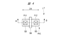
図4は、本実施の形態1の半導体装置の周辺回路領域2Aに形成されるトランジスタを示す平面図である。
FIG. 4 is a plan view showing a transistor formed in the
周辺回路領域2Aには、論理回路を構成するトランジスタとして、複数のnチャネル型MISFETと複数のpチャネル型MISFETとが形成されているが、図4には、論理回路を構成するトランジスタのうちの一つのnチャネル型MISFETを周辺トランジスタLTとして示されている。
In the
図4に示されるように、周辺回路領域2Aには、活性領域AcLが形成され、この活性領域AcLを横切るように周辺トランジスタLTのゲート電極Gltが配置され、ゲート電極Gltの両側であって、活性領域AcLの内部には、後述するn+型半導体領域SDを含む周辺トランジスタLTのソース・ドレイン領域が形成されている。また、周辺トランジスタLTのソース・ドレイン領域上には、プラグPt1、Pt2が配置されている。
As shown in FIG. 4, in the
図4においては、1つの周辺トランジスタLTのみを示しているが、実際には、周辺回路領域2Aには、複数のトランジスタが配置されている。これらの複数のトランジスタのソース・ドレイン領域上のプラグまたはゲート電極Glt上のプラグを複数の配線層(後述の配線M1〜M3)により接続することで、論理回路を構成することができる。また、MISFET以外の素子、例えば、容量素子や他の構成のトランジスタなどが論理回路に組み込まれる場合もある。
Although only one peripheral transistor LT is shown in FIG. 4, a plurality of transistors are actually arranged in the
なお、以下では、周辺トランジスタLTがnチャネル型MISFETである例を説明するが、周辺トランジスタLTはpチャネル型MISFETであってもよい。 Hereinafter, an example in which the peripheral transistor LT is an n-channel MISFET will be described, but the peripheral transistor LT may be a p-channel MISFET.
<画素領域および周辺回路領域の素子構造>
次に、本実施の形態1の半導体装置の断面図(図5および図6)を参照しながら、本実施の形態1の半導体装置の構造を説明する。図5および図6は、本実施の形態1の半導体装置の断面図であり、図5は、図3のA−A線に沿った断面図にほぼ対応し、図6は、図4のB−B線での断面図にほぼ対応している。
<Element structure of pixel area and peripheral circuit area>
Next, the structure of the semiconductor device of the first embodiment will be described with reference to cross-sectional views (FIGS. 5 and 6) of the semiconductor device of the first embodiment. 5 and 6 are cross-sectional views of the semiconductor device according to the first embodiment. FIG. 5 substantially corresponds to the cross-sectional view along the line AA in FIG. 3, and FIG. It almost corresponds to the cross-sectional view taken along the line -B.
図5に示されるように、半導体基板SBの画素領域1Aの活性領域AcTPには、フォトダイオードPDと転送トランジスタTXとが形成されている。フォトダイオードPDは、半導体基板SBに形成されたp型ウエルPW1、n型半導体領域(n型ウエル)NWおよびp型半導体領域PRからなる。また、図6に示されるように、半導体基板SBの周辺回路領域2Aの活性領域AcLには、周辺トランジスタLTが形成されている。
As shown in FIG. 5, a photodiode PD and a transfer transistor TX are formed in the active region AcTP of the pixel region 1A of the semiconductor substrate SB. The photodiode PD includes a p-type well PW1, an n-type semiconductor region (n-type well) NW, and a p-type semiconductor region PR formed in the semiconductor substrate SB. Further, as shown in FIG. 6, a peripheral transistor LT is formed in the active region AcL of the
半導体基板SBは、例えば、リン(P)またはヒ素(As)などのn型不純物(ドナー)が導入されたn型の単結晶シリコンなどからなる半導体基板(半導体ウエハ)である。他の形態として、半導体基板SBを、いわゆるエピタキシャルウエハとすることもできる。半導体基板SBをエピタキシャルウエハとする場合、例えば、n型不純物(例えばヒ素(As))が導入されたn+型の単結晶シリコン基板の主面上に、n型不純物(例えばリン(P))が導入されたn−型単結晶シリコンからなるエピタキシャル層を成長させることにより、半導体基板SBを形成することができる。 The semiconductor substrate SB is a semiconductor substrate (semiconductor wafer) made of n-type single crystal silicon into which an n-type impurity (donor) such as phosphorus (P) or arsenic (As) is introduced. As another form, the semiconductor substrate SB can be a so-called epitaxial wafer. When the semiconductor substrate SB is an epitaxial wafer, for example, an n-type impurity (for example, phosphorus (P)) is formed on the main surface of an n + type single crystal silicon substrate into which an n-type impurity (for example, arsenic (As)) is introduced. The semiconductor substrate SB can be formed by growing an epitaxial layer made of n − type single crystal silicon into which is introduced.
活性領域AcTPの外周には、絶縁体からなる素子分離領域LCSが配置されている。このように、素子分離領域LCSで囲まれた半導体基板SBの露出領域が、活性領域AcTPおよび活性領域AcLなどの活性領域となる。 An element isolation region LCS made of an insulator is arranged on the outer periphery of the active region AcTP. Thus, the exposed region of the semiconductor substrate SB surrounded by the element isolation region LCS becomes an active region such as the active region AcTP and the active region AcL.
半導体基板SBの主面から所定の深さにわたって、p型ウエル(p型半導体領域)PW1,PW2が形成されている。p型ウエルPW1は、活性領域AcTP全体にわたって形成されている。すなわち、p型ウエルPW1は、フォトダイオードPDが形成されている領域と、転送トランジスタTXが形成されている領域とにわたって形成されている。また、p型ウエルPW2は、活性領域AcL全体にわたって形成されている。すなわち、p型ウエルPW2は、周辺トランジスタLTが形成される領域に形成されている。p型ウエルPW1およびp型ウエルPW2は、いずれも、ホウ素(B)などのp型不純物が導入されたp型の半導体領域である。p型ウエルPW1とp型ウエルPW2とは、互いに、独立した領域であり、電気的にも独立である。 P-type wells (p-type semiconductor regions) PW1 and PW2 are formed from the main surface of the semiconductor substrate SB to a predetermined depth. The p-type well PW1 is formed over the entire active region AcTP. That is, the p-type well PW1 is formed across a region where the photodiode PD is formed and a region where the transfer transistor TX is formed. The p-type well PW2 is formed over the entire active region AcL. That is, the p-type well PW2 is formed in a region where the peripheral transistor LT is formed. Each of the p-type well PW1 and the p-type well PW2 is a p-type semiconductor region into which a p-type impurity such as boron (B) is introduced. The p-type well PW1 and the p-type well PW2 are regions independent of each other and are also electrically independent.
図5に示されるように、活性領域AcTPの半導体基板SBにおいて、p型ウエルPW1に内包されるように、n型半導体領域(n型ウエル)NWが形成されている。n型半導体領域NWは、リン(P)またはヒ素(As)などのn型不純物が導入されたn型の半導体領域である。 As shown in FIG. 5, in the semiconductor substrate SB in the active region AcTP, an n-type semiconductor region (n-type well) NW is formed so as to be included in the p-type well PW1. The n-type semiconductor region NW is an n-type semiconductor region into which an n-type impurity such as phosphorus (P) or arsenic (As) is introduced.
n型半導体領域NWは、フォトダイオードPDを形成するためのn型半導体領域であるが、転送トランジスタTXのソース領域でもある。すなわち、n型半導体領域NWは、主として、フォトダイオードPDが形成されている領域に形成されているが、n型半導体領域NWの一部は、転送トランジスタTXのゲート電極Gtと平面的に(平面視で)重なるような位置に、形成されている。n型半導体領域NW(の底面)の深さは、p型ウエルPW1(の底面)の深さよりも浅く形成されている。 The n-type semiconductor region NW is an n-type semiconductor region for forming the photodiode PD, but is also a source region of the transfer transistor TX. That is, the n-type semiconductor region NW is mainly formed in a region where the photodiode PD is formed, but a part of the n-type semiconductor region NW is planarly (planar) with the gate electrode Gt of the transfer transistor TX. It is formed in the position where it overlaps (by visual observation). The depth of the n-type semiconductor region NW (the bottom surface thereof) is formed shallower than the depth of the p-type well PW1 (the bottom surface thereof).
n型半導体領域NWの表面の一部には、p型半導体領域PRが形成されている。p型半導体領域PRは、ホウ素(B)などのp型不純物が高濃度で導入(ドープ)されたp型の半導体領域であり、p型半導体領域PRの不純物濃度(p型不純物濃度)は、p型ウエルPW1の不純物濃度(p型不純物濃度)よりも高い。このため、p型半導体領域PRの導電率(電気伝導率)は、p型ウエルPW1の導電率(電気伝導率)よりも高い。 A p-type semiconductor region PR is formed on a part of the surface of the n-type semiconductor region NW. The p-type semiconductor region PR is a p-type semiconductor region into which p-type impurities such as boron (B) are introduced (doped) at a high concentration. The impurity concentration (p-type impurity concentration) of the p-type semiconductor region PR is It is higher than the impurity concentration (p-type impurity concentration) of the p-type well PW1. For this reason, the conductivity (electric conductivity) of the p-type semiconductor region PR is higher than the conductivity (electric conductivity) of the p-type well PW1.
p型半導体領域PR(の底面)の深さは、n型半導体領域NW(の底面)の深さよりも浅い。p型半導体領域PRは、主として、n型半導体領域NWの表層部分(表面部分)に形成される。このため、半導体基板SBの厚さ方向に見ると、最上層のp型半導体領域PRの下にn型半導体領域NWが存在し、n型半導体領域NWの下にp型ウエルPW1が存在する状態となる。 The depth of the p-type semiconductor region PR (the bottom surface thereof) is shallower than the depth of the n-type semiconductor region NW (the bottom surface thereof). The p-type semiconductor region PR is mainly formed in the surface layer portion (surface portion) of the n-type semiconductor region NW. Therefore, when viewed in the thickness direction of the semiconductor substrate SB, the n-type semiconductor region NW exists below the uppermost p-type semiconductor region PR, and the p-type well PW1 exists below the n-type semiconductor region NW. It becomes.
また、n型半導体領域NWが形成されていない領域において、p型半導体領域PRの一部はp型ウエルPW1に接している。すなわち、p型半導体領域PRは、直下にn型半導体領域NWが存在してそのn型半導体領域NWに接する部分と、直下にp型ウエルPW1が存在してそのp型ウエルPW1に接する部分とを有している。 In the region where the n-type semiconductor region NW is not formed, a part of the p-type semiconductor region PR is in contact with the p-type well PW1. That is, the p-type semiconductor region PR includes a portion where the n-type semiconductor region NW exists immediately below and contacts the n-type semiconductor region NW, and a portion where the p-type well PW1 exists immediately below and contacts the p-type well PW1. have.
p型ウエルPW1とn型半導体領域NWとの間には、PN接合が形成される。また、p型半導体領域PRとn型半導体領域NWとの間には、PN接合が形成される。p型ウエルPW1(p型半導体領域)とn型半導体領域NWとp型半導体領域PRとによって、フォトダイオード(PN接合ダイオード)PDが形成される。フォトダイオードPDは、受光素子であり、光電変換素子である。フォトダイオードPDは、入力された光を光電変換して電荷を生成し、生成した電荷を蓄積する機能を有する。n型半導体領域NWには、フォトダイオードPDで光電変換された電荷が蓄積されるので、n型半導体領域NWはフォトダイオードPDの電荷蓄積層と呼ぶことができる。また、p型半導体領域PRは、半導体基板SBの主面側に形成されていることから、表面層と呼ぶことができる。 A PN junction is formed between the p-type well PW1 and the n-type semiconductor region NW. A PN junction is formed between the p-type semiconductor region PR and the n-type semiconductor region NW. A photodiode (PN junction diode) PD is formed by the p-type well PW1 (p-type semiconductor region), the n-type semiconductor region NW, and the p-type semiconductor region PR. The photodiode PD is a light receiving element and a photoelectric conversion element. The photodiode PD has a function of photoelectrically converting input light to generate charges and storing the generated charges. Since the charge photoelectrically converted by the photodiode PD is stored in the n-type semiconductor region NW, the n-type semiconductor region NW can be called a charge storage layer of the photodiode PD. Further, since the p-type semiconductor region PR is formed on the main surface side of the semiconductor substrate SB, it can be called a surface layer.
表面層(p型半導体領域PR)は、半導体基板SBの表面に多数形成されている界面準位に基づく電子の発生を抑制する目的で形成されている。すなわち、半導体基板SBの表面領域では、界面準位の影響により、光が照射されていない状態でも電子が発生し、暗電流の増加を引き起こす場合がある。このため、電子を多数キャリアとするn型半導体領域NWの表面に、正孔(ホール)を多数キャリアとするp型半導体領域PRである表面層を形成することにより、光が照射されていない状態での電子の発生を抑制し、暗電流の増加を抑制することができる。従って、表面層は、フォトダイオード最表面から湧き出る電子をそのp型半導体領域のホールと再結合させて、暗電流または暗時白欠陥を減少させる役割がある。 The surface layer (p-type semiconductor region PR) is formed for the purpose of suppressing the generation of electrons based on interface states formed in large numbers on the surface of the semiconductor substrate SB. That is, in the surface region of the semiconductor substrate SB, electrons are generated due to the influence of the interface state, which may cause an increase in dark current even when light is not irradiated. For this reason, a surface layer that is a p-type semiconductor region PR having holes as majority carriers is formed on the surface of the n-type semiconductor region NW having electrons as majority carriers, so that no light is irradiated. The generation of electrons at can be suppressed, and an increase in dark current can be suppressed. Therefore, the surface layer has a role of reducing dark current or dark white defects by recombining electrons springing from the outermost surface of the photodiode with holes in the p-type semiconductor region.
本実施の形態1の半導体装置では、表面層は、p型半導体領域であるサブ領域PR1とp型半導体領域であるサブ領域PR2とで構成されている。サブ領域PR2の不純物濃度は、サブ領域PR1の不純物濃度よりも高い。半導体基板SBの深さ方向において、サブ領域PR1の底面は、サブ領域PR2の底面よりも深い位置に形成されており、サブ領域PR1がn型半導体領域である電荷蓄積層(n型半導体領域NW)と接している。また、半導体基板SBの主面に沿う方向において、サブ領域PR1は、サブ領域PR2よりも、後述するゲート電極GtまたはフローティングディフュージョンFDに近い側に配置されている。 In the semiconductor device of the first embodiment, the surface layer is composed of a sub-region PR1 that is a p-type semiconductor region and a sub-region PR2 that is a p-type semiconductor region. The impurity concentration of the sub region PR2 is higher than the impurity concentration of the sub region PR1. In the depth direction of the semiconductor substrate SB, the bottom surface of the sub-region PR1 is formed at a position deeper than the bottom surface of the sub-region PR2, and the charge accumulation layer (n-type semiconductor region NW) in which the sub-region PR1 is an n-type semiconductor region. ). Further, in the direction along the main surface of the semiconductor substrate SB, the sub-region PR1 is disposed closer to a gate electrode Gt (described later) or the floating diffusion FD than the sub-region PR2.
転送トランジスタTXは、フォトダイオードPDで発生し、蓄積された電荷をフォトダイオードPDから転送する際のスイッチとしての役割を有している。 The transfer transistor TX has a role as a switch when transferring the accumulated electric charge generated and accumulated in the photodiode PD from the photodiode PD.
また、n型半導体領域NWの一部と平面的に重なるように、ゲート電極Gtが形成されている。このゲート電極Gtは、転送トランジスタTXのゲート電極であり、半導体基板SB上にゲート絶縁膜GOXを介して形成(配置)されている。転送トランジスタTXのフローティングディフュージョンFD側には、ゲート電極Gtの側壁上に、オフセットスペーサOSを介して、側壁絶縁膜としてサイドウォールスペーサSWが形成されている。 Further, the gate electrode Gt is formed so as to overlap with a part of the n-type semiconductor region NW in a plan view. The gate electrode Gt is a gate electrode of the transfer transistor TX, and is formed (arranged) on the semiconductor substrate SB via the gate insulating film GOX. On the floating diffusion FD side of the transfer transistor TX, a sidewall spacer SW is formed as a sidewall insulating film on the sidewall of the gate electrode Gt via an offset spacer OS.
活性領域AcTPの半導体基板SB(p型ウエルPW1)において、ゲート電極Gtの両側のうちの一方の側には、n型半導体領域NWが形成されており、他方の側には、n型半導体領域NRが形成されている。n型半導体領域NRは、リン(P)またはヒ素(As)などのn型不純物が高濃度で導入(ドープ)されたn+型半導体領域であり、p型ウエルPW1内に形成されている。n型半導体領域NRは、フローティングディフュージョン(浮遊拡散層)FDとしての半導体領域であり、転送トランジスタTXのドレイン領域でもある。 In the semiconductor substrate SB (p-type well PW1) of the active region AcTP, an n-type semiconductor region NW is formed on one side of both sides of the gate electrode Gt, and an n-type semiconductor region is formed on the other side. NR is formed. The n-type semiconductor region NR is an n + -type semiconductor region into which n-type impurities such as phosphorus (P) or arsenic (As) are introduced (doped) at a high concentration, and is formed in the p-type well PW1. The n-type semiconductor region NR is a semiconductor region as a floating diffusion (floating diffusion layer) FD, and is also a drain region of the transfer transistor TX.
n型半導体領域NWは、フォトダイオードPDの電荷蓄積層であり、転送トランジスタTXのソース用の半導体領域としても機能することができる。すなわち、転送トランジスタTXのソース領域は、n型半導体領域NWにより形成される。このため、n型半導体領域NWとゲート電極Gtとは、ゲート電極Gtの一部(ソース側)が、n型半導体領域NWの一部と平面的に(平面視で)重なるような位置関係となっている。n型半導体領域NWとn型半導体領域NRとは、転送トランジスタTXのチャネル形成領域(ゲート電極Gtの直下の基板領域に対応)を挟んで互いに離間するように形成されている。 The n-type semiconductor region NW is a charge storage layer of the photodiode PD, and can also function as a semiconductor region for the source of the transfer transistor TX. That is, the source region of the transfer transistor TX is formed by the n-type semiconductor region NW. For this reason, the n-type semiconductor region NW and the gate electrode Gt have a positional relationship such that a part (source side) of the gate electrode Gt overlaps a part of the n-type semiconductor region NW in plan view. It has become. The n-type semiconductor region NW and the n-type semiconductor region NR are formed so as to be separated from each other with a channel formation region (corresponding to a substrate region immediately below the gate electrode Gt) of the transfer transistor TX interposed therebetween.
フォトダイオードPD(図5参照)の表面、すなわち表面層上には、例えば、窒化シリコン膜や酸化シリコン膜からなるオフセットスペーサOSが形成されている。このオフセットスペーサOSは、半導体基板SBの表面特性、すなわち界面特性を良好に保つために形成される。このオフセットスペーサOS上には、酸化シリコン膜からなる反射防止膜ARFが形成されている。すなわち、反射防止膜ARFは、n型半導体領域NWおよび表面層の上に、オフセットスペーサOSを介して形成されている。反射防止膜ARFおよびオフセットスペーサOSの一部(端部)は、ゲート電極Gt上に乗り上げている。 An offset spacer OS made of, for example, a silicon nitride film or a silicon oxide film is formed on the surface of the photodiode PD (see FIG. 5), that is, on the surface layer. The offset spacer OS is formed in order to keep the surface characteristics of the semiconductor substrate SB, that is, the interface characteristics. On the offset spacer OS, an antireflection film ARF made of a silicon oxide film is formed. That is, the antireflection film ARF is formed on the n-type semiconductor region NW and the surface layer via the offset spacer OS. A part (end) of the antireflection film ARF and the offset spacer OS rides on the gate electrode Gt.
一方、図6に示されるように、活性領域AcLのp型ウエルPW2上には、ゲート絶縁膜GOXを介して、周辺トランジスタLTのゲート電極Gltが形成されており、ゲート電極Gltの両側の側壁上には、オフセットスペーサOSを介してサイドウォールスペーサSWが形成されている。また、ゲート電極Gltの両側のp型ウエルPW2中には、周辺トランジスタLTのソース・ドレイン領域が形成されている。周辺トランジスタLTのソース・ドレイン領域は、LDD(Lightly Doped Drain)構造を有しており、n型の低濃度半導体領域であるn−型半導体領域NMと、n型の高濃度半導体領域であるn+型半導体領域SDとからなる。さらに、周辺トランジスタLTのゲート電極Glt、ソース・ドレイン領域を構成するn+型半導体領域SDの表面には金属シリサイド層を形成してもよい。 On the other hand, as shown in FIG. 6, the gate electrode Glt of the peripheral transistor LT is formed on the p-type well PW2 in the active region AcL via the gate insulating film GOX, and the side walls on both sides of the gate electrode Glt. A sidewall spacer SW is formed on the top via an offset spacer OS. In the p-type well PW2 on both sides of the gate electrode Glt, source / drain regions of the peripheral transistor LT are formed. The source / drain regions of the peripheral transistor LT have an LDD (Lightly Doped Drain) structure, and an n − type semiconductor region NM that is an n-type low concentration semiconductor region and an n type high concentration semiconductor region. It comprises a + type semiconductor region SD. Furthermore, a metal silicide layer may be formed on the surface of the gate electrode Glt of the peripheral transistor LT and the n + type semiconductor region SD constituting the source / drain regions.
図5および図6に示されるように、半導体基板SB上には、ゲート電極Gt、反射防止膜ARFおよびゲート電極Gltを覆うように、層間絶縁膜IL1が形成されている。層間絶縁膜IL1は、画素領域1Aおよび周辺回路領域2Aを含む半導体基板SBの主面全体上に形成されている。層間絶縁膜IL1は、例えば、TEOS(Tetra Ethyl Ortho Silicate)を原料とした酸化シリコン膜により形成されている。層間絶縁膜IL1には、プラグPfd,Ptg,Pt1,Pt2などの導電性のプラグPGが埋め込まれている。例えば、図5に示されるように、フローティングディフュージョンFDとしてのn型半導体領域NR上にプラグPGとしてプラグPfdが形成されており、このプラグPfdは、層間絶縁膜IL1を貫通してn型半導体領域NRに達しており、n型半導体領域NRと電気的に接続されている。
As shown in FIGS. 5 and 6, an interlayer insulating film IL1 is formed on the semiconductor substrate SB so as to cover the gate electrode Gt, the antireflection film ARF, and the gate electrode Glt. The interlayer insulating film IL1 is formed over the entire main surface of the semiconductor substrate SB including the pixel region 1A and the
プラグPfd,Ptg,Pt1,Pt2などの導電性のプラグPGは、層間絶縁膜IL1に形成されたコンタクトホールに、例えば、バリア導体膜とバリア導体膜上に形成されたタングステン膜とを埋め込むことにより形成されている。そのバリア導体膜は、例えば、チタン膜と該チタン膜上に形成された窒化チタン膜との積層膜(すなわちチタン/窒化チタン膜)からなる。 Conductive plugs PG such as plugs Pfd, Ptg, Pt1, and Pt2 are formed by embedding, for example, a barrier conductor film and a tungsten film formed on the barrier conductor film in a contact hole formed in the interlayer insulating film IL1. Is formed. The barrier conductor film is made of, for example, a laminated film of a titanium film and a titanium nitride film formed on the titanium film (that is, a titanium / titanium nitride film).
プラグPG(Pfd,Ptg,Pt1,Pt2)が埋め込まれた層間絶縁膜IL1上には、例えば、層間絶縁膜IL2が形成されており、この層間絶縁膜IL2に配線M1が形成されている。 For example, an interlayer insulating film IL2 is formed on the interlayer insulating film IL1 in which the plugs PG (Pfd, Ptg, Pt1, Pt2) are embedded, and a wiring M1 is formed in the interlayer insulating film IL2.
層間絶縁膜IL2は、例えば酸化シリコン膜により形成されるが、これに限定されるものではなく、酸化シリコン膜よりも誘電率の低い低誘電率膜により形成することもできる。低誘電率膜としては、例えば、SiOC膜を挙げることができる。 The interlayer insulating film IL2 is formed of, for example, a silicon oxide film, but is not limited to this, and may be formed of a low dielectric constant film having a dielectric constant lower than that of the silicon oxide film. An example of the low dielectric constant film is a SiOC film.
配線M1は、例えば、銅配線により形成されており、ダマシン法を用いて形成することができる。なお、配線M1は、銅配線に限定されるものではなく、アルミニウム配線により形成することもできる。配線M1が埋込銅配線(ダマシン銅配線)の場合(図5および図6はこの場合に対応)は、その埋込銅配線は、層間絶縁膜IL1に形成された配線溝内に埋め込まれているが、配線M1がアルミニウム配線の場合は、そのアルミニウム配線は、層間絶縁膜上に形成された導電膜をパターニングすることにより形成される。 The wiring M1 is formed of, for example, a copper wiring, and can be formed using a damascene method. Note that the wiring M1 is not limited to a copper wiring, and can be formed of an aluminum wiring. When the wiring M1 is a buried copper wiring (damascene copper wiring) (FIGS. 5 and 6 correspond to this case), the buried copper wiring is buried in a wiring trench formed in the interlayer insulating film IL1. However, when the wiring M1 is an aluminum wiring, the aluminum wiring is formed by patterning a conductive film formed on the interlayer insulating film.
配線M1を形成した層間絶縁膜IL2上には、例えば、酸化シリコン膜や低誘電率膜からなる層間絶縁膜IL3が形成されており、この層間絶縁膜IL3に配線M2が形成されている。また、配線M2を形成した層間絶縁膜IL3上には、層間絶縁膜IL4が形成されており、この層間絶縁膜IL4に配線M3が形成されている。配線M1〜M3は、配線層を形成している。配線M1〜M3は、フォトダイオードと平面的に重ならないように形成されている。これは、フォトダイオードに入射する光が配線M1〜M3によって遮られないようにするためである。 On the interlayer insulating film IL2 on which the wiring M1 is formed, for example, an interlayer insulating film IL3 made of a silicon oxide film or a low dielectric constant film is formed, and the wiring M2 is formed in the interlayer insulating film IL3. An interlayer insulating film IL4 is formed on the interlayer insulating film IL3 on which the wiring M2 is formed, and the wiring M3 is formed in the interlayer insulating film IL4. The wirings M1 to M3 form a wiring layer. The wirings M1 to M3 are formed so as not to overlap the photodiode in plan view. This is to prevent light incident on the photodiode from being blocked by the wirings M1 to M3.
さらに、配線M3を形成した層間絶縁膜IL4上には、マイクロレンズMLが搭載されている。なお、マイクロレンズMLと層間絶縁膜IL4との間にカラーフィルタが設けられていてもよい。 Further, a microlens ML is mounted on the interlayer insulating film IL4 on which the wiring M3 is formed. A color filter may be provided between the microlens ML and the interlayer insulating film IL4.
図5において、光が画素PU(図1参照)に照射されると、まず、入射光は、マイクロレンズMLを通過する。その後、可視光に対して透明な層間絶縁膜IL4〜IL1を通過した後、反射防止膜ARFに入射する。反射防止膜ARFでは、入射光の反射が抑制されて充分な光量の入射光がフォトダイオードPDに入射する。フォトダイオードPDでは、入射光のエネルギーがシリコンのバンドギャップよりも大きいため、光電変換により入射光が吸収されて正孔電子対が生成される。このとき生成された電子は、n型半導体領域NWに蓄積される。そして、適切なタイミングで、転送トランジスタTXをオンする。具体的には、転送トランジスタTXのゲート電極Gtにしきい値電圧以上の電圧を印加する。すると、転送トランジスタTXのゲート絶縁膜GOX直下のチャネル形成領域にチャネル領域が形成され、転送トランジスタTXのソース領域としてのn型半導体領域NWと、転送トランジスタTXのドレイン領域としてのn型半導体領域NRとが、電気的に導通することになる。この結果、n型半導体領域NWに蓄積された電子は、チャネル領域を通ってドレイン領域(n型半導体領域NR)に達し、ドレイン領域(n型半導体領域NR)からプラグPfdおよび配線層を伝わって外部回路に取り出される。 In FIG. 5, when light is irradiated onto the pixel PU (see FIG. 1), first, the incident light passes through the microlens ML. Thereafter, the light passes through the interlayer insulating films IL4 to IL1 transparent to visible light, and then enters the antireflection film ARF. In the antireflection film ARF, reflection of incident light is suppressed, and a sufficient amount of incident light is incident on the photodiode PD. In the photodiode PD, since the energy of incident light is larger than the band gap of silicon, the incident light is absorbed by photoelectric conversion and a hole electron pair is generated. The electrons generated at this time are accumulated in the n-type semiconductor region NW. Then, the transfer transistor TX is turned on at an appropriate timing. Specifically, a voltage equal to or higher than the threshold voltage is applied to the gate electrode Gt of the transfer transistor TX. Then, a channel region is formed in the channel formation region immediately below the gate insulating film GOX of the transfer transistor TX, and the n-type semiconductor region NW as the source region of the transfer transistor TX and the n-type semiconductor region NR as the drain region of the transfer transistor TX. Is electrically conducted. As a result, electrons accumulated in the n-type semiconductor region NW pass through the channel region to reach the drain region (n-type semiconductor region NR), and are transmitted from the drain region (n-type semiconductor region NR) to the plug Pfd and the wiring layer. Taken out to an external circuit.
<半導体装置の製造方法>
次に、本実施の形態1の半導体装置の製造方法について、図5〜図24を参照して説明する。図面簡略化のために図23および図24に続く製造工程は、図5および図6を用いて説明する。
<Method for Manufacturing Semiconductor Device>
Next, a method for manufacturing the semiconductor device according to the first embodiment will be described with reference to FIGS. For simplification of the drawing, the manufacturing process subsequent to FIGS. 23 and 24 will be described with reference to FIGS.
図7および図8は、本実施の形態1の半導体装置の製造工程を示す工程フロー図である。図9〜図24ならびに図5および図6は、本実施の形態1の半導体装置の製造工程中の要部断面図である。図9〜図24のうち、図9、図11、図13、図15、図17、図19、図21および図23は、図5に相当する断面図、すなわち、図3のA−A線に沿う位置での断面図である。図7〜図24のうち、図10、図12、図14、図16、図18、図20、図22および図24は、図6に相当する断面図、すなわち、図4のB−B線に沿う位置での断面図である。 7 and 8 are process flowcharts showing the manufacturing process of the semiconductor device of the first embodiment. 9 to 24 and FIGS. 5 and 6 are main-portion cross-sectional views during the manufacturing process of the semiconductor device of the first embodiment. 9 to 24, FIGS. 9, 11, 13, 15, 17, 19, 21, and 23 are cross-sectional views corresponding to FIG. 5, that is, the line AA in FIG. 3. It is sectional drawing in the position in alignment with. 7 to 24, FIGS. 10, 12, 14, 16, 18, 20, 22, and 24 are cross-sectional views corresponding to FIG. 6, that is, the line BB in FIG. 4. It is sectional drawing in the position in alignment with.
本実施の形態1の半導体装置を製造するために、まず、図7のS1工程に示されるように、半導体基板(半導体ウエハ)SBを用意(準備)する。 In order to manufacture the semiconductor device of the first embodiment, first, a semiconductor substrate (semiconductor wafer) SB is prepared (prepared) as shown in step S1 of FIG.
半導体基板SBは、例えば、リン(P)またはヒ素(As)などのn型不純物が導入されたn型の単結晶シリコンなどからなる半導体基板(半導体ウエハ)である。他の形態として、半導体基板SBを、いわゆるエピタキシャルウエハとすることもできる。半導体基板SBをエピタキシャルウエハとする場合、例えば、n型不純物(例えばヒ素(As))が導入されたn+型の単結晶シリコン基板の主面上に、n型不純物(例えばリン(P))が導入されたn−型単結晶シリコンからなるエピタキシャル層を成長させることにより、半導体基板SBを形成することができる。 The semiconductor substrate SB is a semiconductor substrate (semiconductor wafer) made of n-type single crystal silicon into which an n-type impurity such as phosphorus (P) or arsenic (As) is introduced, for example. As another form, the semiconductor substrate SB can be a so-called epitaxial wafer. When the semiconductor substrate SB is an epitaxial wafer, for example, an n-type impurity (for example, phosphorus (P)) is formed on the main surface of an n + type single crystal silicon substrate into which an n-type impurity (for example, arsenic (As)) is introduced. The semiconductor substrate SB can be formed by growing an epitaxial layer made of n − type single crystal silicon into which is introduced.
次に、図9および図10は、半導体基板SBに素子分離領域LCSを形成する工程(図7のS2工程)を示している。 Next, FIG. 9 and FIG. 10 show a step of forming the element isolation region LCS in the semiconductor substrate SB (step S2 in FIG. 7).
素子分離領域LCSは、酸化膜などの絶縁膜からなる。例えば、半導体基板SBのうち、活性領域AcTPおよび活性領域AcL等の活性領域となる領域を窒化シリコン膜で覆った状態で、半導体基板SBを熱酸化することにより、窒化シリコン膜で覆われていない領域の半導体基板SBの主面に、熱酸化膜からなる素子分離領域LCSを形成することができる。このような素子分離領域の形成法をLOCOS(Local oxidation of silicon)法という。素子分離領域LCSにより、活性領域AcTPおよび活性領域AcL等の活性領域が区画(規定)される。 The element isolation region LCS is made of an insulating film such as an oxide film. For example, the semiconductor substrate SB is not covered with the silicon nitride film by thermally oxidizing the semiconductor substrate SB in a state where the active regions such as the active region AcTP and the active region AcL are covered with the silicon nitride film. An element isolation region LCS made of a thermal oxide film can be formed on the main surface of the semiconductor substrate SB in the region. Such a method for forming an element isolation region is called a LOCOS (Local oxidation of silicon) method. The active regions such as the active region AcTP and the active region AcL are partitioned (defined) by the element isolation region LCS.
LOCOS法に代えてSTI(Shallow Trench Isolation)法を用いて素子分離領域LCSを形成してもよい。STI法を用いた場合、素子分離領域LCSは、半導体基板SBの溝内に埋め込まれた絶縁膜(例えば酸化シリコン膜)からなる。例えば、半導体基板SBのうち、活性領域AcTPおよび活性領域AcL等の活性領域となる領域を窒化シリコン膜で覆う。そして、その窒化シリコン膜をエッチングマスクとして半導体基板SBをエッチングすることにより、半導体基板SBに素子分離用の溝を形成し、その後、その素子分離用の溝内に酸化シリコン膜などの絶縁膜を埋め込むことにより、素子分離領域LCSを形成することができる。 The element isolation region LCS may be formed using an STI (Shallow Trench Isolation) method instead of the LOCOS method. When the STI method is used, the element isolation region LCS is made of an insulating film (for example, a silicon oxide film) embedded in the trench of the semiconductor substrate SB. For example, in the semiconductor substrate SB, regions that become active regions such as the active region AcTP and the active region AcL are covered with a silicon nitride film. Then, by etching the semiconductor substrate SB using the silicon nitride film as an etching mask, an element isolation groove is formed in the semiconductor substrate SB, and then an insulating film such as a silicon oxide film is formed in the element isolation groove. By embedding, the element isolation region LCS can be formed.
なお、活性領域AcTPは、画素領域1Aに形成され、活性領域AcLは、周辺回路領域2Aに形成される。
The active region AcTP is formed in the pixel region 1A, and the active region AcL is formed in the
次に、図11および図12は、画素領域1Aの半導体基板SBにp型ウエル(p型半導体領域)PW1を形成する工程、周辺回路領域2Aの半導体基板SBにp型ウエル(p型半導体領域)PW2を形成する工程(図7のS3工程)を示している。 Next, FIGS. 11 and 12 show a step of forming a p-type well (p-type semiconductor region) PW1 in the semiconductor substrate SB in the pixel region 1A, and a p-type well (p-type semiconductor region) in the semiconductor substrate SB in the peripheral circuit region 2A. ) A step of forming PW2 (step S3 in FIG. 7).
p型ウエルPW1は、フォトダイオードPDを形成するためのp型半導体領域であり、また、nチャネル型の転送トランジスタTXを形成するためのp型ウエル領域でもある。p型ウエルPW2は、nチャネル型の周辺トランジスタLTを形成するためのp型ウエル領域である。 The p-type well PW1 is a p-type semiconductor region for forming the photodiode PD, and is also a p-type well region for forming the n-channel type transfer transistor TX. The p-type well PW2 is a p-type well region for forming the n-channel peripheral transistor LT.
p型ウエルPW1,PW2は、それぞれ、半導体基板SBの主面から所定の深さにわたって形成される。p型ウエルPW1,PW2は、半導体基板SBに、例えばホウ素(B)などのp型の不純物をイオン注入することなどによって形成することができる。 The p-type wells PW1 and PW2 are each formed over a predetermined depth from the main surface of the semiconductor substrate SB. The p-type wells PW1 and PW2 can be formed by ion-implanting a p-type impurity such as boron (B) into the semiconductor substrate SB.
p型ウエルPW1は、画素領域1Aにおいて、フォトダイオードPDが形成される領域と、転送トランジスタTXが形成される領域とにわたって形成される。すなわち、画素領域1Aにおいて、活性領域AcTP全体にp型ウエルPW1が形成される。p型ウエルPW2は、周辺回路領域2Aに形成される。p型ウエルPW1を形成するためのイオン注入と、p型ウエルPW2を形成するためのイオン注入とは、異なるイオン注入工程で行うか、あるいは、同じイオン注入工程で行う。
The p-type well PW1 is formed in the pixel region 1A over a region where the photodiode PD is formed and a region where the transfer transistor TX is formed. That is, in the pixel region 1A, the p-type well PW1 is formed in the entire active region AcTP. The p-type well PW2 is formed in the
p型ウエルPW1,PW2の導電型はp型であり、半導体基板SBの導電型であるn型とは反対の導電型である。p型ウエルPW1,PW2は、半導体基板SBの主面を基準として、素子分離領域LCSよりも深い。 The conductivity type of the p-type wells PW1 and PW2 is p-type, and is the conductivity type opposite to the n-type which is the conductivity type of the semiconductor substrate SB. The p-type wells PW1 and PW2 are deeper than the element isolation region LCS with respect to the main surface of the semiconductor substrate SB.
次に、図13および図14は、ゲート電極Gt、Gltの形成工程(図7のS4工程)を示している。画素領域1Aにおいて、半導体基板SB(p型ウエルPW1)上にゲート絶縁膜GOXを介して転送トランジスタTX用のゲート電極Gtを形成し、周辺回路領域2Aにおいて、半導体基板SB(p型ウエルPW2)上にゲート絶縁膜GOXを介して周辺トランジスタLT用のゲート電極Gltを形成する。
Next, FIGS. 13 and 14 show a step of forming the gate electrodes Gt and Glt (step S4 in FIG. 7). In the pixel region 1A, the gate electrode Gt for the transfer transistor TX is formed on the semiconductor substrate SB (p-type well PW1) via the gate insulating film GOX. In the
すなわち、まず、半導体基板SBの主面を洗浄処理などにより清浄化してから、半導体基板SBの主面にゲート絶縁膜GOX用の絶縁膜を形成する。このゲート絶縁膜GOX用の絶縁膜は、例えば酸化シリコン膜からなり、熱酸化法などを用いて形成することができる。他の形態として、ゲート絶縁膜GOX用の絶縁膜として、酸窒化シリコン膜や、あるいは、金属酸化物膜(例えばハフニウム酸化物膜)などの高誘電率絶縁膜を用いることもできる。それから、半導体基板SB上、すなわちゲート絶縁膜GOX用の絶縁膜上に、ゲート電極用の導電膜(例えば多結晶シリコン膜)をCVD(Chemical Vapor Deposition)法などを用いて形成した後、このゲート電極用の導電膜をフォトリソグラフィ法およびドライエッチング法を用いてパターニングする。これにより、パターニングされた導電膜(例えば多結晶シリコン膜)からなるゲート電極Gt,Gltを形成することができる。ゲート電極Gt,Gltの下に残存するゲート絶縁膜GOX用の絶縁膜が、ゲート絶縁膜GOXとなる。また、本実施の形態では、このゲート電極用の導電膜をパターニングするためのドライエッチング、あるいはそのドライエッチングの後のウェットエッチングにより、ゲート電極Gt,Gltで覆われていない領域のゲート絶縁膜GOX用の絶縁膜は除去される場合を例示している。しかしながら、ゲート電極Gt,Gltで覆われていない領域の絶縁膜GOXを除去せずに、後の工程で行われるイオン注入の際に保護膜として用いるために残しても良い。 That is, first, the main surface of the semiconductor substrate SB is cleaned by a cleaning process or the like, and then an insulating film for the gate insulating film GOX is formed on the main surface of the semiconductor substrate SB. The insulating film for the gate insulating film GOX is made of, for example, a silicon oxide film, and can be formed using a thermal oxidation method or the like. As another form, a high dielectric constant insulating film such as a silicon oxynitride film or a metal oxide film (for example, a hafnium oxide film) can be used as the insulating film for the gate insulating film GOX. Then, a conductive film (for example, a polycrystalline silicon film) for a gate electrode is formed on the semiconductor substrate SB, that is, the insulating film for the gate insulating film GOX by using a CVD (Chemical Vapor Deposition) method or the like. The electrode conductive film is patterned using a photolithography method and a dry etching method. Thereby, gate electrodes Gt and Glt made of a patterned conductive film (for example, a polycrystalline silicon film) can be formed. The insulating film for the gate insulating film GOX remaining under the gate electrodes Gt and Glt becomes the gate insulating film GOX. In this embodiment, the gate insulating film GOX in a region not covered with the gate electrodes Gt and Glt is formed by dry etching for patterning the conductive film for the gate electrode or wet etching after the dry etching. The case where the insulating film is removed is illustrated. However, the insulating film GOX in the region not covered with the gate electrodes Gt and Glt may be left without being removed for use as a protective film in ion implantation performed in a later process.
ゲート電極Gtは、転送トランジスタTXのゲート電極として機能し、画素領域1Aにおいて、半導体基板SB(p型ウエルPW1)上にゲート絶縁膜GOXを介して形成される。ゲート電極Gtの下のゲート絶縁膜GOXが、転送トランジスタTXのゲート絶縁膜として機能する。ゲート電極Gltは、周辺トランジスタLTのゲート電極として機能し、周辺回路領域2Aにおいて、半導体基板SB(p型ウエルPW2)上にゲート絶縁膜GOXを介して形成される。ゲート電極Gltの下のゲート絶縁膜GOXが、周辺トランジスタLTのゲート絶縁膜として機能する。
The gate electrode Gt functions as a gate electrode of the transfer transistor TX, and is formed on the semiconductor substrate SB (p-type well PW1) via the gate insulating film GOX in the pixel region 1A. The gate insulating film GOX below the gate electrode Gt functions as the gate insulating film of the transfer transistor TX. The gate electrode Glt functions as a gate electrode of the peripheral transistor LT, and is formed on the semiconductor substrate SB (p-type well PW2) via the gate insulating film GOX in the
次に、図15および図16は、n型半導体領域NWの形成工程(図7のS5工程)を示している。画素領域1Aの半導体基板SBに、n型半導体領域NWを形成する。n型半導体領域NWは、画素領域1Aの半導体基板SBにリン(P)またヒ素(As)などのn型の不純物をイオン注入することによって、形成することができる。 Next, FIGS. 15 and 16 show a step of forming the n-type semiconductor region NW (step S5 in FIG. 7). An n-type semiconductor region NW is formed on the semiconductor substrate SB in the pixel region 1A. The n-type semiconductor region NW can be formed by ion-implanting n-type impurities such as phosphorus (P) or arsenic (As) into the semiconductor substrate SB in the pixel region 1A.
n型半導体領域NWは、フォトダイオードPDを形成するためのn型半導体領域であり、n型半導体領域NW(の底面)の深さは、p型ウエルPW1(の底面)の深さよりも浅く、n型半導体領域NWは、p型ウエルPW1に内包されるように形成される。n型半導体領域NWは、p型ウエルPW1に内包されるように形成されるため、n型半導体領域NWの底面と側面とは、p型ウエルPW1に接している。 The n-type semiconductor region NW is an n-type semiconductor region for forming the photodiode PD, and the depth of the n-type semiconductor region NW (the bottom surface) is shallower than the depth of the p-type well PW1 (the bottom surface). The n-type semiconductor region NW is formed so as to be enclosed in the p-type well PW1. Since the n-type semiconductor region NW is formed so as to be included in the p-type well PW1, the bottom surface and the side surface of the n-type semiconductor region NW are in contact with the p-type well PW1.
n型半導体領域NWは、画素領域1Aの活性領域AcTP全体に形成されるのではなく、活性領域AcTPの半導体基板SBにおけるゲート電極Gtの両側の領域のうち、一方の側(ソース側)に形成され、他方側(ドレイン側)には形成されない。 The n-type semiconductor region NW is not formed in the entire active region AcTP of the pixel region 1A, but is formed on one side (source side) of the regions on both sides of the gate electrode Gt in the semiconductor substrate SB of the active region AcTP. However, it is not formed on the other side (drain side).
n型半導体領域NWは、具体的には、例えば次のようにして形成することができる。すなわち、図15および図16に示されるように、まず、半導体基板SB上にレジスト層としてフォトレジストパターン(フォトレジスト層)RS1を、フォトリソグラフィ技術を用いて形成する。フォトレジストパターンRS1は、画素領域1Aの活性領域AcTPにおけるゲート電極Gtの両側のうちの一方の側(ソース側)を開口(露出)する開口部OP1を有しており、画素領域1Aの活性領域AcTPにおけるゲート電極Gtの両側のうちの他方の側(ドレイン側)は、フォトレジストパターンRS1で覆われている。それから、このフォトレジストパターンRS1をマスク(イオン注入阻止マスク)として用いて、半導体基板SBにn型の不純物イオンをイオン注入する。これにより、画素領域1Aにおいて、開口部OP1に平面視で重なる位置の半導体基板SBにn型不純物がイオン注入され、それによって、画素領域1Aの活性領域AcTPの半導体基板SBに、p型ウエルPW1に内包されるように、n型半導体領域NWが形成される。その後、フォトレジストパターンRS1は除去される。 Specifically, the n-type semiconductor region NW can be formed as follows, for example. That is, as shown in FIGS. 15 and 16, first, a photoresist pattern (photoresist layer) RS1 is formed as a resist layer on the semiconductor substrate SB by using a photolithography technique. The photoresist pattern RS1 has an opening OP1 that opens (exposes) one side (source side) of both sides of the gate electrode Gt in the active region AcTP of the pixel region 1A, and the active region of the pixel region 1A. The other side (drain side) of both sides of the gate electrode Gt in AcTP is covered with a photoresist pattern RS1. Then, n-type impurity ions are ion-implanted into the semiconductor substrate SB using the photoresist pattern RS1 as a mask (ion implantation blocking mask). Thereby, in the pixel region 1A, n-type impurities are ion-implanted into the semiconductor substrate SB at a position overlapping the opening OP1 in plan view, whereby the p-type well PW1 is implanted into the semiconductor substrate SB in the active region AcTP of the pixel region 1A. An n-type semiconductor region NW is formed so as to be included in the. Thereafter, the photoresist pattern RS1 is removed.
また、ゲート電極Gtとn型半導体領域NWとのオーバーラップ量を十分に確保するために、半導体基板SBの主面の法線に対して、例えば、10°〜20°程度の傾斜を有する斜めイオン注入をしても良い。斜めイオン注入の向きは、転送トランジスタTXのソース側からチャネル形成領域に向かう方向である。 Further, in order to ensure a sufficient amount of overlap between the gate electrode Gt and the n-type semiconductor region NW, for example, a slant having an inclination of about 10 ° to 20 ° with respect to the normal line of the main surface of the semiconductor substrate SB. Ion implantation may be performed. The direction of oblique ion implantation is the direction from the source side of the transfer transistor TX toward the channel formation region.
なお、n型半導体領域NWを形成するためのイオン注入工程においては、図16に示されるように、周辺回路領域2A全体にフォトレジストパターンRS1が形成されている。すなわち、周辺回路領域2A全体において、ゲート電極Gltを覆うように半導体基板SB上にフォトレジストパターンRS1が形成されている。このため、n型半導体領域NWを形成するためのイオン注入工程においては、周辺回路領域2Aの半導体基板SB(p型ウエルPW2)では、フォトレジストパターンRS1がマスク(イオン注入阻止マスク)として機能するため、イオン注入されない。つまり、n型半導体領域NWを形成するためのイオン注入の際には、n型半導体領域NW形成領域以外の半導体基板SBは、フォトレジストパターンRS1で覆っておき、n型半導体領域NW形成領域に選択的にn型不純物をイオン注入するのである。
In the ion implantation process for forming the n-type semiconductor region NW, as shown in FIG. 16, the photoresist pattern RS1 is formed over the entire
次に、図17および図18は、p型半導体領域PRを形成する工程(図7のS6工程)を示している。 Next, FIGS. 17 and 18 show a step of forming the p-type semiconductor region PR (step S6 in FIG. 7).
p型半導体領域PRは、例えば、ホウ素(B)等の不純物を半導体基板SBにイオン注入することによって形成する。p型半導体領域PRは、低不純物濃度のサブ領域PR1と、サブ領域PR1よりも高不純物濃度のサブ領域PR2とで構成されている。 The p-type semiconductor region PR is formed, for example, by ion-implanting impurities such as boron (B) into the semiconductor substrate SB. The p-type semiconductor region PR is composed of a sub-region PR1 having a low impurity concentration and a sub-region PR2 having a higher impurity concentration than the sub-region PR1.
サブ領域PR1の不純物濃度(p型不純物濃度)は、p型ウエルPW1の不純物濃度(p型不純物濃度)よりも高い。サブ領域PR1(の底面)の深さは、サブ領域PR2(の底面)の深さよりも深い、サブ領域PR1(の底面)の深さは、n型半導体領域NW(の底面)の深さよりも浅い。つまり、サブ領域PR1がn型半導体領域NWと接している。p型半導体領域PRは、主として、n型半導体領域NWの表層部分(表面領域)に形成される。このため、半導体基板SBの厚さ方向に見ると、最上層のp型半導体領域PRを構成するサブ領域PR2とサブ領域PR1の下にn型半導体領域NWが存在し、n型半導体領域NWの下にp型ウエルPW1が存在する状態となる。 The impurity concentration (p-type impurity concentration) of the sub-region PR1 is higher than the impurity concentration (p-type impurity concentration) of the p-type well PW1. The depth of the sub region PR1 (the bottom surface) is deeper than the depth of the sub region PR2 (the bottom surface), and the depth of the sub region PR1 (the bottom surface) is larger than the depth of the n-type semiconductor region NW (the bottom surface). shallow. That is, the sub region PR1 is in contact with the n-type semiconductor region NW. The p-type semiconductor region PR is mainly formed in the surface layer portion (surface region) of the n-type semiconductor region NW. For this reason, when viewed in the thickness direction of the semiconductor substrate SB, the n-type semiconductor region NW exists under the sub-region PR2 and the sub-region PR1 constituting the uppermost p-type semiconductor region PR, and the n-type semiconductor region NW The p-type well PW1 is present below.
p型半導体領域PRは、具体的には、例えば次のようにして形成することができる。すなわち、図17および図18に示されるように、まず、半導体基板SB上にレジスト層としてフォトレジストパターン(フォトレジスト層)RS2を、フォトリソグラフィ技術を用いて形成する。フォトレジストパターンRS2は、画素領域1Aの活性領域AcTPにおけるp型半導体領域PR形成領域を開口(露出)する開口部OP2を有している。図17に示すように、フォトレジストパターンRS2は、フローティングディフュージョンFD形成領域を完全に覆って、ゲート電極Gtを一部覆っている。開口部OP2を構成するフォトレジストパターンRS2の一方の側壁はゲート電極Gt上に位置しており、他方の側壁は素子分離領域LCS上に位置している。それから、このフォトレジストパターンRS2をマスク(イオン注入阻止マスク)として用いて半導体基板SBに、ホウ素(B)等の不純物をイオン注入する。これにより、画素領域1Aにおいて、p型ウエルPW1の表層部分およびn型半導体領域NWの表層部分にp型半導体領域PRが形成される。その後、フォトレジストパターンRS2は除去される。 Specifically, the p-type semiconductor region PR can be formed as follows, for example. That is, as shown in FIGS. 17 and 18, first, a photoresist pattern (photoresist layer) RS2 is formed as a resist layer on the semiconductor substrate SB using a photolithography technique. The photoresist pattern RS2 has an opening OP2 that opens (exposes) the p-type semiconductor region PR formation region in the active region AcTP of the pixel region 1A. As shown in FIG. 17, the photoresist pattern RS2 completely covers the floating diffusion FD formation region and partially covers the gate electrode Gt. One side wall of the photoresist pattern RS2 constituting the opening OP2 is located on the gate electrode Gt, and the other side wall is located on the element isolation region LCS. Then, impurities such as boron (B) are ion-implanted into the semiconductor substrate SB using the photoresist pattern RS2 as a mask (ion implantation blocking mask). Thereby, in the pixel region 1A, the p-type semiconductor region PR is formed in the surface layer portion of the p-type well PW1 and the surface layer portion of the n-type semiconductor region NW. Thereafter, the photoresist pattern RS2 is removed.
サブ領域PR1は、半導体基板SBの主面の法線NLに対して、注入角度θ1(10°〜20°)の傾きを持つ斜めイオン注入法により、ホウ素(B)等の不純物を半導体基板SBに導入する。この時の、不純物の注入量は、例えば、1×1013cm−2であり、注入エネルギーは5keVである。サブ領域PR2は、半導体基板SBの主面の法線NLに対して、注入角度θ2(30°)の傾きを持つ斜めイオン注入法により、ホウ素(B)等の不純物を半導体基板SBに導入する。なお、斜めイオン注入は、p型半導体領域PRをゲート電極Gtからオフセットさせるために実施されているので、注入角度θ1、θ2は、法線NLに対してドレイン側に傾斜している。また、サブ領域PR2を形成するイオン注入において、不純物の注入量は、例えば、2×1013cm−2であり、注入エネルギーは5keVである。サブ領域PR1、PR2の斜めイオン注入において、フォトレジストパターンRS2は、ゲート電極Gtのソース側(左端、フォトダイオードPDを形成する側)の肩部から離れているので、サブ領域PR1、PR2の形成位置は、ゲート電極Gtのソース側の肩部によって決まる。なお、サブ領域PR1、PR2の形成は、どちらが先であっても良い。 The sub-region PR1 is formed by doping impurities such as boron (B) with the semiconductor substrate SB by an oblique ion implantation method having an inclination of an implantation angle θ1 (10 ° to 20 °) with respect to the normal line NL of the main surface of the semiconductor substrate SB. To introduce. The impurity implantation amount at this time is, for example, 1 × 10 13 cm −2 and the implantation energy is 5 keV. The sub-region PR2 introduces impurities such as boron (B) into the semiconductor substrate SB by an oblique ion implantation method having an inclination of an implantation angle θ2 (30 °) with respect to the normal line NL of the main surface of the semiconductor substrate SB. . Since the oblique ion implantation is performed to offset the p-type semiconductor region PR from the gate electrode Gt, the implantation angles θ1 and θ2 are inclined toward the drain side with respect to the normal line NL. Further, in the ion implantation for forming the sub-region PR2, the impurity implantation amount is, for example, 2 × 10 13 cm −2 and the implantation energy is 5 keV. In the oblique ion implantation of the sub-regions PR1 and PR2, the photoresist pattern RS2 is away from the shoulder on the source side (left end, the side where the photodiode PD is formed) of the gate electrode Gt, so that the sub-regions PR1 and PR2 are formed. The position is determined by the shoulder on the source side of the gate electrode Gt. Note that either one of the sub-regions PR1 and PR2 may be formed first.
サブ領域PR2の不純物注入量が、サブ領域PR1の不純物注入量よりも大であり、サブ領域PR2には、サブ領域PR1形成用の不純物も注入されるので、サブ領域PR2は、サブ領域PR1よりも高濃度である。また、半導体基板SBの深さ方向において、サブ領域PR1はサブ領域PR2よりも深く形成されており、サブ領域PR1の底面は、サブ領域PR2の底面よりも深い(下側に位置する)ので、サブ領域PR1がn型半導体領域NWに接している。 Since the impurity implantation amount of the sub-region PR2 is larger than the impurity implantation amount of the sub-region PR1, and the impurity for forming the sub-region PR1 is also implanted into the sub-region PR2, the sub-region PR2 is larger than the sub-region PR1. Is also highly concentrated. Further, in the depth direction of the semiconductor substrate SB, the sub-region PR1 is formed deeper than the sub-region PR2, and the bottom surface of the sub-region PR1 is deeper (located below) the bottom surface of the sub-region PR2. The sub region PR1 is in contact with the n-type semiconductor region NW.
また、サブ領域PR1は、サブ領域PR2よりもゲート電極Gt(または、フォローティングディフュージョン)に近い側に配置されている。サブ領域PR2のゲート電極Gt側の端部は、サブ領域PR1で覆われており、サブ領域PR1のゲート電極Gt側の端部は、n型半導体領域NWで覆われている。 Further, the sub region PR1 is disposed closer to the gate electrode Gt (or following diffusion) than the sub region PR2. The end of the sub region PR2 on the gate electrode Gt side is covered with the sub region PR1, and the end of the sub region PR1 on the gate electrode Gt side is covered with the n-type semiconductor region NW.
なお、p型半導体領域PRを形成するためのイオン注入工程においては、図18に示されるように、周辺回路領域2A全体にフォトレジストパターンRS2が形成されている。すなわち、周辺回路領域2A全体において、活性領域AcLを覆うように半導体基板SB上にフォトレジストパターンRS2が形成されている。このため、p型半導体領域PRを形成するためのイオン注入工程においては、周辺回路領域2Aの半導体基板SB(p型ウエルPW2)には、イオン注入されない。
In the ion implantation process for forming the p-type semiconductor region PR, as shown in FIG. 18, a photoresist pattern RS2 is formed over the entire
また、n型半導体領域NWが形成されていない領域において、p型半導体領域PRの一部はp型ウエルPW1に接している。すなわち、p型半導体領域PRは、直下にn型半導体領域NWが存在してそのn型半導体領域NWに接する部分と、直下にp型ウエルPW1が存在してそのp型ウエルPW1に接する部分とを有している。 In the region where the n-type semiconductor region NW is not formed, a part of the p-type semiconductor region PR is in contact with the p-type well PW1. That is, the p-type semiconductor region PR includes a portion where the n-type semiconductor region NW exists immediately below and contacts the n-type semiconductor region NW, and a portion where the p-type well PW1 exists immediately below and contacts the p-type well PW1. have.
p型ウエルPW1は、フォトダイオードPDを形成するためのp型半導体領域であり、n型半導体領域NWは、フォトダイオードPDを形成するためのn型半導体領域であり、p型半導体領域PRは、フォトダイオードPDを形成するためのp型半導体領域である。p型ウエルPW1(p型半導体領域)とn型半導体領域NWとp型半導体領域PRとによって、フォトダイオード(PN接合ダイオード)PDが形成される。p型ウエルPW1とn型半導体領域NWとの間には、PN接合が形成され、また、p型半導体領域PR(サブ領域PR1)とn型半導体領域NWとの間には、PN接合が形成される。 The p-type well PW1 is a p-type semiconductor region for forming the photodiode PD, the n-type semiconductor region NW is an n-type semiconductor region for forming the photodiode PD, and the p-type semiconductor region PR is This is a p-type semiconductor region for forming the photodiode PD. A photodiode (PN junction diode) PD is formed by the p-type well PW1 (p-type semiconductor region), the n-type semiconductor region NW, and the p-type semiconductor region PR. A PN junction is formed between the p-type well PW1 and the n-type semiconductor region NW, and a PN junction is formed between the p-type semiconductor region PR (subregion PR1) and the n-type semiconductor region NW. Is done.
また、p型半導体領域PRをイオン注入によって形成した後、結晶欠陥(主としてイオン注入に起因した結晶欠陥)を回復させるためのアニール処理、すなわち熱処理を行うことが好ましい。このアニール処理により、n型半導体領域NWおよびp型半導体領域PRの結晶欠陥を回復させることができる。 In addition, after the p-type semiconductor region PR is formed by ion implantation, it is preferable to perform an annealing process for recovering crystal defects (mainly crystal defects caused by ion implantation), that is, heat treatment. By this annealing treatment, crystal defects in the n-type semiconductor region NW and the p-type semiconductor region PR can be recovered.
このアニール処理(熱処理)は、例えば、レーザアニール、マイクロ波アニール、RTA(Rapid thermal anneal)、またはファーネスアニール、あるいは、それらの組み合わせにより、行うことができる。このイオン注入後に行うアニール処理(熱処理)の温度は、例えば300〜1200℃程度とすることができる。ここで、レーザアニールは、レーザを照射することによるアニール(熱処理)であり、マイクロ波アニールは、マイクロ波を照射することによるアニール(熱処理)であり、RTAは、ランプ加熱などを用いた短時間アニールであり、ファーネスアニールは、アニール炉で加熱することによるアニール(熱処理)である。 This annealing treatment (heat treatment) can be performed, for example, by laser annealing, microwave annealing, RTA (Rapid thermal anneal), furnace annealing, or a combination thereof. The temperature of the annealing process (heat treatment) performed after the ion implantation can be set to about 300 to 1200 ° C., for example. Here, laser annealing is annealing (heat treatment) by irradiating laser, microwave annealing is annealing (heat treatment) by irradiating microwave, and RTA is a short time using lamp heating or the like. It is annealing and furnace annealing is annealing (heat treatment) by heating in an annealing furnace.
次に、図19および図20は、オフセットスペーサOSおよびn−型半導体領域NMを形成する工程(図7のS7工程および図8のS8工程)を示している。 Next, FIGS. 19 and 20 show a step of forming the offset spacer OS and the n − type semiconductor region NM (step S7 in FIG. 7 and step S8 in FIG. 8).
まず、画素領域1Aおよび周辺回路領域2Aにおいて、ゲート電極Gtおよびゲート電極Gltを覆うようにオフセットスペーサOSを形成する。オフセットスペーサOSは、例えば、窒化シリコン膜または酸化シリコン膜からなる。次に、画素領域1Aを覆い、周辺回路領域2Aを露出するパターンを有するフォトレジストパターンRS3を形成し、オフセットスペーサOSに異方性ドライエッチを施す。その結果、周辺回路領域2Aにおいて、ゲート電極Gltの側壁上に選択的にオフセットスペーサOSが形成される。
First, the offset spacer OS is formed so as to cover the gate electrode Gt and the gate electrode Glt in the pixel region 1A and the
次に、周辺回路領域2Aにおいて、ゲート電極Gltの両側の半導体基板SB(p型ウエルPW2)中に、n−型半導体領域(ソース・ドレインエクステンション領域)NMを形成する。
Next, in the
n−型半導体領域NMは、半導体基板SB上に周辺回路領域2Aを開口(露出)するフォトレジストパターンRS3をマスク(イオン注入阻止マスク)として用いて、周辺回路領域2Aの半導体基板SB(p型ウエルPW2)に、リン(P)またはヒ素(As)などのn型不純物をイオン注入する。この際、周辺回路領域2Aでは、ゲート電極GltおよびオフセットスペーサOSがマスク(イオン注入阻止マスク)として機能するため、n−型半導体領域NMは、ゲート電極GltおよびオフセットスペーサOSに対して自己整合で形成される。その後、フォトレジストパターンRS3は除去される。
The n − type semiconductor region NM uses the photoresist pattern RS3 that opens (exposes) the
なお、n−型半導体領域NMを形成するためのイオン注入工程では、図19に示されるように、画素領域1Aにおいて、ゲート電極Gtの表面を含めて半導体基板SB上に、フォトレジストパターンRS3が形成されている。すなわち、n−型半導体領域NMを形成するためのイオン注入工程においては、画素領域1Aにはイオン注入されない。 In the ion implantation process for forming the n − type semiconductor region NM, as shown in FIG. 19, in the pixel region 1A, the photoresist pattern RS3 is formed on the semiconductor substrate SB including the surface of the gate electrode Gt. Is formed. That is, in the ion implantation process for forming the n − type semiconductor region NM, ions are not implanted into the pixel region 1A.
次に、図21および図22は、画素領域1Aの半導体基板SB上に、反射防止膜ARFおよびサイドウォールスペーサSWを形成する工程(図8のS9工程)を示している。 Next, FIGS. 21 and 22 show a step of forming the antireflection film ARF and the sidewall spacer SW on the semiconductor substrate SB in the pixel region 1A (step S9 in FIG. 8).
反射防止膜ARFおよびサイドウォールスペーサSWは、例えば次のようにして形成することができる。すなわち、まず、半導体基板SBの主面上に、ゲート電極Gt,GltおよびオフセットスペーサOSを覆うように、絶縁膜ZM1を形成する。この絶縁膜ZM1は、反射防止膜ARF形成用の絶縁膜とサイドウォールスペーサSW形成用の絶縁膜とを兼ねている。次に、反射防止膜ARFを形成する領域の絶縁膜ZM1上に、フォトレジストパターンRS4を形成する。フォトレジストパターンRS4は、転送トランジスタTXのソース側を完全に覆っている。つまり、転送トランジスタTXのソース側に設けられたn型半導体領域NWおよびp型半導体領域PRを完全に覆っている。図21に示すように、フォトレジストパターンRS4の一端はゲート電極Gt上に位置し、他端は素子分離領域LCS上に位置している。また、フォトレジストパターンRS4は、転送トランジスタTXのゲート電極Gtの一部であるドレイン領域および周辺回路領域2Aを露出している。なお、反射防止膜ARFを構成する絶縁膜ZM1は、例えば、酸化シリコン膜、窒化シリコン膜または酸窒化シリコン膜からなり、これらを積層した膜で構成することも可能である。また、本実施の形態ではオフセットスペーサOSを残しているが、絶縁膜ZM1にオフセットスペーサOSを除去しても良い。
The antireflection film ARF and the sidewall spacer SW can be formed, for example, as follows. That is, first, the insulating film ZM1 is formed on the main surface of the semiconductor substrate SB so as to cover the gate electrodes Gt and Glt and the offset spacer OS. The insulating film ZM1 serves as an insulating film for forming the antireflection film ARF and an insulating film for forming the sidewall spacer SW. Next, a photoresist pattern RS4 is formed on the insulating film ZM1 in the region where the antireflection film ARF is to be formed. The photoresist pattern RS4 completely covers the source side of the transfer transistor TX. That is, the n-type semiconductor region NW and the p-type semiconductor region PR provided on the source side of the transfer transistor TX are completely covered. As shown in FIG. 21, one end of the photoresist pattern RS4 is located on the gate electrode Gt, and the other end is located on the element isolation region LCS. Further, the photoresist pattern RS4 exposes the drain region and the
このフォトレジストパターンRS4をマスク(エッチングマスク)として用いて、絶縁膜ZM1をRIE(Reactive Ion Etching)法などの異方性ドライエッチングによりエッチバックする。これにより、ゲート電極Gt,Gltの側壁上に絶縁膜ZM1を局所的に残すことにより、サイドウォールスペーサSWを形成するとともに、フォトレジストパターンRS4の下に絶縁膜ZM1を残すことにより、反射防止膜ARFを形成する。反射防止膜ARFは、n型半導体領域NWおよびp型半導体領域PR上にオフセットスペーサOSを介して形成され、反射防止膜ARFの一部(端部)は、ゲート電極Gt上に乗り上げている。 Using this photoresist pattern RS4 as a mask (etching mask), the insulating film ZM1 is etched back by anisotropic dry etching such as RIE (Reactive Ion Etching). As a result, the insulating film ZM1 is locally left on the side walls of the gate electrodes Gt and Glt, thereby forming the sidewall spacer SW and the insulating film ZM1 under the photoresist pattern RS4. ARF is formed. The antireflection film ARF is formed on the n-type semiconductor region NW and the p-type semiconductor region PR via an offset spacer OS, and a part (end portion) of the antireflection film ARF runs on the gate electrode Gt.
ゲート電極Gltの両側壁上には、オフセットスペーサOSを介してサイドウォールスペーサSWが形成されるが、ゲート電極Gtについては、ゲート電極Gtの両側壁上のうち、ドレイン側(フローティングディフュージョンFD側)の側壁上に、オフセットスペーサOSを介してサイドウォールスペーサSWが形成される。ゲート電極Gtのソース側の側壁は、オフセットスペーサOSを介して反射防止膜ARFで覆われる。異方性ドライエッチングの後、フォトレジストパターンRS4は除去される。 Sidewall spacers SW are formed on both side walls of the gate electrode Glt via an offset spacer OS. The gate electrode Gt has a drain side (floating diffusion FD side) on both side walls of the gate electrode Gt. Side wall spacers SW are formed on the side walls via offset spacers OS. The side wall on the source side of the gate electrode Gt is covered with the antireflection film ARF via the offset spacer OS. After the anisotropic dry etching, the photoresist pattern RS4 is removed.
次に、図23および図24は、n型半導体領域NRの形成工程(図8のS10工程)を示している。画素領域1Aの活性領域AcTPにおいて、ゲート電極Gtの両側のうちの他方の側(ドレイン側)の半導体基板SB(p型ウエルPW1)中に、リン(P)またはヒ素(As)の不純物をイオン注入することによりn型半導体領域NRを形成する。なお、ドレイン側は、n型半導体領域NWが形成されている側とは反対側に対応している。 Next, FIGS. 23 and 24 show a step of forming the n-type semiconductor region NR (step S10 in FIG. 8). In the active region AcTP of the pixel region 1A, phosphorus (P) or arsenic (As) impurities are ionized in the semiconductor substrate SB (p-type well PW1) on the other side (drain side) of both sides of the gate electrode Gt. By implanting, an n-type semiconductor region NR is formed. The drain side corresponds to the side opposite to the side where the n-type semiconductor region NW is formed.
n型半導体領域NRを形成するイオン注入工程では、反射防止膜ARFおよびゲート電極Gtがマスク(イオン注入阻止マスク)として機能するため、半導体基板SBにおける反射防止膜ARFおよびゲート電極Gtの直下の領域では、不純物の注入が防止される。これにより、図23に示されるように、転送トランジスタTXのゲート電極Gtの両側のうちの他方の側(ドレイン側、すなわちn型半導体領域NWが形成されている側とは反対側)の半導体基板SB(p型ウエルPW1)中に、n型半導体領域NRを形成することができる。 In the ion implantation process for forming the n-type semiconductor region NR, since the antireflection film ARF and the gate electrode Gt function as a mask (ion implantation prevention mask), a region immediately below the antireflection film ARF and the gate electrode Gt in the semiconductor substrate SB. Then, impurity implantation is prevented. Thereby, as shown in FIG. 23, the semiconductor substrate on the other side (the drain side, that is, the side opposite to the side where the n-type semiconductor region NW is formed) of the both sides of the gate electrode Gt of the transfer transistor TX. An n-type semiconductor region NR can be formed in SB (p-type well PW1).
n型半導体領域NWとn型半導体領域NRとは、転送トランジスタTXのチャネル形成領域(ゲート電極Gtの直下の基板領域に対応)を挟んで互いに離間するように形成される。n型半導体領域NRは、転送トランジスタTXのドレイン領域として機能するn型の高濃度半導体領域である。n型半導体領域NRは、転送トランジスタTXのドレイン領域として機能するが、フローティングディフュージョン(浮遊拡散層)FDとみなすこともできる。 The n-type semiconductor region NW and the n-type semiconductor region NR are formed so as to be separated from each other with a channel formation region (corresponding to a substrate region immediately below the gate electrode Gt) of the transfer transistor TX interposed therebetween. The n-type semiconductor region NR is an n-type high concentration semiconductor region that functions as a drain region of the transfer transistor TX. The n-type semiconductor region NR functions as a drain region of the transfer transistor TX, but can also be regarded as a floating diffusion (floating diffusion layer) FD.
また、周辺回路領域2Aにおいて、ゲート電極Glt、オフセットスペーサOSおよびサイドウォールスペーサSWの合成体の両側の半導体基板SB(p型ウエルPW2)中に、イオン注入によりn+型半導体領域SDを形成する。n+型半導体領域SDを形成するイオン注入の際には、ゲート電極Gltとその側壁上のオフセットスペーサOSおよびサイドウォールスペーサSWとがマスク(イオン注入阻止マスク)として機能することができる。このため、周辺回路領域2Aの半導体基板SB(p型ウエルPW2)におけるゲート電極Glt、オフセットスペーサOSおよびサイドウォールスペーサSWに対して自己整合的に、n+型半導体領域SDが形成される。
In the
n+型半導体領域SDは、n−型半導体領域NMと同じ導電型(ここではn型)の半導体領域であるが、n−型半導体領域NMよりも、不純物濃度(n型不純物濃度)が高く、かつ、深さ(接合深さ)が深い。これにより、周辺回路領域2Aにおいて、周辺トランジスタLTのソースまたはドレインとして機能する半導体領域(ソース・ドレイン領域)が、n+型半導体領域SDおよびn−型半導体領域NMにより形成される。従って、周辺トランジスタLTのソース・ドレイン領域は、LDD構造を有している。
n + -type semiconductor region SD is, n - -type semiconductor regions the same conductivity type as NM but (here n-type) is a semiconductor region of, n - -type than semiconductor regions NM, higher impurity concentration (n-type impurity concentration) And the depth (junction depth) is deep. As a result, in the
なお、n型半導体領域NRとn+型半導体領域SDとは、同じイオン注入工程により形成することができるが、別々のイオン注入により形成することも可能である。 The n-type semiconductor region NR and the n + -type semiconductor region SD can be formed by the same ion implantation process, but can also be formed by separate ion implantation.
次に、これまでのイオン注入で導入した不純物の活性化のためのアニール処理(熱処理)を行う(図8のS11工程)。 Next, annealing treatment (heat treatment) for activating the impurities introduced by the conventional ion implantation is performed (step S11 in FIG. 8).
以上の工程により、半導体基板SBの各画素領域1Aに、フォトダイオードPDおよび転送トランジスタTXが形成される。また、半導体基板SBの周辺回路領域2Aに、MISFETとしての周辺トランジスタLTが形成される。
Through the above steps, the photodiode PD and the transfer transistor TX are formed in each pixel region 1A of the semiconductor substrate SB. Further, a peripheral transistor LT as a MISFET is formed in the
以下、層間絶縁膜IL1〜IL4、プラグPGおよび配線M1〜M4等は、図5および図6の完成断面図を参照しながら説明する。 Hereinafter, the interlayer insulating films IL1 to IL4, the plug PG, the wirings M1 to M4, and the like will be described with reference to the completed sectional views of FIGS.
まず、半導体基板SBの主面(主面全面)上に、層間絶縁膜IL1およびプラグPGを形成する工程を実施する(図8のS12工程〜S14工程)。すなわち、ゲート電極Gt,Glt、サイドウォールスペーサSWおよび反射防止膜ARFを覆うように、半導体基板SB上に層間絶縁膜IL1を形成する(図8のS12工程)。層間絶縁膜IL1として、例えば、TEOS(tetra ethyl ortho silicate)ガスを原料ガスとしたCVD法により酸化シリコン膜を半導体基板SB上に堆積することができる。 First, a step of forming an interlayer insulating film IL1 and a plug PG on the main surface (entire main surface) of the semiconductor substrate SB is performed (steps S12 to S14 in FIG. 8). That is, the interlayer insulating film IL1 is formed on the semiconductor substrate SB so as to cover the gate electrodes Gt, Glt, the sidewall spacer SW, and the antireflection film ARF (step S12 in FIG. 8). As the interlayer insulating film IL1, for example, a silicon oxide film can be deposited on the semiconductor substrate SB by a CVD method using TEOS (tetraethyl orthosilicate) gas as a source gas.
層間絶縁膜IL1の成膜後、層間絶縁膜IL1の表面(上面)をCMP(Chemical Mechanical Polishing:化学的機械的研磨)法により研磨して、層間絶縁膜IL1の上面を平坦化する。 After the formation of the interlayer insulating film IL1, the surface (upper surface) of the interlayer insulating film IL1 is polished by a CMP (Chemical Mechanical Polishing) method to flatten the upper surface of the interlayer insulating film IL1.
次に、層間絶縁膜IL1上に形成したフォトレジストパターン(図示せず)をエッチングマスクとして用いて、層間絶縁膜IL1をドライエッチングすることにより、層間絶縁膜IL1にコンタクトホール(貫通孔、孔、開口部)CTを形成する(図8のS13工程)。コンタクトホールCTは、層間絶縁膜IL1を貫通するように形成される。コンタクトホールCTは、例えば、n型半導体領域NR上や、n+型半導体領域SD上などに形成される。n型半導体領域NR上に形成されたコンタクトホールCTの底部では、n型半導体領域NRの表面の一部が露出される。また、n+型半導体領域SD上に形成されたコンタクトホールCTの底部では、n+型半導体領域SDの表面の一部が露出される。 Next, by using the photoresist pattern (not shown) formed on the interlayer insulating film IL1 as an etching mask, the interlayer insulating film IL1 is dry-etched, so that contact holes (through holes, holes, An opening) CT is formed (step S13 in FIG. 8). The contact hole CT is formed so as to penetrate the interlayer insulating film IL1. The contact hole CT is formed, for example, on the n-type semiconductor region NR or the n + -type semiconductor region SD. At the bottom of the contact hole CT formed on the n-type semiconductor region NR, a part of the surface of the n-type semiconductor region NR is exposed. Further, in the bottom of the contact hole CT formed on the n + -type semiconductor region SD, part of the n + -type semiconductor region SD of the surface is exposed.
次に、コンタクトホールCT内に、接続用の導電体部として、タングステン(W)などからなる導電性のプラグPGを形成する(図8のS14工程)。プラグPGは、例えば次のようにして形成することができる。 Next, a conductive plug PG made of tungsten (W) or the like is formed in the contact hole CT as a conductor portion for connection (step S14 in FIG. 8). The plug PG can be formed as follows, for example.
プラグPGを形成するには、まず、コンタクトホールCTの内部(底面および内壁上)を含む層間絶縁膜IL1上に、バリア導体膜を形成する。このバリア導体膜は、例えば、チタン膜とチタン膜上に形成された窒化チタン膜との積層膜(すなわちチタン/窒化チタン膜)からなり、スパッタリング法などを用いて形成することができる。それから、タングステン膜などからなる主導体膜を、CVD法などによってバリア導体膜上にコンタクトホールCTを埋めるように形成する。その後、コンタクトホールCTの外部(層間絶縁膜IL1上)の不要な主導体膜およびバリア導体膜をCMP法またはエッチバック法などによって除去する。これにより、層間絶縁膜IL1の上面が露出し、層間絶縁膜IL1のコンタクトホールCT内に埋め込まれて残存するバリア導体膜および主導体膜により、プラグPGが形成される。なお、図面の簡略化のために、図5および図6では、プラグPGを構成するバリア導体膜と主導体膜とを一体化して示してある。 To form the plug PG, first, a barrier conductor film is formed on the interlayer insulating film IL1 including the inside of the contact hole CT (on the bottom surface and the inner wall). This barrier conductor film is made of, for example, a laminated film of a titanium film and a titanium nitride film formed on the titanium film (that is, a titanium / titanium nitride film), and can be formed using a sputtering method or the like. Then, a main conductor film made of a tungsten film or the like is formed by CVD or the like so as to fill the contact hole CT on the barrier conductor film. Thereafter, unnecessary main conductor film and barrier conductor film outside the contact hole CT (on the interlayer insulating film IL1) are removed by a CMP method, an etch back method, or the like. As a result, the upper surface of the interlayer insulating film IL1 is exposed, and the plug PG is formed by the barrier conductor film and the main conductor film that remain buried in the contact hole CT of the interlayer insulating film IL1. For simplification of the drawings, FIGS. 5 and 6 show the barrier conductor film and the main conductor film constituting the plug PG in an integrated manner.
プラグPGには、プラグPfd,Pt1,Pt2がある。このうち、プラグPfdは、n型半導体領域NR上に形成されたコンタクトホールCTに埋め込まれており、層間絶縁膜IL1を貫通してn型半導体領域NRに達して、n型半導体領域NRと電気的に接続されている。また、プラグPt1,Pt2のそれぞれは、n+型半導体領域SD上に形成されたコンタクトホールCTに埋め込まれており、n+型半導体領域SDと電気的に接続されている。 The plug PG includes plugs Pfd, Pt1, and Pt2. Among these, the plug Pfd is embedded in the contact hole CT formed on the n-type semiconductor region NR, penetrates the interlayer insulating film IL1, reaches the n-type semiconductor region NR, and is electrically connected to the n-type semiconductor region NR. Connected. Further, each of plugs Pt1, Pt2, n + -type semiconductor region is embedded on the contact hole CT formed in SD, n + -type semiconductor region SD and are electrically connected.
次に、プラグPGが埋め込まれた層間絶縁膜IL1上に、層間絶縁膜IL2〜IL4および配線M1〜M3を形成する工程を実施する。 Next, a step of forming interlayer insulating films IL2 to IL4 and wirings M1 to M3 on the interlayer insulating film IL1 in which the plug PG is embedded is performed.
例えば、層間絶縁膜IL1上に、層間絶縁膜IL2として窒化シリコン膜と窒化シリコン膜上の酸化シリコン膜との積層膜を、CVD法などを用いて形成してから、その積層膜に、フォトリソグラフィ技術およびドライエッチング技術を用いて配線溝を形成する。それから、配線溝の内部(底面および内壁上)を含む層間絶縁膜IL2上に、バリア導体膜を形成する。このバリア導体膜は、例えば、タンタル(Ta)膜と該タンタル膜上の窒化タンタル(TaN)膜との積層膜からなり、スパッタリング法などを用いて形成することができる。それから、バリア導体膜上にシード膜として薄い銅膜をスパッタリング法などで堆積してから、電解めっき法によりシード膜上に主導体膜として銅めっき膜を堆積し、この銅めっき膜により配線溝の内部を埋め込む。それから、配線溝の外部(層間絶縁膜IL2上)の不要な銅めっき膜、シード膜およびバリア導体膜をCMP法などにより除去することにより、配線溝内に、銅を主導電材料とする第1層目の配線M1を形成する。なお、図5および図6では、配線M1を構成する銅めっき膜、シード層およびバリア導体膜を一体化して示してある。このように、配線溝の内部にバリア膜、シード膜および銅めっき膜を埋め込むことにより、配線M1を形成することができる。 For example, a stacked film of a silicon nitride film and a silicon oxide film over a silicon nitride film is formed as an interlayer insulating film IL2 over the interlayer insulating film IL1 by using a CVD method or the like, and then the photolithography is applied to the stacked film. A wiring trench is formed using a technique and a dry etching technique. Then, a barrier conductor film is formed on the interlayer insulating film IL2 including the inside of the wiring trench (on the bottom surface and the inner wall). This barrier conductor film is made of, for example, a laminated film of a tantalum (Ta) film and a tantalum nitride (TaN) film on the tantalum film, and can be formed using a sputtering method or the like. Then, after depositing a thin copper film as a seed film on the barrier conductor film by a sputtering method or the like, a copper plating film is deposited as a main conductor film on the seed film by an electrolytic plating method. Embed the inside. Then, unnecessary copper plating film, seed film, and barrier conductor film outside the wiring trench (on the interlayer insulating film IL2) are removed by CMP or the like, so that copper is used as the main conductive material in the wiring trench. A layer wiring M1 is formed. In FIGS. 5 and 6, the copper plating film, the seed layer, and the barrier conductor film constituting the wiring M1 are shown in an integrated manner. Thus, the wiring M1 can be formed by embedding the barrier film, the seed film, and the copper plating film in the wiring groove.
更に、同様にして、配線M1を形成した層間絶縁膜IL2上に層間絶縁膜IL3を形成し、層間絶縁膜IL3中に配線M2を形成し、配線M2を形成した層間絶縁膜IL3上に層間絶縁膜IL4を形成し、層間絶縁膜IL4中に配線M3を形成する。配線M1は、シングルダマシン法により形成したが、配線M2および配線M3は、シングルダマシン法またはデュアルダマシン法により形成することができる。 Further, similarly, an interlayer insulating film IL3 is formed on the interlayer insulating film IL2 on which the wiring M1 is formed, a wiring M2 is formed in the interlayer insulating film IL3, and an interlayer insulating film is formed on the interlayer insulating film IL3 on which the wiring M2 is formed. A film IL4 is formed, and a wiring M3 is formed in the interlayer insulating film IL4. The wiring M1 is formed by a single damascene method, but the wiring M2 and the wiring M3 can be formed by a single damascene method or a dual damascene method.
なお、層間絶縁膜IL3中には、配線M2と配線M1との間に配置されて配線M2と配線M1とを接続するビア部も形成され、層間絶縁膜IL4中には、配線M3と配線M2との間に配置されて配線M3と配線M2とを接続するビア部も形成される。配線M2をデュアルダマシン法により形成した場合は、配線M2と配線M1とを接続するビア部は、配線M2と一緒に配線M2と一体的に形成されるが、配線M2をシングルダマシン法により形成した場合は、配線M2と配線M1とを接続するビア部は、配線M2とは別々に形成される。同様に、配線M3をデュアルダマシン法により形成した場合は、配線M3と配線M2とを接続するビア部は、配線M3と一緒に配線M3と一体的に形成されるが、配線M3をシングルダマシン法により形成した場合は、配線M3と配線M2とを接続するビア部は、配線M3とは別々に形成される。 In the interlayer insulating film IL3, a via portion that is disposed between the wiring M2 and the wiring M1 and connects the wiring M2 and the wiring M1 is also formed. In the interlayer insulating film IL4, the wiring M3 and the wiring M2 are formed. Is also formed between the wiring M3 and the wiring M2. When the wiring M2 is formed by the dual damascene method, the via portion connecting the wiring M2 and the wiring M1 is integrally formed with the wiring M2 together with the wiring M2, but the wiring M2 is formed by the single damascene method. In this case, the via portion that connects the wiring M2 and the wiring M1 is formed separately from the wiring M2. Similarly, when the wiring M3 is formed by the dual damascene method, the via portion connecting the wiring M3 and the wiring M2 is formed integrally with the wiring M3 together with the wiring M3. However, the wiring M3 is formed by the single damascene method. In this case, the via portion that connects the wiring M3 and the wiring M2 is formed separately from the wiring M3.
次に、図5に示されるように、最上層の層間絶縁膜IL4上に、フォトダイオードPDを構成するn型半導体領域NWと平面視において重なるように、オンチップレンズとしてのマイクロレンズMLを取り付ける。なお、マイクロレンズMLと層間絶縁膜IL4との間にカラーフィルタを設けてもよい。また、不要であれば、マイクロレンズMLの取り付けは、省略することもできる。 Next, as shown in FIG. 5, a microlens ML as an on-chip lens is attached on the uppermost interlayer insulating film IL4 so as to overlap the n-type semiconductor region NW constituting the photodiode PD in plan view. . A color filter may be provided between the microlens ML and the interlayer insulating film IL4. Further, if unnecessary, the attachment of the microlens ML can be omitted.
以上の工程により、本実施の形態1の半導体装置を製造することができる。 Through the above steps, the semiconductor device of the first embodiment can be manufactured.
<本実施の形態1の主要な特徴と効果について>
フォトダイオードPDの電荷蓄積層上の表面層を低濃度のサブ領域PR1と高濃度のサブ領域PR2とで構成し、低濃度のサブ領域PR1を高濃度のサブ領域PR2よりも転送トランジスタTXのゲート電極Gt(または、フローティングディフュージョンFD)に近い側に配置した。フォトダイオードPDが形成される領域の半導体基板SBの主面に、広範囲にわたって(特に、ゲート電極Gtの近くに)表面層(p型半導体層PR)を形成することができるので、暗電流および暗時白欠陥を低減できる。
<Main features and effects of the first embodiment>
The surface layer on the charge storage layer of the photodiode PD is composed of a low-concentration subregion PR1 and a high-concentration subregion PR2, and the low-concentration subregion PR1 is formed in the gate of the transfer transistor TX more than the high-concentration subregion PR2. It arrange | positioned at the side near electrode Gt (or floating diffusion FD). Since the surface layer (p-type semiconductor layer PR) can be formed over a wide range (particularly near the gate electrode Gt) on the main surface of the semiconductor substrate SB in the region where the photodiode PD is formed, dark current and dark White defects can be reduced.
また、ゲート電極Gtに近い側を低濃度のサブ領域PR1としたことで、フォトダイオードPDの電荷蓄積層から転送トランジスタTXのフローティングディフュージョンFDに転送される電荷の転送特性が劣化するのを防止できる。 Further, since the side close to the gate electrode Gt is the low-concentration subregion PR1, it is possible to prevent the transfer characteristics of the charge transferred from the charge storage layer of the photodiode PD to the floating diffusion FD of the transfer transistor TX from deteriorating. .
また、フォトダイオードPDの電荷蓄積層上の表面層を低濃度のサブ領域PR1と高濃度のサブ領域PR2とで構成し、低濃度のサブ領域PR1を高濃度のサブ領域PR2よりも深く形成し、低濃度のサブ領域PR1がn型半導体領域NWと接する構造としたことで、電荷蓄積層であるn型半導体領域NWの飽和電荷の低減を防止することができる。 Further, the surface layer on the charge storage layer of the photodiode PD is composed of the low-concentration subregion PR1 and the high-concentration subregion PR2, and the low-concentration subregion PR1 is formed deeper than the high-concentration subregion PR2. Since the low-concentration sub-region PR1 is in contact with the n-type semiconductor region NW, it is possible to prevent the saturation charge of the n-type semiconductor region NW that is the charge storage layer from being reduced.
また、サブ領域PR1、PR2を、ゲート電極Gtをマスクとして、異なる注入角度を用いた斜めイオン注入により形成することで、サブ領域PR1、PR2の位置精度を向上することができる。 Further, by forming the sub-regions PR1 and PR2 by oblique ion implantation using different implantation angles using the gate electrode Gt as a mask, the positional accuracy of the sub-regions PR1 and PR2 can be improved.
また、サブ領域PR1、PR2を形成するイオン注入において、ゲート電極Gtを共通(同一)のマスクとして使用するため、製造工程数を低減することができる。 In addition, since the gate electrode Gt is used as a common (same) mask in the ion implantation for forming the sub-regions PR1 and PR2, the number of manufacturing steps can be reduced.
(実施の形態2)
本実施の形態2は、実施の形態1の変形例に相当する。本実施の形態2では、フォトダイオードPDの表面層がサブ領域PR1、PR2、PR3で構成されている。図25は、本実施の形態2の半導体装置の画素に含まれるフォトダイオードPDと転送トランジスタTXを示す平面図である。実施の形態1の場合と同様に、フォトダイオードPDのp型半導体領域である表面層を構成するサブ領域PR1、PR2、PR3を図示している。図26は、本実施の形態2の半導体装置の断面図であり、図25のA−A線に沿った断面図に対応している。
(Embodiment 2)
The second embodiment corresponds to a modification of the first embodiment. In the second embodiment, the surface layer of the photodiode PD is composed of sub-regions PR1, PR2, and PR3. FIG. 25 is a plan view showing the photodiode PD and the transfer transistor TX included in the pixel of the semiconductor device according to the second embodiment. As in the case of the first embodiment, the sub-regions PR1, PR2, and PR3 constituting the surface layer that is the p-type semiconductor region of the photodiode PD are illustrated. 26 is a cross-sectional view of the semiconductor device according to the second embodiment, and corresponds to the cross-sectional view along the line AA in FIG.
図25および図26に示すように、フォトダイオードPDの表面層がサブ領域PR1、PR2、PR3で構成されている。サブ領域PR3は、p型半導体領域であり、その不純物濃度は、サブ領域PR1よりも低濃度である。半導体基板SBの主面方向および深さ方向において、サブ領域PR3は、サブ領域PR1を覆うように配置されている。サブ領域PR3の底面は、サブ領域PR1の底面よりも深く、サブ領域PR3のゲート電極Gt側の端部は、サブ領域PR1のゲートGt側の端部よりもゲート電極Gt(または、フローティングディフュージョンFD)に近く配置されており、サブ領域PR3のゲート電極Gt側の端部がゲート電極Gtの下に入り込んでいる。そして、ゲート電極Gtの下部において、サブ領域PR3は、n型半導体領域NWで覆われている。つまり、サブ領域PR3とp型ウエルPW1との間には、n型半導体領域NWが配置されている。 As shown in FIGS. 25 and 26, the surface layer of the photodiode PD is composed of sub-regions PR1, PR2, and PR3. The sub region PR3 is a p-type semiconductor region, and its impurity concentration is lower than that of the sub region PR1. In the main surface direction and the depth direction of the semiconductor substrate SB, the sub region PR3 is arranged so as to cover the sub region PR1. The bottom surface of the sub region PR3 is deeper than the bottom surface of the sub region PR1, and the end of the sub region PR3 on the gate electrode Gt side is the gate electrode Gt (or the floating diffusion FD) than the end of the sub region PR1 on the gate Gt side. ) And the end of the sub-region PR3 on the gate electrode Gt side enters under the gate electrode Gt. In the lower part of the gate electrode Gt, the sub-region PR3 is covered with the n-type semiconductor region NW. That is, the n-type semiconductor region NW is disposed between the sub region PR3 and the p-type well PW1.
図27は、サブ領域PR3を形成する工程を示す断面図であり、実施の形態1のp型半導体領域PRを形成する工程(図7のS6工程)に対応している。つまり、実施の形態1のサブ領域PR1、PR2の形成の後に、サブ領域PR3を形成する。サブ領域PR3は、半導体基板SBの主面の法線NLに対して、注入角度θ3(2°〜4°)の傾きを持つ斜めイオン注入法により、ホウ素(B)等の不純物を半導体基板SBに導入する。この時の、不純物の注入量は、例えば、2×1012cm−2であり、注入エネルギーは5keVである。ただし、注入角度θ3は、サブ領域PR1、PR2の注入角度θ1、θ2とは、逆方向に傾斜しており、法線NLに対して、ソース側に傾斜している。なお、フォトレジストパターンRS2は、サブ領域PR1、PR2の形成時のものをそのまま使用できる。サブ領域PR3の注入角度θ3を、サブ領域PR1の注入角度θ1よりも小とすることで、サブ領域PR3の深さをサブ領域PR1の深さよりも深くしている。なお、サブ領域PR3は、サブ領域PR1及びサブ領域PR2よりも低濃度であるため、実質的に作用するのはサブ領域PR1及びサブ領域PR2が形成されていないゲート電極Gtの近傍のみとなる。 FIG. 27 is a cross-sectional view showing the step of forming the sub-region PR3 and corresponds to the step of forming the p-type semiconductor region PR of the first embodiment (step S6 in FIG. 7). That is, the sub-region PR3 is formed after the formation of the sub-regions PR1 and PR2 in the first embodiment. In the sub-region PR3, impurities such as boron (B) are implanted into the semiconductor substrate SB by an oblique ion implantation method having an inclination of an implantation angle θ3 (2 ° to 4 °) with respect to the normal NL of the main surface of the semiconductor substrate SB. To introduce. The impurity implantation amount at this time is, for example, 2 × 10 12 cm −2 and the implantation energy is 5 keV. However, the implantation angle θ3 is inclined in the opposite direction to the implantation angles θ1 and θ2 of the sub-regions PR1 and PR2, and is inclined toward the source side with respect to the normal line NL. Note that the photoresist pattern RS2 can be used as it is when the subregions PR1 and PR2 are formed. By making the implantation angle θ3 of the sub-region PR3 smaller than the implantation angle θ1 of the sub-region PR1, the depth of the sub-region PR3 is made deeper than the depth of the sub-region PR1. Note that since the sub-region PR3 has a lower concentration than the sub-region PR1 and the sub-region PR2, the sub-region PR3 substantially acts only in the vicinity of the gate electrode Gt where the sub-region PR1 and the sub-region PR2 are not formed.
本実施の形態2によれば、実施の形態1に記載した効果の他に、次の効果を得ることができる。 According to the second embodiment, in addition to the effects described in the first embodiment, the following effects can be obtained.
サブ領域PR3をサブ領域PR1よりもゲート電極Gtに近い位置に、低濃度で形成したことにより、転送トランジスタTXの電荷の転送特性が劣化するのを防止できる。 By forming the sub region PR3 at a lower concentration near the gate electrode Gt than the sub region PR1, it is possible to prevent the charge transfer characteristics of the transfer transistor TX from deteriorating.
また、サブ領域PR1のゲート電極Gt側にp型半導体領域であるサブ領域PR3を設けたことにより、暗電流および暗時白欠陥を低減できる。 Further, by providing the sub region PR3 which is a p-type semiconductor region on the gate electrode Gt side of the sub region PR1, dark current and dark white defects can be reduced.
(実施の形態3)
本実施の形態3は、実施の形態1の変形例に相当する。本実施の形態3では、フォトダイオードPDの表面層がサブ領域PR1、PR2、PR4で構成されている。図28は、本実施の形態3の半導体装置の画素に含まれるフォトダイオードPDと転送トランジスタTXを示す平面図である。実施の形態1の場合と同様に、フォトダイオードPDのp型半導体領域である表面層を構成するサブ領域PR1、PR2、PR4を図示している。図29は、本実施の形態3の半導体装置の断面図であり、図28のA−A線に沿った断面図に対応している。図30は、本実施の形態3の半導体装置の製造工程を示す断面図であり、図28のA−A線に沿った断面図に対応している。
(Embodiment 3)
The third embodiment corresponds to a modification of the first embodiment. In the third embodiment, the surface layer of the photodiode PD is composed of subregions PR1, PR2, and PR4. FIG. 28 is a plan view showing the photodiode PD and the transfer transistor TX included in the pixel of the semiconductor device according to the third embodiment. As in the case of the first embodiment, the sub-regions PR1, PR2, and PR4 constituting the surface layer that is the p-type semiconductor region of the photodiode PD are illustrated. FIG. 29 is a cross-sectional view of the semiconductor device of the third embodiment, and corresponds to the cross-sectional view along the line AA in FIG. FIG. 30 is a cross-sectional view showing the manufacturing process of the semiconductor device of the third embodiment, and corresponds to the cross-sectional view along the AA line of FIG.
図28および図29に示すように、フォトダイオードPDの表面層がサブ領域PR1、PR2、PR4で構成されている。半導体基板SBの主面方向および深さ方向において、サブ領域PR4はサブ領域PR2に覆われ、サブ領域PR2はサブ領域PR1に覆われている。サブ領域PR4は、p型半導体領域であり、その不純物濃度は、サブ領域PR1またはサブ領域PR2よりも高濃度である。サブ領域PR4の底面は、サブ領域PR2の底面よりも浅い位置に形成されている。さらに、サブ領域PR4のゲート電極Gt側の端部は、サブ領域PR1およびサブ領域PR2のゲート電極Gt側の端部よりもゲート電極Gt(または、フローティングディフュージョンFD)から遠く配置されている。 As shown in FIGS. 28 and 29, the surface layer of the photodiode PD is composed of sub-regions PR1, PR2, and PR4. In the main surface direction and the depth direction of the semiconductor substrate SB, the sub region PR4 is covered with the sub region PR2, and the sub region PR2 is covered with the sub region PR1. The sub region PR4 is a p-type semiconductor region, and the impurity concentration thereof is higher than that of the sub region PR1 or the sub region PR2. The bottom surface of the sub region PR4 is formed at a position shallower than the bottom surface of the sub region PR2. Furthermore, the end portion of the sub region PR4 on the gate electrode Gt side is arranged farther from the gate electrode Gt (or the floating diffusion FD) than the end portions of the sub regions PR1 and PR2 on the gate electrode Gt side.
図30は、サブ領域PR4を形成する工程を示す断面図であり、実施の形態1のp型半導体領域PRを形成する工程(図7のS6工程)に対応している。つまり、実施の形態1のサブ領域PR1、PR2の形成の後に、サブ領域PR4を形成する。サブ領域PR4は、半導体基板SBの主面の法線NLに対して注入角度θ4の傾きを持つ斜めイオン注入法により、ホウ素(B)等の不純物を半導体基板SBに導入する。注入角度θ4は注入角度θ2よりも大きい角度である。この時の、不純物の注入量は、例えば、2×1012cm−2であり、注入エネルギーは5keVである。なお、フォトレジストパターンRS2は、サブ領域PR1、PR2の形成時のものをそのまま使用できる。サブ領域PR4を形成するイオン注入の注入角度を、サブ領域PR2形成用の注入角度θ2よりも大きくすることで、サブ領域PR4の深さをサブ領域PR2の深さよりも浅くしている。また、サブ領域PR4を形成するための不純物注入量は、サブ領域PR2を形成するための不純物注入量(2×1013cm−2)およびサブ領域PR1を形成するための不純物注入量(1×1013cm−2)よりも低濃度であるが、サブ領域PR4は、サブ領域PR1およびサブ領域PR2と重なる領域であるため、サブ領域PR4の不純物濃度は、サブ領域PR2の不純物濃度よりも高濃度となる。 FIG. 30 is a cross-sectional view showing the step of forming the sub-region PR4 and corresponds to the step of forming the p-type semiconductor region PR of the first embodiment (step S6 in FIG. 7). That is, the subregion PR4 is formed after the formation of the subregions PR1 and PR2 in the first embodiment. In the sub-region PR4, impurities such as boron (B) are introduced into the semiconductor substrate SB by an oblique ion implantation method having an inclination of an implantation angle θ4 with respect to the normal line NL of the main surface of the semiconductor substrate SB. The injection angle θ4 is an angle larger than the injection angle θ2. The impurity implantation amount at this time is, for example, 2 × 10 12 cm −2 and the implantation energy is 5 keV. Note that the photoresist pattern RS2 can be used as it is when the subregions PR1 and PR2 are formed. By making the implantation angle of ion implantation for forming the sub-region PR4 larger than the implantation angle θ2 for forming the sub-region PR2, the depth of the sub-region PR4 is made shallower than the depth of the sub-region PR2. The impurity implantation amount for forming the sub-region PR4 includes an impurity implantation amount for forming the sub-region PR2 (2 × 10 13 cm −2 ) and an impurity implantation amount for forming the sub-region PR1 (1 × 10 13 cm −2 ), but the sub-region PR4 is a region overlapping with the sub-region PR1 and the sub-region PR2, and thus the impurity concentration of the sub-region PR4 is higher than the impurity concentration of the sub-region PR2. Concentration.
本実施の形態3によれば、実施の形態1に記載した効果の他に、次の効果を得ることができる。 According to the third embodiment, in addition to the effects described in the first embodiment, the following effects can be obtained.
また、サブ領域PR4を設けたことにより、ゲート電極Gt側に近い位置により低濃度のサブ領域PR2、サブ領域PR1が形成されているため、暗電流および暗時白欠陥を低減できる。 Further, since the sub-region PR4 is provided, the low-concentration sub-region PR2 and the sub-region PR1 are formed at positions close to the gate electrode Gt side, so that dark current and dark white defects can be reduced.
フォトダイオードPD領域の中央部から転送トランジスタTXのゲート電極Gtに向けて表面層を構成するp型半導体領域の不純物濃度を徐々に低減することにより、フォトダイオードPDの電荷蓄積層の電荷が転送トランジスタTX側に移動しやすくなる。 By gradually reducing the impurity concentration of the p-type semiconductor region constituting the surface layer from the center of the photodiode PD region toward the gate electrode Gt of the transfer transistor TX, the charge in the charge storage layer of the photodiode PD is transferred to the transfer transistor. It becomes easy to move to the TX side.
(実施の形態4)
本実施の形態4は、実施の形態1の変形例に相当する。本実施の形態4では、フォトダイオードPDの表面層がサブ領域PR1、PR2、PR5で構成されている。図31は、本実施の形態4の半導体装置の画素に含まれるフォトダイオードPDと転送トランジスタTXを示す平面図である。実施の形態1の場合と同様に、フォトダイオードPDのp型半導体領域である表面層を構成するサブ領域PR1、PR2、PR5を図示している。図32は、本実施の形態4の半導体装置の断面図であり、図31のC−C線に沿った断面図に対応している。
(Embodiment 4)
The fourth embodiment corresponds to a modification of the first embodiment. In the fourth embodiment, the surface layer of the photodiode PD is composed of subregions PR1, PR2, and PR5. FIG. 31 is a plan view showing the photodiode PD and the transfer transistor TX included in the pixel of the semiconductor device according to the fourth embodiment. As in the case of the first embodiment, the sub-regions PR1, PR2, and PR5 constituting the surface layer that is the p-type semiconductor region of the photodiode PD are illustrated. 32 is a cross-sectional view of the semiconductor device according to the fourth embodiment, and corresponds to a cross-sectional view taken along the line CC of FIG.
図31および図32に示すように、フォトダイオードPDの表面層がサブ領域PR1、PR2、PR5で構成されている。サブ領域PR5は、p型半導体領域であり、その不純物濃度は、サブ領域PR2よりも高濃度であり、サブ領域PR2よりも浅い。一対のサブ領域PR5は、転送トランジスタTXのゲート幅方向において、フォトダイオードPD形成領域の両端に形成されている。つまり、転送トランジスタTXのチャネル幅方向においては、サブ領域PR5、サブ領域PR2、サブ領域PR5の順に配置されている。したがって、転送トランジスタTXのゲート幅方向においては、フォトダイオードPDの周辺に位置する電荷が中央部に向かって移動しやすいポテンシャル分布となっている。また転送トランジスタTXのゲート長方向においては、フォトダイオードPDの周辺部では、ゲート電極Gtに向かって、サブ領域PR5、サブ領域PR2、サブ領域PR1の順に配置され、フォトダイオードPDの中央部では、ゲート電極Gtに向かって、サブ領域PR2、サブ領域PR1の順に配置されている。つまり、ゲート長方向においては、電過蓄積層の電荷が、ゲート電極Gtに向かって移動しやすいポテンシャル分布となっている。したがって、フォトダイオードPDの電荷蓄積層の電荷を、無駄なく、効率的に転送トランジスタTXによりフローティングディフュージョンンFDへ転送することができる。 As shown in FIGS. 31 and 32, the surface layer of the photodiode PD is composed of sub-regions PR1, PR2, and PR5. The sub-region PR5 is a p-type semiconductor region, and its impurity concentration is higher than that of the sub-region PR2 and shallower than that of the sub-region PR2. The pair of sub-regions PR5 are formed at both ends of the photodiode PD formation region in the gate width direction of the transfer transistor TX. That is, in the channel width direction of the transfer transistor TX, the sub-region PR5, the sub-region PR2, and the sub-region PR5 are arranged in this order. Therefore, in the gate width direction of the transfer transistor TX, the potential distribution is such that the charges located around the photodiode PD easily move toward the center. In the gate length direction of the transfer transistor TX, in the peripheral portion of the photodiode PD, the sub-region PR5, the sub-region PR2, and the sub-region PR1 are arranged in this order toward the gate electrode Gt, and in the central portion of the photodiode PD, The sub-region PR2 and the sub-region PR1 are arranged in this order toward the gate electrode Gt. That is, in the gate length direction, the electric charge accumulation layer has a potential distribution that easily moves toward the gate electrode Gt. Therefore, the charge in the charge storage layer of the photodiode PD can be efficiently transferred to the floating diffusion FD by the transfer transistor TX without waste.
本実施の形態4によれば、実施の形態1に記載した効果の他に、上記の効果を得ることができる。 According to the fourth embodiment, in addition to the effects described in the first embodiment, the above effects can be obtained.
(実施の形態5)
本実施の形態5は、実施の形態1の半導体装置の製造方法に関する変形例に相当する。実施の形態1では、図17を用いて説明したように、表面層であるp型半導体領域PRを構成するサブ領域PR1、PR2を異なるイオン注入工程を用いて形成した(図7のS6工程)。本実施の形態5では、表面層を構成するサブ領域PR6、PR7を一回のイオン注入工程で形成する。
(Embodiment 5)
The fifth embodiment corresponds to a modification relating to the method for manufacturing the semiconductor device of the first embodiment. In the first embodiment, as described with reference to FIG. 17, the sub-regions PR1 and PR2 constituting the p-type semiconductor region PR that is the surface layer are formed using different ion implantation steps (step S6 in FIG. 7). . In the fifth embodiment, the subregions PR6 and PR7 constituting the surface layer are formed by one ion implantation process.
本実施の形態5の半導体装置の製造方法では、実施の形態1の図7のS4〜S6の工程の画素領域1Aの製造方法を、以下の通りに置き換える。図33〜図38は、本実施の形態5の半導体装置の画素領域1Aの製造工程断面図である。 In the manufacturing method of the semiconductor device of the fifth embodiment, the manufacturing method of the pixel region 1A in the steps S4 to S6 of FIG. 7 of the first embodiment is replaced as follows. 33 to 38 are manufacturing process sectional views of the pixel region 1A of the semiconductor device of the fifth embodiment.
図33は、絶縁膜ZM2の形成工程を示している。図7のS3工程を完了した後、図33に示すように半導体基板SBの主面に絶縁膜ZM2を形成する。絶縁膜ZM2は、例えば、酸化シリコン膜からなり、その膜厚は、転送トランジスタTXのゲート絶縁膜GOXの膜厚と等しいか、またはそれ以上とする。次に、絶縁膜ZM2上にフォトレジストパターン(フォトレジスト層)RS5を形成する。 FIG. 33 shows a step of forming the insulating film ZM2. After the step S3 of FIG. 7 is completed, an insulating film ZM2 is formed on the main surface of the semiconductor substrate SB as shown in FIG. The insulating film ZM2 is made of, for example, a silicon oxide film, and the film thickness thereof is equal to or greater than the film thickness of the gate insulating film GOX of the transfer transistor TX. Next, a photoresist pattern (photoresist layer) RS5 is formed on the insulating film ZM2.
次に、図34に示すように、フォトレジストパターンRS5をマスクとして用い、絶縁膜ZM2に、例えば、ドライエッチングを施し、半導体基板SBの主面上にパターニングされた絶縁膜ZM2を形成する。パターニングされた絶縁膜ZM2は、転送トランジスタTXのゲート長方向に一端と他端とを有する。ドライエッチングが完了したのち、フォトレジストパターンRS5を除去する。 Next, as shown in FIG. 34, using the photoresist pattern RS5 as a mask, the insulating film ZM2 is subjected to, for example, dry etching to form a patterned insulating film ZM2 on the main surface of the semiconductor substrate SB. The patterned insulating film ZM2 has one end and the other end in the gate length direction of the transfer transistor TX. After the dry etching is completed, the photoresist pattern RS5 is removed.
図35は、転送トランジスタTXのゲート絶縁膜GOXの形成工程、図36は、転送トランジスタTXのゲート電極Gtの形成工程を示している。実施の形態1の図13(図7のS4工程)に対応している。図35に示すように、半導体基板SBの主面に所望の膜厚を有するゲート絶縁膜GOXを形成する。ゲート絶縁膜GOXは、例えば、半導体基板SBの主面を酸化することによって形成するため、ゲート絶縁膜GOXは、絶縁膜ZM2と半導体基板SBの主面との間にも形成される。したがって、絶縁膜ZM2が存在する領域は、ゲート絶縁膜GOXと絶縁膜ZM2の積層構造となり、絶縁膜ZM2が存在しない領域に比べて、絶縁膜の膜厚が大となっている。 FIG. 35 shows a step of forming the gate insulating film GOX of the transfer transistor TX, and FIG. 36 shows a step of forming the gate electrode Gt of the transfer transistor TX. This corresponds to FIG. 13 of the first embodiment (step S4 in FIG. 7). As shown in FIG. 35, a gate insulating film GOX having a desired film thickness is formed on the main surface of the semiconductor substrate SB. For example, since the gate insulating film GOX is formed by oxidizing the main surface of the semiconductor substrate SB, the gate insulating film GOX is also formed between the insulating film ZM2 and the main surface of the semiconductor substrate SB. Therefore, the region where the insulating film ZM2 exists has a laminated structure of the gate insulating film GOX and the insulating film ZM2, and the thickness of the insulating film is larger than the region where the insulating film ZM2 does not exist.
図36は、ゲート電極Gtの形成工程を示している。図13で説明したように、絶縁膜ZM2およびゲート絶縁膜GOX上にゲート電極Gtを形成するが、ゲート電極Gtは、絶縁膜ZM2の一端を露出するように配置される。なお、前述の実施の形態1と同様に、ゲート電極Gtで覆われていない領域の絶縁膜GOXを除去せずに、残しておいても良い。 FIG. 36 shows a step of forming the gate electrode Gt. As described in FIG. 13, the gate electrode Gt is formed on the insulating film ZM2 and the gate insulating film GOX, and the gate electrode Gt is disposed so as to expose one end of the insulating film ZM2. As in the first embodiment, the insulating film GOX in the region not covered with the gate electrode Gt may be left without being removed.
図37は、n型半導体領域NWの形成工程(図7のS5工程に相当)を示している。図15を用いて説明した通り、画素領域1Aの半導体基板SBにリン(P)またヒ素(As)などのn型の不純物をイオン注入することによって、n型半導体領域NWを形成する。フォトレジストパターンRS1も図15で説明したものと同様である。 FIG. 37 shows a step of forming the n-type semiconductor region NW (corresponding to step S5 of FIG. 7). As described with reference to FIG. 15, n-type semiconductor region NW is formed by ion-implanting n-type impurities such as phosphorus (P) or arsenic (As) into semiconductor substrate SB in pixel region 1A. The photoresist pattern RS1 is the same as that described with reference to FIG.
図38は、フォトダイオードPDの表面層となるp型半導体領域PRを形成する工程(図7のS6工程に相当)を示している。半導体基板SB上に、図17を用いて説明したフォトレジストパターンRS2を形成し、半導体基板SBに、ホウ素(B)等の不純物をイオン注入する。イオン注入は、半導体基板SBの主面の法線方向から実施する。このイオン注入により、画素領域1Aにおいて、サブ領域PR6とサブ領域PR7で構成されたp型半導体領域PRが形成される。半導体基板SBの主面上の単層絶縁膜(ゲート絶縁膜GOX)を透過した不純物で形成されたサブ領域PR7の不純物濃度は、半導体基板SBの主面上の積層絶縁膜(ゲート絶縁膜GOXと絶縁膜ZM2)を透過した不純物で形成されたサブ領域PR6の不純物濃度よりも大となる。また、ゲート電極Gt側に積層絶縁膜が配置されているので、低不純物濃度のサブ領域PR6は、高不純物濃度のサブ領域PR7よりゲート電極Gt側で、サブ領域PR7よりも浅く形成される。 FIG. 38 shows a step of forming the p-type semiconductor region PR that becomes the surface layer of the photodiode PD (corresponding to step S6 of FIG. 7). The photoresist pattern RS2 described with reference to FIG. 17 is formed on the semiconductor substrate SB, and impurities such as boron (B) are ion-implanted into the semiconductor substrate SB. The ion implantation is performed from the normal direction of the main surface of the semiconductor substrate SB. By this ion implantation, a p-type semiconductor region PR composed of the sub-region PR6 and the sub-region PR7 is formed in the pixel region 1A. The impurity concentration of the sub-region PR7 formed of the impurity that has passed through the single-layer insulating film (gate insulating film GOX) on the main surface of the semiconductor substrate SB is equal to the stacked insulating film (gate insulating film GOX on the main surface of the semiconductor substrate SB). And the impurity concentration of the sub-region PR6 formed by the impurities transmitted through the insulating film ZM2). Further, since the laminated insulating film is disposed on the gate electrode Gt side, the low impurity concentration sub-region PR6 is formed on the gate electrode Gt side and shallower than the sub-region PR7 on the high impurity concentration sub-region PR7 side.
この後、図7に示すS7工程以降を実施することで、実施の形態5の半導体装置が完成する。 Thereafter, step S7 and subsequent steps shown in FIG. 7 are performed to complete the semiconductor device of the fifth embodiment.
本実施の形態5によれば、実施の形態1に記載した効果の他に、次の効果を得ることができる。 According to the fifth embodiment, in addition to the effects described in the first embodiment, the following effects can be obtained.
このように、異なる膜厚の絶縁膜を用いて、イオン注入を実施することにより、一回のイオン注入で異なる不純物濃度を有する領域を同時に形成することができる。 In this manner, by performing ion implantation using insulating films having different thicknesses, regions having different impurity concentrations can be formed simultaneously by one ion implantation.
以上、本発明者によってなされた発明をその実施の形態に基づき具体的に説明したが、本発明は前記実施の形態に限定されるものではなく、その要旨を逸脱しない範囲で種々変更可能であることは言うまでもない。 As mentioned above, the invention made by the present inventor has been specifically described based on the embodiment. However, the invention is not limited to the embodiment, and various modifications can be made without departing from the scope of the invention. Needless to say.
例えば、本発明の実施形態は、裏面照射型のCMOSイメージセンサにも適用できる。 For example, the embodiment of the present invention can also be applied to a backside illuminated CMOS image sensor.
FD フローティングディフュージョン
Gt ゲート電極
NW n型半導体領域
PD フォトダイオード
PR p型半導体領域
PR1 第1サブ領域
PR2 第2サブ領域
TX 転送トランジスタ
FD floating diffusion Gt gate electrode NW n-type semiconductor region PD photodiode PR p-type semiconductor region PR1 first sub-region PR2 second sub-region TX transfer transistor
Claims (8)
(a)半導体基板の主面に前記第1ゲート電極を形成する工程、
(b)前記第1ゲート電極の一端側に第1導電型の前記電荷蓄積層を形成する工程、
(c)前記電荷蓄積層内に、前記第1導電型とは反対導電型である第2導電型の表面層を形成する工程、
を有し、
前記工程(b)では、平面視において、前記電荷蓄積層の一部が前記第1ゲート電極と重なるように前記電荷蓄積層を形成し、
前記工程(c)は、
(c1)前記第1ゲート電極をマスクとして、前記半導体基板主面の法線に対して前記フローティングディフュージョン側に第1角度で傾斜した方向から、第2導電型の第1不純物を前記電荷蓄積層内にイオン注入して第1サブ領域を形成する工程、
(c2)前記第1ゲート電極をマスクに、前記半導体基板主面の法線に対して前記フローティングディフュージョン側に第2角度で傾斜した方向から、第2導電型の第2不純物を前記電荷蓄積層内にイオン注入して第2サブ領域を形成する工程、
を有し、
前記第1不純物の不純物濃度は、前記第2不純物の不純物濃度よりも低く、前記第1角度は前記第2角度よりも小である、半導体装置の製造方法。 A photodiode having a charge storage layer and a surface layer disposed on the charge storage layer; a transfer transistor having a first gate electrode and a floating diffusion; and transferring a charge of the charge storage layer to the floating diffusion; A method of manufacturing a semiconductor device having
(A) forming the first gate electrode on the main surface of the semiconductor substrate;
(B) forming the charge accumulation layer of the first conductivity type on one end side of the first gate electrode;
(C) forming a second conductivity type surface layer having a conductivity type opposite to the first conductivity type in the charge storage layer ;
Have
In the step (b), the charge storage layer is formed so that a part of the charge storage layer overlaps the first gate electrode in plan view,
The step (c)
(C1) Using the first gate electrode as a mask, a first impurity of a second conductivity type is introduced into the charge storage layer from a direction inclined at a first angle toward the floating diffusion side with respect to a normal line of the main surface of the semiconductor substrate. Forming a first sub-region by ion implantation into the inside ;
(C2) Using the first gate electrode as a mask, a second impurity of a second conductivity type is added to the charge storage layer from a direction inclined at a second angle toward the floating diffusion side with respect to a normal line of the main surface of the semiconductor substrate. forming a second sub-region by ion implantation within,
Have
The method of manufacturing a semiconductor device, wherein an impurity concentration of the first impurity is lower than an impurity concentration of the second impurity, and the first angle is smaller than the second angle.
前記第1角度は10〜20°であり、前記第2角度は30°である、半導体装置の製造方法。 In the manufacturing method of the semiconductor device according to claim 1 ,
The method of manufacturing a semiconductor device, wherein the first angle is 10 to 20 degrees and the second angle is 30 degrees.
前記工程(c)は、さらに、
(c3)前記第1ゲート電極をマスクに、前記半導体基板主面の法線に対して第3角度で、第2導電型の第3不純物を前記半導体基板にイオン注入して第3サブ領域を形成する工程、
を有し、
前記第3不純物の不純物濃度は、前記第1不純物の不純物濃度よりも低い、半導体装置の製造方法。 In the manufacturing method of the semiconductor device according to claim 1 ,
The step (c) further includes:
(C3) Using the first gate electrode as a mask, a third impurity of a second conductivity type is ion-implanted into the semiconductor substrate at a third angle with respect to a normal line of the main surface of the semiconductor substrate to form a third sub-region. Forming step,
Have
The method of manufacturing a semiconductor device, wherein an impurity concentration of the third impurity is lower than an impurity concentration of the first impurity.
前記第3角度は前記第1角度よりも小である、半導体装置の製造方法。 In the manufacturing method of the semiconductor device according to claim 3 ,
The method of manufacturing a semiconductor device, wherein the third angle is smaller than the first angle.
前記第3角度は、前記法線に対して、前記第1角度と反対方向である、半導体装置の製造方法。 In the manufacturing method of the semiconductor device according to claim 3 ,
The method of manufacturing a semiconductor device, wherein the third angle is opposite to the first angle with respect to the normal line.
(d)前記第1ゲート電極を覆うように、前記半導体基板上に第1絶縁膜を堆積する工程、
(e)前記第1絶縁膜上に第2絶縁膜を堆積する工程、
(f)前記フォトダイオードの形成領域を覆い、前記フローティングディフュージョンの形成領域を露出する第1マスク層で前記半導体基板を覆った状態で、前記第2絶縁膜および前記第1絶縁膜に異方性ドライエッチングを施し、前記第1ゲート電極の他端側に第1側壁絶縁膜を形成する工程、
(g)前記第1ゲート電極および第1側壁絶縁膜に対して自己整合で、前記半導体基板主面に前記フローティングディフュージョンを形成する工程、
を有する、半導体装置の製造方法。 2. The method of manufacturing a semiconductor device according to claim 1 , further comprising:
(D) depositing a first insulating film on the semiconductor substrate so as to cover the first gate electrode;
(E) depositing a second insulating film on the first insulating film;
(F) Anisotropy of the second insulating film and the first insulating film in a state where the semiconductor substrate is covered with a first mask layer that covers the photodiode forming region and exposes the floating diffusion forming region. Applying dry etching to form a first sidewall insulating film on the other end of the first gate electrode;
(G) forming the floating diffusion on the main surface of the semiconductor substrate in self-alignment with the first gate electrode and the first sidewall insulating film;
A method for manufacturing a semiconductor device, comprising:
前記工程(a)は、前記半導体基板主面に、第2ゲート電極を形成する工程を含み、
前記工程(d)において、前記第1絶縁膜は、前記第2ゲート電極も覆うように形成され、
前記工程(d)と(e)の間に、
(h)前記第1ゲート電極を覆い、前記第2ゲート電極を露出する第2マスクで、前記半導体基板を覆った状態で、前記第1絶縁膜に異方性ドライエッチングを施し、前記第2ゲート電極の側壁にオフセットスペーサを形成する工程、
(i)前記第2ゲート電極および前記オフセットスペーサに対して自己整合で、前記半導体基板主面に前記第1導電型の第1半導体領域を形成する工程、
を有する、半導体装置の製造方法。 The method of manufacturing a semiconductor device according to claim 6 .
The step (a) includes a step of forming a second gate electrode on the main surface of the semiconductor substrate,
In the step (d), the first insulating film is formed so as to cover the second gate electrode,
Between the steps (d) and (e),
(H) The first insulating film is subjected to anisotropic dry etching in a state where the semiconductor substrate is covered with a second mask that covers the first gate electrode and exposes the second gate electrode; Forming an offset spacer on the side wall of the gate electrode;
(I) forming a first semiconductor region of the first conductivity type on the main surface of the semiconductor substrate in a self-alignment with the second gate electrode and the offset spacer;
A method for manufacturing a semiconductor device, comprising:
前記工程(f)は、前記第2ゲート電極の側壁に、前記オフセットスペーサを介して第2側壁絶縁膜を形成する工程、
前記工程(g)は、前記第2ゲート電極および前記第2側壁絶縁膜に対して自己整合で、前記半導体基板主面に前記第1導電型の第2半導体領域を形成する工程、
を含む、半導体装置の製造方法。 The method of manufacturing a semiconductor device according to claim 7 .
The step (f) includes forming a second sidewall insulating film on the sidewall of the second gate electrode via the offset spacer.
The step (g) is a step of forming the second semiconductor region of the first conductivity type on the main surface of the semiconductor substrate in a self-alignment with the second gate electrode and the second sidewall insulating film;
A method for manufacturing a semiconductor device, comprising:
Priority Applications (6)
| Application Number | Priority Date | Filing Date | Title |
|---|---|---|---|
| JP2014160870A JP6341796B2 (en) | 2014-08-06 | 2014-08-06 | Manufacturing method of semiconductor device |
| TW104123347A TW201618166A (en) | 2014-08-06 | 2015-07-20 | Semiconductor device and method of manufacturing same |
| US14/804,290 US9564466B2 (en) | 2014-08-06 | 2015-07-20 | Semiconductor device and manufacturing method thereof |
| KR1020150103226A KR20160017609A (en) | 2014-08-06 | 2015-07-21 | Semiconductor device and manufacturing method thereof |
| CN201510476760.4A CN105374835A (en) | 2014-08-06 | 2015-08-06 | Semiconductor device and manufacturing method thereof |
| US15/364,456 US10056420B2 (en) | 2014-08-06 | 2016-11-30 | Semiconductor device and manufacturing method thereof |
Applications Claiming Priority (1)
| Application Number | Priority Date | Filing Date | Title |
|---|---|---|---|
| JP2014160870A JP6341796B2 (en) | 2014-08-06 | 2014-08-06 | Manufacturing method of semiconductor device |
Publications (2)
| Publication Number | Publication Date |
|---|---|
| JP2016039220A JP2016039220A (en) | 2016-03-22 |
| JP6341796B2 true JP6341796B2 (en) | 2018-06-13 |
Family
ID=55268005
Family Applications (1)
| Application Number | Title | Priority Date | Filing Date |
|---|---|---|---|
| JP2014160870A Active JP6341796B2 (en) | 2014-08-06 | 2014-08-06 | Manufacturing method of semiconductor device |
Country Status (5)
| Country | Link |
|---|---|
| US (2) | US9564466B2 (en) |
| JP (1) | JP6341796B2 (en) |
| KR (1) | KR20160017609A (en) |
| CN (1) | CN105374835A (en) |
| TW (1) | TW201618166A (en) |
Families Citing this family (3)
| Publication number | Priority date | Publication date | Assignee | Title |
|---|---|---|---|---|
| CN108630713B (en) * | 2017-03-17 | 2020-11-27 | 中芯国际集成电路制造(上海)有限公司 | Semiconductor structure and method of forming the same |
| JP6598830B2 (en) * | 2017-08-31 | 2019-10-30 | キヤノン株式会社 | Method for manufacturing photoelectric conversion device |
| CN113725244A (en) * | 2021-08-30 | 2021-11-30 | 上海华力微电子有限公司 | Image sensor and method for manufacturing the same |
Family Cites Families (16)
| Publication number | Priority date | Publication date | Assignee | Title |
|---|---|---|---|---|
| JPH04266063A (en) * | 1991-02-20 | 1992-09-22 | Sony Corp | Manufacture of solid-state image pick-up device |
| JP3431408B2 (en) * | 1996-07-31 | 2003-07-28 | シャープ株式会社 | Solid-state imaging device |
| JP3977285B2 (en) * | 2003-05-15 | 2007-09-19 | キヤノン株式会社 | Manufacturing method of solid-state imaging device |
| US7148528B2 (en) * | 2003-07-02 | 2006-12-12 | Micron Technology, Inc. | Pinned photodiode structure and method of formation |
| US7728330B2 (en) | 2005-08-24 | 2010-06-01 | Aptina Imaging Corporation | CMOS imager with nitrided gate oxide and method of fabrication |
| JP2007258424A (en) * | 2006-03-23 | 2007-10-04 | Seiko Epson Corp | Solid-state image sensor manufacturing method and solid-state image sensor |
| KR100997326B1 (en) * | 2007-12-27 | 2010-11-29 | 주식회사 동부하이텍 | Image sensor and its manufacturing method |
| JP5446281B2 (en) * | 2008-08-01 | 2014-03-19 | ソニー株式会社 | Solid-state imaging device, manufacturing method thereof, and imaging device |
| US8354710B2 (en) * | 2008-08-08 | 2013-01-15 | Infineon Technologies Ag | Field-effect device and manufacturing method thereof |
| JP2010161236A (en) * | 2009-01-08 | 2010-07-22 | Canon Inc | Method for manufacturing photoelectric conversion device |
| JP2010212536A (en) | 2009-03-12 | 2010-09-24 | Sony Corp | Method of manufacturing solid-state imaging device |
| JP5493430B2 (en) * | 2009-03-31 | 2014-05-14 | ソニー株式会社 | SOLID-STATE IMAGING DEVICE, ITS MANUFACTURING METHOD, AND ELECTRONIC DEVICE |
| JP5251736B2 (en) * | 2009-06-05 | 2013-07-31 | ソニー株式会社 | Solid-state imaging device, driving method of solid-state imaging device, and electronic apparatus |
| US20110177650A1 (en) * | 2010-01-15 | 2011-07-21 | Omnivision Technologies, Inc. | Cmos image sensor with self-aligned photodiode implants |
| JP5956840B2 (en) * | 2012-06-20 | 2016-07-27 | キヤノン株式会社 | Solid-state imaging device and camera |
| JP6246664B2 (en) * | 2014-06-04 | 2017-12-13 | ルネサスエレクトロニクス株式会社 | Manufacturing method of semiconductor device |
-
2014
- 2014-08-06 JP JP2014160870A patent/JP6341796B2/en active Active
-
2015
- 2015-07-20 TW TW104123347A patent/TW201618166A/en unknown
- 2015-07-20 US US14/804,290 patent/US9564466B2/en active Active
- 2015-07-21 KR KR1020150103226A patent/KR20160017609A/en not_active Withdrawn
- 2015-08-06 CN CN201510476760.4A patent/CN105374835A/en active Pending
-
2016
- 2016-11-30 US US15/364,456 patent/US10056420B2/en active Active
Also Published As
| Publication number | Publication date |
|---|---|
| JP2016039220A (en) | 2016-03-22 |
| KR20160017609A (en) | 2016-02-16 |
| TW201618166A (en) | 2016-05-16 |
| US9564466B2 (en) | 2017-02-07 |
| US10056420B2 (en) | 2018-08-21 |
| US20160043131A1 (en) | 2016-02-11 |
| US20170084658A1 (en) | 2017-03-23 |
| CN105374835A (en) | 2016-03-02 |
Similar Documents
| Publication | Publication Date | Title |
|---|---|---|
| US10134796B2 (en) | Semiconductor device and manufacturing method thereof | |
| JP6193695B2 (en) | Semiconductor device and manufacturing method thereof | |
| JP6612139B2 (en) | Semiconductor device | |
| KR102418456B1 (en) | Manufacturing method of semiconductor device | |
| JP5985269B2 (en) | Semiconductor device | |
| US9893108B2 (en) | Method for manufacturing semiconductor device, and semiconductor device | |
| US10056420B2 (en) | Semiconductor device and manufacturing method thereof | |
| US10566367B2 (en) | Semiconductor device and a manufacturing method thereof | |
| US20190198537A1 (en) | Photoelectric conversion device and manufacturing method of the photoelectric conversion device | |
| JP2015023150A (en) | Method of manufacturing semiconductor device | |
| JP4115446B2 (en) | Manufacturing method of CMOS image sensor |
Legal Events
| Date | Code | Title | Description |
|---|---|---|---|
| A621 | Written request for application examination |
Free format text: JAPANESE INTERMEDIATE CODE: A621 Effective date: 20170519 |
|
| A977 | Report on retrieval |
Free format text: JAPANESE INTERMEDIATE CODE: A971007 Effective date: 20180119 |
|
| A131 | Notification of reasons for refusal |
Free format text: JAPANESE INTERMEDIATE CODE: A131 Effective date: 20180130 |
|
| A521 | Request for written amendment filed |
Free format text: JAPANESE INTERMEDIATE CODE: A523 Effective date: 20180320 |
|
| TRDD | Decision of grant or rejection written | ||
| A01 | Written decision to grant a patent or to grant a registration (utility model) |
Free format text: JAPANESE INTERMEDIATE CODE: A01 Effective date: 20180424 |
|
| A61 | First payment of annual fees (during grant procedure) |
Free format text: JAPANESE INTERMEDIATE CODE: A61 Effective date: 20180515 |
|
| R150 | Certificate of patent or registration of utility model |
Ref document number: 6341796 Country of ref document: JP Free format text: JAPANESE INTERMEDIATE CODE: R150 |