JP6265256B2 - Semiconductor device and ESD protection device - Google Patents
Semiconductor device and ESD protection device Download PDFInfo
- Publication number
- JP6265256B2 JP6265256B2 JP2016245074A JP2016245074A JP6265256B2 JP 6265256 B2 JP6265256 B2 JP 6265256B2 JP 2016245074 A JP2016245074 A JP 2016245074A JP 2016245074 A JP2016245074 A JP 2016245074A JP 6265256 B2 JP6265256 B2 JP 6265256B2
- Authority
- JP
- Japan
- Prior art keywords
- esd protection
- protective film
- layer
- semiconductor substrate
- substrate
- Prior art date
- Legal status (The legal status is an assumption and is not a legal conclusion. Google has not performed a legal analysis and makes no representation as to the accuracy of the status listed.)
- Active
Links
- 239000004065 semiconductor Substances 0.000 title claims description 57
- 239000000758 substrate Substances 0.000 claims description 110
- 229920005989 resin Polymers 0.000 claims description 71
- 239000011347 resin Substances 0.000 claims description 71
- 230000001681 protective effect Effects 0.000 claims description 48
- 239000002184 metal Substances 0.000 claims description 15
- 230000007423 decrease Effects 0.000 claims description 5
- 239000010410 layer Substances 0.000 description 133
- 230000003071 parasitic effect Effects 0.000 description 22
- 238000010586 diagram Methods 0.000 description 12
- 238000004544 sputter deposition Methods 0.000 description 9
- 238000004519 manufacturing process Methods 0.000 description 8
- 238000009792 diffusion process Methods 0.000 description 6
- 230000015572 biosynthetic process Effects 0.000 description 5
- 238000012986 modification Methods 0.000 description 5
- 230000004048 modification Effects 0.000 description 5
- 238000002955 isolation Methods 0.000 description 3
- 229920000647 polyepoxide Polymers 0.000 description 3
- 230000005855 radiation Effects 0.000 description 3
- 239000004593 Epoxy Substances 0.000 description 2
- 229910004298 SiO 2 Inorganic materials 0.000 description 2
- 230000005540 biological transmission Effects 0.000 description 2
- 239000003822 epoxy resin Substances 0.000 description 2
- 238000005530 etching Methods 0.000 description 2
- 239000000463 material Substances 0.000 description 2
- 238000000034 method Methods 0.000 description 2
- 229910000679 solder Inorganic materials 0.000 description 2
- 229910001218 Gallium arsenide Inorganic materials 0.000 description 1
- 238000013459 approach Methods 0.000 description 1
- 230000002457 bidirectional effect Effects 0.000 description 1
- 239000003990 capacitor Substances 0.000 description 1
- 230000000994 depressogenic effect Effects 0.000 description 1
- 230000006866 deterioration Effects 0.000 description 1
- 239000006185 dispersion Substances 0.000 description 1
- 230000005611 electricity Effects 0.000 description 1
- 230000000873 masking effect Effects 0.000 description 1
- 238000010295 mobile communication Methods 0.000 description 1
- 238000000206 photolithography Methods 0.000 description 1
- 229920001721 polyimide Polymers 0.000 description 1
- 239000011241 protective layer Substances 0.000 description 1
- 238000005476 soldering Methods 0.000 description 1
- 238000004528 spin coating Methods 0.000 description 1
- 230000003068 static effect Effects 0.000 description 1
- 239000002344 surface layer Substances 0.000 description 1
Images


Classifications
-
- H—ELECTRICITY
- H01—ELECTRIC ELEMENTS
- H01L—SEMICONDUCTOR DEVICES NOT COVERED BY CLASS H10
- H01L23/00—Details of semiconductor or other solid state devices
- H01L23/48—Arrangements for conducting electric current to or from the solid state body in operation, e.g. leads, terminal arrangements ; Selection of materials therefor
- H01L23/482—Arrangements for conducting electric current to or from the solid state body in operation, e.g. leads, terminal arrangements ; Selection of materials therefor consisting of lead-in layers inseparably applied to the semiconductor body (electrodes)
- H01L23/485—Arrangements for conducting electric current to or from the solid state body in operation, e.g. leads, terminal arrangements ; Selection of materials therefor consisting of lead-in layers inseparably applied to the semiconductor body (electrodes) consisting of layered constructions comprising conductive layers and insulating layers, e.g. planar contacts
-
- H—ELECTRICITY
- H01—ELECTRIC ELEMENTS
- H01L—SEMICONDUCTOR DEVICES NOT COVERED BY CLASS H10
- H01L23/00—Details of semiconductor or other solid state devices
- H01L23/48—Arrangements for conducting electric current to or from the solid state body in operation, e.g. leads, terminal arrangements ; Selection of materials therefor
- H01L23/482—Arrangements for conducting electric current to or from the solid state body in operation, e.g. leads, terminal arrangements ; Selection of materials therefor consisting of lead-in layers inseparably applied to the semiconductor body (electrodes)
- H01L23/4824—Pads with extended contours, e.g. grid structure, branch structure, finger structure
-
- H—ELECTRICITY
- H01—ELECTRIC ELEMENTS
- H01L—SEMICONDUCTOR DEVICES NOT COVERED BY CLASS H10
- H01L23/00—Details of semiconductor or other solid state devices
- H01L23/48—Arrangements for conducting electric current to or from the solid state body in operation, e.g. leads, terminal arrangements ; Selection of materials therefor
- H01L23/482—Arrangements for conducting electric current to or from the solid state body in operation, e.g. leads, terminal arrangements ; Selection of materials therefor consisting of lead-in layers inseparably applied to the semiconductor body (electrodes)
- H01L23/4827—Materials
-
- H—ELECTRICITY
- H01—ELECTRIC ELEMENTS
- H01L—SEMICONDUCTOR DEVICES NOT COVERED BY CLASS H10
- H01L23/00—Details of semiconductor or other solid state devices
- H01L23/52—Arrangements for conducting electric current within the device in operation from one component to another, i.e. interconnections, e.g. wires, lead frames
- H01L23/522—Arrangements for conducting electric current within the device in operation from one component to another, i.e. interconnections, e.g. wires, lead frames including external interconnections consisting of a multilayer structure of conductive and insulating layers inseparably formed on the semiconductor body
- H01L23/5226—Via connections in a multilevel interconnection structure
-
- H—ELECTRICITY
- H01—ELECTRIC ELEMENTS
- H01L—SEMICONDUCTOR DEVICES NOT COVERED BY CLASS H10
- H01L23/00—Details of semiconductor or other solid state devices
- H01L23/52—Arrangements for conducting electric current within the device in operation from one component to another, i.e. interconnections, e.g. wires, lead frames
- H01L23/522—Arrangements for conducting electric current within the device in operation from one component to another, i.e. interconnections, e.g. wires, lead frames including external interconnections consisting of a multilayer structure of conductive and insulating layers inseparably formed on the semiconductor body
- H01L23/528—Layout of the interconnection structure
-
- H—ELECTRICITY
- H01—ELECTRIC ELEMENTS
- H01L—SEMICONDUCTOR DEVICES NOT COVERED BY CLASS H10
- H01L23/00—Details of semiconductor or other solid state devices
- H01L23/52—Arrangements for conducting electric current within the device in operation from one component to another, i.e. interconnections, e.g. wires, lead frames
- H01L23/522—Arrangements for conducting electric current within the device in operation from one component to another, i.e. interconnections, e.g. wires, lead frames including external interconnections consisting of a multilayer structure of conductive and insulating layers inseparably formed on the semiconductor body
- H01L23/532—Arrangements for conducting electric current within the device in operation from one component to another, i.e. interconnections, e.g. wires, lead frames including external interconnections consisting of a multilayer structure of conductive and insulating layers inseparably formed on the semiconductor body characterised by the materials
- H01L23/53204—Conductive materials
- H01L23/53209—Conductive materials based on metals, e.g. alloys, metal silicides
- H01L23/53228—Conductive materials based on metals, e.g. alloys, metal silicides the principal metal being copper
- H01L23/53233—Copper alloys
-
- H—ELECTRICITY
- H01—ELECTRIC ELEMENTS
- H01L—SEMICONDUCTOR DEVICES NOT COVERED BY CLASS H10
- H01L23/00—Details of semiconductor or other solid state devices
- H01L23/52—Arrangements for conducting electric current within the device in operation from one component to another, i.e. interconnections, e.g. wires, lead frames
- H01L23/522—Arrangements for conducting electric current within the device in operation from one component to another, i.e. interconnections, e.g. wires, lead frames including external interconnections consisting of a multilayer structure of conductive and insulating layers inseparably formed on the semiconductor body
- H01L23/532—Arrangements for conducting electric current within the device in operation from one component to another, i.e. interconnections, e.g. wires, lead frames including external interconnections consisting of a multilayer structure of conductive and insulating layers inseparably formed on the semiconductor body characterised by the materials
- H01L23/53204—Conductive materials
- H01L23/53209—Conductive materials based on metals, e.g. alloys, metal silicides
- H01L23/53242—Conductive materials based on metals, e.g. alloys, metal silicides the principal metal being a noble metal, e.g. gold
- H01L23/53247—Noble-metal alloys
-
- H—ELECTRICITY
- H01—ELECTRIC ELEMENTS
- H01L—SEMICONDUCTOR DEVICES NOT COVERED BY CLASS H10
- H01L23/00—Details of semiconductor or other solid state devices
- H01L23/52—Arrangements for conducting electric current within the device in operation from one component to another, i.e. interconnections, e.g. wires, lead frames
- H01L23/522—Arrangements for conducting electric current within the device in operation from one component to another, i.e. interconnections, e.g. wires, lead frames including external interconnections consisting of a multilayer structure of conductive and insulating layers inseparably formed on the semiconductor body
- H01L23/532—Arrangements for conducting electric current within the device in operation from one component to another, i.e. interconnections, e.g. wires, lead frames including external interconnections consisting of a multilayer structure of conductive and insulating layers inseparably formed on the semiconductor body characterised by the materials
- H01L23/5329—Insulating materials
- H01L23/53295—Stacked insulating layers
-
- H—ELECTRICITY
- H01—ELECTRIC ELEMENTS
- H01L—SEMICONDUCTOR DEVICES NOT COVERED BY CLASS H10
- H01L24/00—Arrangements for connecting or disconnecting semiconductor or solid-state bodies; Methods or apparatus related thereto
- H01L24/01—Means for bonding being attached to, or being formed on, the surface to be connected, e.g. chip-to-package, die-attach, "first-level" interconnects; Manufacturing methods related thereto
- H01L24/02—Bonding areas ; Manufacturing methods related thereto
- H01L24/04—Structure, shape, material or disposition of the bonding areas prior to the connecting process
- H01L24/05—Structure, shape, material or disposition of the bonding areas prior to the connecting process of an individual bonding area
-
- H—ELECTRICITY
- H10—SEMICONDUCTOR DEVICES; ELECTRIC SOLID-STATE DEVICES NOT OTHERWISE PROVIDED FOR
- H10D—INORGANIC ELECTRIC SEMICONDUCTOR DEVICES
- H10D84/00—Integrated devices formed in or on semiconductor substrates that comprise only semiconducting layers, e.g. on Si wafers or on GaAs-on-Si wafers
- H10D84/201—Integrated devices formed in or on semiconductor substrates that comprise only semiconducting layers, e.g. on Si wafers or on GaAs-on-Si wafers characterised by the integration of only components covered by H10D1/00 or H10D8/00, e.g. RLC circuits
- H10D84/204—Integrated devices formed in or on semiconductor substrates that comprise only semiconducting layers, e.g. on Si wafers or on GaAs-on-Si wafers characterised by the integration of only components covered by H10D1/00 or H10D8/00, e.g. RLC circuits of combinations of diodes or capacitors or resistors
- H10D84/221—Integrated devices formed in or on semiconductor substrates that comprise only semiconducting layers, e.g. on Si wafers or on GaAs-on-Si wafers characterised by the integration of only components covered by H10D1/00 or H10D8/00, e.g. RLC circuits of combinations of diodes or capacitors or resistors of only diodes
-
- H—ELECTRICITY
- H10—SEMICONDUCTOR DEVICES; ELECTRIC SOLID-STATE DEVICES NOT OTHERWISE PROVIDED FOR
- H10D—INORGANIC ELECTRIC SEMICONDUCTOR DEVICES
- H10D89/00—Aspects of integrated devices not covered by groups H10D84/00 - H10D88/00
- H10D89/60—Integrated devices comprising arrangements for electrical or thermal protection, e.g. protection circuits against electrostatic discharge [ESD]
- H10D89/601—Integrated devices comprising arrangements for electrical or thermal protection, e.g. protection circuits against electrostatic discharge [ESD] for devices having insulated gate electrodes, e.g. for IGFETs or IGBTs
- H10D89/611—Integrated devices comprising arrangements for electrical or thermal protection, e.g. protection circuits against electrostatic discharge [ESD] for devices having insulated gate electrodes, e.g. for IGFETs or IGBTs using diodes as protective elements
-
- H—ELECTRICITY
- H10—SEMICONDUCTOR DEVICES; ELECTRIC SOLID-STATE DEVICES NOT OTHERWISE PROVIDED FOR
- H10D—INORGANIC ELECTRIC SEMICONDUCTOR DEVICES
- H10D89/00—Aspects of integrated devices not covered by groups H10D84/00 - H10D88/00
- H10D89/60—Integrated devices comprising arrangements for electrical or thermal protection, e.g. protection circuits against electrostatic discharge [ESD]
- H10D89/601—Integrated devices comprising arrangements for electrical or thermal protection, e.g. protection circuits against electrostatic discharge [ESD] for devices having insulated gate electrodes, e.g. for IGFETs or IGBTs
- H10D89/921—Integrated devices comprising arrangements for electrical or thermal protection, e.g. protection circuits against electrostatic discharge [ESD] for devices having insulated gate electrodes, e.g. for IGFETs or IGBTs characterised by the configuration of the interconnections connecting the protective arrangements, e.g. ESD buses
-
- H—ELECTRICITY
- H10—SEMICONDUCTOR DEVICES; ELECTRIC SOLID-STATE DEVICES NOT OTHERWISE PROVIDED FOR
- H10D—INORGANIC ELECTRIC SEMICONDUCTOR DEVICES
- H10D89/00—Aspects of integrated devices not covered by groups H10D84/00 - H10D88/00
- H10D89/60—Integrated devices comprising arrangements for electrical or thermal protection, e.g. protection circuits against electrostatic discharge [ESD]
- H10D89/601—Integrated devices comprising arrangements for electrical or thermal protection, e.g. protection circuits against electrostatic discharge [ESD] for devices having insulated gate electrodes, e.g. for IGFETs or IGBTs
- H10D89/931—Integrated devices comprising arrangements for electrical or thermal protection, e.g. protection circuits against electrostatic discharge [ESD] for devices having insulated gate electrodes, e.g. for IGFETs or IGBTs characterised by the dispositions of the protective arrangements
-
- H—ELECTRICITY
- H01—ELECTRIC ELEMENTS
- H01L—SEMICONDUCTOR DEVICES NOT COVERED BY CLASS H10
- H01L2224/00—Indexing scheme for arrangements for connecting or disconnecting semiconductor or solid-state bodies and methods related thereto as covered by H01L24/00
- H01L2224/01—Means for bonding being attached to, or being formed on, the surface to be connected, e.g. chip-to-package, die-attach, "first-level" interconnects; Manufacturing methods related thereto
- H01L2224/02—Bonding areas; Manufacturing methods related thereto
- H01L2224/023—Redistribution layers [RDL] for bonding areas
- H01L2224/0233—Structure of the redistribution layers
- H01L2224/02331—Multilayer structure
-
- H—ELECTRICITY
- H01—ELECTRIC ELEMENTS
- H01L—SEMICONDUCTOR DEVICES NOT COVERED BY CLASS H10
- H01L2224/00—Indexing scheme for arrangements for connecting or disconnecting semiconductor or solid-state bodies and methods related thereto as covered by H01L24/00
- H01L2224/01—Means for bonding being attached to, or being formed on, the surface to be connected, e.g. chip-to-package, die-attach, "first-level" interconnects; Manufacturing methods related thereto
- H01L2224/02—Bonding areas; Manufacturing methods related thereto
- H01L2224/023—Redistribution layers [RDL] for bonding areas
- H01L2224/0237—Disposition of the redistribution layers
- H01L2224/02379—Fan-out arrangement
-
- H—ELECTRICITY
- H01—ELECTRIC ELEMENTS
- H01L—SEMICONDUCTOR DEVICES NOT COVERED BY CLASS H10
- H01L2224/00—Indexing scheme for arrangements for connecting or disconnecting semiconductor or solid-state bodies and methods related thereto as covered by H01L24/00
- H01L2224/01—Means for bonding being attached to, or being formed on, the surface to be connected, e.g. chip-to-package, die-attach, "first-level" interconnects; Manufacturing methods related thereto
- H01L2224/02—Bonding areas; Manufacturing methods related thereto
- H01L2224/023—Redistribution layers [RDL] for bonding areas
- H01L2224/0237—Disposition of the redistribution layers
- H01L2224/02381—Side view
-
- H—ELECTRICITY
- H01—ELECTRIC ELEMENTS
- H01L—SEMICONDUCTOR DEVICES NOT COVERED BY CLASS H10
- H01L2224/00—Indexing scheme for arrangements for connecting or disconnecting semiconductor or solid-state bodies and methods related thereto as covered by H01L24/00
- H01L2224/01—Means for bonding being attached to, or being formed on, the surface to be connected, e.g. chip-to-package, die-attach, "first-level" interconnects; Manufacturing methods related thereto
- H01L2224/02—Bonding areas; Manufacturing methods related thereto
- H01L2224/023—Redistribution layers [RDL] for bonding areas
- H01L2224/024—Material of the insulating layers therebetween
-
- H—ELECTRICITY
- H01—ELECTRIC ELEMENTS
- H01L—SEMICONDUCTOR DEVICES NOT COVERED BY CLASS H10
- H01L2224/00—Indexing scheme for arrangements for connecting or disconnecting semiconductor or solid-state bodies and methods related thereto as covered by H01L24/00
- H01L2224/01—Means for bonding being attached to, or being formed on, the surface to be connected, e.g. chip-to-package, die-attach, "first-level" interconnects; Manufacturing methods related thereto
- H01L2224/02—Bonding areas; Manufacturing methods related thereto
- H01L2224/04—Structure, shape, material or disposition of the bonding areas prior to the connecting process
- H01L2224/05—Structure, shape, material or disposition of the bonding areas prior to the connecting process of an individual bonding area
- H01L2224/0554—External layer
- H01L2224/05541—Structure
- H01L2224/05548—Bonding area integrally formed with a redistribution layer on the semiconductor or solid-state body
-
- H—ELECTRICITY
- H01—ELECTRIC ELEMENTS
- H01L—SEMICONDUCTOR DEVICES NOT COVERED BY CLASS H10
- H01L2224/00—Indexing scheme for arrangements for connecting or disconnecting semiconductor or solid-state bodies and methods related thereto as covered by H01L24/00
- H01L2224/01—Means for bonding being attached to, or being formed on, the surface to be connected, e.g. chip-to-package, die-attach, "first-level" interconnects; Manufacturing methods related thereto
- H01L2224/02—Bonding areas; Manufacturing methods related thereto
- H01L2224/04—Structure, shape, material or disposition of the bonding areas prior to the connecting process
- H01L2224/05—Structure, shape, material or disposition of the bonding areas prior to the connecting process of an individual bonding area
- H01L2224/0554—External layer
- H01L2224/0556—Disposition
- H01L2224/05567—Disposition the external layer being at least partially embedded in the surface
-
- H—ELECTRICITY
- H01—ELECTRIC ELEMENTS
- H01L—SEMICONDUCTOR DEVICES NOT COVERED BY CLASS H10
- H01L23/00—Details of semiconductor or other solid state devices
- H01L23/28—Encapsulations, e.g. encapsulating layers, coatings, e.g. for protection
- H01L23/31—Encapsulations, e.g. encapsulating layers, coatings, e.g. for protection characterised by the arrangement or shape
- H01L23/3157—Partial encapsulation or coating
- H01L23/3192—Multilayer coating
-
- H—ELECTRICITY
- H01—ELECTRIC ELEMENTS
- H01L—SEMICONDUCTOR DEVICES NOT COVERED BY CLASS H10
- H01L23/00—Details of semiconductor or other solid state devices
- H01L23/52—Arrangements for conducting electric current within the device in operation from one component to another, i.e. interconnections, e.g. wires, lead frames
- H01L23/522—Arrangements for conducting electric current within the device in operation from one component to another, i.e. interconnections, e.g. wires, lead frames including external interconnections consisting of a multilayer structure of conductive and insulating layers inseparably formed on the semiconductor body
- H01L23/5222—Capacitive arrangements or effects of, or between wiring layers
-
- H—ELECTRICITY
- H01—ELECTRIC ELEMENTS
- H01L—SEMICONDUCTOR DEVICES NOT COVERED BY CLASS H10
- H01L23/00—Details of semiconductor or other solid state devices
- H01L23/52—Arrangements for conducting electric current within the device in operation from one component to another, i.e. interconnections, e.g. wires, lead frames
- H01L23/522—Arrangements for conducting electric current within the device in operation from one component to another, i.e. interconnections, e.g. wires, lead frames including external interconnections consisting of a multilayer structure of conductive and insulating layers inseparably formed on the semiconductor body
- H01L23/525—Arrangements for conducting electric current within the device in operation from one component to another, i.e. interconnections, e.g. wires, lead frames including external interconnections consisting of a multilayer structure of conductive and insulating layers inseparably formed on the semiconductor body with adaptable interconnections
-
- H—ELECTRICITY
- H01—ELECTRIC ELEMENTS
- H01L—SEMICONDUCTOR DEVICES NOT COVERED BY CLASS H10
- H01L2924/00—Indexing scheme for arrangements or methods for connecting or disconnecting semiconductor or solid-state bodies as covered by H01L24/00
- H01L2924/049—Nitrides composed of metals from groups of the periodic table
- H01L2924/0504—14th Group
Landscapes
- Engineering & Computer Science (AREA)
- Computer Hardware Design (AREA)
- Microelectronics & Electronic Packaging (AREA)
- Power Engineering (AREA)
- Physics & Mathematics (AREA)
- Condensed Matter Physics & Semiconductors (AREA)
- General Physics & Mathematics (AREA)
- Chemical & Material Sciences (AREA)
- Materials Engineering (AREA)
- Geometry (AREA)
- Semiconductor Integrated Circuits (AREA)
- Internal Circuitry In Semiconductor Integrated Circuit Devices (AREA)
Description
本発明は、機能素子が形成された半導体基板上に再配線層を備える半導体装置およびESD保護デバイスに関する。 The present invention relates to a semiconductor device and an ESD protection device including a rewiring layer on a semiconductor substrate on which a functional element is formed.
半導体装置の一つとしてESD(Electro-Static-Discharge)保護デバイスがある。ESD保護デバイスは半導体IC等を静電気等から保護する。移動体通信端末、デジタルカメラ、ノート型PCをはじめとする各種電子機器には、ロジック回路やメモリー回路等を構成する半導体集積回路が備えられている。このような半導体集積回路は、半導体基板上に形成された微細配線パターンで構成された低電圧駆動回路であるため、一般に、サージのような静電気放電に対しては脆弱である。そこで、このような半導体集積回路をサージから保護するため、ESD保護デバイスが用いられる。 One type of semiconductor device is an ESD (Electro-Static-Discharge) protection device. The ESD protection device protects a semiconductor IC or the like from static electricity or the like. Various electronic devices such as a mobile communication terminal, a digital camera, and a notebook PC are provided with a semiconductor integrated circuit constituting a logic circuit, a memory circuit, and the like. Since such a semiconductor integrated circuit is a low-voltage driving circuit composed of a fine wiring pattern formed on a semiconductor substrate, it is generally vulnerable to electrostatic discharge such as a surge. Therefore, an ESD protection device is used to protect such a semiconductor integrated circuit from a surge.
ESD保護デバイスを高周波回路中に設けた場合に、ESD保護デバイスが備えるダイオードの寄生容量の影響を受けるという問題がある。すなわち、ESDデバイスが信号線路に挿入されることにより、ダイオードの寄生容量の影響でインピーダンスがずれてしまい、その結果、信号のロスが生じることがある。特に高周波回路に用いられるESD保護デバイスには、接続される信号線路や保護対象である集積回路の高周波特性を低下させないため、寄生容量の小さいことが要求される。そこで、特許文献1には、ダイオードの寄生容量による影響を軽減して回路特性の劣化を抑制したESD保護デバイスが開示されている。 When the ESD protection device is provided in the high frequency circuit, there is a problem that it is affected by the parasitic capacitance of the diode provided in the ESD protection device. That is, when the ESD device is inserted into the signal line, the impedance is shifted due to the parasitic capacitance of the diode, and as a result, a signal loss may occur. In particular, an ESD protection device used in a high-frequency circuit is required to have a small parasitic capacitance in order not to deteriorate the high-frequency characteristics of a signal line to be connected or an integrated circuit to be protected. Therefore, Patent Document 1 discloses an ESD protection device that reduces the influence of parasitic capacitance of a diode and suppresses deterioration of circuit characteristics.
特許文献1では、半導体基板のESD保護回路が形成されている面には、保護膜としてSiO2からなる無機絶縁層が設けられていて、この無機絶縁層にはCuからなる面内配線が設けられている。このため、特許文献1では、ダイオードの寄生容量による影響を軽減できても、面内配線と半導体基板との間に生じる寄生容量を抑制できず、ESD保護デバイス自体の容量の増加を防止できないといった問題がある。 In Patent Document 1, an inorganic insulating layer made of SiO 2 is provided as a protective film on the surface of the semiconductor substrate on which the ESD protection circuit is formed, and in-plane wiring made of Cu is provided on the inorganic insulating layer. It has been. For this reason, in Patent Document 1, even if the influence of the parasitic capacitance of the diode can be reduced, the parasitic capacitance generated between the in-plane wiring and the semiconductor substrate cannot be suppressed, and the increase in the capacitance of the ESD protection device itself cannot be prevented. There's a problem.
そこで、本発明の目的は、半導体基板と再配線層との間に生じる寄生容量を効果的に抑制した半導体装置、および信号接続に対するインピーダンスのずれの影響を抑制したESD保護デバイスを提供することにある。 SUMMARY OF THE INVENTION An object of the present invention is to provide a semiconductor device that effectively suppresses parasitic capacitance generated between a semiconductor substrate and a redistribution layer, and an ESD protection device that suppresses the influence of impedance deviation on signal connection. is there.
本発明に係る半導体装置は、
機能素子が形成された半導体基板と、
前記半導体基板の表面に形成され、前記機能素子と導通している金属膜と、
前記半導体基板の表面と対向している配線電極と、前記金属膜および前記配線電極の一部を導通させるコンタクトホールとを含む再配線層と、
を備え、
前記再配線層は、
前記コンタクトホールが接している領域以外の前記金属膜および前記半導体基板の表面を覆うように、前記半導体基板の表面に形成された保護膜層と、
前記保護膜層より誘電率が低く、前記保護膜層を覆うように、前記保護膜層および前記配線電極の間に形成された樹脂層と、
を含み、
前記保護膜層の断面形状は、前記配線電極と対向する範囲内で、前記コンタクトホールから前記半導体基板の表面に沿って離れるに従い厚くなる形状であり、
前記樹脂層の断面形状は、前記配線電極と対向する範囲内で、前記コンタクトホールから前記半導体基板の表面に沿って離れて前記保護膜層が厚くなるに従い薄くなる形状であり、
前記配線電極の平面形状は、前記コンタクトホールが接している領域から前記半導体基板の表面に沿って離れるに従い幅が徐々に細くなる先細り形状である、
ことを特徴とする。
A semiconductor device according to the present invention includes:
A semiconductor substrate on which functional elements are formed;
A metal film formed on the surface of the semiconductor substrate and electrically connected to the functional element;
A rewiring layer including a wiring electrode facing the surface of the semiconductor substrate, and a contact hole for conducting a part of the metal film and the wiring electrode;
With
The rewiring layer is
A protective film layer formed on the surface of the semiconductor substrate so as to cover the surface of the semiconductor film and the metal film other than the region in contact with the contact hole;
A dielectric constant lower than that of the protective film layer, and a resin layer formed between the protective film layer and the wiring electrode so as to cover the protective film layer;
Including
The cross-sectional shape of the protective film layer is a shape that becomes thicker as the distance from the contact hole along the surface of the semiconductor substrate is within a range facing the wiring electrode,
The cross-sectional shape of the resin layer is a shape that becomes thinner as the protective film layer becomes thicker away from the contact hole along the surface of the semiconductor substrate within a range facing the wiring electrode,
The planar shape of the wiring electrode is a tapered shape in which the width gradually decreases as the distance from the region in contact with the contact hole along the surface of the semiconductor substrate increases.
It is characterized by that.
本発明に係るESD保護デバイスは、
ESD保護回路が形成された半導体基板と、
前記半導体基板の表面に形成され、前記ESD保護回路に接続された金属膜と、
前記半導体基板の表面と対向している配線電極と、前記金属膜および前記配線電極の一部を導通させるコンタクトホールとを含む再配線層と、
を備え、
前記再配線層は、
前記コンタクトホールが接している領域以外の前記金属膜および前記半導体基板の表面を覆うように、前記半導体基板の表面に形成された保護膜層と、
前記保護膜層より誘電率が低く、前記保護膜層を覆うように、前記保護膜層および前記配線電極の間に形成された樹脂層と、
を含み、
前記保護膜層の断面形状は、前記配線電極と対向する範囲内で、前記コンタクトホールから前記半導体基板の表面に沿って離れるに従い厚くなる形状であり、
前記樹脂層の断面形状は、前記配線電極と対向する範囲内で、前記コンタクトホールから前記半導体基板の表面に沿って離れて前記保護膜層が厚くなるに従い薄くなる形状であり、
前記配線電極の平面形状は、前記コンタクトホールが接している領域から前記半導体基板の表面に沿って離れるに従い幅が徐々に細くなる先細り形状である、
ことを特徴とする。
An ESD protection device according to the present invention comprises:
A semiconductor substrate on which an ESD protection circuit is formed;
Wherein formed on the semiconductor substrate surface, and a metal film connected to the ESD protection circuit,
A rewiring layer including a wiring electrode facing the surface of the semiconductor substrate, and a contact hole for conducting a part of the metal film and the wiring electrode;
With
The rewiring layer is
A protective film layer formed on the surface of the semiconductor substrate so as to cover the surface of the semiconductor film and the metal film other than the region in contact with the contact hole;
A dielectric constant lower than that of the protective film layer, and a resin layer formed between the protective film layer and the wiring electrode so as to cover the protective film layer;
Including
The cross-sectional shape of the protective film layer is a shape that becomes thicker as the distance from the contact hole along the surface of the semiconductor substrate is within a range facing the wiring electrode,
The cross-sectional shape of the resin layer is a shape that becomes thinner as the protective film layer becomes thicker away from the contact hole along the surface of the semiconductor substrate within a range facing the wiring electrode,
The planar shape of the wiring electrode is a tapered shape in which the width gradually decreases as the distance from the region in contact with the contact hole along the surface of the semiconductor substrate increases.
It is characterized by that.
このように、樹脂層の誘電率は保護膜層よりも低く、保護膜層はコンタクトホールから平面に沿って離れるに従い厚くなるよう形成され、樹脂層はコンタクトホールから離れて保護膜層が厚くなるに従い薄くなるよう形成されているので、配線電極と半導体基板との間に発生する寄生容量が効果的に抑制できる。 As described above, the dielectric constant of the resin layer is lower than that of the protective film layer, and the protective film layer is formed so as to increase in thickness as the distance from the contact hole along the plane increases, and the protective layer increases away from the contact hole. Accordingly, the parasitic capacitance generated between the wiring electrode and the semiconductor substrate can be effectively suppressed.
本発明によれば、半導体基板と再配線層との間の寄生容量が小さい半導体装置、および信号接続に対するインピーダンスのずれの影響が小さいESD保護デバイスが得られる。 According to the present invention, it is possible to obtain a semiconductor device having a small parasitic capacitance between the semiconductor substrate and the redistribution layer, and an ESD protection device having a small influence of impedance deviation on signal connection.
以下では、本発明に係る半導体装置についてESD保護デバイスを例に挙げて説明する。 Hereinafter, the semiconductor device according to the present invention will be described using an ESD protection device as an example.
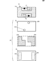
(実施形態1)
図1は実施形態1に係るESD保護デバイス1の正面断面図である。図2はESD保護デバイス1の各層の平面図である。ESD保護デバイス1は、CSP(Chip Size Package)タイプのデバイスであり、ダイオードおよびツェナーダイオードを含むESD保護回路10Aが構成されたSi基板10に、複数の樹脂層等を含む再配線層20が形成されている。Si基板10は、本発明に係る半導体基板に相当するが、本発明に係る半導体基板はSi基板には限定されず、GaAs基板などであってもよい。
(Embodiment 1)
FIG. 1 is a front sectional view of an ESD protection device 1 according to the first embodiment. FIG. 2 is a plan view of each layer of the ESD protection device 1. The ESD protection device 1 is a CSP (Chip Size Package) type device, and a rewiring
図3はSi基板10に形成されたESD保護回路10Aを示す図である。Si基板10について、図1〜図3を参照して説明する。
FIG. 3 is a diagram showing an
Si基板10の表面には素子形成領域11,12,13が設けられている。具体的には、p+型基板にpエピタキシャル層が形成され、このpエピタキシャル層内にnウェル、pウェルが順に形成され、これらのウェルとp拡散層またはn拡散層によって、Si基板10にダイオードおよびツェナーダイオードが形成されている。本実施形態では、図3に示すように、三つのダイオードが順方向を揃えて並列接続された各ダイオードD1,D2,D3,D4とツェナーダイオードDzとが形成されている。ダイオードD1,D2,D3,D4およびツェナーダイオードDzは、本発明に係る機能素子に相当する。
ダイオードD1,D2は順方向が揃って直列接続され、ダイオードD3,D4は順方向が揃って直列接続されている。また、ダイオードD1,D2およびダイオードD3,D4それぞれは、順方向が揃ってツェナーダイオードDzに対し並列接続されている。 The diodes D1 and D2 are connected in series with the forward direction aligned, and the diodes D3 and D4 are connected in series with the forward direction aligned. Further, the diodes D1, D2 and the diodes D3, D4 are aligned in the forward direction and connected in parallel to the Zener diode Dz.
Si基板10にはAlパッド(以下、パッドという。)P1,P2形成されている。パッドP1はダイオードD1,D2の接続点から引き出した位置に形成され、パッドP2はダイオードD3,D4の接続点から引き出した位置に形成されている。パッドP1,P2は、ESD保護回路10Aの入出力端であり、本発明に係る金属膜に相当する。
Al pads (hereinafter referred to as pads) P 1 and
図1に戻り、Si基板10の表層に形成された再配線層20は、パッドP1,P2の一部を覆うように、Si基板10の表面に形成されたSiN保護膜(保護膜層)21を含んでいる。SiN保護膜21は、Si基板10の表面にスパッタリングされ、エッチングにより開口が形成されている。スパッタリングにより形成されるSiN保護膜21の表面には、その成膜原理上、凹凸が現れる。なお、SiN保護膜21の比誘電率は7〜8と比較的高い。
Returning to FIG. 1, the
また、再配線層20は、Si基板10に形成された樹脂層22を含んでいる。この樹脂層22には、SiN保護膜21に形成された開口の位置に開口(コンタクトホール)22A,22B(図2参照)が形成されている。パッドP1,P2は、開口22A,22Bにより露出した状態となり、開口22A,22Bに形成される電極と導通する。樹脂層22は、SiN保護膜21よりも誘電率が低いエポキシ系(またはポリイミド系)の樹脂であり、その比誘電率は2〜6である。表面に凹凸があるSiN保護膜21を覆うように樹脂層22を形成することで、後述の電極が形成される樹脂層22の表面を平滑化(レベリング)できる。
The
また、SiN保護膜21はスパッタリングにより形成されるため、開口を形成する場合、その開口周辺は、厚みが薄く、開口(コンタクトホール)から平面方向に沿って離れるに従い平滑な状態に近づく。すなわち、SiN保護膜21は、パッドP1,P2周辺(コンタクトホール周辺)では厚みが薄く、パッドP1,P2(コンタクトホール)から平面方向に沿って離れるに従い厚くなる。そして、SiN保護膜21を覆うように形成される樹脂層22は、パッドP1,P2周辺(コンタクトホール周辺)では厚く、パッドP1,P2(コンタクトホール)から平面方向に沿って離れるに従い薄くなる。
Further, since the SiN
再配線層20はCu/Ti電極23A,23BおよびAu/Ni電極24A,24Bを含んでいる。Cu/Ti電極23A,23BおよびAu/Ni電極24A,24Bは、スパッタリングにより成膜され、樹脂層22の表面および開口22A,22Bに形成されている。Cu/Ti電極23A,23BおよびAu/Ni電極24A,24Bのうち、開口22A,22Bに形成された部分がパッドP1,P2に導通している。以下では、Cu/Ti電極23AおよびAu/Ni電極24A、ならびに、Cu/Ti電極23BおよびAu/Ni電極24Bそれぞれを端子電極25A,25Bと表す。この端子電極25A,25Bは、ESD保護デバイス1の入出力電極である。
The
再配線層20は、樹脂層22にさらに形成された樹脂層26を含んでいる。樹脂層26は、例えば低誘電率のエポキシ樹脂の層である。樹脂層26のうち、ESD保護デバイス1の入出力端とする端子電極25A,25Bの一部と対向する部分には、矩形状の開口26A,26Bが形成されている。
The
このように構成されたESD保護デバイス1において、Si基板10(またはESD保護回路10A)と端子電極25A,25Bとの間には寄生容量が発生する。しかしながら、Si基板10と端子電極25A,25Bとの間には低誘電率の樹脂層22が形成されているため、発生する寄生容量を抑制できる。また、表面に凹凸が現れるSiN保護膜21を樹脂層22でレベリングしているため、Si基板10と端子電極25A,25Bとの距離のばらつきをなくすことができる。このため、発生する寄生容量のばらつきを抑制できる。その結果、ESD保護デバイス1を設けた高周波回路のインピーダンスのずれを軽減でき、高周波回路の信号ロスを軽減できる。
In the ESD protection device 1 configured as described above, parasitic capacitance is generated between the Si substrate 10 (or the
なお、本実施形態では、Si基板10にツェナーダイオードDzなど形成して、ESD保護回路10Aを構成した例を示したが、例えば、可変容量素子等をSi基板10に形成して、それを用いた回路を構成してもよい。
In the present embodiment, an example is shown in which the Zener diode Dz or the like is formed on the
以下に、Si基板10にESD保護回路を形成する際のSi基板10の構造の例について説明する。図2に示す構造は、Si基板10の表面にダイオードD1〜D4を形成し、ツェナーダイオードDzをSi基板10の厚み方向に形成している。
Hereinafter, an example of the structure of the
図4は、Si基板10にESD保護回路を形成する際における第1の構造例を示す図である。図5は、図4に示す第1の構造例のSi基板10の模式図である。
FIG. 4 is a diagram showing a first structure example when forming an ESD protection circuit on the
この第1の構造例では、Si基板10はp+型基板であって、このp+型基板にSTI(Shallow Trench Isolation)法により素子分離膜110が形成されている。素子分離膜110で形成された領域それぞれには、ダイオードD1〜D4およびツェナーダイオードDzが形成されている。詳しくは、nエピタキシャル層が形成され、n+拡散層によって、Si基板10の厚み方向にダイオードD2,D4が形成されている。また、pウェルが形成され、n+拡散層によって、Si基板10の厚み方向にツェナーダイオードDzが形成されている。さらに、nエピタキシャル層内にnウェルが形成され、p+拡散層およびn+拡散層によって、Si基板10の表面にダイオードD1,D3が形成されている。
In the first structural example, the
Si基板10の表面には、SiO2膜111が形成され、ダイオードD1,D2が形成された領域を跨ぐようにパッドP1が形成され、ダイオードD3,D4が形成された領域を跨ぐようにパッドP2が形成されている。さらに、ダイオードD1,D3およびパッドP1,P2の形成領域以外のSi基板10の表面には、Al電極10Bが形成されている。Al電極10Bは、ダイオードD1,D3およびツェナーダイオードDzが形成された領域を跨ぐように形成されている。
A SiO 2 film 111 is formed on the surface of the
このように形成されたESD保護回路は、図3と同様である。なお、図3では、ダイオードD1〜D4はそれぞれ、順方向を揃えて並列接続された三つのダイオードであるが、図4では、ダイオードD1〜D4はそれぞれ一つのダイオードである。 The ESD protection circuit formed in this way is the same as that shown in FIG. In FIG. 3, the diodes D <b> 1 to D <b> 4 are three diodes connected in parallel with the forward direction aligned, but in FIG. 4, the diodes D <b> 1 to D <b> 4 are each one diode.
図6は、図4に示す第1の構造例のSi基板10を有するESD保護デバイスの各層の平面図である。Si基板10に形成された再配線層20に含まれる樹脂層22には、開口(コンタクトホール)22A,22Bが形成されている。パッドP1,P2は、開口22A,22Bにより露出した状態となり、開口22A,22Bに形成される電極と導通する。
FIG. 6 is a plan view of each layer of the ESD protection device having the
また、再配線層20は、樹脂層22の表面および開口22A,22Bに形成された端子電極25A,25Bを含んでいる。この端子電極25A,25Bは、図1で説明したCu/Ti電極およびAu/Ni電極を含む。端子電極25A,25Bは、ESD保護デバイス1の厚み方向において、Si基板10に形成されたツェナーダイオードを覆うように形成されている。これにより、ツェナーダイオードからのノイズの輻射が防止される。再配線層20の樹脂層26のうち、ESD保護デバイス1の入出力端とする端子電極25A,25Bの一部と対向する部分には、矩形状の開口26A,26Bが形成されている。
The
なお、端子電極25A,25Bは、図7に示す形状であってもよい。図7は、図6とは別の例のESD保護デバイスの各層の平面図である。この例では、端子電極25A,25Bは、Al電極10Bのほぼ全体(ツェナーダイオードの形成領域)を覆っている。この場合、図6の場合と比べて、ツェナーダイオードからのノイズの輻射がさらに防止される。
The
図8は、Si基板10にESD保護回路を形成する際における第2の構造例を示す図である。この第2の構造例では、第1の構造例と同様に、Si基板10の厚み方向に、ダイオードD2,D4およびツェナーダイオードDzが形成されている。そして、Si基板10の表面には、ダイオードD1a,D1b(ダイオードD1)およびダイオードD3a,D3b(ダイオードD3)が形成されている。さらに、Si基板10の表面には、パッドP1,P2およびAl電極10Bが形成されている。
FIG. 8 is a diagram illustrating a second structure example when forming an ESD protection circuit on the
このように形成されたESD保護回路は、図3と同様である。なお、図3では、ダイオードD1〜D4はそれぞれ、順方向を揃えて並列接続された三つのダイオードであるが、図8では、ダイオードD1,D3はそれぞれ二つのダイオードであり、ダイオードD2,D4は一つのダイオードである。 The ESD protection circuit formed in this way is the same as that shown in FIG. In FIG. 3, the diodes D1 to D4 are three diodes connected in parallel in the forward direction, but in FIG. 8, the diodes D1 and D3 are two diodes, and the diodes D2 and D4 are One diode.
図9は、図8に示す第2の構造例のSi基板10を有するESD保護デバイスの各層の平面図である。Si基板10に形成された再配線層20に含まれる樹脂層22には、開口(コンタクトホール)22A,22Bが形成されている。パッドP1,P2は、開口22A,22Bにより露出した状態となり、開口22A,22Bに形成される電極と導通する。
FIG. 9 is a plan view of each layer of the ESD protection device having the
また、再配線層20は、樹脂層22の表面および開口22A,22Bに形成された端子電極25A,25Bを含んでいる。この端子電極25A,25Bは、図1で説明したCu/Ti電極およびAu/Ni電極を含む。端子電極25A,25Bは、ESD保護デバイス1の厚み方向において、Si基板10に形成されたツェナーダイオードを覆うように形成されている。これにより、ツェナーダイオードからのノイズの輻射が防止される。再配線層20の樹脂層26のうち、ESD保護デバイス1の入出力端とする端子電極25A,25Bの一部と対向する部分には、矩形状の開口26A,26Bが形成されている。
The
これら第1の構造例および第2の構造例では、Si基板10の厚み方向にダイオードおよびツェナーダイオードを形成しているため、それらをSi基板10の表面に形成した場合と比べて、ESL成分を軽減できる。
In the first structure example and the second structure example, diodes and Zener diodes are formed in the thickness direction of the
以下に、本実施形態に係るESD保護デバイス1の接続例および動作原理を説明する。 Hereinafter, a connection example and an operation principle of the ESD protection device 1 according to the present embodiment will be described.
図10Aおよび図10Bは、本実施形態に係るESD保護デバイス1の接続例を示す図である。ESD保護デバイス1は電子機器に搭載される。電子機器の例として、ノートPC、タブレット型端末装置、携帯電話機、デジタルカメラ、携帯型音楽プレーヤなどが挙げられる。 10A and 10B are diagrams illustrating a connection example of the ESD protection device 1 according to the present embodiment. The ESD protection device 1 is mounted on an electronic device. Examples of electronic devices include notebook PCs, tablet terminal devices, mobile phones, digital cameras, and portable music players.
図10Aでは、I/Oポート100と保護すべきIC101とを接続する信号ラインと、GNDとの間にESD保護デバイス1を接続した例を示す。I/Oポート100は、例えばアンテナが接続されるポートである。本実施形態に係るESD保護デバイス1は双方向型であって、第1入出力端および第2入出力端の何れが入力側であってもよい。例えば第1入出力端を入力側とした場合、信号ラインに第1入出力端が接続され、第2入出力端がGNDに接続される。
FIG. 10A shows an example in which the ESD protection device 1 is connected between the signal line connecting the I /
図10Bでは、コネクタ102とIC101とを接続する信号ラインと、GNDラインとの間にESD保護デバイス1を接続した例を示す。この例の信号ラインは、例えば、高速伝送線路(差動伝送線路)であって、複数の信号ラインそれぞれと、GNDラインとの間にESD保護デバイス1が接続されている。
FIG. 10B shows an example in which the ESD protection device 1 is connected between the signal line connecting the
図11および図12は、本実施形態に係るESD保護デバイスの動作原理を説明するための図である。 11 and 12 are diagrams for explaining the operation principle of the ESD protection device according to the present embodiment.
図11は、第1入出力端(端子電極25A)に繋がるパッドP1から、第2入出力端(端子電極25B)に繋がるパッドP2へ電流が流れる場合を説明するための図である。ツェナーダイオードDzのツェナー電圧を超えるサージ電圧が印加されると、図中破線で示すように、第1入力端から入ってきたサージ電流は、パッドP1からダイオードD1、ツェナーダイオードDzおよびダイオードD4の経路を流れ、パッドP2からグランドへ放電される。
FIG. 11 is a diagram for explaining a case where a current flows from the pad P1 connected to the first input / output terminal (
図12は、第2入出力端(端子電極25B)に繋がるパッドP2から、第1入出力端(端子電極25A)に繋がるパッドP1へ電流が流れる場合を説明するための図である。この場合、図中破線で示すように、第2入力端から入ってきたサージ電流は、パッドP2からダイオードD3、ツェナーダイオードDzおよびダイオードD2の経路を流れ、パッドP1からグランドへ放電される。
FIG. 12 is a diagram for explaining a case where a current flows from the pad P2 connected to the second input / output terminal (
なお、図6に示す第1の構造例または図8に示す第2の構造例を有するESD保護デバイスでは、Al電極10Bと端子電極25A,25Bとの間に容量が発生する。この容量は、ツェナーダイオードにかかる高周波電圧を、Al電極10Bから端子電極25A(または25B)およびパッドP1(またはP2)を介してグランドへバイパスする。この高周波電圧のバイパスにより、ESDのピーク電圧を低くできる。
In the ESD protection device having the first structural example shown in FIG. 6 or the second structural example shown in FIG. 8, a capacitance is generated between the Al electrode 10B and the
以下に、ESD保護デバイスの製造工程について説明する。 Below, the manufacturing process of an ESD protection device is demonstrated.
図13はESD保護デバイス1の製造工程を示す図である。なお、図13において、形成時にSiN保護膜21の表面に現れる凹凸の図示は省略している。
FIG. 13 is a diagram illustrating a manufacturing process of the ESD protection device 1. In FIG. 13, the unevenness appearing on the surface of the SiN
ESD保護デバイス1は次の工程で製造される。 The ESD protection device 1 is manufactured by the following process.
(A)まず、ESD保護回路10Aが形成されたSi基板10に、ESD保護回路10Aと導通するパッドP1,P2がフォトリソグラフィにより形成される。また、基板表面にSiN保護膜21がスパッタリングされ、エッチングにより開口21A,21Bが形成される。
(A) First, pads P1 and P2 that are electrically connected to the
なお、パッドP1,P2は、それらの面積を小さくすることで、対向する基板(ESD保護回路10A)との間に形成される寄生容量を小さくできる。この寄生容量を小さくすることで、インピーダンスのずれを抑制でき、その結果、信号ラインにおける損失を低減できる。
Note that, by reducing the area of the pads P1 and P2, the parasitic capacitance formed between the opposing substrates (
(B)次に、Si基板10にエポキシ系ソルダージレストがスピンコーティングされて、樹脂層22が形成され、開口22A,22Bが形成される。この樹脂層22を形成することにより、端子電極25A,25Bを形成する表面をレベリングすることができる。
(B) Next, an epoxy solder girest is spin-coated on the
(C)樹脂層22の表面にCu/Ti電極23が約1.0μm/0.1μmの厚みでスパッタリングにより成膜され、その後、Au/Ni電極24A,24Bが約0.1μm/5.0μmの厚みでスパッタリングにより成膜される。なお、このAu/Ni電極24A,24Bは、マスキングにより一部にのみ形成される。
(C) A Cu /
(D)続いて、Cu/Ti電極23がウエットエッチングされて、Cu/Ti電極23A,23Bが形成される。これにより、端子電極25A,25Bが形成される。
(D) Subsequently, the Cu /
(E)その後、樹脂層22の表面にエポキシ系ソルダージレストがスピンコーティングにより樹脂層26が形成され、開口26A,26Bが形成される。
(E) Thereafter, the
(実施形態2)
以下、実施形態2に係るESD保護デバイスについて、実施形態1と相違する点についてのみ説明する。
(Embodiment 2)
Hereinafter, only the points different from the first embodiment of the ESD protection device according to the second embodiment will be described.
図14は実施形態2に係るESD保護デバイス2の正面断面図である。図15は、ESD保護デバイス2の各層の平面図である。なお、図15では、Si基板10に形成されたESD保護回路10Aの具体的な構成は省略した図としている。
FIG. 14 is a front sectional view of the
ESD保護デバイス2はSi基板10に再配線層30が形成されてなる。Si基板10、Si基板10に形成されたESD保護回路10AおよびパッドP1,P2は、実施形態1と同じである。
The
Si基板10にはSiN保護膜21が形成される。再配線層30は、SiN保護膜21の凹凸をレベリングする樹脂層22を含んでいる。実施形態1と同様に、SiN保護膜21は、コンタクトホール(開口22A,22B)周辺では厚みが薄く、コンタクトホールから平面方向に沿って離れるに従い厚くなる。そして、SiN保護膜21を覆うように形成される樹脂層22は、コンタクトホール周辺では厚く、コンタクトホールから平面方向に沿って離れるに従い薄くなる。
A SiN
SiN保護膜21および樹脂層22に形成された開口および樹脂層22の表面には、パッドP1,P2と導通する中間配線電極27A,27Bが形成されている。この中間配線電極27A,27Bは、Ti/Cu/Ti電極である。中間配線電極27A,27Bは、図15の平面視において、パッドP1,P2と重なる部分から平面方向に離れるに従い幅狭となる形状を有している。また、この中間配線電極27A,27Bは、スパッタリングにより成膜形成されている。
再配線層30は、樹脂層22にさらに形成された樹脂層28および端子電極29A,29Bを含んでいる。この樹脂層28にも、樹脂層22と同様に、中間配線電極27A,27Bにおける幅が狭くなっている側の端部(以下、狭幅部という。)と対向する部分に開口28A,28Bが形成されている。端子電極29A,29Bは、Cu/Ti電極およびAu/Ni電極をスパッタリングすることにより成膜され、樹脂層28の表面および開口(ビアホール)28A,28Bに形成される。端子電極29A,29Bのうち、開口28A,28Bに形成された部分は、中間配線電極27A,27Bの狭幅部に導通している。この端子電極29A,29Bは、ESD保護デバイス2の入出力電極である。
The
さらに、再配線層30は、樹脂層28にさらに形成された樹脂層31を含んでいる。樹脂層31は低誘電率のエポキシ樹脂の層である。樹脂層31のうち端子電極29A,29Bの一部と対向する部分には、矩形状の開口31A,31B,31C,31Dが形成されている。これらの樹脂層28,31は、樹脂層22,26と同一の材料・製法により形成される。
Further, the
なお、開口31A,31B,31C,31Dは、樹脂層28のビアホールの位置を避けて形成されることが好ましい。端子電極29A,29Bのビアホール部分は、製造工程において窪み(図14では省略)が生じる場合がある。開口31A,31B,31C,31Dからこの窪みが露出している場合、開口31A,31B,31C,31Dで半田付けすると、この窪みに空気がたまり、接続信頼性の低下するおそれがある。このため、ビアホールの位置を避けて開口31A,31B,31C,31Dを形成することで、接続信頼性の低下を防止できる。
The
このように形成されたESD保護デバイス2において、実施形態1と同様に、Si基板10(またはESD保護回路10A)と中間配線電極27A,27Bとの間に発生する寄生容量を少なくでき、また、発生する寄生容量のばらつきを軽減できる。さらに、低誘電率の樹脂層22が間に介在することでSi基板10と端子電極29A,29Bとの間に発生する寄生容量をも抑制することができる。
In the
また、本実施形態に係る中間配線電極27A,27Bは、平面視において、パッドP1,P2と重なる部分から離れるに従い幅狭となる形状である。したがって、幅が一定である、例えば矩形状とした場合と比べて、Si基板10と中間配線電極27A,27Bとの対向面積は小さくなり、寄生容量も小さくなる。このため、コンタクトホール(開口22A,22B)から平面方向に沿って離れるに従い低誘電率の樹脂層22は薄くなるが、Si基板10と中間配線電極27A,27Bとの対向面積を小さくすることで、寄生容量が大きくなることを抑制できる。
Further, the
なお、Si基板10との対向面積を小さくするための中間配線電極27A,27Bの形状は、図15の形状に限らない。図16は、中間配線電極の異なる形状の例を示す平面図である。図16に示す中間配線電極27C,27Dは、パッドP1,P2に導通させるコンタクトホール部分と、端子電極29A,29Bと導通させるビアホール部分とが円形状であり、それらを繋ぐ電極が細線状とした形状である。これにより、Si基板10と中間配線電極27C,27Dとの対向面積は小さくなり、寄生容量も小さくなる。なお、これらの中間配線電極27C,27Dは、中間配線電極27A,27B同様、スパッタリングにより、Ti/Cu/Ti電極として形成されている。
Note that the shape of the
実施形態2に係るESD保護デバイス2の動作原理および製造工程については、実施形態1と同様であるため、説明は省略する。
Since the operation principle and manufacturing process of the
以下、実施形態2に係るESD保護デバイス2の様々な変形例について順に説明する。図17、図18および図19は、実施形態2に係るESD保護デバイスの各変形例を示す図である。図17、図18および図19は、Si基板10に形成されるESD保護回路10Aの構成を模式的に示している。具体的な構成は、図2に示す構成と同一である。
Hereinafter, various modifications of the
図17では、コンタクトホールとビアホールとの平面視した場合の位置関係が、図14に示す場合と異なる例を示す。中間配線電極27E,27Fは、中間配線電極27A,27Bと同形状であるが、ESD保護デバイスの外側から内側に向かって幅狭となっている。すなわち、中間配線電極27E,27Fのコンタクトホールが、端子電極29C,29Dのビアホールの内側に形成されている。そして、樹脂層31のうち端子電極29C,29Dの一部と対向する部分には、矩形状の開口31E,31Fが形成されている。
FIG. 17 shows an example in which the positional relationship between the contact hole and the via hole in a plan view is different from that shown in FIG. The
図18は、Si基板10に形成されている再配線層40の樹脂層数が、図14に示す場合よりも増加した例を示す。この例では、再配線層40は、樹脂層28の開口28A,28Bおよびその表面に形成された中間配線電極27G,27Hを含んでいる。この中間配線電極27G,27Hは、中間配線電極27A,27Bと同形状であり、狭幅部が導通している。
FIG. 18 shows an example in which the number of resin layers of the
また、再配線層40は、樹脂層28に形成された樹脂層32を含んでいる。この樹脂層32には開口32A,32Bが形成されていて、その開口32A,32Bおよび樹脂層32の表面に端子電極29E,29Fが形成されている。端子電極29E,29Fは、中間配線電極27G,27Hと導通している。そして、樹脂層32には、開口34A,34Bが形成された樹脂層34がさらに形成されている。開口34A,34Bは、端子電極29E,29Fの一部と対向する位置に形成されている。
The
図19は、中間配線電極が図14に示す中間配線電極27A,27Bと異なる形状とした例を示す。この例に示す再配線層50は中間配線電極35A,35Bを含んでいる。中間配線電極35A,35Bは、樹脂層22の開口22A,22Bおよび樹脂層22の表面に形成されている。中間配線電極35A,35Bは、中央部にコンタクトホールを有し、パッドP1,P2と導通している。また、中間配線電極35A,35Bは、両端部に狭幅部を有している。
FIG. 19 shows an example in which the intermediate wiring electrode has a different shape from the
樹脂層22に形成される樹脂層28には、四つの開口28C,28D,28E,28Fが形成されている。開口28C,28Eおよび樹脂層28の表面には端子電極29Gが形成され、開口28D,28Fおよび樹脂層28の表面には端子電極29Hが形成されている。端子電極29G,29Hのうち、開口28C,28D,28E,28Fに形成されている部分は中間配線電極35A,35Bと導通している。
The
以上説明した図17〜図19のESD保護デバイスも、実施形態1,2と同様、Si基板10にSiN保護膜21と、SiN保護膜21より低誘電率の樹脂層22とが形成されている。このため、Si基板10と中間配線電極との間に発生する寄生容量を軽減できる。また、Si基板10と中間配線電極との距離のばらつきをなくすことで、発生する寄生容量のばらつきをも抑制できる。その結果、ESD保護デバイスを設けた高周波回路のインピーダンスのずれを軽減でき、高周波回路の信号ロスを軽減できる。
17 to 19 described above, the SiN
なお、図17〜図19において、中間配線電極27E,27F,27G,27H,35A,35Bは、中間配線電極27A,27Bと同様、スパッタリングにより、Ti/Cu/Ti電極として形成されている。また、端子電極29C,29D,29E,29F,29G,29Hは、端子電極29A,29Bと形状が異なるものの、端子電極29A,29Bと同一の材料・製法により形成される。各樹脂層31,32,34は、樹脂層22,26と同じ製法により形成される。
17 to 19, the
また、上述の実施形態では、ツェナーダイオードを有するESD保護デバイスについて説明したが、これに限定されず、ESD保護デバイスは、例えばPNP型半導体、またはNPN型半導体を有したものであってもよい。 Moreover, although the ESD protection device which has a Zener diode was demonstrated in the above-mentioned embodiment, it is not limited to this, For example, the ESD protection device may have a PNP type semiconductor or an NPN type semiconductor.
1,2−ESD保護デバイス(半導体装置)
10−Si基板(半導体基板)
10A−ESD保護回路
11,12,13−素子形成領域
20,30,40,50−再配線層
21−SiN保護膜
22,26,28,31,32,34−樹脂層
22A,22B−開口
23A,23B−Cu/Ti電極
24A,24B−Au/Ni電極
25A,25B−端子電極
26A,26B−開口
27A,27B,27C,27D,27E,27F、27G,27H−中間配線電極
28A,28B,28C,28D,28E,28F−開口
29A,29B,29C,29D,29E,29F,29G,29H−端子電極
31A,31B,31C,31D,31E,31F−開口
32A,32B−開口
34A,34B−開口
35A,35B−中間配線電極
D1,D2,D3,D4−ダイオード(機能素子)
Dz−ツェナーダイオード(機能素子)
P1−パッド(金属膜)
P2−パッド(金属膜)
1,2-ESD protection device (semiconductor device)
10-Si substrate (semiconductor substrate)
10A-
Dz-Zener diode (functional element)
P1- pad (metal film)
P2- pad (metal film)
Claims (2)
前記半導体基板の表面に形成され、前記機能素子と導通している金属膜と、
前記半導体基板の表面と対向している配線電極と、前記金属膜および前記配線電極の一部を導通させるコンタクトホールとを含む再配線層と、
を備え、
前記再配線層は、
前記コンタクトホールが接している領域以外の前記金属膜および前記半導体基板の表面を覆うように、前記半導体基板の表面に形成された保護膜層と、
前記保護膜層より誘電率が低く、前記保護膜層を覆うように、前記保護膜層および前記配線電極の間に形成された樹脂層と、
を含み、
前記保護膜層の断面形状は、前記配線電極と対向する範囲内で、前記コンタクトホールから前記半導体基板の表面に沿って離れるに従い厚くなる形状であり、
前記樹脂層の断面形状は、前記配線電極と対向する範囲内で、前記コンタクトホールから前記半導体基板の表面に沿って離れて前記保護膜層が厚くなるに従い薄くなる形状であり、
前記配線電極の平面形状は、前記コンタクトホールが接している領域から前記半導体基板の表面に沿って離れるに従い幅が徐々に細くなる先細り形状である、
半導体装置。 A semiconductor substrate on which functional elements are formed;
A metal film formed on the surface of the semiconductor substrate and electrically connected to the functional element;
A rewiring layer including a wiring electrode facing the surface of the semiconductor substrate, and a contact hole for conducting a part of the metal film and the wiring electrode;
With
The rewiring layer is
A protective film layer formed on the surface of the semiconductor substrate so as to cover the surface of the semiconductor film and the metal film other than the region in contact with the contact hole;
A dielectric constant lower than that of the protective film layer, and a resin layer formed between the protective film layer and the wiring electrode so as to cover the protective film layer;
Including
The cross-sectional shape of the protective film layer is a shape that becomes thicker as the distance from the contact hole along the surface of the semiconductor substrate is within a range facing the wiring electrode,
The cross-sectional shape of the resin layer is a shape that becomes thinner as the protective film layer becomes thicker away from the contact hole along the surface of the semiconductor substrate within a range facing the wiring electrode,
The planar shape of the wiring electrode is a tapered shape in which the width gradually decreases as the distance from the region in contact with the contact hole along the surface of the semiconductor substrate increases.
Semiconductor device.
前記半導体基板の表面に形成され、前記ESD保護回路に接続された金属膜と、
前記半導体基板の表面と対向している配線電極と、前記金属膜および前記配線電極の一部を導通させるコンタクトホールとを含む再配線層と、
を備え、
前記再配線層は、
前記コンタクトホールが接している領域以外の前記金属膜および前記半導体基板の表面を覆うように、前記半導体基板の表面に形成された保護膜層と、
前記保護膜層より誘電率が低く、前記保護膜層を覆うように、前記保護膜層および前記配線電極の間に形成された樹脂層と、
を含み、
前記保護膜層の断面形状は、前記配線電極と対向する範囲内で、前記コンタクトホールから前記半導体基板の表面に沿って離れるに従い厚くなる形状であり、
前記樹脂層の断面形状は、前記配線電極と対向する範囲内で、前記コンタクトホールから前記半導体基板の表面に沿って離れて前記保護膜層が厚くなるに従い薄くなる形状であり、
前記配線電極の平面形状は、前記コンタクトホールが接している領域から前記半導体基板の表面に沿って離れるに従い幅が徐々に細くなる先細り形状である、
ESD保護デバイス。 A semiconductor substrate on which an ESD protection circuit is formed;
Wherein formed on the semiconductor substrate surface, and a metal film connected to the ESD protection circuit,
A rewiring layer including a wiring electrode facing the surface of the semiconductor substrate, and a contact hole for conducting a part of the metal film and the wiring electrode;
With
The rewiring layer is
A protective film layer formed on the surface of the semiconductor substrate so as to cover the surface of the semiconductor film and the metal film other than the region in contact with the contact hole;
A dielectric constant lower than that of the protective film layer, and a resin layer formed between the protective film layer and the wiring electrode so as to cover the protective film layer;
Including
The cross-sectional shape of the protective film layer is a shape that becomes thicker as the distance from the contact hole along the surface of the semiconductor substrate is within a range facing the wiring electrode,
The cross-sectional shape of the resin layer is a shape that becomes thinner as the protective film layer becomes thicker away from the contact hole along the surface of the semiconductor substrate within a range facing the wiring electrode,
The planar shape of the wiring electrode is a tapered shape in which the width gradually decreases as the distance from the region in contact with the contact hole along the surface of the semiconductor substrate increases.
ESD protection device.
Applications Claiming Priority (4)
| Application Number | Priority Date | Filing Date | Title |
|---|---|---|---|
| JP2013039379 | 2013-02-28 | ||
| JP2013039379 | 2013-02-28 | ||
| JP2013079960 | 2013-04-05 | ||
| JP2013079960 | 2013-04-05 |
Related Parent Applications (1)
| Application Number | Title | Priority Date | Filing Date |
|---|---|---|---|
| JP2015502921A Division JPWO2014132938A1 (en) | 2013-02-28 | 2014-02-25 | Semiconductor device and ESD protection device |
Publications (2)
| Publication Number | Publication Date |
|---|---|
| JP2017118110A JP2017118110A (en) | 2017-06-29 |
| JP6265256B2 true JP6265256B2 (en) | 2018-01-24 |
Family
ID=51428202
Family Applications (2)
| Application Number | Title | Priority Date | Filing Date |
|---|---|---|---|
| JP2015502921A Pending JPWO2014132938A1 (en) | 2013-02-28 | 2014-02-25 | Semiconductor device and ESD protection device |
| JP2016245074A Active JP6265256B2 (en) | 2013-02-28 | 2016-12-19 | Semiconductor device and ESD protection device |
Family Applications Before (1)
| Application Number | Title | Priority Date | Filing Date |
|---|---|---|---|
| JP2015502921A Pending JPWO2014132938A1 (en) | 2013-02-28 | 2014-02-25 | Semiconductor device and ESD protection device |
Country Status (5)
| Country | Link |
|---|---|
| US (2) | US9607976B2 (en) |
| JP (2) | JPWO2014132938A1 (en) |
| CN (1) | CN105051887B (en) |
| GB (1) | GB2525774A (en) |
| WO (1) | WO2014132938A1 (en) |
Families Citing this family (16)
| Publication number | Priority date | Publication date | Assignee | Title |
|---|---|---|---|---|
| CN105051887B (en) | 2013-02-28 | 2018-04-17 | 株式会社村田制作所 | Semiconductor device |
| CN205452284U (en) | 2013-04-05 | 2016-08-10 | 株式会社村田制作所 | ESD protection device |
| US9666576B2 (en) * | 2014-11-13 | 2017-05-30 | Mediatek Inc. | Electrostatic discharge (ESD) protection device |
| JP6532848B2 (en) | 2016-09-15 | 2019-06-19 | 株式会社東芝 | Semiconductor device |
| US10276518B2 (en) * | 2017-03-21 | 2019-04-30 | Taiwan Semiconductor Manufacturing Company Limited | Semiconductor arrangement in fan out packaging including magnetic structure around transmission line |
| US10578800B2 (en) * | 2017-06-06 | 2020-03-03 | Sifotonics Technologies Co., Ltd. | Silicon photonic integrated circuit with electrostatic discharge protection mechanism for static electric shocks |
| BR112019025042A2 (en) | 2017-06-15 | 2020-06-16 | Nippon Steel Corporation | LAMINATED STEEL FOR SPRING STEEL |
| WO2019031036A1 (en) * | 2017-08-10 | 2019-02-14 | 株式会社村田製作所 | Esd protection device and signal transmission line |
| TWI745595B (en) * | 2018-06-05 | 2021-11-11 | 源芯半導體股份有限公司 | Electrostatic discharge protection device |
| JP7055534B2 (en) * | 2018-09-10 | 2022-04-18 | 株式会社東芝 | Manufacturing method of semiconductor device |
| JP7154913B2 (en) | 2018-09-25 | 2022-10-18 | 株式会社東芝 | Semiconductor device and its manufacturing method |
| FR3094838B1 (en) | 2019-04-05 | 2022-09-16 | St Microelectronics Tours Sas | Device for protection against electrostatic discharges |
| FR3094837B1 (en) * | 2019-04-05 | 2022-09-09 | St Microelectronics Tours Sas | Device for protection against electrostatic discharges |
| CN110265392B (en) * | 2019-06-06 | 2024-05-31 | 江苏吉莱微电子股份有限公司 | An integrated low-capacitance ESD protection device and preparation method thereof |
| CN118043968A (en) * | 2021-10-04 | 2024-05-14 | 株式会社村田制作所 | Transient voltage absorbing element |
| US12034000B2 (en) * | 2022-03-23 | 2024-07-09 | Nxp B.V. | Double IO pad cell including electrostatic discharge protection scheme with reduced latch-up risk |
Family Cites Families (54)
| Publication number | Priority date | Publication date | Assignee | Title |
|---|---|---|---|---|
| JP2906576B2 (en) | 1990-05-11 | 1999-06-21 | 日産自動車株式会社 | Semiconductor device |
| JP2924088B2 (en) * | 1990-05-23 | 1999-07-26 | 日本電気株式会社 | Semiconductor device |
| FR2683947B1 (en) | 1991-11-18 | 1994-02-18 | Sgs Thomson Microelectronics Sa | LOW VOLTAGE LOW VOLTAGE MONOLITHIC PROTECTION DIODE. |
| JPH05268123A (en) | 1992-03-19 | 1993-10-15 | Fujitsu Ltd | Bidirectional power supply circuit |
| JP2774906B2 (en) | 1992-09-17 | 1998-07-09 | 三菱電機株式会社 | Thin semiconductor device and method of manufacturing the same |
| JPH1154708A (en) | 1997-08-06 | 1999-02-26 | Mitsubishi Electric Corp | Semiconductor integrated circuit device |
| JPH11175183A (en) * | 1997-12-12 | 1999-07-02 | Fujitsu Ltd | Clock distribution circuit in semiconductor integrated circuit |
| US6538300B1 (en) | 2000-09-14 | 2003-03-25 | Vishay Intertechnology, Inc. | Precision high-frequency capacitor formed on semiconductor substrate |
| JP2002198374A (en) * | 2000-10-16 | 2002-07-12 | Sharp Corp | Semiconductor device and its fabrication method |
| JP2002252309A (en) | 2001-02-23 | 2002-09-06 | Denso Corp | Structure and method for packaging semiconductor chip |
| JP2002262309A (en) | 2001-03-02 | 2002-09-13 | Sanyo Electric Co Ltd | Three-dimensional photographing device and three- dimensional shape measurement system |
| JP2002270720A (en) | 2001-03-09 | 2002-09-20 | Matsushita Electric Ind Co Ltd | Semiconductor device and its manufacturing method |
| JP4963148B2 (en) | 2001-09-18 | 2012-06-27 | ルネサスエレクトロニクス株式会社 | Manufacturing method of semiconductor device |
| JP2003124222A (en) | 2001-10-11 | 2003-04-25 | Hitachi Ltd | Semiconductor device |
| JP3778152B2 (en) | 2002-09-27 | 2006-05-24 | 株式会社デンソー | diode |
| JP3945380B2 (en) * | 2002-11-08 | 2007-07-18 | カシオ計算機株式会社 | Semiconductor device and manufacturing method thereof |
| US7285867B2 (en) * | 2002-11-08 | 2007-10-23 | Casio Computer Co., Ltd. | Wiring structure on semiconductor substrate and method of fabricating the same |
| JP2004281898A (en) * | 2003-03-18 | 2004-10-07 | Seiko Epson Corp | Semiconductor device and its manufacturing method, circuit board, and electronic equipment |
| JP3983205B2 (en) * | 2003-07-08 | 2007-09-26 | 沖電気工業株式会社 | Semiconductor device and manufacturing method thereof |
| US7291923B1 (en) * | 2003-07-24 | 2007-11-06 | Xilinx, Inc. | Tapered signal lines |
| JP2005340573A (en) * | 2004-05-28 | 2005-12-08 | Fujikura Ltd | Semiconductor element, manufacturing method thereof and semiconductor device |
| JP4735929B2 (en) | 2004-08-03 | 2011-07-27 | 株式会社村田製作所 | Dielectric thin film capacitor manufacturing method and dielectric thin film capacitor |
| JP2006141136A (en) | 2004-11-12 | 2006-06-01 | Yaskawa Electric Corp | Drive control device |
| JP4547247B2 (en) * | 2004-12-17 | 2010-09-22 | ルネサスエレクトロニクス株式会社 | Semiconductor device |
| US7781826B2 (en) | 2006-11-16 | 2010-08-24 | Alpha & Omega Semiconductor, Ltd. | Circuit configuration and manufacturing processes for vertical transient voltage suppressor (TVS) and EMI filter |
| US7880223B2 (en) | 2005-02-11 | 2011-02-01 | Alpha & Omega Semiconductor, Ltd. | Latch-up free vertical TVS diode array structure using trench isolation |
| US7571153B2 (en) | 2005-03-28 | 2009-08-04 | Microsoft Corporation | Systems and methods for performing streaming checks on data format for UDTs |
| US7468545B2 (en) * | 2005-05-06 | 2008-12-23 | Megica Corporation | Post passivation structure for a semiconductor device and packaging process for same |
| US7489488B2 (en) | 2005-10-19 | 2009-02-10 | Littelfuse, Inc. | Integrated circuit providing overvoltage protection for low voltage lines |
| JP2007123538A (en) | 2005-10-27 | 2007-05-17 | Matsushita Electric Ind Co Ltd | Semiconductor device for surge protection and manufacturing method thereof |
| TWI303872B (en) | 2006-03-13 | 2008-12-01 | Ind Tech Res Inst | High power light emitting device assembly with esd preotection ability and the method of manufacturing the same |
| JP2007294586A (en) * | 2006-04-24 | 2007-11-08 | Toshiba Corp | Semiconductor device |
| JP4267660B2 (en) * | 2006-12-05 | 2009-05-27 | 日本特殊陶業株式会社 | Multilayer wiring board and element mounting apparatus |
| JP5118982B2 (en) * | 2007-01-31 | 2013-01-16 | 三洋電機株式会社 | Semiconductor module and manufacturing method thereof |
| DE102007020656B4 (en) | 2007-04-30 | 2009-05-07 | Infineon Technologies Ag | Semiconductor chip workpiece, semiconductor device, and method of manufacturing a semiconductor chip workpiece |
| US7579632B2 (en) | 2007-09-21 | 2009-08-25 | Semiconductor Components Industries, L.L.C. | Multi-channel ESD device and method therefor |
| JP5301231B2 (en) | 2008-09-30 | 2013-09-25 | 株式会社テラミクロス | Semiconductor device |
| US8089095B2 (en) | 2008-10-15 | 2012-01-03 | Semiconductor Components Industries, Llc | Two terminal multi-channel ESD device and method therefor |
| JP2009016882A (en) | 2008-10-20 | 2009-01-22 | Panasonic Corp | Semiconductor device and manufacturing method thereof |
| JP4794615B2 (en) * | 2008-11-27 | 2011-10-19 | パナソニック株式会社 | Semiconductor device |
| JPWO2010100995A1 (en) * | 2009-03-02 | 2012-09-06 | 株式会社村田製作所 | Antifuse element |
| EP2414801B1 (en) * | 2009-03-30 | 2021-05-26 | QUALCOMM Incorporated | Chip package with stacked processor and memory chips |
| JP2010278040A (en) * | 2009-05-26 | 2010-12-09 | Renesas Electronics Corp | Semiconductor device manufacturing method and semiconductor device |
| US8710645B2 (en) | 2009-10-19 | 2014-04-29 | Jeng-Jye Shau | Area reduction for surface mount package chips |
| WO2011152255A1 (en) | 2010-06-02 | 2011-12-08 | 株式会社村田製作所 | Esd protection device |
| JP5532137B2 (en) | 2010-08-18 | 2014-06-25 | 株式会社村田製作所 | ESD protection device |
| US8217462B2 (en) | 2010-09-22 | 2012-07-10 | Amazing Microelectronic Corp. | Transient voltage suppressors |
| JP2012146717A (en) * | 2011-01-07 | 2012-08-02 | Toshiba Corp | Esd protection circuit |
| JP2012182381A (en) | 2011-03-02 | 2012-09-20 | Panasonic Corp | Semiconductor device |
| JP6037499B2 (en) | 2011-06-08 | 2016-12-07 | ローム株式会社 | Semiconductor device and manufacturing method thereof |
| TW201323478A (en) * | 2011-10-31 | 2013-06-16 | Corning Inc | Fused thiophenes, methods of making fused thiophenes, and uses thereof |
| CN105051887B (en) * | 2013-02-28 | 2018-04-17 | 株式会社村田制作所 | Semiconductor device |
| US9585768B2 (en) | 2013-03-15 | 2017-03-07 | DePuy Synthes Products, Inc. | Acetabular cup prosthesis alignment system and method |
| CN205452284U (en) | 2013-04-05 | 2016-08-10 | 株式会社村田制作所 | ESD protection device |
-
2014
- 2014-02-25 CN CN201480010622.0A patent/CN105051887B/en active Active
- 2014-02-25 WO PCT/JP2014/054406 patent/WO2014132938A1/en active Application Filing
- 2014-02-25 JP JP2015502921A patent/JPWO2014132938A1/en active Pending
- 2014-02-25 GB GB1510735.2A patent/GB2525774A/en not_active Withdrawn
-
2015
- 2015-08-27 US US14/837,153 patent/US9607976B2/en active Active
-
2016
- 2016-12-19 JP JP2016245074A patent/JP6265256B2/en active Active
-
2017
- 2017-02-08 US US15/427,195 patent/US9824955B2/en active Active
Also Published As
| Publication number | Publication date |
|---|---|
| GB2525774A (en) | 2015-11-04 |
| JPWO2014132938A1 (en) | 2017-02-02 |
| WO2014132938A1 (en) | 2014-09-04 |
| JP2017118110A (en) | 2017-06-29 |
| US20150364462A1 (en) | 2015-12-17 |
| CN105051887A (en) | 2015-11-11 |
| US9607976B2 (en) | 2017-03-28 |
| CN105051887B (en) | 2018-04-17 |
| GB201510735D0 (en) | 2015-08-05 |
| US20170148707A1 (en) | 2017-05-25 |
| US9824955B2 (en) | 2017-11-21 |
Similar Documents
| Publication | Publication Date | Title |
|---|---|---|
| JP6265256B2 (en) | Semiconductor device and ESD protection device | |
| JP6098697B2 (en) | Semiconductor device | |
| JP5796692B2 (en) | ESD protection device | |
| JP5617980B2 (en) | ESD protection device | |
| CN205452284U (en) | ESD protection device | |
| JP2014167987A (en) | Semiconductor device | |
| CN205282447U (en) | Semiconductor device | |
| JP6098230B2 (en) | Semiconductor device | |
| JP6048218B2 (en) | ESD protection device | |
| CN205282460U (en) | Semiconductor device and mounting structure |
Legal Events
| Date | Code | Title | Description |
|---|---|---|---|
| A131 | Notification of reasons for refusal |
Free format text: JAPANESE INTERMEDIATE CODE: A131 Effective date: 20170926 |
|
| A977 | Report on retrieval |
Free format text: JAPANESE INTERMEDIATE CODE: A971007 Effective date: 20170928 |
|
| A521 | Request for written amendment filed |
Free format text: JAPANESE INTERMEDIATE CODE: A523 Effective date: 20171106 |
|
| TRDD | Decision of grant or rejection written | ||
| A01 | Written decision to grant a patent or to grant a registration (utility model) |
Free format text: JAPANESE INTERMEDIATE CODE: A01 Effective date: 20171128 |
|
| A61 | First payment of annual fees (during grant procedure) |
Free format text: JAPANESE INTERMEDIATE CODE: A61 Effective date: 20171211 |
|
| R150 | Certificate of patent or registration of utility model |
Ref document number: 6265256 Country of ref document: JP Free format text: JAPANESE INTERMEDIATE CODE: R150 |