JP6262060B2 - Manufacturing method of semiconductor device - Google Patents
Manufacturing method of semiconductor device Download PDFInfo
- Publication number
- JP6262060B2 JP6262060B2 JP2014076974A JP2014076974A JP6262060B2 JP 6262060 B2 JP6262060 B2 JP 6262060B2 JP 2014076974 A JP2014076974 A JP 2014076974A JP 2014076974 A JP2014076974 A JP 2014076974A JP 6262060 B2 JP6262060 B2 JP 6262060B2
- Authority
- JP
- Japan
- Prior art keywords
- region
- pattern
- gate electrode
- element formation
- soi
- Prior art date
- Legal status (The legal status is an assumption and is not a legal conclusion. Google has not performed a legal analysis and makes no representation as to the accuracy of the status listed.)
- Active
Links
Images


Classifications
-
- H—ELECTRICITY
- H10—SEMICONDUCTOR DEVICES; ELECTRIC SOLID-STATE DEVICES NOT OTHERWISE PROVIDED FOR
- H10D—INORGANIC ELECTRIC SEMICONDUCTOR DEVICES
- H10D87/00—Integrated devices comprising both bulk components and either SOI or SOS components on the same substrate
-
- H—ELECTRICITY
- H10—SEMICONDUCTOR DEVICES; ELECTRIC SOLID-STATE DEVICES NOT OTHERWISE PROVIDED FOR
- H10D—INORGANIC ELECTRIC SEMICONDUCTOR DEVICES
- H10D30/00—Field-effect transistors [FET]
- H10D30/01—Manufacture or treatment
- H10D30/021—Manufacture or treatment of FETs having insulated gates [IGFET]
- H10D30/0223—Manufacture or treatment of FETs having insulated gates [IGFET] having source and drain regions or source and drain extensions self-aligned to sides of the gate
- H10D30/0227—Manufacture or treatment of FETs having insulated gates [IGFET] having source and drain regions or source and drain extensions self-aligned to sides of the gate having both lightly-doped source and drain extensions and source and drain regions self-aligned to the sides of the gate, e.g. lightly-doped drain [LDD] MOSFET or double-diffused drain [DDD] MOSFET
-
- H—ELECTRICITY
- H10—SEMICONDUCTOR DEVICES; ELECTRIC SOLID-STATE DEVICES NOT OTHERWISE PROVIDED FOR
- H10D—INORGANIC ELECTRIC SEMICONDUCTOR DEVICES
- H10D84/00—Integrated devices formed in or on semiconductor substrates that comprise only semiconducting layers, e.g. on Si wafers or on GaAs-on-Si wafers
- H10D84/01—Manufacture or treatment
- H10D84/0123—Integrating together multiple components covered by H10D12/00 or H10D30/00, e.g. integrating multiple IGBTs
- H10D84/0126—Integrating together multiple components covered by H10D12/00 or H10D30/00, e.g. integrating multiple IGBTs the components including insulated gates, e.g. IGFETs
- H10D84/013—Manufacturing their source or drain regions, e.g. silicided source or drain regions
-
- H—ELECTRICITY
- H10—SEMICONDUCTOR DEVICES; ELECTRIC SOLID-STATE DEVICES NOT OTHERWISE PROVIDED FOR
- H10D—INORGANIC ELECTRIC SEMICONDUCTOR DEVICES
- H10D84/00—Integrated devices formed in or on semiconductor substrates that comprise only semiconducting layers, e.g. on Si wafers or on GaAs-on-Si wafers
- H10D84/01—Manufacture or treatment
- H10D84/0123—Integrating together multiple components covered by H10D12/00 or H10D30/00, e.g. integrating multiple IGBTs
- H10D84/0126—Integrating together multiple components covered by H10D12/00 or H10D30/00, e.g. integrating multiple IGBTs the components including insulated gates, e.g. IGFETs
- H10D84/0135—Manufacturing their gate conductors
-
- H—ELECTRICITY
- H10—SEMICONDUCTOR DEVICES; ELECTRIC SOLID-STATE DEVICES NOT OTHERWISE PROVIDED FOR
- H10D—INORGANIC ELECTRIC SEMICONDUCTOR DEVICES
- H10D84/00—Integrated devices formed in or on semiconductor substrates that comprise only semiconducting layers, e.g. on Si wafers or on GaAs-on-Si wafers
- H10D84/01—Manufacture or treatment
- H10D84/0123—Integrating together multiple components covered by H10D12/00 or H10D30/00, e.g. integrating multiple IGBTs
- H10D84/0126—Integrating together multiple components covered by H10D12/00 or H10D30/00, e.g. integrating multiple IGBTs the components including insulated gates, e.g. IGFETs
- H10D84/0147—Manufacturing their gate sidewall spacers
-
- H—ELECTRICITY
- H10—SEMICONDUCTOR DEVICES; ELECTRIC SOLID-STATE DEVICES NOT OTHERWISE PROVIDED FOR
- H10D—INORGANIC ELECTRIC SEMICONDUCTOR DEVICES
- H10D84/00—Integrated devices formed in or on semiconductor substrates that comprise only semiconducting layers, e.g. on Si wafers or on GaAs-on-Si wafers
- H10D84/01—Manufacture or treatment
- H10D84/0123—Integrating together multiple components covered by H10D12/00 or H10D30/00, e.g. integrating multiple IGBTs
- H10D84/0126—Integrating together multiple components covered by H10D12/00 or H10D30/00, e.g. integrating multiple IGBTs the components including insulated gates, e.g. IGFETs
- H10D84/0151—Manufacturing their isolation regions
-
- H—ELECTRICITY
- H10—SEMICONDUCTOR DEVICES; ELECTRIC SOLID-STATE DEVICES NOT OTHERWISE PROVIDED FOR
- H10D—INORGANIC ELECTRIC SEMICONDUCTOR DEVICES
- H10D84/00—Integrated devices formed in or on semiconductor substrates that comprise only semiconducting layers, e.g. on Si wafers or on GaAs-on-Si wafers
- H10D84/01—Manufacture or treatment
- H10D84/0123—Integrating together multiple components covered by H10D12/00 or H10D30/00, e.g. integrating multiple IGBTs
- H10D84/0126—Integrating together multiple components covered by H10D12/00 or H10D30/00, e.g. integrating multiple IGBTs the components including insulated gates, e.g. IGFETs
- H10D84/0165—Integrating together multiple components covered by H10D12/00 or H10D30/00, e.g. integrating multiple IGBTs the components including insulated gates, e.g. IGFETs the components including complementary IGFETs, e.g. CMOS devices
- H10D84/017—Manufacturing their source or drain regions, e.g. silicided source or drain regions
-
- H—ELECTRICITY
- H10—SEMICONDUCTOR DEVICES; ELECTRIC SOLID-STATE DEVICES NOT OTHERWISE PROVIDED FOR
- H10D—INORGANIC ELECTRIC SEMICONDUCTOR DEVICES
- H10D84/00—Integrated devices formed in or on semiconductor substrates that comprise only semiconducting layers, e.g. on Si wafers or on GaAs-on-Si wafers
- H10D84/01—Manufacture or treatment
- H10D84/0123—Integrating together multiple components covered by H10D12/00 or H10D30/00, e.g. integrating multiple IGBTs
- H10D84/0126—Integrating together multiple components covered by H10D12/00 or H10D30/00, e.g. integrating multiple IGBTs the components including insulated gates, e.g. IGFETs
- H10D84/0165—Integrating together multiple components covered by H10D12/00 or H10D30/00, e.g. integrating multiple IGBTs the components including insulated gates, e.g. IGFETs the components including complementary IGFETs, e.g. CMOS devices
- H10D84/0184—Manufacturing their gate sidewall spacers
-
- H—ELECTRICITY
- H10—SEMICONDUCTOR DEVICES; ELECTRIC SOLID-STATE DEVICES NOT OTHERWISE PROVIDED FOR
- H10D—INORGANIC ELECTRIC SEMICONDUCTOR DEVICES
- H10D84/00—Integrated devices formed in or on semiconductor substrates that comprise only semiconducting layers, e.g. on Si wafers or on GaAs-on-Si wafers
- H10D84/01—Manufacture or treatment
- H10D84/02—Manufacture or treatment characterised by using material-based technologies
- H10D84/03—Manufacture or treatment characterised by using material-based technologies using Group IV technology, e.g. silicon technology or silicon-carbide [SiC] technology
- H10D84/038—Manufacture or treatment characterised by using material-based technologies using Group IV technology, e.g. silicon technology or silicon-carbide [SiC] technology using silicon technology, e.g. SiGe
-
- H—ELECTRICITY
- H10—SEMICONDUCTOR DEVICES; ELECTRIC SOLID-STATE DEVICES NOT OTHERWISE PROVIDED FOR
- H10D—INORGANIC ELECTRIC SEMICONDUCTOR DEVICES
- H10D86/00—Integrated devices formed in or on insulating or conducting substrates, e.g. formed in silicon-on-insulator [SOI] substrates or on stainless steel or glass substrates
- H10D86/01—Manufacture or treatment
-
- H—ELECTRICITY
- H10—SEMICONDUCTOR DEVICES; ELECTRIC SOLID-STATE DEVICES NOT OTHERWISE PROVIDED FOR
- H10D—INORGANIC ELECTRIC SEMICONDUCTOR DEVICES
- H10D89/00—Aspects of integrated devices not covered by groups H10D84/00 - H10D88/00
- H10D89/10—Integrated device layouts
-
- H10P90/1906—
-
- H10W10/014—
-
- H10W10/0143—
-
- H10W10/061—
-
- H10W10/17—
-
- H10W10/181—
-
- H—ELECTRICITY
- H10—SEMICONDUCTOR DEVICES; ELECTRIC SOLID-STATE DEVICES NOT OTHERWISE PROVIDED FOR
- H10D—INORGANIC ELECTRIC SEMICONDUCTOR DEVICES
- H10D30/00—Field-effect transistors [FET]
- H10D30/60—Insulated-gate field-effect transistors [IGFET]
- H10D30/601—Insulated-gate field-effect transistors [IGFET] having lightly-doped drain or source extensions, e.g. LDD IGFETs or DDD IGFETs
-
- H—ELECTRICITY
- H10—SEMICONDUCTOR DEVICES; ELECTRIC SOLID-STATE DEVICES NOT OTHERWISE PROVIDED FOR
- H10D—INORGANIC ELECTRIC SEMICONDUCTOR DEVICES
- H10D30/00—Field-effect transistors [FET]
- H10D30/60—Insulated-gate field-effect transistors [IGFET]
- H10D30/67—Thin-film transistors [TFT]
- H10D30/6704—Thin-film transistors [TFT] having supplementary regions or layers in the thin films or in the insulated bulk substrates for controlling properties of the device
- H10D30/6713—Thin-film transistors [TFT] having supplementary regions or layers in the thin films or in the insulated bulk substrates for controlling properties of the device characterised by the properties of the source or drain regions, e.g. compositions or sectional shapes
- H10D30/6715—Thin-film transistors [TFT] having supplementary regions or layers in the thin films or in the insulated bulk substrates for controlling properties of the device characterised by the properties of the source or drain regions, e.g. compositions or sectional shapes characterised by the doping profiles, e.g. having lightly-doped source or drain extensions
-
- H—ELECTRICITY
- H10—SEMICONDUCTOR DEVICES; ELECTRIC SOLID-STATE DEVICES NOT OTHERWISE PROVIDED FOR
- H10D—INORGANIC ELECTRIC SEMICONDUCTOR DEVICES
- H10D84/00—Integrated devices formed in or on semiconductor substrates that comprise only semiconducting layers, e.g. on Si wafers or on GaAs-on-Si wafers
- H10D84/01—Manufacture or treatment
- H10D84/0123—Integrating together multiple components covered by H10D12/00 or H10D30/00, e.g. integrating multiple IGBTs
- H10D84/0126—Integrating together multiple components covered by H10D12/00 or H10D30/00, e.g. integrating multiple IGBTs the components including insulated gates, e.g. IGFETs
- H10D84/0165—Integrating together multiple components covered by H10D12/00 or H10D30/00, e.g. integrating multiple IGBTs the components including insulated gates, e.g. IGFETs the components including complementary IGFETs, e.g. CMOS devices
- H10D84/0188—Manufacturing their isolation regions
Landscapes
- Engineering & Computer Science (AREA)
- Thin Film Transistor (AREA)
- Semiconductor Integrated Circuits (AREA)
- Metal-Oxide And Bipolar Metal-Oxide Semiconductor Integrated Circuits (AREA)
- Physics & Mathematics (AREA)
- Condensed Matter Physics & Semiconductors (AREA)
- General Physics & Mathematics (AREA)
- Manufacturing & Machinery (AREA)
- Computer Hardware Design (AREA)
- Microelectronics & Electronic Packaging (AREA)
- Power Engineering (AREA)
- Element Separation (AREA)
Description
本発明は半導体装置の製造方法に関し、SOI基板を適用してSOI領域とバルク領域とを形成する半導体装置の製造方法に好適に利用できるものである。 The present invention relates to the production how the semiconductor device can be suitably used in the manufacture how a semiconductor device for forming a SOI region and the bulk region by applying the SOI substrate.
半導体装置の高速化と低消費電力化を図るために、基板としてSOI(Silicon On Insulator)基板が用いられている。SOI基板では、シリコン基板の上に、BOX(Buried OXide)と称される埋め込み酸化膜を介在させてシリコン層が形成されている。 In order to increase the speed and power consumption of a semiconductor device, an SOI (Silicon On Insulator) substrate is used as the substrate. In an SOI substrate, a silicon layer is formed on a silicon substrate with a buried oxide film called BOX (Buried OXide) interposed therebetween.
現在、そのようなSOI基板を用いて、SOI基板に形成される半導体素子と、通常、バルク基板に形成される半導体素子とを混載した半導体装置の開発が進められている。この種の半導体装置では、SOI基板における所定の領域に位置するシリコン層と埋め込み酸化膜を残し、他の領域に位置するシリコン層と埋め込み酸化膜を除去することによってシリコン基板が露出される。 Currently, using such an SOI substrate, development of a semiconductor device in which a semiconductor element formed on an SOI substrate and a semiconductor element normally formed on a bulk substrate are mounted together is underway. In this kind of semiconductor device, the silicon substrate is exposed by leaving the silicon layer and the buried oxide film located in a predetermined region in the SOI substrate and removing the silicon layer and the buried oxide film located in other regions.
露出したシリコン基板の領域がバルク領域として規定されて、そのバルク領域に、バルク用トランジスタ等の半導体素子が形成される。一方、残されたシリコン層等の領域がSOI領域として規定されて、そのSOI領域に、SOI用トランジスタ等の半導体素子が形成される。特に、SOI用トランジスタでは、ソース・ドレイン領域の寄生抵抗を低減するために、ソース・ドレイン領域が形成される領域に位置するシリコン層の表面に、エピタキシャル層が選択的に積層されることになる。このようなエピタキシャル層は、せり上げエピタキシャル層と称されている。 The exposed region of the silicon substrate is defined as a bulk region, and a semiconductor element such as a bulk transistor is formed in the bulk region. On the other hand, the remaining region such as a silicon layer is defined as an SOI region, and a semiconductor element such as an SOI transistor is formed in the SOI region. In particular, in an SOI transistor, an epitaxial layer is selectively stacked on the surface of a silicon layer located in a region where the source / drain region is formed in order to reduce the parasitic resistance of the source / drain region. . Such an epitaxial layer is called a raised epitaxial layer.
なお、このようなSOI領域とバルク領域とを備えた半導体装置を開示した特許文献として、たとえば、特許文献1および特許文献2がある。
For example,
しかしながら、従来の半導体装置では次のような問題点があった。SOI基板を用いて、SOI領域とバルク領域を形成することで、SOI領域とバルク領域との境界には、シリコン層と埋め込み酸化膜の厚さに相当する段差が生じ、その段差の側壁にシリコン層と埋め込み酸化膜が露出することになる。 However, the conventional semiconductor device has the following problems. By forming the SOI region and the bulk region using the SOI substrate, a step corresponding to the thickness of the silicon layer and the buried oxide film is generated at the boundary between the SOI region and the bulk region, and silicon is formed on the side wall of the step. The layer and the buried oxide film will be exposed.
また、せり上げエピタキシャル層を形成する前に行われる、バルク用トランジスタの不純物領域(エクステンション領域)を形成するための不純物を注入する工程では、SOI領域に位置するシリコン層の一部にも不純物が注入されてしまい、そのシリコン層がアモルファス化することがある。 Further, in the step of injecting impurities for forming the impurity region (extension region) of the bulk transistor, which is performed before forming the raised epitaxial layer, impurities are also present in a part of the silicon layer located in the SOI region. The silicon layer may be made amorphous by being implanted.
このため、せり上げエピタキシャル層を形成する際に、段差の側壁に露出したシリコン層の表面にエピタキシャル層が異常成長するおそれがあった。また、アモルファス化したシリコン層の表面にもエピタキシャル層が異常成長するおそれがあった。 For this reason, when the raised epitaxial layer is formed, the epitaxial layer may grow abnormally on the surface of the silicon layer exposed on the side wall of the step. In addition, the epitaxial layer may grow abnormally on the surface of the amorphous silicon layer.
その他の課題と新規な特徴は、本明細書の記述および添付図面から明らかになるであろう。 Other problems and novel features will become apparent from the description of the specification and the accompanying drawings.
一実施の形態によれば、半導体基板の表面上に絶縁層を介在させて半導体層が形成された基板部に分離領域を形成する工程と、基板に対して互いに隣接する第1領域および第2領域を規定し、第1領域に位置する半導体層および絶縁層を残すとともに、第2領域に位置する半導体層および絶縁層を除去して半導体基板と分離領域を露出することにより、第1領域には、第1素子形成領域および第1ダミー素子形成領域を形成し、第2領域には、第2素子形成領域および第2ダミー素子形成領域を形成する工程と、第1素子形成領域および第1ダミー素子形成領域を被覆する被覆部を形成する工程と、被覆部が形成された後、被覆部をマスクとして第2素子形成領域に一導電型の不純物を導入する工程と、第1素子形成領域に、エピタキシャル成長法によってせり上げエピタキシャル層を形成する工程とを備えている。分離領域を形成する工程では、第2領域に位置する半導体層および絶縁層を除去することにより、第1領域と第2領域との境界に形成される段差の全体にわたり、分離領域が露出するように形成される。被覆部を形成する工程では、被覆部として、第1ダミー素子形成領域を覆う第1ダミーゲート電極と、第1素子形成領域の全体を覆うフォトレジストとが形成される。せり上げエピタキシャル層を形成する工程では、第1ダミー素子形成領域が第1ダミーゲート電極によって覆われた状態で、せり上げエピタキシャル層が形成される。 According to one embodiment, the step of forming the isolation region in the substrate portion on which the semiconductor layer is formed with the insulating layer interposed on the surface of the semiconductor substrate, and the first region and the second region adjacent to each other with respect to the substrate By defining the region, leaving the semiconductor layer and the insulating layer located in the first region, and removing the semiconductor layer and the insulating layer located in the second region to expose the semiconductor substrate and the isolation region, Forming a first element formation region and a first dummy element formation region, and forming a second element formation region and a second dummy element formation region in the second region; and the first element formation region and the first A step of forming a covering portion covering the dummy element forming region, a step of introducing an impurity of one conductivity type into the second element forming region using the covering portion as a mask after the covering portion is formed, and the first element forming region And epitaxial And a step of forming an elevated epitaxial layer by the length method. In the step of forming the isolation region, the semiconductor layer and the insulating layer located in the second region are removed so that the isolation region is exposed over the entire step formed at the boundary between the first region and the second region. Formed. In the step of forming the covering portion, a first dummy gate electrode that covers the first dummy element forming region and a photoresist that covers the entire first element forming region are formed as the covering portion. In the step of forming the raised epitaxial layer, the raised epitaxial layer is formed in a state where the first dummy element formation region is covered with the first dummy gate electrode.
一実施の形態によれば、エピタキシャル層の異常成長を抑制することができる。 According to one embodiment, abnormal growth of the epitaxial layer can be suppressed.
はじめに、SOI領域とバルク領域を備えた半導体装置の製造方法の概要について説明する。 First, an outline of a method for manufacturing a semiconductor device including an SOI region and a bulk region will be described.
図1に示すように、まず、ステップF1では、SOI基板(基板部)が準備される。次に、ステップF2では、分離領域と素子形成領域が形成される。分離領域によって素子形成領域が規定されることになる。素子形成領域には、ダミー素子形成領域が含まれる。次に、ステップF3では、SOI基板に写真製版処理とエッチング処理を施すことによって、SOI領域とバルク領域とが形成される。このとき、SOI領域とバルク領域との段差の側壁には、全周にわたって分離領域の分離絶縁膜が露出することになる。 As shown in FIG. 1, first, in step F1, an SOI substrate (substrate portion) is prepared. Next, in step F2, an isolation region and an element formation region are formed. The element formation region is defined by the isolation region. The element formation region includes a dummy element formation region. Next, in Step F3, an SOI region and a bulk region are formed by performing a photoengraving process and an etching process on the SOI substrate. At this time, the isolation insulating film of the isolation region is exposed on the entire side wall of the step between the SOI region and the bulk region.
次に、ステップF4では、ゲート電極(配線)が形成される。ゲート電極には、ダミーゲート電極が含まれる。次に、ステップF5では、バルク領域に形成されるバルク用トランジスタのエクステンション領域を形成するためのエクステンション注入が行われる。このとき、あらかじめ、エクステンション注入の不純物がSOI領域へ注入されるのを阻止する処理が行われる。次に、ステップF6では、SOI領域にせり上げエピタキシャル層が形成される。 Next, in step F4, a gate electrode (wiring) is formed. The gate electrode includes a dummy gate electrode. Next, in step F5, extension implantation for forming an extension region of the bulk transistor formed in the bulk region is performed. At this time, a process for preventing the impurity for extension implantation from being implanted into the SOI region is performed in advance. Next, in step F6, a raised epitaxial layer is formed in the SOI region.
次に、ステップF7では、SOI領域に形成されるSOI用トランジスタのエクステンション領域を形成するためのエクステンション注入が行われる。次に、ステップF8では、バルク用トランジスタおよびSOI用トランジスタのソース・ドレイン領域を形成するためのソース・ドレイン注入が行われる。こうして、バルク領域にバルク用トランジスタが形成され、SOI領域にSOI用トランジスタが形成される。その後、層間絶縁膜および配線等が形成されて半導体装置の主要部分が形成される。 Next, in step F7, extension implantation for forming an extension region of the SOI transistor formed in the SOI region is performed. Next, in Step F8, source / drain implantation for forming source / drain regions of the bulk transistor and the SOI transistor is performed. Thus, a bulk transistor is formed in the bulk region, and an SOI transistor is formed in the SOI region. Thereafter, an interlayer insulating film, wiring, and the like are formed to form the main part of the semiconductor device.
この一連の製造工程において、特に、ステップF2、ステップF3およびステップF4では、SOI領域とバルク領域との境界にダミー素子形成領域およびダミーゲート電極が配置されないように、ステップFEにおいて、あらかじめ、素子形成領域およびゲート電極等のパターン(マスクパターン)が作成される。また、ステップF5では、SOI領域へエクステンション注入の不純物が注入されないように、ステップFRにおいて、あらかじめ、注入を阻止するフォトレジストのパターン(マスクパターン)が作成される。 In this series of manufacturing processes, in particular in step F2, step F3 and step F4, element formation is performed in advance in step FE so that the dummy element formation region and the dummy gate electrode are not arranged at the boundary between the SOI region and the bulk region. Patterns (mask patterns) such as regions and gate electrodes are created. In step F5, a photoresist pattern (mask pattern) for preventing implantation is prepared in advance in step FR so that the impurity for extension implantation is not implanted into the SOI region.
上述した半導体装置の製造方法では、SOI領域とバルク領域を形成する際に、SOI領域とバルク領域との段差の側壁に、全周にわたって分離領域の分離絶縁膜を露出させることで、せり上げエピタキシャル層を形成する際に、SOI領域において、エピタキシャル層が異常成長するのを抑制することができる。 In the semiconductor device manufacturing method described above, when forming the SOI region and the bulk region, the isolation insulating film of the isolation region is exposed over the entire periphery on the side wall of the step between the SOI region and the bulk region. When forming the layer, abnormal growth of the epitaxial layer in the SOI region can be suppressed.
また、バルク領域へエクステンション注入を行う際に、SOI領域へエクステンション注入の不純物が注入されないように、SOI領域を覆うようにレジストパターンを形成することで、SOI領域におけるエピタキシャル層の異常成長を抑制することができる。また、SOI領域に配置されるダミー素子形成領域を覆うようにダミーゲート電極を形成することで、SOI領域におけるエピタキシャル層の異常成長を抑制することができる。さらに、SOI領域に配置されるダミー素子形成領域を覆うように、ダミーゲート電極および側壁保護膜を形成することで、SOI領域におけるエピタキシャル層の異常成長を抑制することができる。以下、各実施の形態において、半導体装置の製造工程について具体的に説明する。 In addition, when performing extension implantation into the bulk region, a resist pattern is formed so as to cover the SOI region so that impurities for the extension implantation are not implanted into the SOI region, thereby suppressing abnormal growth of the epitaxial layer in the SOI region. be able to. Further, by forming the dummy gate electrode so as to cover the dummy element formation region disposed in the SOI region, abnormal growth of the epitaxial layer in the SOI region can be suppressed. Furthermore, by forming the dummy gate electrode and the sidewall protective film so as to cover the dummy element formation region arranged in the SOI region, abnormal growth of the epitaxial layer in the SOI region can be suppressed. Hereafter, in each embodiment, the manufacturing process of a semiconductor device is demonstrated concretely.
実施の形態1
ここでは、SOI領域とバルク領域との段差の側壁に、全周にわたって分離領域の分離絶縁膜を露出させ、そして、バルク領域へのエクステンション注入の際にSOI領域を覆うようにレジストパターンを形成する手法について説明する。
Here, the isolation insulating film in the isolation region is exposed on the entire sidewall of the step between the SOI region and the bulk region, and a resist pattern is formed so as to cover the SOI region when the extension is implanted into the bulk region. The method will be described.
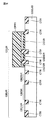
まず、図2に示すように、SOI基板SUBが準備される。SOI基板SUBでは、たとえば、シリコン基板SSUBの上に、埋め込み酸化膜BOLを介在させてシリコン層SLが形成されている。次に、所定の写真製版処理とエッチング処理を施すことにより、分離領域を形成するためのトレンチ分離溝TRE(図4参照)が形成される。次に、そのトレンチ分離溝TREを埋め込むように、SOI基板SUBの上にシリコン酸化膜等の絶縁膜(図示せず)が形成される。 First, as shown in FIG. 2, an SOI substrate SUB is prepared. In the SOI substrate SUB, for example, a silicon layer SL is formed on the silicon substrate SSUB with a buried oxide film BOL interposed. Next, by performing a predetermined photoengraving process and etching process, a trench isolation groove TRE (see FIG. 4) for forming an isolation region is formed. Next, an insulating film (not shown) such as a silicon oxide film is formed on the SOI substrate SUB so as to fill the trench isolation trench TRE.
次に、たとえば、化学的機械研磨処理を施して、SOI基板SUBの上面上に位置する絶縁膜の部分を除去することにより、図3および図4に示すように、トレンチ分離溝TRE内に位置する絶縁膜の部分がトレンチ分離絶縁膜TLとして残されて、分離領域TRが形成される。分離領域TRによって、素子形成領域SR(活性領域)が規定される。後述するように、素子形成領域SRには、バルク用トランジスタやSOI用トランジスタ等の所定の半導体素子が形成される素子形成領域と、ダミー素子形成領域とが含まれる。 Next, for example, a chemical mechanical polishing process is performed to remove a portion of the insulating film located on the upper surface of the SOI substrate SUB, so that a position in the trench isolation trench TRE is obtained as shown in FIGS. A portion of the insulating film to be left is left as the trench isolation insulating film TL, and the isolation region TR is formed. The isolation region TR defines an element formation region SR (active region). As will be described later, the element formation region SR includes an element formation region where a predetermined semiconductor element such as a bulk transistor or an SOI transistor is formed, and a dummy element formation region.
ここで、素子形成領域SR(分離領域TR)のパターンとして、SOI領域とバルク領域との境界に、素子形成領域が配置されないパターンが設定(規定)される。このパターンの作成手法については、最後の実施の形態において説明する。 Here, as a pattern of the element formation region SR (isolation region TR), a pattern in which the element formation region is not disposed is set (defined) at the boundary between the SOI region and the bulk region. This pattern creation method will be described in the last embodiment.
次に、SOI領域とバルク領域とが形成される。図5および図6に示すように、所定の写真製版処理を施すことにより、SOI領域が配置されることになる領域に、フォトレジストPR1が形成される。次に、そのフォトレジストPR1をエッチングマスクとして、露出した、SOI基板SUBの領域にエッチング処理を施すことにより、シリコン層SLおよび埋め込み酸化膜BOLが除去されて、シリコン基板SSUBの表面が露出したバルク領域BURが形成される。 Next, an SOI region and a bulk region are formed. As shown in FIGS. 5 and 6, by performing a predetermined photoengraving process, a photoresist PR1 is formed in a region where the SOI region is to be disposed. Next, by using the photoresist PR1 as an etching mask, the exposed region of the SOI substrate SUB is etched to remove the silicon layer SL and the buried oxide film BOL, thereby exposing the surface of the silicon substrate SSUB. Region BUR is formed.
バルク領域BURでは、残された分離領域TRによって、バルク用トランジスタ等の半導体素子が形成されることになる素子形成領域BSRと、ダミー素子形成領域BDSRとが規定される。一方、エッチングされずに残されたSOI基板SUBの部分がSOI領域SLRとなる。SOI領域SLRでは、分離領域TRによって、SOI用トランジスタ等の半導体素子が形成されることになる素子形成領域SSRと、ダミー素子形成領域SDSRとが規定される。その後、フォトレジストPR1が除去される。 In the bulk region BUR, the remaining isolation region TR defines an element formation region BSR where a semiconductor element such as a bulk transistor is to be formed and a dummy element formation region BDSR. On the other hand, the portion of the SOI substrate SUB that remains without being etched becomes the SOI region SLR. In the SOI region SLR, an isolation region TR defines an element formation region SSR in which a semiconductor element such as an SOI transistor is formed and a dummy element formation region SDSR. Thereafter, the photoresist PR1 is removed.
次に、ゲート電極(ゲート配線)が形成される。ゲート電極には、SOI用トランジスタおよびバルク用トランジスタのそれぞれのゲート電極と、ダミーゲート電極とが含まれる。ゲート電極のパターンとして、SOI領域とバルク領域との境界に、ゲート電極が配置されないパターンが設定(規定)される。このパターンの作成手法については、最後の実施の形態において説明する。 Next, a gate electrode (gate wiring) is formed. The gate electrode includes each gate electrode of the SOI transistor and the bulk transistor, and a dummy gate electrode. As a pattern of the gate electrode, a pattern in which the gate electrode is not disposed is set (defined) at the boundary between the SOI region and the bulk region. This pattern creation method will be described in the last embodiment.
図7および図8に示すように、熱酸化処理を施すことにより、シリコン酸化膜SOLが形成される。シリコン酸化膜SOLを覆うように、たとえば、化学的気相成長法により、ポリシリコン膜POLが形成される。ポリシリコン膜POLを覆うように、シリコン窒化膜SNが形成される。所定の写真製版処理を施すことにより、ゲート電極をパターニングするためのフォトレジストPR2が形成される。 As shown in FIGS. 7 and 8, a silicon oxide film SOL is formed by performing a thermal oxidation process. A polysilicon film POL is formed by, for example, chemical vapor deposition so as to cover silicon oxide film SOL. A silicon nitride film SN is formed so as to cover the polysilicon film POL. By performing a predetermined photolithography process, a photoresist PR2 for patterning the gate electrode is formed.
次に、フォトレジストPR2をエッチングマスクとして、露出したシリコン窒化膜SNにエッチング処理を施すことによって、ゲート電極をパターニングするためのハードマスクが形成される。そのハードマスク等をエッチングマスクとしてエッチング処理を施すことにより、ゲート電極が形成される。その後、フォトレジストPR2が除去される。 Next, a hard mask for patterning the gate electrode is formed by etching the exposed silicon nitride film SN using the photoresist PR2 as an etching mask. By performing an etching process using the hard mask or the like as an etching mask, a gate electrode is formed. Thereafter, the photoresist PR2 is removed.
これにより、図9および図10に示すように、SOI領域SLRでは、ゲート電極SGEとダミーゲート電極SDGEが形成される。SOI用トランジスタのゲート電極SGEは、素子形成領域SSRを横切るように配置されている。バルク領域BURでは、ゲート電極BGEとダミーゲート電極BDGEが形成される。バルク用トランジスタのゲート電極BGEは、素子形成領域BSRを横切るように配置されている。 As a result, as shown in FIGS. 9 and 10, in the SOI region SLR, the gate electrode SGE and the dummy gate electrode SDGE are formed. The gate electrode SGE of the SOI transistor is disposed so as to cross the element formation region SSR. In the bulk region BUR, the gate electrode BGE and the dummy gate electrode BDGE are formed. The gate electrode BGE of the bulk transistor is disposed so as to cross the element formation region BSR.
次に、バルク用トランジスタのエクステンション注入が行われる。ここでは、図面に示されるバルク用トランジスタとしては、nチャネル型のバルク用トランジスタを想定して説明する。 Next, extension implantation of the bulk transistor is performed. Here, as a bulk transistor shown in the drawings, an n-channel bulk transistor is assumed.
図11および図12に示すように、所定の写真製版処理を施すことにより、SOI領域の全体を覆うフォトレジストPR3が形成される。そのフォトレジストPR3のパターンの作成方法については、最後の実施の形態において説明する。なお、フォトレジストPR3は、SOI領域SLRの他に、pチャネル型のバルク用トランジスタ(図示せず)が形成される領域も覆うように形成されている。 As shown in FIGS. 11 and 12, by performing a predetermined photoengraving process, a photoresist PR3 that covers the entire SOI region is formed. A method for creating the pattern of the photoresist PR3 will be described in the last embodiment. Note that the photoresist PR3 is formed so as to cover a region where a p-channel bulk transistor (not shown) is formed in addition to the SOI region SLR.
次に、図13に示すように、フォトレジストPR3等を注入マスクとして、n型領域へ不純物を注入することにより、素子形成領域BSRにエクステンション領域BETが形成される。n型領域への不純物の例として、窒素(N2)、ヒ素(As)およびリン(P)等がある。特に、窒素(N2)の場合、そのドーピング濃度は、1×1020cm-3程度とされる。このとき、n型の不純物は、バルク領域BURのダミー素子形成領域BDSRにも注入されることになる。その後、フォトレジストPR3が除去される。 Next, as shown in FIG. 13, an extension region BET is formed in the element formation region BSR by implanting impurities into the n-type region using the photoresist PR3 or the like as an implantation mask. Examples of impurities in the n-type region include nitrogen (N 2 ), arsenic (As), and phosphorus (P). In particular, in the case of nitrogen (N 2 ), the doping concentration is about 1 × 10 20 cm −3 . At this time, the n-type impurity is also implanted into the dummy element formation region BDSR of the bulk region BUR. Thereafter, the photoresist PR3 is removed.
次に、pチャネル型のバルク用トランジスタ(図示せず)のエクステンション注入が行われる。SOI領域を覆うとともに、nチャネル型のバルク用トランジスタが形成される領域を覆うフォトレジスト(図示せず)等を注入マスクとして、たとえば、フッ化ボロン(BF2)を注入することによりエクステンション領域(図示せず)が形成される。 Next, extension implantation of a p-channel bulk transistor (not shown) is performed. An extension region (for example, boron fluoride (BF 2 ) is implanted by using, as an implantation mask, a photoresist (not shown) that covers the region where the n-channel bulk transistor is formed and covers the SOI region. (Not shown) is formed.
次に、SOI領域SLRにおける所定の領域にせり上げエピタキシャル層を形成する際に、所定の領域以外の領域にエピタキシャル層が形成されるのを阻止する膜(保護膜)が形成される。図14に示すように、ゲート電極SGE、BGEおよびダミーゲート電極SDGE、BDGEを覆うように、たとえば、シリコン窒化膜ESLが形成される。 Next, when the raised epitaxial layer is formed in a predetermined region in the SOI region SLR, a film (protective film) that prevents the epitaxial layer from being formed in a region other than the predetermined region is formed. As shown in FIG. 14, for example, a silicon nitride film ESL is formed so as to cover the gate electrodes SGE, BGE and the dummy gate electrodes SDGE, BDGE.
次に、図15および図16に示すように、所定の写真製版処理を施すことにより、SOI領域SLRを露出し、バルク領域BUR等を覆うフォトレジストPR4が形成される。次に、フォトレジストPR4をエッチングマスクとして、露出しているシリコン窒化膜ESLに異方性のエッチング処理を施すことにより、せり上げエピタキシャル層が形成される素子形成領域SSR等に位置するシリコン層SLの部分が露出する。 Next, as shown in FIGS. 15 and 16, a predetermined photoengraving process is performed to form a photoresist PR4 that exposes the SOI region SLR and covers the bulk region BUR and the like. Next, an anisotropic etching process is performed on the exposed silicon nitride film ESL using the photoresist PR4 as an etching mask, so that the silicon layer SL located in the element formation region SSR or the like where the raised epitaxial layer is formed. Is exposed.
このとき、ゲート電極SGE等の側壁には、シリコン窒化膜ESLが側壁保護膜ESLSとして残される。その後、フォトレジストPR4が除去される。次に、図17に示すように、エピタキシャル成長法によって、露出した素子形成領域SSRにせり上げエピタキシャル層EELが形成される。 At this time, the silicon nitride film ESL is left as the side wall protective film ESLS on the side walls of the gate electrode SGE and the like. Thereafter, the photoresist PR4 is removed. Next, as shown in FIG. 17, a raised epitaxial layer EEL is formed in the exposed element formation region SSR by an epitaxial growth method.
次に、図18に示すように、所定の写真製版処理を施すことにより、SOI領域SLRを覆いバルク領域BURを露出するフォトレジストPR5が形成される。次に、フォトレジストPR5をエッチングマスクとして、露出しているシリコン窒化膜ESLに異方性エッチングを施すことにより、素子形成領域BSR等に位置するシリコン基板SSUBの表面が露出する。また、ゲート電極BGE等の側壁に側壁保護膜ESLBが形成される。その後、フォトレジストPR5が除去される。 Next, as shown in FIG. 18, a predetermined photoengraving process is performed to form a photoresist PR5 that covers the SOI region SLR and exposes the bulk region BUR. Next, anisotropic etching is performed on the exposed silicon nitride film ESL using the photoresist PR5 as an etching mask, thereby exposing the surface of the silicon substrate SSUB located in the element formation region BSR and the like. Further, a sidewall protective film ESLB is formed on the sidewall of the gate electrode BGE and the like. Thereafter, the photoresist PR5 is removed.
次に、図19に示すように、所定のウェットエッチング処理を施すことにより、側壁保護膜ESLS、ESLB等が除去される。このとき、ゲート電極SGE等の側壁に側壁保護膜ESLSが残されているSOI領域SLRの状態と同様に、バルク領域BURでは、ゲート電極BGE等の側壁に側壁保護膜ESLBが残されている状態となっている。これにより、バルク領域BURの全体がシリコン窒化膜ESLによって覆われている場合と比較して、SOI領域SLRに過度のエッチングが施されることによるダメージを抑制することができる。 Next, as shown in FIG. 19, the sidewall protective films ESLS, ESLB and the like are removed by performing a predetermined wet etching process. At this time, in the bulk region BUR, the side wall protective film ESLB is left on the side wall of the gate electrode BGE and the like, similarly to the state of the SOI region SLR in which the side wall protective film ESLS is left on the side wall of the gate electrode SGE and the like. It has become. Thereby, compared with the case where the entire bulk region BUR is covered with the silicon nitride film ESL, damage caused by excessive etching on the SOI region SLR can be suppressed.
次に、SOI用トランジスタのエクステンション注入が行われる。ここでは、図面に示されるSOI用トランジスタとしては、nチャネル型のSOI用トランジスタを想定して説明する。図20および図21に示すように、所定の写真製版処理を施すことにより、SOI領域SLRを露出し、バルク領域BURを覆うフォトレジストPR6が形成される。 Next, extension implantation of the SOI transistor is performed. Here, as an SOI transistor shown in the drawing, an n-channel SOI transistor is assumed. As shown in FIGS. 20 and 21, by performing a predetermined photoengraving process, a photoresist PR6 exposing SOI region SLR and covering bulk region BUR is formed.
次に、フォトレジストPR6を注入マスクとして、たとえば、ヒ素(As)等のn型の不純物を注入することにより、素子形成領域SSRに、エクステンション領域SETが形成される。このとき、n型の不純物は、SOI領域SLRのダミー素子形成領域SDSRにも注入される。その後、フォトレジストPR6が除去される。 Next, an extension region SET is formed in the element formation region SSR by implanting an n-type impurity such as arsenic (As) using the photoresist PR6 as an implantation mask. At this time, the n-type impurity is also implanted into the dummy element formation region SDSR of the SOI region SLR. Thereafter, the photoresist PR6 is removed.
次に、pチャネル型のSOI用トランジスタ(図示せず)のエクステンション注入が行われる。バルク領域を覆うとともに、nチャネル型のSOI用トランジスタが形成される領域を覆うフォトレジスト(図示せず)を注入マスクとして、たとえば、フッ化ボロン(BF2)を注入することによりエクステンション領域(図示せず)が形成される。 Next, extension implantation of a p-channel SOI transistor (not shown) is performed. For example, boron fluoride (BF 2 ) is implanted into the extension region (FIG. 5) using a photoresist (not shown) covering the bulk region and the region where the n-channel SOI transistor is formed as an implantation mask. Not shown).
次に、ゲート電極SGE、BGE等の側壁にサイドウォール膜が形成される。図22に示すように、ゲート電極SGE、BGEおよびダミーゲート電極SDGE、BDGE等を覆うように、シリコン窒化膜SNSDが形成される。 Next, sidewall films are formed on the sidewalls of the gate electrodes SGE, BGE and the like. As shown in FIG. 22, a silicon nitride film SNSD is formed so as to cover gate electrodes SGE, BGE, dummy gate electrodes SDGE, BDGE, and the like.
次に、図23に示すように、シリコン窒化膜SNSDの全面に異方性エッチングを施すことにより、SOI領域SLRでは、ゲート電極SGEおよびダミーゲート電極SDGEのそれぞれの側壁にサイドウォール膜SSWが形成される。バルク領域BURでは、ゲート電極BGEおよびダミーゲート電極BDGEのそれぞれの側壁にサイドウォール膜BSWが形成される。 Next, as shown in FIG. 23, by performing anisotropic etching on the entire surface of the silicon nitride film SNSD, sidewall films SSW are formed on the sidewalls of the gate electrode SGE and the dummy gate electrode SDGE in the SOI region SLR. Is done. In the bulk region BUR, sidewall films BSW are formed on the side walls of the gate electrode BGE and the dummy gate electrode BDGE.
次に、nチャネル型のSOI用トランジスタおよびバルク用トランジスタのそれぞれのソース・ドレイン注入が行われる。pチャネル型のSOI用トランジスタおよびバルク用トランジスタがそれぞれ形成される領域を覆い、nチャネル型のSOI用トランジスタおよびバルク用トランジスタがそれぞれ形成される領域を露出するフォトレジスト(図示せず)が形成される。 Next, source / drain implantation of each of the n-channel type SOI transistor and the bulk transistor is performed. A photoresist (not shown) is formed to cover the regions where the p-channel SOI transistor and the bulk transistor are formed, and to expose the regions where the n-channel SOI transistor and the bulk transistor are formed. The
次に、図24に示すように、露出した領域に、n型の不純物として、たとえば、ヒ素(AS)およびリン(P)を注入することにより、SOI領域SLRでは、ソース・ドレイン領域SSDが形成される。バルク領域BURでは、ソース・ドレイン領域BSDが形成される。こうして、SOI領域SLRにSOI用トランジスタSTRが形成され、バルク領域BURにバルク用トランジスタBTRが形成される。 Next, as shown in FIG. 24, for example, arsenic (AS) and phosphorus (P) are implanted into the exposed region as n-type impurities, thereby forming source / drain regions SSD in the SOI region SLR. Is done. In the bulk region BUR, a source / drain region BSD is formed. Thus, the SOI transistor STR is formed in the SOI region SLR, and the bulk transistor BTR is formed in the bulk region BUR.
次に、pチャネル型のSOI用トランジスタおよびバルク用トランジスタのそれぞれのソース・ドレイン注入が行われる。pチャネル型のSOI用トランジスタおよびバルク用トランジスタがそれぞれ形成される領域を露出し、nチャネル型のSOI用トランジスタおよびバルク用トランジスタがそれぞれ形成される領域を覆うフォトレジスト(図示せず)を注入マスクとして、p型の不純物として、たとえば、ボロン(B)を注入することによりソース・ドレイン領域(図示せず)が形成される。 Next, source / drain implantation of each of the p-channel SOI transistor and the bulk transistor is performed. A region where the p-channel SOI transistor and the bulk transistor are formed is exposed, and a photoresist (not shown) covering the region where the n-channel SOI transistor and the bulk transistor are formed is implanted. As a p-type impurity, for example, boron (B) is implanted to form a source / drain region (not shown).
次に、サリサイド(Self ALIgned siliCIDE)法により、金属シリサイド膜が形成される。ゲート電極SGE、BGE、ダミーゲート電極SDGE、BDGEおよびソース・ドレイン領域SSD、BSD等を覆うように、たとえば、コバルト膜等の金属膜(図示せず)が形成される。次に、所定の温度のもとで熱処理が施される。 Next, a metal silicide film is formed by a salicide (Self ALIgned siliCIDE) method. For example, a metal film (not shown) such as a cobalt film is formed so as to cover the gate electrodes SGE and BGE, the dummy gate electrodes SDGE and BDGE, and the source / drain regions SSD and BSD. Next, heat treatment is performed under a predetermined temperature.
これにより、ゲート電極SGE、BGE、ダミーゲート電極SDGE、BDGE中のシリコンと金属とが反応することで、金属シリサイド膜が形成される。また、ソース・ドレイン領域SSD、BSD中のシリコンと金属とが反応することで、金属シリサイド膜が形成される。その後、未反応の金属膜を除去することで、図25に示すように、金属シリサイド膜MSが露出する。 As a result, the metal in the gate electrodes SGE, BGE, dummy gate electrodes SDGE, BDGE reacts with the metal to form a metal silicide film. Further, the metal in the source / drain regions SSD and BSD reacts with the metal to form a metal silicide film. Thereafter, the unreacted metal film is removed to expose the metal silicide film MS as shown in FIG.
次に、図26に示すように、SOI用トランジスタおよびバルク用トランジスタ等を覆うように、ストレスライナー膜としてシリコン窒化膜SNLが形成される。次に、シリコン窒化膜SNLを覆うように、所定の厚さを有する、たとえば、シリコン酸化膜等のコンタクト層間絶縁膜CILが形成される。 Next, as shown in FIG. 26, a silicon nitride film SNL is formed as a stress liner film so as to cover the SOI transistor, the bulk transistor, and the like. Next, a contact interlayer insulating film CIL such as a silicon oxide film having a predetermined thickness is formed so as to cover silicon nitride film SNL.
次に、コンタクト層間絶縁膜CILに所定の写真製版処理およびエッチング処理を施すことにより、金属シリサイド膜MSを露出するコンタクトホールが形成される。次に、コンタクトホールの側壁面を含むコンタクト層間絶縁膜CILの表面上にバリアメタルとなる、たとえば、チタン(Ti)膜を介在させてタングステン(W)膜(いずれも図示せず)が形成される。次に、化学的機械研磨処理を施すことにより、コンタクト層間絶縁膜CILの上面上に位置するタングステン膜の部分およびチタン膜の部分が除去される。 Next, the contact interlayer insulating film CIL is subjected to a predetermined photolithography process and an etching process, thereby forming a contact hole exposing the metal silicide film MS. Next, a tungsten (W) film (not shown) is formed on the surface of the contact interlayer insulating film CIL including the sidewall surface of the contact hole, for example, with a titanium (Ti) film interposed therebetween. The Next, by performing chemical mechanical polishing, the tungsten film portion and the titanium film portion located on the upper surface of the contact interlayer insulating film CIL are removed.
これにより、図27に示すように、SOI領域SLRでは、コンタクトホールCH内にコンタクトプラグPLSが形成される。バルク領域BURでは、コンタクトホールCH内にコンタクトプラグPLBが形成される。次に、図28に示すように、コンタクト層間絶縁膜CILを覆うように、配線層間絶縁膜WIL1が形成される。その配線層間絶縁膜WIL1を覆うように、さらに、配線層間絶縁膜WIL2が形成される。 Thereby, as shown in FIG. 27, in the SOI region SLR, a contact plug PLS is formed in the contact hole CH. In the bulk region BUR, a contact plug PLB is formed in the contact hole CH. Next, as shown in FIG. 28, a wiring interlayer insulating film WIL1 is formed so as to cover the contact interlayer insulating film CIL. A wiring interlayer insulating film WIL2 is further formed so as to cover the wiring interlayer insulating film WIL1.
次に、図29に示すように、配線層間絶縁膜WIL2および配線層間絶縁膜WIL1に所定の写真製版処理およびエッチング処理を施すことにより、SOI領域SLRでは、コンタクトプラグPLSを露出する配線溝WTRが形成される。バルク領域BURでは、コンタクトプラグPLBを露出する配線溝WTRが形成される。 Next, as shown in FIG. 29, a predetermined photoengraving process and an etching process are performed on the wiring interlayer insulating film WIL2 and the wiring interlayer insulating film WIL1, thereby forming a wiring groove WTR that exposes the contact plug PLS in the SOI region SLR. It is formed. In the bulk region BUR, a wiring trench WTR that exposes the contact plug PLB is formed.
次に、配線溝WTRの底面および側壁面を含む配線層間絶縁膜WIL2の表面上にバリアメタルとなる、たとえば、タンタル(Ta)膜を介在させて銅(Cu)膜(いずれも図示せず)が形成される。次に、化学的機械研磨処理を施すことにより、配線層間絶縁膜WIL2の上面上に位置する銅膜の部分およびタンタル膜の部分が除去される。 Next, for example, a copper (Cu) film (not shown) with a tantalum (Ta) film interposed as a barrier metal on the surface of the wiring interlayer insulating film WIL2 including the bottom surface and the side wall surface of the wiring trench WTR. Is formed. Next, by performing a chemical mechanical polishing treatment, the copper film portion and the tantalum film portion located on the upper surface of the wiring interlayer insulating film WIL2 are removed.
これにより、図30に示すように、SOI領域SLRでは、配線溝WTRに配線WISが形成される。バルク領域BURでは、配線溝WTRに配線WIBが形成される。配線WISは、コンタクトプラグPLSおよび金属シリサイド膜MSを介して、SOI用トランジスタのソース・ドレイン領域SSDに電気的に接続される。配線WIBは、コンタクトプラグPLBおよび金属シリサイド膜MSを介して、バルク用トランジスタのソース・ドレイン領域BSDに電気的に接続される。 Thereby, as shown in FIG. 30, in the SOI region SLR, the wiring WIS is formed in the wiring trench WTR. In the bulk region BUR, the wiring WIB is formed in the wiring trench WTR. The wiring WIS is electrically connected to the source / drain region SSD of the SOI transistor via the contact plug PLS and the metal silicide film MS. The wiring WIB is electrically connected to the source / drain region BSD of the bulk transistor through the contact plug PLB and the metal silicide film MS.
その後、必要に応じて、上層の層間絶縁膜と配線(いずれも図示せず)が形成される。こうして、SOI用トランジスタおよびバルク用トランジスタ等を備えた半導体装置の主要部分が完成する。 Thereafter, if necessary, an upper interlayer insulating film and wiring (both not shown) are formed. Thus, the main part of the semiconductor device including the SOI transistor and the bulk transistor is completed.
上述した半導体装置では、SOI領域SLRとバルク領域BURとの段差の側壁に、全周にわたって分離領域TR(トレンチ分離絶縁膜TL)を露出させることで、せり上げエピタキシャル層EELを形成する際に、SOI領域SLRにおいてエピタキシャル層が異常成長するのを抑制することができる。また、バルク領域BURへのエクステンション注入を行う際に、SOI領域SLRを覆うフォトレジストPR3を形成することで、SOI領域SLRにおいてエピタキシャル層が異常成長するのを抑制することができる。このことについて、比較例に係る半導体装置と比較しながら説明する。 In the semiconductor device described above, when the raised epitaxial layer EEL is formed by exposing the isolation region TR (trench isolation insulating film TL) over the entire circumference on the side wall of the step between the SOI region SLR and the bulk region BUR, Abnormal growth of the epitaxial layer in the SOI region SLR can be suppressed. In addition, when the extension implantation into the bulk region BUR is performed, the formation of the photoresist PR3 covering the SOI region SLR can suppress the abnormal growth of the epitaxial layer in the SOI region SLR. This will be described in comparison with a semiconductor device according to a comparative example.
準備されたSOI基板CSUBに対して、所定の写真製版処理とエッチング処理を施すことにより、分離領域を形成するためのトレンチ分離溝CTRE(図32参照)が形成される。次に、そのトレンチ分離溝CTREを埋め込むように、SOI基板CSUBの上にシリコン酸化膜等の絶縁膜(図示せず)が形成される。 A trench isolation groove CTRE (see FIG. 32) for forming an isolation region is formed by subjecting the prepared SOI substrate CSUB to predetermined photolithography and etching. Next, an insulating film (not shown) such as a silicon oxide film is formed on the SOI substrate CSUB so as to fill the trench isolation trench CTRE.
次に、化学的機械研磨処理を施して、SOI基板CSUBの上面上に位置する絶縁膜の部分を除去することにより、図31および図32に示すように、トレンチ分離溝CTRE内に残されたトレンチ分離絶縁膜CTLによって分離領域CTRが形成される。分離領域CTRによって、素子形成領域CSRが規定される。 Next, a chemical mechanical polishing process is performed to remove a portion of the insulating film located on the upper surface of the SOI substrate CSUB, thereby leaving the trench isolation trench CTRE as shown in FIGS. An isolation region CTR is formed by the trench isolation insulating film CTL. The element formation region CSR is defined by the isolation region CTR.
比較例に係る半導体装置の素子形成領域CSR(分離領域CTR)では、SOI領域とバルク領域との境界について考慮されておらず、素子形成領域CSRのパターンとしては、素子形成領域CSRが境界に跨るように位置するパターンが存在する。 In the element formation region CSR (isolation region CTR) of the semiconductor device according to the comparative example, the boundary between the SOI region and the bulk region is not considered, and the element formation region CSR straddles the boundary as the pattern of the element formation region CSR. There is a pattern located as follows.
次に、図33および図34に示すように、所定の写真製版処理を施すことにより、SOI領域が配置されることになる領域に、フォトレジストCPR1が形成される。次に、そのフォトレジストCPR1をエッチングマスクとして、露出したSOI基板CSUBの領域にエッチング処理を施すことにより、シリコン基板CSSUBの表面が露出したバルク領域CBURが形成される。 Next, as shown in FIGS. 33 and 34, by performing a predetermined photoengraving process, a photoresist CPR1 is formed in the region where the SOI region is to be disposed. Next, using the photoresist CPR1 as an etching mask, the exposed region of the SOI substrate CSUB is subjected to an etching process, thereby forming a bulk region CBUR where the surface of the silicon substrate CSSUB is exposed.
バルク領域CBURでは、残された分離領域CTRによって、素子形成領域CBSRとダミー素子形成領域CBDSRとが規定される。一方、エッチングされずに残されたSOI基板CSUBの部分がSOI領域CSLRとなる。SOI領域CSLRでは、分離領域CTRによって、素子形成領域CSSRとダミー素子形成領域CSDSRとが規定される。その後、フォトレジストCPR1が除去される。 In the bulk region CBUR, an element formation region CBSR and a dummy element formation region CBDSR are defined by the remaining isolation region CTR. On the other hand, the portion of the SOI substrate CSUB that remains without being etched becomes the SOI region CSLR. In the SOI region CSLR, the element formation region CSSR and the dummy element formation region CSDSR are defined by the isolation region CTR. Thereafter, the photoresist CPR1 is removed.
次に、ゲート電極(ゲート配線)が形成される。図35および図36に示すように、ゲート酸化膜となるシリコン酸化膜CSOLが形成される。シリコン酸化膜CSOLを覆うように、ポリシリコン膜CPOLが形成される。ポリシリコン膜CPOLを覆うように、シリコン窒化膜CSNが形成される。所定の写真製版処理を施すことにより、ゲート電極をパターニングするためのフォトレジストCPR2が形成される。比較例に係る半導体装置のゲート電極(ゲート配線)のパターンとしては、ゲート電極が境界に跨るように位置するパターンが存在する。 Next, a gate electrode (gate wiring) is formed. As shown in FIGS. 35 and 36, a silicon oxide film CSOL to be a gate oxide film is formed. A polysilicon film CPOL is formed so as to cover the silicon oxide film CSOL. A silicon nitride film CSN is formed so as to cover the polysilicon film CPOL. By performing a predetermined photolithography process, a photoresist CPR2 for patterning the gate electrode is formed. As a pattern of the gate electrode (gate wiring) of the semiconductor device according to the comparative example, there is a pattern positioned so that the gate electrode straddles the boundary.
次に、フォトレジストCPR2等をエッチングマスクとして、エッチング処理を施すことによってゲート電極が形成される。その後、フォトレジストCPR2が除去される。これにより、図37および図38に示すように、SOI領域CSLRでは、ゲート電極CSGEとダミーゲート電極CSDGEが形成される。バルク領域CBURでは、ゲート電極CBGEとダミーゲート電極CBDGEが形成される。ダミーゲート電極には、SOI領域CSLRとバルク領域CBURとの境界に跨るダミーゲート電極が存在する。 Next, a gate electrode is formed by performing an etching process using the photoresist CPR2 or the like as an etching mask. Thereafter, the photoresist CPR2 is removed. Thereby, as shown in FIGS. 37 and 38, the gate electrode CSGE and the dummy gate electrode CSDGE are formed in the SOI region CSLR. In the bulk region CBUR, a gate electrode CBGE and a dummy gate electrode CBDGE are formed. The dummy gate electrode includes a dummy gate electrode straddling the boundary between the SOI region CSLR and the bulk region CBUR.
次に、バルク用トランジスタのエクステンション注入が行われる。ここでは、図面に示されるバルク用トランジスタとしては、nチャネル型のバルク用トランジスタを想定して説明する。 Next, extension implantation of the bulk transistor is performed. Here, as a bulk transistor shown in the drawings, an n-channel bulk transistor is assumed.
図39および図40に示すように、所定の写真製版処理を施すことにより、SOI領域CSLRにおける、素子形成領域CSSRを覆うフォトレジストCPR3が形成される。なお、フォトレジストCPR3は、pチャネル型のバルク用トランジスタ(図示せず)が形成される領域も覆っている。 As shown in FIGS. 39 and 40, by applying a predetermined photoengraving process, in the SOI region CSLR, photoresist CPR3 is formed to cover the element formation region CSS R. Note that the photoresist CPR3 also covers a region where a p-channel bulk transistor (not shown) is formed.
次に、図41に示すように、フォトレジストCPR3を注入マスクとして、n型領域へ不純物を注入することにより、素子形成領域CBSRにエクステンション領域CBETが形成される。このとき、n型領域への不純物は、バルク領域CBURのダミー素子形成領域CBDSRにも注入されることになる。その後、フォトレジストCPR3が除去される。 Next, as shown in FIG. 41, an extension region CBET is formed in the element formation region CBSR by implanting impurities into the n-type region using the photoresist CPR3 as an implantation mask. At this time, impurities to the n-type region are also implanted into the dummy element formation region CBDSR of the bulk region CBUR. Thereafter, the photoresist CPR3 is removed.
次に、pチャネル型のバルク用トランジスタ(図示せず)のエクステンション注入が行われた後、所定の領域以外の領域にエピタキシャル層が形成されるのを阻止する膜が形成される。ゲート電極CSGE、CBGEおよびダミーゲート電極CSDGE、CBDGEを覆うように、シリコン窒化膜CESL(図43参照)が形成される。 Next, after extension implantation of a p-channel bulk transistor (not shown) is performed, a film for preventing the formation of an epitaxial layer in a region other than a predetermined region is formed. A silicon nitride film CESL (see FIG. 43) is formed so as to cover gate electrodes CSGE and CBGE and dummy gate electrodes CSDGE and CBDGE.
次に、図42および図43に示すように、所定の写真製版処理を施すことにより、SOI領域CSLRを露出し、バルク領域CBUR等を覆うフォトレジストCPR4が形成される。次に、フォトレジストCPR4をエッチングマスクとして、露出しているシリコン窒化膜CESLに異方性のエッチング処理を施すことにより、せり上げエピタキシャル層が形成される素子形成領域CSSR等に位置するシリコン層CSLの部分が露出する。また、ゲート電極CSGE等の側壁には、シリコン窒化膜CESLが側壁保護膜CESLSとして残される。その後、フォトレジストCPR4が除去される。 Next, as shown in FIGS. 42 and 43, by performing a predetermined photoengraving process, a photoresist CPR4 that exposes the SOI region CSLR and covers the bulk region CBUR and the like is formed. Next, by using the photoresist CPR4 as an etching mask, the exposed silicon nitride film CESL is subjected to anisotropic etching to form a silicon layer CSL located in an element formation region CSSR or the like where a raised epitaxial layer is formed. Is exposed. Further, the silicon nitride film CESL is left as the sidewall protective film CESLS on the side walls of the gate electrode CSGE and the like. Thereafter, the photoresist CPR4 is removed.
次に、図44に示すように、エピタキシャル成長法によって、露出した素子形成領域CSSRにせり上げエピタキシャル層CEELが形成される。その後、SOI用トランジスタのエクステンション領域、SOI用トランジスタおよびバルク用トランジスタのそれぞれのソース・ドレイン領域、コンタクトプラグおよび配線等(いずれも図示せず)が形成されて、比較例に係る半導体装置の主要部分が完成する。 Next, as shown in FIG. 44, an epitaxial layer CEEL is formed in the exposed element formation region CSSR by an epitaxial growth method. Thereafter, the extension region of the SOI transistor, the source / drain regions of each of the SOI transistor and the bulk transistor, contact plugs, wirings, etc. (all not shown) are formed, and the main part of the semiconductor device according to the comparative example Is completed.
比較例に係る半導体装置では、図45の丸印Aに示すように、ダミー素子形成領域CSDSRのパターンとして、SOI領域CSLRとバルク領域CBURとの境界にシリコン層が露出するように配置されたパターンが存在する。このため、せり上げエピタキシャル層を形成する際に、SOI領域とバルク領域との境界の段差に露出したシリコン層の部分にエピタキシャル層が異常成長することがある。 In the semiconductor device according to the comparative example, as shown by a circle A in FIG. 45, as a pattern of the dummy element formation region CSDSR, a pattern arranged so that the silicon layer is exposed at the boundary between the SOI region CSLR and the bulk region CBUR. Exists. For this reason, when the raised epitaxial layer is formed, the epitaxial layer may grow abnormally in the portion of the silicon layer exposed at the step at the boundary between the SOI region and the bulk region.
また、図41に示すように、バルク用トランジスタのエクステンション領域を形成する際に、SOI領域CSLRに露出したシリコン層の部分へ不純物が注入されることで、シリコン層がアモルファス化してしまうことがある。このため、せり上げエピタキシャル層を形成する際に、アモルファス化したシリコン層の部分にエピタキシャル層が異常成長することがある。 In addition, as shown in FIG. 41, when forming the extension region of the bulk transistor, the silicon layer may become amorphous by implanting impurities into the portion of the silicon layer exposed to the SOI region CSLR. . For this reason, when the raised epitaxial layer is formed, the epitaxial layer may grow abnormally in the amorphous silicon portion.
比較例に係る半導体装置に対して、実施の形態に係る半導体装置では、SOI領域SLRとバルク領域BURとの段差の側壁に、全周にわたって分離領域TR(トレンチ分離絶縁膜TL)が露出する。これにより、せり上げエピタキシャル層EELを形成する際に、SOI領域SLRにおいてエピタキシャル層が異常成長するのを抑制することができる。 In contrast to the semiconductor device according to the comparative example, in the semiconductor device according to the embodiment, the isolation region TR (trench isolation insulating film TL) is exposed on the entire sidewall of the step between the SOI region SLR and the bulk region BUR. Thereby, when the raised epitaxial layer EEL is formed, abnormal growth of the epitaxial layer in the SOI region SLR can be suppressed.
また、バルク領域BURへのエクステンション注入を行う際に、SOI領域SLRを覆うフォトレジストPR3が形成される。これにより、SOI領域に位置するシリコン層がアモルファス化するのを阻止することができ、SOI領域SLRにおいてエピタキシャル層が異常成長するのを抑制することができる。 Further, when performing extension implantation into the bulk region BUR, a photoresist PR3 covering the SOI region SLR is formed. Thereby, the silicon layer located in the SOI region can be prevented from becoming amorphous, and the epitaxial layer can be prevented from growing abnormally in the SOI region SLR.
さらに、SOI領域SLRとバルク領域BURとの段差の側壁に露出した埋め込み酸化膜が、後の工程においてなくなり、その上に位置するシリコン層の部分が異物として剥離してしまうのを抑制することができる。 Further, the buried oxide film exposed on the side wall of the step between the SOI region SLR and the bulk region BUR disappears in a later step, and the silicon layer portion located thereon is prevented from peeling off as a foreign substance. it can.
実施の形態2
ここでは、SOI領域とバルク領域との段差の側壁に、全周にわたって分離領域の分離絶縁膜を露出させ、そして、SOI領域に配置されるダミー素子形成領域の全体をダミー電極によって覆う手法について説明する。なお、実施の形態1と同一部材については同一符号を付し、必要である場合を除きその説明を繰り返さないこととする。
Here, a method of exposing the isolation insulating film of the isolation region over the entire circumference on the side wall of the step between the SOI region and the bulk region, and covering the entire dummy element formation region arranged in the SOI region with a dummy electrode will be described. To do. The same members as those in the first embodiment are denoted by the same reference numerals, and the description thereof will not be repeated unless necessary.
まず、図2〜図4に示す工程と同様の工程を経て、図46および図47に示すように、SOI基板SUBに、分離領域TRが形成される。分離領域TRによって、素子形成領域SRが規定される。素子形成領域SRには、所定の半導体素子が形成される素子形成領域と、ダミー素子形成領域とが含まれる。 First, through steps similar to those shown in FIGS. 2 to 4, isolation region TR is formed in SOI substrate SUB as shown in FIGS. 46 and 47. The element formation region SR is defined by the isolation region TR. The element formation region SR includes an element formation region in which a predetermined semiconductor element is formed and a dummy element formation region.
次に、図5および図6に示す工程と同様の工程を経て、SOI領域とバルク領域とが形成される。バルク領域BURでは、残された分離領域TRによって、バルク用トランジスタ等が形成されることになる素子形成領域BSRと、ダミー素子形成領域BDSRとが規定される。一方、SOI領域SLRでは、分離領域TRによって、SOI用トランジスタ等が形成されることになる素子形成領域SSRと、ダミー素子形成領域SDSRとが規定される(図5および図6参照)。 Next, an SOI region and a bulk region are formed through steps similar to those shown in FIGS. In the bulk region BUR, the remaining isolation region TR defines an element formation region BSR where a bulk transistor or the like is to be formed and a dummy element formation region BDSR. On the other hand, in SOI region SLR, an isolation region TR defines an element formation region SSR in which an SOI transistor or the like is to be formed, and a dummy element formation region SDSR (see FIGS. 5 and 6).
次に、ゲート電極(ゲート配線)が形成される。図7および図8に示す工程と同様の工程を経て、図48および図49に示すように、シリコン酸化膜SOL、ポリシリコン膜POLおよびシリコン窒化膜SNが順次形成される。次に、所定の写真製版処理を施すことにより、ゲート電極をパターニングするためのフォトレジストPR2が形成される。このとき、SOI領域SLRでは、パターニングされるダミーゲート電極によって、一つのダミー素子形成領域SDSRの全体が覆われるように、フォトレジストPR2が形成される。すなわち、パターニングされるダミーゲート電極(サイズ)がダミー素子形成領域SDSR(サイズ)よりも大きくなるように、フォトレジストPR2が形成される。 Next, a gate electrode (gate wiring) is formed. Through the steps similar to those shown in FIGS. 7 and 8, as shown in FIGS. 48 and 49, silicon oxide film SOL, polysilicon film POL, and silicon nitride film SN are sequentially formed. Next, by performing a predetermined photolithography process, a photoresist PR2 for patterning the gate electrode is formed. At this time, in the SOI region SLR, the photoresist PR2 is formed so that the entire dummy element formation region SDSR is covered with the dummy gate electrode to be patterned. That is, the photoresist PR2 is formed so that the dummy gate electrode (size) to be patterned is larger than the dummy element formation region SDSR (size).
次に、フォトレジストPR2をエッチングマスクとして、露出したシリコン窒化膜SNにエッチング処理を施すことによって、ゲート電極をパターニングするためのハードマスクが形成される。そのハードマスク等をエッチングマスクとしてエッチング処理を施すことにより、ゲート電極が形成される。その後、フォトレジストPR2が除去される。 Next, a hard mask for patterning the gate electrode is formed by etching the exposed silicon nitride film SN using the photoresist PR2 as an etching mask. By performing an etching process using the hard mask or the like as an etching mask, a gate electrode is formed. Thereafter, the photoresist PR2 is removed.
これにより、図50および図51に示すように、SOI領域SLRでは、ゲート電極SGEとダミーゲート電極SDGEが形成される。ゲート電極SGEは、素子形成領域SSRを横切るように配置されている。ダミーゲート電極SDGEのサイズは、ダミー素子形成領域SDSRのサイズよりも大きく、ダミーゲート電極SDGEは、ダミー素子形成領域SDSRの全体を覆うように配置されている。バルク領域BURでは、ゲート電極BGEとダミーゲート電極BDGEが形成される。ゲート電極BGEは、素子形成領域BSRを横切るように配置されている。 Thereby, as shown in FIGS. 50 and 51, the gate electrode SGE and the dummy gate electrode SDGE are formed in the SOI region SLR. The gate electrode SGE is disposed so as to cross the element formation region SSR. The size of the dummy gate electrode SDGE is larger than the size of the dummy element formation region SDSR, and the dummy gate electrode SDGE is disposed so as to cover the entire dummy element formation region SDSR. In the bulk region BUR, the gate electrode BGE and the dummy gate electrode BDGE are formed. The gate electrode BGE is disposed so as to cross the element formation region BSR.
次に、バルク用トランジスタのエクステンション注入が行われる。なお、図面に示されるバルク用トランジスタとしては、nチャネル型のバルク用トランジスタを想定して説明する。図52および図53に示すように、所定の写真製版処理を施すことにより、フォトレジストPR7が形成される。 Next, extension implantation of the bulk transistor is performed. Note that an n-channel bulk transistor is assumed as a bulk transistor shown in the drawings. As shown in FIGS. 52 and 53, a photoresist PR7 is formed by performing a predetermined photoengraving process.
ここで、SOI領域SLRでは、ダミーゲート電極SDGEがダミー素子形成領域SDSRの全体を覆うように配置されていることで、フォトレジストとしては、SOI領域SLRの全体を覆う必要はなく、SOI領域SLRのうち、素子形成領域SSRとその近傍の領域を覆うフォトレジストPR7が形成される。なお、フォトレジストPR7は、この他に、pチャネル型のバルク用トランジスタ(図示せず)が形成される領域も覆うように形成されている。 Here, in the SOI region SLR, since the dummy gate electrode SDGE is disposed so as to cover the entire dummy element formation region SDSR, it is not necessary for the photoresist to cover the entire SOI region SLR, and the SOI region SLR. Among these, a photoresist PR7 is formed to cover the element formation region SSR and the region in the vicinity thereof. In addition, the photoresist PR7 is formed so as to cover a region where a p-channel bulk transistor (not shown) is formed.
次に、図54に示すように、フォトレジストPR7等を注入マスクとして、n型の不純物を注入することにより、素子形成領域BSRにエクステンション領域BETが形成される。前述したように、n型の不純物の例として、窒素(N2)、ヒ素(As)およびリン(P)等がある。特に、窒素(N2)の場合、そのドーピング濃度は、1×1020cm-3程度とされる。その後、フォトレジストPR7が除去される。次に、pチャネル型のバルク用トランジスタ(図示せず)のエクステンション注入が行われる。 Next, as shown in FIG. 54, an extension region BET is formed in the element formation region BSR by implanting n-type impurities using the photoresist PR7 as an implantation mask. As described above, examples of n-type impurities include nitrogen (N 2 ), arsenic (As), and phosphorus (P). In particular, in the case of nitrogen (N 2 ), the doping concentration is about 1 × 10 20 cm −3 . Thereafter, the photoresist PR7 is removed. Next, extension implantation of a p-channel bulk transistor (not shown) is performed.
次に、図14〜図16に示す工程と同様の工程を経て、所定の領域以外の領域にエピタキシャル層が形成されるのを阻止する膜が形成される。図55および図56に示すように、せり上げエピタキシャル層が形成される素子形成領域SSR等に位置するシリコン層SLの部分を露出し、他の領域を覆うシリコン窒化膜ESLが形成される。次に、図57に示すように、エピタキシャル成長法によって、露出した素子形成領域SSRにせり上げエピタキシャル層EELが形成される。 Next, a film that prevents the formation of an epitaxial layer in a region other than the predetermined region is formed through steps similar to those shown in FIGS. As shown in FIGS. 55 and 56, a silicon nitride film ESL that exposes a portion of the silicon layer SL located in the element formation region SSR or the like where the raised epitaxial layer is formed and covers the other region is formed. Next, as shown in FIG. 57, a raised epitaxial layer EEL is formed in the exposed element formation region SSR by an epitaxial growth method.
次に、図18および図19に示す工程と同様の工程を経て、シリコン窒化膜ESLが除去される。次に、図20および図21に示す工程と同様の工程を経て、素子形成領域SSRに、エクステンション領域SETが形成される(図58参照)。次に、図22および図23に示す工程と同様の工程を経て、SOI領域SLRでは、ゲート電極SGEおよびダミーゲート電極SDGEのそれぞれの側壁にサイドウォール膜SSWが形成され、バルク領域BURでは、ゲート電極BGEおよびダミーゲート電極BDGEのそれぞれの側壁にサイドウォール膜BSWが形成される(図58参照)。 Next, silicon nitride film ESL is removed through steps similar to those shown in FIGS. Next, an extension region SET is formed in the element formation region SSR through steps similar to those shown in FIGS. 20 and 21 (see FIG. 58). Next, through steps similar to those shown in FIGS. 22 and 23, sidewall films SSW are formed on the sidewalls of the gate electrode SGE and the dummy gate electrode SDGE in the SOI region SLR, and in the bulk region BUR, Sidewall films BSW are formed on the side walls of the electrode BGE and the dummy gate electrode BDGE (see FIG. 58).
次に、図24に示す工程と同様の工程を経て、SOI領域SLRでは、ソース・ドレイン領域SSDが形成され、バルク領域BURでは、ソース・ドレイン領域BSDが形成される(図58参照)。こうして、SOI領域SLRにSOI用トランジスタSTRが形成され、バルク領域BURにバルク用トランジスタBTRが形成される。次に、図25に示す工程と同様の工程を経て、図58に示すように、金属シリサイド膜MSが形成される。 Next, through a process similar to that shown in FIG. 24, the source / drain region SSD is formed in the SOI region SLR, and the source / drain region BSD is formed in the bulk region BUR (see FIG. 58). Thus, the SOI transistor STR is formed in the SOI region SLR, and the bulk transistor BTR is formed in the bulk region BUR. Next, through a process similar to that shown in FIG. 25, metal silicide film MS is formed as shown in FIG.
次に、図26に示す工程と同様の工程を経て、シリコン窒化膜SNLおよびコンタクト層間絶縁膜CILが形成される(図59参照)。次に、図27に示す工程と同様の工程を経て、コンタクトホールCH内にコンタクトプラグPLS、PLBが形成される(図59参照)。次に、図28に示す工程と同様の工程を経て、配線層間絶縁膜WIL1および配線層間絶縁膜WIL2が形成される(図59参照)。次に、図29に示す工程と同様の工程を経て、配線溝WTRが形成される(図59参照)。 Next, through a process similar to that shown in FIG. 26, silicon nitride film SNL and contact interlayer insulating film CIL are formed (see FIG. 59). Next, through the same process as that shown in FIG. 27, contact plugs PLS and PLB are formed in contact hole CH (see FIG. 59). Next, through a process similar to the process shown in FIG. 28, wiring interlayer insulating film WIL1 and wiring interlayer insulating film WIL2 are formed (see FIG. 59). Next, through a process similar to the process shown in FIG. 29, wiring trench WTR is formed (see FIG. 59).
次に、図30に示す工程と同様の工程を経て、図59に示すように、SOI領域SLRでは配線WISが形成され、バルク領域BURでは配線WIBが形成される。その後、必要に応じて、上層の層間絶縁膜と配線(いずれも図示せず)が形成される。こうして、SOI用トランジスタおよびバルク用トランジスタ等を備えた半導体装置の主要部分が完成する。 Next, steps similar to those shown in FIG. 30 are performed, and as shown in FIG. 59, wiring WIS is formed in SOI region SLR and wiring WIB is formed in bulk region BUR. Thereafter, if necessary, an upper interlayer insulating film and wiring (both not shown) are formed. Thus, the main part of the semiconductor device including the SOI transistor and the bulk transistor is completed.
上述した半導体装置では、SOI領域SLRとバルク領域BURとの段差の側壁に、全周にわたって分離領域TR(トレンチ分離絶縁膜TL)が露出される。これにより、せり上げエピタキシャル層EELを形成する際に、SOI領域SLRにおいてエピタキシャル層が異常成長するのを抑制することができる。 In the semiconductor device described above, the isolation region TR (trench isolation insulating film TL) is exposed over the entire periphery on the side wall of the step between the SOI region SLR and the bulk region BUR. Thereby, when the raised epitaxial layer EEL is formed, abnormal growth of the epitaxial layer in the SOI region SLR can be suppressed.
また、バルク領域BURへのエクステンション注入を行う際に、SOI領域SLRでは、ダミー素子形成領域SDSRの全体がダミーゲート電極SDGEによって覆われ、素子形成領域SSRはフォトレジストPR7によって覆われている。これにより、SOI領域に位置するシリコン層がアモルファス化するのを阻止することができ、せり上げエピタキシャル層を形成する際に、エピタキシャル層が異常成長するのを抑制することができる。 Further, when performing extension implantation into the bulk region BUR, in the SOI region SLR, the entire dummy element formation region SDSR is covered with the dummy gate electrode SDGE, and the element formation region SSR is covered with the photoresist PR7. Thereby, the silicon layer located in the SOI region can be prevented from becoming amorphous, and the epitaxial layer can be prevented from growing abnormally when the raised epitaxial layer is formed.
さらに、エクステンション注入を阻止するフォトレジストとして、フォトレジストPR7を形成することで、SOI領域においてフォトレジストの残渣を抑制することができる。このことについて説明する。エクステンション注入等を行う際に、注入マスクとして形成されるフォトレジストに不純物が注入されると、そのフォトレジストの表面は硬化する。このため、フォトレジストを除去する際に、除去しきれずにフォトレジストが残ることがある。この傾向は、フォトレジストが形成されている領域の面積が増加するにしたがって大きくなる。 Furthermore, by forming a photoresist PR7 as a photoresist that prevents extension implantation, residue of the photoresist can be suppressed in the SOI region. This will be described. When an impurity is implanted into a photoresist formed as an implantation mask during extension implantation or the like, the surface of the photoresist is cured. For this reason, when removing the photoresist, the photoresist may remain without being completely removed. This tendency increases as the area of the region where the photoresist is formed increases.
上述した半導体装置におけるSOI領域SLRでは、ダミーゲート電極SDGEがダミー素子形成領域SDSRの全体を覆うように配置されている。このため、バルク領域へのエクステンション注入の際に形成されるフォトレジストとしては、SOI領域SLRの全体を覆うのではなく、SOI領域SLRのうち、素子形成領域SSRとその近傍の領域を覆うフォトレジストPR7が形成される。これにより、SOI領域SLRにおいて、フォトレジストが形成される領域の面積が削減されて、フォトレジストの残渣を抑制することができる。 In the SOI region SLR in the semiconductor device described above, the dummy gate electrode SDGE is disposed so as to cover the entire dummy element formation region SDSR. For this reason, as the photoresist formed when the extension is implanted into the bulk region, the photoresist that does not cover the entire SOI region SLR but covers the element formation region SSR and the region in the vicinity of the SOI region SLR. PR7 is formed. Thereby, in the SOI region SLR, the area of the region where the photoresist is formed is reduced, and the residue of the photoresist can be suppressed.
以上の他に、上述した半導体装置では、前述したように、SOI領域SLRとバルク領域BURとの段差の側壁に露出した埋め込み酸化膜が、後の工程においてなくなり、その上に位置するシリコン層の部分が異物として剥離してしまうのを抑制することができる。 In addition to the above, in the semiconductor device described above, as described above, the buried oxide film exposed on the side wall of the step between the SOI region SLR and the bulk region BUR disappears in a later step, and the silicon layer located thereover It can suppress that a part peels as a foreign material.
実施の形態3
ここでは、SOI領域とバルク領域との段差の側壁に、全周にわたって分離領域の分離絶縁膜を露出させ、そして、SOI領域に配置されるダミー素子形成領域をダミーゲート電極と側壁保護膜とによって覆う手法について説明する。なお、実施の形態1と同一部材については同一符号を付し、必要である場合を除きその説明を繰り返さないこととする。
Here, the isolation insulating film of the isolation region is exposed over the entire circumference on the side wall of the step between the SOI region and the bulk region, and the dummy element formation region disposed in the SOI region is formed by the dummy gate electrode and the side wall protective film. A method of covering will be described. The same members as those in the first embodiment are denoted by the same reference numerals, and the description thereof will not be repeated unless necessary.
まず、図2〜図4に示す工程と同様の工程を経て、図60および図61に示すように、SOI基板SUBに、分離領域TRが形成される。分離領域TRによって、素子形成領域SRが規定される。素子形成領域SRには、所定の半導体素子が形成される素子形成領域と、ダミー素子形成領域とが含まれる。 First, through steps similar to those shown in FIGS. 2 to 4, isolation region TR is formed in SOI substrate SUB as shown in FIGS. 60 and 61. The element formation region SR is defined by the isolation region TR. The element formation region SR includes an element formation region in which a predetermined semiconductor element is formed and a dummy element formation region.
次に、図5および図6に示す工程と同様の工程を経て、SOI領域とバルク領域とが形成される。バルク領域BURでは、残された分離領域TRによって、バルク用トランジスタ等が形成されることになる素子形成領域BSRと、ダミー素子形成領域BDSRとが規定される。一方、SOI領域SLRでは、分離領域TRによって、SOI用トランジスタ等が形成されることになる素子形成領域SSRと、ダミー素子形成領域SDSRとが規定される(図5および図6参照)。 Next, an SOI region and a bulk region are formed through steps similar to those shown in FIGS. In the bulk region BUR, the remaining isolation region TR defines an element formation region BSR where a bulk transistor or the like is to be formed and a dummy element formation region BDSR. On the other hand, in SOI region SLR, an isolation region TR defines an element formation region SSR in which an SOI transistor or the like is to be formed, and a dummy element formation region SDSR (see FIGS. 5 and 6).
次に、ゲート電極(ゲート配線)が形成される。図7および図8に示す工程と同様の工程を経て、図62および図63に示すように、シリコン酸化膜SOL、ポリシリコン膜POLおよびシリコン窒化膜SNが順次形成される。次に、所定の写真製版処理を施すことにより、ゲート電極をパターニングするためのフォトレジストPR2が形成される。このとき、SOI領域SLRでは、パターニングされるダミーゲート電極と後述する側壁絶縁膜とによって、一つのダミー素子形成領域SDSRの全体が覆われるように、フォトレジストPR2が形成される。すなわち、パターニングされるダミーゲート電極(サイズ)がダミー素子形成領域SDSR(サイズ)よりも小さくなるように、フォトレジストPR2が形成される。 Next, a gate electrode (gate wiring) is formed. Through steps similar to those shown in FIGS. 7 and 8, as shown in FIGS. 62 and 63, silicon oxide film SOL, polysilicon film POL, and silicon nitride film SN are sequentially formed. Next, by performing a predetermined photolithography process, a photoresist PR2 for patterning the gate electrode is formed. At this time, in the SOI region SLR, the photoresist PR2 is formed so that the entire dummy element formation region SDSR is covered with a dummy gate electrode to be patterned and a side wall insulating film described later. That is, the photoresist PR2 is formed so that the dummy gate electrode (size) to be patterned is smaller than the dummy element formation region SDSR (size).
次に、フォトレジストPR2をエッチングマスクとして、露出したシリコン窒化膜SNにエッチング処理を施すことによって、ゲート電極をパターニングするためのハードマスクが形成される。そのハードマスク等をエッチングマスクとしてエッチング処理を施すことにより、ゲート電極が形成される。その後、フォトレジストPR2が除去される。 Next, a hard mask for patterning the gate electrode is formed by etching the exposed silicon nitride film SN using the photoresist PR2 as an etching mask. By performing an etching process using the hard mask or the like as an etching mask, a gate electrode is formed. Thereafter, the photoresist PR2 is removed.
これにより、図64および図65に示すように、SOI領域SLRでは、ゲート電極SGEとダミーゲート電極SDGEが形成される。ゲート電極SGEは、素子形成領域SSRを横切るように配置されている。ダミーゲート電極SDGEは、ダミー素子形成領域SDSRのうち、外周に沿って位置する部分を露出する態様で、ダミー素子形成領域SDSRを覆うように配置されている。バルク領域BURでは、ゲート電極BGEとダミーゲート電極BDGEが形成される。ゲート電極BGEは、素子形成領域BSRを横切るように配置されている。 Thereby, as shown in FIGS. 64 and 65, the gate electrode SGE and the dummy gate electrode SDGE are formed in the SOI region SLR. The gate electrode SGE is disposed so as to cross the element formation region SSR. The dummy gate electrode SDGE is disposed so as to cover the dummy element formation region SDSR in such a manner that a portion located along the outer periphery of the dummy element formation region SDSR is exposed. In the bulk region BUR, the gate electrode BGE and the dummy gate electrode BDGE are formed. The gate electrode BGE is disposed so as to cross the element formation region BSR.
次に、バルク用トランジスタのエクステンション注入が行われる。なお、図面に示されるバルク用トランジスタとしては、nチャネル型のバルク用トランジスタを想定して説明する。図66および図67に示すように、所定の写真製版処理を施すことにより、フォトレジストPR8が形成される。 Next, extension implantation of the bulk transistor is performed. Note that an n-channel bulk transistor is assumed as a bulk transistor shown in the drawings. As shown in FIGS. 66 and 67, a photoresist PR8 is formed by performing a predetermined photoengraving process.
ここで、SOI領域SLRでは、SOI領域SLRのうち、素子形成領域SSRとその近傍の領域を覆うフォトレジストPR8が形成される。このため、ダミー素子形成領域SDSRのうち、ダミーゲート電極SDGEによって覆われていない、ダミー素子形成領域SDSRの外周に沿って位置する部分(領域A)には、エクステンション注入の不純物が注入されることになるが、後述するように、この領域Aは、側壁絶縁膜によって覆われることになるため、エピタキシャル層の異常成長を阻止することができる。なお、フォトレジストPR8は、この他に、pチャネル型のバルク用トランジスタ(図示せず)が形成される領域も覆うように形成されている。 Here, in the SOI region SLR, a photoresist PR8 that covers the element formation region SSR and the region in the vicinity thereof in the SOI region SLR is formed. Therefore, in the dummy element formation region SDSR, a portion (region A) that is not covered by the dummy gate electrode SDGE and is located along the outer periphery of the dummy element formation region SDSR is implanted with an impurity for impurity implantation. However, as will be described later, since the region A is covered with the sidewall insulating film, abnormal growth of the epitaxial layer can be prevented. In addition, the photoresist PR 8 is formed so as to cover a region where a p-channel bulk transistor (not shown) is formed.
次に、図68に示すように、フォトレジストPR8等を注入マスクとして、n型領域へ不純物を注入することにより、素子形成領域BSRにエクステンション領域BETが形成される。すでに述べたように、n型領域への不純物の例として、窒素(N2)、ヒ素(As)およびリン(P)等がある。特に、窒素(N2)の場合、そのドーピング濃度は、1×1020cm-3程度とされる。その後、フォトレジストPR8が除去される。次に、pチャネル型のバルク用トランジスタ(図示せず)のエクステンション注入が行われる。 Next, as shown in FIG. 68, an extension region BET is formed in the element formation region BSR by implanting impurities into the n-type region using the photoresist PR8 or the like as an implantation mask. As already described, examples of impurities in the n-type region include nitrogen (N 2 ), arsenic (As), and phosphorus (P). In particular, in the case of nitrogen (N 2 ), the doping concentration is about 1 × 10 20 cm −3 . Thereafter, the photoresist PR8 is removed. Next, extension implantation of a p-channel bulk transistor (not shown) is performed.
次に、所定の領域以外の領域にエピタキシャル層が形成されるのを阻止する膜が形成される。図14に示す工程と同様の工程を経て、図69に示すように、ゲート電極SGE、BGEおよびダミーゲート電極SDGE、BDGEを覆うように、シリコン窒化膜ESLが形成される。 Next, a film for preventing the epitaxial layer from being formed in a region other than the predetermined region is formed. Through the same process as that shown in FIG. 14, as shown in FIG. 69, silicon nitride film ESL is formed so as to cover gate electrodes SGE and BGE and dummy gate electrodes SDGE and BDGE.
次に、図15および図16に示す工程と同様に、所定の写真製版処理を施すことにより、図70および図71に示すように、SOI領域SLRを露出し、バルク領域BUR等を覆うフォトレジストPR4が形成される。次に、フォトレジストPR4をエッチングマスクとして、露出しているシリコン窒化膜ESLに異方性のエッチング処理を施すことにより、せり上げエピタキシャル層が形成される素子形成領域SSR等に位置するシリコン層SLの部分が露出する。 Next, as in the steps shown in FIGS. 15 and 16, a predetermined photoengraving process is performed to expose the SOI region SLR and cover the bulk region BUR and the like as shown in FIGS. PR4 is formed. Next, an anisotropic etching process is performed on the exposed silicon nitride film ESL using the photoresist PR4 as an etching mask, so that the silicon layer SL located in the element formation region SSR or the like where the raised epitaxial layer is formed. Is exposed.
このとき、ゲート電極SGEの側壁には、シリコン窒化膜ESLが側壁保護膜ESLSとして残される。また、ダミーゲート電極SDGEの側壁にも、シリコン窒化膜ESLが側壁保護膜ESLSとして残される。ダミー素子形成領域SDSRの外周に沿って露出した部分は、この側壁保護膜ESLSによって覆われる。こうして、一つのダミー素子形成領域SDSRは、ダミーゲート電極SDGEと側壁保護膜ESLSとによって覆われることになる。その後、フォトレジストPR4が除去される。 At this time, the silicon nitride film ESL is left as the side wall protective film ESLS on the side wall of the gate electrode SGE. Further, the silicon nitride film ESL is also left as the sidewall protective film ESLS on the sidewall of the dummy gate electrode SDGE. A portion exposed along the outer periphery of the dummy element formation region SDSR is covered with the sidewall protective film ESLS. Thus, one dummy element formation region SDSR is covered with the dummy gate electrode SDGE and the sidewall protective film ESLS. Thereafter, the photoresist PR4 is removed.
次に、図72に示すように、エピタキシャル成長法によって、露出した素子形成領域SSRにせり上げエピタキシャル層EELが形成される。次に、図18に示す工程と同様の工程を経た後、所定のウェットエッチング処理を施すことにより、図73に示すように、側壁保護膜ESLS等が除去される。 Next, as shown in FIG. 72, an epitaxial layer EEL is formed in the exposed element formation region SSR by an epitaxial growth method. Next, after the same process as that shown in FIG. 18, a predetermined wet etching process is performed to remove the sidewall protective film ESLS and the like as shown in FIG.
次に、図74に示すように、所定の写真製版処理を施すことにより、SOI領域SLRにおける素子形成領域SSRを露出し、バルク領域BURを含む他の領域を覆うフォトレジストPR9が形成される。次に、フォトレジストPR9を注入マスクとして、n型の不純物を注入することにより、素子形成領域SSRに、エクステンション領域SETが形成される。その後、フォトレジストPR9が除去される。 Next, as shown in FIG. 74, by performing a predetermined photoengraving process, a photoresist PR9 that exposes the element formation region SSR in the SOI region SLR and covers other regions including the bulk region BUR is formed. Next, an n-type impurity is implanted using the photoresist PR9 as an implantation mask, thereby forming an extension region SET in the element formation region SSR. Thereafter, the photoresist PR 9 is removed.
次に、図22および図23に示す工程と同様の工程を経て、SOI領域SLRでは、ゲート電極SGEおよびダミーゲート電極SDGEのそれぞれの側壁にサイドウォール膜SSWが形成され、バルク領域BURでは、ゲート電極BGEおよびダミーゲート電極BDGEのそれぞれの側壁にサイドウォール膜BSWが形成される(図75参照)。次に、図24に示す工程と同様の工程を経て、図75に示すように、SOI領域SLRでは、ソース・ドレイン領域SSDが形成され、バルク領域BURでは、ソース・ドレイン領域BSDが形成される。こうして、SOI領域SLRにSOI用トランジスタSTRが形成され、バルク領域BURにバルク用トランジスタBTRが形成される。次に、図25に示す工程と同様の工程を経て、図76に示すように、金属シリサイド膜MSが形成される。 Next, through steps similar to those shown in FIGS. 22 and 23, sidewall films SSW are formed on the sidewalls of the gate electrode SGE and the dummy gate electrode SDGE in the SOI region SLR, and in the bulk region BUR, Sidewall films BSW are formed on the side walls of the electrode BGE and the dummy gate electrode BDGE (see FIG. 75). Next, steps similar to those shown in FIG. 24 are performed, and as shown in FIG. 75, source / drain regions SSD are formed in SOI region SLR, and source / drain regions BSD are formed in bulk region BUR. . Thus, the SOI transistor STR is formed in the SOI region SLR, and the bulk transistor BTR is formed in the bulk region BUR. Next, through a process similar to that shown in FIG. 25, metal silicide film MS is formed as shown in FIG.
次に、図26に示す工程と同様の工程を経て、シリコン窒化膜SNLおよびコンタクト層間絶縁膜CILが形成される(図77参照)。次に、図27に示す工程と同様の工程を経て、コンタクトホールCH内にコンタクトプラグPLS、PLBが形成される(図77参照)。次に、図28に示す工程と同様の工程を経て、配線層間絶縁膜WIL1および配線層間絶縁膜WIL2が形成される(図77参照)。次に、図29に示す工程と同様の工程を経て、配線溝WTRが形成される(図77参照)。 Next, through a step similar to the step shown in FIG. 26, silicon nitride film SNL and contact interlayer insulating film CIL are formed (see FIG. 77). Next, contact plugs PLS and PLB are formed in contact hole CH through the same process as shown in FIG. 27 (see FIG. 77). Next, through a process similar to the process shown in FIG. 28, wiring interlayer insulating film WIL1 and wiring interlayer insulating film WIL2 are formed (see FIG. 77). Next, through the same process as shown in FIG. 29, wiring trench WTR is formed (see FIG. 77).
次に、図30に示す工程と同様の工程を経て、図77に示すように、SOI領域SLRでは配線WISが形成され、バルク領域BURでは配線WIBが形成される。その後、必要に応じて、上層の層間絶縁膜と配線(いずれも図示せず)が形成される。こうして、SOI用トランジスタおよびバルク用トランジスタ等を備えた半導体装置の主要部分が完成する。 Next, steps similar to those shown in FIG. 30 are performed, and as shown in FIG. 77, wiring WIS is formed in SOI region SLR, and wiring WIB is formed in bulk region BUR. Thereafter, if necessary, an upper interlayer insulating film and wiring (both not shown) are formed. Thus, the main part of the semiconductor device including the SOI transistor and the bulk transistor is completed.
上述した半導体装置では、SOI領域SLRとバルク領域BURとの段差の側壁に、全周にわたって分離領域TR(トレンチ分離絶縁膜TL)が露出される。これにより、せり上げエピタキシャル層EELを形成する際に、SOI領域SLRにおいてエピタキシャル層が異常成長するのを抑制することができる。 In the semiconductor device described above, the isolation region TR (trench isolation insulating film TL) is exposed over the entire periphery on the side wall of the step between the SOI region SLR and the bulk region BUR. Thereby, when the raised epitaxial layer EEL is formed, abnormal growth of the epitaxial layer in the SOI region SLR can be suppressed.
また、バルク領域BURへのエクステンション注入を行う際に、SOI領域SLRでは、ダミー素子形成領域SDSRの大部分がダミーゲート電極SDGEによって覆われ、残りの露出したダミー素子形成領域SDSRの外周に沿って位置する部分は、せり上げエピタキシャル層EELを形成する前に側壁保護膜ESLSによって覆われる。これにより、たとえ、露出したダミー素子形成領域SDSRのシリコン層の部分がエクステンション注入により不純物が注入されてアモルファス化したとしても、せり上げエピタキシャル層を形成する際に、エピタキシャル層が異常成長するのを阻止することができる。 Further, when performing extension implantation into the bulk region BUR, in the SOI region SLR, most of the dummy element formation region SDSR is covered with the dummy gate electrode SDGE, and along the outer periphery of the remaining exposed dummy element formation region SDSR. The located portion is covered with the sidewall protective film ESLS before forming the raised epitaxial layer EEL. As a result, even if the silicon layer portion of the exposed dummy element formation region SDSR is made amorphous by the impurity implantation, the epitaxial layer grows abnormally when the raised epitaxial layer is formed. Can be blocked.
さらに、エクステンション注入を阻止するフォトレジストとして、素子形成領域SSRを覆うフォトレジストPR8を形成することで、SOI領域SLRの全体をフォトレジストによって覆う場合に比べて、フォトレジストが形成される領域の面積を削減することができる。これにより、前述したように、フォトレジストの残渣を抑制することができる。 Furthermore, by forming a photoresist PR8 that covers the element formation region SSR as a photoresist that prevents extension implantation, the area of the region in which the photoresist is formed compared to the case where the entire SOI region SLR is covered with the photoresist. Can be reduced. Thereby, as described above, the residue of the photoresist can be suppressed.
以上の他に、上述した半導体装置では、すでに説明したように、SOI領域SLRとバルク領域BURとの段差の側壁に露出した埋め込み酸化膜が、後の工程においてなくなり、その上に位置するシリコン層の部分が異物として剥離してしまうのを抑制することができる。なお、実施の形態1〜3において示された絶縁膜や導電性膜等の膜種(材料)は一例であって、これらの膜種に限られるものではない。 In addition to the above, in the semiconductor device described above, as already described, the buried oxide film exposed on the side wall of the step between the SOI region SLR and the bulk region BUR disappears in a later step, and the silicon layer located thereover Can be prevented from peeling off as a foreign matter. Note that the film types (materials) such as the insulating film and the conductive film shown in the first to third embodiments are examples, and are not limited to these film types.
実施の形態4
第1例
第1例では、SOI領域とバルク領域との境界にダミー素子形成領域およびダミーゲート電極を配置させないように、素子形成領域およびゲート電極等のパターン(マスクパターン)を作成する手法について説明する。
Embodiment 4
First Example In the first example, a method for creating a pattern (mask pattern) of an element formation region and a gate electrode so as not to dispose a dummy element formation region and a dummy gate electrode at the boundary between the SOI region and the bulk region is described. To do.
まず、図1に示すように、ステップFEにおいて、素子形成領域、分離領域、SOI領域およびゲート電極のそれぞれのパターンがあらかじめ設定(取得)される。そのステップFEについて詳しく説明する。 First, as shown in FIG. 1, in step FE, each pattern of an element formation region, an isolation region, an SOI region, and a gate electrode is set (acquired) in advance. The step FE will be described in detail.
図78に示すように、ステップFE1では、あらかじめ、ライブラリ等に登録されている、SOI領域のパターンSOIP、ダミー素子形成領域のパターンODDUMおよびダミーゲート電極のパターンPODUMのそれぞれが設定(取得)される。 As shown in FIG. 78, in step FE1, each of the SOI region pattern SOIP, the dummy element formation region pattern ODDUM, and the dummy gate electrode pattern PODUM, which is registered in the library or the like in advance, is set (obtained). .
図79に、初期状態のSOI領域のパターンSOIP、ダミー素子形成領域のパターンODDUMおよびダミーゲート電極のパターンPODUMを同一平面上に示す。なお、図79では、SOI用トランジスタが形成される素子形成領域のパターンAPDとSOI用トランジスタのゲート電極GPDのパターンも併せて示す。図79に示すように、この初期状態では、SOI領域のパターンSOIPの境界に跨るダミー素子形成領域のパターンODDUMとダミーゲート電極のパターンPODUMとが存在する。 FIG. 79 shows the SOI region pattern SOIP in the initial state, the dummy element formation region pattern ODDUM, and the dummy gate electrode pattern PODUM on the same plane. 79 also shows the pattern APD of the element formation region where the SOI transistor is formed and the pattern of the gate electrode GPD of the SOI transistor. As shown in FIG. 79, in this initial state, there are a dummy element formation region pattern ODDUM and a dummy gate electrode pattern PODUM that straddle the boundary of the SOI region pattern SOIP.
次に、ステップFE2では、SOI領域のパターンSOIPの境界に、ダミー素子形成領域のパターンODDUMとダミーゲート電極のパターンPODUMとを配置させない処理が行われる。 Next, in step FE2, a process is performed in which the pattern ODDUM in the dummy element formation region and the pattern PODUM in the dummy gate electrode are not arranged on the boundary of the pattern SOIP in the SOI region.
(ダミー素子形成領域のパターンの処理)
まず、ダミー素子形成領域のパターンの処理について説明する。図80に、SOI領域のパターンSOIPを示し、図81に、ダミー素子形成領域のパターンODDUMを示す。図81に示すように、SOI領域のパターンSOIPの境界を跨ぐように位置するダミー素子形成領域のパターンODDUMが境界に沿って存在する。
(Dummy element formation area pattern processing)
First, the pattern processing of the dummy element formation region will be described. FIG. 80 shows a SOI region pattern SOIP, and FIG. 81 shows a dummy element formation region pattern ODDUM. As shown in FIG. 81, there is a pattern ODDUM in the dummy element formation region located so as to straddle the boundary of the SOI region pattern SOIP.
次に、図81に示すダミー素子形成領域のパターンODDUMから、図82に示すように、SOI領域のパターンSOIPの領域内に位置するダミー素子形成領域のパターンODDUMと、SOI領域のパターンSOIPの境界に跨って位置するダミー素子形成領域のパターンODDUMとを排除したダミー素子形成領域のパターンODDUMが作成(抽出)される。この処理は、以下の演算式、
ODDUM not SOIP
によって表される。
Next, as shown in FIG. 82, from the pattern ODDUM in the dummy element formation region shown in FIG. 81, the boundary between the pattern ODDUM in the dummy element formation region located within the SOI region pattern SOIP and the SOI region pattern SOIP A pattern ODDUM in the dummy element formation region is created (extracted) by removing the pattern ODDUM in the dummy element formation region located across. This process is based on the following equation:
ODDUM not SOIP
Represented by
次に、図81に示すダミー素子形成領域のパターンODDUMから、図83に示すように、SOI領域のパターンSOIPの領域内に位置するダミー素子形成領域のパターンODDUMが作成(抽出)される。この処理は、以下の演算式、
ODDUM and SOIP
によって表される。
Next, as shown in FIG. 83, a dummy element formation region pattern ODDUM located within the SOI region pattern SOIP is created (extracted) from the dummy element formation region pattern ODDUM shown in FIG. This process is based on the following equation:
ODDUM and SOIP
Represented by
次に、図82に示すダミー素子形成領域のパターンODDUMと、図83に示すダミー素子形成領域のパターンODDUMとを合わせる処理を行うことにより、図84に示すように、SOI領域のパターンSOIPの境界に跨るダミー素子形成領域のパターンODDUMが排除されたダミー素子形成領域のパターンODDUMが作成される。この処理は、以下の演算式、
(ODDUM not SOIP) or (ODDUM and SOIP)
によって表される。
Next, by performing a process of matching the pattern ODDUM in the dummy element formation region shown in FIG. 82 with the pattern ODDUM in the dummy element formation region shown in FIG. 83, the boundary of the pattern SOIP in the SOI region as shown in FIG. A dummy element formation region pattern ODDUM is created in which the dummy element formation region pattern ODDUM is removed. This process is based on the following equation:
(ODDUM not SOIP) or (ODDUM and SOIP)
Represented by
分離領域を形成する際には、図84に示されるダミー素子形成領域のパターンODDUMと素子形成領域のパターンAPDとに基づいて製造されたフォトマスクを用いて写真製版処理を行うことによってフォトレジストが形成される。次に、そのフォトレジストをエッチングマスクとして所定のエッチング処理を施すことによって、ダミー素子形成領域を含む素子形成領域を規定する分離領域のトレンチ分離溝TREが形成されることになる(図3および図4参照)。 When forming the isolation region, the photoresist is formed by performing photolithography using a photomask manufactured based on the pattern ODDUM of the dummy element formation region and the pattern APD of the element formation region shown in FIG. It is formed. Next, by performing a predetermined etching process using the photoresist as an etching mask, a trench isolation trench TRE of an isolation region that defines an element formation region including a dummy element formation region is formed (FIGS. 3 and 3). 4).
(ダミーゲート電極のパターンの処理)
次に、ダミーゲート電極のパターンの処理について説明する。図85に、ダミーゲート電極のパターンPODUMを示す。図85に示すように、SOI領域のパターンSOIPの境界を跨ぐように位置するダミーゲート電極のパターンPODUMが存在する。
(Dummy gate electrode pattern processing)
Next, the processing of the dummy gate electrode pattern will be described. FIG. 85 shows a dummy gate electrode pattern PODUM. As shown in FIG. 85, there is a dummy gate electrode pattern PODUM located across the boundary of the SOI region pattern SOIP.
次に、図85に示すダミーゲート電極のパターンPODUMから、図86に示すように、SOI領域のパターンSOIPの領域内に位置するダミーゲート電極のパターンPODUMと、SOI領域のパターンSOIPの境界に跨って位置するダミーゲート電極のパターンPODUMとを排除したダミーゲート電極のパターンPODUMが作成(抽出)される。この処理は、以下の演算式、
PODUM not SOIP
によって表される。
Next, as shown in FIG. 86, the dummy gate electrode pattern PODUM shown in FIG. 85 extends over the boundary between the dummy gate electrode pattern PODUM located in the SOI region pattern SOIP and the SOI region pattern SOIP. A dummy gate electrode pattern PODUM is created (extracted) by removing the dummy gate electrode pattern PODUM located at the same position. This process is based on the following equation:
PODUM not SOIP
Represented by
次に、図85に示すダミーゲート電極のパターンPODUMから、図87に示すように、SOI領域のパターンSOIPの領域内に位置するダミーゲート電極のパターンPODUMが作成(抽出)される。この処理は、以下の演算式、
PODUM and SOIP
によって表される。
Next, as shown in FIG. 87, a dummy gate electrode pattern PODUM located in the SOI area pattern SOIP is created (extracted) from the dummy gate electrode pattern PODUM shown in FIG. This process is based on the following equation:
PODUM and SOIP
Represented by
次に、図86に示すダミーゲート電極のパターンPODUMと、図87に示すダミーゲート電極のパターンPODUMとを合わせる処理を行うことにより、図88に示すように、SOI領域のパターンSOIPの境界に跨るダミーゲート電極のパターンPODUMが排除されたダミーゲート電極のパターンPODUMが作成される。この処理は、以下の演算式、
(PODUM not SOIP) or (PODUM and SOIP)
によって表される。
Next, by performing a process of matching the dummy gate electrode pattern PODUM shown in FIG. 86 with the dummy gate electrode pattern PODUM shown in FIG. 87, as shown in FIG. 88, the boundary of the SOI region pattern SOIP is straddled. A dummy gate electrode pattern PODUM is created by removing the dummy gate electrode pattern PODUM. This process is based on the following equation:
(PODUM not SOIP) or (PODUM and SOIP)
Represented by
ゲート電極およびダミーゲート電極を形成する際には、図88に示されるダミーゲート電極のパターンPODUMとゲート電極のパターンGPDとに基づいて製造されたフォトマスクを用いて写真製版処理を行うことによってフォトレジストPR2が形成される(図7および図8参照)。次に、そのフォトレジストPR2をエッチングマスクとして所定のエッチング処理を施すことによって、ゲート電極SGE、BGEおよびダミーゲート電極SDGE、BDGEが形成されることになる(図9および図10参照)。 When the gate electrode and the dummy gate electrode are formed, a photoengraving process is performed by using a photomask manufactured based on the dummy gate electrode pattern PODUM and the gate electrode pattern GPD shown in FIG. A resist PR2 is formed (see FIGS. 7 and 8). Next, by performing a predetermined etching process using the photoresist PR2 as an etching mask, the gate electrodes SGE and BGE and the dummy gate electrodes SDGE and BDGE are formed (see FIGS. 9 and 10).
上述した素子形成領域等のパターンの処理とゲート電極等のパターンの処理とを合わせることで、図89に示すように、SOI領域とバルク領域との境界にダミー素子形成領域およびダミーゲート電極が配置されないパターンが作成される。この処理は、以下の演算式、
((ODDUM or PODUM) not SOIP) or ((ODDUM or PODUM) and SOIP)
によって表される。
By combining the pattern processing of the element formation region and the like described above with the pattern processing of the gate electrode and the like, the dummy element formation region and the dummy gate electrode are arranged at the boundary between the SOI region and the bulk region as shown in FIG. Uncreated patterns are created. This process is based on the following equation:
((ODDUM or PODUM) not SOIP) or ((ODDUM or PODUM) and SOIP)
Represented by
第2例
第2例では、バルク領域へのエクステンション注入の際にSOI領域へ不純物が注入されないように、不純物の注入を阻止するフォトレジストのパターンを作成する手法について説明する。
Second Example In the second example, a method of creating a photoresist pattern for preventing impurity implantation so that impurities are not implanted into the SOI region during extension implantation into the bulk region will be described.
まず、図1に示すように、ステップFRにおいて、不純物の注入を阻止するためのフォトレジストのパターンがあらかじめ設定(取得)される。そのステップFRについて詳しく説明する。 First, as shown in FIG. 1, in step FR, a photoresist pattern for preventing impurity implantation is set (obtained) in advance. The step FR will be described in detail.
図90に示すように、ステップFR1では、あらかじめ、ライブラリ等に登録されている、SOI領域のパターンSOIPと、エクステンション注入の不純物を注入させる領域として注入ダミー領域のパターンIMPLADUMとが設定(取得)される。 As shown in FIG. 90, in step FR1, an SOI region pattern SOIP registered in a library or the like and an implantation dummy region pattern IMPLADUM are set (acquired) as regions for implanting impurities for extension implantation. The
図91に、初期状態のSOI領域のパターンSOIPと、注入ダミー領域のパターンIMPLADUMとを同一平面上に示す。次に、ステップFR2では、SOI領域への不純物の注入を阻止するパターンが作成される。すなわち、不純物を注入させる注入ダミー領域のパターンIMPLADUMから、SOI領域のパターンSOIPを排除する処理が行われる。この処理は、以下の演算式、
IMPLADUM not SOIP
によって表される。
FIG. 91 shows the SOI region pattern SOIP in the initial state and the implantation dummy region pattern IMPLADUM on the same plane. Next, in step FR2, a pattern for preventing impurity implantation into the SOI region is created. That is, a process of removing the SOI region pattern SOIP from the implantation dummy region pattern IMPLADUM for implanting impurities is performed. This process is based on the following equation:
IMPLADUM not SOIP
Represented by
バルク用トランジスタのエクステンション注入を行う際には、図91に示されるパターンに基づいて製造されたフォトマスクを用いて写真製版処理を行うことによってフォトレジストPR3が形成される(図11および図12参照)。次に、そのフォトレジストPR3を注入マスクとして、エクステンション注入を行うことによって、SOI領域SLRへの不純物の注入を阻止しながら、バルク領域BURにエクステンション領域BETが形成されることになる(図13参照)。 When extension implantation of a bulk transistor is performed, a photoresist PR3 is formed by performing photolithography using a photomask manufactured based on the pattern shown in FIG. 91 (see FIGS. 11 and 12). ). Next, by performing extension implantation using the photoresist PR3 as an implantation mask, the extension region BET is formed in the bulk region BUR while preventing impurity implantation into the SOI region SLR (see FIG. 13). ).
以上、本発明者によってなされた発明を実施の形態に基づき具体的に説明したが、本発明は前記実施の形態に限定されるものではなく、その要旨を逸脱しない範囲で種々変更可能であることはいうまでもない。 As mentioned above, the invention made by the present inventor has been specifically described based on the embodiment. However, the present invention is not limited to the embodiment, and various modifications can be made without departing from the scope of the invention. Needless to say.
SUB SOI基板、SSUB シリコン基板、BOL 埋め込み酸化膜、SL シリコン層、TRE 分離溝、TL トレンチ分離絶縁膜、TR 分離領域、SR 素子形成領域、MS 金属シリサイド、SLR SOI領域、SDSR ダミー素子形成領域、SDGE ダミーゲート電極、SSR 素子形成領域、STR SOI用トランジスタ、SGE ゲート電極、SET エクステンション領域、SSD ソース・ドレイン領域、EEL せり上げエピタキシャル層、SSW 側壁絶縁膜、BUR バルク領域、BDSR ダミー素子形成領域、BDGE ダミーゲート電極、BSR 素子形成領域、BTR バルク用トランジスタ、BGE ゲート電極、BET エクステンション領域、BSD ソース・ドレイン領域、BSW 側壁絶縁膜、SNL シリコン窒化膜、CIL コンタクト層間絶縁膜、CH コンタクトホール、PLS コンタクトプラグ、PLB コンタクトプラグ、WIL1 配線層間絶縁膜、WIL2 配線層間絶縁膜、WTR 配線溝、WIS 配線、WIB 配線、PR1 フォトレジスト、SOL シリコン酸化膜、POL ポリシリコン膜、SN シリコン窒化膜、PR2 フォトレジスト、PR3 フォトレジスト、ESL シリコン窒化膜、ESLS 側壁保護膜、ESLB 側壁保護膜、PR4 フォトレジスト、PR5 フォトレジスト、PR6 フォトレジスト、SNSD シリコン窒化膜、SSW サイドウォール膜、BSW サイドウォール膜、PR7 フォトレジスト、PR8 フォトレジスト、PR9 フォトレジスト、SOIP SOI領域のパターン、ODDUM ダミー素子形成領域のパターン、APD 素子形成領域のパターン、PODUM ダミーゲート電極のパターン、GPD ゲート電極のパターン、IMPLADUM 注入ダミー領域のパターン。 SUB SOI substrate, SSUB silicon substrate, BOL buried oxide film, SL silicon layer, TRE isolation trench, TL trench isolation insulating film, TR isolation region, SR element formation region, MS metal silicide, SLR SOI region, SDSR dummy element formation region, SDGE dummy gate electrode, SSR element formation region, STR SOI transistor, SGE gate electrode, SET extension region, SSD source / drain region, EEL raised epitaxial layer, SSW sidewall insulating film, BUR bulk region, BDSR dummy element formation region, BDGE dummy gate electrode, BSR element formation region, BTR bulk transistor, BGE gate electrode, BET extension region, BSD source / drain region, BSW sidewall insulating film, SN Silicon nitride film, CIL contact interlayer insulating film, CH contact hole, PLS contact plug, PLB contact plug, WIL1 wiring interlayer insulating film, WIL2 wiring interlayer insulating film, WTR wiring groove, WIS wiring, WIB wiring, PR1 photoresist, SOL silicon Oxide film, POL polysilicon film, SN silicon nitride film, PR2 photoresist, PR3 photoresist, ESL silicon nitride film, ESLS sidewall protection film, ESLB sidewall protection film, PR4 photoresist, PR5 photoresist, PR6 photoresist, SNSD silicon Nitride film, SSW sidewall film, BSW sidewall film, PR7 photoresist, PR8 photoresist, PR9 photoresist, SOIP SOI region pattern, DDUM pattern of the dummy element formation region, the pattern of the APD element forming region, a pattern of PODUM dummy gate electrode, the pattern of the GPD gate electrode, the pattern of IMPLADUM injection dummy region.
Claims (7)
前記基板部に分離領域を形成する工程と、
前記基板部に対して互いに隣接する第1領域および第2領域を規定し、前記第1領域に位置する前記半導体層および前記絶縁層を残すとともに、前記第2領域に位置する前記半導体層および前記絶縁層を除去して前記半導体基板と前記分離領域を露出することにより、前記第1領域には、第1素子形成領域および第1ダミー素子形成領域を形成し、前記第2領域には、第2素子形成領域および第2ダミー素子形成領域を形成する工程と、
前記第1領域に第1ゲート電極および第1ダミーゲート電極を形成し、前記第2領域に第2ゲート電極および第2ダミーゲート電極を形成する工程と、
前記第1素子形成領域および前記第1ダミー素子形成領域を被覆する被覆部を形成する工程と、
前記被覆部が形成された後、少なくとも前記被覆部をマスクとして、前記第2領域における前記第2素子形成領域に一導電型の不純物を導入する工程と、
前記第1素子形成領域に、エピタキシャル成長法によってせり上げエピタキシャル層を形成する工程と
を備え、
前記分離領域を形成する工程では、前記第2領域に位置する前記半導体層および前記絶縁層を除去することにより、前記第1領域と前記第2領域との境界に形成される段差の全体にわたり、前記分離領域が露出するように形成され、
前記被覆部を形成する工程では、前記被覆部として、前記第1ダミー素子形成領域を覆う前記第1ダミーゲート電極と、前記第1素子形成領域の全体を覆うフォトレジストとが形成され、
前記せり上げエピタキシャル層を形成する工程では、前記第1ダミー素子形成領域が前記第1ダミーゲート電極によって覆われた状態で、前記せり上げエピタキシャル層が形成される、半導体装置の製造方法。 Preparing a substrate portion on which a semiconductor layer is formed with an insulating layer interposed on the surface of the semiconductor substrate;
Forming a separation region in the substrate portion;
Defining a first region and a second region adjacent to each other with respect to the substrate portion, leaving the semiconductor layer and the insulating layer located in the first region, and the semiconductor layer located in the second region; By removing the insulating layer to expose the semiconductor substrate and the isolation region, a first element formation region and a first dummy element formation region are formed in the first region, and a second element is formed in the second region. Forming a two-element formation region and a second dummy element formation region;
Forming a first gate electrode and a first dummy gate electrode in the first region, and forming a second gate electrode and a second dummy gate electrode in the second region;
Forming a covering portion covering the first element formation region and the first dummy element formation region;
A step of introducing an impurity of one conductivity type into the second element formation region in the second region after forming the covering portion, using at least the covering portion as a mask;
Forming a raised epitaxial layer in the first element formation region by an epitaxial growth method,
In the step of forming the isolation region, by removing the semiconductor layer and the insulating layer located in the second region, over the entire step formed at the boundary between the first region and the second region, Formed to expose the isolation region ;
In the step of forming the covering portion, the first dummy gate electrode that covers the first dummy element formation region and a photoresist that covers the entire first element formation region are formed as the covering portion,
Wherein in the step of forming the elevated epitaxial layer, wherein in a state in which the first dummy element formation region is covered with the first dummy gate electrode, the elevated epitaxial layer is Ru is formed, a method of manufacturing a semiconductor device.
素子形成領域としてあらかじめ登録されているパターンを第1パターンとして設定するステップと、
前記第1領域に対応するパターンとして第2パターンを設定するステップと、
前記第1パターンのうち、前記第2パターンの領域内に位置する前記第1パターンの部分を第3パターンとして設定するステップと、
前記第1パターンから、前記第3パターンと、前記第2パターンの境界に位置する前記
第1パターンの部分とを除いたパターンを第4パターンとして設定するステップと、
前記第3パターンと前記第4パターンとを合わせたパターンを第5パターンとして設定するステップと
を含み、
前記第5パターンに基づいて前記分離領域が形成される、請求項1〜4のいずれかに記載の半導体装置の製造方法。 The step of forming the isolation region includes
Setting a pattern registered in advance as an element formation region as a first pattern;
Setting a second pattern as a pattern corresponding to the first region;
Of the first pattern, setting a portion of the first pattern located in the region of the second pattern as a third pattern;
Setting, as the fourth pattern, a pattern obtained by removing the third pattern and the portion of the first pattern located at the boundary of the second pattern from the first pattern;
A pattern combining the third pattern and the fourth pattern is set as a fifth pattern,
The method for manufacturing a semiconductor device according to claim 1, wherein the isolation region is formed based on the fifth pattern.
前記第1領域に対応するパターンとして第2パターンを設定するステップと、
ゲート電極としてあらかじめ登録されているパターンを第6パターンとして設定するステップと、
前記第6パターンのうち、前記第2領域の領域内に位置する前記第6パターンの部分を第7パターンとして設定するステップと、
前記第6パターンから、前記第7パターンと、前記第2パターンの境界に位置する前記第6パターンの部分とを除いたパターンを第8パターンとして設定するステップと、
前記第7パターンおよび前記第8パターンとを合わせたパターンを第9パターンとして設定するステップと
を含み、
前記第9パターンに基づいて、前記第1ゲート電極、前記第1ダミーゲート電極、前記第2ゲート電極および前記第2ダミーゲート電極が形成される、請求項1〜4のいずれかに記載の半導体装置の製造方法。 Forming the first gate electrode, the first dummy gate electrode, the second gate electrode, and the second dummy gate electrode;
Setting a second pattern as a pattern corresponding to the first region;
Setting a pattern pre-registered as a gate electrode as a sixth pattern;
Of the sixth pattern, setting a portion of the sixth pattern located within the region of the second region as a seventh pattern;
Setting a pattern excluding the seventh pattern and the portion of the sixth pattern located at the boundary of the second pattern as the eighth pattern from the sixth pattern;
A pattern combining the seventh pattern and the eighth pattern is set as a ninth pattern,
The semiconductor according to claim 1, wherein the first gate electrode, the first dummy gate electrode, the second gate electrode, and the second dummy gate electrode are formed based on the ninth pattern. Device manufacturing method.
不純物を導入する領域としてあらかじめ登録されているパターンを第10パターンとして設定するステップと、
前記第1領域に対応するパターンを第2パターンとして設定するステップと、
前記第10パターンから前記第2パターンを除いたパターンを第11パターンとして設定するステップと
を含み、
前記第11パターンに基づいて、前記第1領域を覆う前記フォトレジストが形成される、請求項2記載の半導体装置の製造方法。 The step of forming the covering portion includes
Setting a pattern registered in advance as a region for introducing impurities as a tenth pattern;
Setting a pattern corresponding to the first region as a second pattern;
A pattern obtained by removing the second pattern from the tenth pattern is set as an eleventh pattern,
The method of manufacturing a semiconductor device according to claim 2, wherein the photoresist covering the first region is formed based on the eleventh pattern.
Priority Applications (2)
| Application Number | Priority Date | Filing Date | Title |
|---|---|---|---|
| JP2014076974A JP6262060B2 (en) | 2014-04-03 | 2014-04-03 | Manufacturing method of semiconductor device |
| US14/674,838 US20150287746A1 (en) | 2014-04-03 | 2015-03-31 | Method of manufacturing semiconductor device, and semiconductor device |
Applications Claiming Priority (1)
| Application Number | Priority Date | Filing Date | Title |
|---|---|---|---|
| JP2014076974A JP6262060B2 (en) | 2014-04-03 | 2014-04-03 | Manufacturing method of semiconductor device |
Publications (3)
| Publication Number | Publication Date |
|---|---|
| JP2015198219A JP2015198219A (en) | 2015-11-09 |
| JP2015198219A5 JP2015198219A5 (en) | 2016-11-17 |
| JP6262060B2 true JP6262060B2 (en) | 2018-01-17 |
Family
ID=54210443
Family Applications (1)
| Application Number | Title | Priority Date | Filing Date |
|---|---|---|---|
| JP2014076974A Active JP6262060B2 (en) | 2014-04-03 | 2014-04-03 | Manufacturing method of semiconductor device |
Country Status (2)
| Country | Link |
|---|---|
| US (1) | US20150287746A1 (en) |
| JP (1) | JP6262060B2 (en) |
Families Citing this family (6)
| Publication number | Priority date | Publication date | Assignee | Title |
|---|---|---|---|---|
| JP6594261B2 (en) * | 2016-05-24 | 2019-10-23 | ルネサスエレクトロニクス株式会社 | Semiconductor device |
| US20170365675A1 (en) * | 2016-06-16 | 2017-12-21 | United Microelectronics Corp. | Dummy pattern arrangement and method of arranging dummy patterns |
| US10153265B1 (en) * | 2017-08-21 | 2018-12-11 | United Microelectronics Corp. | Dummy cell arrangement and method of arranging dummy cells |
| US11069714B1 (en) * | 2019-12-31 | 2021-07-20 | Taiwan Semiconductor Manufacturing Company Ltd. | Boundary scheme for semiconductor integrated circuit and method for forming an integrated circuit |
| JP2022050253A (en) * | 2020-09-17 | 2022-03-30 | キオクシア株式会社 | Semiconductor storage device |
| KR20220149828A (en) * | 2021-04-30 | 2022-11-09 | 삼성전자주식회사 | Semiconductor devices |
Family Cites Families (12)
| Publication number | Priority date | Publication date | Assignee | Title |
|---|---|---|---|---|
| JP2001007325A (en) * | 1999-06-18 | 2001-01-12 | Sanyo Electric Co Ltd | Field-effect transistor |
| JP4756746B2 (en) * | 2000-04-19 | 2011-08-24 | ルネサスエレクトロニクス株式会社 | Semiconductor device and manufacturing method thereof |
| JP2004165527A (en) * | 2002-11-15 | 2004-06-10 | Fujitsu Ltd | Semiconductor device and method of manufacturing semiconductor device |
| JP2004356316A (en) * | 2003-05-28 | 2004-12-16 | Toshiba Corp | Semiconductor device and manufacturing method thereof |
| JP4651920B2 (en) * | 2003-07-15 | 2011-03-16 | ルネサスエレクトロニクス株式会社 | Semiconductor device |
| US20090072312A1 (en) * | 2007-09-14 | 2009-03-19 | Leland Chang | Metal High-K (MHK) Dual Gate Stress Engineering Using Hybrid Orientation (HOT) CMOS |
| JP5222520B2 (en) * | 2007-10-11 | 2013-06-26 | ルネサスエレクトロニクス株式会社 | Manufacturing method of semiconductor device |
| JP5661445B2 (en) * | 2010-12-14 | 2015-01-28 | ルネサスエレクトロニクス株式会社 | Semiconductor integrated circuit device and manufacturing method thereof |
| JP5837387B2 (en) * | 2011-10-11 | 2015-12-24 | ルネサスエレクトロニクス株式会社 | Semiconductor integrated circuit device and method for manufacturing semiconductor integrated circuit device |
| JP5956809B2 (en) * | 2012-04-09 | 2016-07-27 | ルネサスエレクトロニクス株式会社 | Manufacturing method of semiconductor device |
| US8927364B2 (en) * | 2012-04-10 | 2015-01-06 | International Business Machines Corporation | Structure and method of high-performance extremely thin silicon on insulator complementary metal—oxide—semiconductor transistors with dual stress buried insulators |
| JP6178118B2 (en) * | 2013-05-31 | 2017-08-09 | ルネサスエレクトロニクス株式会社 | Semiconductor device and manufacturing method thereof |
-
2014
- 2014-04-03 JP JP2014076974A patent/JP6262060B2/en active Active
-
2015
- 2015-03-31 US US14/674,838 patent/US20150287746A1/en not_active Abandoned
Also Published As
| Publication number | Publication date |
|---|---|
| JP2015198219A (en) | 2015-11-09 |
| US20150287746A1 (en) | 2015-10-08 |
Similar Documents
| Publication | Publication Date | Title |
|---|---|---|
| JP6262060B2 (en) | Manufacturing method of semiconductor device | |
| US10103247B1 (en) | Vertical transistor having buried contact, and contacts using work function metals and silicides | |
| US9660022B2 (en) | Semiconductive device with a single diffusion break and method of fabricating the same | |
| TWI795378B (en) | Integrated circuit and method for manufacturing the same | |
| KR102193493B1 (en) | Semiconductor devices and methods of manufacturing the same | |
| US10861951B2 (en) | Transistor layout to reduce kink effect | |
| US10453936B2 (en) | Methods of forming replacement gate structures on transistor devices | |
| CN107039463B (en) | A kind of semiconductor devices and its manufacturing method | |
| KR20160072965A (en) | Moisture blocking structure and/or guard ring, semiconductor device including the same, and method of manufacturing the same | |
| US10763262B2 (en) | Method of preparing semiconductor structure | |
| US10607881B2 (en) | Device isolation structure and methods of manufacturing thereof | |
| CN108010967B (en) | Systems and methods for fabricating ESD FINFETs with improved metal placement in the drain | |
| US20070215940A1 (en) | Vertical semiconductor device | |
| US10068773B2 (en) | Contact formation for split gate flash memory | |
| CN114121629A (en) | Semiconductor device and manufacturing method thereof | |
| US11810959B2 (en) | Transistor layout to reduce kink effect | |
| JP4551795B2 (en) | Manufacturing method of semiconductor device | |
| CN103715129B (en) | Inject isolating device and forming method thereof | |
| TW201931523A (en) | Methods of forming a gate-to-source/drain contact structure | |
| JP2005203475A (en) | Semiconductor device and its manufacturing method | |
| TWI447861B (en) | Semiconductor device and method of manufacturing same | |
| JP5286318B2 (en) | Semiconductor device | |
| JP2005203455A (en) | Semiconductor device and its manufacturing method | |
| US10115792B2 (en) | Semiconductor device and method of manufacturing semiconductor device | |
| TW202510676A (en) | Manufacturing method of semiconductor structure |
Legal Events
| Date | Code | Title | Description |
|---|---|---|---|
| A521 | Request for written amendment filed |
Free format text: JAPANESE INTERMEDIATE CODE: A523 Effective date: 20160929 |
|
| A621 | Written request for application examination |
Free format text: JAPANESE INTERMEDIATE CODE: A621 Effective date: 20160929 |
|
| A977 | Report on retrieval |
Free format text: JAPANESE INTERMEDIATE CODE: A971007 Effective date: 20170727 |
|
| A131 | Notification of reasons for refusal |
Free format text: JAPANESE INTERMEDIATE CODE: A131 Effective date: 20170808 |
|
| A521 | Request for written amendment filed |
Free format text: JAPANESE INTERMEDIATE CODE: A523 Effective date: 20171003 |
|
| TRDD | Decision of grant or rejection written | ||
| A01 | Written decision to grant a patent or to grant a registration (utility model) |
Free format text: JAPANESE INTERMEDIATE CODE: A01 Effective date: 20171205 |
|
| A61 | First payment of annual fees (during grant procedure) |
Free format text: JAPANESE INTERMEDIATE CODE: A61 Effective date: 20171213 |
|
| R150 | Certificate of patent or registration of utility model |
Ref document number: 6262060 Country of ref document: JP Free format text: JAPANESE INTERMEDIATE CODE: R150 |