JP6246191B2 - Optical wiring - Google Patents
Optical wiring Download PDFInfo
- Publication number
- JP6246191B2 JP6246191B2 JP2015515022A JP2015515022A JP6246191B2 JP 6246191 B2 JP6246191 B2 JP 6246191B2 JP 2015515022 A JP2015515022 A JP 2015515022A JP 2015515022 A JP2015515022 A JP 2015515022A JP 6246191 B2 JP6246191 B2 JP 6246191B2
- Authority
- JP
- Japan
- Prior art keywords
- optical
- optical waveguide
- microlenses
- pcb
- waveguides
- Prior art date
- Legal status (The legal status is an assumption and is not a legal conclusion. Google has not performed a legal analysis and makes no representation as to the accuracy of the status listed.)
- Expired - Fee Related
Links
- 230000003287 optical effect Effects 0.000 title claims description 709
- 238000000605 extraction Methods 0.000 claims description 176
- 230000000712 assembly Effects 0.000 claims 1
- 238000000429 assembly Methods 0.000 claims 1
- 239000000835 fiber Substances 0.000 description 50
- 239000013307 optical fiber Substances 0.000 description 26
- 230000007246 mechanism Effects 0.000 description 24
- 238000000034 method Methods 0.000 description 16
- 230000013011 mating Effects 0.000 description 11
- 238000013461 design Methods 0.000 description 8
- 230000002457 bidirectional effect Effects 0.000 description 6
- 238000003776 cleavage reaction Methods 0.000 description 6
- 230000007017 scission Effects 0.000 description 6
- 238000010586 diagram Methods 0.000 description 5
- 229920000642 polymer Polymers 0.000 description 5
- 239000004065 semiconductor Substances 0.000 description 5
- 238000000926 separation method Methods 0.000 description 5
- 238000004891 communication Methods 0.000 description 4
- 230000008878 coupling Effects 0.000 description 4
- 238000010168 coupling process Methods 0.000 description 4
- 238000005859 coupling reaction Methods 0.000 description 4
- 239000000428 dust Substances 0.000 description 4
- 239000000356 contaminant Substances 0.000 description 3
- 239000000463 material Substances 0.000 description 3
- 239000000758 substrate Substances 0.000 description 3
- RYGMFSIKBFXOCR-UHFFFAOYSA-N Copper Chemical compound [Cu] RYGMFSIKBFXOCR-UHFFFAOYSA-N 0.000 description 2
- 238000003491 array Methods 0.000 description 2
- 230000005540 biological transmission Effects 0.000 description 2
- 229910052802 copper Inorganic materials 0.000 description 2
- 239000010949 copper Substances 0.000 description 2
- 238000001514 detection method Methods 0.000 description 2
- 238000009429 electrical wiring Methods 0.000 description 2
- 239000000284 extract Substances 0.000 description 2
- 238000001125 extrusion Methods 0.000 description 2
- 239000002184 metal Substances 0.000 description 2
- 229910052751 metal Inorganic materials 0.000 description 2
- 230000006978 adaptation Effects 0.000 description 1
- 239000000956 alloy Substances 0.000 description 1
- 229910045601 alloy Inorganic materials 0.000 description 1
- 238000013459 approach Methods 0.000 description 1
- 230000009286 beneficial effect Effects 0.000 description 1
- 238000006243 chemical reaction Methods 0.000 description 1
- 238000004140 cleaning Methods 0.000 description 1
- 239000011248 coating agent Substances 0.000 description 1
- 238000000576 coating method Methods 0.000 description 1
- 239000012141 concentrate Substances 0.000 description 1
- 238000011109 contamination Methods 0.000 description 1
- 230000000994 depressogenic effect Effects 0.000 description 1
- 230000007613 environmental effect Effects 0.000 description 1
- 239000011521 glass Substances 0.000 description 1
- 239000003365 glass fiber Substances 0.000 description 1
- 230000006872 improvement Effects 0.000 description 1
- 239000012535 impurity Substances 0.000 description 1
- 238000002347 injection Methods 0.000 description 1
- 239000007924 injection Substances 0.000 description 1
- 229910010272 inorganic material Inorganic materials 0.000 description 1
- 239000011147 inorganic material Substances 0.000 description 1
- 238000003780 insertion Methods 0.000 description 1
- 230000037431 insertion Effects 0.000 description 1
- 238000004519 manufacturing process Methods 0.000 description 1
- 239000011159 matrix material Substances 0.000 description 1
- 239000011368 organic material Substances 0.000 description 1
- 239000002861 polymer material Substances 0.000 description 1
- 230000008569 process Effects 0.000 description 1
- 238000012545 processing Methods 0.000 description 1
- 239000011253 protective coating Substances 0.000 description 1
- 230000035945 sensitivity Effects 0.000 description 1
- 238000007493 shaping process Methods 0.000 description 1
- 239000000243 solution Substances 0.000 description 1
- 239000010409 thin film Substances 0.000 description 1
- 238000012546 transfer Methods 0.000 description 1
Images


Classifications
-
- G—PHYSICS
- G02—OPTICS
- G02B—OPTICAL ELEMENTS, SYSTEMS OR APPARATUS
- G02B6/00—Light guides; Structural details of arrangements comprising light guides and other optical elements, e.g. couplings
- G02B6/24—Coupling light guides
- G02B6/26—Optical coupling means
- G02B6/30—Optical coupling means for use between fibre and thin-film device
-
- G—PHYSICS
- G02—OPTICS
- G02B—OPTICAL ELEMENTS, SYSTEMS OR APPARATUS
- G02B6/00—Light guides; Structural details of arrangements comprising light guides and other optical elements, e.g. couplings
- G02B6/24—Coupling light guides
- G02B6/26—Optical coupling means
- G02B6/32—Optical coupling means having lens focusing means positioned between opposed fibre ends
-
- G—PHYSICS
- G02—OPTICS
- G02B—OPTICAL ELEMENTS, SYSTEMS OR APPARATUS
- G02B6/00—Light guides; Structural details of arrangements comprising light guides and other optical elements, e.g. couplings
- G02B6/10—Light guides; Structural details of arrangements comprising light guides and other optical elements, e.g. couplings of the optical waveguide type
- G02B6/12—Light guides; Structural details of arrangements comprising light guides and other optical elements, e.g. couplings of the optical waveguide type of the integrated circuit kind
- G02B6/12004—Combinations of two or more optical elements
-
- G—PHYSICS
- G02—OPTICS
- G02B—OPTICAL ELEMENTS, SYSTEMS OR APPARATUS
- G02B6/00—Light guides; Structural details of arrangements comprising light guides and other optical elements, e.g. couplings
- G02B6/24—Coupling light guides
- G02B6/26—Optical coupling means
- G02B6/262—Optical details of coupling light into, or out of, or between fibre ends, e.g. special fibre end shapes or associated optical elements
-
- G—PHYSICS
- G02—OPTICS
- G02B—OPTICAL ELEMENTS, SYSTEMS OR APPARATUS
- G02B6/00—Light guides; Structural details of arrangements comprising light guides and other optical elements, e.g. couplings
- G02B6/24—Coupling light guides
- G02B6/26—Optical coupling means
- G02B6/28—Optical coupling means having data bus means, i.e. plural waveguides interconnected and providing an inherently bidirectional system by mixing and splitting signals
- G02B6/293—Optical coupling means having data bus means, i.e. plural waveguides interconnected and providing an inherently bidirectional system by mixing and splitting signals with wavelength selective means
- G02B6/29304—Optical coupling means having data bus means, i.e. plural waveguides interconnected and providing an inherently bidirectional system by mixing and splitting signals with wavelength selective means operating by diffraction, e.g. grating
- G02B6/29316—Light guides comprising a diffractive element, e.g. grating in or on the light guide such that diffracted light is confined in the light guide
- G02B6/29325—Light guides comprising a diffractive element, e.g. grating in or on the light guide such that diffracted light is confined in the light guide of the slab or planar or plate like form, i.e. confinement in a single transverse dimension only
-
- G—PHYSICS
- G02—OPTICS
- G02B—OPTICAL ELEMENTS, SYSTEMS OR APPARATUS
- G02B6/00—Light guides; Structural details of arrangements comprising light guides and other optical elements, e.g. couplings
- G02B6/24—Coupling light guides
- G02B6/26—Optical coupling means
- G02B6/34—Optical coupling means utilising prism or grating
-
- G—PHYSICS
- G02—OPTICS
- G02B—OPTICAL ELEMENTS, SYSTEMS OR APPARATUS
- G02B6/00—Light guides; Structural details of arrangements comprising light guides and other optical elements, e.g. couplings
- G02B6/24—Coupling light guides
- G02B6/36—Mechanical coupling means
- G02B6/3608—Fibre wiring boards, i.e. where fibres are embedded or attached in a pattern on or to a substrate, e.g. flexible sheets
-
- G—PHYSICS
- G02—OPTICS
- G02B—OPTICAL ELEMENTS, SYSTEMS OR APPARATUS
- G02B6/00—Light guides; Structural details of arrangements comprising light guides and other optical elements, e.g. couplings
- G02B6/24—Coupling light guides
- G02B6/42—Coupling light guides with opto-electronic elements
- G02B6/4201—Packages, e.g. shape, construction, internal or external details
- G02B6/4204—Packages, e.g. shape, construction, internal or external details the coupling comprising intermediate optical elements, e.g. lenses, holograms
- G02B6/4214—Packages, e.g. shape, construction, internal or external details the coupling comprising intermediate optical elements, e.g. lenses, holograms the intermediate optical element having redirecting reflective means, e.g. mirrors, prisms for deflecting the radiation from horizontal to down- or upward direction toward a device
-
- G—PHYSICS
- G02—OPTICS
- G02B—OPTICAL ELEMENTS, SYSTEMS OR APPARATUS
- G02B6/00—Light guides; Structural details of arrangements comprising light guides and other optical elements, e.g. couplings
- G02B6/24—Coupling light guides
- G02B6/42—Coupling light guides with opto-electronic elements
- G02B6/4201—Packages, e.g. shape, construction, internal or external details
- G02B6/4274—Electrical aspects
- G02B6/428—Electrical aspects containing printed circuit boards [PCB]
-
- G—PHYSICS
- G02—OPTICS
- G02B—OPTICAL ELEMENTS, SYSTEMS OR APPARATUS
- G02B6/00—Light guides; Structural details of arrangements comprising light guides and other optical elements, e.g. couplings
- G02B6/24—Coupling light guides
- G02B6/42—Coupling light guides with opto-electronic elements
- G02B6/43—Arrangements comprising a plurality of opto-electronic elements and associated optical interconnections
-
- H—ELECTRICITY
- H05—ELECTRIC TECHNIQUES NOT OTHERWISE PROVIDED FOR
- H05K—PRINTED CIRCUITS; CASINGS OR CONSTRUCTIONAL DETAILS OF ELECTRIC APPARATUS; MANUFACTURE OF ASSEMBLAGES OF ELECTRICAL COMPONENTS
- H05K1/00—Printed circuits
- H05K1/02—Details
- H05K1/0274—Optical details, e.g. printed circuits comprising integral optical means
-
- H—ELECTRICITY
- H05—ELECTRIC TECHNIQUES NOT OTHERWISE PROVIDED FOR
- H05K—PRINTED CIRCUITS; CASINGS OR CONSTRUCTIONAL DETAILS OF ELECTRIC APPARATUS; MANUFACTURE OF ASSEMBLAGES OF ELECTRICAL COMPONENTS
- H05K2201/00—Indexing scheme relating to printed circuits covered by H05K1/00
- H05K2201/09—Shape and layout
- H05K2201/09209—Shape and layout details of conductors
- H05K2201/09654—Shape and layout details of conductors covering at least two types of conductors provided for in H05K2201/09218 - H05K2201/095
- H05K2201/09709—Staggered pads, lands or terminals; Parallel conductors in different planes
-
- H—ELECTRICITY
- H05—ELECTRIC TECHNIQUES NOT OTHERWISE PROVIDED FOR
- H05K—PRINTED CIRCUITS; CASINGS OR CONSTRUCTIONAL DETAILS OF ELECTRIC APPARATUS; MANUFACTURE OF ASSEMBLAGES OF ELECTRICAL COMPONENTS
- H05K2201/00—Indexing scheme relating to printed circuits covered by H05K1/00
- H05K2201/20—Details of printed circuits not provided for in H05K2201/01 - H05K2201/10
- H05K2201/2054—Light-reflecting surface, e.g. conductors, substrates, coatings, dielectrics
Landscapes
- Physics & Mathematics (AREA)
- General Physics & Mathematics (AREA)
- Optics & Photonics (AREA)
- Engineering & Computer Science (AREA)
- Microelectronics & Electronic Packaging (AREA)
- Optical Couplings Of Light Guides (AREA)
Description
本発明は、電気光学装置及びプリント基板(PCB)を接続するための光配線に関する。 The present invention relates to an optical wiring for connecting an electro-optical device and a printed circuit board (PCB).
光ファイバーコネクターは、電気通信ネットワーク、ローカルエリアネットワーク、データセンターリンク、高性能コンピュータの内部リンクなど様々な用途における光ファイバー又は導波路の接続に使用される。これらのコネクタは、単ファイバー設計と多ファイバー設計とに分類でき、また接触タイプによっても分類できる。一般的な接触方法としては、嵌合ファイバーの先端部が研磨されて滑らかに仕上げられ、互いに押し付けられる物理的接触、ファイバーコアに適合する屈折率を有する適合性材料が、嵌合したファイバーの先端部間の小さい間隙を塞ぐ、屈折率整合、及び2本のファイバーの先端部間の小さい空隙を光が通過する空隙コネクタが挙げられる。これらの接続方法のそれぞれに関して、嵌合したファイバーの先端に付着した少量の塵埃は光損失を著しく増大させ得る。 Fiber optic connectors are used to connect optical fibers or waveguides in various applications such as telecommunications networks, local area networks, data center links, high performance computer internal links, and the like. These connectors can be categorized into single fiber designs and multi-fiber designs, and can also be classified by contact type. Common contact methods include physical contact where the ends of the mating fibers are polished and smooth, pressed against each other, and a compatible material with a refractive index that matches the fiber core is used for the tips of the mated fibers. Examples include a refractive index matching that closes a small gap between the portions, and a gap connector in which light passes through a small gap between the tip portions of two fibers. For each of these connection methods, a small amount of dust adhering to the end of the mated fiber can significantly increase light loss.
別のタイプの光コネクタは、拡大ビームコネクターと呼ばれる。このタイプのコネクタにより、光源コネクタ内の光ビームがファイバーコアを出射し、光が視準されてコアよりも実質的に大きい直径を有するビームを形成する前に、コネクタ内で短距離だけ分岐する。続いて、受光コネクタにおいて、ビームは、受光ファイバーの先端部で元の直径に焦点が戻される。このタイプのコネクタは、塵埃及び他の形態の汚染物の影響を受けにくい。 Another type of optical connector is called an expanded beam connector. With this type of connector, the light beam in the light source connector exits the fiber core and branches a short distance in the connector before the light is collimated to form a beam having a diameter substantially larger than the core. . Subsequently, in the light receiving connector, the beam is returned to the original diameter at the tip of the receiving optical fiber. This type of connector is less susceptible to dust and other forms of contaminants.
多くの用途で使用される光ケーブルは、ファイバーリボンを使用する。これらのリボンは、1列に結合された、1組のコーティングされたファイバー(典型的には、1列に4、8又は12本のファイバー)からなる。保護コーティングが施された個々のガラスファイバーは、典型的には、直径250マイクロメートルであり、リボンは、典型的には、250マイクロメートルのファイバー間ピッチを有する。この250マイクロメートルの間隔はまた、様々な設計の光トランシーバーで使用されており、アクティブな光学装置を同一の250マイクロメートル間隔で配置する。 Optical cables used in many applications use fiber ribbons. These ribbons consist of a set of coated fibers (typically 4, 8 or 12 fibers in a row) joined in a row. Individual glass fibers with a protective coating are typically 250 micrometers in diameter, and ribbons typically have an interfiber pitch of 250 micrometers. This 250 micrometer spacing is also used in various designs of optical transceivers to place active optical devices at the same 250 micrometer spacing.
現在入手可能な拡大ビーム多ファイバーコネクターは、典型的には、ビーム径を250マイクロメートルに限定して、リボンのピッチと一致させる。ファイバーピッチよりも大きいビーム径を得るためには、現在のコネクタでは、コネクタにファイバーを装着する前に、ファイバーリボンを単ファイバーに手動で分割する必要がある。 Currently available expanded beam multi-fiber connectors typically limit the beam diameter to 250 micrometers to match the ribbon pitch. In order to obtain a beam diameter larger than the fiber pitch, current connectors require the fiber ribbon to be manually split into single fibers before the fiber is attached to the connector.
一般に、単ファイバー光コネクタは、光ファイバーの端面を揃えて、互いに接触させるための精密円筒フェルールを含む。光ファイバーは、ファイバーの光コアの中心がフェルール軸にあるように、フェルールの中心穴内で固定される。続いて、ファイバー先端部が研磨されて、ファイバーコアと物理的に接触できるようになる。続いて、2つのこのようなフェルールは、研磨されたファイバー先端部が互いに押し付けられた状態のアライメントスリーブを使用して互いに揃えられて、あるファイバーから別のファイバーへの物理的接触による光接続を達成できる。物理的接触光コネクタは、広く使用されている。 In general, single fiber optical connectors include precision cylindrical ferrules for aligning the end faces of optical fibers and bringing them into contact with each other. The optical fiber is fixed in the center hole of the ferrule so that the center of the optical core of the fiber is at the ferrule axis. Subsequently, the fiber tip is polished to allow physical contact with the fiber core. Subsequently, two such ferrules are aligned with each other using an alignment sleeve with the polished fiber tips pressed against each other to provide an optical connection by physical contact from one fiber to another. Can be achieved. Physical contact optical connectors are widely used.
多ファイバーコネクターは、多くの場合、MTフェルールなどの多ファイバーフェルールを使用して、光源ファイバーから受光ファイバーへの光結合をもたらす。MTフェルールは、ファイバーが典型的には接合される成形穴列へとファイバーを誘導する。各フェルールは、フェルールを互いに対して揃え、したがって嵌合されたファイバーを揃えるようにガイドピンが位置する2つの更なる穴を有する。 Multi-fiber connectors often use a multi-fiber ferrule, such as an MT ferrule, to provide optical coupling from the source fiber to the receiving optical fiber. The MT ferrule directs the fiber into the array of formed holes where the fiber is typically joined. Each ferrule has two additional holes in which guide pins are positioned to align the ferrules with respect to each other and thus align the mated fibers.
ファイバー同士を接続させるために、様々なその他の方法もまた、使用されてきた。例としては、Volition(商標)光ファイバーケーブルコネクターに見られるようなV溝アライメントシステム、及び精密穴列におけるベアファイバーアライメントが挙げられる。一部の接続概念、例えば、米国特許第4,078,852号、同第4,421,383号、及び同第7,033,084号に記載される概念などは、光ファイバー接続においてレンズ又は反射表面を使用する。これらの接続概念のそれぞれは、回線コネクタ又は直角コネクタなど単一目的の接続システムについて説明している。 Various other methods have also been used to connect the fibers together. Examples include V-groove alignment systems such as found in the Volition ™ fiber optic cable connectors, and bare fiber alignment in precision hole arrays. Some connection concepts, such as those described in US Pat. Use the surface. Each of these connection concepts describes a single-purpose connection system, such as a line connector or a right angle connector.
ファイバーを分離せずにファイバーリボンを終端処理し、ファイバー間ピッチよりも大きい直径のビームを提供することもできる、拡大ビームコネクターを提供することが有益であろう。 It would be beneficial to provide an expanded beam connector that can also terminate the fiber ribbon without separating the fibers and provide a beam with a diameter larger than the interfiber pitch.
本発明は概して、光ファイバーリボン及び埋め込み型光導波路などの数組の光導波路と、電気光学的機能を有する光ファイバーリボンケーブル及びプリント基板(PCB)などにおける複数の光導波路の接続に有用な光接続と、に関する。特に、本開示は、マイクロレンズと、光ビームの方向転換及び成形と共に光導波路アライメントの機能を兼ね備える方向転換要素とが組み込まれた、効率的で、コンパクトな、信頼性の高い光導波路コネクタを提供する。一態様において、本開示は、第1のプリント基板(PCB)アセンブリと、第2のPCBアセンブリと、互いに千鳥状に配置された複数の第1のマイクロレンズであって、複数の第1のマイクロレンズにおける各第1のマイクロレンズが、前記複数の第1の光導波路における異なる第1の光導波路に対応している、複数の第1のマイクロレンズと、互いに千鳥状に配置された複数の第2のマイクロレンズであって、複数の第2のマイクロレンズにおける各第2のマイクロレンズが、複数の第2の光導波路における異なる第2の光導波路に対応している、複数の第2のマイクロレンズと、を含む光配線アセンブリを提供する。第1のPCBアセンブリは、第1のPCBと、第1のPCBの上又は中に配設された光抽出部を有する複数の第1の光導波路であって、光抽出部が互いに千鳥状に配置されている、複数の第1の光導波路と、を含む。第2のPCBアセンブリは、電気コネクタを介して第1のPCBの第1の側に接続された第2のPCBと、第2のPCBの上又は中に配設された光抽出部を有する複数の第2の光導波路であって、光抽出部が互いに千鳥状に配置され、複数の第2の光導波路における各第2の光導波路が、複数の第1の光導波路における異なる第1の光導波路に対応している、複数の第2の光導波路と、を含む。複数の第1の光導波路における各第1の光導波路の光抽出部と、複数の第2の光導波路における対応する第2の光導波路は、第1の光導波路内を進む光が、第1の光導波路の光抽出部によって方向転換された後で第2の光導波路に進入し、第1光導波路を出て、第1の光導波路に対応する複数の第1のマイクロレンズにおける第1のマイクロレンズを通って進み、第2の光導波路に対応する複数の第2のマイクロレンズにおける第2のマイクロレンズを通って進み、第2の光導波路の光抽出部によって方向転換されるように配向されている。 The present invention generally includes several sets of optical waveguides, such as optical fiber ribbons and embedded optical waveguides, and optical connections useful for connecting multiple optical waveguides, such as optical fiber ribbon cables and printed circuit boards (PCBs) having electro-optical functions. , Regarding. In particular, the present disclosure provides an efficient, compact, and reliable optical waveguide connector that incorporates a microlens and a redirecting element that combines the function of optical waveguide alignment with light beam redirection and shaping. To do. In one aspect, the present disclosure includes a first printed circuit board (PCB) assembly, a second PCB assembly, and a plurality of first microlenses arranged in a staggered manner, the plurality of first microlenses. Each first microlens in the lens corresponds to a different first optical waveguide in the plurality of first optical waveguides, and a plurality of first microlenses arranged in a staggered manner with respect to each other. A plurality of second microlenses, wherein each second microlens in the plurality of second microlenses corresponds to a different second optical waveguide in the plurality of second optical waveguides. And an optical wiring assembly including the lens. The first PCB assembly is a plurality of first optical waveguides having a first PCB and a light extraction portion disposed on or in the first PCB, wherein the light extraction portions are staggered with respect to each other. A plurality of first optical waveguides disposed. The second PCB assembly includes a second PCB connected to the first side of the first PCB via an electrical connector, and a plurality of light extraction portions disposed on or in the second PCB. The second optical waveguides are arranged in a staggered manner, and the second optical waveguides in the plurality of second optical waveguides are different from each other in the plurality of first optical waveguides. A plurality of second optical waveguides corresponding to the waveguides. The light extraction unit of each first optical waveguide in the plurality of first optical waveguides and the corresponding second optical waveguide in the plurality of second optical waveguides are such that the light traveling in the first optical waveguide is the first The first optical waveguide in the plurality of first microlenses corresponding to the first optical waveguide, after entering the second optical waveguide after being redirected by the light extraction unit of the optical waveguide, exiting the first optical waveguide Oriented to travel through the microlens, travel through the second microlenses in the plurality of second microlenses corresponding to the second optical waveguide, and redirected by the light extraction portion of the second optical waveguide Has been.
別の態様においては、本開示は、第1の平面に配設された複数の第1の光導波路であって、各第1の光導波路が、第1の光抽出部を有し、第1の光抽出部が互いに千鳥状に配置されている、複数の第1の光導波路と、第1の平面と斜角を成す第2の平面上に配設された複数の第2の光導波路であって、各第2の光導波路が第2の光抽出部を有し、第2の光抽出部が互いに千鳥状に配置され、複数の第2の光導波路における各第2の光導波路が複数の第1の光導波路における異なる第1の光導波路に対応している、複数の第2の導波路と、を含む光配線アセンブリを提供する。光配線アセンブリは、更に、互いに千鳥状に配置された複数の第1のマイクロレンズであって、前記複数の第1のマイクロレンズにおける各第1のマイクロレンズが、前記複数の第1の光導波路における異なる第1の光導波路に対応している、複数の第1のマイクロレンズと互いに千鳥状に配置された複数の第2のマイクロレンズであって、前記複数の第2のマイクロレンズにおける各第2のマイクロレンズが、前記複数の第2の光導波路における異なる第2の光導波路に対応している、複数の第2のマイクロレンズと、を含む。複数の第1の光導波路における各第1の光導波路の第1の光抽出部、及び複数の第2の光導波路における対応する第2の光導波路の第2の光抽出部が、第1の光導波路内を進む光が、第1の光導波路の第1の光抽出部によって方向転換された後で第2の光導波路に進入し、第1の光導波路を出て、第1の光導波路に対応する複数の第1のマイクロレンズにおける第1のマイクロレンズを通って進み、第2の光導波路に対応する複数の第2のマイクロレンズにおける第2のマイクロレンズを通って進み、第2の光導波路の第2の光抽出部によって方向転換されるように配向されている。 In another aspect, the present disclosure is a plurality of first optical waveguides arranged in a first plane, each first optical waveguide having a first light extraction unit, A plurality of first optical waveguides arranged in a staggered manner, and a plurality of second optical waveguides arranged on a second plane that forms an oblique angle with the first plane. Each second optical waveguide has a second light extraction unit, the second light extraction units are arranged in a staggered manner, and a plurality of second optical waveguides in the plurality of second optical waveguides are provided. And a plurality of second waveguides corresponding to different first optical waveguides in the first optical waveguides. The optical wiring assembly further includes a plurality of first microlenses arranged in a staggered manner, wherein each of the first microlenses in the plurality of first microlenses is the plurality of first optical waveguides. Corresponding to the different first optical waveguides, and a plurality of second microlenses arranged in a staggered manner with respect to the plurality of first microlenses, and each of the second microlenses in the plurality of second microlenses. A plurality of second microlenses corresponding to different second optical waveguides in the plurality of second optical waveguides. The first light extraction section of each first optical waveguide in the plurality of first optical waveguides and the second light extraction section of the corresponding second optical waveguide in the plurality of second optical waveguides are the first The light traveling in the optical waveguide is redirected by the first light extraction unit of the first optical waveguide, and then enters the second optical waveguide, exits the first optical waveguide, and the first optical waveguide. The second microlenses in the plurality of second microlenses corresponding to the second optical waveguide are advanced through the first microlenses in the plurality of first microlenses corresponding to Oriented so as to be redirected by the second light extraction portion of the optical waveguide.
更に別の態様においては、本開示は、第1のプリント基板(PCB)と、電気コネクタを介して第1のPCBに接続され、その上に装着された第1の電気光学装置を具備する第2のPCBと、複数の第1の光導波路と、複数の第2の光導波路と、第1のPCB上に装着された光カプラと、を含む光配線アセンブリを提供する。更に、各第1の光導波路の第1の端部は、第1の電気光学装置に光学的に結合され、各第1の光導波路は、第1の光抽出部を有し、複数の第1の光導波路における第1の光抽出部は、互いに千鳥状に配置されており、各第2の光導波路は、第2の光抽出部を有し、複数の第2の光導波路における第2の光導波路は、互いに千鳥状に配置されており、複数の第2の光導波路における各第2の光導波路は、複数の第1の光導波路における異なる第1の光導波路に対応している。更に、第1のPCB上に装着された光カプラは、互いに千鳥状に配置された複数の第1のマイクロレンズであって、前記複数の第1のマイクロレンズにおける各第1のマイクロレンズが、前記複数の第1の光導波路における異なる第1の光導波路に対応している、複数の第1のマイクロレンズと互いに千鳥状に配置された複数の第2のマイクロレンズであって、前記複数の第2のマイクロレンズにおける各第2のマイクロレンズが、前記複数の第2の光導波路における異なる第2の光導波路に対応している、複数の第2のマイクロレンズと、を含む。複数の第1の光導波路における各第1の光導波路の第1の光抽出部、及び複数の第2の光導波路における対応する第2の光導波路の第2の光抽出部が、第1の光導波路内を進む光が、第1の光導波路の第1の光抽出部によって方向転換された後で第2の光導波路に進入し、第1の光導波路を出て、第1の光導波路に対応する複数の第1のマイクロレンズにおける第1のマイクロレンズを通って進み、第2の光導波路に対応する複数の第2のマイクロレンズにおける第2のマイクロレンズを通って進み、第2の光導波路の第2の光抽出部によって方向転換されるように配向されている。 In yet another aspect, the present disclosure includes a first printed circuit board (PCB) and a first electro-optic device connected to and mounted on the first PCB via an electrical connector. An optical wiring assembly including two PCBs, a plurality of first optical waveguides, a plurality of second optical waveguides, and an optical coupler mounted on the first PCB is provided. Furthermore, the first end of each first optical waveguide is optically coupled to the first electro-optical device, each first optical waveguide has a first light extraction unit, and a plurality of first optical waveguides The first light extraction sections in one optical waveguide are arranged in a staggered manner, and each second optical waveguide has a second light extraction section, and the second light extraction sections in the plurality of second optical waveguides. These optical waveguides are arranged in a staggered manner, and each second optical waveguide in the plurality of second optical waveguides corresponds to a different first optical waveguide in the plurality of first optical waveguides. Furthermore, the optical coupler mounted on the first PCB is a plurality of first microlenses arranged in a staggered manner, and each of the first microlenses in the plurality of first microlenses is A plurality of second microlenses arranged in a zigzag manner with a plurality of first microlenses corresponding to different first optical waveguides in the plurality of first optical waveguides, Each of the second microlenses in the second microlens includes a plurality of second microlenses corresponding to different second optical waveguides in the plurality of second optical waveguides. The first light extraction section of each first optical waveguide in the plurality of first optical waveguides and the second light extraction section of the corresponding second optical waveguide in the plurality of second optical waveguides are the first The light traveling in the optical waveguide is redirected by the first light extraction unit of the first optical waveguide, and then enters the second optical waveguide, exits the first optical waveguide, and the first optical waveguide. The second microlenses in the plurality of second microlenses corresponding to the second optical waveguide are advanced through the first microlenses in the plurality of first microlenses corresponding to Oriented so as to be redirected by the second light extraction portion of the optical waveguide.
更に別の態様においては、本開示は第1のプリント基板(PCB)の上又は中に配設された複数の第1の光導波路であって、各第1の光導波路が端面を有する、複数の第1の光導波路と、第2のPCBの上又は中に配設された複数の第2の光導波路であって、各第2の光導波路が光抽出部を有し、光抽出部が互いに千鳥状に配置され、複数の第2の光導波路における各第2の光導波路が、複数の第1の光導波路における異なる第1の光導波路に対応している、複数の第2の光導波路と、複数の第1のマイクロレンズであって、複数の第1のマイクロレンズにおける各第1のマイクロレンズが複数の第1の光導波路における異なる第1の光導波路に対応している、複数の第1のマイクロレンズと、互いに千鳥状に配置された複数の第2のマイクロレンズであって、複数の第2のマイクロレンズにおける各第2のマイクロレンズが、複数の第2の光導波路における異なる第2の光導波路に対応している、複数の第2のマイクロレンズと、を含む光配線アセンブリを提供する。複数の第1の光導波路における各第1の光導波路の端面、及び複数の第2の光導波路における対応する第2の光導波路の光抽出部は、第1の光導波路内を進む光が、第1の光導波路の端面を通って第1の光導波路を出た後で第2の光導波路に進入し、第1の光導波路に対応する複数の第1のマイクロレンズにおける第1のマイクロレンズを通って進み、第2の光導波路に対応する複数の第2のマイクロレンズにおける第2のマイクロレンズを通って進み、第2の光導波路の第2の光抽出部によって方向転換されるように配向されている。 In yet another aspect, the present disclosure provides a plurality of first optical waveguides disposed on or in a first printed circuit board (PCB), wherein each first optical waveguide has an end surface. First optical waveguides and a plurality of second optical waveguides disposed on or in the second PCB, each second optical waveguide having a light extraction unit, A plurality of second optical waveguides arranged in a staggered manner and each second optical waveguide in the plurality of second optical waveguides corresponding to a different first optical waveguide in the plurality of first optical waveguides A plurality of first microlenses, wherein each of the first microlenses in the plurality of first microlenses corresponds to a different first optical waveguide in the plurality of first optical waveguides. First microlens and a plurality of second microphones arranged in a staggered manner A plurality of second microlenses, wherein each second microlens in the plurality of second microlenses corresponds to a different second optical waveguide in the plurality of second optical waveguides; An optical wiring assembly is provided. The light extraction unit of the second optical waveguide corresponding to the end surface of each first optical waveguide in the plurality of first optical waveguides and the light extraction unit of the corresponding second optical waveguide in the plurality of second optical waveguides, The first microlens in the plurality of first microlenses corresponding to the first optical waveguide after entering the second optical waveguide after exiting the first optical waveguide through the end face of the first optical waveguide So as to travel through the second microlenses of the plurality of second microlenses corresponding to the second optical waveguide, and to be redirected by the second light extraction unit of the second optical waveguide. Oriented.
上記の概要は、本開示のそれぞれの開示される実施形態又はすべての実現形態を説明することを目的としたものではない。以下の図面及び詳細な説明により、実例となる実施形態をより具体的に例示する。 The above summary is not intended to describe each disclosed embodiment or every implementation of the present disclosure. Illustrative embodiments are more specifically illustrated by the following drawings and detailed description.
本明細書の全体を通じ、同様の参照符合が同様の要素を示す添付の図面を参照する。
図面は、必ずしも縮尺に従っていない。図中で用いられる類似の数字は、類似の構成要素を示す。しかしながら、所与の図中の構成要素を指す数字の使用は、同一数字を付された別の図中の構成要素を限定するものではないことが理解されよう。 The drawings are not necessarily to scale. Similar numerals used in the figures indicate similar components. However, it will be understood that the use of numbers to refer to components in a given figure does not limit components in another figure that are numbered identically.
本開示は、光プリント基板をともに接続するのに使用し得る新規な光配線結合構成体を提供する。光配線は、ポリマー又は無機導波路、光ファイバー、光導波路又はファイバーのリボンケーブルなどを含む光導波路と併用し得る。1つの特定の実施形態において、千鳥状の設計の光配線では、チャネル間隔が小さくなり(つまり、同間隔でより多くのチャネル)、その結果、差し込み時、抜き取り時、及び環境変化時の光PCBのミスアライメントに対する許容誤差を大きくし得る。 The present disclosure provides a novel optical wiring coupling structure that can be used to connect optical printed circuit boards together. The optical wiring may be used in combination with an optical waveguide including a polymer or inorganic waveguide, an optical fiber, an optical waveguide, or a fiber ribbon cable. In one specific embodiment, the staggered design of the optical wiring results in a smaller channel spacing (ie, more channels at the same spacing), resulting in an optical PCB during insertion, removal, and environmental changes. The tolerance for misalignment can be increased.
以下の記述において、本明細書の一部を構成し、例示の目的で示されている添付図面を参照する。他の実施形態が企図され、本開示の範囲又は趣旨から逸脱することなく作製され得ることを理解するべきである。したがって、以下の詳細な説明は、限定的な意味で解釈されるべきではない。 In the following description, reference is made to the accompanying drawings that form a part hereof and are shown for illustrative purposes. It is to be understood that other embodiments are contemplated and may be made without departing from the scope or spirit of the present disclosure. The following detailed description is, therefore, not to be construed in a limiting sense.
特に断りがないかぎり、本明細書及び「特許請求の範囲」で使用される特徴の大きさ、量、及び物理的特性を表わすすべての数字は、いずれの場合においても「約」なる語によって修飾されているものとして理解されるべきである。それ故に、そうでないことが示されない限り、前述の明細書及び添付の「特許請求の範囲」で示される数値パラメーターは、本明細書で開示される教示内容を用いて、当業者が目標対象とする所望の特性に応じて、変化し得る近似値である。 Unless otherwise indicated, all numbers representing the size, amount, and physical characteristics of features used in the specification and in the claims are, in each case, qualified by the word “about”. Should be understood as being. Therefore, unless indicated to the contrary, the numerical parameters set forth in the foregoing specification and attached claims are intended to be used by those skilled in the art using the teachings disclosed herein. It is an approximate value that can vary depending on the desired characteristics to be performed.
本明細書及び添付の特許請求の範囲において用いられているとき、「a」、「an」、及び「the」などの単数形は、その内容によって別段の明確な指示がなされていない限りは、複数の指示対象を有する実施形態を包含する。本明細書及び添付の「特許請求の範囲」で使用されるとき、用語「又は」は、その内容によって別段の明確な指示がなされていない限りは、一般に「及び/又は」を含む意味で用いられる。 As used in this specification and the appended claims, the singular forms “a”, “an”, and “the”, unless the content clearly dictates otherwise, An embodiment having a plurality of indication objects is included. As used herein and in the appended claims, the term “or” is generally employed in its sense including “and / or” unless the content clearly dictates otherwise. It is done.
これらに限定されるものではないが、「下側」、「上側」、「下」、「下方」、「上方」、及び「〜の上」などの空間的に関連した語は、本明細書において用いられる場合、ある要素と別の要素との空間的関係を述べる説明を容易にする目的で用いられる。このような空間的に関連した語には、図に示され本明細書に述べられる特定の向き以外に、使用中又は作動中の装置の異なる向きが含まれる。例えば、図中で示される対象物が反転又は裏返されている場合、他の要素の下方又は下として前に説明された部分は、これらの他の要素の上となるであろう。 Spatial terms such as, but not limited to, “lower”, “upper”, “lower”, “lower”, “upper”, and “upper” are used herein. Is used for the purpose of facilitating the description of the spatial relationship between one element and another. Such spatially related terms include different orientations of the device in use or in operation other than the particular orientation shown in the figures and described herein. For example, if the object shown in the figure is flipped or flipped, the parts previously described as below or below other elements will be above these other elements.
本明細書で使用される場合、例えば要素、構成要素若しくは層が、別の要素、構成要素若しくは層との「一致する界面」を形成する、又は「上にある」、「接続されている」、「結合されている」、又は「接触する」として説明されている場合、それは、例えば、特定の要素、構成要素若しくは層の直接上にあるか、これらと直接接続されるか、直接結合されるか、直接接触している可能性があり、あるいは介在する要素、構成要素又は層が、特定の要素、構成要素若しくは層の上にあるか、これらと接続されているか、結合しているか、又は接触している可能性がある。例えば要素、構成要素又は層が、別の要素の「直接上にある」、別の要素と「直接接続されている」、「直接結合されている」、又は「直接接触している」と称される場合、例えば介在する要素、構成要素又は層は存在しない。 As used herein, for example, an element, component or layer forms a “coincident interface” with another element, component or layer, or is “on” or “connected”. , “Coupled” or “contacting”, it is, for example, directly on, connected to, or directly coupled to a particular element, component or layer. The intervening element, component or layer is on, connected to, or coupled to a particular element, component or layer, Or there may be contact. For example, an element, component or layer is referred to as being “directly on” another element, “directly connected”, “directly coupled”, or “in direct contact with” another element. If so, there are no intervening elements, components or layers, for example.
データ通信量の急速な増加により、情報データを伝送する各物理チャネルのデータ送信速度は、それに相応して増加する必要がある。このような高速化の要求に対応するために、高出力コンピュータ、ルータ及び/又はスイッチ、並びにサーバは、高速データを処理できる配線を必要とする。これらの配線は、より多くのチャネルを同じ空間内に配置することができるように、各配線チャネルの物理的サイズ(つまり、設置面積)を同時に低減する必要がある。データ信号の電気信号から光信号への変換、及び光信号を送信するための光ファイバ又はポリマー導波路などの光導波路の使用が、そのような相互接続を可能にすることができる。光信号は、例えば、各チャネル当たり40Gbits/sにわたって変調することができ、各物理チャネルの断面の大きさは、約250マイクロメートル×250マイクロメートル未満からの範囲にすることができ、この大きさは、対応物である電気的接続(例えば、銅配線)よりはるかに小さい。 Due to the rapid increase in the amount of data communication, the data transmission rate of each physical channel for transmitting information data needs to increase correspondingly. In order to meet such a demand for high speed, high-power computers, routers and / or switches, and servers require wiring capable of processing high-speed data. These wirings need to simultaneously reduce the physical size (ie, footprint) of each wiring channel so that more channels can be placed in the same space. The conversion of data signals from electrical signals to optical signals and the use of optical waveguides such as optical fibers or polymer waveguides to transmit optical signals can allow such interconnections. The optical signal can be modulated, for example, over 40 Gbits / s per channel, and the cross-sectional size of each physical channel can range from less than about 250 micrometers x 250 micrometers, and this magnitude Is much smaller than the corresponding electrical connection (eg, copper wiring).
場合によっては、例えば、銅接続に基づく標準的なサーバ/スイッチ/ルータの場合、全電装箱内の構造体は、基本的に,多くのプラグインボードを備えたマザーボード/バックプレーンから成る。データは、マザーボード/バックプレーンを介して同じ装置内のプラグインボード間か、又は異なる装置のバックプレーン間を接続する独立型ケーブルを使用して転送される。 In some cases, for example, in the case of a standard server / switch / router based on copper connections, the structure within the entire electrical box basically consists of a motherboard / backplane with many plug-in boards. Data is transferred between plug-in boards in the same device via the motherboard / backplane or using a stand-alone cable connecting between the backplanes of different devices.
高速データ転送要件に適応するように、同じバックパネル内のプラグインボード間及び異なるバックプレーンのプラグインボード間の光配線を実装するために使用することができるいくつかの方法がある。光配線を構築する1つの方法は、独立型コネクタの使用である。場合によっては、プラグインボード間の接続は、異なるプラグインボードの構成要素付近で光学エンジンを直接に接続する独立型コネクタを使用することができる。場合によっては、接続は、ライトガイドを使用して光信号を光学エンジンからプラグインカードの縁部に送信し、その後、独立型コネクタを使用して、同じバックプレーン上の2つのプラグインボードを接続することができる。場合によっては、接続は、独立型コネクタを使用して異なるバックパネルのプラグインボードを接続することができる。かかる上記の接続は、光ファイバー又はポリマー導波路を使用して構築することができる。1つの特定の実施形態において、相互接続に使用される光導波路の端部は、いずれも2011年9月26日に出願された、同時係属中の米国特許出願第61/539,080号「TRANSCEIVER INTERFACE HAVING STAGGERED CLEAVE POSITIONS(代理人整理番号第66487US002号)及び同第61/539,070号「MULTIPLE PURPOSE OPTICAL CONNECTING ELEMENT(代理人整理番号第6671US002号)に記載されているものなどのコネクタヘッドで終端され得る。 There are several methods that can be used to implement optical wiring between plug-in boards in the same back panel and between plug-in boards in different backplanes to accommodate high-speed data transfer requirements. One way to construct the optical wiring is to use a stand-alone connector. In some cases, the connection between plug-in boards can use stand-alone connectors that connect the optical engine directly near the components of the different plug-in boards. In some cases, the connection uses a light guide to send an optical signal from the optical engine to the edge of the plug-in card, and then uses two independent plug-in boards on the same backplane using a stand-alone connector. Can be connected. In some cases, the connection can connect different back panel plug-in boards using stand-alone connectors. Such a connection can be constructed using optical fibers or polymer waveguides. In one particular embodiment, the ends of the optical waveguides used for the interconnection are both co-pending US patent application 61 / 539,080 “TRANSCIIVER,” filed on Sep. 26, 2011. INTERHACE HAVING STAGGERED CLEAVE POSITIONS (Attorney Docket No. 66487US002) and 61 / 539,070 “Multiple PURPOSE OPTICAL CONNECTING ELEMENT” Can be done.
1つの特定の実施形態において、より多くのチャネルを同じ物理的空間内に充填でき、通信データを柔軟的かつ容易に放送通信するようにチャネルを構成し得るので、PCB埋め込み又は積層型導波路の使用が望ましい解決法であり得る。ボードが、PCB上の標準的な導電型接続装置と同じ方法で交換できるというだけの理由で、プラグイン及びプラグアウトの光PCBをそのまま使用することができる。したがって、プラグイン/プラグアウト光配線連結は、電気的配線と同じ方法でプラグインボードとマザーボードとの間に構築でき、光コネクタと電気的コネクタとの両方を含み得る。 In one particular embodiment, more channels can be packed into the same physical space, and channels can be configured to broadcast communication data flexibly and easily, so that PCB embedded or stacked waveguides Use may be a desirable solution. Plug-in and plug-out optical PCBs can be used as they are simply because the board can be replaced in the same way as standard conductive connection devices on PCBs. Thus, plug-in / plug-out optical wiring connections can be established between the plug-in board and the motherboard in the same way as electrical wiring, and can include both optical connectors and electrical connectors.
導波路は、PCB内に埋め込んでもよく、又はPCBの表面上に配置してもよく、又はPCB上で終端するリボンケーブルであってもよく、又はそれらの任意の組み合わせであってもよい。1つの特定の実施形態において、導波路から出る光は、光抽出部によって、導波路を通過する伝搬方向とは異なる方向に方向転換し得る。この光抽出は、本明細書の他の箇所に記載のように、導波路の端部を劈開し、劈開面上に反射コーティングを配置若しくは堆積させるか、又は劈開面からの内部全反射(TIR)によって形成された45度ミラー、導波路から出た光を受容し方向転換するように配置された平面鏡若しくはプリズムの反射面などの45度ミラー、又は、1つ以上の波長を有する光を抽出できる導波路の表面に隣接する1つ以上の抽出グレーティングからの反射による。場合によっては、45度ミラーは、導波路の端部に隣接して配置されたプリズムの斜面であり得る。 The waveguide may be embedded in the PCB, or placed on the surface of the PCB, or may be a ribbon cable that terminates on the PCB, or any combination thereof. In one particular embodiment, the light exiting the waveguide can be redirected by the light extractor in a direction different from the direction of propagation through the waveguide. This light extraction may cleave the end of the waveguide and place or deposit a reflective coating on the cleaved surface, or total internal reflection (TIR) from the cleaved surface, as described elsewhere herein. ), 45 degree mirrors such as plane mirrors or reflecting surfaces of prisms arranged to receive and redirect light emitted from the waveguide, or extract light having one or more wavelengths By reflection from one or more extraction gratings adjacent to the surface of the resulting waveguide. In some cases, the 45 degree mirror may be a slope of a prism placed adjacent to the end of the waveguide.
一般的に、PCB材料は、光データ通信に使用される波長を有する光を透過せず、したがって、1つの特定の実施形態において(特に、導波路がPCB内に埋め込まれている場合)、PCB内に光ビアホールをエッチングして光を通過させることができる。1つの特定の実施形態においては、本明細書のいずれかで説明されているように、より大きいビアホールを千鳥状の向きにエッチングして、より大きい径のビーム拡張レンズが使用できるように、各波長の長さが異なる。各導波路の端部は、光ビアの上面に装着されたマイクロレンズが、最大の利用可能な直径を有するように、千鳥状になっている。例えば、導波路の周期が250マイクロメートルである場合、隣り合うポリマー導波路の2つの端部間の長さの差は、約433マイクロメートルであり、マイクロレンズの直径は500マイクロメートルであり得る。導波路の周期と、長さの差と、マイクロレンズの直径との間の典型的な関係は、例えば、米国特許出願第61/539,080号「TRANSCEIVER INTERFACE HAVING STAGGERED CLEAVE POSITIONS」(代理人整理番号第66487US002号)に記載されている。 In general, PCB materials do not transmit light having the wavelength used for optical data communication, and thus in one particular embodiment (especially when the waveguide is embedded in the PCB), the PCB The optical via hole can be etched inside to allow light to pass therethrough. In one particular embodiment, each of the larger via holes can be etched in a staggered orientation so that a larger diameter beam expansion lens can be used, as described elsewhere herein. The wavelength length is different. The end of each waveguide is staggered so that the microlenses mounted on the top surface of the optical via have the largest available diameter. For example, if the period of the waveguide is 250 micrometers, the difference in length between the two ends of adjacent polymer waveguides can be about 433 micrometers and the diameter of the microlens can be 500 micrometers. . A typical relationship between the period of the waveguide, the difference in length and the diameter of the microlens is described, for example, in U.S. Patent Application No. 61 / 539,080 “TRANSCIVER INTERFACE HAVING STAGEGERED CLAVEIVE POSITIONS”. No. 66487 US002).
場合によっては、光が導波路から出て、マイクロレンズによって視準を合わされた後、プラグイン領域に接近して装着された反射鏡は光を90度屈曲することができ、次いで視準を合わされた光は、バックパネル/又はプラグインボード上に配置された第2のマイクロレンズによって再び焦点を合わされることができ、光ビアホールを通過し、バックパネル/又はプラグインボード上の導波路に進入することができる。千鳥状の及び導波路とマイクロレンズ、並びに拡大されたマイクロレンズの直径により、PCBのプラグイン及びプラグアウト時の位置決めエラーの許容誤差は、構成要素の千鳥状配置が使用されていない典型的な現在の標準設計に比べて、大幅に改善される。これによって、PCBのプラグイン配線設計の精度要件が減少し、それに伴うコストを低減し、及び/又はプラグイン光PCBの信頼性を高めることができる。 In some cases, after the light exits the waveguide and is collimated by the microlens, a reflector mounted close to the plug-in area can bend the light 90 degrees and then collimated. The reflected light can be refocused by a second microlens located on the back panel / or plug-in board, passes through the optical via hole, and enters the waveguide on the back panel / or plug-in board. can do. Due to the staggered and waveguide and microlens, and the enlarged microlens diameter, the tolerance for positioning errors during plug-in and plug-out of the PCB is typically not using a staggered arrangement of components. This is a significant improvement over the current standard design. This can reduce the accuracy requirements for PCB plug-in wiring design, reduce the associated costs, and / or increase the reliability of the plug-in optical PCB.
本開示は、光ファイバーリボンを含む数組の光導波路、並びに光ファイバーリボンケーブル、及び、例えば、ポリマー材料又はガラスから製作し得る平面光導波路を含む、他の光導波路などにおける複数の光ファイバーを接続する上で有用な光ファイバーコネクタに関する。 The present disclosure includes several sets of optical waveguides including optical fiber ribbons, as well as optical fiber ribbon cables, and connecting multiple optical fibers in other optical waveguides including, for example, planar optical waveguides that can be made from polymer materials or glass. And useful optical fiber connector.
現在入手可能な製品では見られない、光ファイバー及び導波路のユーザーが所望する光導波路/光ファイバーコネクターの特性が多数存在する。これらの特性としては、低コスト、汚染物に対して強固な性能、掃除の容易さ、小型設計、及び単一コネクタで多数の光ファイバーを手早く繰り返し接続できる能力が挙げられる。急速に拡大している大容量接続用途は、10Gb/秒のデータ速度が一般的であるデータセンター内の装置ラック間であり、リンク長さは比較的短い(典型的には、数メートル〜100メートル)。このような用途では、多数の単ファイバーコネクターが、一組にまとめられることが多い。したがって、本明細書では、多ファイバー接続法及び多ファイバー接続のコストを著しく削減できる物品について説明する。 There are a number of optical waveguide / optical fiber connector properties desired by optical fiber and waveguide users that are not found in currently available products. These characteristics include low cost, robust performance against contaminants, ease of cleaning, compact design, and the ability to quickly and repeatedly connect multiple optical fibers with a single connector. Rapidly expanding high capacity connectivity applications are between equipment racks in data centers where data rates of 10 Gb / s are common, and link lengths are relatively short (typically several meters to 100 Meter). In such applications, many single fiber connectors are often grouped together. Accordingly, the present specification describes a multi-fiber connection method and articles that can significantly reduce the cost of multi-fiber connection.
単一導波路装置インターフェイス及びマルチ導波路装置インターフェイスの両方において、多くの場合、低プロファイルインターフェイスを維持することが望ましい。これは、導波路を回路基板と平行に経路指定し、反射面を使用して、ビームがチップインターフェースにおいて基板と垂直になるように光を方向転換させることによって達成され得る。 In both single waveguide device interfaces and multi-waveguide device interfaces, it is often desirable to maintain a low profile interface. This can be accomplished by routing the waveguide parallel to the circuit board and using a reflective surface to redirect the light so that the beam is perpendicular to the board at the chip interface.
1つの特定の実施形態において、本開示は、傾斜反射面及びマイクロレンズアレイを利用して光ビームの方向転換及び集束、又は視準を行うマルチ導波路光コネクタ用の光配線装置を提供する。更に、集束マイクロレンズ又視準マイクロレンズからの拡大光ビームを使用すると、汚れ又は他の不純物による伝送損失に対する耐性を改善することができる。方向転換されたビームは、平面的な嵌合面と垂直である素子から出射する。マイクロレンズ素子はポケットに位置していてよく、嵌合面からやや窪んでいてよい。接続素子はまた、機械的機構を含んで、嵌合する2部分のマイクロレンズアレイを揃えやすくする。1つの特定の実施形態において、反射面は、所定の角度で光導波路の光軸に合わせられ得る、劈開端面であってよい。場合によっては、反射性表面は、金属又は合金など反射材でコーティングされて、光を方向転換してよい。場合によっては、反射性表面は、代わりに全反射(TIR)により容易に光を方向転換できるようにしてもよい。 In one specific embodiment, the present disclosure provides an optical wiring device for a multi-waveguide optical connector that utilizes a tilted reflective surface and a microlens array to redirect and focus or collimate a light beam. Furthermore, the use of a magnified light beam from a focusing or collimating microlens can improve resistance to transmission loss due to dirt or other impurities. The redirected beam exits from an element that is perpendicular to the planar mating surface. The microlens element may be located in the pocket and may be slightly depressed from the fitting surface. The connecting element also includes a mechanical mechanism to facilitate alignment of the mating two-part microlens array. In one particular embodiment, the reflective surface may be a cleaved end surface that may be aligned with the optical axis of the optical waveguide at a predetermined angle. In some cases, the reflective surface may be coated with a reflective material such as a metal or alloy to redirect light. In some cases, the reflective surface may instead be able to easily redirect light by total internal reflection (TIR).
光‰配線装置は、光ケーブル又はPCBを支持し、コネクタ素子の連動構成要素を確実に揃え、環境から保護する、コネクタハウジングに収容され得る。このようなコネクタハウジングは当該技術分野において周知であり、例えば、アライメント孔、アライメント整合ピンなどを含み得る。類似の接続素子を、様々な接続構成で使用することができる。これはまた、基板(board)に装着されたアライメントリングを使用した、光ファイバーのVCSEL及び光検出器などの光学装置へのインターフェイスに使用されてよい。本明細書に示される開示は、ファイバー及びコネクタを通って一方向に進む光について説明するが、当業者は、光が、コネクタを通って反対方向に、又は双方向に進み得ることも理解すべきである。 The optical wiring device can be housed in a connector housing that supports an optical cable or PCB, reliably aligns the interlocking components of the connector element, and protects it from the environment. Such connector housings are well known in the art and can include, for example, alignment holes, alignment pins, and the like. Similar connection elements can be used in various connection configurations. It may also be used to interface to optical devices such as optical fiber VCSELs and photodetectors using alignment rings mounted on a board. Although the disclosure presented herein describes light traveling in one direction through the fiber and connector, those skilled in the art will also understand that light may travel in the opposite direction or bidirectional through the connector. Should.
1つの特定の実施形態において、本明細書で定義されている独特のインターフェイスは、高性能コンピュータ、サーバ、又はルータ内の内部リンクを設けるために使用できる。別の用途には、光バックプレーンとの嵌合が挙げられる。接続素子の顕著な機構の一部としては、電気配線を含み得る嵌合面と、嵌合面内の凹状領域(ポケット)と、を有する成形(又は鋳造、又は機械加工)構成要素、ポケット内に位置し、2つの素子が接触しているその嵌合面と嵌合すると、マイクロレンズ機構の間に小間隙が存在するように、これらのマイクロレンズ機構の頂点がポケット容積内にある、凸状マイクロレンズ機構、嵌合面に平行から概ね約15度以内に光ファイバー軸を揃えるのに有用な光導波路アライメント機構、及び第1の構成要素(又はPCB)からの光ビームを第2の構成要素(又はPCB)に方向転換するための反射面が挙げられる。各光ビームは、マイクロレンズ機構の1つに中心を置き、機械的アライメント機構は、嵌合面が接触しておりそのマイクロレンズが揃えられるように、2つの接続素子を揃えやすくする。 In one particular embodiment, the unique interface defined herein can be used to provide an internal link within a high performance computer, server, or router. Another application includes mating with an optical backplane. As part of the prominent feature of the connecting element, a molded (or cast or machined) component having a mating surface that may contain electrical wiring and a recessed area (pocket) in the mating surface, in the pocket The top of these microlens mechanisms is within the pocket volume so that there is a small gap between the microlens mechanisms when mated with its mating surface where the two elements are in contact A microlens mechanism, an optical waveguide alignment mechanism useful for aligning the optical fiber axis within approximately 15 degrees from parallel to the mating surface, and a light beam from the first component (or PCB) as a second component A reflective surface for changing the direction to (or PCB) can be mentioned. Each light beam is centered on one of the microlens mechanisms, and the mechanical alignment mechanism facilitates aligning the two connecting elements so that the mating surfaces are in contact and the microlenses are aligned.
1つの特定の実施形態において、マイクロレンズ機構は、光導波路からの光ビームを視準することができる。光ビームは通常、視準時に拡大し、したがって、塵埃など異物による汚染の影響が少ない接続になるため、視準光は一般的に、導波路間接続に有用であり得る。1つの特定の実施形態において、マイクロレンズ機構は、代わりに、嵌合面の平面にビームの「腰部」を作り出すようにビームを集束させてよい。概して、集束ビームは、センサー又は回路基板に配設された他のアクティブな装置などの、ファイバー−回路間の接続に有用であり得るが、これは、光ビームをより狭い領域に集中させて、より良い感度を得ることができるためである。視準光ビームは、塵埃及び他の汚染物に対してより強く、またより広いアライメント許容範囲をもたらすため、場合によっては、特に光導波路間接続について、光ビームの視準が好ましい場合がある。 In one particular embodiment, the microlens mechanism can collimate the light beam from the optical waveguide. Collimated light may generally be useful for inter-waveguide connections because the light beam typically expands during collimation and thus becomes a connection that is less susceptible to contamination by foreign matter such as dust. In one particular embodiment, the microlens mechanism may instead focus the beam to create a “waist” of the beam in the plane of the mating surface. In general, a focused beam may be useful for fiber-circuit connections, such as sensors or other active devices disposed on a circuit board, but this concentrates the light beam in a smaller area, This is because better sensitivity can be obtained. In some cases, collimation of the light beam may be preferred, particularly for inter-optical waveguide connections, because the collimated light beam is stronger against dust and other contaminants and provides a wider alignment tolerance.
1つの特定の実施形態において、光導波路は、光配線装置の成形V溝機構内などにある導波路アライメント機構を使用して、嵌合面に平行であるV溝と揃えられることができるが、揃えるためにV溝が必ずしも必要というわけではない。本明細書に記載されるように、任意の平行V溝が含まれているが、光ファイバーの整列及び固定に使用される他の技法もまた容認されることを理解すべきである。更に、例えば、光導波路が平面光導波路である場合など、V溝付きアライメントは場合によって好適ではなく、他の技法が好ましいこともあり得る。場合によっては、光導波路及び/又は光ファイバーの整列は、代わりに、任意の好適な導波路アライメント機構を使用する、光アライメントの当業者に既知の技法のいずれかによって達成され得る。 In one particular embodiment, the optical waveguide can be aligned with a V-groove that is parallel to the mating surface using a waveguide alignment mechanism, such as within a shaped V-groove mechanism of an optical wiring device, A V-groove is not necessarily required for alignment. It should be understood that although any parallel V-groove is included as described herein, other techniques used to align and secure the optical fiber are also acceptable. Furthermore, V-grooved alignment may not be preferred in some cases, such as when the light guide is a planar light guide, and other techniques may be preferred. In some cases, alignment of optical waveguides and / or optical fibers can be accomplished by any of the techniques known to those skilled in the art of optical alignment, which instead use any suitable waveguide alignment mechanism.
様々な一連の機械的機構を使用して、一対の接続素子を揃えることができる。ある一連の機構は、MTフェルールに使用されるアライメント技術と同様に、アライメントピン又は張力クリップが配置される、一対の正確に位置付けられた孔を含む。ある特定の実施形態では、孔の直径及び位置がMTコネクタの直径及び位置に類似していれば、本明細書に記載の接続素子の1つは、(適切な一組のマイクロレンズを使用して)MTフェルールと嵌合できる。場合によっては、特にPCBがバックプレーンに接続されている場合、PCBをともに固定し、電気的に接続するために、標準的又は修正された電気コネクタを使用でき、1つ以上の光配線要素を電気コネクタに隣接して又は電気コネクタとの境界内に配設し得る。 Various series of mechanical mechanisms can be used to align the pair of connecting elements. One set of mechanisms includes a pair of precisely positioned holes in which alignment pins or tension clips are placed, similar to the alignment technique used for MT ferrules. In certain embodiments, one of the connection elements described herein (using an appropriate set of microlenses) if the hole diameter and location are similar to the MT connector diameter and location. And can be fitted with an MT ferrule. In some cases, particularly when the PCB is connected to the backplane, standard or modified electrical connectors can be used to secure and electrically connect the PCB together, and one or more optical wiring elements can be connected. It may be disposed adjacent to or within the boundary with the electrical connector.
光の、光導波路から光導波路へ、及び半導体光源から光導波路への結合、並びに光導波路から光検出チップへの関連する光の結合が、様々な方法で行われてきた(特に、光導波路が光ファイバーである場合)。所望の低損失及び低コストを達成することは、困難であった。これは、特にファイバーが業界標準のリボンにまとめられている場合に困難であった。これらのリボンには、外径が約250umの多数(典型的には、8本又は12本)のコーティングされたファイバーが含まれている。続いて、これらのファイバーは、一対のポリマー薄膜の間に積層されてフラットリボンになる。別のリボン製造法は、個々のコーティングされたファイバーが、高分子マトリックス材料を含む押出ダイを通過するように誘導される、押出プロセスを使用する方法である。 Coupling of light from an optical waveguide to an optical waveguide, and from a semiconductor light source to an optical waveguide, and associated light from an optical waveguide to a light detection chip has been performed in various ways (especially optical waveguides are If optical fiber). Achieving the desired low loss and low cost has been difficult. This was particularly difficult when the fibers were grouped into industry standard ribbons. These ribbons contain a large number (typically 8 or 12) of coated fibers having an outer diameter of about 250 um. Subsequently, these fibers are laminated between a pair of polymer thin films to form a flat ribbon. Another ribbon manufacturing method is to use an extrusion process in which individual coated fibers are guided through an extrusion die containing a polymeric matrix material.
本開示は、複数の長さで劈開された個々の導波路を含む導波路リボンを提供して光装置間隔の増大を可能にし、電気的干渉を低減し、また更に、より大きい直径を有するレンズの使用を可能にして光結合の効率性を向上させることによって、トランシーバーインターフェイスなど以前のマルチファイバーインターフェイスを改善する。1つの特定の実施形態において、個々の導波路は、複数の長さで劈開することができ、千鳥状の劈開端部をもたらす。千鳥状パターンは、各列が同じ長さで劈開された導波路を含む、複数の列の導波路端部を含んでよく、隣接する列は、異なる長さで劈開された隣接するファイバーを含む。 The present disclosure provides a waveguide ribbon that includes individual waveguides that are cleaved in multiple lengths to allow increased optical device spacing, reduce electrical interference, and still have a larger diameter lens Improve previous multi-fiber interfaces such as transceiver interfaces by enabling the use of and improving the efficiency of optical coupling. In one particular embodiment, individual waveguides can be cleaved in multiple lengths, resulting in a staggered cleaved end. The staggered pattern may include multiple rows of waveguide ends, each row containing waveguides cleaved at the same length, with adjacent rows containing adjacent fibers cleaved at different lengths. .
本開示はまた、外部リンク及び内部リンクの両方に使用される通信ネットワーク及びコンピュータネットワークで使用される光学トランシーバーインターフェイスにある程度関する。トランシーバーは、マザーボード、ドーターボード、ブレードに配置されてよく、又はアクティブな光ケーブルの端部に組み込まれてよい。また、データ速度が常に増しているため、電磁干渉の問題を生じさせずに、より高出力の半導体レーザーの近くに精度の高い光検出器をパッケージ化することはますます困難になっている。更に、ビット速度が増すと、垂直共振器面発光レーザー(VCSEL)のビーム発散度が増す。これらの問題のために、装置間隔及びレンズ径を増大させることが望ましくなっている。 The present disclosure also relates in part to optical transceiver interfaces used in communication networks and computer networks used for both external and internal links. The transceiver may be located on the motherboard, daughter board, blade, or incorporated at the end of the active optical cable. Also, as data rates are constantly increasing, it becomes increasingly difficult to package highly accurate photodetectors near higher power semiconductor lasers without causing the problem of electromagnetic interference. Further, as the bit rate increases, the beam divergence of the vertical cavity surface emitting laser (VCSEL) increases. Because of these problems, it is desirable to increase the device spacing and lens diameter.
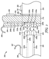
図1は、本開示の一態様による光コネクタ100の斜視概略図を示す。1つの特定の実施形態において、PCB基板120は、第1の表面122と、任意のマイクロレンズポケット140内に配設された複数の千鳥状に配置されたビア128a、128b、128c、128dを有する、対向する第2の表面124と、を有する。複数の千鳥状に配置されたビア128a、128b、128c、128dのそれぞれは、PCB基板120を貫通して、それぞれ関連する埋め込み式光導波路132a、132b、132c、132d、及び関連する光抽出部136a、136b、136c、136dが露出している深さまで延在している。
FIG. 1 illustrates a perspective schematic view of an
複数の千鳥状に配置されたビア128a、128b、128c、128dのそれぞれは、本明細書の他の箇所に記載されているように、マイクロレンズ径Dを有するマイクロレンズ(図示せず)を受容するように構成され、埋め込み式光導波路132a、132b、132c、132dの離隔距離に対応する中心間間隔L1で、任意のマイクロレンズポケット140内に配設されている。しかしながら、千鳥状のマイクロレンズ128a、128b、128c、128dのそれぞれは、マイクロレンズの離隔距離に対応する千鳥状の間隔L2を有し、千鳥状の間隔L2は、中心間間隔L1よりも大きい。結果的に、千鳥状の間隔L2のコネクタ内で使用可能な最大マイクロレンズ径Dは、他の箇所に記載するように、千鳥状ではないビアのマイクロレンズ間隔L1で使用可能な最大マイクロレンズ径よりも大きい。
Each of the plurality of staggered vias 128a, 128b, 128c, 128d receives a microlens (not shown) having a microlens diameter D, as described elsewhere herein. And is arranged in an
より大きい千鳥状のマイクロレンズ径D2が好ましい。任意のマイクロレンズポケット140の深さは、第1の表面122の位置よりも下にマイクロレンズそれぞれを保持するように機能する。PCB基板120は、任意の所望する数の、光抽出器136a〜136dと、千鳥状に配置されたビア128a〜128dと、千鳥状に配置されたビア128a〜128dの列と、各列に配置された千鳥状のビア128a〜128dと、埋め込まれた光導波路132a〜132dと、を含み得ることを理解すべきである。
A larger staggered microlens diameter D2 is preferred. The depth of the
この特定の実施形態において、2列のマイクロレンズ、及びその各列にある2個の千鳥状に配置されたビアが示されている。250マイクロメートルのファイバー間隔を有する光導波路で使用される場合、これによって関連するマイクロレンズ径を500マイクロメートルに近づけることができる。千鳥状に配置されたファイバー/マイクロレンズの実施形態で可能な500マイクロメートル径のコリメートマイクロレンズを使用すると、千鳥状に配置されていないビアで可能な250マイクロメートル径マイクロレンズに要求されるほど厳しくない位置合わせ許容誤差が可能になる。本明細書に記載のいかなる光コネクタも、千鳥状の光方向転換機構と、図1を参照して説明した、対応する千鳥状のマイクロレンズと、を含んでよく、可能な限り千鳥状構成を含むことが好ましい場合があることを理解すべきである。概して、上記の千鳥状のマイクロレンズ設計は、リボン化されたファイバー群に使用可能な拡大ビーム光導波路コネクタを実現可能にし、マイクロレンズから出射する光ビーム径は、リボン内でのファイバー間の離隔距離(つまり、ピッチ)よりも大きく、接続を達成するために、ファイバーを分離する必要はない。 In this particular embodiment, two rows of microlenses and two staggered vias in each row are shown. When used with optical waveguides having a fiber spacing of 250 micrometers, this allows the associated microlens diameter to approach 500 micrometers. The use of a 500 micrometer diameter collimated microlens that is possible in a staggered fiber / microlens embodiment is required for a 250 micrometer diameter microlens that is possible with vias that are not staggered. Less stringent alignment tolerances are possible. Any optical connector described herein may include a staggered light redirecting mechanism and a corresponding staggered microlens described with reference to FIG. It should be understood that it may be preferable to include. In general, the staggered microlens design described above allows for an expanded beam optical waveguide connector that can be used for ribboned fibers, where the diameter of the light beam emerging from the microlens is the separation between the fibers within the ribbon. There is no need to separate the fibers to achieve a connection that is greater than the distance (ie, pitch).
図2は、本開示の一態様による、PCB光配線200の断面側面図を示す。光配線200は、第2のPCB 220内に形成されたスロット205を介して第2のPCB 220と垂直の向きに接続された第1のPCB 210を含む。第1及び第2のPCB 210、220のそれぞれは、図1に示されているものと同様に千鳥状の向きに配置された複数の光導波路を含む。第1及び第2のPCB 210、220のそれぞれにおける複数の光導波路のうちの2つのみが図2に示されているが、光配線200には任意の数の千鳥状光導波路があってよいことを理解すべきである。第1のPCB 210は、第1のPCB 210内に配設された、第1の光抽出部236aを有する第1の光導波路232aと、第2の光抽出部236bを有する第2の光導波路232bと、を含む。第1のPCB 210は、また、複数の任意の電気光学装置264と、本明細書の他の箇所で記載されているように、他の構成要素に接続できる光ケーブル265と、を含むことできる。
FIG. 2 illustrates a cross-sectional side view of a PCB
第2のPCB 220は、第2のPCB 220内に配設された、第1の端部246aを有する第3の光導波路242aと、第2の端部246bを有する第4の光導波路242bと、を含む。第2のPCB 220は、また、複数の任意の電気光学装置266と、本明細書の他の箇所で記載されているように、他の構成要素に接続できる光ケーブル267と、を含むことができる。スロット205は、第1のPCB 210、及び2つのPCBを取付けるための電気コネクタ(図示せず)などの機構を収容するために、PCB 220に対して割り込み得る。
The
図2に表される図は、第1のPCB 210内の第1の光導波路232a、及び第2のPCB 220内の対応する第3の光導波路242aを通して生成された平面を通る断面を示すことを理解すべきである。千鳥状の第2の光導波路232b、及び千鳥状の第4の光導波路242b、並びに関連する構成要素が、それぞれ第1及び第2のPCB 210、220内の点線で参考として示されているが、これらが配置されている平面は、第1のPCB 210内の第1の光導波路232a、及び第2のPCB 220内の対応する第3の光導波路242aを通して生成された平面とは異なる。
The diagram depicted in FIG. 2 shows a cross-section through the plane generated through the first
第1のPCB 210及び第2のPCB 220は、例えば、第1の電気パッド261を有する任意の第1の電子デバイス260が、第2の電気パッド263を有する任意の第2の電子デバイス262と接続し、電気的接触269するように、電気コネクタ(図示せず)を介して電気的に接触し得る。第1及び第2のPCB 210、220間の対応する光接続が、本明細書の他の箇所に記載されているように、光導波路それぞれに関連するマイクロレンズを通して形成されている。
The
第1のマイクロレンズ234aが、第1の光導波路232aの第1の光抽出部236aからの第1の光250aを受容するために、第1の光ビア228a内に配設されている。図2に示されているように、第1の光抽出部236aは、第1の光導波路232aの傾斜劈開端部であり得るが、本明細書に記載されている任意の光抽出技術が代用し得ることを理解すべきである。第1の光250aは、第1のマイクロレンズ234aを通過し、第1のマイクロレンズ234aと、第3の光導波路242aの第1の端部246aに隣接して配設された第3のマイクロレンズ244aとの間の離間距離「S」を横切る時に広がる。第1の光250aは第3のマイクロレンズ244aを通過する時、第1の端部246aを通って第3の光導波路242aに進入するように集束される。
A
第4のマイクロレンズ244bは、第2の光250bが、第4のマイクロレンズ244bを通過し、第4のマイクロレンズ244bと第2のマイクロレンズ234bとの間の離間距離「S」を横切る時に広がるように、第4の光導波路242bの第2の端部246bに隣接して配設される。第2のマイクロレンズ234bは、第2の光ビア228b内に埋め込まれており、第2の光250bを第2の光抽出部236bに集束し、第2の光導波路232bに進入する。図2に示されているように、第2の光抽出部236bは、第2の光導波路232bの傾斜劈開端部であり得るが、本明細書に記載されている任意の光抽出技術が代用し得ることを理解すべきである。
The
第1及び第2の光導波路232a、232bは、第1のPCB 210に埋め込まれた光導波路であると図2で示されているが、場合によっては、代わりに第1のPCB 210の表面上に配設してもよいことを理解すべきである。この場合、対応する第1及び第2のマイクロレンズ234a、234bは、第1のPCB 210の表面の上方に配設し得る。また、場合によっては、第3及び第4の光導波路242a、242bは、第3及び第4のマイクロレンズ244a、244bも、ビア(図示せず)を介して配置され、PCB 220の中に部分的に埋め込まれるように、第2のPCB 220の更に中に配置し得ることも理解すべきである。
Although the first and second
更に、第1の光250aは、第1の光導波路232aから光配線200を通って第3の光導波路242aに進むと示されており、第2の光250bは、第4の光導波路242bから光配線200を通って第2の光導波路232aに進むと示されているが、対応する第1及び第2の光のそれぞれは、代わりに、反対方向に進み得ることを理解すべきである。換言すれば、光配線200は、双方向性の光配線であり得る。
Furthermore, the
図3は、本開示の一態様による、PCB光配線300の断面側面図を示す。図3に示されている要素310〜367のそれぞれは、上記の図2に示されている同様の参照符合で示された要素に対応している。例えば、図3の第1の光導波路332aは、図2の第1の光導波路232aに対応しているなど。図3で示されている図は、図2に表されそれを参照して説明されている図と同様に、それぞれの光導波路の断面を示していることを理解すべきである。
FIG. 3 illustrates a cross-sectional side view of a PCB
光配線300は、第2のPCB 320に垂直方向に接続され、第1のPCB 310内に形成され第2のPCB 320内に形成された第2のコネクタ要素377と嵌合された第1のコネクタ要素375を使用して固定された、第1のPCB 310を含む。第1及び第2のコネクタ要素375、377は、2つのPCBをともにしっかり締結する機構を含むことができ、また、本明細書の他の箇所で記載されているように、追加の電気的接触も含み得る。第1及び第2のPCB 310、320のそれぞれは、図1に示されているものと同様に千鳥状の向きに配置された複数の光導波路を含む。第1及び第2のPCB 310、320のそれぞれにおける複数の光導波路のうちの2つのみが図3に示されているが、光配線300には任意の数の千鳥状光導波路があってよいことを理解すべきである。第1のPCB 310は、第1のPCB 310内に配設された、第1の光抽出部336aを有する第1の光導波路332aと、第2の光抽出部336bを有する第2の光導波路332bと、を含む。第1のPCB 310は、また、複数の任意の電気光学装置364と、本明細書の他の箇所で記載されているように、他の構成要素に接続できる光ケーブル365と、を含み得る。
The
第2のPCB 320は、第2のPCB 320内に配設された、第3の光抽出部346aを有する第3の光導波路342aと、第4の光抽出部346bを有する第4の光導波路342bと、を含む。第2のPCB 320は、また、複数の任意の電気光学装置366と、本明細書の他の箇所で記載されているように、他の構成要素に接続できる光ケーブル367と、を含み得る。第1のPCB 310及び第2のPCB 320は、例えば、第1の電気パッド361を有する任意の第1の電子デバイス360が、第2の電気パッド363を有する任意の第2の電子デバイス362と接続し、電気的接触369するように、第1及び第2のコネクタ要素375、377を介して電気的に接触し得る。第1及び第2のPCB 310、320間の対応する光接続が、本明細書の他の箇所に記載されているように、光導波路それぞれに関連するマイクロレンズを通して形成されている。
The
反射面376と、第1のマイクロレンズ371と、第2のマイクロレンズ372と、第1の表面373と、を含む光方向転換要素370が、PCBのうちの1つから出る光が他のPCBに進入するように方向転換されるように、第1のコネクタ要素375の中に配設されている。場合によっては、光方向転換要素370は、1つの表面上にマイクロレンズを有するプリズムであってよい。場合によっては(図示せず)、光方向転換要素370は、代わりに、ミラー及びマイクロレンズの分離したアレイなどの反射器を有し得る。光方向転換要素370は、当業者には公知の通り、第1のPCB 310又は第2のPCB 320のいずれかに付ける(又は、第1又は第2のコネクタ要素375、377のいずれかの構造体又は機構に関連付ける)ことができると理解すべきである。
A
光ビア378は、第1の光導波路332aの第1の光抽出部336a、及び第2の光導波路232bの第2の光抽出部336bを露光する。光方向転換要素370の第1のマイクロレンズ371は、第1の光導波路232aの第1の光抽出部336aからの第1の光350aを受容するように配設されている。第1の光350aは、第1のマイクロレンズ371を通過し、反射面376を反射し、第1の表面373を通って光方向転換要素370を出て、第3のマイクロレンズ244aに進入する。第3のマイクロレンズ244aは、第2のPCB 320内の第3の光ビア348aの中に配設されており、第2のPCB 320は、第3の光導波路342aの第3の光抽出部346aを露光する。第1の光350aは、第3の光抽出部346a上に集束され、第3の光導波路342aの中に注入される。
The optical via 378 exposes the first light extraction unit 336a of the first
第4のマイクロレンズ344bは、第2のPCB 320内の第4の光ビア348bの中に配設され、第2のPCB 320は、第4の光導波路342aから抽出された第2の光350bが、第4のマイクロレンズ344bを通過し、第1の表面373を通って光方向転換要素370に進入するように、第4の光導波路342bの第4の光抽出部346bを露光する。第2の光350bは、反射面376で反射し、第2のマイクロレンズ372を通過し、第2の光抽出部336bで集束され、第2の光導波路332bに進入する。
The
図2での説明と同様に、図3に示されている光抽出部は光導波路の傾斜劈開端部であり得るが、本明細書に記載されている任意の光抽出技術が代用し得ることを理解すべきである。更に、光導波路のそれぞれは、図2を参照して説明されている場合と同様に、各PCBに埋め込まれていてもよいし、又は各PCBの表面上に配設されていてもよいことを理解すべきである。更に、光配線300は、本明細書の他の箇所で記載されているように、双方向性の光配線であり得る。
Similar to the description in FIG. 2, the light extraction section shown in FIG. 3 can be an inclined cleaved end of an optical waveguide, but any light extraction technique described herein can be substituted. Should be understood. Further, each of the optical waveguides may be embedded in each PCB, or may be disposed on the surface of each PCB, as in the case described with reference to FIG. Should be understood. Furthermore, the
図4Aは、本開示の一態様による、PCB光配線400の断面側面図を示す。図4に示されている要素410〜477のそれぞれは、上記の図3に示されている同様の参照符合で示された要素に対応している。例えば、図4Aの第1の光導波路432aは、図3の第1の光導波路332aに対応しているなど。図4に示されている図は、図2及び図3に表されそれを参照して説明されている図と同様に、それぞれの光導波路の断面を示していることを理解すべきである。
FIG. 4A shows a cross-sectional side view of a PCB
光配線400は、第2のPCB 420に垂直方向に接続され、第2のPCB 420内に形成され第1のPCB 410内に形成された第2のコネクタ要素477と嵌合された第1のコネクタ要素475を使用して固定された、第1のPCB 410を含む。第1及び第2のコネクタ要素475、477は、2つのPCBをともにしっかり締結する機構を含むことができ、また、本明細書の他の箇所で記載されているように、追加の電気的接触も含み得る。第1及び第2のPCB 410、420のそれぞれは、図1に示されているものと同様に千鳥状の向きに配置された複数の光導波路を含む。第1及び第2のPCB 410、420のそれぞれにおける複数の光導波路のうちの2つのみが図4Aに示されているが、光配線400には任意の数の千鳥状光導波路があってよいことを理解すべきである。第1のPCB 410は、第1のPCB 410内に配設された、第1の光抽出部436aを有する第1の光導波路432aと、第2の光抽出部436bを有する第2の光導波路432bと、を含む。第1のPCB 410は、また、複数の任意の電気光学装置464と、本明細書の他の箇所で記載されているように、他の構成要素に接続できる光ケーブル465と、を含み得る。
The
第2のPCB 420は、第2のPCB 420内に配設された、第3の光抽出部446aを有する第3の光導波路442aと、第4の光抽出部446bを有する第4の光導波路442bと、を含む。第2のPCB 420は、また、複数の任意の電気光学装置466と、本明細書の他の箇所で記載されているように、他の構成要素に接続できる光ケーブル467と、を含み得る。第1のPCB 410及び第2のPCB 420は、例えば、第1の電気パッド461を有する任意の第1の電子デバイス460が、第2の電気パッド463を有する任意の第2の電子デバイス462と接続し、電気的接触469するように、第1及び第2のコネクタ要素475、477を介して電気的に接触し得る。第1及び第2のPCB 410、420間の対応する光接続が、本明細書の他の箇所に記載されているように、光導波路それぞれに関連するマイクロレンズを通して形成されている。
The
反射面476と、第4のマイクロレンズ471と、第3のマイクロレンズ472と、第1の表面473とを含む光方向転換要素470が、PCBのうちの1つから出る光が他のPCBに進入するように方向転換されるように、第1のコネクタ要素475の中に配設されている。場合によっては、光方向転換要素470は、1つの表面上にマイクロレンズを有するプリズムであってよい。場合によっては(図示せず)、光方向転換要素470は、代わりに、ミラー及びマイクロレンズの分離したアレイなどの反射器を含み得る。光方向転換要素470は、当業者には公知の通り、第1のPCB 410又は第2のPCB 420のいずれかに付ける(又は、第1又は第2のコネクタ要素475、477のいずれかの構造体又は機構に関連付ける)ことができると理解すべきである。
A
第1の光ビア428aは、第1の光導波路432aの第1の光抽出部436aを露光し、第2の光ビア428bは、第2の導波路232bの第2の光抽出部436bを露光する。第1のマイクロレンズ424aは、第1の光導波路432aの第1の光抽出部436aからの第1の光450aを受容するように配設されている。第1の光450aは、第1のマイクロレンズ424aを通過し、第1の表面473に進入し、反射面476を反射し、第3のマイクロレンズ472を通って光方向転換要素470を出る。第3のマイクロレンズ472は、第2のPCB 420内の光ビア474によって露光された第3の光導波路442aの第3の光抽出部446aに第1の光450aを集束し、それによって第1の光450aを第3の光導波路442aに注入するように配設される。
The first optical via 428a exposes the first
第2のPCB 420内の光ビア474は、第4の光導波路442b内を進む光が、第4のマイクロレンズ471を通過するように配向され、反射面476を反射し、第1の表面473を通って光方向転換要素470を出て、第2のマイクロレンズ424bによって第2の光抽出部436b上に集束され、第2の光導波路432b内に注入されるように、第4の光導波路442bの第4の光抽出部446bを露光する。場合によっては、光ビア474は、代わりに、第3及び第4の光抽出部446a、446bを別々に露光する別個の光ビア(図示せず)で形成され得る。
The optical via 474 in the
図2及び図3での説明と同様に、図4Aに示されている光抽出部は光導波路の傾斜劈開端面であり得るが、本明細書に記載されている任意の光抽出技術が代用し得ることを理解すべきである。更に、光導波路のそれぞれは、図2及び図3を参照して説明されている場合と同様に、各PCBに埋め込まれていてもよいし、又は各PCBの表面上に配設されていてもよいことを理解すべきである。更に、光配線400は、本明細書の他の箇所で記載されているように、双方向性の光配線であり得る。
Similar to the description in FIGS. 2 and 3, the light extraction section shown in FIG. 4A can be an inclined cleaved end face of the optical waveguide, but any light extraction technique described herein can be substituted. It should be understood that you get. Further, each of the optical waveguides may be embedded in each PCB, or may be disposed on the surface of each PCB, as in the case described with reference to FIGS. 2 and 3. It should be understood. Furthermore, the
図4Bは、本開示の一態様による、PCB光配線401の断面側面図を示す。図4Bに示される要素410〜477のそれぞれは、上記の図4Aに示される類似の参照符合の要素に対応している。例えば、図4Aの第の1の光導波路432aは、図4Bの第1の光導波路432aに対応しているなど。図4Bで示されている図は、図4Aに表されそれを参照して説明されている図と同様に、それぞれの光導波路の断面を示していることを理解すべきである。
FIG. 4B shows a cross-sectional side view of PCB
光配線401は、第2のPCB 420に垂直方向に接続され、第2のPCB 420内に形成され第1のPCB 410内に形成された第2のコネクタ要素477と嵌合された第1のコネクタ要素475を使用して固定された、第1のPCB 410を含む。第1及び第2のコネクタ要素475、477は、2つのPCBをともにしっかり締結する機構を含むことができ、また、本明細書の他の箇所で記載されているように、追加の電気的接触も含み得る。第1及び第2のPCB 410、420のそれぞれは、図1に示されているものと同様に千鳥状の向きに配置された複数の光導波路を含む。第1及び第2のPCB 410、420のそれぞれにおける複数の光導波路のうちの2つのみが図4Bに示されているが、光配線401には任意の数の千鳥状光導波路があってよいことを理解すべきである。第1のPCB 410は、第1のPCB 410内に配設された、第1の光抽出部436aを有する第1の光導波路432aと、第2の光抽出部436bを有する第2の光導波路432bと、を含む。第1のPCB 410は、また、複数の任意の電気光学装置464と、本明細書の他の箇所で記載されているように、他の構成要素に接続できる光ケーブル465と、を含み得る。
The
第2のPCB 420は、第2のPCB 420内に配設された、第3の光抽出部446aを有する第3の光導波路442aと、第4の光抽出部446bを有する第4の光導波路442bと、を含む。第2のPCB 420は、また、複数の任意の電気光学装置466と、本明細書の他の箇所で記載されているように、他の構成要素に接続できる光ケーブル467と、を含み得る。第1のPCB 410及び第2のPCB 420は、例えば、第1の電気パッド461を有する任意の第1の電子デバイス460が、第2の電気パッド463を有する任意の第2の電子デバイス462と接続し、電気的接触469するように、第1及び第2のコネクタ要素475、477を介して電気的に接触し得る。第1及び第2のPCB 410、420間の対応する光接続が、本明細書の他の箇所に記載されているように、光導波路それぞれに関連するマイクロレンズを通して形成されている。
The
反射面476と、第1の表面473と、第2の表面479と、を含む光方向転換要素470’は、PCBのうちの1つから出る光が他のPCBに進入するように方向転換されるように、第1のコネクタ要素475の中に配設されている。場合によっては、光方向転換要素470’はプリズムであってよい。場合によっては(図示せず)、光方向転換要素470’は、代わりに、ミラーなどの反射器を含み得る。光方向転換要素470’は、当業者には公知の通り、第1のPCB 410又は第2のPCB 420のいずれかに付ける(又は、第1又は第2のコネクタ要素475、477のいずれかの構造体又は機構に関連付ける)ことができると理解すべきである。
A
第1の光ビア428aは、第1の光導波路432aの第1の光抽出部436aを露光し、第2の光ビア428bは、第2の導波路232bの第2の光抽出部436bを露光する。第1のマイクロレンズ424aは、第1の光導波路432aの第1の光抽出部436aからの第1の光450aを受容するように配設されている。第1の光450aは、第1のマイクロレンズ424aを通過し、第1の表面473に進入し、反射面476を反射し、第2の表面479を通って光方向転換要素470’を出る。第3のマイクロレンズ444aは、第2のPCB 420内の第3の光ビア448によって露光された第3の光導波路442aの第3の光抽出部446aに第1の光450aを集束し、それによって第1の光450aを第3の光導波路442a内に注入する。
The first optical via 428a exposes the first
第2のPCB 420内の第4の光ビア448bは、第4の光導波路442b内を進む光が、第4のマイクロレンズ444bを通過するように向けられ、光方向転換要素470’の第2の表面479に進入し、反射面476を反射し、第1の表面473を通って光方向転換要素470’を出て、第2のマイクロレンズ424bによって第2の光抽出部436bに集束され、第2の光導波路432bに注入されるように、第4の光導波路442bの第4の光抽出部446bを露光する。
The fourth optical via 448b in the
図4Aでの説明と同様に、図4Bに示されている光抽出部は光導波路の傾斜劈開端面であり得るが、本明細書に記載されている任意の光抽出技術が代用し得ることを理解すべきである。更に、光導波路のそれぞれは、図4Aを参照して説明されている場合と同様に、各PCBに埋め込まれていてもよいし、又は各PCBの表面上に配設されていてもよいことを理解すべきである。更に、光配線401は、本明細書の他の箇所で記載されているように、双方向性の光配線であり得る。
Similar to the description in FIG. 4A, the light extraction section shown in FIG. 4B can be an inclined cleaved end face of an optical waveguide, but any light extraction technique described herein can be substituted. Should be understood. Further, each of the optical waveguides may be embedded in each PCB, or may be disposed on the surface of each PCB, as described with reference to FIG. 4A. Should be understood. Furthermore, the
図4Cは、本開示の一態様による、PCB光配線402の断面側面図を示す。図4Cに示されている要素410〜477のそれぞれは、上記の図4Aに示されている類似の参照符合の要素に対応している。例えば、図4Cの第1の光導波路432aは、図4Bの第1の光導波路432aに対応しているなど。図4Cで示されている図は、図4Aに表されそれを参照して説明されている図と同様に、それぞれの光導波路の断面を示していることを理解すべきである。
FIG. 4C illustrates a cross-sectional side view of the PCB
光配線402は、第2のPCB 420に垂直方向に接続され、第2のPCB 420内に形成され第1のPCB 410内に形成された第2のコネクタ要素477と嵌合された第1のコネクタ要素475を使用して固定された、第1のPCB 410を含む。第1及び第2のコネクタ要素475、477は、2つのPCBをともにしっかり締結する機構を含むことができ、また、本明細書の他の箇所で記載されているように、追加の電気的接触も含み得る。第1及び第2のPCB 410、420のそれぞれは、図1に示されているものと同様に千鳥状の向きに配置された複数の光導波路を含む。第1及び第2のPCB 410、420における複数の光導波路のうちの2つのみが図4Cに示されているが、光配線402には任意の数の千鳥状光導波路があってよいことを理解すべきである。第1のPCB 410は、第1のPCB 410内に配設された、第1の光抽出部436aを有する第1の光導波路432aと、第2の光抽出部436bを有する第2の光導波路432bと、を含む。第1のPCB 410は、また、複数の任意の電気光学装置464と、本明細書の他の箇所で記載されているように、他の構成要素に接続できる光ケーブル465と、を含み得る。
The
第2のPCB 420は、第2のPCB 420内に配設された、第3の光抽出部446aを有する第3の光導波路442aと、第4の光抽出部446bを有する第4の光導波路442bと、を含む。第2のPCB 420は、また、複数の任意の電気光学装置466と、本明細書の他の箇所で記載されているように、他の構成要素に接続できる光ケーブル467と、を含み得る。第1のPCB 410及び第2のPCB 420は、例えば、第1の電気パッド461を有する任意の第1の電子デバイス460が、第2の電気パッド463を有する任意の第2の電子デバイス462と接続し、電気的接触469するように、第1及び第2のコネクタ要素475、477を介して電気的に接触し得る。第1及び第2のPCB 410、420間の対応する光接続が、本明細書の他の箇所に記載されているように、光導波路それぞれに関連するマイクロレンズを通して形成されている。
The
反射面476と、第2のマイクロレンズ472’に隣接した第1のマイクロレンズ471’と、第4のマイクロレンズ471に隣接した第3のマイクロレンズ472と、を含む光方向転換要素470’’は、PCBのうちの1つから出る光が他のPCBに進入するように方向転換されるように、第1のコネクタ要素475の中に配設されている。場合によっては、光方向転換要素470’’はプリズムであり得、各隣接するマイクロレンズのセットはプリズムの直交面上に配設し得る。場合によっては(図示せず)、光方向転換要素470’’は、代わりに、ミラー及びマイクロレンズの2つの直交アレイなどの反射器を含み得る。光方向転換要素470’’は、当業者には公知の通り、第1のPCB 410又は第2のPCB 420のいずれかに付ける(又は、第1又は第2のコネクタ要素475、477のいずれかの構造体又は機構に関連付ける)ことができると理解すべきである。
A light redirecting element 470 '' including a
第1の光ビア478は、第1の光導波路432aの第1の光抽出部436a、及び第2の光導波路232bの第2の光抽出部436bを露光でき、又は別個の光ビアを両方に使用してもよい(図示せず)。第1のマイクロレンズ471’は、第1の光導波路432aの第1の光抽出部436aからの第1の光450aを受容するように配設されている。第1の光450aは、第1のマイクロレンズ471’を通過し、反射面476を反射し、第3のマイクロレンズ472を通って光方向転換要素470’を出る。第3のマイクロレンズ472は、第2の光ビア474によって露光された第3の光導波路442aの第3の光抽出部446aに第1の光450aを集束し、それによって第1の光450aを第3の光導波路442a内に注入する。
The first optical via 478 can expose the first
第2のPCB 420内の第2の光ビア474は、また、第4の光導波路442b内を進む光が、第4のマイクロレンズ471を通過するように向けられ、反射面476を反射し、光方向転換要素470’’を出て、第2のマイクロレンズ472’によって第2の光抽出部436b上に集束され、第2の光導波路432bに注入されるように、第4の光導波路442bの第4の光抽出部446bを露光する。
The second optical via 474 in the
図4Aでの説明と同様に、図4Cに示されている光抽出部は光導波路の傾斜劈開端面であり得るが、本明細書に記載されている任意の光抽出技術が代用し得ることを理解すべきである。更に、光導波路のそれぞれは、図4Aを参照して説明されている場合と同様に、各PCBに埋め込まれていてもよいし、又は各PCBの表面上に配設されていてもよいことを理解すべきである。更に、光配線402は、本明細書の他の箇所で記載されているように、双方向性の光配線であり得る。
Similar to the description in FIG. 4A, the light extraction section shown in FIG. 4C can be an inclined cleaved end face of an optical waveguide, but any light extraction technique described herein can be substituted. Should be understood. Further, each of the optical waveguides may be embedded in each PCB, or may be disposed on the surface of each PCB, as described with reference to FIG. 4A. Should be understood. Furthermore, the
図5は、本開示の一態様による、接続されたPCB 500の端面図を示す。接続されたPCB 500は、第1のブレードPCB 520a及び第2のブレードPCB 520bがバックプレーンPCB 510の第1の主表面512に接続されたバックプレーンPCB 510を含む。図5の光導波路は、通常、各PCBの中に埋め込まれるか、又は対応するPCBの表面上若しくは上部に配設し得る光導波路又は電気光学的導波路であり得ることを理解すべきである。更に、当業者には公知の通り、様々な構成要素間を電気的に接続し得る。更に、電気光学装置、配線及びブレードPCBの相対的配置及び数は、例示のみを目的としたものであって、当業者には公知の通り、任意の所望の数及び配置が使用し得ることを理解すべきである。
FIG. 5 illustrates an end view of a
1つの特定の実施形態において、第1のブレードPCB 520aは、第1のブレードPCB 520aの同じ表面上又は異なる表面上に配設された、任意の第1の電気光学装置562と、任意の第2の電気光学装置564と、を含む。第1のブレードPCB 520aは、第1の光コネクタ568、及び第1の電気光学的コネクタ560を介してバックプレーンPCB 510に接続され得る。第1の光コネクタ568は、図2〜4Cを参照して説明されている光配線200、300、及び400〜402のうちのいずれかを含み得る。場合によっては、第1の電気光学的コネクタ560は、第1の光導波路561を使用して任意の第1の電気光学装置562に接続し得る。
In one particular embodiment, the
1つの特定の実施形態において、第2のブレードPCB 520bは、第2のブレードPCB 520bの同じ表面上又は異なる表面上に配設された、任意の第3の電気光学装置566と、任意の第4の電気光学装置572と、任意の第5の電気光学装置574と、を含む。第2のブレードPCB 520bは、第2の光コネクタ570、及び第2の電気光学的コネクタ576を介してバックプレーンPCB 510に接続され得る。第2の光コネクタ570は、図2〜4Cを参照して説明されている光配線200、300、及び400〜402のうちのいずれかを含み得る。場合によっては、(第2のブレードPCB 520b上の)任意の第3の電気光学装置566は、(第1のブレードPCB 520a上の)任意の第2の電気光学装置564に接続でき、第2の電気光学的コネクタ576は、第3の光導波路575を使用して任意の第5の電気光学装置574に接続でき、任意の第5の電気光学装置574は、第4の光導波路573を使用して任意の第4の電気光学装置572に接続できる。場合によっては、バックプレーンPCB 510の第1の主表面512上の第6の電気光学装置578に接続された第5の光導波路579を介するなど、他の外部システム(図示せず)に接続することもできる。
In one particular embodiment, the
任意に、バックプレーンPCB 510の第1の主表面512から第2の主表面514までを電気的、光学的、又は電気光学的に接続することができる。1つの特定の実施形態において、第1の光コネクタ568は、第1の裏面側コネクタ584を介してバックプレーンPCB 510の第2の主表面514と電気的、光学的、又は電気光学的に接続していることができ、第2の光コネクタ570は、第2の裏面側コネクタ582を介してバックプレーンPCB 510の第2の主表面514と電気的、光学的、又は電気光学的に接続していることができる。第1の裏面側コネクタ584は更に、それぞれ第1、第2、第3の裏面側光導波路583、585、587を使用して、第1の裏面側電気光学装置586、及び第2の裏面側コネクタ582などの他の任意の装置に接続し得る。第2の裏面側コネクタ582は更に、第4の裏面側光導波路581によって第2の裏面側電気光学装置580に接続し得る。
Optionally, the first
図6A〜6Cは、本開示の一態様による、光抽出部の実施形態の概略図を示す。図6Aは、プリズム634の入力面631に隣接して配置された端部633aを有する光導波路632aを示す。プリズム634は、反射斜面636と、出力面635と、を含む。光導波路632a内を進む光650aは、プリズム634の入力面631に進入し、反射斜面636を反射し、出力面635を通ってプリズム634から異なる方向に出る。反射斜面636は、光650aがTIRで反射するように磨かれた面であってよく、あるいは誘電体スタック又は有機材料若しくは無機材料を含む反射層を含んでもよく、又は反射性金属を含んでもよい。場合によっては、プリズム634は、代わりに、端部633aに対して同じ位置に反射斜面636として配置される平面鏡(図示せず)に交換されてもよい。場合によっては、プリズム634は、代わりに、本明細の他の箇所に記載されているように、光導波路632aを劈開して反射斜面636を作り出すことで交換されてもよい。
6A-6C illustrate schematic diagrams of embodiments of light extraction units, according to one aspect of the present disclosure. FIG. 6A shows an
図6Bは、端部633bと、光導波路632bの表面上に配設された光抽出グレーティング637と、を有して、当業者には公知の通り、抽出された光が光導波路から異なる方向に出るように、光導波路632b内を進む光650bを抽出する、光導波路632bを示す。場合によっては、光抽出グレーティング637は、1つの特定の波長の光650bを光導波路632bから抽出するように設計し得る。 FIG. 6B includes an end 633b and a light extraction grating 637 disposed on the surface of the optical waveguide 632b so that the extracted light is in a different direction from the optical waveguide as known to those skilled in the art. Shown is an optical waveguide 632b that extracts light 650b traveling through the optical waveguide 632b as it exits. In some cases, the light extraction grating 637 may be designed to extract one particular wavelength of light 650b from the optical waveguide 632b.
図6Cは、端部633cと、第1の光抽出グレーティング638と、光導波路632cの表面上に配設された第2の光抽出グレーティング639と、を有する光導波路632cを示す。第1の光抽出グレーティング638は、第1の波長を有する第1の光650cを抽出するように配設され、第2の光抽出グレーティング639は、第2の波長を有する第2の光651cを抽出するように配設され、いずれの光も、抽出された光が光導波路から異なる方向に出るように光導波路632b内を進む。
FIG. 6C shows an
以下は、本開示の実施形態の一覧である。 The following is a list of embodiments of the present disclosure.
項目1は、第1のPCBと、第1のPCBの上又は中に配設された光抽出部を有する複数の第1の光導波路であって、光抽出部が互いに千鳥状に配置されている、複数の第1の光導波路と、を備える第1のプリント基板(PCB)アセンブリと、電気コネクタを介して第1のPCBの第1の側に接続された第2のPCBと、第2のPCBの上又は中に配設された光抽出部を有する複数の第2の光導波路であって、光抽出部が互いに千鳥状に配置され、複数の第2の光導波路における各第2の光導波路が、複数の第1の光導波路における異なる第1の光導波路に対応している、複数の第2の光導波路と、互いに千鳥状に配置された複数の第1のマイクロレンズであって、複数の第1のマイクロレンズにおける各第1のマイクロレンズが、複数の第1の光導波路における異なる第1の光導波路に対応している、複数の第1のマイクロレンズと、互いに千鳥状に配置された複数の第2のマイクロレンズであって、複数の第2のマイクロレンズにおける各第2のマイクロレンズが、複数の第2の光導波路における異なる第2の光導波路に対応している、複数の第2のマイクロレンズと、を備える光配線アセンブリであって、複数の第1の光導波路における各第1の光導波路の光抽出部と、複数の第2の光導波路における対応する第2の光導波路は、第1の光導波路内を進む光が、第1の光導波路の光抽出部によって方向転換された後で第2の光導波路に進入し、第1光導波路を出て、第1の光導波路に対応する複数の第1のマイクロレンズにおける第1のマイクロレンズを通って進み、第2の光導波路に対応する複数の第2のマイクロレンズにおける第2のマイクロレンズを通って進み、第2の光導波路の光抽出部によって方向転換されるように配向される、光配線アセンブリである。 Item 1 is a plurality of first optical waveguides having a first PCB and a light extraction unit disposed on or in the first PCB, wherein the light extraction units are arranged in a staggered manner. A first printed circuit board (PCB) assembly comprising a plurality of first optical waveguides, a second PCB connected to a first side of the first PCB via an electrical connector, and a second A plurality of second optical waveguides having light extraction portions disposed on or in the PCB, wherein the light extraction portions are arranged in a staggered manner, and each second in the plurality of second optical waveguides The optical waveguide is a plurality of second optical waveguides corresponding to different first optical waveguides in the plurality of first optical waveguides, and a plurality of first microlenses arranged in a staggered manner. , Each first microlens in the plurality of first microlenses is a plurality of A plurality of first microlenses corresponding to different first optical waveguides in one optical waveguide, and a plurality of second microlenses arranged in a staggered manner, each having a plurality of second microlenses. A plurality of second microlenses, each second microlens in the lens corresponding to a different second optical waveguide in the plurality of second optical waveguides, The light extraction unit of each first optical waveguide in the first optical waveguide and the corresponding second optical waveguide in the plurality of second optical waveguides are such that light traveling in the first optical waveguide is transmitted through the first optical waveguide. The first microlens in the plurality of first microlenses corresponding to the first optical waveguide enters the second optical waveguide after being redirected by the light extraction unit of the waveguide, exits the first optical waveguide, and Proceed through the second Travels through the second micro-lens in the plurality of second micro lenses corresponding to the optical waveguide is oriented to be diverted by the light extraction portion of the second optical waveguide, an optical wiring assembly.
項目2は、光抽出部のそれぞれが、傾斜劈開端面、光方向転換プリズム、平面鏡、抽出グレーティング、又はこれらの組み合わせを具備する、項目1の光配線アセンブリである。 Item 2 is the optical wiring assembly of item 1, wherein each of the light extraction units includes an inclined cleavage end face, a light redirecting prism, a plane mirror, an extraction grating, or a combination thereof.
項目3は、第1及び第2のPCBのうちの1つが、バックプレーンPCBである、項目1又は項目2の光配線アセンブリである。 Item 3 is the optical wiring assembly of item 1 or item 2, wherein one of the first and second PCBs is a backplane PCB.
項目4は、第1のPCBが、その上に装着された少なくとも1つの第1の半導体チップを具備する、項目1〜項目3の光配線アセンブリである。 Item 4 is the optical wiring assembly of items 1 to 3, wherein the first PCB comprises at least one first semiconductor chip mounted thereon.
項目5は、第2のPCBが、その上に装着された少なくとも1つの第2の半導体チップを具備する、項目1〜項目4の光配線アセンブリである。 Item 5 is the optical wiring assembly of items 1 to 4, wherein the second PCB comprises at least one second semiconductor chip mounted thereon.
項目6は、第1及び第2のPCBのそれぞれが、その上に装着された少なくとも1つの半導体チップを具備する、項目1〜項目5の光配線アセンブリである。 Item 6 is the optical wiring assembly of items 1 to 5, wherein each of the first and second PCBs includes at least one semiconductor chip mounted thereon.
項目7は、第1及び第2のPCBのそれぞれの上に配設された少なくとも1つの電気光学装置を更に具備する、項目〜項目6の光配線アセンブリである。 Item 7 is the optical wiring assembly of items 6 to 6, further comprising at least one electro-optical device disposed on each of the first and second PCBs.
項目8は、少なくとも1つの電気光学装置が発光装置を具備する、項目7の光配線アセンブリである。 Item 8 is the optical wiring assembly of item 7, wherein at least one electro-optical device comprises a light emitting device.
項目9は、少なくとも1つの電気光学装置が光検出装置を具備する、項目7の光配線アセンブリである。 Item 9 is the optical wiring assembly of item 7, wherein at least one electro-optical device comprises a light detection device.
項目10は、複数の第1及び第2の光導波路における光導波路のうちの少なくともいくつかがそれぞれのPCB内に埋め込まれている、項目1〜項目9の光配線アセンブリである。 Item 10 is the optical wiring assembly of items 1 to 9, wherein at least some of the optical waveguides in the plurality of first and second optical waveguides are embedded in the respective PCBs.
項目11は、複数の第1の光導波路における複数の第1の光導波路を具備する第1の光ケーブルを更に具備し、第1の光ケーブルの第1の部分が第1のPCB上に配置され、第1の光ケーブルの第2の部分が第1のPCB上に配置されておらず、第1の部分が、複数の第1の光導波路における第1の光導波路の光抽出部を具備する、項目1〜項目10の光配線アセンブリである。 Item 11 further comprises a first optical cable comprising a plurality of first optical waveguides in the plurality of first optical waveguides, wherein the first portion of the first optical cable is disposed on the first PCB, The second portion of the first optical cable is not disposed on the first PCB, and the first portion includes the light extraction portion of the first optical waveguide in the plurality of first optical waveguides. 1 is an optical wiring assembly according to item 10.
項目12は、複数の第1の光導波路における各第1の光導波路が光ファイバーである、項目11の光配線アセンブリである。 Item 12 is the optical wiring assembly of item 11, wherein each first optical waveguide in the plurality of first optical waveguides is an optical fiber.
項目13は、複数の第2の光導波路における複数の第2の光導波路を具備する第2の光ケーブルを更に具備し、第2の光ケーブルの第1の部分が第2のPCB上に配置され、第2の光ケーブルの第2の部分が第2のPCB上に配置されておらず、第1の部分が、複数の第2の光導波路における第2の光導波路の光抽出部を具備する、項目1〜項目12の光配線アセンブリである。 Item 13 further comprises a second optical cable comprising a plurality of second optical waveguides in the plurality of second optical waveguides, wherein the first portion of the second optical cable is disposed on the second PCB, Item wherein the second portion of the second optical cable is not disposed on the second PCB, and the first portion includes the light extraction portion of the second optical waveguide in the plurality of second optical waveguides 1 is an optical wiring assembly according to item 12.
項目14は、複数の第2の光導波路における各第2の光導波路が光ファイバーである、項目13の光配線アセンブリである。 Item 14 is the optical wiring assembly of item 13, wherein each second optical waveguide in the plurality of second optical waveguides is an optical fiber.
項目15は、複数の第1のマイクロレンズと、複数の第2のマイクロレンズとの間に配設された光方向転換要素を更に具備し、複数の第1の光導波路における各第1の光導波路の光抽出部と、複数の第2の導波路における対応する第2の光導波路が、第1の光導波路内を進む光が、第1の光導波路の光抽出部によって方向転換された後で第2の光導波路に進入し、第1の光導波路を出て、第1の光導波路に対応する複数の第1のマイクロレンズにおける第1のマイクロレンズを通って進み、光方向転換要素によって方向転換され、第2の光導波路に対応する複数の第2のマイクロレンズを通って進み、第2の光導波路の光抽出部によって方向転換されるように配向されている、項目1〜項目14の光配線アセンブリである。 Item 15 further includes a light redirecting element disposed between the plurality of first microlenses and the plurality of second microlenses, and each first light guide in the plurality of first optical waveguides. After the light extraction unit of the waveguide and the corresponding second optical waveguides in the plurality of second waveguides travel in the first optical waveguide, the light is redirected by the light extraction unit of the first optical waveguide To enter the second optical waveguide, exit the first optical waveguide, proceed through the first microlenses in the plurality of first microlenses corresponding to the first optical waveguide, and by the light redirecting element Items 1 to 14 that are redirected and advanced through a plurality of second microlenses corresponding to the second optical waveguide and are redirected by the light extraction portion of the second optical waveguide. This is an optical wiring assembly.
項目16は、光方向転換要素が、内部全反射によって光を方向転換する、項目15の光配線アセンブリである。 Item 16 is the optical wiring assembly of item 15, wherein the light redirecting element redirects the light by total internal reflection.
項目17は、複数の第1のマイクロレンズにおける第1のマイクロレンズが、光方向転換要素の第1の主表面上に配設され、複数の第2のマイクロレンズにおける第2のマイクロレンズが、光方向転換要素の第2の主表面上に配設され、第2の主表面が、第1の主表面と斜角を成す、項目15又は項目16の光配線アセンブリである。 Item 17 is that the first microlenses in the plurality of first microlenses are disposed on the first main surface of the light redirecting element, and the second microlenses in the plurality of second microlenses are Item 15 or item 16 of the optical wiring assembly disposed on the second major surface of the light redirecting element, wherein the second major surface forms an oblique angle with the first major surface.
項目18は、光方向転換要素が、プリズム式である項目1〜項目17の光配線アセンブリである。 Item 18 is the optical wiring assembly of items 1 to 17, wherein the light redirecting element is a prism type.
項目19は、複数の第1のマイクロレンズにおける第1のマイクロレンズが、第1のPCB上に配設されている、項目1〜項目18の光配線アセンブリである。 Item 19 is the optical wiring assembly according to items 1 to 18, wherein the first microlenses of the plurality of first microlenses are arranged on the first PCB.
項目20は、複数の第1の光導波路における第1の光導波路が、第1のPCB内に埋め込まれている、項目19の光配線アセンブリである。 Item 20 is the optical wiring assembly of item 19, wherein the first optical waveguide of the plurality of first optical waveguides is embedded in the first PCB.
項目21は、複数の第2のマイクロレンズにおける第2のマイクロレンズが、第2のPCB上に配設されている、項目1〜項目20の光配線アセンブリである。 Item 21 is the optical wiring assembly according to items 1 to 20, in which the second microlenses of the plurality of second microlenses are arranged on the second PCB.
項目22は、複数の第2の光導波路における第2の光導波路が、第2のPCB内に埋め込まれている、項目21の光配線アセンブリである。 Item 22 is the optical wiring assembly of item 21, wherein the second optical waveguide of the plurality of second optical waveguides is embedded in the second PCB.
項目23は、複数の第1のマイクロレンズにおける第1のマイクロレンズが、第1のPCB上に配設され、複数の第2のマイクロレンズにおける第2のマイクロレンズが、第2のPCB上に配設され、複数の第1の光導波路における第1の光導波路が、第1のPCB内に埋め込まれ、複数の第2の光導波路における第2の光導波路が、第2のPCB内に埋め込まれている、項目1〜項目22の光配線アセンブリである。 Item 23 is that the first microlenses in the plurality of first microlenses are arranged on the first PCB, and the second microlenses in the plurality of second microlenses are on the second PCB. The first optical waveguides in the plurality of first optical waveguides are embedded in the first PCB, and the second optical waveguides in the plurality of second optical waveguides are embedded in the second PCB. The optical wiring assembly according to Items 1 to 22.
項目24は、第1の平面に配設された複数の第1の光導波路であって、各第1の光導波路が、第1の光抽出部を具備し、前記第1の光抽出部が互いに千鳥状に配置されている、複数の第1の光導波路と、第1の平面と斜角を成す第2の平面上に配設された複数の第2の光導波路であって、各第2の光導波路が第2の光抽出部を具備し、第2の光抽出部が互いに千鳥状に配置され、複数の第2の光導波路における各第2の光導波路が複数の第1の光導波路における異なる第1の光導波路に対応している、複数の第2の導波路と、互いに千鳥状に配置された複数の第1のマイクロレンズであって、複数の第1のマイクロレンズにおける各第1のマイクロレンズが、複数の第1の光導波路における異なる第1の光導波路に対応している、複数の第1のマイクロレンズと、互いに千鳥状に配置された複数の第2のマイクロレンズであって、複数の第2のマイクロレンズにおける各第2のマイクロレンズが、複数の第2の光導波路における異なる第2の光導波路に対応している、複数の第2のマイクロレンズと、を備える光配線アセンブリであって、複数の第1の光導波路における各第1の光導波路の第1の光抽出部、及び複数の第2の光導波路における対応する第2の光導波路の第2の光抽出部が、第1の光導波路内を進む光が、第1の光導波路の第1の光抽出部によって方向転換された後で第2の光導波路に進入し、第1の光導波路を出て、第1の光導波路に対応する複数の第1のマイクロレンズにおける第1のマイクロレンズを通って進み、第2の光導波路に対応する複数の第2のマイクロレンズにおける第2のマイクロレンズを通って進み、第2の光導波路の第2の光抽出部によって方向転換されるように配向されている、光配線アセンブリである。 Item 24 is a plurality of first optical waveguides arranged in a first plane, and each first optical waveguide includes a first light extraction unit, and the first light extraction unit includes A plurality of first optical waveguides arranged in a staggered manner, and a plurality of second optical waveguides arranged on a second plane that forms an oblique angle with the first plane, The two optical waveguides include a second light extraction unit, the second light extraction units are arranged in a staggered manner, and each of the second optical waveguides in the plurality of second optical waveguides is a plurality of first light guides. A plurality of second waveguides corresponding to different first optical waveguides in the waveguide, and a plurality of first microlenses arranged in a staggered manner, each of the plurality of first microlenses A plurality of first microlenses corresponding to different first optical waveguides in the plurality of first optical waveguides; A microlens and a plurality of second microlenses arranged in a staggered manner, wherein each second microlens in the plurality of second microlenses is different from each other in the plurality of second optical waveguides. An optical wiring assembly including a plurality of second microlenses corresponding to the optical waveguide, wherein the first light extraction unit of each first optical waveguide in the plurality of first optical waveguides, and the plurality In the second optical waveguide, the second light extraction unit of the corresponding second optical waveguide causes the light traveling in the first optical waveguide to be redirected by the first light extraction unit of the first optical waveguide. And then enters the second optical waveguide, exits the first optical waveguide, travels through the first microlenses in the plurality of first microlenses corresponding to the first optical waveguide, A plurality of second mys corresponding to the optical waveguide Travels through the second microlens in Rorenzu are oriented so as to be diverted by the second light extraction portion of the second optical waveguide, an optical wiring assembly.
項目25は、複数の第1の光導波路における第1の光導波路が、第1のPCB上又は中に配設され、複数の第2の光導波路における第2の光導波路が、電気コネクタを介して第1のPCBの第1の側に接続された第2のPCBの上又は中に配設されている、項目24の光配線アセンブリである。 Item 25 is that the first optical waveguides in the plurality of first optical waveguides are disposed on or in the first PCB, and the second optical waveguides in the plurality of second optical waveguides are connected via the electrical connector. 25. The optical wiring assembly of item 24, wherein the optical wiring assembly is disposed on or in a second PCB connected to the first side of the first PCB.
項目26は、各第1の光導波路の第1の光抽出部が、グレーティング、第1の光導波路内に埋め込まれた反射器、及び第1の光導波路の傾斜劈開端面のうちの1つである、項目24又は項目25の光配線アセンブリである。 Item 26 is that the first light extraction portion of each first optical waveguide is one of a grating, a reflector embedded in the first optical waveguide, and an inclined cleaved end face of the first optical waveguide. Item 24 or Item 25 optical wiring assembly.
項目27は、各第2の光導波路の前記第2の光抽出、グレーティング、第2の光導波路内に埋め込まれた反射器、及び第2の光導波路の傾斜劈開端面のうちの1つである、項目24〜項目26の光配線アセンブリである。 Item 27 is one of the second light extraction, the grating, the reflector embedded in the second optical waveguide, and the inclined cleaved end face of the second optical waveguide of each second optical waveguide. The optical wiring assembly according to items 24 to 26.
項目28は、光抽出部のそれぞれが、傾斜劈開端面、光方向転換プリズム、平面鏡、抽出グレーティング、又はそれらの組み合わせを具備する、項目24〜項目27の光配線アセンブリである。 Item 28 is the optical wiring assembly according to items 24 to 27, wherein each of the light extraction units includes an inclined cleavage end face, a light redirecting prism, a plane mirror, an extraction grating, or a combination thereof.
項目29は、各抽出グレーティングが、第1の波長選択抽出グレーティングと、異なる第2の波長選択抽出グレーティングと、を具備する、項目28の光配線アセンブリである。 Item 29 is the optical wiring assembly of item 28, wherein each extraction grating comprises a first wavelength selective extraction grating and a different second wavelength selective extraction grating.
項目30は、第1のプリント基板(PCB)と、電気コネクタを介して第1のPCBに接続され、その上に装着された第1の電気光学装置を具備する第2のPCBと、複数の第1の光導波路であって、各第1の光導波路の第1の端部が、第1の電気光学装置に光学的に結合され、各第1の光導波路が、第1の光抽出部を具備し、複数の第1の光導波路における第1の光抽出部が、互いに千鳥状に配置されている、複数の第1の光導波路と、複数の第2の光導波路であって、各第2の光導波路が第2の光抽出部を具備し、複数の第2の光導波路における第2の光導波路が、互いに千鳥状に配置され、複数の第2の光導波路における各第2の光導波路が、複数の第1の光導波路における異なる第1の光導波路に対応している、複数の第2の光導波路と、第1のPCB上に装着された光カプラであって、互いに千鳥状に配置された複数の第1のマイクロレンズであって、複数の第1のマイクロレンズにおける各第1のマイクロレンズが、複数の第1の光導波路における異なる第1の光導波路に対応している、複数の第1のマイクロレンズ、及び、互いに千鳥状に配置された複数の第2のマイクロレンズであって、複数の第2のマイクロレンズにおける各第2のマイクロレンズが、複数の第2の光導波路における異なる第2の光導波路に対応している、複数の第2のマイクロレンズ、を具備する光カプラと、を備える光配線アセンブリであって、複数の第1の光導波路における各第1の光導波路の第1の光抽出部、及び複数の第2の光導波路における対応する第2の光導波路の第2の光抽出部が、第1の光導波路内を進む光が、第1の光導波路の前記第1の光抽出部によって方向転換された後で第2の光導波路に進入し、第1の光導波路を出て、第1の光導波路に対応する複数の第1のマイクロレンズにおける第1のマイクロレンズを通って進み、第2の光導波路に対応する複数の第2のマイクロレンズにおける第2のマイクロレンズを通って進み、第2の光導波路の第2の光抽出部によって方向転換されるように配向されている、光配線アセンブリである。 Item 30 includes a first printed circuit board (PCB), a second PCB connected to the first PCB via an electrical connector and having a first electro-optical device mounted thereon, and a plurality of items A first optical waveguide, wherein a first end of each first optical waveguide is optically coupled to a first electro-optical device, and each first optical waveguide is a first light extraction unit The first light extraction units in the plurality of first optical waveguides are a plurality of first optical waveguides and a plurality of second optical waveguides arranged in a staggered manner, The second optical waveguide includes a second light extraction unit, the second optical waveguides in the plurality of second optical waveguides are arranged in a staggered manner, and each second in the plurality of second optical waveguides A plurality of second optical waveguides, wherein the optical waveguides correspond to different first optical waveguides in the plurality of first optical waveguides. And a plurality of first microlenses mounted in a staggered manner on the first PCB, wherein each first microlens in the plurality of first microlenses is A plurality of first microlenses corresponding to different first optical waveguides in the plurality of first optical waveguides, and a plurality of second microlenses arranged in a staggered manner, An optical coupler comprising: a plurality of second microlenses, wherein each second microlens in the second microlens corresponds to a different second optical waveguide in the plurality of second optical waveguides; A first light extraction portion of each first optical waveguide in the plurality of first optical waveguides, and a second of the corresponding second optical waveguides in the plurality of second optical waveguides. Light extraction However, after the light traveling in the first optical waveguide is redirected by the first light extraction unit of the first optical waveguide, the light enters the second optical waveguide and exits the first optical waveguide. , Through the first microlenses in the plurality of first microlenses corresponding to the first optical waveguide, and through the second microlenses in the plurality of second microlenses corresponding to the second optical waveguide. And an optical wiring assembly oriented to be redirected by the second light extraction portion of the second optical waveguide.
項目31は、各第1の光導波路の第1の光抽出部が、グレーティング、第1の光導波路内に埋め込まれた反射器、及び第1の光導波路の傾斜劈開端面のうちの1つである、項目30の光配線アセンブリである。 Item 31 is that the first light extraction portion of each first optical waveguide is one of a grating, a reflector embedded in the first optical waveguide, and an inclined cleaved end face of the first optical waveguide. 30 is the optical wiring assembly of item 30;
項目32は、各第2の光導波路の前記第2の光抽出、グレーティング、第2の光導波路内に埋め込まれた反射器、及び第2の光導波路の傾斜劈開端面のうちの1つである、項目30又は項目31の光配線アセンブリである。 Item 32 is one of the second light extraction of each second optical waveguide, the grating, a reflector embedded in the second optical waveguide, and an inclined cleaved end face of the second optical waveguide. , Item 30 or Item 31 of the optical wiring assembly.
項目33は、光抽出部のそれぞれが、傾斜劈開端面、光方向転換プリズム、平面鏡、抽出グレーティング、又はそれらの組み合わせを具備する、項目30から項目32の光配線アセンブリである。 Item 33 is the optical wiring assembly of items 30 to 32, wherein each of the light extraction units comprises an inclined cleavage end face, a light redirecting prism, a plane mirror, an extraction grating, or a combination thereof.
項目34は、各抽出グレーティングが、第1の波長選択抽出グレーティングと、異なる第2の波長選択抽出グレーティングと、を具備する、項目33の光配線アセンブリである。 Item 34 is the optical wiring assembly of item 33, wherein each extraction grating comprises a first wavelength selective extraction grating and a different second wavelength selective extraction grating.
項目35は、複数の第1の光導波路における各第1の光導波路と、複数の第2の光導波路における各第2の光導波路が光ファイバーである、項目30〜項目34の光配線アセンブリである。 Item 35 is the optical wiring assembly of items 30 to 34, wherein each first optical waveguide in the plurality of first optical waveguides and each second optical waveguide in the plurality of second optical waveguides are optical fibers. .
項目36は、光カプラが、前記第1の電気光学装置に取外し可能に取付できる、項目30〜項目35の光配線アセンブリである。 Item 36 is the optical wiring assembly according to items 30 to 35, in which an optical coupler can be removably attached to the first electro-optical device.
項目37は、第1のプリント基板(PCB)の上又は中に配設された複数の第1の光導波路であって、各第1の光導波路が端面を具備する、複数の第1の光導波路と、第2のPCBの上又は中に配設された複数の第2の光導波路であって、各第2の光導波路が光抽出部を具備し、光抽出部が互いに千鳥状に配置され、複数の第2の光導波路における各第2の光導波路が、複数の第1の光導波路における異なる第1の光導波路に対応している、複数の第2の光導波路と、複数の第1のマイクロレンズであって、複数の第1のマイクロレンズにおける各第1のマイクロレンズが複数の第1の光導波路における異なる第1の光導波路に対応している、複数の第1のマイクロレンズと、互いに千鳥状に配置された複数の第2のマイクロレンズであって、複数の第2のマイクロレンズにおける各第2のマイクロレンズが、複数の第2の光導波路における異なる第2の光導波路に対応している、複数の第2のマイクロレンズと、を備える光配線アセンブリであって、複数の第1の光導波路における各第1の光導波路の端面、及び複数の第2の光導波路における対応する第2の光導波路の光抽出部が、第1の光導波路内を進む光が、第1の光導波路の端面を通って第1の光導波路を出た後で第2の光導波路に進入し、第1の光導波路に対応する複数の第1のマイクロレンズにおける第1のマイクロレンズを通って進み、第2の光導波路に対応する複数の第2のマイクロレンズにおける第2のマイクロレンズを通って進み、第2の光導波路の第2の光抽出部によって方向転換されるように配向されている、光配線アセンブリである。 Item 37 is a plurality of first light guides disposed on or in a first printed circuit board (PCB), each first light guide having an end face. And a plurality of second optical waveguides disposed on or in the second PCB, wherein each second optical waveguide includes a light extraction unit, and the light extraction units are arranged in a staggered manner. And each of the second optical waveguides in the plurality of second optical waveguides corresponds to a different first optical waveguide in the plurality of first optical waveguides, and a plurality of second optical waveguides, A plurality of first microlenses, wherein each of the first microlenses in the plurality of first microlenses corresponds to a different first optical waveguide in the plurality of first optical waveguides. And a plurality of second microlenses arranged in a staggered manner from each other. An optical wiring assembly comprising: a plurality of second microlenses, wherein each second microlens in the plurality of second microlenses corresponds to a different second optical waveguide in the plurality of second optical waveguides. The end face of each first optical waveguide in the plurality of first optical waveguides and the light extraction portion of the corresponding second optical waveguide in the plurality of second optical waveguides pass through the first optical waveguide. The traveling light exits the first optical waveguide through the end face of the first optical waveguide and then enters the second optical waveguide, and the first light in the plurality of first microlenses corresponding to the first optical waveguide. Proceeds through one microlens, travels through second microlenses in a plurality of second microlenses corresponding to the second optical waveguide, and is redirected by the second light extraction portion of the second optical waveguide Oriented to be That is an optical wiring assembly.
項目38は、各第1の光導波路の第1の光抽出部が、グレーティング、第1の光導波路内に埋め込まれた反射器、及び第1の光導波路の傾斜劈開端面のうちの1つである、項目37の光配線アセンブリである。 Item 38 is that the first light extraction portion of each first optical waveguide is one of a grating, a reflector embedded in the first optical waveguide, and an inclined cleaved end face of the first optical waveguide. An optical wiring assembly of item 37,
項目39は、各第2の光導波路の前記第2の光抽出、グレーティング、第2の光導波路内に埋め込まれた反射器、及び第2の光導波路の傾斜劈開端面のうちの1つである、項目37又は項目38の光配線アセンブリである。 Item 39 is one of the second light extraction of each second optical waveguide, a grating, a reflector embedded in the second optical waveguide, and an inclined cleavage end face of the second optical waveguide. , Item 37 or Item 38 optical wiring assembly.
項目40は、光抽出部のそれぞれが、傾斜劈開端面、光方向転換プリズム、平面鏡、抽出グレーティング、又はそれらの組み合わせを具備する、項目37又は項目39の光配線アセンブリである。 Item 40 is the optical wiring assembly of item 37 or item 39, wherein each of the light extraction parts comprises an inclined cleavage end face, a light redirecting prism, a plane mirror, an extraction grating, or a combination thereof.
項目41は、各抽出グレーティングが、第1の波長選択抽出グレーティングと、異なる第2の波長選択抽出グレーティングと、を具備する、項目40の光配線アセンブリである。 Item 41 is the optical wiring assembly of item 40, wherein each extraction grating comprises a first wavelength selective extraction grating and a different second wavelength selective extraction grating.
項目42は、複数の第1の光導波路における各第1の光導波路と、複数の第2の光導波路における各第2の光導波路が光ファイバーである、項目37から項目41の光配線アセンブリである。 Item 42 is the optical wiring assembly according to items 37 to 41, wherein each first optical waveguide in the plurality of first optical waveguides and each second optical waveguide in the plurality of second optical waveguides are optical fibers. .
特に断らないかぎり、本明細書及び特許請求の範囲において使用される特徴の大きさ、量、及び物理特性を表す数値はすべて、「約」なる語によって修飾されているものとして理解すべきである。"それ故に、そうでないことが示されない限り、前述の明細書及び添付の特許請求の範囲で示される数値パラメーターは、本明細書で開示される教示内容を用いて当業者により、目標対象とする所望の特性に応じて、変化し得る近似値である。 Unless otherwise indicated, all numerical values representing the size, amount, and physical characteristics of features used in the specification and claims are to be understood as being modified by the word “about”. . Thus, unless indicated to the contrary, the numerical parameters set forth in the foregoing specification and appended claims are targeted by those skilled in the art using the teachings disclosed herein. It is an approximate value that can vary depending on the desired characteristics.
本明細書に引用されるすべての参考文献及び刊行物は、それらが本開示と直接矛盾し得る場合を除き、それらの全容を参照によって本開示に明確に援用するものである。以上、本明細書において具体的な実施形態を図示、説明したが、様々な代替的かつ/又は等価的な実現形態を、図示及び説明された具体的な実施形態に本開示の範囲を逸脱することなく置き換えることができる点は、当業者であれば認識されるところであろう。本出願は、本明細書において検討される具体的な実施形態のいかなる適合例又は変形例をも網羅しようとするものである。したがって、本開示は、特許請求の範囲及びその等価物によってのみ限定されるものとする。 All references and publications cited herein are expressly incorporated herein by reference in their entirety, unless they may be in direct conflict with the present disclosure. While specific embodiments have been illustrated and described herein, various alternative and / or equivalent implementations may depart from the scope of the disclosure in the specific embodiments illustrated and described. Those skilled in the art will recognize that they can be replaced without any problems. This application is intended to cover any adaptations or variations of the specific embodiments discussed herein. Accordingly, the present disclosure is intended to be limited only by the following claims and equivalents thereof.
Claims (4)
前記第1のPCBの上又は中に配設された光抽出部を有する複数の第1の光導波路であって、前記光抽出部が互いに千鳥状に配置されている、複数の第1の光導波路と、
を備える第1のプリント基板(PCB)アセンブリと、
電気コネクタを介して前記第1のPCBの第1の側に接続された第2のPCBと、
前記第2のPCBの上又は中に配設された光抽出部を有する複数の第2の光導波路であって、前記光抽出部が互いに千鳥状に配置され、前記複数の第2の光導波路における各第2の光導波路が、前記複数の第1の光導波路における異なる第1の光導波路に対応している、複数の第2のPCBアセンブリと、
互いに千鳥状に配置された複数の第1のマイクロレンズであって、前記複数の第1のマイクロレンズにおける各第1のマイクロレンズが、前記複数の第1の光導波路における異なる第1の光導波路に対応している、複数の第1のマイクロレンズと、
互いに千鳥状に配置された複数の第2のマイクロレンズであって、前記複数の第2のマイクロレンズにおける各第2のマイクロレンズが、前記複数の第2の光導波路における異なる第2の光導波路に対応している、複数の第2のマイクロレンズと、を備える光配線アセンブリであって、
前記複数の第1の光導波路における各第1の光導波路の前記光抽出部と、前記複数の第2の光導波路における対応する前記第2の光導波路は、前記第1の光導波路内を進む光が、前記第1の光導波路の前記光抽出部によって方向転換された後で前記第2の光導波路に進入し、前記第1の光導波路を出て、前記第1の光導波路に対応する前記複数の第1のマイクロレンズにおける前記第1のマイクロレンズを通って進み、前記第2の光導波路に対応する前記複数の第2のマイクロレンズにおける前記第2のマイクロレンズを通って進み、前記第2の光導波路の前記光抽出部によって方向転換されるように配向され、
前記複数の第1の光導波路と前記複数の第1のマイクロレンズとの間の相対位置が固定されており、前記複数の第2の光導波路と前記複数の第2のマイクロレンズとの間の相対位置が固定されている、光配線アセンブリ。 A first PCB;
A plurality of first light guides having light extraction portions arranged on or in the first PCB, wherein the light extraction portions are arranged in a staggered manner. A waveguide,
A first printed circuit board (PCB) assembly comprising:
A second PCB connected to the first side of the first PCB via an electrical connector;
A plurality of second optical waveguides having light extraction portions disposed on or in the second PCB, wherein the light extraction portions are arranged in a staggered manner, and the plurality of second optical waveguides A plurality of second PCB assemblies, wherein each of the second optical waveguides corresponds to a different first optical waveguide in the plurality of first optical waveguides;
A plurality of first microlenses arranged in a staggered manner, wherein the first microlenses in the plurality of first microlenses are different first optical waveguides in the plurality of first optical waveguides. A plurality of first microlenses, corresponding to
A plurality of second microlenses arranged in a staggered manner, wherein each second microlens in the plurality of second microlenses is a different second optical waveguide in the plurality of second optical waveguides. A plurality of second microlenses, the optical wiring assembly comprising:
The light extraction portion of each first optical waveguide in the plurality of first optical waveguides and the corresponding second optical waveguide in the plurality of second optical waveguides travel in the first optical waveguide. After the light is redirected by the light extraction unit of the first optical waveguide, the light enters the second optical waveguide, exits the first optical waveguide, and corresponds to the first optical waveguide. Proceeding through the first microlenses in the plurality of first microlenses, proceeding through the second microlenses in the plurality of second microlenses corresponding to the second optical waveguide, Oriented to be redirected by the light extraction part of the second optical waveguide ,
A relative position between the plurality of first optical waveguides and the plurality of first microlenses is fixed, and between the plurality of second optical waveguides and the plurality of second microlenses. An optical wiring assembly with a fixed relative position .
前記第1の平面と斜角を成す第2の平面上に配設された複数の第2の光導波路であって、各第2の光導波路が第2の光抽出部を具備し、前記第2の光抽出部が互いに千鳥状に配置され、前記複数の第2の光導波路における各第2の光導波路が前記複数の第1の光導波路における異なる第1の光導波路に対応している、複数の第2の導波路と、
互いに千鳥状に配置された複数の第1のマイクロレンズであって、前記複数の第1のマイクロレンズにおける各第1のマイクロレンズが、前記複数の第1の光導波路における異なる第1の光導波路に対応している、複数の第1のマイクロレンズと、
互いに千鳥状に配置された複数の第2のマイクロレンズであって、前記複数の第2のマイクロレンズにおける各第2のマイクロレンズが、前記複数の第2の光導波路における異なる第2の光導波路に対応している、複数の第2のマイクロレンズと、を備える光配線アセンブリであって、
前記複数の第1の光導波路における各第1の光導波路の前記第1の光抽出部、及び前記複数の第2の光導波路における前記対応する第2の光導波路の前記第2の光抽出部が、前記第1の光導波路内を進む光が、前記第1の光導波路の前記第1の光抽出部によって方向転換された後で前記第2の光導波路に進入し、前記第1の光導波路を出て、前記第1の光導波路に対応する前記複数の第1のマイクロレンズにおける前記第1のマイクロレンズを通って進み、前記第2の光導波路に対応する前記複数の第2のマイクロレンズにおける前記第2のマイクロレンズを通って進み、前記第2の光導波路の前記第2の光抽出部によって方向転換されるように配向されており、
前記複数の第1の光導波路と前記複数の第1のマイクロレンズとの間の相対位置が固定されており、前記複数の第2の光導波路と前記複数の第2のマイクロレンズとの間の相対位置が固定されている、光配線アセンブリ。 A plurality of first optical waveguides arranged in a first plane, wherein each first optical waveguide includes a first light extraction unit, and the first light extraction units are staggered with respect to each other. A plurality of first optical waveguides disposed;
A plurality of second optical waveguides disposed on a second plane that forms an oblique angle with the first plane, wherein each second optical waveguide includes a second light extraction unit; Two light extraction units are arranged in a staggered manner, and each second optical waveguide in the plurality of second optical waveguides corresponds to a different first optical waveguide in the plurality of first optical waveguides, A plurality of second waveguides;
A plurality of first microlenses arranged in a staggered manner, wherein the first microlenses in the plurality of first microlenses are different first optical waveguides in the plurality of first optical waveguides. A plurality of first microlenses, corresponding to
A plurality of second microlenses arranged in a staggered manner, wherein each second microlens in the plurality of second microlenses is a different second optical waveguide in the plurality of second optical waveguides. A plurality of second microlenses, the optical wiring assembly comprising:
The first light extraction section of each first optical waveguide in the plurality of first optical waveguides, and the second light extraction section of the corresponding second optical waveguide in the plurality of second optical waveguides. However, after the light traveling in the first optical waveguide is redirected by the first light extraction unit of the first optical waveguide, the light enters the second optical waveguide, and the first optical waveguide Exiting the waveguide, proceeding through the first microlenses in the plurality of first microlenses corresponding to the first optical waveguide, and the plurality of second microlenses corresponding to the second optical waveguide. travels through the second micro-lens in the lens is oriented to be diverted by the second light extraction portion of the second optical waveguide,
A relative position between the plurality of first optical waveguides and the plurality of first microlenses is fixed, and between the plurality of second optical waveguides and the plurality of second microlenses. An optical wiring assembly with a fixed relative position .
電気コネクタを介して前記第1のPCBに接続され、その上に装着された第1の電気光学装置を具備する第2のPCBと、
複数の第1の光導波路であって、各第1の光導波路の第1の端部が、前記第1の電気光学装置に光学的に結合され、各第1の光導波路が、第1の光抽出部を具備し、前記複数の第1の光導波路における前記第1の光抽出部が、互いに千鳥状に配置されている、複数の第1の光導波路と、
複数の第2の光導波路であって、各第2の光導波路が第2の光抽出部を具備し、前記複数の第2の光導波路における前記第2の光導波路が、互いに千鳥状に配置され、前記複数の第2の光導波路における各第2の光導波路が、前記複数の第1の光導波路における異なる第1の光導波路に対応している、複数の第2の光導波路と、
前記第1のPCB上に装着された光カプラであって、
互いに千鳥状に配置された複数の第1のマイクロレンズであって、前記複数の第1のマイクロレンズにおける各第1のマイクロレンズが、前記複数の第1の光導波路における異なる第1の光導波路に対応している、複数の第1のマイクロレンズ、及び、
互いに千鳥状に配置された複数の第2のマイクロレンズであって、前記複数の第2のマイクロレンズにおける各第2のマイクロレンズが、前記複数の第2の光導波路における異なる第2の光導波路に対応している、複数の第2のマイクロレンズ、を具備する光カプラと、を備える光配線アセンブリであって、
前記複数の第1の光導波路における各第1の光導波路の前記第1の光抽出部、及び前記複数の第2の光導波路における前記対応する第2の光導波路の前記第2の光抽出部が、前記第1の光導波路内を進む光が、前記第1の光導波路の前記第1の光抽出部によって方向転換された後で前記第2の光導波路に進入し、前記第1の光導波路を出て、前記第1の光導波路に対応する前記複数の第1のマイクロレンズにおける前記第1のマイクロレンズを通って進み、前記第2の光導波路に対応する前記複数の第2のマイクロレンズにおける前記第2のマイクロレンズを通って進み、前記第2の光導波路の前記第2の光抽出部によって方向転換されるように配向されている、光配線アセンブリ。 A first printed circuit board (PCB);
A second PCB comprising a first electro-optic device connected to and mounted on the first PCB via an electrical connector;
A plurality of first optical waveguides, wherein a first end of each of the first optical waveguides is optically coupled to the first electro-optical device, and each of the first optical waveguides has a first A plurality of first optical waveguides, each including a light extraction unit, wherein the first light extraction units in the plurality of first optical waveguides are arranged in a staggered manner;
A plurality of second optical waveguides, wherein each second optical waveguide includes a second light extraction unit, and the second optical waveguides of the plurality of second optical waveguides are arranged in a staggered manner. A plurality of second optical waveguides, wherein each second optical waveguide in the plurality of second optical waveguides corresponds to a different first optical waveguide in the plurality of first optical waveguides;
An optical coupler mounted on the first PCB,
A plurality of first microlenses arranged in a staggered manner, wherein the first microlenses in the plurality of first microlenses are different first optical waveguides in the plurality of first optical waveguides. A plurality of first microlenses, and
A plurality of second microlenses arranged in a staggered manner, wherein each second microlens in the plurality of second microlenses is a different second optical waveguide in the plurality of second optical waveguides. An optical coupler comprising a plurality of second microlenses, the optical wiring assembly comprising:
The first light extraction section of each first optical waveguide in the plurality of first optical waveguides, and the second light extraction section of the corresponding second optical waveguide in the plurality of second optical waveguides. However, after the light traveling in the first optical waveguide is redirected by the first light extraction unit of the first optical waveguide, the light enters the second optical waveguide, and the first optical waveguide Exiting the waveguide, proceeding through the first microlenses in the plurality of first microlenses corresponding to the first optical waveguide, and the plurality of second microlenses corresponding to the second optical waveguide. An optical wiring assembly that is oriented to travel through the second microlens in a lens and to be redirected by the second light extraction portion of the second optical waveguide.
第2のPCBの上又は中に配設された複数の第2の光導波路であって、各第2の光導波路が光抽出部を具備し、前記光抽出部が互いに千鳥状に配置され、前記複数の第2の光導波路における各第2の光導波路が、前記複数の第1の光導波路における異なる第1の光導波路に対応している、複数の第2の光導波路と、
複数の第1のマイクロレンズであって、前記複数の第1のマイクロレンズにおける各第1のマイクロレンズが前記複数の第1の光導波路における異なる第1の光導波路に対応している、複数の第1のマイクロレンズと、
互いに千鳥状に配置された複数の第2のマイクロレンズであって、前記複数の第2のマイクロレンズにおける各第2のマイクロレンズが、前記複数の第2の光導波路における異なる第2の光導波路に対応している、複数の第2のマイクロレンズと、を備える光配線アセンブリであって、
前記複数の第1の光導波路における各第1の光導波路の前記端面、及び前記複数の第2の光導波路における前記対応する第2の光導波路の前記光抽出部が、前記第1の光導波路内を進む光が、前記第1の光導波路の前記端面を通って前記第1の光導波路を出た後で前記第2の光導波路に進入し、前記第1の光導波路に対応する前記複数の第1のマイクロレンズにおける前記第1のマイクロレンズを通って進み、前記第2の光導波路に対応する前記複数の第2のマイクロレンズにおける前記第2のマイクロレンズを通って進み、前記第2の光導波路の前記第2の光抽出部によって方向転換されるように配向されており、
前記複数の第1の光導波路と前記複数の第1のマイクロレンズとの間の相対位置が固定されており、前記複数の第2の光導波路と前記複数の第2のマイクロレンズとの間の相対位置が固定されている、光配線アセンブリ。 A plurality of first optical waveguides disposed on or in a first printed circuit board (PCB), each first optical waveguide having an end face;
A plurality of second optical waveguides disposed on or in the second PCB, wherein each second optical waveguide includes a light extraction unit, and the light extraction units are arranged in a staggered manner; A plurality of second optical waveguides, wherein each second optical waveguide in the plurality of second optical waveguides corresponds to a different first optical waveguide in the plurality of first optical waveguides;
A plurality of first microlenses, wherein each of the first microlenses in the plurality of first microlenses corresponds to a different first optical waveguide in the plurality of first optical waveguides. A first microlens;
A plurality of second microlenses arranged in a staggered manner, wherein each second microlens in the plurality of second microlenses is a different second optical waveguide in the plurality of second optical waveguides. A plurality of second microlenses, the optical wiring assembly comprising:
The end face of each first optical waveguide in the plurality of first optical waveguides and the light extraction portion of the corresponding second optical waveguide in the plurality of second optical waveguides are the first optical waveguide. The light traveling inward enters the second optical waveguide after exiting the first optical waveguide through the end face of the first optical waveguide, and the plurality of light beams corresponding to the first optical waveguide. The first microlens in the first microlens through the first microlens, the second microlens in the plurality of second microlenses corresponding to the second optical waveguide, and the second microlens. the second light extraction portion of the optical waveguide are oriented so as to be diverted by,
A relative position between the plurality of first optical waveguides and the plurality of first microlenses is fixed, and between the plurality of second optical waveguides and the plurality of second microlenses. An optical wiring assembly with a fixed relative position .
Applications Claiming Priority (3)
| Application Number | Priority Date | Filing Date | Title |
|---|---|---|---|
| US201261652478P | 2012-05-29 | 2012-05-29 | |
| US61/652,478 | 2012-05-29 | ||
| PCT/US2013/040831 WO2013180943A1 (en) | 2012-05-29 | 2013-05-14 | Optical interconnect |
Publications (3)
| Publication Number | Publication Date |
|---|---|
| JP2015518184A JP2015518184A (en) | 2015-06-25 |
| JP2015518184A5 JP2015518184A5 (en) | 2016-07-07 |
| JP6246191B2 true JP6246191B2 (en) | 2017-12-13 |
Family
ID=48577234
Family Applications (1)
| Application Number | Title | Priority Date | Filing Date |
|---|---|---|---|
| JP2015515022A Expired - Fee Related JP6246191B2 (en) | 2012-05-29 | 2013-05-14 | Optical wiring |
Country Status (6)
| Country | Link |
|---|---|
| US (3) | US9134494B2 (en) |
| EP (1) | EP2856231A1 (en) |
| JP (1) | JP6246191B2 (en) |
| KR (1) | KR102065571B1 (en) |
| CN (2) | CN103454735B (en) |
| WO (1) | WO2013180943A1 (en) |
Families Citing this family (35)
| Publication number | Priority date | Publication date | Assignee | Title |
|---|---|---|---|---|
| CN103827711B (en) | 2011-09-26 | 2017-06-09 | 3M创新有限公司 | Optical conenctor with a plurality of optical fiber that staggeredly cut end is coupled to relevant microlenses |
| KR102065571B1 (en) * | 2012-05-29 | 2020-01-13 | 쓰리엠 이노베이티브 프로퍼티즈 컴파니 | Optical interconnect |
| US10514512B2 (en) | 2012-10-05 | 2019-12-24 | 3M Innovative Properties Company | Optical connector |
| WO2014055226A1 (en) | 2012-10-05 | 2014-04-10 | 3M Innovative Properties Company | Optical connector |
| WO2014057666A1 (en) * | 2012-10-10 | 2014-04-17 | 株式会社エンプラス | Optical coupling element and optical module provided with same |
| TWI565998B (en) * | 2012-11-28 | 2017-01-11 | 鴻海精密工業股份有限公司 | Photoelectric conversion device |
| WO2014093046A1 (en) | 2012-12-13 | 2014-06-19 | 3M Innovative Properties Company | Multi-channel optical connector with coupling lenses |
| EP3047323A1 (en) | 2013-09-16 | 2016-07-27 | 3M Innovative Properties Company | Optical communication assemblies |
| EP3084491B1 (en) | 2013-12-19 | 2019-09-25 | 3M Innovative Properties Company | Multimode optical connector |
| CN104020538B (en) * | 2014-05-30 | 2016-03-30 | 深圳市易飞扬通信技术有限公司 | Photoelectric coupling lens combination |
| JP6455831B2 (en) * | 2014-11-25 | 2019-01-23 | インターナショナル・ビジネス・マシーンズ・コーポレーションInternational Business Machines Corporation | Optical communication module |
| US9939598B2 (en) * | 2015-01-16 | 2018-04-10 | Us Conec, Ltd. | Fiber optic connector assembly, apparatus for forming a transceiver interface, and ferrule |
| US9548421B2 (en) | 2015-04-01 | 2017-01-17 | International Business Machines Corporation | Optoelectronic devices with back contact |
| JP6676412B2 (en) * | 2016-03-03 | 2020-04-08 | 株式会社エンプラス | Optical receptacle, optical module, and method of manufacturing optical module |
| US10690849B2 (en) * | 2016-06-06 | 2020-06-23 | The Trustees Of Columbia University In The City Of New York | Integrated micro-lens waveguide and methods of making and using same |
| US10345542B2 (en) * | 2016-06-28 | 2019-07-09 | Mellanox Technologies, Ltd. | Opto-mechanical coupler |
| US10088639B2 (en) * | 2016-06-28 | 2018-10-02 | Mellanox Technologies, Ltd. | Opto-mechanical coupler |
| CN106597614A (en) * | 2016-12-15 | 2017-04-26 | 武汉联特科技有限公司 | Single light port multipath parallel light reception coupling system assembly packaging device and system thereof |
| US10649156B2 (en) * | 2016-12-23 | 2020-05-12 | Avago Technologies International Sales Pte. Limited | Optical sensing device having integrated optics and methods of manufacturing the same |
| EP3373055A1 (en) * | 2017-03-10 | 2018-09-12 | Siemens Aktiengesellschaft | Electro-optical circuit with an optical transmission path, electro-optical assembly for installation in such an electro-optical circuit and method for generating an optical interface of an electro-optical circuit |
| US10436991B2 (en) | 2017-05-19 | 2019-10-08 | Adolite Inc. | Optical interconnect modules based on glass substrate with polymer waveguide |
| US10527810B2 (en) * | 2017-11-27 | 2020-01-07 | Auxora (Shenzhen) Inc. | Optical interconnect apparatus and system |
| US10564359B2 (en) | 2018-01-04 | 2020-02-18 | Auxora (Shenzhen) Inc. | Optical interconnect apparatus |
| CN111758057B (en) | 2018-03-14 | 2023-08-01 | 3M创新有限公司 | Optical connector with tilting mirror |
| CN111971600B (en) | 2018-03-22 | 2021-08-24 | 3M创新有限公司 | Stackable Optical Tubes and Connectors Using Stackable Optical Tubes |
| JP2019191251A (en) * | 2018-04-19 | 2019-10-31 | 日本電信電話株式会社 | Optical module, optical wiring substrate, and method for manufacturing optical module |
| KR102594414B1 (en) * | 2018-10-24 | 2023-10-30 | 삼성전자주식회사 | Probe device and test device including the same |
| CN114127603B (en) | 2019-07-16 | 2023-07-07 | 3M创新有限公司 | Optical transceiver module |
| CN112305674B (en) * | 2019-07-31 | 2022-04-29 | 华为技术有限公司 | Light cross device |
| JP7330810B2 (en) * | 2019-08-13 | 2023-08-22 | 日本ルメンタム株式会社 | optical subassembly |
| TWI717047B (en) * | 2019-10-04 | 2021-01-21 | 財團法人工業技術研究院 | Test device and heterogeneously integrated structure |
| WO2021232716A1 (en) * | 2020-05-22 | 2021-11-25 | 青岛海信宽带多媒体技术有限公司 | Optical module |
| CN115185045B (en) * | 2021-04-02 | 2023-09-15 | 中国科学院微电子研究所 | Optical fiber remote processor module structure |
| GB202117494D0 (en) * | 2021-12-03 | 2022-01-19 | Optoscribe Ltd | Dense photonic integrated circuit optical coupling |
| DE102022131715A1 (en) | 2022-11-30 | 2024-06-06 | Md Elektronik Gmbh | OPTICAL FIBER CIRCUIT BOARD |
Family Cites Families (33)
| Publication number | Priority date | Publication date | Assignee | Title |
|---|---|---|---|---|
| US4078852A (en) | 1976-09-13 | 1978-03-14 | The United States Of America As Represented By The Secretary Of The Navy | Radiant energy coupler |
| US4421383A (en) | 1980-01-17 | 1983-12-20 | Gte Laboratories Incorporated | Optical fiber connectors |
| JP3705873B2 (en) * | 1996-10-17 | 2005-10-12 | 株式会社アドバンテスト | Optical / electric mixed wiring board |
| US6845184B1 (en) * | 1998-10-09 | 2005-01-18 | Fujitsu Limited | Multi-layer opto-electronic substrates with electrical and optical interconnections and methods for making |
| US6175673B1 (en) * | 1998-10-29 | 2001-01-16 | Jds Fitel Inc. | Lensed sleeve |
| US7116912B2 (en) | 1999-05-27 | 2006-10-03 | Jds Uniphase Corporation | Method and apparatus for pluggable fiber optic modules |
| WO2002060666A1 (en) * | 2001-02-01 | 2002-08-08 | Nippon Sheet Glass Co., Ltd. | Method of manufacturing article with specified surface shape |
| JP3768901B2 (en) * | 2002-02-28 | 2006-04-19 | 松下電器産業株式会社 | Manufacturing method of three-dimensional optical waveguide |
| DE10238741A1 (en) | 2002-08-19 | 2004-03-04 | Infineon Technologies Ag | Planar optical component and coupling device for coupling light between a planar optical component and an optical component |
| KR100460703B1 (en) | 2002-08-21 | 2004-12-09 | 한국전자통신연구원 | Electro-optical circuit board having unified optical transmission/receiving module and optical waveguide |
| DE10239575B3 (en) | 2002-08-23 | 2004-02-12 | Erni Elektroapparate Gmbh | Plug connector exchanging signals between circuit board and backplane includes optical fibers and e.g. mirror to deflect light through right angle |
| JP3961530B2 (en) * | 2003-05-23 | 2007-08-22 | 富士通株式会社 | Optical element, optical transmission unit and optical transmission system |
| US20050047729A1 (en) | 2003-08-29 | 2005-03-03 | Vilgiate Anthony W. | Optical transmission system and surface mount LED module for use therewith |
| KR100528972B1 (en) | 2003-10-27 | 2005-11-16 | 한국전자통신연구원 | Optical printed circuit board system with taper shaped-waveguides |
| US7212698B2 (en) * | 2004-02-10 | 2007-05-01 | International Business Machines Corporation | Circuit board integrated optical coupling elements |
| TWI390264B (en) * | 2004-11-17 | 2013-03-21 | Hitachi Chemical Co Ltd | A photoelectric hybrid circuit mounting substrate and a transfer device using the same |
| JP2006145789A (en) * | 2004-11-18 | 2006-06-08 | Sony Corp | Optical element array, optical waveguide array, and photoelectric composite apparatus and electronic equipment using array |
| US7850374B2 (en) * | 2005-01-14 | 2010-12-14 | Avago Technologies Fiber Ip (Singapore) Pte. Ltd. | Optical transmitter module with an integrated lens and method for making the module |
| JP2006259682A (en) * | 2005-02-18 | 2006-09-28 | Sony Corp | Composite photoelectric device, ic socket and optical waveguide used for the device, optical waveguide coupling chip and electronic appliance using the device |
| JP5050361B2 (en) | 2006-02-07 | 2012-10-17 | 富士ゼロックス株式会社 | Optical connector |
| JP2008251785A (en) | 2007-03-30 | 2008-10-16 | Yamaha Corp | Light emitting module having laser elements and laser processing light source having the light emitting module |
| US7991251B2 (en) * | 2008-07-02 | 2011-08-02 | Hitachi, Ltd. | Optical module mounted with WDM filter |
| CN101344624A (en) * | 2008-07-17 | 2009-01-14 | 华中科技大学 | Optoelectronic Hybrid Printed Circuit Board with Direct Coupling of Optical Interconnection Between Chips |
| JP2010191365A (en) * | 2009-02-20 | 2010-09-02 | Hitachi Ltd | Optical interconnection mounting circuit |
| TWI522668B (en) | 2009-02-25 | 2016-02-21 | Hitachi Chemical Co Ltd | Optical waveguide and optical waveguide module |
| JP5302714B2 (en) * | 2009-02-26 | 2013-10-02 | 富士通コンポーネント株式会社 | Optical connector |
| WO2010105369A1 (en) * | 2009-03-20 | 2010-09-23 | Reflex Photonics Inc. | A two dimensional optical connector |
| JP5238651B2 (en) * | 2009-09-11 | 2013-07-17 | 株式会社フジクラ | Optical path changing member, optical connection method |
| JP2011203527A (en) * | 2010-03-26 | 2011-10-13 | Alps Electric Co Ltd | Optical element module |
| JP2012093745A (en) * | 2010-10-01 | 2012-05-17 | Alps Electric Co Ltd | Optical waveguide and method of manufacturing the same |
| CN103827711B (en) | 2011-09-26 | 2017-06-09 | 3M创新有限公司 | Optical conenctor with a plurality of optical fiber that staggeredly cut end is coupled to relevant microlenses |
| CN103827712B (en) * | 2011-09-26 | 2017-09-12 | 3M创新有限公司 | There are multiple alternating expression light to re-direct the optical substrate of structure on its main surface |
| KR102065571B1 (en) | 2012-05-29 | 2020-01-13 | 쓰리엠 이노베이티브 프로퍼티즈 컴파니 | Optical interconnect |
-
2013
- 2013-05-14 KR KR1020147036232A patent/KR102065571B1/en active IP Right Grant
- 2013-05-14 EP EP13727431.2A patent/EP2856231A1/en not_active Withdrawn
- 2013-05-14 WO PCT/US2013/040831 patent/WO2013180943A1/en active Application Filing
- 2013-05-14 US US14/391,046 patent/US9134494B2/en not_active Expired - Fee Related
- 2013-05-14 JP JP2015515022A patent/JP6246191B2/en not_active Expired - Fee Related
- 2013-05-29 CN CN201310206475.1A patent/CN103454735B/en not_active Expired - Fee Related
- 2013-05-29 CN CN201320301226.6U patent/CN203519873U/en not_active Expired - Lifetime
-
2015
- 2015-07-10 US US14/796,799 patent/US9435971B2/en active Active
-
2016
- 2016-08-04 US US15/228,290 patent/US10365439B2/en active Active
Also Published As
| Publication number | Publication date |
|---|---|
| WO2013180943A1 (en) | 2013-12-05 |
| CN103454735A (en) | 2013-12-18 |
| US9134494B2 (en) | 2015-09-15 |
| US20150316724A1 (en) | 2015-11-05 |
| JP2015518184A (en) | 2015-06-25 |
| EP2856231A1 (en) | 2015-04-08 |
| US20150117824A1 (en) | 2015-04-30 |
| US20160341902A1 (en) | 2016-11-24 |
| KR20150018836A (en) | 2015-02-24 |
| US9435971B2 (en) | 2016-09-06 |
| US10365439B2 (en) | 2019-07-30 |
| CN203519873U (en) | 2014-04-02 |
| KR102065571B1 (en) | 2020-01-13 |
| CN103454735B (en) | 2015-07-08 |
Similar Documents
| Publication | Publication Date | Title |
|---|---|---|
| JP6246191B2 (en) | Optical wiring | |
| US9897763B2 (en) | Transceiver interface having staggered cleave positions | |
| US11719889B2 (en) | Optical connector | |
| US9201201B2 (en) | Fiber trays, fiber optical modules, and methods of processing optical fibers | |
| US10386589B2 (en) | Hybrid cable-to-board connector | |
| US7366380B1 (en) | PLC for connecting optical fibers to optical or optoelectronic devices | |
| US9703041B2 (en) | Multi-channel optical connector with coupling lenses | |
| US9588306B2 (en) | Fiber optic module assemblies and connector assemblies using the same | |
| JP2014526719A5 (en) | ||
| US20190384005A1 (en) | Optical connectors and detachable optical connector assemblies for optical chips | |
| US10502908B2 (en) | Long-reach active optical cable | |
| KR100525223B1 (en) | An optical printed circuit board for transmitting of signals long-distance | |
| KR100641050B1 (en) | Optical backplane device with optical connector | |
| WO2015033450A1 (en) | Optical path conversion connector |
Legal Events
| Date | Code | Title | Description |
|---|---|---|---|
| A521 | Request for written amendment filed |
Free format text: JAPANESE INTERMEDIATE CODE: A523 Effective date: 20160513 |
|
| A621 | Written request for application examination |
Free format text: JAPANESE INTERMEDIATE CODE: A621 Effective date: 20160513 |
|
| A977 | Report on retrieval |
Free format text: JAPANESE INTERMEDIATE CODE: A971007 Effective date: 20170216 |
|
| A131 | Notification of reasons for refusal |
Free format text: JAPANESE INTERMEDIATE CODE: A131 Effective date: 20170228 |
|
| A521 | Request for written amendment filed |
Free format text: JAPANESE INTERMEDIATE CODE: A523 Effective date: 20170530 |
|
| TRDD | Decision of grant or rejection written | ||
| A01 | Written decision to grant a patent or to grant a registration (utility model) |
Free format text: JAPANESE INTERMEDIATE CODE: A01 Effective date: 20171017 |
|
| A61 | First payment of annual fees (during grant procedure) |
Free format text: JAPANESE INTERMEDIATE CODE: A61 Effective date: 20171114 |
|
| R150 | Certificate of patent or registration of utility model |
Ref document number: 6246191 Country of ref document: JP Free format text: JAPANESE INTERMEDIATE CODE: R150 |
|
| LAPS | Cancellation because of no payment of annual fees |