JP6214836B1 - Light receiving unit and image sensor - Google Patents
Light receiving unit and image sensor Download PDFInfo
- Publication number
- JP6214836B1 JP6214836B1 JP2017525126A JP2017525126A JP6214836B1 JP 6214836 B1 JP6214836 B1 JP 6214836B1 JP 2017525126 A JP2017525126 A JP 2017525126A JP 2017525126 A JP2017525126 A JP 2017525126A JP 6214836 B1 JP6214836 B1 JP 6214836B1
- Authority
- JP
- Japan
- Prior art keywords
- sensor
- longitudinal direction
- sensor chip
- pixel
- sensor substrate
- Prior art date
- Legal status (The legal status is an assumption and is not a legal conclusion. Google has not performed a legal analysis and makes no representation as to the accuracy of the status listed.)
- Active
Links
- 239000000758 substrate Substances 0.000 claims abstract description 195
- 238000003384 imaging method Methods 0.000 claims description 18
- 230000003287 optical effect Effects 0.000 claims description 7
- 238000000034 method Methods 0.000 description 32
- 238000005476 soldering Methods 0.000 description 8
- 238000005286 illumination Methods 0.000 description 6
- 239000000463 material Substances 0.000 description 6
- 229910052751 metal Inorganic materials 0.000 description 6
- 239000002184 metal Substances 0.000 description 6
- 239000011521 glass Substances 0.000 description 5
- 239000011347 resin Substances 0.000 description 5
- 229920005989 resin Polymers 0.000 description 5
- 229910052782 aluminium Inorganic materials 0.000 description 4
- XAGFODPZIPBFFR-UHFFFAOYSA-N aluminium Chemical compound [Al] XAGFODPZIPBFFR-UHFFFAOYSA-N 0.000 description 4
- 239000004593 Epoxy Substances 0.000 description 3
- 230000000694 effects Effects 0.000 description 3
- 230000017525 heat dissipation Effects 0.000 description 3
- 238000004519 manufacturing process Methods 0.000 description 3
- XUIMIQQOPSSXEZ-UHFFFAOYSA-N Silicon Chemical compound [Si] XUIMIQQOPSSXEZ-UHFFFAOYSA-N 0.000 description 2
- 230000008602 contraction Effects 0.000 description 2
- 238000010586 diagram Methods 0.000 description 2
- PCHJSUWPFVWCPO-UHFFFAOYSA-N gold Chemical compound [Au] PCHJSUWPFVWCPO-UHFFFAOYSA-N 0.000 description 2
- 238000003780 insertion Methods 0.000 description 2
- 230000037431 insertion Effects 0.000 description 2
- 239000004065 semiconductor Substances 0.000 description 2
- 229910052710 silicon Inorganic materials 0.000 description 2
- 239000010703 silicon Substances 0.000 description 2
- 238000004088 simulation Methods 0.000 description 2
- RYGMFSIKBFXOCR-UHFFFAOYSA-N Copper Chemical compound [Cu] RYGMFSIKBFXOCR-UHFFFAOYSA-N 0.000 description 1
- 239000000853 adhesive Substances 0.000 description 1
- 230000001070 adhesive effect Effects 0.000 description 1
- 238000005452 bending Methods 0.000 description 1
- 239000000919 ceramic Substances 0.000 description 1
- 229910052802 copper Inorganic materials 0.000 description 1
- 239000010949 copper Substances 0.000 description 1
- 238000000605 extraction Methods 0.000 description 1
- 230000002093 peripheral effect Effects 0.000 description 1
- 230000005855 radiation Effects 0.000 description 1
Images


Classifications
-
- H—ELECTRICITY
- H04—ELECTRIC COMMUNICATION TECHNIQUE
- H04N—PICTORIAL COMMUNICATION, e.g. TELEVISION
- H04N1/00—Scanning, transmission or reproduction of documents or the like, e.g. facsimile transmission; Details thereof
- H04N1/04—Scanning arrangements, i.e. arrangements for the displacement of active reading or reproducing elements relative to the original or reproducing medium, or vice versa
- H04N1/19—Scanning arrangements, i.e. arrangements for the displacement of active reading or reproducing elements relative to the original or reproducing medium, or vice versa using multi-element arrays
-
- G—PHYSICS
- G06—COMPUTING; CALCULATING OR COUNTING
- G06T—IMAGE DATA PROCESSING OR GENERATION, IN GENERAL
- G06T1/00—General purpose image data processing
-
- H—ELECTRICITY
- H04—ELECTRIC COMMUNICATION TECHNIQUE
- H04N—PICTORIAL COMMUNICATION, e.g. TELEVISION
- H04N1/00—Scanning, transmission or reproduction of documents or the like, e.g. facsimile transmission; Details thereof
- H04N1/00795—Reading arrangements
-
- H—ELECTRICITY
- H04—ELECTRIC COMMUNICATION TECHNIQUE
- H04N—PICTORIAL COMMUNICATION, e.g. TELEVISION
- H04N1/00—Scanning, transmission or reproduction of documents or the like, e.g. facsimile transmission; Details thereof
- H04N1/024—Details of scanning heads ; Means for illuminating the original
- H04N1/028—Details of scanning heads ; Means for illuminating the original for picture information pick-up
- H04N1/02815—Means for illuminating the original, not specific to a particular type of pick-up head
- H04N1/0282—Using a single or a few point light sources, e.g. a laser diode
- H04N1/02835—Using a single or a few point light sources, e.g. a laser diode in combination with a light guide, e.g. optical fibre, glass plate
-
- H—ELECTRICITY
- H04—ELECTRIC COMMUNICATION TECHNIQUE
- H04N—PICTORIAL COMMUNICATION, e.g. TELEVISION
- H04N1/00—Scanning, transmission or reproduction of documents or the like, e.g. facsimile transmission; Details thereof
- H04N1/024—Details of scanning heads ; Means for illuminating the original
- H04N1/028—Details of scanning heads ; Means for illuminating the original for picture information pick-up
- H04N1/03—Details of scanning heads ; Means for illuminating the original for picture information pick-up with photodetectors arranged in a substantially linear array
- H04N1/0306—Details of scanning heads ; Means for illuminating the original for picture information pick-up with photodetectors arranged in a substantially linear array using a plurality of optical elements arrayed in the main scan direction, e.g. an array of lenses
-
- H—ELECTRICITY
- H04—ELECTRIC COMMUNICATION TECHNIQUE
- H04N—PICTORIAL COMMUNICATION, e.g. TELEVISION
- H04N1/00—Scanning, transmission or reproduction of documents or the like, e.g. facsimile transmission; Details thereof
- H04N1/024—Details of scanning heads ; Means for illuminating the original
- H04N1/028—Details of scanning heads ; Means for illuminating the original for picture information pick-up
- H04N1/03—Details of scanning heads ; Means for illuminating the original for picture information pick-up with photodetectors arranged in a substantially linear array
- H04N1/0308—Details of scanning heads ; Means for illuminating the original for picture information pick-up with photodetectors arranged in a substantially linear array characterised by the design of the photodetectors, e.g. shape
-
- H—ELECTRICITY
- H10—SEMICONDUCTOR DEVICES; ELECTRIC SOLID-STATE DEVICES NOT OTHERWISE PROVIDED FOR
- H10F—INORGANIC SEMICONDUCTOR DEVICES SENSITIVE TO INFRARED RADIATION, LIGHT, ELECTROMAGNETIC RADIATION OF SHORTER WAVELENGTH OR CORPUSCULAR RADIATION
- H10F39/00—Integrated devices, or assemblies of multiple devices, comprising at least one element covered by group H10F30/00, e.g. radiation detectors comprising photodiode arrays
- H10F39/80—Constructional details of image sensors
- H10F39/804—Containers or encapsulations
-
- H—ELECTRICITY
- H10—SEMICONDUCTOR DEVICES; ELECTRIC SOLID-STATE DEVICES NOT OTHERWISE PROVIDED FOR
- H10F—INORGANIC SEMICONDUCTOR DEVICES SENSITIVE TO INFRARED RADIATION, LIGHT, ELECTROMAGNETIC RADIATION OF SHORTER WAVELENGTH OR CORPUSCULAR RADIATION
- H10F99/00—Subject matter not provided for in other groups of this subclass
Landscapes
- Engineering & Computer Science (AREA)
- Multimedia (AREA)
- Signal Processing (AREA)
- Physics & Mathematics (AREA)
- Optics & Photonics (AREA)
- General Physics & Mathematics (AREA)
- Theoretical Computer Science (AREA)
- Facsimile Heads (AREA)
- Facsimile Scanning Arrangements (AREA)
- Electromagnetism (AREA)
- Solid State Image Pick-Up Elements (AREA)
Abstract
複数のセンサチップ(9)をセンサ基板の長手方向にライン状に配列して前記センサ基板に実装したセンサ基板体(10)と、複数の前記センサ基板体(10)を前記長手方向にライン状に配列して実装したセンサプレート(11)と、を備え、前記センサチップ(9)は前記長手方向にライン状に形成された複数の画素(9a)を有し、前記センサ基板体(10)の前記長手方向の端部は、前記センサチップ(9)が前記センサ基板の前記長手方向の端部から前記長手方向へ前記センサ基板の外側へ突出し、隣接する前記センサ基板体(10)の、前記長手方向の端部に実装された向かい合う前記センサチップ(9)同士は、前記向かい合う前記センサチップ(9)の端部同士が所定の間隔で離間し、前記センサ基板は、前記長手方向の端部に前記長手方向に突出した凸形状部を有し、前記センサチップ(9)は、前記凸形状部に実装されている。A sensor substrate body (10) in which a plurality of sensor chips (9) are arranged in a line in the longitudinal direction of the sensor substrate and mounted on the sensor substrate, and a plurality of sensor substrate bodies (10) are linearly formed in the longitudinal direction. A sensor plate (11) arranged and mounted on the sensor substrate, the sensor chip (9) having a plurality of pixels (9a) formed in a line shape in the longitudinal direction, and the sensor substrate body (10) The sensor chip (9) protrudes outward from the sensor substrate in the longitudinal direction from the end in the longitudinal direction of the sensor substrate, and the sensor substrate body (10) adjacent to the sensor substrate body (10). The sensor chips (9) facing each other mounted on the end portions in the longitudinal direction are spaced apart from each other by a predetermined interval between the end portions of the sensor chips (9) facing each other. The longitudinal direction has a convex shape protruding, the sensor chip (9) is mounted on the protruded portion.
Description
この発明は、読取対象物を読み取る読取装置に用いられる受光ユニット及びイメージセンサに関する。 The present invention relates to a light receiving unit and an image sensor used in a reading device that reads an object to be read.
近年、画像読取装置において、大型の読取対象物への対応が、市場ニーズとして発生している。大型の読取対象物の画像を読み取るためには、読取方向(主走査方向)においてセンサを長尺化する必要がある。この長尺化に伴い、受光素子であるセンサチップを実装する基板の一枚化が難しくなる。そのため、短尺の基板を読取方向にライン上に配列した構成が必要となっている。センサチップおよびセンサ基板の配列は、隣接するセンサチップの実装間隔を小さく高精度にすることで、読取画像の欠落部分を最小限に抑え、画像品質を高くすることが重要である。 In recent years, in the image reading apparatus, a response to a large reading object has occurred as a market need. In order to read an image of a large object to be read, it is necessary to lengthen the sensor in the reading direction (main scanning direction). With this increase in length, it becomes difficult to make a single substrate on which a sensor chip that is a light receiving element is mounted. Therefore, a configuration in which short substrates are arranged on the line in the reading direction is necessary. In the arrangement of the sensor chip and the sensor substrate, it is important to increase the image quality by minimizing the missing portion of the read image by reducing the mounting interval between the adjacent sensor chips with high accuracy.
高精度にセンサチップを実装した画像読取装置には、例えば、特許文献1〜3に記載のものがある。特許文献1には、複数のセンサ基板の位置決めを行う画像読取装置が記載されている。特許文献2には、センサチップの破損を防止するために、センサ基板同士を接続する接続手段を備えた画像読取装置が記載されている。特許文献3には、センサチップの破損を防止するために、隣り合う二枚のセンサ基板を厚み方向で重複させた画像読取装置が記載されている。
Examples of image reading apparatuses in which sensor chips are mounted with high accuracy include those described in
しかしながら、特許文献1〜3に記載の画像読取装置は、センサ基板間のセンサチップの配列の精度を高くすることが難しいという課題がある。
However, the image reading apparatuses described in
この発明は、上述のような課題を解消するためになされたものであり、センサ基板間のセンサチップの配列の精度が高い受光ユニット及びイメージセンサを提供するものである。 The present invention has been made to solve the above-described problems, and provides a light receiving unit and an image sensor with high accuracy in the arrangement of sensor chips between sensor substrates.
この発明に係る受光ユニット及びイメージセンサは、複数のセンサチップをセンサ基板の長手方向にライン状に配列して前記センサ基板に実装したセンサ基板体と、複数の前記センサ基板体を前記長手方向にライン状に配列して実装したセンサプレートと、を備え、前記センサチップは前記長手方向にライン状に形成された複数の画素を有し、前記センサ基板体の前記長手方向の端部は、前記センサチップが前記センサ基板の前記長手方向の端部から前記長手方向へ前記センサ基板の外側へ突出し、隣接する前記センサ基板体の、前記長手方向の端部に実装された、向かい合う前記センサチップ同士は、前記向かい合う前記センサチップの端部同士が所定の間隔で離間し、前記センサ基板は、前記長手方向の端部に前記長手方向に突出した凸形状部を有し、前記センサチップは、前記凸形状部に実装され、前記センサ基板体は、前記センサ基板の凸形状部を前記センサプレートに設けられた位置合わせ部に位置合わせして、前記センサプレートに実装したものである。 In the light receiving unit and the image sensor according to the present invention, a plurality of sensor chips are arranged in a line in the longitudinal direction of the sensor substrate and mounted on the sensor substrate, and the plurality of sensor substrate bodies are arranged in the longitudinal direction. A sensor plate arranged and mounted in a line, wherein the sensor chip has a plurality of pixels formed in a line in the longitudinal direction, and the end in the longitudinal direction of the sensor substrate body includes the sensor plate Sensor chips projecting outward from the sensor substrate in the longitudinal direction from the end in the longitudinal direction of the sensor substrate and mounted on the end in the longitudinal direction of the adjacent sensor substrate bodies. The end portions of the sensor chips facing each other are spaced apart from each other at a predetermined interval, and the sensor substrate protrudes at the end portion in the longitudinal direction in the longitudinal direction. Has Jo portion, said sensor chip, wherein is mounted on convex portion, the sensor substrate body, to align the convex portion of the sensor substrate to the alignment portion provided on the sensor plate, wherein It is mounted on the sensor plate .
この発明によれば、センサ基板から長手方向に突出した凸形状部にセンサチップを形成し、センサ基板の凸形状部を用いて、センサ基板の位置決めを行うことで、センサチップの配列の精度を高めた受光ユニット及びイメージセンサを、得ることができる。 According to the present invention, the sensor chip is formed on the convex portion protruding in the longitudinal direction from the sensor substrate, and the sensor substrate is positioned using the convex portion of the sensor substrate. An enhanced light receiving unit and image sensor can be obtained.
実施の形態1.
図を用いて、この発明の実施の形態1に係るイメージセンサ、及びそれの製造工程を説明する。なお、実施の形態1において、読取対象物の搬送とは、読取対象物自体が搬送される場合に加え、読取対象物に対してイメージセンサ自体が搬送される場合も含む。
An image sensor according to
実施の形態1において、図中で、それぞれが直交してX、Y、Zと記されている3軸は、XがX軸を指し、イメージセンサの主走査方向(イメージセンサの長手方向)を示す。YがY軸を指し、イメージセンサの副走査方向(読取対象物の搬送方向、イメージセンサの短手方向)を示す。ZがZ軸を指し、イメージセンサの焦点深度方向(イメージセンサの厚み方向)を示す。X軸、Y軸、Z軸はそれぞれ直交している。X軸の原点はイメージセンサの主走査方向の長さの中央とする。Y軸の原点はイメージセンサの副走査方向の中央とする。Z軸の原点は後述する透明板13の表面とする。さらに、実施の形態1において、イメージセンサの読取幅とは、イメージセンサの主走査方向の読取領域の長さを指すとする。図中、同一符号は、同一又は同等の構成要素を示す。
In the first embodiment, in the figure, three axes that are orthogonally marked as X, Y, and Z are the X-axis, and the main scanning direction of the image sensor (the longitudinal direction of the image sensor). Show. Y indicates the Y-axis and indicates the sub-scanning direction of the image sensor (the conveyance direction of the reading object, the short direction of the image sensor). Z indicates the Z axis and indicates the depth of focus direction of the image sensor (the thickness direction of the image sensor). The X axis, Y axis, and Z axis are orthogonal to each other. The origin of the X axis is the center of the length of the image sensor in the main scanning direction. The origin of the Y axis is the center in the sub-scanning direction of the image sensor. The origin of the Z axis is the surface of the
図1から図3を用いて、実施の形態1に係るイメージセンサの構成を説明する。導光体1は、透明な樹脂で成形され、長手方向(「導光体の長手方向」は、イメージセンサの主走査方向に相当する)に延在し、側面形状が円筒状で長手方向の端面が円形の柱状のものである。導光体1の側面形状は、円筒に限ったものではなく、導光体1の長手方向の端部の端面は円形に限らない。
The configuration of the image sensor according to the first embodiment will be described with reference to FIGS. 1 to 3. The
光源2は、導光体1の少なくとも長手方向の一方の端面に、光を入射するLED光源などの光源素子である。導光体1の長手方向の他方の端面にも、光源2を配置しても良い。光源2はそれぞれ、発光面を導光体1の長手方向の端面に向けて配置される。光源2は、発光面の裏面側に、固定部材および光源駆動用の端子を持つ。
The light source 2 is a light source element such as an LED light source that makes light incident on at least one end surface of the
光源基板3は、光源2を固定および駆動するための基板であり、YZ平面方向に延在する、板状のガラスエポキシ基板などの樹脂基板、または板状のアルミニウムや銅などの金属を用いた金属基板である。光源基板3は、光源2の端子に対応した金属パッドを備え、光源2は接着、はんだ付けなどで光源基板3に固定される。光源基板3は、光源2を固定する面の裏面側に放熱面を持つ。
The
放熱シート4は、光源基板3の放熱面に接触して配置され、YZ平面方向に延在するシート状の熱伝導性が良いもので形成される。
The
放熱板5は、板金などの放熱性の良い材料で作られた板状またはブロック状のものである。放熱板5は、放熱性能を高めるために、放熱シート4の光源基板3との接触面の裏面に取り付ける。なお、放熱板5は、放熱シート4との取り付け面以外の面に、フィン構造などを形成することで放熱性を向上できることは言うまでもない。
The
ホルダ6は、樹脂などの成型性の良いもので作られたブロック形のものである。ホルダ6は、X方向の端面に導光体1を保持するための穴を備える。また、ホルダ6は、X方向の端面の裏面に、光源基板3と放熱シート4と放熱板5をX方向に重ねて固定するための保持機構を備える。
The
筐体7は、樹脂や金属などの成型性の良い材質で作られた枠体である。筐体7は、Y方向の中央部分にX方向に延在するスリットを備える。また、筐体7は、Z方向の一方の端面に透明板13を支持する段差と、Z方向の他方の端面にセンサプレート11を支持するための段差とを備える。
The
結像素子8は、読取対象物からの画像情報を集束し結像するアレイ状の光学部材(例えば、ロッドレンズアレイ、マイクロレンズアレイなど)又は複数の光学部材を組み合わせたもの(例えば、ミラー群とレンズを組み合わせたような結像光学系)である。レンズ1本の光軸はZ方向に配置し、アレイはX方向に展開する。実施の形態1では、結像素子8がロッドレンズアレイであるものを用いて説明を行う。ロッドレンズアレイは、正立等倍のロッドレンズをイメージセンサの主走査方向に多数配列して、枠体などで固定したものである。実施の形態1では、簡略化のため、主走査方向に細長い箱状の外形だけを図示する。
The
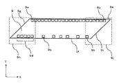
センサチップ9は、図5に示すように、XY平面方向に延在する板状の受光素子であり、光を電気信号に変換する機能を有する。図5は、実施の形態1に係るセンサチップを表す図である。センサチップ9上には、光を電気信号に変換する画素9aが、X方向すなわち長手方向(「センサチップ9の長手方向」は、イメージセンサの主走査方向に相当する)にライン状に配置されている。ライン状に配置された画素9aは少なくとも1ラインが配置され、必要に応じてY方向に複数ラインが並行に配置される。実施の形態1では、簡略化のため、主走査方向に細長い線上の外形だけを図示する。なお、ライン状の画素9aからY方向すなわち短手方向(「センサチップ9の短手方向」は、イメージセンサの副走査方向に相当する)に離間した位置に、画素9aで受光した光を電気信号に変換した信号をセンサチップ9の外部へと取り出す電気接続パッド9bが、複数形成されている。
As shown in FIG. 5, the
センサ基板10およびセンサ基板10を固定するセンサプレート11については、図6、図7、図8及び図11も用いて詳細に説明する。
The
センサ基板10は、XY平面方向に延在する板状の回路基板である。センサ基板10は、センサチップ実装面10aと、X方向側の両端部がX方向に突き出した凸形状部10bと、位置決め穴10cと、コネクタ10dとを備える。センサチップ実装面10aは、X方向に延在する矩形状の領域であり、この領域内に、センサチップ9がX方向にライン上に複数配置される。センサチップ9は、センサチップ実装面10aに接着、はんだ付けなどで実装される。センサチップ9のラインは少なくとも1ラインが配置され、必要に応じて複数ラインがY方向に隣接してX方向に並行に配置される。凸形状部10bは、センサチップ実装面10aに含まれ、X方向の端部に位置する。凸形状部10bは、センサ基板10同士の隣接面に設けるものである。なお、最も外側に位置するセンサ基板10の外側端部は、凸形状でなくとも良い。位置決め穴10cは、センサチップ実装面10aと凸形状部10bとの以外の面に設けられる。位置決め穴10cは、センサ基板10をセンサプレート11上に固定するためのものであるため、少なくとも2つは設けるのが望ましい。コネクタ10dは、センサ基板10のセンサチップ実装面10aの裏面側に実装される、電力供給、駆動制御及び画像情報引き出しのためのコネクタである。なお、センサチップ9が配置(実装)されたセンサ基板10の態様を、センサ基板体とも称する。
The
センサプレート11は、XY平面方向に延在するアルミニウム等の金属、セラミック、ガラスなどの剛性のある板材で、複数のセンサ基板10を実装(固定)するものである。センサプレート11は、位置決め穴11bと固定穴11aを備える。位置決め穴11bは、センサ基板10の位置決め穴10cに対応した大きさと位置関係を持つ。センサ基板10は、X方向にライン上に複数配置(実装)される。センサ基板10は、センサプレート11に接着、はんだ付けなどで実装(固定)される。センサ基板10のラインは少なくとも1ラインが配置され、必要に応じて複数ラインがY方向に隣接してX方向に並行に配置される。
The
なお、センサ基板10が実装(固定)された状態のセンサプレート11の態様を、受光ユニットとも称する。すなわち、実施の形態1に係る受光ユニットは、センサ基板10が実装(固定)された状態のセンサプレート11である。言い換えると、受光ユニットは、センサチップ9が実装されたセンサ基板10(センサ基板体)とセンサプレート11とを備える。
In addition, the aspect of the
ネジ12は、センサ基板10とセンサプレート11と筐体7を固定する。なお、位置決め穴10c、位置決め穴11bと、ネジ12の本数はイメージセンサの大きさに合わせて適切に変更する事は言うまでもない。
The screw 12 fixes the
透明板13は、ガラスや透明な樹脂で成形されたXY平面方向に延在する板状の透明体であり、筐体7の開口部分に固定される。この透明板13の上を原稿や紙幣などの読取対象物がY方向に搬送されるため、透明板13の表面は滑らかである事が望ましい。なお、透明板13は、実施の形態1に係るイメージセンサが搭載されるコピー機や複合機などの画像読取装置側に搭載されており、イメージセンサ側には搭載されないこともある。
The
導光体保持部材14は、導光体1の側面形状に沿った曲面と筐体7の内部面に沿った平面を持つX方向に延在する板材であり、導光体1と組み合わせた上で筐体7に収納するものである。
The light
次に、実施の形態1に係るイメージセンサの動作を説明する。 Next, the operation of the image sensor according to the first embodiment will be described.
光源2は、外部から印加された電力を光に変えて発光する。光源2からの発光は、対向する導光体1の長手方向の端部から導光体1の内部に入射し、導光体1の内部を長手方向に導光する。すなわち、光源2からの発光は、導光体1の壁面において反射を繰り返して長手方向に進む。導光体1の長手方向に沿って形成された白色の印刷パターン又は凹凸形状の散乱領域により、導光体1の内部を導光された光は、導光体1からライン状の光として導光体1の側面から出射される。導光体1から出射した光は、読取対象物の表面で反射し、その反射光の一部が結像素子8でセンサチップ9上に結像される。センサチップ9は結像された光を光電変換し、光電変換した電気信号を画像信号としてコネクタを介して外部に出力する。
The light source 2 emits light by changing externally applied electric power to light. Light emitted from the light source 2 is incident on the inside of the
次に、実施の形態1に係るイメージセンサの製造方法について示す。各工程の説明は、実施の形態1に係るイメージセンサの主走査方向における対称性及び副走査方向における対称性から、一部の説明は、片側の構成要素を用いて説明する。
Next, a method for manufacturing the image sensor according to
イメージセンサの製造方法の工程の基本構成は、照明装置組立工程、結像素子配設工程、照明装置載置工程、センサ(受光部)配列工程、センサ基板配列工程及びセンサ載置工程である。これらの工程のうち、照明装置組立工程は、照明装置載置工程の前に行う必要があり、センサ配列工程及びセンサ基板配列工程は、センサ載置工程の前に行う必要がある。また、結像素子配設工程は、結像素子8を照明装置載置工程の後に取り付けることが困難である場合は、照明装置載置工程の前に行う必要がある。それぞれの工程に関して以降で説明する。
The basic configuration of the process of the image sensor manufacturing method includes an illumination device assembly process, an imaging element arrangement process, an illumination apparatus placement process, a sensor (light receiving unit) arrangement process, a sensor substrate arrangement process, and a sensor placement process. Among these processes, the lighting device assembly process needs to be performed before the lighting device placement process, and the sensor array process and the sensor substrate array process need to be performed before the sensor placement process. Further, when it is difficult to attach the
図1から図3を用いて、照明装置組立工程および結像素子配設工程を説明する。照明装置組立工程は、導光体1の長手方向の端部をホルダ6の挿入孔部に挿入してホルダ6に固定する。また、導光体保持部材14を導光体1の曲面に沿わせる形で添える。ホルダ6の導光体1の挿入側と反対側に、光源基板3と放熱シート4と放熱板5が装着されている。光源基板3は、光源2が導光体1の長手方向の端面に対向し、導光体1の長手方向の端部と光源2とはホルダ6を介して適切な距離を取り対向するように固定される。放熱シート4は、光源基板3の光源2の固定面の裏面に取り付け、放熱板5は放熱シート4の光源基板3の取り付け面の裏面に取り付ける。ホルダ6に設けられている保持部で、光源基板3及び放熱シート4および放熱板5を一体で係合することによりX方向の密着性を高め、放熱性を向上させる。このように、ホルダ6を基準に導光体1、光源基板3、放熱シート4及び放熱板5を組み立てられるので、ホルダ6のみで容易に精度良く光軸が合う照明装置が得られる。導光体保持部材14は長く細い棒材である導光体1のソリや自重によるたわみを抑制し、導光体1と筐体7の距離を適切に保つ。導光体1、光源2、光源基板3、放熱シート4、放熱板5、ホルダ6、および導光体保持部材14、で照明装置101を構成している。
The illumination device assembling process and the imaging element arranging process will be described with reference to FIGS. In the lighting device assembling step, the end of the
結像素子配設工程は、筐体7のスリット部分(X方向に延在した開口)に結像素子8を固定する工程である。なお、結像素子8の焦点は、Z方向に結像素子8の両側に存在するが、一方の片側の焦点を後ほど組み上げるセンサチップ9に、他方の片側の焦点を読取対象物搬送面に合わせて接着剤やテープを用いて固定する。結像素子8のX方向及びY方向の位置決めは、スリットにより決定するか、筐体7に調整機構を別途設けて決定する。
The imaging element disposing step is a step of fixing the
図4を用いて、照明装置載置工程を説明する。照明装置載置工程は、筐体7のX方向端部に設けられた位置決め面を基準に、照明装置101のホルダ6と導光体保持部材14を載置して、筐体7に取付ける。図4は、結像素子配設工程の後に、照明装置載置工程を行う場合を示した図である。厳密には、図4は照明装置101を筐体7に取り付ける直前の状態を示している。
The lighting device placement process will be described with reference to FIG. In the lighting device mounting step, the
図5及び図6を用いて、センサ配列工程を説明する。センサ配列工程は、センサチップ9をセンサ基板10にX方向に実装するものである。図6に示すように、センサ基板10上で、センサチップ9は、X方向の端部を接触させずに、隣接させて配列される。センサ基板10の最端部に位置するセンサチップ9は、センサチップ実装面10aに対して、少なくとも電気接続パッド9bがある部分はセンサチップ実装面10a上に配置し、電気接続パッド9bがないセンサチップ9の最端部をX方向に飛び出した形で実装する。つまり、図5に示すセンサチップ9において、+X方向の最端部の電気接続パッド9bと+X方向のセンサチップ9のチップ端との距離をbとする。また、図5に示すセンサチップ9において、−X方向の最端部の電気接続パッド9bと−X方向のセンサチップ9のチップ端との距離をaとする。このセンサチップ9をセンサ基板10のセンサチップ実装面10aに実装するとき、+X方向の最端部のセンサチップ9は、センサ基板10の+X方向の最端部(+X方向の凸形状部10bの最端部)から、長さbだけ突出してセンサチップ実装面10aに実装する。また、このセンサチップ9をセンサ基板10のセンサチップ実装面10aに実装するとき、−X方向の最端部のセンサチップ9は、センサ基板10の−X方向の最端部(−X方向の凸形状部10bの最端部)から、長さaだけ突出してセンサチップ実装面10aに実装する。これにより、センサチップ9のX方向の端部の電気接続パッド9bは、凸形状部10bを含むセンサ基板10のセンサチップ実装面10a内に配置され、電気接続パッド9bはセンサ基板10と金ワイヤなどで電気的に接続できる。電気接続パッド9bとセンサ基板10を金ワイヤなどで電気的に接続する。
The sensor arrangement process will be described with reference to FIGS. In the sensor arrangement process, the
なお、センサチップ9が実装されたセンサ基板10の態様を、センサ基板体とも称する。
In addition, the aspect of the
ここで、センサチップ9がセンサ基板10のX方向の最端部(X方向の凸形状部10bの最端部)から突出して、センサ基板10に実装される理由を説明する。センサチップ9がセンサ基板10の内部に実装されていると、後述する、センサ基板10をセンサプレート11にX方向に配列するときに、隣接するセンサ基板10のX方向端部に実装されたセンサチップ9同士の間隔が開いてしまい、画素欠落が発生するためである。そこでセンサチップ9がセンサ基板10のX方向の最端部(X方向の凸形状部10bの最端部)から突出していると、後述する、センサ基板10をセンサプレート11にX方向に配列するときに、センサチップ9同士が接触しない範囲で近接して配置されるので、画素欠落が発生しない、若しくは画素欠落が発生しても欠落画素を少なくできる効果があるためである。
Here, the reason why the
また、センサチップ9のセンサ基板10のX方向の最端部(X方向の凸形状部10bの最端部)からの突出長さは、センサチップ9のX方向の端部に最も近い電気接続パッド9bとセンサチップ9の端部までの、一部の画素9aの数の分の長さである。加えて、センサチップ9の大半の部分は、センサ基板10に固定されているため、イメージセンサに外力が加わっても、センサチップ9が破損することのない、外力に強いイメージセンサが得られる。
Further, the protruding length of the
図7及び図8を用いて、センサチップ9が実装されたセンサ基板10を、センサプレート11へ配列するセンサ基板配列工程を説明する。センサ基板10は、センサプレート11にX方向にライン状に複数配列する。このとき、隣接するセンサ基板10のX方向の端部に実装されたセンサチップ9の、センサ基板10の凸形状部10bから突出した部分が、互いに接触することなく隣接するようにセンサ基板10を位置決めして、センサ基板10をセンサプレート11に配列し実装(固定)する。センサプレート11におけるセンサ基板10の位置決めは、凸形状部10bを用いて実施する。また、隣接するセンサ基板10に実装されたセンサチップ9の画素9aの列は、同じラインとなるように実装する。
A sensor substrate arranging step for arranging the
図9A、図9B、図9Cを用いて、センサ基板10をセンサプレート11へ配列するセンサ基板配列工程を詳細に説明する。例えば、図9Aに示すように、センサプレート11に、センサ基板10の位置決め用のマーキングをX方向(X方向マーキング11e、11g、11i、11k)およびY方向(Y方向マーキング11f、11h、11j、11L)に実施しておく。図9Cに示すように、センサ基板10の凸形状部10bのX方向に延在する辺10e、10g、10i、10k(図9B参照)を、センサプレート11のX方向マーキング11e、11g、11i、11kにそれぞれ一致させる。さらに、センサ基板10の凸形状部10bの凸端ではない方のY方向に延在する辺10f、10h、10j、10L(図9B参照)を、Y方向マーキング11f、11h、11j、11Lにそれぞれ一致させる。結果、センサ基板10をセンサプレート11に精度良く配列することができる。これにより、センサ基板10のX方向の端部に実装されたセンサチップ9も、隣接するセンサチップ9同士が精度良く配列されることになる。
9A, 9B, and 9C, the sensor substrate arranging step for arranging the
図10A、図10B、図10Cを用いて、センサ基板10をセンサプレート11へ配列するセンサ基板配列工程の他の例を詳細に説明する。なお、他の例のセンサ基板10の位置決めとして、図10Aに示すように、センサプレート11において、センサ基板10の凸形状部10bの根元の部分のセンサ基板10のX方向の辺とY方向の辺との交点に対応する位置に、点マークもしくは位置決めピン11m、11n、11p、11qを設けておく。図10Cに示すように、この点マークもしくは位置決めピン11m、11n、11p、11qに、センサ基板10の凸形状部10bの根元の部分のセンサ基板10のX方向の辺とY方向の辺との交点10m、10n、10p、10q(図10B参照)を、一致させて、センサ基板10を配列する。結果、センサ基板10をセンサプレート11に精度良く配列することができる。加えて、位置決め穴10cと位置決め穴11bを合わせるように配列する事で、隣接するセンサ基板10、つまりはセンサチップ9同士の距離が適切に保たれる。なお、位置決めピンは、センサ基板10をセンサプレート11に配列した後、残しておいても良いし、除去しても良い。
Another example of the sensor substrate arranging step for arranging the
センサプレート11にセンサ基板10を配列するとき、隣接するセンサ基板10同士のX方向の端部に実装された、向き合っているセンサチップ9同士の間隔が以下の状態となるように、センサ基板10をセンサプレート11に配列する。第1に、センサチップ9に形成された画素9a同士の中心のX方向の間隔(画素ピッチという)の1/2の長さよりも、センサチップ9のX方向の端部に形成された画素9aの中心とセンサチップ9のX方向の端部との長さが小さい場合の配列は、次の通りである。向き合っているセンサチップ9の端部の画素9a同士の間隔が画素ピッチに等しくなるように、センサプレート11にセンサ基板10を配列する。第2に、センサチップ9に形成された画素9aの中心のX方向の間隔(画素ピッチという)の1/2の長さよりも、センサチップ9のX方向の端部に形成された画素9aの中心とセンサチップ9のX方向の端部との長さが長い場合の配列は、次の通りである。向き合っているセンサチップ9の端部の画素9a同士の間隔が、向き合っているセンサチップ9同士が接触しない範囲で、向き合っているセンサチップ9の端部の画素9a同士の間隔が2以上の最も小さい整数倍の画素ピッチとなるように、センサプレート11にセンサ基板10を配列する。すなわち、向き合っているセンサチップ9同士は、向き合っているセンサチップ9の端部の画素9a同士の間隔が画素ピッチのN倍(Nは整数)の距離を取る。このとき、向き合っているセンサチップ9同士が接触しない範囲で、Nは1若しくはできるだけ小さい数にして画素欠落を減らし、センサチップ9間の画質を落とさないようにする。例として、解像度が600dpiの場合、センサチップ9の画素9aの画素ピッチは42.3μmとなるので、向き合っているセンサチップ9の端部の画素9a同士の間隔は最小で42.3μmとなる。
When the
なお、センサ基板10が実装(固定)されたセンサプレート11の態様を、受光ユニットとも称するので、センサ配列工程とセンサ基板配列工程とで受光ユニット組立工程を構成している。
The mode of the
センサ載置工程は、図2に示すように、筐体7の照明装置を載置した側のZ方向の裏面側に筐体7の内側にセンサチップ9が納められ、かつ、結像素子8の光軸上にセンサチップ9がX方向に並ぶようにセンサプレート11をネジ12で筐体に固定する。
As shown in FIG. 2, in the sensor mounting process, a
図12は、実施の形態1に係るイメージセンサに透明板13を設ける場合に、少なくとも、照明装置組立工程、結像素子配設工程、照明装置載置工程の後に行う必要がある透明板載置工程を示すものである。透明板載置工程は、筐体7へ透明板13を載置するものである。透明板13の載置面は、透明板13の外形と一致することが望ましい。筐体7の一方の開口の縁部に透明板13が保持できる形状の階段状の段差を形成するか、筐体7の最上部を用いて、透明板13を接着などで固定する。
FIG. 12 shows that when the
このように、実施の形態1に係るイメージセンサでは、センサチップ9を、センサチップ9の長手方向端部から長手方向端部に最も近い電気接続パッド9bまでの長さだけ、センサ基板10の長手方向端部の凸形状部10bから長手方向に突出させる。次に、凸形状部10bを用いてセンサ基板10の位置決めを行いつつ、センサ基板10から突出したセンサチップ9同士を、近接して隣接させて、センサ基板10を長手方向にライン状に配設している。このため、イメージセンサの受光ユニットは、組立性が良く、外力に強い構造が得られる効果がある。
As described above, in the image sensor according to the first embodiment, the
実施の形態1では、図2及び図3に示すように光源2及び導光体1で構成された照明装置と受光ユニットが同じ筐体7に収納され、受光ユニットは照明装置からの光が読取対象物で反射した反射光を受光する態様を説明した。これに代えて、光源2及び導光体1で構成された照明装置を筐体7から取り出し、透明板13を介して受光ユニットとは反対側に設置し、透明板13と照明装置との間に読取対象物が搬送される構成としても良い。この場合、受光ユニットは、照明装置からの光が読取対象物を透過した透過光を受光することになるが、その作用効果は、反射光を受光する図2及び図3の態様と同じである。
In the first embodiment, as shown in FIGS. 2 and 3, the illumination device composed of the light source 2 and the
実施の形態2.
図13、図14を用いて、この発明の実施の形態2に係る受光ユニットについて説明する。図13、図14において、図1から図12と同一若しくは同等の構成要素には同一符号を付し、その説明を省略する。実施の形態2において、図中で、それぞれが直交してX、Y、Zと記されている3軸の定義は、実施の形態1と同じである。Embodiment 2. FIG.
A light receiving unit according to Embodiment 2 of the present invention will be described with reference to FIGS. In FIG. 13 and FIG. 14, the same reference numerals are given to the same or equivalent components as in FIG. 1 to FIG. In the second embodiment, the definitions of the three axes that are orthogonally marked as X, Y, and Z in the drawing are the same as those in the first embodiment.
実施の形態1では、受光ユニットは、向き合っているセンサチップ9の端部の画素9a同士の間隔が、向き合っているセンサチップ9同士が接触しない範囲で、センサプレート11にセンサ基板10を配列している。このため、向き合っているセンサチップ9同士において、隙間16が発生しており、この隙間16の箇所には画素9aが存在しないため、画素の欠落(欠落画素)9cが発生する。なお、向き合っているそれぞれのセンサチップ9の画素9aの列が、同じライン上に配置されるように、それぞれのセンサチップ9は実装されている。
In the first embodiment, the light receiving unit arranges the
実施の形態2に係る受光ユニットは、実施の形態1に係る受光ユニットに加えて、第2の画素109aを形成した補間用センサチップ109が配置されている。補間用センサチップ109は、補間用センサ基板110に接着、はんだ付けなどによって、実装されている。この補間用センサ基板110がセンサプレート11に接着、はんだ付けなどによって、実装(固定)されている。補間用センサチップ109は、第2の画素109aで受光した光を光電変換した電気信号を、外部に出力する電気接続パッド109bを備えている。センサ基板10及び補間用センサ基板110は、接着、はんだ付けなどによって、センサプレート11に実装(固定)されているが、図13、図14では、センサプレート11を省略している。
In the light receiving unit according to the second embodiment, in addition to the light receiving unit according to the first embodiment, an
補間用センサチップ109は、向かい合うセンサチップ9の端部に、センサチップ9の短手方向(「センサチップ9の短手方向」は、イメージセンサの副走査方向に相当する)に隣接して、配置されている。補間用センサチップ109は、向かい合うセンサチップ9の両方の端部に隣接して配置されている。補間用センサチップ109は、センサチップ9の長手方向と同じ方向すなわち主走査方向にライン状に複数の第2の画素109aが形成されている。補間用センサチップ109は、第2の画素109aの少なくとも1ラインが、副走査方向にずれて配置されている。また、複数の第2の画素109aは、主走査方向に、それぞれのセンサチップ9の画素9aとオーバラップしている。図14においては、第2の画素109aは6素子が形成されている。第2の画素109aの画素ピッチは、センサチップ9の画素9aの画素ピッチと同じである。
The
図14において、センサチップ9の短手方向に透視したとき、6素子の第2の画素109aの内、ライン方向(センサチップ9の長手方向と同じ方向)の一端側の2素子が、向かい合うセンサチップ9同士において、一方のセンサチップ9の端部に形成された2素子の画素9aとオーバラップしている(図14の破線参照)。また、図14において、センサチップ9の短手方向に透視したとき、6素子の第2の画素109aの内、ライン方向(センサチップ9の長手方向と同じ方向)の他端側の2素子が、向かい合うセンサチップ9同士において、他方のセンサチップ9の端部に形成された2素子の画素9aとオーバラップしている(図14の破線参照)。図14では、オーバラップする第2の画素109aは2素子であったが、最低、1素子がオーバラップすれば良い。
In FIG. 14, when viewed in the short direction of the
したがって、6素子の第2の画素109aの内、ライン方向(センサチップ9の長手方向と同じ方向)の両端部の4素子を除いた、ライン方向(センサチップ9の長手方向と同じ方向)の中央部にある2素子の第2の画素109aが、欠落画素9cを補間する補間画素となる。
Therefore, among the six elements of the
センサチップ9を含む受光ユニットは、使用温度によって、熱膨張係数により熱伸縮が発生する。そのため、向かい合うセンサチップ9の端部同士の隙間16の間隔は、使用温度によって変化する。そこで、補間用センサチップ109は、向かい合うセンサチップ9の端部同士の隙間16の間隔が、使用する温度範囲内で最も大きくなった場合においても、欠落画素9cを補間できる数の第2の画素109aが形成されている。
The light receiving unit including the
つまり、補間用センサチップ109は、第2の画素109aを、ライン状に形成された第2の画素109aの列の一端側の第2の画素109aから他端側の第2の画素109aまでの距離が、センサチップ9が使用する温度範囲内で最も開いたときの、向かい合うセンサチップ9の端部に形成された画素9a同士の間隔以上として形成している。
That is, the
例を示して説明する。センサプレート11をアルミニウム、センサ基板10をガラスエポキシ基板、センサチップ9をシリコン半導体基板で構成した例を示す。+25度の温度において、向かい合うセンサチップ9同士の端部の隙間16の間隔は50μmとする。この状態でシミュレーションしたところ、+80度の温度では、隙間16の間隔は107μmとなり、−20度の温度では、隙間16の間隔は3μmとの結果を得た。
An example will be described. An example is shown in which the
解像度が600dpiの場合、センサチップ9の画素9aの画素ピッチは42.3μmであるので、25度の温度での欠落画素9cは2画素となる。よって、補間用センサチップ109の第2の画素109aは4画素で良いことになる。
When the resolution is 600 dpi, the pixel pitch of the
ところで、+80度の温度では、向かい合うセンサチップ9同士の端部の隙間16の間隔は107μmとなるので、欠落画素9cは3画素となる。よって、補間用センサチップ109の第2の画素109aは、最低でも5画素必要となる。
By the way, at the temperature of +80 degrees, since the
よって、実施の形態2の上述の例では、向かい合うセンサチップ9の端部同士の隙間16の間隔が、使用する温度範囲内(−20度から+80度)で最も大きくなった107μmの場合においても、欠落画素9cを補間できる最低でも5画素の第2の画素109aが、補間用センサチップ109に形成されている。このように、実施の形態2においては、使用する温度範囲における受光ユニットの寸法変化も吸収して、欠落画素を補間することができる。
Therefore, in the above-described example of the second embodiment, even when the
実施の形態3.
図15から図17を用いて、この発明の実施の形態2に係る受光ユニットについて説明する。図15から図17において、図1から図12と同一若しくは同等の構成要素には同一符号を付し、その説明を省略する。実施の形態3において、図中で、それぞれが直交してX、Y、Zと記されている3軸の定義は、実施の形態1と同じである。
A light receiving unit according to Embodiment 2 of the present invention will be described with reference to FIGS. 15 to 17. 15 to FIG. 17, the same or equivalent components as those in FIG. 1 to FIG. In the third embodiment, the definitions of the three axes that are orthogonally marked as X, Y, and Z in the drawing are the same as those in the first embodiment.
実施の形態1では、受光ユニットは、向き合っているセンサチップ9の端部の画素9a同士の間隔が、向き合っているセンサチップ9同士が接触しない範囲で、センサプレート11にセンサ基板10を配列している。このため、向き合っているセンサチップ9同士において、隙間16が発生しており、この隙間16の箇所には画素9aが存在しないため、画素の欠落(欠落画素)9cが発生する。なお、向き合っているそれぞれのセンサチップ9の画素9aが、同じライン上に配置されるように、それぞれのセンサチップ9は実装されている。
In the first embodiment, the light receiving unit arranges the
実施の形態3に係る受光ユニットは、センサチップ9が平行四辺形の形状をしている。平行四辺形の長手方向の両端部に形成された傾斜辺が、お互い向かい合うようにしてセンサチップ9が配置されている。センサチップ9はセンサ基板10に接着、はんだ付けなどで、実装されている。このセンサ基板10はセンサプレート11に接着、はんだ付けなどで、実装(固定)されている。なお、図15では、センサプレート11を省略している。
In the light receiving unit according to
具体的には、センサチップ9の長手方向の一方の端部は、センサチップ9の長手方向の外側方向へ向かうに従い、センサチップ9の長手方向の一方の辺9eから長手方向の他方の辺9fへと向かう傾斜形状の第1の傾斜辺9gと長手方向の他方の辺9fとで構成される第1の傾斜部9hを有する。センサチップ9の長手方向の他方の端部は、センサチップ9の長手方向の外側方向へ向かうに従い、センサチップ9の長手方向の他方の辺9fから長手方向の一方の辺9eへと向かう傾斜形状の第2の傾斜辺9iと長手方向の一方の辺9eとで構成される第2の傾斜部9jを有する。
Specifically, one end of the
向き合っているセンサチップ9の端部同士は、一方のセンサチップ9の第1の傾斜辺9gと他方のセンサチップ9の第2の傾斜辺9iとが、センサチップ9の長手方向及び長手方向に直交する短手方向に透視したとき、オーバラップして配置されている。センサチップ9は、一方の辺9e側に長手方向にライン状に複数の画素9aが形成されている。なお、向き合っているそれぞれのセンサチップ9の画素9aの列が、同じライン上に配置されるように、それぞれのセンサチップ9は実装されている。
The ends of the
センサチップ9は、第1の傾斜部9hの他方の辺9f側に長手方向にライン状に複数の第2の画素9dが形成されている。ライン状の複数の第2の画素9dは、ライン状の複数の画素9aから少なくとも副走査方向に1ラインずれて形成されている。第2の画素9dの画素ピッチは画素9aの画素ピッチと同じである。ライン状に形成された複数の第2の画素9dで構成される第2の画素列の、第1の傾斜辺9g側とは反対側すなわち第2の傾斜辺9i側の端部に位置する第2の画素9dは、センサチップ9の短手方向に透視したとき、画素9aとオーバラップする位置に形成されている。ライン状に形成された複数の第2の画素9dで構成される第2の補間画素列の、第1の傾斜辺9g側の端部に位置する第2の画素9dは、センサチップ9の短手方向に透視したとき、向かい合う反対側のセンサチップ9の第2の傾斜辺9i側の画素9aとオーバラップするように、向かい合うセンサチップ9同士が実装されている。
In the
図17においては、第2の画素9dは5素子が形成されている。図17において、センサチップ9の短手方向に透視したとき、5素子の第2の画素9dの内、ライン方向(センサチップ9の長手方向と同じ方向)の第1の傾斜辺9gとは反対側すなわち第2の傾斜辺9i側の端部に位置する1素子が、第2の画素9dが形成されたセンサチップ9に形成された1素子の画素9aとオーバラップしている。また、図17において、センサチップ9の短手方向に透視したとき、5素子の第2の画素9dの内、ライン方向(センサチップ9の長手方向と同じ方向)の第1の傾斜辺9g側の端部に位置する1素子が、向かい合う反対側のセンサチップ9の第2の傾斜辺9i側の端部に形成された1素子の画素9aとオーバラップしている。図17では、オーバラップする第2の画素9dは1素子であったが、2素子以上がオーバラップしても良い。
In FIG. 17, the
したがって、5素子の第2の画素9dの内、ライン方向(センサチップ9の長手方向と同じ方向)の両端部の2素子を除いた、ライン方向(センサチップ9の長手方向と同じ方向)の中央部にある3素子の第2の画素9dが、欠落画素9cを補間する補間画素となる。
Therefore, in the
センサチップ9を含む受光ユニットは、使用温度によって、熱膨張係数により熱伸縮が発生する。そのため、向かい合うセンサチップ9の端部同士の隙間16の間隔は、使用温度によって変化する。そこで、センサチップ9には、向かい合うセンサチップ9の端部同士の隙間16の間隔が、使用する温度範囲内で最も大きくなった場合においても、欠落画素9cを補間できる数の第2の画素9dが形成されている。
The light receiving unit including the
つまり、センサチップ9は、第2の画素9dを、ライン状に形成された第2の画素9dの列の一端側の第2の画素9dから他端側の第2の画素9dまでの距離が、センサチップ9が使用する温度範囲内で最も開いたときの、向かい合うセンサチップ9の端部に形成された画素9a同士の間隔以上として形成している。
That is, in the
例を示して説明する。センサプレート11をアルミニウム、センサ基板10をガラスエポキシ基板、センサチップ9をシリコン半導体基板で構成した例を示す。+25度の温度において、向かい合うセンサチップ9同士の端部の隙間16の間隔は50μmとする。この状態でシミュレーションしたところ、+80度の温度では、隙間16の間隔は107μmとなり、−20度の温度では、隙間16の間隔は3μmとの結果を得た。
An example will be described. An example is shown in which the
解像度が600dpiの場合、センサチップ9の画素9aの画素ピッチは42.3μmであるので、25度の温度での欠落画素9cは、センサチップ9が平行四辺形形状であるため3画素となる。よって、センサチップ9の第2の画素9dは5画素で良いことになる。
When the resolution is 600 dpi, the pixel pitch of the
ところで、+80度の温度では、向かい合うセンサチップ9同士の端部の隙間16の間隔は107μmとなるので、欠落画素9cは4画素となる。よって、センサチップ9の第2の画素9dは、最低でも6画素必要となる。
By the way, at the temperature of +80 degrees, the
よって、実施の形態3の上述の例では、向かい合うセンサチップ9の端部同士の隙間16の間隔が、使用する温度範囲内(−20度から+80度)で最も大きくなった107μmの場合においても、欠落画素9cを補間できる最低でも6画素の第2の画素9dが、センサチップ9に形成されている。このように、実施の形態3においては、使用する温度範囲における受光ユニットの寸法変化も吸収して、欠落画素を補間することができる。
Therefore, in the above-described example of the third embodiment, even when the
1 導光体、
2 光源、
3 光源基板、
4 放熱シート、
5 放熱板、
6 ホルダ、
7 筐体、
8 結像素子、
9 センサチップ、
9a 画素、
9b 電気接続パッド、
9c 欠落画素、
9d 第2の画素、
9e 一方の辺、
9f 他方の辺、
9g 第1の傾斜辺、
9h 第1の傾斜部、
9i 第2の傾斜辺、
9j 第2の傾斜部、
10 センサ基板(センサ基板体)、
10a センサチップ実装面、
10b 凸形状部、
10c 位置決め穴、
10d コネクタ、
10e 辺、
10f 辺、
10g 辺、
10h 辺、
10i 辺、
10j 辺、
10k 辺、
10L 辺、
10m 交点、
10n 交点、
10p 交点、
11q 交点、
11 センサプレート、
11a 固定穴、
11b 位置決め穴、
11e マーキング、
11f マーキング、
11g マーキング、
11h マーキング、
11i マーキング、
11j マーキング、
11k マーキング、
11L マーキング、
11m 点マークもしくは位置決めピン、
11n 点マークもしくは位置決めピン、
11p 点マークもしくは位置決めピン、
11q 点マークもしくは位置決めピン、
12 ネジ、
13 透明板、
14 導光体保持部材、
16 隙間、
101 照明装置、
109 補間用センサチップ、
109a 第2の画素、
109b 電気接続パッド、
110 補間用センサ基板。1 light guide,
2 light source,
3 Light source board,
4 Heat dissipation sheet,
5 Heat sink,
6 holder,
7 housing,
8 Imaging element,
9 Sensor chip,
9a pixels,
9b Electrical connection pad,
9c missing pixels,
9d second pixel,
9e one side,
9f the other side,
9g first inclined side,
9h 1st inclined part,
9i second inclined side,
9j second inclined part,
10 sensor substrate (sensor substrate body),
10a Sensor chip mounting surface,
10b convex part,
10c positioning hole,
10d connector,
10e side,
10f side,
10g side,
10h side,
10i side,
10j sides,
10k side,
10L side,
10m intersection,
10n intersection,
10p intersection,
11q intersection,
11 Sensor plate,
11a fixing hole,
11b Positioning hole,
11e marking,
11f marking,
11g marking,
11h marking,
11i marking,
11j marking,
11k marking,
11L marking,
11m point mark or positioning pin,
11n point mark or positioning pin,
11p point mark or positioning pin,
11q point mark or positioning pin,
12 screws,
13 Transparent plate,
14 light guide holding member,
16 Clearance,
101 lighting device,
109 sensor chip for interpolation,
109a second pixel,
109b electrical connection pads,
110 Interpolation sensor board.
Claims (9)
複数の前記センサ基板体を前記長手方向にライン状に配列して実装したセンサプレートと、を備え、
前記センサチップは前記長手方向にライン状に形成された複数の画素を有し、
前記センサ基板体の前記長手方向の端部は、前記センサチップが前記センサ基板の前記長手方向の端部から前記長手方向へ前記センサ基板の外側へ突出し、
隣接する前記センサ基板体の前記長手方向の端部に実装された、向かい合う前記センサチップ同士は、前記向かい合う前記センサチップの端部同士が所定の間隔で離間し、
前記センサ基板は、前記長手方向の端部に前記長手方向に突出した凸形状部を有し、
前記センサチップは、前記凸形状部に実装され、
前記センサ基板体は、前記センサ基板の凸形状部を前記センサプレートに設けられた位置合わせ部に位置合わせして、前記センサプレートに実装した受光ユニット。 A plurality of sensor chips arranged in a line in the longitudinal direction of the sensor substrate and mounted on the sensor substrate; and
A plurality of sensor substrate bodies arranged in a line in the longitudinal direction and mounted, and a sensor plate,
The sensor chip has a plurality of pixels formed in a line shape in the longitudinal direction,
The end of the sensor substrate body in the longitudinal direction is such that the sensor chip protrudes outward from the sensor substrate in the longitudinal direction from the end of the sensor substrate in the longitudinal direction.
The sensor chips facing each other mounted on the end portions in the longitudinal direction of the adjacent sensor substrate bodies are separated from each other by a predetermined interval between the end portions of the sensor chips facing each other.
The sensor substrate has a convex portion protruding in the longitudinal direction at an end in the longitudinal direction,
The sensor chip is mounted on the convex portion,
The sensor substrate body is a light receiving unit mounted on the sensor plate by aligning a convex portion of the sensor substrate with an alignment portion provided on the sensor plate.
複数の前記センサ基板体を前記長手方向にライン状に配列して実装したセンサプレートと、を備え、
前記センサチップは前記長手方向にライン状に形成された複数の画素を有し、
前記センサ基板体の前記長手方向の端部は、前記センサチップが前記センサ基板の前記長手方向の端部から前記長手方向へ前記センサ基板の外側へ突出し、
隣接する前記センサ基板体の前記長手方向の端部に実装された、向かい合う前記センサチップ同士は、前記向かい合う前記センサチップの端部同士が所定の間隔で離間し、
前記センサ基板は、前記長手方向の端部に前記長手方向に突出した凸形状部を有し、
前記センサチップは、前記凸形状部に実装され、
前記センサ基板体は、前記センサ基板の凸形状部を前記センサプレートに設けられた位置合わせ部に位置合わせして、前記センサプレートに実装され、
前記センサチップは、複数の前記画素とは短手方向の異なる位置に、前記長手方向に形成した複数の電気接続パッドを備え、
前記センサチップが前記センサ基板体の端部から前記長手方向へ前記センサ基板体の外側へ突出している前記センサチップの突出長さは、前記センサチップの長手方向の端部に最も近い前記電気接続パッドと前記センサチップの長手方向の端部との距離以下である受光ユニット。 A plurality of sensor chips arranged in a line in the longitudinal direction of the sensor substrate and mounted on the sensor substrate; and
A plurality of sensor substrate bodies arranged in a line in the longitudinal direction and mounted, and a sensor plate,
The sensor chip has a plurality of pixels formed in a line shape in the longitudinal direction,
The end of the sensor substrate body in the longitudinal direction is such that the sensor chip protrudes outward from the sensor substrate in the longitudinal direction from the end of the sensor substrate in the longitudinal direction.
The sensor chips facing each other mounted on the end portions in the longitudinal direction of the adjacent sensor substrate bodies are separated from each other by a predetermined interval between the end portions of the sensor chips facing each other.
The sensor substrate has a convex portion protruding in the longitudinal direction at an end in the longitudinal direction,
The sensor chip is mounted on the convex portion,
The sensor substrate body is mounted on the sensor plate by aligning a convex portion of the sensor substrate with an alignment portion provided on the sensor plate,
The sensor chip includes a plurality of electrical connection pads formed in the longitudinal direction at positions different from the plurality of pixels in the short-side direction,
The protruding length of the sensor chip in which the sensor chip protrudes from the end portion of the sensor substrate body in the longitudinal direction to the outside of the sensor substrate body is closest to the longitudinal end portion of the sensor chip. A light receiving unit that is equal to or shorter than a distance between a pad and a longitudinal end portion of the sensor chip.
複数の前記センサ基板体を前記長手方向にライン状に配列して実装したセンサプレートと、を備え、
前記センサチップは前記長手方向にライン状に形成された複数の画素を有し、
前記センサ基板体の前記長手方向の端部は、前記センサチップが前記センサ基板の前記長手方向の端部から前記長手方向へ前記センサ基板の外側へ突出し、
隣接する前記センサ基板体の前記長手方向の端部に実装された、向かい合う前記センサチップ同士は、前記向かい合う前記センサチップの端部同士が所定の間隔で離間し、
前記センサ基板は、前記長手方向の端部に前記長手方向に突出した凸形状部を有し、
前記センサチップは、前記凸形状部に実装され、
前記センサ基板体は、前記センサ基板の凸形状部を前記センサプレートに設けられた位置合わせ部に位置合わせして、前記センサプレートに実装され、
前記向かい合う前記センサチップの端部に、前記長手方向に直交する短手方向に隣接して配置された補間用センサチップを備え、
前記補間用センサチップは、前記長手方向にライン状に形成された複数の第2の画素を有し、
前記向かい合う前記センサチップと前記補間用センサチップとを前記短手方向に透視したとき、ライン状に形成された前記第2の画素の列の一端側の前記第2の画素と一方の前記センサチップの端部に形成された前記画素とがオーバラップし、
前記第2の画素の列の他端側の前記第2の画素と他方の前記センサチップの端部に形成された前記画素とがオーバラップしている受光ユニット。 A plurality of sensor chips arranged in a line in the longitudinal direction of the sensor substrate and mounted on the sensor substrate; and
A plurality of sensor substrate bodies arranged in a line in the longitudinal direction and mounted, and a sensor plate,
The sensor chip has a plurality of pixels formed in a line shape in the longitudinal direction,
The end of the sensor substrate body in the longitudinal direction is such that the sensor chip protrudes outward from the sensor substrate in the longitudinal direction from the end of the sensor substrate in the longitudinal direction.
The sensor chips facing each other mounted on the end portions in the longitudinal direction of the adjacent sensor substrate bodies are separated from each other by a predetermined interval between the end portions of the sensor chips facing each other.
The sensor substrate has a convex portion protruding in the longitudinal direction at an end in the longitudinal direction,
The sensor chip is mounted on the convex portion,
The sensor substrate body is mounted on the sensor plate by aligning a convex portion of the sensor substrate with an alignment portion provided on the sensor plate,
An interpolation sensor chip disposed adjacent to the opposite end of the sensor chip in the lateral direction perpendicular to the longitudinal direction;
The interpolation sensor chip has a plurality of second pixels formed in a line shape in the longitudinal direction,
When the sensor chip and the interpolating sensor chip facing each other are seen through in the lateral direction, the second pixel on one end side of the column of the second pixels formed in a line shape and one of the sensor chips Overlap with the pixel formed at the end of
The light receiving unit in which the second pixel on the other end side of the second pixel column overlaps the pixel formed at the end of the other sensor chip.
前記補間用センサチップは、前記長手方向にライン状に形成された複数の第2の画素を有し、
前記向かい合う前記センサチップと前記補間用センサチップとを前記短手方向に透視したとき、ライン状に形成された前記第2の画素の列の一端側の前記第2の画素と一方の前記センサチップの端部に形成された前記画素とがオーバラップし、
前記第2の画素の列の他端側の前記第2の画素と他方の前記センサチップの端部に形成された前記画素とがオーバラップしている請求項2に記載の受光ユニット。 An interpolation sensor chip disposed adjacent to the opposite end of the sensor chip in the lateral direction perpendicular to the longitudinal direction;
The interpolation sensor chip has a plurality of second pixels formed in a line shape in the longitudinal direction,
When the sensor chip and the interpolating sensor chip facing each other are seen through in the lateral direction, the second pixel on one end side of the column of the second pixels formed in a line shape and one of the sensor chips Overlap with the pixel formed at the end of
3. The light receiving unit according to claim 2 , wherein the second pixel on the other end side of the second pixel column overlaps the pixel formed at the end of the other sensor chip.
複数の前記センサ基板体を前記長手方向にライン状に配列して実装したセンサプレートと、を備え、
前記センサチップは前記長手方向にライン状に形成された複数の画素を有し、
前記センサ基板体の前記長手方向の端部は、前記センサチップが前記センサ基板の前記長手方向の端部から前記長手方向へ前記センサ基板の外側へ突出し、
隣接する前記センサ基板体の前記長手方向の端部に実装された、向かい合う前記センサチップ同士は、前記向かい合う前記センサチップの端部同士が所定の間隔で離間し、
前記センサ基板は、前記長手方向の端部に前記長手方向に突出した凸形状部を有し、
前記センサチップは、前記凸形状部に実装され、
前記センサ基板体は、前記センサ基板の凸形状部を前記センサプレートに設けられた位置合わせ部に位置合わせして、前記センサプレートに実装され、
前記センサチップの前記長手方向の一方の端部は、前記センサチップの前記長手方向の外側方向へ向かうに従い、前記センサチップの前記長手方向の一方の辺から前記長手方向の他方の辺へと向かう傾斜形状の第1の傾斜辺を有し、
前記センサチップの前記長手方向の他方の端部は、前記センサチップの前記長手方向の外側方向へ向かうに従い、前記他方の辺から前記一方の辺へと向かう傾斜形状の第2の傾斜辺を有し、
前記向かい合う前記センサチップの端部同士は、一方の前記センサチップの前記第1の傾斜辺と他方の前記センサチップの前記第2の傾斜辺とが、前記長手方向に直交する短手方向に透視したとき、オーバラップして配置されており、
前記センサチップは、前記一方の辺側に前記長手方向にライン状に形成された複数の前記画素と、前記他方の辺側に前記長手方向にライン状に形成された複数の第2の画素を有し、
複数の前記第2の画素の内の前記第2の傾斜辺側の前記第2の画素は、前記短手方向に透視したとき、当該センサチップの前記画素とオーバラップしており、
複数の前記第2の画素の内の前記第1の傾斜辺側の前記第2の画素は、前記短手方向に透視したとき、前記向かい合う前記センサチップの前記画素とオーバラップしている受光ユニット。 A plurality of sensor chips arranged in a line in the longitudinal direction of the sensor substrate and mounted on the sensor substrate; and
A plurality of sensor substrate bodies arranged in a line in the longitudinal direction and mounted, and a sensor plate,
The sensor chip has a plurality of pixels formed in a line shape in the longitudinal direction,
The end of the sensor substrate body in the longitudinal direction is such that the sensor chip protrudes outward from the sensor substrate in the longitudinal direction from the end of the sensor substrate in the longitudinal direction.
The sensor chips facing each other mounted on the end portions in the longitudinal direction of the adjacent sensor substrate bodies are separated from each other by a predetermined interval between the end portions of the sensor chips facing each other.
The sensor substrate has a convex portion protruding in the longitudinal direction at an end in the longitudinal direction,
The sensor chip is mounted on the convex portion,
The sensor substrate body is mounted on the sensor plate by aligning a convex portion of the sensor substrate with an alignment portion provided on the sensor plate,
One end portion of the sensor chip in the longitudinal direction is directed from one side in the longitudinal direction of the sensor chip to the other side in the longitudinal direction as it goes outward in the longitudinal direction of the sensor chip. A first inclined side having an inclined shape;
The other end of the sensor chip in the longitudinal direction has a second inclined side having an inclined shape that extends from the other side to the one side as it goes outward in the longitudinal direction of the sensor chip. And
The ends of the sensor chips facing each other are seen through in a lateral direction in which the first inclined side of one sensor chip and the second inclined side of the other sensor chip are orthogonal to the longitudinal direction. Are placed in an overlapping manner,
The sensor chip includes a plurality of pixels formed in a line in the longitudinal direction on the one side and a plurality of second pixels formed in a line in the longitudinal direction on the other side. Have
The second pixel on the second inclined side side of the plurality of second pixels overlaps with the pixel of the sensor chip when seen through in the lateral direction,
The second pixel on the first inclined side side of the plurality of second pixels overlaps with the pixels of the sensor chip facing each other when viewed in the lateral direction. .
前記センサチップの前記長手方向の他方の端部は、前記センサチップの前記長手方向の外側方向へ向かうに従い、前記他方の辺から前記一方の辺へと向かう傾斜形状の第2の傾斜辺を有し、
前記向かい合う前記センサチップの端部同士は、一方の前記センサチップの前記第1の傾斜辺と他方の前記センサチップの前記第2の傾斜辺とが、前記長手方向に直交する短手方向に透視したとき、オーバラップして配置されており、
前記センサチップは、前記一方の辺側に前記長手方向にライン状に形成された複数の前記画素と、前記他方の辺側に前記長手方向にライン状に形成された複数の第2の画素を有し、
複数の前記第2の画素の内の前記第2の傾斜辺側の前記第2の画素は、前記短手方向に透視したとき、当該センサチップの前記画素とオーバラップしており、
複数の前記第2の画素の内の前記第1の傾斜辺側の前記第2の画素は、前記短手方向に透視したとき、前記向かい合う前記センサチップの前記画素とオーバラップしている請求項2に記載の受光ユニット。 One end portion of the sensor chip in the longitudinal direction is directed from one side in the longitudinal direction of the sensor chip to the other side in the longitudinal direction as it goes outward in the longitudinal direction of the sensor chip. A first inclined side having an inclined shape;
The other end of the sensor chip in the longitudinal direction has a second inclined side having an inclined shape that extends from the other side to the one side as it goes outward in the longitudinal direction of the sensor chip. And
The ends of the sensor chips facing each other are seen through in a lateral direction in which the first inclined side of one sensor chip and the second inclined side of the other sensor chip are orthogonal to the longitudinal direction. Are placed in an overlapping manner,
The sensor chip includes a plurality of pixels formed in a line in the longitudinal direction on the one side and a plurality of second pixels formed in a line in the longitudinal direction on the other side. Have
The second pixel on the second inclined side side of the plurality of second pixels overlaps with the pixel of the sensor chip when seen through in the lateral direction,
The second pixel on the first inclined side side of the plurality of second pixels overlaps with the pixel of the sensor chip facing each other when viewed in the short direction. The light receiving unit according to 2 .
項6または請求項7に記載の受光ユニット。 The distance from the second pixel on one end side to the second pixel on the other end side of the second pixel column formed in a line shape is the largest within the temperature range used by the sensor chip. receiving unit according to claim 6 or claim 7, is not less than the interval of the pixels to which is formed at an end portion of the face the sensor chip time.
読取対象物で反射した光又は読取対象物を透過した光を前記受光ユニットに結像させる結像光学系と、を備えたイメージセンサ。 The light receiving unit according to any one of claims 1 to 8 ,
An image sensor comprising: an imaging optical system that forms an image on the light receiving unit of light reflected by the reading object or transmitted through the reading object.
Applications Claiming Priority (3)
| Application Number | Priority Date | Filing Date | Title |
|---|---|---|---|
| JP2015245201 | 2015-12-16 | ||
| JP2015245201 | 2015-12-16 | ||
| PCT/JP2016/087412 WO2017104756A1 (en) | 2015-12-16 | 2016-12-15 | Light-receiving unit and image sensor |
Publications (2)
| Publication Number | Publication Date |
|---|---|
| JP6214836B1 true JP6214836B1 (en) | 2017-10-18 |
| JPWO2017104756A1 JPWO2017104756A1 (en) | 2017-12-14 |
Family
ID=59056775
Family Applications (1)
| Application Number | Title | Priority Date | Filing Date |
|---|---|---|---|
| JP2017525126A Active JP6214836B1 (en) | 2015-12-16 | 2016-12-15 | Light receiving unit and image sensor |
Country Status (5)
| Country | Link |
|---|---|
| US (1) | US10348924B2 (en) |
| JP (1) | JP6214836B1 (en) |
| CN (1) | CN108370402B (en) |
| DE (1) | DE112016005782T5 (en) |
| WO (1) | WO2017104756A1 (en) |
Families Citing this family (9)
| Publication number | Priority date | Publication date | Assignee | Title |
|---|---|---|---|---|
| USD885389S1 (en) * | 2017-09-04 | 2020-05-26 | Mitsubishi Electric Corporation | Image sensor for scanner |
| USD955863S1 (en) * | 2018-03-26 | 2022-06-28 | Mitsubishi Electric Corporation | Mounting bracket for image sensor |
| JP6690068B1 (en) * | 2018-05-23 | 2020-04-28 | 三菱電機株式会社 | Light receiving unit |
| JP1636667S (en) * | 2018-08-21 | 2019-07-22 | ||
| JP6752391B1 (en) * | 2018-10-31 | 2020-09-09 | 三菱電機株式会社 | Lens body bonding structure, image reader and lens body bonding method |
| DE102019006358A1 (en) * | 2019-09-09 | 2021-03-11 | Giesecke+Devrient Currency Technology Gmbh | Line sensor, line sensor arrangement, value document processing system and method for producing line sensors |
| US12015750B2 (en) | 2019-09-11 | 2024-06-18 | Mitsubishi Electric Corporation | Image-reading device comprising a plurality of optical components arranged along the scanning direction and housing components arranged to have a first clearance therebetween |
| JP6847314B1 (en) * | 2020-01-31 | 2021-03-24 | 三菱電機株式会社 | Image reader and image reading method |
| JP7643136B2 (en) * | 2021-03-26 | 2025-03-11 | 京セラドキュメントソリューションズ株式会社 | Image forming device |
Citations (2)
| Publication number | Priority date | Publication date | Assignee | Title |
|---|---|---|---|---|
| JP2009514257A (en) * | 2003-06-27 | 2009-04-02 | ウードゥヴェ セミコンダクターズ | Image sensor with bonded linear array |
| JP2013150311A (en) * | 2011-12-22 | 2013-08-01 | Canon Components Inc | Image sensor unit, image reading apparatus, and image forming apparatus |
Family Cites Families (5)
| Publication number | Priority date | Publication date | Assignee | Title |
|---|---|---|---|---|
| JP4697494B1 (en) * | 2010-02-24 | 2011-06-08 | 三菱電機株式会社 | Image sensor IC and contact image sensor using the same |
| CN101951456B (en) * | 2010-10-13 | 2015-12-16 | 威海华菱光电股份有限公司 | A kind of high-resolution linear image reading device |
| JP5734470B2 (en) | 2011-12-22 | 2015-06-17 | キヤノン・コンポーネンツ株式会社 | Image sensor unit, image reading apparatus, and image forming apparatus |
| JP5466287B2 (en) | 2011-12-22 | 2014-04-09 | キヤノン・コンポーネンツ株式会社 | Image sensor unit, image reading apparatus, and image forming apparatus |
| JP2015005827A (en) * | 2013-06-19 | 2015-01-08 | キヤノン・コンポーネンツ株式会社 | Image sensor unit, image reading apparatus, and image formation apparatus |
-
2016
- 2016-12-15 WO PCT/JP2016/087412 patent/WO2017104756A1/en active Application Filing
- 2016-12-15 US US15/752,736 patent/US10348924B2/en active Active
- 2016-12-15 JP JP2017525126A patent/JP6214836B1/en active Active
- 2016-12-15 CN CN201680069825.6A patent/CN108370402B/en active Active
- 2016-12-15 DE DE112016005782.2T patent/DE112016005782T5/en active Pending
Patent Citations (2)
| Publication number | Priority date | Publication date | Assignee | Title |
|---|---|---|---|---|
| JP2009514257A (en) * | 2003-06-27 | 2009-04-02 | ウードゥヴェ セミコンダクターズ | Image sensor with bonded linear array |
| JP2013150311A (en) * | 2011-12-22 | 2013-08-01 | Canon Components Inc | Image sensor unit, image reading apparatus, and image forming apparatus |
Also Published As
| Publication number | Publication date |
|---|---|
| WO2017104756A1 (en) | 2017-06-22 |
| CN108370402B (en) | 2019-11-29 |
| JPWO2017104756A1 (en) | 2017-12-14 |
| US10348924B2 (en) | 2019-07-09 |
| US20180249035A1 (en) | 2018-08-30 |
| DE112016005782T5 (en) | 2018-09-13 |
| CN108370402A (en) | 2018-08-03 |
Similar Documents
| Publication | Publication Date | Title |
|---|---|---|
| JP6214836B1 (en) | Light receiving unit and image sensor | |
| US10021265B2 (en) | Image sensor | |
| TW571139B (en) | Optical module and assembling method of optical module | |
| JP6049859B2 (en) | Image sensor | |
| TWI523483B (en) | A lighting device, an image sensor, and a method of manufacturing the same | |
| US9524996B2 (en) | Image sensor including a casing to seal the optical system | |
| JP4780243B1 (en) | LIGHTING DEVICE AND LIGHTING SYSTEM HAVING MULTIPLE | |
| US20150062670A1 (en) | Illumination apparatus, image sensor unit, and image reading apparatus | |
| CN104285430A (en) | Image Sensor | |
| US20150156355A1 (en) | Original reading apparatus for reading image of an original | |
| JP4001807B2 (en) | Semiconductor device, image reading unit, and image forming apparatus | |
| JP4387580B2 (en) | Image reading device | |
| CN113474591B (en) | Illumination device and image reading apparatus | |
| JP2007019813A (en) | Fixing structure of imaging device, lens unit, and image pickup device | |
| JP5183259B2 (en) | Reader | |
| JP5821351B2 (en) | LIGHTING DEVICE, IMAGE SENSOR USING THE SAME, AND IMAGE SENSOR MANUFACTURING METHOD | |
| JP2015159446A (en) | Image reading apparatus | |
| JP2015159444A (en) | image reader | |
| JP2018078440A (en) | Image reading apparatus | |
| JP2007020146A (en) | Image sensor and image read device | |
| JPWO2018190368A1 (en) | Image reader | |
| JP2010154413A (en) | Image sensor unit, and, image reading apparatus employing same | |
| JP2015024535A (en) | Optical print head and image formation device | |
| JP2009246663A (en) | Image sensor | |
| JP2003072138A (en) | Optical printer head |
Legal Events
| Date | Code | Title | Description |
|---|---|---|---|
| A521 | Request for written amendment filed |
Free format text: JAPANESE INTERMEDIATE CODE: A523 Effective date: 20170807 |
|
| TRDD | Decision of grant or rejection written | ||
| A01 | Written decision to grant a patent or to grant a registration (utility model) |
Free format text: JAPANESE INTERMEDIATE CODE: A01 Effective date: 20170822 |
|
| A61 | First payment of annual fees (during grant procedure) |
Free format text: JAPANESE INTERMEDIATE CODE: A61 Effective date: 20170919 |
|
| R150 | Certificate of patent or registration of utility model |
Ref document number: 6214836 Country of ref document: JP Free format text: JAPANESE INTERMEDIATE CODE: R150 |
|
| R250 | Receipt of annual fees |
Free format text: JAPANESE INTERMEDIATE CODE: R250 |
|
| R250 | Receipt of annual fees |
Free format text: JAPANESE INTERMEDIATE CODE: R250 |
|
| R250 | Receipt of annual fees |
Free format text: JAPANESE INTERMEDIATE CODE: R250 |
|
| R250 | Receipt of annual fees |
Free format text: JAPANESE INTERMEDIATE CODE: R250 |
|
| R250 | Receipt of annual fees |
Free format text: JAPANESE INTERMEDIATE CODE: R250 |