JP6119100B2 - Silicon carbide semiconductor device - Google Patents
Silicon carbide semiconductor device Download PDFInfo
- Publication number
- JP6119100B2 JP6119100B2 JP2012036988A JP2012036988A JP6119100B2 JP 6119100 B2 JP6119100 B2 JP 6119100B2 JP 2012036988 A JP2012036988 A JP 2012036988A JP 2012036988 A JP2012036988 A JP 2012036988A JP 6119100 B2 JP6119100 B2 JP 6119100B2
- Authority
- JP
- Japan
- Prior art keywords
- plane
- silicon carbide
- region
- orientation
- semiconductor device
- Prior art date
- Legal status (The legal status is an assumption and is not a legal conclusion. Google has not performed a legal analysis and makes no representation as to the accuracy of the status listed.)
- Active
Links
- HBMJWWWQQXIZIP-UHFFFAOYSA-N silicon carbide Chemical compound [Si+]#[C-] HBMJWWWQQXIZIP-UHFFFAOYSA-N 0.000 title claims description 104
- 229910010271 silicon carbide Inorganic materials 0.000 title claims description 103
- 239000004065 semiconductor Substances 0.000 title claims description 56
- 239000012535 impurity Substances 0.000 claims description 24
- 239000010410 layer Substances 0.000 description 122
- 238000000034 method Methods 0.000 description 33
- 238000000137 annealing Methods 0.000 description 25
- 239000000758 substrate Substances 0.000 description 24
- 230000015556 catabolic process Effects 0.000 description 19
- 238000005530 etching Methods 0.000 description 19
- 239000013078 crystal Substances 0.000 description 18
- 238000004519 manufacturing process Methods 0.000 description 17
- 239000007789 gas Substances 0.000 description 15
- 238000010438 heat treatment Methods 0.000 description 13
- 239000012298 atmosphere Substances 0.000 description 12
- MWUXSHHQAYIFBG-UHFFFAOYSA-N Nitric oxide Chemical compound O=[N] MWUXSHHQAYIFBG-UHFFFAOYSA-N 0.000 description 10
- 239000011229 interlayer Substances 0.000 description 10
- 238000005259 measurement Methods 0.000 description 9
- VYPSYNLAJGMNEJ-UHFFFAOYSA-N Silicium dioxide Chemical compound O=[Si]=O VYPSYNLAJGMNEJ-UHFFFAOYSA-N 0.000 description 7
- 230000004913 activation Effects 0.000 description 7
- 230000000052 comparative effect Effects 0.000 description 7
- 239000004020 conductor Substances 0.000 description 7
- 239000003990 capacitor Substances 0.000 description 6
- 150000002500 ions Chemical class 0.000 description 6
- 229910052814 silicon oxide Inorganic materials 0.000 description 6
- 229910004298 SiO 2 Inorganic materials 0.000 description 5
- 238000005468 ion implantation Methods 0.000 description 5
- 238000001020 plasma etching Methods 0.000 description 5
- XKRFYHLGVUSROY-UHFFFAOYSA-N Argon Chemical compound [Ar] XKRFYHLGVUSROY-UHFFFAOYSA-N 0.000 description 4
- KZBUYRJDOAKODT-UHFFFAOYSA-N Chlorine Chemical compound ClCl KZBUYRJDOAKODT-UHFFFAOYSA-N 0.000 description 4
- PXHVJJICTQNCMI-UHFFFAOYSA-N Nickel Chemical compound [Ni] PXHVJJICTQNCMI-UHFFFAOYSA-N 0.000 description 4
- 238000006243 chemical reaction Methods 0.000 description 4
- 239000002131 composite material Substances 0.000 description 4
- 238000011156 evaluation Methods 0.000 description 4
- 239000000463 material Substances 0.000 description 4
- IJGRMHOSHXDMSA-UHFFFAOYSA-N Atomic nitrogen Chemical compound N#N IJGRMHOSHXDMSA-UHFFFAOYSA-N 0.000 description 3
- ZAMOUSCENKQFHK-UHFFFAOYSA-N Chlorine atom Chemical compound [Cl] ZAMOUSCENKQFHK-UHFFFAOYSA-N 0.000 description 3
- MYMOFIZGZYHOMD-UHFFFAOYSA-N Dioxygen Chemical compound O=O MYMOFIZGZYHOMD-UHFFFAOYSA-N 0.000 description 3
- 238000004364 calculation method Methods 0.000 description 3
- 239000012159 carrier gas Substances 0.000 description 3
- 238000005229 chemical vapour deposition Methods 0.000 description 3
- 239000000460 chlorine Substances 0.000 description 3
- 229910052801 chlorine Inorganic materials 0.000 description 3
- 238000000151 deposition Methods 0.000 description 3
- 230000008021 deposition Effects 0.000 description 3
- 229910001882 dioxygen Inorganic materials 0.000 description 3
- 239000011261 inert gas Substances 0.000 description 3
- 125000004433 nitrogen atom Chemical group N* 0.000 description 3
- 230000003647 oxidation Effects 0.000 description 3
- 238000007254 oxidation reaction Methods 0.000 description 3
- 230000000704 physical effect Effects 0.000 description 3
- 239000012495 reaction gas Substances 0.000 description 3
- OAICVXFJPJFONN-UHFFFAOYSA-N Phosphorus Chemical compound [P] OAICVXFJPJFONN-UHFFFAOYSA-N 0.000 description 2
- ATUOYWHBWRKTHZ-UHFFFAOYSA-N Propane Chemical compound CCC ATUOYWHBWRKTHZ-UHFFFAOYSA-N 0.000 description 2
- 229910052786 argon Inorganic materials 0.000 description 2
- 125000004429 atom Chemical group 0.000 description 2
- 230000015572 biosynthetic process Effects 0.000 description 2
- 210000000746 body region Anatomy 0.000 description 2
- 239000002772 conduction electron Substances 0.000 description 2
- 239000013256 coordination polymer Substances 0.000 description 2
- 238000012886 linear function Methods 0.000 description 2
- 229910044991 metal oxide Inorganic materials 0.000 description 2
- 150000004706 metal oxides Chemical class 0.000 description 2
- 238000012986 modification Methods 0.000 description 2
- 230000004048 modification Effects 0.000 description 2
- 230000001590 oxidative effect Effects 0.000 description 2
- 230000000737 periodic effect Effects 0.000 description 2
- 229910052698 phosphorus Inorganic materials 0.000 description 2
- 239000011574 phosphorus Substances 0.000 description 2
- 238000000206 photolithography Methods 0.000 description 2
- 238000004544 sputter deposition Methods 0.000 description 2
- 239000000126 substance Substances 0.000 description 2
- 239000002344 surface layer Substances 0.000 description 2
- 238000007740 vapor deposition Methods 0.000 description 2
- UFHFLCQGNIYNRP-UHFFFAOYSA-N Hydrogen Chemical compound [H][H] UFHFLCQGNIYNRP-UHFFFAOYSA-N 0.000 description 1
- BLRPTPMANUNPDV-UHFFFAOYSA-N Silane Chemical compound [SiH4] BLRPTPMANUNPDV-UHFFFAOYSA-N 0.000 description 1
- 230000001133 acceleration Effects 0.000 description 1
- 230000003213 activating effect Effects 0.000 description 1
- 229910052782 aluminium Inorganic materials 0.000 description 1
- XAGFODPZIPBFFR-UHFFFAOYSA-N aluminium Chemical compound [Al] XAGFODPZIPBFFR-UHFFFAOYSA-N 0.000 description 1
- 239000012300 argon atmosphere Substances 0.000 description 1
- QVGXLLKOCUKJST-UHFFFAOYSA-N atomic oxygen Chemical compound [O] QVGXLLKOCUKJST-UHFFFAOYSA-N 0.000 description 1
- 239000000470 constituent Substances 0.000 description 1
- 230000000694 effects Effects 0.000 description 1
- 230000005669 field effect Effects 0.000 description 1
- 239000001307 helium Substances 0.000 description 1
- 229910052734 helium Inorganic materials 0.000 description 1
- SWQJXJOGLNCZEY-UHFFFAOYSA-N helium atom Chemical compound [He] SWQJXJOGLNCZEY-UHFFFAOYSA-N 0.000 description 1
- 238000009616 inductively coupled plasma Methods 0.000 description 1
- 239000011810 insulating material Substances 0.000 description 1
- 238000001459 lithography Methods 0.000 description 1
- 239000002184 metal Substances 0.000 description 1
- 229910052751 metal Inorganic materials 0.000 description 1
- 229910052759 nickel Inorganic materials 0.000 description 1
- 238000005121 nitriding Methods 0.000 description 1
- 229910052757 nitrogen Inorganic materials 0.000 description 1
- 239000001301 oxygen Substances 0.000 description 1
- 229910052760 oxygen Inorganic materials 0.000 description 1
- 230000002093 peripheral effect Effects 0.000 description 1
- 238000005498 polishing Methods 0.000 description 1
- 239000001294 propane Substances 0.000 description 1
- 239000010453 quartz Substances 0.000 description 1
- 229910000077 silane Inorganic materials 0.000 description 1
- 238000001179 sorption measurement Methods 0.000 description 1
- 238000000992 sputter etching Methods 0.000 description 1
Images


Classifications
-
- H—ELECTRICITY
- H01—ELECTRIC ELEMENTS
- H01L—SEMICONDUCTOR DEVICES NOT COVERED BY CLASS H10
- H01L21/00—Processes or apparatus adapted for the manufacture or treatment of semiconductor or solid state devices or of parts thereof
- H01L21/02—Manufacture or treatment of semiconductor devices or of parts thereof
- H01L21/04—Manufacture or treatment of semiconductor devices or of parts thereof the devices having potential barriers, e.g. a PN junction, depletion layer or carrier concentration layer
- H01L21/0445—Manufacture or treatment of semiconductor devices or of parts thereof the devices having potential barriers, e.g. a PN junction, depletion layer or carrier concentration layer the devices having semiconductor bodies comprising crystalline silicon carbide
- H01L21/048—Making electrodes
- H01L21/049—Conductor-insulator-semiconductor electrodes, e.g. MIS contacts
-
- H—ELECTRICITY
- H01—ELECTRIC ELEMENTS
- H01L—SEMICONDUCTOR DEVICES NOT COVERED BY CLASS H10
- H01L21/00—Processes or apparatus adapted for the manufacture or treatment of semiconductor or solid state devices or of parts thereof
- H01L21/02—Manufacture or treatment of semiconductor devices or of parts thereof
- H01L21/04—Manufacture or treatment of semiconductor devices or of parts thereof the devices having potential barriers, e.g. a PN junction, depletion layer or carrier concentration layer
- H01L21/18—Manufacture or treatment of semiconductor devices or of parts thereof the devices having potential barriers, e.g. a PN junction, depletion layer or carrier concentration layer the devices having semiconductor bodies comprising elements of Group IV of the Periodic Table or AIIIBV compounds with or without impurities, e.g. doping materials
- H01L21/30—Treatment of semiconductor bodies using processes or apparatus not provided for in groups H01L21/20 - H01L21/26
- H01L21/302—Treatment of semiconductor bodies using processes or apparatus not provided for in groups H01L21/20 - H01L21/26 to change their surface-physical characteristics or shape, e.g. etching, polishing, cutting
- H01L21/306—Chemical or electrical treatment, e.g. electrolytic etching
- H01L21/3065—Plasma etching; Reactive-ion etching
-
- H—ELECTRICITY
- H10—SEMICONDUCTOR DEVICES; ELECTRIC SOLID-STATE DEVICES NOT OTHERWISE PROVIDED FOR
- H10D—INORGANIC ELECTRIC SEMICONDUCTOR DEVICES
- H10D12/00—Bipolar devices controlled by the field effect, e.g. insulated-gate bipolar transistors [IGBT]
- H10D12/01—Manufacture or treatment
- H10D12/031—Manufacture or treatment of IGBTs
-
- H—ELECTRICITY
- H10—SEMICONDUCTOR DEVICES; ELECTRIC SOLID-STATE DEVICES NOT OTHERWISE PROVIDED FOR
- H10D—INORGANIC ELECTRIC SEMICONDUCTOR DEVICES
- H10D30/00—Field-effect transistors [FET]
- H10D30/60—Insulated-gate field-effect transistors [IGFET]
-
- H—ELECTRICITY
- H10—SEMICONDUCTOR DEVICES; ELECTRIC SOLID-STATE DEVICES NOT OTHERWISE PROVIDED FOR
- H10D—INORGANIC ELECTRIC SEMICONDUCTOR DEVICES
- H10D30/00—Field-effect transistors [FET]
- H10D30/60—Insulated-gate field-effect transistors [IGFET]
- H10D30/64—Double-diffused metal-oxide semiconductor [DMOS] FETs
- H10D30/66—Vertical DMOS [VDMOS] FETs
- H10D30/668—Vertical DMOS [VDMOS] FETs having trench gate electrodes, e.g. UMOS transistors
-
- H—ELECTRICITY
- H10—SEMICONDUCTOR DEVICES; ELECTRIC SOLID-STATE DEVICES NOT OTHERWISE PROVIDED FOR
- H10D—INORGANIC ELECTRIC SEMICONDUCTOR DEVICES
- H10D62/00—Semiconductor bodies, or regions thereof, of devices having potential barriers
- H10D62/40—Crystalline structures
- H10D62/405—Orientations of crystalline planes
-
- H—ELECTRICITY
- H10—SEMICONDUCTOR DEVICES; ELECTRIC SOLID-STATE DEVICES NOT OTHERWISE PROVIDED FOR
- H10D—INORGANIC ELECTRIC SEMICONDUCTOR DEVICES
- H10D62/00—Semiconductor bodies, or regions thereof, of devices having potential barriers
- H10D62/80—Semiconductor bodies, or regions thereof, of devices having potential barriers characterised by the materials
- H10D62/83—Semiconductor bodies, or regions thereof, of devices having potential barriers characterised by the materials being Group IV materials, e.g. B-doped Si or undoped Ge
- H10D62/832—Semiconductor bodies, or regions thereof, of devices having potential barriers characterised by the materials being Group IV materials, e.g. B-doped Si or undoped Ge being Group IV materials comprising two or more elements, e.g. SiGe
- H10D62/8325—Silicon carbide
-
- H—ELECTRICITY
- H10—SEMICONDUCTOR DEVICES; ELECTRIC SOLID-STATE DEVICES NOT OTHERWISE PROVIDED FOR
- H10D—INORGANIC ELECTRIC SEMICONDUCTOR DEVICES
- H10D64/00—Electrodes of devices having potential barriers
- H10D64/20—Electrodes characterised by their shapes, relative sizes or dispositions
- H10D64/27—Electrodes not carrying the current to be rectified, amplified, oscillated or switched, e.g. gates
- H10D64/311—Gate electrodes for field-effect devices
- H10D64/411—Gate electrodes for field-effect devices for FETs
- H10D64/511—Gate electrodes for field-effect devices for FETs for IGFETs
- H10D64/512—Disposition of the gate electrodes, e.g. buried gates
- H10D64/513—Disposition of the gate electrodes, e.g. buried gates within recesses in the substrate, e.g. trench gates, groove gates or buried gates
-
- H—ELECTRICITY
- H01—ELECTRIC ELEMENTS
- H01L—SEMICONDUCTOR DEVICES NOT COVERED BY CLASS H10
- H01L21/00—Processes or apparatus adapted for the manufacture or treatment of semiconductor or solid state devices or of parts thereof
- H01L21/02—Manufacture or treatment of semiconductor devices or of parts thereof
- H01L21/04—Manufacture or treatment of semiconductor devices or of parts thereof the devices having potential barriers, e.g. a PN junction, depletion layer or carrier concentration layer
- H01L21/0445—Manufacture or treatment of semiconductor devices or of parts thereof the devices having potential barriers, e.g. a PN junction, depletion layer or carrier concentration layer the devices having semiconductor bodies comprising crystalline silicon carbide
- H01L21/0475—Changing the shape of the semiconductor body, e.g. forming recesses
-
- H—ELECTRICITY
- H10—SEMICONDUCTOR DEVICES; ELECTRIC SOLID-STATE DEVICES NOT OTHERWISE PROVIDED FOR
- H10D—INORGANIC ELECTRIC SEMICONDUCTOR DEVICES
- H10D62/00—Semiconductor bodies, or regions thereof, of devices having potential barriers
- H10D62/10—Shapes, relative sizes or dispositions of the regions of the semiconductor bodies; Shapes of the semiconductor bodies
- H10D62/124—Shapes, relative sizes or dispositions of the regions of semiconductor bodies or of junctions between the regions
- H10D62/126—Top-view geometrical layouts of the regions or the junctions
- H10D62/127—Top-view geometrical layouts of the regions or the junctions of cellular field-effect devices, e.g. multicellular DMOS transistors or IGBTs
-
- H—ELECTRICITY
- H10—SEMICONDUCTOR DEVICES; ELECTRIC SOLID-STATE DEVICES NOT OTHERWISE PROVIDED FOR
- H10D—INORGANIC ELECTRIC SEMICONDUCTOR DEVICES
- H10D64/00—Electrodes of devices having potential barriers
- H10D64/60—Electrodes characterised by their materials
- H10D64/66—Electrodes having a conductor capacitively coupled to a semiconductor by an insulator, e.g. MIS electrodes
- H10D64/68—Electrodes having a conductor capacitively coupled to a semiconductor by an insulator, e.g. MIS electrodes characterised by the insulator, e.g. by the gate insulator
- H10D64/693—Electrodes having a conductor capacitively coupled to a semiconductor by an insulator, e.g. MIS electrodes characterised by the insulator, e.g. by the gate insulator the insulator comprising nitrogen, e.g. nitrides, oxynitrides or nitrogen-doped materials
Landscapes
- Engineering & Computer Science (AREA)
- Physics & Mathematics (AREA)
- Computer Hardware Design (AREA)
- Condensed Matter Physics & Semiconductors (AREA)
- General Physics & Mathematics (AREA)
- Manufacturing & Machinery (AREA)
- Microelectronics & Electronic Packaging (AREA)
- Power Engineering (AREA)
- Plasma & Fusion (AREA)
- Chemical & Material Sciences (AREA)
- Crystallography & Structural Chemistry (AREA)
- Insulated Gate Type Field-Effect Transistor (AREA)
- Electrodes Of Semiconductors (AREA)
Description
この発明は、炭化珪素半導体装置に関し、より特定的には、絶縁膜に覆われた表面を有する炭化珪素層を含む炭化珪素半導体装置に関するものである。 The present invention relates to a silicon carbide semiconductor device, and more particularly to a silicon carbide semiconductor device including a silicon carbide layer having a surface covered with an insulating film.
特開2002−261275号公報(特許文献1)によれば、次の内容の記載がある。MOS(Metal Oxide Semiconductor)デバイスにおいて、酸化膜が積層された4H型SiCの面は、{03−38}面または{03−38}面に対して10°以内のオフ角を有する面である。これにより、MOSデバイスのチャネル移動度を高めることができる。これは、SiCの{0001}面は六方最密面であることから、構成原子の単位面積あたりの未結合手の密度が高く、界面準位が増加して電子の移動が妨げられるのに対し、{03−38}面は六方最密面からずれているため、電子が移動しやすいためであると考えられる。また、{03−38}面において、特に高いチャネル移動度が得られるのは、最密面から離れた面でありながら、原子の結合手が比較的周期的に表面に現れているためと考えられる。 According to Japanese Patent Laying-Open No. 2002-261275 (Patent Document 1), the following contents are described. In a MOS (Metal Oxide Semiconductor) device, a 4H-type SiC surface on which an oxide film is stacked is a surface having an off angle of 10 ° or less with respect to a {03-38} plane or a {03-38} plane. Thereby, the channel mobility of the MOS device can be increased. This is because the {0001} plane of SiC is a hexagonal close-packed plane, so that the density of dangling hands per unit area of the constituent atoms is high, and the interface states increase, preventing the movement of electrons. The {03-38} plane is deviated from the hexagonal close-packed plane, which is considered to be because the electrons easily move. Further, in the {03-38} plane, the reason why a particularly high channel mobility can be obtained is that the bonds of atoms appear on the surface relatively periodically while being a plane away from the closest packed plane. It is done.
上記の方法では、十分に高いチャネル移動度を得られないことがあった。
本発明は、上記のような課題を解決するために成されたものであり、その目的は、より大きいチャネル移動度を得ることができる炭化珪素半導体装置を提供することである。
In the above method, a sufficiently high channel mobility may not be obtained.
The present invention has been made to solve the above-described problems, and an object thereof is to provide a silicon carbide semiconductor device capable of obtaining a higher channel mobility.
本発明の一の局面に従う炭化珪素半導体装置は、絶縁膜と、絶縁膜に覆われた表面を有する炭化珪素層とを有する。表面は第1の領域を含む。第1の領域は第1の面方位を少なくとも部分的に有する。第1の面方位は、(0−33−8)面、(30−3−8)面、(−330−8)面、(03−3−8)面、(−303−8)面および(3−30−8)面のいずれかである。この炭化珪素半導体装置によれば、絶縁膜に覆われた表面上において炭化珪素層が大きなチャネル移動度を有し得る。 A silicon carbide semiconductor device according to one aspect of the present invention includes an insulating film and a silicon carbide layer having a surface covered with the insulating film. The surface includes a first region. The first region at least partially has a first plane orientation. The first plane orientation is (0-33-8) plane, (30-3-8) plane, (-330-8) plane, (03-3-8) plane, (-303-8) plane and Any of (3-30-8) planes. According to this silicon carbide semiconductor device, the silicon carbide layer can have a large channel mobility on the surface covered with the insulating film.
上記の炭化珪素層の表面は第2の領域をさらに有してもよい。第2の領域は、第1の面方位と異なる第2の面方位を少なくとも部分的に有する。第2の面方位は、(0−33−8)面、(30−3−8)面、(−330−8)面、(03−3−8)面、(−303−8)面および(3−30−8)面のいずれかである。これにより炭化珪素半導体装置に、大きなチャネル移動度を有する、互いに異なる面を設けることができる。 The surface of the silicon carbide layer may further include a second region. The second region has at least partially a second surface orientation different from the first surface orientation. The second plane orientation is (0-33-8) plane, (30-3-8) plane, (-330-8) plane, (03-3-8) plane, (-303-8) plane and Any of (3-30-8) planes. As a result, the silicon carbide semiconductor device can be provided with different surfaces having high channel mobility.
上記の炭化珪素層の表面は第3〜第6の領域をさらに有してもよい。第3〜6の領域のそれぞれは第3〜第6の面方位を少なくとも部分的に有する。第1〜第6の面方位は互いに異なる。第1〜第6の面方位の各々は(0−33−8)面、(30−3−8)面、(−330−8)面、(03−3−8)面、(−303−8)面および(3−30−8)面のいずれかである。これにより炭化珪素半導体装置に、大きなチャネル移動度を有する6つの異なる面を設けることができる。 The surface of the silicon carbide layer may further include third to sixth regions. Each of the third to sixth regions has at least a portion of the third to sixth plane orientations. The first to sixth plane orientations are different from each other. Each of the first to sixth plane orientations is (0-33-8) plane, (30-3-8) plane, (-330-8) plane, (03-3-8) plane, (-303- 8) One of the plane and the (3-30-8) plane. As a result, the silicon carbide semiconductor device can be provided with six different surfaces having large channel mobility.
本発明の他の局面に従う炭化珪素半導体装置は、絶縁膜と、絶縁膜に覆われた表面を有する炭化珪素層とを有する。表面は第1の領域を含む。第1の領域は第1の面方位を少なくとも部分的に有する。第1の面方位の{0001}面に対するオフ方位は<1−100>方向に対して±5°の範囲内にある。第1の面方位の<1−100>方向における{03−38}面に対するオフ角は−3°以上3°以下である。第1の面方位の(000−1)面に対する傾きは90°未満である。この炭化珪素半導体装置によれば、絶縁膜に覆われた表面上において炭化珪素層が大きなチャネル移動度を有し得る。 A silicon carbide semiconductor device according to another aspect of the present invention includes an insulating film and a silicon carbide layer having a surface covered with the insulating film. The surface includes a first region. The first region at least partially has a first plane orientation. The off orientation of the first plane orientation with respect to the {0001} plane is within a range of ± 5 ° with respect to the <1-100> direction. The off angle with respect to the {03-38} plane in the <1-100> direction of the first plane orientation is not less than −3 ° and not more than 3 °. The inclination of the first plane orientation with respect to the (000-1) plane is less than 90 °. According to this silicon carbide semiconductor device, the silicon carbide layer can have a large channel mobility on the surface covered with the insulating film.
上記の炭化珪素層の表面は第2の領域をさらに有してもよい。第2の領域は、第1の面方位と異なる第2の面方位を少なくとも部分的に有する。第2の面方位の{0001}面に対するオフ方位は<1−100>方向に対して±5°の範囲内にある。第2の面方位の<1−100>方向における{03−38}面に対するオフ角は−3°以上3°以下である。第2の面方位の(000−1)面に対する傾きは90°未満である。これにより炭化珪素半導体装置に、大きなチャネル移動度を有する、互いに異なる面を設けることができる。 The surface of the silicon carbide layer may further include a second region. The second region has at least partially a second surface orientation different from the first surface orientation. The off orientation of the second plane orientation with respect to the {0001} plane is in the range of ± 5 ° with respect to the <1-100> direction. The off angle with respect to the {03-38} plane in the <1-100> direction of the second plane orientation is not less than −3 ° and not more than 3 °. The inclination of the second plane orientation with respect to the (000-1) plane is less than 90 °. As a result, the silicon carbide semiconductor device can be provided with different surfaces having high channel mobility.
上記の炭化珪素層の表面は第3〜第6の領域をさらに有してもよい。第3〜6の領域のそれぞれは第3〜第6の面方位を少なくとも部分的に有する。第1〜第6の面方位は互いに異なる。第1〜第6の面方位の各々の{0001}面に対するオフ方位は<1−100>方向に対して±5°の範囲内にある。第1〜第6の面方位の各々の<1−100>方向における{03−38}面に対するオフ角は−3°以上3°以下である。第1〜第6の面方位の各々の(000−1)面に対する傾きは90°未満である。これにより炭化珪素半導体装置に、大きなチャネル移動度を有する6つの異なる面を設けることができる。 The surface of the silicon carbide layer may further include third to sixth regions. Each of the third to sixth regions has at least a portion of the third to sixth plane orientations. The first to sixth plane orientations are different from each other. The off azimuth of each of the first to sixth plane orientations with respect to the {0001} plane is within a range of ± 5 ° with respect to the <1-100> direction. The off angle with respect to the {03-38} plane in the <1-100> direction of each of the first to sixth plane orientations is −3 ° to 3 °. The inclination of each of the first to sixth plane orientations with respect to the (000-1) plane is less than 90 °. As a result, the silicon carbide semiconductor device can be provided with six different surfaces having large channel mobility.
本発明の炭化珪素半導体装置はさらに、絶縁膜上に設けられたゲート電極を有してもよい。これにより絶縁ゲートによってチャネルを制御することができる。ゲート電極はトレンチゲート構造を構成していてもよい。ゲート電極はプレーナゲート構造を構成していてもよい。 The silicon carbide semiconductor device of the present invention may further have a gate electrode provided on the insulating film. Thus, the channel can be controlled by the insulated gate. The gate electrode may constitute a trench gate structure. The gate electrode may constitute a planar gate structure.
炭化珪素層と絶縁膜との界面は5×1011cm-2eV-1未満の界面準位密度を有する。これにより大きなチャネル移動度がより確実に得られる。 The interface between the silicon carbide layer and the insulating film has an interface state density of less than 5 × 10 11 cm −2 eV −1 . This ensures greater channel mobility.
炭化珪素層は表面上において室温で70cm2/Vs以上のチャネル移動度を有し得る。この場合に、炭化珪素層は表面上において1×1017cm-3以上の不純物濃度を有し得る。この場合に、炭化珪素半導体装置は4V以上のしきい値を有し得る。 The silicon carbide layer may have a channel mobility of 70 cm 2 / Vs or higher at room temperature on the surface. In this case, the silicon carbide layer may have an impurity concentration of 1 × 10 17 cm −3 or more on the surface. In this case, the silicon carbide semiconductor device may have a threshold value of 4V or more.
炭化珪素層は表面上において室温で100cm2/Vs以上のチャネル移動度を有し得る。この場合に、炭化珪素層は表面上において2×1016cm-3以上の不純物濃度を有し得る。この場合に、炭化珪素半導体装置は2.5V以上のしきい値を有し得る。 The silicon carbide layer may have a channel mobility of 100 cm 2 / Vs or higher at room temperature on the surface. In this case, the silicon carbide layer may have an impurity concentration of 2 × 10 16 cm −3 or more on the surface. In this case, the silicon carbide semiconductor device may have a threshold value of 2.5V or more.
炭化珪素半導体装置は200mV/decade以下のS値を有し得る。これによりより急峻なスイッチング特性が得られる。 The silicon carbide semiconductor device may have an S value of 200 mV / decade or less. Thereby, steeper switching characteristics can be obtained.
上述したように、本発明によれば、大きなチャネル移動度を有する炭化珪素半導体装置が得られる。 As described above, according to the present invention, a silicon carbide semiconductor device having a large channel mobility can be obtained.
以下、図面に基づいて本発明の実施の形態について説明する。なお、以下の図面において同一または相当する部分には同一の参照番号を付しその説明は繰返さない。 Hereinafter, embodiments of the present invention will be described with reference to the drawings. In the following drawings, the same or corresponding parts are denoted by the same reference numerals, and description thereof will not be repeated.
(実施の形態1)
図1に示すように、本実施の形態の炭化珪素半導体装置は、MOSFET(Metal Oxide Semiconductor Field Effect Transistor)100であり、具体的には、縦型のDiMOSFET(Double Implanted MOSFET)である。MOSFET100は、ゲート絶縁膜126(絶縁膜)、エピタキシャル層109(炭化珪素層)、単結晶基板80、ソース電極111、上部ソース電極127、ゲート電極110、およびドレイン電極14を有する。エピタキシャル層109は、耐圧保持層122、p領域123、n+領域124、およびp+領域125を有する。
(Embodiment 1)
As shown in FIG. 1, the silicon carbide semiconductor device according to the present embodiment is a MOSFET (Metal Oxide Semiconductor Field Effect Transistor) 100, specifically, a vertical DiMOSFET (Double Implanted MOSFET).
エピタキシャル層109は、六方晶系の結晶構造を有する。またエピタキシャル層109の表面は第1の領域R1を含む。第1の領域R1は第1の面方位を少なくとも部分的に有する。第1の面方位は、実質的に、(0−33−8)面、(30−3−8)面、(−330−8)面、(03−3−8)面、(−303−8)面および(3−30−8)面のいずれかである。
The
言い換えると、第1の面方位の{0001}面に対するオフ方位は<1−100>方向に対して±5°の範囲内にある。そして第1の面方位の<1−100>方向における{03−38}面に対するオフ角は−3°以上3°以下である。そして第1の面方位の(000−1)面に対する傾きは90°未満である。 In other words, the off orientation with respect to the {0001} plane of the first plane orientation is within a range of ± 5 ° with respect to the <1-100> direction. The off angle with respect to the {03-38} plane in the <1-100> direction of the first plane orientation is not less than −3 ° and not more than 3 °. The inclination of the first plane orientation with respect to the (000-1) plane is less than 90 °.
単結晶基板80は、炭化珪素(SiC)から作られており、n型の導電型を有する。耐圧保持層122は、単結晶基板80上に設けられており、また導電型がn型の炭化珪素からなる。たとえば、耐圧保持層122の厚さは10μmであり、そのn型の導電性不純物の濃度は5×1015cm-3である。
耐圧保持層122の表面には、導電型がp型である複数のp領域123が互いに間隔を隔てて設けられている。各p領域123の内部において、p領域123の表面層にn+領域124が設けられている。p領域123は、エピタキシャル層109の表面の第1の領域R1をなしている。p領域123の不純物濃度は、MOSFET100のしきい値電圧に合わせて選択される。
On the surface of the breakdown
耐圧保持層122の表面にはまたp+領域125が設けられている。p+領域125は、n+領域124に隣接する位置に設けられている。
A p + region 125 is also provided on the surface of the breakdown
互いに隣り合うp領域123の間から露出する耐圧保持層122上には、第1の領域R1を覆うゲート絶縁膜126が設けられている。具体的には、ゲート絶縁膜126は、一方のp領域123におけるn+領域124上から、一方のp領域123、耐圧保持層122、他方のp領域123および他方のp領域123におけるn+領域124上にまで延在している。ゲート絶縁膜126上には、プレーナゲート構造を有するゲート電極110が設けられている。また、n+領域124およびp+領域125上にはソース電極111が設けられている。このソース電極111上には上部ソース電極127が設けられている。
On the breakdown
エピタキシャル層109の表面の第1の領域R1とゲート絶縁膜126との界面は5×1011cm-2eV-1未満の界面準位密度を有する。またエピタキシャル層109は第1の領域R1上において室温で70cm2/Vs以上のチャネル移動度を有し得る。この場合に、第1の領域R1をなすp領域123は、表面上において1×1017cm-3以上の不純物濃度を有し得る。この場合に、炭化珪素半導体装置は4V以上のしきい値を有し得る。あるいは、エピタキシャル層109は第1の領域R1上において室温で100cm2/Vs以上のチャネル移動度を有し得る。この場合に、第1の領域R1をなすp領域123は、表面上において2×1016cm-3以上の不純物濃度を有し得る。この場合に、炭化珪素半導体装置は2.5V以上のしきい値を有し得る。
The interface between the first region R1 on the surface of the
MOSFET100は200mV/decade以下のS値を有し得る。なおS値の定義については後述する。
次にMOSFET100の製造方法について、以下に説明する。
図2に示すように、単結晶基板80上にエピタキシャル層109が形成される。エピタキシャル層109の導電型および不純物濃度は、たとえば耐圧保持層122(図1)と同じとされる。
Next, a method for manufacturing
As shown in FIG. 2,
図3に示すように、p領域123と、n+領域124と、p+領域125とが形成される。具体的には、不純物イオンの注入と、それに続く活性化アニールとが行われる。活性化アニールは、たとえば、アルゴン雰囲気中、加熱温度1700℃で30分間行われる。
As shown in FIG. 3,
図4に示すように、耐圧保持層122と、p領域123と、n+領域124と、p+領域125との上を覆うように、ゲート絶縁膜126が形成される。この形成は熱酸化により行われ得る。熱酸化は、たとえば、酸化雰囲気中での1200℃での30分間の加熱により行われる。好ましくは、その後、窒化アニールが行われる。具体的には、一酸化窒素(NO)雰囲気中でのアニール処理が行われる。この処理の条件は、たとえば加熱温度が1100℃であり、加熱時間が120分である。この結果、耐圧保持層122、p領域123、n+領域124、およびp+領域125の各々と、ゲート絶縁膜126との界面近傍に、窒素原子が導入される。なおこの一酸化窒素を用いたアニール工程の後、さらに不活性ガスであるアルゴン(Ar)ガスを用いたアニール処理が行われてもよい。この処理の条件は、たとえば、加熱温度が1100℃であり、加熱時間が60分である。
As shown in FIG. 4,
図5に示すように、ソース電極111およびドレイン電極14が形成される。たとえば、ニッケル電極の形成と、オーミックコンタクトを得るための熱処理とが行われる。この熱処理は、たとえば、不活性ガス中、950℃で2分間行われる。
As shown in FIG. 5, the
再び図1を参照して、ソース電極111上に上部ソース電極127が形成される。また、ゲート絶縁膜126上にゲート電極110が形成される。以上によりMOSFET100が得られる。
Referring again to FIG. 1,
本実施の形態によれば、ゲート絶縁膜126に覆われた表面上において、エピタキシャル層109が大きなチャネル移動度を有し得る。この理由は、第1の領域R1が、上述した第1の面方位を少なくとも部分的に有することによる。
According to the present embodiment, the
またエピタキシャル層109とゲート絶縁膜126との界面は5×1011cm-2eV-1未満の界面準位密度を有する。これにより大きなチャネル移動度がより確実に得られる。
The interface between the
また炭化珪素半導体装置は200mV/decade以下のS値を有し得る。これによりより急峻なスイッチング特性が得られる。 The silicon carbide semiconductor device may have an S value of 200 mV / decade or less. Thereby, steeper switching characteristics can be obtained.
また窒化アニールによる窒素原子の導入により、エピタキシャル層109の表面の第1の領域R1とゲート絶縁膜126との間の界面準位密度をより低下させることができる。またその後に不活性ガス中でのアニールが行われる場合、界面への窒素原子の吸着をより強固にすることができると考えられる。
In addition, by introducing nitrogen atoms by nitriding annealing, the interface state density between the first region R1 on the surface of the
(実施の形態2)
図6に示すように、本実施の形態の炭化珪素半導体装置は、MOSFET200であり、具体的には、縦型のトレンチゲート型MOSFETである。MOSFET200は、ゲート絶縁膜8(絶縁膜)、エピタキシャル層209(炭化珪素層)、ゲート電極9、単結晶基板80、ソース電極12、ソース配線電極13、および層間絶縁膜10を有する。エピタキシャル層209は、n型の導電型を有する耐圧保持層2と、p型ボディ層3と、n型ソースコンタクト層4と、p型の導電型を有するコンタクト領域5とを含む。
(Embodiment 2)
As shown in FIG. 6, the silicon carbide semiconductor device of the present embodiment is
図6および図7を参照して、エピタキシャル層209は、六方晶系の結晶構造を有する。エピタキシャル層209は、単結晶基板80の主表面MSと実質的に平行な主表面TSを有する。主表面MSおよびTSの各々は、好ましくは、(000−1面)に対して5°以内のオフ角を有する。
Referring to FIGS. 6 and 7,
主表面TS上にはトレンチ206が設けられている。トレンチ206は、エピタキシャル層209の表面としての側面S1〜S6(第1〜第6の領域)を有する。トレンチ206は、開口に向かって広がるようなテーパ形状を有し、よって主表面TSに対して側面S1〜S6は傾いている。側面S1〜S6のうちp型ボディ層3によって形成されている部分は、MOSFET200のチャネル面を構成している。
A
側面S1〜S6のそれぞれは、p型ボディ層3上において第1〜第6の面方位を少なくとも部分的に有する。第1〜第6の面方位は互いに異なる。また第1〜第6の面方位は、実質的に、(0−33−8)面、(30−3−8)面、(−330−8)面、(03−3−8)面、(−303−8)面および(3−30−8)面のいずれかである。言い換えると、第1〜第6の面方位の{0001}面に対するオフ方位は<1−100>方向に対して±5°の範囲内にある。そして第1〜第6の面方位の<1−100>方向における{03−38}面に対するオフ角は−3°以上3°以下である。そして第1〜第6の面方位の(000−1)面に対する傾きは90°未満である。
Each of the side surfaces S <b> 1 to S <b> 6 has at least partly first to sixth plane orientations on the p-
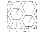
なおトレンチ206の存在は、逆の見方をすれば、主表面TSを頂面とするメサ構造の存在に対応している。好ましくはこの頂面の形状は、六方晶の場合、図7に示すように六角形である。
In other words, the presence of the
次に半導体装置の詳細について説明する。耐圧保持層2は、単結晶基板80の一方の主表面上に形成されている。耐圧保持層2上にはp型ボディ層3が形成されている。p型ボディ層3上には、n型ソースコンタクト層4が形成されている。このn型ソースコンタクト層4に取囲まれるように、p型のコンタクト領域5が形成されている。n型ソースコンタクト層4、p型ボディ層3および耐圧保持層2を部分的に除去することにより、トレンチ206により囲まれたメサ構造が形成されている。
Next, details of the semiconductor device will be described. The breakdown
トレンチ206の側面S1〜S6および底面上にはゲート絶縁膜8が形成されている。このゲート絶縁膜8はn型ソースコンタクト層4の上部表面上にまで延在している。このゲート絶縁膜8上であって、トレンチ206の内部を充填するように(つまり隣接するメサ構造の間の空間を充填するように)ゲート電極9が形成されている。すなわちゲート電極9はトレンチゲート構造を構成している。ゲート電極9の上部表面は、ゲート絶縁膜8においてn型ソースコンタクト層4の上部表面上に位置する部分の上面とほぼ同じ高さになっている。
A
ゲート絶縁膜8のうちn型ソースコンタクト層4の上部表面上にまで延在する部分とゲート電極9とを覆うように層間絶縁膜10が形成されている。層間絶縁膜10とゲート絶縁膜8の一部とを除去することにより、n型ソースコンタクト層4の一部とp型のコンタクト領域5とを露出するように開口部11が形成されている。この開口部11の内部を充填するとともに、p型のコンタクト領域5およびn型ソースコンタクト層4の一部と接触するようにソース電極12が形成されている。ソース電極12の上部表面と接触するとともに、層間絶縁膜10の上部表面上に延在するようにソース配線電極13が形成されている。また、単結晶基板80において耐圧保持層2が形成された主表面とは反対側の裏面上には、ドレイン電極14が形成されている。このドレイン電極14はオーミック電極である。
An interlayer insulating
次にMOSFET200の製造方法について説明する。
図8に示すように、単結晶基板80上に、主表面TSが設けられたエピタキシャル層209が形成される。具体的には、単結晶基板80の主表面MS上におけるエピタキシャル成長によって、導電型がn型であるエピタキシャル層209が形成される。このエピタキシャル成長は、たとえば原料ガスとしてシラン(SiH4)とプロパン(C3H8)との混合ガスを用い、キャリアガスとしてたとえば水素ガス(H2)を用いたCVD(Chemical Vapor Deposition)法により実施することができる。また、このときエピタキシャル層209にn型を付与するための不純物としてたとえば窒素(N)やリン(P)を導入することが好ましい。不純物の濃度は、たとえば5×1015cm-3以上5×1016cm-3以下とすることができる。
Next, a method for manufacturing
As shown in FIG. 8,
図9に示すように、エピタキシャル層209から、耐圧保持層2、p型ボディ層3およびn型ソースコンタクト層4が形成される。具体的には、エピタキシャル層209の上部表面層にイオン注入を行なうことにより、p型ボディ層3およびn型ソースコンタクト層4が形成され、イオン注入がなされなかった部分が耐圧保持層2となる。p型ボディ層3を形成するためのイオン注入においては、たとえばアルミニウム(Al)などのp型を付与するための不純物イオンが注入される。このとき、注入するイオンの加速エネルギーを調整することによりp型ボディ層3が形成される領域の深さを調整することができる。またn型を付与するための不純物イオンを、p型ボディ層3が形成された耐圧保持層2へイオン注入することにより、n型ソースコンタクト層4が形成される。n型を付与するための不純物としては、たとえばリン(P)などを用いることができる。
As shown in FIG. 9, breakdown
図10および図11に示すように、エピタキシャル層209の主表面TSの一部を覆うマスク17が形成される。マスク17として、たとえばシリコン酸化膜などの絶縁膜を用いることができる。マスク17の形成方法としては、たとえば以下のような工程を用いることができる。すなわち、n型ソースコンタクト層4の上部表面上に、CVD法などを用いてシリコン酸化膜を形成する。そして、このシリコン酸化膜上にフォトリソグラフィ法を用いて所定の開口パターンを有するレジスト膜(図示せず)を形成する。このレジスト膜をマスクとして用いて、シリコン酸化膜をエッチングにより除去する。その後レジスト膜を除去する。この結果、開口パターンを有するマスク17が形成される。
As shown in FIGS. 10 and 11, a
図12に示すように、単結晶基板80の主表面TSに対してほぼ垂直な側面を有する凹部16が形成される。具体的には、マスク17を用いて、n型ソースコンタクト層4、p型ボディ層3および耐圧保持層2の一部がエッチングされる。エッチングとしてはたとえば反応性イオンエッチング(RIE)またはイオンミリングを用いることができる。RIEとしては特に誘導結合プラズマ(ICP)RIEを用いることができる。具体的には、たとえば反応ガスとしてSF6またはSF6とO2との混合ガスを用いたICP−RIEを用いることができる。
As shown in FIG. 12,
図13および図14に示すように、主表面TSに対して傾斜した側面S1〜S6がエピタキシャル層209に設けられるように、トレンチ206が形成される。具体的には、マスク17が形成されたエピタキシャル層209の主表面TSに対して、熱エッチングが行われる。ここで熱エッチングとは、加熱されたエッチング対象へ反応性ガスを含むプロセスガス供給することによって生じる化学反応を用いて行われるエッチングである。本実施の形態においては、反応性ガスとして塩素系ガスが用いられ、好ましくは塩素ガスが用いられる。また熱エッチングは、好ましくは、塩素系ガスの分圧が50%以下である雰囲気下で行われる。また熱エッチングは、好ましくは、減圧雰囲気下で行われ、より好ましくは、減圧雰囲気は大気圧の1/10以下の圧力を有する。また熱エッチングは、好ましくは、エピタキシャル層209が設けられた単結晶基板80の温度(熱処理温度)を1000℃以上とする条件で行われる。
As shown in FIGS. 13 and 14,
次に熱エッチングの詳細の一例について、以下に説明する。
プロセスガスとしては、酸素ガスと塩素ガスとの混合ガスを反応ガスとして用い、熱処理温度をたとえば700℃以上1200℃以下としたエッチングを行なう。熱処理温度は、好ましくは700℃以上1200℃以下である。1200℃以下の場合、熱処理のための装置に石英部材を用いることができる。温度の上限は、より好ましくは1100℃、さらに好ましくは1000℃である。温度の下限は、より好ましくは800℃、さらに好ましくは900℃である。この場合、エッチング速度を十分実用的な値とすることができる。
Next, an example of details of thermal etching will be described below.
As a process gas, a mixed gas of oxygen gas and chlorine gas is used as a reaction gas, and etching is performed at a heat treatment temperature of, for example, 700 ° C. or higher and 1200 ° C. or lower. The heat treatment temperature is preferably 700 ° C. or higher and 1200 ° C. or lower. In the case of 1200 ° C. or lower, a quartz member can be used in an apparatus for heat treatment. The upper limit of the temperature is more preferably 1100 ° C, still more preferably 1000 ° C. The lower limit of the temperature is more preferably 800 ° C, and still more preferably 900 ° C. In this case, the etching rate can be set to a sufficiently practical value.
ここで、上記熱エッチング工程の条件については、SiC+mO2+nCl2→SiClx+COy(ただし、m、n、x、yは正の数)と表される反応式において、0.5≦x≦2.0、1.0≦y≦2.0というxおよびyの条件が満たされる場合に主な反応が進み、x=4、y=2という条件の場合が最も反応(熱エッチング)が進む。ただし上記mおよびnは、実際に反応している酸素ガスおよび塩素ガスの量を表しており、プロセスガスとして供給される量とは異なる。この熱エッチングにおいて供給される塩素の流量に対する酸素の流量の比率は0.1以上2.0以下となることが好ましく、より好ましくはこの比率の下限は0.25である。 Here, with respect to the conditions of the thermal etching step, 0.5 ≦ x ≦ in the reaction formula represented by SiC + mO 2 + nCl 2 → SiCl x + CO y (where m, n, x, and y are positive numbers). The main reaction proceeds when the x and y conditions of 2.0 and 1.0 ≦ y ≦ 2.0 are satisfied, and the reaction (thermal etching) proceeds most when the conditions of x = 4 and y = 2. . However, the above m and n represent the amounts of oxygen gas and chlorine gas which are actually reacted, and are different from the amounts supplied as process gases. The ratio of the flow rate of oxygen to the flow rate of chlorine supplied in this thermal etching is preferably 0.1 or more and 2.0 or less, and more preferably the lower limit of this ratio is 0.25.
なお、反応ガスは、上述した塩素ガスと酸素ガスとに加えて、キャリアガスを含んでいてもよい。キャリアガスとしては、たとえば窒素(N2)ガス、アルゴンガス、ヘリウムガスなどを用いることができる。そして、上述のように熱処理温度を700℃以上1000℃以下とした場合、SiCのエッチング速度はたとえば70μm/hr程度になる。また、この場合にマスク17として酸化珪素(SiO2)を用いると、SiO2に対するSiCの選択比を極めて大きくすることができるので、SiCのエッチング中にSiO2からなるマスク17は実質的にエッチングされない。
Note that the reaction gas may contain a carrier gas in addition to the above-described chlorine gas and oxygen gas. As the carrier gas, for example, nitrogen (N 2 ) gas, argon gas, helium gas or the like can be used. When the heat treatment temperature is set to 700 ° C. or more and 1000 ° C. or less as described above, the etching rate of SiC is, for example, about 70 μm / hr. In this case, if silicon oxide (SiO 2 ) is used as the
次にマスク17がエッチングなど任意の方法により除去される。
図15および図16に示すように、コンタクト領域5が形成される。なお図16から分かるように、トレンチ206の平面形状は、単位胞(1つのメサ構造を取り囲む環状のトレンチ206)の平面形状が六角形状である網目形状となっている。また、p型のコンタクト領域5は、図16に示すようにメサ構造の上部表面におけるほぼ中央部に配置されている。また、p型のコンタクト領域5の平面形状は、メサ構造の上部表面の外周形状と同じであって、六角形状となっている。次に、上述したイオン注入により注入された不純物を活性化するための活性化アニール工程を実施する。この活性化アニール工程においては、炭化珪素からなるエピタキシャル層の表面上(たとえばメサ構造の側壁上)に特にキャップ層を形成することなくアニール処理を実施する。なお、上述したキャップ層を形成したうえで活性化アニール工程を実施してもよい。また、たとえばn型ソースコンタクト層4およびp型のコンタクト領域5の上部表面上のみにキャップ層を設けた構成として、活性化アニール処理を実施してもよい。
Next, the
As shown in FIGS. 15 and 16,
図17に示すように、エピタキシャル層209の側面S1〜S6上にゲート絶縁膜8が形成される。具体的には、トレンチ206の内部からn型ソースコンタクト層4およびp型のコンタクト領域5の上部表面上にまで延在するようにゲート絶縁膜8が形成される。ゲート絶縁膜8としては、たとえばエピタキシャル層209を熱酸化することにより得られる酸化膜(酸化珪素膜)を用いることができる。
As shown in FIG. 17,
図18に示すように、ゲート絶縁膜8を介してエピタキシャル層209の側面S1〜S6の各々に対向するゲート電極9が形成される。具体的には、トレンチ206の内部を充填するように、ゲート絶縁膜8上にゲート電極9が形成される。ゲート電極9の形成方法としては、たとえば以下のような方法を用いることができる。まず、ゲート絶縁膜8上において、トレンチ206の内部およびp型のコンタクト領域5上の領域にまで延在するゲート電極となるべき導電体膜が、スパッタリング法などを用いて形成される。導電体膜の材料としては導電性を有する材料であれば金属など任意の材料を用いることができる。その後、エッチバックあるいはCMP(Chemical Mechanical Polishing)法など任意の方法を用いて、トレンチ206の内部以外の領域に形成された導電体膜の部分が除去される。この結果、トレンチ206の内部を充填するような導電体膜が残存し、当該導電体膜によりゲート電極9が構成される。
As shown in FIG. 18,
図19を参照して、ゲート電極9の上部表面、およびp型のコンタクト領域5上において露出しているゲート絶縁膜8の上部表面上を覆うように層間絶縁膜10が形成される。層間絶縁膜10としては、絶縁性を有する材料であれば任意の材料を用いることができる。そして、層間絶縁膜10上に、パターンを有するレジスト膜(図示せず)が、フォトリソグラフィ法を用いて形成される。当該レジスト膜にはp型のコンタクト領域5上に位置する領域に開口パターンが形成される。そして、このレジスト膜をマスクとして用いて、エッチングにより層間絶縁膜10およびゲート絶縁膜8が部分的にエッチングにより除去される。この結果、層間絶縁膜10およびゲート絶縁膜8には開口部11(図19参照)が形成される。この開口部11の底部においては、p型のコンタクト領域5およびn型ソースコンタクト層4の一部が露出した状態となる。
Referring to FIG. 19,
その後、開口部11の内部を充填するとともに、上述したレジスト膜の上部表面上を覆うように導電体膜が形成される。その後、薬液などを用いてレジスト膜を除去することにより、レジスト膜上に形成されていた導電体膜の部分も同時に除去する(リストオフ)。この結果、開口部11の内部に充填された導電体膜によりソース電極12を形成できる。このソース電極12はp型のコンタクト領域5およびn型ソースコンタクト層4とオーミック接触したオーミック電極である。
Thereafter, a conductor film is formed so as to fill the inside of the
また、単結晶基板80の裏面側(耐圧保持層2が形成された主表面と反対側の表面側)に、ドレイン電極14が形成される。ドレイン電極14としては、単結晶基板80とオーミック接触が可能な材料であれば任意の材料を用いることができる。
Further,
再び図6を参照して、ソース電極12の上部表面に接触するとともに、層間絶縁膜10の上部表面上に延在するソース配線電極13がスパッタリング法などの任意の方法を用いて形成される。以上によりMOSFET200が得られる。
Referring to FIG. 6 again,
本実施の形態によれば、大きなチャネル移動度を有する6つの異なる面を設けることができる。この6つの面を利用することで、六角形の形状を平面パターンとして有する(図7参照)MOSFET200において、チャネル移動度を高くすることができる。
According to the present embodiment, it is possible to provide six different surfaces having a large channel mobility. By using these six surfaces, channel mobility can be increased in
なおMOSFET200のトレンチ206は平坦な底面を有するが、MOSFET200vのトレンチ206V(図20)のように、V字状のトレンチが設けられてもよい。この場合、MOSFETをより集積化することが可能である。
Although the
(実施の形態3)
図21に示すように、本実施の形態の炭化珪素半導体装置は、MOSFET300であり、実施の形態2のMOSFET200と同様に、縦型のトレンチゲート型MOSFETである。ただしMOSFET300のエピタキシャル層309は、MOSFE200のエピタキシャル層209(図7)と異なり、図22に示すように、平面視においてストライプ状の形状を有するトレンチ306を有する。トレンチ306は、エピタキシャル層309の表面としての側面T1およびT2(第1および第2の領域)を有する。トレンチ306は、開口に向かって広がるようなテーパ形状を有し、よって主表面TSに対して側面T1およびT2は傾いている。側面T1およびT2のうちp型ボディ層3によって形成されている部分は、MOSFET300のチャネル面を構成している。
(Embodiment 3)
As shown in FIG. 21, the silicon carbide semiconductor device of the present embodiment is
側面T1およびT2のそれぞれは、p型ボディ層3上において第1および第2の面方位を少なくとも部分的に有する。第1および第2の面方位は互いに異なる。また第1および第2の面方位は、実質的に、(0−33−8)面、(30−3−8)面、(−330−8)面、(03−3−8)面、(−303−8)面および(3−30−8)面のいずれかである。言い換えると、第1および第2の面方位の{0001}面に対するオフ方位は<1−100>方向に対して±5°の範囲内にある。そして第1および第2の面方位の<1−100>方向における{03−38}面に対するオフ角は−3°以上3°以下である。そして第1〜第6の面方位の(000−1)面に対する傾きは90°未満である。たとえば、第1の面が実質的に(0−33−8)面であり、第2の面が実質的に(03−3−8)面である。
Each of side surfaces T <b> 1 and T <b> 2 has at least a part of first and second plane orientations on p-
本実施の形態によれば、大きなチャネル移動度を有する2つの異なる面を設けることができる。この2つの面を利用することで、ストライプ状の形状を平面パターンとして有する(図22参照)MOSFET300において、チャネル移動度を高くすることができる。
According to the present embodiment, it is possible to provide two different surfaces having a large channel mobility. By using these two surfaces, channel mobility can be increased in
(界面準位密度の評価)
MOSキャパシタ(図23)を用いた界面準位密度の測定結果の例について説明する。
(Evaluation of interface state density)
An example of the measurement result of the interface state density using the MOS capacitor (FIG. 23) will be described.
実施例として、(0−33−8)面の面方位を有する上面を有する炭化珪素基板を用いてMOSキャパシタを作製した。比較例1として(03−38)面の面方位を有する上面を有する炭化珪素基板を用いてMOSキャパシタを作製した。また比較例2として(0001)面の面方位を有する上面を有する炭化珪素基板を用いてMOSキャパシタを作製した。 As an example, a MOS capacitor was fabricated using a silicon carbide substrate having an upper surface having a (0-33-8) plane orientation. As Comparative Example 1, a MOS capacitor was manufactured using a silicon carbide substrate having an upper surface having a (03-38) plane orientation. As Comparative Example 2, a MOS capacitor was fabricated using a silicon carbide substrate having an upper surface having a (0001) plane orientation.
MOSキャパシタの製造方法は次のとおりである。まずn型の炭化珪素基板402を準備した。炭化珪素基板402の上面におけるエピタキシャル成長によって上面上にn型SiC層403を形成した。n型SiC層403上にゲート酸化膜404(SiO2)を形成した。次にアニールを行った。具体的には、NO雰囲気中での第1アニールと、Ar雰囲気中での第2アニールとを行った。両アニールの各々において、アニール温度は1250℃とされ、アニール時間は1時間とされた。次にゲート酸化膜の上にAl蒸着によってゲート電極405を形成した。ゲート電極405の大きさは、300〜500μmφとした。また炭化珪素基板402の裏面上にコンタクト電極401(Body)を形成した。具体的には、Ni蒸着と、Ar雰囲気中、1000℃、2分間のRTAとを行った。
The manufacturing method of the MOS capacitor is as follows. First, an n-type
伝導電子帯のエネルギーECを基準としたエネルギーE−ECと、界面準位密度との関係を測定した(図24)。グラフ中、実線P1は(03−38)面に対応し、破線P2は(0001)面に対応し、実線P3は(0−33−8)面に対応している。(0−33−8)面の場合(実線P3)は、エネルギーE−ECの値に関わらず界面準位密度が5×1011cm-2eV-1未満であった。また(0−33−8)面の場合は、エネルギーE−EC(eV)が0以上0.5以下の範囲内において、界面準位密度はおおよそ一定であり、その変動は1桁内に十分に収まっていた。また(0−33−8)面の場合の方が(03−38)面に比して界面準位密度が低く、特に伝導電子帯から浅いエネルギー値においてその差異が顕著であった。すなわち(0−33−8)面上での界面準位密度は(03−38)面または(0001)面上での界面準位密度に比して小さかった。このことから、(0−33−8)面上に、より良好な界面が形成されていると推測される。 The relationship between the energy E-E C based on the energy E C of the conduction electron band and the interface state density was measured (FIG. 24). In the graph, the solid line P1 corresponds to the (03-38) plane, the broken line P2 corresponds to the (0001) plane, and the solid line P3 corresponds to the (0-33-8) plane. In the case of the (0-33-8) plane (solid line P3), the interface state density was less than 5 × 10 11 cm −2 eV −1 regardless of the value of energy E-E C. In the case of the (0-33-8) plane, the interface state density is approximately constant within the range where the energy E-E C (eV) is 0 or more and 0.5 or less, and the fluctuation is within one digit. It was enough. In the case of the (0-33-8) plane, the interface state density was lower than that of the (03-38) plane, and the difference was particularly remarkable at an energy value shallow from the conduction electron band. That is, the interface state density on the (0-33-8) plane was smaller than the interface state density on the (03-38) plane or the (0001) plane. From this, it is presumed that a better interface is formed on the (0-33-8) plane.
なお(30−3−8)面、(−330−8)面、(03−3−8)面、(−303−8)面および(3−30−8)面の各々は、上述した物性の観点で(0−33−8)面と等価である。 Each of the (30-3-8) plane, the (-330-8) plane, the (03-3-8) plane, the (-303-8) plane, and the (3-30-8) plane has the above-mentioned physical properties. Is equivalent to the (0-33-8) plane.
(不純物濃度が低い場合のチャネル移動度の評価)
横型MOSFET(図25)を用いたチャネル移動度の測定結果の例について説明する。
(Evaluation of channel mobility when impurity concentration is low)
An example of measurement results of channel mobility using a lateral MOSFET (FIG. 25) will be described.
実施例として、(0−33−8)面の面方位を有する上面を有する炭化珪素基板を用いてMOSFETを作製した。具体的には、[11−20]方向に平行な方向にソース/ドレインが配列されるもの(実施例1)と、[11−20]方向に垂直な方向にソース/ドレインが配列されるもの(実施例2)とを作製した。また比較例として(03−38)面の面方位を有する上面を有する炭化珪素基板を用いてMOSFETを作製した。具体的には、[11−20]方向に平行な方向にソース/ドレインが配列されるもの(比較例1)と、[11−20]方向に垂直な方向にソース/ドレインが配列されるもの(比較例2)とを作製した。 As an example, a MOSFET was manufactured using a silicon carbide substrate having an upper surface having a (0-33-8) plane orientation. Specifically, the source / drain is arranged in a direction parallel to the [11-20] direction (Example 1), and the source / drain is arranged in a direction perpendicular to the [11-20] direction. Example 2 was prepared. As a comparative example, a MOSFET was fabricated using a silicon carbide substrate having an upper surface having a (03-38) plane orientation. Specifically, the source / drain is arranged in a direction parallel to the [11-20] direction (Comparative Example 1), and the source / drain is arranged in a direction perpendicular to the [11-20] direction. (Comparative Example 2) was prepared.
MOSFETの製造方法は次のとおりである。n型SiC基板501の上面上におけるエピタキシャル成長によってn型SiC層502を形成した。n型SiC層502上にAlイオンの注入によりpウエル層503を形成した。pウエル層503の不純物濃度は2×1016cm-3程度、深さは700nm程度とされた。pウエル層503中にリソグラフィ技術を用いて、n+ソース領域504と、n+ドレイン領域505と、p+ボディ領域506とを形成した。p型はAlイオンを用いて、n型はPイオンを用いて付与された。次にキャップが形成された。次にAr雰囲気中、1700℃、20分間の活性化アニールを行った。その後、犠牲酸化によりエピタキシャル表面を清浄化した。次にゲート酸化膜507(SiO2)を形成した。次にゲート酸化膜507のアニールを行った。具体的には、NO雰囲気中での第1アニールと、Ar雰囲気中での第2アニールとを行った。両アニールの各々において、アニール温度は1250℃とされ、アニール時間は1時間とされた。次にn+ソース領域504と、n+ドレイン領域505と、p+ボディ領域506との各々の上に、Ni蒸着と、Ar雰囲気中、1000℃、2分間のRTAとを行った。さらに各々の上にAl蒸着を行なった。これによりソース電極509と、ドレイン電極510と、ボディ電極511とを形成した。またゲート酸化膜507の上にAl蒸着によってゲート電極508を形成した。
The method for manufacturing the MOSFET is as follows. N-
主な測定結果を以下の表に示す。 The main measurement results are shown in the following table.

なおdoxはゲート酸化膜507の厚さである。またVthはしきい値電圧である。またμfe-maxはチャネル移動度の最大値である。S値については後述する。
D ox is the thickness of the
この結果から、実施例1および実施例2の各々のμfe-maxは、比較例1および2の各々よりも大きかった。実施例1および2の間の相違すなわちチャネル方向の相違は、μfe-maxに大きな影響を及ぼさなかった。(0−33−8)面の方が高いμfe-maxを有する理由は、前述したように、(0−33−8)面の方が(03−38)面に比して低い界面準位密度を有するためと推定される。 From this result, each of μfe-max in Example 1 and Example 2 was larger than that in each of Comparative Examples 1 and 2. The difference between Examples 1 and 2, ie the difference in channel direction, did not have a significant effect on μ fe-max . The reason why the (0-33-8) plane has a higher μ fe-max is that, as described above, the (0-33-8) plane has a lower interface state than the (03-38) plane. This is presumed to have a density of units.
図26および図27のそれぞれのグラフは実施例1および2におけるゲート電圧VGに対するドレイン電流IDを示している。左側の縦軸はログスケールによる。右側の縦軸はリニアスケールによるものであり、かつ係数L/COXWが付されている。Lはチャネル長であり、100μmとされた。Wはチャネル幅であり200μmとされた。COXはゲート酸化膜507の容量である。
Each graph of FIGS. 26 and 27 show the drain current I D with respect to the gate voltage V G of Example 1 and 2. The left vertical axis depends on the log scale. The vertical axis on the right is based on a linear scale, and a coefficient L / C OX W is attached. L is the channel length and was set to 100 μm. W is the channel width and was 200 μm. C OX is the capacitance of the
なお(30−3−8)面、(−330−8)面、(03−3−8)面、(−303−8)面および(3−30−8)面の各々は、上述した物性の観点で(0−33−8)面と等価である。また上述した実施例1および2においてはpウエル層503の不純物濃度は2×1016cm-3程度とされたが、この不純物濃度が1×1016cm-3まで低減されても、ゲート電圧VGのしきい値を2.5V以上とすることができた。
Each of the (30-3-8) plane, the (-330-8) plane, the (03-3-8) plane, the (-303-8) plane, and the (3-30-8) plane has the above-mentioned physical properties. Is equivalent to the (0-33-8) plane. In Examples 1 and 2 described above, the impurity concentration of the p-
(不純物濃度が高い場合のチャネル移動度の評価)
上記実施例1および2においてはpウエル層503の不純物濃度、すなわちチャネルの不純物濃度が2×1016cm-3程度とされた。実施例3においては、不純物濃度が1×1017cm-3とされた。他の条件は上記の実施例とほぼ同様である。ドレイン電圧VDを0.1Vとした場合における、実施例3のチャネル移動度μfeの測定結果(図28)から、その最大値であるチャネル移動度μfe-maxは70cm2/Vs以上であった。またしきい値電圧Vthは4.5Vであった。
(Evaluation of channel mobility when impurity concentration is high)
In Examples 1 and 2, the impurity concentration of the p-
なお本明細書に記載のしきい値電圧Vthは、図29に示すように、IDL/COXWの直線状の増加領域LPに対して1次関数による近似を行い、この関数とVG軸との交点を利用して求めた。このVthの算出方法の詳細について、以下に説明する。 As shown in FIG. 29, the threshold voltage V th described in this specification is approximated by a linear function with respect to the linear increase region LP of I D L / C OX W. It calculated | required using the intersection with VG axis. Details of the V th calculation method will be described below.
ドレイン電流IDは、チャネル移動度をμ、ドレイン電圧をVDとすると、以下の式(1)で表される。 The drain current I D is expressed by the following equation (1), where the channel mobility is μ and the drain voltage is V D.
式(1)を変形すると、下記の式(2)が得られる。 When formula (1) is modified, the following formula (2) is obtained.
式(2)は、VGを変数とする1次関数であり、この関数で表される部分が、直線状の増加領域LP(図29)に対応している。よって直線状の増加領域LPを外挿した場合のゲート電圧VG軸との交点におけるVGの値をXとすると、VG=Xにおいて式(2)の括弧内はゼロとなる。すなわち、X=VD/2+Vthである。よってVth=X−VD/2により、しきい値電圧Vthを求めることができる。 Equation (2) is a linear function with V G as a variable, and the portion represented by this function corresponds to the linear increase region LP (FIG. 29). Therefore, when the value of V G at the intersection with the gate voltage V G axis when the linear increase region LP is extrapolated is X, the value in parentheses in Equation (2) is zero when V G = X. That is, X = V D / 2 + V th . Therefore, the threshold voltage V th can be obtained from V th = X−V D / 2.
(S値の評価)
S値は、サブスレッショルド係数とも称される。上記の表1を参照して、実施例1および2のS値は、比較例1および2のS値に比して顕著に低く、共に200mV/decade以下であった。このことから、実施例1および2に対応する(0−33−8)面をチャネルに用いることで、急峻なスイッチング特性を有する炭化珪素半導体装置が得られることがわかる。
(Evaluation of S value)
The S value is also referred to as a subthreshold coefficient. Referring to Table 1 above, the S values of Examples 1 and 2 were significantly lower than those of Comparative Examples 1 and 2, and both were 200 mV / decade or less. This shows that a silicon carbide semiconductor device having steep switching characteristics can be obtained by using the (0-33-8) plane corresponding to Examples 1 and 2 as a channel.
(30−3−8)面、(−330−8)面、(03−3−8)面、(−303−8)面および(3−30−8)面の各々は、上述した物性の観点で(0−33−8)面と等価である。 Each of the (30-3-8) plane, the (-330-8) plane, the (03-3-8) plane, the (-303-8) plane, and the (3-30-8) plane has the physical properties described above. From the viewpoint, it is equivalent to the (0-33-8) plane.
なおS値の定義は以下のとおりである。 The definition of the S value is as follows.
式(3)における微分は、ゲート電圧VGの増加にともなってlog10IDが線形に増大する領域(図30におけるサブスレッシュドスロープSS)でのものである。たとえば、Vth≦VG≦Vth+0.3(V)の範囲での0.1Vステップでのデータから平均的に算出され得る。 Derivative of the formula (3) are those in (sub threshold de slope SS in FIG. 30) regions log 10 I D increases linearly with an increase of the gate voltage V G. For example, it can be averagely calculated from data at 0.1 V step in the range of V th ≦ V G ≦ V th +0.3 (V).
(炭化珪素層の表面が複合面から形成される場合について)
炭化珪素層(たとえば図6のエピタキシャル層209)の表面が有する領域(たとえば、第1の領域としての図6の側面S1)は、特定の面方位を部分的に有する複合面CP(図31)であってもよい。ここで、特定の面方位とは、(0−33−8)面、(30−3−8)面、(−330−8)面、(03−3−8)面、(−303−8)面および(3−30−8)面のいずれかである。また複合面CPとは、微視的に見た場合に、第1の面からなる第1の部分P1と、第1の面と異なる面からなる第2の部分P2とを含む面である。ここで「微視的」とは、原子間隔程度の寸法を考慮することを意味する。たとえば、第1および第2の部分P1、P2の各々は、第1および第2の部分P1、P2が互いに隣り合う方向(周期方向)において、原子間隔の2倍程度の幅寸法を有し、周期方向と交差する方向において、原子間隔に比して十分に大きな寸法を有するものであってもよい。
(When the surface of the silicon carbide layer is formed from a composite surface)
A region (for example, side surface S1 in FIG. 6 as the first region) included in the surface of the silicon carbide layer (for example,
今回開示された実施の形態および実施例はすべての点で例示であって制限的なものではないと考えられるべきである。本発明の特許請求の範囲は上記した説明ではなくて請求の範囲によって示され、特許請求の範囲と均等の意味および範囲内でのすべての変更が含まれることが意図される。 It should be understood that the embodiments and examples disclosed herein are illustrative and non-restrictive in every respect. The scope of the claims of the present invention is defined by the terms of the claims, rather than the description above, and is intended to include any modifications within the scope and meaning equivalent to the terms of the claims.
8,126 ゲート絶縁膜(絶縁膜)、9,110,405,508 ゲート電極、80 単結晶基板、100,200,200v,300 MOSFET(炭化珪素半導体装置、109,209,309 エピタキシャル層(炭化珪素層)、206,206V,306 トレンチ、R1 第1の領域、S1〜S6 側面(第1〜第6の領域)、T1およびT2 側面(第1および第2の領域)。 8,126 Gate insulating film (insulating film) 9,110,405,508 Gate electrode, 80 Single crystal substrate, 100,200,200v, 300 MOSFET (silicon carbide semiconductor device, 109,209,309 epitaxial layer (silicon carbide) Layer), 206, 206V, 306 trench, R1 first region, S1-S6 side surfaces (first to sixth regions), T1 and T2 side surfaces (first and second regions).
Claims (9)
前記絶縁膜に覆われた側面を有するトレンチを含む炭化珪素層とを備え、前記側面は第1の領域を含み、前記第1の領域は第1の面方位を少なくとも部分的に有し、前記第1の面方位は、(0−33−8)面、(30−3−8)面、(−330−8)面、(03−3−8)面、(−303−8)面および(3−30−8)面のいずれかであり、
前記トレンチの前記側面は第2の領域をさらに有し、前記第2の領域は前記第1の面方位と異なる第2の面方位を少なくとも部分的に有し、前記第2の面方位は、(0−33−8)面、(30−3−8)面、(−330−8)面、(03−3−8)面、(−303−8)面および(3−30−8)面のいずれかであり、
前記トレンチの前記側面は第3〜第6の領域をさらに有し、前記第3〜第6の領域のそれぞれは第3〜第6の面方位を少なくとも部分的に有し、前記第1〜第6の面方位は互いに異なり、前記第1〜第6の面方位の各々は(0−33−8)面、(30−3−8)面、(−330−8)面、(03−3−8)面、(−303−8)面および(3−30−8)面のいずれかである、炭化珪素半導体装置。 An insulating film;
A silicon carbide layer including a trench having a side surface covered with the insulating film, the side surface including a first region, and the first region at least partially has a first surface orientation, The first plane orientation is (0-33-8) plane, (30-3-8) plane, (-330-8) plane, (03-3-8) plane, (-303-8) plane and Any of (3-30-8) planes,
The side surface of the trench further includes a second region, and the second region has at least partially a second plane orientation different from the first plane orientation, and the second plane orientation is (0-33-8) plane, (30-3-8) plane, (-330-8) plane, (03-3-8) plane, (-303-8) plane and (3-30-8) Ri der either side,
The side surface of the trench further includes third to sixth regions, and each of the third to sixth regions has at least partly a third to sixth surface orientation, 6 have different plane orientations, and the first to sixth plane orientations are (0-33-8) plane, (30-3-8) plane, (-330-8) plane, (03-3). -8) plane, (- 303-8) plane and (3-30-8) Ru der either surface, the silicon carbide semiconductor device.
前記絶縁膜に覆われた側面を有するトレンチを含む炭化珪素層とを備え、前記側面は第1の領域を含み、前記第1の領域は第1の面方位を少なくとも部分的に有し、前記第1の面方位の{0001}面に対するオフ方位は<1−100>方向に対して±5°の範囲内にあり、前記第1の面方位の<1−100>方向における{03−38}面に対するオフ角は−3°以上3°以下であり、前記第1の面方位の(000−1)面に対する傾きは90°未満であり、
前記トレンチの前記側面は第2の領域をさらに有し、前記第2の領域は前記第1の面方位と異なる第2の面方位を少なくとも部分的に有し、前記第2の面方位の{0001}面に対するオフ方位は<1−100>方向に対して±5°の範囲内にあり、前記第2の面方位の<1−100>方向における{03−38}面に対するオフ角は−3°以上3°以下であり、前記第2の面方位の(000−1)面に対する傾きは90°未満であり、
前記トレンチの前記側面は第3〜第6の領域をさらに有し、前記第3〜第6の領域のそれぞれは第3〜第6の面方位を少なくとも部分的に有し、前記第1〜第6の面方位は互いに異なり、前記第1〜第6の面方位の各々の{0001}面に対するオフ方位は<1−100>方向に対して±5°の範囲内にあり、前記第1〜第6の面方位の各々の<1−100>方向における{03−38}面に対するオフ角は−3°以上3°以下であり、前記第1〜第6の面方位の各々の(000−1)面に対する傾きは90°未満である、炭化珪素半導体装置。 An insulating film;
A silicon carbide layer including a trench having a side surface covered with the insulating film, the side surface including a first region, and the first region at least partially has a first surface orientation, The off orientation with respect to the {0001} plane of the first plane orientation is in the range of ± 5 ° with respect to the <1-100> direction, and {03-38 in the <1-100> direction of the first plane orientation. } The off angle with respect to the plane is -3 ° or more and 3 ° or less, and the inclination of the first plane orientation with respect to the (000-1) plane is less than 90 °,
The side surface of the trench further includes a second region, and the second region has at least partially a second surface orientation different from the first surface orientation, and the second surface orientation { The off orientation with respect to the 0001} plane is within ± 5 ° with respect to the <1-100> direction, and the off angle with respect to the {03-38} plane in the <1-100> direction of the second plane orientation is − 3 ° and not more than 3 ° or less, the inclination with respect to the (000-1) plane of the second surface orientation is Ri der less than 90 °,
The side surface of the trench further includes third to sixth regions, and each of the third to sixth regions has at least partly a third to sixth surface orientation, 6 are different from each other, and the off-orientation of each of the first to sixth plane orientations with respect to the {0001} plane is within a range of ± 5 ° with respect to the <1-100> direction. The off angle with respect to the {03-38} plane in the <1-100> direction of each of the sixth plane orientations is −3 ° or more and 3 ° or less, and each of the first to sixth plane orientations is (000− 1) slope Ru der less than 90 ° with respect to surface, the silicon carbide semiconductor device.
Priority Applications (4)
| Application Number | Priority Date | Filing Date | Title |
|---|---|---|---|
| PCT/JP2012/082493 WO2013114743A1 (en) | 2012-02-01 | 2012-12-14 | Silicon carbide semiconductor device |
| CN201280065718.8A CN104025300B (en) | 2012-02-01 | 2012-12-14 | Silicon carbide semiconductor device |
| EP12867527.9A EP2811529B1 (en) | 2012-02-01 | 2012-12-14 | Silicon carbide semiconductor device |
| US13/722,486 US8829535B2 (en) | 2012-02-01 | 2012-12-20 | Silicon carbide semiconductor device |
Applications Claiming Priority (2)
| Application Number | Priority Date | Filing Date | Title |
|---|---|---|---|
| US201261593681P | 2012-02-01 | 2012-02-01 | |
| US61/593681 | 2012-02-01 |
Publications (2)
| Publication Number | Publication Date |
|---|---|
| JP2013162118A JP2013162118A (en) | 2013-08-19 |
| JP6119100B2 true JP6119100B2 (en) | 2017-04-26 |
Family
ID=49174085
Family Applications (1)
| Application Number | Title | Priority Date | Filing Date |
|---|---|---|---|
| JP2012036988A Active JP6119100B2 (en) | 2012-02-01 | 2012-02-23 | Silicon carbide semiconductor device |
Country Status (5)
| Country | Link |
|---|---|
| US (1) | US8829535B2 (en) |
| EP (1) | EP2811529B1 (en) |
| JP (1) | JP6119100B2 (en) |
| CN (1) | CN104025300B (en) |
| WO (1) | WO2013114743A1 (en) |
Cited By (1)
| Publication number | Priority date | Publication date | Assignee | Title |
|---|---|---|---|---|
| US12046642B2 (en) | 2021-01-21 | 2024-07-23 | Fuji Electric Co., Ltd. | Silicon carbide semiconductor device and method of manufacturing silicon carbide semiconductor device |
Families Citing this family (6)
| Publication number | Priority date | Publication date | Assignee | Title |
|---|---|---|---|---|
| JP5954140B2 (en) * | 2012-11-29 | 2016-07-20 | 住友電気工業株式会社 | Silicon carbide semiconductor device |
| JP6183080B2 (en) * | 2013-09-09 | 2017-08-23 | 住友電気工業株式会社 | Silicon carbide semiconductor device and manufacturing method thereof |
| JP2015056544A (en) * | 2013-09-12 | 2015-03-23 | 住友電気工業株式会社 | Silicon carbide semiconductor device and method for manufacturing the same |
| JP6294208B2 (en) * | 2014-10-17 | 2018-03-14 | トヨタ自動車株式会社 | Method for manufacturing insulated gate switching element having trench gate electrode |
| JP7166053B2 (en) | 2017-12-21 | 2022-11-07 | 株式会社東芝 | Semiconductor devices, inverter circuits, drive devices, vehicles, and elevators |
| CN111403280A (en) * | 2020-03-31 | 2020-07-10 | 中国科学院微电子研究所 | Silicon carbide MOS capacitor device and manufacturing method thereof |
Family Cites Families (16)
| Publication number | Priority date | Publication date | Assignee | Title |
|---|---|---|---|---|
| JP3610721B2 (en) * | 1997-03-05 | 2005-01-19 | 株式会社デンソー | Silicon carbide semiconductor device |
| US6057558A (en) * | 1997-03-05 | 2000-05-02 | Denson Corporation | Silicon carbide semiconductor device and manufacturing method thereof |
| JP4843854B2 (en) | 2001-03-05 | 2011-12-21 | 住友電気工業株式会社 | MOS device |
| JP4581270B2 (en) | 2001-03-05 | 2010-11-17 | 住友電気工業株式会社 | SiC semiconductor ion-implanted layer and method of manufacturing the same |
| JP5017768B2 (en) * | 2004-05-31 | 2012-09-05 | 富士電機株式会社 | Silicon carbide semiconductor element |
| JP5017855B2 (en) * | 2005-12-14 | 2012-09-05 | 富士電機株式会社 | Manufacturing method of semiconductor device |
| JP2010192697A (en) * | 2009-02-18 | 2010-09-02 | Sumitomo Electric Ind Ltd | Silicon carbide substrate and method of manufacturing silicon carbide substrate |
| JPWO2010110252A1 (en) * | 2009-03-27 | 2012-09-27 | 住友電気工業株式会社 | MOSFET and MOSFET manufacturing method |
| WO2010110253A1 (en) * | 2009-03-27 | 2010-09-30 | 住友電気工業株式会社 | Mosfet and method for manufacturing mosfet |
| TW201108388A (en) * | 2009-04-10 | 2011-03-01 | Sumitomo Electric Industries | Insulated gate field effect transistor |
| EP2432020A4 (en) * | 2009-05-11 | 2013-06-26 | Sumitomo Electric Industries | SEMICONDUCTOR DEVICE |
| JPWO2011052321A1 (en) * | 2009-10-30 | 2013-03-14 | 住友電気工業株式会社 | Method for manufacturing silicon carbide substrate and silicon carbide substrate |
| CN102725849B (en) * | 2010-01-27 | 2015-09-09 | 住友电气工业株式会社 | Sic semiconductor device and manufacture method thereof |
| US9947782B2 (en) * | 2010-03-23 | 2018-04-17 | Sumitomo Electric Industries, Ltd. | Semiconductor device and method for manufacturing same |
| JP2011233669A (en) * | 2010-04-27 | 2011-11-17 | Sumitomo Electric Ind Ltd | Semiconductor device |
| JP2012004494A (en) * | 2010-06-21 | 2012-01-05 | Sumitomo Electric Ind Ltd | Manufacturing method and manufacturing apparatus of silicon carbide substrate |
-
2012
- 2012-02-23 JP JP2012036988A patent/JP6119100B2/en active Active
- 2012-12-14 WO PCT/JP2012/082493 patent/WO2013114743A1/en active Application Filing
- 2012-12-14 EP EP12867527.9A patent/EP2811529B1/en active Active
- 2012-12-14 CN CN201280065718.8A patent/CN104025300B/en active Active
- 2012-12-20 US US13/722,486 patent/US8829535B2/en active Active
Cited By (1)
| Publication number | Priority date | Publication date | Assignee | Title |
|---|---|---|---|---|
| US12046642B2 (en) | 2021-01-21 | 2024-07-23 | Fuji Electric Co., Ltd. | Silicon carbide semiconductor device and method of manufacturing silicon carbide semiconductor device |
Also Published As
| Publication number | Publication date |
|---|---|
| WO2013114743A1 (en) | 2013-08-08 |
| CN104025300B (en) | 2017-02-22 |
| EP2811529A4 (en) | 2015-07-08 |
| US8829535B2 (en) | 2014-09-09 |
| EP2811529A1 (en) | 2014-12-10 |
| EP2811529B1 (en) | 2019-12-04 |
| JP2013162118A (en) | 2013-08-19 |
| US20130193447A1 (en) | 2013-08-01 |
| CN104025300A (en) | 2014-09-03 |
Similar Documents
| Publication | Publication Date | Title |
|---|---|---|
| US8803252B2 (en) | Silicon carbide semiconductor device | |
| JP6119100B2 (en) | Silicon carbide semiconductor device | |
| US9177804B2 (en) | Silicon carbide semiconductor device | |
| JP5764046B2 (en) | Method for manufacturing silicon carbide semiconductor device | |
| JP5699878B2 (en) | Silicon carbide semiconductor device and manufacturing method thereof | |
| WO2012017958A9 (en) | Process for production of semiconductor device | |
| US20140252374A1 (en) | Silicon carbide semiconductor device | |
| US10192967B2 (en) | Silicon carbide semiconductor with trench gate | |
| US20160126347A1 (en) | Silicon carbide semiconductor device | |
| WO2013038862A1 (en) | Method for manufacturing silicon carbide semiconductor device | |
| US20130119407A1 (en) | Method for manufacturing semiconductor device, and semiconductor device | |
| KR20140031846A (en) | Production method for semiconductor device | |
| US8878192B2 (en) | Silicon carbide semiconductor device | |
| WO2013094287A1 (en) | Semiconductor device | |
| US20130221375A1 (en) | Silicon carbide semiconductor device and method for manufacturing same | |
| US9679986B2 (en) | Silicon carbide semiconductor device | |
| US20240332414A1 (en) | Silicon carbide semiconductor device and method for producing silicon carbide semiconductor device | |
| US20130306987A1 (en) | Silicon carbide semiconductor device and method for manufacturing same |
Legal Events
| Date | Code | Title | Description |
|---|---|---|---|
| A621 | Written request for application examination |
Free format text: JAPANESE INTERMEDIATE CODE: A621 Effective date: 20140926 |
|
| A131 | Notification of reasons for refusal |
Free format text: JAPANESE INTERMEDIATE CODE: A131 Effective date: 20150331 |
|
| A521 | Request for written amendment filed |
Free format text: JAPANESE INTERMEDIATE CODE: A523 Effective date: 20150526 |
|
| A131 | Notification of reasons for refusal |
Free format text: JAPANESE INTERMEDIATE CODE: A131 Effective date: 20160202 |
|
| A521 | Request for written amendment filed |
Free format text: JAPANESE INTERMEDIATE CODE: A523 Effective date: 20160315 |
|
| A131 | Notification of reasons for refusal |
Free format text: JAPANESE INTERMEDIATE CODE: A131 Effective date: 20160823 |
|
| A521 | Request for written amendment filed |
Free format text: JAPANESE INTERMEDIATE CODE: A523 Effective date: 20161019 |
|
| TRDD | Decision of grant or rejection written | ||
| A01 | Written decision to grant a patent or to grant a registration (utility model) |
Free format text: JAPANESE INTERMEDIATE CODE: A01 Effective date: 20170228 |
|
| A61 | First payment of annual fees (during grant procedure) |
Free format text: JAPANESE INTERMEDIATE CODE: A61 Effective date: 20170313 |
|
| R150 | Certificate of patent or registration of utility model |
Ref document number: 6119100 Country of ref document: JP Free format text: JAPANESE INTERMEDIATE CODE: R150 |
|
| R250 | Receipt of annual fees |
Free format text: JAPANESE INTERMEDIATE CODE: R250 |
|
| R250 | Receipt of annual fees |
Free format text: JAPANESE INTERMEDIATE CODE: R250 |
|
| R250 | Receipt of annual fees |
Free format text: JAPANESE INTERMEDIATE CODE: R250 |
|
| R250 | Receipt of annual fees |
Free format text: JAPANESE INTERMEDIATE CODE: R250 |
|
| R250 | Receipt of annual fees |
Free format text: JAPANESE INTERMEDIATE CODE: R250 |