JP6092535B2 - Lamb wave device and manufacturing method thereof - Google Patents
Lamb wave device and manufacturing method thereof Download PDFInfo
- Publication number
- JP6092535B2 JP6092535B2 JP2012150295A JP2012150295A JP6092535B2 JP 6092535 B2 JP6092535 B2 JP 6092535B2 JP 2012150295 A JP2012150295 A JP 2012150295A JP 2012150295 A JP2012150295 A JP 2012150295A JP 6092535 B2 JP6092535 B2 JP 6092535B2
- Authority
- JP
- Japan
- Prior art keywords
- piezoelectric substrate
- notch
- lamb wave
- wave device
- support
- Prior art date
- Legal status (The legal status is an assumption and is not a legal conclusion. Google has not performed a legal analysis and makes no representation as to the accuracy of the status listed.)
- Expired - Fee Related
Links
Images


Classifications
-
- H—ELECTRICITY
- H03—ELECTRONIC CIRCUITRY
- H03H—IMPEDANCE NETWORKS, e.g. RESONANT CIRCUITS; RESONATORS
- H03H9/00—Networks comprising electromechanical or electro-acoustic elements; Electromechanical resonators
- H03H9/02—Details
- H03H9/02007—Details of bulk acoustic wave devices
- H03H9/02015—Characteristics of piezoelectric layers, e.g. cutting angles
-
- H—ELECTRICITY
- H03—ELECTRONIC CIRCUITRY
- H03H—IMPEDANCE NETWORKS, e.g. RESONANT CIRCUITS; RESONATORS
- H03H9/00—Networks comprising electromechanical or electro-acoustic elements; Electromechanical resonators
- H03H9/02—Details
- H03H9/02228—Guided bulk acoustic wave devices or Lamb wave devices having interdigital transducers situated in parallel planes on either side of a piezoelectric layer
-
- H—ELECTRICITY
- H03—ELECTRONIC CIRCUITRY
- H03H—IMPEDANCE NETWORKS, e.g. RESONANT CIRCUITS; RESONATORS
- H03H9/00—Networks comprising electromechanical or electro-acoustic elements; Electromechanical resonators
- H03H9/02—Details
- H03H9/02535—Details of surface acoustic wave devices
- H03H9/02543—Characteristics of substrate, e.g. cutting angles
- H03H9/02559—Characteristics of substrate, e.g. cutting angles of lithium niobate or lithium-tantalate substrates
-
- H—ELECTRICITY
- H03—ELECTRONIC CIRCUITRY
- H03H—IMPEDANCE NETWORKS, e.g. RESONANT CIRCUITS; RESONATORS
- H03H9/00—Networks comprising electromechanical or electro-acoustic elements; Electromechanical resonators
- H03H9/02—Details
- H03H9/05—Holders or supports
- H03H9/058—Holders or supports for surface acoustic wave devices
- H03H9/059—Holders or supports for surface acoustic wave devices consisting of mounting pads or bumps
-
- H—ELECTRICITY
- H10—SEMICONDUCTOR DEVICES; ELECTRIC SOLID-STATE DEVICES NOT OTHERWISE PROVIDED FOR
- H10N—ELECTRIC SOLID-STATE DEVICES NOT OTHERWISE PROVIDED FOR
- H10N30/00—Piezoelectric or electrostrictive devices
- H10N30/01—Manufacture or treatment
- H10N30/06—Forming electrodes or interconnections, e.g. leads or terminals
-
- H—ELECTRICITY
- H10—SEMICONDUCTOR DEVICES; ELECTRIC SOLID-STATE DEVICES NOT OTHERWISE PROVIDED FOR
- H10N—ELECTRIC SOLID-STATE DEVICES NOT OTHERWISE PROVIDED FOR
- H10N30/00—Piezoelectric or electrostrictive devices
- H10N30/80—Constructional details
- H10N30/88—Mounts; Supports; Enclosures; Casings
-
- Y—GENERAL TAGGING OF NEW TECHNOLOGICAL DEVELOPMENTS; GENERAL TAGGING OF CROSS-SECTIONAL TECHNOLOGIES SPANNING OVER SEVERAL SECTIONS OF THE IPC; TECHNICAL SUBJECTS COVERED BY FORMER USPC CROSS-REFERENCE ART COLLECTIONS [XRACs] AND DIGESTS
- Y10—TECHNICAL SUBJECTS COVERED BY FORMER USPC
- Y10T—TECHNICAL SUBJECTS COVERED BY FORMER US CLASSIFICATION
- Y10T29/00—Metal working
- Y10T29/42—Piezoelectric device making
Landscapes
- Physics & Mathematics (AREA)
- Acoustics & Sound (AREA)
- Engineering & Computer Science (AREA)
- Chemical & Material Sciences (AREA)
- Materials Engineering (AREA)
- Manufacturing & Machinery (AREA)
- Surface Acoustic Wave Elements And Circuit Networks Thereof (AREA)
Description
本発明は、ラム波(Lamb wave)を利用したラム波デバイスおよびその製造方法に関する。 The present invention relates to a Lamb wave device using a Lamb wave and a manufacturing method thereof.
携帯機器の電波の送受信に弾性表面波(SAW:Surface Acoustic Wave)フィルタや圧電薄膜共振器(FBAR:Film Bulk Acoustic Resonator)が使用されている。SAWフィルタは例えば3GHz以下、FBARは例えば1.6GHz以上の周波数帯域に主として使用されている。次世代の携帯電話では3.5GHz帯の電波が使用されるため、次世代用途のフィルタ素子には、従前までのフィルタ(2GHz帯)よりも高周波化が要求される。このような要求に対応するため、ラム波デバイスの開発が進められている。 Surface acoustic wave (SAW) filters and piezoelectric thin film resonators (FBARs) are used to transmit and receive radio waves in portable devices. The SAW filter is mainly used in a frequency band of, for example, 3 GHz or less, and the FBAR is, for example, 1.6 GHz or more. Since next-generation mobile phones use radio waves in the 3.5 GHz band, higher frequency is required for filter elements for next-generation use than conventional filters (2 GHz band). In order to meet such demands, Lamb wave devices are being developed.
ラム波は、弾性表面波と同様に、圧電基板上に形成されたIDT(interdigital transducer)電極で励振される。SAWが基板表面を伝播する波であるのに対して、ラム波は基板の表面と裏面で反射を繰り返して伝播する波である点で相違する。ラム波デバイスにおいては、圧電基板を薄くするほど伝播速度が増加するという性質を有する。例えば、SAWの伝播速度が約4000m/sであるのに対して、圧電基板の厚みが1μm以下の場合、ラム波は6000m/s以上になる。 Lamb waves are excited by IDT (interdigital transducer) electrodes formed on a piezoelectric substrate, similarly to surface acoustic waves. The SAW is a wave propagating on the substrate surface, whereas the Lamb wave is different in that it is a wave that propagates by repeatedly reflecting on the front surface and the back surface of the substrate. Lamb wave devices have the property that the propagation speed increases as the piezoelectric substrate is made thinner. For example, when the SAW propagation speed is about 4000 m / s, the Lamb wave is 6000 m / s or more when the thickness of the piezoelectric substrate is 1 μm or less.
ラム波デバイスにおいては、圧電基板の厚みが伝播速度に大きく影響し、圧電基板の厚みが変わると伝播速度が変わり、共振周波数もずれる。したがってラム波型共振器を製造する上で、目的とする共振特性を得るためには圧電基板の厚みを精度よく管理する必要がある。 In the Lamb wave device, the thickness of the piezoelectric substrate greatly affects the propagation speed. When the thickness of the piezoelectric substrate changes, the propagation speed changes and the resonance frequency shifts. Therefore, when manufacturing a Lamb wave resonator, it is necessary to accurately control the thickness of the piezoelectric substrate in order to obtain the desired resonance characteristics.
例えば下記特許文献1には、圧電基板の一方の面にIDT電極が形成され、圧電基板の他方の面に共振周波数を調整するための調整膜が形成されたラム波型高周波デバイスが記載されている。また下記特許文献2には、圧電体薄膜の溶解による厚み変動を抑制するために、圧電体薄膜の支持体の側にある面のフッ酸に対するエッチングレートが十分に遅くなるように当該圧電体薄膜の結晶方位を選択することが記載されている。
For example,
しかしながら上記特許文献1に記載の構成では、圧電基板だけでなく調整膜の厚み管理も必要になるという問題がある。また上記特許文献2に記載の方法では、材料の選択自由度が狭まり、圧電特性も制限されるおそれがある。
However, the configuration described in
以上のような事情に鑑み、本発明の目的は、圧電基板の厚みを高精度に測定でき、目的とする共振特性を容易に得ることができるラム波デバイスおよびその製造方法を提供することにある。 In view of the circumstances as described above, an object of the present invention is to provide a Lamb wave device capable of measuring the thickness of a piezoelectric substrate with high accuracy and easily obtaining a target resonance characteristic, and a method for manufacturing the same. .
上記目的を達成するため、本発明の一形態に係るラム波デバイスは、圧電機能層と、支持体とを具備する。
上記圧電機能層は、圧電基板と、IDT電極と、切欠き部とを有する。上記圧電基板は、第1の面と、上記第1の面に対向する第2の面とを有する。上記IDT電極は、上記第1の面に配置される。上記切欠き部は、上記圧電基板に設けられ、上記第1の面と上記第2の面との間を連絡する段差面を含む。
上記支持体は、支持面と、キャビティ部とを有する。上記支持面は、上記第2の面に接合され、上記切欠き部を介して上記第1の面側に露出する。上記キャビティ部は、上記支持面に隣接して設けられ、上記圧電基板を介して上記IDT電極と対向する。
In order to achieve the above object, a Lamb wave device according to an aspect of the present invention includes a piezoelectric functional layer and a support.
The piezoelectric functional layer includes a piezoelectric substrate, an IDT electrode, and a notch. The piezoelectric substrate has a first surface and a second surface facing the first surface. The IDT electrode is disposed on the first surface. The notch is provided on the piezoelectric substrate and includes a stepped surface that communicates between the first surface and the second surface.
The said support body has a support surface and a cavity part. The support surface is joined to the second surface and exposed to the first surface side through the notch. The cavity portion is provided adjacent to the support surface and faces the IDT electrode through the piezoelectric substrate.
本発明の一形態に係るラム波デバイスの製造方法は、支持体に積層された所定厚みの圧電基板に切欠き部を形成することを含む。
上記切欠き部を利用して上記圧電基板の厚みが測定される。
上記圧電基板の厚みに応じて設定された電極間隔のIDT電極が上記圧電基板の表面に形成される。
A method for manufacturing a Lamb wave device according to an aspect of the present invention includes forming a notch in a piezoelectric substrate having a predetermined thickness stacked on a support.
The thickness of the piezoelectric substrate is measured using the notch.
An IDT electrode having an electrode interval set according to the thickness of the piezoelectric substrate is formed on the surface of the piezoelectric substrate.
本発明の一実施形態に係るラム波デバイスは、圧電機能層と、支持体とを具備する。
上記圧電機能層は、圧電基板と、IDT電極と、切欠き部とを有する。上記圧電基板は、第1の面と、上記第1の面に対向する第2の面とを有する。上記IDT電極は、上記第1の面に配置される。上記切欠き部は、上記圧電基板に設けられ、上記第1の面と上記第2の面との間を連絡する段差面を含む。
上記支持体は、支持面と、キャビティ部とを有する。上記支持面は、上記第2の面に接合され、上記切欠き部を介して上記第1の面側に露出する。上記キャビティ部は、上記支持面に隣接して設けられ、上記圧電基板を介して上記IDT電極と対向する。
A Lamb wave device according to an embodiment of the present invention includes a piezoelectric functional layer and a support.
The piezoelectric functional layer includes a piezoelectric substrate, an IDT electrode, and a notch. The piezoelectric substrate has a first surface and a second surface facing the first surface. The IDT electrode is disposed on the first surface. The notch is provided on the piezoelectric substrate and includes a stepped surface that communicates between the first surface and the second surface.
The said support body has a support surface and a cavity part. The support surface is joined to the second surface and exposed to the first surface side through the notch. The cavity portion is provided adjacent to the support surface and faces the IDT electrode through the piezoelectric substrate.
上記ラム波デバイスにおいて、第1の面と第2の面との間を連絡する段差面を含む切欠き部が圧電基板に設けられているため、当該段差面を利用して圧電基板の厚みを高精度に測定することが可能となる。これにより所望とする共振特性を有するラム波デバイスを安定して製造することができる。 In the Lamb wave device, since the notch portion including the step surface that communicates between the first surface and the second surface is provided in the piezoelectric substrate, the thickness of the piezoelectric substrate is reduced using the step surface. It becomes possible to measure with high accuracy. Thereby, a Lamb wave device having a desired resonance characteristic can be stably manufactured.
圧電基板の厚みの測定方法は特に限定されず、典型的には、触針式段差計を用いて圧電基板の厚みが測定される。また、圧電基板と支持体との接合界面における光学的特性が所定の条件を満たしている場合には、カメラを用いた画像処理や光学式の凹凸測定器等を用いた厚み測定方法も採用可能である。 The method for measuring the thickness of the piezoelectric substrate is not particularly limited, and typically, the thickness of the piezoelectric substrate is measured using a stylus type step gauge. In addition, when the optical characteristics at the bonding interface between the piezoelectric substrate and the support meet predetermined conditions, image processing using a camera or thickness measurement method using an optical unevenness measuring instrument can also be adopted. It is.
IDT電極は、典型的には、上記切欠き部を用いた圧電基板の厚み測定の後に、圧電基板の第1の面に形成される。この際、IDT電極の電極ピッチは、圧電基板の厚み評価に基づいて設定される。ラム波の共振周波数(Fr)は、伝播速度(V)、波長(λ)との間に、Fr=V/λの関係を有する。ラム波の伝播速度(V)は、圧電基板が薄くなるほど大きくなる。上記ラム波デバイスによれば、圧電基板の厚みを精度よく測定することができるため、圧電基板の厚みに応じてIDT電極の電極ピッチを調整することで、目的とする共振周波数を容易に得ることができる。 The IDT electrode is typically formed on the first surface of the piezoelectric substrate after measuring the thickness of the piezoelectric substrate using the notch. At this time, the electrode pitch of the IDT electrodes is set based on the thickness evaluation of the piezoelectric substrate. The resonance frequency (Fr) of the Lamb wave has a relationship of Fr = V / λ between the propagation velocity (V) and the wavelength (λ). Lamb wave propagation velocity (V) increases as the piezoelectric substrate becomes thinner. According to the Lamb wave device, the thickness of the piezoelectric substrate can be measured with high accuracy, and therefore the target resonance frequency can be easily obtained by adjusting the electrode pitch of the IDT electrode according to the thickness of the piezoelectric substrate. Can do.
上記圧電基板の第1の面は、上記キャビティ部と対向する第1の領域と、上記第1の領域の外側を囲む第2の領域とを有してもよい。この場合、上記IDT電極は上記第1の領域に配置され、上記切欠き部は上記第2の領域に設けられる。これにより切欠き部の存在でラム波の伝播特性が損なわれることを回避することができる。 The first surface of the piezoelectric substrate may have a first region that faces the cavity portion and a second region that surrounds the outside of the first region. In this case, the IDT electrode is disposed in the first region, and the notch is provided in the second region. Thereby, it can be avoided that the propagation characteristic of the Lamb wave is impaired due to the presence of the notch.
切欠き部の形態は特に限定されず、圧電基板を貫通する貫通孔でもよいし、圧電基板の面内又は周縁に形成された溝部又は段部であってもよい。上記貫通孔の開口部の形状には、円形、矩形その他の幾何学的形状が含まれる。開口部の開口幅(開口径を含む。)は特に限定されず、基板厚みの測定手法に応じて任意に設定可能である。例えば、触針式段差計を用いて圧電基板の厚み測定する場合には、触針の大きさにもよるが、開口幅を例えば30μm以上とすればよい。 The form of the notch is not particularly limited, and may be a through-hole penetrating the piezoelectric substrate, or may be a groove or a step formed in the surface or the periphery of the piezoelectric substrate. The shape of the opening of the through hole includes a circular shape, a rectangular shape, and other geometric shapes. The opening width (including the opening diameter) of the opening is not particularly limited, and can be arbitrarily set according to the measurement method of the substrate thickness. For example, when the thickness of the piezoelectric substrate is measured using a stylus type step gauge, the opening width may be set to 30 μm or more, for example, depending on the size of the stylus.
上記切欠き部は、圧電基板上の複数の位置に設けられてもよい。これにより、圧電基板が厚み分布を有している場合でも、目的とする共振周波数が得られる電極ピッチを有するIDT電極を安定に形成することができる。 The notch may be provided at a plurality of positions on the piezoelectric substrate. Thereby, even when the piezoelectric substrate has a thickness distribution, an IDT electrode having an electrode pitch with which a target resonance frequency can be obtained can be stably formed.
上記ラム波デバイスは、外部接続端子をさらに具備してもよい。上記外部接続端子は、上記切欠き部に配置され、上記IDT電極と電気的に接続される。この場合、外部接続端子は、圧電基板ではなく支持体の支持面に支持される。これにより外部接続端子の形成時あるいは外部の回路基板への実装時において圧電基板に作用する外力が緩和されるため、圧電基板の損壊が防止される。 The Lamb wave device may further include an external connection terminal. The external connection terminal is disposed in the notch and is electrically connected to the IDT electrode. In this case, the external connection terminal is supported not on the piezoelectric substrate but on the support surface of the support. As a result, the external force acting on the piezoelectric substrate when the external connection terminals are formed or mounted on an external circuit substrate is alleviated, so that the piezoelectric substrate is prevented from being damaged.
上記圧電機能層は、充填層をさらに有してもよい。上記充填層は、上記切欠き部に充填され、上記圧電基板よりも熱膨張係数が小さい材料で形成される。これにより、温度変化による圧電基板の膨張あるいは収縮を抑制し、共振周波数の温度依存特性を緩和することができる。 The piezoelectric functional layer may further include a filling layer. The filling layer is filled with the notch and is made of a material having a smaller thermal expansion coefficient than the piezoelectric substrate. Thereby, expansion or contraction of the piezoelectric substrate due to temperature change can be suppressed, and the temperature-dependent characteristics of the resonance frequency can be relaxed.
本発明の一実施形態に係るラム波デバイスの製造方法は、支持体に積層された所定厚みの圧電基板に切欠き部を形成することを含む。
上記切欠き部を利用して上記圧電基板の厚みが測定される。
上記圧電基板の厚みに応じて設定された電極間隔のIDT電極が上記圧電基板の表面に形成される。
A method of manufacturing a Lamb wave device according to an embodiment of the present invention includes forming a notch in a piezoelectric substrate having a predetermined thickness laminated on a support.
The thickness of the piezoelectric substrate is measured using the notch.
An IDT electrode having an electrode interval set according to the thickness of the piezoelectric substrate is formed on the surface of the piezoelectric substrate.
上記ラム波デバイスの製造方法においては、切欠き部を用いて測定された圧電基板の厚みに応じてIDT電極の電極ピッチを決定するため、目的とする共振周波数を有するラム波デバイスを安定に製造することができる。 In the above Lamb wave device manufacturing method, the electrode pitch of the IDT electrode is determined according to the thickness of the piezoelectric substrate measured using the notch, so that the Lamb wave device having the target resonance frequency is stably manufactured. can do.
以下、図面を参照しながら、本発明の実施形態を説明する。 Hereinafter, embodiments of the present invention will be described with reference to the drawings.
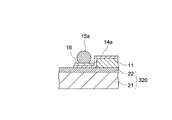
<第1の実施形態>
図1および図2は、本発明の一実施形態に係るラム波デバイスの構成を示す概略図であり、図1は平面図、図2は図1における[A]−[A]線方向の断面図である。各図においてX,YおよびZの各軸方向は、相互に直交する3軸方向を示しており、Z軸方向はラム波デバイスの厚み方向(高さ方向)に相当する。
<First Embodiment>
1 and 2 are schematic views showing the configuration of a Lamb wave device according to an embodiment of the present invention. FIG. 1 is a plan view, and FIG. 2 is a cross section in the [A]-[A] line direction in FIG. FIG. In each figure, the axial directions of X, Y, and Z indicate three axial directions orthogonal to each other, and the Z-axis direction corresponds to the thickness direction (height direction) of the Lamb wave device.
[全体構成]
本実施形態のラム波デバイス100は、圧電機能層110と、支持体120とを有する。本実施形態においてラム波デバイス100は、携帯機器の送受信用フィルタに用いられるラム波型共振器として構成される。
[overall structure]
The
圧電機能層110は、圧電基板11と、IDT電極12とを有する。支持体120は、支持基板21と、接合層22とを有する。支持体120は、IDT電極12で励振可能に圧電基板11を支持する。以下、各部の詳細について説明する。
The piezoelectric
(圧電基板)
圧電基板11は、圧電材料で構成され、本実施形態では、タンタル酸リチウム(LT)、ニオブ酸リチウム(LN)等の圧電性単結晶材料が用いられる。これ以外にも、圧電材料として、窒化アルミニウム(AlN)や酸化亜鉛(ZnO)、チタン酸ジルコン酸鉛(PZT)等が適用可能である。圧電基板11の厚みは特に限定されず、本実施形態では約1μmである。
(Piezoelectric substrate)
The
圧電基板11は、典型的には、所定厚みの基板を研磨等により薄化処理して形成されるが、これ以外にも、スパッタリング法等で成膜された圧電薄膜で構成されてもよい。
The
(IDT電極)
IDT電極12は、圧電基板11の表面11A(第1の面)に配置され、一対の櫛形電極12a,12bを有する。櫛形電極12a,12bは、それぞれ複数の電極指13a,13bを有し、一方の電極指13aと他方の電極指13bとが所定の間隔をおいて交互に配列するように相互に対向して配置されている。電極指13a,13bの間隔(電極ピッチp)は、圧電基板11の厚み、励振されるラム波の伝播速度、圧電機能層110の共振周波数等に応じて設定される。電極指13a,13bの数は図示の例に限られず、より多くの本数で構成されてもよい。
(IDT electrode)
The
電極ピッチpは、典型的には、励振されるラム波の波長の2分の1(λ/2)とされる。ラム波デバイス100(圧電機能層110)の共振周波数Fr[Hz]は、ラム波の波長および伝播速度(位相速度)をそれぞれλ[m]およびV[m/s]としたとき、
Fr=V/λ …(1)
の関係を満たす。
The electrode pitch p is typically set to half the wavelength of the excited Lamb wave (λ / 2). The resonance frequency Fr [Hz] of the Lamb wave device 100 (piezoelectric functional layer 110) is obtained when the wavelength and propagation velocity (phase velocity) of the Lamb wave are λ [m] and V [m / s], respectively.
Fr = V / λ (1)
Satisfy the relationship.
一方、ラム波の伝播速度は圧電基板が薄くなるほど大きくなり、高次モードであるほどその傾向が顕著となる。ラム波の伝播速度は、通常、圧電基板の厚みと波長との比である板厚比(厚み/波長)との関係で表される。一例として、128Y(128°回転Yカット)−LN基板の位相速度特性を図3に示す。この例では、板厚比0.2のときのラム波(A1モード)の位相速度は、13072[m/s]となる。 On the other hand, the propagation speed of the Lamb wave increases as the piezoelectric substrate becomes thinner, and the tendency becomes more remarkable as the mode is higher. The propagation speed of the Lamb wave is usually represented by a relationship with a plate thickness ratio (thickness / wavelength) which is a ratio between the thickness of the piezoelectric substrate and the wavelength. As an example, FIG. 3 shows the phase velocity characteristics of a 128Y (128 ° rotated Y-cut) -LN substrate. In this example, the phase velocity of the Lamb wave (A1 mode) when the plate thickness ratio is 0.2 is 13072 [m / s].
IDT電極12を構成する一対の櫛形電極12a,12bのうち、一方の櫛形電極は例えば入出力端子に接続され、他方の櫛形電極は例えばグランド端子に接続される。図示せずとも圧電機能層110は、IDT電極12で励振されたラム波を反射する反射器を有してもよい。この場合、反射器は、IDT電極12を挟むように、IDT電極12の両側にそれぞれ配置される。
Of the pair of
(支持体)
支持体120は、圧電機能層110を支持する支持基板21と、圧電機能層110と支持基板21との間を接合する接合層22とを有する。
(Support)
The
支持基板21は、圧電機能層110を支持できる適度な強度あるいは剛性を有する材料で形成される。このような材料として、典型的には、シリコンが採用されるが、これ以外にも、金属、ガラス、サファイア、プラスチック等の各種材料を採用することが可能である。支持基板21の厚みは例えば約300μmである。
The
接合層22は、典型的には接着剤が適用可能であり、これ以外にも、金属ろう材、粘着テープ等の各種材料が適用可能である。接着剤としては、紫外線硬化樹脂、熱硬化性樹脂、熱可塑性樹脂、感圧型接着剤等が用いられる。
An adhesive can be typically applied to the
接合層22は、支持体120の支持面201を形成し、圧電基板11の表面11Aに対向する裏面11B(第2の面)と接合される。接合層22は、矩形の環状に形成される。これにより圧電基板11の裏面11B、支持基板21の表面および接合層22の内周面で区画されたキャビティ部23が形成される。
The
キャビティ部23は、支持面201に隣接して設けられ、圧電基板11を介してIDT電極12と対向する。すなわちキャビティ部23は、圧電基板11を所定の共振周波数で振動させるための自由空間を形成する。キャビティ部23と対向する圧電基板11の領域を圧電基板11の第1の領域111としたとき、この第1の領域111の表面11A側にIDT電極12の電極指13a,13bがそれぞれ配置される。一方、第1の領域111を囲む環状の領域は圧電基板11の第2の領域112とされ、この第2の領域112は、支持体120(接合層22)によって支持される領域に相当する。
The
キャビティ部23の高さは接合層22の厚みで適宜の値に設定され、例えば1μmとされる。これ以外にも、接合層22で囲まれる支持基板21の表面領域に適度な深さの凹部が形成されてもよい。これによりキャビティ部23の高さを任意の大きさに調整することができる。
The height of the
接合層22は必要に応じて省略されてもよい。すなわち支持基板21は圧電基板11に直接的に接合されてもよい。この場合、支持基板21は支持体120を構成し、圧電基板11と接合される支持基板21の表面は支持体120の支持面201を形成する。また上記の場合、キャビティ部23は、支持基板21の表面に形成された凹所、開口または孔で構成される。
The
(切欠き部)
ラム波デバイスの共振周波数(Fr)は、(1)式で示したようにラム波の伝播速度(V)と波長(λ)によって定まり、波長(λ)は、IDT電極12の電極指13a,13bの電極ピッチp(図2)で設定される。すなわちラム波型共振素子の周波数特性は、圧電基板11の厚み、IDT電極の電極ピッチにそれぞれ独立に依存する。
しかしながら、圧電基板の厚みを精度よく管理することは容易ではなく、目的とする厚みの圧電基板を得るためには加工コストの増大と生産性の低下が避けられない。また圧電基板の厚みが面内でばらつくと、伝播速度(V)が変動し、所望の共振周波数が得られにくくなる。
そこで本実施形態では、圧電基板の厚みを実際に測定し、その実測値に応じてIDT電極の電極ピッチを調整することによって、目的とする共振周波数を有するラム波デバイスを得るようにしている。
(Notch)
The resonance frequency (Fr) of the Lamb wave device is determined by the propagation speed (V) and the wavelength (λ) of the Lamb wave as shown in the equation (1), and the wavelength (λ) is determined by the
However, it is not easy to accurately manage the thickness of the piezoelectric substrate, and in order to obtain a piezoelectric substrate having a target thickness, an increase in processing cost and a decrease in productivity are inevitable. Further, if the thickness of the piezoelectric substrate varies in the plane, the propagation speed (V) varies, making it difficult to obtain a desired resonance frequency.
Therefore, in the present embodiment, the thickness of the piezoelectric substrate is actually measured, and the electrode pitch of the IDT electrodes is adjusted according to the actually measured value, thereby obtaining a Lamb wave device having a target resonance frequency.
すなわち本実施形態のラム波デバイス100において、圧電機能層110は、切欠き部14を有する。切欠き部14は、圧電基板11に設けられ、圧電基板11の表面11Aと裏面11Bとの間を連絡する段差面140を含む。
That is, in the
本実施形態において切欠き部14は、圧電基板11の第2の領域112に設けられ、圧電基板11を貫通する貫通孔で構成される。したがって、支持体120の支持面201の一部は、切欠き部14を介して圧電基板11の表面側に露出される。
In the present embodiment, the
切欠き部14は、圧電基板11の厚みの測定に用いられる。切欠き部14は、圧電基板11の第2の領域112に形成されているため、切欠き部14の底部は支持体120の支持面201に対応し、したがって段差面140の高さ(切欠き部14の深さ)を測定することで、圧電基板11の厚みデータを精度よく取得することができる。その結果、圧電基板11の厚みから共振周波数のばらつきの予測および調整すべき量の把握が可能となり、これらに応じてIDT電極12の電極ピッチpを設定することにより、作製されるラム波型共振素子のばらつきを抑えることが可能となる。
The
本実施形態においては、切欠き部14の段差面140を触針式段差計で測定することで、圧電基板11の厚みが測定される。これにより支持面201の光学的性質に依存することなく圧電基板11の高精度な厚み測定が可能となる。
In the present embodiment, the thickness of the
例えば光干渉式段差計を用いて切欠き部の深さを測定する場合、切欠き部から露出する支持体の表面が透明体や樹脂の場合には光の透過、吸収等により所定以上の反射光強度が得られにくくなり、精度の高い段差測定が不可能となる。一方、触針式段差計によれば、支持体の光学特性に影響されることなく高精度な段差測定が可能となる。 For example, when measuring the depth of a notch using an optical interferometer, if the surface of the support exposed from the notch is a transparent body or resin, it will reflect more than a predetermined amount due to light transmission, absorption, etc. It becomes difficult to obtain the light intensity, and it becomes impossible to measure the level difference with high accuracy. On the other hand, according to the stylus type step meter, it is possible to measure the step with high accuracy without being affected by the optical characteristics of the support.
切欠き部14の開口部は略矩形に形成されるが、これに限られず、その他の幾何学形状で形成されてもよい。例えば、切欠き部14の開口部は、円、楕円、長円等のように一部に円弧を含む形状や、星型、十字形状等のようなシンボリックな形状に形成されてもよい。切欠き部14の開口部の大きさ(開口幅)は、段差計の触針が切欠き部14の内部に進入可能な大きさであれば特に限定されず、例えば30μm以上とされる。
The opening of the
切欠き部14の形成方法は特に限定されず、エッチング、レーザ加工、機械加工等の各種表面加工技術が適用可能である。切欠き部14の段差面140は、加工方法によって異なる形態を有するが、図4(A)に示すように圧電基板11の表面に対して垂直な段差面141であってもよいし、図4(B)に示すように所定の角度で傾斜するテーパ状の段差面142であってもよい。
The formation method of the
なお加工方法によっては、垂直状の段差面141よりもテーパ状の段差面142の方が好ましい場合がある。例えば、LT基板またはLN基板をドライエッチング法によって段差面が垂直な開口部を形成する場合、開口部の周縁部にエッチング反応物が再堆積(リデポ)する場合がある。この場合、上記周縁部の付着物を原因として当該開口部の段差を精度よく測定することが困難になる。一方、このような基板に段差面がテーパ状の開口部を形成する場合、開口部の周縁部への再堆積物の付着を抑制でき、段差の測定精度を高めることができる。
Depending on the processing method, the
なおまた、加工方法によって切欠き部14の段差面の表面性状が変化する。例えば、ダイサーによる加工では、加工面が粗くなり、開口部周縁のチッピングも起こり易い。この場合、高精度な段差測定が困難となる。一方、ドライエッチング加工によれば、加工面を比較的平滑にでき、開口部周縁のチッピングも起こりにくい。このため高精度な段差測定が可能となり、圧電基板11の厚みを精度よく測定することができる。
In addition, the surface property of the stepped surface of the
切欠き部14の位置は特に限定されないが、IDT電極12の近傍に切欠き部14が設けられることで、IDT電極12の配置領域の圧電基板11の厚みを高精度に測定することができる。また、切欠き部14が第2の領域112に形成されることで、第1の領域111を伝播するラム波デバイス100の伝播特性への影響を防ぐことができる。
The position of the
本実施形態のラム波デバイス100は、複数の切欠き部14を有する。図1および図2に示すように、複数の切欠き部14は、IDT電極12を挟むように圧電基板11の第2の領域112にそれぞれ設けられる。これにより圧電基板11の厚みをより高精度に測定することができるとともに、厚みバラツキを考慮したIDT電極の電極ピッチの調整が可能となる。
The
複数の切欠き部14各々は、相互に同一の形状であってもよいし、異なる形状であってもよい。また大きさも特に限定されず、個々の切欠き部14の形状や位置等に応じて適宜設定可能である。
Each of the plurality of
以上のように本実施形態のラム波デバイス100においては、圧電基板11の表面11Aと裏面11Bとの間を連絡する段差面140(141,142)を含む切欠き部14が圧電基板11に設けられているため、当該段差面を利用して圧電基板11の厚みを高精度に測定することが可能となる。これにより所望とする共振特性を有するラム波デバイスを安定して製造することができる。
As described above, in the
[製造方法]
次に、以上のように構成されるラム波デバイス100の製造方法について説明する。本実施形態においてラム波デバイス100は、ウェーハレベルで複数個の素子が同時に作製され、作製後は素子毎に個片化(チップ化)される。
[Production method]
Next, a method for manufacturing the
図5(A)〜(F)は、本実施形態のラム波デバイス100の製造方法を説明する一素子当たりの概略工程断面図である。
5A to 5F are schematic process cross-sectional views for each element for explaining the method for manufacturing the
まず図5(A)に示すように、比較的厚いウェーハ状の圧電基板11Wを準備する。圧電基板11Wとしては、例えば、LT基板あるいはLN基板が用いられる。圧電基板11Wの厚みは特に限定されず、ハンドリングできる程度の適度の厚みが採用され、例えば0.3mmの圧電基板が用いられる。
First, as shown in FIG. 5A, a relatively thick wafer-like
次に、図5(B)に示すように、圧電基板11Wの裏面側に環状の接合層22が形成される。接合層22としては、例えば樹脂系接着材料が用いられる。厚みは、キャビティ部23を形成する上で必要な厚み(例えば1μm)とされる。
Next, as shown in FIG. 5B, an
続いて図5(C)に示すように、接合層22を介して圧電基板11Wが、同じくウェーハ状の支持基板21Wの表面に積層される。支持基板21Wとしては、例えば厚みが300μmのシリコン基板が用いられる。
Subsequently, as shown in FIG. 5C, the
次に図5(D)に示すように、圧電基板11Wが所定厚み(例えば1μm)に薄化される。これによりメンブレン構造の圧電基板11Wが作製される。圧電基板11Wの薄化処理には、典型的には、CMP(Chemical Mechanical Polishing)法が用いられる。
Next, as shown in FIG. 5D, the
続いて図5(E)に示すように、接合層22により支持される圧電基板11W上の領域(第2の領域112に、圧電基板11Wを貫通する切欠き部14が形成される。
Subsequently, as illustrated in FIG. 5E, a
本実施形態では、切欠き部14はドライエッチング法で形成される。エッチング装置としては、プラズマエッチング装置(アルバック社製NLD)が用いられ、エッチングガスとしてはC3F8とArとの混合ガスが用いられる。エッチング条件は特に限定されないが、一例を挙げると、プラズマ形成用の高周波電力は600W(13.56MHz)、基板バイアスは300W、処理圧力は0.66Pa、エッチングガス流量はArが80sccm、C3F8が20sccmとされる。
In the present embodiment, the
切欠き部14の形成に際しては、あらかじめ圧電基板11W上に所定のレジストパターンが形成され、このレジストパターンをマスクとして圧電基板11Wがエッチングされる。切欠き部14は、テーパ状の段差面142(図4(B)参照)が形成されるように加工されることで、切欠き部14の開口周縁部におけるエッチング材料の再堆積を抑制することができる。このような段差面142の形成方法として、例えば、レジスト開口部の大きさがエッチングの進行に応じて徐々に広がるようにレジストマスクを形成する方法が挙げられる。
When forming the
次に、形成された切欠き部14を利用して圧電基板11Wの厚みが測定される。
Next, the thickness of the
切欠き部14は圧電基板11Wを貫通し、かつ、切欠き部14の底部が接合層22で形成されているため、切欠き部14の段差(切欠き部14の深さ)は、圧電基板11Wの厚みに相当する。したがって切欠き部14の段差を測定することで、当該切欠き部14の形成位置における圧電基板11Wの厚みが測定される。
Since the
続いて、測定された圧電基板11Wの厚みに応じて設定された電極間隔(電極ピッチ)のIDT電極12が、圧電基板11Wの所定位置(第1の領域111)に形成される。これにより目的とする周波数特性を有するラム波デバイス100を作製することができる。
Subsequently,
具体的には、測定された圧電基板11Wの厚みから所望の周波数特性が得られるラム波の波長(λ)を試算する。IDT電極12の電極指13a,13b間の間隔(電極ピッチ)は2分の1波長(λ/2)に相当するため、算出された波長λから電極ピッチを決定することができる。
Specifically, the wavelength (λ) of the Lamb wave from which a desired frequency characteristic is obtained is calculated from the measured thickness of the
さらに、圧電基板11Wの面内の複数箇所に設けられた複数の切欠き部14を利用することで、圧電基板11Wの厚みの面内分布を知ることができる。これにより領域ごとに電極ピッチの異なる複数のIDT電極12を形成することが可能となる。
Furthermore, the in-plane distribution of the thickness of the
このような作用効果は、ウェーハレベルで素子を作製する際に、素子領域毎に最適な電極ピッチを設定することができる。あるいは、1素子領域に複数のIDT電極が配置されるラム波デバイスにおいては、IDT電極の配置領域毎に測定した圧電基板の厚みに基づいて領域毎に最適な電極ピッチを設定することができる。 Such an effect can set an optimum electrode pitch for each element region when an element is manufactured at the wafer level. Alternatively, in a Lamb wave device in which a plurality of IDT electrodes are arranged in one element region, an optimum electrode pitch can be set for each region based on the thickness of the piezoelectric substrate measured for each IDT electrode arrangement region.
上述したように圧電基板は研磨あるいは研削処理により所定厚み(例えば1μm)に薄化されるが、研磨ばらつきにより基板面内で厚みにばらつきが生じ易い。128Y−LN基板を例に挙げると、基板中心の厚みが1.0μm、基板外周部の厚みが0.8μmであったとする。共振周波数を3.5GHzに設定すると、基板中心の波長を2.95μm、基板外周の波長を3.95μmとすることで、A1モードのラム波の伝播速度は、図3に示したように基板中心で10320m/s、基板外周部で13825m/sとなる。このように所望のフィルタ特性を一枚の基板(ウェーハ)の中で実現することができる。 As described above, the piezoelectric substrate is thinned to a predetermined thickness (for example, 1 μm) by polishing or grinding treatment, but the thickness tends to vary in the substrate surface due to polishing variation. Taking a 128Y-LN substrate as an example, it is assumed that the thickness at the center of the substrate is 1.0 μm and the thickness at the outer peripheral portion of the substrate is 0.8 μm. When the resonance frequency is set to 3.5 GHz, the wavelength of the center of the substrate is 2.95 μm and the wavelength of the outer periphery of the substrate is 3.95 μm, so that the propagation speed of the A1 mode Lamb wave is as shown in FIG. 10320 m / s at the center and 13825 m / s at the outer peripheral portion of the substrate. Thus, desired filter characteristics can be realized in one substrate (wafer).
IDT電極12の作製方法は特に限定されない。例えば、圧電基板の表面に成膜した電極層の上にレジストパターンを形成し、そのレジストパターンをマスクとしてパターンエッチングする方法が採用可能である。あるいは、圧電基板の表面に形成したレジストマスクの上から電極層を成膜した後、上記レジストマスクを除去する方法(リフトオフ)が採用されてもよい。
The manufacturing method of the
IDT電極12は、例えば、Al、Al−Cu合金、Cu、Ru、Pt、Au、Ta、Ti,Cr等の金属材料で形成される。IDT電極12の厚みは特に限定されず、例えば0.2μmである。IDT電極12を構成する金属膜は、種々の方法で成膜可能であり、例えば、スパッタリング法、真空蒸着法、イオンプレーティング法等が適用可能である。この場合、切欠き部14にはIDT電極12の構成材料が残存していてもよいし、切欠き部14を覆うレジストマスクを作製してIDT電極12が作製されてもよい。
The
IDT電極12の成膜後、必要な後処理を実施される。そして圧電基板11Wが各々の素子領域毎にダイシング(個片化)される。後処理としては、外部接続端子の形成、保護膜の形成等が挙げられる。
After the
以上のようにしてラム波デバイス100が作製される。本実施形態によれば、切欠き部14を用いて測定された圧電基板11の厚みに応じてIDT電極12の電極ピッチを決定するため、目的とする共振周波数を有するラム波デバイスを安定に製造することができる。
The
<第2の実施形態>
図6および図7は、本発明の第1の実施形態に係るラム波デバイスの構成を示す概略図である。図6はウェーハレベルにおける隣接する2つの素子領域を示す平面図であり、図7は図6における[B]−[B]線方向の断面図である。また図8はウェーハ状態の圧電基板の平面図である。
<Second Embodiment>
6 and 7 are schematic views showing the configuration of the Lamb wave device according to the first embodiment of the present invention. FIG. 6 is a plan view showing two adjacent element regions at the wafer level, and FIG. 7 is a cross-sectional view in the [B]-[B] line direction in FIG. FIG. 8 is a plan view of the piezoelectric substrate in a wafer state.
各図においてX,YおよびZの各軸方向は、相互に直交する3軸方向を示しており、Z軸方向はラム波デバイスの厚み方向(高さ方向)に相当する。以下、第1の実施形態と異なる構成について主に説明し、上述の実施形態と同様の構成については同様の符号を付しその説明を省略または簡略化する。 In each figure, the axial directions of X, Y, and Z indicate three axial directions orthogonal to each other, and the Z-axis direction corresponds to the thickness direction (height direction) of the Lamb wave device. Hereinafter, configurations different from those of the first embodiment will be mainly described, and configurations similar to those of the above-described embodiment will be denoted by the same reference numerals, and description thereof will be omitted or simplified.
本実施形態のラム波デバイス200は、圧電機能層210と、支持体220とを有する。圧電機能層210は、圧電基板11W(11)と、IDT電極12と、切欠き部24とを有する。
The
切欠き部24は、第1の実施形態と同様に、圧電基板11Wの厚みを測定し、IDT電極12の電極ピッチpを試算するために用いられる。切欠き部24は、直線的な溝部又は段部で形成され、圧電基板11Wの第2の領域112に形成される。本実施形態において切欠き部24は、隣接する複数のラム波デバイス200の間の境界部に沿って形成され、より具体的には、ダイシングラインLに沿って形成される。
The
切欠き部24は、圧電基板11の表面と裏面との間を連絡する段差面240を含む。切欠き部24は、例えばドライエッチング法で形成され、段差面240は例えばテーパ状に形成される。
The
切欠き部24は、ダイシングブレード(ダイシングソー)の幅よりも大きな幅で形成される。例えば30μm幅のブレードを使用してダイシングする場合、切欠き部24の幅は例えば50μm程度に設定される。これにより、ダイシング時における圧電基板11Wの破損を抑制することができる。図9(A),(B)は、ダイシング前後における圧電基板11Wと支持基板21Wとの積層基板を示す要部の拡大断面図である。
The
なお切欠き部24はダイシングラインLの役割も兼ねるため、圧電基板11Wの表面11Aの全域にわたって形成されるが、支持体220に支持されているため圧電基板11Wの強度の低下は問題にならない。
Since the
本実施形態においては、ダイシングラインLに沿うように切欠き部24が形成されているため、素子領域の全周における任意の位置において圧電基板11Wの厚み測定が可能となる。これによりIDT電極12の電極ピッチを高精度に測定することができる。
In the present embodiment, since the
以上のように構成される本実施形態のラム波デバイス200においても上述の第1の実施形態と同様の作用効果を得ることができる。すなわち本実施形態においても、切欠き部24が圧電基板11W(11)に設けられているため、その段差面240を利用して圧電基板11W(11)の厚みを高精度に測定することが可能となる。これにより所望とする共振特性を有するラム波デバイスを安定して製造することができる。
Also in the
<第3の実施形態>
図10および図12は、本発明の第3の実施形態に係るラム波デバイスの構成を示す概略図である。図10はウェーハレベルにおける隣接する2つの素子領域を示す平面図であり、図11は図10における[C]−[C]線方向の断面図である。また図12は上記ラム波デバイスの要部拡大断面図である。
<Third Embodiment>
10 and 12 are schematic views showing the configuration of a Lamb wave device according to the third embodiment of the present invention. FIG. 10 is a plan view showing two adjacent element regions at the wafer level, and FIG. 11 is a cross-sectional view in the [C]-[C] line direction in FIG. FIG. 12 is an enlarged cross-sectional view of the main part of the Lamb wave device.
各図においてX,YおよびZの各軸方向は、相互に直交する3軸方向を示しており、Z軸方向はラム波デバイスの厚み方向(高さ方向)に相当する。以下、第1の実施形態と異なる構成について主に説明し、上述の実施形態と同様の構成については同様の符号を付しその説明を省略または簡略化する。 In each figure, the axial directions of X, Y, and Z indicate three axial directions orthogonal to each other, and the Z-axis direction corresponds to the thickness direction (height direction) of the Lamb wave device. Hereinafter, configurations different from those of the first embodiment will be mainly described, and configurations similar to those of the above-described embodiment will be denoted by the same reference numerals, and description thereof will be omitted or simplified.
本実施形態のラム波デバイス300は、圧電機能層310と、支持体320とを有する。圧電機能層310は、圧電基板11W(11)と、IDT電極12と、切欠き部34とを有する。
The
切欠き部34は、第1の実施形態と同様に、圧電基板11Wの厚みを測定し、IDT電極12の電極ピッチpを試算するために用いられる。切欠き部34は、直線的な溝部又は段部で形成され、圧電基板11Wの第2の領域112に形成される。本実施形態において切欠き部34は、相互に隣接する2つのラム波デバイス300の境界部に設けられ、一方のラム波デバイス300のIDT電極12(櫛形電極12a)と他方のラム波デバイス300のIDT電極12(櫛形電極12b)との間を連絡するように帯状に形成される。
The
切欠き部34は、圧電基板11の表面と裏面との間を連絡する段差面340を含む。切欠き部34は、例えばドライエッチング法で形成され、段差面340は例えばテーパ状に形成される。
The
外部接続端子15a,15bは、櫛形電極12a,12bの上面と切欠き部34の底部(支持層22の表面)との間を連絡する引出し配線14a,14bの上にそれぞれ設けられる。引出し配線14a,14bは、例えば、Al、Al−Cu合金、Cu、Ru、Pt、Au、Ta、Ti,Cr等の金属材料で形成される。外部接続端子15a,15bは、例えばAuのスタッドバンプ、ボールバンプあるいはウェッジバンプで構成される。図12に示すように引出し配線14a,14bと外部接続端子15a,15bとの間にはTi/Au層等の下地層16が設けられてもよい。これにより両者間の密着性を高めることができる。
The
切欠き部34は、圧電基板11Wを貫通する深さで形成される。したがって切欠き部34からは圧電基板11Wの下地層である支持体320(接合層22)の表面が露出する。外部接続端子15a,15bは、この露出した支持体320の表面上に形成されるため、外部接続端子15a,15bの作製時あるいは外部の回路基板への実装時において圧電基板11Wに作用する外力あるいは機械的衝撃を緩和し、圧電基板11W(11)の損壊を防止することができる。
The
すなわち、外部接続端子15a,15bの作製にボンディングツール(キャピラリ)が使用される場合、バンプは下地基板上に押し付けられて形成されることになる。本実施形態においては外部接続端子15a,15bが切欠き部34底部の支持体320で支持されているため、外部接続端子15a,15bの作製時に圧電基板11Wにボンディングツールから荷重を受けることはなく、これにより圧電基板11Wの損壊を防止することができる。
That is, when a bonding tool (capillary) is used for manufacturing the
また、外部接続端子15a,15bはフリップチップ方式で外部の回路基板上に実装される場合、マウンタ(実装機)からの押圧力が素子に作用する。本実施形態においては外部接続端子15a,15bが切欠き部34底部の支持体320で支持されているため、実装荷重が直接圧電基板11に作用することが回避され、これにより圧電基板11の損壊を抑制することが可能となる。
Further, when the
<第4の実施形態>
図13および図14は、本発明の第4の実施形態に係るラム波デバイスの構成を示す概略図であり、図13は平面図、図14は図13における[D]−[D]線方向の断面図である。以下、第1の実施形態と異なる構成について主に説明し、上述の実施形態と同様の構成については同様の符号を付しその説明を省略または簡略化する。
<Fourth Embodiment>
13 and 14 are schematic views showing the configuration of a Lamb wave device according to the fourth embodiment of the present invention. FIG. 13 is a plan view, and FIG. 14 is the [D]-[D] line direction in FIG. FIG. Hereinafter, configurations different from those of the first embodiment will be mainly described, and configurations similar to those of the above-described embodiment will be denoted by the same reference numerals, and description thereof will be omitted or simplified.
本実施形態のラム波デバイス400は、切欠き部14の内部に充填材44が充填されている点で第1の実施形態と異なる。本実施形態のラム波デバイス400によれば、温度変化による圧電基板の膨張あるいは収縮を抑制し、共振周波数の温度依存特性を緩和することができる。
The
充填材44としては、例えばSiO2のように、圧電基板11よりも熱膨張係数が小さい材料が用いられる。圧電基板11がLT基板で構成される場合、熱負荷によるLT基板の熱膨張を抑制し、温度による特性変動を抑えるという効果がある。充填材44としては、SiO2に限られず、例えば、SiN等が採用可能である。
As the
特に本実施形態においては、切欠き部14はIDT電極12の両側に設けられ、充填材44はラム波の伝播方向に埋め込まれる。これにより温度補償効果を高めることができる。
In particular, in the present embodiment, the
図15は、切欠き部14への充填材44の充填方法を説明する概略工程図である。図15(A)に示すように切欠き部14を利用した圧電基板11の厚み測定を終了した後、圧電基板11の表面全域にSiO2膜44Fを形成する(図15(B))。その後、圧電基板11の表面を研磨することにより、切欠き部14内に充填材44が充填される(図15(C))。
FIG. 15 is a schematic process diagram for explaining a method of filling the
上述の第3および第4の実施形態は、圧電基板11の厚み測定のために形成された切欠き部14,34が、IDT電極12の形成後は別の構造部として機能させることができる。また第2から第4の実施形態に係るラム波デバイスは、第1の実施形態と同様な工程によって作製することができる。
In the third and fourth embodiments described above, the
以上、本発明の実施形態について説明したが、本発明は上述の実施形態にのみ限定されるものではなく、本発明の要旨を逸脱しない範囲内において種々変更を加え得ることは勿論である。 The embodiment of the present invention has been described above, but the present invention is not limited to the above-described embodiment, and it is needless to say that various modifications can be made without departing from the gist of the present invention.
例えば以上の各実施形態では、圧電基板を支持する支持体が支持基板21と接合層22とで構成されたが、これに限られず、例えば図16および図17に示した素子構造が採用されてもよい。
For example, in each of the above-described embodiments, the support body that supports the piezoelectric substrate is configured by the
図16は、支持体のキャビティ部が支持基板の貫通孔で形成されたラム波デバイスの製造方法を説明する概略工程断面図である。所定厚みの圧電基板51が支持体50の表面に積層された後、圧電基板51が所定厚みに薄化される(図16(A),(B))。次に、圧電基板51の所定位置に基板厚み測定用の切欠き部54と、測定された厚みに応じて電極ピッチが調整されたIDT電極52とが順次、形成される(図16(C),(D))。その後、IDT電極52直下の支持体50内にキャビティ部53が形成された後、キャビティ部53を被覆するカバー55が支持体50の裏面に接合される(図16(E),(F))。
FIG. 16 is a schematic process cross-sectional view illustrating a method for manufacturing a Lamb wave device in which a cavity portion of a support is formed by a through hole of a support substrate. After the
図17は、支持基板60表面の接合層67に犠牲層66を埋め込んだ後、犠牲層66を溶解除去して形成されたキャビティ部63を有するラム波デバイスの製造方法を説明する概略工程断面図である。犠牲層66は圧電基板61の裏面に形成され、支持基板60への積層時に接合層67の内部へ犠牲層66が埋め込まれる(図17(A),(B))。次に、圧電基板61が所定厚みに薄化された後、基板厚み測定用の切欠き部64が形成される(図17(C),(D))。このとき切欠き部64は、一部が犠牲層66に達するように形成される。そして切欠き部64を用いた圧電基板61の厚み測定結果に基づいてIDT電極62を作製した後、切欠き部64を介して犠牲層66を溶解除去する(図17(E),(F))。
FIG. 17 is a schematic cross-sectional process diagram illustrating a method for manufacturing a Lamb wave device having a
また図18に示すように、IDT電極12の周囲に複数の円形の切欠き部74が形成されてもよく、このような構成によっても上述と同様の作用効果を得ることができる。
Further, as shown in FIG. 18, a plurality of
11…圧電基板
12…IDT電極
14,24,34,44…切欠き部
15a,15b…外部接続端子
21…支持基板
22…接合層
23…キャビティ部
44…充填材
100,200,300,400…ラム波デバイス
110…圧電機能層
120…支持体
201…支持面
DESCRIPTION OF
Claims (11)
前記第2の面に接合され前記切欠き部を介して前記第1の面側に露出する支持面と、前記支持面に隣接して設けられ前記圧電基板を介して前記IDT電極と対向するキャビティ部と、を有する支持体と、
を具備し、
前記切欠き部は、前記支持面のみを露出させ、前記キャビティ部と連絡しないことを特徴とするラム波デバイス。 A piezoelectric substrate having a first surface and a second surface opposite to the first surface; an IDT electrode disposed on the first surface; the first surface provided on the piezoelectric substrate; A piezoelectric functional layer having a notch including a stepped surface communicating with the second surface;
A support surface that is bonded to the second surface and exposed to the first surface side through the notch, and a cavity that is provided adjacent to the support surface and faces the IDT electrode through the piezoelectric substrate A support having a portion;
Comprising
The notch portion exposes only the support surface and does not communicate with the cavity portion.
前記第1の面は、前記キャビティ部と対向する第1の領域と、前記第1の領域の外側を囲む第2の領域とを有し、
前記IDT電極は、前記第1の領域に配置され、
前記切欠き部は、前記第2の領域に設けられる
ラム波デバイス。 A lamb wave device according to claim 1,
The first surface includes a first region facing the cavity portion, and a second region surrounding the outside of the first region,
The IDT electrode is disposed in the first region,
The notch is a Lamb wave device provided in the second region.
前記切欠き部は、円形の開口部を有する貫通孔であり、
前記第1の面に垂直な方向から見て、前記切欠き部は前記IDT電極に対し、前記IDT電極の電極指の配列方向に対し垂直方向に位置することを特徴とするラム波デバイス。 The Lamb wave device according to claim 1 or 2,
The notch is a through hole having an opening of a circular shape,
The Lamb wave device, wherein the notch portion is positioned perpendicular to the IDT electrode in the direction perpendicular to the first surface with respect to the arrangement direction of the electrode fingers of the IDT electrode.
前記貫通孔は30μm以上の開口幅を有する
ラム波デバイス。 A lamb wave device according to claim 3,
The through-hole has a Lamb wave device having an opening width of 30 μm or more.
前記切欠き部は、直線的な溝部又は段部であり、
前記切欠き部の、前記IDT電極の電極指の配列方向に対し垂直方向における長さは、前記電極指の前記垂直方向における長さよりも短いことを特徴とするラム波デバイス。 The Lamb wave device according to claim 1 or 2,
The notch is a linear groove or step,
A Lamb wave device, wherein a length of the notch portion in a direction perpendicular to an arrangement direction of the electrode fingers of the IDT electrode is shorter than a length of the electrode finger in the vertical direction.
前記切欠き部は、複数の切欠き部を含み、
前記複数の切欠き部は、前記圧電基板上の複数の位置に設けられる
ラム波デバイス。 The lamb wave device according to any one of claims 1 to 5,
The notch includes a plurality of notches,
The plurality of notches are provided at a plurality of positions on the piezoelectric substrate.
前記第2の面に接合され前記切欠き部を介して前記第1の面側に露出する支持面と、前記支持面に隣接して設けられ前記圧電基板を介して前記IDT電極と対向するキャビティ部と、を有する支持体と、
前記切欠き部に配置され、前記IDT電極と電気的に接続される外部接続端子と
を具備するラム波デバイス。 A piezoelectric substrate having a first surface and a second surface opposite to the first surface; an IDT electrode disposed on the first surface; the first surface provided on the piezoelectric substrate; A piezoelectric functional layer having a notch including a stepped surface communicating with the second surface;
A support surface that is bonded to the second surface and exposed to the first surface side through the notch, and a cavity that is provided adjacent to the support surface and faces the IDT electrode through the piezoelectric substrate A support having a portion;
A lamb wave device comprising: an external connection terminal disposed in the notch and electrically connected to the IDT electrode.
前記第2の面に接合され前記切欠き部を介して前記第1の面側に露出する支持面と、前記支持面に隣接して設けられ前記圧電基板を介して前記IDT電極と対向するキャビティ部と、を有する支持体と
を具備するラム波デバイス。 A piezoelectric substrate having a first surface and a second surface opposite to the first surface; an IDT electrode disposed on the first surface; the first surface provided on the piezoelectric substrate; A piezoelectric functional layer having a notch portion including a stepped surface communicating with the second surface, and a filling layer in which the notch portion is filled with a material having a smaller thermal expansion coefficient than the piezoelectric substrate;
A support surface that is bonded to the second surface and exposed to the first surface side through the notch, and a cavity that is provided adjacent to the support surface and faces the IDT electrode through the piezoelectric substrate A lamb wave device.
前記支持面は、前記支持体に設けられた接着材料層を含む
ラム波デバイス。 The lamb wave device according to any one of claims 1 to 8,
The support surface includes an adhesive material layer provided on the support.
前記切欠き部を利用して前記圧電基板の厚みを測定し、
前記圧電基板の厚みに応じて設定された電極間隔のIDT電極を前記圧電基板の表面に形成する
ラム波デバイスの製造方法。 Form a notch in a piezoelectric substrate with a predetermined thickness laminated on the support,
Measure the thickness of the piezoelectric substrate using the notch,
A method of manufacturing a Lamb wave device, wherein IDT electrodes having an electrode interval set according to the thickness of the piezoelectric substrate are formed on the surface of the piezoelectric substrate.
前記切欠き部を形成する工程は、前記切欠き部をドライエッチング法で形成する
ラム波デバイスの製造方法。 A method for manufacturing a Lamb wave device according to claim 10,
The step of forming the notch includes forming the notch by a dry etching method.
Priority Applications (3)
| Application Number | Priority Date | Filing Date | Title |
|---|---|---|---|
| JP2012150295A JP6092535B2 (en) | 2012-07-04 | 2012-07-04 | Lamb wave device and manufacturing method thereof |
| CN201310130405.2A CN103532513A (en) | 2012-07-04 | 2013-04-16 | Lamb wave device and manufacturing method thereof |
| US13/911,994 US9634226B2 (en) | 2012-07-04 | 2013-06-06 | Lamb wave device and manufacturing method thereof |
Applications Claiming Priority (1)
| Application Number | Priority Date | Filing Date | Title |
|---|---|---|---|
| JP2012150295A JP6092535B2 (en) | 2012-07-04 | 2012-07-04 | Lamb wave device and manufacturing method thereof |
Publications (2)
| Publication Number | Publication Date |
|---|---|
| JP2014013991A JP2014013991A (en) | 2014-01-23 |
| JP6092535B2 true JP6092535B2 (en) | 2017-03-08 |
Family
ID=49877988
Family Applications (1)
| Application Number | Title | Priority Date | Filing Date |
|---|---|---|---|
| JP2012150295A Expired - Fee Related JP6092535B2 (en) | 2012-07-04 | 2012-07-04 | Lamb wave device and manufacturing method thereof |
Country Status (3)
| Country | Link |
|---|---|
| US (1) | US9634226B2 (en) |
| JP (1) | JP6092535B2 (en) |
| CN (1) | CN103532513A (en) |
Families Citing this family (147)
| Publication number | Priority date | Publication date | Assignee | Title |
|---|---|---|---|---|
| JP6335492B2 (en) * | 2013-11-29 | 2018-05-30 | 太陽誘電株式会社 | Elastic wave element |
| DE112015001240B4 (en) * | 2014-03-14 | 2024-06-20 | Murata Manufacturing Co., Ltd. | Device for elastic waves |
| CN106489239B (en) * | 2014-07-07 | 2020-03-03 | 天工滤波方案日本有限公司 | Acoustic wave device, and antenna duplexer, module and communication device using the same |
| CN206878791U (en) * | 2014-12-08 | 2018-01-12 | 株式会社村田制作所 | Piezoelectric device |
| JP6800882B2 (en) * | 2014-12-17 | 2020-12-16 | コルボ ユーエス インコーポレイテッド | Plate wave device with wave confinement structure and manufacturing method |
| WO2016098526A1 (en) | 2014-12-18 | 2016-06-23 | 株式会社村田製作所 | Acoustic wave device and manufacturing method therefor |
| FR3037443B1 (en) | 2015-06-12 | 2018-07-13 | Soitec | HETEROSTRUCTURE AND METHOD OF MANUFACTURE |
| WO2017077892A1 (en) * | 2015-11-02 | 2017-05-11 | 株式会社村田製作所 | Acoustic wave device |
| WO2018100840A1 (en) * | 2016-11-29 | 2018-06-07 | 株式会社村田製作所 | Elastic wave device and method for manufacturing same, high-frequency front end circuit, and communication device |
| JP2019029941A (en) * | 2017-08-02 | 2019-02-21 | 株式会社ディスコ | Method for manufacturing substrate for acoustic wave device |
| CN109560784B (en) * | 2017-09-27 | 2021-09-24 | 中国科学院半导体研究所 | Lamb wave resonator and method of making the same |
| US10911023B2 (en) | 2018-06-15 | 2021-02-02 | Resonant Inc. | Transversely-excited film bulk acoustic resonator with etch-stop layer |
| US11323089B2 (en) | 2018-06-15 | 2022-05-03 | Resonant Inc. | Filter using piezoelectric film bonded to high resistivity silicon substrate with trap-rich layer |
| US11996827B2 (en) | 2018-06-15 | 2024-05-28 | Murata Manufacturing Co., Ltd. | Transversely-excited film bulk acoustic resonator with periodic etched holes |
| US12040779B2 (en) | 2020-04-20 | 2024-07-16 | Murata Manufacturing Co., Ltd. | Small transversely-excited film bulk acoustic resonators with enhanced Q-factor |
| US12237826B2 (en) | 2018-06-15 | 2025-02-25 | Murata Manufacturing Co., Ltd. | Transversely-excited film bulk acoustic resonator with optimized electrode thickness, mark, and pitch |
| US10491192B1 (en) * | 2018-06-15 | 2019-11-26 | Resonant Inc. | Transversely-excited film bulk acoustic resonator |
| US11206009B2 (en) | 2019-08-28 | 2021-12-21 | Resonant Inc. | Transversely-excited film bulk acoustic resonator with interdigital transducer with varied mark and pitch |
| US10601392B2 (en) | 2018-06-15 | 2020-03-24 | Resonant Inc. | Solidly-mounted transversely-excited film bulk acoustic resonator |
| US11323090B2 (en) | 2018-06-15 | 2022-05-03 | Resonant Inc. | Transversely-excited film bulk acoustic resonator using Y-X-cut lithium niobate for high power applications |
| US10637438B2 (en) | 2018-06-15 | 2020-04-28 | Resonant Inc. | Transversely-excited film bulk acoustic resonators for high power applications |
| US11936358B2 (en) * | 2020-11-11 | 2024-03-19 | Murata Manufacturing Co., Ltd. | Transversely-excited film bulk acoustic resonator with low thermal impedance |
| US11323096B2 (en) | 2018-06-15 | 2022-05-03 | Resonant Inc. | Transversely-excited film bulk acoustic resonator with periodic etched holes |
| US12088281B2 (en) | 2021-02-03 | 2024-09-10 | Murata Manufacturing Co., Ltd. | Transversely-excited film bulk acoustic resonator with multi-mark interdigital transducer |
| US11509279B2 (en) | 2020-07-18 | 2022-11-22 | Resonant Inc. | Acoustic resonators and filters with reduced temperature coefficient of frequency |
| US11146232B2 (en) | 2018-06-15 | 2021-10-12 | Resonant Inc. | Transversely-excited film bulk acoustic resonator with reduced spurious modes |
| TW201941464A (en) | 2018-03-02 | 2019-10-16 | 美商天工方案公司 | Lamb wave loop circuit for acoustic wave filter |
| WO2019167918A1 (en) * | 2018-03-02 | 2019-09-06 | 京セラ株式会社 | Composite substrate and piezoelectric element |
| US11329628B2 (en) | 2020-06-17 | 2022-05-10 | Resonant Inc. | Filter using lithium niobate and lithium tantalate transversely-excited film bulk acoustic resonators |
| US12040781B2 (en) | 2018-06-15 | 2024-07-16 | Murata Manufacturing Co., Ltd. | Transversely-excited film bulk acoustic resonator package |
| US12113512B2 (en) | 2021-03-29 | 2024-10-08 | Murata Manufacturing Co., Ltd. | Layout of XBARs with multiple sub-resonators in parallel |
| US10985728B2 (en) | 2018-06-15 | 2021-04-20 | Resonant Inc. | Transversely-excited film bulk acoustic resonator and filter with a uniform-thickness dielectric overlayer |
| US12132464B2 (en) | 2018-06-15 | 2024-10-29 | Murata Manufacturing Co., Ltd. | Filter using transversely-excited film bulk acoustic resonators with divided frequency-setting dielectric layers |
| US12081187B2 (en) | 2018-06-15 | 2024-09-03 | Murata Manufacturing Co., Ltd. | Transversely-excited film bulk acoustic resonator |
| US12218650B2 (en) | 2018-06-15 | 2025-02-04 | Murata Manufacturing Co., Ltd. | Transversely-excited film bulk acoustic resonator |
| US12170516B2 (en) | 2018-06-15 | 2024-12-17 | Murata Manufacturing Co., Ltd. | Filters using transversly-excited film bulk acoustic resonators with frequency-setting dielectric layers |
| US11996825B2 (en) | 2020-06-17 | 2024-05-28 | Murata Manufacturing Co., Ltd. | Filter using lithium niobate and rotated lithium tantalate transversely-excited film bulk acoustic resonators |
| US11888463B2 (en) | 2018-06-15 | 2024-01-30 | Murata Manufacturing Co., Ltd. | Multi-port filter using transversely-excited film bulk acoustic resonators |
| US11967945B2 (en) | 2018-06-15 | 2024-04-23 | Murata Manufacturing Co., Ltd. | Transversly-excited film bulk acoustic resonators and filters |
| US11909381B2 (en) | 2018-06-15 | 2024-02-20 | Murata Manufacturing Co., Ltd. | Transversely-excited film bulk acoustic resonators with two-layer electrodes having a narrower top layer |
| US12237827B2 (en) | 2018-06-15 | 2025-02-25 | Murata Manufacturing Co., Ltd. | Solidly-mounted transversely-excited film bulk acoustic filters with multiple piezoelectric plate thicknesses |
| US10992284B2 (en) | 2018-06-15 | 2021-04-27 | Resonant Inc. | Filter using transversely-excited film bulk acoustic resonators with multiple frequency setting layers |
| US12191838B2 (en) | 2018-06-15 | 2025-01-07 | Murata Manufacturing Co., Ltd. | Solidly-mounted transversely-excited film bulk acoustic device and method |
| US12191837B2 (en) | 2018-06-15 | 2025-01-07 | Murata Manufacturing Co., Ltd. | Solidly-mounted transversely-excited film bulk acoustic device |
| US12212306B2 (en) | 2018-06-15 | 2025-01-28 | Murata Manufacturing Co., Ltd. | Transversely-excited film bulk acoustic resonator with multiple diaphragm thicknesses and fabrication method |
| US12119808B2 (en) | 2018-06-15 | 2024-10-15 | Murata Manufacturing Co., Ltd. | Transversely-excited film bulk acoustic resonator package |
| US12149227B2 (en) | 2018-06-15 | 2024-11-19 | Murata Manufacturing Co., Ltd. | Transversely-excited film bulk acoustic resonator package |
| US11146238B2 (en) | 2018-06-15 | 2021-10-12 | Resonant Inc. | Film bulk acoustic resonator fabrication method |
| US11996822B2 (en) | 2018-06-15 | 2024-05-28 | Murata Manufacturing Co., Ltd. | Wide bandwidth time division duplex transceiver |
| US12095441B2 (en) | 2018-06-15 | 2024-09-17 | Murata Manufacturing Co., Ltd. | Transversely excited film bulk acoustic resonator with recessed interdigital transducer fingers |
| US11949402B2 (en) | 2020-08-31 | 2024-04-02 | Murata Manufacturing Co., Ltd. | Resonators with different membrane thicknesses on the same die |
| US11876498B2 (en) | 2018-06-15 | 2024-01-16 | Murata Manufacturing Co., Ltd. | Transversely-excited film bulk acoustic resonator with multiple diaphragm thicknesses and fabrication method |
| US12155374B2 (en) | 2021-04-02 | 2024-11-26 | Murata Manufacturing Co., Ltd. | Tiled transversely-excited film bulk acoustic resonator high power filters |
| US12463619B2 (en) | 2018-06-15 | 2025-11-04 | Murata Manufacturing Co., Ltd. | Filter device |
| US11323091B2 (en) * | 2018-06-15 | 2022-05-03 | Resonant Inc. | Transversely-excited film bulk acoustic resonator with diaphragm support pedestals |
| US11901878B2 (en) | 2018-06-15 | 2024-02-13 | Murata Manufacturing Co., Ltd. | Transversely-excited film bulk acoustic resonators with two-layer electrodes with a wider top layer |
| US10917072B2 (en) | 2019-06-24 | 2021-02-09 | Resonant Inc. | Split ladder acoustic wave filters |
| US12021496B2 (en) * | 2020-08-31 | 2024-06-25 | Murata Manufacturing Co., Ltd. | Resonators with different membrane thicknesses on the same die |
| US10826462B2 (en) | 2018-06-15 | 2020-11-03 | Resonant Inc. | Transversely-excited film bulk acoustic resonators with molybdenum conductors |
| US11870423B2 (en) | 2018-06-15 | 2024-01-09 | Murata Manufacturing Co., Ltd. | Wide bandwidth temperature-compensated transversely-excited film bulk acoustic resonator |
| US11349452B2 (en) | 2018-06-15 | 2022-05-31 | Resonant Inc. | Transversely-excited film bulk acoustic filters with symmetric layout |
| US10998882B2 (en) | 2018-06-15 | 2021-05-04 | Resonant Inc. | XBAR resonators with non-rectangular diaphragms |
| US12301212B2 (en) | 2018-06-15 | 2025-05-13 | Murata Manufacturing Co., Ltd. | XBAR resonators with non-rectangular diaphragms |
| US12184261B2 (en) | 2018-06-15 | 2024-12-31 | Murata Manufacturing Co., Ltd. | Transversely-excited film bulk acoustic resonator with a cavity having round end zones |
| US12155371B2 (en) | 2021-03-29 | 2024-11-26 | Murata Manufacturing Co., Ltd. | Layout of xbars with multiple sub-resonators in series |
| US11323095B2 (en) | 2018-06-15 | 2022-05-03 | Resonant Inc. | Rotation in XY plane to suppress spurious modes in XBAR devices |
| US12283944B2 (en) | 2018-06-15 | 2025-04-22 | Murata Manufacturing Co., Ltd. | Transversely-excited film bulk acoustic resonator with recessed rotated-Y-X cut lithium niobate |
| US12224732B2 (en) | 2018-06-15 | 2025-02-11 | Murata Manufacturing Co., Ltd. | Solidly-mounted transversely-excited film bulk acoustic resonators and filters for 27 GHz communications bands |
| US11349450B2 (en) | 2018-06-15 | 2022-05-31 | Resonant Inc. | Symmetric transversely-excited film bulk acoustic resonators with reduced spurious modes |
| US11264966B2 (en) | 2018-06-15 | 2022-03-01 | Resonant Inc. | Solidly-mounted transversely-excited film bulk acoustic resonator with diamond layers in Bragg reflector stack |
| US12375056B2 (en) | 2018-06-15 | 2025-07-29 | Murata Manufacturing Co., Ltd. | Transversely-excited film bulk acoustic resonators |
| US12244295B2 (en) | 2018-06-15 | 2025-03-04 | Murata Manufacturing Co., Ltd. | Transversely-excited film bulk acoustic resonators with two-layer electrodes having a narrower top layer |
| US12119805B2 (en) | 2018-06-15 | 2024-10-15 | Murata Manufacturing Co., Ltd. | Substrate processing and membrane release of transversely-excited film bulk acoustic resonator using a sacrificial tub |
| US11916539B2 (en) | 2020-02-28 | 2024-02-27 | Murata Manufacturing Co., Ltd. | Split-ladder band N77 filter using transversely-excited film bulk acoustic resonators |
| US12095446B2 (en) | 2018-06-15 | 2024-09-17 | Murata Manufacturing Co., Ltd. | Transversely-excited film bulk acoustic resonator with optimized electrode thickness, mark, and pitch |
| WO2020029153A1 (en) * | 2018-08-09 | 2020-02-13 | 天津大学 | Lamb wave resonator-based particle concentrator and operation method therefor |
| CN109450401B (en) * | 2018-09-20 | 2022-03-18 | 天津大学 | Flexible single crystal lamb wave resonator and method of forming the same |
| CN118573147A (en) | 2018-10-31 | 2024-08-30 | 株式会社村田制作所 | Solid-state assembly type transversely-excited film bulk acoustic resonator |
| JP7329954B2 (en) * | 2019-02-07 | 2023-08-21 | 太陽誘電株式会社 | Acoustic wave resonators, filters and multiplexers |
| DE112020001227T5 (en) | 2019-03-14 | 2022-02-10 | Resonant Inc. | Transversally excited acoustic film resonator with half-wave dielectric layer |
| DE102019109022A1 (en) | 2019-04-05 | 2020-10-08 | RF360 Europe GmbH | Surface acoustic wave resonator arrangement |
| CN118316415A (en) | 2019-04-05 | 2024-07-09 | 株式会社村田制作所 | Transverse excited film bulk acoustic resonator package and method |
| CN110995194B (en) * | 2019-12-30 | 2021-12-17 | 武汉敏声新技术有限公司 | Two-dimensional high-performance resonator |
| US11722116B2 (en) * | 2019-11-25 | 2023-08-08 | The Board Of Trustees Of The University Of Illinois | Acoustic resonators and filters that support fifth generation (5G) wireless communications standards |
| US11996820B2 (en) * | 2020-01-24 | 2024-05-28 | The Board Of Trustees Of The University Of Illinois | Fifth-generation (5G)-focused piezoelectric resonators and filters |
| US12255625B2 (en) | 2020-02-28 | 2025-03-18 | Murata Manufacturing Co., Ltd. | Filter using transversely-excited film bulk acoustic resonators with inductively coupled sub-resonators |
| JP6984800B1 (en) * | 2020-03-16 | 2021-12-22 | 株式会社村田製作所 | Elastic wave device |
| US12341493B2 (en) | 2020-04-20 | 2025-06-24 | Murata Manufacturing Co., Ltd. | Low loss transversely-excited film bulk acoustic resonators and filters |
| US12341490B2 (en) | 2020-04-20 | 2025-06-24 | Murata Manufacturing Co., Ltd. | Low loss transversely-excited film bulk acoustic resonators and filters |
| CN115428330B (en) * | 2020-04-29 | 2023-09-12 | 株式会社村田制作所 | elastic wave device |
| US11811391B2 (en) | 2020-05-04 | 2023-11-07 | Murata Manufacturing Co., Ltd. | Transversely-excited film bulk acoustic resonator with etched conductor patterns |
| US10992282B1 (en) | 2020-06-18 | 2021-04-27 | Resonant Inc. | Transversely-excited film bulk acoustic resonators with electrodes having a second layer of variable width |
| US11742828B2 (en) * | 2020-06-30 | 2023-08-29 | Murata Manufacturing Co., Ltd. | Transversely-excited film bulk acoustic resonator with symmetric diaphragm |
| US11817845B2 (en) | 2020-07-09 | 2023-11-14 | Murata Manufacturing Co., Ltd. | Method for making transversely-excited film bulk acoustic resonators with piezoelectric diaphragm supported by piezoelectric substrate |
| US11671070B2 (en) * | 2020-08-19 | 2023-06-06 | Murata Manufacturing Co., Ltd. | Transversely-excited film bulk acoustic resonators using multiple dielectric layer thicknesses to suppress spurious modes |
| WO2022059758A1 (en) * | 2020-09-16 | 2022-03-24 | 株式会社村田製作所 | Elastic wave device |
| US11476834B2 (en) | 2020-10-05 | 2022-10-18 | Resonant Inc. | Transversely-excited film bulk acoustic resonator matrix filters with switches in parallel with sub-filter shunt capacitors |
| US11405019B2 (en) | 2020-10-05 | 2022-08-02 | Resonant Inc. | Transversely-excited film bulk acoustic resonator matrix filters |
| US11658639B2 (en) | 2020-10-05 | 2023-05-23 | Murata Manufacturing Co., Ltd. | Transversely-excited film bulk acoustic resonator matrix filters with noncontiguous passband |
| US11728784B2 (en) | 2020-10-05 | 2023-08-15 | Murata Manufacturing Co., Ltd. | Transversely-excited film bulk acoustic resonator matrix filters with split die sub-filters |
| US11463066B2 (en) | 2020-10-14 | 2022-10-04 | Resonant Inc. | Transversely-excited film bulk acoustic resonators with piezoelectric diaphragm supported by piezoelectric substrate |
| US12003226B2 (en) | 2020-11-11 | 2024-06-04 | Murata Manufacturing Co., Ltd | Transversely-excited film bulk acoustic resonator with low thermal impedance |
| US12255617B2 (en) | 2020-11-11 | 2025-03-18 | Murata Manufacturing Co., Ltd. | Solidly-mounted transversely-excited film bulk acoustic resonators with low thermal impedance |
| US12255626B2 (en) | 2020-11-13 | 2025-03-18 | Murata Manufacturing Co., Ltd. | Solidly-mounted transversely-excited film bulk acoustic filters with excess piezoelectric material removed |
| US11496113B2 (en) * | 2020-11-13 | 2022-11-08 | Resonant Inc. | XBAR devices with excess piezoelectric material removed |
| US12028039B2 (en) * | 2020-11-13 | 2024-07-02 | Murata Manufacturing Co., Ltd. | Forming XBAR devices with excess piezoelectric material removed |
| US12362725B2 (en) | 2020-11-13 | 2025-07-15 | Murata Manufacturing Co., Ltd. | Transversely-excited film bulk acoustic filters with excess piezoelectric material removed |
| CN120200582A (en) * | 2020-11-13 | 2025-06-24 | 株式会社村田制作所 | Formation of an XBAR device with excess piezoelectric material removed |
| CN112688650A (en) * | 2020-12-17 | 2021-04-20 | 广东广纳芯科技有限公司 | Lamb wave resonator, and filter and electronic device provided with same |
| CN116686215A (en) * | 2020-12-22 | 2023-09-01 | 株式会社村田制作所 | elastic wave device |
| US12166468B2 (en) | 2021-01-15 | 2024-12-10 | Murata Manufacturing Co., Ltd. | Decoupled transversely-excited film bulk acoustic resonators for high power filters |
| US11239816B1 (en) | 2021-01-15 | 2022-02-01 | Resonant Inc. | Decoupled transversely-excited film bulk acoustic resonators |
| US12463615B2 (en) | 2021-01-21 | 2025-11-04 | Murata Manufacturing Co., Ltd | Transversely-excited film bulk acoustic resonators with improved coupling and reduced energy leakage |
| CN113210240B (en) * | 2021-03-23 | 2022-09-06 | 魔音智芯科技(深圳)有限公司 | Lamb wave device of double-sided interdigital transducer and preparation method thereof |
| US12348216B2 (en) | 2021-03-24 | 2025-07-01 | Murata Manufacturing Co., Ltd. | Acoustic filters with shared acoustic tracks and cascaded series resonators |
| CN117121380A (en) * | 2021-03-31 | 2023-11-24 | 株式会社村田制作所 | Elastic wave device |
| WO2022210293A1 (en) * | 2021-03-31 | 2022-10-06 | 株式会社村田製作所 | Elastic wave device |
| WO2022211087A1 (en) * | 2021-03-31 | 2022-10-06 | 株式会社村田製作所 | Elastic wave device |
| WO2022255482A1 (en) * | 2021-06-03 | 2022-12-08 | 株式会社村田製作所 | Elastic wave device |
| US12170513B2 (en) | 2021-06-30 | 2024-12-17 | Murata Manufacturing Co., Ltd. | Transversely-excited film bulk acoustic resonator with reduced substrate to contact bump thermal resistance |
| US12431857B2 (en) | 2021-06-30 | 2025-09-30 | Skyworks Solutions, Inc. | Acoustic wave device with acoustic obstruction structure |
| US20230039934A1 (en) * | 2021-07-14 | 2023-02-09 | The Board Of Trustees Of The University Of Illinois | Higher order lamb wave acoustic devices with complementarily-oriented piezoelectric layers |
| WO2023002822A1 (en) * | 2021-07-20 | 2023-01-26 | 株式会社村田製作所 | Elastic wave device and method for manufacturing same |
| US12456962B2 (en) | 2021-09-24 | 2025-10-28 | Murata Manufacturing Co., Ltd. | Transversely-excited film bulk acoustic resonators wafer-level packaging using a dielectric cover |
| US12451864B2 (en) | 2021-09-29 | 2025-10-21 | Murata Manufacturing Co., Ltd. | Transversely-excited film bulk acoustic resonators with curved shaped ends of fingers or opposing busbars |
| WO2023054675A1 (en) * | 2021-09-30 | 2023-04-06 | 株式会社村田製作所 | Acoustic wave device and method for manufacturing acoustic wave device |
| CN118044117A (en) * | 2021-09-30 | 2024-05-14 | 株式会社村田制作所 | Elastic wave device and method for manufacturing elastic wave device |
| WO2023058715A1 (en) * | 2021-10-07 | 2023-04-13 | 株式会社村田製作所 | Elastic wave device |
| CN118077144A (en) * | 2021-10-08 | 2024-05-24 | 株式会社村田制作所 | Elastic wave device and method for manufacturing elastic wave device |
| US12407326B2 (en) | 2021-11-04 | 2025-09-02 | Murata Manufacturing Co., Ltd. | Stacked die transversely-excited film bulk acoustic resonator (XBAR) filters |
| KR20230069710A (en) * | 2021-11-12 | 2023-05-19 | 삼성전자주식회사 | Directional acoustic sensor |
| WO2023090460A1 (en) * | 2021-11-22 | 2023-05-25 | 株式会社村田製作所 | Method for manufacturing acoustic wave device |
| CN118369853A (en) * | 2021-12-07 | 2024-07-19 | 株式会社村田制作所 | Elastic wave device |
| EP4199687B1 (en) * | 2021-12-17 | 2024-04-10 | SPTS Technologies Limited | Plasma etching of additive-containing aln |
| US12424999B2 (en) | 2021-12-28 | 2025-09-23 | Murata Manufacturing Co., Ltd. | Transversely-excited film bulk acoustic resonators with gap dielectric stripes in busbar-electrode gaps |
| CN114280141B (en) * | 2021-12-28 | 2023-06-27 | 电子科技大学 | Lamb wave array device and atmospheric environment particle detection method thereof |
| WO2023140272A1 (en) * | 2022-01-19 | 2023-07-27 | 株式会社村田製作所 | Elastic wave device |
| CN118489212A (en) * | 2022-01-24 | 2024-08-13 | 株式会社村田制作所 | Elastic wave device |
| WO2023157798A1 (en) * | 2022-02-15 | 2023-08-24 | 株式会社村田製作所 | Elastic wave device |
| US12413196B2 (en) | 2022-02-16 | 2025-09-09 | Murata Manufacturing Co., Ltd. | Tuning acoustic resonators with back-side coating |
| WO2023157958A1 (en) * | 2022-02-18 | 2023-08-24 | 株式会社村田製作所 | Elastic wave device and method for producing elastic wave device |
| WO2023219134A1 (en) * | 2022-05-13 | 2023-11-16 | 株式会社村田製作所 | Elastic wave device |
| WO2023229049A1 (en) * | 2022-05-26 | 2023-11-30 | 株式会社村田製作所 | Elastic wave device and filter device |
| CN115882809A (en) * | 2023-03-03 | 2023-03-31 | 深圳新声半导体有限公司 | Temperature compensation type surface acoustic wave resonator |
| CN116979927A (en) * | 2023-07-19 | 2023-10-31 | 锐石创芯(重庆)科技有限公司 | Filters and electronic equipment |
| WO2025263228A1 (en) * | 2024-06-20 | 2025-12-26 | 株式会社村田製作所 | Elastic wave device |
| CN120200574A (en) * | 2025-05-27 | 2025-06-24 | 天通瑞宏科技有限公司 | A filter device preparation method and filter device |
Family Cites Families (17)
| Publication number | Priority date | Publication date | Assignee | Title |
|---|---|---|---|---|
| US5283037A (en) * | 1988-09-29 | 1994-02-01 | Hewlett-Packard Company | Chemical sensor utilizing a surface transverse wave device |
| US6842091B2 (en) * | 2003-02-28 | 2005-01-11 | Northrop Grumman Corporation | Weighted SAW reflector grating using dithered acoustic reflectors |
| JP2004336503A (en) * | 2003-05-09 | 2004-11-25 | Fujitsu Media Device Kk | Surface acoustic wave device and method of manufacturing the same |
| DE602004027372D1 (en) * | 2003-05-26 | 2010-07-08 | Murata Manufacturing Co | Piezoelectric electronic component |
| JP4544965B2 (en) * | 2004-10-27 | 2010-09-15 | 京セラ株式会社 | Surface acoustic wave device, method for manufacturing the same, and communication device including the surface acoustic wave device |
| JP4517992B2 (en) * | 2005-09-14 | 2010-08-04 | セイコーエプソン株式会社 | Conducting hole forming method, piezoelectric device manufacturing method, and piezoelectric device |
| JP4315174B2 (en) * | 2006-02-16 | 2009-08-19 | セイコーエプソン株式会社 | Manufacturing method of lamb wave type high frequency device |
| JP2008098974A (en) | 2006-10-12 | 2008-04-24 | Seiko Epson Corp | Lamb wave type high frequency device |
| EP2230764B1 (en) * | 2007-12-14 | 2016-11-02 | Murata Manufacturing Co. Ltd. | Surface wave device and method of manufacturing the same |
| CN102089970A (en) * | 2008-07-11 | 2011-06-08 | 松下电器产业株式会社 | Plate wave element and electronic equipment using the plate wave element |
| JP4636292B2 (en) * | 2008-08-27 | 2011-02-23 | 株式会社村田製作所 | Electronic component and method for manufacturing electronic component |
| JP5433367B2 (en) * | 2008-11-19 | 2014-03-05 | 日本碍子株式会社 | Lamb wave device |
| JP5212484B2 (en) * | 2009-01-15 | 2013-06-19 | 株式会社村田製作所 | Piezoelectric device and method for manufacturing piezoelectric device |
| JP5367612B2 (en) | 2009-02-17 | 2013-12-11 | 日本碍子株式会社 | Lamb wave device |
| JP5394847B2 (en) * | 2009-08-06 | 2014-01-22 | 太陽誘電株式会社 | Duplexer |
| JP5229399B2 (en) * | 2009-10-30 | 2013-07-03 | 株式会社村田製作所 | Method for manufacturing piezoelectric device |
| JP5601377B2 (en) * | 2010-11-30 | 2014-10-08 | 株式会社村田製作所 | Elastic wave device and manufacturing method thereof |
-
2012
- 2012-07-04 JP JP2012150295A patent/JP6092535B2/en not_active Expired - Fee Related
-
2013
- 2013-04-16 CN CN201310130405.2A patent/CN103532513A/en active Pending
- 2013-06-06 US US13/911,994 patent/US9634226B2/en not_active Expired - Fee Related
Also Published As
| Publication number | Publication date |
|---|---|
| CN103532513A (en) | 2014-01-22 |
| JP2014013991A (en) | 2014-01-23 |
| US20140009032A1 (en) | 2014-01-09 |
| US9634226B2 (en) | 2017-04-25 |
Similar Documents
| Publication | Publication Date | Title |
|---|---|---|
| JP6092535B2 (en) | Lamb wave device and manufacturing method thereof | |
| JP5056837B2 (en) | Method for manufacturing piezoelectric device | |
| US7459829B2 (en) | Surface acoustic wave device and method of manufacturing the same, IC card, and mobile electronic apparatus | |
| US20190068155A1 (en) | Elastic wave device and method for producing the same | |
| JP4460612B2 (en) | Surface acoustic wave device and manufacturing method thereof | |
| JP6516005B2 (en) | Elastic wave device | |
| KR101636220B1 (en) | Composite substrate, piezoelectric device and method of manufacturing composite substrate | |
| JP4877966B2 (en) | Piezoelectric thin film device | |
| JP6642499B2 (en) | Elastic wave device | |
| JP2003110388A (en) | Piezoelectric vibrating element, method of manufacturing the same, and piezoelectric device | |
| KR20160013518A (en) | Method for manufacturing piezoelectric device, piezoelectric device, and piezoelectric free-standing substrate | |
| KR20110083451A (en) | Composite substrate, surface acoustic wave filter and surface acoustic wave resonator using the same | |
| JP6488667B2 (en) | Surface acoustic wave device | |
| JP5047660B2 (en) | Piezoelectric thin film device | |
| US20160049919A1 (en) | Acoustic wave device | |
| JP5987321B2 (en) | Piezoelectric vibrating piece, method for manufacturing piezoelectric vibrating piece, piezoelectric device, and electronic apparatus | |
| US9172347B2 (en) | Wafer, method of manufacturing package, and piezoelectric oscillator | |
| WO2010103713A1 (en) | Surface acoustic wave element | |
| JP7480462B2 (en) | Piezoelectric device and method for manufacturing the same | |
| JP5185004B2 (en) | Boundary acoustic wave device, method for manufacturing the same, and method for manufacturing duplexer | |
| US20240421795A1 (en) | Electronic module | |
| JP7344290B2 (en) | Elastic wave device and method for manufacturing the elastic wave device | |
| JP5446338B2 (en) | Manufacturing method of surface acoustic wave element and surface acoustic wave element | |
| JP2008147833A (en) | Piezoelectric thin film device | |
| JP6375838B2 (en) | Piezoelectric element manufacturing method and piezoelectric device using the piezoelectric element |
Legal Events
| Date | Code | Title | Description |
|---|---|---|---|
| A621 | Written request for application examination |
Free format text: JAPANESE INTERMEDIATE CODE: A621 Effective date: 20150529 |
|
| A977 | Report on retrieval |
Free format text: JAPANESE INTERMEDIATE CODE: A971007 Effective date: 20160307 |
|
| A131 | Notification of reasons for refusal |
Free format text: JAPANESE INTERMEDIATE CODE: A131 Effective date: 20160322 |
|
| A521 | Request for written amendment filed |
Free format text: JAPANESE INTERMEDIATE CODE: A523 Effective date: 20160517 |
|
| A131 | Notification of reasons for refusal |
Free format text: JAPANESE INTERMEDIATE CODE: A131 Effective date: 20161101 |
|
| A521 | Request for written amendment filed |
Free format text: JAPANESE INTERMEDIATE CODE: A523 Effective date: 20161213 |
|
| TRDD | Decision of grant or rejection written | ||
| A01 | Written decision to grant a patent or to grant a registration (utility model) |
Free format text: JAPANESE INTERMEDIATE CODE: A01 Effective date: 20170124 |
|
| A61 | First payment of annual fees (during grant procedure) |
Free format text: JAPANESE INTERMEDIATE CODE: A61 Effective date: 20170209 |
|
| R150 | Certificate of patent or registration of utility model |
Ref document number: 6092535 Country of ref document: JP Free format text: JAPANESE INTERMEDIATE CODE: R150 |
|
| LAPS | Cancellation because of no payment of annual fees |