JP6053105B2 - Semiconductor device - Google Patents
Semiconductor device Download PDFInfo
- Publication number
- JP6053105B2 JP6053105B2 JP2012118160A JP2012118160A JP6053105B2 JP 6053105 B2 JP6053105 B2 JP 6053105B2 JP 2012118160 A JP2012118160 A JP 2012118160A JP 2012118160 A JP2012118160 A JP 2012118160A JP 6053105 B2 JP6053105 B2 JP 6053105B2
- Authority
- JP
- Japan
- Prior art keywords
- transistor
- electrode
- gate
- oxide semiconductor
- layer wiring
- Prior art date
- Legal status (The legal status is an assumption and is not a legal conclusion. Google has not performed a legal analysis and makes no representation as to the accuracy of the status listed.)
- Expired - Fee Related
Links
Images


Classifications
-
- H—ELECTRICITY
- H10—SEMICONDUCTOR DEVICES; ELECTRIC SOLID-STATE DEVICES NOT OTHERWISE PROVIDED FOR
- H10D—INORGANIC ELECTRIC SEMICONDUCTOR DEVICES
- H10D88/00—Three-dimensional [3D] integrated devices
-
- H—ELECTRICITY
- H10—SEMICONDUCTOR DEVICES; ELECTRIC SOLID-STATE DEVICES NOT OTHERWISE PROVIDED FOR
- H10D—INORGANIC ELECTRIC SEMICONDUCTOR DEVICES
- H10D30/00—Field-effect transistors [FET]
- H10D30/60—Insulated-gate field-effect transistors [IGFET]
- H10D30/67—Thin-film transistors [TFT]
- H10D30/6729—Thin-film transistors [TFT] characterised by the electrodes
-
- H—ELECTRICITY
- H10—SEMICONDUCTOR DEVICES; ELECTRIC SOLID-STATE DEVICES NOT OTHERWISE PROVIDED FOR
- H10D—INORGANIC ELECTRIC SEMICONDUCTOR DEVICES
- H10D86/00—Integrated devices formed in or on insulating or conducting substrates, e.g. formed in silicon-on-insulator [SOI] substrates or on stainless steel or glass substrates
- H10D86/01—Manufacture or treatment
- H10D86/021—Manufacture or treatment of multiple TFTs
- H10D86/0221—Manufacture or treatment of multiple TFTs comprising manufacture, treatment or patterning of TFT semiconductor bodies
-
- H—ELECTRICITY
- H10—SEMICONDUCTOR DEVICES; ELECTRIC SOLID-STATE DEVICES NOT OTHERWISE PROVIDED FOR
- H10D—INORGANIC ELECTRIC SEMICONDUCTOR DEVICES
- H10D86/00—Integrated devices formed in or on insulating or conducting substrates, e.g. formed in silicon-on-insulator [SOI] substrates or on stainless steel or glass substrates
- H10D86/201—Integrated devices formed in or on insulating or conducting substrates, e.g. formed in silicon-on-insulator [SOI] substrates or on stainless steel or glass substrates the substrates comprising an insulating layer on a semiconductor body, e.g. SOI
-
- H—ELECTRICITY
- H10—SEMICONDUCTOR DEVICES; ELECTRIC SOLID-STATE DEVICES NOT OTHERWISE PROVIDED FOR
- H10D—INORGANIC ELECTRIC SEMICONDUCTOR DEVICES
- H10D86/00—Integrated devices formed in or on insulating or conducting substrates, e.g. formed in silicon-on-insulator [SOI] substrates or on stainless steel or glass substrates
- H10D86/40—Integrated devices formed in or on insulating or conducting substrates, e.g. formed in silicon-on-insulator [SOI] substrates or on stainless steel or glass substrates characterised by multiple TFTs
- H10D86/421—Integrated devices formed in or on insulating or conducting substrates, e.g. formed in silicon-on-insulator [SOI] substrates or on stainless steel or glass substrates characterised by multiple TFTs having a particular composition, shape or crystalline structure of the active layer
- H10D86/423—Integrated devices formed in or on insulating or conducting substrates, e.g. formed in silicon-on-insulator [SOI] substrates or on stainless steel or glass substrates characterised by multiple TFTs having a particular composition, shape or crystalline structure of the active layer comprising semiconductor materials not belonging to the Group IV, e.g. InGaZnO
-
- H—ELECTRICITY
- H10—SEMICONDUCTOR DEVICES; ELECTRIC SOLID-STATE DEVICES NOT OTHERWISE PROVIDED FOR
- H10D—INORGANIC ELECTRIC SEMICONDUCTOR DEVICES
- H10D86/00—Integrated devices formed in or on insulating or conducting substrates, e.g. formed in silicon-on-insulator [SOI] substrates or on stainless steel or glass substrates
- H10D86/40—Integrated devices formed in or on insulating or conducting substrates, e.g. formed in silicon-on-insulator [SOI] substrates or on stainless steel or glass substrates characterised by multiple TFTs
- H10D86/441—Interconnections, e.g. scanning lines
- H10D86/443—Interconnections, e.g. scanning lines adapted for preventing breakage, peeling or short circuiting
-
- H—ELECTRICITY
- H10—SEMICONDUCTOR DEVICES; ELECTRIC SOLID-STATE DEVICES NOT OTHERWISE PROVIDED FOR
- H10D—INORGANIC ELECTRIC SEMICONDUCTOR DEVICES
- H10D86/00—Integrated devices formed in or on insulating or conducting substrates, e.g. formed in silicon-on-insulator [SOI] substrates or on stainless steel or glass substrates
- H10D86/40—Integrated devices formed in or on insulating or conducting substrates, e.g. formed in silicon-on-insulator [SOI] substrates or on stainless steel or glass substrates characterised by multiple TFTs
- H10D86/60—Integrated devices formed in or on insulating or conducting substrates, e.g. formed in silicon-on-insulator [SOI] substrates or on stainless steel or glass substrates characterised by multiple TFTs wherein the TFTs are in active matrices
Landscapes
- Thin Film Transistor (AREA)
- Metal-Oxide And Bipolar Metal-Oxide Semiconductor Integrated Circuits (AREA)
- Semiconductor Memories (AREA)
- Semiconductor Integrated Circuits (AREA)
Description
本発明は、酸化物半導体を用いた半導体装置に関する。ここで、半導体装置とは、半導体特性を利用することで機能する素子および装置全般を指すものである。例えば、半導体を使用したメモリ、演算回路、整流器、表示装置等が挙げられるが、これらに限定されない。例えば、半導体を用いたメモリとしては、特許文献1を参照すればよい。
The present invention relates to a semiconductor device using an oxide semiconductor. Here, the semiconductor device refers to all elements and devices that function by utilizing semiconductor characteristics. Examples include a memory using a semiconductor, an arithmetic circuit, a rectifier, a display device, and the like, but are not limited thereto. For example,
近年、インジウム、ガリウム、亜鉛の複合酸化物を用いた半導体によって作製されたトランジスタや表示装置、メモリ等が報告されている(例えば、特許文献2乃至特許文献5参照)。
In recent years, a transistor, a display device, a memory, and the like manufactured using a semiconductor including a composite oxide of indium, gallium, and zinc have been reported (see, for example,
本発明の一態様は、酸化物半導体を用いて形成される、少なくとも2つのトランジスタを含む新規な集積回路およびその作製方法を提供することを課題の一とする。なお、これ以外の課題は、明細書、図面、請求項などの記載から、自ずと明らかとなるものであり、明細書、図面、請求項などの記載から、これ以外の課題を抽出することが可能である。 An object of one embodiment of the present invention is to provide a novel integrated circuit including at least two transistors formed using an oxide semiconductor and a manufacturing method thereof. In addition, other problems will be apparent from the description of the specification, drawings, claims, etc., and other problems can be extracted from the description of the specifications, drawings, claims, etc. It is.
上記の課題を解決できる構成を以下に示す。それに先立って、本明細書で使用する用語について説明する。本明細書等において、トランジスタとは、ゲートと、ドレインと、ソースとを含む少なくとも三つの端子を有する素子である。そして、ドレイン(ドレイン端子、ドレイン領域またはドレイン電極)とソース(ソース端子、ソース領域またはソース電極)の間にチャネル領域を有しており、ドレインとチャネル領域とソースとを介して電流を流すことが出来るものである。 A configuration that can solve the above problems is shown below. Prior to that, terms used in this specification will be described. In this specification and the like, a transistor is an element having at least three terminals including a gate, a drain, and a source. A channel region is provided between the drain (drain terminal, drain region or drain electrode) and the source (source terminal, source region or source electrode), and a current flows through the drain, channel region, and source. Is something you can do.
ここで、ソースとドレインとは、トランジスタの構造又は動作条件等によって変わるため、いずれがソースまたはドレインであるかを限定することが困難である。そこで、ソースとして機能する部分、及びドレインとして機能する部分を、ソース又はドレインと呼ばず、ソースとドレインとの一方を、第1電極と表記し、ソースとドレインとの他方を第2電極と表記する場合がある。 Here, since the source and the drain vary depending on the structure or operating conditions of the transistor, it is difficult to limit which is the source or the drain. Therefore, a portion functioning as a source and a portion functioning as a drain are not referred to as a source or a drain, one of the source and the drain is referred to as a first electrode, and the other of the source and the drain is referred to as a second electrode. There is a case.
なお、キャパシタやダイオードのような二端子素子についても、一方の電極を第1電極と呼び、他方の電極を第2電極と呼ぶ場合がある。その際、キャパシタやダイオードにおいて、正極、負極の区別があるときであっても、第1電極がいずれであるかを指すものではない。ただし、回路の性質上、正極と負極を指定する必要があるときは、別途、記載することがある。 Note that for two-terminal elements such as capacitors and diodes, one electrode may be referred to as a first electrode and the other electrode may be referred to as a second electrode. At this time, even when there is a distinction between a positive electrode and a negative electrode in a capacitor or a diode, it does not indicate which is the first electrode. However, when it is necessary to specify the positive electrode and the negative electrode due to the nature of the circuit, they may be described separately.
なお、本明細書等において、第1、第2、第3などの語句は、様々な要素、部材、領域、層、区域を他のものと区別して記述するために用いられる。よって、第1、第2、第3などの語句は、要素、部材、領域、層、区域などの数を限定するものではない。さらに、例えば、「第1の」を「第2の」又は「第3の」などと置き換えることが可能である。 Note that in this specification and the like, terms such as first, second, and third are used to distinguish various elements, members, regions, layers, and areas from others. Thus, the terms such as “first”, “second”, and “third” do not limit the number of elements, members, regions, layers, areas, and the like. Furthermore, for example, “first” can be replaced with “second” or “third”.
なお、本明細書等において、XとYとが接続されている、と明示的に記載する場合は、XとYとが電気的に接続されている場合と、XとYとが機能的に接続されている場合と、XとYとが直接接続されている場合とを含むものとする。ここで、X、Yは、対象物(例えば、装置、素子、回路、配線、電極、端子、導電膜、層、など)であるとする。したがって、所定の接続関係、例えば、図または文章に示された接続関係に限定されず、図または文章に示された接続関係以外のものも含むものとする。 Note that in this specification and the like, in the case where X and Y are explicitly described as being connected, X and Y are electrically connected and X and Y are functionally connected. The case where they are connected and the case where X and Y are directly connected are included. Here, X and Y are assumed to be objects (for example, devices, elements, circuits, wirings, electrodes, terminals, conductive films, layers, etc.). Therefore, it is not limited to a predetermined connection relationship, for example, the connection relationship shown in the figure or text, and includes things other than the connection relation shown in the figure or text.
XとYとが電気的に接続されている場合の一例としては、XとYとの電気的な接続を可能とする素子(例えば、スイッチ、トランジスタ、容量素子、インダクタ、抵抗素子、ダイオードなど)が、XとYとの間に1個以上接続されることが可能である。 As an example of the case where X and Y are electrically connected, an element that enables electrical connection between X and Y (for example, a switch, a transistor, a capacitor, an inductor, a resistor, a diode, etc.) Can be connected between X and Y.
なお、XとYとが電気的に接続されている、と明示的に記載する場合は、XとYとが電気的に接続されている場合(つまり、XとYとの間に別の素子又は別の回路を挟んで接続されている場合)と、XとYとが機能的に接続されている場合(つまり、XとYとの間に別の回路を挟んで機能的に接続されている場合)と、XとYとが直接接続されている場合(つまり、XとYとの間に別の素子又は別の回路を挟まずに接続されている場合)とを含むものとする。つまり、電気的に接続されている、と明示的に記載する場合は、単に、接続されている、とのみ明示的に記載されている場合と同じであるとする。 Note that when X and Y are explicitly described as being electrically connected, when X and Y are electrically connected (that is, another element between X and Y). Or when X and Y are functionally connected (that is, they are functionally connected with another circuit between X and Y). And a case where X and Y are directly connected (that is, a case where another element or another circuit is not connected between X and Y). That is, when it is explicitly described that it is electrically connected, it is the same as when it is explicitly only described that it is connected.
なお、本明細書等においては、能動素子(トランジスタなど)、受動素子(キャパシタなど)などが有するすべての端子について、その接続先を特定しなくても、当業者であれば、発明の一態様を構成することは可能な場合がある。特に、端子の接続先が複数のケース考えられる場合には、その端子の接続先を特定の箇所に限定する必要はない。したがって、能動素子、受動素子などが有する一部の端子についてのみ、その接続先を特定することによって、発明の一態様を構成することが可能な場合がある。 Note that in this specification and the like, one of ordinary skill in the art can use one embodiment of the present invention without specifying connection destinations of all terminals included in an active element (such as a transistor) and passive element (such as a capacitor). May be possible. In particular, when there are a plurality of cases where the terminal is connected, it is not necessary to limit the terminal connection to a specific location. Therefore, it may be possible to configure one embodiment of the present invention by specifying connection destinations of only some terminals of active elements, passive elements, and the like.
なお、本明細書等においては、ある回路について、少なくとも接続先を特定すれば、当業者であれば、発明を特定することが可能な場合がある。または、ある回路について、少なくとも機能を特定すれば、当業者であれば、発明を特定することが可能な場合がある。 Note that in this specification and the like, it may be possible for those skilled in the art to specify the invention when at least the connection portion of a circuit is specified. Alternatively, it may be possible for those skilled in the art to specify the invention when at least the function of a circuit is specified.
したがって、ある回路について、機能を特定しなくても、接続先を特定すれば、発明の一態様として開示されているものであり、発明の一態様を構成することが可能である。または、ある回路について、接続先を特定しなくても、機能を特定すれば、発明の一態様として開示されているものであり、発明の一態様を構成することが可能である。 Therefore, if a connection destination is specified for a certain circuit without specifying a function, the circuit is disclosed as one embodiment of the invention, and can constitute one embodiment of the invention. Alternatively, if a function is specified for a certain circuit without specifying a connection destination, the circuit is disclosed as one embodiment of the invention, and can constitute one embodiment of the invention.
なお、本明細書等において、明示的に単数として記載されているものについては、単数であることが望ましい。ただし、これに限定されず、複数であることも可能である。同様に、明示的に複数として記載されているものについては、複数であることが望ましい。ただし、これに限定されず、単数であることも可能である。 Note that in this specification and the like, a thing that is explicitly described as a singular is preferably a singular. However, the present invention is not limited to this, and a plurality of them is also possible. Similarly, a plurality that is explicitly described as a plurality is preferably a plurality. However, the present invention is not limited to this, and the number can be singular.
本発明の一態様は、酸化物半導体を有する第1トランジスタと第2トランジスタとを有し、第1トランジスタの第2電極と第2トランジスタの第1電極が接続し、第1トランジスタはゲートと第1電極および第2電極とがオフセットである構造を有するトランジスタ(以下、オフセットトランジスタという)である半導体装置である。 One embodiment of the present invention includes a first transistor and a second transistor each including an oxide semiconductor, the second electrode of the first transistor and the first electrode of the second transistor are connected, and the first transistor includes a gate and a second transistor. This is a semiconductor device which is a transistor having a structure in which one electrode and a second electrode are offset (hereinafter referred to as an offset transistor).
本発明の一態様は、酸化物半導体を有する第1トランジスタと第1容量素子と酸化物半導体を有する第2トランジスタと第2容量素子を有し、第1トランジスタの第2電極と第2トランジスタの第1電極と第1容量素子の第1電極とが接続し、第2トランジスタの第2電極は第2容量素子の第1電極と接続し、第1容量素子および第2容量素子の第2電極は、第1トランジスタのゲートおよび第2トランジスタのゲートと異なるノードに接続されており、第1トランジスタはオフセットトランジスタである半導体装置である。 One embodiment of the present invention includes a first transistor including an oxide semiconductor, a first capacitor, a second transistor including an oxide semiconductor, and a second capacitor, the second electrode of the first transistor, and the second transistor. The first electrode and the first electrode of the first capacitor element are connected, the second electrode of the second transistor is connected to the first electrode of the second capacitor element, and the first capacitor element and the second electrode of the second capacitor element Is connected to a node different from the gate of the first transistor and the gate of the second transistor, and the first transistor is a semiconductor device that is an offset transistor.
本発明の一態様は、酸化物半導体を有する第1トランジスタと容量素子と酸化物半導体を有する第2トランジスタとフリップフロップ回路とを有し、第1トランジスタの第2電極と容量素子の第1電極と第2トランジスタのゲートが接続し、容量素子の第2電極は、第1トランジスタのゲートと異なるノードに接続されており、第2トランジスタの第1電極はフリップフロップ回路に接続する半導体装置である。 One embodiment of the present invention includes a first transistor including an oxide semiconductor, a capacitor, a second transistor including an oxide semiconductor, and a flip-flop circuit, and the second electrode of the first transistor and the first electrode of the capacitor. And the gate of the second transistor are connected, the second electrode of the capacitor is connected to a node different from the gate of the first transistor, and the first electrode of the second transistor is a semiconductor device connected to the flip-flop circuit .
上記において、第2トランジスタはゲートが第1電極あるいは第2電極とオーバーラップする構造を有するトランジスタ(以下、オーバーラップトランジスタという)であってもよい。また、上記において、第2トランジスタはオフセットトランジスタでもよい。 In the above, the second transistor may be a transistor having a structure in which the gate overlaps the first electrode or the second electrode (hereinafter referred to as an overlap transistor). In the above, the second transistor may be an offset transistor.
また、本発明の一態様は、第1トランジスタの第1電極と第2トランジスタの第2電極とを作製する工程と、酸化物半導体の膜を形成する工程と、第1トランジスタのゲートと第2トランジスタのゲートと第1容量素子の第2電極と第2容量素子の第2電極とを形成する工程と、少なくとも第1トランジスタの第1電極とゲートを覆うマスクを形成する工程と、酸化物半導体の膜に不純物を混入させる工程と、を有し、第1トランジスタの第1電極とゲートはオフセットであり、第2トランジスタの第2電極とゲートがオフセットである半導体装置の作製方法である。 According to one embodiment of the present invention, a step of forming the first electrode of the first transistor and the second electrode of the second transistor, a step of forming an oxide semiconductor film, the gate of the first transistor, and the second transistor Forming a gate of the transistor, a second electrode of the first capacitor, and a second electrode of the second capacitor, forming a mask covering at least the first electrode and the gate of the first transistor, and an oxide semiconductor And a step of mixing impurities into the first film, wherein the first electrode and the gate of the first transistor are offset, and the second electrode and the gate of the second transistor are offset.
また、本発明の一態様は、酸化物半導体の膜を形成する工程と、第1トランジスタのゲートと第2トランジスタのゲートとを形成する工程と、少なくとも第1トランジスタのゲートを覆うマスクを形成する工程と、酸化物半導体の膜に不純物を混入させる工程と、第1トランジスタの第1電極と第2トランジスタの第2電極とを形成する工程と、第1容量素子の第2電極と第2容量素子の第2電極とを形成する工程とを有し、第1トランジスタの第1電極とゲートはオフセットであり、第2トランジスタの第2電極とゲートがオフセットである半導体装置の作製方法である。 According to one embodiment of the present invention, a step of forming an oxide semiconductor film, a step of forming a gate of the first transistor and a gate of the second transistor, and a mask covering at least the gate of the first transistor are formed. A step of mixing impurities in the oxide semiconductor film, a step of forming a first electrode of the first transistor and a second electrode of the second transistor, a second electrode of the first capacitor, and a second capacitor Forming a second electrode of the element, wherein the first electrode and the gate of the first transistor are offset, and the second electrode and the gate of the second transistor are offset.
用いる酸化物半導体としては、少なくともインジウム(In)あるいは亜鉛(Zn)を含むことが好ましい。特にInとZnを含むことが好ましい。また、該酸化物半導体を用いたトランジスタの電気特性のばらつきを減らすためのスタビライザーとして、それらに加えてガリウム(Ga)を有することが好ましい。また、スタビライザーとしてスズ(Sn)を有することが好ましい。また、スタビライザーとしてハフニウム(Hf)を有することが好ましい。また、スタビライザーとしてアルミニウム(Al)を有することが好ましい。 An oxide semiconductor to be used preferably contains at least indium (In) or zinc (Zn). In particular, In and Zn are preferably included. In addition, it is preferable that gallium (Ga) be included in addition to the stabilizer for reducing variation in electrical characteristics of the transistor including the oxide semiconductor. Moreover, it is preferable to have tin (Sn) as a stabilizer. Moreover, it is preferable to have hafnium (Hf) as a stabilizer. Moreover, it is preferable to have aluminum (Al) as a stabilizer.
また、他のスタビライザーとして、ランタノイドである、ランタン(La)、セリウム(Ce)、プラセオジム(Pr)、ネオジム(Nd)、サマリウム(Sm)、ユウロピウム(Eu)、ガドリニウム(Gd)、テルビウム(Tb)、ジスプロシウム(Dy)、ホルミウム(Ho)、エルビウム(Er)、ツリウム(Tm)、イッテルビウム(Yb)、ルテチウム(Lu)のいずれか一種あるいは複数種を有してもよい。 Other stabilizers include lanthanoids such as lanthanum (La), cerium (Ce), praseodymium (Pr), neodymium (Nd), samarium (Sm), europium (Eu), gadolinium (Gd), and terbium (Tb). , Dysprosium (Dy), holmium (Ho), erbium (Er), thulium (Tm), ytterbium (Yb), or lutetium (Lu).
例えば、酸化物半導体として、酸化インジウム、酸化スズ、酸化亜鉛、二元系金属の酸化物であるIn−Zn系酸化物、Sn−Zn系酸化物、Al−Zn系酸化物、Zn−Mg系酸化物、Sn−Mg系酸化物、In−Mg系酸化物、In−Ga系酸化物、三元系金属の酸化物であるIn−Ga−Zn系酸化物(IGZOとも表記する)、In−Al−Zn系酸化物、In−Sn−Zn系酸化物、Sn−Ga−Zn系酸化物、Al−Ga−Zn系酸化物、Sn−Al−Zn系酸化物、In−Hf−Zn系酸化物、In−La−Zn系酸化物、In−Ce−Zn系酸化物、In−Pr−Zn系酸化物、In−Nd−Zn系酸化物、In−Sm−Zn系酸化物、In−Eu−Zn系酸化物、In−Gd−Zn系酸化物、In−Tb−Zn系酸化物、In−Dy−Zn系酸化物、In−Ho−Zn系酸化物、In−Er−Zn系酸化物、In−Tm−Zn系酸化物、In−Yb−Zn系酸化物、In−Lu−Zn系酸化物、四元系金属の酸化物であるIn−Sn−Ga−Zn系酸化物、In−Hf−Ga−Zn系酸化物、In−Al−Ga−Zn系酸化物、In−Sn−Al−Zn系酸化物、In−Sn−Hf−Zn系酸化物、In−Hf−Al−Zn系酸化物を用いることができる。 For example, as an oxide semiconductor, indium oxide, tin oxide, zinc oxide, binary metal oxides such as In—Zn oxide, Sn—Zn oxide, Al—Zn oxide, Zn—Mg oxide Oxides, Sn—Mg oxides, In—Mg oxides, In—Ga oxides, In—Ga—Zn oxides (also referred to as IGZO) which are oxides of ternary metals, In— Al-Zn oxide, In-Sn-Zn oxide, Sn-Ga-Zn oxide, Al-Ga-Zn oxide, Sn-Al-Zn oxide, In-Hf-Zn oxide In-La-Zn-based oxide, In-Ce-Zn-based oxide, In-Pr-Zn-based oxide, In-Nd-Zn-based oxide, In-Sm-Zn-based oxide, In-Eu -Zn oxide, In-Gd-Zn oxide, In-Tb-Zn oxide, n-Dy-Zn-based oxide, In-Ho-Zn-based oxide, In-Er-Zn-based oxide, In-Tm-Zn-based oxide, In-Yb-Zn-based oxide, In-Lu-Zn -Based oxides, In-Sn-Ga-Zn-based oxides that are oxides of quaternary metals, In-Hf-Ga-Zn-based oxides, In-Al-Ga-Zn-based oxides, In-Sn- An Al—Zn-based oxide, an In—Sn—Hf—Zn-based oxide, or an In—Hf—Al—Zn-based oxide can be used.
なお、ここで、例えば、In−Ga−Zn系酸化物とは、InとGaとZnを主成分として有する酸化物という意味であり、InとGaとZnの比率は問わない。また、InとGaとZn以外の金属元素が入っていてもよい。 Note that here, for example, an In—Ga—Zn-based oxide means an oxide containing In, Ga, and Zn as its main components, and there is no limitation on the ratio of In, Ga, and Zn. Moreover, metal elements other than In, Ga, and Zn may be contained.
また、酸化物半導体として、InMO3(ZnO)m(m>0、且つ、mは整数でない)で表記される材料を用いてもよい。なお、Mは、Ga、Fe、Mn及びCoから選ばれた一の金属元素または複数の金属元素を示す。また、酸化物半導体として、In2SnO5(ZnO)n(n>0、且つ、nは整数)で表記される材料を用いてもよい。 Alternatively, a material represented by InMO 3 (ZnO) m (m> 0 is satisfied, and m is not an integer) may be used as the oxide semiconductor. Note that M represents one metal element or a plurality of metal elements selected from Ga, Fe, Mn, and Co. Alternatively, a material represented by In 2 SnO 5 (ZnO) n (n> 0 is satisfied, and n is an integer) may be used as the oxide semiconductor.
例えば、In:Ga:Zn=1:1:1(=1/3:1/3:1/3)あるいはIn:Ga:Zn=2:2:1(=2/5:2/5:1/5)の原子比のIn−Ga−Zn系酸化物やその組成の近傍の酸化物を用いることができる。あるいは、In:Sn:Zn=1:1:1(=1/3:1/3:1/3)、In:Sn:Zn=2:1:3(=1/3:1/6:1/2)あるいはIn:Sn:Zn=2:1:5(=1/4:1/8:5/8)の原子比のIn−Sn−Zn系酸化物やその組成の近傍の酸化物を用いるとよい。 For example, In: Ga: Zn = 1: 1: 1 (= 1/3: 1/3: 1/3) or In: Ga: Zn = 2: 2: 1 (= 2/5: 2/5: 1). / 5) atomic ratio In—Ga—Zn-based oxides and oxides in the vicinity of the composition can be used. Alternatively, In: Sn: Zn = 1: 1: 1 (= 1/3: 1/3: 1/3), In: Sn: Zn = 2: 1: 3 (= 1/3: 1/6: 1) / 2) or In: Sn: Zn = 2: 1: 5 (= 1/4: 1/8: 5/8) atomic ratio In—Sn—Zn-based oxide or an oxide in the vicinity of the composition. Use it.
しかし、これらに限られず、必要とする半導体特性(移動度、しきい値、ばらつき等)に応じて適切な組成のものを用いればよい。また、必要とする半導体特性を得るために、キャリア濃度や不純物濃度、欠陥密度、金属元素と酸素の原子数比、原子間結合距離、密度等を適切なものとすることが好ましい。 However, the composition is not limited thereto, and a material having an appropriate composition may be used depending on required semiconductor characteristics (mobility, threshold value, variation, etc.). In order to obtain the required semiconductor characteristics, it is preferable that the carrier concentration, impurity concentration, defect density, atomic ratio of metal element to oxygen, interatomic bond distance, density, and the like are appropriate.
例えば、In−Sn−Zn系酸化物では比較的容易に高い移動度が得られる。しかしながら、In−Ga−Zn系酸化物でも、バルク内欠陥密度を低減することにより移動度を上げることができる。 For example, high mobility can be obtained relatively easily with an In—Sn—Zn-based oxide. However, mobility can be increased by reducing the defect density in the bulk also in the case of using an In—Ga—Zn-based oxide.
なお、例えば、In、Ga、Znの原子数比がIn:Ga:Zn=a:b:c(a+b+c=1)である酸化物の組成が、原子数比がIn:Ga:Zn=A:B:C(A+B+C=1)の酸化物の組成の近傍であるとは、a、b、cが、
(a―A)2+(b―B)2+(c―C)2≦r2
を満たすことをいい、rは、0.05とすればよい。他の酸化物でも同様である。
Note that for example, the composition of an oxide in which the atomic ratio of In, Ga, and Zn is In: Ga: Zn = a: b: c (a + b + c = 1) has an atomic ratio of In: Ga: Zn = A: B: In the vicinity of the oxide composition of C (A + B + C = 1), a, b, c are
(A−A) 2 + (b−B) 2 + (c−C) 2 ≦ r 2
And r may be 0.05. The same applies to other oxides.
酸化物半導体は単結晶でも、非単結晶でもよい。後者の場合、アモルファスでも、多結晶でもよい。また、アモルファス中に結晶性を有する部分を含む構造でも、非アモルファスでもよい。 The oxide semiconductor may be single crystal or non-single crystal. In the latter case, it may be amorphous or polycrystalline. Moreover, the structure which contains the part which has crystallinity in an amorphous may be sufficient, and a non-amorphous may be sufficient.
アモルファス状態の酸化物半導体は、比較的容易に平坦な表面を得ることができるため、これを用いてトランジスタを作製した際の界面散乱を低減でき、比較的容易に、比較的高い移動度を得ることができる。 Since an oxide semiconductor in an amorphous state can obtain a flat surface relatively easily, interface scattering when a transistor is manufactured using the oxide semiconductor can be reduced, and relatively high mobility can be obtained relatively easily. be able to.
また、結晶性を有する酸化物半導体では、よりバルク内欠陥を低減することができ、表面の平坦性を高めればアモルファス状態の酸化物半導体以上の移動度を得ることができる。表面の平坦性を高めるためには、平坦な表面上に酸化物半導体を形成することが好ましく、具体的には、平均面粗さ(Ra)が1nm以下、好ましくは0.3nm以下、より好ましくは0.1nm以下の表面上に形成するとよい。 In addition, in an oxide semiconductor having crystallinity, defects in a bulk can be further reduced, and mobility higher than that of an oxide semiconductor in an amorphous state can be obtained by increasing surface flatness. In order to improve the flatness of the surface, it is preferable to form an oxide semiconductor on the flat surface. Specifically, the average surface roughness (Ra) is 1 nm or less, preferably 0.3 nm or less, more preferably Is preferably formed on a surface of 0.1 nm or less.
なお、Raは、JIS B0601で定義されている中心線平均粗さを面に対して適用できるよう三次元に拡張したものであり、「基準面から指定面までの偏差の絶対値を平均した値」と表現でき、以下の式にて定義される。 Ra is a three-dimensional extension of the centerline average roughness defined in JIS B0601 so that it can be applied to a surface. “A value obtained by averaging the absolute values of deviations from a reference surface to a specified surface” "And is defined by the following equation.
なお、上記において、S0は、測定面(座標(x1,y1)(x1,y2)(x2,y1)(x2,y2)の4点で表される四角形の領域)の面積を指し、Z0は測定面の平均高さを指す。Raは原子間力顕微鏡(AFM:Atomic Force Microscope)にて評価可能である。 In the above, S 0 is a square represented by four points on the measurement surface (coordinates (x 1 , y 1 ) (x 1 , y 2 ) (x 2 , y 1 ) (x 2 , y 2 )). Area), and Z 0 represents the average height of the measurement surface. Ra can be evaluated with an atomic force microscope (AFM).
なお、酸化物半導体の膜が結晶性を有している場合には、c軸配向し、かつab面、表面または界面の方向から見て三角形状または六角形状の原子配列を有し、c軸においては金属原子が層状または金属原子と酸素原子とが層状に配列しており、ab面においてはa軸またはb軸の向きが異なる(c軸を中心に回転した)結晶を含む酸化物半導体(CAAC:C−Axis Aligned Crystalline Oxide Semiconductor(CAAC−OS)ともいう。)の膜であることが好ましい。 Note that in the case where the oxide semiconductor film has crystallinity, the oxide semiconductor film has c-axis orientation and a triangular or hexagonal atomic arrangement when viewed from the ab plane, surface, or interface direction, and the c-axis In the oxide semiconductor, the metal atoms are arranged in layers or metal atoms and oxygen atoms are arranged in layers, and the ab plane has different a-axis or b-axis orientations (rotated around the c-axis). A film of CAAC: C-Axis Aligned Crystalline Oxide Semiconductor (CAAC-OS)) is preferable.
CAAC−OSとは、広義に、非単結晶であって、そのab面に垂直な方向から見て、三角形、六角形、正三角形または正六角形の原子配列を有し、かつc軸方向に垂直な方向から見て、金属原子が層状、または金属原子と酸素原子が層状に配列した相を含む酸化物半導体をいう。 CAAC-OS is a non-single crystal in a broad sense, and has a triangular, hexagonal, equilateral triangle, or equilateral hexagonal atomic arrangement when viewed from the direction perpendicular to the ab plane, and is perpendicular to the c-axis direction. Is an oxide semiconductor including a phase in which metal atoms are arranged in layers or metal atoms and oxygen atoms are arranged in layers.
CAAC−OSは単結晶ではないが、非晶質のみから形成されているものでもない。また、CAAC−OSは結晶化した部分(結晶部分)を含むが、1つの結晶部分と他の結晶部分の境界を明確に判別できないこともある。 A CAAC-OS is not a single crystal but is not formed of only an amorphous substance. Further, although the CAAC-OS includes a crystallized portion (crystal portion), the boundary between one crystal portion and another crystal portion may not be clearly distinguished.
CAAC−OSを構成する酸素の一部は窒素で置換されてもよい。また、CAAC−OSを構成する個々の結晶部分のc軸は一定の方向(例えば、CAAC−OSが形成される基板面、CAAC−OSの表面などに垂直な方向)に揃っていてもよい。または、CAAC−OSを構成する個々の結晶部分のab面の法線は一定の方向(例えば、CAAC−OSが形成される基板面、CAAC−OSの表面などに垂直な方向)を向いていてもよい。 Part of oxygen included in the CAAC-OS may be replaced with nitrogen. In addition, the c-axis of each crystal part included in the CAAC-OS may be aligned in a certain direction (eg, a direction perpendicular to a substrate surface on which the CAAC-OS is formed, the surface of the CAAC-OS, or the like). Alternatively, the normal line of the ab plane of each crystal part included in the CAAC-OS faces a certain direction (for example, a direction perpendicular to the substrate surface on which the CAAC-OS is formed, the surface of the CAAC-OS, or the like). Also good.
CAAC−OSは、その組成などに応じて、導体であったり、半導体であったり、絶縁体であったりする。また、その組成などに応じて、可視光に対して透明であったり不透明であったりする。 The CAAC-OS is a conductor, a semiconductor, or an insulator depending on its composition or the like. Further, it is transparent or opaque to visible light depending on its composition.
このようなCAAC−OS膜の例として、膜表面またはCAAC−OSが形成される基板面に垂直な方向から観察すると三角形または六角形の原子配列が認められ、かつその膜断面を観察すると金属原子または金属原子および酸素原子(または窒素原子)の層状配列が認められる結晶を挙げることもできる。 As an example of such a CAAC-OS film, a triangular or hexagonal atomic arrangement is observed when observed from a direction perpendicular to the film surface or the substrate surface on which the CAAC-OS is formed, and metal atoms are observed when the film cross section is observed. Alternatively, a crystal in which a layered arrangement of metal atoms and oxygen atoms (or nitrogen atoms) is recognized can be given.
オフセットトランジスタは、オフ電流(オフ状態でのソースとドレイン間のリーク電流)がそうでないものに比較して小さいという特徴がある。また、オフセットでないトランジスタは、オン電流(オン状態でのソースとドレイン間の電流)がオフセットトランジスタより大きいという特徴がある。 The offset transistor is characterized in that the off-state current (leakage current between the source and the drain in the off state) is small compared to the case where it is not. In addition, a transistor that is not offset has a feature that an on-current (a current between a source and a drain in an on state) is larger than that of the offset transistor.
そのことについて、半導体内部の欠陥が無い理想的な酸化物半導体をチャネルに用いたトランジスタのドレイン電流(ソース−ドレイン間の電流、ID)のゲート電圧(ソース−ゲート間の電位差、VG)依存性を数値計算した結果をもとに説明する。 With respect to this, the gate voltage (potential difference between source and gate, V G ) of the drain current (current between source and drain, I D ) of a transistor using an ideal oxide semiconductor with no defects inside the semiconductor as a channel. The dependence will be explained based on the result of numerical calculation.
なお、酸化物半導体としては、インジウム(In)、スズ(Sn)、亜鉛(Zn)の比率が、In:Sn:Zn=1:1:1のものを想定する。数値計算に先立って、この組成の酸化物を用いてトランジスタを作製し、その特性よりバルク内欠陥密度は1×10¹²/cm2程度であること、およびバルクの欠陥がない場合の移動度は120cm2/Vsであることがわかった。 Note that an oxide semiconductor is assumed to have a ratio of indium (In), tin (Sn), and zinc (Zn) of In: Sn: Zn = 1: 1: 1. Prior to the numerical calculation, a transistor is manufactured using an oxide having this composition, and the defect density in the bulk is about 1 × 10 12 / cm 2 based on the characteristics, and the mobility when there is no bulk defect is It was found to be 120 cm 2 / Vs.
ただし、半導体内部に欠陥がなくても、チャネルとゲート絶縁物との界面での散乱によってトランジスタの輸送特性は影響を受ける。すなわち、ゲート絶縁物界面からxだけ離れた場所における移動度μ1は以下の式で表される。 However, even if there is no defect inside the semiconductor, the transport characteristics of the transistor are affected by scattering at the interface between the channel and the gate insulator. That is, the mobility μ 1 at a location x away from the gate insulator interface is expressed by the following equation.
ここで、Dはゲート方向の電界、B、Gは定数である。BおよびGは、実際の測定結果より求めることができ、上記の測定結果からは、B=4.75×107cm/s、G=10nm(界面散乱が及ぶ深さ)である。Dが増加する(すなわち、ゲート電圧が高くなる)と数2の第2項が増加するため、移動度μ1は低下することがわかる。
Here, D is an electric field in the gate direction, and B and G are constants. B and G can be obtained from actual measurement results. From the above measurement results, B = 4.75 × 10 7 cm / s and G = 10 nm (depth at which interface scattering reaches). It can be seen that as D increases (that is, the gate voltage increases), the second term of
以上の議論を元に、界面散乱のみを考慮したドレイン電流を計算した結果を図7に示す。なお、ソースの電位を0Vとし、ドレインの電位を+1Vとした。数値計算にはシノプシス社製デバイス数値計算ソフト、Sentaurus Deviceを使用し、酸化物半導体の比誘電率、バンドギャップ、電子親和力、厚さをそれぞれ、15、2.8電子ボルト、4.7電子ボルト、15nmとした。これらの値は、スパッタリング法により形成された薄膜を測定して得られたものである。 Based on the above discussion, FIG. 7 shows the result of calculating the drain current considering only interface scattering. Note that the source potential was set to 0V and the drain potential was set to + 1V. For numerical calculations, device numerical calculation software, Sentaurus Device, manufactured by Synopsys, is used, and the relative permittivity, band gap, electron affinity, and thickness of the oxide semiconductor are 15, 2.8 eV, 4.7 eV, respectively. 15 nm. These values are obtained by measuring a thin film formed by a sputtering method.
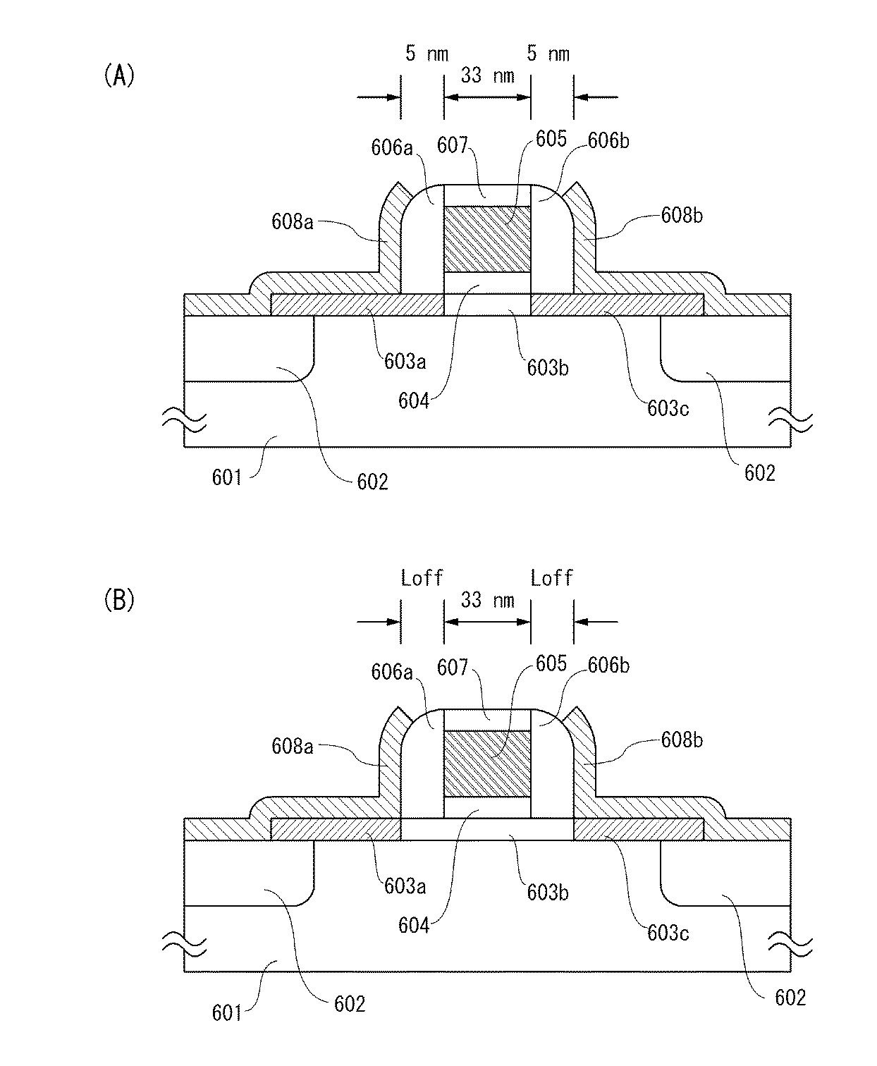
数値計算に用いたトランジスタの断面構造を図6に示す。図6に示すトランジスタは酸化物半導体層にN型の半導体領域603aおよび半導体領域603cを有する。半導体領域603aおよび半導体領域603cの抵抗率は2×10⁻³Ωcmとする。
FIG. 6 shows a cross-sectional structure of the transistor used for the numerical calculation. The transistor illustrated in FIG. 6 includes an N-
図6(A)に示すトランジスタは、下地絶縁物601と、下地絶縁物601に埋め込まれるように形成された酸化アルミニウムよりなる埋め込み絶縁物602の上に形成される。トランジスタは半導体領域603a、半導体領域603cと、それらに挟まれ、チャネル形成領域となる真性の半導体領域603bと、ゲート605を有する。ゲート605の幅を33nmとする。
The transistor illustrated in FIG. 6A is formed over a
ゲート605と半導体領域603bの間には、ゲート絶縁物604を有し、また、ゲート605の両側面には側壁絶縁物606aおよび側壁絶縁物606b、ゲート605の上部には、ゲート605と他の配線との短絡を防止するための絶縁物607を有する。側壁絶縁物の幅は5nmとする。また、半導体領域603aおよび半導体領域603cに接して、ソース608aおよびドレイン608bを有する。なお、このトランジスタにおけるチャネル幅は40nmとする。
A
数値計算では、ゲート605、ソース608a、ドレイン608bの仕事関数をそれぞれ、5.5電子ボルト、4.6電子ボルト、4.6電子ボルトとした。また、ゲート絶縁物604の厚さは100nm、比誘電率は4.1とした。チャネル長およびチャネル幅は33nmおよび40nmである。
In the numerical calculation, the work functions of the
図6(B)に示すトランジスタは、下地絶縁物601と、酸化アルミニウムよりなる埋め込み絶縁物602の上に形成され、半導体領域603a、半導体領域603cと、それらに挟まれた真性の半導体領域603bと、幅33nmのゲート605とゲート絶縁物604と側壁絶縁物606aおよび側壁絶縁物606bと絶縁物607とソース608aおよびドレイン608bを有する点で図6(A)に示すトランジスタと同じである。
The transistor illustrated in FIG. 6B is formed over a
図6(A)に示すトランジスタと図6(B)に示すトランジスタの相違点は、側壁絶縁物606aおよび側壁絶縁物606bの下の半導体領域の導電型である。図6(A)に示すトランジスタでは、側壁絶縁物606aおよび側壁絶縁物606bの下の半導体領域はN型の半導体領域603aおよび半導体領域603cであるが、図6(B)に示すトランジスタでは、真性の半導体領域603bである。
A difference between the transistor illustrated in FIG. 6A and the transistor illustrated in FIG. 6B is the conductivity type of the semiconductor region under the
すなわち、半導体領域603a(半導体領域603c)とゲート605がLoffだけ重ならない領域(オフセット領域)ができている。Loffをオフセット長という。図から明らかなように、オフセット長は、側壁絶縁物606a(側壁絶縁物606b)の幅と同じである。なお、図6(A)のトランジスタはLoffが0nmであり、オフセットトランジスタでもオーバーラップトランジスタでもない。本明細書では、このようなトランジスタをアラインドトランジスタと呼ぶことにする。
That is, a region (offset region) where the
現実には全くオーバーラップではなく、オフセットでもない構造は有りえず、若干のオーバーラップやオフセットであることは避けられないが、オーバーラップとオフセットの間の構造を持つトランジスタとして、アラインドトランジスタを用いてもよい。 In reality, there is no structure that is not an overlap at all and is not an offset, and a slight overlap or offset is inevitable, but an aligned transistor is used as a transistor having a structure between overlap and offset. It may be used.
図7において、点線は図6(A)の構造のトランジスタ(アラインドトランジスタ、Loff=0nm)の特性を示し、実線はLoffが15nmである図6(B)の構造のトランジスタ(オフセットトランジスタ)の特性を示す。 In FIG. 7, the dotted line indicates the characteristics of the transistor having the structure of FIG. 6A (aligned transistor, Loff = 0 nm), and the solid line indicates the transistor having the structure of FIG. 6B in which Loff is 15 nm (offset transistor). Show properties.
酸化物半導体はバンドギャップが2.5電子ボルト以上であるため、熱励起のキャリアが少なく、オフ状態では極めて高い抵抗を実現できる。しかしながら、シリコン半導体のように短チャネル効果を抑制するためにチャネルにドーピングをおこなうことができないので、ゲート電圧0Vでのドレイン電流は1pA以上である。 Since the oxide semiconductor has a band gap of 2.5 eV or more, the number of thermally excited carriers is small, and an extremely high resistance can be realized in an off state. However, since the channel cannot be doped in order to suppress the short channel effect unlike a silicon semiconductor, the drain current at a gate voltage of 0 V is 1 pA or more.
オフ電流は、オフセットトランジスタ(図6(B))ではより小さくなる。図6(A)のトランジスタとの比較では、ゲート電圧0Vではドレイン電流は3桁小さく、ゲート電圧が−1Vでは6桁以上小さくなる。しかしながら、オフセットトランジスタでは、オン電流はオフセットでないトランジスタよりも少なくなる。ゲート電圧+1Vでは、図6(B)のトランジスタのドレイン電流は、図6(A)のトランジスタの1/3程度である。 The off-state current is smaller in the offset transistor (FIG. 6B). In comparison with the transistor in FIG. 6A, when the gate voltage is 0V, the drain current is 3 orders of magnitude smaller, and when the gate voltage is -1V, it is 6 orders of magnitude or more. However, the on-state current is lower in the offset transistor than in the non-offset transistor. When the gate voltage is +1 V, the drain current of the transistor in FIG. 6B is about 1/3 that of the transistor in FIG.
本発明の一態様の構成により、オフセットトランジスタとそうでないトランジスタ(アラインドトランジスタ、オーバーラップトランジスタ等)を同じ基板上に同時に形成することができる。すなわち、回路内においては、オン電流が大きい方が好ましい部分にはオフセットでないトランジスタを用い、また、オフ電流が小さい方が好ましい部分にはオフセットトランジスタを用いることができる。 With the structure of one embodiment of the present invention, an offset transistor and a non-offset transistor (aligned transistor, overlap transistor, or the like) can be formed over the same substrate at the same time. That is, in the circuit, a non-offset transistor can be used for a portion where a larger on-current is preferable, and an offset transistor can be used for a portion where a smaller off-current is preferable.
以下、実施の形態について図面を参照しながら説明する。但し、実施の形態は多くの異なる態様で実施することが可能であり、趣旨及びその範囲から逸脱することなくその形態及び詳細を様々に変更し得ることは当業者であれば容易に理解される。従って、本発明は、以下の実施の形態の記載内容に限定して解釈されるものではない。 Hereinafter, embodiments will be described with reference to the drawings. However, the embodiments can be implemented in many different modes, and it is easily understood by those skilled in the art that the modes and details can be variously changed without departing from the spirit and scope thereof. . Therefore, the present invention should not be construed as being limited to the description of the following embodiments.
また、図において、大きさ、層の厚さ、又は領域は、明瞭化のために誇張されている場合がある。よって、必ずしもそのスケールに限定されない。 In the drawings, the size, the layer thickness, or the region is exaggerated for simplicity in some cases. Therefore, it is not necessarily limited to the scale.
なお、図は、理想的な例を模式的に示したものであり、図に示す形状又は値などに限定されない。例えば、製造技術による形状のばらつき、誤差による形状のばらつき、などを含むことが可能である。 The figure schematically shows an ideal example, and is not limited to the shape or value shown in the figure. For example, it is possible to include variation in shape due to manufacturing technology, variation in shape due to error, and the like.
さらに、専門用語は、特定の実施の形態、又は実施例などを述べる目的で用いられる場合が多い。ただし、発明の一態様は、専門用語によって、限定して解釈されるものではない。 Furthermore, technical terms are often used for the purpose of describing specific embodiments or examples. Note that one embodiment of the present invention is not construed as being limited by technical terms.
また、定義されていない文言(専門用語又は学術用語などの科学技術文言を含む)は、通常の当業者が理解する一般的な意味と同等の意味として用いることが可能である。辞書等により定義されている文言は、関連技術の背景と矛盾がないような意味に解釈されることが好ましい。 In addition, undefined words (including scientific and technical words such as technical terms or academic terms) can be used as meanings equivalent to general meanings understood by those skilled in the art. Words defined by a dictionary or the like are preferably interpreted in a meaning that is consistent with the background of related technology.
なお、ある一つの実施の形態の中で述べる内容(一部の内容でもよい)は、その実施の形態で述べる別の内容(一部の内容でもよい)、及び/又は、一つ若しくは複数の別の実施の形態で述べる内容(一部の内容でもよい)に対して、適用、組み合わせ、又は置き換えなどをおこなうことが出来る。 Note that the content (may be a part of content) described in one embodiment is different from the content (may be a part of content) described in the embodiment and / or one or more Application, combination, replacement, or the like can be performed on the content described in another embodiment (or part of the content).
(実施の形態1)
図1(A)に本実施の形態の半導体装置の断面図を示す。半導体装置は基板101上に第1酸化物半導体層102aと第2酸化物半導体層102bを有する。さらに、第1酸化物半導体層102aに接して、第1層配線103a、第2酸化物半導体層102bに接して、第1層配線103b、第1酸化物半導体層102aと第2酸化物半導体層102bに接して、第1層配線103cを有する。
(Embodiment 1)
FIG. 1A is a cross-sectional view of the semiconductor device of this embodiment. The semiconductor device includes a first oxide semiconductor layer 102 a and a second
そして、第1酸化物半導体層102aと第2酸化物半導体層102b、第1層配線103a、第1層配線103b、第1層配線103c上にゲート絶縁物104を有し、ゲート絶縁物104上に第2層配線105a、第2層配線105b、第2層配線105c、第2層配線105dを有する。
The
この半導体装置には、2つのトランジスタと2つの容量素子が含まれている。このうち、第1トランジスタは第2層配線105bをゲートとし、第1層配線103bを第1電極とする。また、第2トランジスタは第2層配線105aをゲートとし、第1層配線103aを第2電極とする。また、第1層配線103cは、第1トランジスタの第2電極としての機能と第2トランジスタの第1電極としての機能を有する。第1トランジスタはゲートが第1電極や第2電極が重ならない、オフセットトランジスタであり、第2トランジスタはゲートが第1電極と第2電極と重なるオーバーラップトランジスタである。
This semiconductor device includes two transistors and two capacitors. Among these, the first transistor uses the
さらに、第1容量素子は、第2層配線105cをその第2電極とする。また、第2容量素子は、第2層配線105dをその第2電極とする。なお、第1層配線103aは、第2容量素子の第1電極としての機能も有する。第1層配線103cは、第1容量素子の第1電極としての機能も有する。
Further, the first capacitor element uses the
以上の2つのトランジスタと2つの容量素子によって構成される回路を図1(D)に示す。ここで、Tr1は第1トランジスタ、Tr2は第2トランジスタ、Cs1は第1容量素子、Cs2は第2容量素子である。第1トランジスタTr1のゲートと第2トランジスタTr2のゲートは同じ信号端子CLKに接続され、第1トランジスタTr1と第2トランジスタTr2は連動して動作する。例えば、第1トランジスタTr1の第1電極は入力端子INに接続し、与えられた入力信号が第2容量素子Cs2の第1電極のノードであるストレージノードSNに保存される。なお、第1トランジスタTr1のゲートと第2トランジスタTr2のゲートを分離し、それぞれに異なる信号を入力してもよい。 A circuit including the above two transistors and two capacitors is illustrated in FIG. Here, Tr 1 is a first transistor, Tr 2 is a second transistor, Cs 1 is a first capacitor element, and Cs 2 is a second capacitor element. A first transistor of Tr 1 gate gate of the second transistor Tr 2 is connected to the same signal terminal CLK, the first transistor Tr 1 and the second transistor Tr 2 is operated in conjunction with each other. For example, the first electrode of the first transistor Tr 1 is connected to the input terminal IN, and the given input signal is stored in the storage node SN that is the node of the first electrode of the second capacitor element Cs 2 . Note that the first transistor Tr 1 gate the second transistor gate of Tr 2 are separated, may enter a different signal to each.
また、第1容量素子Cs1、第2容量素子Cs2は、意図的に形成される容量である以外に、配線間容量や寄生容量のような意図的に形成されない容量であってもよい。 Further, the first capacitor element Cs 1 and the second capacitor element Cs 2 may be capacitors that are not intentionally formed, such as inter-wiring capacitors and parasitic capacitors, in addition to the capacitors that are intentionally formed.
図1(B)に変形例を示す。図1(B)に示す半導体装置は、第2トランジスタがオフセットトランジスタであることを除けば、図1(A)の半導体装置と同じである。 A modification is shown in FIG. The semiconductor device illustrated in FIG. 1B is the same as the semiconductor device in FIG. 1A except that the second transistor is an offset transistor.
図1(C)に変形例を示す。図1(C)に示す半導体装置は、図1(A)の半導体装置では、2つ設けられていた酸化物半導体層(第1酸化物半導体層102aと第2酸化物半導体層102b)を一つの第1酸化物半導体層102としたものである。その他の構成は図1(A)の半導体装置と同じである。
A modification is shown in FIG. In the semiconductor device illustrated in FIG. 1C, two oxide semiconductor layers (a first oxide semiconductor layer 102a and a second
(実施の形態2)
本実施の形態では、オフセットトランジスタとアラインドトランジスタを同一の酸化物半導体層上に作製する方法を図2を用いて説明する。
(Embodiment 2)
In this embodiment, a method for manufacturing an offset transistor and an aligned transistor over the same oxide semiconductor layer will be described with reference to FIGS.
<図2(A)>
基板201に酸化物半導体層202を形成する。基板201には各種基板を用いることができ、例えば、単結晶シリコンウェハー、ガラス基板、SOI(Silicon on Insulator)基板等を用いることができる。また、基板201の表面は絶縁性であることが好ましく、半導体あるいは導電性の基板を用いる場合には、表面に絶縁層(以下、第1の絶縁層、という)を設けるとよい。なお、基板201上に何らかの回路を形成し、その上に第1の絶縁層を設けてもよい。
<FIG. 2 (A)>
An oxide semiconductor layer 202 is formed over the
第1の絶縁層は酸化物であることが好ましく、過剰な酸素を含有しているとより好ましい。また、その水素濃度は十分に低いことが好ましく、水素濃度は1×1019cm−3以下であることがより好ましい。そのためには、第1の絶縁層の少なくとも表面部は、十分に水素濃度の低減された雰囲気で、スパッタリング法により形成されるとよい。なお、第1の絶縁層は誘電率が低いことが好ましいので、酸化シリコンを用いるとよい。 The first insulating layer is preferably an oxide, and more preferably contains excess oxygen. Further, the hydrogen concentration is preferably sufficiently low, and the hydrogen concentration is more preferably 1 × 10 19 cm −3 or less. For this purpose, at least the surface portion of the first insulating layer is preferably formed by a sputtering method in an atmosphere with a sufficiently reduced hydrogen concentration. Note that silicon oxide is preferably used because the first insulating layer preferably has a low dielectric constant.
第1の絶縁層は表面が十分に平坦であることが好ましく、平均面粗さが1nm以下、好ましくは0.3nm以下、より好ましくは0.1nm以下とするとよい。特に、その上に形成される酸化物半導体層202が結晶性を有する場合には、表面の平坦性が十分でないと、結晶性が不十分となることがある。また、平坦性が十分でないと、トランジスタ特性のばらつきの原因となる。平坦な表面を得るためには、第1の絶縁層の表面を化学的機械的研磨法により平坦化するとよく、その後、その表面をプラズマ処理するとなお好ましい。 The first insulating layer preferably has a sufficiently flat surface, and the average surface roughness is 1 nm or less, preferably 0.3 nm or less, and more preferably 0.1 nm or less. In particular, in the case where the oxide semiconductor layer 202 formed thereover has crystallinity, the crystallinity may be insufficient if the surface flatness is not sufficient. Moreover, if the flatness is not sufficient, it causes variations in transistor characteristics. In order to obtain a flat surface, it is preferable to flatten the surface of the first insulating layer by a chemical mechanical polishing method, and then it is more preferable to perform plasma treatment on the surface.
酸化物半導体層202は、上述の酸化物半導体のいずれかを用いて形成するとよく、その厚さはトランジスタのサイズに応じて決定される。酸化物半導体層202の厚さは、例えば、1nm以上30nm以下とすればよい。あるいは、チャネル長をLとするとき、酸化物半導体層202の厚さはその1%以上10%未満となるようにするとよい。 The oxide semiconductor layer 202 is preferably formed using any of the above oxide semiconductors, and the thickness thereof is determined in accordance with the size of the transistor. For example, the thickness of the oxide semiconductor layer 202 may be greater than or equal to 1 nm and less than or equal to 30 nm. Alternatively, when the channel length is L, the thickness of the oxide semiconductor layer 202 is preferably 1% to less than 10%.
酸化物半導体層202は、酸化物半導体の膜を必要な形状にエッチングして得られる。酸化物半導体の膜は、好ましくはスパッタリング法により、基板加熱温度を100℃以上600℃以下、好ましくは150℃以上550℃以下、さらに好ましくは200℃以上500℃以下とし、酸素ガスを有する雰囲気で成膜する。酸素ガスと希ガスの混合雰囲気とする場合は、酸素ガスの割合は30体積%以上、好ましくは50体積%以上、さらに好ましくは80体積%以上とする。 The oxide semiconductor layer 202 is obtained by etching an oxide semiconductor film into a required shape. The oxide semiconductor film is preferably formed by a sputtering method with a substrate heating temperature of 100 ° C. to 600 ° C., preferably 150 ° C. to 550 ° C., more preferably 200 ° C. to 500 ° C., and an atmosphere containing oxygen gas. Form a film. In the case of a mixed atmosphere of oxygen gas and rare gas, the proportion of oxygen gas is 30% by volume or more, preferably 50% by volume or more, and more preferably 80% by volume or more.
成膜時の基板加熱温度が高いほど、得られる酸化物半導体の膜に含まれる不純物(水素等)濃度は低くなる。また、酸化物半導体膜中の原子配列が整い、高密度化され、結晶が形成されやすくなる。酸化物半導体の膜のドナー濃度は1×1011cm−3以下であることが好ましい。 The higher the substrate heating temperature during film formation, the lower the concentration of impurities (such as hydrogen) contained in the obtained oxide semiconductor film. Further, the atomic arrangement in the oxide semiconductor film is aligned, the density is increased, and crystals are easily formed. The donor concentration of the oxide semiconductor film is preferably 1 × 10 11 cm −3 or less.
次いで、ゲート絶縁物203を成膜する。ゲート絶縁物203の厚さはトランジスタのサイズに応じて決定される。ゲート絶縁物203の厚さは、例えば、5nm以上30nm以下とすればよい。あるいは、チャネル長をLとするとき、ゲート絶縁物203の厚さはその10%未満となるようにするとよい。また、ゲート絶縁物203の厚さは、その比誘電率によっても決定され、比誘電率の大きな材料を用いれば、ゲート絶縁物203を厚くすることもできる。
Next, a
なお、酸化物半導体層202の比誘電率ε1と厚さt1とゲート絶縁物203の比誘電率ε2と厚さt2とトランジスタとのチャネル長Lとの間で、(ε2t1+ε1t2)<0.1ε2L、という関係を満たすとさらに好ましい。 Note that the dielectric constant ε 1 and the thickness t 1 of the oxide semiconductor layer 202, the relative dielectric constant ε 2 and the thickness t 2 of the gate insulator 203, and the channel length L of the transistor (ε 2 t 1 + ε 1 t 2 ) <0.1ε 2 L is more preferable.
ゲート絶縁物203は、スパッタリング法、蒸着法、PCVD法、PLD法、ALD法またはMBE法を用いることができる。また、ゲート絶縁物203には、酸化シリコン、窒化シリコン、酸化窒化シリコン、酸化アルミニウム、酸化タンタル、酸化ハフニウム、酸化ジルコニウム、酸化イットリウム等を用いればよい。本実施の形態では、スパッタリング法を用いて酸化シリコン膜を100nmの厚さで成膜する。
As the
次いで、ゲート電極としても機能する第1層配線を形成するための第1の導電膜を形成する。第1の導電膜の材料は、モリブデン、チタン、タンタル、タングステン、アルミニウム、銅、クロム、ネオジム、スカンジウム等の金属材料またはこれらを主成分とする合金材料を用いて形成することができる。 Next, a first conductive film for forming a first layer wiring that also functions as a gate electrode is formed. The material of the first conductive film can be formed using a metal material such as molybdenum, titanium, tantalum, tungsten, aluminum, copper, chromium, neodymium, or scandium, or an alloy material containing these as a main component.
また、第1の導電膜を積層構造とし、その最下層に窒素を含む金属酸化物、具体的には、窒素を含むIn−Ga−Zn系酸化物や、窒素を含むIn−Sn系酸化物や、窒素を含むIn−Ga系酸化物や、窒素を含むIn−Zn系酸化物や、窒素を含む酸化錫や、窒素を含む酸化インジウムや、金属窒化膜(InN、SnNなど)を用いてもよい。 In addition, the first conductive film has a stacked structure, and a metal oxide containing nitrogen in the lowermost layer, specifically, an In—Ga—Zn-based oxide containing nitrogen or an In—Sn-based oxide containing nitrogen Or an In—Ga-based oxide containing nitrogen, an In—Zn-based oxide containing nitrogen, a tin oxide containing nitrogen, an indium oxide containing nitrogen, or a metal nitride film (InN, SnN, or the like). Also good.
これらの材料は5電子ボルト以上、好ましくは5.5電子ボルト以上の仕事関数を有し、ゲート電極として用いた場合、トランジスタのしきい値電圧をプラスにすることができ、所謂ノーマリーオフのスイッチング素子を実現できる。 These materials have a work function of 5 eV or more, preferably 5.5 eV or more, and when used as a gate electrode, the threshold voltage of a transistor can be positive, so-called normally-off. A switching element can be realized.
さらに、第1の導電膜上に第2の絶縁層を形成する。例えば、酸化シリコン、窒化シリコン、酸化窒化シリコン、酸化アルミニウム等を形成する。第2の絶縁層の材料は、その後の異方性エッチングの工程でのエッチングストッパとなるような材料であることが好ましい。 Further, a second insulating layer is formed over the first conductive film. For example, silicon oxide, silicon nitride, silicon oxynitride, aluminum oxide, or the like is formed. The material of the second insulating layer is preferably a material that serves as an etching stopper in the subsequent anisotropic etching step.
次いで、フォトリソグラフィ工程によって第1の導電膜と第2の絶縁層を加工して、第1層配線204a、第1層配線204bとその上のエッチングストッパ205a、エッチングストッパ205bを形成する。そして、オフセットトランジスタを設ける領域(図2(A)では右側)にレジスト206を形成する。
Next, the first conductive film and the second insulating layer are processed by a photolithography process to form a
<図2(B)>
レジスト206、および、第1層配線204aとその上のエッチングストッパ205aをマスクとして、酸化物半導体層202に不純物をドーピングする。用いる不純物としては、リン、硼素、窒素等が挙げられるがこれらに限定されず、酸化物半導体に含まれる酸素と化合して、酸化物半導体の酸素欠損を増加させ、酸化物半導体中のドナー濃度を高めるものであればよい。
<FIG. 2 (B)>
The oxide semiconductor layer 202 is doped with an impurity using the resist 206 and the
このようにしてN型酸化物半導体領域207が形成される。N型酸化物半導体領域207のドナー濃度は1×1020cm−3以上であることが好ましい。この際、N型酸化物半導体領域207の境界が、第1層配線204aの両端とほぼ揃った形状に形成される。
In this way, an N-type
その後、プラズマCVD法等により、第3の絶縁層を形成し、これを異方性エッチングすることで側壁絶縁物208を形成する。この工程は公知の半導体技術(側壁形成技術)を参照できる。この際、ゲート絶縁物203は、側壁絶縁物208および第1層配線204a、第1層配線204bの下にある部分を除いて、エッチングし、N型酸化物半導体領域207を露出させる。
Thereafter, a third insulating layer is formed by plasma CVD or the like, and the
<図2(C)>
第2の導電膜を形成する。第2の導電膜の材料としては、第1の導電膜に用いることのできる材料から選択すればよい。第2の導電膜をエッチングして、第2層配線209a、第2層配線209b、第2層配線209cを得る。第2層配線209aと第2層配線209bはN型酸化物半導体領域207に接する。
<Fig. 2 (C)>
A second conductive film is formed. The material for the second conductive film may be selected from materials that can be used for the first conductive film. The second conductive film is etched to obtain a
この工程により、本実施の形態の半導体装置の主要な部分が形成される。すなわち、第1トランジスタ(オフセットトランジスタ)は、第1層配線204bをゲートとし、第2層配線209cを第1電極、第2層配線209bを第2電極とする。また、第2トランジスタ(アラインドトランジスタ)は、第1層配線204aをゲートとし、第2層配線209bを第1電極、第2層配線209aを第2電極とする。
By this process, a main part of the semiconductor device of the present embodiment is formed. That is, the first transistor (offset transistor) uses the
<図2(D)>
その後、容量用絶縁物210を形成する。容量用絶縁物210は容量素子の誘電体として用いる。そのためには、その厚さと比誘電率を適切なものとするとよい。例えば、ゲート絶縁物203の厚さやそれに用いることのできる材料を参照すればよい。また、容量用絶縁物210の一部には必要に応じてコンタクトホール等を設けてもよい。
<FIG. 2 (D)>
Thereafter, the capacitor insulator 210 is formed. The capacitor insulator 210 is used as a dielectric of a capacitor element. For that purpose, the thickness and relative dielectric constant are preferably appropriate. For example, the thickness of the
その後、第3層配線211a、第3層配線211b、第3層配線211cを形成する。第3層配線211aは第2層配線209aと、第3層配線211bは第2層配線209bと、それぞれ容量素子を形成し、第3層配線211aは第2容量素子の第2電極、第3層配線211bは第1容量素子の第2電極となる。なお、第2層配線209aは第2容量素子の第1電極、第2層配線209bは第1容量素子の第1電極である。また、第3層配線211cは、第2層配線209cと接する。
Thereafter, the
さらに保護膜や層間絶縁物を設けてもよい。このようにして、酸化物半導体層202上に、オフセットトランジスタとアラインドトランジスタを形成できる。なお、アラインドトランジスタの代わりに、オーバーラップトランジスタやオフセットトランジスタを形成してもよい。 Further, a protective film or an interlayer insulator may be provided. In this manner, an offset transistor and an aligned transistor can be formed over the oxide semiconductor layer 202. Note that an overlap transistor or an offset transistor may be formed instead of the aligned transistor.
(実施の形態3)
本実施の形態では、図1(D)に示される回路を用いる例について説明する。図3(A)は図1(D)の回路を用いた記憶素子の回路を示す。この記憶素子は第1トランジスタ301と第2トランジスタ302と第1容量素子304と第2容量素子305よりなる回路(図の点線で囲まれた部分)と読み出しトランジスタ303とを有する。図の点線で囲まれた部分は図1(D)に示す回路と同様なものである。
(Embodiment 3)
In this embodiment, an example in which the circuit illustrated in FIG. 1D is used will be described. FIG. 3A shows a circuit of a memory element using the circuit of FIG. The memory element includes a circuit (a portion surrounded by a dotted line in the drawing) including a
第1トランジスタ301はオフセットトランジスタであり、第2トランジスタ302はアラインドトランジスタ、オーバーラップトランジスタ、オフセットトランジスタのいずれかであり、いずれも実施の形態1あるいは実施の形態2で示したように、酸化物半導体層を用いて構成される。
The
データを入力する際には、第1トランジスタ301と第2トランジスタ302のゲートの信号端子CLKの電位を制御し、第1トランジスタ301と第2トランジスタ302をオンとする。そして、入力端子INをデータに応じた電位とする。その結果、第1容量素子304の第1電極と第2容量素子305の第1電極の電位(ストレージノードSNの電位)をデータに応じたものとすることができる。
When inputting data, the potentials of the signal terminals CLK of the gates of the
この回路のストレージノードSNの電位によって読み出しトランジスタ303の状態が変化する。すなわち、ストレージノードSNの電位が高ければ読み出しトランジスタ303はオンとなることがあるが、ストレージノードSNの電位が低ければ読み出しトランジスタ303はオフとなる。したがって、第1端子T1と第2端子T2の導通状態を調べることで、保持されているデータを判別できる。
The state of the
似たような構造の記憶素子はゲインセル(例えば、特許文献1参照)として知られているが、図3(A)に示す回路の記憶素子は、オフ電流の低いオフセットトランジスタである第1トランジスタ301を有することにより、通常のゲインセルよりも長期間、データを保持できる。
A memory element having a similar structure is known as a gain cell (see, for example, Patent Document 1). However, the memory element in the circuit illustrated in FIG. 3A is a
図3(B)は図1(D)の回路を用いた他の記憶素子の回路を示す。この記憶素子は第1トランジスタ317と第2トランジスタ318と第1容量素子320と第2容量素子321よりなる回路(図の点線で囲まれた部分)と読み出しトランジスタ319とを有する。図の点線で囲まれた部分は図1(D)に示す回路と同様なものである。また、点線で囲まれた部分と読み出しトランジスタ319は、図3(A)で示した回路と同様のものである。
FIG. 3B illustrates a circuit of another memory element using the circuit of FIG. This memory element includes a circuit (a portion surrounded by a dotted line in the drawing) including a
第1トランジスタ317はオフセットトランジスタであり、第2トランジスタ318はアラインドトランジスタ、オーバーラップトランジスタ、オフセットトランジスタのいずれかであり、いずれも実施の形態1あるいは実施の形態2で示したように、酸化物半導体層を用いて構成される。
The
図3(B)に示す回路は、さらに、Pチャネル型トランジスタ311とNチャネル型トランジスタ313よりなる第1のインバータと、Pチャネル型トランジスタ312とNチャネル型トランジスタ314よりなる第2のインバータと、それらに接続する第1スイッチングトランジスタ315と第2スイッチングトランジスタ316とを有する。これらはフリップフロップ回路を形成するものである。このような回路は、例えば、CPUのレジスタ等に使用される。
The circuit illustrated in FIG. 3B further includes a first inverter including a P-
データを書き込む際には、入力端子INをデータに応じた電位とし、第3端子T3を適切な高電位に、第4端子T4を適切な低電位とし、さらに第1スイッチングトランジスタ315のゲートの信号端子CLK1の電位と、第2スイッチングトランジスタ316のゲートの信号端子CLK2の電位を制御し、第1スイッチングトランジスタ315と、第2スイッチングトランジスタ316をオンとする。データは第1のインバータと第2のインバータによって形成された帰還回路に維持される。その後、第1スイッチングトランジスタ315はオフとする。
When writing data, the input terminal IN is set to a potential corresponding to the data, the third terminal T3 is set to an appropriate high potential, the fourth terminal T4 is set to an appropriate low potential, and the signal of the gate of the
記憶されているデータは出力端子OUTの電位を読み取ることで判定できる。なお、出力端子OUTの電位は、入力端子INに与えられた電位とは逆位相であることに注意する必要がある。例えば、データ”1”のときに入力端子INに与える電位を+2V、データ”0”のときに入力端子INに与える電位を0Vとするとき、入力されたデータが”1”(入力端子INの電位が+2V)であれば、出力端子OUTの電位は0Vである。 The stored data can be determined by reading the potential of the output terminal OUT. Note that the potential of the output terminal OUT is opposite in phase to the potential applied to the input terminal IN. For example, when the potential applied to the input terminal IN is +2 V when the data is “1” and the potential applied to the input terminal IN is 0 V when the data is “0”, the input data is “1” (the input terminal IN If the potential is + 2V), the potential of the output terminal OUT is 0V.
上記の定常状態は、第3端子T3と第4端子T4の電位が維持されている場合に保持されるが、第3端子T3と第4端子T4の電位差が小さくなると、データが消滅してしまう。すなわち、上記のフリップフロップ回路のみでは、データを保持するには常に相当量の電力を消費する。しかし、図に点線で示す部分にデータを退避させることで、記憶素子の消費電力を低減することができる。 The above steady state is maintained when the potentials of the third terminal T3 and the fourth terminal T4 are maintained, but when the potential difference between the third terminal T3 and the fourth terminal T4 becomes small, the data disappears. . That is, with only the flip-flop circuit described above, a considerable amount of power is always consumed to hold data. However, the power consumption of the memory element can be reduced by saving data in the portion indicated by the dotted line in the drawing.
データを退避させるには、フリップフロップ回路が定常状態を保った状態で、第1トランジスタ317と第2トランジスタ318のゲートの信号端子CLK3の電位を制御して、第1トランジスタ317と第2トランジスタ318をオンとする。その結果、ストレージノードSNの電位は保持されていたデータに応じたものとなる。上記の例では、保持されていたデータが”1”の場合には、ストレージノードSNの電位は0V、保持されていたデータが”0”の場合には、ストレージノードSNの電位は+2Vとなる。
In order to save the data, the potential of the signal terminal CLK3 of the gates of the
その後、第1トランジスタ317と第2トランジスタ318のゲートの信号端子CLK3の電位を制御して、第1トランジスタ317と第2トランジスタ318をオフとする。第1スイッチングトランジスタ315と、第2スイッチングトランジスタ316もオフとするとよい。
After that, the potential of the signal terminal CLK3 of the gates of the
ストレージノードSNの電位はオフ電流の低いオフセットトランジスタである第1トランジスタ317により長期に維持される。なお、ストレージノードSNの電位は、時間の経過によって変動して、初期の値からずれることがある。
The potential of the storage node SN is maintained for a long time by the
データを上記回路に退避させている間には、信号端子CLK3の電位を回路の他の部分の電位よりも低くしてもよい。そうすることによりストレージノードSNの電位をより長時間にわたって保持できる。その際に消費される電流は極めて限定的であり、ほとんどは、第1トランジスタ317と第2トランジスタ318のゲートリーク(ゲートとソースやドレイン間のリーク電流)であり、測定することが困難なほど微量である。
While the data is saved in the circuit, the potential of the signal terminal CLK3 may be lower than the potential of other parts of the circuit. By doing so, the potential of the storage node SN can be held for a longer time. The current consumed at that time is extremely limited. Most of the current is gate leakage (leakage current between the gate, the source, and the drain) of the
退避させたデータを元に戻すには、以下のようにおこなえばよい。まず、第2スイッチングトランジスタ316と第1トランジスタ317と第2トランジスタ318はオフのままとする。また、第1スイッチングトランジスタ315をオンとして、さらに入力端子INの電位をデータ”1”に対応するもの(上記の例では+2V)とする。第5端子T5の電位もこれにあわせて+2Vとするとよい。第3端子T3、第4端子T4は、それぞれ所定の電位とする。この結果、第1のインバータのゲートの電位は+2Vとなる。その後、第1スイッチングトランジスタ315をオフとする。
In order to restore the saved data to the original state, the following may be performed. First, the
次に第5端子の電位を0Vとする。もし、ストレージノードSNの電位が0V(あるいはそれに近い値)であれば、読み出しトランジスタ319はオフであるので、第1のインバータのゲートの電位は+2Vのままである。しかし、ストレージノードSNの電位が+2V(あるいはそれに近い値)であれば、読み出しトランジスタ319はオンであるので、第1のインバータのゲートの電位は0Vとなる。
Next, the potential of the fifth terminal is set to 0V. If the potential of the storage node SN is 0V (or a value close thereto), the
ところで、保存されていたデータが”1”であれば、ストレージノードSNの電位は0V(あるいはそれに近い値)、”0”であれば+2V(あるいはそれに近い値)であったので、保存されていたデータが”1”であれば、第1のインバータのゲートの電位は+2V、保存されていたデータが”0”であれば、第1のインバータのゲートの電位は0Vとなる。この状態は最初に入力された状態と同じである。 By the way, if the stored data is “1”, the potential of the storage node SN is 0V (or a value close to it), and if it is “0”, it is + 2V (or a value close to it). If the data is “1”, the gate potential of the first inverter is + 2V, and if the stored data is “0”, the gate potential of the first inverter is 0V. This state is the same as the first input state.
その状態で、第2スイッチングトランジスタ316をオンとすると、フリップフロップ回路は第1のインバータのゲートの電位に応じた定常状態となる。この状態はデータを退避する前と同じである。
In that state, when the
このような記憶素子を作製する場合には、シリコンウェハー上に、公知の半導体作製技術を用いて、Pチャネル型トランジスタ311とNチャネル型トランジスタ313よりなる第1のインバータと、Pチャネル型トランジスタ312とNチャネル型トランジスタ314よりなる第2のインバータと、それらに接続する第1スイッチングトランジスタ315と第2スイッチングトランジスタ316とを形成し、その回路上に、酸化物半導体を用いて、第1トランジスタ317、第2トランジスタ318を形成するとよい。
In the case of manufacturing such a memory element, a first inverter including a P-
また、読み出しトランジスタ319は、フリップフロップ回路を構成するトランジスタと同じ層に形成してもよいが、第1トランジスタ317、第2トランジスタ318と同じ層に形成すると、従来の記憶素子と同じ面積で回路を作製でき、集積度を低下させなくて済む。
In addition, the reading
なお、最小加工線幅をFとするとき、フリップフロップ回路は50F2以上の面積を要するため、第1トランジスタ317、第2トランジスタ318のチャネル長を、フリップフロップ回路を構成するトランジスタのチャネル長の5倍以上としてもよい。第1トランジスタ317、第2トランジスタ318を長チャネルとすることにより、オフ特性を向上させることができる。
Note that when the minimum processing line width is F, since the flip-flop circuit requires an area of 50 F 2 or more, the channel lengths of the
(実施の形態4)
本実施の形態では、図3(B)で示したような記憶素子を作製する際に用いることのできる方法について図4および図5を用いて説明する。なお、図4および図5に示す断面図は記憶素子の特定の断面ではない。
(Embodiment 4)
In this embodiment, a method that can be used for manufacturing a memory element as illustrated in FIG. 3B will be described with reference to FIGS. 4 and 5 are not specific cross sections of the memory element.
まず、シリコンウェハー等の基板401上に公知の半導体集積回路作製技術を用いて、N型ウェル401n、P型ウェル401p、素子分離絶縁物402、N型領域403n、P型領域403p、第1層配線404a、第1層配線404bを形成する(図4(A)参照)。第1層配線404a、第1層配線404bはトランジスタのゲートとなる。
First, using a known semiconductor integrated circuit manufacturing technique on a
さらに、第1層間絶縁物405を形成し、コンタクトホールを形成して、第1コンタクトプラグ406a、第1コンタクトプラグ406b、第1コンタクトプラグ406cを形成する(図4(B)参照)。
Further, a
さらに、第2層間絶縁物407と第2層配線408a、第2層配線408b、第2層配線408c、第2層配線408dを形成する。ここまでは公知の半導体集積回路作製技術を用いることができる。なお、第2層間絶縁物407と第2層配線408a、第2層配線408b、第2層配線408c、第2層配線408dの表面は実施の形態2で説明したように、十分に平坦化しておくことが好ましい。また、第2層間絶縁物407は実施の形態2の第1の絶縁層と同様な材料で形成するとよい。
Further, a
その後、酸化物半導体層409、ゲート絶縁物410、第3層配線411a、第3層配線411b、第3層配線411c、第3層配線411dを形成する(図4(C)参照)。これらの形成に関しては、実施の形態2を参照すればよい。
After that, the
ここで、第3層配線411bと第3層配線411dは、トランジスタのゲート配線となるべきものである。本実施の形態では、第3層配線411bと第3層配線411dと酸化物半導体層409が重なる部分では、第3層配線411bと第3層配線411dは第2層配線408a、第2層配線408b、第2層配線408c、第2層配線408dと重ならないようにする。
Here, the
すなわち、図に示すように、第2層配線408bと第3層配線411b、第2層配線408cと第3層配線411b、第2層配線408cと第3層配線411d、第2層配線408dと第3層配線411dは、適切なオフセット長を有するオフセット状態となるようにする。
That is, as shown in the figure, the second layer wiring 408b and the
レジスト412をもちいて、オフセットトランジスタを作製する部分を覆い、不純物を酸化物半導体層409に注入して、N型酸化物半導体領域413を形成する(図5(A)参照)。N型酸化物半導体領域413の端は、おおよそ第3層配線411bの端と揃っているため、アラインドトランジスタを形成できる。この工程の詳細は実施の形態2を参照できる。
A resist 412 is used to cover a portion where an offset transistor is to be manufactured, and an impurity is injected into the
さらに、第3層間絶縁物414を形成する(図5(B)参照)。以上のようにして、オフセットトランジスタである第1トランジスタ415d、アラインドトランジスタである第2トランジスタ415b、第1容量素子415c、第2容量素子415aを形成できる。
Further, a
これら第1トランジスタ415d、第2トランジスタ415b、第1容量素子415c、第2容量素子415aは、図3(A)に示される第1トランジスタ301、第2トランジスタ302、第1容量素子304、第2容量素子305や図3(B)に示される第1トランジスタ317、第2トランジスタ318、第1容量素子320、第2容量素子321として使用できる。
The
また、N型領域403n、P型領域403p、第1層配線404a、第1層配線404b等によって形成されるトランジスタは、図3(B)のPチャネル型トランジスタ311、Pチャネル型トランジスタ312、Nチャネル型トランジスタ313、Nチャネル型トランジスタ314、第1スイッチングトランジスタ315、第2スイッチングトランジスタ316として使用してもよい。このようにトランジスタを多層に形成することで回路の集積度を低下させることなく、優れた特性が得られる。
The transistors formed by the N-
(実施の形態5)
本実施の形態では、上述の実施の形態で説明した半導体装置を電子機器に適用する場合について、図8を用いて説明する。本実施の形態では、コンピュータ、電子ペーパー、テレビジョン装置(テレビ、またはテレビジョン受信機ともいう)などの電子機器に、上述の半導体装置を適用する場合について説明する。
(Embodiment 5)
In this embodiment, the case where the semiconductor device described in any of the above embodiments is applied to an electronic device will be described with reference to FIGS. In this embodiment, the case where the above-described semiconductor device is applied to an electronic device such as a computer, electronic paper, or a television device (also referred to as a television or a television receiver) is described.
図8(A)は、ノート型のパーソナルコンピュータ700であり、筐体701、筐体702、表示部703、キーボード704などによって構成されている。筐体701と筐体702の少なくとも一には、先の実施の形態に示す記憶素子を有する半導体装置を設けるとよい。そのため、長期間の記憶保持が可能で、且つ消費電力が十分に低減されたノート型のパーソナルコンピュータが実現される。
FIG. 8A illustrates a laptop
図8(B)は、電子ペーパーを実装した電子書籍710であり、筐体711と筐体712の2つの筐体で構成されている。筐体711および筐体712には、それぞれ表示部713および表示部714が設けられている。筐体711と筐体712は、軸部715により接続されており、該軸部715を軸として開閉動作をおこなうことができる。
FIG. 8B illustrates an
また、筐体711は、操作キー716、電源ボタン717、スピーカー718などを備えている。筐体711、筐体712の少なくとも一には、先の実施の形態に示す記憶素子を有する半導体装置を設けるとよい。そのため、長期間の記憶保持が可能で、且つ消費電力が十分に低減された電子書籍が実現される。
The
図8(C)は、テレビジョン装置720であり、筐体721、表示部722、スタンド723などで構成されている。筐体721には、先の実施の形態に示す記憶素子を有する半導体装置が搭載できる。そのため、長期間の記憶保持が可能で、且つ消費電力が十分に低減されたテレビジョン装置が実現される。
FIG. 8C illustrates a
以上のように、本実施の形態に示す電子機器には、先の実施の形態に係る記憶素子が搭載されている。このため、長期間のデータの保存に耐え、消費電力を低減した電子機器が実現される。もちろん、図8に示された電子機器以外においても、先の実施の形態に係る半導体装置を搭載することにより同様の効果が得られる。 As described above, the electronic device described in this embodiment includes the memory element according to any of the above embodiments. Therefore, an electronic device that can withstand long-term data storage and has reduced power consumption is realized. Needless to say, the same effect can be obtained by mounting the semiconductor device according to the above embodiment other than the electronic device shown in FIG.
101 基板
102 第1酸化物半導体層
102a 第1酸化物半導体層
102b 第2酸化物半導体層
103a 第1層配線
103b 第1層配線
103c 第1層配線
104 ゲート絶縁物
105a 第2層配線
105b 第2層配線
105c 第2層配線
105d 第2層配線
201 基板
202 酸化物半導体層
203 ゲート絶縁物
204a 第1層配線
204b 第1層配線
205a エッチングストッパ
205b エッチングストッパ
206 レジスト
207 N型酸化物半導体領域
208 側壁絶縁物
209a 第2層配線
209b 第2層配線
209c 第2層配線
210 容量用絶縁物
211a 第3層配線
211b 第3層配線
211c 第3層配線
301 第1トランジスタ
302 第2トランジスタ
303 読み出しトランジスタ
304 第1容量素子
305 第2容量素子
311 Pチャネル型トランジスタ
312 Pチャネル型トランジスタ
313 Nチャネル型トランジスタ
314 Nチャネル型トランジスタ
315 第1スイッチングトランジスタ
316 第2スイッチングトランジスタ
317 第1トランジスタ
318 第2トランジスタ
319 読み出しトランジスタ
320 第1容量素子
321 第2容量素子
401 基板
401n N型ウェル
401p P型ウェル
402 素子分離絶縁物
403n N型領域
403p P型領域
404a 第1層配線
404b 第1層配線
405 第1層間絶縁物
406a 第1コンタクトプラグ
406b 第1コンタクトプラグ
406c 第1コンタクトプラグ
407 第2層間絶縁物
408a 第2層配線
408b 第2層配線
408c 第2層配線
408d 第2層配線
409 酸化物半導体層
410 ゲート絶縁物
411a 第3層配線
411b 第3層配線
411c 第3層配線
411d 第3層配線
412 レジスト
413 N型酸化物半導体領域
414 第3層間絶縁物
415a 第2容量素子
415b 第2トランジスタ
415c 第1容量素子
415d 第1トランジスタ
601 下地絶縁物
602 埋め込み絶縁物
603a 半導体領域
603b 半導体領域
603c 半導体領域
604 ゲート絶縁物
605 ゲート
606a 側壁絶縁物
606b 側壁絶縁物
607 絶縁物
608a ソース
608b ドレイン
700 パーソナルコンピュータ
701 筐体
702 筐体
703 表示部
704 キーボード
710 電子書籍
711 筐体
712 筐体
713 表示部
714 表示部
715 軸部
716 操作キー
717 電源ボタン
718 スピーカー
720 テレビジョン装置
721 筐体
722 表示部
723 スタンド
IN 入力端子
OUT 出力端子
CLK 信号端子
CLK1 信号端子
CLK2 信号端子
CLK3 信号端子
SN ストレージノード
Tr1 第1トランジスタ
Tr2 第2トランジスタ
Cs1 第1容量素子
Cs2 第2容量素子
T1 第1端子
T2 第2端子
T3 第3端子
T4 第4端子
T5 第5端子
101 Substrate 102 First oxide semiconductor layer 102a First oxide semiconductor layer 102b Second oxide semiconductor layer 103a First layer wiring 103b First layer wiring 103c First layer wiring 104 Gate insulator 105a Second layer wiring 105b Second Layer wiring 105c Second layer wiring 105d Second layer wiring 201 Substrate 202 Oxide semiconductor layer 203 Gate insulator 204a First layer wiring 204b First layer wiring 205a Etching stopper 205b Etching stopper 206 Resist 207 N-type oxide semiconductor region 208 Side wall Insulator 209a Second layer wiring 209b Second layer wiring 209c Second layer wiring 210 Capacitor insulator 211a Third layer wiring 211b Third layer wiring 211c Third layer wiring 301 First transistor 302 Second transistor 303 Read transistor 304 Second 1 capacitive element 305 Two-capacitance element 311 P-channel transistor 312 P-channel transistor 313 N-channel transistor 314 N-channel transistor 315 First switching transistor 316 Second switching transistor 317 First transistor 318 Second transistor 319 Read transistor 320 First capacitor 321 Second capacitive element 401 Substrate 401n N-type well 401p P-type well 402 Element isolation insulator 403n N-type region 403p P-type region 404a First layer wiring 404b First layer wiring 405 First interlayer insulator 406a First contact plug 406b First 1 contact plug 406c 1st contact plug 407 2nd interlayer insulator 408a 2nd layer wiring 408b 2nd layer wiring 408c 2nd layer wiring 408d 2nd layer wiring 409 Oxide Conductor layer 410 Gate insulator 411a Third layer wiring 411b Third layer wiring 411c Third layer wiring 411d Third layer wiring 412 Resist 413 N-type oxide semiconductor region 414 Third interlayer insulator 415a Second capacitor element 415b Second transistor 415c first capacitor 415d first transistor 601 base insulator 602 buried insulator 603a semiconductor region 603b semiconductor region 603c semiconductor region 604 gate insulator 605 gate 606a sidewall insulator 606b sidewall insulator 607 insulator 608a source 608b drain 700 personal computer 701 Case 702 Case 703 Display portion 704 Keyboard 710 Electronic book 711 Case 712 Case 713 Display portion 714 Display portion 715 Shaft portion 716 Operation key 717 Power button 718 Speaker 720 Revision device 721 Case 722 Display unit 723 Stand IN Input terminal OUT Output terminal CLK Signal terminal CLK1 Signal terminal CLK2 Signal terminal CLK3 Signal terminal SN Storage node Tr 1 First transistor Tr 2 Second transistor Cs 1 First capacitor Cs 2 First 2 capacitive element T1 1st terminal T2 2nd terminal T3 3rd terminal T4 4th terminal T5 5th terminal
Claims (5)
前記第1トランジスタは、第1のゲート電極と、第1のゲート絶縁物と、前記第1のゲート絶縁物を介して前記第1のゲート電極と重なる領域を有する第1の酸化物半導体層と、前記第1の酸化物半導体層と電気的に接続された第1のソース電極及び第1のドレイン電極とを有し、
前記第2トランジスタは、第2のゲート電極と、第2のゲート絶縁物と、前記第2のゲート絶縁物を介して前記第2のゲート電極と重なる領域を有する第2の酸化物半導体層と、前記第2の酸化物半導体層と電気的に接続された第2のソース電極及び第2のドレイン電極とを有し、
前記第1のソース電極及び前記第1のドレイン電極の一方は、前記第2のソース電極及び前記第2のドレイン電極の一方と電気的に接続され、
上方から見たときに、前記第1のソース電極及び前記第1のドレイン電極は、前記第1のゲート電極から離れており、
上方から見たときに、前記第2のソース電極及び前記第2のドレイン電極は、前記第2のゲート電極から離れており、
前記第2トランジスタは、不純物領域を有し、
前記不純物領域は、前記第2のゲート電極をマスクとして前記第2の酸化物半導体層に不純物をドーピングすることにより形成されたものであり、
前記第1トランジスタは、不純物領域を有していないことを特徴とする半導体装置。 A first transistor and a second transistor;
The first transistor includes a first gate electrode, a first gate insulator, and a first oxide semiconductor layer having a region overlapping with the first gate electrode with the first gate insulator interposed therebetween And a first source electrode and a first drain electrode electrically connected to the first oxide semiconductor layer,
The second transistor includes a second gate electrode, a second gate insulator, and a second oxide semiconductor layer having a region overlapping with the second gate electrode with the second gate insulator interposed therebetween. A second source electrode and a second drain electrode electrically connected to the second oxide semiconductor layer,
One of the first source electrode and the first drain electrode is electrically connected to one of the second source electrode and the second drain electrode;
When viewed from above, the first source electrode and the first drain electrode are separated from the first gate electrode,
When viewed from above, the second source electrode and the second drain electrode are separated from the second gate electrode,
The second transistor has an impurity region ,
The impurity region state, and are not formed by doping an impurity into the second oxide semiconductor layer said second gate electrode as a mask,
The semiconductor device is characterized in that the first transistor does not have an impurity region .
前記第1トランジスタは、第1のゲート電極と、第1のゲート絶縁物と、前記第1のゲート絶縁物を介して前記第1のゲート電極と重なる領域を有する第1の酸化物半導体層と、前記第1の酸化物半導体層と電気的に接続された第1のソース電極及び第1のドレイン電極とを有し、
前記第2トランジスタは、第2のゲート電極と、第2のゲート絶縁物と、前記第2のゲート絶縁物を介して前記第2のゲート電極と重なる領域を有する第2の酸化物半導体層と、前記第2の酸化物半導体層と電気的に接続された第2のソース電極及び第2のドレイン電極とを有し、
前記第1のソース電極及び前記第1のドレイン電極の一方は、前記第2のソース電極及び前記第2のドレイン電極の一方と電気的に接続され、
前記第2のソース電極及び前記第2のドレイン電極の一方は、前記第1の容量と電気的に接続され、
前記第2のソース電極及び前記第2のドレイン電極のもう一方は、前記第2の容量と電気的に接続され、
上方から見たときに、前記第1のソース電極及び前記第1のドレイン電極は、前記第1のゲート電極から離れており、
上方から見たときに、前記第2のソース電極及び前記第2のドレイン電極は、前記第2のゲート電極から離れており、
前記第2トランジスタは、不純物領域を有し、
前記不純物領域は、前記第2のゲート電極をマスクとして前記第2の酸化物半導体層に不純物をドーピングすることにより形成されたものであり、
前記第1トランジスタは、不純物領域を有していないことを特徴とする半導体装置。 A first transistor, a second transistor, a first capacitor, and a second capacitor;
The first transistor includes a first gate electrode, a first gate insulator, and a first oxide semiconductor layer having a region overlapping with the first gate electrode with the first gate insulator interposed therebetween And a first source electrode and a first drain electrode electrically connected to the first oxide semiconductor layer,
The second transistor includes a second gate electrode, a second gate insulator, and a second oxide semiconductor layer having a region overlapping with the second gate electrode with the second gate insulator interposed therebetween. A second source electrode and a second drain electrode electrically connected to the second oxide semiconductor layer,
One of the first source electrode and the first drain electrode is electrically connected to one of the second source electrode and the second drain electrode;
One of the second source electrode and the second drain electrode is electrically connected to the first capacitor,
The other of the second source electrode and the second drain electrode is electrically connected to the second capacitor,
When viewed from above, the first source electrode and the first drain electrode are separated from the first gate electrode,
When viewed from above, the second source electrode and the second drain electrode are separated from the second gate electrode,
The second transistor has an impurity region ,
The impurity region state, and are not formed by doping an impurity into the second oxide semiconductor layer said second gate electrode as a mask,
The semiconductor device is characterized in that the first transistor does not have an impurity region .
さらに第3のゲート電極を含む第3トランジスタを有し、
前記第3のゲート電極は、前記第2のソース電極及び前記第2のドレイン電極のもう一方と電気的に接続されていることを特徴とする半導体装置。 In claim 1 or 2,
A third transistor including a third gate electrode;
The semiconductor device, wherein the third gate electrode is electrically connected to the other of the second source electrode and the second drain electrode.
前記第1のゲート電極は前記第2のゲート電極と電気的に接続されていることを特徴とする半導体装置。 In any one of Claims 1 thru | or 3,
The semiconductor device, wherein the first gate electrode is electrically connected to the second gate electrode.
前記第1の酸化物半導体層と前記第2の酸化物半導体層のそれぞれは、インジウム及び亜鉛を含むことを特徴とする半導体装置。 In any one of Claims 1 thru | or 4,
Each of the first oxide semiconductor layer and the second oxide semiconductor layer contains indium and zinc.
Priority Applications (1)
| Application Number | Priority Date | Filing Date | Title |
|---|---|---|---|
| JP2012118160A JP6053105B2 (en) | 2011-05-26 | 2012-05-24 | Semiconductor device |
Applications Claiming Priority (3)
| Application Number | Priority Date | Filing Date | Title |
|---|---|---|---|
| JP2011117516 | 2011-05-26 | ||
| JP2011117516 | 2011-05-26 | ||
| JP2012118160A JP6053105B2 (en) | 2011-05-26 | 2012-05-24 | Semiconductor device |
Publications (3)
| Publication Number | Publication Date |
|---|---|
| JP2013008959A JP2013008959A (en) | 2013-01-10 |
| JP2013008959A5 JP2013008959A5 (en) | 2015-06-25 |
| JP6053105B2 true JP6053105B2 (en) | 2016-12-27 |
Family
ID=47218632
Family Applications (1)
| Application Number | Title | Priority Date | Filing Date |
|---|---|---|---|
| JP2012118160A Expired - Fee Related JP6053105B2 (en) | 2011-05-26 | 2012-05-24 | Semiconductor device |
Country Status (2)
| Country | Link |
|---|---|
| US (1) | US9171840B2 (en) |
| JP (1) | JP6053105B2 (en) |
Families Citing this family (7)
| Publication number | Priority date | Publication date | Assignee | Title |
|---|---|---|---|---|
| KR101537458B1 (en) * | 2011-04-08 | 2015-07-16 | 샤프 가부시키가이샤 | Semiconductor device and display device |
| JP5960000B2 (en) * | 2012-09-05 | 2016-08-02 | ルネサスエレクトロニクス株式会社 | Semiconductor device and manufacturing method of semiconductor device |
| KR102389073B1 (en) * | 2012-11-30 | 2022-04-22 | 가부시키가이샤 한도오따이 에네루기 켄큐쇼 | Semiconductor device |
| TWI607510B (en) * | 2012-12-28 | 2017-12-01 | 半導體能源研究所股份有限公司 | Semiconductor device and method of manufacturing semiconductor device |
| JP6111458B2 (en) * | 2013-03-28 | 2017-04-12 | 株式会社Joled | Semiconductor device, display device and electronic apparatus |
| US10002971B2 (en) * | 2014-07-03 | 2018-06-19 | Semiconductor Energy Laboratory Co., Ltd. | Semiconductor device and display device including the semiconductor device |
| JP2017027972A (en) * | 2015-07-15 | 2017-02-02 | シャープ株式会社 | Solid-state image pickup device and electronic information apparatus |
Family Cites Families (121)
| Publication number | Priority date | Publication date | Assignee | Title |
|---|---|---|---|---|
| EP0071244B1 (en) * | 1981-07-27 | 1988-11-23 | Kabushiki Kaisha Toshiba | Thin-film transistor and method of manufacture therefor |
| JPS60198861A (en) | 1984-03-23 | 1985-10-08 | Fujitsu Ltd | Thin film transistor |
| US4668968A (en) * | 1984-05-14 | 1987-05-26 | Energy Conversion Devices, Inc. | Integrated circuit compatible thin film field effect transistor and method of making same |
| JPH0244256B2 (en) | 1987-01-28 | 1990-10-03 | Kagaku Gijutsucho Mukizaishitsu Kenkyushocho | INGAZN2O5DESHIMESARERUROTSUHOSHOKEINOSOJOKOZOOJUSURUKAGOBUTSUOYOBISONOSEIZOHO |
| JPH0244258B2 (en) | 1987-02-24 | 1990-10-03 | Kagaku Gijutsucho Mukizaishitsu Kenkyushocho | INGAZN3O6DESHIMESARERUROTSUHOSHOKEINOSOJOKOZOOJUSURUKAGOBUTSUOYOBISONOSEIZOHO |
| JPH0244260B2 (en) | 1987-02-24 | 1990-10-03 | Kagaku Gijutsucho Mukizaishitsu Kenkyushocho | INGAZN5O8DESHIMESARERUROTSUHOSHOKEINOSOJOKOZOOJUSURUKAGOBUTSUOYOBISONOSEIZOHO |
| JPS63210023A (en) | 1987-02-24 | 1988-08-31 | Natl Inst For Res In Inorg Mater | Compound having a hexagonal layered structure represented by InGaZn↓4O↓7 and its manufacturing method |
| JPH0244262B2 (en) | 1987-02-27 | 1990-10-03 | Kagaku Gijutsucho Mukizaishitsu Kenkyushocho | INGAZN6O9DESHIMESARERUROTSUHOSHOKEINOSOJOKOZOOJUSURUKAGOBUTSUOYOBISONOSEIZOHO |
| JPH0244263B2 (en) | 1987-04-22 | 1990-10-03 | Kagaku Gijutsucho Mukizaishitsu Kenkyushocho | INGAZN7O10DESHIMESARERUROTSUHOSHOKEINOSOJOKOZOOJUSURUKAGOBUTSUOYOBISONOSEIZOHO |
| US5200634A (en) * | 1988-09-30 | 1993-04-06 | Hitachi, Ltd. | Thin film phototransistor and photosensor array using the same |
| JPH03108766A (en) * | 1989-09-22 | 1991-05-08 | Nippondenso Co Ltd | High breakdown strength transistor |
| JPH05251705A (en) | 1992-03-04 | 1993-09-28 | Fuji Xerox Co Ltd | Thin-film transistor |
| JP3479375B2 (en) | 1995-03-27 | 2003-12-15 | 科学技術振興事業団 | Metal oxide semiconductor device in which a pn junction is formed with a thin film transistor made of a metal oxide semiconductor such as cuprous oxide, and methods for manufacturing the same |
| DE69635107D1 (en) | 1995-08-03 | 2005-09-29 | Koninkl Philips Electronics Nv | SEMICONDUCTOR ARRANGEMENT WITH A TRANSPARENT CIRCUIT ELEMENT |
| US5612235A (en) * | 1995-11-01 | 1997-03-18 | Industrial Technology Research Institute | Method of making thin film transistor with light-absorbing layer |
| JP3625598B2 (en) | 1995-12-30 | 2005-03-02 | 三星電子株式会社 | Manufacturing method of liquid crystal display device |
| JPH10228248A (en) * | 1996-12-09 | 1998-08-25 | Semiconductor Energy Lab Co Ltd | Active matrix display device and manufacturing method thereof |
| JP4170454B2 (en) | 1998-07-24 | 2008-10-22 | Hoya株式会社 | Article having transparent conductive oxide thin film and method for producing the same |
| JP2000150861A (en) | 1998-11-16 | 2000-05-30 | Tdk Corp | Oxide thin film |
| JP3276930B2 (en) | 1998-11-17 | 2002-04-22 | 科学技術振興事業団 | Transistor and semiconductor device |
| JP4850326B2 (en) * | 1999-03-26 | 2012-01-11 | 株式会社半導体エネルギー研究所 | Method for manufacturing semiconductor device |
| JP4531194B2 (en) * | 1999-04-15 | 2010-08-25 | 株式会社半導体エネルギー研究所 | Electro-optical device and electronic apparatus |
| TW460731B (en) | 1999-09-03 | 2001-10-21 | Ind Tech Res Inst | Electrode structure and production method of wide viewing angle LCD |
| JP4089858B2 (en) | 2000-09-01 | 2008-05-28 | 国立大学法人東北大学 | Semiconductor device |
| KR20020038482A (en) | 2000-11-15 | 2002-05-23 | 모리시타 요이찌 | Thin film transistor array, method for producing the same, and display panel using the same |
| JP3997731B2 (en) | 2001-03-19 | 2007-10-24 | 富士ゼロックス株式会社 | Method for forming a crystalline semiconductor thin film on a substrate |
| JP2002289859A (en) | 2001-03-23 | 2002-10-04 | Minolta Co Ltd | Thin film transistor |
| JP4090716B2 (en) | 2001-09-10 | 2008-05-28 | 雅司 川崎 | Thin film transistor and matrix display device |
| JP3925839B2 (en) | 2001-09-10 | 2007-06-06 | シャープ株式会社 | Semiconductor memory device and test method thereof |
| WO2003040441A1 (en) | 2001-11-05 | 2003-05-15 | Japan Science And Technology Agency | Natural superlattice homologous single crystal thin film, method for preparation thereof, and device using said single crystal thin film |
| JP4164562B2 (en) | 2002-09-11 | 2008-10-15 | 独立行政法人科学技術振興機構 | Transparent thin film field effect transistor using homologous thin film as active layer |
| JP4083486B2 (en) | 2002-02-21 | 2008-04-30 | 独立行政法人科学技術振興機構 | Method for producing LnCuO (S, Se, Te) single crystal thin film |
| CN1445821A (en) | 2002-03-15 | 2003-10-01 | 三洋电机株式会社 | Forming method of ZnO film and ZnO semiconductor layer, semiconductor element and manufacturing method thereof |
| JP3933591B2 (en) | 2002-03-26 | 2007-06-20 | 淳二 城戸 | Organic electroluminescent device |
| US7339187B2 (en) | 2002-05-21 | 2008-03-04 | State Of Oregon Acting By And Through The Oregon State Board Of Higher Education On Behalf Of Oregon State University | Transistor structures |
| JP2004022625A (en) | 2002-06-13 | 2004-01-22 | Murata Mfg Co Ltd | Semiconductor device and method of manufacturing the semiconductor device |
| US7105868B2 (en) | 2002-06-24 | 2006-09-12 | Cermet, Inc. | High-electron mobility transistor with zinc oxide |
| US7067843B2 (en) | 2002-10-11 | 2006-06-27 | E. I. Du Pont De Nemours And Company | Transparent oxide semiconductor thin film transistors |
| JP4166105B2 (en) | 2003-03-06 | 2008-10-15 | シャープ株式会社 | Semiconductor device and manufacturing method thereof |
| JP2004273732A (en) | 2003-03-07 | 2004-09-30 | Sharp Corp | Active matrix substrate and manufacturing method thereof |
| JP4108633B2 (en) | 2003-06-20 | 2008-06-25 | シャープ株式会社 | THIN FILM TRANSISTOR, MANUFACTURING METHOD THEREOF, AND ELECTRONIC DEVICE |
| US7262463B2 (en) | 2003-07-25 | 2007-08-28 | Hewlett-Packard Development Company, L.P. | Transistor including a deposited channel region having a doped portion |
| US7297977B2 (en) | 2004-03-12 | 2007-11-20 | Hewlett-Packard Development Company, L.P. | Semiconductor device |
| US7145174B2 (en) | 2004-03-12 | 2006-12-05 | Hewlett-Packard Development Company, Lp. | Semiconductor device |
| CN102867855B (en) | 2004-03-12 | 2015-07-15 | 独立行政法人科学技术振兴机构 | Amorphous oxide and thin film transistor |
| US7282782B2 (en) | 2004-03-12 | 2007-10-16 | Hewlett-Packard Development Company, L.P. | Combined binary oxide semiconductor device |
| US7211825B2 (en) | 2004-06-14 | 2007-05-01 | Yi-Chi Shih | Indium oxide-based thin film transistors and circuits |
| JP2006100760A (en) | 2004-09-02 | 2006-04-13 | Casio Comput Co Ltd | Thin film transistor and manufacturing method thereof |
| US7285501B2 (en) | 2004-09-17 | 2007-10-23 | Hewlett-Packard Development Company, L.P. | Method of forming a solution processed device |
| US7298084B2 (en) | 2004-11-02 | 2007-11-20 | 3M Innovative Properties Company | Methods and displays utilizing integrated zinc oxide row and column drivers in conjunction with organic light emitting diodes |
| US7453065B2 (en) | 2004-11-10 | 2008-11-18 | Canon Kabushiki Kaisha | Sensor and image pickup device |
| CA2585190A1 (en) | 2004-11-10 | 2006-05-18 | Canon Kabushiki Kaisha | Amorphous oxide and field effect transistor |
| CN101057333B (en) | 2004-11-10 | 2011-11-16 | 佳能株式会社 | Light emitting device |
| RU2358355C2 (en) | 2004-11-10 | 2009-06-10 | Кэнон Кабусики Кайся | Field transistor |
| US7829444B2 (en) | 2004-11-10 | 2010-11-09 | Canon Kabushiki Kaisha | Field effect transistor manufacturing method |
| US7863611B2 (en) | 2004-11-10 | 2011-01-04 | Canon Kabushiki Kaisha | Integrated circuits utilizing amorphous oxides |
| US7791072B2 (en) | 2004-11-10 | 2010-09-07 | Canon Kabushiki Kaisha | Display |
| US7579224B2 (en) | 2005-01-21 | 2009-08-25 | Semiconductor Energy Laboratory Co., Ltd. | Method for manufacturing a thin film semiconductor device |
| TWI569441B (en) | 2005-01-28 | 2017-02-01 | 半導體能源研究所股份有限公司 | Semiconductor device, electronic device, and method of manufacturing semiconductor device |
| TWI505473B (en) | 2005-01-28 | 2015-10-21 | 半導體能源研究所股份有限公司 | Semiconductor device, electronic device, and method of manufacturing semiconductor device |
| US7858451B2 (en) | 2005-02-03 | 2010-12-28 | Semiconductor Energy Laboratory Co., Ltd. | Electronic device, semiconductor device and manufacturing method thereof |
| US7948171B2 (en) | 2005-02-18 | 2011-05-24 | Semiconductor Energy Laboratory Co., Ltd. | Light emitting device |
| US20060197092A1 (en) | 2005-03-03 | 2006-09-07 | Randy Hoffman | System and method for forming conductive material on a substrate |
| US8681077B2 (en) | 2005-03-18 | 2014-03-25 | Semiconductor Energy Laboratory Co., Ltd. | Semiconductor device, and display device, driving method and electronic apparatus thereof |
| WO2006105077A2 (en) | 2005-03-28 | 2006-10-05 | Massachusetts Institute Of Technology | Low voltage thin film transistor with high-k dielectric material |
| US7645478B2 (en) | 2005-03-31 | 2010-01-12 | 3M Innovative Properties Company | Methods of making displays |
| JP4849817B2 (en) | 2005-04-08 | 2012-01-11 | ルネサスエレクトロニクス株式会社 | Semiconductor memory device |
| US8300031B2 (en) | 2005-04-20 | 2012-10-30 | Semiconductor Energy Laboratory Co., Ltd. | Semiconductor device comprising transistor having gate and drain connected through a current-voltage conversion element |
| JP2006344849A (en) | 2005-06-10 | 2006-12-21 | Casio Comput Co Ltd | Thin film transistor |
| US7691666B2 (en) | 2005-06-16 | 2010-04-06 | Eastman Kodak Company | Methods of making thin film transistors comprising zinc-oxide-based semiconductor materials and transistors made thereby |
| US7402506B2 (en) | 2005-06-16 | 2008-07-22 | Eastman Kodak Company | Methods of making thin film transistors comprising zinc-oxide-based semiconductor materials and transistors made thereby |
| US7507618B2 (en) | 2005-06-27 | 2009-03-24 | 3M Innovative Properties Company | Method for making electronic devices using metal oxide nanoparticles |
| KR100711890B1 (en) | 2005-07-28 | 2007-04-25 | 삼성에스디아이 주식회사 | OLED display and manufacturing method thereof |
| JP2007059128A (en) | 2005-08-23 | 2007-03-08 | Canon Inc | Organic EL display device and manufacturing method thereof |
| JP5116225B2 (en) | 2005-09-06 | 2013-01-09 | キヤノン株式会社 | Manufacturing method of oxide semiconductor device |
| JP2007073705A (en) | 2005-09-06 | 2007-03-22 | Canon Inc | Oxide semiconductor channel thin film transistor and method for manufacturing the same |
| JP4850457B2 (en) | 2005-09-06 | 2012-01-11 | キヤノン株式会社 | Thin film transistor and thin film diode |
| JP4280736B2 (en) | 2005-09-06 | 2009-06-17 | キヤノン株式会社 | Semiconductor element |
| EP1998373A3 (en) | 2005-09-29 | 2012-10-31 | Semiconductor Energy Laboratory Co, Ltd. | Semiconductor device having oxide semiconductor layer and manufacturing method thereof |
| JP5037808B2 (en) | 2005-10-20 | 2012-10-03 | キヤノン株式会社 | Field effect transistor using amorphous oxide, and display device using the transistor |
| KR20090130089A (en) | 2005-11-15 | 2009-12-17 | 가부시키가이샤 한도오따이 에네루기 켄큐쇼 | Diodes and Active Matrix Displays |
| TWI292281B (en) | 2005-12-29 | 2008-01-01 | Ind Tech Res Inst | Pixel structure of active organic light emitting diode and method of fabricating the same |
| KR101186292B1 (en) * | 2006-01-10 | 2012-09-27 | 삼성전자주식회사 | Transistor and fabrication method thereof and organic light emitting display adopting the transistor |
| US7867636B2 (en) | 2006-01-11 | 2011-01-11 | Murata Manufacturing Co., Ltd. | Transparent conductive film and method for manufacturing the same |
| JP4977478B2 (en) | 2006-01-21 | 2012-07-18 | 三星電子株式会社 | ZnO film and method of manufacturing TFT using the same |
| US7576394B2 (en) | 2006-02-02 | 2009-08-18 | Kochi Industrial Promotion Center | Thin film transistor including low resistance conductive thin films and manufacturing method thereof |
| US7977169B2 (en) | 2006-02-15 | 2011-07-12 | Kochi Industrial Promotion Center | Semiconductor device including active layer made of zinc oxide with controlled orientations and manufacturing method thereof |
| KR20070101595A (en) | 2006-04-11 | 2007-10-17 | 삼성전자주식회사 | ZnO TFT |
| JP5285235B2 (en) * | 2006-04-28 | 2013-09-11 | 株式会社半導体エネルギー研究所 | Semiconductor device |
| US20070252928A1 (en) | 2006-04-28 | 2007-11-01 | Toppan Printing Co., Ltd. | Structure, transmission type liquid crystal display, reflection type display and manufacturing method thereof |
| JP5028033B2 (en) | 2006-06-13 | 2012-09-19 | キヤノン株式会社 | Oxide semiconductor film dry etching method |
| JP4609797B2 (en) | 2006-08-09 | 2011-01-12 | Nec液晶テクノロジー株式会社 | Thin film device and manufacturing method thereof |
| JP4999400B2 (en) | 2006-08-09 | 2012-08-15 | キヤノン株式会社 | Oxide semiconductor film dry etching method |
| JP4332545B2 (en) | 2006-09-15 | 2009-09-16 | キヤノン株式会社 | Field effect transistor and manufacturing method thereof |
| JP4274219B2 (en) | 2006-09-27 | 2009-06-03 | セイコーエプソン株式会社 | Electronic devices, organic electroluminescence devices, organic thin film semiconductor devices |
| JP5164357B2 (en) | 2006-09-27 | 2013-03-21 | キヤノン株式会社 | Semiconductor device and manufacturing method of semiconductor device |
| US7622371B2 (en) | 2006-10-10 | 2009-11-24 | Hewlett-Packard Development Company, L.P. | Fused nanocrystal thin film semiconductor and method |
| US7772021B2 (en) | 2006-11-29 | 2010-08-10 | Samsung Electronics Co., Ltd. | Flat panel displays comprising a thin-film transistor having a semiconductive oxide in its channel and methods of fabricating the same for use in flat panel displays |
| JP2008140684A (en) | 2006-12-04 | 2008-06-19 | Toppan Printing Co Ltd | Color EL display and manufacturing method thereof |
| KR101303578B1 (en) | 2007-01-05 | 2013-09-09 | 삼성전자주식회사 | Etching method of thin film |
| US8207063B2 (en) | 2007-01-26 | 2012-06-26 | Eastman Kodak Company | Process for atomic layer deposition |
| KR100851215B1 (en) | 2007-03-14 | 2008-08-07 | 삼성에스디아이 주식회사 | Thin film transistor and organic light emitting display device using same |
| US7795613B2 (en) | 2007-04-17 | 2010-09-14 | Toppan Printing Co., Ltd. | Structure with transistor |
| KR101325053B1 (en) | 2007-04-18 | 2013-11-05 | 삼성디스플레이 주식회사 | Thin film transistor substrate and manufacturing method thereof |
| KR20080094300A (en) | 2007-04-19 | 2008-10-23 | 삼성전자주식회사 | Thin film transistors and methods of manufacturing the same and flat panel displays comprising thin film transistors |
| KR101334181B1 (en) | 2007-04-20 | 2013-11-28 | 삼성전자주식회사 | Thin Film Transistor having selectively crystallized channel layer and method of manufacturing the same |
| WO2008133345A1 (en) | 2007-04-25 | 2008-11-06 | Canon Kabushiki Kaisha | Oxynitride semiconductor |
| KR101345376B1 (en) | 2007-05-29 | 2013-12-24 | 삼성전자주식회사 | Fabrication method of ZnO family Thin film transistor |
| JP5215158B2 (en) | 2007-12-17 | 2013-06-19 | 富士フイルム株式会社 | Inorganic crystalline alignment film, method for manufacturing the same, and semiconductor device |
| TWI413260B (en) | 2008-07-31 | 2013-10-21 | 半導體能源研究所股份有限公司 | Semiconductor device and method of manufacturing same |
| JP5372435B2 (en) * | 2008-09-02 | 2013-12-18 | 株式会社ジャパンディスプレイ | Display device |
| JP4623179B2 (en) | 2008-09-18 | 2011-02-02 | ソニー株式会社 | Thin film transistor and manufacturing method thereof |
| KR101623958B1 (en) * | 2008-10-01 | 2016-05-25 | 삼성전자주식회사 | Inverter, method of operating the same and logic circuit comprising inverter |
| JP5451280B2 (en) | 2008-10-09 | 2014-03-26 | キヤノン株式会社 | Wurtzite crystal growth substrate, manufacturing method thereof, and semiconductor device |
| EP2184783B1 (en) * | 2008-11-07 | 2012-10-03 | Semiconductor Energy Laboratory Co, Ltd. | Semiconductor device and method for manufacturing the same |
| TWI549198B (en) * | 2008-12-26 | 2016-09-11 | 半導體能源研究所股份有限公司 | Semiconductor device and method of manufacturing same |
| EP2284891B1 (en) * | 2009-08-07 | 2019-07-24 | Semiconductor Energy Laboratory Co, Ltd. | Semiconductor device and manufacturing method thereof |
| WO2011027664A1 (en) | 2009-09-04 | 2011-03-10 | Semiconductor Energy Laboratory Co., Ltd. | Liquid crystal display device and method for manufacturing the same |
| KR20240042253A (en) * | 2009-10-29 | 2024-04-01 | 가부시키가이샤 한도오따이 에네루기 켄큐쇼 | Semiconductor device |
| KR101932909B1 (en) | 2010-03-04 | 2018-12-27 | 가부시키가이샤 한도오따이 에네루기 켄큐쇼 | Semiconductor memory device and semiconductor device |
| WO2011142371A1 (en) | 2010-05-14 | 2011-11-17 | Semiconductor Energy Laboratory Co., Ltd. | Semiconductor device |
-
2012
- 2012-05-23 US US13/478,675 patent/US9171840B2/en not_active Expired - Fee Related
- 2012-05-24 JP JP2012118160A patent/JP6053105B2/en not_active Expired - Fee Related
Also Published As
| Publication number | Publication date |
|---|---|
| US9171840B2 (en) | 2015-10-27 |
| US20120298987A1 (en) | 2012-11-29 |
| JP2013008959A (en) | 2013-01-10 |
Similar Documents
| Publication | Publication Date | Title |
|---|---|---|
| US12057451B2 (en) | Logic circuit, processing unit, electronic component, and electronic device | |
| JP6053105B2 (en) | Semiconductor device | |
| US11404585B2 (en) | Semiconductor device and method for manufacturing semiconductor device | |
| CN102436846B (en) | Storage devices and semiconductor devices | |
| US8929161B2 (en) | Signal processing circuit | |
| KR102384624B1 (en) | semiconductor device | |
| JP6648987B2 (en) | Semiconductor devices and electronic equipment | |
| TWI613762B (en) | Semiconductor device | |
| KR20120130063A (en) | Semiconductor device | |
| US9438234B2 (en) | Logic circuit and semiconductor device including logic circuit | |
| US9424890B2 (en) | Semiconductor device and driving method thereof | |
| JP5815466B2 (en) | Semiconductor device | |
| KR20120120066A (en) | Memory element and memory device | |
| US9812466B2 (en) | Semiconductor device | |
| JP2012256855A (en) | Semiconductor element, memory circuit, integrated circuit, and driving method for integrated circuit | |
| JP6076616B2 (en) | Semiconductor device | |
| KR20120130062A (en) | Semiconductor device | |
| JP5936908B2 (en) | Parity bit output circuit and parity check circuit |
Legal Events
| Date | Code | Title | Description |
|---|---|---|---|
| A521 | Request for written amendment filed |
Free format text: JAPANESE INTERMEDIATE CODE: A523 Effective date: 20150508 |
|
| A621 | Written request for application examination |
Free format text: JAPANESE INTERMEDIATE CODE: A621 Effective date: 20150508 |
|
| A131 | Notification of reasons for refusal |
Free format text: JAPANESE INTERMEDIATE CODE: A131 Effective date: 20160517 |
|
| A977 | Report on retrieval |
Free format text: JAPANESE INTERMEDIATE CODE: A971007 Effective date: 20160519 |
|
| A521 | Request for written amendment filed |
Free format text: JAPANESE INTERMEDIATE CODE: A523 Effective date: 20160624 |
|
| TRDD | Decision of grant or rejection written | ||
| A01 | Written decision to grant a patent or to grant a registration (utility model) |
Free format text: JAPANESE INTERMEDIATE CODE: A01 Effective date: 20161122 |
|
| A61 | First payment of annual fees (during grant procedure) |
Free format text: JAPANESE INTERMEDIATE CODE: A61 Effective date: 20161128 |
|
| R150 | Certificate of patent or registration of utility model |
Ref document number: 6053105 Country of ref document: JP Free format text: JAPANESE INTERMEDIATE CODE: R150 |
|
| R250 | Receipt of annual fees |
Free format text: JAPANESE INTERMEDIATE CODE: R250 |
|
| LAPS | Cancellation because of no payment of annual fees |