JP5955519B2 - Nitride semiconductor device and manufacturing method thereof - Google Patents
Nitride semiconductor device and manufacturing method thereof Download PDFInfo
- Publication number
- JP5955519B2 JP5955519B2 JP2011192411A JP2011192411A JP5955519B2 JP 5955519 B2 JP5955519 B2 JP 5955519B2 JP 2011192411 A JP2011192411 A JP 2011192411A JP 2011192411 A JP2011192411 A JP 2011192411A JP 5955519 B2 JP5955519 B2 JP 5955519B2
- Authority
- JP
- Japan
- Prior art keywords
- nitride semiconductor
- layer
- nitride
- electrode
- source electrode
- Prior art date
- Legal status (The legal status is an assumption and is not a legal conclusion. Google has not performed a legal analysis and makes no representation as to the accuracy of the status listed.)
- Expired - Fee Related
Links
Images


Classifications
-
- H10P10/00—
-
- H—ELECTRICITY
- H10—SEMICONDUCTOR DEVICES; ELECTRIC SOLID-STATE DEVICES NOT OTHERWISE PROVIDED FOR
- H10D—INORGANIC ELECTRIC SEMICONDUCTOR DEVICES
- H10D30/00—Field-effect transistors [FET]
- H10D30/01—Manufacture or treatment
- H10D30/015—Manufacture or treatment of FETs having heterojunction interface channels or heterojunction gate electrodes, e.g. HEMT
-
- H—ELECTRICITY
- H10—SEMICONDUCTOR DEVICES; ELECTRIC SOLID-STATE DEVICES NOT OTHERWISE PROVIDED FOR
- H10D—INORGANIC ELECTRIC SEMICONDUCTOR DEVICES
- H10D30/00—Field-effect transistors [FET]
- H10D30/40—FETs having zero-dimensional [0D], one-dimensional [1D] or two-dimensional [2D] charge carrier gas channels
- H10D30/47—FETs having zero-dimensional [0D], one-dimensional [1D] or two-dimensional [2D] charge carrier gas channels having 2D charge carrier gas channels, e.g. nanoribbon FETs or high electron mobility transistors [HEMT]
- H10D30/471—High electron mobility transistors [HEMT] or high hole mobility transistors [HHMT]
- H10D30/475—High electron mobility transistors [HEMT] or high hole mobility transistors [HHMT] having wider bandgap layer formed on top of lower bandgap active layer, e.g. undoped barrier HEMTs such as i-AlGaN/GaN HEMTs
- H10D30/4755—High electron mobility transistors [HEMT] or high hole mobility transistors [HHMT] having wider bandgap layer formed on top of lower bandgap active layer, e.g. undoped barrier HEMTs such as i-AlGaN/GaN HEMTs having wide bandgap charge-carrier supplying layers, e.g. modulation doped HEMTs such as n-AlGaAs/GaAs HEMTs
-
- H—ELECTRICITY
- H10—SEMICONDUCTOR DEVICES; ELECTRIC SOLID-STATE DEVICES NOT OTHERWISE PROVIDED FOR
- H10D—INORGANIC ELECTRIC SEMICONDUCTOR DEVICES
- H10D64/00—Electrodes of devices having potential barriers
- H10D64/111—Field plates
- H10D64/112—Field plates comprising multiple field plate segments
-
- H—ELECTRICITY
- H10—SEMICONDUCTOR DEVICES; ELECTRIC SOLID-STATE DEVICES NOT OTHERWISE PROVIDED FOR
- H10D—INORGANIC ELECTRIC SEMICONDUCTOR DEVICES
- H10D64/00—Electrodes of devices having potential barriers
- H10D64/20—Electrodes characterised by their shapes, relative sizes or dispositions
- H10D64/27—Electrodes not carrying the current to be rectified, amplified, oscillated or switched, e.g. gates
- H10D64/311—Gate electrodes for field-effect devices
- H10D64/411—Gate electrodes for field-effect devices for FETs
-
- H—ELECTRICITY
- H10—SEMICONDUCTOR DEVICES; ELECTRIC SOLID-STATE DEVICES NOT OTHERWISE PROVIDED FOR
- H10D—INORGANIC ELECTRIC SEMICONDUCTOR DEVICES
- H10D62/00—Semiconductor bodies, or regions thereof, of devices having potential barriers
- H10D62/80—Semiconductor bodies, or regions thereof, of devices having potential barriers characterised by the materials
- H10D62/85—Semiconductor bodies, or regions thereof, of devices having potential barriers characterised by the materials being Group III-V materials, e.g. GaAs
- H10D62/8503—Nitride Group III-V materials, e.g. AlN or GaN
Landscapes
- Junction Field-Effect Transistors (AREA)
- Electrodes Of Semiconductors (AREA)
- Thin Film Transistor (AREA)
- Insulated Gate Type Field-Effect Transistor (AREA)
Description
本発明は、窒化物半導体素子及びその製造方法に関し、詳しくは、ノーマリ−オフ(Normally−off)動作する窒化物半導体素子及びその製造方法に関する。 The present invention relates to a nitride semiconductor device and a manufacturing method thereof, and more particularly to a nitride semiconductor device that operates normally-off and a manufacturing method thereof.
グリーンエネルギ政策などによる電力消費の節減への関心が増加している。このため、電力変換効率の向上は必須な要素となる。電力変換において、パワースイッチング素子の効率が全体電力変換の効率を左右する。 There is an increasing interest in reducing power consumption through green energy policies. For this reason, improvement in power conversion efficiency is an essential element. In power conversion, the efficiency of the power switching element determines the efficiency of overall power conversion.
現在、通常利用される電力素子は、シリコンを用いるパワーMOSFETやIGBTが大部分であるが、シリコンの材料的な限界によって素子の効率向上に限界が生ずるようになる。これを解決するために、窒化ガリウム(Gallium nitride:GaN)のような窒化物半導体を用いるトランジスタを製作して、変換効率を高めるような特許が出願されている。 Currently, power MOSFETs and IGBTs that use silicon are the most commonly used power devices. However, there is a limit in improving the efficiency of the device due to the material limitations of silicon. In order to solve this problem, a patent has been filed in which a transistor using a nitride semiconductor such as gallium nitride (GaN) is manufactured to increase the conversion efficiency.
しかし、GaNを用いる、例えば、高電子移動度トランジスタ(HEMT)構造は、ゲート電圧が0V(ノーマル状態)の時、ドレイン電極とソース電極との間の抵抗が低くて電流が流れるようになるオン状態になる。これによって、電流及び電力の消耗が発生し、これをオフ状態にするためには、ゲート電極に陰電圧(例えば、−5V)を加えなければならないという短所がある(ノーマリ−オン(Normally−on)構造)。 However, for example, a high electron mobility transistor (HEMT) structure using GaN has a low resistance between the drain electrode and the source electrode when the gate voltage is 0 V (normal state), and the current flows. It becomes a state. As a result, current and power are consumed, and a negative voltage (for example, −5 V) must be applied to the gate electrode in order to turn it off (normally-on). )Construction).
このようなノーマリ−オン構造の短所を解決するために、図6及び図7のような特許出願が従来に示されている。図6及び図7は、従来の高電子移動度HEMT構造を示す。 In order to solve the disadvantages of the normally-on structure, patent applications as shown in FIGS. 6 and 7 are conventionally shown. 6 and 7 show a conventional high electron mobility HEMT structure.
図6は、米国特許出願公開第2007/0295993号の図面を示す。 図6では、AlGaN層でゲート(G)の下部領域と、ゲート(G)とドレイン(D)との間のゲート電極(G)に近い領域にイオンを打ち込み、AlGaN層133成長で形成されたチャネルの濃度を調節している。図6では、イオンインプラ(ion implantation)を用いて、ゲート(G)下部のチャネル領域131のキャリア濃度を調節してノーマリ−オフ(Normally−off)動作を具現した。
図7は、米国特許第7038253号の図面であって、第1及び第2の電子共与層133a、133b間に形成されたチャネル層131上を絶縁層140で塗布し、絶縁層140上にゲート電極(G)を形成し、ゲート電極(G)の下部で2DEGチャネル135が形成されないようにしている。図7では、ゲート(G)下部をリセス(recess)工程を用いてエッチングし、ノーマルオフ動作を具現した。
FIG. 6 shows a drawing of US Patent Application Publication No. 2007/0295993. In FIG. 6, ions are implanted into the lower region of the gate (G) and the region near the gate electrode (G) between the gate (G) and the drain (D) in the AlGaN layer, and formed by the growth of the
FIG. 7 is a drawing of US Pat. No. 7,038,253, in which a
前述のようなノーマリ−オン構造の問題を解決すると共にノーマリ−オフ動作する半導体素子を具現する必要がある。 It is necessary to realize a semiconductor device that solves the above-described problem of the normally-on structure and operates normally-off.
本発明は上記の問題点に鑑みて成されたものであって、その目的は、半導体素子、例えばFETのソース領域にショットキー(Schottky)電極を形成し、内部にオミックパターン電極を備え、ゲート電極をソース電極の一部領域と窒化物半導体領域の一部に形成することによって、ノーマリ−オフ(Normally−off;N−off)またはエンハンスメントモード(Enhancement Mode)動作すると共に高耐圧及び高電流で動作可能な、半導体素子及び製造方法を提供することにある。 The present invention has been made in view of the above problems, and its purpose is to form a Schottky electrode in the source region of a semiconductor element, for example, an FET, and to provide an ohmic pattern electrode inside, By forming the gate electrode in a part of the source electrode and a part of the nitride semiconductor region, a normally-off (N-off) or enhancement mode (enhancement mode) operation is performed, and a high breakdown voltage and a high current are achieved. It is an object to provide a semiconductor device and a manufacturing method that can be operated in a semiconductor device.
上記目的を解決するために、本発明の好適な実施形態によれば、基板上部に配設され、内部に2次元電子ガス(2DEG)チャネルを形成する窒化物半導体層と、該窒化物半導体層にオミック接合されたドレイン電極と、該ドレイン電極と離間配設され、該窒化物半導体層にショットキー接合され、内部に該窒化物半導体層にオミック接合されるオミックパターンを含むソース電極と、該ドレイン電極と該ソース電極との間の窒化物半導体層上及び該ソース電極の少なくとも一部上にかけて形成された誘電層と、該ドレイン電極と離間して誘電層上に配設され、一部が誘電層を挟んでソース電極のドレイン方向のエッジ部分上部に形成されたゲート電極と、を含む窒化物半導体素子が提供される。 In order to solve the above-described object, according to a preferred embodiment of the present invention, a nitride semiconductor layer disposed on a substrate and forming a two-dimensional electron gas (2DEG) channel therein, and the nitride semiconductor layer A drain electrode that is ohmically bonded to the drain electrode, a source electrode including an ohm pattern that is spaced apart from the drain electrode, Schottky-bonded to the nitride semiconductor layer, and ohmically bonded to the nitride semiconductor layer inside, A dielectric layer formed on the nitride semiconductor layer between the drain electrode and the source electrode and on at least a portion of the source electrode; and disposed on the dielectric layer spaced apart from the drain electrode; And a gate electrode formed on the edge portion in the drain direction of the source electrode with a dielectric layer interposed therebetween.
本発明の実施形態によれば、ソース電極のドレイン方向のエッジ部分上部に形成されたゲート電極の一部は、ソース電極のオミックパターンの少なくとも一部をカバーするように形成される。 According to the embodiment of the present invention, a part of the gate electrode formed on the edge part in the drain direction of the source electrode is formed to cover at least a part of the ohmic pattern of the source electrode.
本発明の実施形態によれば、オミックパターンは、格子配列構造を有する。 According to the embodiment of the present invention, the ohmic pattern has a lattice arrangement structure.
本発明の実施形態によれば、オミックパターンは、ドレイン電極の配列と平行にまたは垂直方向に配設された多数の棒構造を有する。 According to an embodiment of the present invention, the ohmic pattern has a number of bar structures arranged in parallel or perpendicular to the array of drain electrodes.
本発明の実施形態によれば、窒化物半導体層は、基板上に配設され、窒化ガリウム系列材料を含む第1の窒化物層と、該第1の窒化物層上に異種接合され、第1の窒化物層より広いエネルギバンドギャップを有する異種の窒化ガリウム系列材料を含む第2の窒化物層と、を含む。 According to an embodiment of the present invention, the nitride semiconductor layer is disposed on the substrate, and the first nitride layer including the gallium nitride series material is heterogeneously bonded to the first nitride layer. A second nitride layer comprising a dissimilar gallium nitride series material having a wider energy band gap than the one nitride layer.
望ましくは、第1の窒化物層は、窒化ガリウム(GaN)を含み、第2の窒化物層は、アルミニウム窒化ガリウム(AlGaN)、インジウム窒化ガリウム(InGaN)及びインジウムアルミニウム窒化ガリウム(InAlGaN)のうちのいずれか一つを含む。 Preferably, the first nitride layer includes gallium nitride (GaN), and the second nitride layer includes aluminum gallium nitride (AlGaN), indium gallium nitride (InGaN), and indium aluminum gallium nitride (InAlGaN). Including any one of
また、上記目的を解決するために、本発明の他の好適な実施形態によれば、基板上に配設され、内部に2次元電子ガス(2DEG)チャネルを形成する窒化物半導体層と、該窒化物半導体層にオミック接合されたドレイン電極と、該ドレイン電極と離間配設され、窒化物半導体層にショットキー接合され、内部に窒化物半導体層にオミック接合されるオミックパターンを含むソース電極と、ドレイン電極とソース電極との間の窒化物半導体層上及び該ソース電極の少なくとも一部上にかけて形成された誘電層と、該誘電層を挟んでソース電極のドレイン方向のエッジ部分上部に形成された第1の領域、及びドレイン電極とソース電極との間の誘電層上にドレイン電極と離間して配設された第2の領域を含むゲート電極と、を含む窒化物半導体素子が提供される。 In order to solve the above object, according to another preferred embodiment of the present invention, a nitride semiconductor layer disposed on a substrate and forming a two-dimensional electron gas (2DEG) channel therein, A drain electrode that is ohmically joined to the nitride semiconductor layer, and a source electrode that is spaced apart from the drain electrode, is schottky joined to the nitride semiconductor layer, and is ohmically joined to the nitride semiconductor layer inside A dielectric layer formed on the nitride semiconductor layer between the drain electrode and the source electrode and on at least a part of the source electrode, and on the edge portion in the drain direction of the source electrode with the dielectric layer interposed therebetween And a gate electrode including a second region spaced apart from the drain electrode on the dielectric layer between the drain electrode and the source electrode. The child is provided.
本発明の実施形態によれば、ゲート電極は、第1の領域及び第2の領域に分離され、該第2の領域は、フローティングゲートを形成する。 According to an embodiment of the present invention, the gate electrode is separated into a first region and a second region, and the second region forms a floating gate.
本発明の実施形態によれば、第1の領域は、ソース電極のオミックパターンの少なくとも一部をカバーするように形成される。 According to the embodiment of the present invention, the first region is formed to cover at least a part of the ohmic pattern of the source electrode.
本発明の実施形態によれば、オミックパターンは、格子配列構造を有する。 According to the embodiment of the present invention, the ohmic pattern has a lattice arrangement structure.
本発明の実施形態によれば、オミックパターンは、ドレイン電極の配列と平行にまたは垂直方向に配設された多数の棒構造を有する。 According to an embodiment of the present invention, the ohmic pattern has a number of bar structures arranged in parallel or perpendicular to the array of drain electrodes.
本発明の実施形態によれば、窒化物半導体層は、基板上に配設され、窒化ガリウム系列材料を含む第1の窒化物層と、該第1の窒化物層上に異種接合され、該第1の窒化物層より広いエネルギバンドギャップを有する異種の窒化ガリウム系列材料を含む第2の窒化物層と、を含む。望ましくは、第1の窒化物層は、窒化ガリウム(GaN)を含み、第2の窒化物層は、アルミニウム窒化ガリウム(AlGaN)、インジウム窒化ガリウム(InGaN)及びインジウムアルミニウム窒化ガリウム(InAlGaN)のうちのいずれか一つを含む。 According to an embodiment of the present invention, the nitride semiconductor layer is disposed on the substrate, and is heterogeneously bonded to the first nitride layer including the gallium nitride series material, the first nitride layer, A second nitride layer comprising a dissimilar gallium nitride series material having a wider energy band gap than the first nitride layer. Preferably, the first nitride layer includes gallium nitride (GaN), and the second nitride layer includes aluminum gallium nitride (AlGaN), indium gallium nitride (InGaN), and indium aluminum gallium nitride (InAlGaN). Including any one of
本発明によれば、窒化物半導体素子は、基板と窒化物半導体層との間にバッファ層をさらに含む。 According to the present invention, the nitride semiconductor device further includes a buffer layer between the substrate and the nitride semiconductor layer.
本発明によれば、基板は、シリコン(Si)、シリコンカーバイド(SiC)及びサファイヤ(Al2O3)のうちの少なくともいずれか一つを用いる基板である。 According to the present invention, the substrate is a substrate using at least one of silicon (Si), silicon carbide (SiC), and sapphire (Al 2 O 3 ).
本発明によれば、誘電層は、SiN、SiO2及びAl2O3のうちの少なくともいずれか一つを含む。 According to the present invention, the dielectric layer comprises SiN, the at least one of SiO 2 and Al 2 O 3.
本発明によれば、窒化物半導体素子は、パワートランジスタ素子である。 According to the present invention, the nitride semiconductor device is a power transistor device.
また、上記目的を解決するために、本発明のさらに他の好適な実施形態によれば、基板上部に、内部に2次元電子ガス(2DEG)チャネルを生成する窒化物半導体層を形成するステップと、該窒化物半導体層にオミック接合されるドレイン電極と、該ドレイン電極と離間配設され、該窒化物半導体層にショットキー接合され、内部に窒化物半導体層にオミック接合されるオミックパターンを含むソース電極を形成するステップと、ドレイン電極とソース電極との間の窒化物半導体層上及び該ソース電極の少なくとも一部上にかけて誘電層を形成するステップと、ドレイン電極と離間して誘電層上にゲート電極を形成し、ゲート電極の一部をソース電極のドレイン方向のエッジ部分上部の誘電層上に形成するステップと、を含む窒化物半導体素子の製造方法が提供される。 In order to solve the above object, according to still another preferred embodiment of the present invention, a nitride semiconductor layer that generates a two-dimensional electron gas (2DEG) channel is formed in an upper portion of a substrate. A drain electrode that is ohmically joined to the nitride semiconductor layer, an ohmic pattern that is spaced apart from the drain electrode, is Schottky joined to the nitride semiconductor layer, and is ohmically joined to the nitride semiconductor layer Forming a source electrode including, forming a dielectric layer on the nitride semiconductor layer between the drain electrode and the source electrode and over at least a portion of the source electrode, and on the dielectric layer spaced from the drain electrode Forming a gate electrode on the dielectric layer, and forming a part of the gate electrode on the dielectric layer above the edge portion in the drain direction of the source electrode. Method of manufacturing a child is provided.
本発明によれば、前記ゲート電極を形成するステップにおいて、ソース電極のドレイン方向のエッジ部分上部に形成されたゲート電極の一部がソース電極のオミックパターンの少なくとも一部をカバーするようにゲート電極を形成する。 According to the present invention, in the step of forming the gate electrode, the gate is formed such that a part of the gate electrode formed on the edge part in the drain direction of the source electrode covers at least a part of the ohmic pattern of the source electrode. An electrode is formed.
本発明によれば、前記ソース電極を形成するステップにおいて、オミックパターンは、格子配列構造を有する。また、一実施形態によれば、前記ソース電極を形成するステップにおいて、オミックパターンは、ドレイン電極の配列と平行にまたは垂直方向に配設された多数の棒構造を有する。 According to the present invention, in the step of forming the source electrode, the ohmic pattern has a lattice arrangement structure. According to one embodiment, in the step of forming the source electrode, the ohmic pattern has a number of bar structures arranged in parallel or perpendicular to the arrangement of the drain electrodes.
本発明によれば、前記窒化物半導体層を形成するステップは、基板上部に窒化ガリウム系列材料を含む第1の窒化物層をエピタキシャル成長させて形成するステップと、該第1の窒化物層をシード層として該第1の窒化物層より広いエネルギバンドギャップを有する異種の窒化ガリウム系列材料を含む第2の窒化物層をエピタキシャル成長させて形成するステップと、を含む。 According to the present invention, the step of forming the nitride semiconductor layer includes the step of epitaxially growing a first nitride layer containing a gallium nitride series material on the substrate, and seeding the first nitride layer. And epitaxially growing a second nitride layer containing a dissimilar gallium nitride series material having an energy band gap wider than that of the first nitride layer as a layer.
また、上記目的を解決するために、本発明のさらに他の好適な実施形態によれば、基板上に、内部に2次元電子ガス(2DEG)チャネルを生成する窒化物半導体層を形成するステップと、該窒化物半導体層にオミック接合されるドレイン電極と、該ドレイン電極と離間配設され、該窒化物半導体層にショットキー接合され、内部に窒化物半導体層にオミック接合されるオミックパターンを含むソース電極を形成するステップと、ドレイン電極とソース電極との間の窒化物半導体層上及び該ソース電極の少なくとも一部上にかけて誘電層を形成するステップと、誘電層を挟んでソース電極のドレイン方向のエッジ部分上部に形成された第1の領域、及びドレイン電極とソース電極との間の誘電層上にドレイン電極と離間して配設された第2の領域を含むゲート電極を形成するステップと、を含む窒化物半導体素子の製造方法が提供される。 In order to solve the above object, according to still another preferred embodiment of the present invention, a nitride semiconductor layer that generates a two-dimensional electron gas (2DEG) channel is formed on a substrate. A drain electrode that is ohmically joined to the nitride semiconductor layer, an ohmic pattern that is spaced apart from the drain electrode, is Schottky joined to the nitride semiconductor layer, and is ohmically joined to the nitride semiconductor layer Forming a source electrode including: a step of forming a dielectric layer on the nitride semiconductor layer between the drain electrode and the source electrode and on at least a part of the source electrode; and a drain of the source electrode across the dielectric layer A first region formed on the edge portion in the direction, and a second region spaced apart from the drain electrode on the dielectric layer between the drain electrode and the source electrode Forming a gate electrode including a frequency, method of manufacturing a nitride semiconductor device comprising is provided.
本発明によれば、前記ゲート電極を形成するステップにおいて、第1の領域及び第2の領域を分離して前記ゲート電極を形成し、前記第2の領域は、ドレイン電極とソース電極との間の誘電層上にフローティングゲートとして形成される。 According to the present invention, in the step of forming the gate electrode, the first region and the second region are separated to form the gate electrode, and the second region is between the drain electrode and the source electrode. Formed as a floating gate on the dielectric layer.
本発明によれば、前記ゲート電極を形成するステップにおいて、第1の領域がソース電極のオミックパターンの少なくとも一部をカバーするように前記ゲート電極を形成する。 According to the present invention, in the step of forming the gate electrode, the gate electrode is formed so that the first region covers at least a part of the ohmic pattern of the source electrode.
また、本発明による窒化物半導体素子の製造方法は、前記窒化物半導体層を形成するステップにおいて、基板上部に窒化物半導体層を形成する前に、該基板上にバッファ層を形成するステップを、さらに含む。 Further, in the method of manufacturing a nitride semiconductor device according to the present invention, in the step of forming the nitride semiconductor layer, before forming the nitride semiconductor layer on the substrate, forming a buffer layer on the substrate, In addition.
本発明によれば、半導体素子、例えばFETのソース領域にショットキー電極を形成し、内部にオミックパターン電極を備え、ゲート電極をソース電極の一部領域と窒化物半導体領域の一部に形成することによって、ノーマリ−オフまたはエンハンスメントモード動作すると共に高耐圧及び高電流で動作可能な半導体素子を得ることができる。 According to the present invention, a Schottky electrode is formed in a source region of a semiconductor element, for example, an FET, an ohmic pattern electrode is provided therein, and a gate electrode is formed in a part of the source electrode and a part of the nitride semiconductor region. By doing so, it is possible to obtain a semiconductor element that operates in a normally-off or enhancement mode and that can operate at a high breakdown voltage and a high current.
また、本発明によれば、既存のGaNノーマリ−オフ素子に比べて高耐圧及び高電流で動作可能であると共に、製造工程が簡単で素子の製作が容易となる。すなわち、従来のノーマリ−オフHEMTのイオン注入、200〜300オングストロング厚さのAlGaN層のエッチングなどの高難易度の工程が必要ではなく、その製作が容易となる。 Further, according to the present invention, it is possible to operate at a higher breakdown voltage and a higher current than the existing GaN normally-off device, and the manufacturing process is simple and the device can be easily manufactured. That is, high-difficult steps such as conventional ion implantation of normally-off HEMT and etching of an AlGaN layer having a thickness of 200 to 300 angstroms are not necessary, and the fabrication is facilitated.
また、本発明によれば、ソース電極のショットキー障壁によってリーク電流を防止する構造によって、既存ノーマリ−オフHEMTに比べてリーク電流が低く耐圧が高くなるという効果が奏し、ショットキーソース電極内にオミックパターン電極を備えてオン抵抗を低くして高電流動作が可能になるという効果が奏する。 In addition, according to the present invention, the structure in which the leakage current is prevented by the Schottky barrier of the source electrode has the effect that the leakage current is lower and the withstand voltage is higher than that of the existing normally-off HEMT. There is an effect that an ohmic pattern electrode is provided and the on-resistance is lowered to enable high current operation.
また、本発明によれば、ゲート構造がソース電極のエッジ部分上部及びドレイン電極とソース電極との間の誘電層上に形成されており、電界が分散して耐圧を高めるフィールドプレートの役割も共に果たすと共に、ソース電極とゲート電極との間の距離が短く、トランスコンダクタンス(transconductance)が高くなるという長所がある。 In addition, according to the present invention, the gate structure is formed on the upper edge portion of the source electrode and on the dielectric layer between the drain electrode and the source electrode, and the role of the field plate that increases the breakdown voltage by dispersing the electric field is also provided. In addition, the distance between the source electrode and the gate electrode is short and the transconductance is high.
以下、本発明の好適な実施の形態は図面を参考にして詳細に説明する。次に示される各実施の形態は当業者にとって本発明の思想が十分に伝達されることができるようにするために例として挙げられるものである。従って、本発明は以下示している各実施の形態に限定されることなく他の形態で具体化されることができる。そして、図面において、装置の大きさ及び厚さなどは便宜上誇張して表現されることができる。明細書全体に渡って同一の参照符号は同一の構成要素を示している。 Hereinafter, preferred embodiments of the present invention will be described in detail with reference to the drawings. Each embodiment shown below is given as an example so that those skilled in the art can sufficiently communicate the idea of the present invention. Therefore, the present invention is not limited to the embodiments described below, but can be embodied in other forms. In the drawings, the size and thickness of the device can be exaggerated for convenience. Like reference numerals refer to like elements throughout the specification.
本明細書で使われた用語は、実施形態を説明するためのものであって、本発明を制限しようとするものではない。本明細書において、単数形は文句で特別に言及しない限り複数形も含む。明細書で使われる「含む」とは、言及された構成要素、ステップ、動作及び/又は素子は、一つ以上の他の構成要素、ステップ、動作及び/又は素子の存在または追加を排除しないことに理解されたい。 The terminology used herein is for the purpose of describing embodiments and is not intended to limit the invention. In this specification, the singular includes the plural unless specifically stated otherwise. As used herein, “includes” a stated component, step, action, and / or element does not exclude the presence or addition of one or more other components, steps, actions, and / or elements. Want to be understood.
図1は、本発明の一実施形態による窒化物半導体素子の概略的な断面図であって、図4a〜図4b中のI−I’に沿った断面図である。図2a〜図2dは各々、図1の窒化物半導体素子の製造方法を概略的に示す断面図である。図3は、本発明の他の実施形態による窒化物半導体素子の概略的な断面図である。図4a〜図4cは各々、本発明の実施形態による窒化物半導体素子の概略的な平面図である。図5は、本発明のさらに他の実施形態による窒化物半導体素子の概略的な断面図である。 FIG. 1 is a schematic cross-sectional view of a nitride semiconductor device according to an embodiment of the present invention, taken along line I-I ′ in FIGS. 4 a to 4 b. 2a to 2d are cross-sectional views schematically showing a method for manufacturing the nitride semiconductor device of FIG. FIG. 3 is a schematic cross-sectional view of a nitride semiconductor device according to another embodiment of the present invention. 4a to 4c are schematic plan views of a nitride semiconductor device according to an embodiment of the present invention. FIG. 5 is a schematic cross-sectional view of a nitride semiconductor device according to still another embodiment of the present invention.
まず、図1、図3、図4a〜図4c及び図5を参照して、本発明の一実施形態による窒化物半導体素子を詳記する。 First, a nitride semiconductor device according to an embodiment of the present invention will be described in detail with reference to FIGS. 1, 3, 4 a to 4 c and 5.
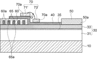
図1、図3及び図5に示すように、本発明の一実施形態による窒化物半導体素子は、基板10上に配設された窒化物半導体層30、ドレイン電極50、ソース電極60、誘電層40及びゲート電極70を含む。
As shown in FIGS. 1, 3, and 5, the nitride semiconductor device according to the embodiment of the present invention includes a
図1及び図5に示すように、本実施形態において、窒化物半導体層30は、基板10上に配設される。基板10は、一般に絶縁基板を用いて、実に絶縁性及び高抵抗性を有する基板を用いてもよい。
As shown in FIGS. 1 and 5, in the present embodiment, the
本発明の他の一実施形態によれば、図1、図3及び図5に示すように、基板10は、シリコン(Si)、シリコンカーバイド(SiC)及びサファイヤ(Al2O3)のうちの少なくともいずれか一つを用いて製造されることができ、または公知の他の基板材料を用いて製造されることができる。
According to another embodiment of the present invention, as shown in FIGS. 1, 3 and 5, the
窒化物半導体層30は、基板10上に直接形成されてもよい。望ましくは、窒化物半導体層30は、窒化物単結晶薄膜をエピタキシャル成長させて形成する。窒化物半導体層30を形成するためのエピタキシャル成長工程には、液相成長法(LPE:Liquid Phase Epitaxy)、化学気相蒸着法(CVD:Chemical Vapor Deposition)、分子ビーム成長法(MBE:Molecular Beam Epitaxy)、有機金属気相蒸着法(MOCVD:Metalorganic CVD)などが挙げられる。
The
また、図3を参照して、本発明の他の実施形態によれば、基板10と窒化物半導体層30との間にバッファ層20を設け、窒化物半導体層30をバッファ層20上に形成する。バッファ層20は、基板10と窒化物半導体層30との格子不整合(lattice mismatch)による問題点を解決するために提供される。バッファ層20は、一つの層だけではなく、窒化ガリウム(GaN)、アルミニウム窒化ガリウム(AlGaN)、窒化アルミニウム(AlN)、インジウム窒化ガリウム(InGaN)またはインジウムアルミニウム窒化ガリウム(InAlGaN)などを含む複数の層で形成されることができる。また、バッファ層20は、窒化ガリウム以外の他の3−5族化合物半導体によって形成することもできる。例えば、基板10がサファイヤ基板10の場合、窒化ガリウムを含む窒化物半導体層30との格子定数及び熱膨脹係数の差によって誤整合(mismatch)になることを阻むために、バッファ層20の成長は重要である。
Referring to FIG. 3, according to another embodiment of the present invention,
図1、図3及び図5を参照して、窒化物半導体層30の内部には、2次元電子ガス(2DEG)チャネル35が形成される。窒化物半導体素子のゲート電極70にバイアス電圧を印加すると、窒化物半導体層30内の2DEGチャネル35を通じて電子が移動し、電流がドレイン電極50とソース電極60との間に流れるようになる。窒化物半導体層30を成す窒化物としては、窒化ガリウム(GaN)、アルミニウム窒化ガリウム(AlGaN)、インジウム窒化ガリウム(InGaN)、インジウムアルミニウム窒化ガリウム(InAlGaN)などが挙げられる。
With reference to FIGS. 1, 3, and 5, a two-dimensional electron gas (2DEG)
本発明の実施形態によれば、窒化物半導体層30は、異種接合された窒化ガリウム系列の半導体層30であって、異種接合された界面でエネルギバンドギャップの差によって2次元電子ガスチャネル35が形成される。異種接合される窒化ガリウム系列の半導体層30で異種接合間の格子定数差が小さいほど、バンドギャップとの極性の差が減るようになり、これにより2DEGチャネル35の形成が抑制される。異種接合の時、エネルギバンドギャップの不連続性によって広いバンドギャップを有する材料から小さなバンドギャップを有する材料への自由電子が移動するようになる。このような電子は、異種接合界面に蓄積されて2DEGチャネル35を形成し、ドレイン電極50とソース電極60との間で電流が流れるようにする。
According to the embodiment of the present invention, the
図1、図3及び図5に示すように、窒化物半導体層30は、第1窒化物層31及び第2の窒化物層33を含む。第1窒化物層31は、基板10上に配設され、窒化ガリウム系列の材料を含む。第2の窒化物層33は、第窒化物層31上に異種接合され、該第1窒化物層31より広いエネルギバンドギャップを有する異種の窒化ガリウム系列の材料を含む。この時、第2の窒化物層33は、第1窒化物層31内に形成される2DEGチャネル35へ電子を供給する役割をする。一例として、電子を供与する第2の窒化物層33は、第1の窒化物層31より薄い厚さで形成されることが望ましい。
As shown in FIGS. 1, 3, and 5, the
望ましくは、本発明の実施形態によれば、第1の窒化物層31は、窒化ガリウム(GaN)を含み、第2の窒化物層33は、アルミニウム窒化ガリウム(AlGaN)、インジウム窒化ガリウム(InGaN)及びインジウムアルミニウム窒化ガリウム(InAlGaN)のうちのいずれか一つを含む。望ましくは、一実施形態によれば、第1の窒化物層31は、窒化ガリウム(GaN)を含み、第2の窒化物層33は、アルミニウム窒化ガリウム(AlGaN)を含む。
Preferably, according to the embodiment of the present invention, the
続いて、図1、図3、図4a〜図4c及び図5を参照して、本発明の実施形態の構成がより詳しく説明する。 Subsequently, the configuration of the embodiment of the present invention will be described in more detail with reference to FIGS. 1, 3, 4 a to 4 c and FIG. 5.
図1、図3、図4a〜図4c及び図5に示すように、本実施形態による窒化物半導体素子のドレイン電極50及びソース電極60が窒化物半導体層30に形成される。ドレイン電極50は、窒化物半導体層30にオミック接合50aされている。
As shown in FIGS. 1, 3, 4 a to 4 c and 5, the
ソース電極60は、ドレイン電極50と離間して配設され、窒化物半導体層30にショットキー接合60aされる。ショットキーソース電極60の構造によって、逆方向バイアスによって逆方向に駆動される時、ソース電極60のショットキー接合領域60aで生成される空乏領域によって2次元電子ガス(2DEG)による電流の流れを安定して遮断することができる。これによって、逆方向電流の流れを遮断することができ、ノーマリ−オフ状態を具現することができるようになる。より詳しくは、逆方向バイアス電圧が印加された場合、ソース電極60のショットキー接合領域60aで生成される空乏領域が2DEGチャネル35領域まで拡張され、2DEGチャネル35を遮断し、逆方向降伏電流を増加させるようになる。特に、逆方向バイアス電圧の印加時、ソース電極60のドレイン側のコーナー寄りのショットキー接合領域60aで空乏領域が大きく拡張される。一方、順方向バイアス電圧をかけると、ソース電極60のショットキー接合領域60aで生成される空乏領域が小さくなり、2DEGチャネル35を通じてドレイン電極50とソース電極60との間に電流が流れるようになる。
The
また、本発明では、図1、図3、図4a〜図4c及び図5に示すように、ソース電極60内部に窒化物半導体層30にオミック接合65aされるオミックパターン65を含ませてソース電極60を形成する。本発明において、ソース電極60内部の下端界面のショットキー接合パターン60a間のオミックコンタック65aされたオミックパターン電極65を通じる電流が増加するようにして、オン抵抗を低くした。オン抵抗を低くすることによって高電流動作が可能になった。ショットキー金属電極60の形成の前に、ショットキーソース電極60内部の下端領域に一定のパターンを有するオミックパターン電極65が形成されるようにし、オミックパターン電極65周囲で窒化物半導体層30とショットキー接合60aされるようにソース電極60を形成することによって、オン抵抗を低くして高電流動作が可能になる。
In the present invention, as shown in FIGS. 1, 3, 4 a to 4 c, and FIG. 5, the
図4aに示すように、本発明によれば、オミックパターン65は、格子配列構造を有する。
As shown in FIG. 4a, according to the present invention, the
図4b及び図4cに示すように、本発明によれば、オミックパターン65は、ドレイン電極50の配列と平行にまたは垂直に配設された多数の棒構造を有する。
As shown in FIGS. 4 b and 4 c, according to the present invention, the
図4a〜図4cに示すように、オミックパターン電極65をソース電極60の領域に配設させ、ショットキー接合60a間でオミック接合面65aを通じて電流が増加するようにし、順方向バイアス電圧の印加によるオン抵抗を低くして高電流動作が可能にする。
As shown in FIGS. 4a to 4c, an
続いて、図1、図3、図4a〜図4c及び図5に示すように、本発明の実施形態による窒化物半導体素子の誘電層40は、ドレイン電極50とソース電極60との間の窒化物半導体層30上及びソース電極60の少なくとも一部上にかけて形成される。
Subsequently, as shown in FIGS. 1, 3, 4 a to 4 c and FIG. 5, the
望ましくは、本発明の実施形態によれば、図1、図3、図4a〜図4c及び図5に示すように、誘電層40は、酸化膜からなることができ、また、SiN、SiO2及びAl2O3のうちの少なくともいずれか一つを含むことができる。
Desirably, according to the embodiment of the present invention, as shown in FIGS. 1, 3, 4a to 4c and 5, the
続いて、図1、図3、図4a〜図4c及び図5に示すように、本実施形態による窒化物半導体素子のゲート電極70は、ドレイン電極50と離間して誘電層40上に配設される。また、図1、図3、図4a〜図4c及び図5に示すように、ゲート電極70の一部が誘電層40を挟んでソース電極60のドレイン方向へのエッジ部分上部に形成される。望ましくは、ゲート電極70は、誘電層40上にショットキー接合70aされる。ゲート電極70に順方向バイアス電圧が印加されると、ソース電極60のドレイン側のコーナー寄りのショットキー接合領域60aで形成される空乏領域が小さくなり、2DEGチャネル35を通じてドレイン電極50とソース電極60との間に電流が流れるようになる。
Subsequently, as shown in FIGS. 1, 3, 4 a to 4 c and FIG. 5, the
図1、図3及び図4a〜図4cに示すように、ゲート構造がソース電極60のエッジ部分上部及びドレイン電極50とソース電極60との間の誘電層40上に亘っており、電界の分散する効果があり、ゲート構造自体が耐圧を高めるフィールドプレートの役割を果たすようになる。
図1、図3、図4a〜図4c及び図5に示すように、本発明の実施形態をよれば、ソース電極60のドレイン方向のエッジ部分上部に形成されたゲート電極70の一部71、71’は、ソース電極60のオミックパターン65の少なくとも一部をカバーするように形成される。
また、図1及び図5を参照して、本発明の他の実施形態について詳記する。
As shown in FIGS. 1, 3, and 4 a to 4 c, the gate structure extends over the edge portion of the
As shown in FIGS. 1, 3, 4 a to 4 c, and 5, according to the embodiment of the present invention, a
Further, another embodiment of the present invention will be described in detail with reference to FIGS. 1 and 5.
図1及び図5に示すように、本発明の一実施形態による窒化物半導体素子は、基板10上に配設された窒化物半導体層30、ドレイン電極50、ソース電極60、誘電層40及びゲート電極70を含む。窒化物半導体層30、ドレイン電極50、ソース電極60及び誘電層40については、前述のようである。
As shown in FIGS. 1 and 5, the nitride semiconductor device according to the embodiment of the present invention includes a
本実施形態において、ゲート電極70は、第1の領域71、71’及び第2の領域73、73’を備える。第1の領域71、71’は、誘電層40を挟んでソース電極60のドレイン方向へのエッジ部分上部に形成されている。第2の領域73、73’は、ドレイン電極50とソース電極60との間の誘電層40上にドレイン電極50と離間して配設される。第1の領域と第2の領域とは、図1に示すように、一体に形成されてもよく、図5に示すように分離されてもよい。
In the present embodiment, the
図1及び図5に示すように、本発明の実施形態において、第1の領域71、71’は、ソース電極60のオミックパターン65の少なくとも一部をカバーするように形成される。
As shown in FIGS. 1 and 5, in the embodiment of the present invention, the
図5に示すように、本発明の実施形態によれば、ゲート電極70の第1の領域71’及び第2の領域73’は分離されている。この時、第2の領域73’は、フローティングゲートを形成する。第2の領域73’がフローティングゲート役割を行うため、第2の領域73’によって電界の分散するという効果が奏する。望ましくは、第2の領域73’は、ソース電極60に近く配設される。
As shown in FIG. 5, according to the embodiment of the present invention, the first region 71 'and the second region 73' of the
示されていないが、本発明の実施形態によれば、第1の領域71’と第2の領域73’とに分離されたゲート電極70の構造を有する窒化物半導体素子は、図4aに示すように、格子配列構造のオミックパターン電極65を備える。また、第1の領域71’と第2領域73’とに分離されたゲート電極70の構造を有する窒化物半導体素子のオミックパターン電極65は、図4b及び図4cに示すように、ドレイン電極50の配列と平行にまたは垂直に配設された多数の棒構造を備える。オミックパターン電極65をソース電極60の領域に配設し、順方向バイアス電圧の印加によるオン抵抗を低くして高電流動作が可能なようにする。
Although not shown, according to an embodiment of the present invention, a nitride semiconductor device having a structure of a
図5には示されていないが、本発明の実施形態によれば、図3に示すように、基板10と窒化物半導体層30との間にバッファ層20を設け、窒化物半導体層30をバッファ層20上に形成する。
Although not shown in FIG. 5, according to the embodiment of the present invention, as shown in FIG. 3, the
図1、図3、図4a〜図4c及び図5に示すように、本発明の実施形態によれば、ゲート電極70に0Vの電圧印加時、ドレイン電極50とソース電極60との間に2DEGチャネル35を通じる電流の流れがソース電極60の領域のショットキー障壁によって遮られる。そして、ゲート電極70に閾値(threshold)電圧以上を駆動した時、ソース電極60のドレイン方向のエッジ領域にキャリア(電子)濃度が高くなってトンネリング(tunnellng)現象によって電流が流れるようになる。この時、ゲートの閾値電圧は、誘電層40の厚さなどによって決まる。これによって、既存のノーマリ−オフHEMT構造に比べて製作が容易で、リーク電流が少なく、高い耐圧特性を現わすようになる
As shown in FIGS. 1, 3, 4 a to 4 c, and 5, according to the embodiment of the present invention, when a voltage of 0 V is applied to the
本発明の他の実施形態によれば、前述の実施形態による窒化物半導体素子は、パワートランジスタ素子である。本発明の一実施形態によるパワートランジスタは、水平型HEMT構造を備える。 According to another embodiment of the present invention, the nitride semiconductor device according to the previous embodiment is a power transistor device. A power transistor according to an embodiment of the present invention has a horizontal HEMT structure.
次に、本発明の他の実施形態による窒化物半導体製造方法を図面を参照して説明する。本発明による窒化物半導体製造方法を説明するに当たって、図2a〜図2dの他に、前述の実施形態による窒化物半導体素子及び図1、図3、図4a〜図4c及び図5を参照する。 Next, a nitride semiconductor manufacturing method according to another embodiment of the present invention will be described with reference to the drawings. In describing the nitride semiconductor manufacturing method according to the present invention, in addition to FIGS. 2a to 2d, the nitride semiconductor device according to the above-described embodiment and FIGS. 1, 3, 4a to 4c, and 5 are referred to.
図2a〜図2dは、本発明の一実施形態による窒化物半導体の製造方法を示す。 2a to 2d illustrate a method for manufacturing a nitride semiconductor according to an embodiment of the present invention.
望ましくは、一実施形態によれば、本発明の窒化物半導体素子の製造方法によって製造される素子は、パワートランジスタである。 Preferably, according to one embodiment, the device manufactured by the method for manufacturing a nitride semiconductor device of the present invention is a power transistor.
まず、図2aを参照して、基板10上に、内部に2次元電子ガス(2DEG)チャネル35を生成する窒化物半導体層30を形成する。望ましくは、基板10は、シリコン(Si)、シリコンカーバイド(SiC)及びサファイヤ(Al2O3)のうちの少なくともいずれか一つを用いて製造されることができる。窒化物半導体層30を成す窒化物としては、窒化ガリウム(GaN)、アルミニウム窒化ガリウム(AlGaN)、インジウム窒化ガリウム(InGaN)またはインジウムアルミニウム窒化ガリウム(InAlGaN)などが挙げられる。
First, referring to FIG. 2 a, a
望ましくは、窒化物半導体層30は、窒化物単結晶薄膜をエピタキシャル成長させて形成する。望ましくは、エピタキシャル成長の時、選択的に成長させて過成長されないように調節する。仮に、過成長された場合には、エッチバック(etch back)工程やCMP(Chemical Mechanical Polishing)工程を用いて平坦化する過程を追加してもよい。
Desirably, the
本発明の他の実施形態による窒化物半導体の製造方法によれば、図2aに示された第1窒化物層31及び第2の窒化物層33は、エピタキシャル成長工程(Epitaxial Growth Precess)によって形成される。まず、第1窒化物層31は、基板10上に窒化ガリウム系列単結晶薄膜をエピタキシャル成長させて形成する。望ましくは、本発明の他の実施形態によれば、第1の窒化物層31は、窒化ガリウム(GaN)をエピタキシャル成長させて形成する。続いて、第2窒化物層33は、第1窒化物層31をシード層として第1窒化物層31より広いエネルギバンドギャップを有する異種の窒化ガリウム系列の材料を含む窒化物層をエピタキシャル成長させて形成する。望ましくは、本発明の他の実施形態によれば、第2窒化物層33は、アルミニウム窒化ガリウム(AlGaN)、インジウム窒化ガリウム(InGaN)、インジウムアルミニウム窒化ガリウム(InAlGaN)のうちのいずれか一つを含む窒化ガリウム系列単結晶をエピタキシャル成長させて形成する。望ましくは、第2窒化物層33は、アルミニウム窒化ガリウム(AlGaN)をエピタキシャル成長させて形成する。一例として、電子を供与する第2窒化物層33は、第1窒化物層31より薄い厚さで形成されることが望ましい。
According to the method for manufacturing a nitride semiconductor according to another embodiment of the present invention, the
第1及び第2の窒化物層33を形成するためのエピタキシャル成長工程としては、液相成長法、化学気相蒸着法、分子ビーム成長法、有機金属気相蒸着法などが挙げられる。 Examples of the epitaxial growth process for forming the first and second nitride layers 33 include a liquid phase growth method, a chemical vapor deposition method, a molecular beam growth method, and a metal organic vapor deposition method.
次に、図2bを参照して、窒化物半導体層30にドレイン電極50とソース電極60とを形成する。図2bにおいて、ドレイン電極50は、窒化物半導体層30にオミック接合50されるように形成する。該オミック接合を完成するために熱処理を行ってもよい。窒化膜半導体層30上に金(Au)、ニッケル(Ni)、白金(Pt)、チタン(Ti)、アルミニウム(Al)、パラジウム(Pd)、イリジウム(Ir)、ロジウム(Rh)、コバルト(Co)、タングステン(W)、モリブデン(Mo)、タンタル(Ta)、銅(Cu)及び亜鉛(Zn)のうちの少なくともいずれか一つの金属、金属シリサイド及びこれらの合金を用いてドレイン金属電極を形成する。ドレイン電極50は、多層構造で形成されることができる。
Next, referring to FIG. 2 b, the
ソース電極60は、ドレイン電極50と離間して窒化物半導体層30にショットキー接合60aされるように形成する。ショットキー接合60aされるソース電極60は、窒化膜半導体層30とショットキー接合することができる材料、例えば、アルミニウム(Al)、モリブデン(Mo)、金(Au)、ニッケル(Ni)、白金(Pt)、チタン(Ti)、パラジウム(Pd)、イリジウム(Ir)、ロジウム(Rh)、コバルト(Co)、タングステン(W)、タンタル(Ta)、銅(Cu)及び亜鉛(Zn)のうちの少なくともいずれか一つの金属、金属シリサイド及びこれらの合金を用いて金属電極を形成することができる。ソース電極60は、多層構造で形成されることができる。ソース電極60で金属と半導体接合を有するショットキー接合60aを用いて、ドレイン電極50とソース電極60との間に2DEGチャネル35を通じる逆方向の電流を遮断することができる。
The
また、本発明の実施形態によれば、図2bに示すように、ソース電極60内部に、窒化物半導体層30にオミック接合65aされるオミックパターン65を含ませてソース電極60を形成する。また、本発明によれば、ソース電極60内部の下端界面のショットキー接合パターン60a間のオミックコンタック65aされたオミックパターン電極65を通じる電流が増加するようにして、オン抵抗を低め、高電流動作が可能なようにする。
In addition, according to the embodiment of the present invention, as shown in FIG. 2 b, the
また、本発明の実施形態によれば、図4aに示すように、オミックパターン65は、格子配列構造を有するように電子ビーム蒸着器などによって蒸着して形成する。また、本発明の実施形態によれば、図4b及び図4cに示すように、オミックパターン65は、ドレイン電極50の配列と平行にまたは垂直に配設された多数の棒構造を有するように形成される。
In addition, according to the embodiment of the present invention, as shown in FIG. 4A, the
本発明の実施形態によるドレイン電極50及びソース電極60の形成過程について説明する。基板10上にエピタキシャル成長形成された窒化物半導体層30上に電極を形成するための金属層を、電子ビーム蒸着器などによって蒸着形成し、該金属層上にフォトレジストパターンを形成する。続いて、該フォトレジストパターンをエッチングマスクとして金属層をエッチングし、フォトレジストパターンを取り除いて金属電極50、60を形成する。
A process of forming the
ここで、本発明の実施形態によれば、ドレインオミック電極50の形成時と同時にまたは形成後の追加的なオミック金属蒸着過程を通じて、ソース電極60の領域の一部に一定のパターンを有するオミックパターン電極65を形成した後、ソース電極60の残り領域でショットキー接合電極を形成する。
Here, according to the embodiment of the present invention, an ohmic having a certain pattern in a part of the region of the
図2cに示すように、本発明の一実施形態において、ドレイン電極50及びソース電極60を形成した後、ドレイン電極50とソース電極60との間の窒化物半導体層30上に誘電層40を形成する。この時、誘電層40は、少なくともソース電極60の一部上に、望ましくは、ドレイン電極50方のソース電極60の一部上にかけて形成される。望ましくは、誘電層40は、酸化膜からなることができ、またSiN、SiO2及びAl2O3のうちの少なくともいずれか一つを含むことができる。
As shown in FIG. 2 c, in one embodiment of the present invention, after forming the
図2dに示すように、本発明の実施形態において、図2cに示す誘電層40を形成した後に、ドレイン電極50と離間して誘電層40上にゲート電極70を形成する。この時、図2dに示すように、ゲート電極70の一部がソース電極60のドレイン方向のエッジ部分上部の誘電層40上に形成されるようにする。ゲート電極70は、アルミニウム(Al)、モリブデン(Mo)、金(Au)、ニッケル(Ni)、白金(Pt)、チタン(Ti)、パラジウム(Pd)、イリジウム(Ir)、ロジウム(Rh)、コバルト(Co)、タングステン(W)、タンタル(Ta)、銅(Cu)及び亜鉛(Zn)のうちの少なくともいずれか一つの金属、金属シリサイド及びこれらの合金を用いて金属電極を形成することができる。ゲート電極70は、ドレイン電極50または/及びソース電極60と異なる金属を用いてもよく、多層構造で形成されてもよい。望ましくは、ゲート電極70は、誘電層40上にショットキー接合70aされる。
As shown in FIG. 2 d, in the embodiment of the present invention, after forming the
本発明の実施形態によれば、ゲート電極70を形成するステップで、ソース電極60のドレイン方向のエッジ部分上部に形成されたゲート電極70の一部71、71’は、ソース電極60のオミックパターン65の少なくとも一部をカバーするように形成される。
According to the embodiment of the present invention, in the step of forming the
本発明の一実施形態によるゲート電極70の形成過程について説明する、誘電層40上に電極を形成するための金属層を電子ビーム蒸着器などによって蒸着形成し、ゲート電極70の一部がソース電極60のドレイン方向のエッジ部分上部の誘電層40上に形成されるように、金属層上にフォトレジストパターンを形成する。続いて、該フォトレジストパターンをエッチングマスクとして金属層をエッチングする。エッチング後に、フォトレジストパターンを取り除いて金属電極を形成する。
A process of forming the
また、図2d及び図5に示すように、本発明の実施形態によれば、ゲート電極70は、第領域71及び第2の領域73を備える。ゲート電極70の第1の領域71は、ソース電極60のドレイン方向のエッジ部分上部で誘電層40を挟むように、第2の領域73は、ドレイン電極50とソース電極60との間の誘電層40上にドレイン電極50と離間して配設されるようにゲート電極70を形成する。第1の領域71と第2の領域73とは、図2dに示すように一体に形成されてもよく、または図5に示すように分離されてもよい。
2d and 5, according to the embodiment of the present invention, the
図2d及び図5に示すように、本発明の実施形態によれば、ゲート電極70を形成するステップにおいて、第1の領域71、71’は、ソース電極60のオミックパターン65の少なくとも一部をカバーするように形成される。
As shown in FIGS. 2 d and 5, according to the embodiment of the present invention, in the step of forming the
図5に示すように、本発明の実施形態によれば、ゲート電極70を形成するステップにおいて、第1の領域71と第2の領域73とを分離してゲート電極70を形成し、第2の領域73は、ドレイン電極50とソース電極60との間の誘電層40上にフローティングゲートとして形成する。
As shown in FIG. 5, according to the embodiment of the present invention, in the step of forming the
本発明のさらに他の実施形態による窒化物半導体の製造方法では、図3に示すように、図2aの基板10上に窒化物半導体層30を形成する前に、基板10上にバッファ層20を形成するステップをさらに含む。該バッファ層20は、基板10と窒化物半導体層30との格子不整合による問題点を解決するために提供される。バッファ層20は、一つの層だけではなく、窒化ガリウム(GaN)、アルミニウム窒化ガリウム(AlGaN)、窒化アルミニウム(AlN)、インジウム窒化ガリウム(InGaN)またはインジウムアルミニウム窒化ガリウム(InAlGaN)などを含む複数の層で形成されることができる。
In the method for manufacturing a nitride semiconductor according to still another embodiment of the present invention, as shown in FIG. 3, the
今回開示された実施の形態はすべての点で例示であって制限的なものではないと考えられるべきである。本発明の範囲は、前記した実施の形態の説明ではなくて特許請求の範囲によって示され、特許請求の範囲と均等の意味及び範囲内でのすべての変更が含まれることが意図される。 The embodiment disclosed this time should be considered as illustrative in all points and not restrictive. The scope of the present invention is shown not by the above description of the embodiments but by the scope of claims, and is intended to include all modifications within the meaning and scope equivalent to the scope of claims.
10 基板
20 バッファ層
30 窒化物半導体層
31 第1の窒化物層
33 第2の窒化物層
35 2DEGチャネル
40 誘電層
50 ドレイン電極
60 ソース電極
65 オミックパターン
70 ゲート電極
DESCRIPTION OF
Claims (11)
前記窒化物半導体層にオミック接合されたドレイン電極と、
前記ドレイン電極と離間配設され、前記窒化物半導体層にショットキー接合され、内部に前記窒化物半導体層にオミック接合されるオミックパターンを含むソース電極と、
前記ドレイン電極と前記ソース電極との間の前記窒化物半導体層上に及び前記ソース電極の少なくとも一部上にかけて形成された誘電層と、
前記誘電層を挟んで前記ソース電極のドレイン方向のエッジ部分上部に形成された第1の領域、及び前記ドレイン電極と前記ソース電極との間の前記誘電層上に前記ドレイン電極と離間されるように配設され、前記第1の領域と分離されてフローティングゲートを形成する第2の領域を含むゲート電極と、
を含む窒化物半導体素子。 A nitride semiconductor layer disposed on the substrate and forming a two-dimensional electron gas (2DEG) channel therein;
A drain electrode ohmically joined to the nitride semiconductor layer;
A source electrode including an ohmic pattern spaced apart from the drain electrode, Schottky bonded to the nitride semiconductor layer, and ohmically bonded to the nitride semiconductor layer;
A dielectric layer formed on the nitride semiconductor layer between the drain electrode and the source electrode and over at least a portion of the source electrode;
A first region formed on an edge portion of the source electrode in the drain direction with the dielectric layer interposed therebetween, and the drain electrode on the dielectric layer between the drain electrode and the source electrode so as to be separated from the drain electrode And a gate electrode including a second region separated from the first region and forming a floating gate ;
A nitride semiconductor device comprising:
前記基板上部に配設され、窒化ガリウム系列材料を含む第1の窒化物層と、
前記第1の窒化物層上に異種接合され、前記第1の窒化物層より広いエネルギバンドギャップを有する異種の窒化ガリウム系列材料を含む第2の窒化物層と、
を含むことを特徴とする請求項1に記載の窒化物半導体素子。 The nitride semiconductor layer is
A first nitride layer disposed on the substrate and including a gallium nitride series material;
A second nitride layer comprising a heterogeneous gallium nitride series material heterogeneously bonded on the first nitride layer and having a wider energy band gap than the first nitride layer;
The nitride semiconductor device according to claim 1 , comprising:
前記窒化物半導体層にオミック接合されるドレイン電極と、前記ドレイン電極と離間配設され、前記窒化物半導体層にショットキー接合され、内部に前記窒化物半導体層にオミック接合されるオミックパターンを含むソース電極とを形成するステップと、
前記ドレイン電極と前記ソース電極との間の前記窒化物半導体層上及び前記ソース電極の少なくとも一部上にかけて誘電層を形成するステップと、
前記誘電層を挟んで前記ソース電極のドレイン方向のエッジ部分上部に形成された第1の領域、及び前記ドレイン電極と前記ソース電極との間の前記誘電層上に前記ドレイン電極と離間されるように配設された第2の領域を含むゲート電極を形成するステップと、
を含み、
前記ゲート電極を形成するステップにおいて、前記第1の領域と前記第2の領域とを分離して前記ゲート電極を形成し、前記第2の領域は前記ドレイン電極と前記ソース電極との間の前記誘電層上にフローティングゲートとして形成することを特徴とする窒化物半導体素子の製造方法。 Forming a nitride semiconductor layer on the substrate to generate a two-dimensional electron gas (2DEG) channel therein;
A drain electrode that is ohmically joined to the nitride semiconductor layer, an ohmic pattern that is spaced apart from the drain electrode, is Schottky joined to the nitride semiconductor layer, and is ohmically joined to the nitride semiconductor layer Forming a source electrode comprising:
Forming a dielectric layer on the nitride semiconductor layer between the drain electrode and the source electrode and on at least a portion of the source electrode;
A first region formed on an edge portion of the source electrode in the drain direction with the dielectric layer interposed therebetween, and the drain electrode on the dielectric layer between the drain electrode and the source electrode so as to be separated from the drain electrode Forming a gate electrode including a second region disposed in
Only including,
In the step of forming the gate electrode, the gate electrode is formed by separating the first region and the second region, and the second region is located between the drain electrode and the source electrode. A method of manufacturing a nitride semiconductor device, comprising forming a floating gate on a dielectric layer .
Applications Claiming Priority (2)
| Application Number | Priority Date | Filing Date | Title |
|---|---|---|---|
| KR10-2011-0038612 | 2011-04-25 | ||
| KR1020110038612A KR20120120826A (en) | 2011-04-25 | 2011-04-25 | Nitride semiconductor device and manufacturing method thereof |
Publications (2)
| Publication Number | Publication Date |
|---|---|
| JP2012231109A JP2012231109A (en) | 2012-11-22 |
| JP5955519B2 true JP5955519B2 (en) | 2016-07-20 |
Family
ID=47020619
Family Applications (1)
| Application Number | Title | Priority Date | Filing Date |
|---|---|---|---|
| JP2011192411A Expired - Fee Related JP5955519B2 (en) | 2011-04-25 | 2011-09-05 | Nitride semiconductor device and manufacturing method thereof |
Country Status (3)
| Country | Link |
|---|---|
| US (2) | US8384130B2 (en) |
| JP (1) | JP5955519B2 (en) |
| KR (1) | KR20120120826A (en) |
Cited By (1)
| Publication number | Priority date | Publication date | Assignee | Title |
|---|---|---|---|---|
| US11948864B2 (en) | 2021-03-23 | 2024-04-02 | Kabushiki Kaisha Toshiba | Semiconductor device |
Families Citing this family (19)
| Publication number | Priority date | Publication date | Assignee | Title |
|---|---|---|---|---|
| US9676845B2 (en) * | 2009-06-16 | 2017-06-13 | Hoffmann-La Roche, Inc. | Bispecific antigen binding proteins |
| KR20120120825A (en) * | 2011-04-25 | 2012-11-02 | 삼성전기주식회사 | Nitride semiconductor device and manufacturing method thereof |
| KR101882997B1 (en) * | 2011-09-30 | 2018-07-30 | 삼성전기주식회사 | Nitride semiconductor device and manufacturing method thereof |
| KR20130066396A (en) | 2011-12-12 | 2013-06-20 | 삼성전기주식회사 | Nitride based semiconductor device and manufacturing method thereof |
| CN102945859A (en) * | 2012-11-07 | 2013-02-27 | 电子科技大学 | GaN heterojunction HEMT (High Electron Mobility Transistor) device |
| JP2014175339A (en) * | 2013-03-06 | 2014-09-22 | Sony Corp | Semiconductor element and electronic apparatus |
| CN104183635B (en) * | 2013-05-28 | 2017-07-04 | 北京天元广建科技研发有限责任公司 | A kind of field-effect transistor |
| KR102340742B1 (en) * | 2013-08-30 | 2021-12-20 | 고쿠리츠켄큐카이하츠호진 카가쿠기쥬츠신코키코 | Ingaaln-based semiconductor element |
| KR102100928B1 (en) * | 2013-10-17 | 2020-05-15 | 삼성전자주식회사 | High electron mobility transistor |
| JP6222174B2 (en) | 2015-06-26 | 2017-11-01 | トヨタ自動車株式会社 | Nitride semiconductor device |
| JP2017059743A (en) * | 2015-09-18 | 2017-03-23 | 株式会社東芝 | Semiconductor device |
| CN107154426A (en) * | 2016-03-03 | 2017-09-12 | 北京大学 | A kind of device architecture and implementation method for improving silicon substrate GaN HEMT breakdown voltages |
| US12027615B2 (en) | 2020-12-18 | 2024-07-02 | Innoscience (Suzhou) Technology Co., Ltd. | Semiconductor device and method for manufacturing the same |
| US12166102B2 (en) | 2020-12-18 | 2024-12-10 | Innoscience (Suzhou) Technology Co., Ltd. | Semiconductor device and method for manufacturing the same |
| US20240030156A1 (en) * | 2021-08-11 | 2024-01-25 | Innoscience (suzhou) Semiconductor Co., Ltd. | Semiconductor device and method for manufacturing the same |
| CN114864656A (en) * | 2022-04-15 | 2022-08-05 | 晶通半导体(深圳)有限公司 | Gallium Nitride Schottky Diodes |
| CN114823850B (en) * | 2022-04-15 | 2023-05-05 | 晶通半导体(深圳)有限公司 | P-type mixed ohmic contact gallium nitride transistor |
| CN114843364B (en) * | 2022-04-22 | 2024-01-23 | 西安电子科技大学 | Beta-gallium oxide/4H-silicon carbide heterojunction ultra-high temperature ultraviolet detector and preparation method thereof |
| TWI833433B (en) * | 2022-11-09 | 2024-02-21 | 新唐科技股份有限公司 | Semiconductor device |
Family Cites Families (21)
| Publication number | Priority date | Publication date | Assignee | Title |
|---|---|---|---|---|
| JP3020578B2 (en) * | 1990-09-21 | 2000-03-15 | 株式会社日立製作所 | Semiconductor device |
| US6690042B2 (en) | 2000-09-27 | 2004-02-10 | Sensor Electronic Technology, Inc. | Metal oxide semiconductor heterostructure field effect transistor |
| KR20050010004A (en) | 2002-05-16 | 2005-01-26 | 스피나커 세미컨덕터, 인크. | Schottky barrier cmos device and method |
| US7573078B2 (en) * | 2004-05-11 | 2009-08-11 | Cree, Inc. | Wide bandgap transistors with multiple field plates |
| JP4968068B2 (en) * | 2005-06-10 | 2012-07-04 | 日本電気株式会社 | Field effect transistor |
| JP2007180143A (en) * | 2005-12-27 | 2007-07-12 | Toshiba Corp | Nitride semiconductor device |
| KR100782430B1 (en) * | 2006-09-22 | 2007-12-05 | 한국과학기술원 | Gallium Nitride based high electron mobility transistor structure with internal field electrodes for high power |
| US7692263B2 (en) * | 2006-11-21 | 2010-04-06 | Cree, Inc. | High voltage GaN transistors |
| JP4967708B2 (en) * | 2007-02-27 | 2012-07-04 | 富士通株式会社 | Compound semiconductor device and Doherty amplifier using the same |
| JP5313457B2 (en) * | 2007-03-09 | 2013-10-09 | パナソニック株式会社 | Nitride semiconductor device and manufacturing method thereof |
| JP5233174B2 (en) * | 2007-06-08 | 2013-07-10 | サンケン電気株式会社 | Semiconductor device |
| US7745848B1 (en) * | 2007-08-15 | 2010-06-29 | Nitronex Corporation | Gallium nitride material devices and thermal designs thereof |
| JP2009049121A (en) * | 2007-08-17 | 2009-03-05 | Oki Electric Ind Co Ltd | Heterojunction field effect transistor and manufacturing method thereof |
| JP4794656B2 (en) * | 2009-06-11 | 2011-10-19 | シャープ株式会社 | Semiconductor device |
| KR101051578B1 (en) * | 2009-09-08 | 2011-07-22 | 삼성전기주식회사 | Semiconductor device and manufacturing method thereof |
| KR20110026798A (en) * | 2009-09-08 | 2011-03-16 | 삼성전기주식회사 | Semiconductor device and manufacturing method thereof |
| KR101067124B1 (en) * | 2009-09-08 | 2011-09-22 | 삼성전기주식회사 | Semiconductor device and manufacturing method thereof |
| KR101120921B1 (en) * | 2010-03-25 | 2012-02-27 | 삼성전기주식회사 | Semiconductor component and method for manufacturing of the same |
| KR101124017B1 (en) * | 2010-03-26 | 2012-03-23 | 삼성전기주식회사 | Semiconductor component and method for manufacturing of the same |
| KR101204622B1 (en) * | 2010-12-09 | 2012-11-23 | 삼성전기주식회사 | Nitride based semiconductor device and method for manufacturing the same |
| KR101214742B1 (en) * | 2010-12-09 | 2012-12-21 | 삼성전기주식회사 | Nitride based semiconductor device and method for manufacturing the same |
-
2011
- 2011-04-25 KR KR1020110038612A patent/KR20120120826A/en not_active Ceased
- 2011-08-03 US US13/137,291 patent/US8384130B2/en not_active Expired - Fee Related
- 2011-09-05 JP JP2011192411A patent/JP5955519B2/en not_active Expired - Fee Related
-
2013
- 2013-01-30 US US13/754,233 patent/US8501557B2/en not_active Expired - Fee Related
Cited By (1)
| Publication number | Priority date | Publication date | Assignee | Title |
|---|---|---|---|---|
| US11948864B2 (en) | 2021-03-23 | 2024-04-02 | Kabushiki Kaisha Toshiba | Semiconductor device |
Also Published As
| Publication number | Publication date |
|---|---|
| US8501557B2 (en) | 2013-08-06 |
| JP2012231109A (en) | 2012-11-22 |
| US8384130B2 (en) | 2013-02-26 |
| US20120267686A1 (en) | 2012-10-25 |
| KR20120120826A (en) | 2012-11-02 |
| US20130143373A1 (en) | 2013-06-06 |
Similar Documents
| Publication | Publication Date | Title |
|---|---|---|
| JP5955519B2 (en) | Nitride semiconductor device and manufacturing method thereof | |
| JP2012231107A (en) | Nitride semiconductor element and manufacturing method for the same | |
| TWI431770B (en) | Semiconductor device and method of manufacturing the same | |
| JP2012231106A (en) | Nitride semiconductor element and manufacturing method for the same | |
| US8716754B2 (en) | Nitride semiconductor device | |
| JP2012231108A (en) | Nitride semiconductor element and manufacturing method for the same | |
| JP5983999B2 (en) | Manufacturing method of semiconductor device | |
| US8860087B2 (en) | Nitride semiconductor device and manufacturing method thereof | |
| US20120267639A1 (en) | Nitride semiconductor device and method for manufacturing the same | |
| US20130009165A1 (en) | Nitride semiconductor device, method for manufacturing the same and nitride semiconductor power device | |
| EP2339634B1 (en) | GaN based FET and method for producing the same | |
| CN114078965B (en) | High electron mobility transistor and manufacturing method thereof | |
| US9559197B2 (en) | Hetero-junction semiconductor device and method of manufacturing a hetero-junction semiconductor device | |
| US7465968B2 (en) | Semiconductor device and method for fabricating the same | |
| US20240222423A1 (en) | GaN-BASED SEMICONDUCTOR DEVICE WITH REDUCED LEAKAGE CURRENT AND METHOD FOR MANUFACTURING THE SAME | |
| JP2010245240A (en) | Heterojunction field-effect semiconductor device and method of manufacturing the same | |
| JP2009060065A (en) | Nitride semiconductor device | |
| JP2015119028A (en) | Semiconductor device, field effect transistor, and diode | |
| JP2010267881A (en) | Field effect transistor and manufacturing method thereof | |
| CN118235253A (en) | Nitride-based semiconductor device and method for manufacturing the same | |
| CN113906571A (en) | Semiconductor device and method for manufacturing the same |
Legal Events
| Date | Code | Title | Description |
|---|---|---|---|
| A621 | Written request for application examination |
Free format text: JAPANESE INTERMEDIATE CODE: A621 Effective date: 20140825 |
|
| A977 | Report on retrieval |
Free format text: JAPANESE INTERMEDIATE CODE: A971007 Effective date: 20151026 |
|
| A131 | Notification of reasons for refusal |
Free format text: JAPANESE INTERMEDIATE CODE: A131 Effective date: 20151110 |
|
| A521 | Request for written amendment filed |
Free format text: JAPANESE INTERMEDIATE CODE: A523 Effective date: 20160208 |
|
| TRDD | Decision of grant or rejection written | ||
| A01 | Written decision to grant a patent or to grant a registration (utility model) |
Free format text: JAPANESE INTERMEDIATE CODE: A01 Effective date: 20160517 |
|
| A61 | First payment of annual fees (during grant procedure) |
Free format text: JAPANESE INTERMEDIATE CODE: A61 Effective date: 20160615 |
|
| R150 | Certificate of patent or registration of utility model |
Ref document number: 5955519 Country of ref document: JP Free format text: JAPANESE INTERMEDIATE CODE: R150 |
|
| R250 | Receipt of annual fees |
Free format text: JAPANESE INTERMEDIATE CODE: R250 |
|
| R250 | Receipt of annual fees |
Free format text: JAPANESE INTERMEDIATE CODE: R250 |
|
| R250 | Receipt of annual fees |
Free format text: JAPANESE INTERMEDIATE CODE: R250 |
|
| R250 | Receipt of annual fees |
Free format text: JAPANESE INTERMEDIATE CODE: R250 |
|
| LAPS | Cancellation because of no payment of annual fees |