KR102100928B1 - High electron mobility transistor - Google Patents
High electron mobility transistor Download PDFInfo
- Publication number
- KR102100928B1 KR102100928B1 KR1020130124169A KR20130124169A KR102100928B1 KR 102100928 B1 KR102100928 B1 KR 102100928B1 KR 1020130124169 A KR1020130124169 A KR 1020130124169A KR 20130124169 A KR20130124169 A KR 20130124169A KR 102100928 B1 KR102100928 B1 KR 102100928B1
- Authority
- KR
- South Korea
- Prior art keywords
- channel
- depletion layer
- layer
- channel depletion
- impedance
- Prior art date
- Legal status (The legal status is an assumption and is not a legal conclusion. Google has not performed a legal analysis and makes no representation as to the accuracy of the status listed.)
- Active
Links
Images


Classifications
-
- H—ELECTRICITY
- H10—SEMICONDUCTOR DEVICES; ELECTRIC SOLID-STATE DEVICES NOT OTHERWISE PROVIDED FOR
- H10D—INORGANIC ELECTRIC SEMICONDUCTOR DEVICES
- H10D30/00—Field-effect transistors [FET]
- H10D30/40—FETs having zero-dimensional [0D], one-dimensional [1D] or two-dimensional [2D] charge carrier gas channels
- H10D30/47—FETs having zero-dimensional [0D], one-dimensional [1D] or two-dimensional [2D] charge carrier gas channels having 2D charge carrier gas channels, e.g. nanoribbon FETs or high electron mobility transistors [HEMT]
-
- H—ELECTRICITY
- H10—SEMICONDUCTOR DEVICES; ELECTRIC SOLID-STATE DEVICES NOT OTHERWISE PROVIDED FOR
- H10D—INORGANIC ELECTRIC SEMICONDUCTOR DEVICES
- H10D30/00—Field-effect transistors [FET]
- H10D30/01—Manufacture or treatment
- H10D30/015—Manufacture or treatment of FETs having heterojunction interface channels or heterojunction gate electrodes, e.g. HEMT
-
- H10P10/00—
-
- H—ELECTRICITY
- H10—SEMICONDUCTOR DEVICES; ELECTRIC SOLID-STATE DEVICES NOT OTHERWISE PROVIDED FOR
- H10D—INORGANIC ELECTRIC SEMICONDUCTOR DEVICES
- H10D30/00—Field-effect transistors [FET]
- H10D30/40—FETs having zero-dimensional [0D], one-dimensional [1D] or two-dimensional [2D] charge carrier gas channels
- H10D30/47—FETs having zero-dimensional [0D], one-dimensional [1D] or two-dimensional [2D] charge carrier gas channels having 2D charge carrier gas channels, e.g. nanoribbon FETs or high electron mobility transistors [HEMT]
- H10D30/471—High electron mobility transistors [HEMT] or high hole mobility transistors [HHMT]
- H10D30/475—High electron mobility transistors [HEMT] or high hole mobility transistors [HHMT] having wider bandgap layer formed on top of lower bandgap active layer, e.g. undoped barrier HEMTs such as i-AlGaN/GaN HEMTs
- H10D30/4755—High electron mobility transistors [HEMT] or high hole mobility transistors [HHMT] having wider bandgap layer formed on top of lower bandgap active layer, e.g. undoped barrier HEMTs such as i-AlGaN/GaN HEMTs having wide bandgap charge-carrier supplying layers, e.g. modulation doped HEMTs such as n-AlGaAs/GaAs HEMTs
-
- H—ELECTRICITY
- H10—SEMICONDUCTOR DEVICES; ELECTRIC SOLID-STATE DEVICES NOT OTHERWISE PROVIDED FOR
- H10D—INORGANIC ELECTRIC SEMICONDUCTOR DEVICES
- H10D64/00—Electrodes of devices having potential barriers
- H10D64/111—Field plates
-
- H—ELECTRICITY
- H10—SEMICONDUCTOR DEVICES; ELECTRIC SOLID-STATE DEVICES NOT OTHERWISE PROVIDED FOR
- H10D—INORGANIC ELECTRIC SEMICONDUCTOR DEVICES
- H10D64/00—Electrodes of devices having potential barriers
- H10D64/20—Electrodes characterised by their shapes, relative sizes or dispositions
- H10D64/23—Electrodes carrying the current to be rectified, amplified, oscillated or switched, e.g. sources, drains, anodes or cathodes
- H10D64/251—Source or drain electrodes for field-effect devices
-
- H—ELECTRICITY
- H10—SEMICONDUCTOR DEVICES; ELECTRIC SOLID-STATE DEVICES NOT OTHERWISE PROVIDED FOR
- H10D—INORGANIC ELECTRIC SEMICONDUCTOR DEVICES
- H10D64/00—Electrodes of devices having potential barriers
- H10D64/20—Electrodes characterised by their shapes, relative sizes or dispositions
- H10D64/27—Electrodes not carrying the current to be rectified, amplified, oscillated or switched, e.g. gates
- H10D64/311—Gate electrodes for field-effect devices
- H10D64/411—Gate electrodes for field-effect devices for FETs
-
- H—ELECTRICITY
- H10—SEMICONDUCTOR DEVICES; ELECTRIC SOLID-STATE DEVICES NOT OTHERWISE PROVIDED FOR
- H10D—INORGANIC ELECTRIC SEMICONDUCTOR DEVICES
- H10D62/00—Semiconductor bodies, or regions thereof, of devices having potential barriers
- H10D62/10—Shapes, relative sizes or dispositions of the regions of the semiconductor bodies; Shapes of the semiconductor bodies
- H10D62/17—Semiconductor regions connected to electrodes not carrying current to be rectified, amplified or switched, e.g. channel regions
- H10D62/343—Gate regions of field-effect devices having PN junction gates
-
- H—ELECTRICITY
- H10—SEMICONDUCTOR DEVICES; ELECTRIC SOLID-STATE DEVICES NOT OTHERWISE PROVIDED FOR
- H10D—INORGANIC ELECTRIC SEMICONDUCTOR DEVICES
- H10D62/00—Semiconductor bodies, or regions thereof, of devices having potential barriers
- H10D62/80—Semiconductor bodies, or regions thereof, of devices having potential barriers characterised by the materials
- H10D62/85—Semiconductor bodies, or regions thereof, of devices having potential barriers characterised by the materials being Group III-V materials, e.g. GaAs
- H10D62/8503—Nitride Group III-V materials, e.g. AlN or GaN
Landscapes
- Junction Field-Effect Transistors (AREA)
Abstract
고전자 이동도 트랜지스터가 개시된다.
개시된 고전자 이동도 트랜지스터는 2차원 전자가스를 포함하는 채널층, 상기 채널층 상의 채널 공급층, 상기 채널층 또는 채널 공급층 상에 서로 이격되게 배치된 소스 전극과 드레인 전극, 상기 채널 공급층 상의 적어도 하나의 채널 공핍층, 상기 채널 공핍층의 적어도 일부에 결합된 게이트 전극을 포함하고, 상기 게이트 전극과 채널 공핍층 사이의 제1임피던스와 상기 소스 전극과 채널 공핍층 사이의 제2임피던스의 비가 일정한 값을 가진다. High-electron mobility transistors are disclosed.
The disclosed high electron mobility transistor includes a channel layer including a two-dimensional electron gas, a channel supply layer on the channel layer, a source electrode and a drain electrode spaced apart from each other on the channel layer or the channel supply layer, and on the channel supply layer. A ratio of at least one channel depletion layer, a gate electrode coupled to at least a portion of the channel depletion layer, and a ratio of a first impedance between the gate electrode and the channel depletion layer and a second impedance between the source electrode and the channel depletion layer It has a constant value.
Description
노멀리 오프 특성을 가지고, 문턱 전압을 일정하게 유지하는 고전자 이동도 트랜지스터에 관한 것이다. The present invention relates to a high-electron mobility transistor having a normally off characteristic and maintaining a constant threshold voltage.
질화물 반도체 소자는 예를 들어, 전력 제어에 사용되는 파워 소자로 사용될 수 있다. 전력 변환 시스템에서 파워소자의 효율이 전체 시스템의 효율을 좌우할 수 있다. 파워소자의 일 예로 실리콘(Si)을 기반으로 하는 MOSFET(Metal-Oxide-Semiconductor Field-Effect Transistor)나 IGBT(Insulated Gate Bipolar Transistor) 등이 있다. 그러나 실리콘의 물성 한계와 제조공정의 한계 등으로 인해, 실리콘을 기반으로 하는 파워소자의 효율을 증가시키는 것이 어렵다. 또 다른 파워 소자의 예로서, Ⅲ-Ⅴ족 계열의 화합물 반도체를 이용한 파워소자가 있다. 이러한 파워 소자 중 하나가 고전자 이동도 트랜지스터(High Electron Mobility Transistor)(HEMT)이다. HEMT는 화합물 반도체의 이종접합(heterojunction) 구조를 이용한다. The nitride semiconductor device can be used, for example, as a power device used for power control. The efficiency of a power device in a power conversion system can influence the efficiency of the entire system. Examples of power devices include silicon (Si) -based MOSFET (Metal-Oxide-Semiconductor Field-Effect Transistor) or IGBT (Insulated Gate Bipolar Transistor). However, it is difficult to increase the efficiency of power devices based on silicon due to limitations in physical properties of silicon and manufacturing processes. As another example of a power device, there is a power device using a III-V compound semiconductor. One such power element is a High Electron Mobility Transistor (HEMT). HEMT uses a heterojunction structure of a compound semiconductor.
HEMT는 전기적 분극(polarization) 특성이 서로 다른 반도체층들을 포함하고, 상대적으로 큰 분극률을 갖는 반도체층이 이와 접합된 다른 반도체층에 2차원 전자가스(2DEG; 2-Dimensional Electron Gas)를 유발(induction)할 수 있다. 이러한 2차원 전자가스는 채널로 사용되므로 HEMT는 높은 전자이동도(electron mobility)를 가질 수 있다. 또한, HEMT는 넓은 밴드 갭(wide band gap)을 갖는 화합물 반도체를 포함한다. 따라서 HEMT의 파괴 전압(breakdown voltage)은 일반 트랜지스터보다 높을 수 있다. HEMT의 파괴 전압은 2DEG를 포함하는 화합물 반도체층, 예를 들어 GaN층의 두께에 비례하여 증가할 수 있다. 또한, 파워 소자의 정상적인 동작을 위해 노멀리 오프 기능이 요구될 수 있다.HEMT includes semiconductor layers having different electrical polarization characteristics, and a semiconductor layer having a relatively large polarization rate causes 2-dimensional electron gas (2DEG; 2-Dimensional Electron Gas) in another semiconductor layer bonded thereto ( induction). Since the two-dimensional electron gas is used as a channel, HEMT can have high electron mobility. In addition, HEMT includes a compound semiconductor having a wide band gap. Therefore, the breakdown voltage of HEMT may be higher than that of a normal transistor. The breakdown voltage of HEMT may increase in proportion to the thickness of a compound semiconductor layer containing 2DEG, for example, a GaN layer. Also, a normally-off function may be required for normal operation of the power device.
노멀리-오프(Normally-Off) 특성을 가지며, 문턱 전압(threshold voltage)을 높일 수 있는 고전자이동도 트랜지스터를 제공한다.Provided is a high-mobility transistor that has a normally-off characteristic and can increase a threshold voltage.
본 발명의 실시예에 따른 고전자 이동도 트랜지스터는, High-electron mobility transistor according to an embodiment of the present invention,
2차원 전자가스를 포함하는 채널층;A channel layer including two-dimensional electron gas;
상기 채널층 상의 채널 공급층;A channel supply layer on the channel layer;
상기 채널층 또는 채널 공급층 상에 서로 이격되게 배치된 소스 전극과 드레인 전극;A source electrode and a drain electrode spaced apart from each other on the channel layer or the channel supply layer;
상기 채널 공급층 상에 마련되는 것으로, 상기 2차원 전자가스에 공핍 영역(depletion region)을 형성하는 채널 공핍층;A channel depletion layer provided on the channel supply layer to form a depletion region in the two-dimensional electron gas;
상기 채널 공핍층의 적어도 일부에 결합된 게이트 전극; 및A gate electrode coupled to at least a portion of the channel depletion layer; And
상기 채널 공핍층과 소스 전극을 연결하는 적어도 하나의 브릿지;를 포함하고, And at least one bridge connecting the channel depletion layer and a source electrode.
상기 게이트 전극과 채널 공핍층 사이의 제1임피던스와 상기 소스 전극과 채널 공핍층 사이의 제2임피던스의 비가 일정한 값을 가질 수 있다. The ratio of the first impedance between the gate electrode and the channel depletion layer and the second impedance between the source electrode and the channel depletion layer may have a constant value.
상기 제1임피던스와 제2임피던스의 비가 0.1-10 범위를 가질 수 있다. The ratio of the first impedance and the second impedance may have a range of 0.1-10.
상기 제1임피던스와 제2임피던스의 비가 동작 주파수에 관계없이 일정한 값을 가질 수 있다. The ratio of the first impedance and the second impedance may have a constant value regardless of the operating frequency.
상기 제1임피던스와 제2임피던스의 비가 1KHz-1GHz 범위의 동작 주파수에서 일정할 수 있다. The ratio of the first impedance and the second impedance may be constant at an operating frequency in the range of 1KHz-1GHz.
상기 제1임피던스는 게이트 전극과 채널 공핍층 사이의 제1컨덕턴스(GG), 게이트 전극과 채널 공핍층 사이의 제1캐패시턴스(CG), 게이트 전극과 채널 공핍층 사이의 제1저항(RG)을 포함하고, 상기 제2임피던스는 소스 전극과 채널 공핍층 사이의 제2컨덕턴스(GS), 소스 전극과 채널 공핍층 사이의 제2캐피시턴스(CG), 소스 전극과 채널 공핍층 사이의 제2 저항(RS)을 포함하며, 다음 식을 만족할 수 있다.The first impedance may include a first conductance (GG) between the gate electrode and the channel depletion layer, a first capacitance (CG) between the gate electrode and the channel depletion layer, and a first resistance (RG) between the gate electrode and the channel depletion layer. Including, the second impedance is the second conductance (GS) between the source electrode and the channel depletion layer, the second capacitance (CG) between the source electrode and the channel depletion layer, the second between the source electrode and the channel depletion layer It includes resistance (RS), and can satisfy the following equation.
<식><Expression>
GS/GG=CS/CG=RG/RS GS / GG = CS / CG = RG / RS
상기 게이트 전극과 채널 공핍층 사이에 제1컨택이 구비되고, 상기 소스 전극과 채널 공핍층 사이에 제2컨택과 브릿지가 구비될 수 있다. A first contact may be provided between the gate electrode and the channel depletion layer, and a second contact and bridge may be provided between the source electrode and the channel depletion layer.
상기 제1컨택과 제2컨택은 금속으로 형성될 수 있다. The first contact and the second contact may be formed of metal.
상기 제1컨택과 제2컨택은 반도체 또는 절연체로 형성될 수 있다. The first contact and the second contact may be formed of a semiconductor or an insulator.
상기 채널 공핍층이 이격되게 배치된 제1 채널 공핍층과 제2 채널 공핍층, 상기 제1 채널 공급층과 제2 채널 공핍층 사이에 배치된 제3 채널 공핍층, 상기 제1 채널 공핍층으로부터 돌출 연장된 제4 채널 공핍층을 포함할 수 있다. From the first channel depletion layer and the second channel depletion layer where the channel depletion layer is spaced apart, the third channel depletion layer disposed between the first channel supply layer and the second channel depletion layer, from the first channel depletion layer And a protruding extended fourth channel depletion layer.
상기 제1컨택이 제1게이트 전극으로부터 상기 제3 채널 공핍층 위로 돌출 연장될 수 있다. The first contact may protrude and extend from the first gate electrode onto the third channel depletion layer.
상기 제2컨택이 상기 제4 채널 공핍층 위에 구비될 수 있다. The second contact may be provided on the fourth channel depletion layer.
상기 제1컨택과 제3 채널 공핍층 사이의 접촉 면적과 상기 제2컨택과 제4 채널 공핍층 사이의 접촉 면적의 비에 의해 제1임피던스와 제2임피던스의 비가 결정될 수 있다. The ratio of the first impedance and the second impedance may be determined by the ratio of the contact area between the first contact and the third channel depletion layer and the contact area between the second contact and the fourth channel depletion layer.
본 발명의 실시예에 따른 고전자이동도 트랜지스터는 채널 공핍층을 구비하여 노멀리 오프 특성을 가지며, 임피던스 매칭을 통해 문턱 전압을 높임과 아울러 동작 주파수에 관계없이 문턱 전압이 유지될 수 있다.The high-mobility transistor according to the embodiment of the present invention has a channel depletion layer and has a normally-off characteristic, and the threshold voltage can be maintained regardless of an operating frequency while increasing a threshold voltage through impedance matching.
도 1은 본 발명의 일 실시예에 따른 고전자 이동도 트랜지스터의 게이트 전극과 소스 전극 사이의 등가 회로도를 도시한 것이다.
도 2는 본 발명이 일 실시예에 따른 고전자 이동도 트랜지스터의 사시도이다.
도 3은 도 2에 도시된 고전자 이동도 트랜지스터의 어레이 구조를 도시한 것이다.
도 4는 본 발명의 또 다른 실시예에 따른 고전자 이동도 트랜지스터의 사시도이다.
도 5는 도 4의 평면도이다.1 illustrates an equivalent circuit diagram between a gate electrode and a source electrode of a high electron mobility transistor according to an embodiment of the present invention.
2 is a perspective view of a high-electron mobility transistor according to an embodiment of the present invention.
FIG. 3 shows an array structure of the high electron mobility transistor shown in FIG. 2.
4 is a perspective view of a high-electron mobility transistor according to another embodiment of the present invention.
5 is a plan view of FIG. 4.
이하, 본 발명의 실시예에 따른 고전자 이동도 트랜지스터(HEMT) 및 그 제조 방법에 대해 첨부 도면을 참조하여 상세히 설명한다. Hereinafter, a high-electron mobility transistor (HEMT) and a manufacturing method according to an embodiment of the present invention will be described in detail with reference to the accompanying drawings.
도면에서 동일한 참조부호는 동일한 구성요소를 지칭하며, 각 구성요소의 크기나 두께는 설명의 명료성을 위하여 과장되어 있을 수 있다. 한편, 이하에 설명되는 실시예는 단지 예시적인 것에 불과하며, 이러한 실시예들로부터 다양한 변형이 가능하다. 이하에서, "상부" 나 "상"이라고 기재된 것은 접촉하여 바로 위에 있는 것뿐만 아니라 비접촉으로 위에 있는 것도 포함할 수 있다.The same reference numerals in the drawings refer to the same components, and the size or thickness of each component may be exaggerated for clarity. Meanwhile, the embodiments described below are merely exemplary, and various modifications are possible from these embodiments. Hereinafter, what is described as "upper" or "upper" may include not only that which is directly above in contact, but also that which is above in a non-contact manner.
도 1은 본 발명의 일 실시예에 따른 고전자 이동도 트랜지스터(10)의 등가 회로도를 개략적으로 도시한 것이다. 1 schematically shows an equivalent circuit diagram of a high-electron mobility transistor 10 according to an embodiment of the present invention.
고전자 이동도 트랜지스터(10)는 소스 전극(40), 게이트 전극(70)을 포함할 수 있다. 그리고, 상기 소스 전극(40)과 게이트 전극(70 사이에 채널 공핍층(60)이 구비될 수 있다. 상기 소스 전극(40)과 채널 공핍층(60) 사이에 브릿지(65)가 더 구비될 수 있다. The high-electron mobility transistor 10 may include a
상기 채널 공핍층(60)과 브릿지(65)에 의해 문턱 전압이 향상될 수 있다. 하지만, 예를 들어, 1㎲ 이하의 펄스에 의한 문턱 전압 측정에서 문턱 전압이 감소할 수 있다. 이는 동작 주파수가 증가함에 따라 베리어의 임피던스가 감소하여 전체 임피던스에서 채널 공핍층과 브릿지의 저항이 차지하는 비중이 커지기 때문에 브릿지에 의한 문턱 전압 증가 효과가 감소된 것이다.The threshold voltage may be improved by the
문턱 전압(VT)은 다음과 같이 나타낼 수 있다. 상기 문턱 전압(VT)은 게이트 전극(70)의 하부에 있는 채널층을 온(on) 상태로 만들기 위한 최소 전압을 나타낸다.The threshold voltage V T may be expressed as follows. The threshold voltage VT represents a minimum voltage for turning the channel layer under the gate electrode 70 into an on state.
![]()
![]()
여기서, VTO는 브릿지가 없는 경우의 문턱 전압을 나타낸다. 그리고, ZG는 게이트 전극(70)과 채널 공핍층(60) 사이의 임피던스를, ZS는 소스 전극(40)과 채널 공핍층(60) 사이의 임피던스를 나타낸다. 이하에서는, ZS는 소스 임피던스, ZG는 게이트 임피더스라고 한다. ZG와 ZS는 각각 다음과 같이 나타낼 수 있다. Here, VTO represents the threshold voltage when there is no bridge. In addition, ZG represents the impedance between the gate electrode 70 and the
![]()
![]()
![]()
![]()
여기서, GG는 게이트 전극과 채널 공핍층 사이의 컨덕턴스를, CG는 게이트 전극과 채널 공핍층 사이의 캐패시턴스를, RG는 게이트 전극과 채널 공핍층 사이의 저항을, GS는 소스 전극과 채널 공핍층 사이의 컨덕턴스를, CS는 소스 전극과 채널 공핍층 사이의 캐패시턴스를, RS는 소스 전극과 채널 공핍층 사이의 저항을 나타낸다. 그리고, ω는 동작 주파수를 나타낸다.Here, GG is the conductance between the gate electrode and the channel depletion layer, CG is the capacitance between the gate electrode and the channel depletion layer, RG is the resistance between the gate electrode and the channel depletion layer, GS is between the source electrode and the channel depletion layer. The conductance of, CS is the capacitance between the source electrode and the channel depletion layer, RS represents the resistance between the source electrode and the channel depletion layer. And, ω represents the operating frequency.
식 1과 식 2에 따르면, ZG와 ZS는 동작 주파수(ω)의 함수이므로 동작 주파수(ω)에 따라 문턱 전압이 변할 수 있다. 그러면, 문턱 전압을 높이기 위해 채널 공핍층과 브릿지가 구비된다 하더라도 동작 주파수에 따라 문턱 전압이 낮아질 수 있다. According to Equations 1 and 2, since ZG and ZS are a function of the operating frequency (ω), the threshold voltage may vary depending on the operating frequency (ω). Then, even if a channel depletion layer and a bridge are provided to increase the threshold voltage, the threshold voltage may be lowered according to the operating frequency.
그런데, 식 1에 따르면, 게이트 임피던스와 소스 임피던스의 비(ZG/ZS)가 일정할 때, 문턱 전압(VT)은 고전자 이동도 트랜지스터의 동작 주파수에 관계 없이 일정하게 유지될 수 있다. 다시 말하면, 게이트 임피던스와 소스 임피던스 메칭을 통해 높은 문턱 전압이 동작 주파수가 변하더라도 일정하게 유지될 수 있다.However, according to Equation 1, when the ratio of the gate impedance and the source impedance (ZG / ZS) is constant, the threshold voltage VT can be kept constant regardless of the operating frequency of the high-electron mobility transistor. In other words, through the gate impedance and the source impedance matching, the high threshold voltage can be kept constant even when the operating frequency changes.
게이트 임피던스와 소스 임피던스의 비를 동작 주파수와 관계 없이 일정하게 유지되도록 하는 방법에는 여러 가지 방법이 가능하다. Various methods are possible to keep the ratio of the gate impedance and the source impedance constant regardless of the operating frequency.
식 2 및 식 3에 따르면, GG, GS, CG,CS, RG, RS가 다음 식을 만족할 때, ZG/ZS가 상수 값(α )을 가질 수 있다. According to Equations 2 and 3, when GG, GS, CG, CS, RG, and RS satisfy the following equation, ZG / ZS may have a constant value (α).
GG=GS/α <식 4>GG = GS / α <Equation 4>
CG=CS/ α <식 5>CG = CS / α <Equation 5>
RG=RS* α <식 6>RG = RS * α <Equation 6>
다시 말하면, GS/GG =CS/CG=RG/RS= α 일 때, ZG/ZS가 일정한 값을 가질 수 있다. CG, GG는 게이트 전극과 채널 공핍층 사이의 접촉 면적에 비례하고, CS, GS는 소스 전극(또는 브릿지)과 채널 공핍층 사이의 접촉 면적에 비례한다. 그리고, RG는 게이트 전극과 채널 공핍층 사이의 접촉 면적에 반비례하고, RS는 소스 전극(또는 브릿지)과 채널 공핍층 사이의 접촉 면적에 반비례한다. In other words, when GS / GG = CS / CG = RG / RS = α, ZG / ZS may have a constant value. CG and GG are proportional to the contact area between the gate electrode and the channel depletion layer, and CS and GS are proportional to the contact area between the source electrode (or bridge) and the channel depletion layer. And, RG is inversely proportional to the contact area between the gate electrode and the channel depletion layer, and RS is inversely proportional to the contact area between the source electrode (or bridge) and the channel depletion layer.
따라서, 게이트 전극(70)과 채널 공핍층(60) 사이의 접촉 면적과 소스 전극(40)(또는 브릿지)과 채널 공핍층(60) 사이의 접촉 면적에 따라 문턱 전압의 제어가 가능하다. 즉, 게이트 임피던스와 소스 임피던스의 비가 게이트 전극과 채널 공핍층 사이의 접촉 면적(AG)과 소스 전극(또는 브릿지)와 채널 공핍층 사이의 접촉 면적(AS)의 비에 의해 조절될 수 있다. 임피던스는 접촉 면적에 반비례하므로, 게이트 임피던스와 소스 임피던스의 비가 소스 전극 또는 브릿지와 채널 공핍층 사이의 접촉 면적(AS)과 게이트 전극과 채널 공핍층 사이의 접촉 면적(AG)의 비에 의해 조절될 수 있다. 도 2는 본 발명의 일 실시예에 따른 고전자 이동도 트랜지스터(100)를 도시한 것이다. 고전자 이동도 트랜지스터(100)는 2차원 전자가스를 포함하는 채널층(110), 상기 채널층(110) 상의 채널 공급층(120), 상기 채널층(110) 또는 채널 공급층(120) 상에 서로 이격되게 배치된 소스 전극(130)과 드레인 전극(140), 상기 채널 공급층(120) 상의 적어도 하나의 채널 공핍층(150)을 포함한다. 상기 채널 공핍층(150)은 상기 2차원 전자가스에 공핍 영역(depletion region)을 형성한다. 도 2에서는 상기 소스 전극(130)과 드레인 전극(140)이 상기 채널층(110) 상에 구비된 예를 도시하였으나, 상기 채널 공급층(120) 상에 구비되는 것도 가능하다.Therefore, it is possible to control the threshold voltage according to the contact area between the gate electrode 70 and the
상기 채널 공핍층(150)의 적어도 일부에 게이트 전극(160)이 결합되고, 상기 적어도 하나의 채널 공핍층(150)과 소스 전극(140)을 연결하는 적어도 하나의 브릿지(142)가 구비될 수 있다. 상기 브릿지(142)는 금속으로 형성될 수 있다. A
그리고, 상기 채널 공핍층(150)과 게이트 전극(160) 사이에 제1컨택(152)이 구비되고, 상기 채널 공핍층(150)과 브릿지(142) 사이에 제2컨택(154)이 구비될 수 있다. 상기 제1컨택(152)과 제2컨택(154)은 금속으로 형성될 수 있다. 상기 제1컨택(152)과 제2컨택(154)은 채널 공핍층(150)의 상부면에 구비될 수 있다. 상기 브릿지(142)는 상기 제2컨택(154)으로부터 상기 소스 전극(130)의 상부면까지 연결될 수 있다. In addition, a
상기 게이트 전극(160)이 제1 컨택(152)에 직접적으로 결합되거나 다른 연결부에 의해 결합될 수 있다. 상기 브릿지(142)가 상기 제2컨택(154)에 직접적으로 결합되거나 다른 연결부에 의해 결합될 수 있다.The
상기 제1컨택(152)과 게이트 전극(160) 사이에는 제1포스트(156)가 더 구비될 수 있다. 상기 제2컨택(154)과 상기 브릿지(142) 사이에는 제2포스트(143)가 더 구비될 수 있다. 그리고, 상기 소스 전극(130)과 브릿지(142) 사이에 제3포스트(141)가 더 구비될 수 있다. 상기 제1 포스트(156)와 제2포스트(143), 제3포스트(141)는 상기 게이트 전극(160)과 브릿지(142)의 높이를 맞추기 위해 형성될 수 있다. 상기 제1 포스트(156)와 제2포스트(143), 제3포스트(141)는상기 브릿지(142)와 같은 금속 재질로 형성될 수 있다.A
상기 제1컨택(152)이 금속으로 형성됨으로써, 상기 게이트 전극(150)과 채널 공핍층(150) 사이의 저항은 매우 적을 수 있다. 상기 제2컨택(154)이 금속으로 형성됨으로써, 상기 브릿지(142)와 채널 공핍층(150) 사이의 저항 또는 상기 소스 전극(130)과 채널 공핍층(150) 사이의 저항은 매우 적을 수 있다. Since the
상기 식 2 및 식 3에서 RG와 RS는 GG,CG,GS,CS 값들에 비해 상대적으로 매우 적어, RG와 RS는 무시될 수 있다. In Equations 2 and 3, RG and RS are relatively very small compared to GG, CG, GS, and CS values, so RG and RS can be ignored.
따라서, 식 2 및 식 3은 다음과 같이 정리될 수 있다.Accordingly, Equations 2 and 3 can be summarized as follows.
![]()
![]()
![]()
![]()
상기 식 7과 식 8에 따르면, GG, CG, GS, CS가 식 4와 식 5를 만족할 때 ZG/ZS가 동작 주파수(ω)에 관계 없이 일정한 값을 가질 수 있다. 즉, GS/GG=CS/CG=α일 때, ZG/ZS가 일정한 값을 가질 수 있다. According to Equations 7 and 8, when GG, CG, GS, and CS satisfy Equations 4 and 5, ZG / ZS may have a constant value regardless of the operating frequency (ω). That is, when GS / GG = CS / CG = α, ZG / ZS may have a constant value.
CG, GG는 게이트 전극과 채널 공핍층 사이의 접촉 면적에 비례하고, CS, GS는 소스 전극(또는 브릿지)과 채널 공핍층 사이의 접촉 면적에 비례한다. 도 2에 도시된 고전자 이동도 트랜지스터(100)에서는 제1컨택(152)의 상기 채널 공핍층(150)과의 접촉 면적과 상기 제2컨택(154)의 상기 채널 공핍층(150)과의 접촉 면적에 의해 ZG/ZS가 결정될 수 있다. CG and GG are proportional to the contact area between the gate electrode and the channel depletion layer, and CS and GS are proportional to the contact area between the source electrode (or bridge) and the channel depletion layer. In the high
제1컨택(152)의 상기 채널 공핍층(150)과의 접촉 면적을 AG라고 하고, 상기 제2컨택(154)의 상기 채널 공핍층(150)과의 접촉 면적을 AS라고 할 때, AG/AS=α(α는 상수)가 되도록 함으로써, 제1임피던스와 제2임피던스 비를 동작 주파수와 관계 없이 일정하게 유지되도록 할 수 있다. 예를 들어, AG/AS=2 또는 AG/AS=3일 수 있다. 그럼으로써, 상기 게이트 전극과 채널 공핍층 사이의 제1임피던스와 상기 소스 전극과 채널 공핍층 사이의 제2임피던스의 비가 일정한 값을 가질 수 있다. 예를 들어, 상기 제1임피던스와 제2임피던스의 비가 0.1-10 범위를 가질 수 있다. When the contact area of the
한편, 상기 제1임피던스와 제2임피던스의 비가 동작 주파수에 관계없이 일정하게 유지됨으로써 문턱 전압이 높아지고, 높아진 문턱 전압이 유지될 수 있다. 동작 주파수에 대해 독립적으로 유지되는 높은 문턱 전압에 의해 양호한 노멀리 오프 특성을 가질 수 있다.Meanwhile, the threshold voltage may be increased and the increased threshold voltage may be maintained by maintaining the ratio between the first impedance and the second impedance constant regardless of the operating frequency. Good threshold-off characteristics can be achieved by a high threshold voltage that is maintained independently of the operating frequency.
또한, 상기 제1임피던스와 제2임피던스의 비가 유효 범위의 동작 주파수 범위 내에서 일정한 값을 가질 수 있다. 유효 범위란 가용 범위를 나타낼 수 있다. 제1임피던스와 제2임피던스의 비가 상수 값을 갖도록 하기 위해서는 고전자 이동도 트랜지스터의 구조 변경에 제한이 따를 수 있다. 따라서, 가용 범위 내에서만 제1임피던스와 제2임피던스의 비를 일정하게 유지되도록 함으로써, 고전자 이동도 트랜지스터의 구조 변경의 자유도를 좀더 넓게 확보할 수 있다. 예를 들어, 상기 제1임피던스와 제2임피던스의 비가 1KHz-1GHz 범위의 동작 주파수 범위 내에서 일정한 값을 가질 수 있다. In addition, the ratio of the first impedance and the second impedance may have a constant value within the operating frequency range of the effective range. The effective range may indicate an available range. In order for the ratio of the first impedance to the second impedance to have a constant value, restrictions may be placed on the structure change of the high-electron mobility transistor. Therefore, by keeping the ratio of the first impedance to the second impedance constant within the available range, it is possible to secure a wider degree of freedom in changing the structure of the high-electron mobility transistor. For example, the ratio between the first impedance and the second impedance may have a constant value within the operating frequency range of 1KHz-1GHz.
상기 채널층(110)의 하부에는 기판(105)이 구비될 수 있다. 상기 기판은 예를 들면, 사파이어(sapphire), Si, SiC 또는 GaN 등을 포함할 수 있다. 그러나, 이는 단지 예시적인 것으로, 상기 기판(105)은 이외에도 다른 다양한 물질로 형성될 수 있다. 상기 채널층(110)은 제1 반도체 물질을 포함할 수 있다. 여기서, 상기 제1 반도체 물질은 Ⅲ-Ⅴ 계열의 화합물 반도체 물질이 될 수 있지만, 이에 한정되는 것은 아니다. 예를 들면, 상기 채널층(110)은 GaN계 물질층으로 형성될 수 있다. 예를 들면 상기 채널층(110)은 GaN층, InGaN층, 또는 AlGaN층으로 형성될 수 있다. 상기 채널층(110)은 언도핑되거나 n형으로 도핑될 수 있다. 하지만, 여기에 한정되는 것은 아니고, 채널층(110)은 2차원 전자가스(2DEG; 2-Dimensional Electron Gas)가 형성될 수 있는 물질이라면 반도체층과 다른 물질층일 수도 있다. 채널층(110)에서는 예를 들어, 자발 분극(Spontaneous polarization)(PSP)과 인장 응력(tensile strain)으로 인한 피에조 분극(Piezo polarization)(PPE)에 의해 2DEG층이 형성될 수 있다.A
일 예로 상기 채널층(110)은 GaN층이 될 수 있다. 이 경우, 상기 채널층(110)은 언도핑된(undoped) GaN층이 될 수 있으며, 경우에 따라서는 소정의 불순물이 도핑된 GaN층이 될 수도 있다. GaN계 반도체는 에너지 밴드갭이 크고, 높은 열적·화학적 안정성, 높은 전자 포화속도(∼3×107 cm/sec) 등 우수한 물성을 가지고 있어 광소자 뿐만 아니라 고주파·고출력용 전자 소자로의 응용이 가능하다. GaN계 반도체를 이용한 전자 소자는 높은 항복 전계(∼3×10⁶ V/cm), 높은 최대 전류밀도, 안정된 고온 동작 특성, 높은 열전도도 등 다양한 특성을 가지고 있다. GaN계 이종접합구조를 이용하는 HEMT의 경우, 채널층과 채널 공급층 사이의 밴드 불연속(band-discontinuity)이 크기 때문에 접합 계면에 전자가 높은 농도로 집중될 수 있어 전자이동도(electron mobility)를 높일 수 있다.For example, the
상기 채널공급층(120)은 채널층(110)에 2차원 전자가스(2DEG; 2-Dimensional Electron Gas)를 유발할 수 있다. 여기서, 상기 2차원 전자가스(2DEG)는 채널층(110)과 채널공급층(120)의 계면 아래의 채널층(110) 내에 형성될 수 있다. 상기 채널공급층(120)은 채널층(110)을 이루는 제1 반도체 물질과는 다른 제2 반도체 물질을 포함할 수 있다. 상기 제2 반도체 물질은 상기 제1 반도체 물질과 분극 특성, 에너지 밴드갭(bandgap) 및 격자상수 중 적어도 하나가 다를 수 있다. 예를 들어, 상기 제2 반도체 물질은 제1 반도체 물질 보다 분극률과 에너지 밴드갭 중 적어도 하나가 제1 반도체 물질보다 클 수 있다. The
상기 채널공급층(120)은 예를 들면, Al, Ga, 및 In 중 적어도 하나를 포함하는 질화물을 포함할 수 있으며, 단층 또는 다층 구조를 가질 수 있다. 예를 들어, 상기 채널공급층(120)은 AlN층, AlGaN층, AlInN층, AlGaInN층 및 이들의 조합층 중 어느 하나일 수 있다. 하지만, 이에 한정되는 것은 아니다. 상기 채널공급층(120)은 언도핑된(undoped) 층일 수 있지만, 소정의 불순물이 도핑된 층일 수도 있다. 이러한 채널공급층(120)의 두께는 예를 들면, 수십 ㎚ 이하일 수 있다. 예컨대, 채널공급층(120)의 두께는 약 50㎚ 이하일 수 있지만, 이에 한정되는 것은 아니다.The
소스전극(130) 및 드레인전극(140)은 2차원 전자가스(2DEG)와 전기적으로 연결될 수 있다. 상기 채널층(110)에 형성된 2DEG는 소스 전극(130)과 드레인 전극(140) 사이의 전류 통로(채널)로 이용될 수 있다.The
상기 채널 공핍층(150)은 2차원 전자가스(2DEG)에 디플리션 영역(depletion region)을 형성하는 역할을 할 수 있다. 이러한 채널 공핍층(150)에 의해 그 아래에 위치하는 채널공급층(120) 부분의 전도대(conduction band) 에너지 및 가전자대(valence 밴드) 에너지가 높아질 수 있고, 그 결과 채널 공핍층(150)에 대응하는 채널층(112) 부분에 2차원 전자가스(2DEG)의 공핍 영역이 형성될 수 있다. 따라서, 채널 공핍층(150)에 대응하는 채널층 영역에는 2차원 전자가스가 끊어지거나 감소될 수 있다. 또는, 채널 공핍층(150)에 대응하는 채널층 영역은 나머지 부분과는 다른 특성(예를 들면, 전자 농도 등)을 가질 수 있다. 상기 2차원 전자가스(2DEG)가 끊어진 영역을 '단절 영역'이라 할 수 있으며, 이러한 단절 영역에 의해 고전자이동도 트랜지스터(100)는 노멀리-오프(normally-off) 특성을 가질 수 있다. The
상기 채널 공핍층(150)은 p형 반도체 물질을 포함할 수 있다. 즉, 상기 채널 공핍층(150)은 p형 불순물로 도핑된 반도체층이 될 수 있다. 또한, 상기 채널 공핍층(150)은 Ⅲ-Ⅴ족 계열의 질화물 반도체를 포함할 수 있다. 예를 들면, 상기 채널 공핍층(150)은 GaN, AlGaN, InN, AlInN, InGaN 및 AlInGaN 중 적어도 하나를 포함할 수 있고, Mg와 같은 p형 불순물로 도핑될 수 있다. 예를 들어, 상기 채널 공핍층(150)은 p-GaN층 또는 p-AlGaN층일 수 있다. The
상기 게이트 전극(160)은 전도성 물질로 형성될 수 있다. 게이트 전극(160)은 금속, 금속 합금, 전도성 금속 산화물 또는 전도성 금속 질화물 등으로 형성될 수 있다. 예를 들어, 게이트 전극(160)은 Hf, Ta, W, Ti 및 Al 중 적어도 하나를 포함하는 물질로 형성될 수 있다. 예를 들어, 게이트 전극(160)은 TiAl3로 형성될 수 있다. 또는, 게이트 전극(160)은 전이금속 질화물로 형성될 수 있으며, 예를 들어, TiN, TaN 또는 WN으로 형성될 수 있다. 또는, 게이트 전극(160)은 n형 불순물이 도핑된 반도체 물질로 형성된 것일 수 있으며, n형 Si 또는 n형 Ge로 형성된 것일 수 있다.The
상기 체널 공핍층(150)과 소스 전극(130) 사이에 적어도 하나의 브릿지(142)가 구비될 수 있다. 상기 브릿지(142)는 채널 공핍층(150)과 같은 물질로 형성될 수 있다. 브릿지(142)는 예를 들어, p형 반도체 물질을 포함할 수 있다. 상기 브릿지(142)는 Ⅲ-Ⅴ족 계열의 질화물 반도체를 포함할 수 있다. 예를 들면, 상기 브릿지(142)는 GaN, AlGaN, InN, AlInN, InGaN 및 AlInGaN 중 적어도 하나를 포함할 수 있고, Mg와 같은 p형 불순물로 도핑될 수 있다. 예를 들어, 상기 브릿지(142)는 p-GaN층 또는 p-AlGaN층일 수 있다.At least one
도 2에 도시된 고전자 이동도 트랜지스터(100)에서 임피던스는 다음과 같다. 예를 들어, 제1컨택(152)에서의 임피던스는 제1컨택의 저항과, 제1컨택과 채널 공핍층의 접촉에 의해 발생하는 캐패시턴스와 컨덕턴스의 병렬 연결로 표현될 수 있다. 제1컨택의 저항값은 (비저항*두께/단면적)에 의해 얻을 수 있다. 제2컨택(154)에서의 임피던스는 제2컨택의 저항과, 제2컨택과 채널 공핍층의 접촉에 의해 발생하는 캐패시턴스와 컨덕턴스의 병렬 연결로 표현될 수 있다. The impedance in the high-
도 3은 고전자 이동도 트랜지스터의 어레이 구조(200)의 일 예를 도시한 것이다. 상기 어레이 구조(200)는 예를 들어, 도 2에 도시된 고전자 이동도 트랜지스터(100)가 복수 개 배열되어 있다. 상기 어레이 구조(200)는 대형 사이즈의 전자 소자에 적용될 수 있다. 3 shows an example of an
상기 고전자 이동도 트랜지스터(100)는 도 2을 참조하여 살명한 것과 실질적으로 동일하므로 여기서는 상세한 설명을 생략하기로 한다.Since the high-
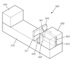
도 4는 본 발명의 다른 실시예에 따른 고전자 이동도 트랜지스터(300)를 도시한 것이다. 도 5는 도 4의 평면도이다. 4 shows a high-
상기 고전자 이동도 트랜지스터(300)는 채널 공급층(320)과, 상기 채널 공급층(320) 상의 소스 전극(330)과 드레인 전극(340)을 포함한다. 도시되지는 않았지만, 상기 채널 공급층(320) 하부에 채널층이 더 구비될 수 있다. 상기 소스 전극(330)과 드레인 전극(340) 사이에 적어도 하나의 채널 공핍층을 포함한다. 상기 적어도 하나의 채널 공핍층은 서로 이격되게 배열된 제1 채널 공핍층(350)과 제2 채널 공핍층(351)을 포함한다. 상기 제1 채널 공핍층(350)과 제2 채널 공핍층(351) 사이에 제3 채널 공핍층(352)이 구비되고, 상기 제1 채널 공핍층(350)으로부터 연장 돌출된 제4 채널 공핍층(353)이 구비될 수 있다. 상기 제2 채널 공급층(351) 상에 게이트 전극(360)이 구비된다. 상기 게이트 전극(360)으로부터 제1컨택(또는, 게이트 컨택)(361)이 연장 돌출되어 있다. 상기 제1컨택(361)은 상기 제3 채널 공핍층(352)의 일부 영역까지 연장될 수 있다. 제4 채널 공핍층(353) 상에 제2컨택(또는, 소스 컨택)(363)이 구비될 수 있다. 그리고, 상기 제3 채널 공핍층(352)과 제4 채널 공핍층(353) 사이에 상기 제1컨택(361)과 제2컨택(353)이 접촉되지 않는 영역에 브릿지(357)가 구비될 수 있다. The high
예를 들어, 상기 제3 채널 공핍층(352)과 게이트 컨택(361) 사이의 접촉 면적과 상기 제4 채널 공핍층(353)과 소스 컨택(363) 사이의 접촉 면적의 비가 일정한 값을 가질 때, 게이트 전극(360)과 제1채널 공핍층(351) 사이의 제1임피던스(또는, 게이트 임피던스)와 상기 소스 전극(330)과 제4 채널 공핍층(353) 사이의 제2임피던스(또는, 소스 임피던스)의 비가 일정한 값을 가질 수 있다. 예를 들어, 제1임피던스와 제2임피던스의 비가 0.1-10 범위를 가질 수 있으며, 상기 제3 채널 공핍층(352)과 게이트 컨택(361) 사이의 접촉 면적과 상기 제4 채널 공핍층(353)과 소스 컨택(363) 사이의 접촉 면적의 비를 조절하여 제1임피던스와 제2임피던스의 비를 조절할 수 있다. For example, when the ratio of the contact area between the third
상술한 바와 같이, 게이트 임피던스와 소스 임피던스 비가 일정한 값을 같도록 함으로써, 동작 주파수에 관계 없이 높은 문턴 전압이 일정하게 유지되도록 할 수 있다. As described above, by making the gate impedance and the source impedance ratio equal to a constant value, it is possible to maintain a high munturn voltage regardless of the operating frequency.
본 발명의 실시예에 따른 고전자이동도 트렌지스터는 이해를 돕기 위하여 도면에 도시된 실시예를 참고로 설명되었으나, 이는 예시적인 것에 불과하며, 당해 분야에서 통상적 지식을 가진 자라면 이로부터 다양한 변형 및 균등한 타 실시예가 가능하다는 점을 이해할 것이다. 따라서, 본 발명의 진정한 기술적 보호 범위는 첨부된 특허청구범위에 의해 정해져야 할 것이다. The high-mobility mobility transistor according to the embodiment of the present invention has been described with reference to the embodiment shown in the drawings to aid understanding, but this is merely exemplary, and those skilled in the art can make various modifications and variations therefrom. It will be understood that other equivalent embodiments are possible. Therefore, the true technical protection scope of the present invention should be defined by the appended claims.
110...채널층, 120,320...채널 공급층
130,330...소스 전극, 140,340...드레인 전극
150,350,351,352,353...채널 공핍층, 110 ... channel layer, 120,320 ... channel supply layer
130,330 ... source electrode, 140,340 ... drain electrode
150,350,351,352,353 ... channel depletion layer,
Claims (12)
상기 채널층 상의 채널 공급층;
상기 채널층 또는 채널 공급층 상에 서로 이격되게 배치된 소스 전극과 드레인 전극;
상기 채널 공급층 상에 마련되는 것으로, 상기 2차원 전자가스에 공핍 영역(depletion region)을 형성하는 채널 공핍층;
상기 채널 공핍층의 적어도 일부에 결합된 게이트 전극; 및
상기 채널 공핍층과 소스 전극을 연결하는 적어도 하나의 브릿지;를 포함하고,
상기 게이트 전극과 채널 공핍층 사이의 제1임피던스와 상기 소스 전극과 채널 공핍층 사이의 제2임피던스의 비가 일정한 값을 가지는 고전자 이동도 트랜지스터.A channel layer including two-dimensional electron gas;
A channel supply layer on the channel layer;
A source electrode and a drain electrode spaced apart from each other on the channel layer or the channel supply layer;
A channel depletion layer provided on the channel supply layer to form a depletion region in the two-dimensional electron gas;
A gate electrode coupled to at least a portion of the channel depletion layer; And
And at least one bridge connecting the channel depletion layer and a source electrode.
A high-electron mobility transistor having a constant ratio between the first impedance between the gate electrode and the channel depletion layer and the second impedance between the source electrode and the channel depletion layer.
상기 제1임피던스와 제2임피던스의 비가 0.1-10 범위를 가지는 고전자 이동도트랜지스터.According to claim 1,
A high-electron mobility transistor having a ratio of the first impedance to the second impedance in the range of 0.1-10.
상기 제1임피던스와 제2임피던스의 비가 동작 주파수에 관계없이 일정한 값을 가지는 고전자 이동도 트랜지스터.According to claim 1,
A high-electron mobility transistor having a constant value of the ratio of the first impedance to the second impedance regardless of the operating frequency.
상기 제1임피던스와 제2임피던스의 비가 1KHz-1GHz 범위의 동작 주파수에서 일정한 고전자 이동도 트랜지스터. According to claim 1,
A high-electron mobility transistor in which the ratio of the first impedance to the second impedance is constant at an operating frequency in a range of 1 KHz-1 GHz.
상기 제1임피던스는 게이트 전극과 채널 공핍층 사이의 제1컨덕턴스(GG), 게이트 전극과 채널 공핍층 사이의 제1캐패시턴스(CG), 게이트 전극과 채널 공핍층 사이의 제1저항(RG)을 포함하고, 상기 제2임피던스는 소스 전극과 채널 공핍층 사이의 제2컨덕턴스(GS), 소스 전극과 채널 공핍층 사이의 제2캐피시턴스(CG), 소스 전극과 채널 공핍층 사이의 제2 저항(RS)을 포함하며, 다음 식을 만족하는 고전자 이동도 트랜지스터.
<식>
GS/GG=CS/CG=RG/RS The method according to any one of claims 1 to 4,
The first impedance may include a first conductance (GG) between the gate electrode and the channel depletion layer, a first capacitance (CG) between the gate electrode and the channel depletion layer, and a first resistance (RG) between the gate electrode and the channel depletion layer. Including, the second impedance is the second conductance (GS) between the source electrode and the channel depletion layer, the second capacitance (CG) between the source electrode and the channel depletion layer, the second between the source electrode and the channel depletion layer A high-electron mobility transistor that includes a resistor (RS) and satisfies the following equation.
<Expression>
GS / GG = CS / CG = RG / RS
상기 게이트 전극과 채널 공핍층 사이에 제1컨택이 구비되고, 상기 소스 전극과 채널 공핍층 사이에 제2컨택과 브릿지가 구비된 고전자 이동도 트랜지스터. The method according to any one of claims 1 to 4,
A high electron mobility transistor having a first contact between the gate electrode and a channel depletion layer, and a second contact and a bridge between the source electrode and the channel depletion layer.
상기 제1컨택과 제2컨택은 금속으로 형성된 고전자 이동도 트랜지스터.The method of claim 6,
The first contact and the second contact are high electron mobility transistors formed of metal.
상기 제1컨택과 제2컨택은 반도체 또는 절연체로 형성된 고전자 이동도 트랜지스터.The method of claim 6,
The first contact and the second contact are high electron mobility transistors formed of a semiconductor or an insulator.
상기 채널 공핍층이 이격되게 배치된 제1 채널 공핍층과 제2 채널 공핍층, 상기 제1 채널 공급층과 제2 채널 공핍층 사이에 배치된 제3 채널 공핍층, 상기 제1 채널 공핍층으로부터 돌출 연장된 제4 채널 공핍층을 포함하는 고전자 이동도 트랜지스터.The method of claim 6,
From the first channel depletion layer and the second channel depletion layer, the channel depletion layer is spaced apart, the third channel depletion layer disposed between the first channel supply layer and the second channel depletion layer, from the first channel depletion layer A high electron mobility transistor comprising a protruding extended fourth channel depletion layer.
상기 제1컨택이 제1게이트 전극으로부터 상기 제3 채널 공핍층 위로 돌출 연장된 고전자 이동도 트랜지스터. The method of claim 9,
A high electron mobility transistor in which the first contact protrudes from the first gate electrode onto the third channel depletion layer.
상기 제2컨택이 상기 제4 채널 공핍층 위에 구비된 고전자 이동도 트랜지스터.The method of claim 10,
A high-electron mobility transistor in which the second contact is provided on the fourth channel depletion layer.
상기 제1컨택과 제3 채널 공핍층 사이의 접촉 면적과 상기 제2컨택과 제4 채널 공핍층 사이의 접촉 면적의 비에 의해 제1임피던스와 제2임피던스의 비가 결정되는 고전자 이동도 트랜지스터.The method of claim 11,
A high-electron mobility transistor in which the ratio of the first impedance and the second impedance is determined by the ratio of the contact area between the first contact and the third channel depletion layer and the contact area between the second contact and the fourth channel depletion layer.
Priority Applications (2)
| Application Number | Priority Date | Filing Date | Title |
|---|---|---|---|
| KR1020130124169A KR102100928B1 (en) | 2013-10-17 | 2013-10-17 | High electron mobility transistor |
| US14/330,072 US9252253B2 (en) | 2013-10-17 | 2014-07-14 | High electron mobility transistor |
Applications Claiming Priority (1)
| Application Number | Priority Date | Filing Date | Title |
|---|---|---|---|
| KR1020130124169A KR102100928B1 (en) | 2013-10-17 | 2013-10-17 | High electron mobility transistor |
Publications (2)
| Publication Number | Publication Date |
|---|---|
| KR20150044741A KR20150044741A (en) | 2015-04-27 |
| KR102100928B1 true KR102100928B1 (en) | 2020-05-15 |
Family
ID=52825434
Family Applications (1)
| Application Number | Title | Priority Date | Filing Date |
|---|---|---|---|
| KR1020130124169A Active KR102100928B1 (en) | 2013-10-17 | 2013-10-17 | High electron mobility transistor |
Country Status (2)
| Country | Link |
|---|---|
| US (1) | US9252253B2 (en) |
| KR (1) | KR102100928B1 (en) |
Families Citing this family (9)
| Publication number | Priority date | Publication date | Assignee | Title |
|---|---|---|---|---|
| US9660062B2 (en) * | 2015-04-30 | 2017-05-23 | Semiconductor Components Industries, Llc | Bidirectional HEMT and an electronic package including the bidirectional HEMT |
| GB2564482B (en) | 2017-07-14 | 2021-02-10 | Cambridge Entpr Ltd | A power semiconductor device with a double gate structure |
| US11336279B2 (en) | 2017-07-14 | 2022-05-17 | Cambridge Enterprise Limited | Power semiconductor device with a series connection of two devices |
| US11257811B2 (en) | 2017-07-14 | 2022-02-22 | Cambridge Enterprise Limited | Power semiconductor device with an auxiliary gate structure |
| US12382651B2 (en) | 2019-05-07 | 2025-08-05 | Cambridge Gan Devices Limited | Power semiconductor device with an auxiliary gate structure |
| US11955478B2 (en) * | 2019-05-07 | 2024-04-09 | Cambridge Gan Devices Limited | Power semiconductor device with an auxiliary gate structure |
| CN113994481B (en) * | 2019-06-17 | 2024-07-05 | 苏州晶湛半导体有限公司 | A semiconductor structure and a method for manufacturing the same |
| CN111863948B (en) * | 2020-08-03 | 2024-05-28 | 南京集芯光电技术研究院有限公司 | A GaN-based P-GaN enhanced HEMT device with a gate-source bridge and a method for preparing the same |
| CN112259605B (en) * | 2020-10-22 | 2022-08-23 | 东南大学 | Heterojunction semiconductor device resistant to instantaneous current impact |
Citations (1)
| Publication number | Priority date | Publication date | Assignee | Title |
|---|---|---|---|---|
| JP2013191868A (en) | 2006-11-20 | 2013-09-26 | Panasonic Corp | Semiconductor device |
Family Cites Families (48)
| Publication number | Priority date | Publication date | Assignee | Title |
|---|---|---|---|---|
| JP2924239B2 (en) * | 1991-03-26 | 1999-07-26 | 三菱電機株式会社 | Field effect transistor |
| JP3180776B2 (en) * | 1998-09-22 | 2001-06-25 | 日本電気株式会社 | Field-effect transistor |
| JP2000349096A (en) * | 1999-06-01 | 2000-12-15 | Matsushita Electric Ind Co Ltd | Compound field effect transistor and method of manufacturing the same |
| US6982204B2 (en) * | 2002-07-16 | 2006-01-03 | Cree, Inc. | Nitride-based transistors and methods of fabrication thereof using non-etched contact recesses |
| JP4385205B2 (en) * | 2002-12-16 | 2009-12-16 | 日本電気株式会社 | Field effect transistor |
| US7501669B2 (en) * | 2003-09-09 | 2009-03-10 | Cree, Inc. | Wide bandgap transistor devices with field plates |
| US8174048B2 (en) * | 2004-01-23 | 2012-05-08 | International Rectifier Corporation | III-nitride current control device and method of manufacture |
| JP4041075B2 (en) * | 2004-02-27 | 2008-01-30 | 株式会社東芝 | Semiconductor device |
| US7550783B2 (en) * | 2004-05-11 | 2009-06-23 | Cree, Inc. | Wide bandgap HEMTs with source connected field plates |
| US7573078B2 (en) * | 2004-05-11 | 2009-08-11 | Cree, Inc. | Wide bandgap transistors with multiple field plates |
| JP2006032552A (en) * | 2004-07-14 | 2006-02-02 | Toshiba Corp | Nitride-containing semiconductor device |
| US7161194B2 (en) * | 2004-12-06 | 2007-01-09 | Cree, Inc. | High power density and/or linearity transistors |
| US11791385B2 (en) * | 2005-03-11 | 2023-10-17 | Wolfspeed, Inc. | Wide bandgap transistors with gate-source field plates |
| US7855401B2 (en) * | 2005-06-29 | 2010-12-21 | Cree, Inc. | Passivation of wide band-gap based semiconductor devices with hydrogen-free sputtered nitrides |
| EP1938385B1 (en) * | 2005-09-07 | 2014-12-03 | Cree, Inc. | Transistors with fluorine treatment |
| JP2007220895A (en) * | 2006-02-16 | 2007-08-30 | Matsushita Electric Ind Co Ltd | Nitride semiconductor device and manufacturing method thereof |
| US7388236B2 (en) * | 2006-03-29 | 2008-06-17 | Cree, Inc. | High efficiency and/or high power density wide bandgap transistors |
| JP5147197B2 (en) * | 2006-06-06 | 2013-02-20 | パナソニック株式会社 | Transistor |
| JP2008124374A (en) | 2006-11-15 | 2008-05-29 | Sharp Corp | Insulated gate field effect transistor |
| JP4695622B2 (en) * | 2007-05-02 | 2011-06-08 | 株式会社東芝 | Semiconductor device |
| JP4478175B2 (en) * | 2007-06-26 | 2010-06-09 | 株式会社東芝 | Semiconductor device |
| KR101008272B1 (en) * | 2008-09-25 | 2011-01-13 | 전자부품연구원 | Nitride-based high electron mobility transistors having normal-off characteristics and a method of manufacturing the same |
| US7898004B2 (en) * | 2008-12-10 | 2011-03-01 | Transphorm Inc. | Semiconductor heterostructure diodes |
| JP5564791B2 (en) * | 2008-12-26 | 2014-08-06 | 富士通株式会社 | Compound semiconductor device and manufacturing method thereof |
| DE102009018054B4 (en) * | 2009-04-21 | 2018-11-29 | Infineon Technologies Austria Ag | Lateral HEMT and method of making a lateral HEMT |
| US9064945B2 (en) * | 2009-10-30 | 2015-06-23 | Alpha And Omega Semiconductor Incorporated | Normally off gallium nitride field effect transistors (FET) |
| US20110210377A1 (en) | 2010-02-26 | 2011-09-01 | Infineon Technologies Austria Ag | Nitride semiconductor device |
| US8319256B2 (en) | 2010-06-23 | 2012-11-27 | Power Integrations, Inc. | Layout design for a high power, GaN-based FET |
| KR101720589B1 (en) * | 2010-10-11 | 2017-03-30 | 삼성전자주식회사 | E-mode High Electron Mobility Transistor and method of manufacturing the same |
| US9502312B2 (en) * | 2010-11-29 | 2016-11-22 | Qualcomm Incorporated | Area efficient field effect device |
| JP2011066464A (en) | 2011-01-06 | 2011-03-31 | Panasonic Corp | Field effect transistor |
| US8586997B2 (en) * | 2011-02-15 | 2013-11-19 | Sensor Electronic Technology, Inc. | Semiconductor device with low-conducting field-controlling element |
| KR20120120826A (en) * | 2011-04-25 | 2012-11-02 | 삼성전기주식회사 | Nitride semiconductor device and manufacturing method thereof |
| JP5739774B2 (en) * | 2011-09-13 | 2015-06-24 | トランスフォーム・ジャパン株式会社 | Compound semiconductor device and manufacturing method thereof |
| US8772833B2 (en) * | 2011-09-21 | 2014-07-08 | Electronics And Telecommunications Research Institute | Power semiconductor device and fabrication method thereof |
| US9543391B2 (en) * | 2011-10-19 | 2017-01-10 | Samsung Electronics Co., Ltd. | High electron mobility transistor having reduced threshold voltage variation and method of manufacturing the same |
| US8785944B2 (en) * | 2011-12-07 | 2014-07-22 | Samsung Electronics Co., Ltd. | High electron mobility transistor |
| JP2013197315A (en) * | 2012-03-19 | 2013-09-30 | Fujitsu Ltd | Semiconductor device and semiconductor device manufacturing method |
| CN104395993B (en) * | 2012-06-20 | 2017-09-19 | 独立行政法人产业技术综合研究所 | Semiconductor device |
| KR101927408B1 (en) * | 2012-07-20 | 2019-03-07 | 삼성전자주식회사 | High electron mobility transistor and method of manufacturing the same |
| US8847310B1 (en) * | 2012-07-31 | 2014-09-30 | Azure Silicon LLC | Power device integration on a common substrate |
| US9412881B2 (en) * | 2012-07-31 | 2016-08-09 | Silanna Asia Pte Ltd | Power device integration on a common substrate |
| JP2014072379A (en) * | 2012-09-28 | 2014-04-21 | Fujitsu Ltd | Compound semiconductor device and manufacturing method of the same |
| KR101946009B1 (en) * | 2012-10-11 | 2019-02-08 | 삼성전자주식회사 | High electron mobility transistor and method of driving the same |
| US8981381B2 (en) * | 2012-11-16 | 2015-03-17 | Vishay General Semiconductor Llc | GaN-based Schottky diode having dual metal, partially recessed electrode |
| KR101927410B1 (en) * | 2012-11-30 | 2018-12-10 | 삼성전자주식회사 | High electron mobility transistor and method of manufacturing the same |
| JP6174874B2 (en) * | 2013-03-15 | 2017-08-02 | ルネサスエレクトロニクス株式会社 | Semiconductor device |
| KR102065113B1 (en) * | 2013-05-01 | 2020-01-10 | 삼성전자주식회사 | High electron mobility transistor and method of driving the same |
-
2013
- 2013-10-17 KR KR1020130124169A patent/KR102100928B1/en active Active
-
2014
- 2014-07-14 US US14/330,072 patent/US9252253B2/en active Active
Patent Citations (1)
| Publication number | Priority date | Publication date | Assignee | Title |
|---|---|---|---|---|
| JP2013191868A (en) | 2006-11-20 | 2013-09-26 | Panasonic Corp | Semiconductor device |
Also Published As
| Publication number | Publication date |
|---|---|
| KR20150044741A (en) | 2015-04-27 |
| US9252253B2 (en) | 2016-02-02 |
| US20150108547A1 (en) | 2015-04-23 |
Similar Documents
| Publication | Publication Date | Title |
|---|---|---|
| KR102100928B1 (en) | High electron mobility transistor | |
| US11699751B2 (en) | Semiconductor device | |
| KR101922122B1 (en) | Normally off high electron mobility transistor | |
| KR102065113B1 (en) | High electron mobility transistor and method of driving the same | |
| JP6476114B2 (en) | III-nitride enhancement mode transistors with adjustable and high gate-source voltage ratings | |
| CN104134659B (en) | It is able to carry out the III-nitride transistor of avalanche energy processing | |
| CN103000682B (en) | Nitride compound semiconductor device | |
| CN110785836B (en) | Semiconductor device | |
| CN102623498A (en) | Semiconductor device | |
| CN105247680B (en) | multi-channel transistor | |
| TW201701468A (en) | Semiconductor device | |
| CN103311240A (en) | Overvoltage protection device for compound semiconductor field effect transistors | |
| KR102065114B1 (en) | Operating method of reducing current collapse of power device | |
| CN106373996B (en) | Semiconductor device | |
| TW201711188A (en) | Semiconductor device | |
| KR102005451B1 (en) | High Electron Mobility Transistor | |
| KR20150065068A (en) | High electron mobility transistor and Electronic Apparatus comprising the same | |
| WO2016151905A1 (en) | Nitride semiconductor device | |
| US20170207085A1 (en) | Horizontal semiconductor device | |
| KR20150044325A (en) | Electronic Apparatus comprising High electron mobility transistor | |
| CN106328703A (en) | Semiconductor device with a plurality of semiconductor chips |
Legal Events
| Date | Code | Title | Description |
|---|---|---|---|
| PA0109 | Patent application |
St.27 status event code: A-0-1-A10-A12-nap-PA0109 |
|
| PG1501 | Laying open of application |
St.27 status event code: A-1-1-Q10-Q12-nap-PG1501 |
|
| A201 | Request for examination | ||
| PA0201 | Request for examination |
St.27 status event code: A-1-2-D10-D11-exm-PA0201 |
|
| E902 | Notification of reason for refusal | ||
| PE0902 | Notice of grounds for rejection |
St.27 status event code: A-1-2-D10-D21-exm-PE0902 |
|
| P11-X000 | Amendment of application requested |
St.27 status event code: A-2-2-P10-P11-nap-X000 |
|
| P13-X000 | Application amended |
St.27 status event code: A-2-2-P10-P13-nap-X000 |
|
| E701 | Decision to grant or registration of patent right | ||
| PE0701 | Decision of registration |
St.27 status event code: A-1-2-D10-D22-exm-PE0701 |
|
| GRNT | Written decision to grant | ||
| PR0701 | Registration of establishment |
St.27 status event code: A-2-4-F10-F11-exm-PR0701 |
|
| PR1002 | Payment of registration fee |
St.27 status event code: A-2-2-U10-U11-oth-PR1002 Fee payment year number: 1 |
|
| PG1601 | Publication of registration |
St.27 status event code: A-4-4-Q10-Q13-nap-PG1601 |
|
| PR1001 | Payment of annual fee |
St.27 status event code: A-4-4-U10-U11-oth-PR1001 Fee payment year number: 4 |
|
| PR1001 | Payment of annual fee |
St.27 status event code: A-4-4-U10-U11-oth-PR1001 Fee payment year number: 5 |
|
| P22-X000 | Classification modified |
St.27 status event code: A-4-4-P10-P22-nap-X000 |
|
| PR1001 | Payment of annual fee |
St.27 status event code: A-4-4-U10-U11-oth-PR1001 Fee payment year number: 6 |
|
| P22-X000 | Classification modified |
St.27 status event code: A-4-4-P10-P22-nap-X000 |