JP5908369B2 - Light receiving device - Google Patents
Light receiving device Download PDFInfo
- Publication number
- JP5908369B2 JP5908369B2 JP2012177270A JP2012177270A JP5908369B2 JP 5908369 B2 JP5908369 B2 JP 5908369B2 JP 2012177270 A JP2012177270 A JP 2012177270A JP 2012177270 A JP2012177270 A JP 2012177270A JP 5908369 B2 JP5908369 B2 JP 5908369B2
- Authority
- JP
- Japan
- Prior art keywords
- light receiving
- degrees
- substrate
- mirror
- angle
- Prior art date
- Legal status (The legal status is an assumption and is not a legal conclusion. Google has not performed a legal analysis and makes no representation as to the accuracy of the status listed.)
- Expired - Fee Related
Links
Images


Landscapes
- Optical Couplings Of Light Guides (AREA)
- Optical Integrated Circuits (AREA)
- Light Receiving Elements (AREA)
Description
本発明は、受光デバイスに関し、より詳細には、光導波路部品から出力された光を受光する受光素子を、光導波路部品上に集積した受光デバイスに関する。 The present invention relates to a light receiving device, and more particularly to a light receiving device in which a light receiving element that receives light output from an optical waveguide component is integrated on the optical waveguide component.
近年、光ファイバ伝送の普及に伴い、多数の光機能素子を高密度に集積する技術が求められており、その一つとして、石英系平面光波回路(以下、PLC)が知られている。PLCは低損失、高信頼性、高い設計自由度といった優れた特徴を有する導波路型光デバイスであり、実際に光通信伝送端における伝送装置には合分波器、分岐・結合器等の機能を集積したPLCが搭載されている。また、伝送装置内にはPLC以外の光デバイスとして、光と電気の信号を変換するフォトダイオード(以下、PD)や、レーザーダイオードなどの光デバイスも搭載されている。さらなる通信容量の拡大に向けて、光信号処理を行うPLC等の導波路型光デバイスと光電変換を行うPD等の光デバイスを集積した高機能な光電子集積型デバイスが求められている。このような集積型光デバイスのプラットフォームとしてPLCは有望であり、個別に作製したPDチップとPLCチップをハイブリッドに集積した光電子集積型デバイスが提案されている(例えば、特許文献1参照)。この例では、導波路の一部の領域に45度ミラーを設け、その導波路上にPDを実装することで、光導波路を伝搬する光をミラーで垂直に光路変換し、PDとの光結合を行う方法が採用されている。このようなPLC上に光結合用ミラーとPDを実装する集積型の受光デバイス構造は、デバイスの小型化、および光波回路設計自由度の面で利点がある。このとき、実際にPDを実装するためにはPLC上にPDを何らかの方法で接合すると同時に電気的に接続する必要がある。一般的に、裏面入射型の面PDの場合は通信波長の透過性が高い接着剤でPDの基板側を接合、ワイヤボンディング等で表面のPD電極と接続し、表面入射型の面PDの場合はPLC側に設けた電極に対してバンプ接続することで接合を同時に行う。その結果、導波路から出射されたビームはミラーで光路変換された後、クラッドを透過して、PD基板またはバンプの距離を経た後、PDと光結合する。ビームは導波路からの出射時に回折され、光結合距離が長くなるほどビームが拡がるため、効率的に光結合可能な大口径の低速PD(〜数GHz)をハイブリッド集積した受光デバイスは光強度モニタ用途に限られていた。一方で、高速なPD(〜数十GHz)を集積するには小口径(例えば20μm以下)のPD受光部に対し、レンズ等の光学素子で集光する必要がある。その結果、導波路・PD間の光結合距離が長くなるため、高速な受光デバイスでは小型化が困難になる。このように受光デバイスのハイブリッド集積において小型化と高速化は相反する事項であり、これらを両立することでより高機能化が可能な受光デバイスの実現が課題であった。 In recent years, with the spread of optical fiber transmission, a technique for integrating a large number of optical functional elements at a high density has been demanded. As one of them, a quartz-based planar lightwave circuit (hereinafter, PLC) is known. The PLC is a waveguide type optical device with excellent characteristics such as low loss, high reliability, and high design flexibility. Actually, the transmission equipment at the optical communication transmission end has functions such as multiplexer / demultiplexer, branch / coupler, etc. A PLC in which is integrated is mounted. In addition, in the transmission apparatus, as an optical device other than the PLC, an optical device such as a photodiode (hereinafter referred to as PD) for converting a signal between light and electricity and a laser diode is mounted. For further expansion of communication capacity, a highly functional optoelectronic integrated device in which a waveguide type optical device such as a PLC that performs optical signal processing and an optical device such as a PD that performs photoelectric conversion are integrated is required. PLC is promising as a platform for such an integrated optical device, and an optoelectronic integrated device in which a PD chip and a PLC chip manufactured individually are integrated in a hybrid has been proposed (for example, see Patent Document 1). In this example, a 45-degree mirror is provided in a partial region of the waveguide, and a PD is mounted on the waveguide so that light propagating through the optical waveguide is vertically converted by the mirror and optically coupled to the PD. The method of doing is adopted. Such an integrated light receiving device structure in which the optical coupling mirror and the PD are mounted on the PLC is advantageous in terms of downsizing of the device and freedom in designing the lightwave circuit. At this time, in order to actually mount the PD, it is necessary to join the PD on the PLC by some method and to make an electrical connection at the same time. In general, in the case of a back-illuminated surface PD, the substrate side of the PD is bonded with an adhesive having a high transmission wavelength, and the surface PD electrode is connected by wire bonding or the like. Are simultaneously joined by bump connection to the electrodes provided on the PLC side. As a result, the beam emitted from the waveguide is optically converted by a mirror, passes through the cladding, passes through the distance of the PD substrate or bump, and is optically coupled to the PD. The beam is diffracted when exiting from the waveguide, and the beam expands as the optical coupling distance increases. Therefore, a light-receiving device that hybridizes a large-diameter low-speed PD (up to several GHz) that can be optically coupled efficiently is used for light intensity monitoring. It was limited to. On the other hand, in order to integrate high-speed PD (up to several tens of GHz), it is necessary to collect light with an optical element such as a lens with respect to a PD light receiving unit having a small aperture (for example, 20 μm or less). As a result, since the optical coupling distance between the waveguide and the PD becomes long, it is difficult to reduce the size of the high-speed light receiving device. Thus, in the hybrid integration of light receiving devices, downsizing and speeding up are contradictory matters, and it has been a challenge to realize a light receiving device capable of achieving higher functions by satisfying these requirements.
この課題に対し、光結合距離を究極まで縮めることで、高速PDへの高効率光結合を可能にする集積技術としてヘテロジニアス集積がある(例えば、非特許文献1、非特許文献2参照)。上記の受光デバイスでは、PLC表面上へのPD実装構造として、PD基板、バンプ等のPD本来の機能以外の部分が含まれており、光結合距離が数百μmオーダーと、長くなる原因となっていた。レンズ等を用いずに高速PDを集積し、光結合距離を短くするには、PDの機能部分、つまり光半導体のエピタキシャル層からなるPD構造のみがPLC表面に接合された構造が望ましい。ヘテロジニアス集積技術は異なる材料同士を接合した後、プラットフォーム基板上でデバイスを作製するプロセスから成る異種材料融合集積技術であり、この技術を用いることで上記の構造を実現可能である。具体的には、光半導体エピタキシャル層を形成した基板をフェイスダウンでPLCのオーバークラッド表面に接合し、基板を研磨やエッチング等で除去することで、エピタキシャル層のみがPLC表面上に接合された状態とする。この状態でフォトリソグラフィーおよびエッチングのような一般的な光半導体加工プロセスでPD構造を形成する工程を経て、基板やバンプを除いた必要な部分のみでPD構造106が集積される(図1)。高効率な光結合には、PLCとエピタキシャル層を薄い層(〜1μm)で接合する必要があるため、ダイレクトボンディングや樹脂による接着が用いられる。こうすることで、30μm以下の光結合距離で低損失な光結合を実現できると共に、レンズ等が不要であるため小型化が可能である。また、異種材料を接合し、プラットフォーム基板上で光デバイスを作製するプロセスは、材料的にPLC自体が本来持たない光半導体の機能を高密度に集積できる。さらに、ハイブリッド集積では集積するそれぞれの光デバイス間で精密な光学実装が必要なのに対し、ヘテロジニアス集積ではフォトリソグラフィプロセスを適用することで、一括で高精度にアライメントでき、高スループットな光デバイスを作製できる。 In response to this problem, there is heterogeneous integration as an integration technology that enables high-efficiency optical coupling to a high-speed PD by reducing the optical coupling distance to the ultimate (see, for example, Non-Patent Document 1 and Non-Patent Document 2). In the above light receiving device, the PD mounting structure on the PLC surface includes portions other than the original functions of the PD such as a PD substrate and a bump, which causes the optical coupling distance to become as long as several hundred μm. It was. In order to integrate high-speed PDs without using a lens or the like and shorten the optical coupling distance, a structure in which only a PD functional part, that is, a PD structure composed of an epitaxial layer of an optical semiconductor is bonded to the PLC surface is desirable. The heterogeneous integration technology is a heterogeneous material integration technology that consists of a process of manufacturing devices on a platform substrate after bonding different materials, and the above structure can be realized by using this technology. Specifically, the substrate on which the optical semiconductor epitaxial layer is formed is bonded face-down to the PLC overcladding surface, and the substrate is removed by polishing, etching, or the like, so that only the epitaxial layer is bonded on the PLC surface. And In this state, the PD structure 106 is integrated only in necessary portions excluding the substrate and bumps through a process of forming the PD structure by a general optical semiconductor processing process such as photolithography and etching (FIG. 1). For high-efficiency optical coupling, since it is necessary to join the PLC and the epitaxial layer with a thin layer (˜1 μm), direct bonding or resin bonding is used. In this way, low-loss optical coupling can be realized with an optical coupling distance of 30 μm or less, and miniaturization is possible because a lens or the like is unnecessary. In addition, the process of bonding dissimilar materials and manufacturing an optical device on a platform substrate can integrate the functions of an optical semiconductor that the PLC itself does not originally have in high density. In addition, in the case of hybrid integration, precise optical mounting is required between each integrated optical device, whereas in heterogeneous integration, high-throughput optical devices can be manufactured by applying high-precision alignment by applying a photolithography process. it can.
しかしながら、光結合距離を短くすることで、従来のハイブリッド集積よりも通信用受光デバイスとして好ましくない反射戻り光が発生し易い。これは、導波路から出射されたビームの一部がPD表面等の屈折率界面で反射され、ミラーを介して逆方向にPLC内へ戻ってくるとき、ビームの一部が導波路に結合することで発生する。上記のヘテロジニアス集積型受光デバイス構造は光結合距離が短く、戻ってくるビーム径が小さいため、その結果、導波路への反射戻り光の結合が増加する。反射戻り光は光信号の伝送品質に大きく影響することから、特に光通信システムに適用する場合、30dB以上損失させることが求められる。この反射戻り光を低減する手法として、屈折率界面に対するビームの入射角を8度以上にすることで、戻り光損失を増加させる方法が一般的である。 However, by shortening the optical coupling distance, reflected return light which is not preferable as a light receiving device for communication is more likely to be generated than the conventional hybrid integration. This is because when a part of the beam emitted from the waveguide is reflected at the refractive index interface such as the PD surface and returns to the PLC in the reverse direction via the mirror, a part of the beam is coupled to the waveguide. Occurs. The above heterogeneous integrated light-receiving device structure has a short optical coupling distance and a small returning beam diameter. As a result, the coupling of reflected return light to the waveguide increases. Since the reflected return light greatly affects the transmission quality of the optical signal, it is required to lose 30 dB or more particularly when applied to an optical communication system. As a method of reducing the reflected return light, a method of increasing the return light loss by setting the incident angle of the beam to the refractive index interface to be 8 degrees or more is common.
図2に、基板203とミラー面のなす角(ミラー傾斜角θ205)が、45度±8度以上となる受光デバイスの一例を示す。受光デバイスでも、ミラー傾斜角θ205を45度から±8度以上傾けることで同様の効果が得られる。しかし、入射角を大きくするにつれて透過率の偏波依存性が大きくなり、その結果、偏波依存性損失(以下、PDL)が増加し、受光特性が損なわれる。このように、ヘテロジニアス集積型受光デバイスでは、高速PDを小型かつ低損失に集積し、高機能な受光デバイスを実現できる一方で、相反する問題である反射戻り光の低減とPDLの低減の両立が課題となっている。
FIG. 2 shows an example of a light receiving device in which the angle formed by the
本発明は、このような問題に鑑みてなされたもので、その目的とするところは、フォトダイオードの表面実装において、光路変換による光導波路素子と光素子間の光信号入出力に伴い発生する反射戻り光および光結合の偏波依存性を、結合損失を増加させることなく低減させる受光デバイスを提供することにある。 The present invention has been made in view of such a problem, and an object of the present invention is a reflection that occurs in the surface mounting of a photodiode due to optical signal input / output between the optical waveguide element and the optical element by optical path conversion. An object of the present invention is to provide a light receiving device that reduces the polarization dependence of return light and optical coupling without increasing coupling loss.
本発明は、このような目的を達成するために、請求項1に記載の発明は、基板と、前記基板上に設けられ、コアおよびクラッドからなる光導波路と、前記コアの出射方向と交わり、前記基板の垂直方向に対して前記コアよりも深く形成された傾斜面と、前記傾斜面の少なくとも前記コアの前記出射方向と交わる領域に被着され、前記コアからの出射光の少なくとも一部が前記クラッドの上方に反射されたビームの軸方向が、前記基板の垂直方向から傾くように形成された反射膜とを備えた光導波路部品と、前記クラッドの上面に設けられ、前記クラッドの上方に反射された前記ビームを受光する受光素子とを備えた受光デバイスであって、前記傾斜面は、前記反射膜により、前記光導波路を導波してきた光が前記クラッドの上面方向に反射するように形成された傾斜角を有するとともに、前記基板の垂直方向から見て、前記傾斜面への前記光導波路の出力方向と前記傾斜面の法線からなる角度が0度よりも大きく、前記傾斜角、および、前記基板の垂直方向から見たときの、前記傾斜面への前記光導波路の出力方向と前記傾斜面の法線からなる角度が、前記光導波路中を導波する光と受光素子との結合効率の偏波依存性が抑制されるよう設定され、前記光導波路部品は、入力された光信号の偏波分離を行う偏波分離回路を含み、前記受光素子は、偏波分離された光信号のTE偏光を受光する第1の受光素子と、偏波分離された光信号のTM偏光を受光する第2の受光素子とを含み、前記偏波分離された光信号のTE偏光については、前記基板の水平方向に対する前記傾斜面の角度が60度から78度であり、かつ前記基板の垂直方向から見て、前記傾斜面への前記光導波路の出力方向と前記傾斜面の法線からなる角度が7度から17度であり、前記偏波分離された光信号のTM偏光については、前記基板の水平方向に対する前記傾斜面の角度が60度から78度であり、かつ前記基板の垂直方向から見て、前記傾斜面への前記光導波路の出力方向と前記傾斜面の法線からなる角度が4度以下であることを特徴とする。
In order to achieve such an object, the present invention according to claim 1 crosses a substrate, an optical waveguide provided on the substrate, and comprising a core and a clad, and an emission direction of the core. An inclined surface formed deeper than the core with respect to the vertical direction of the substrate, and at least a part of light emitted from the core is attached to a region intersecting at least the emission direction of the core of the inclined surface. An optical waveguide component including a reflective film formed so that an axial direction of a beam reflected above the clad is inclined from a vertical direction of the substrate; and provided on an upper surface of the clad; A light receiving device including a light receiving element for receiving the reflected beam, wherein the inclined surface reflects light guided through the optical waveguide toward the upper surface of the clad by the reflective film; The angle formed by the output direction of the optical waveguide to the inclined surface and the normal line of the inclined surface is greater than 0 degrees when viewed from the vertical direction of the substrate. A light and a light receiving element in which an angle and an angle formed by an output direction of the optical waveguide to the inclined surface and a normal line of the inclined surface when viewed from a direction perpendicular to the substrate are guided in the optical waveguide The optical waveguide component includes a polarization separation circuit that performs polarization separation of the input optical signal, and the light receiving element is polarization-separated. A first light receiving element that receives the TE polarized light of the optical signal and a second light receiving element that receives the TM polarized light of the polarization separated optical signal, and the TE polarization of the polarization separated optical signal The angle of the inclined surface with respect to the horizontal direction of the substrate is When viewed from the vertical direction of the substrate, the angle formed between the output direction of the optical waveguide to the inclined surface and the normal of the inclined surface is 7 to 17 degrees. Regarding the TM polarization of the optical signal subjected to wave separation, the angle of the inclined surface with respect to the horizontal direction of the substrate is 60 degrees to 78 degrees, and the optical waveguide toward the inclined surface when viewed from the vertical direction of the substrate. The angle formed by the output direction and the normal line of the inclined surface is 4 degrees or less .
請求項2に記載の発明は、請求項1に記載の受光デバイスであって、前記受光素子は、基板材料が取り除かれた状態で前記クラッドの上面へ接合された光半導体エピタキシャル層により形成され、接着層によって前記クラッド上に接着され、並びに受光径20μm以下の受光部を有し、前記受光素子の受光面が前記反射膜を備えた前記傾斜面を介して、前記光導波路の前記コアと光学的に結合されたときの光強度分布の標準偏差の4倍が前記受光素子の前記受光径以下であることを特徴とする。
The invention according to
請求項3に記載の発明は、請求項1から請求項2のいずれか一項に記載の受光デバイスであって、前記光導波路がシリコン、あるいは石英系ガラスで形成されていることを特徴とする。
According to a third aspect of the invention, a light-receiving device according to any one of
以上説明したように、本発明によれば、出力導波路の端部に備えられたミラーを含む光導波路部品上に、出力された光信号の受信用光素子が集積された光デバイスにおいて、光結合効率を保持しながら、PDLと反射戻り光を簡便に抑制した光デバイスを提供することが可能となる。 As described above, according to the present invention, in an optical device in which an optical element for receiving an output optical signal is integrated on an optical waveguide component including a mirror provided at an end of an output waveguide, It is possible to provide an optical device that easily suppresses PDL and reflected return light while maintaining coupling efficiency.
以下、図面を参照しながら本発明の実施形態について詳細に説明する。 Hereinafter, embodiments of the present invention will be described in detail with reference to the drawings.
(発明の基本構成)
図3に、本発明の基本構成を示す。本発明の基本構成は、Si基板303と、光導波路部品であるPLCと、PDとを備える。
(Basic configuration of the invention)
FIG. 3 shows the basic configuration of the present invention. The basic configuration of the present invention includes a
PLCの光導波路は、コア301を包含したクラッド302とで構成されている。PLCはSi基板303上に形成され、PLCのコア301の出射端部を含むクラッド302には傾斜面304が形成されている。コア301の出射端部にかかる傾斜面304には、反射膜が被着されたミラーが形成されている。クラッド302の上面には、PD構造306が形成されており、PD構造306は、クラッド302とPDが接着するための接着面310と、2つのPD電極308にはさまれたPD受光部307とで構成されている。
The optical waveguide of the PLC is composed of a clad 302 including a
図3に示される具体的な方法として、Si基板303の面を基準として、PLC面内に作製するミラー傾斜角θ305を従来の45度から0〜20度程度(実施例における角度の詳細は後述する)傾け、かつ、基板垂直方向から見て、ミラーへの出力導波路とミラー傾斜面304の法線からなるミラー入射角φ311を従来の0度より大きい角度から45度程度(実施例における角度の詳細は後述する)まで適切に傾けることで、結合効率を低減させることなく、反射戻り光とPDLの低減を行う。ミラーとなる傾斜面304は、基板面303に対して導波路のコア301よりも深く形成され、導波路の出射方向と交わる領域に反射膜が被着される。これによりクラッド302の上方に反射された出射光の方向軸は基板垂直方向から傾き、クラッド表面に形成されたPDの受光部307に対して斜めに入射する。
As a specific method shown in FIG. 3, the mirror tilt angle θ 305 produced in the PLC plane is set to about 0 to 20 degrees from the conventional 45 degrees with respect to the surface of the Si substrate 303 (details of the angles in the embodiment are The mirror incident angle φ 311 composed of the normal of the output waveguide to the mirror and the mirror inclined
以上説明したように、本発明は、光導波路部品中にミラーとなる反射膜が被着された傾斜面を有し、そのミラー傾斜角θ305が基板面を基準として45度程度(実施例における角度の詳細は後述する)から傾いた角度で形成され、かつ、基板垂直方向から見て、ミラーへの出力導波路とミラー面の法線からなる角度をミラー入射角φ311とすると、ミラー入射角φ311が垂直(0度)から傾いた構造を特徴としている。ミラー入射角φ311が0度の場合、ミラー傾斜角θ305を45度程度から傾けていくと、上記の説明のように光結合の偏波依存性により、PDLが生じる。このとき、導波路を伝搬するTMモードとTEモードは、それぞれミラー反射面においてp波とs波に対応し、PDの受光面に対しても、p波とs波として入射する。それに対し、ミラー入射角φ311を0度から傾けることで、例えばTMモードはs波とp波の両方の成分としてミラー反射面に入射することになり、その結果、PD受光面に対してもp波とs波の両方の成分として入射する。ミラー入射角φ311を0度から傾けていくと、p波のTMモード成分が、はじめは減少してゆき、ある角度で半分となり、さらに減少してゼロになったところで再び増加に転じても元に戻ってゆく。一方、p波のTEモード成分においては逆の増減を示し、TMモードが減少するに応じてゼロから増加してゆくため、p波のTMモードとTEモード成分の和は一定となる。s波では上記のTMとTEが逆になった挙動を示し、ある角度でp波と同じようにTMモードとTEモード成分の比が1対1になる。ある角度のとき、p波はTMモード成分とTEモード成分の割合が1対1となり、s波もTMモード成分とTEモード成分の比率が1対1となる。逆にTMモード成分、TEモード成分を構成するp波とs波の割合を考えると、TMモード成分、TEモード成分ともs波とp波の割合は1対1となる。従って、s波とp波の偏波依存性があるが、TMモード成分、TEモード成分はそれぞれを同じだけ含んでいるのでTMモード成分、TEモード成分に対する偏波依存性(PDL)は生じないことになる。また、含まれるTM/TEモードの比を変えることができるため、TMモードをs波、TEモードをp波としてPDに入射することが可能である。さらにPDへの入射時に生じた反射光が再び導波路に結合することで戻り光が発生するが、本発明のようにPDへの入射角φ311を傾けることで、戻り光と導波路の結合軸と結合角をずらし、戻り光も同時に減少させることができる。 As described above, the present invention has an inclined surface on which a reflection film to be a mirror is deposited in an optical waveguide component, and the mirror inclination angle θ 305 is about 45 degrees with respect to the substrate surface (in the embodiment). If the angle between the output waveguide to the mirror and the normal to the mirror surface is the mirror incidence angle φ 311 when viewed from the substrate vertical direction, the mirror incidence angle is 311. It is characterized by a structure in which the angle φ 311 is inclined from the vertical (0 degree). When the mirror incident angle φ 311 is 0 degree, when the mirror tilt angle θ 305 is tilted from about 45 degrees, PDL occurs due to the polarization dependence of optical coupling as described above. At this time, the TM mode and the TE mode propagating in the waveguide correspond to the p wave and the s wave on the mirror reflection surface, respectively, and are also incident on the light receiving surface of the PD as the p wave and the s wave. On the other hand, by tilting the mirror incident angle φ 311 from 0 degrees, for example, the TM mode is incident on the mirror reflecting surface as both s wave and p wave components, and as a result, also on the PD light receiving surface. Incident as both p-wave and s-wave components. When the mirror incident angle φ 311 is tilted from 0 degree, the TM mode component of the p-wave decreases at first, halves at a certain angle, and further decreases to zero and then increases again. Go back to the original. On the other hand, the TE mode component of the p wave shows the opposite increase / decrease and increases from zero as the TM mode decreases, so the sum of the TM mode and TE mode component of the p wave becomes constant. In the s wave, the above TM and TE are reversed, and the ratio of the TM mode to the TE mode component becomes 1: 1 as in the p wave at a certain angle. At a certain angle, the ratio of the TM mode component to the TE mode component is 1: 1 for the p wave, and the ratio of the TM mode component to the TE mode component is 1: 1 for the s wave. Conversely, when considering the ratio of the p wave and the s wave constituting the TM mode component and the TE mode component, the ratio of the s wave and the p wave is 1: 1 for both the TM mode component and the TE mode component. Therefore, there is polarization dependency of the s wave and p wave, but since the TM mode component and the TE mode component contain the same amount, the polarization dependency (PDL) for the TM mode component and the TE mode component does not occur. It will be. Moreover, since the ratio of the TM / TE mode included can be changed, it is possible to enter the PD with the TM mode as the s wave and the TE mode as the p wave. Further, the reflected light generated upon incidence on the PD is coupled back to the waveguide to generate return light. By tilting the incident angle φ 311 to the PD as in the present invention, the coupling between the return light and the waveguide is performed. The return angle can be reduced simultaneously by shifting the axis and the coupling angle.
このようにミラー傾斜角およびミラー入射角を適切な角度に設定することで、PDLと反射戻り光を両方低減することが可能である。一方で、ミラー傾斜角や入射角を従来の値から傾けていくことで光結合距離が長くなり、結合損失が増加する恐れがあるため、従来の値から大きく外れることは望ましくない。したがって、特定のミラー傾斜角および入射角の範囲において、従来構造と同等の結合損失のまま、発明の効果を得ることが可能となる。このようなミラー構造の工夫により、従来の作製工程に制限を加えることなく、簡便に実施可能で、PDLと反射戻り光を同時に低減した、良好な特性の受光デバイスを提供することが可能となる。 Thus, by setting the mirror tilt angle and the mirror incident angle to appropriate angles, it is possible to reduce both PDL and reflected return light. On the other hand, since the optical coupling distance is increased and the coupling loss may be increased by tilting the mirror tilt angle and the incident angle from the conventional values, it is not desirable to deviate significantly from the conventional values. Therefore, it is possible to obtain the effects of the invention while maintaining the same coupling loss as that of the conventional structure in a specific mirror tilt angle and incident angle range. By devising such a mirror structure, it is possible to provide a light-receiving device with good characteristics that can be easily implemented without limiting the conventional manufacturing process and that simultaneously reduces PDL and reflected return light. .
(第1の実施形態)
図4に、本発明における、第1の実施形態を表す平面図を示す。本発明の第1の実施形態にかかる受光デバイスは、入力用光導波路401、光回路402、および複数の受光部404で構成される。
(First embodiment)
In FIG. 4, the top view showing 1st Embodiment in this invention is shown. The light receiving device according to the first embodiment of the present invention includes an input
光デバイスにおいて、入力用光導波路401に光回路402が接続され、複数の受光部404と光回路402が、複数の出力用光導波路403で接続されている。
In the optical device, an
光回路で光信号処理された光信号は、それぞれ出力用光導波路403を介して受光部404へ導波され、電気信号へ変換される。受光部の構造は、上記で説明したように、ヘテロジニアス集積により作製されたPDと導波路・PD間光結合のためのミラーで構成される。全体のチップサイズは縦15mm、横20mm(図4の平面図では、長方形型)である。本発明の効果を検証するため、上記の受光デバイス構成で、結合損失と反射戻り光を抑えつつ、本発明の構造を用いることにより、PDLを低減する検討を行った。具体的には、ミラー入射角度φを従来の0度から傾けた構造の受光部を設計し、ミラー傾斜角度θ依存性を光結合損失や反射戻り光損失およびPDLの評価を求めた。
The optical signals subjected to the optical signal processing by the optical circuit are respectively guided to the
はじめに受光デバイスの構造を示す。光導波路部品として、サイズが縦15mm、横20mmで、コア径4.5μm、オーバークラッド膜厚15.5μm、コアとクラッドの屈折率差1.5 %の直線導波路(401,403)がシリコン基板上に形成された石英系PLCを用いた。光入力はPLCの短辺(15mm)側に設けられた導波路から行い、ミラーとなる傾斜面は入力側導波路の反対側に形成する。光回路402としてスプリッタが設けられ、光信号はスプリッタで受光部404へと4分岐される。
First, the structure of the light receiving device is shown. As an optical waveguide component, a linear waveguide (401, 403) having a size of 15 mm in length and 20 mm in width, a core diameter of 4.5 μm, an overclad film thickness of 15.5 μm, and a refractive index difference of 1.5% between the core and the clad is silicon. A quartz PLC formed on the substrate was used. Optical input is performed from a waveguide provided on the short side (15 mm) side of the PLC, and an inclined surface serving as a mirror is formed on the opposite side of the input-side waveguide. A splitter is provided as the
図5に受光部404の構造を示す。受光部404の構造は、図3の構成と同様、Si基板503と、光導波路部品であるPLCと、PDとを備える。
FIG. 5 shows the structure of the
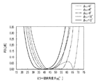
石英系PLCはシリコン基板503上に形成され、その光導波路のコア501端部には傾斜面504が形成されている。傾斜面504は、反射膜としてアルミが蒸着されており、コア501の傾斜面側から出射されたビームとPD受光部507を光結合するための光路変換ミラーとして機能する。形成される傾斜面504の角度(ミラー傾斜角θ505)は、基板面を基準として55度に設定した。このとき、基板垂直方向から見て、ミラーへの出力導波路とミラー面の法線からなるミラー入射角φ511を4つの受光部でそれぞれ異なった角度で設定し、6度、8度、10度、12度とした。コア501傾斜面端部の上方にはPD受光部507が(受光径19μm)、クラッド502上の膜厚0.8μm、屈折率1.55の樹脂からなる接着層510を介して接合されている。この石英系PLC上のもう一方の短辺(15mm)側に形成したPD構造506の位置は、上記のミラー角度に対して、最も結合効率の高くなるようにそれぞれ設計した。このとき、ビーム径を光強度分布の標準偏差の4倍とすると、反射されたビーム径はPD受光部において、10μm程度に拡大するが受光径に対して十分小さいため損失は発生しない。しかしながら、光結合距離が38μmより長くなるとビーム径が受光径より大きくなるため原理的に損失が発生するため、38μm以下であることが望ましい。このような構成により、コア501から出射されたビームは光路変換ミラーにより上方に、基板垂直軸から傾いた角度で反射される。反射されたビームはPD受光部507で受光される。
The quartz PLC is formed on the
次に上記の構造を作製するプロセスを示す。まず適切な工程により作製した石英系PLCを用意し、クラッド502上にエピタキシャル層508付きInP基板510の表面側を接合する。接合された後、基板510を研磨、ウェットエッチングにより除去することでエピタキシャル層508のみがPLC基板上に残る。この状態でエピタキシャル層を、フォトリソグラフィーおよび、エッチングにより加工することでPDを作製する。続いてドライエッチングにより深さが導波路より深くなるように傾斜面504を形成する(例えば、特許文献2参照)。なお、傾斜面の作製方法が、発明の効果を限定するものではないが、ドライエッチングにより作製することで高精度かつ自由度の高いミラーレイアウトが可能となる。続いて傾斜面に対し、蒸着またはスパッタなどにより金やアルミ等の金属を被着させ反射膜とし、ミラーを形成する。このとき、蒸着源、またはスパッタリングターゲットに対して基板表面を傾斜させることで、傾斜面に反射膜が成膜される。PDおよびミラーの位置は、設定したミラー角度に対して、最も結合効率が高くなるように、エッチングシフト等を考慮して設定する。こうすることでフォトマスクによってPDとミラー位置が一意に決まり、ハイブリッド集積のような高精度な位置合わせによる光学実装等が不要となる。
Next, a process for manufacturing the above structure will be described. First, a silica-based PLC prepared by an appropriate process is prepared, and the surface side of the
このような受光デバイスに波長1.55μmの光を入力したときのミラー傾斜角θ505に対する戻り光損失、結合損失、PDLの関係をそれぞれ図6、図7、図8に示す。図6、図7、図8には、従来のミラー入射角φ511=0度の場合も併せて示す。各材料界面での反射率、透過率、反射角、屈折角を計算し、導波路端から出射されて拡がったビームとPD受光面との結合、および戻り光と導波路との結合を求めた。 FIG. 6, FIG. 7 and FIG. 8 show the relationship between return light loss, coupling loss, and PDL with respect to the mirror tilt angle θ 505 when light having a wavelength of 1.55 μm is input to such a light receiving device. 6, 7, and 8 also show a conventional mirror incident angle φ 511 = 0 degree. The reflectance, transmittance, reflection angle, and refraction angle at each material interface were calculated, and the coupling between the beam emitted from the waveguide end and the PD receiving surface and the coupling between the return light and the waveguide were obtained. .
図7に示すように、ミラー入射角φ511=12度を除くと、今回のミラー傾斜角θ505が、55度を含む45度から60度の範囲で、各ミラー入射角φ511間で結合損失は0.5dB以下でほぼ一定であることがわかる。 As shown in FIG. 7, except for the mirror incident angle φ 511 = 12 degrees, the current mirror tilt angle θ 505 is coupled between the mirror incident angles φ 511 within the range of 45 degrees to 60 degrees including 55 degrees. It can be seen that the loss is almost constant at 0.5 dB or less.
また、図6より、ミラー傾斜角θ505を従来の45度から傾け、46.5度以上に設定することで反射戻り光損失が増加し、50dB以上の十分な損失が取れていることがわかる。 Further, from FIG. 6, it is understood that the reflected return light loss is increased by setting the mirror tilt angle θ 505 to 45.degree. Or more from the conventional 45.degree., And a sufficient loss of 50 dB or more can be obtained. .
一方、図8より従来のミラー入射角φ511=0度でミラー傾斜角θ505を45度から傾けていくと、PDLが増加する傾向が見られる。しかし今回の発明のように、ミラー入射角φ511を6度から10度の範囲で適切に設定することで、ミラー傾斜角θ505が46.5度から60度の範囲でもPDLを0.1dB以下に低減することが可能となる場合があることがわかる。例えば、今回のミラー傾斜角θ505=55度では、ミラー入射角φ511を傾けていくことでPDLが徐々に低減され、特にミラー入射角φ511=8度に設定することでPDLがほぼゼロになることがわかる。さらに、従来のミラー傾斜角θ505=45度の場合でも、ミラー入射角φ511を傾けることで反射戻り光損失を50dB以上に増加することができ、ミラー傾斜角θ505が43.5度から46.5度の範囲で、ミラー入射角φ511を6度から10度に設定することで、反射戻り光とPDLを低減する本発明の効果が得られる。 On the other hand, as shown in FIG. 8, when the mirror tilt angle θ 505 is tilted from 45 degrees with the conventional mirror incident angle φ 511 = 0 degrees, the PDL tends to increase. However, as in the present invention, by appropriately setting the mirror incident angle φ 511 within the range of 6 degrees to 10 degrees, the PDL can be reduced to 0.1 dB even when the mirror tilt angle θ 505 is within the range of 46.5 degrees to 60 degrees. It turns out that it may be possible to reduce the following. For example, in this mirror tilt angle theta 505 = 55 degrees, PDL is gradually reduced by gradually tilting the mirror incidence angle phi 511, in particular PDL approximately zero by setting the mirror incidence angle phi 511 = 8 degrees It turns out that it becomes. Further, even when the conventional mirror tilt angle θ 505 = 45 degrees, the reflected return light loss can be increased to 50 dB or more by tilting the mirror incident angle φ 511 , and the mirror tilt angle θ 505 is increased from 43.5 degrees. By setting the mirror incident angle φ 511 from 6 degrees to 10 degrees within the range of 46.5 degrees, the effect of the present invention for reducing reflected return light and PDL can be obtained.
このように、ミラー傾斜角θ505とミラー入射角φ511を適切に設定する今回の発明を用いることで反射戻り光と同時に、PDLも低減することが可能となり、低損失で良好な特性を持つ高機能な受光デバイスを提供できる。 As described above, by using the present invention in which the mirror tilt angle θ 505 and the mirror incident angle φ 511 are appropriately set, it is possible to reduce the PDL as well as the reflected return light, and have good characteristics with low loss. A highly functional light receiving device can be provided.
(第2の実施形態)
図9に、本発明における、第2の実施形態を示し、本発明の第2の実施形態にかかる受光デバイスは入力用光導波路901、光回路902、出力用光導波路903および905、受光部904および906で構成される。
(Second Embodiment)
FIG. 9 shows a second embodiment of the present invention. The light receiving device according to the second embodiment of the present invention includes an input
光デバイスにおいて、入力用光導波路901に光回路902が接続され、第1の受光部904と光回路902とが、第1の出力用光導波路903で接続され、第2の受光部906と光回路902とが、第2の出力用光導波路905で接続されている。
In the optical device, an
光回路902として偏波分離回路が形成され、TEおよびTMモードへと偏波分離される。TEモードは第1の出力用光導波路903を介して第1の受光部904へと導波され、一方、TMモードは第2の出力用光導波路905を介して第2の受光部906へと導波され、それぞれ電気信号へと変換される。受光部の構造は、上記で説明したヘテロジニアス集積により作製されるPDと導波路・PD間光結合のためのミラーで構成され、全体のチップサイズは縦19mm、横12mm(図9の平面図では、長方形型)である。本発明の効果を検証するため、上記の受光デバイス構成で、2つの受光部にそれぞれ別のミラー入射角を設定し、反射戻り光を抑えつつ、TEモードおよびTMモードの光結合損失を低減させる検討を行った。具体的にはいくつかのミラー傾斜角を設定したそれぞれの受光デバイスにおいてミラー入射角度を0度から傾けた構造の受光部を設計し、反射戻り光損失と、第1の受光部904におけるTEモードの光結合損失、および第2の受光部906におけるTMモードの光結合損失を求めた。
A polarization separation circuit is formed as the
はじめに受光デバイスの構造を示す。光導波路部品として、サイズが縦19mm、横12mmで、コア径4.2μm、オーバークラッド膜厚15.5μm、コアとクラッドの屈折率差2.5 %の直線導波路(901,903,905)がシリコン基板上に形成された石英系PLCを用いた。光入力はPLCの長辺(19mm)側に設けられた導波路から行い、ミラーとなる傾斜面は入力側導波路の反対側に形成する。光回路として、マッハツェンダー干渉計による偏波分離回路を設けた。マッハツェンダー干渉計の導波路アームにはλ/4波長板が挿入され、偏波間に位相差を設けることで、光信号をTEモードとTMモードに25dB以上の偏波消光比で分離する。その後、TEモードとTMモードはそれぞれ図10で示される構造の受光部へとそれぞれ導波される。 First, the structure of the light receiving device is shown. As an optical waveguide component, a linear waveguide (901, 903, 905) having a size of 19 mm long and 12 mm wide, a core diameter of 4.2 μm, an overcladding film thickness of 15.5 μm, and a refractive index difference of 2.5% between the core and the clad. Used a quartz-based PLC formed on a silicon substrate. Optical input is performed from a waveguide provided on the long side (19 mm) side of the PLC, and an inclined surface serving as a mirror is formed on the opposite side of the input-side waveguide. A polarization separation circuit using a Mach-Zehnder interferometer was provided as an optical circuit. A λ / 4 wave plate is inserted into the waveguide arm of the Mach-Zehnder interferometer, and a phase difference is provided between the polarized waves, so that the optical signal is separated into a TE mode and a TM mode with a polarization extinction ratio of 25 dB or more. Thereafter, the TE mode and the TM mode are respectively guided to the light receiving unit having the structure shown in FIG.
図10は、第1の受光部904、第2の受光部906の詳細図である。図10で示される構造では、4つのコア(1001、1002、1003、1004)を有するPLC上に4つのPDが集積されている。4つのPDは、それぞれPD構造(1005、1006、1007、1008)を有している。
FIG. 10 is a detailed view of the first
図11に第1の受光部904、第2の受光部906の構造を示す。第1の受光部904、第2の受光部906は、図3の構成と同様、Si基板1103と、光導波路部品であるPLCと、PDとを備える。
FIG. 11 shows the structure of the first
石英系PLCはSi基板1103上に形成され、その光導波路のコア1101端部には傾斜面1104が形成されている。傾斜面1104は、反射膜としてアルミが蒸着されており、コア1101の傾斜面側から出射されたビームとPD受光部1107を光結合するための光路変換ミラーとして機能する。形成される傾斜面1104の角度(ミラー傾斜角θ1105)を、基板面を基準として45度、66度、72度、78度の4水準に設定した。ミラー傾斜角はTEモード受光部、TMモード受光部で同じ角度である。また、基板垂直方向から見て、ミラーへの出力導波路とミラー面の法線からなる角をミラー入射角φ1111とした。コア1101傾斜面端部の上方にはPD受光部1107が(受光径20μm)、クラッド1102上の膜厚0.7μm、屈折率1.55の樹脂からなる接着層1110を介して接合されている。この石英系PLC上の短辺側に形成したPD構造1106の位置は、上記のミラー角度に対して、最も結合効率の高くなるようにそれぞれ設計した。このとき、ビーム径を光強度分布の標準偏差の4倍とすると、反射されたビーム径はPD受光部において、14μm程度に拡大するが受光径に対して十分小さいため損失は発生しない。しかしながら、光結合距離が30μmより長くなるとビーム径が受光径より大きくなるため原理的に損失が発生するため、30μm以下であることが望ましい。このような構成により、コア1101から出射されたビームは光路変換ミラーにより上方に、基板垂直軸から傾いた角度で反射される。反射されたビームはPD受光部1107で受光される。
The quartz PLC is formed on the
次に上記の構造を作製するプロセスを示す。まず適切な工程により作製した石英系PLCを用意し、クラッド上にエピタキシャル層付きInP基板の表面側を接合する。接合された後、基板を研磨、ウェットエッチングにより除去することでエピタキシャル層のみがPLC基板上に残る。この状態でエピタキシャル層を、フォトリソグラフィーおよび、エッチングにより加工することでPDを作製する。続いてドライエッチングにより深さが導波路より深くなるように傾斜面を形成する(例えば、特許文献2参照)。このとき、TE・TMモード受光部のミラーが一度に作製されるため、どちらも同じミラー傾斜角θ1105となる。なお、傾斜面の作製方法が、発明の効果を限定するものではないが、ドライエッチングにより作製することで、偏波ごとに異なるミラー入射角でのミラー作製が容易に実現できる。続いて傾斜面に対し、蒸着またはスパッタなどにより金やアルミ等の金属を被着させ反射膜とし、ミラーを形成する。このとき、蒸着源、またはスパッタリングターゲットに対して基板表面を傾斜させることで、傾斜面に反射膜が成膜される。PDおよびミラーの位置は、設定したミラー角度に対して、最も結合効率が高くなるように、エッチングシフト等を考慮して設定する。こうすることでフォトマスクによってPDとミラー位置が一意に決まり、ハイブリッド集積のような高精度な位置合わせによる光学実装等が不要となる。 Next, a process for manufacturing the above structure will be described. First, a quartz-based PLC prepared by an appropriate process is prepared, and the surface side of the InP substrate with an epitaxial layer is bonded onto the clad. After bonding, the substrate is polished and removed by wet etching, so that only the epitaxial layer remains on the PLC substrate. In this state, the epitaxial layer is processed by photolithography and etching to produce a PD. Subsequently, an inclined surface is formed by dry etching so that the depth becomes deeper than the waveguide (see, for example, Patent Document 2). At this time, since the mirrors of the TE / TM mode light receiving unit are fabricated at a time, both have the same mirror tilt angle θ 1105 . In addition, although the manufacturing method of an inclined surface does not limit the effect of invention, the mirror manufacture in the mirror incident angle which changes for every polarization | polarized-light can be easily implement | achieved by producing by dry etching. Subsequently, a metal such as gold or aluminum is deposited on the inclined surface by vapor deposition or sputtering to form a reflective film, thereby forming a mirror. At this time, the reflective film is formed on the inclined surface by inclining the substrate surface with respect to the vapor deposition source or the sputtering target. The positions of the PD and the mirror are set in consideration of an etching shift or the like so that the coupling efficiency becomes the highest with respect to the set mirror angle. In this way, the PD and mirror positions are uniquely determined by the photomask, and optical mounting by high-precision alignment such as hybrid integration becomes unnecessary.
このような受光デバイスに波長1.55μmの光を入力したときのミラー入射角φ1111に対する戻り光損失、TEモード受光部での光結合損失、TMモード受光部の光結合損失とPDLの計算値をそれぞれ図12、図13、図14に示す。各材料界面での反射率、透過率、反射角、屈折角を計算し、導波路端から出射されて拡がったビームとPD受光面との結合、および戻り光と導波路との結合を求めた。ここで、ミラー入射角φ1111は、TEモードに係るミラー入射角度の場合、φTEとし、TMモードに係るミラー入射角度の場合、φTMとする。 Return light loss with respect to the mirror incident angle φ 1111 when light having a wavelength of 1.55 μm is input to such a light receiving device, optical coupling loss at the TE mode light receiving portion, optical coupling loss at the TM mode light receiving portion, and calculated values of PDL Are shown in FIGS. 12, 13, and 14, respectively. The reflectance, transmittance, reflection angle, and refraction angle at each material interface were calculated, and the coupling between the beam emitted from the waveguide end and the PD receiving surface and the coupling between the return light and the waveguide were obtained. . Here, the mirror incident angle φ 1111 is φ TE in the case of the mirror incident angle related to the TE mode, and is φ TM in the case of the mirror incident angle related to the TM mode.
図12に示すように、ミラー傾斜角θ1105=45度の場合を除き、0度から25度のミラー入射角度φ1111で50dB以上の十分な反射戻り光損失が得られている。また、ミラー傾斜角θ1105=45度の場合でもミラー入射角度φ1111を6度以上傾けることで十分な反射戻り光損失が得られることが分かる。 As shown in FIG. 12, except for the case where the mirror tilt angle θ 1105 is 45 degrees, a sufficient reflected return light loss of 50 dB or more is obtained at a mirror incident angle φ 1111 of 0 degrees to 25 degrees. It can also be seen that even when the mirror tilt angle θ 1105 = 45 degrees, a sufficient reflected return light loss can be obtained by tilting the mirror incident angle φ 1111 by 6 degrees or more.
図13では、TEモード光結合損失のミラー入射角度φTE依存性が示されるが、どの入射角度においてもミラー入射角度φTEを傾けていく(大きくする)ことで結合損失が低減され、あるミラー傾斜角θ1105で最小値となり、再び増加する傾向が示される。ミラー傾斜角θ1105により、最小の結合損失の値と、そのときのミラー入射角φTEは異なるが、ミラー傾斜角θ1105が60度から78度の場合、ミラー入射角φTEが7度から17度の範囲で、0.4dB以下の低損失を達成できる場合があることがわかる。例えば、ミラー傾斜角θ1105が60度でミラー入射角φTEが10度から17度、ミラー傾斜角θ1105が66度でミラー入射角φTEが8度から16度、ミラー傾斜角θ1105が72度でミラー入射角φTEが7度から14度、ミラー傾斜角θ1105が78度でミラー入射角φTEが7度から9度である。特にミラー傾斜角θ1105が72度ではミラー入射角φTEが10度で、結合損失が0.15dB以下となる。これはTEモードがミラーで光路変換され、PDに入射されるときに、はじめはs波の成分のみであったのが、ミラー入射角φTEを変化させていくことでp波の成分が増加し、同時にPDへの入射角がブリュースター角に近づき、透過率が増加するためである。 FIG. 13 shows the dependence of the TE mode optical coupling loss on the mirror incident angle φ TE , but the coupling loss is reduced by tilting (increasing) the mirror incident angle φ TE at any incident angle, and a certain mirror The inclination angle θ 1105 shows a minimum value and a tendency to increase again. The mirror tilt angle theta 1105, the value of the minimum coupling loss, the mirror incidence angle phi TE when different, but if the mirror tilt angle theta 1105 is 78 degrees from 60 degrees, from the mirror incidence angle phi TE is 7 degrees It can be seen that a low loss of 0.4 dB or less may be achieved in the range of 17 degrees. For example, the mirror tilt angle θ 1105 is 60 degrees, the mirror incident angle φ TE is 10 degrees to 17 degrees, the mirror tilt angle θ 1105 is 66 degrees, the mirror incident angle φ TE is 8 degrees to 16 degrees, and the mirror tilt angle θ 1105 is At 72 degrees, the mirror incident angle φ TE is 7 degrees to 14 degrees, the mirror tilt angle θ 1105 is 78 degrees, and the mirror incident angle φ TE is 7 degrees to 9 degrees. In particular, when the mirror tilt angle θ 1105 is 72 degrees, the mirror incident angle φ TE is 10 degrees, and the coupling loss is 0.15 dB or less. This is the optical path conversion in a TE mode mirror, when it is incident on the PD, that initially was only component of the s-wave component of the p-wave is increased by gradually changing the mirror angle of incidence phi TE At the same time, the incident angle to the PD approaches the Brewster angle and the transmittance increases.
一方、TMモード光結合損失のミラー入射角度φTM依存性は図14に示される。ミラー傾斜角θ1105が45度の場合、ミラー入射角φTMを25度から29度の範囲に設定することで0.2dB近くまで低損失化可能だが、図13より、TEモード側を同程度に低損失化するのは困難であり、損失ばらつきが大きくなるという問題がある。一方でミラー傾斜角θ1105を大きくし、例えばミラー傾斜角θ1105を60度から78度に設定すると、ミラー入射角φTM=0度で損失が最小値となり、ミラー入射角φTMが0度から4度の間で0.4dB以下の低損失化が可能となる。特にミラー傾斜角θ1105が72度のとき、損失0.17dB以下となる。これらのミラー傾斜角度θ1105の場合は、同時にTEモード受光部側を同程度の損失になるようミラー入射角φTMを設定することで、ばらつきを発生させること無く低損失化ができる。このように、ミラー傾斜角θ1105とミラー入射角φTE、φTMを適切に設定することでTE・TMモードのどちらの偏波状態でも、反射戻り光損失を十分に取りつつ、結合損失を低減することが可能となる。特にミラー傾斜角θ1105を60度から78度の範囲に設定することで、どちらの偏波状態に対しても、従来より低損失な0.4dB以下の結合が可能となるTEモードのミラー入射角φTE(7度から14度(上記に挙げた条件を満たす角度))、およびTMモードのミラー入射角φTM(0度から4度)を設定することができる。今回の場合、ミラー傾斜角θ1105を72度に設定し、TEモード受光部およびTMモード受光部のミラー入射角度φTE、φTMをそれぞれ個別に設定することで、どちらの偏波でも最小の結合損失が得られる。 On the other hand, the dependency of the TM mode optical coupling loss on the mirror incident angle φ TM is shown in FIG. When the mirror tilt angle θ 1105 is 45 degrees, the loss can be reduced to nearly 0.2 dB by setting the mirror incident angle φ TM in the range of 25 degrees to 29 degrees. However, it is difficult to reduce the loss, and there is a problem that the loss variation becomes large. On the other hand, when the mirror tilt angle θ 1105 is increased, for example, when the mirror tilt angle θ 1105 is set from 60 degrees to 78 degrees, the loss is minimum when the mirror incident angle φ TM = 0 degrees, and the mirror incident angle φ TM is 0 degrees. From 4 degrees to 4 degrees, a loss of 0.4 dB or less can be achieved. In particular, when the mirror tilt angle θ 1105 is 72 degrees, the loss is 0.17 dB or less. In the case of these mirror tilt angles θ 1105 , the loss can be reduced without causing variations by setting the mirror incident angle φ TM so that the TE mode light receiving unit side has the same loss at the same time. As described above, by appropriately setting the mirror tilt angle θ 1105 and the mirror incident angles φ TE and φ TM , the coupling loss can be reduced while sufficiently taking the reflected return light loss in both the TE and TM mode polarization states. It becomes possible to reduce. In particular, by setting the mirror tilt angle θ 1105 in the range of 60 ° to 78 °, the TE mode mirror incidence that enables coupling of 0.4 dB or less with a lower loss than in the past is possible for both polarization states. An angle φ TE (7 to 14 degrees (an angle satisfying the above conditions)) and a TM mode mirror incident angle φ TM (0 to 4 degrees) can be set. In this case, the mirror tilt angle θ 1105 is set to 72 degrees, and the mirror incident angles φ TE and φ TM of the TE mode light receiving unit and the TM mode light receiving unit are set individually, so that the minimum polarization can be obtained for both polarizations. Coupling loss is obtained.
偏波分離素子や、偏波回転素子を光回路に含む受光デバイスにおいて、今回の発明を用いることで、反射戻り光と同時に、結合損失を低減することが可能となり、低損失で良好な特性を持つ高機能な受光デバイスを提供できる。 By using the present invention in a light receiving device that includes a polarization separation element and a polarization rotation element in the optical circuit, it becomes possible to reduce the coupling loss simultaneously with the reflected return light. A highly functional light receiving device can be provided.
101,201,301,501,1001,1002,1003,1004,1101 コア
102,202,302,502,1102 クラッド
103,203,303,503,1103 Si基板
104,204,304,504,1104 傾斜面
106,206,306,506,1005,1006,1007,1008,1106 PD構造
107,207,307,507,1107 PD受光部
108,208,308,508,1108 PD電極
109,209,309,509 ビーム反射方向
210,310,510,1110 接着層
401,901 入力用光導波路
402,902 光回路
403 出力用光導波路
404 受光部
903 第1の出力用光導波路
904 第1の受光部
905 第2の出力用光導波路
906 第2の受光部
101, 201, 301, 501, 1001, 1002, 1003, 1004, 1101
Claims (3)
前記基板上に設けられ、コアおよびクラッドからなる光導波路と、前記コアの出射方向と交わり、前記基板の垂直方向に対して前記コアよりも深く形成された傾斜面と、前記傾斜面の少なくとも前記コアの前記出射方向と交わる領域に被着され、前記コアからの出射光の少なくとも一部が前記クラッドの上方に反射されたビームの軸方向が、前記基板の垂直方向から傾くように形成された反射膜とを備えた光導波路部品と、
前記クラッドの上面に設けられ、前記クラッドの上方に反射された前記ビームを受光する受光素子とを備えた受光デバイスであって、
前記傾斜面は、前記反射膜により、前記光導波路を導波してきた光が前記クラッドの上面方向に反射するように形成された傾斜角を有するとともに、
前記基板の垂直方向から見て、前記傾斜面への前記光導波路の出力方向と前記傾斜面の法線からなる角度が0度よりも大きく、
前記傾斜角、および、前記基板の垂直方向から見たときの、前記傾斜面への前記光導波路の出力方向と前記傾斜面の法線からなる角度が、前記光導波路中を導波する光と受光素子との結合効率の偏波依存性が抑制されるよう設定され、
前記光導波路部品は、入力された光信号の偏波分離を行う偏波分離回路を含み、
前記受光素子は、偏波分離された光信号のTE偏光を受光する第1の受光素子と、偏波分離された光信号のTM偏光を受光する第2の受光素子とを含み、
前記偏波分離された光信号のTE偏光については、前記基板の水平方向に対する前記傾斜面の角度が60度から78度であり、かつ前記基板の垂直方向から見て、前記傾斜面への前記光導波路の出力方向と前記傾斜面の法線からなる角度が7度から17度であり、
前記偏波分離された光信号のTM偏光については、前記基板の水平方向に対する前記傾斜面の角度が60度から78度であり、かつ前記基板の垂直方向から見て、前記傾斜面への前記光導波路の出力方向と前記傾斜面の法線からなる角度が4度以下であることを特徴とする受光デバイス。 A substrate,
An optical waveguide comprising a core and a clad provided on the substrate; an inclined surface that intersects an emission direction of the core and is formed deeper than the core with respect to a vertical direction of the substrate; and at least the inclined surface The axial direction of the beam, which is attached to the region of the core intersecting with the emission direction and in which at least a part of the emission light from the core is reflected above the cladding, is formed so as to be inclined from the vertical direction of the substrate. An optical waveguide component comprising a reflective film;
A light receiving device provided on a top surface of the clad and comprising a light receiving element for receiving the beam reflected above the clad,
The inclined surface has an inclination angle formed so that the light guided through the optical waveguide is reflected by the reflective film toward the upper surface of the cladding,
When viewed from the vertical direction of the substrate, the angle formed between the output direction of the optical waveguide to the inclined surface and the normal line of the inclined surface is greater than 0 degrees,
The angle between the tilt angle and the output direction of the optical waveguide to the tilted surface when viewed from the direction perpendicular to the substrate and the normal of the tilted surface is light guided in the optical waveguide. The polarization dependency of the coupling efficiency with the light receiving element is set to be suppressed ,
The optical waveguide component includes a polarization separation circuit that performs polarization separation of an input optical signal,
The light receiving element includes a first light receiving element that receives TE polarized light of the polarization separated optical signal, and a second light receiving element that receives TM polarized light of the polarization separated optical signal,
Regarding the TE polarization of the optical signal subjected to polarization separation, the angle of the inclined surface with respect to the horizontal direction of the substrate is 60 degrees to 78 degrees, and when viewed from the vertical direction of the substrate, The angle formed by the output direction of the optical waveguide and the normal of the inclined surface is 7 degrees to 17 degrees,
For the TM polarization of the polarization separated optical signal, the angle of the inclined surface with respect to the horizontal direction of the substrate is 60 degrees to 78 degrees, and when viewed from the vertical direction of the substrate, An angle between an output direction of an optical waveguide and a normal line of the inclined surface is 4 degrees or less .
前記受光素子の受光面が前記反射膜を備えた前記傾斜面を介して、前記光導波路の前記コアと光学的に結合されたときの光強度分布の標準偏差の4倍が前記受光素子の前記受光径以下であることを特徴とする請求項1に記載の受光デバイス。 The light receiving element is formed of an optical semiconductor epitaxial layer bonded to the upper surface of the clad with the substrate material removed, and is adhered onto the clad by an adhesive layer, and has a light receiving portion with a light receiving diameter of 20 μm or less. ,
Four times the standard deviation of the light intensity distribution when the light receiving surface of the light receiving element is optically coupled to the core of the optical waveguide via the inclined surface provided with the reflective film is the light receiving element. The light receiving device according to claim 1, wherein the light receiving device is equal to or smaller than a light receiving diameter.
Receiving device according to any one of claims 2 to claim 1, characterized in that the optical waveguide is formed of silicon or quartz glass.
Priority Applications (1)
| Application Number | Priority Date | Filing Date | Title |
|---|---|---|---|
| JP2012177270A JP5908369B2 (en) | 2012-08-09 | 2012-08-09 | Light receiving device |
Applications Claiming Priority (1)
| Application Number | Priority Date | Filing Date | Title |
|---|---|---|---|
| JP2012177270A JP5908369B2 (en) | 2012-08-09 | 2012-08-09 | Light receiving device |
Publications (2)
| Publication Number | Publication Date |
|---|---|
| JP2014035486A JP2014035486A (en) | 2014-02-24 |
| JP5908369B2 true JP5908369B2 (en) | 2016-04-26 |
Family
ID=50284494
Family Applications (1)
| Application Number | Title | Priority Date | Filing Date |
|---|---|---|---|
| JP2012177270A Expired - Fee Related JP5908369B2 (en) | 2012-08-09 | 2012-08-09 | Light receiving device |
Country Status (1)
| Country | Link |
|---|---|
| JP (1) | JP5908369B2 (en) |
Families Citing this family (1)
| Publication number | Priority date | Publication date | Assignee | Title |
|---|---|---|---|---|
| JP6322059B2 (en) * | 2014-06-12 | 2018-05-09 | 日本電信電話株式会社 | Manufacturing method of optical device |
Family Cites Families (2)
| Publication number | Priority date | Publication date | Assignee | Title |
|---|---|---|---|---|
| JPH0333726A (en) * | 1989-06-30 | 1991-02-14 | Nippon Telegr & Teleph Corp <Ntt> | Polarized wave separating optical circuit |
| KR100802199B1 (en) * | 2006-05-25 | 2008-03-17 | 정경희 | Optical module and its manufacturing method |
-
2012
- 2012-08-09 JP JP2012177270A patent/JP5908369B2/en not_active Expired - Fee Related
Also Published As
| Publication number | Publication date |
|---|---|
| JP2014035486A (en) | 2014-02-24 |
Similar Documents
| Publication | Publication Date | Title |
|---|---|---|
| JP7325188B2 (en) | Photonic chip with integrated collimation structure | |
| CN110637246B (en) | Photonic chip with integrated collimation structure | |
| KR101744281B1 (en) | photonic integrated circuit comprising light turning micro mirror interior of optical waveguide and method of manufacturing thereof | |
| US7366379B2 (en) | Optical component for free-space optical propagation between waveguides | |
| US9482816B2 (en) | Radiation coupler | |
| US20070160324A1 (en) | Photonic input/output port | |
| EP2932320A1 (en) | Fiber optic coupler array | |
| US20120114293A1 (en) | Optical waveguide structure having angled mirror and lens | |
| WO2019244554A1 (en) | Planar lightwave circuit and optical device | |
| JP5908369B2 (en) | Light receiving device | |
| KR101063963B1 (en) | Optical power measurement module for flat optical waveguide device and manufacturing method thereof | |
| Romero-García et al. | Misalignment tolerant couplers for hybrid integration of semiconductor lasers with silicon photonics parallel transmitters | |
| JP2005164801A (en) | Optical waveguide film and its manufacturing method | |
| JP6325941B2 (en) | Optical circuit | |
| JP5772436B2 (en) | Optical coupler and optical device | |
| JP5727538B2 (en) | Optical waveguide device and manufacturing method thereof | |
| JP2019211655A (en) | Optical module | |
| Park | Technologies for Optically Interconnected CPU | |
| JP6110797B2 (en) | Light receiving device | |
| JP2007271676A (en) | Fiber-type optical line, fiber-type component, and optical module | |
| JP3898457B2 (en) | Optical integrated circuit board | |
| JP2003315579A (en) | Optical path converting device and manufacturing method thereof | |
| Kopp et al. | Silicon photonics: ready to wafer-bonding fibre grating coupler | |
| JP2004004949A (en) | Optical multiplexer/demultiplexer and light input/output part |
Legal Events
| Date | Code | Title | Description |
|---|---|---|---|
| A621 | Written request for application examination |
Free format text: JAPANESE INTERMEDIATE CODE: A621 Effective date: 20140709 |
|
| A977 | Report on retrieval |
Free format text: JAPANESE INTERMEDIATE CODE: A971007 Effective date: 20150525 |
|
| A131 | Notification of reasons for refusal |
Free format text: JAPANESE INTERMEDIATE CODE: A131 Effective date: 20150602 |
|
| A521 | Request for written amendment filed |
Free format text: JAPANESE INTERMEDIATE CODE: A523 Effective date: 20150729 |
|
| A02 | Decision of refusal |
Free format text: JAPANESE INTERMEDIATE CODE: A02 Effective date: 20151013 |
|
| A521 | Request for written amendment filed |
Free format text: JAPANESE INTERMEDIATE CODE: A523 Effective date: 20160108 |
|
| A911 | Transfer to examiner for re-examination before appeal (zenchi) |
Free format text: JAPANESE INTERMEDIATE CODE: A911 Effective date: 20160118 |
|
| TRDD | Decision of grant or rejection written | ||
| A01 | Written decision to grant a patent or to grant a registration (utility model) |
Free format text: JAPANESE INTERMEDIATE CODE: A01 Effective date: 20160322 |
|
| A61 | First payment of annual fees (during grant procedure) |
Free format text: JAPANESE INTERMEDIATE CODE: A61 Effective date: 20160323 |
|
| R150 | Certificate of patent or registration of utility model |
Ref document number: 5908369 Country of ref document: JP Free format text: JAPANESE INTERMEDIATE CODE: R150 |
|
| LAPS | Cancellation because of no payment of annual fees |