JP5871336B2 - Apparatus and method for individual addressing and noise reduction in actuator arrays - Google Patents
Apparatus and method for individual addressing and noise reduction in actuator arrays Download PDFInfo
- Publication number
- JP5871336B2 JP5871336B2 JP2013540487A JP2013540487A JP5871336B2 JP 5871336 B2 JP5871336 B2 JP 5871336B2 JP 2013540487 A JP2013540487 A JP 2013540487A JP 2013540487 A JP2013540487 A JP 2013540487A JP 5871336 B2 JP5871336 B2 JP 5871336B2
- Authority
- JP
- Japan
- Prior art keywords
- subset
- elements
- actuator
- moving
- wire
- Prior art date
- Legal status (The legal status is an assumption and is not a legal conclusion. Google has not performed a legal analysis and makes no representation as to the accuracy of the status listed.)
- Active
Links
Images


Classifications
-
- H—ELECTRICITY
- H04—ELECTRIC COMMUNICATION TECHNIQUE
- H04R—LOUDSPEAKERS, MICROPHONES, GRAMOPHONE PICK-UPS OR LIKE ACOUSTIC ELECTROMECHANICAL TRANSDUCERS; DEAF-AID SETS; PUBLIC ADDRESS SYSTEMS
- H04R1/00—Details of transducers, loudspeakers or microphones
- H04R1/20—Arrangements for obtaining desired frequency or directional characteristics
- H04R1/32—Arrangements for obtaining desired frequency or directional characteristics for obtaining desired directional characteristic only
- H04R1/40—Arrangements for obtaining desired frequency or directional characteristics for obtaining desired directional characteristic only by combining a number of identical transducers
-
- H—ELECTRICITY
- H04—ELECTRIC COMMUNICATION TECHNIQUE
- H04R—LOUDSPEAKERS, MICROPHONES, GRAMOPHONE PICK-UPS OR LIKE ACOUSTIC ELECTROMECHANICAL TRANSDUCERS; DEAF-AID SETS; PUBLIC ADDRESS SYSTEMS
- H04R19/00—Electrostatic transducers
- H04R19/02—Loudspeakers
-
- H—ELECTRICITY
- H02—GENERATION; CONVERSION OR DISTRIBUTION OF ELECTRIC POWER
- H02N—ELECTRIC MACHINES NOT OTHERWISE PROVIDED FOR
- H02N1/00—Electrostatic generators or motors using a solid moving electrostatic charge carrier
- H02N1/002—Electrostatic motors
- H02N1/006—Electrostatic motors of the gap-closing type
-
- H—ELECTRICITY
- H04—ELECTRIC COMMUNICATION TECHNIQUE
- H04R—LOUDSPEAKERS, MICROPHONES, GRAMOPHONE PICK-UPS OR LIKE ACOUSTIC ELECTROMECHANICAL TRANSDUCERS; DEAF-AID SETS; PUBLIC ADDRESS SYSTEMS
- H04R1/00—Details of transducers, loudspeakers or microphones
- H04R1/20—Arrangements for obtaining desired frequency or directional characteristics
- H04R1/32—Arrangements for obtaining desired frequency or directional characteristics for obtaining desired directional characteristic only
- H04R1/40—Arrangements for obtaining desired frequency or directional characteristics for obtaining desired directional characteristic only by combining a number of identical transducers
- H04R1/403—Arrangements for obtaining desired frequency or directional characteristics for obtaining desired directional characteristic only by combining a number of identical transducers loud-speakers
-
- H—ELECTRICITY
- H04—ELECTRIC COMMUNICATION TECHNIQUE
- H04R—LOUDSPEAKERS, MICROPHONES, GRAMOPHONE PICK-UPS OR LIKE ACOUSTIC ELECTROMECHANICAL TRANSDUCERS; DEAF-AID SETS; PUBLIC ADDRESS SYSTEMS
- H04R3/00—Circuits for transducers, loudspeakers or microphones
- H04R3/04—Circuits for transducers, loudspeakers or microphones for correcting frequency response
- H04R3/06—Circuits for transducers, loudspeakers or microphones for correcting frequency response of electrostatic transducers
-
- H—ELECTRICITY
- H04—ELECTRIC COMMUNICATION TECHNIQUE
- H04R—LOUDSPEAKERS, MICROPHONES, GRAMOPHONE PICK-UPS OR LIKE ACOUSTIC ELECTROMECHANICAL TRANSDUCERS; DEAF-AID SETS; PUBLIC ADDRESS SYSTEMS
- H04R3/00—Circuits for transducers, loudspeakers or microphones
- H04R3/12—Circuits for transducers, loudspeakers or microphones for distributing signals to two or more loudspeakers
-
- H—ELECTRICITY
- H04—ELECTRIC COMMUNICATION TECHNIQUE
- H04R—LOUDSPEAKERS, MICROPHONES, GRAMOPHONE PICK-UPS OR LIKE ACOUSTIC ELECTROMECHANICAL TRANSDUCERS; DEAF-AID SETS; PUBLIC ADDRESS SYSTEMS
- H04R2410/00—Microphones
- H04R2410/01—Noise reduction using microphones having different directional characteristics
-
- Y—GENERAL TAGGING OF NEW TECHNOLOGICAL DEVELOPMENTS; GENERAL TAGGING OF CROSS-SECTIONAL TECHNOLOGIES SPANNING OVER SEVERAL SECTIONS OF THE IPC; TECHNICAL SUBJECTS COVERED BY FORMER USPC CROSS-REFERENCE ART COLLECTIONS [XRACs] AND DIGESTS
- Y10—TECHNICAL SUBJECTS COVERED BY FORMER USPC
- Y10T—TECHNICAL SUBJECTS COVERED BY FORMER US CLASSIFICATION
- Y10T29/00—Metal working
- Y10T29/49—Method of mechanical manufacture
- Y10T29/49002—Electrical device making
- Y10T29/49117—Conductor or circuit manufacturing
Landscapes
- Physics & Mathematics (AREA)
- Engineering & Computer Science (AREA)
- Acoustics & Sound (AREA)
- Signal Processing (AREA)
- Health & Medical Sciences (AREA)
- Otolaryngology (AREA)
- General Health & Medical Sciences (AREA)
- Circuit For Audible Band Transducer (AREA)
- Micromachines (AREA)
- Electrostatic, Electromagnetic, Magneto- Strictive, And Variable-Resistance Transducers (AREA)
- Measurement Of Length, Angles, Or The Like Using Electric Or Magnetic Means (AREA)
Description
同時係属出願の参照
「Apparatus and methods for individual addressing and noise reduction in actuator arrays」という名称で2011年3月29日に出願された米国特許仮出願第61/468,916号、「Methods for Individual Addressing and Noise Reduction in Actuator Arrays」という名称で2010年11月26日に出願された同第61/417,298号からの優先権を主張するものである。
Reference to co-pending application “Apparatus and methods for individual addressing and noise reduction in actuator arrays” US provisional application 61 / 468,916 filed March 29, 2011; No. 61 / 417,298 filed on Nov. 26, 2010 under the name “Noise Reduction in Actuator Arrays”.
同時係属出願は、以下も含む。 A co-pending application also includes:
本発明は、概して、アクチュエータアレイに関し、より具体的には、デジタルラウドスピーカーに関する。 The present invention relates generally to actuator arrays, and more specifically to digital loudspeakers.
本発明の特定の実施形態に関する従来の技術は、とりわけ、以下の公報で説明されている。 Prior art relating to specific embodiments of the invention is described, inter alia, in the following publications.
例えば、圧力波を発生させるための装置および方法は、例えば、同時係属のPCT出願国際公開第WO2007/135680号から知られており、デジタルスピーカーデバイスは、例えば、同時係属のPCT出願国際公開第WO2009/066290号から知られている。 For example, an apparatus and method for generating pressure waves is known, for example, from co-pending PCT application WO 2007/135680, and a digital speaker device is, for example, co-pending PCT application WO WO 2009. No. 066290.
従来のノイズシェーピングは、シグマ−デルタ変調とも称され、シグマ−デルタ変調は、Richard SchreierおよびGabor C.Temesによって「Understanding Delta−Sigma Data Converters」で説明されている。 Conventional noise shaping is also referred to as sigma-delta modulation, which is described in Richard Schreier and Gabor C.I. This is described by “ Understanding Delta-Sigma Data Converters ” by Temes.
本明細書で述べられる全ての刊行物および特許文献、および本明細書の中で直接的または間接的に引用される刊行物および特許文献の開示は、参照により本明細書に組み込まれる。 The disclosures of all publications and patent documents mentioned in this specification, and publications and patent documents cited directly or indirectly in this specification are hereby incorporated by reference.
ここで開示される主題は、多数の静電アクチュエータ要素(アクチュエータアレイ)を使用して、物理的作用を発生させるための方法および装置を含み、例えば図1A〜1Cを参照して本明細書で説明されるように、各アクチュエータ要素は、第1の電極と、第2の電極と、移動要素とを含み、例えば図2および図3を参照して本明細書で説明されるように、第1の電極のサブセット、第2の電極のサブセット、および移動要素のサブセットは、電気的に相互接続される。 The subject matter disclosed herein includes a method and apparatus for generating a physical action using a number of electrostatic actuator elements (actuator arrays), such as those described herein with reference to FIGS. 1A-1C. As will be described, each actuator element includes a first electrode, a second electrode, and a moving element, such as described herein with reference to FIGS. 2 and 3, for example. The subset of one electrode, the second subset of electrodes, and the subset of moving elements are electrically interconnected.
ここで開示される主題の特定の態様は、「駆動スキーム」であり、すなわち、第1の電極の各電気的に相互接続されたサブセット、第2の電極の各電気的に相互接続されたサブセット、および移動要素の各電気的に相互接続されたサブセットに、所定の有限集合の電圧の1つを印加することによって、1つ以上の選択された移動要素の動きを生じさせる一方で、他の(選択されていない)移動要素の動きを防止するための方法および装置である。いくつかの本発明の態様によれば、駆動スキームによって用いられる異なる駆動電圧の数および/またはそれらの大きさが最小化され、したがって、装置の費用効率が高い実装を容易にする。本発明のさらなる態様によれば、移動要素の動きを起こすための時間単位当たりの機会の数が増大され、したがって、装置の時間分解能が増大し、所望の物理的作用のより正確な発生を容易にする。 A particular aspect of the subject matter disclosed herein is a “drive scheme”, ie, each electrically interconnected subset of first electrodes, each electrically interconnected subset of second electrodes. , And applying one of a predetermined finite set of voltages to each electrically interconnected subset of moving elements, while causing the movement of one or more selected moving elements while the other A method and apparatus for preventing movement of a moving element (not selected). According to some aspects of the present invention, the number of different drive voltages used by the drive scheme and / or their magnitude is minimized, thus facilitating cost-effective implementation of the device. According to a further aspect of the invention, the number of opportunities per unit of time for causing movement of the moving element is increased, thus increasing the time resolution of the device and facilitating a more accurate generation of the desired physical action. To.
ここで開示される主題のさらなる態様は、例えば図13で示されるように、「初期化」であり、すなわち、駆動スキームによって既に用いられている駆動電圧だけを使用して(すなわち、さらなる電圧を必要とすることなく)、アクチュエータアレイ内の全ての移動要素を、既知の有用な開始位置に至らせることである。 A further aspect of the presently disclosed subject matter is “initialization”, eg, as shown in FIG. 13, ie, using only the drive voltage already used by the drive scheme (ie (Without need) to bring all moving elements in the actuator array to a known useful starting position.
ここで開示される主題のなおさらなる態様によれば、例えば図14で示されるように、アクチュエータアレイおよびコントローラを含む装置は、そのアナログ出力が、例えば可聴音等の物理的作用である、デジタル−アナログ変換器の1種として動作する。コントローラは、第1の電極の各電気的に相互接続されたサブセット、第2の電極の各電気的に相互接続されたサブセット、および移動要素の各電気的に相互接続されたサブセットに、アクチュエーションクロックと同期的に、駆動電圧を印加し得、その周波数は、コントローラへのデジタル入力信号がサンプリングされる周波数と異なり得る。 In accordance with still further aspects of the presently disclosed subject matter, an apparatus that includes an actuator array and a controller, for example as shown in FIG. 14, has a digital output whose analog output is a physical action, such as an audible sound. Operates as a kind of analog converter. The controller actuates each electrically interconnected subset of the first electrode, each electrically interconnected subset of the second electrode, and each electrically interconnected subset of the moving element. Synchronously with the clock, the drive voltage can be applied and its frequency can be different from the frequency at which the digital input signal to the controller is sampled.
ここで開示される主題のさらなる態様は、「要素選択方法」であり、すなわち、例えば図15〜図23で示されるように、アクチュエーションクロックの各サイクル中に特定の位置にある、または特定の方向に移動する移動要素の数を、所望の物理的作用の正確な生成を可能にするための目標値に十分に近くなるようにするための方法である。 A further aspect of the subject matter disclosed herein is an “element selection method”, that is, at a particular position during each cycle of the actuation clock, as shown, for example, in FIGS. A method for ensuring that the number of moving elements moving in a direction is sufficiently close to a target value to allow accurate generation of a desired physical action.
ここで開示される主題のなおさらなる態様は、生成される物理的作用において起こり得る、異なるタイプのノイズの周波数スペクトルをシェーピングするための方法であって、該物理的作用としては、各アクチュエータ要素によって生成される物理的作用の大きさの差に起因する不整合ノイズ、特定の条件下で、要素選択方法が、特定の位置にある、または特定の方向に移動する移動要素の数を目標値にほぼ等しくすることができないことに起因する、アドレス指定ノイズ、および該アクチュエータアレイの中のアクチュエータ要素の数が、デジタル入力信号が取り得る可能な値の数よりも少ないことに起因する、量子化ノイズが挙げられる。 A still further aspect of the presently disclosed subject matter is a method for shaping the frequency spectrum of different types of noise that can occur in a generated physical action, the physical action being dependent on each actuator element. Mismatch noise due to the difference in magnitude of the generated physical action, under certain conditions, the element selection method sets the target number of moving elements at a specific position or moving in a specific direction Addressing noise due to not being able to be approximately equal, and quantization noise due to the number of actuator elements in the actuator array being less than the number of possible values the digital input signal can take Is mentioned.
本明細書で図示および説明される計算ステップのいずれかまたは全ては、例えば特定用途向け集積回路(ASIC)等に、もしくは、例えばフィールドプログラマブルゲートアレイ(FPGA)等の再構成可能な回路を使用して、専用の電子部品回路として実装され得ること、または、例えばマイクロコントローラ、デジタル信号プロセッサ(DSP)または他のタイプのマイクロプロセッサ上で動作するソフトウェアに実装され得ることを認識されたい。 Any or all of the computational steps shown and described herein use a reconfigurable circuit such as an application specific integrated circuit (ASIC) or a field programmable gate array (FPGA), for example. It should be appreciated that it can be implemented as a dedicated electronic component circuit or implemented in software running on, for example, a microcontroller, digital signal processor (DSP) or other type of microprocessor.
上述のデバイスは、任意の従来の有線または無線デジタル通信手段を介して、例えば、有線もしくは携帯電話ネットワーク、またはインターネット等のコンピュータネットワークを介して、通信し得る。 The devices described above may communicate via any conventional wired or wireless digital communication means, for example, via a wired or mobile phone network, or a computer network such as the Internet.
本発明の装置は、本発明の特定の実施形態によれば、機械によって実行されたときに、本明細書で図示および説明される本発明の装置、方法、特徴、および機能のいくつかまたは全部を実装する命令のプログラムを含む、または別様には記憶する、機械で読み取り可能なメモリを含み得る。代替として、または加えて、本発明の装置は、本発明の特定の実施形態によれば、任意の従来のプログラミング言語で書かれ得る上述のプログラムと、随意に、本発明の教示に従って随意に構成または起動され得る汎用コンピュータ等が挙げられるが、これに限定されない、プログラムを実行するための機械とを含み得る。本明細書に組み込まれる教示いずれも、適している場合はどこでも、物理的な物体または物質を表す信号上で動作し得る。 The apparatus of the present invention, according to certain embodiments of the present invention, when executed by a machine, is some or all of the apparatus, methods, features, and functions of the present invention illustrated and described herein. May be included in a machine readable memory that includes, or otherwise stores, a program of instructions that implements. Alternatively, or in addition, the apparatus of the present invention can optionally be configured according to the teachings of the present invention and, optionally, the above-described program that can be written in any conventional programming language, according to certain embodiments of the present invention. Or, a general-purpose computer that can be started up may be included, but the present invention may include, but is not limited to, a machine for executing a program. Any teaching incorporated herein may operate on signals representing physical objects or materials wherever appropriate.
上述の実施形態、および他の実施形態は、次項で詳細に説明される。 The embodiments described above and other embodiments are described in detail in the next section.
本文または図面に存在する任意の商標は、その所有者の所有物であり、本明細書では、単に、本発明の一実施形態がどのように実装され得るのか、という一例を説明または例示するために存在する。 Any trademarks present in the text or drawings are the property of their owners, and are used herein merely to illustrate or illustrate an example of how an embodiment of the invention may be implemented. Exists.
別途具体的に提示されない限り、以下の考察から明らかなように、明細書の考察の全体を通して、例えば、「処理する」、「計算する」、「推定する」、「選択する」、「ランク付けする」、「等級付ける」、「算出する」、「判定する」、「発生させる」、「再評価する」、「分類する」、「発生させる」、「生成する」、「ステレオ整合する」、「登録する」、「検出する」、「関連付ける」、「重ねる」、「得る」等の用語の利用は、コンピューティングシステムのレジスタおよび/またはメモリ内での、電子的等の、物理的な量として表されるデータを操作する、および/またはコンピューティングシステムのメモリ、レジスタ、または他のそのような情報記憶デバイス、伝送デバイス、または表示デバイス内で、物理的な量として同様に表される他のデータに変換する、コンピュータもしくはコンピューティングシステム、またはプロセッサもしくは類似の電子コンピューティングデバイスの動作および/または処理を指すことを認識されたい。「コンピュータ」という用語は、限定的でない例として、パーソナルコンピュータ、サーバ、コンピューティングシステム、通信デバイス、プロセッサ(例えば、デジタル信号プロセッサ(DSP)、マイクロコントローラ、フィールドプログラマブルゲートアレイ(FPGA)、特定用途向け集積回路(ASIC)等)、および他の電子コンピューティングデバイスが挙げられる、データ処理能力を伴うあらゆる種類の電子デバイスを包含するものであると広く解釈されるべきである。 Throughout the discussion of the specification, for example, “process”, “calculate”, “estimate”, “select”, “rank”, as will be clear from the discussion below, unless otherwise specifically indicated. , “Grade”, “calculate”, “determine”, “generate”, “re-evaluate”, “classify”, “generate”, “generate”, “stereo match”, The use of terms such as “register”, “detect”, “associate”, “superimpose”, “get”, etc., refers to physical quantities, such as electronic, within the registers and / or memory of the computing system And / or as a physical quantity within a memory, register, or other such information storage device, transmission device, or display device of a computing system Into other data represented as It is to be appreciated that refer to the action and / or processes of a computer or computing system, or processor or similar electronic computing device. The term “computer” includes, by way of non-limiting example, a personal computer, server, computing system, communications device, processor (eg, digital signal processor (DSP), microcontroller, field programmable gate array (FPGA), application specific It should be construed broadly to encompass all types of electronic devices with data processing capabilities, including integrated circuits (ASICs), and other electronic computing devices.
本明細書で別々に列記される要素は、異なる構成要素である必要はなく、代わりに、同じ構造であり得る。 The elements listed separately herein need not be different components, but instead may be the same structure.
本発明の特定の実施形態は、以下の図面で例示される。 Specific embodiments of the invention are illustrated in the following drawings.
本明細書で説明および例示されるコンピュータの構成要素は、例えば、カスタムVLSI回路もしくはゲートアレイ等が挙げられるが、これらに限定されない、ハードウェア回路として、またはFPGA、マイクロコントローラ、もしくはデジタル信号プロセッサ(DSP)等が挙げられるが、これらに限定されない、プログラム可能なハードウェアデバイスとして、または少なくとも1つの無形のコンピュータが読み出し可能な媒体に記憶され、少なくとも1つのプロセッサによって実行可能なソフトウェアプログラムコードとして、またはそれらの任意の好適な組み合わせとして、種々の形態で実装することができる。特定の機能要素は、1つのソフトウェアコードの特定のシーケンスによって、または集合的に作用する、もしくは振る舞う、または関心の機能要素に関して本明細書で説明されるように作用する、複数のソフトウェアコードの特定のシーケンスによって形成され得る。例えば、構成要素は、オブジェクト、手順、機能、ルーチン、およびプログラム等が挙げられるが、これらに限定されない、複数のコードシーケンスを通じて分配され得、典型的に相乗的に動作する複数のコンピュータファイルから起こり得る。 Computer components described and exemplified herein include, but are not limited to, hardware circuits, or FPGAs, microcontrollers, or digital signal processors (such as, but not limited to, custom VLSI circuits or gate arrays). DSP) and the like, as, but not limited to, as a programmable hardware device or as software program code that is stored on at least one intangible computer readable medium and can be executed by at least one processor, Or, any suitable combination thereof can be implemented in various forms. A particular functional element is identified by a particular sequence of software code, or a plurality of software codes that act or act collectively, or act as described herein with respect to a functional element of interest Can be formed by the following sequence. For example, a component may be distributed through multiple code sequences, including but not limited to objects, procedures, functions, routines, programs, etc., typically originating from multiple computer files that operate synergistically. obtain.
データは、1つ以上の異なる場所、異なるネットワークノード、または単一のノードまたは場所にある異なる記憶デバイスで記憶される、1つ以上の無形のコンピュータが読み出し可能な媒体に記憶することができる。 The data can be stored on one or more intangible computer readable media stored on one or more different locations, different network nodes, or different storage devices at a single node or location.
本明細書では、本発明の特定の実施形態に従って、例えば図2を参照して本明細書で図示および説明されるように、その少なくとも1つの属性が、周期的にサンプリングされるデジタル入力信号の少なくとも1つの特性に対応する、標的の物理的作用を発生させるための装置が提供され、該装置は、
第1および第2の電極の間を移動する移動要素をそれぞれが備え、アクチュエータ要素のNr個の第1のサブセット(Rサブセット)と、アクチュエータ要素のNc個の第2のサブセット(Cサブセット)とを含む、多数の静電アクチュエータ要素であって、多数のアクチュエータ要素の第1のパーティショニングでNr個の第1のサブセット(Rサブセット)が得られ、多数のアクチュエータ要素の第2のパーティショニングでNc個の第2のサブセット(Cサブセット)が得られる、多数の静電アクチュエータ要素と、
各Rサブセットの中のアクチュエータ要素の移動要素を相互接続し、よって、各個々のRサブセットの中の任意のアクチュエータ要素の移動要素が、個々のRサブセットの中の全ての他のアクチュエータ要素の移動要素に電気的に接続され、また、個々のRサブセットの中にない全てのアクチュエータ要素の移動要素から電気的に絶縁される、第1の複数のNr個の電気的接続部(Rワイヤ)と、
各Cサブセットの中のアクチュエータ要素の第1の電極を相互接続し、よって、各個々のCサブセットの中の任意のアクチュエータ要素の第1の電極が、個々のCサブセットの中の全ての他のアクチュエータ要素の第1の電極に電気的に接続され、また、個々のCサブセットの中にない全てのアクチュエータ要素から電気的に絶縁される、第2の複数のNc個の電気的接続部(Aワイヤ)と、
各Cサブセットの中のアクチュエータ要素の第2の電極を相互接続し、よって、各個々のCサブセットの中の任意のアクチュエータ要素の第2の電極が、個々のCサブセットの中の全ての他のアクチュエータ要素の第2の電極に電気的に接続され、また、個々のCサブセットの中にない全てのアクチュエータ要素から電気的に絶縁される、第3の複数のNc個の電気的接続部(Bワイヤ)と、
第1、第2、および第3の複数の電気的接続部に接続され、デジタル入力信号を受信し、所定の有限集合の電位の1つを、それぞれ、電気的接続部のそれぞれに印加するように動作し、よって、結果として生じる移動要素の動きが、ともに所望の物理的作用を生成する、コントローラと、を備える。
Herein, according to a particular embodiment of the present invention, at least one attribute of the digital input signal that is periodically sampled, as illustrated and described herein, eg, with reference to FIG. An apparatus is provided for generating a target physical action corresponding to at least one characteristic, the apparatus comprising:
Each includes a moving element that moves between the first and second electrodes, and Nr first subset (R subset) of the actuator element and Nc second subset (C subset) of the actuator element; A plurality of electrostatic actuator elements, wherein the first partitioning of the multiple actuator elements yields Nr first subsets (R subsets) and the second partitioning of the multiple actuator elements A number of electrostatic actuator elements from which Nc second subsets (C subsets) are obtained;
Interconnect the moving elements of the actuator elements in each R subset so that the moving elements of any actuator element in each individual R subset move the movement of all other actuator elements in each R subset A first plurality of Nr electrical connections (R wires) electrically connected to the elements and electrically isolated from the moving elements of all actuator elements not in the individual R subset; ,
Interconnect the first electrodes of the actuator elements in each C subset, so that the first electrode of any actuator element in each individual C subset is connected to every other in the individual C subset. A second plurality of Nc electrical connections (A) electrically connected to the first electrode of the actuator element and electrically isolated from all actuator elements not in the individual C subset. Wire)
Interconnect the second electrode of the actuator element in each C subset, so that the second electrode of any actuator element in each individual C subset is connected to all other elements in the individual C subset. A third plurality of Nc electrical connections (B that are electrically connected to the second electrode of the actuator element and are electrically isolated from all actuator elements not in the individual C subset. Wire)
Connected to the first, second, and third plurality of electrical connections, receives the digital input signal, and applies one of a predetermined finite set of potentials to each of the electrical connections, respectively. And thus the resulting movement of the moving element together produces a desired physical action.
Rサブセットは、同じ数の要素を有し得るが、全てのRサブセットがそうである必要はないことを認識されたい。同じことがCサブセットに当てはまる。Rサブセットは、全てのCサブセットと交差する場合もあり、またはそうでない場合もある。 It should be appreciated that R subsets may have the same number of elements, but not all R subsets need to be. The same applies to the C subset. The R subset may or may not intersect all C subsets.
特定の実施形態によれば、例えば図2を参照して本明細書で図示および説明されるように、コントローラは、デジタル入力信号に従って、第1の複数のNr個の電気的接続部(Rワイヤ)に、それぞれ、印加するためのNr個組の電位、第2の複数のNc個の電気的接続部(Aワイヤ)に、それぞれ、印加するための第1のNc個組の電位、および第3の複数のNc個の電気的接続部(Bワイヤ)に、それぞれ、印加するための第2のNc個組の電位を決定するように動作する。 According to certain embodiments, as illustrated and described herein with reference to, for example, FIG. 2, the controller may perform a first plurality of Nr electrical connections (R wires) according to a digital input signal. ), Nr sets of potentials to be applied, first Nc sets of potentials to be applied to the second plurality of Nc electrical connections (A wires), respectively, and Each of the plurality of Nc electrical connections (B wires) is operated to determine a second Nc set of potentials to be applied.
特定の実施形態によれば、例えば図2および図14を参照して本明細書で図示および説明されるように、Nr個組、第1のNc個組、および第2のNc個組は、第1、第2、および第3の複数の電気的接続部に、それぞれ、該個組を印加することが、多数のアクチュエータ要素の移動要素に、デジタル入力信号の少なくとも1つの特性に対応する物理的作用を生成させるように、コントローラによって決定される。 According to certain embodiments, as illustrated and described herein with reference to FIGS. 2 and 14, for example, the Nr set, the first Nc set, and the second Nc set are: Applying the set to each of the first, second, and third plurality of electrical connections respectively corresponds to at least one characteristic of the digital input signal to the moving elements of the multiple actuator elements. Determined by the controller to generate a dynamic effect.
特定の実施形態によれば、例えば、図1b〜1cを参照して本明細書で図示および説明されるように、各移動要素は、コントローラによって印加される電位に応答して、第2の電極よりも第1の電極に近い第1の端位置から、第1の電極よりも第2の電極に近い第2の端位置まで移動し、そして戻るように動作する。 According to certain embodiments, each moving element is responsive to a potential applied by a controller, for example, as illustrated and described herein with reference to FIGS. From the first end position closer to the first electrode to the second end position closer to the second electrode than the first electrode, and to return.
特定の実施形態によれば、例えば図2〜図3を参照して本明細書で図示および説明されるように、アクチュエータ要素の第1のサブセットの任意の個々の1つと、アクチュエータ要素の第2のサブセットの任意の個々の1つとの交差点は、全てが一様な番号のアクチュエータ要素(1つ以上)を含む。 According to certain embodiments, any individual one of the first subset of actuator elements and the second of the actuator elements, as shown and described herein, eg, with reference to FIGS. An intersection with any individual one of a subset of all includes uniformly numbered actuator elements (one or more).
特定の実施形態によれば、例えば図4〜図8および図10〜図12を参照して本明細書で図示および説明されるように、所定の有限集合の電位は、第1および第2の有限集合の電位値を含み、Nr個組の電位が、第1の有限集合の電位値から選択され、第1および第2のNc個組の電位が、第2の有限集合の電位値から選択される。第1および第2の有限集合の電位値の少なくとも1つのメンバーは、ゼロ(接地)であり得る。第1および第2の有限集合の電位値のそれぞれは、ゼロ(接地)であるメンバーを含み得る。第1および第2の有限集合の電位値の少なくとも1つは、厳密に2つの値を有し得る。第1および第2の有限集合の電位値のどちらも、厳密に2つの値を有し得る。第1および第2の有限集合の電位値の少なくとも1つは、厳密に3つの値を有し得る。第1の有限集合の電位値の少なくとも1つのメンバーは、第2の有限集合の電位値の少なくとも1つのメンバーに等しくなり得る。第1の有限集合の電位値の少なくとも1つのメンバーは、第2の有限集合の電位値の少なくとも1つのメンバーの値の2倍であり得る。第1の有限集合の電位値の少なくとも1つのメンバーは、第2の有限集合の電位値の少なくとも1つのメンバーと比較して、大きさが等しく、極性が逆であり得る。 According to certain embodiments, the predetermined finite set of potentials may be first and second, as illustrated and described herein, for example with reference to FIGS. 4-8 and 10-12. Nr sets of potentials are selected from the first finite set of potential values, and the first and second Nc sets of potentials are selected from the second finite set of potential values. Is done. At least one member of the first and second finite set of potential values may be zero (ground). Each of the first and second finite set of potential values may include members that are zero (ground). At least one of the first and second finite set of potential values may have exactly two values. Both the first and second finite set of potential values may have exactly two values. At least one of the first and second finite set of potential values may have exactly three values. At least one member of the first finite set of potential values may be equal to at least one member of the second finite set of potential values. The at least one member of the first finite set of potential values may be twice the value of the at least one member of the second finite set of potential values. At least one member of the first finite set of potential values may be equal in magnitude and opposite in polarity compared to at least one member of the second finite set of potential values.
特定の実施形態によれば、例えば図2および図14を参照して本明細書で図示および説明されるように、コントローラは、所定の有限集合の電位の1つを、それぞれ、第1、第2、および第3の複数の電気的接続部の各メンバーに周期的に印加するように動作する。コントローラは、デジタル入力信号に従って、第1の複数の電気的接続部(Rワイヤ)のNr個のメンバーに、それぞれ、周期的に印加するためのNr個組の電位、第2の複数の電気的接続部(Aワイヤ)のNc個のメンバーに、それぞれ、周期的に印加するための第1のNc個組の電位、および第3の複数の電気的接続部(Bワイヤ)のNc個のメンバーに、それぞれ、周期的に印加するための第2のNc個組の電位を周期的に決定するように動作する。Nr個組、第1のNc個組、および第2のNc個組の電位の印加は、アクチュエーションクロックと同期し得、よって、アクチュエーションクロックのサイクルの持続期間にわたって、アクチュエーションクロックの1サイクルにつき1度、周期的かつ同時に、Nr個組の電位が、第1の複数のNr個の電気的接続部(Rワイヤ)に印加され、第1のNc個組の電位が、第2の複数のNc個の電気的接続部(Rワイヤ)に印加され、第2のNc個組の電位が、第3の複数のNc個の電気的接続部(Bワイヤ)に印加される。 According to certain embodiments, as illustrated and described herein, for example, with reference to FIGS. 2 and 14, the controller may provide one of a predetermined finite set of potentials, first, first, respectively. Operate to periodically apply to each member of the second and third plurality of electrical connections. In accordance with the digital input signal, the controller is configured to apply an Nr set of potentials, a second plurality of electrical connections for periodically applying to the Nr members of the first plurality of electrical connections (R wires), respectively. The Nc members of the connection portion (A wire) are each applied with a first Nc set of potentials for periodic application, and the Nc members of the third plurality of electrical connection portions (B wires). In addition, the second Nc sets of potentials to be applied periodically are operated periodically. The application of the Nr, first Nc, and second Nc sets of potentials can be synchronized with the actuation clock, and thus one cycle of the actuation clock over the duration of the actuation clock cycle. Once per cycle, Nr potentials are applied to the first plurality of Nr electrical connections (R wires), and the first Nc potentials are applied to the second plurality of electrical connections. Nc electrical connections (R wires) and a second Nc set of potentials are applied to a third plurality of Nc electrical connections (B wires).
特定の実施形態によれば、例えば図1b〜1cを参照して本明細書で図示および説明されるように、各移動要素は、コントローラによって印加される電位に応答して、第2の電極よりも第1の電極に近い第1の端位置から、第1の電極よりも第2の電極に近い第2の端位置まで移動し、そして戻るように動作し、そのような動きは、単一のアクチュエーションクロックサイクル以内に完了する。各移動要素は、例えば図9を参照して本明細書で説明されるように、コントローラによって印加される電位に応答して、第2の電極よりも第1の電極に近い第1の端位置から、第2の電極よりも第2の電極に近い第2の端位置まで移動し、そして戻るように動作し、そのような動きは、kが正の整数、例えば2(例えば、図9、図10)以上である、k回のアクチュエーションクロック以内に完了する。 According to certain embodiments, each moving element is more responsive to a potential applied by a controller than a second electrode, as illustrated and described herein, for example, with reference to FIGS. 1b-1c. Also moves from a first end position closer to the first electrode to a second end position closer to the second electrode than the first electrode and back so that such movement is Complete within an actuation clock cycle. Each moving element has a first end position that is closer to the first electrode than to the second electrode in response to a potential applied by the controller, eg, as described herein with reference to FIG. To move to a second end position closer to the second electrode than the second electrode and back, such movement is such that k is a positive integer, eg 2 (eg, FIG. 9, FIG. 10) The above is completed within k actuation clocks.
特定の実施形態によれば、例えば、図2を参照して本明細書で図示および説明されるように、その少なくとも1つの属性が、周期的にサンプリングされるデジタル入力信号の少なくとも1つの特性に対応する、物理的作用を発生させるための装置を製造するための製造方法が提供され、該方法は、
第1および第2の電極の間を移動する移動要素をそれぞれが備える、多数の静電アクチュエータ要素を提供することであって、
Nr個の第1のサブセット(Rサブセット)への多数のアクチュエータ要素の第1のパーティショニングと、
Nc個の第2のサブセット(Cサブセット)への多数のアクチュエータ要素の第2のパーティショニングと、を画定することを含む、多数の静電アクチュエータ要素を提供することと、
第1の複数のNr個の電気的接続部(Rワイヤ)を介して、各Rサブセットの中のアクチュエータ要素の移動要素を相互接続することであって、よって、各個々のRサブセットの中の任意のアクチュエータ要素の移動要素が、個々のRサブセットの中の他の全てのアクチュエータ要素の移動要素に電気的に接続され、また、個々のRサブセットの中にない全てのアクチュエータ要素の移動要素から電気的に絶縁される、相互接続することと、
第2の複数のNc個の電気的接続部(Aワイヤ)を介して、各Cサブセットの中のアクチュエータ要素の第1の電極を相互接続することであって、よって、各個々のCサブセットの中の任意のアクチュエータ要素の第1の電極が、個々のCサブセットの中の他の全てのアクチュエータ要素の第1の電極に電気的に接続され、また、個々のCサブセットの中にない全てのアクチュエータ要素から電気的に絶縁される、相互接続することと、
第3の複数のNc個の電気的接続部(Bワイヤ)を介して、各Cサブセットの中のアクチュエータ要素の第2の電極を相互接続することであって、各個々のCサブセットの中の任意のアクチュエータ要素の第2の電極が、個々のCサブセットの中の他の全てのアクチュエータ要素の第2の電極に電気的に接続され、また、個々のCサブセットの中にない全てのアクチュエータ要素から電気的に絶縁されるように、相互接続することと、
第1、第2、および第3の複数の電気的接続部に電気的に接続され、デジタル入力信号を受信し、所定の有限集合の電位の1つを、それぞれ、電気的接続部のそれぞれに印加するように動作し、よって、結果として生じる移動要素の動きが、ともに所望の物理的作用を生成する、コントローラを提供することと、を含む。
In accordance with certain embodiments, for example, as shown and described herein with reference to FIG. 2, the at least one attribute is at least one characteristic of a periodically sampled digital input signal. A corresponding manufacturing method for manufacturing a device for generating a physical action is provided, the method comprising:
Providing a number of electrostatic actuator elements, each comprising a moving element that moves between first and second electrodes,
First partitioning of multiple actuator elements into Nr first subsets (R subsets);
Providing a plurality of electrostatic actuator elements, including defining a second partitioning of the plurality of actuator elements into Nc second subsets (C subsets);
Interconnecting the moving elements of the actuator elements in each R subset via a first plurality of Nr electrical connections (R wires), and thus in each individual R subset The moving element of any actuator element is electrically connected to the moving elements of all other actuator elements in the individual R subset, and from the moving elements of all actuator elements not in the individual R subset Electrically insulated, interconnecting,
Interconnecting the first electrodes of the actuator elements in each C subset via a second plurality of Nc electrical connections (A wires), and thus for each individual C subset The first electrode of any actuator element in it is electrically connected to the first electrode of all the other actuator elements in the individual C subset, and all of the actuators not in the individual C subset Interconnecting, which is electrically isolated from the actuator elements;
Interconnecting the second electrodes of the actuator elements in each C subset via a third plurality of Nc electrical connections (B wires), The second electrode of any actuator element is electrically connected to the second electrode of all other actuator elements in the individual C subset, and all actuator elements not in the individual C subset Interconnecting to be electrically isolated from
Electrically connected to the first, second, and third plurality of electrical connections, receives a digital input signal, and applies one of a predetermined finite set of potentials to each of the electrical connections; Providing a controller that operates to apply, so that the resulting movement of the moving element together produces the desired physical action.
各移動要素は、例えば図10、図24を参照して本明細書で説明されるように、コントローラによって印加される電位に応答して、第2の電極よりも第1の電極に近い第1の端位置から、第1の電極よりも第2の電極に近い第2の端位置まで移動し、そして戻り、
単一のアクチュエーションクロックサイクル中に、多数の移動要素の一部は、それらの端位置の一方を出発するが、まだそれらの端位置のもう一方に到達しておらず、多数の移動要素の他のものは、単一のアクチュエーションクロックサイクルの前のアクチュエーションクロックサイクル中に、それらの端位置のもう一方を出発して、それらの端位置の一方に到達する。
Each moving element is associated with a first electrode closer to the first electrode than the second electrode in response to a potential applied by the controller, eg, as described herein with reference to FIGS. From the end position to a second end position closer to the second electrode than the first electrode, and back;
During a single actuation clock cycle, some of the many moving elements leave one of their end positions, but have not yet reached the other of their end positions, Others arrive at one of their end positions starting from the other of their end positions during the actuation clock cycle prior to a single actuation clock cycle.
特定の実施形態によれば、例えば図14を参照して本明細書で図示および説明されるように、その少なくとも1つの属性が、周期的にサンプリングされるデジタル入力信号の少なくとも1つの特性に対応する、物理的作用を発生させるための方法が提供され、該方法は、
第1および第2の電極の間を移動する移動要素をそれぞれが備え、アクチュエータ要素のNr個の第1のサブセット(Rサブセット)と、アクチュエータ要素のNc個の第2のサブセット(Cサブセット)とを含む、多数の静電アクチュエータ要素であって、多数のアクチュエータ要素の第1のパーティショニングでNr個の第1のサブセット(Rサブセット)が得られ、多数のアクチュエータ要素の第2のパーティショニングでNc個の第2のサブセット(Cサブセット)が得られる、多数の静電アクチュエータ要素を提供することと、
各Rサブセットの中のアクチュエータ要素の移動要素を相互接続し、よって、各個々のRサブセットの中の任意のアクチュエータ要素の移動要素が、個々のRサブセットの中の他の全てのアクチュエータ要素の移動要素に電気的に接続され、また、個々のRサブセットの中にない全てのアクチュエータ要素の移動要素から電気的に絶縁される、第1の複数のNr個の電気的接続部(Rワイヤ)を提供することと、
各Cサブセットの中のアクチュエータ要素の第1の電極を相互接続し、よって、各個々のCサブセットの中の任意のアクチュエータ要素の第1の電極が、個々のCサブセットの中の他の全てのアクチュエータ要素の第1の電極に電気的に接続され、また、個々のCサブセットの中にない全てのアクチュエータ要素から電気的に絶縁される、第2の複数のNc個の電気的接続部(Aワイヤ)を提供することと、
各Cサブセットの中のアクチュエータ要素の第2の電極を相互接続し、よって、各個々のCサブセットの中の任意のアクチュエータ要素の第2の電極が、個々のCサブセットの中の他の全てのアクチュエータ要素の第2の電極に電気的に接続され、また、個々のCサブセットの中にない全てのアクチュエータ要素から電気的に絶縁される、第3の複数のNc個の電気的接続部(Bワイヤ)を提供することと、
第1、第2、および第3の複数の電気的接続部に電気的に接続され、デジタル入力信号を受信し、所定の有限集合の電位の1つを、それぞれ、電気的接続部のそれぞれに印加するために、コントローラを使用することであって、よって、結果として生じる移動要素の動きが、ともに所望の物理的作用を生成する、コントローラを使用することと、を含む。
According to certain embodiments, the at least one attribute corresponds to at least one characteristic of the periodically sampled digital input signal, as illustrated and described herein, eg, with reference to FIG. A method for generating a physical action is provided, the method comprising:
Each includes a moving element that moves between the first and second electrodes, and Nr first subset (R subset) of the actuator element and Nc second subset (C subset) of the actuator element; A plurality of electrostatic actuator elements, wherein the first partitioning of the multiple actuator elements yields Nr first subsets (R subsets) and the second partitioning of the multiple actuator elements Providing a number of electrostatic actuator elements from which Nc second subsets (C subsets) are obtained;
Interconnect the moving elements of the actuator elements in each R subset, so that the moving elements of any actuator element in each individual R subset move the movement of all other actuator elements in the individual R subset A first plurality of Nr electrical connections (R wires) electrically connected to the element and electrically isolated from the moving elements of all actuator elements not in the individual R subset; Providing,
Interconnect the first electrodes of the actuator elements in each C subset, so that the first electrode of any actuator element in each individual C subset is connected to all other elements in the individual C subset. A second plurality of Nc electrical connections (A) electrically connected to the first electrode of the actuator element and electrically isolated from all actuator elements not in the individual C subset. Wire),
Interconnect the second electrodes of the actuator elements in each C subset, so that the second electrode of any actuator element in each individual C subset is connected to all other elements in the individual C subset. A third plurality of Nc electrical connections (B that are electrically connected to the second electrode of the actuator element and are electrically isolated from all actuator elements not in the individual C subset. Wire),
Electrically connected to the first, second, and third plurality of electrical connections, receives a digital input signal, and applies one of a predetermined finite set of potentials to each of the electrical connections; Using a controller to apply, so that the resulting movement of the moving element together produces the desired physical action.
物理的作用は、以下の属性、すなわち、音量および音の高さを画定する、音であり、デジタル入力信号は、以下の特性、すなわち、振幅および周波数を有し、デジタル入力信号の振幅は、音量に対応し、デジタル入力信号の周波数は、音の高さに対応する。 The physical action is a sound that defines the following attributes: volume and pitch; the digital input signal has the following characteristics: amplitude and frequency; the amplitude of the digital input signal is Corresponding to the volume, the frequency of the digital input signal corresponds to the pitch of the sound.
特定の実施形態によれば、例えば図16を参照して本明細書で図示および説明されるように、移動要素は、コントローラによって印加される電位に応答して、第2の電極よりも第1の電極に近い第1の端位置から、第1の電極よりも第2の電極に近い第2の端位置まで移動し、そして戻るように動作し、
アクチュエーションクロックの1サイクルあたり1度、コントローラは、その個々のクロックサイクル中に、m1個の移動要素が第1の端位置から解放され、m2個の移動要素が第2の端位置から解放され、m2−m1=net_movesである場合に、個々のクロックサイクル中に物理的作用が生成されることを特徴とする、net_moves数を計算するように動作する。
According to certain embodiments, as illustrated and described herein, for example, with reference to FIG. 16, the moving element is more responsive to the potential applied by the controller than the second electrode. Moving from a first end position closer to the second electrode to a second end position closer to the second electrode than to the first electrode and to move back;
Once per cycle of the actuation clock, during that individual clock cycle, the controller releases m1 moving elements from the first end position and m2 moving elements from the second end position. , M2−m1 = net_moves, it operates to calculate a net_moves number, characterized in that a physical action is generated during each clock cycle.
特定の実施形態によれば、例えば図15〜図23を参照して本明細書で図示および説明されるように、コントローラは、加えて、第1の複数のNr個の電気的接続部(Rワイヤ)、第2の複数のNc個の電気的接続部(Aワイヤ)、および第3の複数のNc個の電気的接続部(Bワイヤ)に、それぞれ、印加されたときに、
● 第1の端位置からのk1個の移動要素の解放、
● 第2の端位置からのk2個の移動要素の解放、
を生じさせるように動作する、印加−有効電位を、クロックの1サイクルあたり1度決定するように動作し、よって、k1−k2がnet_movesに十分に近くなり、所与の印加の目的に十分に近い標的の物理的作用に類似している物理的作用を生成する。
According to certain embodiments, as illustrated and described herein, eg, with reference to FIGS. 15-23, the controller additionally includes a first plurality of Nr electrical connections (R Wire), a second plurality of Nc electrical connections (A wire), and a third plurality of Nc electrical connections (B wire), respectively,
● release of k1 moving elements from the first end position,
● release of k2 moving elements from the second end position,
The applied-effective potential is determined once per clock cycle, so k1-k2 is close enough to net_moves and is sufficient for the purpose of a given application Creates a physical effect that is similar to the physical effect of the near target.
各アクチュエーションクロックサイクルで双方の端位置から解放される移動要素の総数は、端位置の少なくとも1つからゼロ個の要素を解放することによって最小化され得る。 The total number of moving elements released from both end positions in each actuation clock cycle can be minimized by releasing zero elements from at least one of the end positions.
特定の実施形態によれば、例えば図24を参照して本明細書で図示および説明されるように、各アクチュエーションクロックサイクルで、双方の端位置から解放される移動要素の総数は、k1−k2がnet_movesにより近くなる、より大きい総数が存在しない限り、最小化される。典型的に、各アクチュエーションクロックサイクルで、net_movesが正またはゼロである場合、k1=2×net_movesおよびk2=net_movesである。典型的に、net_movesが負である場合、k1=net_movesおよびk2=2×net_movesである。 According to a particular embodiment, the total number of moving elements released from both end positions in each actuation clock cycle is, for example, as shown and described herein with reference to FIG. Minimized unless there is a larger total number where k2 is closer to net_moves. Typically, at each actuation clock cycle, if net_moves is positive or zero, k1 = 2 × net_moves and k2 = net_moves. Typically, if net_moves is negative, k1 = net_moves and k2 = 2 × net_moves.
特定の実施形態によれば、例えば図15〜図23を参照して本明細書で図示および説明されるように、単一のアクチュエーションクロックサイクル中に、多数の移動要素の一部は、それらの端位置の一方を出発するが、まだそれらの端位置のもう一方に到達しておらず、多数の移動要素の他のものは、単一のアクチュエーションクロックサイクルの前のアクチュエーションクロックサイクル中に、それらの端位置のもう一方を出発して、それらの端位置の一方に到達し、印加−有効電位は、単一のアクチュエーションクロックサイクルの前に、それらの端位置の一方から解放された任意の移動要素が、適切なクロックサイクル中に反対側の端位置に到達することを確実にするために、コントローラによって選択される。 According to certain embodiments, as illustrated and described herein with reference to FIGS. 15-23, for example, during a single actuation clock cycle, some of the multiple moving elements may Start at one of the end positions, but have not yet reached the other end position, and the other of the many moving elements is in the actuation clock cycle before the single actuation clock cycle. Starting at one of their end positions and reaching one of their end positions, the applied-effective potential is released from one of those end positions before a single actuation clock cycle. Any moving element is selected by the controller to ensure that it reaches the opposite end position during the appropriate clock cycle.
各移動要素は、コントローラによって印加される電位に応答して、第2の電極よりも第1の電極に近い第1の端位置から、第1の電極よりも第2の電極に近い第2の端位置まで移動し、そして戻るように動作し得、そのような動きは、kが正の整数である、k回のアクチュエーションクロックサイクル以内に完了する。 Each moving element is responsive to a potential applied by the controller from a first end position closer to the first electrode than the second electrode to a second closer to the second electrode than the first electrode. It can operate to move to the end position and back, such movement being completed within k actuation clock cycles, where k is a positive integer.
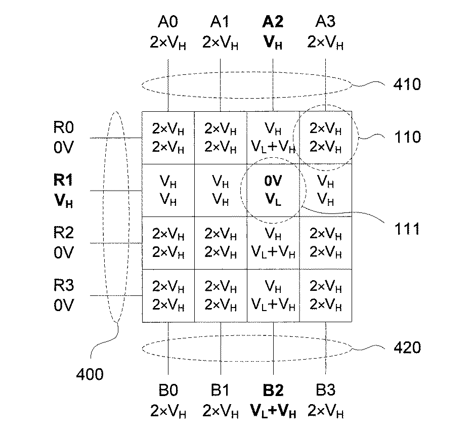
特定の実施形態によれば、図4〜図7、図10、および図24を参照して本明細書で図示および説明されるように、
● 各Rサブセットは、Nc個の移動要素を含む。
● 各Cサブセットは、Nr個の移動要素を含む。
● Rワイヤは、任意に、連続的に、または別様に、0からNr−1の番号が付けられ、それによってRワイヤの順序を定義する。本明細書で使用される番号付けは、番号が付けられる任意の要素のいかなる物理的なマーキングも含まないことを認識されたい。
● AワイヤおよびBワイヤは、任意に、連続的に、または別様に、0からNc−1の番号が付けられ、それによってAワイヤおよびBワイヤの順序を定義する。
● 移動要素には、各移動要素がNr×Cサブセット数+Rサブセット数である番号を有するように、番号が付けられる。
According to certain embodiments, as illustrated and described herein with reference to FIGS. 4-7, 10, and 24,
● Each R subset contains Nc moving elements.
• Each C subset includes Nr moving elements.
The R wires are optionally numbered sequentially or otherwise from 0 to Nr-1, thereby defining the order of the R wires. It should be appreciated that the numbering used herein does not include any physical markings of any elements that are numbered.
A wire and B wire are optionally numbered consecutively or otherwise from 0 to Nc-1, thereby defining the order of A and B wires.
• Mobile elements are numbered so that each mobile element has a number that is Nr × C subset number + R subset number.
コントローラは、各アクチュエーションクロックサイクルで、現在A位置にある全ての移動要素の番号が、連続循環シーケンスを形成し、また、現在B位置にある全ての移動要素の番号も、連続循環シーケンスを形成するように、印加−有効電位を選択し得る。 In each actuation clock cycle, the controller sets the number of all moving elements currently in the A position to form a continuous cyclic sequence, and the number of all moving elements currently in the B position also forms a continuous cyclic sequence. As such, the applied-effective potential can be selected.
特定の実施形態によれば、例えば図24を参照して本明細書で図示および説明されるように、コントローラは、k1−k2がnet_movesにより近くなる他の印加−有効電位が存在する場合を除き、各アクチュエーションクロックサイクルで、現在A位置にある全ての移動要素の番号が、単一の連続循環シーケンスを形成し、また、現在B位置にある全ての移動要素の番号も、単一の連続循環シーケンスを形成するように、印加−有効電位を選択する。任意のアクチュエーションクロックサイクルで、現在A位置にある全ての移動要素の番号および現在B位置にある全ての移動要素の番号が、それぞれ、単一の連続循環シーケンスを形成しないときに、コントローラは、以降のアクチュエーションクロックサイクルで、現在A位置にある全ての移動要素の番号が、再度単一の連続循環シーケンスを形成し、また、現在B位置にある全ての移動要素の番号も、再度単一の連続循環シーケンスを形成するように、印加−有効電位を選択し得る。任意のアクチュエーションクロックサイクルで、現在A位置にある全ての移動要素の番号および現在B位置にある全ての移動要素の番号が、それぞれ、単一の連続循環シーケンスを形成しないときに、コントローラは、k1−k2がnet_movesにより近くなる他の印加−有効電位が存在する場合を除き、以降のアクチュエーションクロックサイクルで、現在A位置にある全ての移動要素の番号が、再度単一の連続循環シーケンスを形成し、また、現在B位置にある全ての移動要素の番号も、再度単一の連続循環シーケンスを形成するように、印加−有効電位を選択し得る。 According to certain embodiments, as illustrated and described herein with reference to FIG. 24, for example, the controller may include other applied-effective potentials where k1-k2 is closer to net_moves. In each actuation clock cycle, the numbers of all moving elements currently in the A position form a single continuous cyclic sequence, and the numbers of all moving elements currently in the B position are also single consecutive The applied-effective potential is selected to form a circulation sequence. When in any actuation clock cycle, the number of all moving elements currently in the A position and the number of all moving elements currently in the B position do not form a single continuous cyclic sequence, the controller In subsequent actuation clock cycles, the number of all moving elements currently in the A position again forms a single continuous cyclic sequence, and the number of all moving elements currently in the B position is again single. The applied-effective potential can be selected to form a continuous circulation sequence of When in any actuation clock cycle, the number of all moving elements currently in the A position and the number of all moving elements currently in the B position do not form a single continuous cyclic sequence, the controller In the subsequent actuation clock cycle, all moving element numbers that are currently in the A position will again go through a single continuous cyclic sequence, unless there is another applied-effective potential where k1-k2 is closer to net_moves. The applied-effective potential can also be selected so that the numbers of all moving elements that are currently formed and also in the B position also form a single continuous circulation sequence.
特定の実施形態によれば、例えば図24を参照して本明細書で図示および説明されるように、コントローラは、各アクチュエーションクロックサイクルで、現在A位置にある全ての移動要素の番号が、Sが正の整数である、S個の連続循環シーケンスを形成し、また、現在B位置にある全ての移動要素の番号も、S個の連続循環シーケンスを形成するように、印加−有効電位を選択し得る。コントローラは、k1−k2がnet_movesにより近くなる他の印加−有効電位が存在する場合を除き、各アクチュエーションクロックサイクルで、現在A位置にある全ての移動要素の番号が、Sが正の整数である、S個の連続循環シーケンスを形成し、また、現在B位置にある全ての移動要素の番号も、S個の連続循環シーケンスを形成するように、印加−有効電位を選択し得る。任意のアクチュエーションクロックサイクルで、現在A位置にある全ての移動要素の番号および現在B位置にある全ての移動要素の番号が、それぞれ、S個を超える連続循環シーケンスを形成するときに、コントローラは、以降のアクチュエーションクロックサイクルで、現在A位置にある全ての移動要素の番号が、再度S個だけの連続循環シーケンスを形成し、また、現在B位置にある全ての移動要素の番号も、再度S個だけの連続循環シーケンスを形成するように、印加−有効電位を選択し得る。任意のアクチュエーションクロックサイクルで、現在A位置にある全ての移動要素の番号および現在B位置にある全ての移動要素の番号が、それぞれ、S個を超える連続循環シーケンスを形成するときに、コントローラは、k1−k2がnet_movesにより近くなる他の印加−有効電位が存在する場合を除き、以降のアクチュエーションクロックサイクルで、現在A位置にある全ての移動要素の番号が、再度S個だけの連続循環シーケンスを形成し、また、現在B位置にある全ての移動要素の番号も、再度S個だけの連続循環シーケンスを形成するように、印加−有効電位を選択し得る。 According to certain embodiments, as illustrated and described herein, for example, with reference to FIG. 24, the controller determines that at each actuation clock cycle, the number of all moving elements currently in the A position are: Form S continuous circulation sequences, where S is a positive integer, and the numbers of all moving elements that are currently in the B position also have applied-effective potentials so as to form S continuous circulation sequences. You can choose. In every actuation clock cycle, the number of all moving elements currently in position A is a positive integer, S, unless there is another applied-effective potential where k1-k2 is closer to net_moves. An applied-effective potential can be selected to form an S number of continuous circulation sequences, and the numbers of all moving elements currently in the B position also form an S number of continuous circulation sequences. When in any actuation clock cycle, the number of all moving elements currently in the A position and the number of all moving elements currently in the B position form a continuous cyclic sequence exceeding S, respectively. In subsequent actuation clock cycles, the numbers of all moving elements currently in position A again form only S consecutive cyclic sequences, and the numbers of all moving elements currently in position B are again The applied-effective potential can be selected to form only S continuous circulation sequences. When in any actuation clock cycle, the number of all moving elements currently in the A position and the number of all moving elements currently in the B position form a continuous cyclic sequence exceeding S, respectively. , K1-k2 is closer to net_moves, except for the case where there is another applied-effective potential, in the subsequent actuation clock cycle, the number of all moving elements currently in position A will again be S cycles continuously The applied-effective potential can be selected to form a sequence and also to form again only S continuous circulation sequences for the numbers of all moving elements currently in the B position.
特定の実施形態によれば、例えば図15〜図23を参照して本明細書で図示および説明されるように、コントローラは、任意のアクチュエーションクロックサイクル中に第1の端位置から解放される任意の移動要素の番号が、第1の端位置から直前に解放された移動要素の番号の直後に続き、Nr×Nc−1に到達した後に0に戻るように、印加−有効電位を選択する。コントローラは、k1−k2がnet_movesにより近くなる他の印加−有効電位が存在する場合を除き、任意のアクチュエーションクロックサイクル中に第1の端位置から解放される任意の移動要素の番号が、第1の端位置から直前に解放された移動要素の番号の直後に続き、Nr×Nc−1に到達した後に0に戻るように、印加−有効電位を選択し得る。コントローラは、加えて、任意のアクチュエーションクロックサイクル中に第2の端位置から解放される任意の移動要素の番号も、第2の端位置から直前に解放された移動要素の番号の直後に続き、Nr×Nc−1に到達した後に0に戻るように、印加−有効電位を選択し得る。コントローラは、加えて、k1−k2がnet_movesにより近くなる他の印加−有効電位が存在する場合を除き、任意のアクチュエーションクロックサイクル中に第2の端位置から解放される任意の移動要素の番号も、第2の端位置から直前に解放された移動要素の番号の直後に続き、Nr×Nc−1に到達した後に0に戻るように、印加−有効電位を選択し得る。コントローラは、k1−k2がnet_movesにより近くなる他の印加−有効電位が存在する場合を除き、同じアクチュエーションクロックサイクル中に第1の端位置から解放される全ての移動要素が、全て単一の第1のCサブセットの中にあるように、印加−有効電位を選択し得る。コントローラは、加えて、k1−k2がnet_movesにより近くなる他の印加−有効電位が存在する場合を除き、同じアクチュエーションクロックサイクル中に第2の端位置から解放される全ての移動要素が、全て単一の第2のCサブセットの中にあるように、印加−有効電位を選択し得る。 According to certain embodiments, the controller is released from the first end position during any actuation clock cycle, for example, as illustrated and described herein with reference to FIGS. 15-23. The applied-effective potential is selected so that the number of any moving element follows immediately after the number of the moving element released immediately before the first end position and returns to 0 after reaching Nr × Nc−1. . The controller is responsible for the number of any moving element that is released from the first end position during any actuation clock cycle, unless there is another applied-effective potential where k1-k2 is closer to net_moves. The applied-effective potential can be selected to follow immediately after the number of the mobile element released just before the end position of 1 and return to 0 after reaching Nr × Nc−1. In addition, the controller also immediately follows the number of any moving element released from the second end position during any actuation clock cycle immediately following the number of the moving element released just before the second end position. The applied-effective potential can be selected to return to 0 after reaching Nr × Nc−1. The controller additionally adds the number of any moving element that is released from the second end position during any actuation clock cycle, unless there is another applied-effective potential where k1-k2 is closer to net_moves. Alternatively, the applied-effective potential may be selected to follow immediately after the number of the mobile element released just before the second end position and return to 0 after reaching Nr × Nc−1. The controller ensures that all moving elements released from the first end position during the same actuation clock cycle are all single, unless there is another applied-effective potential where k1-k2 is closer to net_moves. The applied-effective potential may be selected to be in the first C subset. In addition, the controller will also ensure that all moving elements released from the second end position during the same actuation clock cycle are all inclusive, unless there is another applied-effective potential where k1-k2 is closer to net_moves. The applied-effective potential may be selected to be in a single second C subset.
特定の実施形態によれば、例えば図14を参照して本明細書で図示および説明されるように、コントローラは、要素選択機能とは別に、計数器、ディザーを使用する場合もあり、使用しない場合もある量子化器、少なくとも1つのレベルシフタ、低域通過フィルタ、およびサンプリングレートコンバータのうちのいくつかまたは全てを含む。 According to certain embodiments, as illustrated and described herein, for example with reference to FIG. 14, the controller may or may not use a counter, dither separately from the element selection function. It may include some or all of a quantizer, at least one level shifter, a low pass filter, and a sampling rate converter.
特定の実施形態によれば、例えば図13を参照して本明細書で図示および説明されるように、装置の電源が切られたとき等の、第1の複数のNr個の電気的接続部、第2の複数のNc個の電気的接続部、および第3の複数のNc個の電気的接続部に印加される任意の電位の非存在下で、移動要素は、第1および第2の端位置の間に位置する静止位置に戻り得、コントローラは、加えて、移動要素の1つ以上を、それらの静止位置から第1および第2の端位置まで移動させる手段を備える。コントローラは、アクチュエータアレイ内の移動要素の全てを同時に、それらの静止位置から第1および第2の端位置の1つまで移動させるように動作し得る。 According to certain embodiments, a first plurality of Nr electrical connections, such as when the device is turned off, for example as illustrated and described herein with reference to FIG. In the absence of any potential applied to the second plurality of Nc electrical connections and the third plurality of Nc electrical connections, Returning to a rest position located between the end positions, the controller additionally comprises means for moving one or more of the moving elements from their rest position to the first and second end positions. The controller may operate to move all of the moving elements in the actuator array simultaneously from their rest position to one of the first and second end positions.
コントローラは、移動要素のいくつかを、それらの静止位置から第1の端位置まで移動させる一方で、同時に、移動要素の他のものを、それらの静止位置から第2の端位置まで移動させるように動作し得る。 The controller moves some of the moving elements from their rest position to the first end position, while simultaneously moving the other of the moving elements from their rest position to the second end position. Can work.
コントローラは、単一の所定の有限集合の電位を使用して、移動要素の静止位置から第1および第2の端位置の1つまでの動き、および移動要素の第1および第2の端位置の間の動きを生じさせ得る。電位間の差は、移動要素をそれらの静止位置での平衡状態から端位置の1つまで直接移動させるのに不十分な大きさであり得る。コントローラは、所定のシーケンスの電位を、第1の複数のNr個の電気的接続部、第2の複数のNc個の電気的接続部、および第3の複数のNc個の電気的接続部の1個以上のメンバーに印加することによって、移動要素の静止位置から第1および第2の端位置までの動きを生じさせ得る。 The controller uses a single predetermined finite set of potentials to move the moving element from a stationary position to one of the first and second end positions and the first and second end positions of the moving element. Can cause movement between. The difference between the potentials may be insufficiently large to move the moving elements directly from their rest position equilibrium to one of the end positions. The controller determines a predetermined sequence of potentials of the first plurality of Nr electrical connections, the second plurality of Nc electrical connections, and the third plurality of Nc electrical connections. Application to one or more members may cause movement of the moving element from a stationary position to first and second end positions.
特定の実施形態によれば、例えば図13を参照して本明細書で図示および説明されるように、所定のシーケンスは、コントローラが、第1の複数のNr個の電気的接続部、第2の複数のNc個の電気的接続部、および第3の複数のNc個の電気的接続部のメンバーに印加される電位の1つ以上を繰り返して変化させ、よって、こうした1つ以上の電位の変化が、移動要素を、それらの機械的共振周波数でそれらの静止位置の周囲で振動させる、第1の部分と、コントローラが、第1の複数のNr個の電気的接続部、第2の複数のNc個の電気的接続部、および第3の複数のNc個の電気的接続部のメンバーに、移動させるべき端位置に向かって各移動要素を引き寄せる静電力を最大化する一組の電位を印加する、第2の部分と、を備え得る。コントローラは、移動要素のそれぞれが、反対側の端位置よりも、該移動要素を移動させるべき端位置に近い時点で、前記第1の部分から前記第2の部分への移行が起こるように動作し得る。第1の部分の間の1つ以上の電位の変化は、移動要素の機械的共振周波数の2倍である周波数で周期的に起こり得る。 According to certain embodiments, for example, as shown and described herein with reference to FIG. 13, the predetermined sequence is performed by the controller using a first plurality of Nr electrical connections, a second And repeatedly changing one or more of the potentials applied to the plurality of Nc electrical connections and the third plurality of Nc electrical connections members, so that The change causes the moving elements to vibrate around their rest position at their mechanical resonance frequency, and the controller includes a first plurality of Nr electrical connections, a second plurality Nc electrical connections, and members of the third plurality of Nc electrical connections, have a set of potentials that maximize the electrostatic force that draws each moving element toward the end position to be moved. And applying a second portion. The controller operates such that a transition from the first part to the second part occurs when each of the moving elements is closer to the end position to which the moving element is to be moved than to the opposite end position. Can do. The change in one or more potentials during the first portion can occur periodically at a frequency that is twice the mechanical resonance frequency of the moving element.
特定の実施形態によれば、例えば図27を参照して本明細書で図示および説明されるように、アドレス指定ノイズは、1つ以上のアクチュエーションクロックサイクル中にk1−k2とnet_movesとの間の非ゼロの差(アドレス指定エラー)に起因し、該アドレス指定ノイズは、周波数スペクトルを有し、コントローラは、アドレス指定ノイズの周波数スペクトルをシェーピングするように動作する、アドレス指定ノイズシェーピングループを含み、よって、アドレス指定ノイズエネルギーは、関心の周波数帯域の範囲内で低減され、かつ関心の帯域の範囲外で増大される。ノイズシェーピングループは、インパルス応答を有し、アドレス指定ノイズを受容する、ループフィルタを有し、よって、アドレス指定ノイズの周波数スペクトルが、インパルス応答によって決定されるアドレス指定ノイズ伝達関数に従ってシェーピングされ得る。 According to certain embodiments, addressing noise may be between k1-k2 and net_moves during one or more actuation clock cycles, for example as illustrated and described herein with reference to FIG. Due to a non-zero difference (addressing error), the addressing noise has a frequency spectrum, and the controller includes an addressing noise shaping pin group that operates to shape the frequency spectrum of the addressing noise. Thus, addressing noise energy is reduced within the frequency band of interest and increased outside the band of interest. The noise shaping group has an impulse response and has a loop filter that accepts addressing noise, so that the frequency spectrum of the addressing noise can be shaped according to the addressing noise transfer function determined by the impulse response.
特定の実施形態によれば、例えば図29を参照して本明細書で図示および説明されるように、量子化ノイズは、デジタル入力信号が取り得る可能な値の数よりも少ないアクチュエータアレイの中のアクチュエータ要素の数に起因し、量子化ノイズは、周波数スペクトルを有し、コントローラは、量子化ノイズの周波数スペクトルをシェーピングするように動作する、量子化ノイズシェーピングループを含み、よって、量子化ノイズエネルギーが関心の周波数帯域の範囲内で低減され、かつ関心の帯域の範囲外で増大される。ノイズシェーピングループは、インパルス応答を有し、量子化ノイズを受容するループフィルタを有し、よって、量子化ノイズの周波数スペクトルが、周波数応答によって決定される量子化ノイズ伝達関数に従ってシェーピングされ得る。 According to certain embodiments, as illustrated and described herein, for example, with reference to FIG. 29, quantization noise is less in the actuator array than the number of possible values that the digital input signal can take. Quantization noise has a frequency spectrum, and the controller includes a quantization noise shape pin group that operates to shape the frequency spectrum of the quantization noise, and thus the quantization noise. Energy is reduced within the frequency band of interest and increased outside the band of interest. The noise shape group has an impulse response and a loop filter that accepts the quantization noise, so that the frequency spectrum of the quantization noise can be shaped according to the quantization noise transfer function determined by the frequency response.
特定の実施形態によれば、例えば図28を参照して本明細書で図示および説明されるように、コントローラは、アドレス指定ノイズおよび量子化ノイズの双方の周波数スペクトルをシェーピングするように動作する、ノイズシェーピングループを含み、よって、アドレス指定ノイズエネルギーおよび量子化ノイズエネルギーがどちらも、関心の周波数帯域の範囲内で低減され、関心の帯域の範囲外で増大される。ノイズシェーピングループは、単一のインパルス応答を有し、アドレス指定ノイズおよび量子化ノイズの合計を受容する、単一のループフィルタを有し得、よって、アドレス指定ノイズおよび量子化ノイズの双方の周波数スペクトルが、単一のインパルス応答によって決定される単一のノイズ伝達関数に従ってシェーピングされる。 According to certain embodiments, the controller operates to shape the frequency spectrum of both addressing noise and quantization noise, for example, as illustrated and described herein with reference to FIG. Includes noise shaping groups, so that both addressing noise energy and quantization noise energy are reduced within the frequency band of interest and increased outside the band of interest. A noise shaping group can have a single loop filter that has a single impulse response and accepts the sum of addressing noise and quantization noise, and thus the frequency of both addressing noise and quantization noise. The spectrum is shaped according to a single noise transfer function determined by a single impulse response.
特定の実施形態によって、例えば図29を参照して本明細書で図示および説明されるように、アドレス指定ノイズは、1つ以上のアクチュエーションクロックサイクル中にk1−k2とnet_movesとの間の非ゼロの差(アドレス指定エラー)に起因し、アドレス指定ノイズは、アドレス指定ノイズスペクトルを有し、本装置はまた、デジタル入力信号が取り得る可能な値の数よりも少ないアクチュエータアレイの中のアクチュエータ要素の数に起因する、量子化ノイズも受け、量子化ノイズは、量子化ノイズスペクトルを有し、コントローラは、アドレス指定ノイズの周波数スペクトルをシェーピングするように動作する、アドレス指定ノイズシェーピングループと、量子化ノイズの周波数スペクトルをシェーピングするように動作する、量子化ノイズシェーピングループとを含み、よって、アドレス指定ノイズエネルギーおよび量子化ノイズエネルギーがどちらも、それぞれの関心の周波数帯域の範囲内で低減され、関心の帯域の範囲外で増大される。アドレス指定ノイズシェーピングループは、第1のインパルス応答を有し、アドレス指定ノイズを受容する、第1のループフィルタを有し得、量子化ノイズシェーピングループは、第2のインパルス応答を有し、量子化ノイズを受容する、第2のループフィルタを有し得、よって、アドレス指定ノイズの周波数スペクトルが、第1のインパルス応答によって決定される第1のノイズ伝達関数に従ってシェーピングされ、量子化ノイズの周波数スペクトルが、第2のインパルス応答によって決定される第2のノイズ伝達関数に従ってシェーピングされる。 Depending on the particular embodiment, as illustrated and described herein, for example, with reference to FIG. 29, addressing noise is a non-between k1-k2 and net_moves during one or more actuation clock cycles. Due to the zero difference (addressing error), the addressing noise has an addressing noise spectrum, and the device also includes fewer actuators in the actuator array than the number of possible values that the digital input signal can take. Due to the number of elements, the quantization noise is also received, the quantization noise has a quantization noise spectrum, and the controller operates to shape the frequency spectrum of the addressing noise, and an addressing noise shaping pin group; Works to shape the frequency spectrum of quantization noise That, and a quantization noise shaping loop, therefore, both addressing the noise energy and quantization noise energy, is reduced within the frequency band of the respective interest is increased by the outside of the band of the interest. The addressed noise shape group may have a first loop filter that has a first impulse response and accepts addressing noise, the quantized noise shape group has a second impulse response, The frequency spectrum of the addressing noise is shaped according to a first noise transfer function determined by the first impulse response and the frequency of the quantization noise The spectrum is shaped according to a second noise transfer function determined by the second impulse response.
特定の実施形態によれば、例えば図13を参照して本明細書で図示および説明されるように、第2の部分の持続期間は、移動要素の機械的共振周期(Tres)の少なくとも半分である。一組の電位は、所定の有限集合の電位から選択され得、第2の部分の間、変化しない。 According to certain embodiments, the duration of the second portion is at least half the mechanical resonance period (Tres) of the moving element, as shown and described herein, for example with reference to FIG. is there. The set of potentials can be selected from a predetermined finite set of potentials and do not change during the second portion.
特定の実施形態によれば、例えば図24を参照して本明細書で図示および説明されるように、コントローラは、各アクチュエーションクロックサイクルで、
RワイヤR0〜R(Nr−1)のそれぞれに印加される電位を制御する、Nr個のR信号r0〜r(Nr−1)、
AワイヤA0〜A(Nc−1)のそれぞれに印加される電位を制御する、Nc個のA信号a0〜a(Nc−1)、および
BワイヤB0〜B(Nc−1)のそれぞれに印加される電位を制御する、Nc個のB信号b0〜b(Nc−1)、を生成する。
According to certain embodiments, as illustrated and described herein, for example, with reference to FIG.
Nr R signals r0 to r (Nr-1) for controlling the potential applied to each of the R wires R0 to R (Nr-1),
Controls the potential applied to each of the A wires A0 to A (Nc-1), and applies to each of the Nc A signals a0 to a (Nc-1) and B wires B0 to B (Nc-1) Nc B signals b0 to b (Nc-1) for controlling the potential to be generated are generated.
Rワイヤに対するR信号の割り当て、Aワイヤに対するA信号の割り当て、およびBワイヤに対するB信号の割り当ては固定され得、よって、例えば、
R信号r0〜r(Nr−1)のそれぞれが、常時同じRワイヤを制御し、
A信号a0〜a(Nc−1)のそれぞれが、常時同じAワイヤを制御し、
B信号b0〜b(Nc−1)のそれぞれが、常時同じBワイヤを制御する。
The assignment of the R signal to the R wire, the assignment of the A signal to the A wire, and the assignment of the B signal to the B wire can be fixed, for example,
Each of the R signals r0-r (Nr-1) always controls the same R wire,
Each of the A signals a0 to a (Nc-1) always controls the same A wire,
Each of the B signals b0 to b (Nc-1) always controls the same B wire.
随意に、コントローラは、装置の動作中に、Rワイヤに対するR信号の割り当て、ならびに/またはAワイヤに対するA信号の割り当て、およびBワイヤに対するB信号の割り当てを変化させる。 Optionally, the controller changes the R signal assignment to the R wire and / or the A signal assignment to the A wire and the B signal assignment to the B wire during operation of the device.
Rワイヤに対するR信号の割り当て、ならびに/またはAワイヤに対するA信号の割り当て、およびBワイヤに対するB信号の割り当てにおける変化は、周期的に起こり得る。 Changes in the assignment of the R signal to the R wire and / or the assignment of the A signal to the A wire and the assignment of the B signal to the B wire can occur periodically.
Rワイヤに対するR信号の割り当て、ならびに/またはAワイヤに対するA信号の割り当て、およびBワイヤに対するB信号の割り当てにおける変化は、アクチュエーションクロックと同期的に起こり得る。 Changes in the assignment of the R signal to the R wire and / or the assignment of the A signal to the A wire and the assignment of the B signal to the B wire can occur synchronously with the actuation clock.
Rワイヤに対するR信号の割り当て、ならびに/またはAワイヤに対するA信号の割り当て、およびBワイヤに対するB信号の割り当てにおける変化は、その後に移動要素が端位置の1つから解放される順序を変更し得る。 Changes in the assignment of the R signal to the R wire and / or the assignment of the A signal to the A wire and the assignment of the B signal to the B wire can subsequently change the order in which the moving elements are released from one of the end positions. .
Rワイヤに対するR信号の割り当て、ならびに/またはAワイヤに対するA信号の割り当て、およびBワイヤに対するB信号の割り当てにおける変化は、各アクチュエータ要素によって生成される物理的作用の大きさの差に起因する不整合ノイズの周波数スペクトルをシェーピングし得、よって、装置によって生成される物理的作用が、全体として、標的の物理的作用に密に類似する。不整合ノイズの周波数スペクトルをシェーピングすることは、例えば、不整合ノイズの周波数スペクトルのピークの大きさを低減することを含み得る。 Changes in the assignment of the R signal to the R wire and / or the assignment of the A signal to the A wire and the assignment of the B signal to the B wire are due to differences in the magnitude of the physical action produced by each actuator element. The frequency spectrum of the matched noise can be shaped so that the physical action generated by the device is generally closely similar to the target physical action. Shaping the frequency spectrum of the mismatched noise may include, for example, reducing the magnitude of the peak of the frequency spectrum of the mismatched noise.
典型的に、Rワイヤに対するR信号の割り当て、ならびに/またはAワイヤに対するA信号の割り当て、およびBワイヤに対するB信号の割り当てにおける変化は、Rワイヤ、Aワイヤ、およびBワイヤに印加されるいかなる電位のいかなる即時の変化ももたらさない。 Typically, a change in the assignment of the R signal to the R wire and / or the assignment of the A signal to the A wire and the assignment of the B signal to the B wire will result in any potential applied to the R wire, A wire, and B wire. Does not bring any immediate changes in
典型的に、Rワイヤに対するR信号の割り当て、ならびに/またはAワイヤに対するA信号の割り当て、およびBワイヤに対するB信号の割り当てにおける変化は、アクチュエータアレイ内の任意の移動要素の位置のいかなる即時の変化ももたらさない。 Typically, a change in the assignment of the R signal to the R wire and / or the assignment of the A signal to the A wire and the assignment of the B signal to the B wire will result in any immediate change in the position of any moving element in the actuator array. Also does not bring.
「即時の」という用語は、Rワイヤに対するR信号の割り当て、ならびに/またはAワイヤに対するA信号の割り当て、およびBワイヤに対するB信号の割り当てにおける変化が実質的に同時に起こることを指す。 The term “immediately” refers to the fact that changes in the assignment of the R signal to the R wire and / or the assignment of the A signal to the A wire and the assignment of the B signal to the B wire occur substantially simultaneously.
Rワイヤに対するR信号の割り当てにおける変化は、2つのR信号を交換することを含み得る、よって、第1のR信号によって以前に制御された第1のRワイヤが、第2のR信号によって制御されるようになり、第2のR信号によって以前に制御された第2のRワイヤが、第1のR信号によって制御されるようになる。 Changes in the assignment of R signals to R wires can include exchanging two R signals, so that a first R wire previously controlled by a first R signal is controlled by a second R signal. And the second R wire previously controlled by the second R signal is controlled by the first R signal.
コントローラは、複数組の交換可能なR信号を識別し、複数組の交換可能なR信号の少なくとも1つが2つ以上のメンバーを有する場合に、Rワイヤに対するR信号の新しい割り当てを決定するように動作し得る。 The controller identifies the plurality of sets of exchangeable R signals and determines a new assignment of R signals to the R wires when at least one of the plurality of exchangeable R signals has two or more members. Can work.
コントローラは、複数組の交換可能なR信号を識別するように動作し、よって、1組の交換可能なR信号の中の任意の特定のR信号について、そのRワイヤが特定のR信号によって現在制御されている、Rサブセットの中の移動要素、およびそのRワイヤが同じ組の交換可能なR信号の中の別のR信号によって現在制御されている全てのRサブセット中の移動要素が、全て同じ位置にあり、かつ(運動中であれば)同じ方向に移動している。 The controller operates to identify multiple sets of exchangeable R signals, so that for any particular R signal in a set of exchangeable R signals, the R wire is currently represented by a particular R signal. The moving elements in the R subset that are being controlled, and the moving elements in all R subsets whose R wires are currently controlled by another R signal in the same set of interchangeable R signals, are all They are in the same position and are moving in the same direction (if in motion).
コントローラは、複数組の交換可能なR信号を識別するように動作し、よって、1組の交換可能なR信号の中の任意の特定のR信号について、および0からNc−1まで(Nc−1を含む)の任意の番号iについて、Cサブセットiと、そのRワイヤが特定のR信号によって現在制御されているRサブセットとの交差点にある移動要素は、Cサブセットiと、そのRワイヤが同じ組の交換可能なR信号の中の任意の他のR信号によって現在制御されている任意の他のRサブセットとの交差点にある移動要素と同じ位置にあり、かつ(運動中であれば)同じ方向に移動している。 The controller operates to identify multiple sets of exchangeable R signals, thus for any particular R signal in the set of exchangeable R signals and from 0 to Nc−1 (Nc− For any number i (including 1), the moving element at the intersection of C subset i and the R subset whose R wire is currently controlled by a particular R signal is C subset i and its R wire is In the same position as the moving element at the intersection with any other R subset currently controlled by any other R signal in the same set of interchangeable R signals, and (if in motion) They are moving in the same direction.
コントローラは、Rワイヤに対するR信号の新しい割り当てを決定するために、疑似乱数発生器を用い得る。 The controller may use a pseudo random number generator to determine a new assignment of R signals to the R wires.
Aワイヤに対するA信号の割り当ておよびBワイヤに対するB信号の割り当てにおける変化は、2つのA信号およびそれぞれのB信号を交換することを含み得、よって、例えば、第1のA信号および第1のB信号によって、それぞれ、以前に制御された第1のAワイヤおよび第1のBワイヤが、第2のA信号および第2のB信号によって、それぞれ、制御されるようになり、第2のA信号および第2のB信号によって、それぞれ、以前に制御された第2のAワイヤおよび第2のBワイヤが、第1のA信号および第1のB信号によって、それぞれ、制御されるようになる。 Changes in the assignment of the A signal to the A wire and the assignment of the B signal to the B wire can include exchanging the two A signals and the respective B signals, for example, the first A signal and the first B signal. The signal causes the previously controlled first A wire and first B wire to be controlled by the second A signal and the second B signal, respectively, and the second A signal. And the second B signal, respectively, the previously controlled second A wire and second B wire are controlled by the first A signal and the first B signal, respectively.
コントローラは、複数組の交換可能なA信号およびそれぞれのB信号を識別するように動作し得、複数組の交換可能なA信号の少なくとも1つおよびそれぞれのB信号は、Aワイヤに対するA信号の新しい割り当て、およびBワイヤに対するそれぞれのB信号の新しい割り当てを決定するために、2つ以上のメンバーを有する。 The controller may be operative to identify multiple sets of exchangeable A signals and respective B signals, wherein at least one of the multiple sets of exchangeable A signals and each B signal may be an A signal for an A wire. It has two or more members to determine a new assignment and a new assignment of each B signal to the B wire.
コントローラは、複数組の交換可能なA信号およびそれぞれのB信号を識別するように動作し、よって、1組の交換可能なA信号およびそれぞれのB信号の中の任意の特定のA信号および特定のB信号について、そのAワイヤおよびBワイヤが、それぞれ、特定のA信号および特定のB信号によって現在制御されている、Cサブセットの中の移動要素、およびそのAワイヤおよびBワイヤが同じ組の交換可能なA信号およびそれぞれのB信号の中の別のA信号およびそのそれぞれのBワイヤによって現在制御されている、全てのCサブセットの中の移動要素が、全て同じ位置にあり、かつ(運動中であれば)同じ方向に移動している。 The controller operates to identify multiple sets of interchangeable A signals and respective B signals, and thus any specific A signal and specific within a set of interchangeable A signals and each B signal. For a B signal, the A wire and the B wire are currently controlled by a specific A signal and a specific B signal, respectively, and the moving element in the C subset and the A wire and the B wire are in the same set The moving elements in all C subsets currently controlled by the exchangeable A signal and another A signal in each B signal and its respective B wire are all in the same position and It ’s moving in the same direction.
コントローラは、複数組の交換可能なA信号およびそれぞれのB信号を識別するように動作し、よって、1組の交換可能なA信号およびそれぞれのB信号の中の任意の特定のA信号および特定のB信号について、および0からNr−1まで(Nr−1を含む)の任意の番号iについて、Rサブセットiと、そのAワイヤおよびBワイヤが特定のA信号および特定のB信号によって、それぞれ、現在制御されている、Cサブセットとの交差点にある移動要素は、Rサブセットiと、そのAワイヤおよびBワイヤが同じ組の交換可能なA信号およびそれぞれのB信号の中のA信号およびそのそれぞれのB信号の1つによって現在制御されている、任意の他のCサブセットとの交差点にある移動要素と同じ位置にあり、かつ(運動中であれば)同じ方向に移動している。 The controller operates to identify multiple sets of interchangeable A signals and respective B signals, and thus any specific A signal and specific within a set of interchangeable A signals and each B signal. And for any number i from 0 to Nr-1 (including Nr-1), the R subset i and its A and B wires are defined by a specific A signal and a specific B signal, respectively. The currently controlled moving element at the intersection with the C subset is the R subset i and its A and B wires in the same set of interchangeable A signals and the A signal in each B signal and its In the same position as the moving element at the intersection with any other C subset currently controlled by one of the respective B signals, and the same (if in motion) It is moving in the direction.
コントローラは、Aワイヤに対するA信号の新しい割り当て、およびBワイヤに対するそれぞれのB信号の新しい割り当てを決定するために、疑似乱数発生器を用いる。 The controller uses a pseudo-random number generator to determine a new assignment of A signals to A wires and a new assignment of each B signal to B wires.
コントローラは、複数組の交換可能なR信号を識別するように動作し得、よって、1組の交換可能なR信号の中の各特定のR信号について、該特定のR信号によって制御されるRワイヤに現在印加されている電位は、同じ組の交換可能なR信号の中の任意の他のR信号によって制御される任意のRワイヤに現在印加されている電位と同じである。 The controller may operate to identify multiple sets of exchangeable R signals, so for each particular R signal in the set of exchangeable R signals, the R controlled by the particular R signal. The potential currently applied to the wire is the same as the potential currently applied to any R wire controlled by any other R signal in the same set of interchangeable R signals.
コントローラは、複数組の交換可能なA信号およびそれぞれのB信号を識別するように動作し得、よって、一組の交換可能なA信号およびそれぞれのB信号の中の特定のA信号およびそれぞれのB信号について、該特定のA信号およびそれぞれのB信号によって制御されるAワイヤおよびそれぞれのBワイヤに現在印加されている電位は、同じ組の交換可能なA信号およびそれぞれのB信号の中の任意の他のA信号およびそれぞれのB信号によって制御される任意のAワイヤおよびそれぞれのBワイヤに現在印加されている電位と同じである。 The controller may operate to identify a plurality of sets of exchangeable A signals and respective B signals, and thus a set of exchangeable A signals and specific A signals within each B signal and each For a B signal, the A wire controlled by that particular A signal and the respective B signal and the potential currently applied to each B wire is the same as the set of interchangeable A signals and each B signal. It is the same as the potential currently applied to any A wire and each B wire controlled by any other A signal and each B signal.
「現在」という用語は、以下の時点での発生を含むことを意図する:
● コントローラが、交換可能な組の「識別」を行った、または
● コントローラが、交換可能な組の「識別」を行った、アクチュエーションクロックサイクル中、または
● 現在のアクチュエーションクロックサイクル中
The term “current” is intended to include occurrences at the following times:
● The controller has “identified” a replaceable pair, or ● The controller has “identified” a replaceable pair, during an actuation clock cycle, or ● During the current actuation clock cycle
ここで、本発明を適用することができる両面静電アクチュエータ要素の1つのタイプの断面図である、図1A〜1Cを参照する。アクチュエータ要素は、フレキシャまたはばね等の好適なベアリング150によってアクチュエータ要素の固定部に機械的に接続される、移動要素120を含む。ベアリング150は、移動要素120がそれに沿って進行することができる軸125を画定し、移動要素120が別の方向に進行することを防止し、また、移動要素120の静止位置を画定する。アクチュエータ要素はさらに、移動要素120の両側に配置される、2つの電極130および140を備え、以下、それぞれ、「A電極」および「B電極」と称する。移動要素120は、スペーサ180および190によって、電極130および140から分離される。ディンプル210および220は、それぞれ、電極130および140の表面に形成され、移動要素120に対面する。
Reference is now made to FIGS. 1A-1C, which are cross-sectional views of one type of double-sided electrostatic actuator element to which the present invention can be applied. The actuator element includes a moving
図1Aは、移動要素120と電極130および140のどちらとの間にも、いかなる電圧も印加されていない状態で、その静止位置にある移動要素120を示す。
FIG. 1A shows the moving
移動要素とどちらかの電極との間に電圧を印加すると、移動要素をその電極に向かって引き寄せる静電力が生成され、この静電力の大きさは、印加される電圧の大きさに比例し、かつ移動要素120とそれぞれの電極との対向面間の分離距離の2乗に反比例する。同時に、その静止位置から離れる移動要素120の任意の動きは、ベアリング150に、移動要素120をその静止位置に向かって引き戻すばね力を該移動要素に働かせる。移動要素120はまた、長期間にわたる信頼性を改善するため等の実用的な理由から、自然に起こり得るか、または意図的に導入され得る、減衰力または摩擦力等の、他の力による影響も受け得る。しかしながら、そのようなさらなる力は、本発明の目的には必要とされない。移動要素120は、それに作用する全ての力の合計がゼロである平衡位置に到達し得るか、または図1Bおよび1Cを参照して説明されるようにラッチされ得る。
Applying a voltage between the moving element and either electrode generates an electrostatic force that pulls the moving element toward that electrode, the magnitude of this electrostatic force being proportional to the magnitude of the applied voltage, And it is in inverse proportion to the square of the separation distance between the opposing surfaces of the moving
図1Bは、A電極130にできるだけ近く、かつB電極140からできるだけ離れた、以下「A位置」とも称される、第1の端位置にラッチされた移動要素120を示す。典型的に、移動要素120は、電圧VAがA電極130と移動要素120との間に印加され、移動要素120をA電極130に向かって引き寄せる、以下「A力」とも称される静電力を発生させた結果として、この位置に到達する。移動要素120がA電極130に接近するにつれて、A力は、移動要素120と電極130との対向面間の分離距離の2乗に反比例して増大するが、移動要素120をその静止位置に向かって引き戻すばね力は、その静止位置からの該移動要素の偏差に比例して増大する。ベアリング150のばね定数、およびVAの範囲に応じて、A力およびばね力が等しい軸125に沿って臨界点が存在し得、移動要素120のA電極130に向かう任意のさらなる進行は、ばね力よりも迅速にA力を増大させる。移動要素120がこの臨界点を僅かでも超えて移動し、VAが一定のままであると仮定した場合、移動要素120がディンプル210と接触するまで、力の平衡が、該移動要素をA電極130に向かって加速させる。このプロセスは、以下「ラッチング」と称される。ラッチングの後、移動要素120をこの位置に保持するのに十分なVAの大きさ(以下、「保持電圧」と称される)は、移動要素120のA位置へのラッチングを達成するのに十分なVAの大きさ(以下、「ラッチング電圧」と称される)よりも小さい。
FIG. 1B shows the moving
移動要素120がA位置でラッチされ、第2の電圧VBがB電極140と移動要素120との間に印加されたとき、VBに起因する静電力は、等しい大きさのVAに起因するA力よりも大きさがはるかに小さい。したがって、非ゼロVBの存在は、移動要素120をA位置にラッチし続けるのに十分な保持電圧の大きさを僅かだけしか増大させない。
When the moving
その後、VAが保持電圧よりも低くなると、A力の大きさがばね力よりも小さくなり、移動要素120を、A位置からその静止位置に向かって移動させる。このプロセスは、以下「解放」と称される。VAおよびVBがどちらもゼロに等しくなると、移動要素120は、その振動の周波数で、その静止位置の周辺で振動する。該周波数は、以下該移動要素の「機械的共振周波数」とも称され、主に、移動要素120の質量およびベアリング150(減衰を無視する)のばね定数によって決定され、振動の振幅は、摩擦、空気減衰、または他のエネルギー損失のため、徐々に減少する。代替として、十分な大きさの非ゼロVBの存在下で、移動要素120は、B電極140にできるだけ近く、A電極130からできるだけ離れた、以下「B位置」とも称される、第2の端位置にラッチされる。
Thereafter, when VA becomes lower than the holding voltage, the magnitude of the A force becomes smaller than the spring force, and the moving
本発明の一実施形態によれば、コントローラは、移動要素120が常時A位置もしくはB位置のいずれかにあるように、またはこれらの2つの位置の間を移行するようにVAおよびVBを調整し得る。すなわち、通常動作中に、移動要素120は、2つの端位置を除いて、その静止位置または任意の他の位置に決して定着しない。
According to one embodiment of the present invention, the controller sets V A and V B so that the moving
2つの端位置間での移行中に、移動要素120がその静止位置に到達したときに、該移動要素は、電極130および140に対する非ゼロ運動エネルギーおよび直線速度を有し、したがって、その運動エネルギーがベアリング150によって吸収されるまで、その新しい端位置に向かって進行し続ける。その新しい端位置により近い位置から移動要素120をラッチするには、移動要素120をその静止位置の平衡状態からその同じ端位置にラッチするよりも小さい静電力を必要とするので、端位置間の移行のためのラッチ電圧は、静止位置からラッチするためのラッチ電圧よりも低い。
During the transition between the two end positions, when the moving
ディンプル210の目的は、空隙240を維持することであり、それによって、空隙を伴わない場合よりも容易に、空気が電極130の中の穴270を通って、移動要素120と第1の電極130との間の空間の中に流れることを可能にし、それによって、A位置からの移動要素120のより速い解放を容易にする。ディンプル210が電気的絶縁材料を含む場合、それらは、電極130から移動要素120を絶縁する役割も果たす。ディンプル210が導電性材料を含む場合、移動要素120および電極130の少なくとも1つを電気的絶縁材料で被覆する等の、電気的絶縁のいくつかの他の手段が用いられ得る。
The purpose of the
図1Cは、電極140にできるだけ近く、電極130からできるだけ離れてB位置でラッチされた、移動要素120を示す。移動要素120のB位置へのラッチングおよびB位置からの解放は、図1Bを参照して上で説明したものと類似した様式で達成され、A電極130およびB電極140の役割、VAおよびVBの役割、およびA力およびB力の役割が逆になる。ディンプル220および空隙250の機能は、上で説明したディンプル210および空隙240の機能に類似している。特定の実施形態において、アクチュエータ要素の幾何学形状は、移動要素120の平面に関して実質的に対称的であり、A位置に対するものと実質的に等しい、B位置に対する保持電圧およびラッチング電圧をもたらす。代替として、アクチュエータ要素の幾何学形状は、非対称的であってもよい。例えば、スペーサ180および190は、厚さが異なってもよく、その結果、A位置およびB位置について、それぞれ、2つの異なるラッチング電圧がもたらされ、および/またはディンプル210および220は、高さが異なってもよく、その結果、2つの異なる保持電圧がもたらされる。
FIG. 1C shows the moving
図1A〜1Cで示されるようなアクチュエータ要素を製作するための好適な材料および製造技術、ならびに密接に関連したタイプのアクチュエータ要素は、2011年9月15日に公開された共同所有の国際公開第WO2011/111042号(「Electrostatic Parallel Plate Actuators Whose Moving Elements Are Driven Only By Electrostatic Force and Methods Useful in Conjunction Therewith」)で論じられている。 Suitable materials and manufacturing techniques for fabricating actuator elements as shown in FIGS. 1A-1C, as well as closely related types of actuator elements, are disclosed in commonly owned International Publication No. 15/2011. WO2011-111042 ("Electrostatic Parallel Plate Actuators Who Moving Elements Are Driven Only By Electrostatic Force and Methods Usefulness in Confluence").
本発明は、いかなる特定の材料または製造技術にも依存しない。 The present invention does not depend on any particular material or manufacturing technique.
電圧VAおよびVBの極性は、これらの電圧の極性に関わらず、どちらの静電力も同じであるので、アクチュエータ要素の動作に影響を及ぼすことなく、逆にすることができることを認識されたい。 It should be appreciated that the polarities of voltages V A and V B can be reversed without affecting the operation of the actuator element, since both electrostatic forces are the same regardless of the polarity of these voltages. .
本明細書で図示および説明されるデバイスの水平に対する配向は、示されるようなものである必要はない。例えば、図1A〜1Cの装置は、示されるように層が水平であるように配置されてもよく、または例えば、層が垂直であるように配置されてもよい。また、装置は、横倒しにセットしてもよく、または、所望であれば、逆さにするのではなく、移動要素120が電極層140の最上部にあるように、反転させてもよい。特定の実施形態によれば、ベアリング150によって移動要素に及ぼされる力、および電極(単数または複数)によって発生する静電力は、重力より何桁も大きいので、重力は、無視することができる。
The horizontal orientation of the devices shown and described herein need not be as shown. For example, the devices of FIGS. 1A-1C may be arranged such that the layers are horizontal as shown, or may be arranged, for example, such that the layers are vertical. Also, the device may be set on its side or inverted if desired so that the moving
本発明の装置は、通常、空気中で動作するが、そうとは限らず、代替として、例えば、該装置は、任意の他の好適な媒体中で動作し得るので、「空隙」という用語は、単に一例として使用される。 The device of the present invention usually operates in air, but this is not always the case, and alternatively, for example, the term “air gap” is used because the device can operate in any other suitable medium. , Just used as an example.
図1A〜1Cで示されるディンプルは本発明の目的には必要とされないことも認識されたい。さらに、ディンプルは、電極210および220の代わりに移動要素120の表面に形成することができ、または例えば2011年9月15日に公開された共同所有の国際公開第WO2011/111042号(「Electrostatic Parallel Plate Actuators Whose Moving Elements Are Driven Only By Electrostatic Force and Methods Useful in Conjunction Therewith」)の図2で表されるような機械的リミッタがディンプルの代わりに使用され得る。
It should also be appreciated that the dimples shown in FIGS. 1A-1C are not required for the purposes of the present invention. Further, the dimples can be formed on the surface of the moving
図2は、例えば、複数の静電アクチュエータ要素110を備える、本発明の特定の実施形態に従うアクチュエータアレイの模式図であり、例えば、図1A〜1Cを参照して本明細書で図示および説明されるタイプであり得る。
FIG. 2 is a schematic diagram of an actuator array, eg, comprising a plurality of
アクチュエータ要素110は、以下「Rサブセット」と称され、その移動要素が電気的に相互接続される、Nr個の第1のサブセットにパーティショニングされ、その結果、以下「Rワイヤ」と称される、1組のNr個の相互接続部400をもたらす。加えて、アクチュエータ要素110はまた、以下「Cサブセット」と称され、そのA電極およびB電極が、それぞれ、電気的に相互接続される、Nc個の第2のサブセットにもパーティショニングされ、その結果、以下「Aワイヤ」と称される、A電極のための第1の1組のNc個の相互接続部410、および以下「Bワイヤ」と称される、A電極のための第2の1組のNc個の相互接続部420をもたらす。
図ではNrもNcも3個であるが、サブセットは、任意の数のアクチュエータ要素を含み得る。特定の実施形態において、全てのRサブセットは、Nc個のアクチュエータ要素を含み、全てのCサブセットは、Nr個のアクチュエータ要素を含み、そしてアレイ移動要素の総数は、Nr×Nc個である。図2において、Rサブセットは、横列で配設され、Cサブセットは、縦列で配設されているが、アクチュエータ要素の任意の他のレイアウトも使用され得る。 Although Nr and Nc are three in the figure, the subset may include any number of actuator elements. In a particular embodiment, all R subsets include Nc actuator elements, all C subsets include Nr actuator elements, and the total number of array moving elements is Nr × Nc. In FIG. 2, the R subset is arranged in rows and the C subset is arranged in columns, but any other layout of actuator elements may be used.
各Rワイヤ、Aワイヤ、およびBワイヤは、コントローラ50にも接続される。したがって、アレイとコントローラ50との間の電気的相互接続部の総数はNr+2Ncであるが、各アクチュエータ要素のための専用の相互接続部による実装は、より多くのそのような相互接続部を用い得る。例えば、各移動要素について別々の相互接続部を提供すると、各A電極および各B電極は、3×Nr×Nc個の相互接続部を用い得る。代替として、例えば2011年9月15日に公開された共同所有の国際公開第WO2011/111042号(「Electrostatic Parallel Plate Actuators Whose Moving Elements Are Driven Only By Electrostatic Force and Methods Useful in Conjunction Therewith」)で説明されているように、各移動要素のための別々の相互接続部に、全てのA電極および全てのB電極のそれぞれについて1つの共有接続部を加えて提供することで、(Nr×Nc)+2個の相互接続部を用い得る。
Each R wire, A wire, and B wire are also connected to the
説明されているタイプのアクチュエータアレイは、例えば2011年9月15日に公開された共同所有の国際公開第WO2011/111042号(「Electrostatic Parallel Plate Actuators Whose Moving Elements Are Driven Only By Electrostatic Force and Methods Useful in Conjunction Therewith」)で説明されているようなMEMS製作技術を使用して、例えば、シリコンもしくは他の半導体の単一のモノリシックダイ上に、または特定の金属上に製造され得る。 An actuator array of the type described is described, for example, in co-owned international publication WO 2011/1111042 published on September 15, 2011 (“Electrostatic Parallel Plate Actuators Who Driving in the United States of America”). It can be fabricated, for example, on a single monolithic die of silicon or other semiconductor, or on a specific metal, using MEMS fabrication techniques such as those described in “Conjunction Thewith”).
図3は、本発明の特定の実施形態に従うアクチュエータアレイの模式図であり、図2に示されるアレイに類似しているが、Rサブセットは、横列と一致しておらず、また、Cサブセットは、縦列と一致していない。アレイは、64個のアクチュエータ要素110を備え、8つのRサブセットおよび4つのCサブセットにパーティショニングされている。各Rサブセットは、それぞれ、R0からR7にラベル付けされた、1個のRワイヤを有し、各Cサブセットは、それぞれ、A0からA3およびB0からB3にラベル付けされた、1個のAワイヤおよび1個のBワイヤ有する。1個のRサブセットおよび1個のCサブセットの交差点毎に、2個のアクチュエータ要素を含む。Rサブセット毎に、1つの横列からの4つのアクチュエータ要素、および別の横列からの4個のアクチュエータ要素を含む。例えば、RワイヤR1と関連付けられるRサブセット1は、先頭の横列の左側半分、および先頭からの2番目の横列の右側半分を含む。Cサブセット毎に、2個の隣接する縦列の全てのアクチュエータ要素を含む。例えば、AワイヤA1およびBワイヤB1と関連付けられるCサブセット1は、左から3番目および4番目の縦列を含む。
FIG. 3 is a schematic diagram of an actuator array according to a particular embodiment of the present invention, similar to the array shown in FIG. 2, but the R subset does not coincide with the row and the C subset is , Does not match the column. The array comprises 64
本発明に従って構成されるアクチュエータアレイは、任意のパターンでレイアウトされるそれらのアクチュエータ要素を有し得、また、1個のRサブセットおよび1個のCサブセットの各交差点で、任意の数のアクチュエータ要素を有し得る。特定の実施形態は、各当該交差点で同じ数のアクチュエータ要素を有する。 An actuator array constructed in accordance with the present invention may have those actuator elements laid out in any pattern, and any number of actuator elements at each intersection of one R subset and one C subset. Can have. Certain embodiments have the same number of actuator elements at each such intersection.
単一の、特定のアクチュエータ要素の「ラッチング電圧」および「保持電圧」という用語は、上で図1Bを参照して定義した。以下、これらの用語は、そのアクチュエータ要素の全てが全く同一でなくてもよい、アクチュエータアレイについて定義される。加えて、「解放電圧」という用語も、下で使用するために定義される。
● 「ラッチング電圧」VLとは、移動要素が対向する端位置から解放された後に、図1Bを参照して説明したそのA位置またはB位置のどちらかに、アレイ内の移動要素のいずれも確実にラッチするのにちょうど十分な大きさの電圧を意味する。このアクチュエータアレイのためのラッチング電圧は、典型的に、図1Bを参照して上で定義した個々のアクチュエータ要素のためのラッチング電圧よりも僅かに高いが、その理由は、例えば以下の通りである。(1)個々のアクチュエータ要素の幾何学形状が製造許容差により変動し得るので、各個々のアクチュエータ要素が、僅かに異なるラッチング電圧を有し得る。ここで定義されるVLは、典型的に、定義上はそれらの全てを超える。(2)同様に、アクチュエータ要素の幾何学形状における非対称性が、そのA位置およびB位置について、それぞれ、2つの異なるラッチング電圧を生成し得る。この場合には、典型的に、ここで定義されるVLは、2つのうちの高い方を超える。(3)アクチュエータアレイの意図された使用に依存して、アクチュエータ要素110が、それらの移動要素120に対するさらなる力を生成し得る環境条件、例えば、機械的な衝撃(例えば、携帯/手持ち型用途の場合)、磁界、または気流にさらされる。ラッチングを信頼できるものとするために、ここで定義されるVLは、典型的に、アレイが設計された環境条件下で、そのようなさらなる力に打ち勝つのに十分である。
● 「保持電圧」VHとは、2つの端位置のどちらかに、アレイ内の移動要素のいずれも保持するのにちょうど十分な大きさの電圧を意味する。この保持電圧は、典型的に、「ラッチング電圧」に関して上で説明したものと同じ理由で、図1Bを参照して定義した個々のアクチュエータ要素のための保持電圧よりも僅かに高くなる。
● 「解放電圧」VRとは、その大きさが、アレイ内のアクチュエータ要素のいずれも、その2つの端位置のどちらかから解放するのにちょうど十分に低い電圧を意味する。理想的なアクチュエータ要素に関して、VRとVHとの間の差は、極小である。しかしながら、実際のアレイでは、「ラッチング電圧」に関して上で説明した製造許容差、非対称性、および環境条件のため、VRとVHとの間に有限の差がある。
The terms “latching voltage” and “holding voltage” for a single, specific actuator element were defined above with reference to FIG. 1B. In the following, these terms are defined for an actuator array in which not all of the actuator elements may be identical. In addition, the term “release voltage” is also defined for use below.
● “Latching voltage” V L means that any of the moving elements in the array is in either the A or B position described with reference to FIG. 1B after the moving element is released from the opposite end position. It means a voltage just large enough to reliably latch. The latching voltage for this actuator array is typically slightly higher than the latching voltage for the individual actuator elements defined above with reference to FIG. 1B for the following reasons, for example: . (1) Since the geometry of individual actuator elements can vary due to manufacturing tolerances, each individual actuator element can have a slightly different latching voltage. The V L defined here typically exceeds all of them by definition. (2) Similarly, the asymmetry in the geometry of the actuator element can generate two different latching voltages for its A and B positions, respectively. In this case, typically VL as defined herein exceeds the higher of the two. (3) Depending on the intended use of the actuator array, the environmental conditions at which the
“Holding voltage” V H means a voltage just large enough to hold any of the moving elements in the array at either of the two end positions. This holding voltage is typically slightly higher than the holding voltage for the individual actuator elements defined with reference to FIG. 1B for the same reasons described above with respect to the “latching voltage”.
● the "release voltage" V R, the magnitude, none of the actuator element in the array, means just sufficiently low voltage to be released from either of its two extreme positions. Regard the ideal actuator element, the difference between V R and V H is the minimum. However, in an actual array, a difference of finite between manufacturing tolerances described above with respect to "latching voltage", asymmetry, and due to environmental conditions, V R and V H.
本発明は、特定の実施形態によれば、いかなる個々のアクチュエータ要素もどちらかの端位置にラッチさせないために、十分に低い大きさのアクチュエータアレイの保持電圧VHを用いる。 The present invention uses a sufficiently low magnitude of the holding voltage V H of the actuator array to prevent any individual actuator element from latching at either end position, according to certain embodiments.
図4は、図2で示されるアクチュエータアレイに類似して、4個のRサブセットおよび4個のCサブセットにパーティショニングされた、16個のアクチュエータ要素を備える、本発明の特定の実施形態に従うアクチュエータアレイの簡略表現図である。Rワイヤは、R0からR3にラベル付けされ、Aワイヤは、A0からA3にラベル付けされ、Bワイヤは、B0からB3にラベル付けされている。各四角は、1つのアクチュエータ要素110を表す。以下「選択された要素」とも称され、111にラベル付けされた、Rサブセット1とCサブセット2との交差点に位置するアクチュエータ要素は、現在、A位置にラッチされており、B位置に移動することになっている。したがって、この実施例でのコントローラ50のタスクは、適切な電位をアレイのRワイヤ、Aワイヤ、およびBワイヤに印加することであり、よって、選択された要素が、A位置から解放され、B位置にラッチされる一方で、以下「選択されていない要素」とも称される、アレイ内の他の全てのアクチュエータ要素を、現在該要素がある2つの端位置のうちのどちらかにラッチし続ける。図4の各四角の中で、最上部の線は、これを達成するのに十分な大きさのVAを指し、最下部の線は、これを達成するのに十分な大きさのVBを指す。選択された要素について、VAの大きさは、解放電圧VR以下であり、VBの大きさは、ラッチング電圧VL以上である。一方で、全ての選択されていない要素について、VAおよびVBの大きさは、保持電圧VH以上である。
これは、以下によって達成することができる。
● 以下「選択されたRワイヤ」とも称され、この場合にはR1である、選択された要素に接続されたRワイヤに第1の電圧VRS(「選択されたR電圧」)を印加し、一方で、他の全てのRワイヤに第2の電圧VRU(「選択されていないR電圧」)を印加し(このプロセスは、以下、RワイヤまたはRワイヤと関連付けられたRサブセットを「選択すること」と称される)、そして、
● 以下「解放ワイヤ」とも称され、この場合にはA2である、選択された要素がそこから解放される電極に接続されたAワイヤまたはBワイヤに第3の電圧VCR(「解放C電圧」)を印加し、一方で、以下「ラッチングワイヤ」とも称され、この場合にはB2である、選択された要素がそこにラッチされる電極に接続されたAワイヤまたはBワイヤに第4の電圧VCL(「ラッチングC電圧」)を印加し、また、以下集合的に「選択されていない」AワイヤおよびBワイヤとも称される、他の全てのAワイヤおよび他の全てのBワイヤに第5の電圧VCU(「選択されていないC電圧」を印加する(このプロセスは、以下Cサブセットを「選択すること」と称され、解放ワイヤと、ラッチングワイヤとを含むCサブセットは、「選択されたCサブセット」と称される)。
FIG. 4 is similar to the actuator array shown in FIG. 2, with an actuator according to a particular embodiment of the invention comprising 16 actuator elements partitioned into 4 R subsets and 4 C subsets. FIG. 3 is a simplified representation of an array. The R wire is labeled R0 to R3, the A wire is labeled A0 to A3, and the B wire is labeled B0 to B3. Each square represents one
This can be achieved by:
● Apply a first voltage V RS (“selected R voltage”) to the R wire connected to the selected element, also referred to as “selected R wire”, in this case R1. However, on the other hand, a second voltage V RU (“unselected R voltage”) is applied to all other R wires (this process will hereinafter refer to R wires or R subsets associated with R wires as “ Called "selecting"), and
A third voltage V CR (“release C voltage”), also referred to below as “release wire”, in this case A2, connected to the electrode from which the selected element is released. )), While also referred to below as “latching wire”, in this case B2, the fourth to the A or B wire connected to the electrode to which the selected element is latched. Voltage V CL (“latching C voltage”) is applied to all other A wires and all other B wires, also referred to collectively as “unselected” A wires and B wires, hereinafter. Apply a fifth voltage V CU (“unselected C voltage” (this process is hereinafter referred to as “selecting” the C subset; the C subset including the release wire and the latching wire is “ Selected Referred to as "C subset").
図5〜8を参照して下で説明される「駆動スキーム」は、Rワイヤ、Aワイヤ、及びBワイヤに適切な電圧を印加するように動作し、よって、以下の6つの条件が満たされる。
1.|VRS−VCR|≦VR
この条件を満たすことは、その現在のラッチされた位置から、選択された要素を成功裏に解放することを確実にする。特定の実施形態では、以下「解放電極」とも称される、現在移動要素がラッチされている電極から離れる、該移動要素の加速を最大化することが必要であり得る。この場合には、この静電力を低減することだけとは対照的に、移動要素を解放電極に引き寄せる静電力を完全に排除するように、|VRS−VCR|=0Vとなることが好ましくなり得る。
2.|VRS−VCL|≧VL
この条件を満たすことは、選択された要素をその新しい端位置に成功裏にラッチすることを確実にする。
3.|VRS−VCU|≧VH
この条件を満たすことは、選択されたRサブセットに位置する、いかなる選択されていないアクチュエータ要素の解放も防止する。
4.|VRU−VCR|≧VH
この条件を満たすことは、選択されたCサブセットの中に位置し、選択された要素と同じ位置で現在ラッチされている、いかなる選択されていないアクチュエータ要素の解放も防止する。
5.|VRU−VCL|≧VH
この条件を満たすことは、選択されたCサブセットの中に位置し、選択された要素の現在の位置の反対側の端位置でラッチされている、いかなる選択されていないアクチュエータ要素の解放も防止する。
6.|VRU−VCU|≧VH
この条件を満たすことは、任意の選択されていないRサブセットと任意の選択されていないCサブセットとの交差点に位置し、2つの端位置のどちらかでラッチされている、選択されていないアクチュエータ要素の解放を防止する。
The “drive scheme” described below with reference to FIGS. 5-8 operates to apply appropriate voltages to the R, A, and B wires, thus satisfying the following six conditions: .
1. | V RS -V CR | ≦ V R
Satisfying this condition ensures that the selected element is successfully released from its current latched position. In certain embodiments, it may be necessary to maximize the acceleration of the moving element away from the currently latched electrode, also referred to as the “release electrode” hereinafter. In this case, it is preferred that | V RS −V CR | = 0 V so as to completely eliminate the electrostatic force that pulls the moving element to the release electrode, as opposed to only reducing this electrostatic force. Can be.
2. | V RS −V CL | ≧ V L
Satisfying this condition ensures that the selected element is successfully latched into its new end position.
3. | V RS −V CU | ≧ V H
Satisfying this condition prevents the release of any unselected actuator elements located in the selected R subset.
4). | V RU -V CR | ≧ V H
Satisfying this condition prevents the release of any unselected actuator element that is located in the selected C subset and is currently latched at the same position as the selected element.
5. │V RU -V CL │ ≧ V H
Satisfying this condition prevents the release of any unselected actuator element located in the selected C subset and latched at the end position opposite the current position of the selected element. .
6). │V RU -V CU │ ≧ V H
Satisfying this condition is an unselected actuator element located at the intersection of any unselected R subset and any unselected C subset and latched at either of the two end positions To prevent the release.
本明細書で説明される方法はまた、B位置からA位置までアクチュエータ要素を移動させるためにも使用され得、その場合には、解放ワイヤがBワイヤであり、ラッチングワイヤがAワイヤである。例えば、選択された要素111がB位置にある場合、該要素は、R1にVRSを、A2にVCLを、そして、B2にVCRを印加することによって、A位置に移動させられ得る。2つ以上のRサブセットおよび/または2つ以上のCサブセットを同時に選択することは、任意の選択されたRサブセットと任意の選択されたCサブセットとの交差点に位置する全てのアクチュエータ要素を選択するので、本方法はまた、2つ以上の移動要素を一方の端位置からもう一方に移動させるためにも使用され得る。例えば、移動要素が最初にA位置にあると仮定すると、R2およびR3にVRSを、B0およびB1にVCLを、またA0およびA1にVCRを印加することで、図4の左下四半部にある全ての移動要素が、A位置からB位置に移動する。その移動要素が既にB位置にある任意の選択されたアクチュエータ要素は、B位置でラッチされたままである。
The methods described herein can also be used to move the actuator element from the B position to the A position, in which case the release wire is a B wire and the latching wire is an A wire. For example, if the
特定の実施形態において、その間に移動要素が一方の端位置からもう一方に移動する時間(移動要素の第1の端位置からの解放および第2の端位置へのラッチングを含む)は、選択された要素の共振周期Tresの約半分である。ここで、Tresは、図1Bを参照して上で説明した機械的共振周波数の逆数である。そのような動きに費やされる時間は、例えば顕著な摩擦または減衰がある場合に、Tres/2よりも若干長くなり得、または、例えばVRS−VCLの大きさが該動きを有意に加速するのに十分に高い場合、該時間は、Tres/2よりも若干早くなる。しかしながら、特定の実施形態において、それは、Tres/2に近い。 In certain embodiments, the time during which the moving element moves from one end position to the other (including release of the moving element from the first end position and latching to the second end position) is selected. About half of the resonance period T res of the element. Here, T res is the reciprocal of the mechanical resonance frequency described above with reference to FIG. 1B. The time spent on such movement can be slightly longer than T res / 2, for example when there is significant friction or damping, or, for example, the magnitude of V RS -V CL significantly accelerates the movement If it is high enough to do, the time will be slightly earlier than T res / 2. However, in certain embodiments, it is close to T res / 2.
移動要素の成功裏のラッチングを確実にするために、選択されたRワイヤへのVRSの印加、解放ワイヤへのVCRの印加、およびラッチングワイヤへのVCLの印加は、アレイ内の最も遅い移動要素が動きを完了するのに十分長く(製造許容差に起因する変動を許容する)、すなわち、典型的にTres/2よりも僅かに長く持続するようにタイミングが計られる。この時間が経過した後、選択された要素は、その新しい位置でラッチされ、選択されたRワイヤ、Aワイヤ、およびBワイヤは、典型的に、選択されていない状態になり、すなわち、コントローラは、以前に選択されたRワイヤにVRUを印加し、以前のラッチングワイヤおよび解放ワイヤにVCUを印加する。コントローラは、次いで、他のRサブセットおよび/またはCサブセットを選択することによってそれらの端位置の間で他の移動要素を移動させ得る。特定の実施形態において、Rワイヤ、Aワイヤ、およびBワイヤに印加される電圧は全て、その周波数が、典型的に、移動要素の機械的共振周波数の2倍よりも僅かに低い、以下「アクチュエーションクロック」と称されるクロックに従ってサンプリングされる。 To ensure successful latching of the moving element, the application of V RS to the selected R wire, the application of V CR to the release wire, and the application of V CL to the latching wire are the most in the array. The slow moving element is timed long enough to complete the movement (allowing variations due to manufacturing tolerances), ie typically lasting slightly longer than T res / 2. After this time elapses, the selected element is latched in its new position and the selected R, A, and B wires are typically in an unselected state, i.e., the controller Apply V RU to the previously selected R wire and apply V CU to the previous latching and release wires. The controller may then move other moving elements between their end positions by selecting other R and / or C subsets. In certain embodiments, the voltages applied to the R, A, and B wires all all have a frequency that is typically slightly less than twice the mechanical resonance frequency of the moving element, hereinafter “active”. It is sampled according to a clock called a “tuation clock”.
図5は、以下「駆動スキーム1」と称されるものに従って動作する、図4のアクチュエータアレイを例示する。駆動スキーム1は、以下を特徴とする。
● VRS=VCR≧VH
● VRU=0
● VCL≧VL+VRS
● VCU≧2×VRS
FIG. 5 illustrates the actuator array of FIG. 4 operating in accordance with what is referred to hereinafter as “Drive
● V RS = V CR ≧ V H
● V RU = 0
● V CL ≧ V L + V RS
● V CU ≧ 2 × V RS
図5の各四角の範囲内で、最上部の線は、VAの大きさを指し、最下部の線は、VBの大きさを指す。この駆動スキームは、図4を参照して上で説明した6つの条件を満たし、また、以下の数多くのさらなる有用な特性を有することが分かる。例えば、
● 任意の数のRサブセットおよび任意の数のCサブセットが選択され得、任意の選択されたRサブセットと任意の選択されたCサブセットとの交差点に位置する全てのアクチュエータ要素が選択され、他の全てのアクチュエータは、選択されない。
● 所望の新しい位置(例えば、この例では、B位置)で既にラッチされている、任意の移動要素は、その位置に残る。したがって、駆動スキーム1は、全てがそれら移動要素を必ずしも同じ位置でラッチしていない可能性があるか、またはその現在ラッチされている位置が未知であり得る、アクチュエータ要素のサブセットを制御するために使用することができる。
● それは、上の6つのうちの第1の条件よりも厳しいバージョンを満たし(|VRS−VCR|=0V)、それによって、選択された要素がそれらの現在ラッチされている位置から解放される時間を最小化する。
Within each square in FIG. 5, the top line refers to the magnitude of V A and the bottom line refers to the magnitude of V B. It can be seen that this drive scheme meets the six conditions described above with reference to FIG. 4 and has a number of additional useful properties: For example,
Any number of R subsets and any number of C subsets can be selected, all actuator elements located at the intersection of any selected R subset and any selected C subset are selected, All actuators are not selected.
● Any moving elements that are already latched in the desired new position (eg B position in this example) remain in that position. Thus, drive
● It meets a stricter version than the first of the above six (| V RS −V CR | = 0V), which frees the selected elements from their currently latched position To minimize
任意の所望のRサブセット(単数または複数)の選択を可能にするために、駆動スキーム1を実装しているコントローラは、各Rワイヤ400に2つの電圧(VRSまたはVRU)のどちらかを印加するように動作する。同様に、任意の所望のCサブセット(単数または複数)の選択を可能にするために、および各Aワイヤおよび各Bワイヤを、解放ワイヤ、ラッチングワイヤ、または所与の時点で選択されていないワイヤのいずれかとすることができるので、そのようなコントローラは、各Aワイヤ410および各Bワイヤ420に、3つの電圧(VCR、VCL、またはVCU)のいずれかを印加するように動作する。
図6は、以下「駆動スキーム2」と称されるものに従って動作する、図4および図5のアクチュエータアレイを例示する。この駆動スキームは、以下を特徴とする。
● VRS=VCR≧VH
● VRU=0
● VCL=VCU≧VL+VRS
In order to allow the selection of any desired R subset (s), the controller implementing
FIG. 6 illustrates the actuator array of FIGS. 4 and 5 operating in accordance with what is referred to hereinafter as “Drive
● V RS = V CR ≧ V H
● V RU = 0
● V CL = V CU ≧ V L + V RS
2つの駆動スキーム間の差異は、VCUの最小の大きさが2×VHからVL+VHまで増大されたことである。定義上は(図4を参照して上で説明したように)VLがVHよりも大きいので、駆動スキーム2は6つの条件を満たす。駆動スキーム2を実装しているコントローラは、各Aワイヤ410および各Bワイヤ420に、2つだけの電圧(VCRまたはVCL/VCU)のどちらかを印加することが可能であるという利点を有し、各AワイヤおよびBワイヤが3つの異なる電圧を取る可能性がある駆動スキーム1と比較して、複雑さおよびコストの低減をもたらす。
The difference between the two drive schemes is that the minimum magnitude of V CU has been increased from 2 × V H to V L + V H. By definition (as explained above with reference to FIG. 4), V L is greater than V H , so drive
駆動スキーム2の下で、選択されていないCサブセットの中の選択されていないアクチュエータ要素のVAおよびVBの大きさは、駆動スキーム1によるものよりも高く、また、選択されていない要素をそれらの現在の端位置でラッチし続けるために必要とされるものよりも高いが、駆動スキーム1の下で既に起こっている最高のVAおよびVBほど高くない(VCLとVRUとの差に等しく、選択されていないRサブセットと選択されたCサブセットとの交差点に位置するアクチュエータ要素で起こる)。これは、一般的に欠点ではない。
Under driving
図7は、以下「駆動スキーム3」と称されるものに従って動作する、図4〜図6のアクチュエータアレイを例示する。駆動スキーム3は、以下を特徴とする。
● VRS=VCR=0
● VRU=≦−VH
● VCL=VCU≧VL
FIG. 7 illustrates the actuator array of FIGS. 4-6 operating in accordance with what will be referred to hereinafter as “Drive
● V RS = V CR = 0
● V RU = ≤ -V H
● V CL = V CU ≧ V L
これは、全てのアクチュエータ要素において、駆動スキーム2と同じVAおよびVBを生成する。しかしながら、駆動スキーム2と比較して、全てのRワイヤ、Aワイヤ、およびBワイヤに印加される電圧から、VHが減じられている。
This produces the same V A and V B as
全てのRワイヤ、Aワイヤ、およびBワイヤの電圧に対して任意の他の所与の電圧を加えるまたは減じることでも、駆動スキーム2に等しい駆動スキームをもたらすことを認識されたい。さらに、任意の駆動スキームにおける駆動電圧の極性は、VAおよびVBが駆動スキーム2の下での場合と同じ大きさを保持する限り、アクチュエータアレイの動作に影響を及ぼすことなく、逆にされ得る。例えば、以下「駆動スキーム4」と称される以下の駆動スキームは、駆動スキーム2および3に等しい。
● VRS=VCR≦−VH
● VRU=0
● VCL=VCU≦−(VL+VRS)
同様に、以下「駆動スキーム5」と称される以下の駆動スキームは、駆動スキーム2〜4に等しい。
● VRS=VCR=0
● VRU≧VH
● VCL=VCU≦−VL
It should be appreciated that adding or subtracting any other given voltage to the voltage of all R wires, A wires, and B wires will result in a drive scheme that is equivalent to drive
● V RS = V CR ≤ -V H
● V RU = 0
● V CL = V CU ≦ − (V L + V RS )
Similarly, the following drive scheme, hereinafter referred to as “Drive
● V RS = V CR = 0
● V RU ≧ V H
● V CL = V CU ≤ -V L
図8は、駆動スキーム1〜5の表形式での概要である。 FIG. 8 is a summary in tabular form of drive schemes 1-5.
図9は、軸125に沿ったその偏差の関数としての、およびA電極130に向かって、図1A〜1Cを参照して説明されるように構成される移動要素120に作用する、静電力およびばね力のグラフである。図9の実施例において、スペーサ180および190の厚みは、3μmである。水平軸は、その静止位置からA電極に向かう移動要素の偏差を表し、負の値は、A電極から離れてB電極に向かう偏差を示す。A力、B力、ばね力(それぞれ、図1B、1Cおよび、1Aを参照して上で説明したもの)および合計力は、垂直軸上にプロットされる。
FIG. 9 illustrates the electrostatic force acting on the moving
図9の実施例において、VBおよびしたがってB力もゼロであるが、VAは、非ゼロであり、非ゼロのA力を生成する。したがって、移動要素120に及ぼされる合計力は、A力とばね力との合計である。移動要素120に作用する合計力がゼロである、2つの平衡点があることが分かる。第1の平衡点は、静止位置の近く、すなわち図9のグラフの原点の僅かに右側にあり、安定した平衡である。すなわち、移動要素120が、平衡点のいずれの側に対して短い距離離れている場合、該移動要素に作用する力のバランスが、それを第1の平衡点に向かって移動させる。第2の平衡点は、A電極により近く、約2μmの偏差がある、不安定な平衡である。移動要素120が、この第2の平衡点からよりもA電極130からさらに短い距離離れると、該移動要素に作用する力のバランスは、それを第1の平衡点に向かって移動させる。移動要素120が、第2の平衡点までよりもA電極130まで短い距離近づくと、該移動要素に作用する力のバランスは、それをA電極に向かって移動させ、A位置でラッチさせる。
In the example of FIG. 9, V B and therefore B force are also zero, but V A is non-zero, producing a non-zero A force. Therefore, the total force exerted on the moving
下で説明される駆動スキームは、アクチュエータ要素のその2つの端位置間での選択された要素の運動が、適時に異なる地点で、異なる影響によって支配され得る実施形態に好適である。 The drive scheme described below is suitable for embodiments in which the movement of the selected element between its two end positions of the actuator element can be governed by different influences at different points in time.
選択された要素がその現在ラッチされている位置から解放された直後に、ベアリング150によってその移動要素に及ぼされるばね力は、その運動を支配し、その新しい場所に向かって該移動要素を推進する。上で説明した駆動スキームのいずれかの下で、移動要素120をその以前のラッチされていた位置に向かって引き戻す静電力は、ゼロである。上で論じた駆動スキームは、ラッチング電極に向かって移動要素120を引き寄せる静電力を提供するが、所望の運動は、ばね力単独で達成することができるので、この静電力は、実際には、この時点では必要とされない。いずれの場合でも、移動要素120がラッチング電極から比較的遠くにあるので、静電力は、存在したとしても、この時点では比較的弱い。したがって、静電力を生成するラッチング電極と移動要素120との間の電圧(VCL−VRS)は、この時点では重要でなく、アクチュエータアレイの動作に実質的に影響を及ぼすことなく変更され得る。
Immediately after the selected element is released from its currently latched position, the spring force exerted on the moving element by the
選択された要素の移動要素120がラッチング電極に接近するにつれて、ベアリング150によって該移動要素に及ぼされるばね力は、現在の進行方向に抵抗し、大きさが増大する。この時点で、ラッチング電極に向かって移動要素120を引き寄せる静電力が、ラッチングを達成するために用いられる。したがって、成功裏のラッチングは、ラッチング電極と移動要素120との間の電圧(VCL−VRS)が、ばね力ならびに摩擦力または減衰力等の任意の他の抵抗力に打ち勝つのに十分に高い大きさであることに依存する。一方では、移動要素120が解放電極から比較的遠くにあるので、この時点で、解放電極と移動要素120との間に印加される任意の電圧(VCR−VRS)は、移動要素120を解放電極に向かって引き戻す、比較的小さい静電力だけしか生成しない。したがって、電圧VCR−VRSは、この時点では重要でなく、アクチュエータアレイの動作に実質的に影響を及ぼすことなく変更され得る。
As the moving
軸125の中間部分、移動要素120の静止位置周辺では、ばね力および2つの静電力の大きさは、比較的小さい。選択された要素の移動要素120がこの領域にあるときには、その以前のラッチされていた位置から解放されて以降に獲得される運動量のため、該移動要素は、主に運動状態にある。
In the middle part of the shaft 125, around the rest position of the moving
上で説明した実施形態において、図4を参照して上で説明した「6つの条件」の最初の2つの一方または双方を、以下のように緩和することができる。
1.|VRS−VCR−|≦VR(典型的に、|VRS−VCR|=0V)
動きの初期の間だけ、すなわち解放中、およびその直後。
2.|VRS−VCL|≧VL
動きの後期の間だけ、すなわちラッチング中、およびその直前。
In the embodiment described above, one or both of the first two of the “six conditions” described above with reference to FIG. 4 can be relaxed as follows.
1. | V RS −V CR − | ≦ V R (typically, | V RS −V CR | = 0V)
Only during the early stages of movement, ie during release and immediately thereafter.
2. | V RS −V CL | ≧ V L
Only during the latter part of the movement, i.e. during and immediately before latching.
元の6つの条件の変更されていない条件3〜6とともに、これらの2つの条件は、以下、「緩和された条件」と称される。これらの緩和された条件に基づいて、一方の端位置からもう一方への移動要素の動き(移動要素の第1の端位置からの解放および第2の端位置へのラッチングを含む)は、2つ以上のフェーズに分割することができ、よって、選択されたR電圧および選択されたC電圧の少なくとも1つが、フェーズ間で変動する。 Together with the unmodified conditions 3-6 of the original six conditions, these two conditions are hereinafter referred to as "relaxed conditions". Based on these relaxed conditions, movement of the moving element from one end position to the other (including releasing the moving element from the first end position and latching to the second end position) is 2 It can be divided into more than one phase, so that at least one of the selected R voltage and the selected C voltage varies between phases.
例えば、以下「駆動スキーム6」とも称される、下で説明される駆動スキームは、2つのフェーズを使用し、以下を保持する。
● VRSは、以下のようにフェーズ間で変動する。
○ フェーズ1:VRS=VCR
○ フェーズ2:VRS=0
● 双方のフェーズにおいてVRU=0
● 双方のフェーズにおいてVCR≧VH
● 双方のフェーズにおいてVCL=VCU≧最大(VL、2×VH)
For example, the drive scheme described below, also referred to as “drive scheme 6”, uses two phases and holds:
● VRS varies between phases as follows:
○ Phase 1: V RS = V CR
○ Phase 2: V RS = 0
● V RU = 0 in both phases
● V CR ≥ V H in both phases
● V CL = V CU ≧ max (V L , 2 × V H ) in both phases
これは、駆動スキーム2上の変形物とみなすことができ、その違いは次の通りである。(a)選択されたRサブセットは、駆動スキーム2にあるように全体を通してではなく、フェーズ1の間にだけ選択される。(b)ラッチングC電圧VCLおよび選択されていないC電圧VCUは、駆動スキーム2の場合よりも低い。この最後の点は、駆動スキーム2と比較して、よりコスト効率的にコントロール回路を実装することを可能にするので、駆動スキーム6の利点である。
This can be regarded as a variation on the
駆動スキーム6のアクチュエーションクロック周波数(図4を参照して上で説明したもの)は、典型的に、同じアクチュエータアレイで使用される、上で説明した駆動スキーム1〜5等の、単一フェーズの駆動スキームのアクチュエーションクロック周波数の2倍である。 The actuation clock frequency of drive scheme 6 (as described above with reference to FIG. 4) is typically a single phase, such as drive schemes 1-5 described above, used in the same actuator array. This is twice the actuation clock frequency of the drive scheme.
駆動スキーム6において、全てのRワイヤ、Aワイヤ、およびBワイヤの電圧からVHを減じることで、以下「駆動スキーム7」と称される、電気的に等価なスキームが得られる。
● VRSは、以下のようにフェーズ間で変動する。
○ フェーズ1:VRS=0
○ フェーズ2:VRS=VRU
● 双方のフェーズにおいてVRU≦−VH
● 双方のフェーズにおいてVCR=0
● 双方のフェーズにおいてVCL=VCU≧最大(VL、−2×VRU)+VRU
In drive scheme 6, subtracting V H from the voltage on all R, A, and B wires yields an electrically equivalent scheme, hereinafter referred to as “
● VRS varies between phases as follows:
○ Phase 1: V RS = 0
○ Phase 2: V RS = V RU
● V RU ≤ -V H in both phases
● V CR = 0 in both phases
● In both phases, V CL = V CU ≧ maximum (V L , −2 × V RU ) + V RU
駆動スキーム7は、これまで説明した他の全ての駆動スキームよりも、最大駆動電圧(この場合には、VCL/VCU)が低いという利点を有する。しかしながら、正および負の双方の駆動電圧を用いるという、不利な点もある。
The
図10は、図4〜図7で示されるアクチュエータアレイに類似して、4個のRサブセットおよび2個のCサブセットにパーティショニングされた、8個のアクチュエータ要素を備える、本発明の特定の実施形態に従うアクチュエータアレイの簡略表現図である。Rワイヤは、R0からR3にラベル付けし、Aワイヤは、A0からA1にラベル付けされ、Bワイヤは、B0からB1にラベル付けされている。各四角は、1つのアクチュエータ要素110を表す。以下「選択された要素」とも称される、111にラベル付けした、Rサブセット1とCサブセット1との交差点に位置するアクチュエータ要素は、現在、A位置にラッチされており、B位置に移動することになっている。
FIG. 10 is similar to the actuator array shown in FIGS. 4-7, with a particular implementation of the invention comprising eight actuator elements partitioned into four R subsets and two C subsets. FIG. 3 is a simplified representation of an actuator array according to a configuration. The R wire is labeled R0 to R3, the A wire is labeled A0 to A1, and the B wire is labeled B0 to B1. Each square represents one
アクチュエータアレイは、以下「駆動スキーム8」と称される駆動スキームに従って動作し、逆の極性の2つの駆動電圧、すなわち、正の駆動電圧+VDおよび負の駆動電圧−VDを使用する。双方の駆動電圧の大きさは、保持電圧VHよりも大きく、かつラッチング電圧VLの半分である(すなわちVD=最大(VL/2、VH)。駆動スキーム8は、さらに以下を特徴とする。
● VRSは、以下のようにフェーズ間で変動する。
○ フェーズ1:VRS=0V
○ フェーズ2:VRS=−VD
● 双方のフェーズにおいてVRU=−VD
● 双方のフェーズにおいてVCR=0V
● 双方のフェーズにおいてVCL=VCU=+VD
The actuator array operates in accordance with a drive scheme, hereinafter referred to as “
● VRS varies between phases as follows:
○ Phase 1: V RS = 0V
○ Phase 2: V RS = -V D
● V RU = -V D in both phases
● V CR = 0V in both phases
● V CL = V CU = + V D in both phases
図10の各四角内で、最上部の線は、VAの大きさを指し、最下部の線は、VBの大きさを指す。この駆動スキームは、図9を参照して上で説明した「緩和された条件」を満たし、さらに、これまで説明した駆動スキームに勝る以下の利点のうちのいくつかまたは全てを提供することが分かる。
● +VDおよび−VDは、同じ大きさを有するので、反転チャージポンプ等の比較的単純で低コストの回路を使用して、一方をもう一方から発生させることができるが、これまで論じた他の駆動スキームでは、概して、駆動電圧の大きさが異なり、したがって、これらの駆動スキームの駆動電圧を発生させることは、通常、スイッチモードDC−DC変換器等の、より複雑で高価な回路を用いることになる。
● VH<VL/2の場合、用いられる最大駆動電圧(この場合には、VCL/VCU)は、これまで説明した他の全ての駆動スキームよりも低い。
駆動スキーム8は、駆動スキーム6および7に等しくない。例えば、
● 選択されたCワイヤと選択されていないRワイヤとの交差点に位置し、解放側でラッチされている、選択されていない要素の場合、それらの移動要素をそれらの現在の位置で保持するために使用されるVAおよびVBは、どちらのフェーズの間でも、駆動スキーム6/7と駆動スキーム8との間で異なる。
● 選択されていないCワイヤと選択されていないRワイヤとの交差点に位置する、選択されていない要素の場合、それらの移動要素をそれらの現在の位置で保持するために使用されるVAおよびVBは、フェーズ1の間だけ、駆動スキーム6/7と駆動スキーム8との間で異なる。
● 選択された要素について、ラッチングワイヤとそれらの移動要素との間の電圧は、フェーズ1の間だけ、駆動スキーム6/7と駆動スキーム8との間で異なる。
● 選択された要素について、解放ワイヤとそれらの移動要素との間の電圧は、フェーズ2の間だけ、駆動スキーム6/7と駆動スキーム8との間で異なる。
Each in a square, the top line of FIG. 10 refers to the size of the V A, the bottom line refers to the magnitude of V B. It can be seen that this drive scheme meets the “relaxed conditions” described above with reference to FIG. 9 and provides some or all of the following advantages over the drive schemes described so far: .
● + V D and -V D have the same size, so a relatively simple and low cost circuit such as an inverting charge pump can be used to generate one from the other, as discussed above In other drive schemes, the magnitude of the drive voltage is generally different, so generating the drive voltages for these drive schemes typically results in more complex and expensive circuits such as switch mode DC-DC converters. Will be used.
If V H <V L / 2, the maximum drive voltage used (in this case V CL / V CU ) is lower than all other drive schemes described so far.
For unselected elements located at the intersection of the selected C wire and the unselected R wire and latched on the release side, to keep their moving elements in their current position The V A and V B used for are different between drive scheme 6/7 and drive
● For unselected elements located at the intersection of unselected C-wires and unselected R-wires, the VA used to hold their moving elements at their current position and V B differs between drive scheme 6/7 and drive
For the selected element, the voltage between the latching wires and their moving elements is different between drive scheme 6/7 and drive
For the selected element, the voltage between the release wires and their moving elements is different between drive scheme 6/7 and drive
上記の駆動スキームは、通常動作中の任意の所与の時点で、コントローラが、A位置からB位置まで1つ以上のアクチュエータ要素を移動させるか、もしくはB位置からA位置まで1つ以上のアクチュエータ要素を移動させるか、またはいかなるアクチュエータ要素も移動させないことが想定され得る。しかしながら、駆動スキーム8に関しては、以下の条件下で、A位置からB位置まで1つ以上のアクチュエータ要素を移動させる一方で、同時にB位置からA位置まで1つ以上のアクチュエータ要素も移動させることも可能である。
● 移動要素は、それぞれのRサブセットが選択された場合にだけ解放することができるので、移動させるべき全てのアクチュエータ要素が、選択されたRサブセットの中に位置する。
● それらのA位置からそれらのB位置まで移動させるべきアクチュエータ要素は、それらのB位置からそれらのA位置まで移動させるべきアクチュエータ要素と同じCサブセットの中に位置させることができない。これは、駆動スキーム8の下では、ラッチングC電圧(VCL=+VD)が解放C電圧(VCR=0V)と異なり、単一のAワイヤまたはBワイヤの双方を、同時にラッチングワイヤおよび解放ワイヤにすることができなくなるからである。
The above drive scheme is such that at any given point during normal operation, the controller moves one or more actuator elements from the A position to the B position, or one or more actuators from the B position to the A position. It can be envisaged to move the element or not move any actuator element. However, for
• Since the moving elements can only be released when their respective R subset is selected, all actuator elements to be moved are located within the selected R subset.
The actuator elements that are to be moved from their A position to their B position cannot be located in the same C subset as the actuator elements that are to be moved from their B position to their A position. This is because under
要約すると、駆動スキーム8の下で、アクチュエータ要素が全て同じRサブセットの中にあるが、異なるCサブセットの中にある場合、該アクチュエータ要素を同時に反対方向に移動させることが可能である。
In summary, under
駆動スキーム3および6に関して上で説明したように、全てのRワイヤ、Aワイヤ、およびBワイヤの電圧に対して所与の電圧を加えるまたは減じることで、駆動スキーム8に等しい駆動スキームをもたらす。例えば、全てのRワイヤ、Aワイヤ、およびBワイヤの電圧にVDを加えることで、以下を特徴とする、以下「駆動スキーム9」と称される変形物が得られる。
● VRSは、以下のようにフェーズ間で変動する。
○ フェーズ1:VRS=VD
○ フェーズ2:VRS=0V
● 双方のフェーズにおいてVRU=0V
● 双方のフェーズにおいてVCR=VD
● 双方のフェーズにおいてVCL=VCU=2×VD
As explained above with respect to drive
● VRS varies between phases as follows:
○ Phase 1: V RS = V D
○ Phase 2: V RS = 0V
● V RU = 0V in both phases
● V CR = V D in both phases
● V CL = V CU = 2 × V D in both phases
駆動スキーム9は、コントローラから負電圧を排除し、これは、コントローラを実装するために使用される技術に依存して、そのコストを低減し得る。より高い駆動電圧2×VDは、より低い駆動電圧VDの大きさの厳密に2倍であるので、電圧倍加チャージポンプ等の比較的単純で低コストの回路を使用して、より低い駆動電圧からより高い駆動電圧を発生させることが可能になるが、これまで論じた他の駆動スキームは、概して、駆動電圧の間に2:1の比率を有さず、したがって、これらの駆動スキームの駆動電圧を発生させることは、通常、スイッチモードDC−DC変換器等の、より複雑で高価な回路を用いることになる。コントローラ回路を実装するために使用される技術に応じて、倍加チャージポンプの使用は、スキーム8と同様に反転チャージポンプを使用することと比較して、コントローラのコストを増大または低減させ得る。
駆動スキーム8は、本明細書で論じられる他の全ての駆動スキームのように、任意のサイズのアクチュエータアレイ(すなわち、任意の数のRサブセットおよびCサブセット、ならびにRサブセットとCサブセットとの各交差点の、任意の数のアクチュエータ要素)とともに使用できることを認識されたい。単に簡潔にするために、図2〜図7および図10では、少数のRサブセットおよびCサブセットを選択している。実際には、図10に示されるような4×2マトリクスのアクチュエータ要素は、それぞれ、各移動要素のための専用の接続部、ならびに全てのA電極および全てのB電極のための2つの共通接続部を伴う実装と比較して、アクチュエータアレイとコントローラ50との間の電気的接続の数を低減せず、したがって、そのようなマトリクスの構築においていかなる利点もない。しかしながら、より大きいアレイ寸法の場合は、接続部の数が、(NrNc+2個からNr+2×Nc個まで)飛躍的に低減される。また、駆動スキーム6〜9における駆動電圧の極性は、駆動スキーム4および5を参照して上で説明したように、アクチュエータアレイの動作に影響を及ぼすことなく、逆にされ得ることも認識されたい。さらに、2つを超えるフェーズを伴う駆動スキームは、図9を参照して上で説明した「緩和された条件」も満たすことになると考察することができることを認識されたい。
駆動スキーム1〜9において、以下「アクチュエーション時間Ta」とも称される、一方の端位置から移動要素を解放し、反対側の端位置で該移動要素をラッチする時間は、主に、移動要素120の質量およびベアリング150によって該移動要素に及ぼされるばね力によって決定され、また、移動要素120の共振周期Tresの半分にほぼ等しく、ここで、Tresは、図1Bを参照して上で説明した機械的共振周波数の逆数である。これは、特定の目的に対する装置の適合性を制限し得る。例えば、装置が音波または超音波を生成するために使用される場合、アクチュエーション時間Taは、典型的に、(ナイキストサンプリング定理に従って)発生させる最も高い音波または超音波周波数の期間の半分よりも短い。さらに、(例えば、図27〜図29を参照して下で説明されるような、ノイズシェーピングループで)オーバーサンプリングが使用される場合、オーバーサンプリング率を増大させるために、アクチュエーション時間を最小にすることが望ましい。アクチュエーション時間を低減する1つの方法は、移動要素120の質量を低減することである。しかしながら、機械的安定性および信頼性に対する応用特有の要件は、この重量を低減することができる程度を制限し得る。別の選択肢はベアリング150のばね係数を増大させることであるが、これは、用いられる駆動電圧の大きさが増大するという不利な点を有する。
In the
駆動スキーム6〜9等のマルチフェーズ駆動スキームを使用して制御されるアクチュエータアレイの場合、この問題に対する代替的手法は、フェーズを重ねることである。例えば、駆動スキーム8は、2組のアクチュエータ要素の同時の動きを可能にし、よって、第1組のアクチュエータ要素が、上で説明したようにフェーズ1にある一方で、第2の組のアクチュエータ要素は、フェーズ2にある。このプロセスは、以下、「倍速アドレス指定」とも称される。倍速アドレス指定は、各動きを完了する総時間には影響を及ぼさないが、倍速アドレス指定は、移動要素を解放する単位時間あたりの機会の数を2倍にする。その結果、アクチュエータアレイによって生成される物理的作用を、適時により正確に制御することができる。例えば、アクチュエータアレイが音波または超音波を生成する場合、生成することができる最大周波数が2倍になり、オーバーサンプリングが使用される場合、オーバーサンプリング率は、事実上2倍になる。この効果は、アクチュエーション時間TaをTres/2からTres/4に低減することと同様であるが、アクチュエータ要素の機械的特性におけるいかなる変化も伴わない。しかしながら、一方がフェーズ1にあり、もう一方がフェーズ2にあるように、2つの要素が同時に運動しているときはいつでも、以下「倍速規則」と称される、以下の2つの条件を保持する。
1.駆動スキーム8は、各フェーズにおいて異なる電圧(フェーズ1での0Vに対して、フェーズ2での、および選択されていないRワイヤの−VD)を選択されたRワイヤに印加するので、2つの要素は、同じRサブセットの中にあることができない。
2.2つの要素が反対方向に移動している場合、該要素は、異なるCサブセットにある。これは、駆動スキーム8で、解放ワイヤおよびラッチングワイヤに異なる電圧(双方のフェーズにおいて、解放ワイヤの0Vに対して、ラッチングワイヤの+VD)を印加するからである。
For actuator arrays that are controlled using a multiphase drive scheme, such as drive schemes 6-9, an alternative approach to this problem is to overlap phases. For example, drive
1. Since
2. If two elements are moving in opposite directions, they are in different C subsets. This is because
第2の倍速規則は、以下を特徴とする、以下「駆動スキーム10」とも称される、修正した駆動スキームを使用して取り除くことができる。
● VRSは、以下のようにフェーズ間で変動する。
○ フェーズ1:VRS=0V
○ フェーズ2:VRS=−VD
● 双方のフェーズにおいてVRU=−VD
● VCRは、以下のようにフェーズ間で変動する。
○ フェーズ1:VCR=0V
○ フェーズ2:VCR=+VD
● 双方のフェーズにおいてVCL=VCU=+VD
The second double speed rule can be removed using a modified drive scheme, also referred to below as “Drive
● VRS varies between phases as follows:
○ Phase 1: V RS = 0V
○ Phase 2: V RS = -V D
● V RU = -V D in both phases
● VCR fluctuates between phases as follows.
○ Phase 1: V CR = 0V
○ Phase 2: V CR = + V D
● V CL = V CU = + V D in both phases
駆動スキーム10は、フェーズ2における解放C電圧が0Vではなく+VDであり、これが、フェーズ2におけるラッチングC電圧と同じであるという点で、駆動スキーム8と異なる。その結果、AワイヤおよびBワイヤを、フェーズ1にある移動要素の解放ワイヤとする一方で、同時に、フェーズ2にある別の移動要素のラッチングワイヤとして作用させることが可能になる。しかしながら、この駆動スキームは、成功裏のラッチングを確実にするために、僅かに高い駆動電圧を用い得、および/またはそれ以外の同じ条件下でラッチングする時間を僅かに増大させ得る。
図11は、駆動スキーム6〜10の表形式での概要である。 FIG. 11 is a tabular summary of drive schemes 6-10.
図12は、いくつかのさらなる可能な2フェーズの駆動スキームの概要である。これらは、フェーズ2におけるVCRに対する3つの異なる選択肢(0、+VD、および「無関係」すなわち、0または+VDのどちらか)を、フェーズ1におけるVCLに対する同じ3つの選択肢と組み合わせることによって求めることができ、合計で9つの組み合わせが得られ、そのうちの7つを図12に示す(残りの2つの組み合わせは、図11で示される駆動スキーム8および10である)。各駆動スキームは、異なる1組の「倍速規則」をもたらす(駆動スキーム8および10について上で説明したもの)。示される駆動スキームのいくつかは、成功裏の解放およびラッチングを確実にするために、VDのわずかな調整を用い得る。
FIG. 12 is an overview of some additional possible two-phase drive schemes. These are three different options for V CR in Phase 2 (0, + V D, and the "irrelevant" i.e., either 0 or + V D) and determined by combining the same three options with respect to V CL in Phase 1 A total of nine combinations are obtained, seven of which are shown in FIG. 12 (the remaining two combinations are the
VCRおよびVCLの一方または双方が同じフェーズにおいて0または+VDであり得る、駆動スキーム11、14、15、16、および17等の、「無関係」条件を含む駆動スキームは、所望の物理的作用を生成するために、Rワイヤ、Aワイヤ、およびBワイヤの電圧を選択する際に、より多くの自由度を提供する。その結果、そのような駆動スキームは、所望の物理的作用のより正確な生成を可能にし得、および/またはRワイヤ、Aワイヤ、及びBワイヤの電圧を決定するプロセスを単純化し得る。しかしながら、そのような駆動スキームの下でアクチュエータ要素によって生成される物理的作用は、それぞれの電圧が0であるか、+VDであるかに依存して僅かに変動し得る。用途に応じて、この変動は、より高い正確さという利点を上回る不利な点を表す場合もあり、表さない場合もある。
A drive scheme that includes “irrelevant” conditions, such as
「倍速アドレス指定」は、図10を参照して上で説明した。いくつかの実施形態において、本方法は、例えば倍速アドレス指定よりも高い速度を達成するために外挿され得、3倍速、4倍速、またはk倍速のアドレス指定に一般化され得る。本発明の特定の実施形態に従うk倍速アドレス指定は、k個のフェーズ(kは、正の整数)を伴う駆動スキーム、および同じアクチュエータアレイによる単一フェーズの駆動スキームが、その端位置の一方から反対側の端位置までの移動要素の運動を達成するよりもk倍速いアクチュエーションクロックを使用する。駆動スキーム8から導き出される潜在的に有用な駆動スキームは、以下の特徴のうちのいくつかまたは全部を共有する。
● 最初のフェーズにおいてVRS=0、最後フェーズにおいて−VD。
● 全てのフェーズにおいてVRU=−VD。
● 最初のフェーズにおいてVCR=0。
● 最初のフェーズにおいてVCL=+VD。
● 全てのフェーズにおいてVCU=+VD。
これらの駆動スキーム間の差異としては、以下のうちの1つ以上が挙げられる。
● 中間フェーズ(すなわち、最初でも最後でもない任意のフェーズ)におけるVRSの値。可能な値としては、0、−VD、および「無関係」(すなわち、0または−VDのいずれか)を含む。
● 最初のフェーズ以外のフェーズにおけるVCRの値。可能な値としては、0、+VD、および「無関係」(すなわち、0または+VD)を含む。
● 最後のフェーズ以外のフェーズにおけるVCLの値。可能な値としては、0、+VD、「無関係」(すなわち、0または+VD)を含む。
“Double speed addressing” has been described above with reference to FIG. In some embodiments, the method can be extrapolated to achieve higher speeds than double speed addressing, for example, and can be generalized to triple, quadruple, or k-times addressing. K-times addressing according to a particular embodiment of the present invention is based on a driving scheme with k phases (k is a positive integer) and a single-phase driving scheme with the same actuator array from one of its end positions. Use an actuation clock k times faster than achieving movement of the moving element to the opposite end position. A potentially useful drive scheme derived from
● V RS = 0 in the first phase and -V D in the last phase.
● V RU = -V D in all phases.
● V CR = 0 in the first phase.
● V CL = + V D in the first phase.
● V CU = + V D in all phases.
Differences between these drive schemes include one or more of the following.
The value of V RS in the intermediate phase (i.e., any phase nor the last also the first) ●. Possible values include 0, −V D , and “irrelevant” (ie, either 0 or −V D ).
● VCR values in phases other than the first phase. Possible values include 0, + V D , and “irrelevant” (ie, 0 or + V D ).
● V CL value in phases other than the last phase. Possible values include 0, + V D , “irrelevant” (ie, 0 or + V D ).
一例として、以下「駆動スキーム18」と称される、1つの可能な4倍速駆動スキームは、以下を特徴とする。
● VRSは、以下のようにフェーズ間で変動する。
○ フェーズ1および2:VRS=0V
○ フェーズ3および4:VRS=−VD
● 全てのフェーズにおいてVRU=−VD
● VCRは、以下のようにフェーズ間で変動する。
○ フェーズ1〜3:VCR=0V
○ フェーズ4:VCR=0Vまたは+VD(「無関係」)
● VCRは、以下のようにフェーズ間で変動する。
○ フェーズ1:VCR=0Vまたは+VD(「無関係」)
○ フェーズ4:VCR=+VD
● 全てのフェーズにおいてVCU=+VD
As an example, one possible quadruple speed drive scheme, hereinafter referred to as “
● VRS varies between phases as follows:
○
O Phases 3 and 4: V RS = -V D
● V RU = -V D in all phases
● VCR fluctuates between phases as follows.
○ Phase 1-3: V CR = 0V
○ Phase 4: V CR = 0V or + V D ("Unrelated")
● VCR fluctuates between phases as follows.
○ Phase 1: V CR = 0V or + V D ("Unrelated")
○ Phase 4: V CR = + VD
● V CU = + V D in all phases
図10を参照して上で説明したように、より高速なアドレス指定の主要な利点は、アクチュエータアレイによって生成される物理的作用を、適時に、より正確に制御できることである。一方で、より高速なアドレス指定はまた、所望の物理的作用を生成するためにRワイヤ、Aワイヤ、およびBワイヤの電圧を決定するプロセス(以下、「アドレス指定方法」と称する)を難しくもする。倍速またはより高速なアドレス指定方法によれば、各アクチュエーションクロックサイクルに対するRワイヤ、Aワイヤ、およびBワイヤの電圧が、典型的に、以前のアクチュエーションクロックサイクルで解放されたが、まだそれらの新しい位置に到達していない任意の移動要素が正しくラッチされるように選択されるのに対して、単速アドレス指定方法によれば、全ての動きが単一のアクチュエーションクロックサイクル以内に完了するので、Rワイヤ、Aワイヤ、およびBワイヤの電圧の選択に対するいかなるそのような制約もない。その結果、倍速またはより高速なアドレス指定方法は、典型的に、所望の物理的作用を生成するために各アクチュエーションクロックサイクルで利用可能な自由度がより少なくなる。用途によっては、この潜在的に不利な点は、より高速なアドレス指定の利点を上回る場合もあり、またはそうでない場合もある。 As explained above with reference to FIG. 10, the main advantage of faster addressing is that the physical action produced by the actuator array can be more accurately controlled in a timely manner. On the other hand, faster addressing can also make the process of determining R-wire, A-wire, and B-wire voltages (hereinafter referred to as “addressing methods”) difficult to produce the desired physical action. To do. According to the double or faster addressing method, the R, A, and B wire voltages for each actuation clock cycle are typically released in the previous actuation clock cycle, but are still Any moving element that has not reached the new position is selected to be latched correctly, whereas the single speed addressing method completes all movement within a single actuation clock cycle. As such, there are no such restrictions on the selection of R wire, A wire, and B wire voltages. As a result, double speed or faster addressing methods typically have less freedom available in each actuation clock cycle to produce the desired physical action. Depending on the application, this potential disadvantage may or may not outweigh the advantages of faster addressing.
任意のより高速な駆動スキームにおいて、全ての駆動電圧に対して任意の所与の電圧を加えるもしくは減じること、または全ての駆動電圧の極性を逆にすることは、元の駆動スキームに電気的に等しい駆動スキームをもたらすことを認識されたい。さらに、より高速な駆動スキームはまた、(例えば、上で示した駆動スキーム6または7のより高速バージョンとして)非対称駆動電圧を使用しても、または(例えば、上で示した駆動スキーム1のより高速バージョンとして)2つを超える非ゼロの駆動電圧を使用しても考案され得ることを認識されたい。
In any faster drive scheme, adding or subtracting any given voltage to all drive voltages, or reversing the polarity of all drive voltages is electrically connected to the original drive scheme. It should be appreciated that it results in an equal drive scheme. In addition, faster drive schemes can also use asymmetric drive voltages (eg, as a faster version of
図13は、上で説明した駆動スキーム8を使用したアクチュエータアレイの中の1つ以上のアクチュエータ要素の初期化に対する電圧波形、および結果として生じる移動要素120のその静止位置からの偏差のグラフである。
FIG. 13 is a graph of the voltage waveform for initialization of one or more actuator elements in an actuator array using
本明細書の「初期化」とは、図2〜図4を参照して上で説明したもの等の、静電アクチュエータのアレイ内のいくつかまたは全てのアクチュエータ要素を、例えば電源投入の直後に、それらの端位置の1つにラッチするプロセスを指す。装置の電源が切られたときに、移動要素は、それらの静止位置において平衡であるので、初期化プロセスは、典型的に、静止位置からのラッチングを達成するが、通常動作中に、移動要素は、常時、以前に反対側の端位置にラッチされ、次いでそこから解放された後に、新しい端位置にラッチされる。図3を参照して上で定義したラッチング電圧VLは、後者の場合にラッチングを達成するために十分なだけであり、静止位置からのラッチングには十分でない。その結果、典型的に移動要素とラッチング電極との間でVLに等しい電圧を発生する、上記の駆動スキームは、必ずしも移動要素をそれらの静止位置から直接的にラッチングすることが可能であるというわけではない。これは、典型的に、これらの駆動スキームを使用できるようになる前に、別個の初期化手順で最初に達成される。 “Initialization” herein refers to some or all actuator elements in an array of electrostatic actuators, such as those described above with reference to FIGS. Refers to the process of latching into one of these end positions. Since the moving elements are balanced in their rest position when the device is turned off, the initialization process typically achieves latching from the rest position, but during normal operation, the moving element Is always latched to the opposite end position previously, then released from it and then latched to the new end position. The latching voltage V L defined above with reference to FIG. 3 is only sufficient to achieve latching in the latter case and not enough to latch from the rest position. As a result, the above drive scheme, which typically generates a voltage equal to VL between the moving element and the latching electrode, can always latch the moving elements directly from their rest position. Do not mean. This is typically accomplished first in a separate initialization procedure before these drive schemes can be used.
1つの可能な解決策は、結果として生じるラッチング電極と移動要素との間の電圧の大きさが、移動要素をそれらの静止位置から直接的にラッチするのに十分大きくなるように、選択されたR電圧および/またはラッチングC電圧の大きさを増大させることである。しかしながら、より高い駆動電圧は、コントローラ回路の実装をより高コストにし得、および/または通常動作中の装置の電力消費を増大させ得る。別の可能な解決策は、初期化だけに対してより高い電圧を使用し、通常動作に対してはより低い駆動電圧に戻すことである。しかしながら、さらなる電圧は、コントローラに複雑さを加え得る。例えば、駆動スキーム8に従って動作するコントローラは、典型的に、2つの駆動電圧(0または−VD)のうちの1つを各Rワイヤに印加し、2つの駆動電圧(0または+VD)のうちの1つを各AワイヤおよびBワイヤに印加することだけが可能であるのに対して、さらなるより高い駆動電圧を伴う修正バージョンは、3つの異なる電圧の間で、Rワイヤ、ならびに/またはAワイヤおよびBワイヤを切り替えなければならない。
One possible solution was chosen such that the magnitude of the voltage between the resulting latching electrode and the moving element is large enough to latch the moving elements directly from their rest position. Increasing the magnitude of the R voltage and / or the latching C voltage. However, higher drive voltages may make the controller circuit implementation more costly and / or increase the power consumption of the device during normal operation. Another possible solution is to use a higher voltage for initialization only and return to a lower drive voltage for normal operation. However, additional voltages can add complexity to the controller. For example, a controller operating in accordance with
図13で例示される初期化手順は、移動要素の機械的共振の長所を利用し、その結果として、より高い、またはさらなる駆動電圧を用いない。図13において、TResは、移動要素120の共振周期、すなわち、図1Bを参照して上で説明した、該移動要素の機械的共振周波数の逆数を指す。VCSAは、選択されたAワイヤ、すなわち、初期化されるアクチュエータ要素を含むCサブセットのAワイヤに印加される電圧を指す。同様に、VCSBは、選択されたBワイヤに印加される電圧を指す。また、VRSは、選択されたRワイヤ、すなわち、初期化されるアクチュエータ要素を含むRサブセットのRワイヤに印加される電圧を指す。グラフの下部分では、典型的な移動要素120がその静止位置から離れてA位置に向かう偏差を、時間とともにプロットしている。
The initialization procedure illustrated in FIG. 13 takes advantage of the mechanical resonance of the moving element and consequently does not use higher or additional drive voltages. In FIG. 13, T Res refers to the resonance period of the moving
図13で例示される初期化手順は、典型的に、第1および第2のフェーズを備える。第1のフェーズにおいて、コントローラは、選択されたRワイヤに0Vの電圧を印加し、以下「選択されていないRワイヤ」とも称される、任意の他のRワイヤに負の駆動電圧−VDを印加する(すなわち、VRS=0、VRU=−VD)。同時に、コントローラは、VCSAおよびVCSBを、それぞれ、正の駆動電圧+VDおよび0Vに交互に設定し、これらの電圧の間で周期的に切り替え、よって、+VDが選択されたAワイヤに印加され、0VがそれぞれのBワイヤに印加されたとき、およびその逆のときにはいつでも、2つの方形波を作成し、その周波数は、移動要素120の、図1Bを参照して説明した、機械的共振周波数に実質的に等しく、また180度位相が異なり、その一方で、正の駆動電圧+VDも任意の他のAワイヤおよびBワイヤに常に印加する。これは、移動要素120を、その静止位置周辺で振動させ、その振動の振幅が時間とともに段階的に増大する。特定の実施形態において、この第1のフェーズの持続期間は、移動要素120の共振周期Tresの半分の整数倍に、共振周期の4分の1を加えたものに実質的に等しく(すなわち、Tphase1≒(0.5×Ni+0.25)×Tres(Niは整数))、最大振動振幅に到達することを可能にするのにちょうど十分な長さである。したがって、第1フェーズの終了時に、移動要素120は、その静止位置の近くにあり、2つの電極のうちの1つに向かって(図13の場合、A電極に向かって)進行している。図13に示される模擬の実施例において、第1のフェーズの持続期間は、6+4分の1の共振期間(すなわちNi=12)である。しかしながら、最適なNiは、アクチュエータ要素の機械的特性および減衰に依存することを認識されたい。初期化手順の第2のフェーズにおいて、コントローラは、選択されたRワイヤを含む全てのRワイヤに負の駆動電圧−VDを印加する一方で、全てのAワイヤおよびBワイヤを、第1のフェーズの終了時にそれらに印加されている電圧と常に同じ電圧に保つ。
The initialization procedure illustrated in FIG. 13 typically comprises first and second phases. In the first phase, the controller applies a voltage of 0V to the selected R wire and negative drive voltage −V D on any other R wire, also referred to as “unselected R wire”. (Ie, V RS = 0, V RU = −V D ). At the same time, the controller alternately sets V CSA and V CSB to positive drive voltages + V D and 0 V, respectively, and periodically switches between these voltages, so that + V D is on the selected A wire. Whenever 0V is applied to each B wire, and vice versa, it creates two square waves, the frequency of which is the mechanical element of the moving
第1のフェーズから第2のフェーズへのVRSの変化は、移動要素120とラッチング電極(すなわち、該移動要素がそれに向かって進行している電極)との間の電圧を増大させ、よって、移動要素の運動量と組み合わせた、結果として生じる静電力は、ベアリング150によって及ぼされるばね力に打ち勝つのに十分であり、移動要素120が、ラッチング電極に十分近い位置に到達して、図1Bを参照して説明したように、2つの端位置のうちの1つ(図13の場合、A位置)へのラッチングを達成することを可能にする。この第2のフェーズの持続期間は、典型的に、ラッチングを達成するのに十分であり、典型的に、半共振周期と全共振周期との間である。移動要素をA位置ではなくB位置にラッチするための初期化手順について、その手順は、上で説明した通りであり、VCSAおよびVCSBの波形が逆になる。また、異なる波長異なる波長をそれぞれのAワイヤおよびBワイヤに印加することによって、単一の初期化で、一部のCサブセットの移動要素をA位置にラッチし、同時に、他のCサブセットの移動要素をB位置にラッチすることも可能である。
The change in V RS from the first phase to the second phase increases the voltage between the moving
類似の初期化手順を、上で説明した他の駆動スキームのために考案することができる。例えば、全てのRワイヤ、Aワイヤ、およびBワイヤの電圧にVDを加えることで、駆動スキーム9で既に示されている駆動電圧だけを使用する、初期化手順が得られる。
Similar initialization procedures can be devised for the other drive schemes described above. For example, adding V D to the voltages on all R, A, and B wires results in an initialization procedure that uses only the drive voltages already shown in
初期化中には、いかなる選択されていないRサブセットまたはCサブセットもある必要はなく、アクチュエータアレイの中の全ての移動要素が実質的に同じ機械的共振周波数を有する場合、アレイ全体を同時に初期化することができることを認識されたい。一方で、機械的共振周波数が実質的に変動するアクチュエータアレイの場合、初期化手順は、異なる機械的共振周波数に調整された信号タイミングで、複数回繰り返され得る。初期化手順はまた、例えば非常に強い機械的衝撃の結果として、例えば以前にラッチングに失敗した可能性のある任意の移動要素を明確な位置に戻すために、電源投入後以外の時点でも使用できることも認識されたい。 During initialization, there need not be any unselected R-subset or C-subset, and if all moving elements in the actuator array have substantially the same mechanical resonance frequency, the entire array is initialized simultaneously Recognize that you can. On the other hand, for actuator arrays where the mechanical resonance frequency varies substantially, the initialization procedure can be repeated multiple times with signal timing adjusted to different mechanical resonance frequencies. The initialization procedure can also be used at times other than after power-up, for example, to return any moving elements that may have previously failed to latch, eg, as a result of a very strong mechanical shock I want to be recognized.
図14は、コントローラ50と、アクチュエータアレイ100とを備える、本発明の一実施形態の簡略ブロック図である。この特定の実施形態は、アクチュエータアレイ100内の移動要素によって生成される物理的作用が、任意の時点で、各端位置にある移動要素の数によって主に決定される、および特定の移動要素が各端位置にあることに応じた物理的作用の変動が、無視できるものであるか、もしくは装置が使用される用途に無関係である、または代替として、物理的作用が、どの特定の移動要素が動きを実行するかどうかに関わらず、任意の時点で、一方の端位置からもう一方の端位置まで移動する移動要素の数によって主に決定される、という仮定に依存する。後者は、個々のアクチュエータ要素によって生成される物理的作用が圧力パルスである場合に当てはまり、装置全体によって生成される全体的な物理的作用は、可聴音であり、アクチュエータアレイの物理的寸法は、再生されている最も高い音声周波数の波長よりも大幅に小さい(より大きい、またはより広い間隔のアクチュエータアレイについては、国際公開第WO2007/135678号(「Direct digital speaker apparatus having a desired directivity pattern」)で説明されるように、結果として生じる可聴音は、指向性であり得る)。その場合、装置全体は、本質的に、そのアナログ出力が(大部分のDACのように、電圧または電流ではなく)音圧である、デジタル−アナログ変換器(DAC)である。
FIG. 14 is a simplified block diagram of one embodiment of the present invention comprising a
コントローラ50は、周期的にサンプリングされるデジタルオーディオ信号600を受信し、Rワイヤ400、Aワイヤ410、およびBワイヤ420に印加される電圧を調整し、アクチュエータアレイ100内のアクチュエータ要素に、それらの2つの端位置間を移動させ、それによって、オーディオ信号70によって表される可聴音を再生させる。この特定の実施形態において、コントローラ50は、例えば下で説明するように、低域通過フィルタ510と、サンプリングレートコンバータ520と、計数器530と、量子化器540と、要素セレクタ550と、高電圧ドライバ560とを備える。
The
低域通過フィルタ(LPF)510は、デジタルオーディオ信号600を受信し、低域通過フィルタ処理した信号610を生成する。LPFの目的は、音量制御である。LPFは、当技術分野でよく知られているが、概して、従来のラウドスピーカーに基づく音声再生システムの音量制御には使用されない。しかしながら、アクチュエータアレイに基づく音声再生システムでは、小音量での改善された低音応答をもたらし得るので、従来の方法ではなくLPFを音量制御に使用することが有利であり得る。これは、国際公開第WO2007/135679号(「Systems and Methods for Volume Control in Direct Digital Speakers」)で詳細に説明されている。
A low-pass filter (LPF) 510 receives the
LPFは随意であり、いかなる音量制御も必要なければ、または小音量での低音応答が不十分であるという不利な点にも関わらず、音量制御が従来の方法によって達成されるのであれば、省略してもよい。代替として、LPFは、装置全体がその中に埋め込まれる、より大きいシステムの別の部分に実装されてもよく、例えば、LPFは、消費者電子デバイスのマルチメディアプロセッサIC(集積回路)における信号処理アルゴリズムとして動作させてもよい。PCT出願公開第WO2007/135679号(「Systems and Methods for Volume Control in Direct Digital Speakers」)で説明されているように、LPFは、典型的に、そのコーナー周波数より上で、6dB/オクターブの傾斜を有する。上で参照した出願で説明されるLPFの他の特性は、本発明には重要でない。 The LPF is optional and omitted if any volume control is not required or if volume control is achieved by conventional methods, despite the disadvantage of insufficient bass response at low volume. May be. Alternatively, the LPF may be implemented in another part of a larger system in which the entire device is embedded, for example, the LPF is signal processing in a multimedia processor IC (integrated circuit) of a consumer electronic device. It may be operated as an algorithm. LPF typically has a slope of 6 dB / octave above its corner frequency, as described in PCT Application Publication No. WO 2007/135679 ("Systems and Methods for Volume Control in Direct Digital Speakers"). Have. Other properties of the LPF described in the above referenced application are not critical to the present invention.
サンプリングレートコンバータ(SRC)520は、低域通過フィルタ処理した信号610のサンプリングレートを、要素セレクタ550が動作するアクチュエーションクロック周波数に整合させ、再サンプリングした信号620を生成する。デジタルオーディオ信号600の、したがって、低域通過フィルタ処理された信号610のサンプリングレートは、用途に依存する。例えば、デジタル電話は、典型的に、8kHzまたは16kHzのサンプリングレートを使用するが、消費者オーディオデバイスでのデジタル音楽再生に一般的に使用されるサンプリングレートとしては、44.1kHzおよび48kHzが挙げられる。一方で、アクチュエーションクロック周波数は、図4、図9、および図12を参照して上で説明したように、アクチュエータ要素の機械的特性および駆動スキームで使用されるフェーズの数(k)によって決定付けられ、典型的に、デジタルオーディオコンテンツのための典型的なサンプリングレートに等しくなく(典型的に、それよりも高く)、したがって、サンプリングレート変換が用いられる。サンプリングレート変換は、当技術分野でよく知られており、装置の実装の詳細は、装置の音声の忠実性全体に影響を及ぼし得るが、重要ではない。SRCは、随意であり、オーディオ信号600が、アクチュエーションクロック速度に等しいサンプリングレートでコントローラ50に送達されるのであれば、省略してもよい。SRCはまた、装置全体がその中に埋め込まれる、より大きいシステムの別の部分に実装され得る。
The sampling rate converter (SRC) 520 matches the sampling rate of the low pass filtered
計数器530は、再サンプリングされた信号620の範囲を、アクチュエータアレイ100の解像度に整合させ、所望の音を生成するために、任意の所与の時点で、A位置にあるべきアクチュエータ要素の数、または代替として、B位置にあるべき要素の数を直接的に表す、スケーリングされた信号630を生成する。例えば、デジタルオーディオ信号は、16ビット解像度を伴う2の補数形式であり得、よって、その値は、−32768から+32767の間で変動させることができる。一方で、アクチュエータアレイ100の範囲は、それが含むアクチュエータ要素の数に1を足したものに等しい。例えば、32個のRサブセットおよび32個のCサブセットを伴う、すなわち1024個のアクチュエータ要素を含むアクチュエータアレイにおいて、A位置にある移動要素の数は、1025個の異なる値(0〜1024、B位置についても同じ)を取ることができる。アクチュエータアレイの範囲は、典型的に、再サンプリングされた信号の範囲よりも小さく、したがって、スケーリングが用いられる。スケーリングは、典型的に、再サンプリングされた信号を第1の定数で乗算し、第2の定数を加えることによって達成される。上述の例において、第1の定数は、1/64であり得、第2の定数は、512であり得る。計数器は随意であり、再サンプリングされた信号620およびアクチュエータアレイ100の範囲が整合するのであれば、省略してもよい。
The
量子化器540は、スケーリングされた信号630を量子化し、A状態(またはB状態)にある移動要素の数が常時整数であるという事実を考慮する。その出力は、量子化された信号640であり、整数値だけを取る。量子化は、当技術分野でよく知られている。量子化された信号は、例えば、少数部分を切り捨てた、スケーリングされた信号630の切り捨てバージョンであり得る。代替として、量子化器は、装置の性能を高めるために、ディザリングを使用し得る。ディザリングは、当技術分野でよく知られており、とりわけ、アナログ−デジタルおよびデジタル−アナログ変換器で一般的に使用される。ディザリングは、例えば、切り捨ての前に、四角形または三角形確率分布関数(PDF)による疑似ランダム信号を、スケーリングされた信号630に加えることによって達成され得る。量子化器は随意であり、例えば、再サンプリングされた信号620の解像度がアクチュエータアレイ100の解像度未満であれば、省略してもよい。
The
要素セレクタ550は、A位置にあるアクチュエータ要素の数(または代替として、B位置にある要素の数)を、量子化された信号640によって表される数に等しくするか、またはできる限り近づけるために、任意の時点で、量子化された信号640を受信し、該信号から、どの駆動電圧を各Rワイヤ、Aワイヤ、およびBワイヤに印加すべきかを示す、アレイ駆動信号650を決定する。1つ以上の特定のアクチュエータ要素を、それらの2つの端位置の間で移動させるための方法、すなわち、駆動スキームを、図4〜12を参照して上で説明した。任意の所与の時点での各アクチュエータ要素の状態および量子化された信号に応じて、A位置(またはB位置)における所望の移動要素の数を得る、2つ以上の方法があり得る。したがって、任意の所与の時点でどの特定のアクチュエータ要素を選択するかを決定するために、種々の異なる要素選択方法が用いられ得る。要素選択方法は、図15〜図24を参照して下で説明される。
高電圧ドライバ560は、いずれの駆動スキームの使用下であっても、駆動信号650の電圧レベルを、アクチュエータアレイ100によって用いられる駆動電圧に変換し、これらの駆動電圧を、Rワイヤ400、Aワイヤ410、およびBワイヤ420に印加する。高電圧ドライバは、例えば、複数の従来のレベルシフト回路として実装され得る。アクチュエータ要素の機械的寸法に応じて、駆動電圧は、数十または数百ボルトの大きさを有し得るが、デジタル電子回路は、典型的に、10ボルトをはるかに下回る供給電圧を使用する。さらに、図5〜図12を参照して上で説明した全ての駆動スキームは、少なくとも3つの異なる駆動電圧(例えば、図10を参照して説明した駆動スキーム8は、AワイヤおよびBワイヤについて+VDおよび0、Rワイヤについて−VDおよび0)を用いるが、デジタル回路は、概して、2つの異なるレベル(論理的に高い/低い)だけしか使用しない。例えば、駆動スキーム8が使用される場合、要素セレクタ550からの「高」出力および「低」出力は、Rワイヤについて、それぞれ、−VDおよび0に変換され、AワイヤおよびBワイヤについて、それぞれ、+VDおよび0に変換され得る。したがって、レベルシフトが用いられる。レベルシフト回路は、当技術分野で知られている。
The
低域通過フィルタリング、サンプリングレート変換、およびスケーリングといった機能は、図14で示される順序で行われる必要はなく、装置の機能に影響を及ぼすことなく、任意の順序で行われ得ることを理解されたい。さらに、図14の構成要素は、異なる方法で物理的にパーティショニングされ得る。例えば、これらに限定されないが、LPF、SRC、量子化器、および要素セレクタのそれぞれは、汎用マイクロプロセッサもしくはマイクロコントローラ上で、またはデジタル信号プロセッサ(DSP)上で動作するアルゴリズムとして、またはハードワイヤード電子回路として実装され得る。コントローラ50の任意の電子回路形成部分は、1つ以上の集積回路(IC)に集積される場合もあり、または集積されない場合もあり、また、アクチュエータアレイ100とともに、もしくは他のシステム構成要素とともに共通パッケージ化され得、または独立型の構成要素として実装され得る。
It should be understood that functions such as low-pass filtering, sampling rate conversion, and scaling need not be performed in the order shown in FIG. 14 and can be performed in any order without affecting the functionality of the device. . Further, the components of FIG. 14 may be physically partitioned in different ways. For example, but not limited to, each of the LPF, SRC, quantizer, and element selector may be an algorithm that runs on a general purpose microprocessor or microcontroller, or on a digital signal processor (DSP), or hardwired electronics. It can be implemented as a circuit. Any electronic circuit forming portion of
図15〜図23は、図14のもの等の装置の中の要素セレクタで使用され得る、要素選択方法をともに形成するプロセスを示す、簡略フローチャートである。図15〜図23の要素選択方法は、上で説明した駆動スキーム8に基づいており、すなわち、移動要素の一方の端位置からもう一方への動きが、2回のアクチュエーションクロックサイクル以内に完了すると仮定している。必要な変更を加えて、他の駆動スキームが基礎として代替的に使用され得ることを認識されたい。
FIGS. 15-23 are simplified flowcharts illustrating processes that together form an element selection method that may be used with an element selector in a device such as that of FIG. The element selection method of FIGS. 15-23 is based on the
図15の方法は、典型的に、例えば下で示されるように好適に順序付けられる、以下のステップのうちのいくつかまたは全てを含む。
ステップ1510:図13を参照して説明される初期化手順を行い、全てのそれらの異動要素を伴う全てのCサブセットの一部(典型的に、半分)をA位置(「満杯」)に残し、全てのそれらの移動要素を伴う他のCサブセットをB位置(「空」)に残す。初期化手順は、全てのR信号、A信号、およびB信号を「オフ」にした状態で終了する。
ステップ1520:番号dが付けられたRサブセットが存在するように、番号d(例えば、任意の数)を選択する。
ステップ1530:番号eが付けられたCサブセットが空であるように、番号e(例えば、任意の数)を選択する。
ステップ1540:番号fが付けられたRサブセットが存在するように、番号f(例えば、任意の数)を選択する。
ステップ1550:番号gが付けられたCサブセットが満杯であるように、番号g(例えば、任意の数)を選択する。
ステップ1560:現在A位置にある移動要素の数に内部変数Naを初期化する。
ステップ1570:アクチュエーションクロックの1サイクルにつき1度、(例えば、図16の通りに)メインループを実行する。
The method of FIG. 15 typically includes some or all of the following steps, suitably ordered, for example, as shown below.
Step 1510: Perform the initialization procedure described with reference to FIG. 13, leaving a portion (typically half) of all C subsets with all their moving elements in the A position (“full”) , Leaving the other C subset with all those moving elements in the B position ("empty"). The initialization procedure ends with all R, A, and B signals “off”.
Step 1520: Select number d (eg, any number) so that there is an R subset numbered d.
Step 1530: Select number e (eg, any number) so that the C subset numbered e is empty.
Step 1540: Select number f (eg, any number) so that there is an R subset numbered f.
Step 1550: Select number g (eg, any number) so that the C subset numbered g is full.
Step 1560: The internal variable Na is initialized to the number of moving elements currently at position A.
Step 1570: Run main loop once per cycle of actuation clock (eg, as in FIG. 16).
図16の方法は、典型的に、例えば下で示されるように好適に順序付けられる、以下のステップのうちのいくつかまたは全てを含む。
ステップ1610:要素セレクタの入力信号(所望の物理的作用を生成するためにA位置にあるべき移動要素の数を表す)と、A位置にある要素の実際の数(内部変数Na)との差net_movesを計算する。
ステップ1620:net_movesがゼロの場合は、図23の方法を行う。
ステップ1630:net_movesが正の場合は、図17の方法を行う。
ステップ1640:net_movesが負の場合は、図18の方法を行う。
ステップ1650:次のアクチュエーションクロックサイクルで、ステップ1610に戻る。
The method of FIG. 16 typically includes some or all of the following steps, suitably ordered, for example, as shown below.
Step 1610: Difference between the input signal of the element selector (representing the number of moving elements that should be in the A position to generate the desired physical action) and the actual number of elements in the A position (internal variable Na) net_moves is calculated.
Step 1620: If net_moves is zero, the method of FIG. 23 is performed.
Step 1630: If net_moves is positive, the method of FIG. 17 is performed.
Step 1640: If net_moves is negative, the method of FIG. 18 is performed.
Step 1650: Return to Step 1610 in the next actuation clock cycle.
図17の方法は、典型的に、例えば下で示されるように好適に順序付けられる、以下のステップのうちのいくつかまたは全てを含む。
ステップ1710:最後のアクチュエーションクロックサイクル中に、任意のA信号またはb(e)以外の任意のB信号が「オン」であった場合:図23を参照されたい。
ステップ1720:最後のアクチュエーションクロックサイクル中に、いかなるA信号も、b(e)以外のいかなるB信号も「オン」でなかった場合、以下の動作のうちのいくつかまたは全てを行う:
A:b(e)を「オン」にし、他の全てのA信号およびB信号を「オフ」にする。
B:以前のアクチュエーションクロックサイクル中にdからd+net_moves−1の間の番号が付けられた任意のR信号が「オン」であった場合:図18の方法を行う。
C:以前のアクチュエーションクロックサイクル中に、dからd+net_moves−1の間の番号が付けられたいかなるR信号も「オン」でなかった場合:図19の方法を行う。
ステップ1730:現在「オン」であるR信号の数だけNaをインクリメントする。
ステップ1740:(例えば、図16の通りに)メインループのステップ1650へジャンプする。
The method of FIG. 17 typically includes some or all of the following steps, suitably ordered, for example, as shown below.
Step 1710: If any A signal or any B signal other than b (e) was “on” during the last actuation clock cycle: see FIG.
Step 1720: If no A signal or any B signal other than b (e) was "on" during the last actuation clock cycle, perform some or all of the following actions:
A: b (e) is turned on, and all other A and B signals are turned off.
B: If any R signal numbered between d and d + net_moves−1 was “on” during the previous actuation clock cycle: perform the method of FIG.
C: If no R signal numbered between d and d + net_moves-1 was “on” during the previous actuation clock cycle: perform the method of FIG.
Step 1730: Na is incremented by the number of R signals that are currently “on”.
Step 1740: Jump to step 1650 of the main loop (eg, as in FIG. 16).
図18の方法は、典型的に、例えば下で示されるように好適に順序付けられる、以下のステップのうちのいくつかまたは全てを含む。
ステップ1810:以前のアクチュエーションクロックサイクル中に「オフ」であった、dから最小番号が付けられたR信号まで(最小番号が付けられたR信号を含む)の番号が付けられた全てのR信号を「オン」にする(該当する場合)。
ステップ1820:他の全てのR信号を「オフ」にする。
ステップ1830:現在「オン」であるR信号の数だけdをインクリメントする。
ステップ1840:図17のステップ1730へジャンプする。
The method of FIG. 18 typically includes some or all of the following steps, suitably ordered, for example, as shown below.
Step 1810: All R numbered from d to the lowest numbered R signal (including the lowest numbered R signal) that were “off” during the previous actuation clock cycle. Turn the signal “on” (if applicable).
Step 1820: Turn off all other R signals.
Step 1830: Increment d by the number of R signals that are currently “on”.
Step 1840: Jump to step 1730 in FIG.
図19の方法は、典型的に、例えば下で示されるように好適に順序付けられる、以下のステップのうちのいくつかまたは全てを含む。
ステップ1910:d+net_moves>Nrである場合、以下の動作のうちのいくつかまたは全てを行う:
A:dからNr−1まで(Nr−1を含む)の番号が付けられた全てのR信号を「オン」にする。
B:他の全てのR信号を「オフ」にする。
C:d=0に設定する。
D:e=Nc−1である場合、e=0に設定し、そうでなければeを1だけインクリメントする。
ステップ1920:d+net_moves−1<Nrである場合、以下の動作のうちのいくつかまたは全てを行う:
A:dからd+net_moves−1まで(d+net_moves−1を含む)の番号が付けられた全てのR信号を「オン」にする。
B:他の全てのR信号を「オフ」にする。
C:net_movesだけdをインクリメントする。
ステップ1930:図17のステップ1730へジャンプする。
The method of FIG. 19 typically includes some or all of the following steps, suitably ordered, for example, as shown below.
Step 1910: If d + net_moves> Nr, perform some or all of the following actions:
A: Turn on all R signals numbered from d to Nr-1 (including Nr-1).
B: Turn off all other R signals.
C: Set d = 0.
D: If e = Nc−1, set e = 0, otherwise e is incremented by 1.
Step 1920: If d + net_moves-1 <Nr, perform some or all of the following operations:
A: Turn on all R signals numbered from d to d + net_moves-1 (including d + net_moves-1).
B: Turn off all other R signals.
C: Increment d by net_moves.
Step 1930: Jump to Step 1730 in FIG.
図20の方法は、典型的に、例えば下で示されるように好適に順序付けられる、以下のステップのうちのいくつかまたは全てを含む。
ステップ2010:最後のアクチュエーションクロックサイクル中に、任意のB信号またはa(g)以外のA信号が「オン」であった場合:図23の方法を行う。
ステップ2020:最後のアクチュエーションクロックサイクル中に、いかなるB信号も、a(g)以外のいかなるA信号も「オン」でなかった場合、以下の動作のうちのいくつかまたは全てを行う:
A:a(g)を「オン」にし、他の全てのA信号およびB信号を「オフ」にする。
B:以前のアクチュエーションクロックサイクル中に、fからf−net_moves−1の間の番号が付けられたR信号が「オン」であった場合:図21の方法を行う。
C:以前のアクチュエーションクロックサイクル中に、fからf−net_moves−1の間の番号が付けられたいかなるR信号も「オン」でなかった場合:図22の方法を行う。
ステップ2030:現在「オン」であるR信号の数だけNaをデクリメントする。
メインループのステップ1650(図16)へジャンプする。
The method of FIG. 20 typically includes some or all of the following steps, suitably ordered, eg, as shown below.
Step 2010: If any B signal or A signal other than a (g) was “ON” during the last actuation clock cycle: perform the method of FIG.
Step 2020: If during the last actuation clock cycle no B signal or any A signal other than a (g) was "on", perform some or all of the following actions:
A: a (g) is turned on, and all other A and B signals are turned off.
B: If the R signal numbered between f and f-net_moves-1 was “on” during the previous actuation clock cycle: perform the method of FIG.
C: If no R signal numbered between f and f-net_moves-1 was “on” during the previous actuation clock cycle: perform the method of FIG.
Step 2030: Decrement Na by the number of R signals that are currently “on”.
Jump to step 1650 (FIG. 16) of the main loop.
図21の方法は、典型的に、例えば下で示されるように好適に順序付けられる、以下のステップのうちのいくつかまたは全てを含む。
ステップ2110:以前のアクチュエーションクロックサイクル中に「オフ」であった、fから最小番号が付けられたR信号まで(最小番号が付けられたR信号を含む)の番号が付けられた全てのR信号を「オン」にする(該当する場合)。
ステップ2120:他の全てのR信号を「オフ」にする。
ステップ2130:現在「オン」であるR信号の数だけfをインクリメントする。
ステップ2140:図20のステップ2030へジャンプする。
The method of FIG. 21 typically includes some or all of the following steps, suitably ordered, for example, as shown below.
Step 2110: All R numbered from f to the lowest numbered R signal (including the lowest numbered R signal) that were “off” during the previous actuation clock cycle. Turn the signal “on” (if applicable).
Step 2120: Turn off all other R signals.
Step 2130: Increment f by the number of R signals currently “ON”.
Step 2140: Jump to step 2030 in FIG.
図22の方法は、典型的に、例えば下で示されるように好適に順序付けられる、以下のステップのうちのいくつかまたは全てを含む。
ステップ2210:f−net_moves>Nrである場合:
A:fからNr−1まで(Nr−1を含む)の番号が付けられた全てのR信号を「オン」にする。
B:他の全てのR信号を「オフ」にする。
C:f=0に設定する。
D:g=Nc−1である場合、g=0に設定し、そうでなければgを1だけインクリメントする。
ステップ2220:f−net_moves≦Nrである場合、以下の動作のうちのいくつかまたは全てを行う:
A:fからf−net_moves−1まで(f−net_moves−1を含む)の番号が付けられた全てのR信号を「オン」にする。
B:他の全てのR信号を「オフ」にする。
C:net_movesだけfをインクリメントする。
ステップ2230:図20のステップ2030へジャンプする。
The method of FIG. 22 typically includes some or all of the following steps, suitably ordered, eg, as shown below.
Step 2210: If f-net_moves> Nr:
A: Turn on all R signals numbered from f to Nr-1 (including Nr-1).
B: Turn off all other R signals.
C: Set f = 0.
D: If g = Nc-1, set g = 0, otherwise increment g by 1.
Step 2220: If f-net_moves ≦ Nr, perform some or all of the following operations:
A: Turn on all R signals numbered from f to f-net_moves-1 (including f-net_moves-1).
B: Turn off all other R signals.
C: increment f by net_moves.
Step 2230: Jump to Step 2030 in FIG.
図23の方法は、典型的に、例えば下で示されるように好適に順序付けられる、以下のステップのうちのいくつかまたは全てを含む。
ステップ2310:全てのR信号を「オフ」にする。
ステップ2320:以前のアクチュエーションクロックサイクル中に、Naが変化した場合、以下の動作のうちのいくつかまたは全てを行う:
A:以前のアクチュエーションクロックサイクル中に「オン」であった全てのA信号またはB信号を「オン」のままにする。
B:他の全てのA信号およびB信号を「オフ」にする。
ステップ2330:以前のアクチュエーションクロックサイクル中に、Naが変化しなかった場合、全てのA信号および全てのB信号を「オフ」にする。
ステップ2340:戻る
The method of FIG. 23 typically includes some or all of the following steps, suitably ordered, eg, as shown below.
Step 2310: Turn off all R signals.
Step 2320: If Na changes during the previous actuation clock cycle, perform some or all of the following actions:
A: Leave all A or B signals that were “on” during the previous actuation clock cycle remain “on”.
B: Turn off all other A and B signals.
Step 2330: If Na has not changed during the previous actuation clock cycle, turn off all A signals and all B signals.
Step 2340: Return
概して、図15〜図23の要素選択方法は、アクチュエーションクロックに従ってサンプリングした単一の入力信号を受信し、該入力信号は、例えば図14の信号640等の量子化器の出力であり得る。Nr個のRサブセットおよびNc個のCサブセットを伴うアクチュエータアレイについて、図15〜図23の要素選択方法は、各Rサブセットが、Nc個の移動要素を含み、各CサブセットがNr個の移動要素を含むと仮定している。本方法は、アクチュエータアレイの各Rワイヤに印加されるべき電圧を示す、r0〜r(Nr−1)の番号が付けられたNr個のR信号と、各Aワイヤに印加されるべき電圧を示す、a0〜a(Nc−1)の番号が付けられたNc個のA信号と、各Aワイヤに印加されるべき電圧を示す、b0〜b(Nc−1)の番号が付けられたNc個のB信号とから成る、Nr+2×Nc個の単一ビットアレイ駆動信号を生成する。これらは、例えば、図14で示されるように高電圧ドライバに送給され得る。これらの信号のそれぞれが、同じ番号のそれぞれのRワイヤ、Aワイヤ、およびBワイヤを制御すると仮定している。信号が「オン」であるときに、それぞれのワイヤに印加される電圧は0Vであり、信号が「オフ」であるときに、その電圧は、−VD(Rワイヤについて)または+VD(AワイヤおよびBワイヤについて)である。
In general, the element selection method of FIGS. 15-23 receives a single input signal sampled according to an actuation clock, which can be the output of a quantizer, such as
図15〜図23の要素選択方法によって制御されるアクチュエータアレイの各アクチュエーションサイクルでA位置にある要素の数は、以下の場合に、本方法の入力信号に密に近似する。
1.eが、決してgに等しくならない(eおよびgは図15で定義されている)。
2.本方法の入力信号のスルーレートが、アクチュエーションクロックの1サイクルあたりNr/2未満である。
The number of elements in the A position in each actuation cycle of the actuator array controlled by the element selection method of FIGS. 15-23 closely approximates the input signal of the method when:
1. e is never equal to g (e and g are defined in FIG. 15).
2. The slew rate of the input signal of this method is less than Nr / 2 per cycle of the actuation clock.
eとgとが等しくなった場合、コントローラは、単一のCサブセットのAワイヤおよびBワイヤに0Vを印加し得るが、これは、そのCサブセットの中の移動要素を、もう一方の端位置でラッチさせることなく、一方の端位置から解放させることになるので、駆動スキーム8の下では許容されない。eとgとが等しくなることは、例えば、少なくとも1つのCサブセットが「満杯」である(すなわち、全てのその移動要素がA位置にある)こと、および少なくとも1つのCサブセットが「空」である(全ての移動要素がB位置にある)ことを確実にすることによって防止することができる。図14で示される装置において、これは、例えば、量子化器出力信号640(すなわち、図15〜図23の要素選択方法への入力)の値が常時Nrを超え、かつNr×(Nc−1)未満であるように、計数器530を設計することによって達成され得る。代替として、入力信号を、他の場所で、例えば、図15〜図23の要素選択方法の改良バージョン内で制限してもよい。
If e and g are equal, the controller may apply 0V to the A and B wires of a single C subset, which will cause the moving element in that C subset to move to the other end position. Is not allowed under
図15〜図23の要素選択方法のスルーレート制限は、図15〜図23の要素選択方法が、同じアクチュエーションクロックサイクルで2つ以上のCサブセット内の移動要素を決して解放しないことから生じる。入力信号が、アクチュエーションクロックの1サイクルあたりNr/2を超えて増大または減少しない限り、A位置にある要素の数は、必ずしもアクチュエーションクロックサイクル毎に入力信号に全く等しいとは限らないが、それでも密に近似する。入力信号がより急速に変化する場合、入力信号とA位置にある要素の数との間の差(以下、「アドレス指定エラー」と称される)が、2回を超えるアクチュエーションクロックサイクルを通じて蓄積される。そのような場合、図15〜図23の要素選択方法は、反復2サイクルパターンに入り、1サイクルおきに、移動要素のCサブセット全体が、端位置から解放され、その後に、いかなる移動要素も解放されず、かつ以前に解放された移動要素がラッチされるサイクルが続く。この2サイクルパターンの短いバーストはまた、スルーレートがNr/2未満であるが、それに近い場合にも起こり得る。 The slew rate limitation of the element selection method of FIGS. 15-23 arises from the fact that the element selection method of FIGS. 15-23 never releases mobile elements in more than one C subset in the same actuation clock cycle. Unless the input signal increases or decreases by more than Nr / 2 per actuation clock cycle, the number of elements in the A position is not necessarily exactly equal to the input signal every actuation clock cycle, It still closely approximates. If the input signal changes more rapidly, the difference between the input signal and the number of elements in the A position (hereinafter referred to as “addressing error”) accumulates over more than two actuation clock cycles Is done. In such a case, the element selection method of FIGS. 15-23 enters an iterative two-cycle pattern, and every other cycle, the entire C subset of moving elements is released from the end position, after which any moving elements are released. And a cycle in which the previously released moving element is latched continues. This short burst of two cycle patterns can also occur when the slew rate is less than Nr / 2 but close to it.
図15〜図23の要素選択方法は、各アクチュエーションクロックサイクル中に、少数のステップだけを実行し、少量のメモリだけを用いる。その記憶データは、変数d、e、f、g、Naと、それ自体の出力の以前の値、すなわち、アレイ駆動信号の値r0〜r(Nr−1)、a0〜a(Nc−1)、およびb0〜b(Nc−1)とを含む。図15〜図23の要素選択方法は、その情報が内部変数d、e、f、およびgによって暗示されるので、各移動要素の位置を個々に記録しない。 The element selection method of FIGS. 15-23 performs only a small number of steps and uses only a small amount of memory during each actuation clock cycle. The stored data includes the variables d, e, f, g, Na and the previous value of its own output, that is, the values r0 to r (Nr-1) and a0 to a (Nc-1) of the array drive signal. And b0 to b (Nc-1). The element selection methods of FIGS. 15 to 23 do not individually record the position of each moving element because the information is implied by internal variables d, e, f, and g.
上で説明した駆動スキーム1〜7および9〜18等の他の駆動スキームについて、図15〜図23の要素選択方法に類似する要素選択方法も考案することができる(駆動スキーム8の論理スーパーセット、例えば駆動スキーム11、15、および17は、そのまま図15〜図23の要素選択方法に対応する)ことを認識されたい。そのような類似方法の複雑さは、異なる電圧の数、および駆動スキームで使用されるフェーズの数(k)の関数である。上で説明した駆動スキーム1〜5等の単一フェーズの駆動スキームとともに使用するための類似方法は、1回のアクチュエーションクロックサイクル中に解放される全ての移動要素が、次のアクチュエーションクロックサイクルが始まる前に既にラッチされているので、典型的に、アクチュエーションクロックの1サイクルあたり、図15〜図23の要素選択方法よりも少ないステップを実行する。その反対に、例えば4フェーズの駆動スキーム18等のより高速な駆動スキームとともに使用するための類似方法は、典型的に、アクチュエーションクロックの1サイクルあたり、図15〜図23の要素選択方法よりも多くのステップを実行する。その理由は、より高速な駆動スキームの下では、1回のアクチュエーションクロックサイクル中の任意の移動要素の解放が、3回のアクチュエーションクロックサイクルの後に、解放された移動要素を反対側の端位置にラッチするための要件を生じさせ、特定のRワイヤ、Aワイヤ、およびBワイヤに対する特定の電圧が必要とされ、それによって、コントローラが利用可能な自由度を低減させるからである。
For other drive schemes such as drive schemes 1-7 and 9-18 described above, an element selection method similar to the element selection method of FIGS. 15-23 can also be devised (the logical superset of drive scheme 8). (For example, drive
さらに、任意の所与の駆動スキームについて、図15〜図23の要素選択方法といかなる類似点も持たない要素選択方法を考案することも可能であることを認識されたい。例えば、「ブルートフォース」方法は、駆動スキームによって許容されるアレイ駆動信号値の可能な組み合わせ毎に、次のクロックサイクルで各移動要素の位置を計算し、生成されたアドレス指定エラー等の基準、および/または所与の用途で関連し得る他の基準に従って、アレイ駆動信号値の最適な組み合わせを選択し得る。 Furthermore, it should be appreciated that an element selection method can be devised that does not have any similarities to the element selection method of FIGS. 15-23 for any given drive scheme. For example, the “brute force” method calculates the position of each moving element in the next clock cycle for each possible combination of array drive signal values allowed by the drive scheme, and generates criteria such as addressing errors, And / or an optimal combination of array drive signal values may be selected according to other criteria that may be relevant in a given application.
図24は、図2および図4で示されるアクチュエータアレイに類似して、8個のRサブセットおよび8個のCサブセットにパーティショニングされた、64個アクチュエータ要素を備える、本発明の特定の実施形態に従うアクチュエータアレイの簡略表現図である。Rワイヤは、R0からR7にラベル付けされ、Aワイヤは、A0からA7にラベル付けされ、Bワイヤは、B0からB7にラベル付けされている。各四角は、1つのアクチュエータ要素を表す。 FIG. 24 is a specific embodiment of the present invention comprising 64 actuator elements, similar to the actuator array shown in FIGS. 2 and 4, partitioned into 8 R subsets and 8 C subsets. 2 is a simplified representation of an actuator array according to FIG. R wires are labeled R0 to R7, A wires are labeled A0 to A7, and B wires are labeled B0 to B7. Each square represents one actuator element.
図24において、アクチュエータ要素は、下の式に従って番号が付けられ、
要素番号=Rサブセットの数×Cサブセット番号+Rサブセット番号
図24では、16進表記でラベル付けされている。図24で陰影を付け、16から2Bまでの番号を付けた22個の移動要素は、A位置にあり、図24で陰影を付けていない残りの移動要素は、B位置にある。
In FIG. 24, the actuator elements are numbered according to the following equation:
Element number = number of R subsets × C subset number + R subset number In FIG. 24, labels are given in hexadecimal notation. Twenty-two moving elements shaded in FIG. 24 and numbered from 16 to 2B are in the A position, and the remaining moving elements not shaded in FIG. 24 are in the B position.
これは、図15〜図23の要素選択方法によって制御されるアクチュエータアレイの典型的な状況である。この実施例において、図15〜図23の要素選択方法の内部変数の値は、下の通りである:
● Na=22
● d=4
● e=5
● f=6
● g=2
図24から、A位置にある一組の移動要素(以下、「A組」と称される)の番号が、(図24に従って16進表記で)16から2Bまでの連続シーケンスを形成することが分かる。同様に、B位置にある一組の移動要素(以下、「B組」と称される)の番号も、2Cから15までの連続シーケンスを形成し、3F(最も高い番号が付けられた移動要素)から循環して00に戻る。図15〜図23の要素選択方法は、A組およびB組がどちらも、最も高い番号が付けられた移動要素から最も低い番号が付けられた番号まで循環する(以下、「連続循環シーケンス」と称される)場合もあり、またはそうでない場合もある、そのような連続シーケンスを常時形成するという、特性を有する。図15〜図23の要素選択方法は、この特性に依存して、Nr×Ncマトリクスデータ構造を用いることなく、移動要素の位置を記録する。
This is a typical situation for an actuator array controlled by the element selection method of FIGS. In this example, the values of the internal variables of the element selection method of FIGS. 15-23 are as follows:
● Na = 22
● d = 4
● e = 5
● f = 6
● g = 2
From FIG. 24, the number of a set of moving elements in the A position (hereinafter referred to as “A set”) may form a continuous sequence from 16 to 2B (in hexadecimal notation according to FIG. 24). I understand. Similarly, the number of a set of moving elements in the B position (hereinafter referred to as “B set”) also forms a continuous sequence from 2C to 15, and 3F (the highest numbered moving element) ) And return to 00. In the element selection method of FIGS. 15 to 23, both the group A and the group B circulate from the highest numbered moving element to the lowest numbered number (hereinafter referred to as “continuous circulation sequence”). A continuous sequence of such a sequence, which may or may not be called. The element selection method of FIGS. 15 to 23 records the position of the moving element without using the Nr × Nc matrix data structure depending on this characteristic.
図24の状況において、図15〜図23の要素選択方法への入力値が増大した場合、B位置から解放されるべき次の移動要素は、それらの番号付けに従って昇順で、2C、2D、2E等である。同様に、図15〜図23の要素選択方法への入力値が減少した場合、A位置から解放されるべき次の移動要素は、それらの番号付けに従って昇順で、16、17、18等である。特定の応用例では、図15〜図23の要素選択方法の場合のように、要素選択方法が常時同じ順序で移動要素を解放することが望ましくない場合がある。その理由の1つは、不整合エラーに起因する不整合ノイズ、すなわち、各移動要素によって生成される物理的作用の大きさの差であり、これは、例えば、製造許容差に起因し得、またはそれらの製造後のある時点で、移動要素が機械的に損傷を受けることに起因し得る。移動要素が常時同じ順序で解放される場合、(入力信号に応じた)そのような不整合ノイズのスペクトルは、不整合ノイズエネルギーが、入力信号に含まれない特定の周波数に集中するようなものであり得る。この現象は、シグマ−デルタデジタル−アナログ変換器でよく知られており、そのようなデジタル−アナログ変換器によって再生される可聴音に、入力信号には存在しない可聴音を含ませ得る。例えば、音声用途において不整合ノイズを聞き取り難くするか、さらには聞こえなくするように、不整合ノイズの周波数スペクトルをシェーピングするための種々の方法が当技術分野で知られている。一般的に「データ加重平均化」(DWA)と称される1つのそのような方法は、周波数スペクトル全体にわたってほぼ均等に不整合ノイズエネルギーを分配、すなわち、それを「白色化」する。本発明の特定の実施形態に従う要素選択方法は、アクチュエーションクロックサイクルで、A位置から2×net_moves個の移動要素を解放し、B位置からnet_moves個の移動要素を解放し(net_movesは、正である)、そして、アクチュエーションクロックサイクルで、B位置から2×net_moves個の移動要素を解放し、A位置からnet_moves個の移動要素を解放することによって(net_movesは、正である)、DWAを実装し得る。しかしながら、典型的に従来のデジタル−アナログ変換器の場合のように、各電気的接続部を1つの特定の要素専用とするのではなく、典型的に電気的接続部をアクチュエータアレイの中のアクチュエータ要素の間で共有するという事実から、DWAを実装した当該の要素選択方法は、複雑であり得(すなわち、各アクチュエーションクロックサイクルで多数のステップを実行し得)、および/または当該の要素選択方法によって制御されるアクチュエータアレイにおいて、各アクチュエーションサイクルでA位置にある要素の数は、DWAを実装していない要素選択方法によるものほど本方法の入力信号に密に近似し得ない。 In the situation of FIG. 24, when the input value to the element selection method of FIGS. 15-23 increases, the next moving elements to be released from the B position are in ascending order according to their numbering, 2C, 2D, 2E. Etc. Similarly, if the input value to the element selection method of FIGS. 15-23 decreases, the next moving element to be released from position A is 16, 17, 18, etc. in ascending order according to their numbering. . In certain applications, it may not be desirable for the element selection method to always release the moving elements in the same order, as in the case of the element selection method of FIGS. One reason for this is mismatch noise due to mismatch errors, i.e., the difference in the magnitude of the physical action produced by each moving element, which may be due, for example, to manufacturing tolerances, Or it may be due to mechanical damage to the moving elements at some point after their manufacture. If the moving elements are always released in the same order, the spectrum of such mismatch noise (depending on the input signal) is such that the mismatch noise energy is concentrated at a specific frequency not included in the input signal. It can be. This phenomenon is well known for sigma-delta digital-to-analog converters, and the audible sound reproduced by such digital-to-analog converters can include audible sounds that are not present in the input signal. For example, various methods are known in the art for shaping the frequency spectrum of mismatched noise so that it is difficult to hear or even inaudible for mismatched noise in voice applications. One such method, commonly referred to as “data weighted averaging” (DWA), distributes the mismatched noise energy approximately evenly across the frequency spectrum, ie, “whitens” it. The element selection method according to a specific embodiment of the present invention releases 2 × net_moves moving elements from the A position and releases net_moves moving elements from the B position (net_moves is positive in the actuation clock cycle). DWA is implemented by releasing 2 × net_moves moving elements from the B position and releasing net_moves moving elements from the A position (net_moves is positive) in the actuation clock cycle Can do. However, instead of typically dedicating each electrical connection to one specific element, as is typically the case with conventional digital-to-analog converters, typically the electrical connections are actuators in an actuator array. Due to the fact of sharing between elements, the element selection method implementing DWA can be complex (ie, it can perform multiple steps in each actuation clock cycle) and / or the element selection. In an actuator array controlled by the method, the number of elements in the A position in each actuation cycle cannot be as closely approximated as the input signal of the method as by an element selection method that does not implement DWA.
ここで、図15〜図23の要素選択方法および図15〜図23の要素選択方法に基づく方法とともに直接的に使用することができる、不整合ノイズの周波数スペクトルを「白色化」するための方法を説明する。図15〜図23の方法は、R信号r0〜r(Nr−1)、A信号a0〜a(Nc−1)、およびB信号b0〜b(Nc−1)のそれぞれが、アクチュエータアレイのそれぞれのRワイヤ、Aワイヤ、またはBワイヤを制御すると仮定している。しかしながら、例えば、R信号r4がR4以外のRワイヤを制御するように、またはA信号a0およびB信号b0が、それぞれ、A0以外のAワイヤおよびB0以外のBワイヤを制御するように、これらの割り当てが変更された場合、図15〜図23の要素選択方法が移動要素を解放する順序が変わる。繰り返して(例えば、アクチュエーションクロックの1サイクルあたり1度)Rワイヤ、Aワイヤ、およびBワイヤに対するアレイ駆動信号のそのような割り当てを変えさせることによって、移動要素が解放される順序が擬似ランダムになり、したがって、周波数スペクトル全体にわたってより均一に不整合ノイズエネルギーを分配する。 Here, a method for “whitening” the frequency spectrum of mismatch noise that can be used directly with the element selection method of FIGS. 15-23 and the method based on the element selection method of FIGS. Will be explained. 15 to 23, the R signals r0 to r (Nr-1), the A signals a0 to a (Nc-1), and the B signals b0 to b (Nc-1) It is assumed that the R wire, A wire, or B wire is controlled. However, for example, R signal r4 controls R wires other than R4, or A signal a0 and B signal b0 control A wires other than A0 and B wires other than B0, respectively. When the assignment is changed, the order in which the element selection method of FIGS. 15 to 23 releases the moving element changes. Repeatedly (eg, once per actuation clock cycle) by changing such assignment of array drive signals to R, A, and B wires, the order in which the moving elements are released is pseudo-random Thus distributing the mismatch noise energy more evenly across the frequency spectrum.
以下の例において、R’(i)は、R信号r(i)によって現在制御されているRワイヤを示し、A’(i)は、A信号a(i)によって現在制御されているAワイヤを示し、B’(i)は、B信号b(i)によって現在制御されているBワイヤを示す。図24で表される状況において、R信号r4およびr5は、アクチュエータアレイの中のいかなる移動要素の位置にも影響を及ぼすことなく、r4がR’5(この場合には、R5)を制御し、r5がR’4(この場合には、R4)を制御するように交換され得る。r4およびr5を交換した後に、B位置から解放される次の移動要素は2Dであるが、交換する前は、2Cであった。同様に、r6およびr7は、r6がR’7を制御し、r7がR’6を制御するように交換され得、その結果、移動要素16ではなく17が、A位置から解放されるべき次の移動要素になる。R信号r0〜r3のいずれか2つも、アクチュエータアレイの中のいかなる移動要素の位置にも影響を及ぼすことなく、交換され得る。全体として、図24で表される状況では、任意のメンバーを任意の他のメンバーと交換することができる、3組のR信号、すなわち、{r0,r1,r2,r3}、{r4,r5}、および{r6,r7}がある。しかしながら、これらの組の1つからの任意のR信号を、別の組からの任意のR信号と交換することは、図15〜図23の要素選択方法の動作を阻害し得、その結果、もはや所望の物理的作用を生成しない装置をもたらす。A信号およびB信号は、類似して交換され得る。例えば、図24で表される状況において、A信号a6およびa1は、a6がA’1(この場合には、A1)を制御し、a1がA’6(この場合には、A6)を制御するように、出力割り当て変えることによって交換され得る。2つのA信号が交換されるときには常に、それぞれのB信号も交換され、例えば上で説明した場合では、b6がB’1(この場合には、B1)を制御し、b1がB’6(この場合には、B6)を制御するように、出力割り当てが変えられる。この交換の後、Cサブセット5が満杯になった後に、将来のアクチュエーションクロックサイクルでB位置から解放されるべき次の要素は、Cサブセット6の中の移動要素30ではなく、Cサブセット1の中の移動要素08である。A信号は、B信号と交換されない、すなわち、A信号は、常時Aワイヤを制御し、B信号は、常時Bワイヤを制御する。図24で表される状況において、そのメンバーが、図15〜図23の要素選択方法の動作を阻害することなく、互いに交換され得る、2組のA信号、すなわち、{a0,a1,a6,a7}および{a3,a4}があり、B信号についても同様である。a2、a5、b2、またはb5のいずれも、図15〜図23の要素選択方法の動作を阻害することなく、任意の他のCサブセットと交換することはできない。
In the following example, R ′ (i) indicates the R wire currently controlled by the R signal r (i), and A ′ (i) is the A wire currently controlled by the A signal a (i). B ′ (i) indicates the B wire currently controlled by the B signal b (i). In the situation represented in FIG. 24, R signals r4 and r5 control r′5 (in this case R5) without affecting the position of any moving element in the actuator array. , R5 can be exchanged to control R′4 (in this case R4). After exchanging r4 and r5, the next moving element released from position B is 2D, but before exchanging it was 2C. Similarly, r6 and r7 can be exchanged so that r6 controls R'7 and r7 controls R'6 so that 17 instead of moving
上の例における{r0,r1,r2,r3}の組等の、交換され得る2つを超えるR信号の組について、本発明の特定の実施形態に従うコントローラは、例えば擬似ランダム数発生器を使用して、交換すべき1対のR信号を選択し得る。代替として、R’0、R’1、R’2、およびR’3に対するr0、r1、r2、およびr3の割り当ては、r0、r1、r2、およびr3のそれぞれが、RワイヤR’0、R’1、R’2、およびR’3のうちの厳密に1つを制御するように、任意の他の方法によってスクランブルしてもよい。同様に、上の例において、コントローラは、{a0,a1,a6,a7}の組の中の任意の一対のA信号、および交換するためそれぞれの対のB信号を選択し得、またはa0、a1、a6、およびa7のそれぞれがAワイヤA0、A’1、A’6、およびA’7のうちの厳密に1つを制御し、かつそれぞれのB出力がそれぞれのBワイヤを制御するように、出力割り当てを変え得る。 For a set of more than two R signals that can be exchanged, such as the set of {r0, r1, r2, r3} in the above example, the controller according to certain embodiments of the invention uses, for example, a pseudo-random number generator Thus, a pair of R signals to be exchanged can be selected. Alternatively, the assignment of r0, r1, r2, and r3 to R′0, R′1, R′2, and R′3 is such that each of r0, r1, r2, and r3 is R wire R′0, It may be scrambled by any other method to control exactly one of R′1, R′2, and R′3. Similarly, in the above example, the controller may select any pair of A signals in the set {a0, a1, a6, a7} and each pair of B signals to exchange, or a0, Each of a1, a6, and a7 controls exactly one of A wires A0, A'1, A'6, and A'7, and each B output controls a respective B wire The output assignment can be changed.
典型的に、任意の2つのR信号r(i)およびr(j)は、全てのm(0≦m<Nc)について、RワイヤR’(i)のRサブセットとCサブセットmとの交差点にある移動要素が、R’(j)のサブセットとCサブセットmとの交差点にある移動要素と同じ位置にあり、かつ(運動中であれば)同じ方向に移動している場合に、交換され得る。 Typically, any two R signals r (i) and r (j) are the intersection of the R subset of R wire R ′ (i) and the C subset m for all m (0 ≦ m <Nc). Is moved at the same position as the moving element at the intersection of the subset of R ′ (j) and the C subset m and is moving in the same direction (if in motion) obtain.
典型的に、任意の2つのA信号a(i)およびa(j)ならびにそれぞれのB信号b(i)およびb(j)は、全てのm(0≦m<Nc)について、RサブセットmとAワイヤA’(i)およびBワイヤB’(i)のCサブセットとの交差点にある移動要素が、RサブセットmとA’(j)およびB’(j)のCサブセットとの交差点にある移動要素と同じ位置にあり、かつ(運動中であれば)同じ方向に移動している場合に、交換され得る。 Typically, any two A signals a (i) and a (j) and their respective B signals b (i) and b (j) are represented as R subset m for all m (0 ≦ m <Nc). And the moving element at the intersection of the A wire A ′ (i) and the C subset of the B wire B ′ (i) is at the intersection of the R subset m and the C subset of A ′ (j) and B ′ (j). It can be exchanged if it is in the same position as a moving element and is moving in the same direction (if in motion).
図15〜図23の要素選択方法によれば、大部分のCサブセットは、任意の所与のクロックサイクル中に、満杯であるか、または空である。その結果、図15〜図23の要素選択方法を使用した場合、任意の2つのA信号a(i)およびa(j)ならびにそれぞれのB信号b(i)およびb(j)は、(括弧を使用して、論理演算子の優先順位を示したときに)(e<i<gかつe<j<g)または((i>eもしくはi<g)かつ(j>eもしくはj<g))のいずれかである場合に、交換され得る。 According to the element selection method of FIGS. 15-23, most C subsets are full or empty during any given clock cycle. As a result, when the element selection method of FIGS. 15 to 23 is used, any two A signals a (i) and a (j) and the respective B signals b (i) and b (j) To indicate the precedence of logical operators) (e <i <g and e <j <g) or ((i> e or i <g) and (j> e or j <g )) Can be exchanged.
ここで、アドレス指定エラーを低減し、かつ過渡応答を改善する(例えば、コントローラが、各アクチュエーションクロックサイクルで、より多数の移動要素を解放することを可能にする)ための、図15〜図23の要素選択方法に対する改良点を説明する。図24において、図15〜図23の要素選択方法が、現在のアクチュエーションクロックサイクル中にA位置から解放することができる、移動要素の最大数は、2個(図24で、16および17の番号が付けられた要素)である。したがって、net_movesが2を超えた場合、現在のアクチュエーションクロックサイクル中のアドレス指定エラーは、非ゼロとなる。同様に、図15〜図23の要素選択方法が、図24の状況で単一のアクチュエーションクロックサイクル中に、B位置から解放することができる、移動要素の最大数は、4個(図24で、2C〜2Fの番号が付けられた要素)であり、したがって、−4未満のnet_moves値も、(net_moves>2の場合と比較して、逆の極性である)非ゼロのアドレス指定エラーを生成することになる。これらの場合、アドレス指定エラーは、図15〜図23の要素選択方法が、同じアクチュエーションクロックサイクルで、2つ以上のCサブセット内のいかなる移動要素も解放しない、という事実の直接的な結果である。そのような場合には、単一のアクチュエーションサイクル中に、2つ以上のCサブセット内の移動要素を解放することを可能にするように、図15〜図23の要素選択方法の改良バージョンを使用することによって、アドレス指定エラーが排除され得る。例えば、net_moves=6である場合、厳密に6個の移動要素は、次のCサブセットにスキップし、B6および任意の6個のRワイヤに0Vを印加することによって、またはR2〜R5、B5、およびB6に0Vを印加することによって(8個の移動要素を選択するが、移動要素2Aおよび2Bが既にA位置にあるという事実を利用する)、B位置から解放され得る。代替として、R4〜R7、A2、B5、およびB6に0Vを印加し、それによって、B位置から8個の移動要素(2C〜2F、および34〜37)を解放し、同時にA位置から2個の移動要素(16および17)を解放することによって、同じ物理的作用を達成してもよい。しかしながら、R0、R1、R4〜R7、B5、およびB6に0Vを印加すると、6個ではなく10個の移動要素(2C〜31、および34〜37)が解放されるので、異なる物理的作用を生成し得ることに留意されたい。上で説明した可能な解決策のそれぞれは、もはや連続循環シーケンス形成しないように、A組の連続性を壊す。その結果、これらの状況におけるアドレス指定エラーを排除する要素選択方法は、典型的に、図15〜図23の要素選択方法よりも複雑である。そのような方法は、例えば、A組およびB組をS個の連続循環シーケンスに分割し、図15〜図23の要素選択方法のd、e、f、およびgに類似した4×S個の内部変数を用いて、各連続循環シーケンスを記録し得る。代替として、連続循環シーケンスの数を、アドレス指定エラーを最小化するという必要に応じて経時的に変動させてもよく、または、いかなる連続循環シーケンスにも関係なく、各アクチュエータ要素の位置を記録する、要素選択方法を考案してもよい。
Here, to reduce addressing errors and improve transient response (e.g., allowing the controller to release more moving elements at each actuation clock cycle), FIGS. Improvements to the 23 element selection method will be described. In FIG. 24, the maximum number of moving elements that the element selection method of FIGS. 15-23 can release from the A position during the current actuation clock cycle is two (16 and 17 in FIG. 24). Numbered elements). Thus, if net_moves exceeds 2, the addressing error during the current actuation clock cycle is non-zero. Similarly, the maximum number of moving elements that the element selection method of FIGS. 15-23 can release from the B position during a single actuation clock cycle in the situation of FIG. 24 is four (FIG. 24). Therefore, a net_moves value less than -4 will also cause a non-zero addressing error (which is the opposite polarity compared to the case of net_moves> 2). Will be generated. In these cases, addressing errors are a direct result of the fact that the element selection method of FIGS. 15-23 does not release any moving elements in more than one C subset in the same actuation clock cycle. is there. In such a case, an improved version of the element selection method of FIGS. 15-23 is made to allow the moving elements in more than one C subset to be released during a single actuation cycle. By using, addressing errors can be eliminated. For example, if net_moves = 6, exactly 6 moving elements skip to the next C subset and apply 0V to B6 and any 6 R wires, or R2-R5, B5, And by applying 0V to B6 (selecting 8 moving elements, but taking advantage of the fact that moving
アドレス指定エラーが、特定の要素選択方法の限度に起因せず、むしろ、使用される要素選択方法に関係なく不可避である状況も起こり得ることを認識されたい。例えば、図24のアクチュエータアレイにおいて、全ての移動要素がA位置にある場合、単一のアクチュエーションクロックサイクル中に、厳密に11個の移動要素を解放することができない。概して、アクチュエータアレイがNr個のRサブセットおよびNc個のCサブセットを有する場合、PをNrおよびNcの双方よりも大きい素数とすれば、厳密にP個の移動要素を解放することができない。 It should be appreciated that addressing errors may not be due to the limitations of a particular element selection method, but rather a situation where it is unavoidable regardless of the element selection method used. For example, in the actuator array of FIG. 24, if all moving elements are in the A position, exactly 11 moving elements cannot be released during a single actuation clock cycle. In general, if the actuator array has Nr R subsets and Nc C subsets, exactly P moving elements cannot be released if P is a prime number greater than both Nr and Nc.
図25は、例えば図24を参照して説明したように、以下のアレイ駆動信号が交換された後の、図24のアクチュエータアレイを示す。
● R信号r4およびr5
● R信号r6およびr7
● A信号a1およびa6
● B信号b1およびb6
FIG. 25 shows the actuator array of FIG. 24 after the following array drive signals have been exchanged, for example as described with reference to FIG.
● R signals r4 and r5
● R signals r6 and r7
● A signals a1 and a6
● B signals b1 and b6
全ての移動要素は、図24と同じ位置にある。しかしながら、図25において、B位置から解放されるべき次の6個の移動要素は、2D、2C、2F、2E、08、および09(の順序で)あるが、図24において、B位置から解放されるべき次の6個の移動要素は、2C、2D、2E、2F、30、および31である。 All moving elements are in the same position as in FIG. However, in FIG. 25, the next six moving elements to be released from the B position are 2D, 2C, 2F, 2E, 08, and 09 (in order), but in FIG. 24, released from the B position. The next six moving elements to be done are 2C, 2D, 2E, 2F, 30, and 31.
図24では、0≦i<Nrである全てのiについて、R’(i)がR(i)であり、0≦j<Ncである全てのjについて、A’(j)がA(j)であり、B’(j)がB(j)であるが、これはもはや図25の事例ではない。アレイ駆動信号が、アクチュエーションクロックサイクル毎に周期的に交換されるときに、Rワイヤ、Aワイヤ、およびBワイヤに対するアレイ駆動信号の割り当ては、疑似ランダムになる。 In FIG. 24, R ′ (i) is R (i) for all i where 0 ≦ i <Nr, and A ′ (j) is A (j for all j where 0 ≦ j <Nc. ) And B ′ (j) is B (j), which is no longer the case of FIG. As array drive signals are periodically exchanged every actuation clock cycle, the assignment of array drive signals to R, A, and B wires becomes pseudo-random.
図26は、図24と比較して異なる位置にある多数の移動要素を伴う、図24のアクチュエータアレイを示す。 FIG. 26 shows the actuator array of FIG. 24 with a number of moving elements in different positions compared to FIG.
図24と異なり、図26の各四角の中の番号は、現在それを制御しているアレイ駆動信号に関して定義される、各移動要素の仮想要素番号である。
仮想要素番号=Nr×A信号番号+R信号番号
Unlike FIG. 24, the number in each square in FIG. 26 is the virtual element number of each moving element defined for the array drive signal that currently controls it.
Virtual element number = Nr × A signal number + R signal number
図26から、A組の要素番号は、図24を参照して説明したように、連続循環シーケンスを形成しないが、A組の仮想要素番号は、連続循環シーケンスを形成することが分かる。さらに、図26のA組の仮想要素番号は、図24と同じである。その結果、図15〜図23の要素選択方法の全ての内部変数(図15〜図23を参照して上で説明した、d、e、f、およびg)は、図26の状況、および図24の状況において同じ値を有する。実際には、図15〜図23の要素選択方法の動作に関する限り、2つの状況は同一である。 From FIG. 26, it can be seen that the set A element numbers do not form a continuous cyclic sequence as described with reference to FIG. 24, whereas the set A virtual element numbers form a continuous cyclic sequence. Furthermore, the virtual element numbers of the A set in FIG. 26 are the same as those in FIG. As a result, all the internal variables (d, e, f, and g described above with reference to FIGS. 15 to 23) of the element selection method of FIGS. It has the same value in 24 situations. In practice, the two situations are the same as far as the operation of the element selection method of FIGS.
図27は、コントローラ50と、アクチュエータアレイ100とを備える、本発明の特定の実施形態に従う装置の簡略ブロック図である。コントローラ50は、要素セレクタ550と、高電圧ドライバ560とを含み、その機能は、図14を参照して上で説明している。アドレス指定エラーの非存在下で、A位置にあるアクチュエータアレイ100内の移動要素の番号は、要素セレクタ550の入力信号601によって表される番号に等しい。ノイズシェーピングループ60は、内部に要素セレクタ550が配置され、また、ループフィルタ553、2つの加算器541および552、ならびにインバータ(すなわち、−1によるデジタル乗算)551も備える。要素セレクタ550は、実際にA位置にある移動要素の番号を表すさらなる信号651を発生させる(信号601と対照的に、所望の物理的作用を生成するためにA位置にあるべき移動要素の番号を表す)。加算器552およびインバータ551は、要素セレクタ550の入力信号601からこの信号を減じ、要素セレクタ550によって導入されるアドレス指定エラーを表す、エラー信号653を発生させる。ループフィルタ553は、エラー信号652をフィルタ処理し、結果として生じるフィルタ処理したエラー信号653は、ループ入力信号600に加えられて、要素セレクタ550のための入力信号601を発生させる。
FIG. 27 is a simplified block diagram of an apparatus according to a particular embodiment of the invention comprising a
アドレス指定エラーが入力信号600と相関していないと仮定すれば、ループの信号伝達関数(STF)は、1つであり、一方で、そのノイズ伝達関数(NTF)は、以下によって与えられる:
NTF =1−He[z]
ここで、He[z]は、zドメインの中のループフィルタ61のインパルス応答である。好適なHe[z]を伴うループフィルタを設計することで、関心の周波数帯域内で高利得(「帯域内利得」)を有し、この周波数帯域外で低利得(「帯域外利得」)を有する、NTFを得ることができる。その結果、(アドレス指定エラーに起因する)アドレス指定ノイズの周波数スペクトルは、アクチュエータアレイ100によって生成される物理的作用が、ノイズシェーピングループ60を伴わないものによる結果よりも少ない、関心の周波数帯域内のアドレス指定ノイズを含むように成形される。
Assuming that the addressing error is not correlated with the
NTF = 1−H e [z]
Here, H e [z] is an impulse response of the loop filter 61 in the z domain. By designing a loop filter with a suitable H e [z], it has a high gain (“in-band gain”) within the frequency band of interest and a low gain (“out-of-band gain”) outside this frequency band. NTF can be obtained. As a result, the frequency spectrum of addressing noise (due to addressing errors) is within the frequency band of interest where the physical effects generated by the
例えばデジタル−アナログ変換器(DAC)およびアナログ−デジタル変換器(ADC)で、量子化ノイズの周波数スペクトルをシェーピングするための類似したノイズシェーピングループは、当技術分野で知られており、一般的に、「シグマ−デルタ変調器」および「デルタ−シグマ変調器」と称される。従来のシグマ−デルタ変調器のためのループフィルタを設計するための方法は、当技術分野で知られている。 Similar noise shaping groups for shaping the frequency spectrum of quantization noise, for example with digital-to-analog converters (DACs) and analog-to-digital converters (ADCs), are known in the art and generally , “Sigma-Delta Modulator” and “Delta-Sigma Modulator”. Methods for designing loop filters for conventional sigma-delta modulators are known in the art.
従来のシグマ−デルタ変調器および本発明の特定の実施形態に従うアドレス指定ノイズシェーピングループの双方におけるループフィルタの設計目標は、典型的に、所望のNTFを得ることと、ノイズシェーピングループが、無条件で安定である(すなわち、一般に望ましくない、入力信号の中に存在しない振動を生成しない)こと、または特定の条件下で安定であることを確実にすることとを含む。ループフィルタのインパルス応答の関数としてNTFを予測するための、または、所望のNTFに近似するループフィルタ応答を見つけ出すための従来の方法も、本発明の特定の実施形態に従うアドレス指定ノイズシェーピングループに使用され得る。 The design goals for loop filters in both conventional sigma-delta modulators and addressed noise shape groups according to certain embodiments of the present invention are typically to obtain the desired NTF and the noise shape pins group is unconditional. To ensure that it is stable (i.e., generally undesirable, does not produce vibrations that are not present in the input signal), or is stable under certain conditions. Conventional methods for predicting NTF as a function of the impulse response of the loop filter or finding a loop filter response that approximates the desired NTF are also used for addressing noise shaping groups according to certain embodiments of the invention Can be done.
しかしながら、従来のシグマ−デルタ変調器が安定かどうかを予測するための、または安定性を確実にするループフィルタのインパルス応答を選択するための従来の方法は、必ずしも本発明の特定の実施形態に従うアドレス指定ノイズシェーピングループに好適であるとは限らない。本発明の特定の実施形態に従うアドレス指定ノイズシェーピングループの安定性は、使用される要素選択方法に依存する。例えば、図15〜図23を参照して上で説明した図15〜図23の要素選択方法は、入力信号が高いスルーレートを有する場合に、反復2サイクルパターンに入り、アクチュエーションクロック周波数の半分の振動を生成する。アドレス指定ノイズシェーピングループを加えることは、ノイズシェーピングループを伴わない類似した装置よりも長く、当該の振動を持続させる。その結果、要素セレクタが図15〜図23の要素選択方法を使用するアドレス指定ノイズシェーピングループは、比較的容易に不安定になる。図24を参照して説明した図15〜図23の要素選択方法に関する変形例等の、他の要素選択方法によれば、ループは、より広い範囲の入力信号に対して安定した状態を維持する。 However, conventional methods for predicting whether a conventional sigma-delta modulator is stable or for selecting the impulse response of a loop filter that ensures stability are not necessarily in accordance with certain embodiments of the invention. It is not necessarily suitable for addressing noise shaping groups. The stability of the addressing noise shape group according to a particular embodiment of the invention depends on the element selection method used. For example, the element selection method of FIGS. 15-23, described above with reference to FIGS. 15-23, enters a repetitive 2-cycle pattern when the input signal has a high slew rate, and is half the actuation clock frequency. Generate vibrations. Adding an addressed noise shape group will last that vibration longer than similar devices without a noise shape group. As a result, the addressing noise shaping group whose element selector uses the element selection method of FIGS. 15-23 becomes relatively easily unstable. According to other element selection methods, such as variations on the element selection methods of FIGS. 15-23 described with reference to FIG. 24, the loop remains stable for a wider range of input signals. .
さらに、本発明に従うアドレス指定ノイズシェーピングループの安定性はまた、アドレス指定エラーと入力信号との間の相関の程度にも依存し得る。上で述べたように、本発明の特定の実施形態に従うアドレス指定ノイズシェーピングループは、いかなるそのような相関もないと仮定している。同様に、従来のシグマ−デルタ変調器は、量子化エラーが入力信号と相関していないという仮定に依存する。実際には、どちらのタイプのエラーも、典型的に、入力信号とのある程度の相関を呈する。従来のシグマ−デルタ変調器および本発明の特定の実施形態に従うアドレス指定ノイズシェーピングループはどちらも、それぞれの相関が、無視できる程度に低いと仮定している。しかしながら、使用される要素選択方法に応じて、本発明の特定の実施形態に従うアドレス指定ノイズシェーピングループにおけるアドレス指定エラーと入力信号との間の相関の程度は、従来のシグマ−デルタ変調器における量子化ノイズと入力信号との間の相関よりも高くなり得る。 Furthermore, the stability of the addressing noise shape group according to the present invention may also depend on the degree of correlation between the addressing error and the input signal. As noted above, the addressing noise shaping group according to certain embodiments of the present invention assumes no such correlation. Similarly, conventional sigma-delta modulators rely on the assumption that the quantization error is not correlated with the input signal. In practice, both types of errors typically exhibit some degree of correlation with the input signal. Both the conventional sigma-delta modulator and the addressing noise shaping group according to certain embodiments of the invention assume that their correlation is negligibly low. However, depending on the element selection method used, however, the degree of correlation between the addressing error and the input signal in the addressing noise shape group according to a particular embodiment of the invention depends on the quantum in the conventional sigma-delta modulator. Higher than the correlation between the quantization noise and the input signal.
概して、本発明の特定の実施形態に従うアドレス指定ノイズシェーピングループの安定性は、使用されるループフィルタのインパルス応答および要素選択方法の双方に依存する。特定の入力信号について、ループの安定性は、例えばMATLAB等のソフトウェアパッケージで、ノイズシェーピングループ全体をシミュレーションすることによって検査され得る。所与の要素選択方法について、ループは、ループフィルタ553が短い滑らかなインパルス応答を有する場合に、安定する可能性がより高い。例えば、ループフィルタ553が、zドメインにおいて、b0+b1z^−1+b2z^−2+b3z^−3+...+b(n)z^−nとして与えられる伝達関数を伴う有限インパルス応答(FIR)フィルタである場合、ループは、nが低く、かつ0≦i<nについて|b(i)−b(i+1)|が低ければ、安定する可能性がより高い。一例として、本発明の特定の実施形態に従うアドレス指定ノイズシェーピングループは、0.5z^−1+0.5z^−2のインパルス応答を伴うループフィルタを使用したときに、特定の入力信号について安定であり得、また、z^−1+0z^−2のインパルス応答を伴うループフィルタを使用したときに、同じ入力信号について不安定であり得る。
In general, the stability of an addressed noise shaping group according to a particular embodiment of the invention depends on both the impulse response of the loop filter used and the element selection method. For a particular input signal, the stability of the loop can be checked by simulating the entire noise shape group with a software package such as MATLAB, for example. For a given element selection method, the loop is more likely to be stable when the
ノイズシェーピングループの種々の異なるトポロジは、当技術分野で知られている。図27の実施例は、「エラーフィードバック」として知られているトポロジを示しているが、これは単なる一例に過ぎず、任意の他のループトポロジが使用され得る。当技術分野で知られているノイズシェーピングループトポロジとしては、フィードバック、カスケード、およびマルチステージトポロジの代わりに、またはそれに加えてフィードフォワードを使用する、「単一フィードバック」トポロジが挙げられるが、これに限定されない。 A variety of different topologies of noise shaping groups are known in the art. The example of FIG. 27 shows a topology known as “error feedback”, but this is only an example, and any other loop topology may be used. Noise shaping group topologies known in the art include “single feedback” topologies that use feedforward instead of or in addition to feedback, cascade, and multistage topologies, including It is not limited.
図27は、ノイズシェーピングループ60が、少なくとも1つのアクチュエーションクロックサイクルの遅延を含むと仮定している。例えば、エラー信号653がまだ遅延を含んでおらず、かつループフィルタ553が、zドメインにおいて、b0+b1z^−1+b2z^−2+b3z^−3+...+b(n)z^−nとして与えられる伝達関数を伴う有限インパルス応答(FIR)フィルタである場合、b0は、典型的にゼロである。代替として、遅延は、要素セレクタ550、インバータ551、および/または加算器552のうちのいくつかまたは全てから派生した当然の副産物、またはこれらに対する意図的な付加物であり得る。
FIG. 27 assumes that the
ループフィルタ、およびしたがってNTFは、任意の順序であり得、低域通過、帯域通過、または高域通過等の任意の特性を有し得る。 The loop filter, and thus the NTF, can be in any order and can have any characteristic such as low pass, band pass, or high pass.
信号伝達関数(STF)は、1つであり得る。代替として、用途に応じて、非平坦な周波数応答を伴うSTFが望ましくなり得、および/またはその作用は、非平坦な周波数応答を伴う他のシステム構成要素によって相殺され得る。非平坦なSTFを伴うノイズシェーピングループのアーキテクチャは、当技術分野でよく知られている。 There may be one signal transfer function (STF). Alternatively, depending on the application, an STF with a non-flat frequency response may be desirable and / or its effects may be offset by other system components with a non-flat frequency response. The architecture of noise shaping groups with non-flat STF is well known in the art.
図27以降に記載の全ての本文において、「A位置」という語句は、装置の動作を根本的に変化させることなく、「B位置」と置き換えられ得る。 In all the texts after FIG. 27, the phrase “A position” can be replaced with “B position” without radically changing the operation of the apparatus.
本発明の特定の実施形態に従うコントローラは、例えば図14を参照して説明される低域通過フィルタ、サンプリングレートコンバータ、計数器、および量子化器のうちの1つ以上と併せて、図27以降の図で示される、ノイズシェーピングループを含み得る。 A controller in accordance with certain embodiments of the present invention can be implemented in conjunction with one or more of the low pass filters, sampling rate converters, counters, and quantizers described with reference to FIG. The noise shape group shown in FIG.
図28は、図27の実施形態に類似しているが、量子化ノイズならびにアドレス指定ノイズに印加されるノイズシェーピングを伴う、本発明の別の実施形態の簡略ブロック図である。本発明の範囲内の量子化器の使用は、図14を参照して上で説明した。量子化ノイズまたは量子化エラーは、量子化器の入力とその出力との間の差を指す。図28において、(図27のエラー信号653がアドレス指定エラーだけしか表さないのに対して)エラー信号658は、量子化エラーおよびアドレス指定エラーの合計を表し、したがって、ノイズシェーピングループ60のノイズ伝達関数(NTF)が、(図27にあるようなアドレス指定ノイズだけのものとは対照的に)量子化ノイズおよびアドレス指定ノイズに適用される。その結果、入力信号70は、より正確に再生することができ、および/またはアクチュエータ要素の数を、量子化ノイズシェーピングを行うことなく可能となる数よりも少なくすることができる。
FIG. 28 is a simplified block diagram of another embodiment of the present invention similar to the embodiment of FIG. 27 but with noise shaping applied to the quantization noise as well as addressing noise. The use of a quantizer within the scope of the present invention has been described above with reference to FIG. Quantization noise or quantization error refers to the difference between the quantizer input and its output. In FIG. 28, the
図29は、本発明のさらなる実施形態の簡略ブロック図である。図27および図28のように、装置は、コントローラ50とアクチュエータアレイ100とを含み、コントローラ50は、ノイズシェーピングループ60を特徴とする。ノイズシェーピングは、量子化ノイズおよびアドレス指定ノイズに適用される。しかしながら、単一のループフィルタが双方のタイプのノイズに使用される図28とは対照的に、図29では、2つのタイプのノイズが別々に処理される。加算器542およびインバータ541はともに、量子化器の入力信号603からの量子化された信号640を減じ、それによって、量子化エラーを表す信号642を生成する。この信号は、第1のループフィルタ543によってフィルタ処理されて、フィルタ処理された量子化ノイズ信号643を生成し、加算器535によって入力信号600に加えられる。同様に、加算器552およびインバータ551はともに、量子化された信号640によって表される、A位置にある所望の移動要素の数から、信号651によって表される、A位置にある実際の移動要素の数を減じ、アドレス指定エラーを表す信号652を生成する。この信号は、第2のループフィルタ553によってフィルタ処理されて、フィルタ処理されたアドレス指定ノイズ信号653を生成し、フィルタ処理された量子化ノイズ信号643とともに、入力信号600に加えられる。
FIG. 29 is a simplified block diagram of a further embodiment of the present invention. As shown in FIGS. 27 and 28, the apparatus includes a
アドレス指定ノイズの特性は、以下の状況のいずれかまたは全てにおいて、量子化ノイズの特性と異なり得る。
● アドレス指定ノイズは、量子化ノイズよりも高いピーク振幅を有し得、狭い範囲の値(典型的に、ディザーによるものよりも広くなり得るが、量子化器がディザリングを使用しない場合、±0.5の最下位ビット)に制限される。
● これらのタイプのノイズのスペクトルは、異なり得る。例えば、量子化ノイズは、図14を参照して説明されるように、三角形確率関数によるディザーを使用することによって、量子化器においてシェーピングされ得る。これは、ノイズシェーピングループに入る前に、信号の中の主に高周波に既に集中させた、量子化ノイズエネルギーをもたらす。この手法は、当技術分野、例えばデルタ−シグマデータ変換器の分野でよく知られている。同じ手法をアドレス指定ノイズに適用すると、図27を参照して説明したように、アドレス指定ノイズシェーピングループを不安定にし得、したがって、望ましくない場合がある。
● 図27を参照して説明されるように、アドレス指定ノイズは、量子化ノイズよりも高い程度で入力信号70との相関を呈し得、したがって、より長くあまり滑らかでないインパルス応答が提供され得る量子化ノイズとは対照的に、短く滑らかなインパルス応答を伴うループフィルタが、ループの安定性を維持するために提供され得る。
The addressing noise characteristics may differ from the quantization noise characteristics in any or all of the following situations.
● Addressing noise can have a higher peak amplitude than quantization noise and can be narrower than a range of values (typically wider than by dither, but if the quantizer does not use dithering, ± (The least significant bit of 0.5).
● The spectrum of these types of noise can be different. For example, the quantization noise can be shaped at the quantizer by using a dither with a triangular probability function, as described with reference to FIG. This results in quantized noise energy that is already concentrated primarily at high frequencies in the signal before entering the noise shaping group. This approach is well known in the art, for example in the field of delta-sigma data converters. Applying the same technique to addressing noise can destabilize the addressing noise shapepin group as described with reference to FIG. 27 and may therefore be undesirable.
● As described with reference to FIG. 27, addressing noise can exhibit a correlation with the input signal 70 to a greater extent than quantization noise, and thus a quantum that can provide a longer and less smooth impulse response. In contrast to commutation noise, a loop filter with a short and smooth impulse response may be provided to maintain loop stability.
量子化ノイズおよびアドレス指定ノイズについて、それぞれ、2つの別個のループフィルタ543および553の使用は、例えば、ループフィルタ543について比較的長いインパルス応答を伴う有限インパルス応答(FIR)フィルタを使用して、量子化ノイズの積極的なシェーピングを組み合わせることを可能にし、また、例えば、ループフィルタ553についてより短いインパルス応答を伴うFIRを使用して、アドレス指定ノイズのより保守的なシェーピングを組み合わせることを可能にする。より一般的には、各ノイズのタイプが用途の要求を満たすように、異なるNTFを実装することができる。
For quantization noise and addressing noise, the use of two
本明細書で図示および説明される個々のアドレス指定方法および装置は、特に両面静電アクチュエータのアレイに有用である。本明細書で図示および説明されるノイズ低減方法および装置は、本明細書で図示および説明されるアレイ等が挙げられるが、これに限定されない、多種多様なアレイで有用である。 The individual addressing methods and apparatus shown and described herein are particularly useful for arrays of double-sided electrostatic actuators. The noise reduction methods and apparatus illustrated and described herein are useful with a wide variety of arrays, including but not limited to the arrays and the like illustrated and described herein.
別々の実施形態に照らして説明される本発明の特徴はまた、単一の実施形態において組み合わせて提供され得る。その反対に、簡潔さのために単一の実施形態に照らしてまたは特定の順序で説明される方法ステップを含む本発明の特徴は、別々に、または任意の好適な部分的組み合わせ、もしくは異なる順序で提供され得る。 The features of the invention described in the context of separate embodiments may also be provided in combination in a single embodiment. On the contrary, the features of the invention, including method steps described in the context of a single embodiment or in a particular order for the sake of brevity, are presented separately or in any suitable subcombination or different order. Can be provided at.
コンピュータ制御のセンサ、出力デバイスもしくはディスプレイ、プロセッサ、データストレージ、およびネットワークのいずれかまたは全ては、必要に応じて、本明細書で図示および説明される方法および装置のいずれかを実装するために使用され得る。 Any or all of computer-controlled sensors, output devices or displays, processors, data storage, and networks may be used to implement any of the methods and apparatus illustrated and described herein, as appropriate. Can be done.
「必須の」、「所要の」、「必要である」、および「しなければならい」等の用語は、明確にするために、本明細書で説明される特定の実装または用途の文脈の範囲内で行われる実装の選択を指すが、代替の実装において、同じ要素は、必須ではない、および不要である場合があり、または完全に排除される場合さえあり得るので、限定することを意図したものではないことを認識されたい。 Terms such as “required”, “required”, “required”, and “must do” are within the context of the specific implementation or application context described herein for clarity. In alternative implementations, the same elements are not essential, and may be unnecessary, or even completely eliminated, and are intended to be limited Please recognize that it is not a thing.
プログラムおよびデータを含む、本発明のソフトウェア構成要素は、所望であれば、CD−ROM、EPROM、およびEEPROMを含む、ROM(読み出し専用メモリ)の形態で実装され得、または種々の種類のディスク、種々の種類のカード、およびRAM等が挙げられるが、これらに限定されない、任意の他の好適な、典型的に、非一時的なコンピュータが読み出し可能な媒体に記憶され得ることを認識されたい。ソフトウェアとして本明細書で説明される構成要素は、代替として、所望であれば従来の手法を使用して、ハードウェアに全体的または部分的に実装され得る。その反対に、ハードウェアとして本明細書で説明される構成要素は、代替として、所望であれば従来の手法を使用して、ソフトウェアに全体的または部分的に実装され得る。 The software components of the present invention, including programs and data, can be implemented in the form of ROM (Read Only Memory), including CD-ROM, EPROM, and EEPROM, if desired, or various types of disks, It should be appreciated that any other suitable, typically non-transitory computer can be stored on a readable medium, including but not limited to various types of cards, RAM, and the like. The components described herein as software may alternatively be implemented in whole or in part in hardware using conventional techniques if desired. Conversely, the components described herein as hardware may alternatively be implemented in whole or in part using conventional techniques if desired.
本発明の範囲には、とりわけ、任意の好適な順序で、本明細書で図示および説明される方法のいずれかのステップのいずれかまたは全てを行うための、コンピュータが読み出し可能な命令を担持する電磁信号と、任意の好適な順序で、本明細書で図示および説明される方法のいずれかのステップのいずれかまたは全てを行うための、機械が読み出し可能な命令と、任意の好適な順序で、本明細書で図示および説明される方法のいずれかのステップのいずれかまたは全てを行うために、機械が実行可能な命令のプログラムを実体的に具現化する、機械が読み出し可能なプログラム記憶デバイスと、任意の好適な順序で、本明細書で図示および説明される方法のいずれかのステップのいずれかまたは全てを行うための、その中に組み込まれる、実行可能コード等のコンピュータが読み出し可能なプログラムコードを有する、および/またはコンピュータが読み出し可能なプログラムコードを含む、コンピュータが使用可能な媒体を備える、コンピュータプログラム製品と、任意の好適な順序で行った時に、本明細書で図示および説明される方法のいずれかのステップのいずれかまたは全てによってもたらされる、任意の技術的効果と、任意の好適な順序で、本明細書で図示および説明される方法のいずれかのステップのいずれかまたは全てを単独で、または組み合わせて行うようにプログラムされる、任意の適切な装置もしくはデバイス、またはそれらの組み合わせと、それぞれが、プロセッサ、および協働する入力デバイス、ならびに/または出力デバイスを含み、本明細書で図示および説明される任意のステップをソフトウェアで行うように動作する、電子デバイスと、任意の好適な順序で、本明細書で図示および説明される方法のいずれかのステップのいずれかまたは全てを実行するように、コンピュータまたは他のデバイスを構成させる、ディスクまたはハードドライブ等の情報記憶デバイスまたは物理レコードと、ダウンロードされる前またはされた後に、例えばメモリ内、またはインターネット等の情報ネットワーク上に予め記憶されるプログラムであって、任意の好適な順序で、本明細書で図示および説明される方法のいずれかのステップのいずれかまたは全て、そのようにアップロードまたはダウンロードする方法、ならびにそのように使用するためのサーバ(単数または複数)および/またはクライアント(単数または複数)を含むシステムを具現化する、プログラムと、単独で、またはソフトウェアと連動して、任意の好適な順序で、本明細書で図示および説明される方法のいずれかのステップのいずれかまたは全てを行う、ハードウェアと、を含む。本明細書で説明される任意のコンピュータが読み出し可能な、または機械が読み出し可能な媒体は、非一時的なコンピュータが読み出し可能な、または機械が読み出し可能な媒体を含むことを意図している。 The scope of the present invention carries, among other things, computer readable instructions for performing any or all of the steps of any of the methods illustrated and described herein in any suitable order. The machine-readable instructions for performing any or all of the electromagnetic signals and any or all of the steps of the methods illustrated and described herein in any suitable order and in any suitable order. A machine-readable program storage device that tangibly embodies a program of machine-executable instructions for performing any or all of the steps of any of the methods illustrated and described herein. And, in any suitable order, implementations incorporated therein to perform any or all of the steps of any of the methods illustrated and described herein. A computer program product comprising a computer usable medium having computer readable program code and / or including computer readable program code, and the like when performed in any suitable order Of the methods illustrated and described herein in any suitable order and in any suitable order that may be provided by any or all of the steps of any of the methods illustrated and described herein. Any suitable apparatus or device, or combination thereof, programmed to perform any or all of any step alone or in combination, each with a processor, and cooperating input devices, and And / or output device Perform any or all of the steps of any of the methods illustrated and described herein in any suitable order with the electronic device operating to perform any step described and described in software. To store information storage devices or physical records, such as disks or hard drives, that make up a computer or other device, and pre-stored before or after being downloaded, for example, in memory or on an information network such as the Internet Any or all of the steps of any of the methods illustrated and described herein, methods for such uploading or downloading, and for such use, in any suitable order Server (s) and / or clients ( Any of the steps of any of the methods illustrated and described herein, in any suitable order, alone or in conjunction with software, embodying a system comprising the system (s) Or hardware that does everything. Any computer-readable or machine-readable medium described herein is intended to include non-transitory computer-readable or machine-readable media.
本明細書で説明される任意の計算または他の形態の分析は、好適なコンピュータ化された方法によって行われ得る。本明細書で説明される任意のステップは、コンピュータに実装され得る。本明細書で図示および説明される本発明は、(a)本明細書で説明される課題のいずれか、またはその目的のいずれかに対する解答を特定するために、コンピュータ化された方法を使用することであって、該解答は、随意に、本明細書で説明される課題または目的に肯定的な様式で影響を与える、本明細書で説明される決定、動作、製品、サービス、または任意の他の情報のうちの少なくとも1つを含む、コンピュータ化された方法を使用することと、(b)解答を出力することと、を含み得る。 Any calculation or other form of analysis described herein may be performed by any suitable computerized method. Any steps described herein may be implemented on a computer. The invention illustrated and described herein uses (a) a computerized method to identify answers to any of the problems described herein, or any of its purposes. The answer is, optionally, a decision, action, product, service, or any of those described herein that positively affects the problem or purpose described herein. Using a computerized method including at least one of the other information, and (b) outputting an answer.
本発明の範囲は、本明細書で具体的に説明される構造および機能に限定されず、また、本明細書で説明される構造を得るための、または機能を行うための能力を有するデバイスも含むことを意図しており、よって、デバイスのユーザが該能力を使用し得ない場合であっても、そのように所望する場合には、デバイスを修正して該構造または機能を得ることができる。 The scope of the invention is not limited to the structures and functions specifically described herein, and devices having the ability to obtain or perform functions described herein are also included. Intended to include, so if the device user cannot use the capability, the device can be modified to obtain the structure or function if so desired .
別々の実施形態に照らして説明される本発明の特徴はまた、単一の実施形態において組み合わせて提供され得る。 The features of the invention described in the context of separate embodiments may also be provided in combination in a single embodiment.
その反対に、簡潔にするために、単一の実施形態に照らしてまたは特定の順序で説明される方法ステップを含む本発明の特徴は、別々に、もしくは任意の好適な部分的組み合わせで、または異なる順序で提供され得、「例えば(e.g.)」は、本明細書で、限定することを意図しない特定の実施例の意味で使用される。図面のいずれかにおいて連結されて示されるデバイス、装置、またはシステムは、実際には、特定の実施形態において単一のプラットフォームに統合され得、または光ファイバー、イーサネット、無線LAN、HomePNA、電力線通信、携帯電話、PDA、ブラックベリーGPRS、GPSを含む衛星、または他の移動体配信等が挙げられるが、これらに限定されない、任意の適切な有線または無線連結を介して連結され得る。本明細書で図示および説明される説明および図面において、システムおよびそのサブユニットとして説明または例示される機能は、その中の方法およびステップとして提供することもでき、また、その中の方法およびステップとして説明または例示される機能は、システムおよびそのサブユニットとして提供することもできることを認識されたい。図中の種々の要素を例示するために使用される尺度は、提示を明確にするために単に例示的および/または適切なものに過ぎず、限定することを意図するものではない。 On the contrary, for the sake of brevity, the features of the invention comprising method steps described in the context of a single embodiment or in a particular order may be separately or in any suitable subcombination, or “Eg (eg)” is used herein in the sense of a particular embodiment, which is not intended to be limiting. Devices, apparatus, or systems shown coupled in any of the drawings may actually be integrated into a single platform in certain embodiments, or fiber optic, Ethernet, wireless LAN, HomePNA, power line communications, mobile It can be connected via any suitable wired or wireless connection, including but not limited to a phone, PDA, BlackBerry GPRS, satellite including GPS, or other mobile distribution. In the description and drawings shown and described herein, the functions described or illustrated as a system and its subunits can also be provided as methods and steps therein, and as methods and steps therein. It should be appreciated that the functions described or illustrated can also be provided as a system and its subunits. The scale used to illustrate various elements in the figures is merely exemplary and / or appropriate for clarity of presentation and is not intended to be limiting.
Claims (17)
第1および第2の電極の間を移動する移動要素をそれぞれが備え、アクチュエータ要素のNr個の第1のサブセット(Rサブセット)と、アクチュエータ要素のNc個の第2サブセット(Cサブセット)とを含む、多数の静電アクチュエータ要素であって、前記多数のアクチュエータ要素の第1のパーティショニングで前記Nr個の第1のサブセット(Rサブセット)が得られ、前記多数のアクチュエータ要素の第2のパーティショニングで前記Nc個の第2のサブセット(Cサブセット)が得られる、多数の静電アクチュエータ要素と、
各個々のRサブセットの中の任意のアクチュエータ要素の前記移動要素が、前記個々のRサブセットの中の他の全てのアクチュエータ要素の前記移動要素に電気的に接続され、かつ前記個々のRサブセットの中にない全てのアクチュエータ要素の前記移動要素から電気的に絶縁されるように、各Rサブセットの中のアクチュエータ要素の前記移動要素を相互接続している、第1の複数のNr個の電気的接続部(Rワイヤ)と、
各個々のCサブセットの中の任意のアクチュエータ要素の前記第1の電極が、前記個々のCサブセットの中の他の全てのアクチュエータ要素の前記第1の電極に電気的に接続され、かつ前記個々のCサブセットの中にない全てのアクチュエータ要素から電気的に絶縁されるように、各Cサブセットの中のアクチュエータ要素の前記第1の電極を相互接続している、第2の複数のNc個の電気的接続部(Aワイヤ)と、
各個々のCサブセットの中の任意のアクチュエータ要素の前記第2の電極が、前記個々のCサブセットの中の他の全てのアクチュエータ要素の前記第2の電極に電気的に接続され、かつ前記個々のCサブセットの中にない全てのアクチュエータ要素から電気的に絶縁されるように、各Cサブセットの中のアクチュエータ要素の前記第2の電極を相互接続している、第3の複数のNc電気的接続部(Bワイヤ)と、
結果として生じる前記移動要素の動きが、ともに標的の音を生成するように、前記第1、第2、および第3の複数の電気的接続部に電気的に接続され、デジタル入力信号を受信し、所定の有限集合の電位の1つを、それぞれ、前記電気的接続部のそれぞれに印加するように動作する、コントローラと、
を備える、装置。 An apparatus for generating sound , at least one attribute of which corresponds to at least one characteristic of a periodically sampled digital input signal,
Each includes a moving element that moves between the first and second electrodes, and includes Nr first subsets (R subsets) of the actuator elements and Nc second subsets (C subsets) of the actuator elements. A plurality of electrostatic actuator elements, wherein a first partitioning of the plurality of actuator elements yields the Nr first subset (R subset), and a second party of the plurality of actuator elements A number of electrostatic actuator elements wherein said Nc second subsets (C subsets) are obtained by shunting;
The moving element of any actuator element in each individual R subset is electrically connected to the moving elements of all other actuator elements in the individual R subset, and of the individual R subset A first plurality of Nr electrical interconnects interconnecting the moving elements of the actuator elements in each R subset such that they are electrically isolated from the moving elements of all non-internal actuator elements A connecting portion (R wire);
The first electrode of any actuator element in each individual C subset is electrically connected to the first electrode of all other actuator elements in the individual C subset, and the individual A second plurality of Nc pieces interconnecting the first electrodes of the actuator elements in each C subset such that they are electrically isolated from all actuator elements not in the C subset of An electrical connection (A wire);
The second electrode of any actuator element in each individual C subset is electrically connected to the second electrode of all other actuator elements in the individual C subset, and the individual A third plurality of Nc electrical interconnects interconnecting the second electrodes of the actuator elements in each C subset such that they are electrically isolated from all actuator elements not in the C subset A connecting portion (B wire);
The resulting movement of the moving element is electrically connected to the first, second, and third plurality of electrical connections to receive a digital input signal so as to produce a target sound together. , one of the potential of the predetermined finite set, respectively, operates to apply to each of the electrical connections, and the controller,
An apparatus comprising:
前記Nr個組の電位が、前記第1の有限集合の電位値から選択され、
前記第1および第2のNc個組の電位が、前記第2の有限集合の電位値から選択される、
請求項2に記載の装置。 The predetermined finite set of potentials includes first and second finite set of potential values;
The Nr sets of potentials are selected from potential values of the first finite set;
The first and second Nc sets of potentials are selected from potential values of the second finite set;
The apparatus of claim 2.
第1および第2の電極の間を移動する移動要素をそれぞれが備える、多数の静電アクチュエータ要素を提供することであって、
Nr個の第1のサブセット(Rサブセット)への前記多数のアクチュエータ要素の第1のパーティショニングと、
Nc個の第2のサブセット(Cサブセット)への前記多数のアクチュエータ要素の第2のパーティショニングと、を画定することを含む、多数の静電アクチュエータ要素を提供することと、
第1の複数のNr個の電気的接続部(Rワイヤ)を介して、各Rサブセットの中のアクチュエータ要素の前記移動要素を相互接続することであって、よって、各個々のRサブセットの中の任意のアクチュエータ要素の前記移動要素が、前記個々のRサブセットの中の他の全てのアクチュエータ要素の前記移動要素に電気的に接続され、また、前記個々のRサブセットの中にない全てのアクチュエータ要素の前記移動要素から電気的に絶縁される、相互接続することと、
第2の複数のNc個の電気的接続部(Aワイヤ)を介して、各Cサブセットの中のアクチュエータ要素の前記第1の電極を相互接続することであって、よって、各個々のCサブセットの中の任意のアクチュエータ要素の前記第1の電極が、前記個々のCサブセットの中の他の全てのアクチュエータ要素の前記第1の電極に電気的に接続され、また、前記個々のCサブセットの中にない全てのアクチュエータ要素から電気的に絶縁される、相互接続することと、
第3の複数のNc個の電気的接続部(Bワイヤ)を介して、各Cサブセットの中のアクチュエータ要素の前記第2の電極を相互接続することであって、よって、各個々のCサブセットの中の任意のアクチュエータ要素の前記第2の電極が、前記個々のCサブセットの中の他の全てのアクチュエータ要素の前記第2の電極に電気的に接続され、また、前記個々のCサブセットの中にない全てのアクチュエータ要素から電気的に絶縁されるように、相互接続することと、
前記第1、第2、および第3の複数の電気的接続部に電気的に接続され、デジタル入力信号を受信し、所定の有限集合の電位の1つを、それぞれ、前記電気的接続部のそれぞれに印加するように動作し、よって、結果として生じる前記移動要素の動きが、ともに標的の音を生成する、コントローラを提供することと、
を含む、方法。 A method for manufacturing an apparatus for generating sound , wherein at least one attribute corresponds to at least one characteristic of a periodically sampled digital input signal, comprising:
Providing a number of electrostatic actuator elements, each comprising a moving element that moves between first and second electrodes,
A first partitioning of the multiple actuator elements into Nr first subsets (R subsets);
Providing a plurality of electrostatic actuator elements, including defining a second partitioning of the plurality of actuator elements into Nc second subsets (C subsets);
Interconnecting the moving elements of the actuator elements in each R subset via a first plurality of Nr electrical connections (R wires), and thus in each individual R subset The moving elements of any actuator element of the first are electrically connected to the moving elements of all other actuator elements in the individual R subset, and all actuators not in the individual R subset Interconnecting, which is electrically isolated from said moving element of elements;
Interconnecting said first electrodes of actuator elements in each C subset via a second plurality of Nc electrical connections (A wires), and thus each individual C subset The first electrode of any actuator element in the first is electrically connected to the first electrode of all other actuator elements in the individual C subset, and Interconnects that are electrically isolated from all actuator elements not in the interior;
Interconnecting said second electrodes of actuator elements in each C subset via a third plurality of Nc electrical connections (B-wires), and thus each individual C subset The second electrode of any actuator element in the electrical connection is electrically connected to the second electrode of all other actuator elements in the individual C subset, and Interconnecting to be electrically isolated from all actuator elements not in,
Electrically connected to the first, second, and third plurality of electrical connections, receive a digital input signal, and each one of a predetermined finite set of potentials of the electrical connection Providing a controller that operates to apply to each, so that the resulting movement of the moving elements together produces a target sound ;
Including a method.
アクチュエーションクロックの1サイクルあたり1度、前記コントローラは、その個々のクロックサイクル中に、m1個の移動要素が前記第1の端位置から解放され、m2個の移動要素が前記第2の端位置から解放され、m2−m1=net_movesである場合に、前記個々のクロックサイクル中に前記音が生成されることを特徴とする、net_moves数を計算するように動作する、請求項9に記載の装置。 Each moving element is responsive to a potential applied by the controller from a first end position closer to the first electrode than the second electrode to the second electrode than the first electrode. Move to a second end position close to and move back
Once per cycle of the actuation clock, during the respective clock cycles, the controller releases m1 moving elements from the first end position and m2 moving elements move to the second end position. 10. The apparatus of claim 9, wherein the apparatus is operable to calculate a net_moves number, wherein the sound is generated during the individual clock cycles when m2-m1 = net_moves. .
●前記第1の端位置からのk1個の移動要素の解放、
●前記第2の端位置からのk2個の移動要素の解放、
を生じさせるように動作する、印加−有効電位を、クロックの1サイクルあたり1度決定するように動作し、よって、k1−k2がnet_movesに十分に近くなり、所与の印加の目的に十分に近い前記標的の音に類似している音を生成する、請求項11に記載の装置。 The controller additionally includes the first plurality of Nr electrical connections (R wires), the second plurality of Nc electrical connections (A wires), and the third plurality of electrical connections. When applied to Nc electrical connections (B wires), respectively,
-Release of k1 moving elements from said first end position;
-Release of k2 moving elements from said second end position,
The applied-effective potential is determined once per clock cycle, so k1-k2 is close enough to net_moves and is sufficient for the purpose of a given application The apparatus of claim 11, generating sound that is similar to the sound of the target that is close.
●各Cサブセットは、Nr個の移動要素を含み、
●Rワイヤは、0からNr−1の番号が付けられ、
●AワイヤおよびBワイヤは、0からNc−1の番号が付けられ、
●移動要素には、各移動要素がNr×Cサブセット数+Rサブセット数である番号を有するように、番号が付けられ、および
前記コントローラは、各アクチュエーションクロックサイクルで、現在前記A位置にある全ての移動要素の番号が、連続循環シーケンスを形成し、また、現在前記B位置にある全ての移動要素の番号も、連続循環シーケンスを形成するように、前記印加−有効電位を選択する、請求項12に記載の装置。 Each R subset includes Nc moving elements,
Each C subset contains Nr moving elements,
● R wires are numbered from 0 to Nr-1,
● A wire and B wire are numbered from 0 to Nc-1,
The mobile elements are numbered such that each mobile element has a number that is Nr × C subset number + R subset number, and the controller is all in the A position at each actuation clock cycle. The applied-effective potential is selected such that the numbers of moving elements form a continuous circulation sequence and the numbers of all moving elements currently in the B position also form a continuous circulation sequence. 12. The apparatus according to 12.
前記コントローラは、加えて、前記移動要素の1つ以上を、それらの静止位置から前記第1および第2の端位置まで移動させる手段を備える、請求項3に記載の装置。 For example, when the device is powered off, the first plurality of Nr electrical connections, the second plurality of Nc electrical connections, and the third plurality of Nc In the absence of any potential applied to the electrical connections, the moving element returns to a stationary position located between the first and second end positions;
The apparatus of claim 3, wherein the controller additionally comprises means for moving one or more of the moving elements from their rest position to the first and second end positions.
Applications Claiming Priority (5)
| Application Number | Priority Date | Filing Date | Title |
|---|---|---|---|
| US41729810P | 2010-11-26 | 2010-11-26 | |
| US61/417,298 | 2010-11-26 | ||
| US201161468916P | 2011-03-29 | 2011-03-29 | |
| US61/468,916 | 2011-03-29 | ||
| PCT/IL2011/050018 WO2012070042A1 (en) | 2010-11-26 | 2011-11-17 | Apparatus and methods for individual addressing and noise reduction in actuator arrays |
Related Child Applications (1)
| Application Number | Title | Priority Date | Filing Date |
|---|---|---|---|
| JP2016001445A Division JP6112584B2 (en) | 2010-11-26 | 2016-01-07 | Apparatus and method for individual addressing and noise reduction in actuator arrays |
Publications (3)
| Publication Number | Publication Date |
|---|---|
| JP2014502470A JP2014502470A (en) | 2014-01-30 |
| JP2014502470A5 JP2014502470A5 (en) | 2015-01-15 |
| JP5871336B2 true JP5871336B2 (en) | 2016-03-01 |
Family
ID=45498078
Family Applications (2)
| Application Number | Title | Priority Date | Filing Date |
|---|---|---|---|
| JP2013540487A Active JP5871336B2 (en) | 2010-11-26 | 2011-11-17 | Apparatus and method for individual addressing and noise reduction in actuator arrays |
| JP2016001445A Active JP6112584B2 (en) | 2010-11-26 | 2016-01-07 | Apparatus and method for individual addressing and noise reduction in actuator arrays |
Family Applications After (1)
| Application Number | Title | Priority Date | Filing Date |
|---|---|---|---|
| JP2016001445A Active JP6112584B2 (en) | 2010-11-26 | 2016-01-07 | Apparatus and method for individual addressing and noise reduction in actuator arrays |
Country Status (9)
| Country | Link |
|---|---|
| US (2) | US9425708B2 (en) |
| EP (1) | EP2643982B1 (en) |
| JP (2) | JP5871336B2 (en) |
| KR (1) | KR101831013B1 (en) |
| CN (2) | CN106878891B (en) |
| DK (1) | DK2643982T3 (en) |
| IL (2) | IL226565A (en) |
| TW (1) | TW201240478A (en) |
| WO (1) | WO2012070042A1 (en) |
Families Citing this family (19)
| Publication number | Priority date | Publication date | Assignee | Title |
|---|---|---|---|---|
| DK2846557T3 (en) | 2007-11-21 | 2019-07-22 | Audio Pixels Ltd | IMPROVED SPEAKER DEVICE |
| WO2011111042A1 (en) * | 2010-03-11 | 2011-09-15 | Audio Pixels Ltd. | Electrostatic parallel plate actuators whose moving elements are driven only by electrostatic force and methods useful in conjunction therewith |
| JP5871336B2 (en) | 2010-11-26 | 2016-03-01 | オーディオ ピクセルズ エルティーディー.Audio Pixels Ltd. | Apparatus and method for individual addressing and noise reduction in actuator arrays |
| US9148712B2 (en) * | 2010-12-10 | 2015-09-29 | Infineon Technologies Ag | Micromechanical digital loudspeaker |
| EP2856770B1 (en) | 2012-05-25 | 2018-07-04 | Audio Pixels Ltd. | A system, a method and a computer program product for controlling a set of actuator elements |
| WO2013175476A1 (en) | 2012-05-25 | 2013-11-28 | Audio Pixels Ltd. | A system, a method and a computer program product for controlling a group of actuator arrays for producing a physical effect |
| AU2013368870B2 (en) | 2012-12-27 | 2016-12-08 | Audio Pixels Ltd. | System and method for testing |
| US9510103B2 (en) | 2013-09-09 | 2016-11-29 | Audio Pixels Ltd. | Microelectromechanical apparatus for generating a physical effect |
| WO2016166763A2 (en) | 2015-04-15 | 2016-10-20 | Audio Pixels Ltd. | Methods and systems for detecting at least the position of an object in space |
| US10567883B2 (en) | 2015-07-22 | 2020-02-18 | Audio Pixels Ltd. | Piezo-electric actuators |
| JP2018520612A (en) | 2015-07-22 | 2018-07-26 | オーディオ ピクセルズ エルティーディー.Audio Pixels Ltd. | DSR speaker element and manufacturing method thereof |
| WO2017025438A1 (en) * | 2015-08-11 | 2017-02-16 | Koninklijke Philips N.V. | Capacitive micromachined ultrasonic transducers with increased lifetime |
| WO2017221247A1 (en) | 2016-06-21 | 2017-12-28 | Audio Pixels Ltd. | Systems and manufacturing methods for an audio emitter in spectacles |
| CN108549447B (en) * | 2018-03-23 | 2020-01-21 | 成都芯源系统有限公司 | Power supply and control method thereof |
| US10211848B1 (en) * | 2018-03-27 | 2019-02-19 | Synaptics Incorporated | Delta sigma modulator systems and methods |
| DE102018116924A1 (en) | 2018-07-12 | 2020-01-16 | USound GmbH | Audio signal processing device for a piezoelectric speaker |
| US11043197B1 (en) * | 2020-01-31 | 2021-06-22 | xMEMS Labs, Inc. | Air pulse generating element and sound producing device with virtual valve |
| TWI803124B (en) | 2021-12-29 | 2023-05-21 | 財團法人工業技術研究院 | Microelectromechanical apparatus having multiple vibrating portions |
| IL299527A (en) | 2022-12-26 | 2024-07-01 | Audio Pixels Ltd | An electro-mechanical device that includes an array of electrically separated moving elements and methods for controlling this device |
Family Cites Families (60)
| Publication number | Priority date | Publication date | Assignee | Title |
|---|---|---|---|---|
| NL6613713A (en) | 1966-09-29 | 1968-04-01 | ||
| JPS51120710A (en) | 1975-04-15 | 1976-10-22 | Kawai Musical Instr Mfg Co Ltd | Digital speakes system |
| JPS5936480B2 (en) | 1976-02-10 | 1984-09-04 | ソニー株式会社 | speaker device |
| US4131363A (en) | 1977-12-05 | 1978-12-26 | International Business Machines Corporation | Pellicle cover for projection printing system |
| US4337379A (en) | 1979-01-16 | 1982-06-29 | Nippon Gakki Seizo Kabushiki Kaisha | Planar electrodynamic electroacoustic transducer |
| JPS5723387A (en) | 1980-07-17 | 1982-02-06 | Nec Corp | Pulse code modulation decoder |
| JPS57185790A (en) | 1981-05-12 | 1982-11-16 | Sony Corp | Digital speaker |
| US4544805A (en) | 1981-09-25 | 1985-10-01 | Tadashi Sawafuji | Plane speaker |
| JPS59501289A (en) | 1982-07-19 | 1984-07-19 | クラ−ク,アンソニ− バ−ナ−ド | electromagnetic acoustic transducer |
| US4515997A (en) | 1982-09-23 | 1985-05-07 | Stinger Jr Walter E | Direct digital loudspeaker |
| JPH03215277A (en) | 1990-01-18 | 1991-09-20 | Nippon Kenko Zoushin Kenkyukai:Kk | Preparation of magnetic sheet |
| US5350618A (en) | 1991-03-01 | 1994-09-27 | Teijin Seiki Co., Ltd. | Magnetic medium comprising a substrate having pits and grooves of specific shapes and depths |
| JP3053026B2 (en) | 1991-07-02 | 2000-06-19 | パイオニア株式会社 | Speaker device |
| JP3097407B2 (en) | 1993-08-18 | 2000-10-10 | 松下電器産業株式会社 | Sound playback device volume and sound quality adjustment circuit |
| US6287517B1 (en) | 1993-11-01 | 2001-09-11 | Nanogen, Inc. | Laminated assembly for active bioelectronic devices |
| US5517570A (en) | 1993-12-14 | 1996-05-14 | Taylor Group Of Companies, Inc. | Sound reproducing array processor system |
| GB9506725D0 (en) | 1995-03-31 | 1995-05-24 | Hooley Anthony | Improvements in or relating to loudspeakers |
| JP3268624B2 (en) | 1995-09-29 | 2002-03-25 | 株式会社ケンウッド | Quantization distortion reduction device |
| JPH09266599A (en) | 1996-03-27 | 1997-10-07 | Takeshi Shiraiwa | Digital speaker |
| US6094116A (en) | 1996-08-01 | 2000-07-25 | California Institute Of Technology | Micro-electromechanical relays |
| US6289106B1 (en) | 1997-08-08 | 2001-09-11 | Hong Long Industrial Co., Ltd. | Cap and center pole apparatus and method of coupling |
| US5953200A (en) | 1998-02-05 | 1999-09-14 | Vlsi Technology, Inc. | Multiple pole electrostatic chuck with self healing mechanism for wafer clamping |
| JP3377173B2 (en) | 1998-02-16 | 2003-02-17 | 松下電器産業株式会社 | Digital electroacoustic transducer |
| WO2000005920A1 (en) | 1998-07-21 | 2000-02-03 | New Transducers Ltd | Digital loudspeaker |
| DE69939976D1 (en) | 1999-05-28 | 2009-01-08 | Texas Instruments Inc | Digital speaker |
| TW556357B (en) | 1999-06-28 | 2003-10-01 | Semiconductor Energy Lab | Method of manufacturing an electro-optical device |
| US6795561B1 (en) | 1999-07-08 | 2004-09-21 | New Transducers Limited | Panel drive |
| DE60036958T2 (en) | 1999-09-29 | 2008-08-14 | 1...Ltd. | METHOD AND DEVICE FOR ORIENTING SOUND WITH A GROUP OF EMISSION WANDERS |
| US20040009614A1 (en) | 2000-05-12 | 2004-01-15 | Ahn Chong H | Magnetic bead-based arrays |
| US6403995B2 (en) | 2000-05-26 | 2002-06-11 | Texas Instruments Incorporated | Semiconductor digital loudspeaker array |
| DE10041325A1 (en) | 2000-08-23 | 2002-03-21 | Genprofile Ag | Method and device for analysing correlation in data sequences having a number of data elements in a defined sequence of positions decides correlation values for duplets, triplets or n-tuplets of positions in a set of data sequences. |
| EP1206160A1 (en) | 2000-11-09 | 2002-05-15 | Texas Instruments Incorporated | Digital loudspeaker |
| EP1209949A1 (en) | 2000-11-22 | 2002-05-29 | Technische Universiteit Delft | Wave Field Synthesys Sound reproduction system using a Distributed Mode Panel |
| US20020073856A1 (en) | 2000-12-15 | 2002-06-20 | Davis Donald J. | Offset printing of gasket seals for wafer scale processing of microdisplays |
| GB0200291D0 (en) | 2002-01-08 | 2002-02-20 | 1 Ltd | Digital loudspeaker system |
| JP2002359347A (en) | 2001-03-28 | 2002-12-13 | Seiko Epson Corp | Semiconductor device and its manufacturing method, circuit board, and electronic equipment |
| US7089069B2 (en) | 2001-08-17 | 2006-08-08 | Carnegie Mellon University | Method and apparatus for reconstruction of soundwaves from digital signals |
| JP2003179994A (en) | 2001-10-04 | 2003-06-27 | Fps:Kk | Diaphragm for planar acoustic transducer, and planar acoustic transducer |
| JP3866978B2 (en) | 2002-01-08 | 2007-01-10 | 富士通株式会社 | Manufacturing method of semiconductor device |
| GB2393601B (en) | 2002-07-19 | 2005-09-21 | 1 Ltd | Digital loudspeaker system |
| US6744392B2 (en) * | 2002-08-02 | 2004-06-01 | Cirrus Logic, Inc. | Noise shapers with shared and independent filters and multiple quantizers and data converters and methods using the same |
| FI113934B (en) | 2002-10-24 | 2004-06-30 | Nokia Corp | Waterproof acoustic design suitable for speaker function |
| US6933662B2 (en) * | 2002-10-31 | 2005-08-23 | The Boeing Company | Electrostrictive compound actuator |
| KR100945751B1 (en) | 2002-12-24 | 2010-03-08 | 삼성전자주식회사 | Computer |
| DE10303030A1 (en) | 2003-01-25 | 2004-08-05 | Norman Gerkinsmeyer | driver |
| US7016186B2 (en) | 2003-03-28 | 2006-03-21 | Matsushita Electric Industrial Co., Ltd. | Portable information processing apparatus |
| US7229746B2 (en) | 2003-04-02 | 2007-06-12 | Delphi Technologies, Inc. | Printed high strength permanent magnet targets for magnetic sensors |
| JP2005027163A (en) | 2003-07-04 | 2005-01-27 | Pioneer Electronic Corp | Audio data processing device, audio data processing method, its program, and recording medium recording program thereon |
| TWI260104B (en) | 2003-07-25 | 2006-08-11 | Sony Corp | MEMS type resonator, method for manufacturing the same, and communication device |
| JP4455854B2 (en) | 2003-09-19 | 2010-04-21 | 株式会社リコー | Thin film forming method and thin film forming apparatus |
| US7760891B2 (en) | 2004-03-16 | 2010-07-20 | Xerox Corporation | Focused hypersonic communication |
| JP4007356B2 (en) * | 2004-09-27 | 2007-11-14 | ヤマハ株式会社 | Acoustic system |
| US7293462B2 (en) | 2005-01-04 | 2007-11-13 | General Electric Company | Isolation of short-circuited sensor cells for high-reliability operation of sensor array |
| US8374056B2 (en) | 2006-05-22 | 2013-02-12 | Audio Pixels Ltd. | Direct digital speaker apparatus having a desired directivity pattern |
| DK2846557T3 (en) * | 2007-11-21 | 2019-07-22 | Audio Pixels Ltd | IMPROVED SPEAKER DEVICE |
| JP5552614B2 (en) * | 2008-06-16 | 2014-07-16 | 株式会社 Trigence Semiconductor | Digital speaker driving device, digital speaker device, actuator, flat display device and portable electronic device |
| WO2010004766A1 (en) | 2008-07-11 | 2010-01-14 | ローム株式会社 | Mems device |
| JP2010028211A (en) | 2008-07-15 | 2010-02-04 | Yamaha Corp | Electrostatic speaker and speaker system |
| WO2011111042A1 (en) * | 2010-03-11 | 2011-09-15 | Audio Pixels Ltd. | Electrostatic parallel plate actuators whose moving elements are driven only by electrostatic force and methods useful in conjunction therewith |
| JP5871336B2 (en) | 2010-11-26 | 2016-03-01 | オーディオ ピクセルズ エルティーディー.Audio Pixels Ltd. | Apparatus and method for individual addressing and noise reduction in actuator arrays |
-
2011
- 2011-11-17 JP JP2013540487A patent/JP5871336B2/en active Active
- 2011-11-17 KR KR1020137016248A patent/KR101831013B1/en active Active
- 2011-11-17 DK DK11810693.9T patent/DK2643982T3/en active
- 2011-11-17 WO PCT/IL2011/050018 patent/WO2012070042A1/en not_active Ceased
- 2011-11-17 US US13/989,979 patent/US9425708B2/en active Active
- 2011-11-17 CN CN201610846238.5A patent/CN106878891B/en active Active
- 2011-11-17 EP EP11810693.9A patent/EP2643982B1/en active Active
- 2011-11-17 CN CN201180065114.9A patent/CN103493511B/en active Active
- 2011-11-25 TW TW100143345A patent/TW201240478A/en unknown
-
2013
- 2013-05-26 IL IL226565A patent/IL226565A/en active IP Right Grant
-
2016
- 2016-01-07 JP JP2016001445A patent/JP6112584B2/en active Active
- 2016-07-14 US US15/209,894 patent/US9986343B2/en active Active
- 2016-08-18 IL IL247367A patent/IL247367A/en active IP Right Grant
Also Published As
| Publication number | Publication date |
|---|---|
| CN106878891A (en) | 2017-06-20 |
| JP6112584B2 (en) | 2017-04-12 |
| US20170013368A1 (en) | 2017-01-12 |
| TW201240478A (en) | 2012-10-01 |
| US9425708B2 (en) | 2016-08-23 |
| CN106878891B (en) | 2020-04-17 |
| WO2012070042A1 (en) | 2012-05-31 |
| US9986343B2 (en) | 2018-05-29 |
| KR101831013B1 (en) | 2018-02-21 |
| CN103493511B (en) | 2016-10-26 |
| KR20140098669A (en) | 2014-08-08 |
| IL247367A (en) | 2017-07-31 |
| JP2016105615A (en) | 2016-06-09 |
| EP2643982A1 (en) | 2013-10-02 |
| CN103493511A (en) | 2014-01-01 |
| DK2643982T3 (en) | 2022-07-04 |
| US20130257318A1 (en) | 2013-10-03 |
| JP2014502470A (en) | 2014-01-30 |
| EP2643982B1 (en) | 2022-03-30 |
| IL226565A (en) | 2016-12-29 |
Similar Documents
| Publication | Publication Date | Title |
|---|---|---|
| JP6112584B2 (en) | Apparatus and method for individual addressing and noise reduction in actuator arrays | |
| US10642240B2 (en) | System, a method and a computer program product for controlling a set of actuator elements | |
| JP5180191B2 (en) | Volume control system and method for direct digital speakers | |
| US8374056B2 (en) | Direct digital speaker apparatus having a desired directivity pattern | |
| CN104506975B (en) | A kind of array of actuators and system for being used to generate sound | |
| EP2856769B1 (en) | A system, a method and a computer program product for controlling a group of actuator arrays for producing a physical effect |
Legal Events
| Date | Code | Title | Description |
|---|---|---|---|
| A521 | Request for written amendment filed |
Free format text: JAPANESE INTERMEDIATE CODE: A523 Effective date: 20141114 |
|
| A621 | Written request for application examination |
Free format text: JAPANESE INTERMEDIATE CODE: A621 Effective date: 20141114 |
|
| A977 | Report on retrieval |
Free format text: JAPANESE INTERMEDIATE CODE: A971007 Effective date: 20150605 |
|
| A131 | Notification of reasons for refusal |
Free format text: JAPANESE INTERMEDIATE CODE: A131 Effective date: 20150616 |
|
| A601 | Written request for extension of time |
Free format text: JAPANESE INTERMEDIATE CODE: A601 Effective date: 20150915 |
|
| A521 | Request for written amendment filed |
Free format text: JAPANESE INTERMEDIATE CODE: A523 Effective date: 20151002 |
|
| TRDD | Decision of grant or rejection written | ||
| A01 | Written decision to grant a patent or to grant a registration (utility model) |
Free format text: JAPANESE INTERMEDIATE CODE: A01 Effective date: 20151208 |
|
| A61 | First payment of annual fees (during grant procedure) |
Free format text: JAPANESE INTERMEDIATE CODE: A61 Effective date: 20160107 |
|
| R150 | Certificate of patent or registration of utility model |
Ref document number: 5871336 Country of ref document: JP Free format text: JAPANESE INTERMEDIATE CODE: R150 |
|
| R250 | Receipt of annual fees |
Free format text: JAPANESE INTERMEDIATE CODE: R250 |
|
| R250 | Receipt of annual fees |
Free format text: JAPANESE INTERMEDIATE CODE: R250 |
|
| R250 | Receipt of annual fees |
Free format text: JAPANESE INTERMEDIATE CODE: R250 |
|
| R250 | Receipt of annual fees |
Free format text: JAPANESE INTERMEDIATE CODE: R250 |
|
| R250 | Receipt of annual fees |
Free format text: JAPANESE INTERMEDIATE CODE: R250 |
|
| R250 | Receipt of annual fees |
Free format text: JAPANESE INTERMEDIATE CODE: R250 |
|
| R250 | Receipt of annual fees |
Free format text: JAPANESE INTERMEDIATE CODE: R250 |
|
| R250 | Receipt of annual fees |
Free format text: JAPANESE INTERMEDIATE CODE: R250 |