JP5866956B2 - Magnetic sensor - Google Patents
Magnetic sensor Download PDFInfo
- Publication number
- JP5866956B2 JP5866956B2 JP2011227854A JP2011227854A JP5866956B2 JP 5866956 B2 JP5866956 B2 JP 5866956B2 JP 2011227854 A JP2011227854 A JP 2011227854A JP 2011227854 A JP2011227854 A JP 2011227854A JP 5866956 B2 JP5866956 B2 JP 5866956B2
- Authority
- JP
- Japan
- Prior art keywords
- magnetization direction
- magnetic field
- pinned layer
- magnetoresistive elements
- magnetoresistive
- Prior art date
- Legal status (The legal status is an assumption and is not a legal conclusion. Google has not performed a legal analysis and makes no representation as to the accuracy of the status listed.)
- Expired - Fee Related
Links
- 230000005415 magnetization Effects 0.000 claims description 69
- 238000001514 detection method Methods 0.000 claims description 38
- 238000004364 calculation method Methods 0.000 claims description 12
- 238000004088 simulation Methods 0.000 description 8
- 230000003321 amplification Effects 0.000 description 7
- 238000003199 nucleic acid amplification method Methods 0.000 description 7
- 238000010586 diagram Methods 0.000 description 6
- 238000002485 combustion reaction Methods 0.000 description 3
- 238000006243 chemical reaction Methods 0.000 description 2
- 239000004020 conductor Substances 0.000 description 2
- 238000000034 method Methods 0.000 description 2
- 239000004065 semiconductor Substances 0.000 description 2
- 230000035945 sensitivity Effects 0.000 description 2
- 230000015572 biosynthetic process Effects 0.000 description 1
- 230000000694 effects Effects 0.000 description 1
- 239000012212 insulator Substances 0.000 description 1
- 239000000463 material Substances 0.000 description 1
- 229910052710 silicon Inorganic materials 0.000 description 1
- 239000010703 silicon Substances 0.000 description 1
- 239000000758 substrate Substances 0.000 description 1
- 238000003786 synthesis reaction Methods 0.000 description 1
- 230000001131 transforming effect Effects 0.000 description 1
Images


Classifications
-
- G—PHYSICS
- G01—MEASURING; TESTING
- G01R—MEASURING ELECTRIC VARIABLES; MEASURING MAGNETIC VARIABLES
- G01R33/00—Arrangements or instruments for measuring magnetic variables
- G01R33/02—Measuring direction or magnitude of magnetic fields or magnetic flux
- G01R33/06—Measuring direction or magnitude of magnetic fields or magnetic flux using galvano-magnetic devices
- G01R33/09—Magnetoresistive devices
- G01R33/093—Magnetoresistive devices using multilayer structures, e.g. giant magnetoresistance sensors
-
- H—ELECTRICITY
- H10—SEMICONDUCTOR DEVICES; ELECTRIC SOLID-STATE DEVICES NOT OTHERWISE PROVIDED FOR
- H10N—ELECTRIC SOLID-STATE DEVICES NOT OTHERWISE PROVIDED FOR
- H10N50/00—Galvanomagnetic devices
- H10N50/10—Magnetoresistive devices
Landscapes
- Physics & Mathematics (AREA)
- Condensed Matter Physics & Semiconductors (AREA)
- General Physics & Mathematics (AREA)
- Measuring Magnetic Variables (AREA)
- Transmission And Conversion Of Sensor Element Output (AREA)
- Hall/Mr Elements (AREA)
Description
本発明は、磁化方向が固定されたピン層および外部磁界に応じて磁化方向が変化するフリー層を有する複数の磁気抵抗素子を用いて構成される磁気センサに関するものである。 The present invention relates to a magnetic sensor configured using a plurality of magnetoresistive elements having a pinned layer whose magnetization direction is fixed and a free layer whose magnetization direction changes according to an external magnetic field.
従来より、複数の磁気抵抗素子を用いて構成される磁気センサが提案されている。このような磁気抵抗素子は、磁化方向が所定方向に固定されたピン層および外部磁界に応じて磁化方向が変化するフリー層を有し、ピン層の磁化方向とフリー層の磁化方向との成す角度に応じて抵抗値が正弦波または余弦波のように変化する。したがって、磁気センサから正弦値を含む信号または余弦値を含む信号がセンサ信号として出力される。 Conventionally, a magnetic sensor configured using a plurality of magnetoresistive elements has been proposed. Such a magnetoresistive element has a pinned layer whose magnetization direction is fixed in a predetermined direction and a free layer whose magnetization direction changes according to an external magnetic field, and is formed by the magnetization direction of the pinned layer and the magnetization direction of the free layer. The resistance value changes like a sine wave or cosine wave according to the angle. Therefore, a signal including a sine value or a signal including a cosine value is output as a sensor signal from the magnetic sensor.
しかしながら、正弦値を含む信号または余弦値を含む信号をそのままセンサ信号として出力すると、ピン層の磁化方向とフリー層の磁化方向との成す角度に対してセンサ信号がリニアに変化する(比例する)信号とならず、ピン層の磁化方向とフリー層の磁化方向との成す角度に応じて検出精度が異なるという問題がある。 However, if a signal including a sine value or a signal including a cosine value is output as it is as a sensor signal, the sensor signal linearly changes (proportional) with respect to the angle formed by the magnetization direction of the pinned layer and the magnetization direction of the free layer. There is a problem that the detection accuracy differs depending on the angle formed by the magnetization direction of the pinned layer and the magnetization direction of the free layer without being a signal.
このため、例えば、特許文献1には、抵抗値が正弦波のように変化する第1磁気抵抗素子と、抵抗値が余弦波のように変化する第2磁気抵抗素子と、第1、第2磁気抵抗素子から出力される信号をarctan演算するarctan演算手段とを備える回転センサが提案されている。
For this reason, for example, in
この回転センサでは、第1、第2磁気抵抗素子から得られる信号をarctan演算し、演算結果をセンサ信号として出力するため、ピン層の磁化方向とフリー層の磁化方向との成す角度に対してセンサ信号がリニアに変化する信号となる。 In this rotation sensor, arctan calculation is performed on the signals obtained from the first and second magnetoresistive elements, and the calculation result is output as a sensor signal. The sensor signal changes linearly.
しかしながら、上記回転センサでは、ピン層の磁化方向とフリー層の磁化方向との成す角度に対してセンサ信号がリニアに変化する信号となるものの、arctan演算をするための複雑な装置、回路、プログラム等が必要であるという問題がある。また、arctan演算をすることにより、応答速度が遅いという問題もある。 However, in the above rotation sensor, although the sensor signal changes linearly with respect to the angle formed by the magnetization direction of the pinned layer and the magnetization direction of the free layer, a complicated device, circuit, and program for performing arctan calculation Etc. are necessary. There is also a problem that the response speed is slow due to the arctan operation.
本発明は上記点に鑑みて、ピン層の磁化方向とフリー層の磁化方向との成す角度に対して検出精度が異なることを簡素な構成で抑制することができると共に、応答速度を向上させることができる磁気センサを提供することを目的とする。 In view of the above points, the present invention can suppress the difference in detection accuracy with respect to the angle between the magnetization direction of the pinned layer and the magnetization direction of the free layer with a simple configuration and improve the response speed. An object of the present invention is to provide a magnetic sensor capable of
本発明者らは、上記課題を解決するために鋭意検討を行い、例えば、所定角度範囲内を回転すると共に外部磁界を生成する回転体の回転角度を検出する磁気センサのような場合には、少なくとも回転体の回転可能な範囲内において、リニアに変化する信号を得られればよいことに着目した。 In order to solve the above-mentioned problems, the inventors have conducted intensive studies.For example, in the case of a magnetic sensor that detects the rotation angle of a rotating body that rotates within a predetermined angle range and generates an external magnetic field, It was noted that a linearly changing signal should be obtained at least within the rotatable range of the rotating body.
このため、請求項1に記載の発明では、磁化方向が所定方向に固定されたピン層(11)および外部磁界に応じて磁化方向が変化するフリー層(13)を有し、ピン層(11)の磁化方向とフリー層(13)の磁化方向との成す角度に応じて抵抗値が変化する第1、第2磁気抵抗素子(R1、R2)を有する検出部(10)を備え、第1、第2磁気抵抗素子(R1、R2)は、ピン層(11)の磁化方向が互いに直交する状態で直列接続されており、検出部(10)は、磁化方向が第2磁気抵抗素子(R2)におけるピン層(11)の磁化方向と同じ方向に固定されたピン層(11)および外部磁界に応じて磁化方向が変化するフリー層(13)を有し、ピン層(11)の磁化方向とフリー層(13)の磁化方向との成す角度に応じて抵抗値が変化し、第1磁気抵抗素子(R1)と共に電源に接続される第3磁気抵抗素子(R3)と、磁化方向が第1磁気抵抗素子(R1)におけるピン層(11)の磁化方向と同じ方向に固定されたピン層(11)および外部磁界に応じて磁化方向が変化するフリー層(13)を有し、ピン層(11)の磁化方向とフリー層(13)の磁化方向との成す角度に応じて抵抗値が変化し、第2磁気抵抗素子(R2)と共に接地されると共に第3磁気抵抗素子(R3)と直列接続される第4磁気抵抗素子(R4)と、を有し、第1〜第4磁気抵抗素子(R1〜R4)によってフルブリッジ回路が構成されており、第1、第2磁気抵抗素子(R1、R2)の中点電圧を第1検出信号として出力すると共に第3、第4磁気抵抗素子(R3、R4)の中点電圧を第2検出信号として出力し、検出信号を用いて所定の演算を行う信号処理部(20)を備え、信号処理部(20)は、第1検出信号から第2検出信号を減算する演算を行い、Vccを電源の電圧、R 0 を無磁界中における第1〜第4磁気抵抗素子(R1〜R4)の抵抗値、αを第1〜第4磁気抵抗素子(R1〜R4)の抵抗変化率、θを第2、第3磁気抵抗素子(R2、R3)におけるピン層と印加される外部磁界との成す角度としてη=θ−45°とすると、

このような磁気センサでは、第1、第2磁気抵抗素子(R1、R2)におけるピン層(11)の磁化方向が互いに直交している。このため、検出信号は、所定角度範囲内でピン層(11)の磁化方向とフリー層(13)の磁化方向との成す角度(磁場入射角度)に対してほぼリニアに変化する信号となる(図8および図9参照)。すなわち、従来のように、arctan演算をするための複雑な装置、回路、プログラム等を必要とせず、所定角度範囲内でピン層(11)の磁化方向とフリー層(13)の磁化方向との成す角度(磁場入射角度)に対してほぼリニアに変化する信号を簡素な構成で出力することができる。さらに、arctan演算を行う必要もないので応答速度を向上させることもできる。
また、検出部(10)をフルブリッジ回路にて構成した場合においても所定角度範囲内においてピン層(11)の磁化方向とフリー層(13)の磁化方向との成す角度(磁場入射角度)に対してほぼリニアに変化する信号を得ることができる(図3および図5参照)。そして、検出部(10)をフルブリッジ回路で構成することにより、検出感度を高くすることができる。
In such a magnetic sensor, the magnetization directions of the pinned layer (11) in the first and second magnetoresistive elements (R1, R2) are orthogonal to each other. Therefore, the detection signal is a signal that changes substantially linearly with respect to an angle (magnetic field incident angle) formed by the magnetization direction of the pinned layer (11) and the magnetization direction of the free layer (13) within a predetermined angle range ( FIG. 8 and FIG. 9). That is, unlike the conventional case, a complicated device, circuit, program, or the like for performing the arctan operation is not required, and the magnetization direction of the pinned layer (11) and the magnetization direction of the free layer (13) are within a predetermined angle range. A signal that changes substantially linearly with respect to the angle formed (magnetic field incident angle) can be output with a simple configuration. Furthermore, since it is not necessary to perform an arctan calculation, the response speed can be improved.
Further, even when the detection unit (10) is configured by a full bridge circuit, the angle (magnetic field incident angle) formed by the magnetization direction of the pinned layer (11) and the magnetization direction of the free layer (13) is within a predetermined angle range. On the other hand, a signal that changes almost linearly can be obtained (see FIGS. 3 and 5). And a detection sensitivity can be made high by comprising a detection part (10) with a full bridge circuit.
そして、請求項2に記載の発明のように、請求項1に記載の発明において、検出部(10)は、センサ信号の極大点と極小点との間の角度範囲を回転する回転体(40)が生成する外部磁界中に配置されるものとすることができる。
And like invention of Claim 2 , in invention of
なお、この欄および特許請求の範囲で記載した各手段の括弧内の符号は、後述する実施形態に記載の具体的手段との対応関係を示すものである。 In addition, the code | symbol in the bracket | parenthesis of each means described in this column and the claim shows the correspondence with the specific means as described in embodiment mentioned later.
(第1実施形態)
本発明の第1実施形態について図面を参照しつつ説明する。図1は、本実施形態における磁気センサの回路構成を示す図である。なお、本実施形態の磁気センサは、所定角度範囲内で回転する回転体の回転角度を検出するのに利用されると好適であり、例えば、エンジンの燃焼室内に吸入される吸入空気量を制御するスロットルバルブの回転角度を検出するのに用いられると好適である。
(First embodiment)
A first embodiment of the present invention will be described with reference to the drawings. FIG. 1 is a diagram illustrating a circuit configuration of a magnetic sensor according to the present embodiment. The magnetic sensor of this embodiment is preferably used for detecting the rotation angle of a rotating body that rotates within a predetermined angle range. For example, the amount of intake air taken into the combustion chamber of the engine is controlled. It is preferable to be used for detecting the rotation angle of the throttle valve.
図1に示されるように、磁気センサは、検出部10と信号処理部20とを有している。検出部10は、シリコン等の半導体基板上に第1〜第4磁気抵抗素子R1〜R4が形成されてなるセンサチップ等である。図2は、第1磁気抵抗素子R1の断面構成を示す図である。図2に示されるように、第1磁気抵抗素子R1は、磁化方向が所定方向に固定されたピン層11、絶縁体で構成されるトンネル層12、外部磁界に応じて磁化方向が変化するフリー層13が順に積層され、図示しない下部電極および上部電極を備えた一般的なトンネル磁気抵抗素子(TMR素子)である。なお、図2中の矢印はピン層11の磁化方向を示している。
As shown in FIG. 1, the magnetic sensor has a
また、特に図示しないが、第2〜第4磁気抵抗素子R2〜R4も第1磁気抵抗素子R1と基本的な構成は同様であり、図1中の各磁気抵抗素子R1〜R4に示す矢印はピン層11の磁化方向を示している。そして、図1に示されるように、第1〜第4磁気抵抗素子R1〜R4によってフルブリッジ回路が構成されている。
Although not specifically shown, the basic configuration of the second to fourth magnetoresistive elements R2 to R4 is the same as that of the first magnetoresistive element R1, and the arrows shown for the magnetoresistive elements R1 to R4 in FIG. The magnetization direction of the
具体的には、第1、第2磁気抵抗素子R1、R2は、ピン層11の磁化方向が互いに直交する状態でハーフブリッジ回路を構成するように電気的に直列接続されている。また、第3、第4磁気抵抗素子R3、R4は、ピン層11の磁化方向が互いに直交し、かつ第3磁気抵抗素子R3におけるピン層11の磁化方向が第2磁気抵抗素子R2におけるピン層11の磁化方向と平行となると共に第4磁気抵抗素子R4におけるピン層11の磁化方向が第1磁気抵抗素子R1におけるピン層11の磁化方向と平行となる状態でハーフブリッジ回路を構成するように電気的に直列接続されている。
Specifically, the first and second magnetoresistive elements R1 and R2 are electrically connected in series so as to form a half bridge circuit in a state where the magnetization directions of the
そして、図1中では分離して示してあるが、第1、第3磁気抵抗素子R1、R3が接続されると共に第2、第4磁気抵抗素子R2、R4が接続されることにより、つまり両ハーフブリッジ回路が並列接続されることにより、フルブリッジ回路が構成されている。 Although shown separately in FIG. 1, the first and third magnetoresistive elements R1 and R3 are connected and the second and fourth magnetoresistive elements R2 and R4 are connected. A full bridge circuit is configured by connecting the half bridge circuits in parallel.
このフルブリッジ回路には、第1、第3磁気抵抗素子R1、R3の中点に電源電圧Vccを印加する電源供給端子14が備えられ、第2、第4磁気抵抗素子R2、R4の中点にグランドG1と電気的に接続するためのグランド端子15が備えられている。また、第1、第2磁気抵抗素子R1、R2の間には中点電圧VAを取出すための出力端子16が備えられ、第3、第4磁気抵抗素子R3、R4の間には中点電圧VBを取り出すための出力端子17が備えられている。なお、中点電圧VAが本発明の第1検出信号に相当し、中点電圧VBが本発明の第2検出信号に相当している。
This full bridge circuit includes a
そして、検出部10は、第1〜第4磁気抵抗素子R1〜R4におけるピン層11の磁化方向が上記のようにされているため、図1中に示されるような第2、第3磁気抵抗素子R2、R3におけるピン層11の磁化方向との成す角度(以下では、磁場入射角度という)がθである外部磁界が印加されると、つまりピン層11の磁化方向とフリー層13の磁化方向との成す角度がθになると、第1、第4磁気抵抗素子R1、R4の抵抗値がR0+αsinθに変化し、第2、第3磁気抵抗素子R2、R3の抵抗値がR0+αcosθに変化する。
And since the magnetization direction of the pinned
なお、R0は無磁界中における磁気抵抗素子の抵抗値(以下では、無磁界抵抗値という)、αは磁気抵抗素子を構成する材質等に依存する抵抗変化率(感度)である。したがって、出力端子16、17から次の信号が出力される。
Note that R 0 is the resistance value of the magnetoresistive element in the absence of a magnetic field (hereinafter referred to as a no-magnetic field resistance value), and α is the rate of change in resistance (sensitivity) depending on the material constituting the magnetoresistive element. Therefore, the next signal is output from the
![]()
![]()
![]()
![]()
図3は、センサ信号Voutの電圧と磁場入射角度θとの関係を示すシミュレーション結果である。なお、図3中の磁場入射角度θは、第2、第3磁気抵抗素子R2、R3の磁化方向と平行な方向を0°としたとき、この方向に対して図1のように反時計回りに外部磁界が印加される場合を+θとし、時計回りに外部磁界が印加される場合を−θとしている。また、図3では、無磁界抵抗値R0を1としたときの抵抗変化率αを無磁界抵抗値の80%とし、電源電圧Vccを1としている。 FIG. 3 is a simulation result showing the relationship between the voltage of the sensor signal Vout and the magnetic field incident angle θ. The magnetic field incident angle θ in FIG. 3 is counterclockwise as shown in FIG. 1 when the direction parallel to the magnetization direction of the second and third magnetoresistive elements R2 and R3 is 0 °. The case where an external magnetic field is applied to is set to + θ, and the case where an external magnetic field is applied clockwise is set to −θ. In FIG. 3, the resistance change rate α when the no-magnetic field resistance value R 0 is 1 is 80% of the no-magnetic field resistance value, and the power supply voltage Vcc is 1.
図3に示されるように、センサ信号Voutの電圧は、磁場入射角度θの所定角度範囲内において、磁場入射角度θに対してほぼリニアに変化する信号となる。具体的には、センサ信号Voutの極大点である約−75°から極小点である約170°の範囲において、センサ信号Voutは磁場入射角度θに対してほぼリニアに変化する信号となる。なお、極大点および極小点とはセンサ信号Voutの傾きが0となる点のことである。 As shown in FIG. 3, the voltage of the sensor signal Vout is a signal that changes substantially linearly with respect to the magnetic field incident angle θ within a predetermined angle range of the magnetic field incident angle θ. Specifically, the sensor signal Vout is a signal that changes substantially linearly with respect to the magnetic field incident angle θ in a range from about −75 ° that is the maximum point of the sensor signal Vout to about 170 ° that is the minimum point. The local maximum point and the local minimum point are points where the inclination of the sensor signal Vout becomes zero.
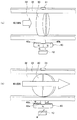
このため、本実施形態の磁気センサは、約−75°から約170°の範囲内で回転する回転角度の検出に利用されると好適であり、例えば、エンジンの燃焼室内に吸入される吸入空気量を制御するスロットルバルブの回転角度を検出するのに用いられると好適である。図4は、検出部10とスロットルバルブとの配置関係を示す模式図であり、(a)はスロットルバルブが完全に閉じている状態を示す図、(b)はスロットルバルブが完全に開いている状態を示す図である。
For this reason, the magnetic sensor of the present embodiment is preferably used for detection of a rotation angle that rotates within a range of about −75 ° to about 170 °. For example, intake air sucked into the combustion chamber of the engine It is preferably used for detecting the rotation angle of a throttle valve that controls the amount. 4A and 4B are schematic views showing the arrangement relationship between the
図4に示されるように、エンジンの燃焼室内に吸入される吸入空気量を制御するスロットルバルブ30は、スロットルバルブ30と共に回転するシャフト31と一体化されており、このシャフト31が吸入通路32を形成するスロットルボディー33に支持されることによって吸入通路32内に備えられている。ここでは、吸入通路32は吸入空気の流れの方向に対する断面が円形状とされ、スロットルバルブ30は完全に閉じているときに吸入空気を遮断することができるように吸入通路32とほぼ同じ径を有する円形板状とされている。また、シャフト31は、一端部側が吸入通路32外に突出するようにスロットルボディー33に備えられ、突出している先端部に永久磁石40を備えている。なお、永久磁石40が本発明の回転体に相当している。
As shown in FIG. 4, the
永久磁石40は、ここでは円板状とされており、径方向で同じ大きさに2分割されている。そして、2分割された一方がN極の永久磁石40aとされ、他方がS極の永久磁石40bとされており、図2(b)に示されるように、シャフト31を介してスロットルバルブ30と共に一体化して回転する。
The
検出部10は、永久磁石40が生成する外部磁界中に図示しない支持部材によって支持されて配置される。具体的には、第2、第3磁気抵抗素子R2、R3におけるピン層11の磁化方向がスロットルバルブ30が完全に閉じているときに永久磁石40が生成する外部磁界Bの方向と平行となるように配置される。
The
また、スロットルバルブ30は、図2に示されるように、一般的に完全に閉じている0°の状態から完全に開く90°の状態の間の範囲内を回転するものであり、上記磁気センサにおけるセンサ信号Voutの極大点と極小点との間の角度範囲を回転する。
Further, as shown in FIG. 2, the
したがって、本実施形態の磁気センサをスロットルバルブ30のような回転体の回転角度を検出するのに適用すると、arctan演算をするための複雑な装置、回路、プログラム等を必要とせず、簡素な構成で回転角度に対してリニアな信号を得ることができる。
Therefore, when the magnetic sensor of the present embodiment is applied to detect the rotation angle of a rotating body such as the
また、上記図3では、第1〜第4磁気抵抗素子R1〜R4の抵抗変化率αが80%であるものを説明したが、抵抗変化率αは適宜変更可能である。図5は、センサ信号Voutの電圧と磁場入射角度θとの関係を示す図であり、無磁界抵抗値R0を1としたときの各抵抗変化率αについてのシミュレーション結果である。なお、図5では、電源電圧Vccを1としている。 In FIG. 3, the first to fourth magnetoresistive elements R1 to R4 have been described in which the resistance change rate α is 80%. However, the resistance change rate α can be changed as appropriate. FIG. 5 is a diagram showing the relationship between the voltage of the sensor signal Vout and the magnetic field incident angle θ, and is a simulation result for each resistance change rate α when the magnetic field resistance value R 0 is 1. In FIG. 5, the power supply voltage Vcc is 1.
図5に示されるように、第1〜第4磁気抵抗素子R1〜R4の抵抗変化率αによって若干の違いはあるが、上記のように磁気センサを構成することにより、所定角度範囲内の磁場入射角度θに対してほぼリニアに変化するセンサ信号Voutを得ることができる。例えば、磁気抵抗率αが60%である場合は、センサ信号Voutの極大点である−70°から極小点である約165°の範囲において、センサ信号Voutは磁場入射角度θに対してほぼリニアに変化する信号となる。また、抵抗変化率が40%である場合は、センサ信号Voutの極大点である約−65°から極小点である約160°の範囲において、センサ信号Voutは磁場入射角度θに対してほぼリニアに変化する信号となる。つまり、抵抗変化率αによらず、所定角度範囲内では磁場入射角度θに対してほぼリニアに変化するセンサ信号Voutを得ることができる。 As shown in FIG. 5, although there is a slight difference depending on the resistance change rate α of the first to fourth magnetoresistive elements R1 to R4, a magnetic field within a predetermined angle range can be obtained by configuring the magnetic sensor as described above. A sensor signal Vout that changes substantially linearly with respect to the incident angle θ can be obtained. For example, when the magnetic resistivity α is 60%, the sensor signal Vout is substantially linear with respect to the magnetic field incident angle θ in a range from −70 ° which is the maximum point of the sensor signal Vout to about 165 ° which is the minimum point. The signal changes to. When the resistance change rate is 40%, the sensor signal Vout is substantially linear with respect to the magnetic field incident angle θ in a range from about −65 ° which is the maximum point of the sensor signal Vout to about 160 ° which is the minimum point. The signal changes to. That is, regardless of the resistance change rate α, it is possible to obtain a sensor signal Vout that changes substantially linearly with respect to the magnetic field incident angle θ within a predetermined angle range.
また、図6は磁場入射角度θと誤差との関係を示す図である。なお、誤差は、図5でプロットした点を用いた最小二乗法によって得られた直線に対する誤差である。図6に示されるように、各抵抗変化率αにおいて、磁場入射角度θが22.5°、67.5°、90°近傍のときに誤差が大きくなるが、抵抗変化率αが高いほど誤差が小さくなることが確認される。このため、第1〜第4磁気抵抗素子R1〜R4は、抵抗変化率αが高くなるように構成することが好ましい。 FIG. 6 is a diagram showing the relationship between the magnetic field incident angle θ and the error. The error is an error with respect to a straight line obtained by the method of least squares using the points plotted in FIG. As shown in FIG. 6, in each resistance change rate α, the error increases when the magnetic field incident angle θ is in the vicinity of 22.5 °, 67.5 °, and 90 °, but the error increases as the resistance change rate α increases. Is confirmed to be small. For this reason, it is preferable that the first to fourth magnetoresistive elements R1 to R4 are configured to have a high resistance change rate α.
以上説明したように、本実施形態の磁気センサでは、第1、第2磁気抵抗素子R1、R2は、ピン層11の磁化方向が互いに直交する状態でハーフブリッジ回路を構成するように電気的に直列接続されている。また、第3、第4磁気抵抗素子R3、R4は、ピン層11の磁化方向が互いに直交し、かつ第3磁気抵抗素子R3におけるピン層11の磁化方向が第2磁気抵抗素子R2におけるピン層11の磁化方向と平行となると共に第4磁気抵抗素子R4におけるピン層11の磁化方向が第1磁気抵抗素子R1におけるピン層11の磁化方向と平行となる状態でハーフブリッジ回路を構成するように電気的に直列接続されている。
As described above, in the magnetic sensor of this embodiment, the first and second magnetoresistive elements R1 and R2 are electrically configured so as to form a half-bridge circuit in a state where the magnetization directions of the pinned
そして、信号処理部20における差動増幅器21で第1、第2磁気抵抗素子R1、R2の中点電圧VAと第3、第4磁気抵抗素子R3、R4の中点電圧VBとを差動増幅し、差動増幅した結果をセンサ信号Voutとして出力している。
The first
このため、上記図3および図5に示されるように、所定角度範囲内の磁場入射角度θに対してほぼリニアに変化するセンサ信号Voutを出力することができる。 Therefore, as shown in FIGS. 3 and 5, it is possible to output the sensor signal Vout that changes substantially linearly with respect to the magnetic field incident angle θ within a predetermined angle range.
また、このような磁気センサは、従来の磁気センサに対して、第1〜第4磁気抵抗素子R1〜R4の配置方法を変更すると共に、オペアンプ等のような簡易な構成の差動増幅器21を備えるのみでよく、arctan演算を行うための複雑な装置、回路、プログラム等を必要としないため、構成を簡素化することができる。さらに、arctan演算のような演算を行わないため、応答速度を向上させることができる。
Such a magnetic sensor is different from the conventional magnetic sensor in that the arrangement method of the first to fourth magnetoresistive elements R1 to R4 is changed and a
(第2実施形態)
本発明の第2実施形態について説明する。本実施形態は、第1実施形態に対して検出部10を第1、第2磁気抵抗素子R1、R2および第1、第2抵抗で構成したものであり、その他に関しては第1実施形態と同様であるため、ここでは説明を省略する。図7は、本実施形態における磁気センサの回路構成を示す図である。
(Second Embodiment)
A second embodiment of the present invention will be described. In the present embodiment, the
図7に示されるように、本実施形態の検出部10は、上記第1実施形態に対して第3、第4磁気抵抗素子R3、R4の代わりに第1、第2抵抗R5、R6を備えたものであり、第1、第2磁気抵抗素子R1、R2および第1、第2抵抗R5、R6でフルブリッジ回路が構成されている。
As shown in FIG. 7, the
そして、差動増幅器21の反転入力端子には、第1、第2抵抗R5、R6の中点電圧VBが入力されるようになっている。本実施形態では、第1、第2抵抗R5、R6の抵抗値は等しくされており、差動増幅器21の反転入力端子にはVcc/2が入力される。
Then, to the inverting input terminal of the
なお、差動増幅器21の反転入力端子に入力される電圧は、Vcc/2に限定されるものではなく、適宜変更可能である。例えば、第1、第2磁気抵抗素子R1、R2の温度特性と同じ温度特性を有する電圧を入力することができる。具体的には、第1、第2抵抗R5、R6を第1、第2磁気抵抗素子R1、R2の温度特性と同じ温度特性を有する抵抗とすることができる。これにより、第1、第2磁気抵抗素子R1、R2の温特補正を行うことができ、検出精度を向上させることができる。
The voltage input to the inverting input terminal of the
このような磁気センサとしても、所定角度範囲内の磁場入射角度θに対してほぼリニアに変化するセンサ信号Voutを出力することができ、上記第1実施形態と同様の効果を得ることができる。図8は、第1、第2磁気抵抗素子R1、R2の中点電圧VAおよびセンサ信号Voutの電圧と磁場入射角度θとの関係を示すシミュレーション結果である。なお、図8では、無磁界抵抗値R0を1としたときの抵抗変化率αを無磁界抵抗値の80%とし、電源電圧Vccを1としている。 Even with such a magnetic sensor, it is possible to output a sensor signal Vout that changes substantially linearly with respect to the magnetic field incident angle θ within a predetermined angle range, and the same effects as in the first embodiment can be obtained. FIG. 8 is a simulation result showing the relationship between the midpoint voltage V A of the first and second magnetoresistive elements R1 and R2, the voltage of the sensor signal Vout, and the magnetic field incident angle θ. In FIG. 8, the resistance change rate α when the no-magnetic field resistance value R 0 is 1 is 80% of the no-magnetic field resistance value, and the power supply voltage Vcc is 1.
図8に示されるように、本実施形態の磁気センサでは、センサ信号Voutの極大点である約−80°から極小点である約170°の範囲において、センサ信号Voutは磁場入射角度θに対してほぼリニアに変化する信号となる。 As shown in FIG. 8, in the magnetic sensor of the present embodiment, the sensor signal Vout is relative to the magnetic field incident angle θ in a range from about −80 ° which is the maximum point of the sensor signal Vout to about 170 ° which is the minimum point. The signal changes almost linearly.
なお、上記図8では、第1、第2磁気抵抗素子R1、R2の中点電圧VAも示してあるが、中点電圧VAも極大点である約−80°から極小点である約170°の範囲で磁場入射角度θに対してほぼリニアに変化する信号となる。このため、磁気センサを検出部10のみで構成し、第1、第2磁気抵抗素子R1、R2の中点電圧VAをそのまま出力するようにしてもよい。このような磁気センサでは、信号処理部20を備える必要がないため、さらに磁気センサの構成を簡素化することができる。
In FIG. 8, the midpoint voltage V A of the first and second magnetoresistive elements R1 and R2 is also shown, but the midpoint voltage V A is also about a minimum point from about −80 ° which is a maximum point. The signal changes almost linearly with respect to the magnetic field incident angle θ in the range of 170 °. For this reason, the magnetic sensor may be configured by only the
(他の実施形態)
上記各実施形態では、磁気センサから磁場入射角度θに応じた電圧を出力する例について説明したが、次のようにしてもよい。すなわち、信号処理部20に変換部を備え、差動増幅器21から出力された電圧を磁場入射角度θに変換して出力するようにしてもよい。例えば、変換部を電圧とθとが対応付けられたマップを記憶している半導体メモリ等で構成することにより、差動増幅器21から出力される電圧を磁場入射角度θに変換して出力することができる。
(Other embodiments)
In each of the above-described embodiments, the example in which the voltage corresponding to the magnetic field incident angle θ is output from the magnetic sensor has been described. That is, the
また、上記各実施形態では、検出部10から出力された信号をオペアンプ等の差動増幅器21で差動増幅する、つまり、アナログ信号のまま差動増幅する例を説明した。しかしながら、検出部10から出力された信号をデジタル信号に変換した後に差動増幅(減算)するようにしてもよい。このように、検出部10から出力された信号をデジタル信号に変換した後に差動増幅するようにしても、従来のように、arctan演算を行う場合と比較すれば、単純な差動増幅(減算)を行うのみでよく、構成を簡素化することができる。
Further, in each of the above embodiments, an example has been described in which the signal output from the
さらに、上記第1実施形態おいて、第1〜第4磁気抵抗素子R1〜R4としてピン層11とフリー層13との間に導電体を挟んでなる巨大磁気抵抗素子(GMR素子)を用い、上記第2実施形態において、第1、第2磁気抵抗素子R1、R2としてピン層11とフリー層13との間に導電体を挟んでなる巨大磁気抵抗素子(GMR素子)を用いてもよい。
Furthermore, in the first embodiment, a giant magnetoresistive element (GMR element) in which a conductor is sandwiched between the pinned
また、上記第2実施形態では、第1磁気抵抗素子R1の抵抗値がR0+αsinθに変化し、第2磁気抵抗素子R2の抵抗値がR0+αcosθに変化するものを説明したが、第1磁気抵抗素子R1の抵抗値がR0+αcosθに変化し、第2磁気抵抗素子R2の抵抗値がR0+αsinθに変化するものであってもよい。図9は、他の実施形態におけるセンサ信号Voutの電圧と磁場入射角度θとの関係を示すシミュレーション結果である。 In the second embodiment, the resistance value of the first magnetoresistive element R1 changes to R 0 + αsinθ, and the resistance value of the second magnetoresistive element R2 changes to R 0 + αcosθ. The resistance value of the magnetoresistive element R1 may change to R 0 + αcos θ, and the resistance value of the second magnetoresistive element R2 may change to R 0 + αsin θ. FIG. 9 is a simulation result showing the relationship between the voltage of the sensor signal Vout and the magnetic field incident angle θ in another embodiment.
図9に示されるように、このような磁気センサとしても、センサ信号Voutの極小点である約−80°から極大点である約170°の範囲において、センサ信号Voutは磁場入射角度θに対してほぼリニアに変化する信号となる。また、図8と同様に、図9には第1、第2磁気抵抗素子R1、R2の間の中点電圧VAも示してあり、この中点電圧VAもセンサ信号Voutと同様に極大点である約−80°から極小点である約170°の範囲で磁場入射角度θに対してほぼリニアに変化する信号となる。したがって、磁気センサを検出部10のみで構成し、第1、第2磁気抵抗素子R1、R2の間の中点電圧VAをそのまま出力するようにしてもよい。
As shown in FIG. 9, even in such a magnetic sensor, the sensor signal Vout is in a range from about −80 ° which is the minimum point of the sensor signal Vout to about 170 ° which is the maximum point, with respect to the magnetic field incident angle θ. The signal changes almost linearly. Similarly to FIG. 8, FIG. 9 also shows the midpoint voltage V A between the first and second magnetoresistive elements R1 and R2, and this midpoint voltage V A is also the maximum as with the sensor signal Vout. The signal changes almost linearly with respect to the magnetic field incident angle θ in a range from about −80 ° as a point to about 170 ° as a minimum point. Therefore, the magnetic sensor may be configured by only the
R1〜R4 第1〜第4磁気抵抗素子
10 検出部
11 ピン層
13 フリー層
20 信号処理部
21 差動増幅器
R1 to R4 First to fourth
Claims (2)
前記第1、第2磁気抵抗素子(R1、R2)は、前記ピン層(11)の磁化方向が互いに直交する状態で直列接続されており、
前記検出部(10)は、磁化方向が前記第2磁気抵抗素子(R2)における前記ピン層(11)の磁化方向と同じ方向に固定されたピン層(11)および外部磁界に応じて磁化方向が変化するフリー層(13)を有し、前記ピン層(11)の磁化方向と前記フリー層(13)の磁化方向との成す角度に応じて抵抗値が変化し、前記第1磁気抵抗素子(R1)と共に電源に接続される第3磁気抵抗素子(R3)と、
磁化方向が前記第1磁気抵抗素子(R1)における前記ピン層(11)の磁化方向と同じ方向に固定されたピン層(11)および外部磁界に応じて磁化方向が変化するフリー層(13)を有し、前記ピン層(11)の磁化方向と前記フリー層(13)の磁化方向との成す角度に応じて抵抗値が変化し、前記第2磁気抵抗素子(R2)と共に接地されると共に前記第3磁気抵抗素子(R3)と直列接続される第4磁気抵抗素子(R4)と、を有し、
前記第1〜第4磁気抵抗素子(R1〜R4)によってフルブリッジ回路が構成されており、
前記第1、第2磁気抵抗素子(R1、R2)の中点電圧を第1検出信号として出力すると共に前記第3、第4磁気抵抗素子(R3、R4)の中点電圧を第2検出信号として出力し、
前記検出信号を用いて所定の演算を行う信号処理部(20)を備え、
前記信号処理部(20)は、前記第1検出信号から前記第2検出信号を減算する演算を行い、Vccを前記電源の電圧、R 0 を無磁界中における前記第1〜第4磁気抵抗素子(R1〜R4)の抵抗値、αを前記第1〜第4磁気抵抗素子(R1〜R4)の抵抗変化率、θを前記第2、第3磁気抵抗素子(R2、R3)におけるピン層と印加される外部磁界との成す角度としてη=θ−45°とすると、
The first and second magnetoresistive elements (R1, R2) are connected in series with the magnetization directions of the pinned layer (11) orthogonal to each other,
The detection unit (10) has a magnetization direction in accordance with an external magnetic field and a pinned layer (11) fixed in the same direction as the magnetization direction of the pinned layer (11) in the second magnetoresistive element (R2). The first magnetoresistive element has a free layer (13) that changes in resistance, and a resistance value changes according to an angle formed by the magnetization direction of the pinned layer (11) and the magnetization direction of the free layer (13). A third magnetoresistive element (R3) connected to the power supply together with (R1);
A pinned layer (11) whose magnetization direction is fixed in the same direction as the magnetization direction of the pinned layer (11) in the first magnetoresistive element (R1) and a free layer (13) whose magnetization direction changes according to an external magnetic field The resistance value changes according to the angle formed by the magnetization direction of the pinned layer (11) and the magnetization direction of the free layer (13), and is grounded together with the second magnetoresistive element (R2). A fourth magnetoresistive element (R4) connected in series with the third magnetoresistive element (R3),
A full bridge circuit is constituted by the first to fourth magnetoresistive elements (R1 to R4),
The midpoint voltage of the first and second magnetoresistive elements (R1, R2) is output as a first detection signal, and the midpoint voltage of the third and fourth magnetoresistive elements (R3, R4) is output as a second detection signal. Output as
A signal processing unit (20) for performing a predetermined calculation using the detection signal;
The signal processing unit (20) performs an operation of subtracting the second detection signal from the first detection signal, and Vcc is the voltage of the power source, and R0 is the first to fourth magnetoresistive elements in a non-magnetic field. The resistance value of (R1 to R4), α is the resistance change rate of the first to fourth magnetoresistive elements (R1 to R4), θ is the pinned layer in the second and third magnetoresistive elements (R2, R3), Assuming that η = θ−45 ° as an angle formed with the applied external magnetic field,
Priority Applications (4)
| Application Number | Priority Date | Filing Date | Title |
|---|---|---|---|
| JP2011227854A JP5866956B2 (en) | 2011-10-17 | 2011-10-17 | Magnetic sensor |
| CN201280051095.9A CN103890598B (en) | 2011-10-17 | 2012-08-28 | Magnetic sensor |
| PCT/JP2012/005385 WO2013057863A1 (en) | 2011-10-17 | 2012-08-28 | Magnetic sensor |
| US14/344,074 US20140340081A1 (en) | 2011-10-17 | 2012-08-28 | Magnetic sensor |
Applications Claiming Priority (1)
| Application Number | Priority Date | Filing Date | Title |
|---|---|---|---|
| JP2011227854A JP5866956B2 (en) | 2011-10-17 | 2011-10-17 | Magnetic sensor |
Publications (2)
| Publication Number | Publication Date |
|---|---|
| JP2013088232A JP2013088232A (en) | 2013-05-13 |
| JP5866956B2 true JP5866956B2 (en) | 2016-02-24 |
Family
ID=48140534
Family Applications (1)
| Application Number | Title | Priority Date | Filing Date |
|---|---|---|---|
| JP2011227854A Expired - Fee Related JP5866956B2 (en) | 2011-10-17 | 2011-10-17 | Magnetic sensor |
Country Status (4)
| Country | Link |
|---|---|
| US (1) | US20140340081A1 (en) |
| JP (1) | JP5866956B2 (en) |
| CN (1) | CN103890598B (en) |
| WO (1) | WO2013057863A1 (en) |
Families Citing this family (11)
| Publication number | Priority date | Publication date | Assignee | Title |
|---|---|---|---|---|
| JP2015049047A (en) * | 2013-08-29 | 2015-03-16 | アルプス電気株式会社 | Motor controller |
| CN105701904B (en) * | 2015-12-29 | 2018-03-30 | 威海华菱光电股份有限公司 | Magnetic image sensor |
| CN106772149B (en) * | 2016-11-18 | 2018-07-06 | 清华大学 | The very big Measurement Method for Magnetic Field and device of a kind of optimization |
| CN106556806B (en) * | 2016-11-18 | 2018-03-13 | 清华大学 | A kind of greatly Measurement Method for Magnetic Field and device |
| JP7186481B2 (en) * | 2018-05-18 | 2022-12-09 | 株式会社東海理化電機製作所 | Magnetic sensor device |
| CN109814047B (en) * | 2019-01-16 | 2024-05-17 | 北京麦格智能科技有限公司 | TMR sensor with low 1/f noise |
| JP6886222B2 (en) * | 2019-03-19 | 2021-06-16 | Tdk株式会社 | Magnetic sensor |
| JP7070532B2 (en) * | 2019-11-19 | 2022-05-18 | Tdk株式会社 | Magnetic sensor |
| JP7173104B2 (en) * | 2020-07-21 | 2022-11-16 | Tdk株式会社 | magnetic sensor |
| JP7281492B2 (en) * | 2021-01-20 | 2023-05-25 | Tdk株式会社 | How to design a magnetic sensor |
| CN115754848B (en) * | 2022-11-17 | 2024-04-02 | 江苏多维科技有限公司 | Magnetic sensor |
Family Cites Families (11)
| Publication number | Priority date | Publication date | Assignee | Title |
|---|---|---|---|---|
| DE19619806A1 (en) * | 1996-05-15 | 1997-11-20 | Siemens Ag | Magnetic field sensitive sensor device with several GMR sensor elements |
| DE60037790T2 (en) * | 1999-06-18 | 2009-01-08 | Koninklijke Philips Electronics N.V. | MAGNETIC MEASURING SYSTEM WITH IRREVERSIBLE CHARACTERISTICS, AND METHOD FOR THE PRODUCTION, REPAIR AND USE OF SUCH A SYSTEM |
| JP4543350B2 (en) * | 1999-12-03 | 2010-09-15 | 日立金属株式会社 | Rotation angle sensor and rotation angle sensor unit |
| JP2004103769A (en) * | 2002-09-09 | 2004-04-02 | Fujitsu Ltd | CPP structure magnetoresistive element |
| CN100429799C (en) * | 2002-10-18 | 2008-10-29 | 雅马哈株式会社 | Magnetic inductor and its manufacturing method |
| JP4557134B2 (en) * | 2004-03-12 | 2010-10-06 | ヤマハ株式会社 | Manufacturing method of magnetic sensor, magnet array used in manufacturing method of magnetic sensor, and manufacturing method of magnetic array |
| JP4293037B2 (en) * | 2004-04-13 | 2009-07-08 | 株式会社デンソー | Rotation detector |
| JP2007024598A (en) * | 2005-07-13 | 2007-02-01 | Denso Corp | Magnetic sensor |
| JP4984962B2 (en) * | 2007-02-27 | 2012-07-25 | 大同特殊鋼株式会社 | Magnetic angle sensor |
| US8715776B2 (en) * | 2007-09-28 | 2014-05-06 | Headway Technologies, Inc. | Method for providing AFM exchange pinning fields in multiple directions on same substrate |
| FR2955942B1 (en) * | 2010-01-29 | 2013-01-04 | Centre Nat Rech Scient | INTEGRATED MAGNETOMETER AND METHOD FOR MANUFACTURING THE SAME |
-
2011
- 2011-10-17 JP JP2011227854A patent/JP5866956B2/en not_active Expired - Fee Related
-
2012
- 2012-08-28 CN CN201280051095.9A patent/CN103890598B/en not_active Expired - Fee Related
- 2012-08-28 US US14/344,074 patent/US20140340081A1/en not_active Abandoned
- 2012-08-28 WO PCT/JP2012/005385 patent/WO2013057863A1/en active Application Filing
Also Published As
| Publication number | Publication date |
|---|---|
| CN103890598B (en) | 2016-05-04 |
| CN103890598A (en) | 2014-06-25 |
| WO2013057863A1 (en) | 2013-04-25 |
| US20140340081A1 (en) | 2014-11-20 |
| JP2013088232A (en) | 2013-05-13 |
Similar Documents
| Publication | Publication Date | Title |
|---|---|---|
| JP5866956B2 (en) | Magnetic sensor | |
| JP5120384B2 (en) | Rotation angle detection device, rotator, and rotation angle detection method | |
| JP5780760B2 (en) | Matching of GMR sensors at the bridge | |
| JP6698859B2 (en) | Device for detecting the angular position of rotatable components | |
| US8860410B2 (en) | Circuits and methods for processing a signal generated by a plurality of measuring devices | |
| CN105785290B (en) | Magnetic field sensor | |
| US6661225B2 (en) | Revolution detecting device | |
| US20090284254A1 (en) | Magnetic sensor | |
| CN103575210B (en) | Position detector | |
| US20220381800A1 (en) | Amr speed and direction sensor for use with magnetic targets | |
| JP2009150795A (en) | Noncontact type rotation angle detection sensor device and its output correction method | |
| JP2021516333A (en) | Systems and methods for reducing angular error with respect to magnetic field angle sensors | |
| CN110388943A (en) | Encoder | |
| JP7242352B2 (en) | A system for determining at least one rotational parameter of a rotating member | |
| JP2010133851A (en) | Rotation angle sensor | |
| CN111693910B (en) | System for determining at least one rotation parameter of a rotating component | |
| Sreekantan et al. | Magnetic sensors and industrial sensing applications | |
| JP2014066565A (en) | Magnetic sensor | |
| JP5212452B2 (en) | Rotation sensor | |
| CN111693909B (en) | System for determining at least one rotation parameter of a rotating component | |
| JP5434943B2 (en) | Rotation sensor | |
| JP2013096898A (en) | Rotation angle detection apparatus for throttle valve | |
| US20140125328A1 (en) | Magnetic detection device | |
| JP2016206012A (en) | Magnetism detection device | |
| JP5195787B2 (en) | Rotation sensor |
Legal Events
| Date | Code | Title | Description |
|---|---|---|---|
| A621 | Written request for application examination |
Free format text: JAPANESE INTERMEDIATE CODE: A621 Effective date: 20140904 |
|
| A131 | Notification of reasons for refusal |
Free format text: JAPANESE INTERMEDIATE CODE: A131 Effective date: 20150616 |
|
| A521 | Request for written amendment filed |
Free format text: JAPANESE INTERMEDIATE CODE: A523 Effective date: 20150806 |
|
| TRDD | Decision of grant or rejection written | ||
| A01 | Written decision to grant a patent or to grant a registration (utility model) |
Free format text: JAPANESE INTERMEDIATE CODE: A01 Effective date: 20151208 |
|
| A61 | First payment of annual fees (during grant procedure) |
Free format text: JAPANESE INTERMEDIATE CODE: A61 Effective date: 20151221 |
|
| R151 | Written notification of patent or utility model registration |
Ref document number: 5866956 Country of ref document: JP Free format text: JAPANESE INTERMEDIATE CODE: R151 |
|
| R250 | Receipt of annual fees |
Free format text: JAPANESE INTERMEDIATE CODE: R250 |
|
| R250 | Receipt of annual fees |
Free format text: JAPANESE INTERMEDIATE CODE: R250 |
|
| LAPS | Cancellation because of no payment of annual fees |