JP5787629B2 - Multi-processor system on chip for machine vision - Google Patents
Multi-processor system on chip for machine vision Download PDFInfo
- Publication number
- JP5787629B2 JP5787629B2 JP2011127961A JP2011127961A JP5787629B2 JP 5787629 B2 JP5787629 B2 JP 5787629B2 JP 2011127961 A JP2011127961 A JP 2011127961A JP 2011127961 A JP2011127961 A JP 2011127961A JP 5787629 B2 JP5787629 B2 JP 5787629B2
- Authority
- JP
- Japan
- Prior art keywords
- data
- memory
- main memory
- local memory
- unit
- Prior art date
- Legal status (The legal status is an assumption and is not a legal conclusion. Google has not performed a legal analysis and makes no representation as to the accuracy of the status listed.)
- Active
Links
Images


Classifications
-
- G—PHYSICS
- G06—COMPUTING OR CALCULATING; COUNTING
- G06F—ELECTRIC DIGITAL DATA PROCESSING
- G06F15/00—Digital computers in general; Data processing equipment in general
- G06F15/16—Combinations of two or more digital computers each having at least an arithmetic unit, a program unit and a register, e.g. for a simultaneous processing of several programs
- G06F15/163—Interprocessor communication
- G06F15/167—Interprocessor communication using a common memory, e.g. mailbox
-
- G—PHYSICS
- G06—COMPUTING OR CALCULATING; COUNTING
- G06F—ELECTRIC DIGITAL DATA PROCESSING
- G06F15/00—Digital computers in general; Data processing equipment in general
- G06F15/76—Architectures of general purpose stored program computers
- G06F15/80—Architectures of general purpose stored program computers comprising an array of processing units with common control, e.g. single instruction multiple data processors
-
- G—PHYSICS
- G06—COMPUTING OR CALCULATING; COUNTING
- G06F—ELECTRIC DIGITAL DATA PROCESSING
- G06F9/00—Arrangements for program control, e.g. control units
- G06F9/06—Arrangements for program control, e.g. control units using stored programs, i.e. using an internal store of processing equipment to receive or retain programs
- G06F9/30—Arrangements for executing machine instructions, e.g. instruction decode
- G06F9/38—Concurrent instruction execution, e.g. pipeline or look ahead
- G06F9/3802—Instruction prefetching
-
- G—PHYSICS
- G06—COMPUTING OR CALCULATING; COUNTING
- G06F—ELECTRIC DIGITAL DATA PROCESSING
- G06F9/00—Arrangements for program control, e.g. control units
- G06F9/06—Arrangements for program control, e.g. control units using stored programs, i.e. using an internal store of processing equipment to receive or retain programs
- G06F9/30—Arrangements for executing machine instructions, e.g. instruction decode
- G06F9/38—Concurrent instruction execution, e.g. pipeline or look ahead
- G06F9/3885—Concurrent instruction execution, e.g. pipeline or look ahead using a plurality of independent parallel functional units
Landscapes
- Engineering & Computer Science (AREA)
- Theoretical Computer Science (AREA)
- Computer Hardware Design (AREA)
- Software Systems (AREA)
- Physics & Mathematics (AREA)
- General Engineering & Computer Science (AREA)
- General Physics & Mathematics (AREA)
- Multi Processors (AREA)
- Memory System Of A Hierarchy Structure (AREA)
- Computing Systems (AREA)
- Memory System (AREA)
Description
本発明は、一般的にマルチプロセッサシステムに関し、特にマルチプロセッサシステムにおける共用資源の効率的使用のための方法及びシステムに関するものである。 The present invention relates generally to multiprocessor systems, and more particularly to methods and systems for efficient use of shared resources in multiprocessor systems.
完全なマルチプロセッサシステムの実行、特に単一モノリシックデバイスにおける対称多重処理(SMP)システムは、VLSIデバイスの過密化と、リアルタイムのマシンビジョンのような複雑化するコンピュータ業務により、近年盛んになってきた。あるマルチプロセッサシステムでは、メモリ資源は複数のプロセッサに共用される。しかしこのような共用は、メモリのコヒーレンシー問題を引き起こし、性能のボトルネックとなる。 Execution of a complete multiprocessor system, in particular a symmetric multiprocessing (SMP) system in a single monolithic device, has become popular in recent years due to overcrowding of VLSI devices and complex computer tasks such as real-time machine vision . In some multiprocessor systems, memory resources are shared by multiple processors. However, such sharing causes memory coherency problems and becomes a performance bottleneck.
特許文献1は、それはここに参照され採り入れられるが、バスベースのキャッシュコヒーレンスプロトコルを使用して大規模SMPシステムの分散システム構造を開示している。分散システム構造は、アドレススイッチ、多重メモリサブシステム、及び、多重マスターデバイスを含み、プロセッサ、I/Oエージェント、又はコヒーレントなメモリアダプターのいずれかは、ノードコントローラにサポートされたノードの1組に編成される。ノードコントローラは1つのマスターデバイスからのトランザクションを受け取り、他の1つのマスターデバイスとして、又は、スレーブデバイスとして1つのマスターデバイスと通信し、そしてマスターデバイスから受け取ったトランザクションの順番の列を作る。コヒーレンシーの達成が時間と空間に配分されるため、ノードコントローラはキャッシュコヒーレンシーを維持する補助をする。更に、標準バスコントロールに対するトランザクションタグフォーマットが拡張され、一意のトランザクションタグがシステムを通して維持される。ある場合には、ノードコントローラにおいてトランザクションタグを保存するために、サイドバンド信号が干渉と再実行に使用される。 U.S. Patent No. 6,057,031, which is incorporated herein by reference, discloses a distributed system structure for large scale SMP systems using a bus-based cache coherence protocol. Distributed system structure, address switch, multiple memory subsystems, and includes a multiplex master device, the processor, I / O agents, or any of the coherent memory adapter, set to organize support node to node controller Is done. Node controller receives a transaction from one master device, as another one master device, or to communicate with one master device and a slave device, and queuing the order of transactions received from the master device. The node controller helps maintain cache coherency because the achievement of coherency is distributed in time and space. In addition, the transaction tag format for standard bus control is extended and unique transaction tags are maintained throughout the system. In some cases, sideband signals are used for interference and re-execution to save the transaction tag at the node controller.
特許文献2は、それはここに参照され採り入れられるが、単一プログラムメモリを含む同一のプロセッサからなる並行マルチプロセッシング構造を持つSMPシステムを開示している。プログラムアクセス調停ロジックは一度に1つの命令を単一の要求元CPUに供給する。共用メモリアクセス調停ロジックは、データを異なる同時アクセス可能なメモリバンクから供給し、又は複数のCPUの中でアクセスを調停することができる。システムは、共用メモリの中の既定の1組のアドレスへの読み取りアクセスに続く既定数のメモリサイクルの期間、他の1つのCPUによる1つのアドレスへのアクセスを禁止することによりアトミックな読み取り/修正/書込み命令をシミュレートしてもよい。 U.S. Patent No. 6,099,056, which is incorporated herein by reference, discloses an SMP system having a parallel multiprocessing structure consisting of the same processor including a single program memory. Program access arbitration logic supplies one instruction at a time to a single requesting CPU. The shared memory access arbitration logic can supply data from different simultaneously accessible memory banks or arbitrate access among multiple CPUs. System, atomic by prohibiting access default set of predetermined number of notes period recycle following the read access to the address in the co-memory, the one address by one other CPU read / A modify / write command may be simulated.
本発明のある実施形態では、メインメモリと多重のプロセシングコアを含むマルチプロセッサシステムを提供する。多重のプロセシングコアは、メインメモリに記憶されるデータを使用するソフトウェアを実行するように設定される。 データストリーミングユニットは、プロセシングコアとメインメモリの間を接続し、多重のプロセシングコアによる使用のため、データをメインメモリから事前に取得するように設定される。 One embodiment of the present invention provides a multiprocessor system that includes a main memory and multiple processing cores. Multiple processing cores are configured to execute software that uses data stored in main memory. The data streaming unit is configured to connect between the processing core and the main memory and to obtain data in advance from the main memory for use by multiple processing cores.
ある実施形態では、データストリーミングユニットが、プロセシングコアのためにデータをメインメモリ内に記憶するように設定される。ある実施形態では、データストリーミングユニットが、2つ以上のプロセシングコアのために実行される、メインメモリに対する同時アクセスを解決するように設定される調停回路を有する。
ある実施形態では、データストリーミングユニットが、それぞれのプロセシングコアに対し、メインメモリ内のアドレスのそれぞれ1つのリストをプロセシングコアから受け取り、リストに従ってメインメモリよりデータを事前取得するように設定される、それぞれ1つのフロントエンドユニットを有する。
In some embodiments, the data streaming unit is configured to store data in main memory for the processing core. In some embodiments, the data streaming unit has an arbitration circuit configured to resolve simultaneous access to main memory that is executed for two or more processing cores.
In an embodiment, the data streaming unit is configured to receive a respective list of addresses in main memory from the processing core for each processing core and pre-acquire data from the main memory according to the list, respectively. It has one front end unit.
開示された実施形態では、それぞれのプロセシングコアに付随するそれぞれ1つのローカルメモリを有し、それぞれのプロセシングコアと対応するフロントエンドユニットは、それぞれのローカルメモリ経由でデータを交換するように設定される。
ある実施形態では、それぞれのプロセシングコアと対応するフロントエンドユニットは、アドレスのリストをそれぞれのローカルメモリ内に記憶される1つの循環バッファ内に維持するように設定される。ある実施形態では、少なくともプロセシングコアとデータストリーミングユニットが単一の半導体内に含まれる。
In the disclosed embodiment, each front-end unit associated with each processing core has a local memory associated with each processing core and is configured to exchange data via the respective local memory. .
In one embodiment, each processing core and corresponding front-end unit is configured to maintain a list of addresses in one circular buffer stored in each local memory. In some embodiments, at least the processing core and the data streaming unit are included in a single semiconductor.
本発明のある実施形態によれば、メインメモリと多重のプロセシングコアを含むマルチプロセッサシステムが提供される。多重のプロセシングコアは、メインメモリに記憶されるデータを使用するソフトウェアを実行するように設定される。スクラッチパッドプロセスユニットは、プロセシングコアに接続し、そして、多重のプロセシングコアのために、2つ以上のプロセシングコアに同時に1つの所与のデータアイテムにアクセスさせる、ソフトウェアの選択された部分を実行するように設定される。 In accordance with one embodiment of the present invention, a multiprocessor system is provided that includes a main memory and multiple processing cores. Multiple processing cores are configured to execute software that uses data stored in main memory. A scratchpad process unit connects to processing cores and executes selected portions of software that cause two or more processing cores to access a given data item simultaneously for multiple processing cores Is set as follows.
ある実施形態では、スクラッチパッドプロセスユニットが、2つ以上のプロセシングコアにアクセスされる所与のデータアイテムを記憶するための独自のメモリを有する。ある実施形態では、スクラッチパッドプロセスユニットが、スクラッチパッド命令をプロセシングコアから受信し、スクラッチパッド命令を調停し、そして、独自のメモリ内の調停されたスクラッチパッド命令を実行するように設定される。開示された実施形態では、少なくともプロセシングコアとスクラッチパッドプロセスユニットが単一半導体内に含まれる。 In some embodiments, the scratch pad process unit has its own memory for storing a given data item that is accessed by more than one processing core. In one embodiment, the scratch pad process unit is configured to receive a scratch pad instruction from the processing core, arbitrate the scratch pad instruction, and execute the arbitrated scratch pad instruction in its own memory. In the disclosed embodiment, at least the processing core and the scratch pad process unit are included in a single semiconductor.
本発明のある実施形態によればさらに、あるデータ処理方法が提供される。その方法は、マルチプロセッサシステムの多重プロセシングコア上で、メインメモリに記憶されるデータを使用するソフトウェアを実行するステップと、多重プロセシングコアによる使用のため、プロセシングコアとメインメモリの間を接続するデータストリーミングユニットにより、データをメインメモリから事前に取得するステップと、を有する。 According to an embodiment of the present invention, a data processing method is further provided. The method includes the steps of executing software using data stored in main memory on a multiprocessing core of a multiprocessor system, and data connecting between the processing core and main memory for use by the multiprocessing core. Pre-acquiring data from the main memory by the streaming unit.
本発明のある実施形態によればさらに、あるデータ処理方法が提供される。その方法は、マルチプロセッサシステムの多重プロセシングコア上で、メインメモリに記憶されるデータを使用するソフトウェアを実行するステップと、多重プロセシングコアに接続し、プロセシングコアのために、2つ以上のプロセシングコアに同時に1つの所与のデータアイテムにアクセスさせる、ソフトウェアの選択された部分を実行する、スクラッチパッドプロセスユニットを使用するステップと、を有する。
本発明は、図を参照した本発明の実施形態の以下の詳細な説明により十分に理解されよう。
According to an embodiment of the present invention, a data processing method is further provided. The method includes the steps of executing software using data stored in main memory on a multiple processing core of a multiprocessor system, and connecting to the multiple processing core for the processing core. Using a scratchpad process unit to execute a selected portion of software that allows a given data item to be accessed simultaneously.
The invention will be more fully understood from the following detailed description of embodiments of the invention with reference to the drawings.
(概論)
あるマルチプロセッサシステムは、単一の集積回路(システムオンチップ、SOC)として実現される。SOCは典型的にローカルメモリユニットの1つ以上のインスタンスからなるが、ローカルメモリよりはるかに大規模な可能性のあるメインメモリは含まない。メインメモリは典型的に、1つ以上の集積回路により実現され、シーケンシャルな(バースト)アクセスに対し高帯域幅を許容するが、長いレイテンシを持つ。マルチプロセッサシステムにおいてこのようなメインメモリが複数のプロセッサにより共用される場合、メモリへのアクセス待ちの結果としての大幅な性能の劣化を避けるため、効率的な調停が行われなければならない。
(Introduction)
Some multiprocessor systems are implemented as a single integrated circuit (system on chip, SOC). An SOC typically consists of one or more instances of local memory units, but does not include main memory , which can be much larger than local memory. The main memory is typically implemented by one or more integrated circuits, but allows a high bandwidth to sequential (burst) access, with a long latency. When such main memory is shared by multiple processors in a multiprocessor system, efficient arbitration must be performed to avoid significant performance degradation as a result of waiting for access to the memory.
本発明の実施形態は、共用メモリにアクセスする複数のプロセッサにより引き起こされた、性能ボトルネックを緩和する新規の方法を紹介する。本発明の実施形態によれば、マルチプロセッサシステムは、プロセッサコア(プロセシングコア)により必要とされる前にメインメモリからデータを取得するデータストリーミングユニット(DSU)を有する。DSUは取得したデータをプロセッサコアに接続したローカルメモリに記憶し、そこではデータはプロセッサコアにより必要に応じてアクセス可能である。DSUはまた、ローカルメモリからメインメモリにデータを書込み可能である。 Embodiments of the present invention introduce a novel method for mitigating performance bottlenecks caused by multiple processors accessing shared memory. According to embodiments of the present invention, a multiprocessor system has a data streaming unit (DSU) that obtains data from main memory before being required by a processor core (processing core). The DSU stores the acquired data in a local memory connected to the processor core, where the data can be accessed by the processor core as needed. The DSU can also write data from local memory to main memory.
マルチプロセッサシステムに付随する他の問題は、2つ以上のプロセッサが同じメモリ位置にアクセスする場合に、メモリのコヒーレンシーを確実にすることである。マルチプロセッサシステムで実行されるある画像処理向けアルゴリズムでは、複数のプロセッサコアによるメインメモリ内の同じアドレスへのアクセスはまれであり、それは例えば、複数のプロセッサコアにより処理される画像領域から画像統計を集めるタスクにおいて発生する。それでもこのようなまれな場合でも、効率よく処理されないと性能のボトルネックを生じる。 Another problem associated with multiprocessor systems is ensuring memory coherency when two or more processors access the same memory location. In an image processing for algorithm executed by a multiprocessor system, accesses to the same address in the main memory by a plurality of processor cores are rare, it is, for example, the image statistics from the image area to be processed by a plurality of processor cores Occurs in the collect task. Nevertheless, even in such rare cases, performance bottlenecks arise if they are not handled efficiently.
本発明の実施形態はこのようなボトルネックを緩和する新規の方法を紹介する。開示された実施形態によれば、共用メモリ位置への全てのアクセスは、スクラッチ−パッドユニットにより取り扱われ、それは、専用プロセッサと小規模ローカルメモリからなり、共用メモリ位置にアクセスする並行タスクの実行用に最適化されたソフトウェアを実行する。クラッチ−パッドユニットは典型的にマルチプロセッサシステムのプロセッサコアにコプロセッサとして付属する。 Embodiments of the present invention introduce a novel method for mitigating such bottlenecks. According to the disclosed embodiment, all accesses to the shared memory location are handled by a scratch-pad unit, which consists of a dedicated processor and small local memory for executing concurrent tasks that access the shared memory location. Run optimized software. The clutch-pad unit is typically attached as a coprocessor to the processor core of a multiprocessor system.
(システムの記述)
図1は本発明の実施形態による、マルチプロセッサシステム10の概略ブロック図である。マルチプロセッサシステム10の全ての図示された要素は、1つの集積回路上に配置可能であり、システムオンチップを構成する。
マルチプロセッサシステム10は、メインメモリ500(「外部メモリ」とも呼ばれる)を有する。ある実施形態では、メインメモリ500は、1つ以上の異なる集積回路からなり、マルチプロセッサSOCの一部ではない。他の実施形態では、メインメモリとマルチプロセッサシステム10の他の要素は同一のSOC内に配置される。更に他の実施形態では、メインメモリ500は、複数の部品からなり、それらの幾つかはSOC内に配置され、幾つかは1つ以上の外部チップ内に配置される。以下の記載では、「外部メモリ」という言葉は、メインメモリに対して使用される。しかし本発明はSOCに搭載されないメインメモリに限定されない。
(System description)
FIG. 1 is a schematic block diagram of a
The
SOC内に配置されるメモリコントローラ400は、外部メモリに対するアクセスを制御し、そしてある実施形態では、記憶リフレッシュ機構、及び他のメモリ制御機能を提供する。ある実施形態では、ローカルメモリユニット300がそれぞれのプロセッサコア200に付属する。それぞれのローカルメモリユニットは、例えばコードセグメントを充足させるため、メモリコントローラ400経由で、ダイレクトメモリアクセス(DMA)チャネルを使用して外部メモリ500にアクセスしてもよい。
A
本発明の実施形態によれば、メインメモリ内の共用メモリ位置へのアクセスの結果としての性能劣化はデータストリーミングユニット(DSU)2000によって低減される。DSU2000は、ローカルメモリユニット300(各プロセッサコアに1つ)に事前に、典型的にはプロセッサコア200がそのデータにアクセスを必要とする時間より前に、外部メモリ500からのデータを入れ、それにより外部メモリへのアクセス上の読み取り競合の結果としてのプロセッサコア200の遅れを最小化する、ように構成されてもよい。同様に、DSU2000は、プロセッサコア200によりローカルメモリユニット300に書き込まれたデータを外部メモリ500に送り、それにより外部メモリへのアクセスに対する書込み競合の結果としてのプロセッサコア200の遅れを最小化してもよい。
According to embodiments of the present invention, performance degradation as a result of accessing shared memory locations in main memory is reduced by data streaming unit (DSU) 2000. The
DSU2000は、メモリコントローラ400へのアクセスを支配するDSUアービター2200と、DSUフロントエンドユニット2100からなり、ここで各フロントエンドユニットはそれぞれ1つのローカルメモリ300とそれぞれ1つのプロセッサコア200に接続する。
DSU2000 includes a
ある実施形態では、共用メモリ位置へのアクセスはスクラッチ−パッドユニット1000により取り扱われ、それは、それぞれのプロセッサコア200にそれぞれ接続する命令バッファ1300を有する。スクラッチ−パッドユニット1000は、1つ以上のスクラッチ−パッドRAM1100と、1つ以上のスクラッチ−パッドコントローラ1200を有し、それぞれのスクラッチ−パッドRAMは、命令バッファ1300にそれぞれのスクラッチ−パッドコントローラ1200を経由して接続する。
In one embodiment, access to shared memory locations is handled by the scratch-
典型的な実施形態では、命令バッファ1300は、現在の命令が要求先クラッチ−パッドコントローラに対する調停に勝つまで、プロセッサコア200により生成された命令を一時的に記憶する(命令に付随する標的アドレスに従って)。図1の実施形態では、(必須ではないが)、それぞれのプロセッサコア200はそれぞれ専用の命令バッファ1300に接続している。一度命令が命令バッファでバッファされると、バッファはバッファ済み命令に付随する標的アドレスに従って適切なスクラッチ−パッドコントローラ1200にアクセスを要求する。アクセスが与えられると、命令はその命令バッファからそのスクラッチ−パッドコントローラに実行のため送られる。
In a typical embodiment,
スクラッチ−パッドユニット1000は、共通する共用メモリマルチプロセッサタスクを、共通する共用メモリタスクを最適に実行するように接続されたスクラッチ−パッドコントローラ1200が独立して実行することを許容し、それによりプロセッサコア200の負荷を軽減し、効率的なメモリーロック機構を導入することによりメモリコヒーレンスを保証する。この技術は、メモリが物理的にロックされていないため効率的である。開示された技術は、読み取り−修正−書込みの完全なサイクルがコントローラによりアトミックに実行されることを保証する。
The scratch-
(データストリーミングユニット(DSU))
図2は本発明の実施形態による、データストリーミングユニット(DSU)2000と、それに接続するメモリコントローラ400、プロセッサコア200、及びローカルメモリユニット300を含むユニットの概略ブロック図である。
DSU2000は、それぞれのプロセッサコア200とそれに付随するローカルメモリ300にそれぞれサービスを提供する複数のDSUフロントエンドユニット2100、とDSUフロントエンドユニット2100により開始されたメモリアクセス要求を調停する単一のDSUアービター2200からなる。
(Data streaming unit (DSU))
FIG. 2 is a schematic block diagram of a unit including a data streaming unit (DSU) 2000 and a
The
プロセッサコアは初期化において、DSUがデータをメモリからローカルメモリに移動するようにプログラムする。その後DSU2000はデータを外部メモリ500からローカルメモリ300に事前ロードして、外部メモリへの読み取りアクセスの競合を減少させ、そして結果的にマルチプロセッサシステム10の性能を向上させる。同様にプロセッサコアは、DSUがデータをローカルメモリから外部メモリに移動するように事前プログラムし、外部メモリへの書込みアクセスの競合を減少させる。
At initialization, the processor core programs the DSU to move data from memory to local memory. The
この構成は、幾つかの理由で性能を向上させる。例えば、外部メモリ500とのトラフィックは全てのトラフィックを知る単一のコントローラ(DSUアービター)により最適化可能である。更に、プロセッサコア200は、必要なデータが事前に取得されているため、渋滞で失速せず、それによりデータアクセスのレイテンシを低下させる。
This configuration improves performance for several reasons. For example, traffic with the
プロセッサコア200による外部メモリ内のアドレスからの全ての読み取り動作は、外部メモリ500からの対応する読み取り動作及びローカルメモリ300への対応する書込み動作が終了した後に実行され、それらは共にDSUフロントエンドユニット2100により実行される。同様に、ローカルプロセッサによる外部メモリ内のアドレスへの全ての書込み動作の後に、ローカルメモリからの対応する読み取り及びその後の外部メモリへの書込みが実行され、それらは共にDSUにより実行される。
All read operations from the addresses in the external memory by the
ある実施形態では、プロセッサコア200と外部メモリ500間のデータ転送は、ローカルメモリ内に配置される複数の循環バッファにより実行される。その様子を図3に示す。それぞれのプロセッサコアは、データをそれぞれの循環バッファ内に書き込み、そしてDSUはデータを循環バッファから読み取り、それをメインメモリに書き込む。メインメモリが外部メモリである実施形態では、これは外部メモリコントローラ400により実行される。読み取り動作に対しては、DSUはデータをメインメモリから読み取り(メインメモリが外部メモリである場合は外部メモリコントローラ経由で)、そしてそれを循環バッファに書き込む。プロセッサコアは循環バッファから取得されたデータを読み取る。
In an embodiment, data transfer between the
図3は、本発明の実施形態による、循環バッファ310の構造を示す概略図である。本発明の実施形態では、複数の循環バッファが各ローカルメモリ内で実施されてもよい。ある所与のローカルメモリ300に配置される循環バッファは、DSUフロントエンドユニット2100及びこのローカルメモリに接続するプロセッサコア200により管理される。図3とそれに続く記述における「読み取り」と「書込み」という言葉は、ローカルプロセッサコア200により実行される「読み取り」と「書込み」を意味する。
FIG. 3 is a schematic diagram illustrating the structure of the
循環バッファは、バッファがスタートするローカルメモリ300内の1つの場所を指し示す出発ポインタ311と、ローカルメモリ300内の最後の位置を示す終了ポインタ316とを有する。バッファは循環式であり、バッファへの連続アクセスに対しては、終了ポインタ316の次の場所は出発ポインタ311である。
The circular buffer has a
ローカルプロセッサコア200により処理されるデータ要素は、現在要素ポインタ313により指し示されるが、それは(以下に記述される)特別のプロセッサコア命令により前進させられる。ローカルプロセッサに対する有効データを含む作業ウィンドウ314が定義される。現在要素ポインタ313が読み取りポインタの値に到達すると、プロセッサは新しいデータが到着するまで待機させられる。更に、読み取りポインタ315の値が書込みポインタ312の値と同一の場合、外部メモリからの読み取りデータの更なる取得は、書込みポインタが前進するまで延期される。
Data elements processed by the
図4は、本発明の実施形態による、DSUフロントエンドユニット2100の概略ブロック図である。DSUフロントエンドに接続するローカルプロセッサコア200とローカルメモリ300も示されている。それぞれのDSUフロントエンド2100は、DSUバッファ管理ユニット2110、制御ユニット2130、バッファ選択マルチプレクサ2140、及び外部メモリアクセス制御2150からなる。DSUフロントエンドユニット2100はローカルプロセッサコア200により1リストのタスクを実行するように設定される;このような設定は、制御ユニット2130に配置される複数のレジスタのプログラミングを含み、ここで各レジスタは読み取り、書込み及びデータ寸法及び各循環バッファ310用の出発ポインタと終了ポインタの値を示唆するビットを含む。
FIG. 4 is a schematic block diagram of a DSU
DSUバッファ管理ユニット2110は、以下で詳述されるが、循環バッファ310を管理する。ユニット2110は、バッファ終了ポインタをバッファ出発ポインタにラップアラウンドして、読み取り及び書込みポインタを増加させ、そして、NLI(1)命令(後述)がプロセッサコアから受信された場合、再びバッファ終了ポインタをラップアラウンドして、現在要素ポインタを増加させる。現在要素ポインタに対する増加がその値を読み取りポインタの値と同じにさせる場合、バッファ管理ユニット2110はプロセッサコア200に信号を送り新しいデータが受信されるまで待機させる。
The DSU
制御ユニット2130は、ローカルメモリ300へのアクセスを必然的に伴う循環バッファ310へのアクセスを調停する。このような調停は、例えば、回転優先順位方式により実施される。
バッファ選択マルチプレクサ2140は、制御ユニット2130から選択されたバッファへのポインタを得て、そして前記バッファにより生成されたアドレスをローカルメモリ300に出力する。
The
制御ユニット2130はまた、読み取り、書込み要求を生成し、DSUアービター2200から読み取り応答を獲得する、外部メモリアクセス制御2150を制御する。外部メモリアクセス制御2150からのデータは、ローカルメモリ300に送られてもよい;しかし、外部メモリとの間で読み取り、書込みされたデータ寸法がローカルメモリのデータポートの寸法と異なる場合、追加のバッファ/ロジック(不図示)が使用されてもよい。
The
図5は、本発明の実施形態によるDSUバッファ管理ユニット2110の概略ブロック図である。バッファ管理ユニット2110は、DSUフロントエンド2100内に内蔵され、そして複数の循環バッファへのアクセスを制御する。ある実施形態では、DSUバッファ管理ユニット2110は、複数の同じ単一バッファマネジャユニット(SBM)2120からなり、各SBMはローカルメモリ300内の単一のそれぞれの循環バッファを制御する。SBM2120は、読み取りポインタ315の値を保持する読み取りポインタ(RP)レジスタ2123、書込みポインタ312の値を保持する書込みポインタ(WP)レジスタ2122、現在要素ポインタ(CEP)313の値を保持する現在要素ポインタ(CEP)レジスタ2124からなる。読み取りポインタ(RP)は、DSUフロントエンド2100が外部メモリから読み取ったデータを書き込む、次のメモリ位置を示し、また、書込みポインタ(WP)は、DSUフロントエンド2100がその後外部メモリに書き込むデータを読み取る、次のメモリ位置を示す。
FIG. 5 is a schematic block diagram of a DSU
SBM2120はさらに、現在のデータトランザクションで送信されるデータユニットの寸法を記憶する(例えばバイト数で)寸法レジスタ2121と、寸法レジスタ2121に記憶される値をポインタレジスタ2122、2123、2124内の値に加算し、それにより各トランザクション後にそれらを更新する、加算子2126と、コンパレータ2125とを含む。コンパレータ2125は、CEPレジスタ2124の値をRPレジスタの値と比較し、それらが同じ場合「待機」出力を主張し、それによりプロセッサコア200は待機させられる。
The
読み取り及び書込みポインタレジスタ2122,2123の更新は、セレクト(Select)入力により適格とされ、制御ユニット2130により起動される(図4参照)、ここでそれぞれのSBM2120に対し1つの異なるセレクトラインがある;セレクトラインは所定のセレクト(選択)−1、セレクト−2、以下同様、である。セレクトラインに加えて制御ユニット2130は、全てのSBMに対して共通の制御ライン:選択されたSBM2120の書込みポインタレジスタ2122と読み取りポインタレジスタ2123をそれぞれ更新するための、読み取りと書き込みと;DSUフロントエンドユニット2100の全てのSBM2120の全てのCEPレジスタ2124を更新するためのNLI(1)と;を主張する。
Updating of the read and write
図4に戻り、制御ユニット2130はDSUフロントエンドユニット2100内で事前にプログラムされたタスクを実行する。制御ユニットは、プロセッサコア200により1リストのメモリ送信タスクで事前に構成される;制御ユニットはその後、DSUバッファ管理ユニット2110から、例えば回転優先順位方式などの1つの基準に従ってポインタを選択する。制御ユニットはその後、選択されたアドレスをローカルメモリ300に出力するため、バッファ選択マルチプレクサ2140のアドレス入力を制御し、そして1つの指示ワード、それはバッファのインデックスや読み取り/書込みビットを含んでもよいが、を外部メモリアクセス制御2150に送信する。さらに、いずれかのSBM2120が停止(ストール)出力を設定した場合、制御ユニットはその動作を停止が解除されるまで停止すため、プロセッサコア200に対し集合停止(ストール)出力を主張する。
Returning to FIG. 4, the
初期化において実行されるDSUの構成に加えて、制御ユニット2130は、2つの特別なプロセッサ命令により制御される:NLI(0)及びNLI(1)。NLI(1)は、循環バッファ内で現在要素ポインタ(CEP)313を進ませるために使用される。それは、プロセッサが次の値を計算するため新しい1組のパラメータを必要とする場合、プログラムループのそれぞれの繰り返しの後にセットされる。
In addition to the configuration of the DSU executed at initialization, the
更新されたパラメータは、全ての活性化したSBMの現在要素ポインタ(CEP)を含む。更新は典型的に全てのSBMを一括して単一サイクルで、そして循環バッファラップの位置を考慮して実行される。NLI命令は、現在要素ポインタ(CEP)の新しい位置が外部メモリから取得した要求されたデータで充足されていることを認証する。そうでない場合プロセッサコアは、読み取りポインタ(RP)と現在要素ポインタ(CEP)が要求基準(即ち、RPがCEPより大きい)を満たすまで待機する。 The updated parameters include the current element pointer (CEP) of all activated SBMs. Updates are typically performed in a single cycle for all SBMs in bulk and taking into account the location of the circular buffer wrap. The NLI instruction authenticates that the new position of the current element pointer (CEP) is filled with the requested data obtained from the external memory. Otherwise, the processor core waits until the read pointer (RP) and current element pointer (CEP) meet the required criteria (ie, RP is greater than CEP).
NLI(1)は、制御ユニット2130によりDSUバッファ管理ユニット2110に対して指示される。NLI(0)は、プロセッサコア200によりプログラムがスタートする時に発せられる。NLI(0)命令の目的は、初期のCEPが処理に対して有効である(即ち、要求されたデータが外部メモリから読み取り済みでローカルメモリに書き込み済みである)ことを認証することである。
NLI (1) is instructed to the DSU
読み取りポインタ(RP)315及び書込みポインタ(WP)312は典型的に、NLI(0)が受信されるまでそれらの初期位置から進まない。(RPはそれが第1の要素を処理するためのデータを取得する必要があるため増加される。WPはCEPがまだ初期の位置を指し示し、その位置はWPが指し示す位置と同じあるため増加されない。処理されたデータはまだ無いので、外部メモリには何も書き込まれない。) Read pointer (RP) 315 and write pointer (WP) 312 typically do not advance from their initial positions until NLI (0) is received. (RP is incremented because it needs to get data to process the first element. WP is not incremented because CEP still points to the initial position and that position is the same as the position pointed to by WP. (There is no processed data yet, so nothing is written to the external memory.)
外部メモリアクセス制御2150は制御ユニット2130により起動されDSUアービター2200に対する読み取り及び書込み要求を開始する;それはまたDSUアービター2200から読み取り応答を取得し、読み取りデータをローカルメモリに伝達する。
External
図6は本発明の実施形態による、DSUアービター2200の概略ブロック図である。DSUアービター2200は読み取り及び書込み要求を複数のDSUフロントエンド2100から受信し、要求の間を調停し、外部メモリ内の対応するアドレスを計算し、外部メモリアクセス要求を外部メモリコントローラ400に送信する。またDSUアービターは、外部メモリコントローラから受信した読み込み要求に対する応答を要求元DSUフロントエンドに戻す。本発明のある実施形態では、書込み応答は必要なく、書込み要求は受け入れられたと見做される。他の実施形態では、図6に図示されていないが、書込み応答が取り扱われ、(以下に記述する)読み取り応答ラッチ2210に類似したユニットがDSUアービター2200に追加される。
FIG. 6 is a schematic block diagram of a
複数のDSUフロントエンド2100からの読み取り要求は、読み取り要求ラッチ2230内にラッチされる。本発明の実施形態では、読み取り要求ラッチ2230は、それぞれのDSUフロントエンドユニットに対して、どの循環バッファに要求が対応しているかを示す1つのインデックスと、要求が有効でまだ未処理であることを示す1つのペンディングビットを含む。読み取り要求ラッチ2230からの要求は、読み取り要求調停ユニット2250に入力され、それは、例えば、回転優先順位方式を使用して、複数の同時発生の読み取り要求の間を調停する。読み取り要求調停はまた、読み取り要求ラッチ2230内の選択された要求のペンディングビットを消去する。
Read requests from multiple DSU front ends 2100 are latched in
(以下で説明されるが、1つ又はそれ以上の)選択された読み取り操作は、読み取りアドレス計算ユニット2270に出力され、それは、外部メモリに対するポインタ(それぞれのローカルメモリ300内のそれぞれの循環バッファに対し1つのポインタ)を維持し更新し、そしてポインタ値及び外部メモリの編成に関するパラメータに基づいて、外部メモリ内のアドレスを計算する; 本発明のある実施形態では、処理されたオブジェクトがビデオ画像であり、これらパラメータは、画像幅、高さ、ピクセル当りバイト数を含む。読み取りアドレス計算ユニットからの出力は、外部メモリコントローラ400への読み取り要求である。
The selected read operation (described below, but one or more) is output to a read
本発明のある実施形態では、外部メモリへのアクセスのバンド幅はローカルメモリ300内のバンド幅より大きい;これは幅広のバス、速いクロック、又はそれらの組合せに由来する。このような実施形態では、同時に複数のメモリアクセスを生成することが望ましい。このような実施形態では、読み取り要求調停ユニット2250は、幾つかの読み取り要求を選択し、そして読み取りアドレス計算ユニット2270は、幾つかのトランザクション用のアドレスを同時に計算する。
In some embodiments of the invention, the bandwidth of access to external memory is greater than the bandwidth in
書込み要求の方式は、読み取り要求について記載されたものと類似しており、書込み要求をラッチするための書込み要求ラッチ2220、未処理の書込み要求間を調停する書込み要求調停ユニット2240、及び外部メモリ内のアドレスを計算する、書込みアドレス計算ユニット2260を含む。本発明のある実施形態では、書込み要求ラッチ2220、書込み要求調停ユニット2240及び書込みアドレス計算ユニット2260は、それぞれ読み取り要求ラッチ2230、読み取り要求調停ユニット2250及び読み取りアドレス計算ユニット2270と同一でよい。他の実施形態では、各ユニットが性質は類似しているが、書込みは読み取りより頻度が少ないため、書込み関連ユニットの実装は低いエリア及び性能に最適化されてもよい。
The write request scheme is similar to that described for read requests, a
最後に、読み取り応答ラッチ2210は、外部メモリコントローラ400からの読み取り要求応答をラッチし、そしてその応答を要求元のそれらDSUフロントエンド2100に出力する。
Finally, read
(スクラッチパッドユニット)
本発明の実施形態では、共用メモリ資源にアクセスするマルチプロセッサシステム10のプログラムは、スクラッチパッドユニット1000により取り扱われ、それは、メモリのコヒーレンシーを保証し、共用メモリ資源へのアクセスに伴う遅れを緩和する。スクラッチパッドユニットは、要するに、共用メモリタスクの効率的な実行、及びメモリのコヒーレンシーの保証に対し最適化された命令セットを有する、特別目的プロセッサである。
(Scratch pad unit)
In an embodiment of the present invention,
図7は、本発明の実施形態による、スクラッチパッドユニット1000及びプロセッサコア200に対するインタフェースの概略ブロック図である。1組のスクラッチパッド命令(以下で「SP命令」と呼ぶ)は、プロセッサコア200に対して定義される。SP命令は、プロセッサコア200により命令バッファ1300に送信され、命令バッファはその後実行のためそれらをスクラッチパッドコントローラ1200に送信する。
FIG. 7 is a schematic block diagram of an interface to the
プロセッサコア200は、バッファが従前の命令をスクラッチパッドコントローラ1200に送信していなかった場合、或いは、従前の命令が戻り値を期待する命令であり、かつその戻り値がまだ獲得されていない場合、新しいSP命令を接続する命令バッファに送信することを控える。この方式は例えば、適切なプロセッサコアを配置することにより、ハードウェアで実行されてもよい。
If the buffer has not sent a previous instruction to the
命令バッファ1300は、SP命令を2つのスクラッチパッドコントローラ1200の内の1つに送信する。スクラッチパッドコントローラは、複数の命令バッファ1300からの複数の命令の間を調停し、その中の1つを実行のため選択する。本発明のある実施形態によれば、調停は回転優先度法を使用する。
The
偶数のスクラッチパッドメモリ位置を参照する命令は、偶数スクラッチパッドコントローラ1200に出力され、一方奇数のスクラッチパッドメモリ位置を参照する命令は、奇数スクラッチパッドコントローラ1200に出力される。従って、命令で特定されるアドレスの最下位ビットは、スクラッチパッドコントローラには送信されず、その代わり、2つのコントローラの内の1つを選択するのに使用される。
Instructions that refer to even scratch pad memory locations are output to the even
それぞれのスクラッチパッドコントローラ1200は、スクラッチパッドメモリ又はその一部である、RAM1100に接続している。本発明のある実施形態では、スクラッチパッドメモリは奇数及び偶数アドレスに従ってインターリーブされている;一方のRAM1100が偶数アドレスを保持し(図7でRAM偶数と表示)、他方のRAM1100が奇数アドレスを保持する(図7でRAM奇数と表示)。RAM偶数に接続するスクラッチパッドコントローラ1200は、「スクラッチパッドコントローラ偶数」と呼ばれ、そしてRAM奇数に接続するスクラッチパッドコントローラ1200は、「スクラッチパッドコントローラ奇数」と呼ばれる。本発明の他の実施形態では、他のタイプのインターリーブ方式が使用されてもよい。例えば、2つの最下位のアドレスビットに従った4グルーブへの分離や、ハッシング関数による分離がある。
Each
あるSP命令は要求元プロセッサに値を返す。その目的のため、それぞれのスクラッチパッドコントローラ1200は、戻り値を全てのプロセッサコア200に出力する。さらに、それぞれのプロセッサコアが、入力データがそのプロセッサが発した命令に対する戻り値であるかを決定するため、それぞれのスクラッチパッドコントローラ1200は、RAMからの戻りデータが目的地とするプロセッサのIDコードをIDバス上で主張し、そのIDコードは全てのプロセッサコア200に出力される。調停が与えられた後、そのスクラッチパッドコントローラ内のレイテンシが定められる。従って、他の実施形態では、命令バッファは、サイクルを数え、そしてこのサイクル数に従ってデータを獲得してもよい。
Some SP instructions return a value to the requesting processor. For that purpose, each
表1は、本発明のある実施形態における9つのSP命令のリストである。それぞれのSP命令は、種々のSP命令を識別し、4ビットからなる1つのオペレーションコードと、スクラッチパッドメモリ内のアドレスであり、例えば16−18ビットからなる1つのインデックス、及び1−2つのオペランドからなる。 Table 1 is a list of nine SP instructions in one embodiment of the present invention. Each SP instruction identifies a different SP instruction, which is one operation code consisting of 4 bits, an address in the scratchpad memory, for example one index consisting of 16-18 bits, and 1-2 operands Consists of.
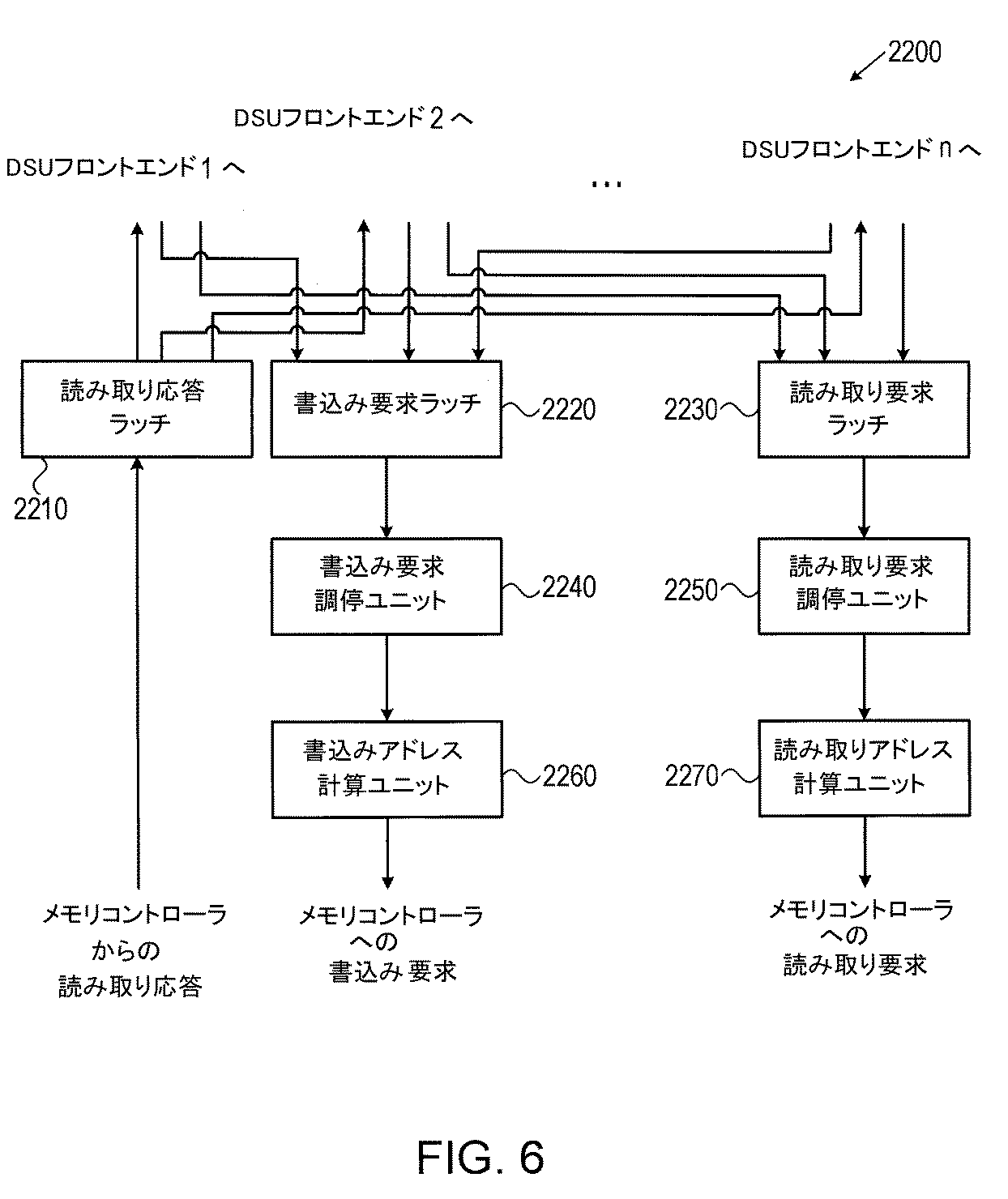
図8は、本発明の実施形態による、スクラッチパッドコントローラ1200のパイプラインステージと構造を示す概略ブロック図である。スクラッチパッドコントローラ1200は、回転優先順位アービター1210(アービター)、読み取りステージユニット1220、実行ステージユニット1230、書込みステージユニット1240、コンパレータ1260及びマルチプレクサ1250からなる。スクラッチパッドコントローラ1200は、パイプライン構造を有し、命令の実行はパイプラインステージで行われる。書込みステージユニット1240が命令nの結果を書き込むと、実行ステージユニット1230は命令n+1の一部を実行し、読み取りステージユニット1220はメモリアドレスから命令n+2で特定されたデータを取得し、アービター1210は命令n+3を命令バッファ1300より獲得する。
8, according to an embodiment of the present invention, is a schematic block diagram showing the pipes line stages and structure of
アービター1210は命令バッファからの命令入力の間を調停し、そして、例えば、回転優先度法を使用する。アービターが1つの命令ソースを選択するとアービターは、選択された命令を読み取りステージユニット1220に送信し、レディー出力を主張する。それは、命令バッファに対し命令バッファが次の命令を(存在する場合)適用可能であることを示す。
アービター1210から読み取りステージユニット1220に送信された命令は、5つのフィールドからなる。そのうち最初の4つのフィールドは選択された命令からコピーされ、1つのオペコードフィールド、1つのインデックスフィールド、及び1−2つのオペランド−OP1及びOP2からなる;上記表1は各命令により使用されるフィールドを示す。5番目のフィールドは、選択された命令バッファを識別し、戻り値の命令元のプロセッサコアへのルートづけを可能にする、1つのIDフィールドである。
The command transmitted from the
読み取りステージユニット1220は、1クロックの遅延の後、アービターから受信した命令のフィールドを実行ステージユニット1230に出力する。更に、読み取りステージユニット1220は、オペランドのアドレスが、スクラッチパッドメモリから、RAM1100の読み取りアドレスポートに接続する読み取りアドレスバス上で取得されることを主張する。アドレスはアービター1210からのインデックスフィールド出力と同一でもよい。RAMから読み取られたデータは、(以下に記述される)マルチプレクサ1250を経由して実行ステージユニット1230に送信される;RAM1100を経由する遅延は1クロックなので、RAMからのデータとそれぞれの命令とは実行ステージユニット1230に同じクロックサイクルで到達する。
The read
実行ステージユニット1230は、命令を実行し、その命令は、ロジック/算術動作の実行(必要な場合)、RAM1100から読み取られた戻り値の出力、及び書込みステージユニット1240の起動を含んでよい。戻り値は、命令開始元のプロセッサのIDと共に、全てのプロセッサコア200に出力される。
書込みステージユニット1240は、命令が書込み部分を有する場合にのみ起動される。書込みステージユニットは実行ステージユニットからメモリ位置のインデックス(アドレス)と書込みデータを、書込み起動信号と共に受信する。書込みが要求される場合は、実行ステージユニット1230は書込み出力を主張し、そして、RAM1100の書込みアドレスポート上に書込みアドレスを書込みデータポート上に書込みデータを主張して、アドレス(インデックス)とデータを送信する。
The
メモリコヒーレンシー機構は、1つの命令がメモリからデータを読み取り、一方で従前の命令により新しいデータが同じ場所に書き込まれる場合に呼び出される;パイプラインにより課された1クロックの遅延のため、両方のアクセスは同じクロックサイクルで起こる。コンパレータ1260は、書込みアドレスと読み込みアドレスを比較する;2つのアドレスが同じ場合、マルチプレクサ1250は書き込まれたデータを直接実行ステージユニット1230に送り、RAM1100から読み取られたデータは無視される。
Memory coherency mechanism, one instruction read-data from the memory, whereas if the invoked new data by previous instructions Ru written to the same location; for 1 clock delay imposed by the pipeline, both Access occurs in the same clock cycle.
図1−8に示されるシステム10の構成及び種々のシステム要素の構成は、例示であり、思想の明確化のためにのみ選択された。他の実施形態では、他の適合する構成が使用可能である。ある実施形態では、ここに記載のコントローラやプロセッサ、例えばメモリコントローラ400、プロセッサコア200、スクラッチパッドコントローラ1200は、ここに記載の機能を実行するためのソフトウェアでプログラムされた汎用プロセッサからなってもよい。ソフトウェアはプロセッサに電子形態で、例えばネット上でダウンロードされてもよく、或いはさらに、磁気、光学、又は電子メモリのような非一過性の接触可能媒体上で提供され及び/又は記憶されてもよい。
The configuration of
ここに記載された実施形態は、主にSOCマルチプロセッサシステムについて記述しているが、ここに記載された方法とシステムは、幾つかの集積回路に分散され、バス又はネットワーク又はそれらの組合せにより相互接続されたマルチプロセッサシステムのような、他のアプリケーションにも使用可能である。
上記の実施形態は事例のために引用され、本発明はここに特に示され記載されたものに限定されない。むしろ本発明の範囲は、上記の種々の特徴の組合せ及びサブ組合せを含み、また、上記記載を読んだ当業者が想起する、従来技術に無い変化形や変更を含む。
Although the embodiments described herein primarily describe an SOC multiprocessor system, the methods and systems described herein are distributed over several integrated circuits and interact with each other by a bus or network or combination thereof. It can also be used for other applications such as connected multiprocessor systems.
The above embodiments are cited for purposes of example and the present invention is not limited to what has been particularly shown and described herein. Rather, the scope of the present invention includes combinations and subcombinations of the various features described above, as well as variations and modifications not found in the prior art that will occur to those skilled in the art upon reading the above description.
10:マルチプロセッサシステム 200:ローカルプロセッサコア
300:ローカルメモリ 311:出発ポインタ
312:書込みポインタ 313:現在要素ポインタ
314:作業ウィンドウ 315:読み取りポインタ
316:終了ポインタ 400:メモリコントローラ
500:メインメモリ、外部メモリ
1000:スクラッチ−パッドユニット
1100:スクラッチ−パッドRAM
1200:スクラッチ−パッドコントローラ
1210:アービター 1220:読み取りステージユニット
1230:実行ステージユニット 1240:書込みステージユニット
1250:マルチプレクサ 1260:コンパレータ
1300:命令バッファ
2000:DSU
2100:DSUフロントエンドユニット
2110:DSUバッファ管理ユニット
2120:単一バッファマネジャユニット(SBM)
2121:寸法レジスタ
2122:書込みポインタ(WP)レジスタ
2123:読み取りポインタ(RP)レジスタ
2124:現在要素ポインタ(CEP)レジスタ
2125:コンパレータ
2126:加算子
2130:制御ユニット
2140:バッファ選択マルチプレクサ
2150:外部メモリアクセス制御
2200:DSUアービター
2210:読み取り応答ラッチ
2220:書込み要求ラッチ
2230:読み取り要求ラッチ
2240:書込み要求調停ユニット
2250:読み取り要求調停ユニット
2260:書込みアドレス計算ユニット
2270:読み取りアドレス計算ユニット
10: Multiprocessor system 200: Local processor core 300: Local memory 311: Departure pointer 312: Write pointer 313: Current element pointer 314: Work window 315: Read pointer 316: End pointer 400: Memory controller 500: Main memory, external memory
1000: Scratch-pad unit 1100: Scratch-pad RAM
1200: Scratch-pad controller 1210: Arbiter 1220: Read stage unit 1230: Execution stage unit 1240: Write stage unit 1250: Multiplexer 1260: Comparator 1300: Instruction buffer 2000: DSU
2100: DSU front-end unit 2110: DSU buffer management unit 2120: Single buffer manager unit (SBM)
2121: Dimension register
2122: Write pointer (WP) register 2123: Read pointer (RP) register 2124: Current element pointer (CEP) register 2125: Comparator 2126: Adder 2130: Control unit 2140: Buffer selection multiplexer 2150: External memory access control 2200: DSU Arbiter 2210: Read response latch 2220: Write request latch 2230: Read request latch 2240: Write request arbitration unit 2250: Read request arbitration unit 2260: Write address calculation unit 2270: Read address calculation unit
Claims (14)
前記メインメモリに記憶されるデータを使用するソフトウェアを実行するように設定された、多重のプロセシングコアと、
それぞれのプロセシングコアに付随するそれぞれ1つのローカルメモリと、
前記プロセシングコアと前記メインメモリの間を接続し、前記多重のプロセシングコアによる使用のため、前記データを前記メインメモリから事前に取得するように設定された、データストリーミングユニットと、
を有し、
前記データストリーミングユニットは、前記データを前記各ローカルメモリ内に記憶される循環バッファへ書き込み、前記データを当該巡回バッファから読み出すことにより、前記各ローカルメモリを介して各プロセッシングコアと前記データを交換するように構成される、ことを特徴とする、マルチプロセッサシステム。 Main memory,
Multiple processing cores configured to execute software that uses data stored in the main memory;
One local memory associated with each processing core;
A data streaming unit connected between the processing core and the main memory and configured to obtain the data in advance from the main memory for use by the multiple processing cores;
I have a,
The data streaming unit exchanges the data with each processing core via each local memory by writing the data to a circular buffer stored in each local memory and reading the data from the circular buffer. A multiprocessor system, characterized by being configured as follows.
前記多重プロセシングコアによる使用のため、前記プロセシングコアと前記メインメモリの間を接続するデータストリーミングユニットにより、前記データを前記メインメモリから事前に取得するステップと、
を有し、
前記データを事前に取得するステップは、各プロセシングコアに関連づけられる各ローカルメモリに記憶される巡回バッファへ前記データを書き込み、当該巡回バッファから前記データを読み込むことにより、前記各ローカルメモリを介して前記データストリーミングユニットと各プロセッシングコアとの間で前記データを交換するステップを含むことを特徴とする、データ処理方法。 Executing software using data stored in main memory on a multiprocessing core of a multiprocessor system;
Pre-obtaining the data from the main memory by a data streaming unit connecting the processing core and the main memory for use by the multiple processing core;
I have a,
The step of acquiring the data in advance includes writing the data to a cyclic buffer stored in each local memory associated with each processing core, and reading the data from the cyclic buffer, whereby the data is read via the local memory. A data processing method comprising the step of exchanging said data between a data streaming unit and each processing core .
Applications Claiming Priority (4)
| Application Number | Priority Date | Filing Date | Title |
|---|---|---|---|
| US37256310P | 2010-08-11 | 2010-08-11 | |
| US61/372,563 | 2010-08-11 | ||
| US13/074,034 US9075764B2 (en) | 2010-08-11 | 2011-03-29 | Multiprocessor system-on-a-chip for machine vision algorithms |
| US13/074,034 | 2011-03-29 |
Publications (3)
| Publication Number | Publication Date |
|---|---|
| JP2012038293A JP2012038293A (en) | 2012-02-23 |
| JP2012038293A5 JP2012038293A5 (en) | 2014-07-03 |
| JP5787629B2 true JP5787629B2 (en) | 2015-09-30 |
Family
ID=45565631
Family Applications (1)
| Application Number | Title | Priority Date | Filing Date |
|---|---|---|---|
| JP2011127961A Active JP5787629B2 (en) | 2010-08-11 | 2011-06-08 | Multi-processor system on chip for machine vision |
Country Status (5)
| Country | Link |
|---|---|
| US (1) | US9075764B2 (en) |
| JP (1) | JP5787629B2 (en) |
| KR (1) | KR101753913B1 (en) |
| CN (1) | CN102375800B (en) |
| TW (1) | TWI528279B (en) |
Families Citing this family (28)
| Publication number | Priority date | Publication date | Assignee | Title |
|---|---|---|---|---|
| US9857868B2 (en) | 2011-03-19 | 2018-01-02 | The Board Of Trustees Of The Leland Stanford Junior University | Method and system for ergonomic touch-free interface |
| US8840466B2 (en) | 2011-04-25 | 2014-09-23 | Aquifi, Inc. | Method and system to create three-dimensional mapping in a two-dimensional game |
| US8854433B1 (en) | 2012-02-03 | 2014-10-07 | Aquifi, Inc. | Method and system enabling natural user interface gestures with an electronic system |
| EP2817785B1 (en) | 2012-02-23 | 2019-05-15 | Charles D. Huston | System and method for creating an environment and for sharing a location based experience in an environment |
| US10937239B2 (en) | 2012-02-23 | 2021-03-02 | Charles D. Huston | System and method for creating an environment and for sharing an event |
| US10600235B2 (en) | 2012-02-23 | 2020-03-24 | Charles D. Huston | System and method for capturing and sharing a location based experience |
| US9098739B2 (en) | 2012-06-25 | 2015-08-04 | Aquifi, Inc. | Systems and methods for tracking human hands using parts based template matching |
| US9111135B2 (en) | 2012-06-25 | 2015-08-18 | Aquifi, Inc. | Systems and methods for tracking human hands using parts based template matching using corresponding pixels in bounded regions of a sequence of frames that are a specified distance interval from a reference camera |
| US8836768B1 (en) | 2012-09-04 | 2014-09-16 | Aquifi, Inc. | Method and system enabling natural user interface gestures with user wearable glasses |
| US9092665B2 (en) | 2013-01-30 | 2015-07-28 | Aquifi, Inc | Systems and methods for initializing motion tracking of human hands |
| US9129155B2 (en) | 2013-01-30 | 2015-09-08 | Aquifi, Inc. | Systems and methods for initializing motion tracking of human hands using template matching within bounded regions determined using a depth map |
| US9298266B2 (en) | 2013-04-02 | 2016-03-29 | Aquifi, Inc. | Systems and methods for implementing three-dimensional (3D) gesture based graphical user interfaces (GUI) that incorporate gesture reactive interface objects |
| US9798388B1 (en) | 2013-07-31 | 2017-10-24 | Aquifi, Inc. | Vibrotactile system to augment 3D input systems |
| US9507417B2 (en) | 2014-01-07 | 2016-11-29 | Aquifi, Inc. | Systems and methods for implementing head tracking based graphical user interfaces (GUI) that incorporate gesture reactive interface objects |
| US9619105B1 (en) | 2014-01-30 | 2017-04-11 | Aquifi, Inc. | Systems and methods for gesture based interaction with viewpoint dependent user interfaces |
| US10523585B2 (en) | 2014-12-19 | 2019-12-31 | Amazon Technologies, Inc. | System on a chip comprising multiple compute sub-systems |
| US10394731B2 (en) | 2014-12-19 | 2019-08-27 | Amazon Technologies, Inc. | System on a chip comprising reconfigurable resources for multiple compute sub-systems |
| US11200192B2 (en) | 2015-02-13 | 2021-12-14 | Amazon Technologies. lac. | Multi-mode system on a chip |
| US9588921B2 (en) * | 2015-02-17 | 2017-03-07 | Amazon Technologies, Inc. | System on a chip comprising an I/O steering engine |
| CN104951424A (en) * | 2015-07-09 | 2015-09-30 | 天津瑞发科半导体技术有限公司 | Computer system provided with multiple processors and common external memory |
| TWI655548B (en) * | 2017-10-13 | 2019-04-01 | 技嘉科技股份有限公司 | Controlling circuit and operation method for arranging priority and solving the signal conflict in the protocol interface |
| US10866900B2 (en) * | 2017-10-17 | 2020-12-15 | Samsung Electronics Co., Ltd. | ISA extension for high-bandwidth memory |
| CN113835898B (en) * | 2017-11-29 | 2024-03-01 | 北京忆芯科技有限公司 | Memory distributor |
| TWI719741B (en) * | 2019-12-04 | 2021-02-21 | 財團法人工業技術研究院 | Processor and method of changing redundant processing node |
| US20230058920A1 (en) * | 2021-08-18 | 2023-02-23 | Samsung Electronics Co., Ltd. | System and method for halting processing cores in a multicore system |
| CN114817120A (en) * | 2022-06-29 | 2022-07-29 | 湖北芯擎科技有限公司 | Cross-domain data sharing method, system-on-chip, electronic device and medium |
| US12530308B2 (en) | 2023-07-25 | 2026-01-20 | Analog Devices, Inc. | Dataflow gaskets for handling data streams |
| CN117312330B (en) * | 2023-11-29 | 2024-02-09 | 中国人民解放军国防科技大学 | Vector data aggregation method and device based on note storage and computer equipment |
Family Cites Families (17)
| Publication number | Priority date | Publication date | Assignee | Title |
|---|---|---|---|---|
| JPH06243037A (en) * | 1993-02-18 | 1994-09-02 | Mitsubishi Electric Corp | Data look-ahead device |
| US5761706A (en) * | 1994-11-01 | 1998-06-02 | Cray Research, Inc. | Stream buffers for high-performance computer memory system |
| US5721830A (en) * | 1995-09-12 | 1998-02-24 | Pc-Tel, Inc. | Host signal processing communication system that compensates for missed execution of signal maintenance procedures |
| US6243836B1 (en) * | 1998-08-17 | 2001-06-05 | Lucent Technologies, Inc. | Apparatus and method for circular buffering on an on-chip discontinuity trace |
| JP2001060169A (en) * | 1999-08-24 | 2001-03-06 | Hitachi Ltd | Cache controller and computer system |
| US6574725B1 (en) * | 1999-11-01 | 2003-06-03 | Advanced Micro Devices, Inc. | Method and mechanism for speculatively executing threads of instructions |
| US7529799B2 (en) | 1999-11-08 | 2009-05-05 | International Business Machines Corporation | Method and apparatus for transaction tag assignment and maintenance in a distributed symmetric multiprocessor system |
| US6977897B1 (en) * | 2000-05-08 | 2005-12-20 | Crossroads Systems, Inc. | System and method for jitter compensation in data transfers |
| JP2002041358A (en) | 2000-07-24 | 2002-02-08 | Sony Corp | Processor system |
| US7237071B2 (en) | 2001-12-20 | 2007-06-26 | Texas Instruments Incorporated | Embedded symmetric multiprocessor system with arbitration control of access to shared resources |
| US7177985B1 (en) * | 2003-05-30 | 2007-02-13 | Mips Technologies, Inc. | Microprocessor with improved data stream prefetching |
| US8683132B1 (en) * | 2003-09-29 | 2014-03-25 | Nvidia Corporation | Memory controller for sequentially prefetching data for a processor of a computer system |
| US20050144416A1 (en) * | 2003-12-29 | 2005-06-30 | Intel Corporation, A Delaware Corporation | Data alignment systems and methods |
| JP4910576B2 (en) * | 2006-09-04 | 2012-04-04 | 富士通株式会社 | Moving image processing device |
| US20100070730A1 (en) * | 2008-09-17 | 2010-03-18 | Sebastian Pop | Minimizing memory access conflicts of process communication channels |
| US8140769B2 (en) * | 2009-04-20 | 2012-03-20 | Oracle America, Inc. | Data prefetcher |
| US8762649B2 (en) * | 2010-03-29 | 2014-06-24 | Via Technologies, Inc. | Bounding box prefetcher |
-
2011
- 2011-03-29 US US13/074,034 patent/US9075764B2/en active Active
- 2011-06-08 JP JP2011127961A patent/JP5787629B2/en active Active
- 2011-06-09 CN CN201110160959.8A patent/CN102375800B/en active Active
- 2011-06-09 KR KR1020110055455A patent/KR101753913B1/en active Active
- 2011-06-15 TW TW100120929A patent/TWI528279B/en active
Also Published As
| Publication number | Publication date |
|---|---|
| CN102375800A (en) | 2012-03-14 |
| KR101753913B1 (en) | 2017-07-04 |
| US9075764B2 (en) | 2015-07-07 |
| KR20120015261A (en) | 2012-02-21 |
| US20120042150A1 (en) | 2012-02-16 |
| TWI528279B (en) | 2016-04-01 |
| JP2012038293A (en) | 2012-02-23 |
| TW201209709A (en) | 2012-03-01 |
| CN102375800B (en) | 2015-11-25 |
Similar Documents
| Publication | Publication Date | Title |
|---|---|---|
| JP5787629B2 (en) | Multi-processor system on chip for machine vision | |
| JP2012038293A5 (en) | ||
| US12229422B2 (en) | On-chip atomic transaction engine | |
| US5524235A (en) | System for arbitrating access to memory with dynamic priority assignment | |
| JP3765586B2 (en) | Multiprocessor computer system architecture. | |
| CN100549992C (en) | Data transmitting and receiving method and system capable of reducing delay | |
| US7581054B2 (en) | Data processing system | |
| US20100005247A1 (en) | Method and Apparatus for Global Ordering to Insure Latency Independent Coherence | |
| CN107391400A (en) | A kind of memory expanding method and system for supporting complicated access instruction | |
| US20090083496A1 (en) | Method for Improved Performance With New Buffers on NUMA Systems | |
| US6738837B1 (en) | Digital system with split transaction memory access | |
| JP6294732B2 (en) | Data transfer control device and memory built-in device | |
| JP5058116B2 (en) | DMAC issue mechanism by streaming ID method | |
| JPH1185673A (en) | Method and apparatus for controlling shared bus | |
| JP4214521B2 (en) | Information processing system and multiprocessor system | |
| JP2007048019A (en) | Emulation method, emulator, computer embedded device, and program for emulator | |
| JP2015170313A (en) | Arithmetic processing device and control method of arithmetic processing device | |
| KR20070020391A (en) | DMC issuing mechanism by streaming ID method | |
| JP2009042992A (en) | Bus controller | |
| JPH04260157A (en) | multiprocessor system |
Legal Events
| Date | Code | Title | Description |
|---|---|---|---|
| A621 | Written request for application examination |
Free format text: JAPANESE INTERMEDIATE CODE: A621 Effective date: 20140508 |
|
| A521 | Request for written amendment filed |
Free format text: JAPANESE INTERMEDIATE CODE: A523 Effective date: 20140516 |
|
| A711 | Notification of change in applicant |
Free format text: JAPANESE INTERMEDIATE CODE: A711 Effective date: 20141121 |
|
| A521 | Request for written amendment filed |
Free format text: JAPANESE INTERMEDIATE CODE: A523 Effective date: 20141225 |
|
| A977 | Report on retrieval |
Free format text: JAPANESE INTERMEDIATE CODE: A971007 Effective date: 20150220 |
|
| A521 | Request for written amendment filed |
Free format text: JAPANESE INTERMEDIATE CODE: A523 Effective date: 20150205 |
|
| A131 | Notification of reasons for refusal |
Free format text: JAPANESE INTERMEDIATE CODE: A131 Effective date: 20150311 |
|
| A521 | Request for written amendment filed |
Free format text: JAPANESE INTERMEDIATE CODE: A523 Effective date: 20150527 |
|
| TRDD | Decision of grant or rejection written | ||
| A01 | Written decision to grant a patent or to grant a registration (utility model) |
Free format text: JAPANESE INTERMEDIATE CODE: A01 Effective date: 20150706 |
|
| A61 | First payment of annual fees (during grant procedure) |
Free format text: JAPANESE INTERMEDIATE CODE: A61 Effective date: 20150728 |
|
| R150 | Certificate of patent or registration of utility model |
Ref document number: 5787629 Country of ref document: JP Free format text: JAPANESE INTERMEDIATE CODE: R150 |
|
| R250 | Receipt of annual fees |
Free format text: JAPANESE INTERMEDIATE CODE: R250 |
|
| R250 | Receipt of annual fees |
Free format text: JAPANESE INTERMEDIATE CODE: R250 |
|
| R250 | Receipt of annual fees |
Free format text: JAPANESE INTERMEDIATE CODE: R250 |
|
| R250 | Receipt of annual fees |
Free format text: JAPANESE INTERMEDIATE CODE: R250 |
|
| R250 | Receipt of annual fees |
Free format text: JAPANESE INTERMEDIATE CODE: R250 |
|
| R250 | Receipt of annual fees |
Free format text: JAPANESE INTERMEDIATE CODE: R250 |
|
| R250 | Receipt of annual fees |
Free format text: JAPANESE INTERMEDIATE CODE: R250 |