JP5779512B2 - Image optical distortion correction apparatus, image optical distortion correction method, and image generation apparatus having image optical distortion correction apparatus - Google Patents
Image optical distortion correction apparatus, image optical distortion correction method, and image generation apparatus having image optical distortion correction apparatus Download PDFInfo
- Publication number
- JP5779512B2 JP5779512B2 JP2012011957A JP2012011957A JP5779512B2 JP 5779512 B2 JP5779512 B2 JP 5779512B2 JP 2012011957 A JP2012011957 A JP 2012011957A JP 2012011957 A JP2012011957 A JP 2012011957A JP 5779512 B2 JP5779512 B2 JP 5779512B2
- Authority
- JP
- Japan
- Prior art keywords
- correction
- pixel
- memory
- distortion correction
- optical distortion
- Prior art date
- Legal status (The legal status is an assumption and is not a legal conclusion. Google has not performed a legal analysis and makes no representation as to the accuracy of the status listed.)
- Active
Links
- 230000003287 optical effect Effects 0.000 title claims description 263
- 238000000034 method Methods 0.000 title claims description 146
- 230000015654 memory Effects 0.000 claims description 413
- 230000008569 process Effects 0.000 claims description 138
- 238000003384 imaging method Methods 0.000 claims description 30
- 230000008859 change Effects 0.000 description 52
- 230000014509 gene expression Effects 0.000 description 28
- 238000010586 diagram Methods 0.000 description 4
- 230000004044 response Effects 0.000 description 4
- 230000006870 function Effects 0.000 description 3
- 241000226585 Antennaria plantaginifolia Species 0.000 description 2
- 229910052774 Proactinium Inorganic materials 0.000 description 2
- 230000003111 delayed effect Effects 0.000 description 2
- 229910052745 lead Inorganic materials 0.000 description 2
- 239000004973 liquid crystal related substance Substances 0.000 description 2
- 238000004519 manufacturing process Methods 0.000 description 2
- 101000854908 Homo sapiens WD repeat-containing protein 11 Proteins 0.000 description 1
- 102100020705 WD repeat-containing protein 11 Human genes 0.000 description 1
- 238000006243 chemical reaction Methods 0.000 description 1
- 230000000295 complement effect Effects 0.000 description 1
- 230000007423 decrease Effects 0.000 description 1
- 238000009434 installation Methods 0.000 description 1
- 239000011159 matrix material Substances 0.000 description 1
- 230000007246 mechanism Effects 0.000 description 1
- 229910044991 metal oxide Inorganic materials 0.000 description 1
- 150000004706 metal oxides Chemical class 0.000 description 1
- 239000004065 semiconductor Substances 0.000 description 1
- 230000003068 static effect Effects 0.000 description 1
- 230000001360 synchronised effect Effects 0.000 description 1
Images


Landscapes
- Image Analysis (AREA)
- Image Processing (AREA)
- Transforming Electric Information Into Light Information (AREA)
- Testing, Inspecting, Measuring Of Stereoscopic Televisions And Televisions (AREA)
- Editing Of Facsimile Originals (AREA)
- Studio Devices (AREA)
- Controls And Circuits For Display Device (AREA)
Description
本発明は,画像の光学歪み補正装置,画像の光学歪み補正方法,および,画像の光学歪み補正装置を有する画像生成装置に関する。 The present invention relates to an image optical distortion correction apparatus, an image optical distortion correction method, and an image generation apparatus having an image optical distortion correction apparatus.
立体視可能な画像の表示を行う立体画像表示装置が周知である。なお,立体画像は3次元画像とも言う。この立体画像表示装置には,同一被写体について左右眼の視差を有する第1,第2の画像フレームにより立体視可能な画像が表示される。立体画像生成装置は,かかる第1,第2の画像フレームを生成する。 A stereoscopic image display device that displays a stereoscopically visible image is well known. A three-dimensional image is also called a three-dimensional image. This stereoscopic image display device displays an image that can be stereoscopically viewed by the first and second image frames having parallax between the left and right eyes for the same subject. The stereoscopic image generation device generates the first and second image frames.
第1,第2の画像フレームの生成について説明する。2つの光学レンズ系を介して同一被写体を撮像して,第1,第2の画像フレームがぞれぞれ生成される。第1,第2の画像フレームは,行列方向に配置されたマトリクス状の複数の画素から構成される。それぞれの画素は,画素情報として,デジタル値の画素データ例えばRGBや,色差および輝度を有する。 Generation of the first and second image frames will be described. The same subject is imaged through two optical lens systems, and first and second image frames are generated. The first and second image frames are composed of a plurality of matrix-like pixels arranged in the matrix direction. Each pixel has digital pixel data such as RGB, color difference, and luminance as pixel information.
なお,第1,第2の光学レンズ系は,第1の光学レンズの光軸と,第2の光学レンズの光軸との角度が輻輳角になるように配置されている。このような配置関係にある第1,第2の光学レンズ系により,前記した同一被写体について視差を有する第1,第2の画像フレームが生成可能になる。 The first and second optical lens systems are arranged so that the angle between the optical axis of the first optical lens and the optical axis of the second optical lens is a convergence angle. With the first and second optical lens systems having such an arrangement relationship, the first and second image frames having parallax can be generated for the same subject.
被写体の撮像時において,光学レンズの屈折性能により,概して画像フレームに光学歪み(ディトーションとも言う)が生じる。そこで,この画像フレームに対して光学歪み補正処理を実行する光学歪み補正装置が様々提案されている(特許文献1参照)。 When an object is imaged, optical distortion (also called distortion) generally occurs in the image frame due to the refractive performance of the optical lens. Therefore, various optical distortion correction apparatuses that perform optical distortion correction processing on the image frame have been proposed (see Patent Document 1).
第1,第2の光学レンズ系により生成された第1,第2の画像フレームには,光学歪みが生じるので,画像撮像後,第1,第2の画像フレームに対して光学歪みを補正する必要がある。 Since optical distortion occurs in the first and second image frames generated by the first and second optical lens systems, the optical distortion is corrected for the first and second image frames after image capturing. There is a need.
第1,第2の画像フレームに対して1つの光学歪み補正装置で光学歪みを補正する場合,1つの画像フレームに対して光学歪みを補正する場合に比べて単純に2倍の時間が必要となる。 When optical distortion is corrected with one optical distortion correction device for the first and second image frames, it takes twice as long as when optical distortion is corrected for one image frame. Become.
一方,第1の画像フレーム用の光学歪み補正装置と第2の画像フレーム用の光学歪み補正装置とを設け,この2台の光学歪み補正装置を同時に利用して第1,第2の画像フレームの光学歪み補正処理を実行すれば,光学歪みの補正処理の高速化を図ることができる。しかし,2台の光学歪み補正装置を設けると,装置規模が増大する。 On the other hand, an optical distortion correction device for the first image frame and an optical distortion correction device for the second image frame are provided, and the first and second image frames are simultaneously used by using the two optical distortion correction devices. If the optical distortion correction process is executed, the optical distortion correction process can be speeded up. However, the installation of two optical distortion correction devices increases the device scale.
したがって,本発明の目的は,画像の光学歪み補正装置において,装置規模の増大を抑制しつつ,光学歪みの補正処理の高速化を図ることにある。 Accordingly, an object of the present invention is to increase the speed of optical distortion correction processing while suppressing an increase in the apparatus scale in an image optical distortion correction apparatus.
光学歪み補正装置の第1の側面は, 第1のメモリに格納された,同一被写体について視差を有する第1,第2の画像フレームの画素ラインの画素データを前記第1のメモリから読み出して第2のメモリに格納する読出部と,
前記第2のメモリに格納された画素データにより前記第1,第2の画像フレームの光学歪み補正処理を行う光学歪み補正部とを有し,
前記光学歪み補正部は,
前記第1の画像フレームの光学歪み補正処理を実行する過程において,前記第2のメモリに格納された画素データにより,前記第1の画像フレームにおける補正対象画素の光学歪み補正処理を実行できない場合,前記光学歪み補正処理を実行できない補正対象画素に係る第1の座標情報を第3のメモリに格納し,
前記第2の画像フレームの光学歪み補正処理を実行する過程において,前記第3のメモリに格納された前記第1の座標情報に基づき,前記光学歪み補正処理を実行できない補正対象画素に対応する,前記第2の画像フレームにおける補正対象画素の補正用画素データを前記第2のメモリに格納するよう前記読出部を制御する。
According to a first aspect of the optical distortion correction apparatus, the pixel data of the pixel lines of the first and second image frames having parallax with respect to the same subject stored in the first memory are read out from the first memory. A reading unit to be stored in the memory of 2,
An optical distortion correction unit that performs optical distortion correction processing of the first and second image frames based on pixel data stored in the second memory;
The optical distortion correction unit is
In the process of executing the optical distortion correction processing of the first image frame, when the pixel data stored in the second memory cannot execute the optical distortion correction processing of the correction target pixel in the first image frame, Storing the first coordinate information related to the correction target pixel that cannot perform the optical distortion correction processing in a third memory;
In the process of executing the optical distortion correction process of the second image frame, based on the first coordinate information stored in the third memory, corresponding to the correction target pixel that cannot execute the optical distortion correction process, The reading unit is controlled to store correction pixel data of a correction target pixel in the second image frame in the second memory.
第1の側面によれば,第1の画像フレームの光学歪み補正処理を実行する過程において格納した座標情報に基づき,第2の画像フレームの光学歪み補正処理を実行する過程において,補正対象画素の補正用画素データを予めフレームメモリから読み出す。そのため,第2の画像フレームの光学歪み補正処理において画素データの読み出し待ち時間(メモリチェンジ時間)を削減することができる。その結果,装置規模の増大を抑制しつつ,光学歪み補正処理の高速化を実現できる。 According to the first aspect, on the basis of the coordinate information stored in the process of executing the optical distortion correction process of the first image frame, in the process of executing the optical distortion correction process of the second image frame, Correction pixel data is read from the frame memory in advance. Therefore, it is possible to reduce the pixel data read waiting time (memory change time) in the optical distortion correction processing of the second image frame. As a result, it is possible to increase the speed of the optical distortion correction process while suppressing an increase in the apparatus scale.
[光学歪み補正処理]
まず,図1,図2に基づき,光学歪み補正処理について説明する。
[Optical distortion correction processing]
First, the optical distortion correction processing will be described with reference to FIGS.
光学歪みとしては,画像フレームの4隅に表示される画像が外側に伸びるいわゆる糸巻き型歪みや,画像フレームの4隅に表示される画像が内側に縮むいわゆる樽型歪みが知られている。デジタル型の撮像装置においては,通常,凸レンズを使用するため,樽型歪みが生じる。 As the optical distortion, so-called pincushion distortion in which images displayed at the four corners of the image frame extend outward and so-called barrel distortion in which the image displayed at the four corners of the image frame contracts inward are known. In a digital type imaging apparatus, a barrel lens distortion is usually generated because a convex lens is used.
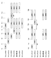
図1(A)は,画像フレームPFを示し,図1(B)は,画像フレームPFの画素Pの拡大図である。 FIG. 1A shows an image frame PF, and FIG. 1B is an enlarged view of a pixel P of the image frame PF.
図1(A)において,符号LNで示す1点鎖線は,画像が樽型に歪んでいる状態を模式的に示している。符号XはX軸を示し,符号YはY軸を示す。符号CNは,光学レンズの中心に対応する位置(X軸とY軸の交点)を示している。図1(A)において,画像フレームPF内の四角形により複数の画素を模式的に示している。符号dは,画素Pと中心CNとの距離を示す。 In FIG. 1 (A), a one-dot chain line indicated by a symbol LN schematically shows a state in which the image is distorted in a barrel shape. Symbol X indicates the X axis, and symbol Y indicates the Y axis. A symbol CN indicates a position corresponding to the center of the optical lens (intersection of X axis and Y axis). In FIG. 1 (A), a plurality of pixels are schematically shown by squares in the image frame PF. A symbol d indicates the distance between the pixel P and the center CN.
図1(B)において,縦線と横線(画素ライン)との交点部分を画素として示す。画素は,画素データ例えばRGBや,色差および輝度を有する。 In FIG. 1B, the intersection of the vertical line and the horizontal line (pixel line) is shown as a pixel. The pixel has pixel data such as RGB, color difference, and luminance.
図2の光学ディストーションカーブから明らかなように,画像フレームPFの中心CN付近では,光学歪みはあまり発生しないが,中心CNから画像フレーム辺部に向かうに従って,光学歪みが大きくなる。樽型歪みの場合には,画像フレームPFの中心CNから画像フレーム辺部に向かうに従って,光学歪み量が負の方向に大きくなる。なお,糸巻き型歪みの場合には,画像フレームPFの中心CNから画像フレーム辺部に向かうに従って,光学歪み量が正の方向に大きくなる。 As apparent from the optical distortion curve in FIG. 2, optical distortion does not occur much near the center CN of the image frame PF, but the optical distortion increases from the center CN toward the image frame side. In the case of barrel distortion, the amount of optical distortion increases in the negative direction from the center CN of the image frame PF toward the image frame side. In the case of pincushion distortion, the amount of optical distortion increases in the positive direction from the center CN of the image frame PF toward the image frame side.
この光学ディストーションカーブは,画像フレームPFの中心CNからの距離の多次元関数で近似的に算出できることが知られている。 It is known that this optical distortion curve can be approximately calculated by a multidimensional function of the distance from the center CN of the image frame PF.
この多次元関数の一例を(式1)に示す。 An example of this multidimensional function is shown in (Equation 1).
f(d)=α×d4+β×d2+γ…(式1)
(式1)において,dは図1に示した画像フレームPFの中心CNからの距離である。α,β,γは係数であり,例えば光学レンズの光学機器で定まる値である。
f (d) = α × d 4 + β × d 2 + γ (Equation 1)
In (Expression 1), d is the distance from the center CN of the image frame PF shown in FIG. α, β, and γ are coefficients, for example, values determined by the optical device of the optical lens.
図1に示した画像フレームPFにおいて,光学歪み補正対象の画素(以下,補正対象画素と記す)の座標をP(X,Y)とする。なお,ここでX,Yは整数値である。図1(B)において,補正対象画素Pを,黒色丸で示している。 In the image frame PF shown in FIG. 1, the coordinates of a pixel subject to optical distortion correction (hereinafter referred to as a correction target pixel) are P (X, Y). Here, X and Y are integer values. In FIG. 1B, the correction target pixel P is indicated by a black circle.
そして,この補正対象画素の画素データを補正するために必要となる光学歪み補正用画素の座標をp(x,y)とする。以下,光学歪み補正用画素の座標を補正用画素座標と記す。 The coordinates of the optical distortion correction pixel necessary for correcting the pixel data of the correction target pixel are defined as p (x, y). Hereinafter, the coordinates of the optical distortion correction pixel are referred to as correction pixel coordinates.
一般に,補正用画素座標p(x,y)は,(式2)を用いることにより算出できることが知られている。 In general, it is known that the pixel coordinates for correction p (x, y) can be calculated by using (Expression 2).
p(x,y)=(X×f(d),Y×f(d)); d=(X2+Y2)1/2…(式2)
画像フレームPFの光学歪みを補正する装置(以下,歪み補正装置と記す)は,補正対象画素Pの補正用画素座標p(x,y)を(式1),(式2)に基づき算出する。図1(B)において,補正用画素座標pを黒色4角で示す。
p (x, y) = (X × f (d), Y × f (d)); d = (X 2 + Y 2 ) 1/2 (Equation 2)
A device that corrects the optical distortion of the image frame PF (hereinafter referred to as a distortion correction device) calculates correction pixel coordinates p (x, y) of the correction target pixel P based on (Expression 1) and (Expression 2). . In FIG. 1B, the correction pixel coordinates p are indicated by black four corners.
歪み補正装置は,この補正用画素座標p(x,y)の近傍画素の画素データにより補間(算出)した画素データを補正対象画素Pの画素データとすることで光学歪みを補正する。 The distortion correction apparatus corrects the optical distortion by using pixel data interpolated (calculated) by pixel data of pixels near the correction pixel coordinate p (x, y) as pixel data of the correction target pixel P.
補間方法の一例として,補正用画素座標p(x,y)における近傍4画素Pa,Pb,Pc,Pdの画素データにより内挿補間する方法がある。この補間において,補正用画素座標p(x,y)とこの近傍4画素との距離に応じて重み係数を決定する。 As an example of the interpolation method, there is a method of performing interpolation using pixel data of four neighboring pixels Pa, Pb, Pc, and Pd in the correction pixel coordinates p (x, y). In this interpolation, a weighting coefficient is determined according to the distance between the correction pixel coordinates p (x, y) and the four neighboring pixels.
具体的には,補正用画素座標p(x,y)の整数部を(intx,inty)とし,小数部を(decx,decy)とすると,この補正用画素座標pの周囲にある近傍4画素の座標は,
Pa(intx,inty),Pb(intx,inty+1), Pc(intx+1,inty), Pd(intx+1,inty+1)である。
Specifically, if the integer part of the correction pixel coordinate p (x, y) is (intx, inty) and the decimal part is (decx, decy), four neighboring pixels around this correction pixel coordinate p The coordinates of
Pa (intx, inty), Pb (intx, inty + 1), Pc (intx + 1, inty), Pd (intx + 1, inty + 1).
ここで,補正対象画素Pの歪み補正画素データをPDD,近傍4画素Pa,Pb,Pc,Pdの画素データをそれぞれPad,Pbd,Pcd,Pddとする。 Here, it is assumed that the distortion correction pixel data of the correction target pixel P is PDD, and the pixel data of the four neighboring pixels Pa, Pb, Pc, and Pd are Pad, Pbd, Pcd, and Pdd, respectively.
この場合,補正対象画素Pの歪み補正画素データPDDは, (式3)に基づき,算出することができる。 In this case, the distortion correction pixel data PDD of the correction target pixel P can be calculated based on (Equation 3).
PDD=Pad×(1−decx)×(1−decy)+Pbd×(1−decx)×decy +Pcd×decx×(1−decy)+Pdd×decx×decy …(式3)
この歪み補正画素データPDDを補正対象画素Pの画素データとすることにより光学歪みを補正する。すなわち,補正前の補正対象画素Pの画素データを,この歪み補正画素データPDDに置き換える。
PDD = Pad x (1-decx) x (1-decy) + Pbd x (1-decx) x decy + Pcd x decx x (1-decy) + Pdd x decx x decy (Equation 3)
Optical distortion is corrected by using the distortion correction pixel data PDD as pixel data of the correction target pixel P. That is, the pixel data of the correction target pixel P before correction is replaced with the distortion correction pixel data PDD.
歪み補正装置は,画像フレームPFの全画素に対して以上説明した光学歪み補正処理を実行することにより,画像フレームPFの光学歪みを補正する。 The distortion correction apparatus corrects the optical distortion of the image frame PF by executing the above-described optical distortion correction processing for all the pixels of the image frame PF.
[立体画像生成装置]
図3は,本実施の形態の歪み補正装置を有する立体画像生成装置のブロック図の一例である。
[3D image generator]
FIG. 3 is an example of a block diagram of a stereoscopic image generation apparatus having the distortion correction apparatus of the present embodiment.
立体画像生成装置1のCPU10は,撮像装置11,画像プロセッサ12,操作部13,表示部14,第1のメモリ15,ROM16,記録部17,歪み補正装置18を制御,すなわち,立体画像生成装置1の全体を制御する。なお,上記各ブロックは,バスBを介して相互に接続されている。第1のメモリは,例えばフレームメモリであり,以下,第1のメモリ15をフレームメモリと記す。
The
撮像装置11は,第1の撮像部111と,第2の撮像部112とを有する。第1の撮像部111は,例えば,図示しない光学ユニットと,光学ユニットの光軸後方側に設けられた撮像素子,例えばCCD(Charge Coupled Device),CMOS(Complementary Metal Oxide Semiconductor)を有する。この光学ユニットは,例えば,被写体像を結像させる光学レンズと,この光学レンズを光軸方向に移動させて被写体像を示す入射光を撮像素子の受光面上に結像させる自動焦点調整機構(図示しない)と,A/Dコンバータ(図示しない)とを有する。A/Dコンバータは,撮像素子が出力するアナログの画像信号をデジタルの画像信号に変換する。画像プロセッサ12は,各種画像処理,例えばデジタルの画像信号にガンマ補正処理や,RGBデータを輝度データおよび色差データに変換するYC変換処理を実行して画像フレームを生成する。第1の撮像部111は,この構成により第1の画像フレームを生成する。
The imaging device 11 includes a
第2の撮像部112も第1の撮像部111と同様に,光学ユニット,撮像素子,A/Dコンバータを有する。そして,画像プロセッサ12は,前記したように,このA/Dコンバータが変換したデジタルの画像信号に各種画像処理を実行して画像フレームを生成する。第2の撮像部112は,この構成により第2の画像フレームを生成する。
Similarly to the
なお,画像プロセッサ12を撮像装置11と一体にしても良い。また,第1の画像フレームを左眼画像フレームとも言い,第2の画像フレームを右眼画像フレームとも言う。
The
第1の撮像部111の光軸と第2の撮像部112の光軸とのなす角度が輻輳角となるように,第1の撮像部111と第2の撮像部112とが配置されている。その結果,撮像装置11は,同一被写体について視差を有する第1,第2の画像フレームを生成することができる。
The
操作部13は,立体画像生成装置1を操作する機能を有し,例えば,電源ボタン,シャッター,操作ボタンを有する。
The
表示部14は,例えば,第1,第2の画像フレームや操作メニュー画面を表示する液晶パネル(図示しない)と,液晶パネルにおける表示処理を制御する制御部(図示しない)を有する。表示部14は,第1,第2の画像フレームにより立体視可能な画像を表示する。
The
フレームメモリ15は,第1の撮像部111,第2の撮像部112が生成した第1,第2の画像フレームや,後述する歪み補正処理が施された画像フレームを格納する。フレームメモリ15としては,例えば,SRAM(Static Random Access Memory),SDRAM(Synchronous Dynamic Random Access Memory)を利用できる。
The
ROM16は,例えば,各種パラメータや各種プログラムを格納する。
The
記録部17は,例えば着脱自在の記録媒体でも良く,例えば,第1の撮像部111,第2の撮像部112が生成した画像フレームを格納する。
The
[歪み補正装置の概略]
歪み補正装置18は,第1,第2の画像フレームの光学歪み補正処理を実行する。
[Outline of distortion correction device]
The
DMAコントローラ181は,歪み補正部183の制御に基づき,フレームメモリ15に格納された,同一被写体について視差を有する第1,第2の画像フレームの画素ラインの画素データをフレームメモリ15から読み出して第2のメモリ182に格納する読出部である。第2のメモリは,例えばラインメモリであり,以下,第2のメモリ182をラインメモリ182と記す。
Under the control of the
ラインメモリ182は,この画素ラインの画素データを格納する4ライン分のラインメモリP,Q,R,Sを有する。
The
ここで,4ライン分のラインメモリを設ける理由について説明する。(式3)で説明した光学歪み補正処理を実行する場合には,図2(B)の説明から明らかなように,2画素ラインの画素データを格納する2つのラインメモリが少なくとも必要である。 Here, the reason why the line memory for four lines is provided will be described. When executing the optical distortion correction processing described in (Equation 3), as is apparent from the description of FIG. 2B, at least two line memories for storing pixel data of two pixel lines are necessary.
しかし,2ライン分のラインメモリでは,この2つのラインメモリに格納された画素データにより光学歪み補正処理を実行している間に,新たな画素データをフレームメモリ15から読み出して,ラインメモリ182に格納することができない。その結果,光学歪み補正処理が遅延してしまう。そこで,2ライン分×2,すなわち4ライン分のラインメモリP,Q,R,Sを設けている。そのため,2つのラインメモリP,Qに格納された画素データにより光学歪み補正処理を実行している間に,新たな画素データをフレームメモリ15から読み出して,他のラインメモリR,Sに格納することができる。なお,4ライン以上のラインメモリを設けても良いが,ラインメモリの面積が大きくなる。そこで,本実施の形態では,4ライン分のラインメモリを設けた。
However, in the line memory for two lines, while executing the optical distortion correction process with the pixel data stored in the two line memories, new pixel data is read from the
歪み補正部183は,ラインメモリ182に格納された画素データにより第1,第2の画像フレームの光学歪み補正処理を行う。このとき,歪み補正部183は,第1,第2の画像フレームの光学歪み補正処理を第1の画像フレーム,次いで,第2の画像フレームの順に実行する。
The
歪み補正部183の算出部183aは,画像フレームにおける補正対象画素Pの補正用画素座標pを算出する座標算出部として動作する。この算出の際,算出部183aは,例えば,(式1),(式2)で示した所定の演算式に基づき,補正用画素座標pを算出する。さらに,算出部183aは,例えば,(式3)に基づき,ラインメモリ182に格納された画素データにより,補正対象画素Pの歪み補正画素データを算出する。
The
歪み補正部183は,算出部183aが算出した補正対象画素Pの歪み補正画素データをラインメモリ184に格納する。
The
ラインメモリ184は,歪み補正部183により光学歪みが補正された補正対象画素の画素データを格納する2ライン分のラインメモリV,Wを有する。ここで,2ライン分のラインメモリを設ける理由について説明する。光学歪みが補正された補正対象画素の画素データを格納する場合には,1ライン分のラインメモリを設ければ良い。しかし,1ライン分のラインメモリでは,光学歪みが補正された補正対象画素の画素データがこのラインメモリに格納されると,この画素データが読み出されるまで,新たな補正対象画素の画素データをラインメモリに格納することができなくなる。その結果,光学歪み補正処理が遅延してしまう。そこで,2ライン分のラインメモリを設けている。
The
DMAコントローラ185は,ラインメモリ184のラインメモリV,Wに格納された光学歪みが補正された画素データをフレームメモリ15に書き込む。
The DMA controller 185 writes the pixel data corrected for optical distortion stored in the line memories V and W of the
なお,座標格納メモリ186,アドレス算出部187については後述する。
The coordinate
[第1の画像フレームの光学歪み補正処理]
まず,図4〜図9に基づき,第1の画像フレームの光学歪み補正処理を説明する。
[Optical distortion correction processing for the first image frame]
First, the first image frame optical distortion correction processing will be described with reference to FIGS.
図4に示した画像フレームPFは,第1の撮像部111が生成した第1の画像フレームであり,フレームメモリ15に既に格納されている。
The image frame PF shown in FIG. 4 is a first image frame generated by the
また,図1(A)で説明したように,図4において,点線で示す四角形により,画像フレームPF内の複数の画素を模式的に示している。画像フレームPFの画素の座標と,この画像フレームPFがフレームメモリ15に格納されている場合における前記画素のフレームメモリ15におけるメモリアドレスとは対応している。
Further, as described with reference to FIG. 1A, in FIG. 4, a plurality of pixels in the image frame PF are schematically shown by squares indicated by dotted lines. The coordinates of the pixel of the image frame PF correspond to the memory address of the pixel in the
歪み補正部183は,例えば,画像フレームPFにおいて区分けされた4つの大ブロックI〜IVについて順次,光学歪み補正処理を実行する。図5に大ブロックIにおいて,最初に光学歪み補正処理を実行する画素ライン付近の拡大図を示す。この画素ラインは,図4に示した大ブロックIにおける上辺部近傍の画素ライン(図4の符号B0参照)である。なお,図4,図5において,説明のため画素や画素ラインを誇張して記載している。
For example, the
図6,図7のフロー図,図8のタイミングチャートにより第1の画像フレームの光学歪み補正処理の流れについて説明する。 The flow of the optical distortion correction process for the first image frame will be described with reference to the flowcharts of FIGS. 6 and 7 and the timing chart of FIG.
以下の説明において,歪み補正装置18は,例えば,6画素単位で光学歪み補正処理を実行する。以下,画素ラインにおいて,この6画素単位の画素から構成される画素ラインを単位画素ラインと記す。図5の例では,画素P0〜P5,画素P10〜P15,画素P20〜P25が単位画素ラインである。
In the following description, the
図6のステップS1:歪み補正部183は,DMAコントローラ181の初期設定を実行する。具体的には,歪み補正部183は,大ブロックにおいて最初の歪み補正対象画素ラインにおける単位画素ラインを補正するために用いる補正用画素データが格納されたフレームメモリ15におけるメモリアドレスをDMAコントローラ181に設定する。さらに,歪み補正部183は,このメモリアドレスに基づき読み出す画素データ量(以下,読み出し画素データ量と記す)と,読み出した画素データの転送後に移動する,フレームメモリ15におけるアドレス移動幅をDMAコントローラ181に設定する。読み出される画素データが格納されたフレームメモリ15の先頭アドレスとこのアドレス移動幅とを加算したメモリアドレス(オフセットアドレス)が,次回読み出される画素データが格納されているフレームメモリ15の先頭アドレスとなる。
Step S1:
図4に示した歪み補正対象の大ブロックIにおいて最初の歪み補正対象となる単位画素ラインは,図5に示した画素P0〜P5から構成される画素ラインである。 The unit pixel line that is the first distortion correction target in the large block I that is the distortion correction target illustrated in FIG. 4 is a pixel line that includes the pixels P0 to P5 illustrated in FIG.
この単位画素ラインの補正対象画素を補正するために必要な補正用画素データは,画素ラインL1の部分画素ラインR1の画素データ,画素ラインL2の部分画素ラインR2の画素データである。以下の説明では,図5の点線四角形で示す画素を部分画素ラインとして示す。 The correction pixel data necessary for correcting the correction target pixel of the unit pixel line is the pixel data of the partial pixel line R1 of the pixel line L1 and the pixel data of the partial pixel line R2 of the pixel line L2. In the following description, pixels indicated by dotted-line rectangles in FIG. 5 are shown as partial pixel lines.
補正対象画素P0〜P5はY軸近傍部分にあり,画像フレームの中心CNから余り離れておらず,光学歪みは相対的に大きくない。そのため,補正対象画素P0〜P5を有する画素ラインL0の近傍画素ラインである画素ラインL1の部分画素ラインR1,および,画素ラインL2の部分画素ラインR2の画素データが,補正対象画素P0〜P5を補正するために必要な補正用画素データとなる。 The correction target pixels P0 to P5 are in the vicinity of the Y axis, are not so far from the center CN of the image frame, and the optical distortion is not relatively large. Therefore, the pixel data of the partial pixel line R1 of the pixel line L1, which is a neighboring pixel line of the pixel line L0 having the correction target pixels P0 to P5, and the partial pixel line R2 of the pixel line L2 are changed to the correction target pixels P0 to P5. The pixel data for correction necessary for correction is obtained.
図6のステップS2: DMAコントローラ181は,前記設定されたフレームメモリ15のメモリアドレスにアクセスして,前記メモリアドレスに格納された画素データ(補正用画素データ)を読み出し,ラインメモリ182に転送,格納する。
Step S2 of FIG. 6: The
図5の例では,DMAコントローラ181は,フレームメモリ15において,部分画素ラインR1の画素データが格納されているメモリアドレスにアクセスして,この画素データをフレームメモリ15から読み出し,ラインメモリ182のラインメモリPに格納する(図8の時間T0〜T1における符号DW1)。そして,DMAコントローラ181は,フレームメモリ15において,部分画素ラインR2の画素データが格納されているメモリアドレスにアクセスして,この画素データをフレームメモリ15から読み出し,ラインメモリ182のラインメモリQに格納する(図8の時間T1〜T2における符号DW2)。
In the example of FIG. 5, the
図6のステップS3:算出部183aは,ステップS2で説明したDMAコントローラ181による補正用画素データのラインメモリ182への格納にあわせて,(式1),(式2)に基づき,補正対象画素の補正用画素座標を算出する。図5の例では,算出部183aは,(式1),(式2)に基づき,補正対象画素P0〜P5の補正用画素座標p0〜p5を算出する。
Step S3 in FIG. 6: The
図6のステップS4:歪み補正部183は,ラインメモリ182に格納された画素データだけで補正対象画素の歪み補正が可能か判定する。図5の例では,補正用画素座標p0〜p5の近傍4画素(部分画素ラインR1,R2)の画素データがラインメモリ182のラインメモリP,Qに格納されている。そのため,歪み補正部183は,ラインメモリ182に格納された画素データだけで補正対象画素の歪み補正が可能と判定する(ステップS4/YES)。
Step S4 in FIG. 6: The
図6のステップS5:歪み補正部183は,補正対象画素Pの座標(X,Y)と,(式1),(式2)に基づき算出された補正対象画素Pの補正用画素座標p(x,y)とが近似しているか判定する。ここで,補正対象画素Pの座標(X,Y)と,(式1),(式2)に基づき算出された補正対象画素Pの補正用画素座標p(x,y)とが近似しているとは,例えば,この補正対象画素Pの補正用画素の座標値の小数第1位を四捨五入した値が,補正対象画素Pの座標値と同値の場合である。ここでは,図5に示したように補正対象画素P0〜P5は画素ラインL0にあり,補正対象画素P0〜P5の補正用画素座標p0〜p5は,画素ラインL1,L2との間にある。すなわち,補正用画素座標p0〜p5の座標値の小数第1位を四捨五入した値が,補正対象画素P0〜P5の座標値と同値でなく,補正対象画素P0〜P5の座標と補正用画素座標p0〜p5とが近似しない。そのため,図7のステップS6に進む。
Step S5 in FIG. 6: The
図7のステップS6:算出部183aは,(式3)に基づき,ラインメモリ182に格納された画素データにより補正対象画素の歪み補正画素データを算出する。そして,歪み補正部183は,この歪み補正画素データをラインメモリ184に格納する。
Step S6 in FIG. 7: The
図5の例では,歪み補正部183は,ラインメモリPに格納された画素ラインL1の画素データを読み出す(図8の時間T2〜T4の符号DR1)。同じく,歪み補正部183は,ラインメモリQに格納された画素ラインL2の画素データを読み出す(図8の時間T2〜T4の符号DR2)。
In the example of FIG. 5, the
そして,算出部183aは,(式3)に基づき,補正対象画素P0〜P5の補正用画素座標p0〜p5の近傍4画素の画素データを有する前記読み出された画素データにより,補正対象画素P0〜P5の歪み補正画素データを算出し(図8の時間T2〜T4の符号AM1),算出した歪み補正画素データをラインメモリ184のラインメモリVに格納する(図8の時間T2〜T4の符号DW3)。
Based on (Equation 3), the
なお,DMAコントローラ185は,図8の時間T10〜T12における符号DR13に示すように,ラインメモリVに格納された補正対象画素P0〜P5の歪み補正画素データをラインメモリ184のラインメモリVから読み出す。そして,DMAコントローラ185は,フレームメモリ15において光学歪み補正後の第1の画像フレームが格納される領域に,補正対象画素P0〜P5の座標と対応させて補正対象画素P0〜P5の歪み補正画素データを格納する。
Note that the DMA controller 185 reads the distortion correction pixel data of the correction target pixels P0 to P5 stored in the line memory V from the line memory V of the
このように,DMAコントローラ185は,随時,歪み補正部183により算出された補正対象画素の歪み補正画素データをラインメモリ184から読み出す。そして,DMAコントローラ185は,フレームメモリ15において光学歪み補正後の第1の画像フレームが格納される領域に,補正対象画素の座標と対応させて,補正対象画素の歪み補正画素データを格納する。以下,この処理の内容については説明を省略する。
As described above, the DMA controller 185 reads the distortion correction pixel data of the correction target pixel calculated by the
ステップS3〜S6の処理に並行して,現在の補正対象である単位画素ラインの次の単位画素ラインにおける画素P10〜P15(図5参照)の歪み補正処理を行うため,図8の時間T2〜T4の間に,下記の画素データ転送処理が実行される。 In parallel with the processing of steps S3 to S6, in order to perform the distortion correction processing of the pixels P10 to P15 (see FIG. 5) in the next unit pixel line of the unit pixel line that is the current correction target, The following pixel data transfer process is executed during T4.
すなわち,DMAコントローラ181は,ステップS2で設定されたメモリアドレス,読み出し画素データ量,アドレス移動幅に基づき,フレームメモリ15から補正対象画素P10〜P15の補正用画素データを新たに読み出し,ラインメモリ182の空き領域に格納する。
That is, the
図5の例では,DMAコントローラ181は,フレームメモリ15において,画素ラインL1の部分画素ラインR3の画素データが格納されているメモリアドレスにアクセスして,この画素データを読み出しラインメモリRに格納する(図8の時間T2〜T3における符号DW4)。さらに,DMAコントローラ181は,フレームメモリ15において,図5に示した画素ラインL2の部分画素ラインR4の画素データが格納されているメモリアドレスにアクセスして,この画素データを読み出しラインメモリSに格納する(図8の時間T3〜T4における符号DW5)。この画素データの読み出し格納処理は,ステップS2で実行される処理である。
In the example of FIG. 5, the
歪み補正部183は,フレームメモリ15から読み出された画素データにより,補正対象画素の歪み補正を実行すると共に,図7のステップS7を実行する。
The
図7のステップS7:歪み補正部183は,大ブロックにおける1画素ラインの全画素の歪み補正処理が終了したか判定する。ここではまだ,終了していないので(ステップS7/NO),図6のステップS2に移る。DMAコントローラ181は,前記したように,次の補正対象画素の補正用画素データを同一画素ラインにおいて順次読み出す(図8の時間T2〜T4の符号DW4,DW5参照)。
Step S7 in FIG. 7: The
次に,算出部183aは,(式1),(式2)に基づき,補正対象画素P10〜P15の補正用画素座標p10〜p15を算出する(図6のステップS3)。
Next, the
さて,図5に示したように,補正対象画素P10〜P12については,補正用画素座標p10〜p12が画素ラインL1と画素ラインL2との間にある。そして,補正対象画素P10〜P12の補正用画素データを有する補正用画素データ(図5の部分画素ラインR3,R4の画素データ)は,既にラインメモリR,Sに格納されている。そのため,歪み補正部183は,補正対象画素P10〜P12については,この補正用画素データにより歪み補正処理が可能である(図6のステップS4/YES)。
Now, as shown in FIG. 5, for the correction target pixels P10 to P12, the correction pixel coordinates p10 to p12 are between the pixel line L1 and the pixel line L2. And the correction pixel data (pixel data of the partial pixel lines R3 and R4 in FIG. 5) having the correction pixel data of the correction target pixels P10 to P12 are already stored in the line memories R and S. Therefore, the
そこで,歪み補正部183は,ラインメモリRに格納された部分画素ラインR3の画素データを読み出す(図8の時間T10〜T12の符号DR11)。さらに,歪み補正部183は,ラインメモリSに格納された部分画素ラインR4の画素データを読み出す(図8の時間T10〜T12の符号DR12)。
Therefore, the
そして,算出部183aは,(式3)に基づき,この読み出された画素データにより補正対象画素P10〜P12の歪み補正画素データを算出する(図8の時間T10〜T12の符号AM12)。そして,歪み補正部183は,この歪み補正画素データをラインメモリWに書き込む(図8の時間T10〜T12の符号DW11)。
Based on (Equation 3), the
しかし,補正対象画素P13〜P15については,補正対象画素P13〜P15の補正用画素データはラインメモリR,Sに格納されていないので,補正対象画素P10〜P12のように歪み補正処理を実行することができない(図6のステップS4/NO)。換言すれば,図5に示したように,補正対象画素P13〜P15の補正用画素座標p13〜p15が画素ラインL2と画素ラインL3との間にある。 However, for the correction target pixels P13 to P15, since the correction pixel data of the correction target pixels P13 to P15 is not stored in the line memories R and S, the distortion correction processing is executed like the correction target pixels P10 to P12. (Step S4 / NO in FIG. 6). In other words, as shown in FIG. 5, the correction pixel coordinates p13 to p15 of the correction target pixels P13 to P15 are between the pixel line L2 and the pixel line L3.
そのため,補正対象画素P13〜P15の歪み補正処理を実行するためには,画素ラインL3における補正用画素座標p13〜p15の近傍画素(図5の部分画素ラインR11)の画素データが必要になる。なお,画素ラインL2における補正用画素座標p13〜p15の近傍画素(図5の部分画素ラインR12)の画素データは,既に,ラインメモリSに格納されている。 Therefore, in order to execute the distortion correction processing of the correction target pixels P13 to P15, pixel data of pixels near the correction pixel coordinates p13 to p15 (partial pixel line R11 in FIG. 5) in the pixel line L3 is necessary. Note that pixel data of pixels near the correction pixel coordinates p13 to p15 (partial pixel line R12 in FIG. 5) in the pixel line L2 is already stored in the line memory S.
以上説明したように,補正対象画素P13〜P15の歪み補正を実行する場合には,図6のステップS4でNOとなり,図6のステップS8に移る。 As described above, when the distortion correction of the correction target pixels P13 to P15 is executed, NO is determined in step S4 in FIG. 6, and the process proceeds to step S8 in FIG.
図6のステップS8:歪み補正装置18は,メモリチェンジ処理を実行し補正用画素データをフレームメモリ15から新たに読み出す。
Step S8 in FIG. 6: The
図5の例では,まず,歪み補正部183は,補正用画素座標p13〜p15に基づき,補正対象画素P13〜P15の補正用画素データが格納されたフレームメモリ15におけるメモリアドレスを算出する。具体的には,フレームメモリ15において,画素ラインL3における補正用画素座標p13〜p15の近傍画素(図5の部分画素ラインR11)の画素データが格納されているメモリアドレスである。
In the example of FIG. 5, the
そして,歪み補正部183は,このメモリアドレスをDMAコントローラ181に出力する。DMAコントローラ181は,このメモリアドレス入力に応答して,フレームメモリ15からこのメモリアドレスに対応する補正対象画素P13〜P15の補正用画素データを読み出し,ラインメモリ182のラインメモリRに格納する(図8の時間T12〜T13の符号DW12)。
Then, the
このように,ラインメモリ182に格納された画素データにより,画像フレームにおける補正対象画素の光学歪み補正処理を実行できない場合,フレームメモリ15から新たに補正用画素データを読み出す処理をメモリチェンジと呼ぶ。このメモリチェンジ処理により,画像フレームの光学歪み補正時間が長くなる。このメモリチェンジの時間を図8の符号MCで示す。
In this way, when the pixel data stored in the
特に,第1の画像フレームに続いて,第2の画像フレームの光学歪み補正処理を実行する場合,メモリチェンジ処理にかかる時間を削減する必要がある。そこで,第1の画像フレームの光学歪み補正処理において,図6のステップS9の処理を行う。 In particular, when the optical distortion correction process for the second image frame is executed following the first image frame, it is necessary to reduce the time required for the memory change process. Therefore, the process of step S9 in FIG. 6 is performed in the optical distortion correction process of the first image frame.
図6のステップS9:歪み補正部183は,メモリチェンジが発生する際に歪み補正処理を実行していた補正対象画素の補正用画素座標をメモリチェンジ座標として第3のメモリ186に格納する。第3のメモリは,座標格納メモリであり,以下,第3のメモリ186を座標格納メモリ186と記す。
Step S9 in FIG. 6: The
図5の例では,歪み補正部183は,補正用画素座標p13をメモリチェンジ座標p13として座標格納メモリ186に格納する。なお,メモリチェンジ座標として,座標p13〜p15を格納してもよい。
In the example of FIG. 5, the
すなわち,歪み補正部183は,第1の画像フレームの光学歪み補正処理を実行する過程において,ラインメモリ182に格納された画素データにより,第1の画像フレームにおける補正対象画素の光学歪み補正処理を実行できない場合,光学歪み補正処理を実行できない補正対象画素に係る第1の座標情報として,例えば,光学歪み補正処理を実行できない補正対象画素の補正用画素座標(メモリチェンジ座標)を座標格納メモリ186に格納する。
That is, the
このメモリチェンジ座標を格納する理由について説明する。図1,図2で説明した(式1)における係数α,β,γは,(式1)で説明したように,光学機器固有の値である。そして,第1の画像フレームを生成する第1の撮像部111と,第2の画像フレームを生成する第2の撮像部112は同一の光学機器を使用しているため,第1の画像フレームの光学歪み補正処理を実行する場合の(式1)における係数α,β,γと,第2の画像フレームの光学歪み補正処理を実行する場合の(式1)における係数α,β,γとは実質的に同値である。
The reason for storing the memory change coordinates will be described. The coefficients α, β, and γ in (Equation 1) described with reference to FIGS. 1 and 2 are values unique to the optical device as described in (Equation 1). Since the
第1,第2の画像フレームの縦横画素数が同一,中心座標が同一の場合を想定する。この場合,第1の画像フレームにおける補正対象画素座標P(X,Y)と第2の画像フレームにおける補正対象画素座標P'(X',Y')が同値であれば,第1の画像フレームにおける補正対象画素Pの補正用画素座標p(x,y)と,第2の画像フレームにおける補正対象画素P'の補正用画素座標p'(x',y')とは同値である。そして,第1,第2の画像フレームの縦横画素数は同一,中心座標は同一である。 Assume that the first and second image frames have the same number of vertical and horizontal pixels and the same center coordinates. In this case, if the correction target pixel coordinates P (X, Y) in the first image frame and the correction target pixel coordinates P ′ (X ′, Y ′) in the second image frame are the same value, the first image frame The correction pixel coordinate p (x, y) of the correction target pixel P in FIG. 5 and the correction pixel coordinate p ′ (x ′, y ′) of the correction target pixel P ′ in the second image frame have the same value. The first and second image frames have the same number of vertical and horizontal pixels and the same center coordinates.
とすれば,第1の画像フレームにおいて,ラインメモリ182に格納された画素データにより光学歪み補正処理を実行できない補正対象画素の補正用画素座標,すなわちメモリチェンジが発生する補正対象画素の補正用画素座標と,第2の画像フレームにおいて,ラインメモリ182に格納された画素データにより光学歪み補正処理を実行できない補正対象画素の補正用画素座標とは同値になる。
Then, in the first image frame, the correction pixel coordinates of the correction target pixel that cannot be subjected to the optical distortion correction processing by the pixel data stored in the
そのため,第1の画像フレームにおいて光学歪み補正処理を実行できない補正対象画素,または,この補正対象画素の補正用画素座標を利用すれば,第2の画像フレームの光学歪み補正処理において,メモリチェンジが発生するタイミングを予測することできる。このタイミングを予測できれば,第2の画像フレームの光学歪み補正処理において,メモリチェンジが発生する補正対象画素の補正用画素データを予めラインメモリ182に格納(プリフェッチとも言う)することができる。その結果,第2の画像フレームの光学歪み補正処理において,メモリチェンジに必要な時間を削減することができる。
Therefore, if a correction target pixel that cannot be subjected to the optical distortion correction process in the first image frame or a correction pixel coordinate of the correction target pixel is used, a memory change is caused in the optical distortion correction process of the second image frame. The timing of occurrence can be predicted. If this timing can be predicted, the correction pixel data of the correction target pixel in which the memory change occurs can be stored in the
そこで,歪み補正部183は,第1の画像フレームの歪み補正処理を実行する過程において,ラインメモリ182に格納された画素データにより,第1の画像フレームにおける補正対象画素の光学歪み補正処理を実行できない場合,すなわちメモリチェンジが発生する場合,図6のステップS9で説明した処理を実行する。歪み補正部183は,ステップS9において,この光学歪み補正処理を実行できない補正対象画素に係る座標情報を座標格納メモリ186に格納する。
Therefore, the
ステップS9の終了後,図7のステップS6で説明したように,歪み補正部183は,補正対象画素P13〜P15の歪み補正処理を実行するため,ラインメモリR,Sに格納された画素データを読み出す(図8の時間T13〜T14の符号DR14,DR15)。
After the completion of step S9, as described in step S6 of FIG. 7, the
そして,算出部183aは,(式3)に基づき,この読み出された画素データにより補正対象画素P13〜P15の歪み補正画素データを算出する(図8の時間T13〜T14の符号AM13)。そして,歪み補正部183は,この歪み補正画素データをラインメモリ184のラインメモリVに格納する(図8の時間T13〜T14の符号DW13)。
Based on (Equation 3), the
すなわち,図6のステップS8において,歪み補正部183は,光学歪み補正処理を実行できない補正対象画素の補正用画素データをラインメモリ182に格納するようにDMAコントローラ181を制御する。そして,図7のステップS6において,算出部183aは,(式3)に基づき,ラインメモリ182に格納された画素データにより,前記補正対象画素の歪み補正画素データを算出する。
That is, in step S8 of FIG. 6, the
さて,現在の補正対象である単位画素ラインの次の単位画素ラインにおける画素P20〜P25(図5参照)の歪み補正処理を行うため,図8の時間T10〜T12の間に,下記の画素データ転送処理が実行される。すなわち,図6のステップS2で説明したように,DMAコントローラ181は,図5の例では,フレームメモリ15において,部分画素ラインR21の画素データが格納されているメモリアドレスにアクセスして,この画素データをフレームメモリ15から読み出しラインメモリPに格納する(図8の時間T10〜T11における符号DW14)。さらに,DMAコントローラ181は,フレームメモリ15において,部分画素ラインR22の画素データが格納されているメモリアドレスにアクセスして,この画素データをフレームメモリ15から読み出しラインメモリQに格納する(図8の時間T11〜T12における符号DW15)。
Now, in order to perform distortion correction processing of the pixels P20 to P25 (see FIG. 5) in the unit pixel line next to the unit pixel line that is the current correction target, the following pixel data is used during the time T10 to T12 in FIG. The transfer process is executed. That is, as described in step S2 of FIG. 6, in the example of FIG. 5, the
なお,歪み補正部183は,上記メモリチェンジを実行した場合には,以後,読み出し先のラインをメモリチェンジ後の画素ラインに切り替えてもよい。例えば,図5の例では,歪み補正部183は,読み出し先のラインを画素ラインL1から画素ラインL3に切り換えるようにDMAコントローラ181に指示する。以後,DMAコントローラ181は,画素ラインL2と画素ラインL3から画素データを読み出すことになる。その結果,メモリチェンジの発生頻度が低下する。
If the memory change is executed, the
次に,図6のステップS3で説明したように,歪み補正部183は,補正対象画素P20〜P25の補正用画素座標p20〜p25の算出を実行する。
Next, as described in step S3 of FIG. 6, the
しかし,補正対象画素P20〜P25の補正用画素データはラインメモリP,Qに格納されていないので,歪み補正処理を実行することができない(図6のステップS4/NO)。これは,前記したように,光学歪みが大きくなり,前回読み出した画素ラインL1,L2の画素データでは光学歪み補正ができないからである。 However, since the correction pixel data of the correction target pixels P20 to P25 is not stored in the line memories P and Q, the distortion correction process cannot be executed (step S4 / NO in FIG. 6). This is because, as described above, the optical distortion increases, and the optical distortion correction cannot be performed with the pixel data of the pixel lines L1 and L2 read out last time.
そこで,図6のステップS8で説明したように,歪み補正部183は,DMAコントローラ181により,図5に示した画素ラインL3における補正用画素座標p20〜p22の近傍画素(図5の部分画素ラインR31)の画素データをフレームメモリ15から読み出しラインメモリPに格納する(図8の時間T20〜T21の符号DW21)。さらに,歪み補正部183は,DMAコントローラ181により,画素ラインL4における補正用画素座標p20〜p22の近傍画素(図5の部分画素ラインR32)の画素データをフレームメモリ15から読み出しラインメモリQに格納する(図8の時間T21〜T22の符号DW22)。
Therefore, as described in step S8 in FIG. 6, the
歪み補正部183は,図6のステップS9で説明したように,ラインメモリ182に格納された画素データにより,第1の画像フレームにおける補正対象画素の光学歪み補正処理を実行できない場合,この補正対象画素の補正用画素座標をメモリチェンジ座標として座標格納メモリ186に格納する。図5の例では,歪み補正部183は,補正用画素座標p20をメモリチェンジ座標p20として座標格納メモリ186に格納する。なお,メモリチェンジ座標として,座標p20〜p22を格納してもよい。
As described in step S9 of FIG. 6, the
そして,歪み補正部183は,図7のステップS6で説明したように,ラインメモリ182のラインメモリP,Qに格納された画素データを読み出す(図8の時間T22〜T23の符号DR21,DR22)。また,算出部183aは,(式3)に基づき,この読み出された画素データにより補正対象画素P20〜P22の歪み補正画素データを算出する(図8の時間T22〜T23の符号AM21)。そして,歪み補正部183は,算出した歪み補正画素データをラインメモリ184のラインメモリVに格納する(図8の時間T22〜T23の符号DW23)。
Then, as described in step S6 of FIG. 7, the
さらに,補正対象画素P23〜P25の歪み補正処理を実行するために,歪み補正部183は,DMAコントローラ181により,画素ラインL5における補正用画素座標p23〜p25の近傍画素(図5の部分画素ラインR33)の画素データをフレームメモリ15から読み出しラインメモリPに格納する(図8の時間T23〜T24の符号DW24)。さらに,歪み補正部183は,DMAコントローラ181により,画素ラインL6における補正用画素座標p23〜p25の近傍画素(図5の部分画素ラインR34)の画素データをフレームメモリ15から読み出しラインメモリQに格納する(図8の時間T24〜T25の符号DW25)。
Further, in order to execute the distortion correction processing of the correction target pixels P23 to P25, the
歪み補正部183は,図6のステップS9で説明したように,ラインメモリ182に格納された画素データにより,第1の画像フレームにおける補正対象画素の光学歪み補正処理を実行できない場合,この補正対象画素の補正用画素座標をメモリチェンジ座標として座標格納メモリ186に格納する。図5の例では,歪み補正部183は,補正用画素座標p23をメモリチェンジ座標p23として座標格納メモリ186に格納する。なお,メモリチェンジ座標として,座標p23〜p25を格納してもよい。
As described in step S9 of FIG. 6, the
そして,歪み補正部183は,図7のステップS6で説明したように,ラインメモリ182のラインメモリP,Qに格納された画素データを読み出す(図8の時間T25〜T26の符号DR23,DR24)。また,算出部183aは,(式3)に基づき,この読み出された画素データにより補正対象画素P23〜P25の歪み補正画素データを算出する(図8の時間T25〜T26の符号AM22)。そして,歪み補正部183は,算出した歪み補正画素データをラインメモリ184のラインメモリVに格納する(図8の時間T25〜T26の符号DW26)。
Then, as described in step S6 of FIG. 7, the
補正対象画素P20〜P25の歪み補正処理が終了すると,図7のステップS7に移る。 When the distortion correction processing for the correction target pixels P20 to P25 ends, the process proceeds to step S7 in FIG.
以上説明したように,図6のステップS2〜ステップS9の処理を繰り返し行い,画素ラインL0の全画素の歪み補正処理が終了したとする。すると,図7のステップS7において,大ブロックにおける1画素ラインの全画素の歪み補正処理が終了したと判定(ステップS7/YES)されるので,図7のステップS10に移る。 As described above, it is assumed that the processing in steps S2 to S9 in FIG. 6 is repeatedly performed and the distortion correction processing for all the pixels in the pixel line L0 is completed. Then, in step S7 in FIG. 7, since it is determined that the distortion correction processing for all the pixels of one pixel line in the large block is completed (step S7 / YES), the process proceeds to step S10 in FIG.
図7のステップS10: 歪み補正部183は,図4に示した1つの大ブロックの光学歪み補正処理が終了したか判定する。ここでは,まだ,1つの大ブロックの光学歪み補正処理が終了していないので(ステップS10/NO),図6のステップS2に戻る。図6のステップS2において,歪み補正部183は,歪み補正対象の大ブロックにおいて,現在の補正対象の画素ラインL0の次の画素ラインL1における単位画素ラインを補正するために必要な画素データが格納されたフレームメモリ15におけるメモリアドレスなどをDMAコントローラ181に設定する。
Step S10 in FIG. 7: The
そして,歪み補正装置18は,図6のステップS2〜図7のステップS10の処理を繰り返し行い,図4の符号A12に示すように,画素ラインL1,L2…と補正対象画素ラインを順次移動させて画素ラインの光学歪み補正処理を実行する。すると,図9に示すように,図4の大ブロックIにおける中心CN近傍の画素ラインにおける画素の歪み補正処理を実行することになる。
Then, the
図9は,図4の大ブロックIにおける中心CN近傍の画素配列(図4の符号Bn0参照)を模式的に示した図である。 FIG. 9 is a diagram schematically illustrating a pixel array (see reference sign Bn0 in FIG. 4) in the vicinity of the center CN in the large block I in FIG.
ここで,画素P100〜P105が補正対象画素であるとする。そして,図6のステップS2の処理により,既に,この補正対象画素P100〜P105の補正用画素データがラインメモリ182に格納されているとする。この状態で,歪み補正部183は,補正対象画素P100〜P105の補正用画素座標p100〜p105を算出する(図6のステップS3)。そして,図6のステップS4に移る。ここで,ラインメモリ182に格納された補正用画素データだけで補正対象画素P100〜P105の歪み補正処理が可能なので(ステップS4/YES),ステップS5に移る。
Here, it is assumed that the pixels P100 to P105 are correction target pixels. Then, it is assumed that the correction pixel data of the correction target pixels P100 to P105 is already stored in the
歪み補正部183は,補正対象画素Pの座標(X,Y)と,補正対象画素Pの補正用画素座標p(x,y)とが近似しているか判定する(ステップS5)。
The
さて,図9に示したように,大ブロックIにおける中心CN近傍の画素ラインの画素の歪み補正処理を行う場合,補正対象画素の座標と,この補正対象画素の補正用画素座標とが近似する。ここで,補正対象画素の座標と,この補正対象画素の補正用画素座標とが近似する第1の例としては,前記したように,この補正対象画素の補正用画素の座標値の小数第1位を四捨五入した値が,この補正対象画素の座標値と同値の場合がある。補正対象画素の座標と,この補正対象画素の補正用画素座標とが近似する第2の例としては,例えば,補正対象画素の座標値と,この補正対象画素の補正用画素の座標値との差が,所定の値(例えば,0.3)未満である場合がある。 Now, as shown in FIG. 9, when the distortion correction processing is performed on the pixels in the pixel line near the center CN in the large block I, the coordinates of the correction target pixel approximate to the correction pixel coordinates of the correction target pixel. . Here, as described above, as a first example in which the coordinates of the correction target pixel and the correction pixel coordinates of the correction target pixel are approximated, as described above, the first decimal value of the correction pixel coordinate value of the correction target pixel is used. The value rounded off to the right may be the same value as the coordinate value of the correction target pixel. As a second example in which the coordinates of the correction target pixel and the correction pixel coordinates of the correction target pixel are approximated, for example, the coordinate value of the correction target pixel and the coordinate value of the correction pixel of the correction target pixel are The difference may be less than a predetermined value (eg, 0.3).
なお,座標値とは,X座標値およびY座標値であってもよいし,X座標値またはY座標値の何れか1つであってもよい。 The coordinate value may be an X coordinate value and a Y coordinate value, or may be either one of an X coordinate value or a Y coordinate value.
このように,補正対象画素の座標と,補正用画素座標とが近似するのは,画像フレームの中心CN付近では光学歪みが殆ど発生しないからである。 As described above, the coordinates of the correction target pixel and the correction pixel coordinate approximate to each other because optical distortion hardly occurs in the vicinity of the center CN of the image frame.
補正対象画素の座標と,補正用画素座標とが近似する場合(図6のステップS5/YES),図7のステップS11に移る。 When the coordinates of the correction target pixel and the correction pixel coordinates are approximate (step S5 / YES in FIG. 6), the process proceeds to step S11 in FIG.
図7のステップS11:歪み補正部183は,この補正用画素座標をスルー座標として座標格納メモリ186に格納する。
Step S11 in FIG. 7: The
すなわち,歪み補正部183は,第1の画像フレームの光学歪み補正処理を実行する過程において,第1の画像フレームにおける補正対象画素の座標とこの補正対象画素の補正用画素座標とが近似する場合,この補正対象画素に係る座標情報を座標格納メモリ186に格納する。この座標情報は,例えば,この近似する補正対象画素の補正用画素座標(スルー座標)である。
That is, in the process of executing the optical distortion correction processing for the first image frame, the
そして,歪み補正部183は,図10〜図12で説明する第2の画像フレームの光学歪み補正処理を実行する過程において,座標格納メモリ186に格納された近似する補正対象画素に係る座標情報に基づき,この近似する補正対象画素に対応する,第2の画像フレームにおける補正対象画素の光学歪み補正処理を実行するか否かを決定する。
Then, the
図9の例では,歪み補正部183は,補正用画素座標p100〜p105をスルー座標p100〜p105として座標格納メモリ186に格納する。なお,スルー座標が同値の場合,その中の1つの目の座標のみをスルー座標として座標格納メモリ186に格納しても良い。例えば,補正用画素座標p100〜p105が同値の場合,座標p100のみをスルー座標として座標格納メモリ186に格納する。
In the example of FIG. 9, the
以後,歪み補正部183が,上記説明した光学歪み補正処理を実行し,図4に示した大ブロックIの光学歪み補正処理が終了すると(図7のステップS10/YES),図7のステップS12に移る。
Thereafter, when the
図7のステップS12:歪み補正部183は,全大ブロックの光学歪み補正処理が終了したか判定する。ここでは,大ブロックIの光学歪み補正処理が終了しただけなので(ステップS12/NO),ステップS1に戻る。図6のステップS1において,歪み補正部183は,現在の歪み補正対象の大ブロックIの次の歪み補正対象ブロックIIにおいて,最初の単位画素ラインを補正するために必要な画素データが格納されたフレームメモリ15におけるメモリアドレスなどをDMAコントローラ181に設定する。
Step S12 in FIG. 7: The
以後,歪み補正部183は,図6ステップS1〜図7のステップS12の処理を繰り返し行い,図4の画像フレームPFにおける大ブロックII,III,IVの光学歪み補正処理を順次実行する。なお,歪み補正部183は,大ブロックII,III,IVの歪み補正処理においては,1画素ラインの歪み補正処理を図4の矢印A21,A31,A41方向に実行する。そして,歪み補正部183は,この1画素ラインの歪み補正処理が終了すると矢印A22,A32,A42方向に向けて補正対象の画素ラインを移動させて歪み補正処理を実行する。
Thereafter, the
図4〜図9で説明した歪み補正処理により第1の画像フレームPFの歪み補正処理が終了すると(図7のステップS12/YES),歪み補正装置18は,第1の画像フレームにおける同一被写体について視差を有する第2の画像フレームの歪み補正処理を実行することになる。
When the distortion correction processing of the first image frame PF is completed by the distortion correction processing described with reference to FIGS. 4 to 9 (step S12 / YES in FIG. 7), the
[第2の画像フレームの光学歪み補正処理]
第1の画像フレームの光学歪み補正処理終了後,歪み補正部183は,第2の画像フレームの光学歪み補正処理を実行する。歪み補正部183は,第2の画像フレームの光学歪み補正処理を実行する過程において,座標格納メモリ186に格納された光学歪み補正処理を実行できない補正対象画素に係る座標情報(メモリチェンジ座標)に基づき,この光学歪み補正処理を実行できない補正対象画素に対応する,第2の画像フレームにおける補正対象画素の補正用画素データをラインメモリ182に格納するようにDMAコントローラ181を制御する。すなわち,補正用画素データをプリフェッチする。このプリフェッチにより,光学歪み補正処理を高速化できる。
[Second image frame optical distortion correction processing]
After completion of the optical distortion correction process for the first image frame, the
そして,算出部183aは,(式3)に基づき,ラインメモリ182に格納された画素データにより,第2の画像フレームにおける補正対象画素の歪み補正画素データを算出する。
Based on (Equation 3), the
さらに,歪み補正部183は,第2の画像フレームの光学歪み補正処理を実行する過程において,座標格納メモリ186に格納された近似する補正対象画素に係る座標情報(スルー座標)に基づき,この近似する補正対象画素に対応する,第2の画像フレームにおける補正対象画素の光学歪み補正処理を実行するか否かを決定する。この決定処理により,不要な光学歪み補正処理を実行しないので,光学歪み補正処理を高速化できる。
Further, the
第2の画像フレームの歪み補正処理の詳細について,図10〜図12に基づき説明する。 Details of the distortion correction processing of the second image frame will be described with reference to FIGS.
第2の画像フレームの歪み補正処理を実行する場合においても,歪み補正装置18は,6画素単位で光学歪み補正処理を実行する。また,歪み補正装置18は,最初に大ブロックIに対して歪み補正を実行する。なお,第2の画像フレームは,既に,フレームメモリ15に格納されているとする。
Even when the distortion correction processing of the second image frame is executed, the
また,第2の画像フレームは,図4,図5で説明した第1の画像フレームに対応する。具体的に説明すると,第1,第2の画像フレームの縦横画素数が同一であり,中心座標が同一である。そのため,第1の画像フレームにおける補正対象画素座標P(X,Y)と第2の画像フレームにおける補正対象画素座標P'(X',Y')が同値の場合,第1の画像フレームにおける補正対象画素Pの補正用画素座標p(x,y)と,第2の画像フレームにおける補正対象画素P'の補正用画素座標p'(x',y')とは同値になる。 The second image frame corresponds to the first image frame described with reference to FIGS. More specifically, the first and second image frames have the same number of vertical and horizontal pixels and the same center coordinates. Therefore, when the correction target pixel coordinate P (X, Y) in the first image frame and the correction target pixel coordinate P ′ (X ′, Y ′) in the second image frame are the same value, the correction in the first image frame is performed. The correction pixel coordinates p (x, y) of the target pixel P and the correction pixel coordinates p ′ (x ′, y ′) of the correction target pixel P ′ in the second image frame have the same value.
図10のステップS21:図6のステップS1と同様に,歪み補正部183は,DMAコントローラ181の初期設定を実行する。第2の画像フレームの光学歪み補正処理においても,第1の画像フレームと同様に,図4に示した歪み補正対象の大ブロックIにおいて最初の歪み補正対象となる単位画素ラインは,図5に示した画素P0〜P5である。
Step S21 in FIG. 10: As with step S1 in FIG. 6, the
図10のステップS22:歪み補正部183は,座標格納メモリ186に格納された座標を順次読み出す(図12の時間T30〜T31における符号MR31)。座標格納メモリ186には,図6で説明したようにメモリチェンジ座標p13,p20,p23が格納され,スルー座標p100が格納されている。なお,座標格納メモリ186に格納された全メモリチェンジ座標を一度に読み出してもよい。同じく,座標格納メモリ186に格納された全スルー座標を一度に読み出してもよい。
Step S22 in FIG. 10: The
図10のステップS23:算出部183aは,(式1),(式2)に基づき,補正対象画素の補正用画素座標を算出する。図5の場合,補正対象画素P0〜P5の補正用画素座標p0〜p5を算出する。
Step S23 in FIG. 10: The calculating
図10のステップS24:歪み補正部183は,補正対象画素の歪み補正処理をするために,メモリチェンジする必要があるか判定する。具体的には,歪み補正部183は,算出した補正用画素座標と,座標格納メモリ186から読み出したメモリチェンジ座標とが一致する場合には,メモリチェンジする必要があると判定する。補正用画素座標p0〜p5の場合,補正用画素座標p0〜p5と同じメモリチェンジ座標は,座標格納メモリ186に格納されていない(座標格納メモリ186から読み出されていない)ので,ステップS24では不一致(ステップS24/NO)となり,図10のステップS25に移る。
Step S24 in FIG. 10: The
図10のステップS25:歪み補正部183は,補正対象画素の歪み補正処理をスルー,すなわち,補正対象画素の歪み補正処理を実行しないか判定する。具体的には,歪み補正部183は,補正対象画素の補正用画素座標とスルー座標とが一致するか判定する。補正用画素座標p0〜p5の場合,補正用画素座標p0〜p5と同じスルー座標は,座標格納メモリ186に格納されていない(座標格納メモリ186から読み出されていない)ので,ステップS25では不一致(ステップS25/NO)となり,図10のステップS26に移る。
Step S25 in FIG. 10: The
図10のステップS26:歪み補正部183は,算出した補正用画素座標p0〜p5に基づき,補正対象画素P0〜P5の歪み補正画素データが格納された非メモリチェンジ用のアドレスを算出する。
Step S26 in FIG. 10: The
具体的には,歪み補正部183は,フレームメモリ15において,図5の画素ラインL1,L2における補正用画素座標p0〜p5の近傍画素(図5の部分画素ラインR1,R2)の画素データが格納されているメモリアドレスを算出する(図12の時間T30〜T31の符号AC31)。
Specifically, the
そして,歪み補正部183は,このアドレスをDMAコントローラ181に出力する。
Then, the
図10のステップS27: DMAコントローラ181は,このアドレス入力に応答して,この入力アドレスに対応する補正用画素データをフレームメモリ15から読み出し,ラインメモリ182に格納する。
Step S27 in FIG. 10: In response to this address input, the
具体的には,DMAコントローラ181は,フレームメモリ15において,図5の部分画素ラインR1の画素データが格納されているメモリアドレスにアクセスして,この画素データをフレームメモリ15から読み出し,ラインメモリ182のラインメモリPに格納する(図12の時間T30〜T31の符号DW31)。さらに,DMAコントローラ181は,フレームメモリ15において,図5の部分画素ラインR2の画素データが格納されているメモリアドレスにアクセスして,この画素データをフレームメモリ15から読み出し,ラインメモリQに格納する(図12の時間T31〜T32の符号DW32)。
Specifically, the
図10のステップS28:算出部183aは,(式3)に基づき,ラインメモリ182に格納された画素データにより補正対象画素の歪み補正画素データを算出する。そして,歪み補正部183は,歪み補正画素データをラインメモリ184に格納する。
Step S28 in FIG. 10: The
具体的には,歪み補正部183は,図10のステップS28で説明したように,ラインメモリPに格納された画素データを読み出す(図12の時間T32〜T34の符号DR31)。さらに,歪み補正部183は,ラインメモリQに格納された画素データを読み出す(図12の時間T32〜T34の符号DR32)。
Specifically, the
そして,算出部183aは,(式3)に基づき,この読み出された画素データにより補正対象画素P0〜P5の歪み補正画素データを算出する(図12の時間T32〜T34の符号AM31)。そして,歪み補正部183は,算出部183aが算出した歪み補正画素データをラインメモリ184のラインメモリVに格納する(図12の時間T32〜T34の符号DW33)。
Based on (Equation 3), the
なお,図6のステップS6で説明したように,DMAコントローラ185は,図12の時間T40〜T43における符号DR43に示すように,ラインメモリ184に格納された補正対象画素P0〜P5の歪み補正画素データをラインメモリ184から読み出す。そして,DMAコントローラ185は,フレームメモリ15において光学歪み補正後の第2の画像フレームが格納される領域に,補正対象画素P0〜P5の座標と対応させて補正対象画素P0〜P5の歪み補正画素データを格納する。
As described in step S6 of FIG. 6, the DMA controller 185 performs the distortion correction pixels of the correction target pixels P0 to P5 stored in the
このように,DMAコントローラ185は,随時,歪み補正部183により算出された補正対象画素の歪み補正画素データをラインメモリ184から読み出す。そして,DMAコントローラ185は,フレームメモリ15において光学歪み補正後の第2の画像フレームが格納される領域に,補正対象画素の座標と対応させて,補正対象画素の歪み補正画素データを格納する。以下,この処理の内容については説明を省略する。
As described above, the DMA controller 185 reads the distortion correction pixel data of the correction target pixel calculated by the
図11のステップS29:歪み補正部183は,大ブロックにおける1画素ラインの全画素の歪み補正処理が終了したか判定する。ここではまだ,終了していないので(ステップS29/NO),図10のステップS22に移る。
Step S29 in FIG. 11: The
さて,現在の補正対象である単位画素ラインの次の単位画素ラインにおける画素P10〜P15(図5参照)の歪み補正処理を行うため,歪み補正部183は,以下の処理を実行する。すなわち,図12の時間T31〜T34において実行される処理と並行して,歪み補正部183は,図10のステップS22で説明したように,座標格納メモリ186からメモリチェンジ座標を読み出す(図12の時間T31〜T32の符号MR32)。ここで,メモリチェンジ座標として補正用画素座標p13が読み出されるとする。
Now, in order to perform the distortion correction processing of the pixels P10 to P15 (see FIG. 5) in the unit pixel line next to the unit pixel line that is the current correction target, the
そして,算出部183aは,図10のステップS23で説明したように,(式1),(式2)に基づき,補正対象画素P10〜P15の補正用画素座標p10〜p15を算出する(図12の時間T31〜T32の符号AC32)。そして,歪み補正部183は,算出した補正用画素座標p10〜p15と,座標格納メモリ186から読み出したメモリチェンジ座標とが一致するか判定する(図10のステップS24)。すなわち,メモリチェンジする必要があるか判定する。
Then, as described in step S23 of FIG. 10, the
この判定において,算出した補正用画素座標p13とステップS22において読み出されたメモリチェンジ座標p13とが一致するので,メモリチェンジする必要があると判定する(図10のステップS24/YES)。そして,図10ステップS30に移る。 In this determination, since the calculated correction pixel coordinate p13 matches the memory change coordinate p13 read in step S22, it is determined that a memory change is necessary (step S24 / YES in FIG. 10). Then, the process proceeds to step S30 in FIG.
ステップS30:アドレス算出部187は,メモリチェンジ用のアドレスを算出する。
Step S30: The
アドレス算出部187は,算出部183aにより算出された補正対象画素の補正画素座標に基づきこの補正対象画素の補正用画素データが格納されたフレームメモリ15のメモリアドレスを算出するものである。
The
アドレス算出部187は,第2の画像フレームの光学歪み補正処理を実行する過程において,座標格納メモリ186に格納された光学歪み補正処理を実行できない補正対象画素の補正用画素座標(メモリチェンジ座標p13)と,第2の画像フレームにおける補正対象画素P13の補正用画素座標p13とが一致する場合(図10のステップS24/YES),第2の画像フレームにおける補正対象画素P13の補正用画素座標p13に基づき第2の画像フレームにおける補正対象画素P13の補正用画素データが格納されたフレームメモリ15のメモリアドレスを算出する。
The
さらに,図10のステップS27において,歪み補正部183は,算出されたメモリアドレスに基づき,第2の画像フレームにおける補正対象画素の補正用画素データをラインメモリ182に格納するようにDMAコントローラ181を制御する。
Further, in step S27 of FIG. 10, the
具体的には,アドレス算出部187は,フレームメモリ15において,補正用画素座標p10〜p15の近傍画素の画素データが格納されているメモリアドレスを算出する。図5の例では,アドレス算出部187は,フレームメモリ15において,部分画素ラインR4,R41,R11の画素データが格納されているメモリアドレスである。ここで,部分画素ラインR4は,画素ラインL2における補正用画素座標p10〜p15の近傍画素の画素ラインである。部分画素ラインR41は,画素ラインL1における補正用画素座標p10〜p12の近傍画素の画素ラインである。部分画素ラインR11は,画素ラインL3における補正用画素座標p13〜p15の近傍画素の画素ラインである。
Specifically, the
そして,アドレス算出部187は,DMAコントローラ181に前記メモリアドレスを出力する。
Then, the
DMAコントローラ181は,図10のステップS27で説明したように,このメモリアドレス入力に応答して,フレームメモリ15における図5の部分画素ラインR41のメモリアドレス,図5の部分画素ラインR11のメモリアドレスから画素データを読み出し,ラインメモリRに格納する(図12の時間T32〜T33における符号DW34,DW35)。
As described in step S27 of FIG. 10, the
さらに,DMAコントローラ181は,このメモリアドレス入力に応答して,フレームメモリ15における図5の部分画素ラインR4のメモリアドレスから画素データを読み出し,ラインメモリSに格納する(図12の時間T32〜T33における符号DW36)。
Further, in response to this memory address input, the
この画素データの格納により補正対象画素P10〜P15の補正用画素データがラインメモリ182にプリフェッチされる。
By storing the pixel data, the correction pixel data of the correction target pixels P10 to P15 is prefetched into the
そして,歪み補正部183は,図10のステップS28で説明したように,ラインメモリR,Sに格納された画素データを読み出す(図12の時間T40〜T43の符号DR41,DR42)。また,算出部183aは,(式3)に基づき,この読み出された画素データにより補正対象画素P10〜P15の歪み補正画素データを算出する(図12の時間T40〜T43の符号AM41)。そして,歪み補正部183は,算出した歪み補正画素データをラインメモリ184のラインメモリWに格納する(図12の時間T40〜T43の符号DW41)。
Then, as described in step S28 in FIG. 10, the
そして,再び,図10のステップS22に戻る。 And it returns to step S22 of FIG. 10 again.
さて,現在の補正対象である単位画素ラインの次の単位画素ラインにおける画素P20〜P25(図5参照)の歪み補正処理を行うため,歪み補正部183は,以下の処理を実行する。すなわち,図12の時間T32〜T33において実行される処理と並行して,歪み補正部183は,図10のステップS22で説明したように,座標格納メモリ186からメモリチェンジ座標を読み出す(図12の時間T32〜T33の符号MR33)。ここで,メモリチェンジ座標として座標p20,p23が読み出されるとする。
Now, in order to perform the distortion correction processing of the pixels P20 to P25 (see FIG. 5) in the unit pixel line next to the unit pixel line that is the current correction target, the
そして,算出部183aは,図10のステップS23で説明したように,(式1),(式2)に基づき,補正対象画素P20〜P25の補正用画素座標p20〜p25を算出する(図12の時間T32〜T33の符号AC33)。そして,歪み補正部183は,算出した補正用画素座標p20〜p25と,座標格納メモリ186から読み出したメモリチェンジ座標とが一致するか判定する(図7のステップS24)。すなわち,メモリチェンジする必要があるか判定する。
Then, as described in step S23 of FIG. 10, the
この判定において,算出した補正用画素座標p20,p23とステップS22において読み出されたメモリチェンジ座標p20,p23とが一致するので,メモリチェンジする必要があると判定する。 In this determination, since the calculated correction pixel coordinates p20, p23 coincide with the memory change coordinates p20, p23 read in step S22, it is determined that a memory change is necessary.
アドレス算出部187は,図10のステップS30で説明したように,フレームメモリ15において補正用画素座標p20〜p25の近傍画素の画素データが格納されたメモリアドレスを算出する。図5の例では,アドレス算出部187は,フレームメモリ15において,補正用画素座標p20〜p22の近傍画素の画素データが格納されたメモリアドレスとして,部分画素ラインR31,R32のメモリアドレスを算出する。さらに,アドレス算出部187は,フレームメモリ15において,補正用画素座標p23〜p25の近傍画素の画素データが格納されたメモリアドレスとして,部分画素ラインR33,R34のメモリアドレスを算出する。
As described in step S30 of FIG. 10, the
そして,アドレス算出部187は,DMAコントローラ181に前記メモリアドレスを出力する。
Then, the
DMAコントローラ181は,図10のステップS27で説明したように,このメモリアドレス入力に応答して,フレームメモリ15における部分画素ラインR31,R33のメモリアドレスから画素データを読み出し,ラインメモリPに格納する(図12の時間T40〜T41における符号DW41,DW42)。さらに,DMAコントローラ181は,フレームメモリ15における部分画素ラインR32,R34のメモリアドレスから画素データを読み出し,ラインメモリQに格納する(図12の時間T41〜T43における符号DW43,DW44)。
The
この画素データの格納により補正対象画素P20〜P25の補正用画素データがラインメモリにプリフェッチされる。 By storing the pixel data, the correction pixel data of the correction target pixels P20 to P25 is prefetched into the line memory.
そして,歪み補正部183は,図10のステップS28で説明したように,ラインメモリP,Qに格納された画素データを読み出し,この画素データにより補正対象画素P20〜P25の歪み補正画素データを算出する。そして,歪み補正部183は,算出した歪み補正画素データをラインメモリ184のラインメモリVに格納する。
Then, as described in step S28 of FIG. 10, the
補正対象画素P20〜P25の歪み補正処理が終了すると,図11のステップS29に移る。ここで,前記歪み補正処理により,画素ラインL0の全画素の歪み補正処理が終了したとする。歪み補正部183は,大ブロックにおける1画素ラインの全画素の歪み補正処理が終了した判定し(ステップS29/YES),図11のステップS31に移る。
When the distortion correction processing for the correction target pixels P20 to P25 ends, the process proceeds to step S29 in FIG. Here, it is assumed that the distortion correction processing for all the pixels in the pixel line L0 is completed by the distortion correction processing. The
図11のステップS31: 歪み補正部183は,図4に示した1つの大ブロックの光学歪み補正処理が終了したか判定する。ここでは,まだ,1つの大ブロックの光学歪み補正処理が終了していないので(ステップS31/NO),図10のステップS22に戻る。ステップS22以降では,歪み補正対象の大ブロックにおいて,現在の補正対象の画素ラインL0の次の画素ラインL1に対して光学歪み補正処理を実行することになる。
Step S31 in FIG. 11: The
そして,歪み補正装置18は,図10のステップS21〜図10のステップS27の処理を繰り返し行い,図4の符号A12に示すように,画素ラインL1,L2…と補正対象画素ラインを順次移動させて画素ラインの光学歪み補正処理を実行する。すると,図9に示すように,図4の大ブロックIにおける中心CN近傍の画素ラインにおける画素の歪み補正処理を実行することになる。
Then, the
ここで,補正対象画素は,図9の画素P100〜P105であるとする。 Here, it is assumed that the correction target pixels are the pixels P100 to P105 in FIG.
歪み補正部183は,座標格納メモリ186に格納された座標を順次読み出す(図10のステップS22)。ここで,スルー座標p100が読み出される。
The
算出部183aは,(式1),(式2)に基づき,補正対象画素P100〜P105の補正用画素座標p100〜p105を算出する(図10のステップS23)。そして,歪み補正部183は,算出した補正用画素座標と,座標格納メモリ186から読み出したスルー座標とが一致するか判定する(図10のステップS25)。
The calculating
歪み補正部183は,ステップS23において算出された補正用画素座標p100〜p105とステップS22で読み出されたスルー座標p100とが一致するので,図10のステップS26〜S28の処理,すなわち補正対象画素P100〜P105の光学歪み補正処理をスルーして,ステップS29に移る。
Since the correction pixel coordinates p100 to p105 calculated in step S23 coincide with the through coordinates p100 read in step S22, the
すなわち,歪み補正部183は,第2の画像フレームの光学歪み補正処理を実行する過程において,第2の画像フレームにおける補正対象画素の補正用画素座標と座標格納メモリ186に格納された近似する補正対象画素の補正用画素座標(スルー座標)とが一致する場合(図10のステップS25/YES),第2の画像フレームにおける補正対象画素の光学歪み補正処理を実行しない(図10のステップS26〜ステップS28の省略)。
That is, in the process of executing the optical distortion correction process for the second image frame, the
補正用画素座標とスルー座標とが一致する場合とは,補正対象画素の光学歪み量が小さく,この補正対象画素の光学歪みを補正する必要がないことを意味する。そこで,この補正対象画素の光学歪み補正処理をスルー処理することで,第2の画像フレームの光学歪み補正処理時間を削減する。 The case where the pixel coordinates for correction coincide with the through coordinates means that the amount of optical distortion of the correction target pixel is small and it is not necessary to correct the optical distortion of the correction target pixel. Therefore, the optical distortion correction processing time of the second image frame is reduced by performing through processing of the optical distortion correction processing of the correction target pixel.
以後,図10ステップS22〜図11のステップS29の処理を繰り返し実行し,図4に示した大ブロックIの光学歪み補正処理が終了すると(図11のステップS31/YES),図11のステップS32に移る。 Thereafter, the processing from step S22 in FIG. 10 to step S29 in FIG. 11 is repeatedly executed, and when the optical distortion correction processing for the large block I shown in FIG. 4 is completed (step S31 / YES in FIG. 11), step S32 in FIG. Move on.
図11のステップS32:歪み補正部183は,全大ブロックの光学歪み補正処理が終了したか判定する。終了しない場合には(ステップS32/NO),図10のステップS21に戻る。ステップS32は,図7のステップS12と同様なので,詳細な説明は省略する。
Step S32 in FIG. 11: The
全大ブロックの光学歪み補正処理が終了した場合には,第2の画像フレームの光学歪み補正処理が終了する。 When the optical distortion correction process for all large blocks is completed, the optical distortion correction process for the second image frame is completed.
以上説明した処理により,第1,第2の画像フレームの光学歪み補正処理が終了し,光学歪み補正処理が施された第1,第2の画像フレームがフレームメモリ15に格納される。
With the processing described above, the optical distortion correction processing for the first and second image frames is completed, and the first and second image frames subjected to the optical distortion correction processing are stored in the
光学歪み補正処理が施された第1,第2の画像フレームにより,この画像フレームの被写体を立体視可能な画像表示が可能になる。 The first and second image frames that have been subjected to the optical distortion correction processing can display an image in which the subject of the image frame can be viewed stereoscopically.
歪み補正部183は,以上に説明した処理を実行することにより,第1,第2の画像フレームの光学歪み補正処理を実行している。
The
その結果,第2の画像フレームの光学歪み補正処理において,メモリチェンジが発生するタイミングを予測し,第2の画像フレームにおける補正対象画素を補正するために必要な補正用画素データをラインメモリ182に予め格納することができる。そのため,メモリチェンジの時間を削減することができる。また,光学歪み量が小さい画素の光学歪み補正処理を省略することができる。
As a result, in the optical distortion correction processing of the second image frame, the timing at which a memory change occurs is predicted, and correction pixel data necessary for correcting the correction target pixel in the second image frame is stored in the
したがって,本実施の形態の歪み補正装置18によれば,装置規模を抑制しつつ,光学歪み補正処理の高速化を図ることができる。
Therefore, according to the
なお,座標格納メモリ186に格納する座標情報としては,補正対象画素の座標であってもよい。より詳細に説明すると,歪み補正部183は,第1の画像フレームの光学歪み補正処理を実行する過程において,ラインメモリ182に格納された画素データにより,第1の画像フレームにおける補正対象画素の光学歪み補正処理を実行できない場合,第1の画像フレームにおける光学歪み補正処理を実行できない補正対象画素の座標(メモリチェンジ座標)を座標格納メモリ186に格納する。
The coordinate information stored in the coordinate
また,光学歪み補正部183は,第1の画像フレームの光学歪み補正処理を実行する過程において,第1の画像フレームにおける補正対象画素の座標とこの補正対象画素の補正用画素座標とが近似する場合,この近似する補正対象画素の座標(スルー座標)を座標格納メモリ186に格納する。
The optical
図5の例では,歪み補正部183は,図6のステップS9において,メモリチェンジ座標として補正対象画素の座標P10,P20,P23を座標格納メモリ186に格納する。さらに,歪み補正部183は,図7のステップS11において,スルー座標として補正対象画素の座標P00〜P05を座標格納メモリ186に格納する。
In the example of FIG. 5, the
そして,第2の画像フレームの光学歪み補正処理を実行する過程において,アドレス算出部187は,座標格納メモリ186に格納された光学歪み補正処理を実行できない補正対象画素の座標,すなわちメモリチェンジ座標と,第2の画像フレームにおける補正対象画素の座標とが一致する場合(図10のステップS24/YES),第2の画像フレームにおける補正対象画素の補正用画素座標に基づき第2の画像フレームにおける補正対象画素の補正用画素データが格納されたフレームメモリ15のメモリアドレスを算出する(図10のステップS30)。
In the process of executing the optical distortion correction process of the second image frame, the
その後,歪み補正部183は,算出されたメモリアドレスに基づき,第2の画像フレームにおける補正対象画素の補正用画素データをラインメモリ182に格納するようにDMAコントローラ181を制御する(図10のステップS27)。
Thereafter, the
また,歪み補正部183は,第2の画像フレームの光学歪み補正処理を実行する過程において,座標格納メモリ186に格納された前記近似する補正対象画素の座標,すなわちスルー座標と,第2の画像フレームにおける補正対象画素の座標とが一致するか判定する(図10のステップS25)。そして,第2の画像フレームにおける補正対象画素の座標と座標格納メモリ186に格納された前記近似する補正対象画素の座標とが一致する場合(図10のステップS25/YES),歪み補正部183は,第2の画像フレームにおける補正対象画素の光学歪み補正処理を実行しない(図10のステップS26〜ステップS28の省略)。
Further, the
1…立体画像生成装置,10…CPU,11…撮像装置,111…第1の撮像部,112…第2の撮像部,12…画像プロセッサ,13…操作部,14…表示部,15…フレームメモリ(第1のメモリ),16…ROM,17…記録部,18…歪み補正装置,181…DMAコントローラ(読出部),182…ラインメモリ(第2のメモリ),183…歪み補正部,183a…算出部,184…ラインメモリ,185…DMAコントローラ,186…座標格納メモリ(第3のメモリ),187…アドレス算出部。
DESCRIPTION OF
Claims (10)
前記第2のメモリに格納された画素データにより前記第1,第2の画像フレームの光学歪み補正処理を行う光学歪み補正部とを有し,
前記光学歪み補正部は,
前記第1の画像フレームの光学歪み補正処理を実行する過程において,前記第2のメモリに格納された画素データにより,前記第1の画像フレームにおける補正対象画素の光学歪み補正処理を実行できない場合,前記光学歪み補正処理を実行できない補正対象画素に係る第1の座標情報を第3のメモリに格納し,
前記第2の画像フレームの光学歪み補正処理を実行する過程において,前記第3のメモリに格納された前記第1の座標情報に基づき,前記光学歪み補正処理を実行できない補正対象画素に対応する,前記第2の画像フレームにおける補正対象画素の補正用画素データを前記第2のメモリに格納するよう前記読出部を制御する
ことを特徴とする光学歪み補正装置。 A reading unit that stores the pixel data of the pixel lines of the first and second image frames having parallax with respect to the same subject stored in the first memory from the first memory and stored in the second memory;
An optical distortion correction unit that performs optical distortion correction processing of the first and second image frames based on pixel data stored in the second memory;
The optical distortion correction unit is
In the process of executing the optical distortion correction processing of the first image frame, when the pixel data stored in the second memory cannot execute the optical distortion correction processing of the correction target pixel in the first image frame, Storing the first coordinate information related to the correction target pixel that cannot perform the optical distortion correction processing in a third memory;
In the process of executing the optical distortion correction process of the second image frame, based on the first coordinate information stored in the third memory, corresponding to the correction target pixel that cannot execute the optical distortion correction process, The optical distortion correction apparatus, wherein the reading unit is controlled to store correction pixel data of a correction target pixel in the second image frame in the second memory.
画像フレームにおける補正対象画素の補正用画素座標を算出する座標算出部と,
前記補正用画素座標に基づき前記補正対象画素の補正用画素データが格納された前記第1のメモリのメモリアドレスを算出するアドレス算出部とを有し,
前記第3のメモリに格納される前記第1の座標情報は,前記光学歪み補正処理を実行できない補正対象画素の補正用画素座標であって,
前記アドレス算出部は,前記第2の画像フレームの光学歪み補正処理を実行する過程において,前記第3のメモリに格納された前記光学歪み補正処理を実行できない補正対象画素の補正用画素座標と,前記第2の画像フレームにおける補正対象画素の補正用画素座標とが一致する場合,前記第2の画像フレームにおける前記補正対象画素の補正用画素座標に基づき前記第2の画像フレームにおける前記補正対象画素の補正用画素データが格納された前記第1のメモリのメモリアドレスを算出し,
前記光学歪み補正部は,前記算出されたメモリアドレスに基づき,前記第2の画像フレームにおける前記補正対象画素の補正用画素データを前記第2のメモリに格納するよう前記読出部を制御する
ことを特徴とする光学歪み補正装置。 In claim 1,
A coordinate calculation unit for calculating correction pixel coordinates of the correction target pixel in the image frame;
An address calculation unit that calculates a memory address of the first memory in which correction pixel data of the correction target pixel is stored based on the correction pixel coordinates;
The first coordinate information stored in the third memory is correction pixel coordinates of a correction target pixel that cannot perform the optical distortion correction processing,
The address calculation unit, in the process of executing the optical distortion correction process of the second image frame, the correction pixel coordinates of the correction target pixel that is not able to execute the optical distortion correction process stored in the third memory, When the correction pixel coordinates of the correction target pixel in the second image frame coincide with each other, the correction target pixel in the second image frame is based on the correction pixel coordinates of the correction target pixel in the second image frame. A memory address of the first memory storing the correction pixel data of
The optical distortion correction unit controls the reading unit to store correction pixel data of the correction target pixel in the second image frame in the second memory based on the calculated memory address. An optical distortion correction device.
画像フレームにおける補正対象画素の補正用画素座標を算出する座標算出部と,
前記補正用画素座標に基づき前記補正対象画素の補正用画素データが格納された前記第1のメモリのメモリアドレスを算出するアドレス算出部とを有し,
前記第3のメモリに格納される前記第1の座標情報は,前記光学歪み補正処理を実行できない補正対象画素の座標であって,
前記アドレス算出部は,前記第2の画像フレームの光学歪み補正処理を実行する過程において,前記第3のメモリに格納された前記光学歪み補正処理を実行できない補正対象画素の座標と,前記第2の画像フレームにおける補正対象画素の座標とが一致する場合,前記第2の画像フレームにおける前記補正対象画素の補正用画素座標に基づき前記第2の画像フレームにおける前記補正対象画素の補正用画素データが格納された前記第1のメモリのメモリアドレスを算出し,
前記光学歪み補正部は,前記算出されたメモリアドレスに基づき,前記第2の画像フレームにおける前記補正対象画素の補正用画素データを前記第2のメモリに格納するよう前記読出部を制御する
ことを特徴とする光学歪み補正装置。 In claim 1,
A coordinate calculation unit for calculating correction pixel coordinates of the correction target pixel in the image frame;
An address calculation unit that calculates a memory address of the first memory in which correction pixel data of the correction target pixel is stored based on the correction pixel coordinates;
The first coordinate information stored in the third memory is the coordinates of a correction target pixel that cannot perform the optical distortion correction processing,
In the process of executing the optical distortion correction process for the second image frame, the address calculation unit stores the coordinates of the correction target pixel stored in the third memory and cannot execute the optical distortion correction process, and the second image frame. When the coordinates of the correction target pixel in the second image frame match, the correction pixel data of the correction target pixel in the second image frame is based on the correction pixel coordinates of the correction target pixel in the second image frame. Calculate the memory address of the stored first memory,
The optical distortion correction unit controls the reading unit to store correction pixel data of the correction target pixel in the second image frame in the second memory based on the calculated memory address. An optical distortion correction device.
前記第2のメモリに格納された画素データにより前記第1,第2の画像フレームの光学歪み補正処理を行う光学歪み補正部と,
画像フレームにおける補正対象画素の補正用画素座標を算出する座標算出部とを有し,
前記光学歪み補正部は,
前記第1の画像フレームの光学歪み補正処理を実行する過程において,前記第1の画像フレームにおける補正対象画素の座標と前記補正対象画素の補正用画素座標とが近似する場合,前記近似する補正対象画素に係る座標情報を前記第3のメモリに格納し,
前記光学歪み補正部は,前記第2の画像フレームの光学歪み補正処理を実行する過程において,前記第3のメモリに格納された前記近似する補正対象画素に係る座標情報に基づき,前記近似する補正対象画素に対応する,前記第2の画像フレームにおける補正対象画素の光学歪み補正処理を実行するか否かを決定する
ことを特徴とする光学歪み補正装置。 A reading unit that stores the pixel data of the pixel lines of the first and second image frames having parallax with respect to the same subject stored in the first memory from the first memory and stored in the second memory;
An optical distortion correction unit that performs optical distortion correction processing of the first and second image frames based on pixel data stored in the second memory;
A coordinate calculation unit that calculates correction pixel coordinates of the correction target pixel in the image frame,
The optical distortion correction unit is
In the process of executing the optical distortion correction processing of the first image frame, when the coordinates of the correction target pixel in the first image frame and the correction pixel coordinates of the correction target pixel are approximated, the correction target to be approximated Storing coordinate information related to the pixel in the third memory;
The optical distortion correction unit performs the approximation correction based on the coordinate information related to the approximation target pixel stored in the third memory in the process of executing the optical distortion correction process of the second image frame. An optical distortion correction apparatus that determines whether or not to execute an optical distortion correction process for a correction target pixel in the second image frame corresponding to the target pixel.
前記第3のメモリに格納される前記近似する補正対象画素に係る座標情報は,前記近似する補正対象画素の補正用画素座標であって,
前記光学歪み補正部は,前記第2の画像フレームの光学歪み補正処理を実行する過程において,前記第2の画像フレームにおける補正対象画素の補正用画素座標と前記第3のメモリに格納された前記近似する補正対象画素の補正用画素座標とが一致する場合,前記第2の画像フレームにおける前記補正対象画素の光学歪み補正処理を実行しない
ことを特徴とする光学歪み補正装置。 In claim 4,
The coordinate information relating to the approximate correction target pixel stored in the third memory is correction pixel coordinates of the approximate correction target pixel,
The optical distortion correction unit, in the process of executing the optical distortion correction processing of the second image frame, the correction pixel coordinates of the correction target pixel in the second image frame and the third memory stored in the third memory An optical distortion correction apparatus, wherein when the pixel coordinates for correction of the approximate correction target pixel coincide with each other, the optical distortion correction processing of the correction target pixel in the second image frame is not executed.
前記第3のメモリに格納される前記近似する補正対象画素に係る座標情報は,前記近似する補正対象画素の座標であって,
前記光学歪み補正部は,前記第2の画像フレームの光学歪み補正処理を実行する過程において,前記第2の画像フレームにおける補正対象画素の座標と前記第3のメモリに格納された前記近似する補正対象画素の座標とが一致する場合,前記第2の画像フレームにおける前記補正対象画素の光学歪み補正処理を実行しない
ことを特徴とする光学歪み補正装置。 In claim 4,
The coordinate information related to the approximate correction target pixel stored in the third memory is the coordinates of the approximate correction target pixel,
The optical distortion correction unit, in the process of executing the optical distortion correction processing of the second image frame, the coordinates of the correction target pixel in the second image frame and the approximation correction stored in the third memory The optical distortion correction apparatus, wherein when the coordinates of the target pixel coincide with each other, the optical distortion correction processing of the correction target pixel in the second image frame is not executed.
前記第2のメモリに格納された画素データにより前記第1,第2の画像フレームの光学歪み補正処理を行う光学歪み補正部とを有する光学歪み補正装置において実行される光学歪み補正方法において,
前記光学歪み補正部は,前記第1の画像フレーム,第2の画像フレームの順に各画像フレームの光学歪み補正処理を実行するものであって,
前記光学歪み補正部は,
前記第1の画像フレームの光学歪み補正処理を実行する過程において,前記第2のメモリに格納された画素データにより,前記第1の画像フレームにおける補正対象画素の光学歪み補正処理を実行できない場合,前記光学歪み補正処理を実行できない補正対象画素に係る第1の座標情報を第3のメモリに格納し,
前記第2の画像フレームの光学歪み補正処理を実行する過程において,前記第3のメモリに格納された前記第1の座標情報に基づき,前記光学歪み補正処理を実行できない補正対象画素に対応する,前記第2の画像フレームにおける補正対象画素の補正用画素データを前記第2のメモリに格納するよう前記読出部を制御する
ことを特徴とする光学歪み補正方法。 A reading unit that stores the pixel data of the pixel lines of the first and second image frames having parallax with respect to the same subject stored in the first memory from the first memory and stored in the second memory;
In an optical distortion correction method executed in an optical distortion correction apparatus having an optical distortion correction unit that performs optical distortion correction processing of the first and second image frames based on pixel data stored in the second memory,
The optical distortion correction unit executes optical distortion correction processing of each image frame in the order of the first image frame and the second image frame,
The optical distortion correction unit is
In the process of executing the optical distortion correction processing of the first image frame, when the pixel data stored in the second memory cannot execute the optical distortion correction processing of the correction target pixel in the first image frame, Storing the first coordinate information related to the correction target pixel that cannot perform the optical distortion correction processing in a third memory;
In the process of executing the optical distortion correction process of the second image frame, based on the first coordinate information stored in the third memory, corresponding to the correction target pixel that cannot execute the optical distortion correction process, The optical distortion correction method, wherein the reading unit is controlled to store correction pixel data of a correction target pixel in the second image frame in the second memory.
前記第2のメモリに格納された画素データにより前記第1,第2の画像フレームの光学歪み補正処理を行う光学歪み補正部と,
画像フレームにおける補正対象画素の補正用画素座標を算出する座標算出部とを有する光学歪み補正装置において実行される光学歪み補正方法において,
前記光学歪み補正部は,前記第1の画像フレーム,第2の画像フレームの順に各画像フレームの光学歪み補正処理を実行するものであって,
前記光学歪み補正部は,
前記第1の画像フレームの光学歪み補正処理を実行する過程において,前記第1の画像フレームにおける補正対象画素の座標と前記補正対象画素の補正用画素座標とが近似する場合,前記近似する補正対象画素に係る座標情報を前記第3のメモリに格納し,
前記第2の画像フレームの光学歪み補正処理を実行する過程において,前記第3のメモリに格納された前記近似する補正対象画素に係る座標情報に基づき,前記近似する補正対象画素に対応する,前記第2の画像フレームにおける補正対象画素の光学歪み補正処理を実行するか否かを決定する
ことを特徴とする光学歪み補正方法。 A reading unit that stores the pixel data of the pixel lines of the first and second image frames having parallax with respect to the same subject stored in the first memory from the first memory and stored in the second memory;
An optical distortion correction unit that performs optical distortion correction processing of the first and second image frames based on pixel data stored in the second memory;
In an optical distortion correction method executed in an optical distortion correction apparatus having a coordinate calculation unit for calculating correction pixel coordinates of a correction target pixel in an image frame,
The optical distortion correction unit executes optical distortion correction processing of each image frame in the order of the first image frame and the second image frame,
The optical distortion correction unit is
In the process of executing the optical distortion correction processing of the first image frame, when the coordinates of the correction target pixel in the first image frame and the correction pixel coordinates of the correction target pixel are approximated, the correction target to be approximated Storing coordinate information related to the pixel in the third memory;
In the process of performing the optical distortion correction process of the second image frame, based on the coordinate information related to the approximate correction target pixel stored in the third memory, the approximation target pixel corresponding to the approximate correction target pixel, An optical distortion correction method characterized by determining whether or not to execute an optical distortion correction process for a correction target pixel in a second image frame.
前記第1,第2の画像フレームを格納する第1のメモリと,
前記第1のメモリに格納された第1,第2の画像フレームの画素ラインの画素データを前記第1のメモリから読み出して第2のメモリに格納する読出部と,
前記第2のメモリに格納された画素データにより前記第1,第2の画像フレームの光学歪み補正処理を行う光学歪み補正部とを有し,
前記光学歪み補正部は,
前記第1の画像フレームの光学歪み補正処理を実行する過程において,前記第2のメモリに格納された画素データにより,前記第1の画像フレームにおける補正対象画素の光学歪み補正処理を実行できない場合,前記光学歪み補正処理を実行できない補正対象画素に係る第1の座標情報を第3のメモリに格納し,
前記第2の画像フレームの光学歪み補正処理を実行する過程において,前記第3のメモリに格納された前記第1の座標情報に基づき,前記光学歪み補正処理を実行できない補正対象画素に対応する,前記第2の画像フレームにおける補正対象画素の補正用画素データを前記第2のメモリに格納するよう前記読出部を制御する
ことを特徴とする立体画像生成装置。 An imaging device for generating first and second image frames having parallax for the same subject;
A first memory for storing the first and second image frames;
A reading unit that reads out pixel data of the pixel lines of the first and second image frames stored in the first memory from the first memory and stores them in the second memory;
An optical distortion correction unit that performs optical distortion correction processing of the first and second image frames based on pixel data stored in the second memory;
The optical distortion correction unit is
In the process of executing the optical distortion correction processing of the first image frame, when the pixel data stored in the second memory cannot execute the optical distortion correction processing of the correction target pixel in the first image frame, Storing the first coordinate information related to the correction target pixel that cannot perform the optical distortion correction processing in a third memory;
In the process of executing the optical distortion correction process of the second image frame, based on the first coordinate information stored in the third memory, corresponding to the correction target pixel that cannot execute the optical distortion correction process, The stereoscopic image generating apparatus, wherein the reading unit is controlled to store correction pixel data of a correction target pixel in the second image frame in the second memory.
前記第1,第2の画像フレームを格納する第1のメモリと,
前記第1のメモリに格納された第1,第2の画像フレームの画素ラインの画素データを前記第1のメモリから読み出して第2のメモリに格納する読出部と,
前記第2のメモリに格納された画素データにより前記第1,第2の画像フレームの光学歪み補正処理を行う光学歪み補正部と,
画像フレームにおける補正対象画素の補正用画素座標を算出する座標算出部とを有し,
前記光学歪み補正部は,
前記第1の画像フレームの光学歪み補正処理を実行する過程において,前記第1の画像フレームにおける補正対象画素の座標と前記補正対象画素の補正用画素座標とが近似する場合,前記近似する補正対象画素に係る座標情報を前記第3のメモリに格納し,
前記第2の画像フレームの光学歪み補正処理を実行する過程において,前記第3のメモリに格納された前記近似する補正対象画素に係る座標情報に基づき,前記近似する補正対象画素に対応する,前記第2の画像フレームにおける補正対象画素の光学歪み補正処理を実行するか否かを決定する
ことを特徴とする立体画像生成装置。 An imaging device for generating first and second image frames having parallax for the same subject;
A first memory for storing the first and second image frames;
A reading unit that reads out pixel data of the pixel lines of the first and second image frames stored in the first memory from the first memory and stores them in the second memory;
An optical distortion correction unit that performs optical distortion correction processing of the first and second image frames based on pixel data stored in the second memory;
A coordinate calculation unit that calculates correction pixel coordinates of the correction target pixel in the image frame,
The optical distortion correction unit is
In the process of executing the optical distortion correction processing of the first image frame, when the coordinates of the correction target pixel in the first image frame and the correction pixel coordinates of the correction target pixel are approximated, the correction target to be approximated Storing coordinate information related to the pixel in the third memory;
In the process of performing the optical distortion correction process of the second image frame, based on the coordinate information related to the approximate correction target pixel stored in the third memory, the approximation target pixel corresponding to the approximate correction target pixel, A stereoscopic image generating apparatus, wherein whether or not to execute an optical distortion correction process for a correction target pixel in a second image frame is determined.
Priority Applications (1)
| Application Number | Priority Date | Filing Date | Title |
|---|---|---|---|
| JP2012011957A JP5779512B2 (en) | 2012-01-24 | 2012-01-24 | Image optical distortion correction apparatus, image optical distortion correction method, and image generation apparatus having image optical distortion correction apparatus |
Applications Claiming Priority (1)
| Application Number | Priority Date | Filing Date | Title |
|---|---|---|---|
| JP2012011957A JP5779512B2 (en) | 2012-01-24 | 2012-01-24 | Image optical distortion correction apparatus, image optical distortion correction method, and image generation apparatus having image optical distortion correction apparatus |
Publications (2)
| Publication Number | Publication Date |
|---|---|
| JP2013152522A JP2013152522A (en) | 2013-08-08 |
| JP5779512B2 true JP5779512B2 (en) | 2015-09-16 |
Family
ID=49048832
Family Applications (1)
| Application Number | Title | Priority Date | Filing Date |
|---|---|---|---|
| JP2012011957A Active JP5779512B2 (en) | 2012-01-24 | 2012-01-24 | Image optical distortion correction apparatus, image optical distortion correction method, and image generation apparatus having image optical distortion correction apparatus |
Country Status (1)
| Country | Link |
|---|---|
| JP (1) | JP5779512B2 (en) |
Families Citing this family (3)
| Publication number | Priority date | Publication date | Assignee | Title |
|---|---|---|---|---|
| JP6427961B2 (en) * | 2014-05-30 | 2018-11-28 | セイコーエプソン株式会社 | Image processing apparatus, display apparatus, image processing method, and program |
| JP2016224326A (en) * | 2015-06-02 | 2016-12-28 | セイコーエプソン株式会社 | Memory control device, image processing device, display device and memory control method |
| IL287380B2 (en) * | 2016-08-22 | 2024-03-01 | Magic Leap Inc | Virtual, augmented and mixed reality systems and methods |
Family Cites Families (7)
| Publication number | Priority date | Publication date | Assignee | Title |
|---|---|---|---|---|
| JP3599255B2 (en) * | 1995-12-04 | 2004-12-08 | 本田技研工業株式会社 | Environment recognition device for vehicles |
| JP2001101396A (en) * | 1999-09-30 | 2001-04-13 | Toshiba Corp | Image distortion correction processing apparatus and method, and medium storing program for performing image distortion correction processing |
| JP3897247B2 (en) * | 2002-05-16 | 2007-03-22 | 富士フイルム株式会社 | Optical distortion correction method and correction apparatus |
| JP4013989B2 (en) * | 2006-02-20 | 2007-11-28 | 松下電工株式会社 | Video signal processing device, virtual reality generation system |
| JP2009033498A (en) * | 2007-07-27 | 2009-02-12 | Fujifilm Corp | Optical distortion correction apparatus, method and program thereof, and imaging apparatus |
| JP2011077889A (en) * | 2009-09-30 | 2011-04-14 | Olympus Corp | Image processor |
| EP2458842B1 (en) * | 2010-03-31 | 2013-12-25 | FUJIFILM Corporation | 3d-image capturing device |
-
2012
- 2012-01-24 JP JP2012011957A patent/JP5779512B2/en active Active
Also Published As
| Publication number | Publication date |
|---|---|
| JP2013152522A (en) | 2013-08-08 |
Similar Documents
| Publication | Publication Date | Title |
|---|---|---|
| US8558911B2 (en) | Display control device | |
| JP5299383B2 (en) | Image correction apparatus and image correction method | |
| JP5443844B2 (en) | Image processing apparatus and imaging apparatus | |
| CN104917955A (en) | Image Transformation And Multi-View Output Systems And Methods | |
| US8928782B2 (en) | Image processing device and image capture device | |
| US8922681B2 (en) | Image processing device that performs image processing to correct target pixels in a region surrounding a defective pixel | |
| KR20180067052A (en) | Method of obtaining wide dynamic range image, image pickup device performing the same and electronic system including the same | |
| WO2018099009A1 (en) | Control method, control device, electronic device, and computer readable storage medium | |
| KR20110116387A (en) | Imager and image distortion correction method | |
| WO2018098978A1 (en) | Control method, control device, electronic device and computer-readable storage medium | |
| CN106920475A (en) | The driving method of display panel, display device and display panel | |
| JP2004266750A (en) | Shading correction method and apparatus, and digital camera | |
| JP5779512B2 (en) | Image optical distortion correction apparatus, image optical distortion correction method, and image generation apparatus having image optical distortion correction apparatus | |
| JP5735227B2 (en) | Image conversion apparatus and image conversion system | |
| JP4124096B2 (en) | Image processing method, image processing apparatus, and program | |
| JP6442867B2 (en) | Image processing apparatus, imaging apparatus, and image processing method | |
| JP6565326B2 (en) | Imaging display device and control method thereof | |
| JP4827213B2 (en) | Image correction apparatus and image correction method | |
| US10015431B2 (en) | Image processing apparatus and image processing method including control whether or not to permit a readout request | |
| CN113971689B (en) | Image registration method and related device | |
| JP2018157371A (en) | Imaging apparatus and defective pixel correction method | |
| US9043514B2 (en) | Data transfer device and method | |
| JP6762775B2 (en) | Image processing equipment, imaging equipment, control methods and programs | |
| JP2009159404A (en) | Image processing method, image processing device, and image formation device | |
| JP6440465B2 (en) | Image processing apparatus, image processing method, and program |
Legal Events
| Date | Code | Title | Description |
|---|---|---|---|
| A621 | Written request for application examination |
Free format text: JAPANESE INTERMEDIATE CODE: A621 Effective date: 20140929 |
|
| A711 | Notification of change in applicant |
Free format text: JAPANESE INTERMEDIATE CODE: A712 Effective date: 20150610 |
|
| A977 | Report on retrieval |
Free format text: JAPANESE INTERMEDIATE CODE: A971007 Effective date: 20150612 |
|
| TRDD | Decision of grant or rejection written | ||
| A01 | Written decision to grant a patent or to grant a registration (utility model) |
Free format text: JAPANESE INTERMEDIATE CODE: A01 Effective date: 20150630 |
|
| A61 | First payment of annual fees (during grant procedure) |
Free format text: JAPANESE INTERMEDIATE CODE: A61 Effective date: 20150713 |
|
| R150 | Certificate of patent or registration of utility model |
Ref document number: 5779512 Country of ref document: JP Free format text: JAPANESE INTERMEDIATE CODE: R150 |