JP5754543B2 - Semiconductor device - Google Patents
Semiconductor device Download PDFInfo
- Publication number
- JP5754543B2 JP5754543B2 JP2014504746A JP2014504746A JP5754543B2 JP 5754543 B2 JP5754543 B2 JP 5754543B2 JP 2014504746 A JP2014504746 A JP 2014504746A JP 2014504746 A JP2014504746 A JP 2014504746A JP 5754543 B2 JP5754543 B2 JP 5754543B2
- Authority
- JP
- Japan
- Prior art keywords
- region
- shell
- conductivity type
- trench
- drift
- Prior art date
- Legal status (The legal status is an assumption and is not a legal conclusion. Google has not performed a legal analysis and makes no representation as to the accuracy of the status listed.)
- Active
Links
- 239000004065 semiconductor Substances 0.000 title claims description 170
- 230000002441 reversible effect Effects 0.000 claims description 232
- 239000000758 substrate Substances 0.000 claims description 112
- 239000012535 impurity Substances 0.000 claims description 110
- 239000010410 layer Substances 0.000 claims description 55
- 239000002344 surface layer Substances 0.000 claims description 20
- 238000002955 isolation Methods 0.000 claims description 19
- 230000002093 peripheral effect Effects 0.000 claims description 5
- 230000000149 penetrating effect Effects 0.000 claims 2
- 230000000903 blocking effect Effects 0.000 description 119
- 230000015556 catabolic process Effects 0.000 description 92
- 230000005684 electric field Effects 0.000 description 49
- 238000011084 recovery Methods 0.000 description 39
- 238000009826 distribution Methods 0.000 description 36
- 238000010586 diagram Methods 0.000 description 27
- XUIMIQQOPSSXEZ-UHFFFAOYSA-N Silicon Chemical compound [Si] XUIMIQQOPSSXEZ-UHFFFAOYSA-N 0.000 description 21
- 230000002457 bidirectional effect Effects 0.000 description 21
- 229910052710 silicon Inorganic materials 0.000 description 21
- 239000010703 silicon Substances 0.000 description 21
- 230000000052 comparative effect Effects 0.000 description 20
- 230000002829 reductive effect Effects 0.000 description 18
- 210000000746 body region Anatomy 0.000 description 12
- 239000000872 buffer Substances 0.000 description 9
- 239000011229 interlayer Substances 0.000 description 9
- 238000005259 measurement Methods 0.000 description 7
- QVGXLLKOCUKJST-UHFFFAOYSA-N atomic oxygen Chemical compound [O] QVGXLLKOCUKJST-UHFFFAOYSA-N 0.000 description 6
- 238000006243 chemical reaction Methods 0.000 description 6
- 238000005520 cutting process Methods 0.000 description 6
- 238000009792 diffusion process Methods 0.000 description 6
- 230000000694 effects Effects 0.000 description 6
- 238000000034 method Methods 0.000 description 6
- 229910052760 oxygen Inorganic materials 0.000 description 6
- 239000001301 oxygen Substances 0.000 description 6
- 238000000926 separation method Methods 0.000 description 6
- 239000000969 carrier Substances 0.000 description 5
- 230000007423 decrease Effects 0.000 description 5
- 238000002347 injection Methods 0.000 description 5
- 239000007924 injection Substances 0.000 description 5
- 239000011159 matrix material Substances 0.000 description 5
- 238000013459 approach Methods 0.000 description 3
- 230000003247 decreasing effect Effects 0.000 description 3
- 238000010438 heat treatment Methods 0.000 description 3
- 230000000670 limiting effect Effects 0.000 description 3
- 125000004430 oxygen atom Chemical group O* 0.000 description 3
- 229910021420 polycrystalline silicon Inorganic materials 0.000 description 3
- 229920005591 polysilicon Polymers 0.000 description 3
- 230000007547 defect Effects 0.000 description 2
- 238000013461 design Methods 0.000 description 2
- 238000004519 manufacturing process Methods 0.000 description 2
- 230000008569 process Effects 0.000 description 2
- 230000002411 adverse Effects 0.000 description 1
- 229910052782 aluminium Inorganic materials 0.000 description 1
- XAGFODPZIPBFFR-UHFFFAOYSA-N aluminium Chemical compound [Al] XAGFODPZIPBFFR-UHFFFAOYSA-N 0.000 description 1
- 230000003321 amplification Effects 0.000 description 1
- 230000015572 biosynthetic process Effects 0.000 description 1
- 238000004364 calculation method Methods 0.000 description 1
- 239000003990 capacitor Substances 0.000 description 1
- 239000000470 constituent Substances 0.000 description 1
- 239000013078 crystal Substances 0.000 description 1
- 230000006378 damage Effects 0.000 description 1
- 239000002019 doping agent Substances 0.000 description 1
- 238000009499 grossing Methods 0.000 description 1
- 230000007774 longterm Effects 0.000 description 1
- 229910044991 metal oxide Inorganic materials 0.000 description 1
- 150000004706 metal oxides Chemical class 0.000 description 1
- 238000012986 modification Methods 0.000 description 1
- 230000004048 modification Effects 0.000 description 1
- 230000007935 neutral effect Effects 0.000 description 1
- 238000003199 nucleic acid amplification method Methods 0.000 description 1
- 230000010355 oscillation Effects 0.000 description 1
- 230000036961 partial effect Effects 0.000 description 1
- 230000035515 penetration Effects 0.000 description 1
- 230000000704 physical effect Effects 0.000 description 1
- 230000009467 reduction Effects 0.000 description 1
- 230000004044 response Effects 0.000 description 1
- 238000004904 shortening Methods 0.000 description 1
- 238000004088 simulation Methods 0.000 description 1
- 230000001629 suppression Effects 0.000 description 1
- 230000003746 surface roughness Effects 0.000 description 1
- 238000013519 translation Methods 0.000 description 1
- 239000013585 weight reducing agent Substances 0.000 description 1
Images


Classifications
-
- H—ELECTRICITY
- H10—SEMICONDUCTOR DEVICES; ELECTRIC SOLID-STATE DEVICES NOT OTHERWISE PROVIDED FOR
- H10D—INORGANIC ELECTRIC SEMICONDUCTOR DEVICES
- H10D12/00—Bipolar devices controlled by the field effect, e.g. insulated-gate bipolar transistors [IGBT]
- H10D12/01—Manufacture or treatment
- H10D12/031—Manufacture or treatment of IGBTs
- H10D12/032—Manufacture or treatment of IGBTs of vertical IGBTs
- H10D12/038—Manufacture or treatment of IGBTs of vertical IGBTs having a recessed gate, e.g. trench-gate IGBTs
-
- H—ELECTRICITY
- H10—SEMICONDUCTOR DEVICES; ELECTRIC SOLID-STATE DEVICES NOT OTHERWISE PROVIDED FOR
- H10D—INORGANIC ELECTRIC SEMICONDUCTOR DEVICES
- H10D12/00—Bipolar devices controlled by the field effect, e.g. insulated-gate bipolar transistors [IGBT]
- H10D12/411—Insulated-gate bipolar transistors [IGBT]
- H10D12/441—Vertical IGBTs
- H10D12/461—Vertical IGBTs having non-planar surfaces, e.g. having trenches, recesses or pillars in the surfaces of the emitter, base or collector regions
- H10D12/481—Vertical IGBTs having non-planar surfaces, e.g. having trenches, recesses or pillars in the surfaces of the emitter, base or collector regions having gate structures on slanted surfaces, on vertical surfaces, or in grooves, e.g. trench gate IGBTs
-
- H—ELECTRICITY
- H10—SEMICONDUCTOR DEVICES; ELECTRIC SOLID-STATE DEVICES NOT OTHERWISE PROVIDED FOR
- H10D—INORGANIC ELECTRIC SEMICONDUCTOR DEVICES
- H10D62/00—Semiconductor bodies, or regions thereof, of devices having potential barriers
- H10D62/10—Shapes, relative sizes or dispositions of the regions of the semiconductor bodies; Shapes of the semiconductor bodies
- H10D62/13—Semiconductor regions connected to electrodes carrying current to be rectified, amplified or switched, e.g. source or drain regions
- H10D62/141—Anode or cathode regions of thyristors; Collector or emitter regions of gated bipolar-mode devices, e.g. of IGBTs
- H10D62/142—Anode regions of thyristors or collector regions of gated bipolar-mode devices
-
- H—ELECTRICITY
- H10—SEMICONDUCTOR DEVICES; ELECTRIC SOLID-STATE DEVICES NOT OTHERWISE PROVIDED FOR
- H10D—INORGANIC ELECTRIC SEMICONDUCTOR DEVICES
- H10D62/00—Semiconductor bodies, or regions thereof, of devices having potential barriers
- H10D62/10—Shapes, relative sizes or dispositions of the regions of the semiconductor bodies; Shapes of the semiconductor bodies
- H10D62/17—Semiconductor regions connected to electrodes not carrying current to be rectified, amplified or switched, e.g. channel regions
- H10D62/393—Body regions of DMOS transistors or IGBTs
-
- H—ELECTRICITY
- H10—SEMICONDUCTOR DEVICES; ELECTRIC SOLID-STATE DEVICES NOT OTHERWISE PROVIDED FOR
- H10D—INORGANIC ELECTRIC SEMICONDUCTOR DEVICES
- H10D62/00—Semiconductor bodies, or regions thereof, of devices having potential barriers
- H10D62/60—Impurity distributions or concentrations
-
- H—ELECTRICITY
- H10—SEMICONDUCTOR DEVICES; ELECTRIC SOLID-STATE DEVICES NOT OTHERWISE PROVIDED FOR
- H10D—INORGANIC ELECTRIC SEMICONDUCTOR DEVICES
- H10D62/00—Semiconductor bodies, or regions thereof, of devices having potential barriers
- H10D62/10—Shapes, relative sizes or dispositions of the regions of the semiconductor bodies; Shapes of the semiconductor bodies
- H10D62/102—Constructional design considerations for preventing surface leakage or controlling electric field concentration
- H10D62/103—Constructional design considerations for preventing surface leakage or controlling electric field concentration for increasing or controlling the breakdown voltage of reverse-biased devices
- H10D62/105—Constructional design considerations for preventing surface leakage or controlling electric field concentration for increasing or controlling the breakdown voltage of reverse-biased devices by having particular doping profiles, shapes or arrangements of PN junctions; by having supplementary regions, e.g. junction termination extension [JTE]
- H10D62/106—Constructional design considerations for preventing surface leakage or controlling electric field concentration for increasing or controlling the breakdown voltage of reverse-biased devices by having particular doping profiles, shapes or arrangements of PN junctions; by having supplementary regions, e.g. junction termination extension [JTE] having supplementary regions doped oppositely to or in rectifying contact with regions of the semiconductor bodies, e.g. guard rings with PN or Schottky junctions
-
- H—ELECTRICITY
- H10—SEMICONDUCTOR DEVICES; ELECTRIC SOLID-STATE DEVICES NOT OTHERWISE PROVIDED FOR
- H10D—INORGANIC ELECTRIC SEMICONDUCTOR DEVICES
- H10D64/00—Electrodes of devices having potential barriers
- H10D64/111—Field plates
- H10D64/112—Field plates comprising multiple field plate segments
Landscapes
- Electrodes Of Semiconductors (AREA)
Description
この発明は、逆阻止型半導体装置、双方向半導体装置を含む半導体装置に関し、特にトレンチゲート型の半導体装置に関する。 The present invention relates to a reverse blocking semiconductor device and a semiconductor device including a bidirectional semiconductor device, and more particularly to a trench gate type semiconductor device.
近年、半導体素子を用い、AC(交流)/AC変換や、AC/DC(直流)変換、DC/AC変換などを行うための電力変換回路では、電解コンデンサや直流リアクトルなどで構成される直流平滑回路を用いずに構成可能な直接変換回路として、マトリクスコンバータが知られている。このマトリクスコンバータは交流電圧下で使用されるため、マトリクスコンバータを構成する複数のスイッチングデバイスには、順方向および逆方向に電流制御可能な双方向性を有する双方向スイッチングデバイスを必要とする。従来、この双方向スイッチングデバイスとして、通常の絶縁ゲート型バイポーラトランジスタ(以降、IGBT)にシリーズ接続された逆耐圧用のダイオードからなるデバイスを二組逆並列接続にして双方向に電流制御可能な双方向スイッチングデバイスとしたものが用いられている。 In recent years, in a power conversion circuit for performing AC (alternating current) / AC conversion, AC / DC (direct current) conversion, DC / AC conversion, etc. using a semiconductor element, direct current smoothing composed of an electrolytic capacitor, a direct current reactor, etc. A matrix converter is known as a direct conversion circuit that can be configured without using a circuit. Since this matrix converter is used under an alternating voltage, a plurality of switching devices constituting the matrix converter require bidirectional switching devices having bidirectionality capable of current control in the forward direction and the reverse direction. Conventionally, as this bidirectional switching device, both devices capable of bidirectional current control by making two sets of reverse breakdown diode devices connected in series with a normal insulated gate bipolar transistor (hereinafter referred to as IGBT) in reverse parallel connection. The direction switching device is used.
最近、回路の小型化、軽量化、高効率化、高速応答化および低コスト化等の観点から、前述の双方向スイッチングデバイスを、逆阻止IGBT(RB−IGBT)で構成したものが着目されている。その理由は、この逆阻止IGBTを2つ、逆並列接続した構成にすることで、前記逆耐圧用のダイオードを用いずに双方向スイッチングデバイスを構成することができるからである。この2つの逆阻止IGBTを逆並列接続してなる双方向スイッチングデバイスをワンチップで構成したものが双方向IGBTである。次に、従来の逆阻止IGBTの構成について説明する。 Recently, from the viewpoints of circuit miniaturization, weight reduction, high efficiency, high speed response, low cost, etc., the above-mentioned bidirectional switching device has been focused on reverse blocking IGBT (RB-IGBT). Yes. The reason for this is that a bidirectional switching device can be configured without using the reverse breakdown voltage diode by configuring the two reverse blocking IGBTs in antiparallel connection. A bidirectional IGBT is a bidirectional switching device in which these two reverse blocking IGBTs are connected in reverse parallel to each other. Next, the configuration of a conventional reverse blocking IGBT will be described.
図15は、従来の逆阻止IGBTの構成を模式的に示す断面図である。この逆阻止IGBTは、通常中央に活性領域110があり、この活性領域110を取り巻く外周側に、耐圧構造領域120を介して分離部130が設けられている。分離部130は、p型の分離領域31を有する。活性領域110は、n-ドリフト領域1、pベース領域2、n+エミッタ領域3、エミッタ電極9、pコレクタ領域10およびコレクタ電極11などを備える縦型のIGBTの主電流の経路となる領域である。前記分離領域31は、半導体基板のおもて面から裏面側のpコレクタ領域10に接する深さに形成されるp型領域である。活性領域110の構成について、図16を参照して詳細に説明する。
FIG. 15 is a cross-sectional view schematically showing a configuration of a conventional reverse blocking IGBT. This reverse blocking IGBT usually has an
図16は、図15に示す従来の逆阻止IGBTの活性領域の構成を詳細に示す断面図である。n-ドリフト領域1は、FZ(Floating Zone)法によって作製されたシリコン基板(以下、FZシリコン基板とする)からなる。FZシリコン基板を用いたIGBTでは、従来のエピタキシャルシリコン基板を用いたIGBTと異なり、高濃度半導体基板を用いない。このため、シリコン基板の厚さを、例えばIGBTの定格電圧を600Vとした場合に100μm程度、IGBTの定格電圧を1200Vとした場合に180μm程度まで薄くすることができる。 FIG. 16 is a cross-sectional view showing in detail the structure of the active region of the conventional reverse blocking IGBT shown in FIG. The n − drift region 1 is formed of a silicon substrate (hereinafter referred to as an FZ silicon substrate) manufactured by an FZ (Floating Zone) method. An IGBT using an FZ silicon substrate does not use a high-concentration semiconductor substrate, unlike an IGBT using a conventional epitaxial silicon substrate. For this reason, the thickness of the silicon substrate can be reduced to, for example, about 100 μm when the rated voltage of the IGBT is 600V and about 180 μm when the rated voltage of the IGBT is 1200V.
n-ドリフト領域1となるFZシリコン基板のおもて面の表面層には、pベース領域2が選択的に設けられている。pベース領域2の基板おもて面側の表面層には、n+エミッタ領域3およびp+ボディ領域4が選択的に設けられている。n+エミッタ領域3とn-ドリフト領域1とに挟まれた部分におけるpベース領域2の表面上には、ゲート絶縁膜6を介してポリシリコンからなるゲート電極7が設けられている。n+エミッタ領域3およびp+ボディ領域4の表面にはエミッタ電極9が共通にオーミック接触する。ゲート電極7とエミッタ電極9との間には層間絶縁膜8が設けられ、ゲート電極7とエミッタ電極9とを電気的に絶縁している。
A
n-ドリフト領域1となるFZシリコン基板の裏面側には、pコレクタ領域10およびpコレクタ領域10にオーミック接触するコレクタ電極11が設けられている。FZシリコン基板の裏面側の構成をこのような構成にする際に、pコレクタ領域10の厚さを薄くし、かつpコレクタ領域10を所要の低不純物濃度に制御することで、pコレクタ領域10からの少数キャリアの注入効率を下げ、輸送効率を上げることができる。その結果、前述の構成の逆阻止IGBTは、オン電圧特性とターンオフ損失とのトレードオフ関係が改善され、オン電圧の低減およびターンオフ損失をともに低減することができる。
On the back side of the FZ silicon substrate that becomes the n − drift region 1, a
このような逆阻止IGBTとして、半導体基板のおもて面側にpベース領域を形成し、このpベース領域の内部にn+エミッタ領域を形成し、この半導体基板の外周部と裏面側に、pベース領域を取り囲むように、基板側面のp+分離領域と裏面側のp+コレクタ領域とが形成され、裏面のp+コレクタ領域の厚さを1μm程度とした逆阻止IGBTが提案されている(例えば、下記特許文献1参照。)。
As such a reverse blocking IGBT, a p base region is formed on the front surface side of the semiconductor substrate, an n + emitter region is formed inside the p base region, and on the outer peripheral portion and the back surface side of the semiconductor substrate, A reverse blocking IGBT has been proposed in which a p + isolation region on the side surface of the substrate and a p + collector region on the back side are formed so as to surround the p base region, and the thickness of the p + collector region on the back side is about 1 μm. (For example, refer to
また、別の逆阻止IGBTとして、半導体基板が該半導体基板を一層とする層の両側に形成される順逆耐圧用pn接合を少なくとも備え、これらの両pn接合の耐圧接合終端構造が分離拡散領域により前記半導体基板の第一主面側に備える高耐圧半導体装置において、半導体基板を一層とする層が第一主面から内部に向かって実質的に一定の不純物濃度分布または不純物濃度が内部に向かって減少する領域を設けることで、逆耐圧を低下させることなく、逆方向漏れ電流を低減することのできる逆阻止IGBTが提案されている(例えば、下記特許文献2参照。)。
Further, as another reverse blocking IGBT, the semiconductor substrate includes at least a forward / reverse breakdown voltage pn junction formed on both sides of the layer including the semiconductor substrate, and the breakdown junction termination structure of both the pn junctions is formed by the isolation diffusion region. In the high breakdown voltage semiconductor device provided on the first main surface side of the semiconductor substrate, the layer having the semiconductor substrate as a layer has a substantially constant impurity concentration distribution or impurity concentration from the first main surface toward the inside. A reverse blocking IGBT has been proposed that can reduce the reverse leakage current without lowering the reverse breakdown voltage by providing a decreasing region (see, for example,
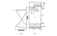
また、電気的特性を向上させた逆阻止IGBTとして、次の装置が公知である。図17は、従来の逆阻止IGBTの順方向電圧印加時および逆方向電圧印加時の電界強度分布を示す説明図である。図17(a)には、従来の逆阻止IGBTの要部の断面構造を示す。図17(b)には、図17(a)に示す逆阻止IGBTの厚さをy軸に示し、順方向電圧印加時および逆方向電圧印加時のそれぞれの電界強度分布をx軸に示す。y軸の距離とは、基板裏面(pコレクタ領域10とコレクタ電極11との界面)を0(ゼロ)としたエミッタ方向への距離である。図17(a)に示す逆阻止IGBTでは、n-ドリフト領域1とpベース領域2との界面およびn-ドリフト領域1とpコレクタ領域10との界面にそれぞれ同導電型で高不純物濃度の緩衝層201、202を形成することにより、順方向耐圧値および逆方向耐圧値の揃ったIGBTとすることができる(例えば、下記特許文献3参照。)。
Moreover, the following apparatus is well-known as reverse blocking IGBT which improved the electrical property. FIG. 17 is an explanatory diagram showing the electric field strength distribution when applying a forward voltage and applying a reverse voltage in a conventional reverse blocking IGBT. FIG. 17A shows a cross-sectional structure of a main part of a conventional reverse blocking IGBT. In FIG. 17 (b), the thickness of the reverse blocking IGBT shown in FIG. 17 (a) is shown on the y-axis, and the electric field intensity distributions at the time of forward voltage application and reverse voltage application are shown on the x-axis. The y-axis distance is a distance in the emitter direction where the back surface of the substrate (interface between the
また、電気的特性を向上させたIGBTとして、pベース領域とn-ドリフト領域との境界の少なくとも一部にn-ドリフト領域と同導電型で高不純物濃度領域を設けることにより、チャネル長を短縮し、オン状態の電圧降下を低減させた装置が提案されている(例えば、下記特許文献4参照。)。 Moreover, as an IGBT with improved electrical characteristics, the channel length is shortened by providing a high impurity concentration region of the same conductivity type as that of the n − drift region at least part of the boundary between the p base region and the n − drift region. And the apparatus which reduced the voltage drop of an ON state is proposed (for example, refer the following patent document 4).
また、電気的特性を向上させた別のIGBTとして、次の装置が提案されている。nドリフト領域のpコレクタ領域に近い部分に短寿命領域を形成する。短寿命領域は、n型でnベース層よりも高濃度にドープされている。この構成により、NPT(ノンパンチスルー)型IGBTの漏れ電流を低減することができる(例えば、下記特許文献5参照。)。
Moreover, the following apparatus is proposed as another IGBT which improved the electrical property. A short-life region is formed in a portion of the n drift region close to the p collector region. The short-life region is n-type and is doped at a higher concentration than the n base layer. With this configuration, the leakage current of the NPT (non-punch through) IGBT can be reduced (for example, see
また、電気的特性を向上させた別のIGBTとして、第2導電型コレクタ領域と離して第1導電型半導体基板の不純物濃度より高い不純物濃度で、第1導電型半導体基板内に形成された第1導電型フィールドストップ領域とを有する装置が提案されている(例えば、下記特許文献6参照。)。下記特許文献6では、コレクタ領域に部分的な欠損があった場合でも、オン状態における電圧降下特性の上昇や耐圧特性の低下が抑制される。
As another IGBT having improved electrical characteristics, a second IGBT formed in the first conductivity type semiconductor substrate at an impurity concentration higher than the impurity concentration of the first conductivity type semiconductor substrate apart from the second conductivity type collector region. A device having one conductivity type field stop region has been proposed (see, for example,
また、電気的特性を向上させた双方向IGBTとして、次の装置が提案されている。半導体基板の両主面に形成したトレンチ内に、それぞれゲート酸化膜を介してゲート電極が埋設され、半導体基板の両主面にトレンチ型のMOSゲート(金属−酸化膜−半導体からなる絶縁ゲート)構造(以下、トレンチゲートMOS構造とする)が構成されている。半導体基板の両主面のドリフト領域とベース層との界面に、ドリフト領域と同導電型で、かつドリフト領域よりも高濃度の緩衝層が設けられている。さらに、オフ電圧印加時にドリフト領域に拡がる空乏層が十分に伸びて高濃度の緩衝層に到達するパンチスルー型の構造とする。このような構造によって、双方向の耐圧を同程度に向上させ、ターンオフ時の振動波形をなくすことができるとともに、双方向にゲート制御することができる(例えば、下記特許文献7参照。)。
Further, the following devices have been proposed as bidirectional IGBTs with improved electrical characteristics. Gate electrodes are buried in the trenches formed on both main surfaces of the semiconductor substrate via gate oxide films, respectively, and trench-type MOS gates (insulated gates made of metal-oxide film-semiconductor) are formed on both main surfaces of the semiconductor substrate. A structure (hereinafter referred to as a trench gate MOS structure) is formed. A buffer layer having the same conductivity type as the drift region and having a higher concentration than the drift region is provided at the interface between the drift region and the base layer on both main surfaces of the semiconductor substrate. Furthermore, a depletion layer that extends into the drift region when an off voltage is applied is sufficiently extended to reach a high-concentration buffer layer. With such a structure, the bidirectional breakdown voltage can be improved to the same extent, the vibration waveform at turn-off can be eliminated, and gate control can be performed bidirectionally (see, for example,
また、電気的特性を向上させた逆阻止IGBTとして、コレクタ電極側に第2トレンチ溝を形成し、この第2トレンチ溝の表面に酸化膜を被覆し、ポリシリコンを充填し、第2トレンチ溝に挟まれた箇所に第2nバッファ領域を形成し、逆バイアス時の空乏層の伸びが第2nバッファ領域を飛び越してn-ドリフト領域へ拡がるようにすることで、順耐圧と同等の逆耐圧をPT型構造で得た装置が提案されている(例えば、下記特許文献8参照。)。
Also, as a reverse blocking IGBT with improved electrical characteristics, a second trench groove is formed on the collector electrode side, an oxide film is coated on the surface of the second trench groove, polysilicon is filled, and the second trench groove is formed. A second n buffer region is formed at a location sandwiched between and the depletion layer during reverse biasing extends over the second n buffer region and spreads to the n − drift region. An apparatus obtained with a PT-type structure has been proposed (see, for example,
しかしながら、前述の特許文献1に示す逆阻止IGBTでは、逆方向耐圧が、順方向耐圧に比べて低くなり易いという問題が生じる。以下、その理由について説明する。プレーナ形逆阻止IGBTは、逆阻止能力を確保するために、半導体基板のおもて面から裏面側のp+コレクタ領域に達するp+分離領域を必要とする。このp+分離領域を形成するために必要な高温で長時間のドライブ拡散(熱処理)は、n型のシリコン基板の面荒れを防ぐために酸素雰囲気中で行われる。この熱処理の拡散時間については、例えば、600V用耐圧デバイスでは1300℃の温度で100時間程度、1200V用の耐圧デバイスでは1300℃の温度で200時間程度を必要とする。
However, the reverse blocking IGBT shown in
このような高温長時間の熱処理が酸素雰囲気でシリコン基板に加えられることによりドーピングされた酸素原子がドナー化し、特にシリコン基板の不純物濃度が低い場合に酸素原子のドナー化による影響を受けてシリコン基板の酸素濃度が高くなる。シリコン基板の表面付近の酸素濃度は外方拡散により低下するため、シリコン基板の不純物濃度分布は、基板両主面から深さ方向に数μm〜数十μmの幅(深さ)で低く、基板中央部で高くなる。また、この逆阻止IGBTの製造工程には、おもて面側に所要のMOSゲート構造およびアルミ電極膜の形成工程と、低オン電圧にしつつ耐圧に必要なnドリフト領域の厚さにするための裏面研削工程と、p+コレクタ領域およびコレクタ電極の形成工程とが含まれる。裏面研削工程におけるシリコン基板の裏面研削量は、当初のシリコン基板の厚さの半分以上と極めて大きい。このため、上述したように酸素原子のドナー化の影響を受けたシリコン基板は、裏面研削工程後には、裏面研削されるコレクタ側で不純物濃度が高く、エミッタ側では、外方拡散の影響で基板おもて面から深さ方向に数μm〜数十μmの幅(深さ)で傾斜して低下する不純物濃度分布となる。 Such a high-temperature and long-time heat treatment is applied to the silicon substrate in an oxygen atmosphere, so that doped oxygen atoms become donors, and particularly when the impurity concentration of the silicon substrate is low, the silicon substrate is affected by the oxygen atom donors. The oxygen concentration of becomes higher. Since the oxygen concentration in the vicinity of the surface of the silicon substrate decreases due to outward diffusion, the impurity concentration distribution of the silicon substrate is low at a width (depth) of several μm to several tens of μm in the depth direction from both main surfaces of the substrate. It gets higher at the center. Further, in the manufacturing process of the reverse blocking IGBT, a required MOS gate structure and an aluminum electrode film are formed on the front surface side, and the thickness of the n drift region necessary for the withstand voltage is set while maintaining a low on-voltage. And a step of forming a p + collector region and a collector electrode. The amount of back surface grinding of the silicon substrate in the back surface grinding process is extremely large, more than half of the original thickness of the silicon substrate. For this reason, as described above, the silicon substrate affected by the donor formation of oxygen atoms has a high impurity concentration on the collector side subjected to the back grinding after the back grinding process, and on the emitter side due to the influence of outward diffusion. The impurity concentration distribution decreases with a slope (width) of several μm to several tens of μm in the depth direction from the front surface.
この結果、nドリフト領域のコレクタ側の不純物濃度がエミッタ側の不純物濃度よりも高くなるため、逆阻止IGBTのエミッタ側にあるpベース接合(pベース領域とnドリフト領域との間のpn接合)から伸びる空乏層よりも、コレクタ接合(p+コレクタ領域とnドリフト領域との間のpn接合)から伸びる空乏層の方が伸び難くなる。これにより、低い電圧印加で電界が高くなり易くなるため、逆方向耐圧が順方向耐圧よりも小さくなる。このような酸素ドナーによる耐圧への影響は、シリコン基板の抵抗率が大きい場合、例えば耐圧が600V以上の場合に問題になり易い。一方、元来pn接合周縁の曲率半径についてはコレクタ接合(逆耐圧接合)の方がpベース接合(順耐圧接合)よりも大きく高耐圧が得られ易いこともあって、耐圧600V未満のデバイスでは、前述の酸素ドナーによる逆方向耐圧への影響を考慮しても、逆方向耐圧が順方向耐圧より大きくなり易い。 As a result, since the impurity concentration on the collector side of the n drift region becomes higher than the impurity concentration on the emitter side, the p base junction on the emitter side of the reverse blocking IGBT (pn junction between the p base region and the n drift region). The depletion layer extending from the collector junction (the pn junction between the p + collector region and the n drift region) is more difficult to extend than the depletion layer extending from. As a result, the electric field is likely to increase when a low voltage is applied, so that the reverse breakdown voltage is smaller than the forward breakdown voltage. Such an influence on the breakdown voltage due to the oxygen donor tends to cause a problem when the resistivity of the silicon substrate is large, for example, when the breakdown voltage is 600 V or higher. On the other hand, with regard to the radius of curvature of the pn junction periphery, the collector junction (reverse breakdown voltage junction) is larger than the p base junction (forward breakdown voltage junction) and a higher breakdown voltage is likely to be obtained. Considering the influence of the oxygen donor on the reverse breakdown voltage, the reverse breakdown voltage tends to be larger than the forward breakdown voltage.
また、前述の特許文献3や特許文献4に示す技術では、次の問題が生じる。例えば、図17(b)の破線に示すように、逆方向電圧印加(逆方向バイアス)時、コレクタ接合21から伸びる空乏層がエミッタ側の緩衝層(以下、シェル領域とする)201に達すると伸び難くなるため、電界が急激に高くなり、コレクタ接合21近傍で、電界ピーク(臨界電界強度)212を示す。一方、図17(b)の実線に示すように、順方向電圧印加(順方向バイアス)時、pベース接合20から伸びる空乏層はpコレクタ領域10に達すると同様に電界が急激に高くなり、pベース接合20の界面近傍で、電界ピーク211を示す。このため、順方向耐圧および逆方向耐圧がともに低下し易くなる。すなわち、シェル領域201およびバッファ領域(コレクタ側の緩衝層)202を設けたことにより、これらの領域がない場合に得られる順方向耐圧および逆方向耐圧を実現することができない虞が生じる。このような耐圧低下問題は、n-ドリフト領域1の不純物濃度を低くして設計耐圧を高くすることで回避することができることが知られている。
In addition, the following problems occur in the techniques shown in
しかしながら、n-ドリフト領域1の不純物濃度を低くすることで、空乏層は伸び易くなるが、半導体装置の動作中に空乏層がバッファ領域202に達するパンチスルー現象が発生し易くなる。この結果、ターンオフ時の電圧波形および電流波形(以下、ターンオフ波形とする)が振動するという新たな問題が生じる。また、逆阻止IGBTは、オン状態から逆阻止状態に切り換わる逆回復時に、過渡的に大きな電流が流れる特性(逆回復特性)を有する。このため、逆回復時の電圧波形および電流波形(以下、逆回復波形とする)が振動し易くなるという問題も生じる。さらに、ターンオフ波形および逆回復波形が振動した場合、ノイズが発生することや、電圧波形の振動が非常に大きくなったときに半導体装置が破壊されたりする恐れが生じる。
However, by reducing the impurity concentration of the n − drift region 1, the depletion layer is easily extended, but a punch-through phenomenon in which the depletion layer reaches the
本発明は、前述した従来技術による問題点を解消するため、逆方向耐圧の向上、順方向耐圧の向上、ターンオフ時の電圧波形および電流波形の振動の抑制、逆回復時の電圧波形および電流波形の振動を抑制することができる半導体装置を提供することを目的とする。 The present invention eliminates the above-mentioned problems caused by the prior art, and improves reverse breakdown voltage, forward breakdown voltage, suppression of voltage and current waveform oscillation during turn-off, voltage waveform and current waveform during reverse recovery. An object of the present invention is to provide a semiconductor device capable of suppressing the vibration of the semiconductor device.
上述した課題を解決し、本発明の目的を達成するため、この本発明にかかる半導体装置は、次の特徴を有する。ドリフト領域となる第1導電型の半導体基板の一方の主面の表面層に、第2導電型のベース領域が選択的に設けられている。前記ベース領域の内部に第1導電型のエミッタ領域が選択的に設けられている。前記半導体基板の一方の主面から前記エミッタ領域および前記ベース領域を貫通して前記ドリフト領域に達するトレンチが設けられている。前記トレンチの内壁に沿って絶縁膜が設けられている。前記トレンチ内部に前記絶縁膜を介してゲート電極が埋め込まれている。前記エミッタ領域および前記ベース領域に接するエミッタ電極が設けられている。前記ドリフト領域の内部に、前記ベース領域のドリフト領域側に接する第1導電型のシェル領域が設けられている。前記半導体基板の他方の主面の表面層に、第2導電型のコレクタ領域が設けられている。そして、前記シェル領域は、前記ドリフト領域よりも高い不純物濃度を有する。前記シェル領域中の第1導電型の不純物の実効ドーズ量が5.0×1012cm-2以下である。前記ドリフト領域は、前記エミッタ電極を正極とする逆方向の定格電圧印加時に前記コレクタ領域から拡がる空乏層が前記シェル領域もしくは前記トレンチの底部のうち前記コレクタ領域に近い方に到達しない抵抗率を有する。 In order to solve the above-described problems and achieve the object of the present invention, the semiconductor device according to the present invention has the following characteristics. A base region of the second conductivity type is selectively provided on the surface layer of one main surface of the first conductivity type semiconductor substrate serving as the drift region. A first conductivity type emitter region is selectively provided in the base region. A trench reaching the drift region from one main surface of the semiconductor substrate through the emitter region and the base region is provided. An insulating film is provided along the inner wall of the trench. A gate electrode is embedded in the trench through the insulating film. An emitter electrode is provided in contact with the emitter region and the base region. A shell region of a first conductivity type that contacts the drift region side of the base region is provided inside the drift region. A collector region of the second conductivity type is provided in the surface layer on the other main surface of the semiconductor substrate. The shell region has a higher impurity concentration than the drift region. The effective dose amount of the first conductivity type impurity in the shell region is 5.0 × 10 12 cm −2 or less. The drift region has a resistivity such that a depletion layer extending from the collector region when a reverse rated voltage is applied with the emitter electrode as a positive electrode does not reach the closer to the collector region of the bottom of the shell region or the trench. .
また、本発明にかかる半導体装置は、上述した発明において、前記シェル領域中の第1導電型の不純物の実効ドーズ量が4.0×1012cm-2以下であることが好ましい。 In the semiconductor device according to the present invention, the effective dose of the first conductivity type impurity in the shell region is preferably 4.0 × 10 12 cm −2 or less in the above-described invention.
また、本発明にかかる半導体装置は、上述した発明において、前記ドリフト領域と前記コレクタ領域との間に、漏れ電流を低減させるための、前記ドリフト領域よりも高い不純物濃度を有する第1導電型領域が設けられていることが好ましい。 In the semiconductor device according to the present invention, the first conductivity type region having a higher impurity concentration than the drift region for reducing leakage current between the drift region and the collector region in the above-described invention. Is preferably provided.
また、本発明にかかる半導体装置は、上述した発明において、前記ドリフト領域の外周端部に、前記半導体基板の一方の主面から前記コレクタ領域に達する第2導電型の分離領域をさらに備えることがより好ましい。 The semiconductor device according to the present invention may further include, in the above-described invention, an isolation region of a second conductivity type that reaches the collector region from one main surface of the semiconductor substrate at an outer peripheral end of the drift region. More preferred.
また、本発明にかかる半導体装置は、上述した発明において、前記ドリフト領域は、前記エミッタ電極を正極とする逆方向の定格電圧印加時、前記コレクタ領域から前記ベース領域に向かって拡がる空乏層が前記ベース領域もしくは前記トレンチの底部のうち前記コレクタ領域に近い方に到達しない抵抗率を有することが好適である。 Further, in the semiconductor device according to the present invention, in the above-described invention, the drift region has a depletion layer that extends from the collector region toward the base region when a reverse rated voltage is applied with the emitter electrode as a positive electrode. It is preferable to have a resistivity that does not reach the base region or the bottom of the trench closer to the collector region.
また、上述した課題を解決し、本発明の目的を達成するため、この発明にかかる半導体装置は、次の特徴を有する。ドリフト領域となる第1導電型の半導体基板の一方の主面の表面層に、第2導電型の第1ベース領域が選択的に設けられている。前記第1ベース領域の内部に第1導電型の第1エミッタ領域が選択的に設けられている。前記半導体基板の一方の主面から前記第1エミッタ領域および前記第1ベース領域を貫通して前記ドリフト領域に到達する第1トレンチが設けられている。前記第1トレンチの内壁に沿って第1絶縁膜が設けられている。前記第1トレンチの内部に前記第1絶縁膜を介して第1ゲート電極が埋め込まれている。前記第1エミッタ領域および前記第1ベース領域に接するエミッタ電極が設けられている。前記ドリフト領域の内部に、前記第1ベース領域の前記ドリフト領域側に接する第1導電型の第1シェル領域が設けられている。前記半導体基板の他方の主面の表面層に第2導電型の第2ベース領域が選択的に設けられている。前記第2ベース領域の内部に第1導電型の第2エミッタ領域が選択的に設けられている。前記半導体基板の他方の主面から前記第2エミッタ領域および前記第2ベース領域を貫通して前記ドリフト領域に到達する第2トレンチが設けられている。前記第2トレンチの内壁に沿って第2絶縁膜が設けられている。前記第2トレンチの内部に前記第2絶縁膜を介して第2ゲート電極が埋め込まれている。前記第2エミッタ領域および前記第2ベース領域に接する裏面電極が設けられている。前記ドリフト領域の内部に、前記第2ベース領域の前記ドリフト領域側に接する第1導電型の第2シェル領域が設けられている。そして、前記第1シェル領域および前記第2シェル領域は、前記ドリフト領域よりも高い不純物濃度を有する。前記第1シェル領域および前記第2シェル領域中の第1導電型の不純物の実効ドーズ量は5.0×1012cm-2以下である。前記ドリフト領域は、前記エミッタ電極を正極とする逆方向の定格電圧印加時に前記第2ベース領域から拡がる空乏層が前記第1シェル領域または前記第1トレンチの底部のうち前記第2シェル領域に近い方に到達しない抵抗率を有する。 In order to solve the above-described problems and achieve the object of the present invention, a semiconductor device according to the present invention has the following characteristics. A first base region of the second conductivity type is selectively provided on the surface layer of one main surface of the first conductivity type semiconductor substrate serving as the drift region. A first conductivity type first emitter region is selectively provided in the first base region. A first trench is provided that reaches the drift region from one main surface of the semiconductor substrate through the first emitter region and the first base region. A first insulating film is provided along the inner wall of the first trench. A first gate electrode is embedded in the first trench through the first insulating film. An emitter electrode in contact with the first emitter region and the first base region is provided. A first conductivity type first shell region in contact with the drift region side of the first base region is provided inside the drift region. A second base region of the second conductivity type is selectively provided on the surface layer of the other main surface of the semiconductor substrate. A second emitter region of the first conductivity type is selectively provided in the second base region. A second trench is provided that reaches the drift region from the other main surface of the semiconductor substrate through the second emitter region and the second base region. A second insulating film is provided along the inner wall of the second trench. A second gate electrode is embedded in the second trench through the second insulating film. A back electrode in contact with the second emitter region and the second base region is provided. Inside the drift region, a second shell region of a first conductivity type is provided in contact with the drift region side of the second base region. The first shell region and the second shell region have a higher impurity concentration than the drift region. The effective dose amount of the first conductivity type impurity in the first shell region and the second shell region is 5.0 × 10 12 cm −2 or less. In the drift region, a depletion layer that extends from the second base region when a reverse rated voltage is applied with the emitter electrode as a positive electrode is close to the second shell region in the bottom of the first shell region or the first trench. It has a resistivity that does not reach the direction.
また、本発明にかかる半導体装置は、上述した発明において、前記第2シェル領域中の第1導電型の不純物の実効ドーズ量が4.0×1012cm-2以下であることが望ましい。 In the semiconductor device according to the present invention, the effective dose of the first conductivity type impurity in the second shell region is preferably 4.0 × 10 12 cm −2 or less in the above-described invention.
また、本発明にかかる半導体装置は、上述した発明において、前記ドリフト領域は、前記エミッタ電極を正極とする逆方向の定格電圧印加時、前記第2ベース領域から前記第1ベース領域に向かって拡がる空乏層が前記第1ベース領域または前記第1トレンチの底部のうち前記第2シェル領域に近い方に到達しない抵抗率を有することが好ましい。 In the semiconductor device according to the present invention, in the above-described invention, the drift region extends from the second base region toward the first base region when a reverse rated voltage is applied with the emitter electrode serving as a positive electrode. It is preferable that the depletion layer has a resistivity that does not reach a side closer to the second shell region of the first base region or the bottom of the first trench.
上述した発明によれば、ドリフト領域の内部にベース領域に接するようにシェル領域を設けることによって、従来よりも半導体基板内の電界を緩和することができるため、順方向耐圧および逆方向耐圧を向上させることができる。また、上述した発明によれば、シェル領域中の第1導電型の不純物の実効ドーズ量を5.0×1012cm-2以下とすることで、逆回復波形の逆回復電流がマイナス値からゼロに収束するまでの期間を従来よりも早くすることができる。すなわち、従来よりも阻止電圧の回復を早めることができる。 According to the above-described invention, by providing the shell region so as to be in contact with the base region inside the drift region, the electric field in the semiconductor substrate can be relaxed more than before, so that the forward breakdown voltage and the reverse breakdown voltage are improved. Can be made. According to the above-described invention, the reverse recovery current of the reverse recovery waveform can be reduced from a negative value by setting the effective dose of the first conductivity type impurity in the shell region to 5.0 × 10 12 cm −2 or less. The period until convergence to zero can be made faster than before. That is, the recovery of the blocking voltage can be accelerated compared to the conventional case.
また、上述した課題を解決し、本発明の目的を達成するため、この発明にかかる半導体装置は、次の特徴を有する。第1半導体領域となる第1導電型の半導体基板の一方の主面の表面層に、第2導電型の第2半導体領域が選択的に設けられている。前記第2半導体領域の内部に、前記第1半導体領域よりも不純物濃度が高い第1導電型の第3半導体領域が選択的に設けられている。前記第2半導体領域の、前記第3半導体領域と前記第1半導体領域とに挟まれた部分の表面上に絶縁膜を介して第1電極が設けられている。前記第3半導体領域および前記第2半導体領域に接する第2電極が設けられている。前記半導体基板の他方の主面の表面層に、第2導電型の第4半導体領域が設けられている。前記第4半導体領域に接する第3電極が設けられている。前記第1半導体領域の内部の前記第4半導体領域側に、前記第4半導体領域の前記第1半導体領域側の少なくとも一部と対向する第1導電型の第5半導体領域が設けられている。前記第5半導体領域は、前記第1半導体領域よりも不純物濃度が高い。前記半導体基板の外周部に第2導電型の第6半導体領域が設けられている。前記第6半導体領域は、前記半導体基板の一方の主面から前記第1半導体領域を貫通して前記第4半導体領域に達する。そして、前記第5半導体領域中の第1導電型の不純物の総ドーズ量は2.0×1012cm-2以下である。 In order to solve the above-described problems and achieve the object of the present invention, a semiconductor device according to the present invention has the following characteristics. A second conductive type second semiconductor region is selectively provided on the surface layer of one main surface of the first conductive type semiconductor substrate to be the first semiconductor region. A first conductivity type third semiconductor region having an impurity concentration higher than that of the first semiconductor region is selectively provided inside the second semiconductor region. A first electrode is provided on the surface of the portion of the second semiconductor region sandwiched between the third semiconductor region and the first semiconductor region via an insulating film. A second electrode in contact with the third semiconductor region and the second semiconductor region is provided. A fourth semiconductor region of the second conductivity type is provided in the surface layer on the other main surface of the semiconductor substrate. A third electrode in contact with the fourth semiconductor region is provided. A fifth semiconductor region of a first conductivity type facing at least a part of the fourth semiconductor region on the first semiconductor region side is provided on the fourth semiconductor region side inside the first semiconductor region. The fifth semiconductor region has a higher impurity concentration than the first semiconductor region. A sixth semiconductor region of the second conductivity type is provided on the outer periphery of the semiconductor substrate. The sixth semiconductor region penetrates the first semiconductor region from one main surface of the semiconductor substrate and reaches the fourth semiconductor region. The total dose of the first conductivity type impurities in the fifth semiconductor region is 2.0 × 10 12 cm −2 or less.
また、上述した課題を解決し、本発明の目的を達成するため、この発明にかかる半導体装置は、次の特徴を有する。第1半導体領域となる第1導電型の半導体基板の一方の主面の表面層に、第2導電型の第2半導体領域が選択的に設けられている。前記第2半導体領域の内部に、前記第1半導体領域よりも不純物濃度が高い第1導電型の第3半導体領域が選択的に設けられている。前記半導体基板の一方の主面から前記第3半導体領域および前記第2半導体領域を貫通して前記第1半導体領域に達するトレンチが設けられている。前記トレンチの内壁に沿って絶縁膜が設けられている。前記トレンチ内部に前記絶縁膜を介して第1電極が埋め込まれている。前記第3半導体領域および前記第2半導体領域に接する第2電極が設けられている。前記半導体基板の他方の主面の表面層に、第2導電型の第4半導体領域が設けられている。前記第4半導体領域に接する第3電極が設けられている。前記第1半導体領域の内部の前記第4半導体領域側に、前記第4半導体領域の前記第1半導体領域側の少なくとも一部と対向する第1導電型の第5半導体領域が設けられている。前記第5半導体領域は、前記第1半導体領域よりも不純物濃度が高い。前記半導体基板の外周部に第2導電型の第6半導体領域が設けられている。前記第6半導体領域は、前記半導体基板の一方の主面から前記第1半導体領域を貫通して前記第4半導体領域に達する。そして、前記第5半導体領域中の第1導電型の不純物の総ドーズ量は2.0×1012cm-2以下である。 In order to solve the above-described problems and achieve the object of the present invention, a semiconductor device according to the present invention has the following characteristics. A second conductive type second semiconductor region is selectively provided on the surface layer of one main surface of the first conductive type semiconductor substrate to be the first semiconductor region. A first conductivity type third semiconductor region having an impurity concentration higher than that of the first semiconductor region is selectively provided inside the second semiconductor region. A trench reaching the first semiconductor region from one main surface of the semiconductor substrate through the third semiconductor region and the second semiconductor region is provided. An insulating film is provided along the inner wall of the trench. A first electrode is embedded in the trench through the insulating film. A second electrode in contact with the third semiconductor region and the second semiconductor region is provided. A fourth semiconductor region of the second conductivity type is provided in the surface layer on the other main surface of the semiconductor substrate. A third electrode in contact with the fourth semiconductor region is provided. A fifth semiconductor region of a first conductivity type facing at least a part of the fourth semiconductor region on the first semiconductor region side is provided on the fourth semiconductor region side inside the first semiconductor region. The fifth semiconductor region has a higher impurity concentration than the first semiconductor region. A sixth semiconductor region of the second conductivity type is provided on the outer periphery of the semiconductor substrate. The sixth semiconductor region penetrates the first semiconductor region from one main surface of the semiconductor substrate and reaches the fourth semiconductor region. The total dose of the first conductivity type impurities in the fifth semiconductor region is 2.0 × 10 12 cm −2 or less.
また、本発明にかかる半導体装置は、上述した発明において、前記第5半導体領域は、前記第4半導体領域の前記第1半導体領域側全面と対向することが好ましい。 In the semiconductor device according to the present invention, in the above-described invention, it is preferable that the fifth semiconductor region opposes the entire surface of the fourth semiconductor region on the first semiconductor region side.
また、本発明にかかる半導体装置は、上述した発明において、前記第2半導体領域、前記第3半導体領域、前記第4半導体領域、前記第1電極、前記第2電極および前記第3電極を有する活性領域が設けられている。前記半導体基板の一方の主面の表面層に前記活性領域を囲むように耐圧構造領域が設けられている。前記耐圧構造領域は、複数の第2導電型の第7半導体領域を有していてもよい。 The semiconductor device according to the present invention is the active device having the second semiconductor region, the third semiconductor region, the fourth semiconductor region, the first electrode, the second electrode, and the third electrode in the above-described invention. An area is provided. A breakdown voltage structure region is provided in a surface layer on one main surface of the semiconductor substrate so as to surround the active region. The breakdown voltage structure region may include a plurality of second conductivity type seventh semiconductor regions.
また、本発明にかかる半導体装置は、上述した発明において、前記第1半導体領域は、前記第2電極を正極とする逆方向の定格電圧印加時に前記第2半導体領域から前記第5半導体領域に向かって拡がる空乏層が前記第5半導体領域に到達しない抵抗率を有することが好ましい。 In the semiconductor device according to the present invention, in the above-described invention, the first semiconductor region moves from the second semiconductor region to the fifth semiconductor region when a reverse rated voltage is applied with the second electrode as a positive electrode. It is preferable that the depletion layer that spreads out has a resistivity that does not reach the fifth semiconductor region.
上述した発明によれば、第5半導体領域を設けることにより、逆方向電圧印加時に半導体基板内の電界強度を均一にすることができるため、逆方向耐圧を向上させることができる。また、上述した発明によれば、第1半導体領域内部の第4半導体領域側に第5半導体領域を設けることにより、順方向電圧印加時に、第5半導体領域と第4半導体領域との間に中性領域が残るため、ターンオフ時の電圧波形および電流波形の振動を抑制することができる。 According to the above-described invention, by providing the fifth semiconductor region, the electric field strength in the semiconductor substrate can be made uniform when the reverse voltage is applied, so that the reverse breakdown voltage can be improved. Further, according to the above-described invention, by providing the fifth semiconductor region on the fourth semiconductor region side inside the first semiconductor region, the intermediate voltage is applied between the fifth semiconductor region and the fourth semiconductor region when the forward voltage is applied. Therefore, the vibration of the voltage waveform and the current waveform at the time of turn-off can be suppressed.
本発明にかかる半導体装置によれば、逆方向耐圧の向上、順方向耐圧の向上、ターンオフ時の電圧波形および電流波形の振動の抑制、逆回復時の電圧波形および電流波形の振動を抑制することができる半導体装置を提供することができるという効果を奏する。 According to the semiconductor device of the present invention, the reverse breakdown voltage is improved, the forward breakdown voltage is improved, the vibration of the voltage waveform and the current waveform at turn-off is suppressed, and the vibration of the voltage waveform and the current waveform at the time of reverse recovery is suppressed. There is an effect that it is possible to provide a semiconductor device that can be used.
以下、本発明にかかる半導体装置の好適な実施の形態について、添付図面を参照して詳細に説明する。以下の説明では、逆阻止型半導体装置として逆阻止IGBTの場合を例に説明し、また、第1導電型をn型、第2導電型をp型として説明する。本明細書および添付図面においては、nまたはpを冠記した層や領域では、それぞれ電子または正孔が多数キャリアであることを意味する。また、nやpに付す+および−は、それぞれそれが付されていない層や領域よりも相対的に不純物濃度が高いまたは低いことを意味する。なお、以下の実施の形態の説明および添付図面において、同様の構成には同一の符号を付し、重複する説明を省略する。また、以下の実施の形態で説明される添付図面は、見易くまたは理解し易くするために正確なスケール、寸法比で描かれていない。本発明はその要旨を超えない限り、以下に説明する実施の形態の記載に限定されるものではない。 DESCRIPTION OF EMBODIMENTS Hereinafter, preferred embodiments of a semiconductor device according to the present invention will be described in detail with reference to the accompanying drawings. In the following description, the case of a reverse blocking IGBT will be described as an example of the reverse blocking semiconductor device, and the first conductivity type will be described as n-type and the second conductivity type will be described as p-type. In the present specification and the accompanying drawings, it means that electrons or holes are majority carriers in layers and regions with n or p, respectively. Further, + and − attached to n and p mean that the impurity concentration is relatively higher or lower than that of the layer or region not attached thereto. Note that, in the following description of the embodiments and the accompanying drawings, the same reference numerals are given to the same components, and duplicate descriptions are omitted. In addition, the accompanying drawings described in the following embodiments are not drawn to an accurate scale and dimensional ratio for easy understanding or understanding. The present invention is not limited to the description of the embodiments described below unless it exceeds the gist.
(実施の形態1)
実施の形態1にかかる半導体装置について、逆阻止IGBTを例に説明する。図1は、本発明の実施の形態1にかかる逆阻止IGBTの構成を示す断面図である。図1に示すように、この逆阻止IGBTは、n-ドリフト領域1aとなるFZシリコン基板(半導体基板)上に、活性領域200と、活性領域200の外側に設けられる耐圧構造領域100と、耐圧構造領域100の外側に設けられる分離部130とを備えている。半導体基板の厚さは、例えば600V耐圧クラスの逆阻止IGBTの特性に悪影響を及ぼさないためには、例えば90μm以上であればよく、n-ドリフト領域1aは80μm以上であればよい。活性領域200には、n-ドリフト領域1aの基板おもて面側に設けられたトレンチゲートMOS構造およびn-ドリフト領域1aの基板裏面側に設けられたpコレクタ領域10aおよびコレクタ電極11aを有する縦型の逆阻止IGBTが構成されている。トレンチゲートMOS構造の詳細な説明については後述する。
(Embodiment 1)
The semiconductor device according to the first embodiment will be described by taking a reverse blocking IGBT as an example. FIG. 1 is a cross-sectional view illustrating a configuration of a reverse blocking IGBT according to a first embodiment of the present invention. As shown in FIG. 1, the reverse blocking IGBT includes an
耐圧構造領域100の基板おもて面側に設けられた耐圧構造は、活性領域200と分離部130との間で、活性領域200を囲む所定のパターンを有する。耐圧構造領域100は、IGBTを構成するpn主接合終端面の電界強度を緩和し所望の耐圧と耐圧信頼性とを実現する機能を有する。pn主接合とは、pベース領域2aとn-ドリフト領域1aとの間のpn接合(pベース接合)である。耐圧構造領域100の耐圧構造については後述する。分離部130は、ウエハを個々のチップにダイシングする際に半導体基板の側面となる切断面を有し、この切断面に沿って形成される。このため、分離部130は、この切断面に生じる結晶欠陥が少なくとも耐圧構造領域100に悪影響を及ぼすことのない幅を必要とする。分離部130は、n-ドリフト領域1aの外周側端部にあって、n-ドリフト領域1aの基板おもて面から基板裏面側のpコレクタ領域10aに達する深さの分離領域31aを有する。逆方向電圧の印加時、空乏層は、半導体基板の裏面側のコレクタ接合(pコレクタ領域10aとn-ドリフト領域1aとの間のpn接合)21と、分離領域31aとn-ドリフト領域1aとの間のpn接合(以下、分離領域接合とする)21aとから、pベース領域2aに向かって伸びる。これにより、逆方向電圧の印加時に、半導体基板の側面に空乏層が達することを防止して漏れ電流の発生を防止し、逆方向耐圧を得ることができる。
The breakdown voltage structure provided on the substrate front surface side of the breakdown
次に、活性領域200の構成について詳細に説明する。図2は、図1の逆阻止IGBTの活性領域200の構成を示す断面図である。活性領域200には、n-ドリフト領域1aとなる半導体基板のおもて面に、複数の第1トレンチ5が所定の間隔で設けられている。半導体基板のおもて面の表面層には、pベース領域2aが第1トレンチ5に挟まれるように設けられている。pベース領域2aは、n-ドリフト領域1aよりも高い不純物濃度を有する。隣り合う第1トレンチ5に挟まれた部分においてpベース領域2aの基板おもて面側の表面層には、n+エミッタ領域3aおよびp+ボディ領域4aが選択的に設けられる。p+ボディ領域4aは、pベース領域2aよりも高い不純物濃度を有する。pベース領域2aの、隣り合う第1トレンチ5に挟まれた部分には、n+エミッタ領域3aおよびp+ボディ領域4aが設けられた構成の部分と、この構成からn+エミッタ領域3aがない構成の部分とが交互に並んで設けられている。
Next, the configuration of the
nシェル領域13は、n-ドリフト領域1aとpベース領域2aとの間であって第1トレンチ5に挟まれる部分に設けられている。また、nシェル領域13は、少なくともpベース領域2aの下(n-ドリフト領域1a側)の領域をすべて占めるように設けられるのがよい。その理由は、pコレクタ領域10aからpベース領域2aへの少数キャリアの注入を抑制することができ、かつ輸送効率を低減するからである。望ましくは、nシェル領域13は、活性領域200内のpベース領域2aの下の領域全体を囲むように設けられているのがよい。すなわち、pベース領域2aとn-ドリフト領域1aとが接する領域を完全になくすことで、確実に、pコレクタ領域10aからpベース領域2aへの少数キャリアの注入を抑制し、かつ輸送効率を低減することができる。また、nシェル領域13は、図2では、第1トレンチ5に完全に挟まれているが、一部が第1トレンチ5に挟まれて、一部は第1トレンチ5の下層に及ぶ深さ(第1トレンチ5の底部を覆う深さ)を有するnシェル領域13を設けてもよい。エミッタ電極9aは、n+エミッタ領域3aおよびp+ボディ領域4aの表面に共通に接する。また、エミッタ電極9aは、層間絶縁膜8aによってゲート電極7aとは電気的に絶縁されている。
The
前述の第1トレンチ5の構造について、さらに説明する。第1トレンチ5は、n+エミッタ領域3aおよびpベース領域2aを貫通する深さを必ず必要とするが、前述のnシェル領域13に対しては、このnシェル領域13の中間の深さでも、貫通する深さであってもよい。第1トレンチ5内に形成されるMOSゲート構造(トレンチゲートMOS構造)は、従来と同様に、第1トレンチ5の内壁に沿ってゲート絶縁膜6aが設けられ、第1トレンチ5の内部にゲート絶縁膜6aを介してポリシリコンからなるゲート電極7aが埋設される構造であってもよい。
The structure of the
また、nシェル領域13は、n-ドリフト領域1aよりも高い不純物濃度を有する。そして、n-ドリフト領域1aは、pコレクタ領域10aからnシェル領域13に向かって拡がる空乏層がnシェル領域13に到達しないという条件を満たすような抵抗率を有することが好ましい。少なくとも、n-ドリフト領域1aは、定格電圧と等しい逆方向電圧が印加された時に、pコレクタ領域10aからnシェル領域13に向かって拡がる空乏層がnシェル領域13に到達しない抵抗率を有する必要がある。定格電圧600Vの逆阻止IGBTの耐圧を、できるだけ低いオン電圧で達成するには、n-ドリフト領域1aの抵抗率は、例えば22Ωcm以上35Ωcm以下であり、n-ドリフト領域1aの幅(厚さ)は例えば80μm以上100μm以下であるのがよい。これにより、逆方向電圧の回復時、空乏層がnシェル領域13に達しないようにすることができる。
Further,
一方、半導体基板の裏面側において、n-ドリフト領域1aとpコレクタ領域10aとの間にはpコレクタ領域10aに接するnLCS(Leakage Current Stop)領域12が設けられている。nLCS領域12を設ける理由は、pコレクタ領域10aからnLCS領域12への少数キャリアの注入を抑制することができ、かつ輸送効率を低減するためである。nLCS領域12は、漏れ電流を低減させる機能を有する。
On the other hand, on the back surface side of the semiconductor substrate, an nLCS (Leakage Current Stop)
また、nLCS領域12は、n-ドリフト領域1aよりも高い不純物濃度を有する。さらに、n-ドリフト領域1aは、順方向電圧、好ましくは定格電圧と等しい順方向電圧が印加された時に、pベース領域2aからnLCS領域12に向かって拡がる空乏層がnLCS領域12に到達しない抵抗率を有する。さらに、nLCS領域12は、nLCS領域12中のn型不純物の実効ドーズ量(以下、nLCS領域12の実効ドーズ量とする)が5.0×1012cm-2以下となる不純物濃度を有する。この不純物濃度については、nLCS領域12中の実効ドーズ量がnLCS領域12中のある領域に片寄って分布されていたとしても、nLCS領域12全体に含まれるn型不純物の実効ドーズ量が平均して5.0×1012cm-2以下となるようにnLCS領域12中に含まれていればよく、nLCS領域12が特定の決まった不純物濃度分布である必要はない。望ましくは、nLCS領域12は、nLCS領域12の実効ドーズ量が4.0×1012cm-2以下となる不純物濃度を有するのがよい。その理由は、逆阻止IGBTに特有の動作である逆回復損失(逆方向電圧の回復時のスイッチング損失)とターンオン損失の総和を抑えることができるからである。
The
次に、耐圧構造領域100の構成について説明する。図3は、図1の逆阻止IGBTの耐圧構造領域100の構成を示す断面図である。耐圧構造領域100は、活性領域200の外周にリング状平面パターンで形成される。具体的には、耐圧構造領域100には、耐圧保護膜としてn-ドリフト領域1aの基板おもて面側の表面を覆うフィールド絶縁膜8bが設けられている。このフィールド絶縁膜8bの下層となるn-ドリフト領域1aの基板おもて面側の表面層には、電気的にフローティングのp型領域であるフィールドリミッティングリング(以降、FLR:Field Limiting Ring)101が活性領域200の表層を囲むように複数、リング状平面パターンで設けられている。フィールド絶縁膜8bにはFLR101の表面をリング状の平面パターンで露出させる開口部8cがそれぞれ設けられる。複数のFLR101上には、フィールド絶縁膜8bの開口部8cを介して、フローティングの導電膜であるフィールドプレート(以降、FP)14がFLR101の表面形状に沿ってそれぞれ設けられている。
Next, the configuration of the breakdown
次に、実施の形態1にかかる逆阻止IGBTの電界強度分布について説明する。図4は、本発明の実施の形態1にかかる逆阻止IGBTの活性領域における電界強度分布を示す特性図である。図14は、実施の形態1にかかる逆阻止IGBTの別の一例を示す断面図である。図4には、図1、2の実施の形態1にかかる逆阻止IGBTの電界強度分布(図4(a))と、図14および前記特許文献6にそれぞれ記載の双方向IGBTの電界強度分布(図4(b)、4(c))とを示す。図4(a)、4(b)は、pコレクタ領域10a表面(pコレクタ領域10aとコレクタ電極11aとの界面)からの距離yと電界強度Eとの関係を示す電界強度分布特性図である(4(c)においても同様)。
Next, the electric field strength distribution of the reverse blocking IGBT according to the first embodiment will be described. FIG. 4 is a characteristic diagram showing the electric field strength distribution in the active region of the reverse blocking IGBT according to the first embodiment of the present invention. FIG. 14 is a cross-sectional view of another example of the reverse blocking IGBT according to the first embodiment. 4 shows the electric field strength distribution (FIG. 4A) of the reverse blocking IGBT according to the first embodiment of FIGS. 1 and 2, and the electric field strength distribution of the bidirectional IGBT described in FIG. 14 and
図4(a)に示すように、図1、2の実施の形態1にかかる逆阻止IGBTでは、第1トレンチ5がnシェル領域13を貫通しているため、順バイアス時(順方向電圧印加時:図4(a)の実線)に生じる電界ピーク(臨界電界強度)は、図17(b)に示す従来の逆阻止IGBTの電界ピーク211のようにpベース接合20の近傍ではなく、nシェル領域13とn-ドリフト領域1aとの境界近傍の第1トレンチ5底部の位置(シェル領域に平行な破線)のn-ドリフト領域1a内にある。さらに、実施の形態1にかかる逆阻止IGBTにおいては、電界ピーク前後の電界強度の傾斜が、図17(b)に示す従来構造の電界ピーク211前後の傾斜に比べて緩やかになっていることが特長である。
As shown in FIG. 4A, in the reverse blocking IGBT according to the first embodiment shown in FIGS. 1 and 2, since the
また、実施の形態1にかかる逆阻止IGBTでは、逆バイアス時(逆方向電圧印加時:図4(a)の傾斜破線)にpコレクタ領域10aとnLCS領域12との境界近傍に生じる電界ピークが順バイアスと同様(順バイアスとは電界ピークが生じる方向が逆であるが)に図17(b)に示す従来構造の電界ピーク212前後の傾斜よりも緩やかになっている。また、逆バイアス時の電界強度分布のエミッタ側は、nシェル領域13まで達しておらずn-ドリフト領域1a内にある。これは、コレクタ接合21からエミッタ方向に向かって伸びる空乏層がnシェル領域13に到達する前にアバランシェ降伏電界に達するようにすることを示している。
Further, in the reverse blocking IGBT according to the first embodiment, an electric field peak generated in the vicinity of the boundary between the
また、図14に示す基板の両主面側にそれぞれトレンチゲートMOS構造を有する双方向IGBTでは、第1、2シェル領域(nシェル領域)13、13aはそれぞれ基板の両主面側で第1、2トレンチ5、5a間に挟まれた狭い領域に設けられている。このため、図4(b)に示すように、順方向電圧印加時および逆方向電圧印加時の両方で電界ピークの位置が第1、2シェル領域13、13aとn-ドリフト領域1aとの境界近傍の第1、2トレンチ5、5a底部の位置(シェル領域に平行な破線)に移動するとともに、電界強度の傾斜が図17に示す従来構造よりも緩やかになる。さらに、pベース接合20からpコレクタ領域10a(図14のpベース領域2bに相当)に向かって伸びる空乏層(傾斜実線)は、第2シェル領域13aに到達する前にアバランシェ降伏を生じさせる臨界電界強度に達することが確認された。また、コレクタ接合21から第1シェル領域13に向かって伸びる空乏層(傾斜破線)は、第1シェル領域13に到達する前にアバランシェ降伏を生じさせる臨界電界強度に達することが確認された。図14では、基板おもて面側のnシェル領域13を第1シェル領域とし、基板裏面側のnシェル領域を第2シェル領域13aとしている。また、基板裏面側のトレンチゲートMOS構造を構成するトレンチ5aを第2トレンチとしている。図14に示す実施の形態1にかかる逆阻止IGBTの別の一例の構成については後述する。
Further, in the bidirectional IGBT having a trench gate MOS structure on both main surface sides of the substrate shown in FIG. 14, the first and second shell regions (n-shell regions) 13 and 13a are first on both main surface sides of the substrate. It is provided in a narrow region sandwiched between the two
前述のように、nシェル領域13をpベース領域2aとn-ドリフト領域1aとの間の第1トレンチ5間に設けることにより電界ピーク前後の傾斜が緩やかになる理由は、次のとおりである。pベース接合20の逆バイアス時には、狭い第1トレンチ5間のnシェル領域13は、pベース領域2aとのpn接合から空乏化するだけでなく、nシェル領域13を挟み込む両側の第1トレンチ5内のゲート絶縁膜6aとの境界からも空乏化する。このため、nシェル領域13の不純物濃度が高くても、nシェル領域13は低い順バイアスで完全に空乏化し易くなる。これにより、等電位間隔が広がり、電界強度の上昇が少なくなることで電界ピーク前後の傾斜が緩くなる。前述の狭い第1トレンチ5間とは、例えば、4μm〜5μmのトレンチ間隔である。
As described above, the reason why the inclination before and after the electric field peak becomes gentle by providing the
本発明にかかる逆阻止IGBTは、前述の電界強度分布となるように、前述の条件でnシェル領域13が設けられる。本発明にかかる双方向IGBTは、前述の電界強度分布となるように、前述の条件で第1シェル領域13または第2シェル領域13aが設けられる。かつ、本発明にかかる逆阻止IGBTおよび双方向IGBTは、前述のように定格電圧印加でn-ドリフト領域1a内を空乏層が完全に伸び切らない条件でn-ドリフト領域1aが設けられている。
The reverse blocking IGBT according to the present invention is provided with the
次に、前述の図1、2の実施の形態1にかかる逆阻止IGBT(以下、第1実施例とする)の電流特性について検証した。第1実施例において、定格電圧は600Vとした。半導体基板の抵抗率および厚さを、それぞれ28Ωcmおよび80μmとした。すなわち、n-ドリフト領域1aの抵抗率は28Ωcmである。第1トレンチ5の幅を1.5μm、深さを5.0μm、第1トレンチ5の配置間隔4.5μmとした。以下、図5〜図10を参照して、この第1実施例の電流特性について説明する。図5は、図2の切断線A−A’における実効ドーズ量の分布を示す特性図である。縦軸は不純物濃度(cm-3)を、横軸はエミッタ表面からの距離(μm)である(図6、22においても同様)。エミッタ表面とは、n+エミッタ領域3aとエミッタ電極9aとの境界、すなわち半導体基板のおもて面である。図6は、図2の切断線B−B’における実効ドーズ量の分布を示す特性図である。図5の縦軸に示す不純物濃度は、半導体基板おもて面からある深さ(切断線A−A’)における領域の単位体積あたりの実効ドーズ量を不純物濃度として示したものである。また、図6の縦軸に示す不純物濃度も同様に、n-ドリフト領域1aからp+ボディ領域4aへの方向での、ある距離における領域の単位体積あたりの実効ドーズ量を不純物濃度として示す。nシェル領域13に相当する領域の深さごとの実効ドーズ量を積分し、nシェル領域13の実効的な不純物濃度を算出した。すなわち、図5に示すnシェル領域13の実効ドーズ量の分布の分布形状内の領域が、nシェル領域13の実効ドーズ量である。
Next, the current characteristics of the reverse blocking IGBT (hereinafter referred to as the first example) according to the first embodiment shown in FIGS. In the first embodiment, the rated voltage was 600V. The resistivity and thickness of the semiconductor substrate were 28 Ωcm and 80 μm, respectively. That is, the resistivity of the n − drift region 1a is 28 Ωcm. The width of the
n-ドリフト領域1aの単位面積あたりの実効ドーズ量とは、n-ドリフト領域1aのnシェル領域13が設けられる領域中の、n-ドリフト領域1aの単位面積あたりの実効ドーズ量である。n-ドリフト領域1aの単位面積あたりの実効ドーズ量は、nシェル領域13と同様の方法で算出している。図7は、実施の形態1にかかる逆阻止IGBTのnシェル領域13の実効ドーズ量と逆方向漏れ電流との関係について示す特性図である。nシェル領域13の実効ドーズ量(N−Shell Dose)が異なる複数の第1実施例を作製(製造)した。nシェル領域13の実効ドーズ量を、それぞれ1×1011cm-2〜6.8×1012cm-2とした。そして、これらの第1実施例についてそれぞれ逆方向漏れ電流を測定した。また、比較として、nシェル領域が設けられていない逆阻止IGBTを準備し(以下、比較例とする)、逆方向漏れ電流を測定した。
n - The effective dose per unit area of the
図7では、実効ドーズ量がゼロの場合を比較例として逆方向漏れ電流を示し、nシェル領域13の実効ドーズ量が異なる複数の第1実施例の逆方向漏れ電流(縦軸)を示すために、横軸をnシェル領域13の実効ドーズ量としている。n-ドリフト領域1aの厚さは80μmである。図7に示す結果より、比較例の漏れ電流は6.0×10⁻⁵A(0.06mA)at600Vを示すことが確認された。一方、表面不純物濃度1.8×1012cm-3以上のnシェル領域13を設けた第1実施例では、n-ドリフト領域1aの厚さを薄く(80μm)しても、逆方向漏れ電流を実質的にゼロ程度に低減させることができることが確認された。また、第1実施例は、nシェル領域13の実効ドーズ量が多いほど、逆方向漏れ電流を低減することができることがわかった。その理由は、nシェル領域13がn-ドリフト領域1aとpベース領域2aとの間に設けられているため、pコレクタ領域10a、n-ドリフト領域1aおよびpベース領域2a(p+ボディ領域4a)からなるpnpトランジスタの電流増幅率が小さくなるからである。なお、n-ドリフト領域1aの厚さが100μmで実効ドーズ量がゼロの場合の比較例では、漏れ電流が1.1×10-5A(0.011mA)at600Vを示すことが確認されている。
In FIG. 7, the reverse leakage current is shown as a comparative example when the effective dose is zero, and the reverse leakage current (vertical axis) of a plurality of first embodiments having different effective doses in the n-
次に、nシェル領域13の実効ドーズ量(N−Shell Dose)と、ターンオフ損失(Err:逆回復損失)およびターンオン(Eon)損失の和との関係について説明する。図8は、実施の形態1にかかる逆阻止IGBTのnシェル領域13の実効ドーズ量とターンオフ損失およびターンオン損失の和との関係について示す特性図である。逆阻止IGBTは、逆並列接続でマトリクスコンバータの双方向スイッチングデバイスとして使用する場合、従来のIGBTを用いた双方向スイッチングデバイスの場合のIGBTにシリーズ接続される逆耐圧用のダイオード(フリーホイールダイオード)として機能するステージがあるため、逆回復損失やターンオン損失が小さいことが望ましい。図8には、前述の第1実施例と比較例の逆回復損失およびターンオン損失をそれぞれ測定した結果を示す。
Next, the relationship between the effective dose amount (N-Shell Dose) of the
図8では、比較例であるnシェル領域のない逆阻止IGBTの逆回復損失とターンオン損失との和(不図示)を、実効的な不純物ドーズ量がゼロの場合とした。また、バス電圧を300Vとし、逆回復電流が180A/cm2となった場合の逆回復損失(ターンオフ損失)およびターンオン損失を測定した。図8に示す結果より、nシェル領域13を設けることによって、ターンオフ損失とターンオン損失との和が不純物ドーズ量の増加につれて、急激に大きくなるところがあることが確認された。この理由は、nシェル領域13の実効ドーズ量が多いほど、逆回復電流が増大し逆回復損失が増大するからであると推測される。このため、逆阻止IGBTはスイッチング素子として用いられる場合、スイッチング損失を低くするために、nシェル領域13の実効ドーズ量を少なくすることが望ましい。図8に示す結果から、nシェル領域13の実効的な不純物ドーズ量が5.0×1012cm-2以下(好ましくは4.0×1012cm-2以下)の場合、逆回復損失とターンオン損失との和は、おおよそ8mJ〜9mJであり、逆回復損失とターンオン損失との和の増加が比較的少ないことがわかる。一方、比較例の逆阻止IGBTのターンオフ損失とターンオン損失との和は13.5mJ程度(不図示)である。このため、ターンオフ損失とターンオン損失との和について、前述のnシェル領域13の実効的な不純物ドーズ量が5.0×1012cm-2以下(好ましくは4.0×1012cm-2以下)の場合の第1実施例では、比較例より35%〜40%程度低減させることができることになる。
In FIG. 8, the sum (not shown) of the reverse recovery loss and the turn-on loss of the reverse blocking IGBT having no n-shell region, which is a comparative example, is the case where the effective impurity dose is zero. Further, reverse recovery loss (turn-off loss) and turn-on loss were measured when the bus voltage was 300 V and the reverse recovery current was 180 A / cm 2 . From the results shown in FIG. 8, it was confirmed that by providing the n-
また、図8は、nシェル領域13の実効的な不純物ドーズ量が5.0×1012cm-2を超えて多い場合に、逆回復損失とターンオン損失との和が急激に大きくなることを示している。例えば、nシェル領域13の実効ドーズ量が6.8×1012cm-2の場合、逆回復損失とターンオン損失との和は11.7mJ程度である。この場合、逆回復損失とターンオン損失との和は、比較例(13.5mJ)よりは小さいが、5.0×1012cm-2以下の場合の第1実施例(約8mJ〜9mJ)に対しては30〜46%程度大きくなる。これらの結果から、本発明においては、nシェル領域13の実効ドーズ量を5.0×1012cm-2以下とすること、望ましくは4.0×1012cm-2以下とすることがよいことが確認された。
FIG. 8 shows that the sum of the reverse recovery loss and the turn-on loss increases rapidly when the effective impurity dose of the n-
図9は、実施の形態1にかかる逆阻止IGBTの逆回復時の電圧波形および電流波形について示す特性図である。図10は、従来の逆阻止IGBTの逆回復時の電圧波形および電流波形について示す特性図である。図9、10において、横軸は時間(time)を示し、縦軸はアノード電流(Anode Current)およびアノード電圧(Anode Voltage)を示している。図9では、第1実施例のnシェル領域13の実効ドーズ量を3.2×1012cm-2とした場合について示した。これらの図9、10では、バス電圧を300Vで逆回復電流180A/cm2の場合の逆回復波形を示している。これらの結果から、図9に示す第1実施例においては、逆回復波形の逆回復電流がマイナス値からゼロに収束するまでの期間T1(以下、収束期間とする)が、図10に示す比較例の収束期間T2に比べて短いことが分かる。言い換えると、第1実施例は、比較例に比べて、阻止電圧の回復が早いと言える。加えて、第1実施例においては、逆回復波形の振動が起こらないことがわかった。
FIG. 9 is a characteristic diagram showing a voltage waveform and a current waveform during reverse recovery of the reverse blocking IGBT according to the first embodiment. FIG. 10 is a characteristic diagram showing voltage waveforms and current waveforms during reverse recovery of a conventional reverse blocking IGBT. 9 and 10, the horizontal axis represents time, and the vertical axis represents anode current (Anode Current) and anode voltage (Anode Voltage). FIG. 9 shows the case where the effective dose of the
第1実施例において逆回復波形の振動が起こらない理由は、オン時に、pベース領域2aとnシェル領域13とからなるダイオードのnシェル領域13に少数キャリアが蓄積されることにより、逆回復電流の増大を抑えることができるからであると推測される。また、n-ドリフト領域1aの基板濃度を調整することで、pコレクタ領域10aからpベース領域2aに向かって伸びる空間電荷領域(空乏層)が、nシェル領域13あるいは第1トレンチ5の底部に到達しないからである。また、第1実施例において逆回復電流がゼロになる収束期間T1が短く阻止電圧の回復が早い理由は、pベース領域2aの実効的な拡散深さが、nシェル領域13の影響で浅くなることにより、チャネル長が短くなりゲート容量CGEが小さくなったためであると推測される。
The reason why the reverse recovery waveform does not vibrate in the first embodiment is that the minority carriers are accumulated in the n-
以上、説明したように、実施の形態1にかかる逆阻止IGBTは、n-ドリフト領域1aとpベース領域2aとの間に、n型不純物の実効ドーズ量が5.0×1012cm-2以下となる不純物濃度を有するnシェル領域13を備えている。かつ、実施の形態1にかかる逆阻止IGBTは、pコレクタ領域10aから拡がる空乏層がnシェル領域13に到達しない抵抗率を有するn-ドリフト領域1aを有している。このため、実施の形態1にかかる逆阻止IGBTは、従来の逆阻止IGBTに比べて、基板内の電界を緩和することができる。その結果、順方向耐圧および逆方向耐圧を向上させることができる。また、実施の形態1によれば、逆回復時の電圧波形および電流波形(逆回復波形)の振動を抑制することもできるため、ノイズの発生、デバイスの破壊を防止することができる。
As described above, in the reverse blocking IGBT according to the first embodiment, the effective dose amount of the n-type impurity is 5.0 × 10 12 cm −2 between the n − drift region 1a and the
次に、実施の形態1にかかる逆阻止IGBTの別の一例の構造について説明する。図11〜14は、実施の形態1にかかる逆阻止IGBTの別の一例を示す断面図である。実施の形態1にかかる逆阻止IGBTは、図11に示すように、一部の第1トレンチ5間にn+エミッタ領域3aを省略した領域を設け、このn+エミッタ領域3aを省略した領域間の第1トレンチ5のゲート電極7aをゲート電位とするか又はエミッタ電位とする構造や、図12に示すように、一部の第1トレンチ5間を層間絶縁膜8aで覆ってn+エミッタ領域3aが設けられている第1トレンチ5間よりも幅を広くし、オン電流の流れない領域を設ける構造としてもよい。または、実施の形態1にかかる逆阻止IGBTは、図13に示すように、n+エミッタ領域3aが設けられている第1トレンチ5間において、一方の第1トレンチ5に接するようにn+エミッタ領域3aを設けた構造とすることもできる。これら図11、12、13に示す逆阻止IGBTは、いずれも有効な第1トレンチ5近傍のホール密度が高くなることにより伝導度変調効果が大きくなり、オン電圧が低下するという効果が得られる。さらに、実施の形態1にかかる逆阻止IGBTは、n-ドリフト領域1aの厚さを調整することで、nLCS領域12を省く構造(図示せず)とすることもできる。有効な第1トレンチ5間とは、n+エミッタ領域3aが設けられている隣り合う第1トレンチ5間である。
Next, the structure of another example of the reverse blocking IGBT according to the first embodiment will be described. FIGS. 11 to 14 are cross-sectional views illustrating another example of the reverse blocking IGBT according to the first embodiment. In the reverse blocking IGBT according to the first embodiment, as shown in FIG. 11, a region in which the n + emitter region 3a is omitted is provided between some of the
図14には、順方向および逆方向の双方向にゲート制御可能な双方向IGBTの活性領域の構造を示す。図14に示す双方向IGBTは、半導体基板のおもて面側と裏面側との両主面に、トレンチゲートMOS構造を設けることで、単独で双方向スイッチングデバイスとして機能する。半導体基板のおもて面側および裏面側のトレンチゲートMOS構造は、図1、2、11〜13に示す逆阻止IGBTのトレンチゲートMOS構造と同一構造である。基板裏面側の第2トレンチを符号5a、基板裏面側のnシェル領域(第2シェル領域)を符号13a、基板裏面側のpベース領域を符号2b、裏面側電極を15とする。この双方向IGBTにおいても、両主面側の第1シェル領域13および第2シェル領域13aの不純物濃度は前述の不純物濃度であることが望ましい。また、n-ドリフト領域1aの不純物濃度についても、定格電圧と等しい逆方向電圧が印加された時に、n-ドリフト領域1a中をpベース領域2aから第2シェル領域13aに向かって拡がる空乏層が第2シェル領域13aに到達しない抵抗率を有するのがよい。図11〜13に示す逆阻止IGBTおよび図14に示す双方向IGBTについても、図1、2の逆阻止IGBTと同様の効果を奏する。
FIG. 14 shows the structure of the active region of a bidirectional IGBT that can be gated in both the forward and reverse directions. The bidirectional IGBT shown in FIG. 14 functions alone as a bidirectional switching device by providing a trench gate MOS structure on both the main surface and the back surface of the semiconductor substrate. The trench gate MOS structure on the front surface side and the back surface side of the semiconductor substrate is the same as the trench gate MOS structure of the reverse blocking IGBT shown in FIGS. The second trench on the back side of the substrate is denoted by 5a, the n shell region (second shell region) on the back side of the substrate is denoted by 13a, the p base region on the back side of the substrate is denoted by 2b, and the back side electrode is denoted by 15. Also in this bidirectional IGBT, it is desirable that the impurity concentrations of the
(実施の形態2)
実施の形態2にかかる半導体装置について、逆阻止IGBTを例に説明する。図18は、本発明の実施の形態2にかかる逆阻止IGBTの構成を示す断面図である。図19は、図18の逆阻止IGBTの活性領域の構成を示す断面図である。図20は、図18の逆阻止IGBTの耐圧構造領域の構成を示す断面図である。実施の形態2にかかる逆阻止IGBTが実施の形態1にかかる逆阻止IGBTと異なる点は、nシェル領域に代えて、n-ドリフト領域1aの内部のpコレクタ領域10a近傍にn型高濃度領域45を設けた点である。
(Embodiment 2)
The semiconductor device according to the second embodiment will be described by taking a reverse blocking IGBT as an example. FIG. 18 is a cross-sectional view showing the configuration of the reverse blocking IGBT according to the second embodiment of the present invention. FIG. 19 is a cross-sectional view showing the configuration of the active region of the reverse blocking IGBT of FIG. 20 is a cross-sectional view showing the configuration of the breakdown voltage structure region of the reverse blocking IGBT of FIG. The reverse blocking IGBT according to the second embodiment is different from the reverse blocking IGBT according to the first embodiment in that an n-type high concentration region is provided in the vicinity of the
図18、19に示すように、実施の形態2にかかる逆阻止IGBTにおいて、活性領域220には、n-ドリフト領域1aとなるFZシリコン基板(半導体基板)のおもて面側に、pベース領域42、n+エミッタ領域43、p+ボディ領域44、ゲート絶縁膜46およびゲート電極47からなるプレーナ型のMOSゲート構造と、エミッタ電極49とが設けられている。具体的には、n-ドリフト領域1aは、定格電圧と等しい逆方向電圧が印加されたときに、pベース領域42とn-ドリフト領域1aとの間のpn接合(pベース接合)からpコレクタ領域10a側へ向かって拡がる空乏層がn型高濃度領域45に到達しない抵抗率を有する。
As shown in FIGS. 18 and 19, in the reverse blocking IGBT according to the second embodiment, the
pベース領域42は、半導体基板のおもて面の表面層に選択的に設けられている。n+エミッタ領域43およびp+ボディ領域44は、pベース領域42の内部に選択的に設けられている。ゲート電極47は、pベース領域42の、n+エミッタ領域43とn-ドリフト領域1aとに挟まれた部分の表面上にゲート絶縁膜を介して設けられている。エミッタ電極49は、n+エミッタ領域43およびp+ボディ領域44に導通接続されている。また、エミッタ電極49は、層間絶縁膜48によってゲート電極47と電気的に絶縁されている。
The
n-ドリフト領域1aとなる半導体基板の裏面側には、実施の形態1と同様に、pコレクタ領域10aおよびコレクタ電極11aが設けられている。n型高濃度領域45は、n-ドリフト領域1aの内部のpコレクタ領域10a側に設けられている。n型高濃度領域45を設けることにより、順方向電圧印加時にpベース接合からpコレクタ領域10a側へ向かって空乏層が拡がったときに、pコレクタ領域10aからn-ドリフト領域1aへの少数キャリアの注入を抑制することができ、輸送効率を低減することができる。
Similar to the first embodiment,
また、n型高濃度領域45は、pコレクタ領域10aと離れて設けられている。これにより、順方向電圧印加時にpベース接合からpコレクタ領域10a側へ向かって空乏層が拡がったときに、n型高濃度領域45とpコレクタ領域10aとの間に中性領域が残るため、ターンオフ時の電圧波形および電流波形の振動を抑制することができる。
The n-type
また、n型高濃度領域45は、n-ドリフト領域1aを挟んで、pコレクタ領域10aのpベース領域42側の面の少なくとも一部に対向するように設けられている。これにより、コレクタ接合からpベース領域42へ向かって拡がる空乏層の伸びが短くなるため、所定の耐圧(定格電圧)に近づくように逆方向耐圧を低く調整することができる。したがって、n型高濃度領域を設けていない従来の逆阻止IGBTよりも、耐圧構造領域の長さ(活性領域220から基板外周へ向かう方向の幅)を短くすることができる。
The n-type
好ましくは、n型高濃度領域45は、n-ドリフト領域1aを挟んで、pコレクタ領域10aのpベース領域42側の面全体に対向するように設けられるのが好ましい。すなわち、n型高濃度領域45は、逆方向電圧印加時に、pコレクタ領域10aおよび分離領域31aとn-ドリフト領域1aとの間のpn接合(コレクタ接合)からpベース領域42側へ向かって拡がる空乏層に対向するように設けられるのが好ましい。その理由は、逆方向電圧印加時にコレクタ接合からpベース領域42へ向かって空乏層が拡がったときに、半導体基板内の電界強度を均一にすることができるからである。n型高濃度領域45は、分離領域31aに接していてもよい。
Preferably, n-type
また、n型高濃度領域45は、逆方向電圧印加時にコレクタ接合からpベース領域42へ向かって空乏層が拡がったときに、n型高濃度領域45が完全に空乏化する不純物濃度を有する。具体的には、n型高濃度領域45の総不純物量(総ドーズ量)NDxは、1次元のポアソン方程式に基づく下記(1)式より下記(2)式であらわされる。
The n-type

ここで、Eは電界強度、Ecritは臨界電界強度、qは素電荷、NDはドナー濃度、xは空乏層の伸びる距離、εSiはシリコンの比誘電率、ε0は真空の誘電率である。上記(2)式に所定の物性値を代入することによりn型高濃度領域45の総不純物量NDxの限界値が得られる。具体的には、n型高濃度領域45の総不純物量NDxは、2.0×1012cm-2以下程度とするのがよい。n型高濃度領域45には上記総不純物量NDxを満たすようにn型不純物が含まれていればよく、n型高濃度領域45中の一部の領域にn型不純物が片寄って分布されていてもよい。すなわち、n型高濃度領域45の不純物量分布によらず、n型高濃度領域45を設けることで本発明の効果が得られる。耐圧構造領域100および分離部130(分離領域31a)の構成は、実施の形態1と同様である。
Here, E is the electric field strength, E crit is the critical electric field strength, q is the elementary charge, N D is the donor concentration, x is the distance that the depletion layer extends, ε Si is the relative dielectric constant of silicon, and ε 0 is the dielectric constant of vacuum. It is. By substituting predetermined physical property values into the above equation (2), the limit value of the total impurity amount N D x of the n-type
次に、実施の形態2にかかる逆阻止IGBTの順方向電圧印加時および逆方向電圧印加時の電界強度分布について説明する。図21は、実施の形態2にかかる逆阻止IGBTの順方向電圧印加時および逆方向電圧印加時の電界強度分布を示す説明図である。図21(a)には、実施の形態2にかかる逆阻止IGBTの要部の断面構造を示す。図21(b)には、図21(a)に示す逆阻止IGBTの基板裏面からの深さ(距離y)を横軸にし、順方向電圧印加時(実線)および逆方向電圧印加時(破線)のそれぞれの電界強度Eの分布を縦軸に示す。 Next, the electric field strength distribution at the time of forward voltage application and reverse voltage application of the reverse blocking IGBT according to the second embodiment will be described. FIG. 21 is an explanatory diagram of the electric field strength distribution when applying the forward voltage and applying the reverse voltage to the reverse blocking IGBT according to the second embodiment. FIG. 21A shows a cross-sectional structure of the main part of the reverse blocking IGBT according to the second embodiment. In FIG. 21B, the depth (distance y) from the back surface of the reverse blocking IGBT shown in FIG. 21A is plotted on the horizontal axis, and when the forward voltage is applied (solid line) and when the reverse voltage is applied (broken line) The vertical axis represents the distribution of the electric field strength E.
上述した条件でn型高濃度領域45を設けることにより、図21(b)に示す電界強度分布を得ることができる。具体的には、図21(b)に実線で示すように、順方向電圧印加時にpベース接合からpコレクタ領域10a側へ向かって拡がる空乏層をn型高濃度領域45付近で止めることができる。このため、pコレクタ領域10aに電界が及ぶことを防止することができる。順方向電圧印加時にpベース接合からpコレクタ領域10a側へ向かって拡がる空乏層はpコレクタ領域10aに到達しなければよく、当該空乏層がn型高濃度領域45とpコレクタ領域10aとの間のn-ドリフト領域1aで止まる構成であっても同様の効果を奏する。一方、図21(b)に破線で示すように、逆方向電圧印加時にコレクタ接合からpベース領域42へ向かって拡がる空乏層の伸びを、従来の逆阻止IGBTよりも短くすることができる。
By providing the n-type
次に、n型高濃度領域45の実効的な総不純物量の算出方法について説明する。図22は、図19の切断線C−C’における不純物量の分布を示す特性図である。実施の形態2にしたがい、逆阻止IGBTを作製(製造)した。定格電圧を600Vとし、半導体基板の抵抗率および厚さをそれぞれ28Ωcmおよび100μmとした。すなわち、n-ドリフト領域1aの抵抗率は28Ωcmである。まず、この逆阻止IGBTにおいて、図22の第1〜4測定結果51〜54に示すように半導体基板中の各領域の不純物量を測定した。
Next, a method for calculating the effective total impurity amount of the n-type
第1測定結果51は、n-ドリフト領域1aの不純物量分布である。第2測定結果52は、pベース領域42の不純物量分布である。第3測定結果53は、pコレクタ領域10aの不純物量分布である。第4測定結果54は、n型高濃度領域45の不純物量分布である。すなわち、図22には、半導体基板中において各領域の導電型不純物が深さ方向にどのような不純物量で存在しているかが示されている。n型高濃度領域45の不純物量分布を示す第4測定結果54は、所定の深さにピークを有し、基板おもて面および基板裏面の両主面側へ向かって少なくなる不純物量分布となっている。
The
この第4測定結果54における深さごとの不純物量を積分して、n型高濃度領域45の総不純物量を算出した。このようにn型高濃度領域45の総不純物量を算出することにより、n型高濃度領域45内の不純物量分布が均一でない場合であってもn型高濃度領域45の総不純物量を算出することができる。そして、このn型高濃度領域45の総不純物量から、n-ドリフト領域1aのn型高濃度領域45の部分の不純物量を減算した値をn型高濃度領域45の実効的な総不純物量としている。
The total impurity amount in the n-type
すなわち、符号50で示すハッチング部分が、n型高濃度領域45の実効的な総不純物量である。n-ドリフト領域1aのn型高濃度領域45の部分の不純物量とは、n-ドリフト領域1aのn型高濃度領域45が設けられている部分におけるn-ドリフト領域1aの総不純物量である。n-ドリフト領域1aの総不純物量は、n型高濃度領域45の総不純物量の算出と同様に深さ方向に積分することにより算出している。
That is, the hatched portion indicated by
次に、n型高濃度領域45の実効的な総不純物量と逆方向耐圧との関係について検証した。図23は、実施の形態2にかかる逆阻止IGBTのn型高濃度領域の実効的な総不純物量と逆方向耐圧との関係を示す特性図である。n型高濃度領域45の実効的な総不純物量が異なる複数の逆阻止IGBT(以下、第2実施例とする)を作製した。各第2実施例において、n型高濃度領域45の実効的な総不純物量は1.0×1011cm-2〜8.0×1011cm-2の範囲とした(図24においても同様)。n型高濃度領域45は、pコレクタ領域10aから10μm離れた位置に配置した。また、比較として、n型高濃度領域45が設けられていない従来の逆阻止IGBT(上述した比較例)を用意した。
Next, the relationship between the effective total impurity amount of the n-type
そして、第2実施例および上述した比較例について、コレクタ−エミッタ間電圧を600V(コレクタ電位に対してエミッタ電位が負電位となるように)とし、ゲート−エミッタを短絡した状態で逆方向耐圧を測定した。その結果を図23に示す。図23では、n型高濃度領域45の実効的な総不純物量がゼロの場合を比較例として示している。図23に示す結果より、n型高濃度領域45を設けることにより逆方向耐圧を低くすることができることが確認された。また、n型高濃度領域45の実効的な総不純物量が多いほど、逆方向耐圧を低くすることができることが確認された。したがって、n型高濃度領域45の実効的な総不純物量を適宜設定することで、逆方向耐圧を低くして所定の耐圧(定格電圧)に近づくように調整することができることが確認された。
In the second embodiment and the above-described comparative example, the collector-emitter voltage is 600 V (so that the emitter potential is negative with respect to the collector potential), and the reverse breakdown voltage is reduced with the gate-emitter short-circuited. It was measured. The result is shown in FIG. FIG. 23 shows a case where the effective total impurity amount of the n-type
次に、n型高濃度領域45の実効的な総不純物量と順方向漏れ電流との関係について検証した。図24は、実施の形態2にかかる逆阻止IGBTのn型高濃度領域の実効的な総不純物量と順方向漏れ電流との関係を示す特性図である。上述した第2実施例および比較例について、コレクタ−エミッタ間電圧を600Vとし、ゲート−エミッタを短絡した状態で順方向漏れ電流を測定した。その結果を図24に示す。図24では、n型高濃度領域45の実効的な総不純物量がゼロの場合を比較例として示している。図24に示す結果より、n型高濃度領域45を設けることにより順方向漏れ電流を小さくすることができることが確認された。また、n型高濃度領域45の実効的な総不純物量が多いほど、順方向漏れ電流を小さくすることができることが確認された。また、図23、24では、n型高濃度領域45の実効的な総不純物量を3.0×1011cm-2程度としたときに、逆方向耐圧を600Vを超える程度で、順漏れ電流を0.7(A.U)程度とすることができた。このため、n型高濃度45の実効的な総不純物量をゼロ以上3.0×1011cm-2以下とすることで、逆方向耐圧を定格電圧以上とし、かつ、耐圧を低下させ、さらに、順方向漏れ電流を低減することができる。
Next, the relationship between the effective total impurity amount of the n-type
次に、実施の形態2にかかる逆阻止IGBTの耐電荷性について検証した。図25は、実施の形態2にかかる逆阻止IGBTの耐電荷性を示す特性図である。図25において、横軸は耐圧構造領域100において基板おもて面を選択的に覆う層間絶縁膜48に蓄積される電荷量であり、縦軸は逆方向電圧印加時の逆方向降伏電圧である。上述した第2実施例(n型高濃度領域45の実効的な総不純物量を1.0×1011cm-2としたもの)および比較例について、デバイスシミュレーションを用いて層間絶縁膜48中の電荷量を種々変更して逆方向降伏電圧を算出した。その結果を図25に示す。第2実施例の耐圧構造領域100の長さを比較例の耐圧構造領域の長さとほぼ等しくした。
Next, the charge resistance of the reverse blocking IGBT according to the second embodiment was verified. FIG. 25 is a characteristic diagram showing the charge resistance of the reverse blocking IGBT according to the second embodiment. In FIG. 25, the horizontal axis represents the amount of charge accumulated in the
図25に示す結果より、比較例では、電荷量がゼロの付近で十分な耐圧を得られるが、耐圧構造領域の層間絶縁膜中に所定量を超えた正電荷または負電荷が蓄積された場合に急激に耐圧が低下することが確認された。それに対して、第2実施例においては、耐圧構造領域100の層間絶縁膜48中に正電荷または負電荷が蓄積された場合でも、電荷量がゼロの場合とほぼ同程度の耐圧を維持することができることが確認された。したがって、第2実施例は、耐圧構造領域の長さがほぼ等しい場合、比較例よりも設計の自由度が高いことがわかる。耐圧構造領域の長期信頼性を確保するためには、一定値以上の耐電荷性を有していればよい。このため、第2実施例は、耐圧構造領域100を簡略化した構成として、耐圧構造領域100の長さを比較例よりも短くすることができる。
According to the results shown in FIG. 25, in the comparative example, a sufficient breakdown voltage can be obtained when the charge amount is near zero, but positive charges or negative charges exceeding a predetermined amount are accumulated in the interlayer insulating film in the breakdown voltage structure region. It was confirmed that the pressure resistance suddenly decreased. On the other hand, in the second embodiment, even when positive charges or negative charges are accumulated in the
以上、説明したように、実施の形態2によれば、nシェル領域に代えて、n-ドリフト領域の内部のpコレクタ領域近傍にn型高濃度領域を設けた場合においても、実施の形態1と同様の効果を得ることができる。また、実施の形態2によれば、n-ドリフト領域の内部のpコレクタ領域近傍にn型高濃度領域を設けることにより、定格電圧に近づくように逆方向耐圧を低く調整することができるため、耐圧構造領域の長さを短くすることができる。また、実施の形態2によれば、n型高濃度領域を設けることにより、耐圧構造領域の長さを短くしつつ、耐電荷性を向上させることができる。 As described above, according to the second embodiment, even when an n-type high concentration region is provided in the vicinity of the p collector region inside the n − drift region instead of the n shell region, the first embodiment is also provided. The same effect can be obtained. Further, according to the second embodiment, by providing the n-type high concentration region in the vicinity of the p collector region inside the n − drift region, the reverse breakdown voltage can be adjusted low so as to approach the rated voltage. The length of the breakdown voltage structure region can be shortened. According to the second embodiment, by providing the n-type high concentration region, it is possible to improve the charge resistance while shortening the length of the breakdown voltage structure region.
また、実施の形態2によれば、n型高濃度領域を設けることにより、順方向漏れ電流を低くすることができる。また、実施の形態2によれば、n-ドリフト領域の内部のpコレクタ領域近傍にn型高濃度領域を設けることにより、ノンパンチスルー型の逆阻止IGBTを構成することができるため、ターンオフ時の電圧波形および電流波形が振動しない。また、実施の形態2によれば、基板裏面側にトレンチを設ける必要がないため、製造工程を簡略化することができ、低コストで逆阻止IGBTを作製することができる。 According to the second embodiment, the forward leakage current can be reduced by providing the n-type high concentration region. Further, according to the second embodiment, the non-punch through type reverse blocking IGBT can be configured by providing the n-type high concentration region in the vicinity of the p collector region inside the n − drift region. The voltage and current waveforms do not vibrate. Further, according to the second embodiment, since it is not necessary to provide a trench on the back side of the substrate, the manufacturing process can be simplified, and a reverse blocking IGBT can be manufactured at low cost.
以上において本発明は、上述した実施の形態に限らず、本発明の趣旨を逸脱しない範囲で種々変更可能である。例えば、上述した各実施の形態において、たとえば各部の寸法や表面濃度等は要求される仕様等に応じて種々設定される。また、上述した実施の形態2では、プレーナゲートMOS構造に代えてトレンチゲートMOS構造を設けてもよい。また、各実施の形態においてn型とp型とをすべて逆転した構成としてもよい。 As described above, the present invention is not limited to the above-described embodiment, and various modifications can be made without departing from the spirit of the present invention. For example, in each of the above-described embodiments, for example, the dimensions and surface concentration of each part are variously set according to required specifications. In the second embodiment described above, a trench gate MOS structure may be provided instead of the planar gate MOS structure. Moreover, it is good also as a structure which reversed all the n-type and p-type in each embodiment.
以上のように、本発明にかかる半導体装置は、マトリクスコンバータなどの電力変換回路のスイッチングデバイスとして使用されるパワー半導体装置に有用である。 As described above, the semiconductor device according to the present invention is useful for a power semiconductor device used as a switching device of a power conversion circuit such as a matrix converter.
1、1a n-ドリフト領域
2、2a pベース領域
2b 基板裏面側のpベース領域
3、3a n+エミッタ領域
4、4a p+ボディ領域
5 第1トレンチ
5a 第2トレンチ
6、6a ゲート絶縁膜
7、7a ゲート電極
8、8a 絶縁膜、層間絶縁膜
8b フィールド絶縁膜
9、9a エミッタ電極
10、10a pコレクタ領域
11、11a コレクタ電極
12 nLCS領域
13 nシェル領域(第1シェル領域)
13a nシェル領域(第2シェル領域)
14 フィールドプレート
15 裏面側電極
20 pベース接合
21 コレクタ接合
21a 分離領域接合
31a 分離領域
100 耐圧構造領域
101 フィールドリミッティングリング
200 活性領域
1, 1a n − drift region 2, 2a
13a n shell region (second shell region)
14
Claims (7)
前記半導体基板の一方の主面の表面層に選択的に設けられた第2導電型のベース領域と、
前記ベース領域の内部に選択的に設けられた第1導電型のエミッタ領域と、
前記半導体基板の一方の主面から前記エミッタ領域および前記ベース領域を貫通して前記ドリフト領域に達するトレンチと、
前記トレンチの内壁に沿って設けられた絶縁膜と、
前記トレンチの内部に前記絶縁膜を介して埋め込まれるゲート電極と、
前記エミッタ領域および前記ベース領域に接するエミッタ電極と、
前記ドリフト領域の内部に設けられ、前記ベース領域の前記ドリフト領域側に接する第1導電型のシェル領域と、
前記半導体基板の他方の主面の表面層に設けられた第2導電型のコレクタ領域と、
を備え、
前記シェル領域は、前記ドリフト領域よりも高い不純物濃度を有し、
前記シェル領域中の第1導電型の不純物の実効ドーズ量が5.0×1012cm-2以下であり、
前記トレンチは、前記シェル領域を貫通する深さを有し、
前記ドリフト領域は、前記エミッタ電極を正極とする逆方向の定格電圧印加時に前記コレクタ領域から拡がる空乏層が前記トレンチの底部に到達しない抵抗率を有することを特徴とする半導体装置。 A drift region comprising a semiconductor substrate of the first conductivity type;
A base region of a second conductivity type selectively provided on a surface layer of one main surface of the semiconductor substrate;
An emitter region of a first conductivity type selectively provided inside the base region;
A trench reaching the drift region from one main surface of the semiconductor substrate through the emitter region and the base region;
An insulating film provided along the inner wall of the trench;
A gate electrode embedded in the trench through the insulating film;
An emitter electrode in contact with the emitter region and the base region;
A shell region of a first conductivity type provided in the drift region and in contact with the drift region side of the base region;
A second conductivity type collector region provided in a surface layer of the other main surface of the semiconductor substrate;
With
The shell region has a higher impurity concentration than the drift region;
The effective dose of the first conductivity type impurity in the shell region is 5.0 × 10 12 cm −2 or less;
The trench has a depth penetrating the shell region;
The drift region is a semiconductor device characterized by having a resistivity depletion layer that spreads from the collector region during rated voltage is applied in the reverse direction does not reach the bottom of the front Symbol trench the emitter electrode and the positive electrode.
前記半導体基板の一方の主面の表面層に選択的に設けられた第2導電型の第1ベース領域と、
前記第1ベース領域の内部に選択的に設けられた第1導電型の第1エミッタ領域と、
前記半導体基板の一方の主面から前記第1エミッタ領域および前記第1ベース領域を貫通して前記ドリフト領域に到達する第1トレンチと、
前記第1トレンチの内壁に沿って設けられた第1絶縁膜と、
前記第1トレンチの内部に前記第1絶縁膜を介して埋め込まれた第1ゲート電極と、
前記第1エミッタ領域および前記第1ベース領域に接するエミッタ電極と、
前記ドリフト領域の内部に設けられ、前記第1ベース領域の前記ドリフト領域側に接する第1導電型の第1シェル領域と、
前記半導体基板の他方の主面の表面層に選択的に設けられた第2導電型の第2ベース領域と、
前記第2ベース領域の内部に選択的に設けられた第1導電型の第2エミッタ領域と、
前記半導体基板の他方の主面から前記第2エミッタ領域および前記第2ベース領域を貫通して前記ドリフト領域に到達する第2トレンチと、
前記第2トレンチの内壁に沿って設けられた第2絶縁膜と、
前記第2トレンチの内部に前記第2絶縁膜を介して埋め込まれた第2ゲート電極と、
前記第2エミッタ領域および前記第2ベース領域に接する裏面電極と、
前記ドリフト領域の内部に設けられ、前記第2ベース領域の前記ドリフト領域側に接する第1導電型の第2シェル領域と、
を備え、
前記第1シェル領域および前記第2シェル領域は、前記ドリフト領域よりも高い不純物濃度を有し、
前記第1シェル領域および前記第2シェル領域中の第1導電型の不純物の実効ドーズ量が5.0×1012cm-2以下であり、
前記第1トレンチは、前記第1シェル領域を貫通する深さを有し、
前記ドリフト領域は、前記エミッタ電極を正極とする逆方向の定格電圧印加時に前記第2ベース領域から拡がる空乏層が前記第1トレンチの底部に到達しない抵抗率を有することを特徴とする半導体装置。 A drift region comprising a semiconductor substrate of the first conductivity type;
A first base region of a second conductivity type selectively provided on a surface layer of one main surface of the semiconductor substrate;
A first conductivity type first emitter region selectively provided inside the first base region;
A first trench that reaches the drift region from one main surface of the semiconductor substrate through the first emitter region and the first base region;
A first insulating film provided along an inner wall of the first trench;
A first gate electrode embedded in the first trench through the first insulating film;
An emitter electrode in contact with the first emitter region and the first base region;
A first shell region of a first conductivity type provided inside the drift region and in contact with the drift region side of the first base region;
A second base region of a second conductivity type selectively provided on a surface layer of the other main surface of the semiconductor substrate;
A second emitter region of a first conductivity type selectively provided in the second base region;
A second trench that reaches the drift region from the other main surface of the semiconductor substrate through the second emitter region and the second base region;
A second insulating film provided along an inner wall of the second trench;
A second gate electrode embedded in the second trench through the second insulating film;
A back electrode in contact with the second emitter region and the second base region;
A second shell region of a first conductivity type provided inside the drift region and in contact with the drift region side of the second base region;
With
The first shell region and the second shell region have a higher impurity concentration than the drift region;
The effective dose of the first conductivity type impurity in the first shell region and the second shell region is 5.0 × 10 12 cm −2 or less;
The first trench has a depth penetrating the first shell region;
The drift region, a semiconductor characterized by having a resistivity depletion layer that spreads from the second base region during rated voltage is applied in the reverse direction does not reach the bottom of the front Symbol first trench said emitter electrode as a positive electrode apparatus.
Priority Applications (1)
| Application Number | Priority Date | Filing Date | Title |
|---|---|---|---|
| JP2014504746A JP5754543B2 (en) | 2012-03-16 | 2013-02-13 | Semiconductor device |
Applications Claiming Priority (4)
| Application Number | Priority Date | Filing Date | Title |
|---|---|---|---|
| JP2012060384 | 2012-03-16 | ||
| JP2012060384 | 2012-03-16 | ||
| PCT/JP2013/053438 WO2013136898A1 (en) | 2012-03-16 | 2013-02-13 | Semiconductor device |
| JP2014504746A JP5754543B2 (en) | 2012-03-16 | 2013-02-13 | Semiconductor device |
Publications (2)
| Publication Number | Publication Date |
|---|---|
| JP5754543B2 true JP5754543B2 (en) | 2015-07-29 |
| JPWO2013136898A1 JPWO2013136898A1 (en) | 2015-08-03 |
Family
ID=49160817
Family Applications (1)
| Application Number | Title | Priority Date | Filing Date |
|---|---|---|---|
| JP2014504746A Active JP5754543B2 (en) | 2012-03-16 | 2013-02-13 | Semiconductor device |
Country Status (5)
| Country | Link |
|---|---|
| US (1) | US9184268B2 (en) |
| JP (1) | JP5754543B2 (en) |
| CN (1) | CN104145342B (en) |
| DE (1) | DE112013001487T5 (en) |
| WO (1) | WO2013136898A1 (en) |
Families Citing this family (33)
| Publication number | Priority date | Publication date | Assignee | Title |
|---|---|---|---|---|
| CN103650148B (en) * | 2011-07-07 | 2016-06-01 | Abb技术有限公司 | Igbt |
| KR101933242B1 (en) * | 2011-07-14 | 2018-12-27 | 에이비비 슈바이쯔 아게 | Insulated gate transistor and method of production thereof |
| DE112013002031T5 (en) | 2012-08-22 | 2015-03-12 | Fuji Electric Co., Ltd. | Semiconductor device and semiconductor device manufacturing method |
| KR102198982B1 (en) | 2013-03-28 | 2021-01-07 | 에이비비 슈바이쯔 아게 | Method for manufacturing an insulated gate bipolar transistor |
| EP3116028B1 (en) | 2013-06-24 | 2021-03-24 | Ideal Power Inc. | Systems, circuits, devices, and methods with bidirectional bipolar transistors |
| US9742385B2 (en) | 2013-06-24 | 2017-08-22 | Ideal Power, Inc. | Bidirectional semiconductor switch with passive turnoff |
| US9799731B2 (en) | 2013-06-24 | 2017-10-24 | Ideal Power, Inc. | Multi-level inverters using sequenced drive of double-base bidirectional bipolar transistors |
| US11637016B2 (en) | 2013-12-11 | 2023-04-25 | Ideal Power Inc. | Systems and methods for bidirectional device fabrication |
| US9355853B2 (en) | 2013-12-11 | 2016-05-31 | Ideal Power Inc. | Systems and methods for bidirectional device fabrication |
| JP6109098B2 (en) * | 2014-02-18 | 2017-04-05 | 三菱電機株式会社 | Insulated gate semiconductor device |
| JP6231422B2 (en) * | 2014-04-09 | 2017-11-15 | トヨタ自動車株式会社 | Semiconductor device |
| US9444449B2 (en) | 2014-11-06 | 2016-09-13 | Ideal Power Inc. | Circuits, methods, and systems with optimized operation of double-base bipolar junction transistors |
| JP6606819B2 (en) * | 2014-11-10 | 2019-11-20 | 富士電機株式会社 | Semiconductor device |
| JP6353804B2 (en) * | 2015-03-27 | 2018-07-04 | 株式会社 日立パワーデバイス | Semiconductor device and power conversion device using the same |
| CN106449741B (en) * | 2015-08-06 | 2019-04-05 | 常州中明半导体技术有限公司 | A kind of insulated-gate bipolar transistor device structure |
| JP2017045874A (en) * | 2015-08-27 | 2017-03-02 | 株式会社東芝 | Semiconductor device |
| WO2017141998A1 (en) * | 2016-02-15 | 2017-08-24 | 富士電機株式会社 | Semiconductor device |
| JP6701789B2 (en) * | 2016-02-19 | 2020-05-27 | 富士電機株式会社 | RB-IGBT |
| DE112017000079T5 (en) * | 2016-03-10 | 2018-05-17 | Fuji Electric Co., Ltd. | SEMICONDUCTOR DEVICE |
| DE102016112721B4 (en) | 2016-07-12 | 2022-02-03 | Infineon Technologies Ag | N-channel power semiconductor device with p-layer in drift volume |
| CN108321188B (en) * | 2017-01-18 | 2021-02-09 | 中芯国际集成电路制造(上海)有限公司 | Insulated gate bipolar transistor and forming method thereof |
| JP6972691B2 (en) * | 2017-06-19 | 2021-11-24 | 富士電機株式会社 | Semiconductor devices and methods for manufacturing semiconductor devices |
| JP7143575B2 (en) * | 2017-07-18 | 2022-09-29 | 富士電機株式会社 | semiconductor equipment |
| CN107731901B (en) * | 2017-11-20 | 2024-02-23 | 电子科技大学 | Reverse resistance type IGBT |
| JP7068981B2 (en) * | 2018-09-25 | 2022-05-17 | 三菱電機株式会社 | Semiconductor device |
| US11069770B2 (en) * | 2018-10-01 | 2021-07-20 | Ipower Semiconductor | Carrier injection control fast recovery diode structures |
| CN111261710A (en) * | 2018-12-03 | 2020-06-09 | 珠海格力电器股份有限公司 | Insulated gate bipolar transistor and method of making the same |
| JP7264263B2 (en) | 2019-09-13 | 2023-04-25 | 富士電機株式会社 | semiconductor equipment |
| CN110534582B (en) * | 2019-09-28 | 2023-02-28 | 上海芯石微电子有限公司 | Fast recovery diode with composite structure and manufacturing method thereof |
| JP7444027B2 (en) | 2020-11-06 | 2024-03-06 | 三菱電機株式会社 | semiconductor equipment |
| US20230028453A1 (en) * | 2021-07-23 | 2023-01-26 | Taiwan Semiconductor Manufacturing Company Limited | Semiconductor Arrangement and Method of Manufacture |
| CN114023814B (en) * | 2021-09-24 | 2023-09-29 | 西安电子科技大学 | Semi-vertical GaN-based field cut-off IGBT device and preparation method thereof |
| CN114388613B (en) * | 2021-12-30 | 2023-09-01 | 电子科技大学 | Bidirectional blocking power MOS device and manufacturing method thereof |
Family Cites Families (12)
| Publication number | Priority date | Publication date | Assignee | Title |
|---|---|---|---|---|
| JP3458590B2 (en) | 1996-03-27 | 2003-10-20 | 富士電機株式会社 | Insulated gate bipolar transistor |
| JP3395520B2 (en) | 1996-06-04 | 2003-04-14 | 富士電機株式会社 | Insulated gate bipolar transistor |
| WO2000035021A1 (en) | 1998-12-04 | 2000-06-15 | Infineon Technologies Ag | Power semiconductor switch |
| JP4479052B2 (en) * | 2000-05-09 | 2010-06-09 | 富士電機システムズ株式会社 | Semiconductor device |
| JP4967200B2 (en) | 2000-08-09 | 2012-07-04 | 富士電機株式会社 | Bidirectional IGBT with reverse blocking IGBTs connected in antiparallel |
| JP4904625B2 (en) | 2001-02-14 | 2012-03-28 | 富士電機株式会社 | Semiconductor device |
| JP3918625B2 (en) | 2002-04-25 | 2007-05-23 | 富士電機デバイステクノロジー株式会社 | Semiconductor device and manufacturing method thereof |
| JP4843923B2 (en) | 2004-09-09 | 2011-12-21 | 富士電機株式会社 | High voltage semiconductor device and manufacturing method thereof |
| JP2008277352A (en) | 2007-04-25 | 2008-11-13 | Matsushita Electric Ind Co Ltd | Semiconductor device |
| DE102009005914B4 (en) * | 2008-01-28 | 2014-02-13 | Denso Corporation | Semiconductor device with insulated gate semiconductor element and insulated gate bipolar transistor |
| JP2010219361A (en) * | 2009-03-18 | 2010-09-30 | Toshiba Corp | Semiconductor device and manufacturing method thereof |
| DE102010063728B4 (en) * | 2009-12-28 | 2016-04-14 | Fuji Electric Co., Ltd. | Semiconductor device with improved blocking voltage resistance |
-
2013
- 2013-02-13 JP JP2014504746A patent/JP5754543B2/en active Active
- 2013-02-13 WO PCT/JP2013/053438 patent/WO2013136898A1/en active Application Filing
- 2013-02-13 DE DE112013001487.4T patent/DE112013001487T5/en active Pending
- 2013-02-13 CN CN201380008904.2A patent/CN104145342B/en active Active
-
2014
- 2014-08-04 US US14/450,836 patent/US9184268B2/en active Active
Also Published As
| Publication number | Publication date |
|---|---|
| DE112013001487T5 (en) | 2014-12-04 |
| CN104145342B (en) | 2017-05-24 |
| CN104145342A (en) | 2014-11-12 |
| JPWO2013136898A1 (en) | 2015-08-03 |
| US20140339600A1 (en) | 2014-11-20 |
| WO2013136898A1 (en) | 2013-09-19 |
| US9184268B2 (en) | 2015-11-10 |
Similar Documents
| Publication | Publication Date | Title |
|---|---|---|
| JP5754543B2 (en) | Semiconductor device | |
| CN107924942B (en) | Semiconductor device with a plurality of semiconductor chips | |
| JP5787853B2 (en) | Power semiconductor device | |
| JP6676988B2 (en) | Semiconductor device | |
| CN104995738B (en) | Semiconductor device | |
| JP6119577B2 (en) | Semiconductor device | |
| JP4265684B1 (en) | Semiconductor device | |
| JP5900503B2 (en) | Semiconductor device | |
| CN109585529B (en) | Semiconductor device and method of manufacturing the same | |
| JP5720805B2 (en) | Insulated gate semiconductor device and manufacturing method thereof | |
| JP5771984B2 (en) | Semiconductor device | |
| JP7077648B2 (en) | Semiconductor device | |
| JP6496992B2 (en) | Semiconductor device | |
| JPWO2019098271A1 (en) | Semiconductor device | |
| JP2009188178A (en) | Semiconductor device | |
| JPWO2019116696A1 (en) | Semiconductor device | |
| JP7404722B2 (en) | semiconductor equipment | |
| JP7641909B2 (en) | Segmented power diode with improved reverse recovery | |
| JP5726898B2 (en) | Power semiconductor devices | |
| JP2018152426A (en) | Semiconductor device | |
| JP6052413B2 (en) | Semiconductor device | |
| JP6302767B2 (en) | Semiconductor device and power conversion device using the same | |
| CN109686788B (en) | A trench gate IGBT device with carrier storage layer | |
| JP2016048734A (en) | Semiconductor device | |
| KR20160098385A (en) | Power semiconductor device |
Legal Events
| Date | Code | Title | Description |
|---|---|---|---|
| TRDD | Decision of grant or rejection written | ||
| A01 | Written decision to grant a patent or to grant a registration (utility model) |
Free format text: JAPANESE INTERMEDIATE CODE: A01 Effective date: 20150428 |
|
| A61 | First payment of annual fees (during grant procedure) |
Free format text: JAPANESE INTERMEDIATE CODE: A61 Effective date: 20150511 |
|
| R150 | Certificate of patent or registration of utility model |
Ref document number: 5754543 Country of ref document: JP Free format text: JAPANESE INTERMEDIATE CODE: R150 |
|
| R250 | Receipt of annual fees |
Free format text: JAPANESE INTERMEDIATE CODE: R250 |
|
| R250 | Receipt of annual fees |
Free format text: JAPANESE INTERMEDIATE CODE: R250 |
|
| R250 | Receipt of annual fees |
Free format text: JAPANESE INTERMEDIATE CODE: R250 |
|
| R250 | Receipt of annual fees |
Free format text: JAPANESE INTERMEDIATE CODE: R250 |
|
| R250 | Receipt of annual fees |
Free format text: JAPANESE INTERMEDIATE CODE: R250 |
|
| R250 | Receipt of annual fees |
Free format text: JAPANESE INTERMEDIATE CODE: R250 |
|
| R250 | Receipt of annual fees |
Free format text: JAPANESE INTERMEDIATE CODE: R250 |