JP5732574B2 - Manufacturing method of semiconductor device - Google Patents
Manufacturing method of semiconductor device Download PDFInfo
- Publication number
- JP5732574B2 JP5732574B2 JP2014082512A JP2014082512A JP5732574B2 JP 5732574 B2 JP5732574 B2 JP 5732574B2 JP 2014082512 A JP2014082512 A JP 2014082512A JP 2014082512 A JP2014082512 A JP 2014082512A JP 5732574 B2 JP5732574 B2 JP 5732574B2
- Authority
- JP
- Japan
- Prior art keywords
- film
- insulating film
- formation region
- gate electrode
- misfet
- Prior art date
- Legal status (The legal status is an assumption and is not a legal conclusion. Google has not performed a legal analysis and makes no representation as to the accuracy of the status listed.)
- Active
Links
- 239000004065 semiconductor Substances 0.000 title claims description 220
- 238000004519 manufacturing process Methods 0.000 title claims description 91
- 230000015572 biosynthetic process Effects 0.000 claims description 276
- 230000015556 catabolic process Effects 0.000 claims description 187
- 238000000034 method Methods 0.000 claims description 110
- 239000000758 substrate Substances 0.000 claims description 88
- VYPSYNLAJGMNEJ-UHFFFAOYSA-N Silicium dioxide Chemical compound O=[Si]=O VYPSYNLAJGMNEJ-UHFFFAOYSA-N 0.000 claims description 74
- 229910052814 silicon oxide Inorganic materials 0.000 claims description 74
- 238000003860 storage Methods 0.000 claims description 68
- 230000002093 peripheral effect Effects 0.000 claims description 52
- 229910052581 Si3N4 Inorganic materials 0.000 claims description 36
- HQVNEWCFYHHQES-UHFFFAOYSA-N silicon nitride Chemical compound N12[Si]34N5[Si]62N3[Si]51N64 HQVNEWCFYHHQES-UHFFFAOYSA-N 0.000 claims description 36
- 239000004020 conductor Substances 0.000 claims description 28
- 239000003990 capacitor Substances 0.000 claims description 22
- 238000000059 patterning Methods 0.000 claims description 14
- 239000012535 impurity Substances 0.000 description 97
- 229910021420 polycrystalline silicon Inorganic materials 0.000 description 77
- 229920005591 polysilicon Polymers 0.000 description 77
- 238000009792 diffusion process Methods 0.000 description 71
- 238000005530 etching Methods 0.000 description 53
- 241000293849 Cordylanthus Species 0.000 description 32
- 238000005229 chemical vapour deposition Methods 0.000 description 25
- BASFCYQUMIYNBI-UHFFFAOYSA-N platinum Chemical compound [Pt] BASFCYQUMIYNBI-UHFFFAOYSA-N 0.000 description 24
- 229910052751 metal Inorganic materials 0.000 description 23
- 239000002184 metal Substances 0.000 description 23
- 238000000206 photolithography Methods 0.000 description 21
- 229910052715 tantalum Inorganic materials 0.000 description 20
- GUVRBAGPIYLISA-UHFFFAOYSA-N tantalum atom Chemical compound [Ta] GUVRBAGPIYLISA-UHFFFAOYSA-N 0.000 description 20
- 230000006870 function Effects 0.000 description 18
- 230000008569 process Effects 0.000 description 18
- 238000002955 isolation Methods 0.000 description 17
- 238000005036 potential barrier Methods 0.000 description 17
- XUIMIQQOPSSXEZ-UHFFFAOYSA-N Silicon Chemical compound [Si] XUIMIQQOPSSXEZ-UHFFFAOYSA-N 0.000 description 15
- 229910017052 cobalt Inorganic materials 0.000 description 15
- 239000010941 cobalt Substances 0.000 description 15
- GUTLYIVDDKVIGB-UHFFFAOYSA-N cobalt atom Chemical compound [Co] GUTLYIVDDKVIGB-UHFFFAOYSA-N 0.000 description 15
- 229910052710 silicon Inorganic materials 0.000 description 15
- 239000010703 silicon Substances 0.000 description 15
- 239000007772 electrode material Substances 0.000 description 12
- 229910052735 hafnium Inorganic materials 0.000 description 12
- 239000010410 layer Substances 0.000 description 12
- 238000007254 oxidation reaction Methods 0.000 description 12
- 229910052697 platinum Inorganic materials 0.000 description 12
- 230000003647 oxidation Effects 0.000 description 11
- 238000005468 ion implantation Methods 0.000 description 10
- 239000000463 material Substances 0.000 description 10
- OAICVXFJPJFONN-UHFFFAOYSA-N Phosphorus Chemical compound [P] OAICVXFJPJFONN-UHFFFAOYSA-N 0.000 description 9
- 229910052698 phosphorus Inorganic materials 0.000 description 9
- 239000011574 phosphorus Substances 0.000 description 9
- 229910021332 silicide Inorganic materials 0.000 description 9
- FVBUAEGBCNSCDD-UHFFFAOYSA-N silicide(4-) Chemical compound [Si-4] FVBUAEGBCNSCDD-UHFFFAOYSA-N 0.000 description 9
- 239000010936 titanium Substances 0.000 description 9
- 229910052719 titanium Inorganic materials 0.000 description 9
- -1 Metal Oxide Nitride Chemical class 0.000 description 8
- RTAQQCXQSZGOHL-UHFFFAOYSA-N Titanium Chemical compound [Ti] RTAQQCXQSZGOHL-UHFFFAOYSA-N 0.000 description 8
- NRTOMJZYCJJWKI-UHFFFAOYSA-N Titanium nitride Chemical compound [Ti]#N NRTOMJZYCJJWKI-UHFFFAOYSA-N 0.000 description 8
- 230000007547 defect Effects 0.000 description 8
- 230000000694 effects Effects 0.000 description 8
- 229910052785 arsenic Inorganic materials 0.000 description 7
- RQNWIZPPADIBDY-UHFFFAOYSA-N arsenic atom Chemical compound [As] RQNWIZPPADIBDY-UHFFFAOYSA-N 0.000 description 7
- ZOXJGFHDIHLPTG-UHFFFAOYSA-N Boron Chemical compound [B] ZOXJGFHDIHLPTG-UHFFFAOYSA-N 0.000 description 6
- NBIIXXVUZAFLBC-UHFFFAOYSA-N Phosphoric acid Chemical compound OP(O)(O)=O NBIIXXVUZAFLBC-UHFFFAOYSA-N 0.000 description 6
- BLRPTPMANUNPDV-UHFFFAOYSA-N Silane Chemical compound [SiH4] BLRPTPMANUNPDV-UHFFFAOYSA-N 0.000 description 6
- 229910052796 boron Inorganic materials 0.000 description 6
- 238000001312 dry etching Methods 0.000 description 6
- 239000007789 gas Substances 0.000 description 6
- VBJZVLUMGGDVMO-UHFFFAOYSA-N hafnium atom Chemical compound [Hf] VBJZVLUMGGDVMO-UHFFFAOYSA-N 0.000 description 6
- 229910000077 silane Inorganic materials 0.000 description 6
- 238000004544 sputter deposition Methods 0.000 description 6
- 239000012212 insulator Substances 0.000 description 5
- 229910052721 tungsten Inorganic materials 0.000 description 5
- 239000010937 tungsten Substances 0.000 description 5
- PXHVJJICTQNCMI-UHFFFAOYSA-N Nickel Chemical compound [Ni] PXHVJJICTQNCMI-UHFFFAOYSA-N 0.000 description 4
- 238000010438 heat treatment Methods 0.000 description 4
- 239000011229 interlayer Substances 0.000 description 4
- 230000004048 modification Effects 0.000 description 4
- 238000012986 modification Methods 0.000 description 4
- WFKWXMTUELFFGS-UHFFFAOYSA-N tungsten Chemical compound [W] WFKWXMTUELFFGS-UHFFFAOYSA-N 0.000 description 4
- 229910000147 aluminium phosphate Inorganic materials 0.000 description 3
- 230000004888 barrier function Effects 0.000 description 3
- 230000007423 decrease Effects 0.000 description 3
- 230000003111 delayed effect Effects 0.000 description 3
- 238000010586 diagram Methods 0.000 description 3
- 238000009413 insulation Methods 0.000 description 3
- 238000001459 lithography Methods 0.000 description 3
- 230000014759 maintenance of location Effects 0.000 description 3
- 230000001681 protective effect Effects 0.000 description 3
- 230000003068 static effect Effects 0.000 description 3
- QGZKDVFQNNGYKY-UHFFFAOYSA-N Ammonia Chemical compound N QGZKDVFQNNGYKY-UHFFFAOYSA-N 0.000 description 2
- IJGRMHOSHXDMSA-UHFFFAOYSA-N Atomic nitrogen Chemical compound N#N IJGRMHOSHXDMSA-UHFFFAOYSA-N 0.000 description 2
- MYMOFIZGZYHOMD-UHFFFAOYSA-N Dioxygen Chemical compound O=O MYMOFIZGZYHOMD-UHFFFAOYSA-N 0.000 description 2
- KJTLSVCANCCWHF-UHFFFAOYSA-N Ruthenium Chemical compound [Ru] KJTLSVCANCCWHF-UHFFFAOYSA-N 0.000 description 2
- 230000002159 abnormal effect Effects 0.000 description 2
- 230000003213 activating effect Effects 0.000 description 2
- 229910052782 aluminium Inorganic materials 0.000 description 2
- XAGFODPZIPBFFR-UHFFFAOYSA-N aluminium Chemical compound [Al] XAGFODPZIPBFFR-UHFFFAOYSA-N 0.000 description 2
- 238000000231 atomic layer deposition Methods 0.000 description 2
- 230000008859 change Effects 0.000 description 2
- 238000006243 chemical reaction Methods 0.000 description 2
- 239000013078 crystal Substances 0.000 description 2
- 238000013500 data storage Methods 0.000 description 2
- 229910001873 dinitrogen Inorganic materials 0.000 description 2
- 229910001882 dioxygen Inorganic materials 0.000 description 2
- 238000000605 extraction Methods 0.000 description 2
- WIHZLLGSGQNAGK-UHFFFAOYSA-N hafnium(4+);oxygen(2-) Chemical class [O-2].[O-2].[Hf+4] WIHZLLGSGQNAGK-UHFFFAOYSA-N 0.000 description 2
- 238000002347 injection Methods 0.000 description 2
- 239000007924 injection Substances 0.000 description 2
- 230000010354 integration Effects 0.000 description 2
- MRELNEQAGSRDBK-UHFFFAOYSA-N lanthanum(3+);oxygen(2-) Chemical compound [O-2].[O-2].[O-2].[La+3].[La+3] MRELNEQAGSRDBK-UHFFFAOYSA-N 0.000 description 2
- 229910044991 metal oxide Inorganic materials 0.000 description 2
- 229910052759 nickel Inorganic materials 0.000 description 2
- 150000004767 nitrides Chemical class 0.000 description 2
- 239000003870 refractory metal Substances 0.000 description 2
- 229910052707 ruthenium Inorganic materials 0.000 description 2
- 229910001925 ruthenium oxide Inorganic materials 0.000 description 2
- WOCIAKWEIIZHES-UHFFFAOYSA-N ruthenium(iv) oxide Chemical compound O=[Ru]=O WOCIAKWEIIZHES-UHFFFAOYSA-N 0.000 description 2
- 238000004904 shortening Methods 0.000 description 2
- SJHPCNCNNSSLPL-CSKARUKUSA-N (4e)-4-(ethoxymethylidene)-2-phenyl-1,3-oxazol-5-one Chemical compound O1C(=O)C(=C/OCC)\N=C1C1=CC=CC=C1 SJHPCNCNNSSLPL-CSKARUKUSA-N 0.000 description 1
- 229910000838 Al alloy Inorganic materials 0.000 description 1
- 101100328887 Caenorhabditis elegans col-34 gene Proteins 0.000 description 1
- 230000005689 Fowler Nordheim tunneling Effects 0.000 description 1
- 229910003855 HfAlO Inorganic materials 0.000 description 1
- 229910004143 HfON Inorganic materials 0.000 description 1
- 229910004129 HfSiO Inorganic materials 0.000 description 1
- 238000012356 Product development Methods 0.000 description 1
- GWEVSGVZZGPLCZ-UHFFFAOYSA-N Titan oxide Chemical compound O=[Ti]=O GWEVSGVZZGPLCZ-UHFFFAOYSA-N 0.000 description 1
- QCWXUUIWCKQGHC-UHFFFAOYSA-N Zirconium Chemical compound [Zr] QCWXUUIWCKQGHC-UHFFFAOYSA-N 0.000 description 1
- RRLHMJHRFMHVNM-BQVXCWBNSA-N [(2s,3r,6r)-6-[5-[5-hydroxy-3-(4-hydroxyphenyl)-4-oxochromen-7-yl]oxypentoxy]-2-methyl-3,6-dihydro-2h-pyran-3-yl] acetate Chemical compound C1=C[C@@H](OC(C)=O)[C@H](C)O[C@H]1OCCCCCOC1=CC(O)=C2C(=O)C(C=3C=CC(O)=CC=3)=COC2=C1 RRLHMJHRFMHVNM-BQVXCWBNSA-N 0.000 description 1
- 238000009825 accumulation Methods 0.000 description 1
- 239000000470 constituent Substances 0.000 description 1
- 230000002950 deficient Effects 0.000 description 1
- 238000000151 deposition Methods 0.000 description 1
- 230000006866 deterioration Effects 0.000 description 1
- 230000002542 deteriorative effect Effects 0.000 description 1
- 238000011161 development Methods 0.000 description 1
- 238000006073 displacement reaction Methods 0.000 description 1
- 230000005684 electric field Effects 0.000 description 1
- 230000005611 electricity Effects 0.000 description 1
- 230000005669 field effect Effects 0.000 description 1
- 229910000449 hafnium oxide Inorganic materials 0.000 description 1
- 239000002784 hot electron Substances 0.000 description 1
- 230000006872 improvement Effects 0.000 description 1
- 229910052741 iridium Inorganic materials 0.000 description 1
- GKOZUEZYRPOHIO-UHFFFAOYSA-N iridium atom Chemical compound [Ir] GKOZUEZYRPOHIO-UHFFFAOYSA-N 0.000 description 1
- 239000011159 matrix material Substances 0.000 description 1
- 229910021421 monocrystalline silicon Inorganic materials 0.000 description 1
- 229910021334 nickel silicide Inorganic materials 0.000 description 1
- RUFLMLWJRZAWLJ-UHFFFAOYSA-N nickel silicide Chemical compound [Ni]=[Si]=[Ni] RUFLMLWJRZAWLJ-UHFFFAOYSA-N 0.000 description 1
- 229910000484 niobium oxide Inorganic materials 0.000 description 1
- URLJKFSTXLNXLG-UHFFFAOYSA-N niobium(5+);oxygen(2-) Chemical compound [O-2].[O-2].[O-2].[O-2].[O-2].[Nb+5].[Nb+5] URLJKFSTXLNXLG-UHFFFAOYSA-N 0.000 description 1
- 230000010355 oscillation Effects 0.000 description 1
- 230000001590 oxidative effect Effects 0.000 description 1
- SIWVEOZUMHYXCS-UHFFFAOYSA-N oxo(oxoyttriooxy)yttrium Chemical compound O=[Y]O[Y]=O SIWVEOZUMHYXCS-UHFFFAOYSA-N 0.000 description 1
- RJCRUVXAWQRZKQ-UHFFFAOYSA-N oxosilicon;silicon Chemical compound [Si].[Si]=O RJCRUVXAWQRZKQ-UHFFFAOYSA-N 0.000 description 1
- BPUBBGLMJRNUCC-UHFFFAOYSA-N oxygen(2-);tantalum(5+) Chemical compound [O-2].[O-2].[O-2].[O-2].[O-2].[Ta+5].[Ta+5] BPUBBGLMJRNUCC-UHFFFAOYSA-N 0.000 description 1
- RVTZCBVAJQQJTK-UHFFFAOYSA-N oxygen(2-);zirconium(4+) Chemical compound [O-2].[O-2].[Zr+4] RVTZCBVAJQQJTK-UHFFFAOYSA-N 0.000 description 1
- 230000003071 parasitic effect Effects 0.000 description 1
- 238000005498 polishing Methods 0.000 description 1
- 230000004044 response Effects 0.000 description 1
- 239000000126 substance Substances 0.000 description 1
- MZLGASXMSKOWSE-UHFFFAOYSA-N tantalum nitride Chemical compound [Ta]#N MZLGASXMSKOWSE-UHFFFAOYSA-N 0.000 description 1
- 229910001936 tantalum oxide Inorganic materials 0.000 description 1
- 150000003608 titanium Chemical class 0.000 description 1
- OGIDPMRJRNCKJF-UHFFFAOYSA-N titanium oxide Inorganic materials [Ti]=O OGIDPMRJRNCKJF-UHFFFAOYSA-N 0.000 description 1
- 229910021341 titanium silicide Inorganic materials 0.000 description 1
- 150000003657 tungsten Chemical class 0.000 description 1
- 229910052726 zirconium Inorganic materials 0.000 description 1
- 229910001928 zirconium oxide Inorganic materials 0.000 description 1
Images


Landscapes
- Semiconductor Memories (AREA)
- Non-Volatile Memory (AREA)
Description
本発明は、半導体装置の製造技術に関し、特に、第1MISFETのゲート電極と第2MISFETのゲート電極とを異なる工程で製造する技術に適用して有効な技術に関するものである。 The present invention relates to a semiconductor device manufacturing technique, and more particularly to a technique that is effective when applied to a technique for manufacturing a gate electrode of a first MISFET and a gate electrode of a second MISFET in different processes.
特開2004−40041号公報(特許文献1)には、同一半導体基板上に低電圧で動作する低電圧系トランジスタと、高電圧で動作するETOX型と呼ばれる2層電極構造を有するフラッシュメモリとを形成する技術が開示されている。 Japanese Patent Application Laid-Open No. 2004-40041 (Patent Document 1) discloses a low voltage transistor operating at a low voltage on the same semiconductor substrate and a flash memory having a two-layer electrode structure called an ETOX type operating at a high voltage. A forming technique is disclosed.
具体的には、半導体基板上に低電圧系トランジスタ領域とフラッシュメモリ領域を作るものとして、素子分離のフィールド酸化膜を形成するとともに、イオン注入用の保護酸化膜を形成する。そして、リソグラフィによって、低電圧トランジスタ領域のみを開口する第1レジストパターンを形成し、低電圧系トランジスタの閾値電圧を制御するイオン注入を行なう。次に、第1レジストパターンを除去し、再度リソグラフィによってフラッシュメモリ領域のみ開口する第2レジストパターンを形成する。その後、フラッシュメモリ領域の保護酸化膜のみエッチングによって除去する。 Specifically, a field oxide film for element isolation and a protective oxide film for ion implantation are formed as a low voltage transistor region and a flash memory region on a semiconductor substrate. Then, a first resist pattern that opens only the low voltage transistor region is formed by lithography, and ion implantation for controlling the threshold voltage of the low voltage transistor is performed. Next, the first resist pattern is removed, and a second resist pattern that opens only in the flash memory region is formed again by lithography. Thereafter, only the protective oxide film in the flash memory region is removed by etching.
続いて、第2レジストパターンを除去してから、フラッシュメモリのゲート酸化膜を形成し、さらにフラッシュメモリ領域上に1層目のゲート電極材料を形成する。次に、低電圧系トランジスタ領域の保護酸化膜をエッチングによって除去し、低電圧系トランジスタのゲート酸化膜を形成する。このとき、同時にフラッシュメモリの層間絶縁膜も形成される。そして、2層目のゲート電極材料を形成した後、リソグラフィおよびエッチングによって低電圧系トランジスタのゲート電極とフラッシュメモリのゲート電極を形成するとしている。 Subsequently, after removing the second resist pattern, a gate oxide film of the flash memory is formed, and further, a first-layer gate electrode material is formed on the flash memory region. Next, the protective oxide film in the low voltage transistor region is removed by etching to form a gate oxide film of the low voltage transistor. At the same time, an interlayer insulating film of the flash memory is also formed. Then, after the gate electrode material of the second layer is formed, the gate electrode of the low voltage transistor and the gate electrode of the flash memory are formed by lithography and etching.
電気的に書き換え可能な不揮発性半導体記憶装置(半導体装置)は、オンボードでプログラムの書き換えができることから、製品の開発期間の短縮、開発効率の向上が可能になるほか、少量多品種製品への対応、仕向け先別チューニングなどの用途に応用が広がっている。特に近年では、EEPROM(Electrically Erasable Programmable Read Only Memory)内蔵マイコンへのニーズが大きい。 Electrically rewritable non-volatile semiconductor memory devices (semiconductor devices) can be rewritten on-board, which can shorten product development time and improve development efficiency. Applications are expanding in applications such as response and tuning by destination. Particularly in recent years, there is a great need for microcomputers with built-in EEPROM (Electrically Erasable Programmable Read Only Memory).
これまで、電気的に書き換え可能な不揮発性半導体記憶装置としては、ポリシリコン膜を電荷蓄積膜としたEEPROMが主に使用されていた。 Until now, an EEPROM using a polysilicon film as a charge storage film has been mainly used as an electrically rewritable nonvolatile semiconductor memory device.
しかし、ポリシリコン膜を電荷蓄積膜としたEEPROMでは、ポリシリコン膜を取り囲む酸化膜のどこか一部にでも欠陥があると、電荷蓄積膜が導体であるため、異常リークにより電荷蓄積膜に貯えられた電子がすべて抜け出てしまう問題点を持っている。特に今後微細化が進み集積度が向上してくると、この問題がより顕著になってくると考えられる。 However, in an EEPROM using a polysilicon film as a charge storage film, if there is a defect in any part of the oxide film surrounding the polysilicon film, the charge storage film is a conductor. There is a problem that all the electrons that are sent out. In particular, it is considered that this problem will become more prominent when miniaturization progresses and the degree of integration increases.
そこで、電荷蓄積膜としてポリシリコン膜ではなく窒化シリコン膜(Si3N4)を電荷蓄積膜とするMNOS(Metal Nitride Oxide Semiconductor)構造およびMONOS(Metal Oxide Nitride Oxide Semiconductor)構造が提案されている。この構造の場合、電子は、絶縁体である窒化シリコン膜の離散的なトラップ準位中に蓄積されるため、電荷蓄積膜のどこか一部に欠陥が生じて異常リークが起きても、電荷蓄積膜に蓄積された電子がすべて抜け出てしまうことがない。このため、データ保持の信頼度を向上させることができる。 Therefore, an MNOS (Metal Nitride Oxide Semiconductor) structure and a MONOS (Metal Oxide Nitride Oxide Semiconductor) structure using a silicon nitride film (Si 3 N 4 ) as a charge storage film instead of a polysilicon film are proposed. In this structure, electrons are stored in the discrete trap levels of the silicon nitride film, which is an insulator. Therefore, even if a defect occurs in some part of the charge storage film and abnormal leakage occurs, All the electrons stored in the storage film will not escape. For this reason, the reliability of data retention can be improved.
上述したような不揮発性半導体記憶装置には、MONOS構造をしたメモリセルを2次元状に複数配置したメモリセルアレイとこのメモリセルアレイを駆動する周辺回路が形成されている。周辺回路には、相対的に耐圧の高い高耐圧MISFET(Metal Insulator Semiconductor Field Effect Transistor)と相対的に耐圧の低い低耐圧MISFETが含まれており、高耐圧MISFETは、デコーダや昇圧回路などに使用されている。これらメモリセル、高耐圧MISFETおよび低耐圧MISFETは同一の半導体基板に形成される。すなわち、メモリセルを構成するMONOS型トランジスタ(MISFETの一種)と周辺回路を構成するMISFETは同一半導体基板上に形成される。このとき、MONOS型トランジスタのゲート電極と周辺回路用MISFETのゲート電極とは別工程で形成される。以下に、メモリセルを構成するMONOS型トランジスタのゲート電極と周辺回路を構成するMISFETのゲート電極を形成する工程について、図面を参照しながら説明する。周辺回路を構成するMISFETには、低耐圧MISFETと高耐圧MISFETがあるが、以下に説明する図面では、周辺回路を構成するMISFETとして、例えば低耐圧MISFETを図示している。 In the nonvolatile semiconductor memory device as described above, a memory cell array in which a plurality of memory cells having a MONOS structure are arranged two-dimensionally and a peripheral circuit for driving the memory cell array are formed. The peripheral circuit includes a high voltage MISFET (Metal Insulator Semiconductor Field Effect Transistor) having a relatively high withstand voltage and a low voltage MISFET having a relatively low withstand voltage. Has been. These memory cell, high withstand voltage MISFET, and low withstand voltage MISFET are formed on the same semiconductor substrate. That is, the MONOS transistor (a kind of MISFET) constituting the memory cell and the MISFET constituting the peripheral circuit are formed on the same semiconductor substrate. At this time, the gate electrode of the MONOS transistor and the gate electrode of the peripheral circuit MISFET are formed in separate steps. Hereinafter, a process of forming the gate electrode of the MONOS transistor constituting the memory cell and the gate electrode of the MISFET constituting the peripheral circuit will be described with reference to the drawings. MISFETs constituting the peripheral circuit include a low withstand voltage MISFET and a high withstand voltage MISFET. In the drawings described below, for example, a low withstand voltage MISFET is illustrated as the MISFET constituting the peripheral circuit.
まず第1技術として、MONOS型トランジスタのゲート電極を先に形成し、続いて周辺回路を構成するMISFETのゲート電極を形成する技術がある。 First, as a first technique, there is a technique in which a gate electrode of a MONOS transistor is formed first, and then a gate electrode of a MISFET constituting a peripheral circuit is formed.
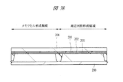
図38に示すように、メモリセル形成領域および周辺回路形成領域を含む半導体基板200上に、例えば熱酸化法を使用してゲート絶縁膜201を形成し、このゲート絶縁膜201上に、例えばCVD(Chemical Vapor Deposition)法を使用して電荷蓄積膜202を形成する。そして、例えばCVD法を使用して、電位障壁膜203を形成し、この電位障壁膜203上に、例えばCVD法を使用してポリシリコン膜204を形成する。ゲート絶縁膜201および電位障壁膜203は、例えば酸化シリコン膜から形成され、電荷蓄積膜202は、例えば窒化シリコン膜から形成される。
As shown in FIG. 38, a gate
次に、図39に示すように、フォトリソグラフィ技術およびエッチング技術を使用することにより、メモリセル形成領域にMONOS型トランジスタのゲート電極205を形成する。このとき、ゲート電極205と半導体基板200の間には、ゲート絶縁膜(第1電位障壁膜)201、電荷蓄積膜202および電位障壁膜(第2電位障壁膜)203が形成されている。続いて、図40に示すように、ゲート電極205を形成した半導体基板200上に、例えば熱酸化法を用いてゲート絶縁膜206を形成し、このゲート絶縁膜206上にポリシリコン膜207を形成する。
Next, as shown in FIG. 39, the
そして、フォトリソグラフィ技術およびエッチング技術を用いてポリシリコン膜207およびゲート絶縁膜206を加工することにより、図41に示すように、周辺回路形成領域にMISFETのゲート電極208を形成する。このゲート電極208と半導体基板200との間には、ゲート絶縁膜206が形成されている。このとき、図41に示すように、MONOS型トランジスタのゲート電極205の側壁にエッチング残渣209が残存する。
Then, by processing the
次に、図42に示すように、レジストパターン210を形成する。レジストパターン210は、周辺回路形成領域を覆い、メモリセル形成領域を露出するようにパターニングされている。そして、レジストパターン210をマスクにしたエッチングにより、ゲート電極205の側壁に形成されているエッチング残渣209を除去する。続いて、図43に示すように、レジストパターン210を除去することにより、メモリセル形成領域にMONOS型トランジスタのゲート電極205を形成し、周辺回路形成領域にMISFETのゲート電極208を形成することができる。
Next, as shown in FIG. 42, a
この第1技術によれば、以下に示す問題点がある。すなわち、図40に示すように、メモリセル形成領域にMONOS型トランジスタのゲート電極205を形成した後、半導体基板200上の全面にゲート絶縁膜206を形成している。このとき、ゲート電極205を構成するポリシリコン膜も酸化される。特に、電位障壁膜203と接する境界近傍領域であって、ゲート電極205の側壁端部において酸化が進行する。これにより、ゲート電極205の端部にバーズビーグが形成される。さらに、ゲート絶縁膜201と接する半導体基板200にもバーズビークが生じ、端部におけるゲート絶縁膜201の膜厚が厚くなる。ゲート絶縁膜201は、電荷蓄積膜202への電子の注入および注出の際のトンネル絶縁膜として機能するものである。したがって、バーズビークの形成によってゲート絶縁膜201の膜厚が厚くなると、トンネル現象が起こりづらくなり、電荷蓄積膜202への電子の注入および注出が起きづらくなる。すると、情報の書き込みあるいは情報の消去が遅くなり、MONOS型トランジスタの特性が劣化する問題点が生じる。例えば、トンネル絶縁膜となるゲート絶縁膜201にバーズビークが生じると、バーズビークが生じた領域でゲート絶縁膜201の膜厚が厚くなるため、情報の消去がされにくくなる。このことから、消去動作によってしきい値電圧が所定レベルまで低下せず、書き換えを繰り返すことで読み出し電流が減少する問題点が生じる。さらに、ゲート電極205を微細化すると、ゲート電極205全体に対して、バーズビークが形成される領域の割合が増加するので、ゲート絶縁膜201の膜厚制御性が悪化する。このため、読み出し電流の低下や短チャネル特性の劣化が生じる。
The first technique has the following problems. That is, as shown in FIG. 40, after forming the
また、第1技術では、図41に示すように、ゲート電極205の側壁にエッチング残渣209が形成されるため、このエッチング残渣209を除去する必要がある。エッチング残渣209の除去は、例えばドライエッチングによって実施されるが、このドライエッチングにより、ゲート電極205の端部にエッチングダメージが発生するおそれがある。このエッチングダメージを緩和するため、例えば、ゲート電極205の表面を予め酸化するライト酸化工程などが必要となり、さらに、ゲート絶縁膜201の端部にバーズビークが生じやすくなる。
Further, in the first technique, as shown in FIG. 41, an
このように、MONOS型トランジスタのゲート電極205を、周辺回路を構成するMISFETのゲート電極208よりも先に形成すると、上述した問題点が発生する。そこで、第2技術として、周辺回路を構成するMISFETのゲート電極を先に形成し、続いてMONOS型トランジスタのゲート電極を形成する技術がある。この技術について図面を参照しながら説明する。
As described above, if the
図44に示すように、メモリセル形成領域および周辺回路形成領域を含む半導体基板300上に、例えば熱酸化法を使用して酸化シリコン膜よりなるゲート絶縁膜301を形成し、このゲート絶縁膜301上に、例えばCVD(Chemical Vapor Deposition)法を使用してポリシリコン膜302を形成する。
As shown in FIG. 44, a
次に、図45に示すように、フォトリソグラフィ技術およびエッチング技術を使用することにより、ポリシリコン膜302を加工して、周辺回路形成領域にゲート電極303を形成する。
Next, as shown in FIG. 45, by using a photolithography technique and an etching technique, the
続いて、図46に示すように、ゲート電極303を形成した半導体基板300の全面にゲート絶縁膜304、電荷蓄積膜305および電位障壁膜306を形成する。そして、電位障壁膜306上にポリシリコン膜307を形成する。その後、図47に示すように、フォトリソグラフィ技術およびエッチング技術を使用して、メモリセル形成領域にゲート電極308を形成する。このとき、周辺回路形成領域に形成されているゲート電極303の側壁には、エッチング残渣309が残存する。
Subsequently, as shown in FIG. 46, a
次に、図48に示すように、レジストパターン310を形成する。このレジストパターン310は、メモリセル形成領域を覆い、周辺回路形成領域を露出するようにパターニングされている。そして、このレジストパターン310をマスクにしたエッチングにより、ゲート電極303の側壁に形成されているエッチング残渣309を除去する。その後、図49に示すように、レジストパターン310を除去することにより、メモリセル形成領域にゲート電極308を形成し、周辺回路形成領域にゲート電極303を形成することができる。
Next, as shown in FIG. 48, a resist
この第2技術によれば、MONOS型トランジスタのゲート電極308を、周辺回路用MISFETのゲート電極303よりも後の工程で形成するため、周辺回路用のゲート絶縁膜301を形成する際、MONOS型トランジスタのゲート絶縁膜304が酸化されることはなく、MONOS型トランジスタにおいて、バーズビークの問題は発生しない。
According to the second technique, since the
しかし、周辺回路用MISFETのゲート電極303を、MONOS型トランジスタのゲート電極308よりも先に形成するため、以下に示す問題点が発生する。
However, since the
図46に示すように、周辺回路形成領域にMISFETのゲート電極303を形成した後、半導体基板300上の全面にゲート絶縁膜304を形成している。このため、ゲート絶縁膜304を形成する際、ゲート電極303の端部が酸化され、ゲート絶縁膜301の端部でバーズビークが発生する。ゲート絶縁膜301の端部でバーズビークが発生すると、ゲート絶縁膜301の端部の膜厚が厚くなる。ゲート絶縁膜301の端部の膜厚が厚くなると、周辺回路用MISFETのソース領域とドレイン領域との間を流れる電流が少なくなる。すなわち、この電流の大きさは、ゲート絶縁膜301の膜厚に反比例するため、ゲート絶縁膜301が厚くなると、ソース領域とドレイン領域との間を流れる電流を確保できなくなり、周辺回路用MISFETの特性が劣化する。さらに、周辺回路用MISFET(特に低耐圧MISFET)を微細化すると、ゲート電極303のゲート長が短くなるため、しきい値電圧が低下する短チャネル特性が顕在化する。この短チャネル特性は、ゲート絶縁膜301が薄いほど改善されるが、バーズビークによってゲート絶縁膜301の膜厚が厚くなると、短チャネル特性がより顕在化することになり、周辺回路用MISFETの特性が劣化する。
As shown in FIG. 46, after forming the
また、第2技術では、図47に示すように、ゲート電極303の側壁にエッチング残渣309が形成されるため、このエッチング残渣309を除去する必要がある。エッチング残渣309の除去は、例えばドライエッチングによって実施されるが、このドライエッチングにより、ゲート電極303の端部にエッチングダメージが発生するおそれがある。
In the second technique, as shown in FIG. 47, an
さらに、第2技術では、図45に示すように、周辺回路用MISFET(低耐圧MISFET)のゲート絶縁膜301として、3nm程度の酸化シリコン膜を用いており、ゲート電極303加工後の周辺回路形成領域(低耐圧MISFET形成領域)には、3nm未満の酸化シリコン膜しか残存していない(図45では図示せず)。ここで、図47に示すように、MONOS型トランジスタのゲート電極308を加工する際、周辺回路形成領域に残存するポリシリコン膜307、電位障壁膜306、電荷蓄積膜305およびゲート絶縁膜304は除去される。このとき、窒化シリコン膜よりなる電荷蓄積膜305を除去する際、電荷蓄積膜305の下部に存在する酸化シリコン膜(3nm未満の酸化シリコン膜とゲート絶縁膜304を合わせた膜)の膜厚が薄く、窒化シリコン膜を除去する際に使用する熱リン酸にゲート電極303のエッジなどがさらされてゲート欠陥密度が増加する問題や半導体基板300がえぐれることによる不良を招くおそれがある。
Furthermore, in the second technique, as shown in FIG. 45, a silicon oxide film of about 3 nm is used as the
以上述べたように、第1技術あるいは第2技術のいずれを用いても、2種類のゲート電極のうち、先に形成するゲート電極に問題が生じることがわかる。 As described above, it can be seen that there is a problem with the gate electrode formed first, out of the two types of gate electrodes, using either the first technique or the second technique.
本発明の目的は、第1MISFETのゲート電極と第2MISFETのゲート電極とを別工程で形成する半導体装置の製造技術において、第1MISFETおよび第2MISFETの信頼性向上を図ることができる技術を提供することにある。 An object of the present invention is to provide a technique capable of improving the reliability of a first MISFET and a second MISFET in a manufacturing technique of a semiconductor device in which a gate electrode of a first MISFET and a gate electrode of a second MISFET are formed in separate processes. It is in.
本発明の前記ならびにその他の目的と新規な特徴は、本明細書の記述および添付図面から明らかになるであろう。 The above and other objects and novel features of the present invention will be apparent from the description of this specification and the accompanying drawings.
本願において開示される発明のうち、代表的なものの概要を簡単に説明すれば、次のとおりである。 Of the inventions disclosed in the present application, the outline of typical ones will be briefly described as follows.
本発明による半導体装置の製造方法は、半導体基板の第1領域上に第1MISFETを形成し、前記半導体基板の第2領域上に第2MISFETを形成する半導体装置の製造方法に関するものである。そして、(a)前記第1領域および前記第2領域を含む前記半導体基板上に第1絶縁膜を形成する工程と、(b)前記第1絶縁膜上に第1導体膜を形成する工程と、(c)前記第2領域上に形成されている前記第1導体膜および前記第1絶縁膜を除去する工程とを備える。また、(d)前記(c)工程後、前記第2領域を含む前記半導体基板上および前記第1領域を含む前記第1導体膜上に第2絶縁膜を形成する工程と、
(e)前記第2絶縁膜上に第2導体膜を形成する工程と、(f)前記第2導体膜および前記第2絶縁膜をパターニングすることにより、前記第2領域に前記第2MISFETの第2ゲート電極を形成する工程とを備える。さらに、(g)前記(f)工程後、前記第1領域に形成されている前記第1導体膜および前記第1絶縁膜をパターニングすることにより、前記第1領域に前記第1MISFETの第1ゲート電極を形成する工程とを備えるものである。
A method for manufacturing a semiconductor device according to the present invention relates to a method for manufacturing a semiconductor device in which a first MISFET is formed on a first region of a semiconductor substrate and a second MISFET is formed on a second region of the semiconductor substrate. And (a) forming a first insulating film on the semiconductor substrate including the first region and the second region; and (b) forming a first conductor film on the first insulating film. (C) removing the first conductor film and the first insulating film formed on the second region. (D) after the step (c), forming a second insulating film on the semiconductor substrate including the second region and on the first conductor film including the first region;
(E) forming a second conductor film on the second insulating film; and (f) patterning the second conductor film and the second insulating film to form a second MISFET in the second region. Forming two gate electrodes. Further, (g) after the step (f), the first gate of the first MISFET is formed in the first region by patterning the first conductor film and the first insulating film formed in the first region. Forming an electrode.
本願において開示される発明のうち、代表的なものによって得られる効果を簡単に説明すれば以下のとおりである。 Among the inventions disclosed in the present application, effects obtained by typical ones will be briefly described as follows.
第1MISFETの第1ゲート電極と第2MISFETの第2ゲート電極を加工する前に、第1ゲート電極を形成するための導体膜と第2ゲート電極を形成するための導体膜を形成する。そして、これらの導体膜を形成した後、第1ゲート電極および第2ゲート電極を加工するので、第1MISFETおよび第2MISFETの信頼性向上を図ることができる。 Before processing the first gate electrode of the first MISFET and the second gate electrode of the second MISFET, a conductor film for forming the first gate electrode and a conductor film for forming the second gate electrode are formed. Since the first gate electrode and the second gate electrode are processed after these conductor films are formed, the reliability of the first MISFET and the second MISFET can be improved.
以下の実施の形態においては便宜上その必要があるときは、複数のセクションまたは実施の形態に分割して説明するが、特に明示した場合を除き、それらはお互いに無関係なものではなく、一方は他方の一部または全部の変形例、詳細、補足説明等の関係にある。 In the following embodiments, when it is necessary for the sake of convenience, the description will be divided into a plurality of sections or embodiments. However, unless otherwise specified, they are not irrelevant to each other. There are some or all of the modifications, details, supplementary explanations, and the like.
また、以下の実施の形態において、要素の数等(個数、数値、量、範囲等を含む)に言及する場合、特に明示した場合および原理的に明らかに特定の数に限定される場合等を除き、その特定の数に限定されるものではなく、特定の数以上でも以下でもよい。 Further, in the following embodiments, when referring to the number of elements (including the number, numerical value, quantity, range, etc.), especially when clearly indicated and when clearly limited to a specific number in principle, etc. Except, it is not limited to the specific number, and may be more or less than the specific number.
さらに、以下の実施の形態において、その構成要素(要素ステップ等も含む)は、特に明示した場合および原理的に明らかに必須であると考えられる場合等を除き、必ずしも必須のものではないことは言うまでもない。 Further, in the following embodiments, the constituent elements (including element steps and the like) are not necessarily indispensable unless otherwise specified and apparently essential in principle. Needless to say.
同様に、以下の実施の形態において、構成要素等の形状、位置関係等に言及するときは、特に明示した場合および原理的に明らかにそうではないと考えられる場合等を除き、実質的にその形状等に近似または類似するもの等を含むものとする。このことは、上記数値および範囲についても同様である。 Similarly, in the following embodiments, when referring to the shape, positional relationship, etc., of components, etc., unless otherwise specified, and in principle, it is considered that this is not clearly the case, it is substantially the same. Including those that are approximate or similar to the shape. The same applies to the above numerical values and ranges.
また、実施の形態を説明するための全図において、同一の部材には原則として同一の符号を付し、その繰り返しの説明は省略する。 In all the drawings for explaining the embodiments, the same members are denoted by the same reference symbols in principle, and the repeated explanation thereof is omitted.
以下、本発明の実施の形態を図面に基づいて詳細に説明する。 Hereinafter, embodiments of the present invention will be described in detail with reference to the drawings.
(実施の形態1)
本実施の形態1は、相対的に低い電圧で駆動する低耐圧MISFET(Metal Insulator Semiconductor)と、高電圧駆動を可能とするために相対的に高い電圧で駆動する高耐圧MISFETとを有する半導体装置であって、書き換え可能な不揮発性メモリセルを含む半導体装置およびその製造方法に本発明を適用したものである。MISFETにおいて、耐圧とは、MISFETを構成するソース領域と半導体基板(ウェル)やドレイン領域と半導体基板(ウェル)との境界に生じるpn接合耐圧や、ゲート絶縁膜の絶縁耐圧をいい、本実施の形態1では、相対的に耐圧の高い高耐圧MISFETと相対的に耐圧の低い低耐圧MISFETが半導体基板に形成されている。
(Embodiment 1)
The first embodiment is a semiconductor device having a low breakdown voltage MISFET (Metal Insulator Semiconductor) driven at a relatively low voltage and a high breakdown voltage MISFET driven at a relatively high voltage to enable high voltage drive. The present invention is applied to a semiconductor device including a rewritable nonvolatile memory cell and a manufacturing method thereof. In the MISFET, the breakdown voltage refers to a pn junction breakdown voltage generated at the boundary between the source region and the semiconductor substrate (well) or the drain region and the semiconductor substrate (well) constituting the MISFET, or a breakdown voltage of the gate insulating film. In the first mode, a high breakdown voltage MISFET having a relatively high breakdown voltage and a low breakdown voltage MISFET having a relatively low breakdown voltage are formed on a semiconductor substrate.
図1から図3を参照して実施の形態における半導体装置の構成について説明する。 The structure of the semiconductor device in the embodiment will be described with reference to FIGS.
図1は、チップ(半導体基板)1に形成されたそれぞれの素子のレイアウト構成を示した上面図である。図1において、チップ1は、CPU(Central Processing Unit)2、ROM(Read Only Memory)3、RAM(Random Access Memory)4、EEPROM(Electrically Erasable Programmable Read Only Memory)5、アナログ回路6、静電保護回路7a〜7gを有している。
FIG. 1 is a top view showing a layout configuration of each element formed on a chip (semiconductor substrate) 1. In FIG. 1, a chip 1 includes a CPU (Central Processing Unit) 2, a ROM (Read Only Memory) 3, a RAM (Random Access Memory) 4, an EEPROM (Electrically Erasable Programmable Read Only Memory) 5, an
CPU(回路)2は、中央演算処理装置とも呼ばれ、コンピュータなどの心臓部にあたる。このCPU2は、記憶装置から命令を読み出して解読し、それに基づいて多種多様な演算や制御を行なうものであり、処理の高速性が要求される。したがって、CPU2を構成しているMISFETには、チップ1に形成されている素子の中で、相対的に大きな電流駆動力が必要とされる。すなわち低耐圧MISFETで形成される。
The CPU (circuit) 2 is also called a central processing unit and is the heart of a computer or the like. The
ROM(回路)3は、記憶情報が固定され変更できないメモリで、読み出し専用メモリと呼ばれる。ROM3の構成には、MISFETを直列接続したNAND型と、MISFETを並列接続したNOR型がある。NAND型は、集積密度重視であるのに対し、NOR型は、動作速度重視の目的で使用されることが多い。このROM3も動作の高速性が要求されるため、ROM3を構成しているMISFETには、相対的に大きな電流駆動力が必要とされる。すなわち低耐圧MISFETで形成される。
A ROM (circuit) 3 is a memory in which stored information is fixed and cannot be changed, and is called a read-only memory. The configuration of the
RAM(回路)4は、記憶情報をランダムに、すなわち随時記憶されている記憶情報を読み出したり、記憶情報を新たに書き込んだりすることができるメモリであり、随時書き込み読み出しができるメモリとも呼ばれる。ICメモリとしてのRAMには、ダイナミック回路を用いたDRAM(Dynamic RAM)とスタティック回路を用いたSRAM(Static RAM)の2種類がある。DRAMは、記憶保持動作が必要な随時書き込み読み出しメモリであり、SRAMは、記憶保持動作が不要な随時書き込み読み出しメモリである。これらRAM3も動作の高速性が要求されるため、RAM3を構成しているMISFETには、相対的に大きな電流駆動力が必要とされている。すなわち低耐圧MISFETで形成される。
The RAM (circuit) 4 is a memory that can read stored information at random, that is, read stored information at any time, or write new stored information, and is also called a memory that can be written and read at any time. There are two types of RAM as an IC memory: DRAM (Dynamic RAM) using a dynamic circuit and SRAM (Static RAM) using a static circuit. DRAM is an occasional writing / reading memory that requires a memory holding operation, and SRAM is an occasional writing / reading memory that does not require a memory holding operation. Since these
EEPROM5は、書き込み動作および消去動作とも電気的に書き換え可能な不揮発性メモリの一種であり、電気的消去可能なプログラマブル読み出し専用メモリとも呼ばれる。このEEPROM5のメモリセルは、記憶(メモリ)用の例えばMONOS(Metal Oxide Nitride Oxide Semiconductor)型トランジスタやMNOS(Metal Nitride Oxide Semiconductor)型トランジスタから構成される。EEPROM5の書き込み動作および消去動作には、例えばファウラーノルドハイム型トンネル現象を利用する。なお、ホットエレクトロンやホットホールを用いて書き込み動作や消去動作させることも可能である。
The
EEPROM5の書き込み動作時などには、記憶用のMONOS型トランジスタに高い電位差(12V程度)が生じるため、記憶用のMONOS型トランジスタとして、相対的に高耐圧のトランジスタが必要とされる。
A high potential difference (about 12 V) is generated in the memory MONOS transistor during the writing operation of the
アナログ回路6は、時間的に連続して変化する電圧や電流の信号、すなわちアナログ信号を扱う回路であり、例えば増幅回路、変換回路、変調回路、発振回路、電源回路などから構成されている。これらアナログ回路6は、チップ1に形成された素子の中で、相対的に高耐圧の高耐圧MISFETが使用される。
The
静電保護回路7a〜7gは、素子や絶縁膜などが帯電電荷の放電により生じた電圧や発熱で、内部回路が破壊されることを防止するために外部端子に設けられた回路である。帯電電荷としては、例えば人体、物体などに蓄積された静電気によるものがある。なお、静電保護回路7a、7cは、入出力端子に設けられ、静電保護回路7bは、モニタ端子に設けられている。また、静電保護回路7dは、Vss端子に設けられ、静電保護回路7eは、CLK(クロック)端子に設けられている。さらに静電保護回路7fは、RST(リセット)端子に設けられ、静電保護回路7gは、Vcc端子に設けられている。これら静電保護回路7a、7c〜7gには、高電圧が印加されるため、チップ1に形成された素子の中で、相対的に高耐圧の高耐圧MISFETが使用される。
The
次に、図1に示したEEPROM5の内部構成の一例を図2に示す。図2において、EEPROM5は、メモリアレイ10とメモリアレイを駆動するための駆動回路としてメモリアレイ10の直接周辺回路部11および間接周辺回路部12を有している。
Next, FIG. 2 shows an example of the internal configuration of the
メモリアレイ10は、EEPROM5の記憶部にあたり、メモリセルが縦と横の2次元上に多数配置されている。メモリセルは、1ビットの単位情報を記憶するための回路であり、記憶部であるMONOS型トランジスタより構成されている。
The
駆動回路は、メモリアレイ10を駆動するための回路であり、直接周辺回路部11としては、例えば電源電圧から数倍の電圧を生成する昇圧回路、昇圧用クロック発生回路、電圧クランプ回路、行や列を選択するカラムデコーダやロウデコーダ、カラムラッチ回路およびWELL制御回路などを有している。これら直接周辺回路部11を構成するMISFETは、チップ1に形成されている素子の中で、相対的に高耐圧を必要とする高耐圧MISFETより形成されている。
The drive circuit is a circuit for driving the
また、間接周辺回路部12としてはメモリアレイの書き換え制御回路として形成されており、設定回路、通常用書き換えクロック生成回路、高速用書き換えクロック生成回路および書き換えタイミング制御回路等を有する回路からなる。これら間接周辺回路部12を構成するMISFETは、チップ1に形成されている素子の中で、相対的に低い電圧で駆動し、高速動作が可能な低耐圧MISFETより形成されている。
The indirect
続いて、図3にチップ1上に形成されたMONOS型トランジスタQ1、低耐圧MISFETQ2、高耐圧MISFETQ3および容量素子Cの断面図を示す。図3において、メモリセル形成領域は、EEPROM(書き換え可能な不揮発性メモリ)5内の複数のメモリセル形成領域を示しており、MONOS型トランジスタQ1が形成されている。低耐圧MISFET形成領域は、高速動作を可能とするために大きな電流駆動力を必要とする低耐圧MISFETQ2が形成されている領域を示している。このような低耐圧MISFETQ2が形成される領域としては、例えばCPU2やRAM4の形成領域などが考えられる。この低耐圧MISFETは、例えば、1.5V程度の電源電圧で動作する。また、高耐圧MISFET形成領域は、高耐圧MISFETQ3が形成されている領域を示しており、例えばアナログ回路6の形成領域、EEPROM5内の駆動回路(デコーダなど)が形成されている領域などが考えられる。この高耐圧MISFETQ3は、例えば、5V程度の電源電圧で動作する。容量素子形成領域には、回路を構成する容量素子が形成されており、例えば、容量素子は、PIP(Polysilicon Insulator Polysilicon)で形成されている。
Next, FIG. 3 shows a cross-sectional view of the MONOS transistor Q 1 , the low breakdown voltage MISFET Q 2 , the high breakdown voltage MISFET Q 3 and the capacitor C formed on the chip 1. 3, the memory cell formation region, EEPROM shows a plurality of memory cell formation region of the (rewritable nonvolatile memory) 5, MONOS type transistor Q 1 is formed. Low breakdown voltage MISFET formation region is a region where low breakdown voltage MISFET Q 2 is formed which requires a large current driving force in order to enable high-speed operation. Such regions low breakdown voltage MISFET Q 2 is formed, for example, forming regions of the CPU2 or RAM4 is considered. This low withstand voltage MISFET operates with a power supply voltage of about 1.5V, for example. The high breakdown voltage MISFET formation region is a region where high-voltage MISFET Q 3 is formed, for example, formation region of the
図3に示すように、半導体基板20には、素子を分離する素子分離領域21が形成されており、素子分離領域21によって分離された活性領域が、それぞれメモリセル形成領域低耐圧MISFET形成領域および高耐圧MISFET形成領域となっている。メモリセル形成領域、低耐圧MISFET形成領域および高耐圧MISFET形成領域の半導体基板20内には、ウェル分離層となるn型半導体領域22が形成されており、このn型半導体領域22上にウェルが形成されている。例えば、メモリセル形成領域においては、n型半導体領域22上にp型ウェル23が形成されている。同様に、低耐圧MISFET形成領域には、n型半導体領域22上にp型ウェル24が形成されており、高耐圧MISFET形成領域には、n型半導体領域22上にp型ウェル25が形成されている。メモリセル形成領域に形成されているp型ウェル23と高耐圧MISFET形成領域に形成されているp型ウェル25とは同一工程で形成され、同様の不純物濃度を有している。これは、メモリセルと高耐圧MISFETに印加される電圧などの条件が類似しているためである。これに対し、低耐圧MISFETに印加される電圧などの条件は高耐圧MISFETと異なるため、低耐圧MISFET形成領域に形成されるp型ウェル24の不純物濃度は、p型ウェル23およびp型ウェル25と異なっている。
As shown in FIG. 3, an
なお、本実施の形態1では、低耐圧MISFET形成領域および高耐圧MISFET形成領域に形成されているMISFETとしてnチャネル型MISFETを図示して説明するが、それぞれの領域にはpチャネル型MISFETも形成されている。 In the first embodiment, an n-channel type MISFET is illustrated and described as a MISFET formed in the low breakdown voltage MISFET formation region and the high breakdown voltage MISFET formation region, but a p-channel type MISFET is also formed in each region. Has been.
次に、図3に示すMONOS型トランジスタQ1の構成について説明する。 Next, description will be given of a configuration of the MONOS transistor Q 1 shown in FIG.
まず、メモリセル形成領域内に形成されたMONOS型トランジスタQ1は、以下に示す構成をしている。すなわち、半導体基板20内に形成されたp型ウェル23上にゲート絶縁膜26が形成されており、このゲート絶縁膜26上に電荷蓄積膜27が形成されている。そして、この電荷蓄積膜27上に絶縁膜(電位障壁膜)28が形成され、絶縁膜28上に導電膜からなるゲート電極44が形成されている。ゲート電極44は、低抵抗化を図るため、例えばポリシリコン膜29とコバルトシリサイド膜56の積層膜から構成されており、ゲート電極44の両側の側壁にはLDD(Lightly Doped Drain)構造を形成するため、例えば絶縁膜からなるサイドウォール51が形成されている。
First, MONOS type transistor Q 1 formed in the memory cell forming region has the structure shown below. That is, the
サイドウォール51下の半導体基板20内には、半導体領域として、低濃度n型不純物拡散領域48および高濃度n型不純物拡散領域53が形成されている。また、ゲート絶縁膜26の直下のp型ウェル23内には、n型半導体領域よりなるチャネル形成領域が形成されている。
In the
上記のように構成されたMONOS型トランジスタQ1において、ゲート絶縁膜26は、例えば酸化シリコン膜より形成されており、トンネル絶縁膜としての機能も有する。例えば、このMONOS型トランジスタQ1は、半導体基板20からゲート絶縁膜26を介して電荷蓄積膜27に電子を注入したり、電荷蓄積膜27に蓄積した電子を半導体基板20へ放出したりしてデータの記憶や消去を行なうため、ゲート絶縁膜26は、トンネル絶縁膜として機能する。
In the MONOS transistor Q 1 that is configured as described above, the
電荷蓄積膜27は、データ記憶に寄与する電荷を蓄積するために設けられた膜であり、例えば窒化シリコン膜より形成されている。
The
従来、電荷蓄積膜27としてポリシリコン膜が主に使用されてきたが、電荷蓄積膜27としてポリシリコン膜を使用した場合、電荷蓄積膜27を取り囲む酸化膜のどこか一部に欠陥があると、電荷蓄積膜27が導体であるため、異常リークにより電荷蓄積膜27に蓄積された電荷がすべて抜けてしまうことが起こりうる。
Conventionally, a polysilicon film has been mainly used as the
そこで、上述したように電荷蓄積膜27として、絶縁体である窒化シリコン膜が使用されてきている。この場合、データ記憶に寄与する電荷は、窒化シリコン膜中に存在する離散的なトラップ準位(捕獲準位)に蓄積される。したがって、電荷蓄積膜27を取り巻く酸化膜中の一部に欠陥が生じても、電荷は電荷蓄積膜27の離散的なトラップ準位に蓄積されているため、すべての電荷が電荷蓄積膜27から抜け出てしまうことがない。このため、データ保持の信頼性向上を図ることができる。
Therefore, as described above, a silicon nitride film that is an insulator has been used as the
このような理由から、電荷蓄積膜27として、窒化シリコン膜に限らず、離散的なトラップ準位を含むような膜を使用することにより、データ保持の信頼性向上を図ることができる。
For this reason, not only the silicon nitride film but also a film including discrete trap levels can be used as the
サイドウォール51は、MONOS型トランジスタQ1の半導体領域であるソース領域およびドレイン領域をLDD構造にするために形成されたものである。すなわち、MONOS型トランジスタQ1のソース領域およびドレイン領域は、低濃度n型不純物拡散領域48および高濃度n型不純物拡散領域53より形成されている。このとき、サイドウォール51下のソース領域およびドレイン領域を低濃度n型不純物拡散領域48とすることで、ゲート電極44の端部下における電界集中を抑制することができるようにしている。
次に、図3に示す低耐圧MISFETQ2の構成について説明する。低耐圧MISFETQ2は、半導体基板20内に形成されたp型ウェル24上にゲート絶縁膜36が形成されており、このゲート絶縁膜36上にゲート電極39が形成されている。ゲート絶縁膜36は、例えば酸化シリコン膜から形成され、ゲート電極39は、低抵抗化のため、例えばポリシリコン膜37およびコバルトシリサイド膜56の積層膜から形成されている。
Next, description will be given of a configuration of the low-voltage MISFET Q 2 shown in FIG. In the low breakdown voltage MISFET Q 2 , a
ゲート電極39の両側の側壁には、サイドウォール52が形成されており、このサイドウォール52下の半導体基板20内には、半導体領域として、低濃度n型不純物拡散領域49および高濃度n型不純物拡散領域54が形成されている。また、ゲート絶縁膜36の直下のp型ウェル24内には、p型半導体領域よりなるチャネル形成領域が形成されている。
続いて、図3に示す高耐圧MISFETQ3の構成について説明する。高耐圧MISFETQ3は、半導体基板20内に形成されたp型ウェル25上にゲート絶縁膜34が形成されており、このゲート絶縁膜34上にゲート電極40が形成されている。ゲート絶縁膜34は、例えば酸化シリコン膜から形成され、ゲート電極40は、低抵抗化のため、例えばポリシリコン膜37とコバルトシリサイド膜56との積層膜から形成されている。
Next, a configuration of the high-voltage MISFET Q 3 shown in FIG. In the high voltage MISFET Q 3 , a
ゲート電極40の両側の側壁には、サイドウォール51が形成されており、このサイドウォール51下の半導体基板20内には、半導体領域として、低濃度n型不純物拡散領域50および高濃度n型不純物拡散領域55が形成されている。また、ゲート絶縁膜34直下のp型ウェル25内には、p型半導体領域よりなるチャネル形成領域が形成されている。
次に、低耐圧MISFETQ2と高耐圧MISFETQ3の相違点について説明する。まず、高耐圧MISFETQ3のサイドウォール51の幅は、低耐圧MISFETQ2のサイドウォール52の幅に比べて広くなっている。高耐圧MISFETQ3には、動作時に比較的高い電位差(5V程度)が印加されるため、サイドウォール51の幅を相対的に広げてソース・ドレイン領域と半導体基板(p型ウェル25)間のpn接合耐圧を向上させる必要があるからである。一方、低耐圧MISFETQ2には、動作時に比較的低い電位差(1.5V程度)しか印加されないため、サイドウォール52の幅を相対的に狭くして動作の高速性向上を図っている。
Next, the difference will be described of the low voltage MISFET Q 2 and the high-voltage MISFET Q 3. First, the width of the high-voltage MISFET Q 3 of the
また、高耐圧MISFETQ3におけるゲート電極40のゲート長は、低耐圧MISFETQ2におけるゲート電極39のゲート長に比べて長くなっている。低耐圧MISFETQ2では、ゲート電極39のゲート長を短くすることにより、ソース領域とドレイン領域との間の抵抗を減らし、電流駆動力を向上させる必要があるからである。一方、高耐圧MISFETQ3では、比較的高い電位が印加されるため、ゲート長を短くすると、ソース領域とドレイン領域との間でパンチスルーが発生してしまうからである。
The gate length of the
さらに、高耐圧MISFETQ3は、低耐圧MISFETQ2に比べて高い電圧が印加されるため、そのゲート絶縁膜34は、低耐圧MISFETQ2のゲート絶縁膜36に比べて厚くなっている。これにより、高耐圧MISFETQ3のゲート絶縁膜34の絶縁耐性を向上させている。
Further, the high-voltage MISFET Q 3, since the higher voltage than the low breakdown voltage MISFET Q 2 is applied, a
続いて、図3に示す容量素子Cの構成について説明する。容量素子Cは、例えばポリシリコン膜から形成されている下部電極33を有しており、この下部電極33上に容量絶縁膜が形成されている。容量絶縁膜は、積層化された絶縁膜から形成され、例えば酸化シリコン膜30、窒化シリコン膜31および酸化シリコン膜41の積層膜から形成されている。容量絶縁膜上には、例えばポリシリコン膜からなる上部電極42が形成されている。この下部電極33および上部電極42の表面にはコバルトシリサイド膜56が形成されている。容量絶縁膜の膜厚および上部電極42と下部電極33の面積を調整することにより、所望の容量値を有する容量素子Cが形成されている。
Next, the configuration of the capacitive element C illustrated in FIG. 3 will be described. The capacitive element C has a
このように構成されたMONOS型トランジスタQ1、低耐圧MISFETQ2、高耐圧MISFETQ3および容量素子C上には、窒化シリコン膜57および酸化シリコン膜58よりなる層間絶縁膜が形成されている。そして、層間絶縁膜には、コンタクトホール59が形成されており、このコンタクトホール59を埋め込むようにプラグ60が形成されている。プラグ60は、例えばチタン/窒化チタン膜よりなるバリア膜とタングステン膜から形成されている。プラグ60を形成した層間絶縁膜上には、例えばアルミニウム膜あるいはアルミニウム合金膜よりなる配線61が形成されている。
On the thus configured MONOS transistor Q 1 , low withstand voltage MISFET Q 2 , high withstand voltage MISFET Q 3, and capacitive element C, an interlayer insulating film made of a
本実施の形態1における半導体装置は上記のように構成されており、次に、本実施の形態1の特徴構成について説明する。図3において、本発明の特徴の1つは、MONOS型トランジスタQ1、低耐圧MISFETQ2および高耐圧MISFETQ3において、バーズビークが抑制されている点である。 The semiconductor device according to the first embodiment is configured as described above. Next, the characteristic configuration of the first embodiment will be described. In FIG. 3, one of the features of the present invention is that bird's beak is suppressed in the MONOS transistor Q 1 , the low breakdown voltage MISFET Q 2 and the high breakdown voltage MISFET Q 3 .
従来の製造方法では、MONOS型トランジスタのゲート電極と、周辺回路用MISFET(低耐圧MISFETおよび高耐圧MISFET)のゲート電極は、いずれか一方のゲート電極を加工してから、ゲート絶縁膜および導体膜を堆積し、その後、もう一方のゲート電極を加工することにより形成されていた。したがって、先に加工されたゲート電極は、もう一方のゲート絶縁膜を形成する際、表面が酸化される。特に、先に加工されたゲート電極と半導体基板の間にバーズビークが生じ、端部におけるゲート絶縁膜の膜厚が厚くなる。例えば、先に形成されたゲート電極がMONOS型トランジスタのものである場合、MONOS型トランジスタのゲート絶縁膜は、電荷蓄積膜への電子の注入および注出の際のトンネル絶縁膜として機能するものである。したがって、バーズビークの形成によってゲート絶縁膜の膜厚が厚くなると、トンネル現象が起こりづらくなり、電荷蓄積膜への電子の注入および注出が起きづらくなる。すると、情報の書き込みあるいは情報の消去が遅くなり、MONOS型トランジスタの特性が劣化する問題点が生じる。一方、先に形成されたゲート電極が周辺回路用MISFETのものである場合も、バーズビークの発生により特性が劣化する。 In the conventional manufacturing method, the gate electrode of the MONOS transistor and the gate electrode of the peripheral circuit MISFET (low withstand voltage MISFET and high withstand voltage MISFET) are processed after either gate electrode is processed, and then the gate insulating film and the conductor film And then processing the other gate electrode. Therefore, the surface of the previously processed gate electrode is oxidized when the other gate insulating film is formed. In particular, a bird's beak is generated between the gate electrode processed previously and the semiconductor substrate, and the film thickness of the gate insulating film at the end increases. For example, when the previously formed gate electrode is of a MONOS type transistor, the gate insulating film of the MONOS type transistor functions as a tunnel insulating film when electrons are injected into and extracted from the charge storage film. is there. Therefore, when the gate insulating film is thickened due to the formation of bird's beaks, the tunnel phenomenon is less likely to occur, and the injection and extraction of electrons into the charge storage film is difficult to occur. As a result, writing of information or erasing of information is delayed, causing a problem that characteristics of the MONOS transistor are deteriorated. On the other hand, when the previously formed gate electrode is a peripheral circuit MISFET, the characteristics deteriorate due to the occurrence of bird's beaks.
そこで、本実施の形態1では、後述するような製造方法を採用することで、バーズビークの発生を抑制している。つまり、MONOS型トランジスタのゲート電極と周辺回路用MISFETのゲート電極を加工する前に、MONOS型トランジスタのゲート電極を形成するための導体膜と周辺回路用MISFETのゲート電極を形成するための導体膜を形成する。そして、これらの導体膜を形成した後、MONOS型トランジスタのゲート電極および周辺回路用MISFETのゲート電極を加工するので、両方のトランジスタでバーズビークの発生を防止でき、半導体装置の信頼性向上を図ることができるのである。このような製造方法を使用すると、例えば、図3に示すように、メモリセル形成領域と周辺回路用MISFET形成領域(図3では低耐圧MISFET形成領域)との間の境界領域にダミーパターン45が形成される。すなわち、本実施の形態1における製造方法を使用すると、その足跡として、境界領域にダミーパターン45が形成されることになる。なお、レジストパターンのパターニングによって、ダミーパターン45の形状は変わることもあるし、また、ダミーパターン45を残存させないようにすることもできる。図3では、本実施の形態1における半導体装置の製造方法を使用した場合の一例として、ダミーパターン45が形成されている例を示している。
Therefore, in the first embodiment, the occurrence of bird's beak is suppressed by adopting a manufacturing method as described later. That is, before processing the gate electrode of the MONOS transistor and the gate electrode of the peripheral circuit MISFET, the conductor film for forming the gate electrode of the MONOS transistor and the conductor film for forming the gate electrode of the peripheral circuit MISFET Form. Then, after these conductor films are formed, the gate electrode of the MONOS transistor and the gate electrode of the peripheral circuit MISFET are processed, so that the occurrence of bird's beaks can be prevented in both transistors, and the reliability of the semiconductor device is improved. Can do it. When such a manufacturing method is used, for example, as shown in FIG. 3, the
本実施の形態1における半導体装置は上記のように構成されており、次に、この半導体装置に含まれるメモリセル(不揮発性メモリセル)の動作について図面を参照しながら説明する。 The semiconductor device according to the first embodiment is configured as described above. Next, the operation of a memory cell (nonvolatile memory cell) included in the semiconductor device will be described with reference to the drawings.
図4は、図1に示すEEPROM5のメモリアレイ構造と動作条件(1セル/1トランジスタ)の一例を示す説明図である。図4に示す各メモリセルは、電荷を蓄積するメモリ用のトランジスタのみで構成される場合の一例である。
FIG. 4 is an explanatory diagram showing an example of the memory array structure and operating conditions (1 cell / 1 transistor) of the
メモリセルは、図3に示すMONOS型トランジスタから構成され、それぞれ図4に示すように、セルトランジスタCT1〜8を構成している。セルトランジスタCT1〜8のゲート電極はワード線WL1〜2に接続され、ソース領域はソース線SL1〜4に接続されている。また、ドレイン領域はデータ線DL1〜4に接続されている。さらに、セルトランジスタCT1〜2、CT5〜6のバックゲートは、ウェルWE1に接続され、セルトランジスタCT3〜4、CT7〜8のバックゲートは、ウェルWE2に接続されている。 The memory cell is composed of a MONOS type transistor shown in FIG. 3, and constitutes cell transistors CT1 to CT8 as shown in FIG. The gate electrodes of the cell transistors CT1 to CT8 are connected to the word lines WL1 to WL2, and the source regions are connected to the source lines SL1 to SL4. The drain region is connected to the data lines DL1 to DL4. Further, the back gates of the cell transistors CT1-2, CT5-6 are connected to the well WE1, and the back gates of the cell transistors CT3-4, CT7-8 are connected to the well WE2.
図4では、説明を簡単にするため、メモリセルが2行4列に配列されている場合を示しているが、これに限定されるわけでなく、実際は、さらに多くのメモリセルがマトリクス状に配置され、メモリアレイを構成している。また、同一ウェルおよび同一ワード線上のメモリセル配列は、図4において、例えばセルトランジスタCT1〜2の2列構成であるが、8ビット(1バイト)構成の場合、同一ウェル上に8列のセルトランジスタが形成されている。この場合、メモリセルの消去および書き込みは、1バイト単位で行なわれる。 FIG. 4 shows a case where memory cells are arranged in 2 rows and 4 columns for the sake of simplicity. However, the present invention is not limited to this. In reality, more memory cells are arranged in a matrix. Arranged to constitute a memory array. In FIG. 4, the memory cell array on the same well and the same word line has, for example, a two-column configuration of cell transistors CT1 and CT2. In the case of an 8-bit (1 byte) configuration, eight columns of cells are arranged on the same well. A transistor is formed. In this case, the memory cell is erased and written in units of 1 byte.
次に、図4を用いて、1セル1トランジスタ型のメモリセルの消去、書き込みおよび読み出し動作を説明する。 Next, erase, write, and read operations of the 1-cell 1-transistor memory cell will be described with reference to FIG.
まず、消去動作から説明する。例えば、データを消去するメモリセル(選択メモリセル)として、セルトランジスタCT1〜2に蓄積されたデータを消去する場合を考える。選択されたウェルWE1の電位を1.5V、ワード線WL1の電位を−8.5V、ソース線SL1〜2の電位を1.5V、データ線DL1〜2をフローティングにする。すると、セルトランジスタCT1〜2の電荷蓄積膜に蓄積された電荷が半導体基板側に引き抜かれ、データが消去される。また、消去を行なわない他のメモリセル(非選択メモリセル)CT3〜8については、選択しないウェルWE2の電位を−8.5V、ワード線WL2の電位を1.5V、ソース線SL3〜4の電位を1.5V、データ線DL3〜4の電位をフローティングにする。これにより、セルトランジスタCT3〜8の電荷蓄積膜に蓄積された電荷が逃げないようにして消去されないようにする。 First, the erase operation will be described. For example, consider a case where data stored in the cell transistors CT1 and CT2 is erased as a memory cell (selected memory cell) from which data is erased. The potential of the selected well WE1 is 1.5V, the potential of the word line WL1 is -8.5V, the potential of the source lines SL1-2 is 1.5V, and the data lines DL1-2 are floated. Then, the charges accumulated in the charge accumulation films of the cell transistors CT1 and CT2 are extracted to the semiconductor substrate side, and data is erased. For other memory cells (non-selected memory cells) CT3 to 8 that are not erased, the potential of the well WE2 not selected is −8.5V, the potential of the word line WL2 is 1.5V, and the source lines SL3 to 4 The potential is 1.5 V, and the potentials of the data lines DL3 to DL4 are made floating. As a result, the charges stored in the charge storage films of the cell transistors CT3 to 8 do not escape and are not erased.
次に、書き込み動作について説明する。例えば、データを書き込むメモリセル(選択メモリセル)として、セルトランジスタCT1にデータを書き込む場合を考える。選択されたウェルWE1の電位を−10.5V、ワード線WL1の電位を1.5V、ソース線SL1の電位を−10.5V、データ線DL1をフローティングにする。すると、セルトランジスタCT1の電荷蓄積膜に電荷が注入され、データの書き込みが行なわれる。このとき、書き込みを行なわない他のセルトランジスタ(非選択メモリセル)CT2〜8については、選択しないウェルWE2の電位を−10.5V、ワード線WL2の電位を−10.5V、ソース線SL2〜4の電位を1.5V、データ線DL2〜4の電位をフローティングにする。これにより、セルトランジスタCT2〜8の電荷蓄積膜に電荷が注入されないようにする。
Next, the write operation will be described. For example, consider a case where data is written to the cell transistor CT1 as a memory cell (selected memory cell) to which data is written. The potential of the selected well WE1 is set to -10.5V, the potential of the word line WL1 is set to 1.5V, the potential of the source line SL1 is set to -10.5V, and the data line DL1 is floated. Then, charges are injected into the charge storage film of the cell transistor CT1, and data is written. At this time, for the other cell transistors (non-selected memory cells) CT2 to 8 that are not programmed, the potential of the unselected well WE2 is -10.5 V, the potential of the word line WL2 is -10.5 V, and the
次に、読み出し動作について説明する。例えば、セルトランジスタCT1にデータ“1”が書き込まれトランジスタのしきい値電圧が高くなっており、セルトランジスタCT2にデータ“0”になってトランジスタのしきい値電圧が低くなっているとする。セルトランジスタCT1〜2のデータを読み出す場合、選択されたウェルWE1の電位を−2V、ワード線WL1の電位を0V、ソース線SL1〜2の電位を0V、データ線DL1〜2の電位を1Vにする。これにより、セルトランジスタCT1〜2のデータを読み出す。この場合、セルトランジスタCT1のしきい値電圧は高く、セルトランジスタCT2のしきい値電圧は低くなっているので、データ線DL1の電位は変わらず、データ線DL2の電位は下がる。また、読み出しを行なわない他のメモリセルCT3〜8については、選択しないウェルWE2の電位を−2V、ワード線WL2の電位を−2V、ソース線SL3〜4の電位を0V、データ線DL3〜4の電位を0Vにして、セルトランジスタCT3〜8がオンしないようにする。読み出し時に非選択メモリセルのバックゲート電位を下げることにより、メモリセルに選択トランジスタが不要となる。 Next, the reading operation will be described. For example, it is assumed that data “1” is written in the cell transistor CT1 and the threshold voltage of the transistor is high, and data “0” is stored in the cell transistor CT2 and the threshold voltage of the transistor is low. When reading data from the cell transistors CT1-2, the potential of the selected well WE1 is -2V, the potential of the word line WL1 is 0V, the potential of the source lines SL1-2 is 0V, and the potential of the data lines DL1-2 is 1V. To do. Thereby, the data of the cell transistors CT1 and CT2 are read out. In this case, since the threshold voltage of the cell transistor CT1 is high and the threshold voltage of the cell transistor CT2 is low, the potential of the data line DL1 does not change and the potential of the data line DL2 decreases. For the other memory cells CT3 to 8 that are not read, the potential of the unselected well WE2 is -2V, the potential of the word line WL2 is -2V, the potential of the source lines SL3-4 is 0V, and the data lines DL3-4. Is set to 0V so that the cell transistors CT3 to CT8 are not turned on. By reducing the back gate potential of the non-selected memory cell at the time of reading, a selection transistor is not required for the memory cell.
次に、本実施の形態1における半導体装置の製造方法について図面を参照しながら説明する。本実施の形態1では、メモリセル形成領域が第1領域に対応し、低耐圧MISFET形成領域および高耐圧MISFET形成領域が第2領域に対応している。つまり、MONOS型トランジスタが第1MISFETに対応し、低耐圧MISFETおよび高耐圧MISFETが第2MISFETに対応している。 Next, a method for manufacturing the semiconductor device according to the first embodiment will be described with reference to the drawings. In the first embodiment, the memory cell formation region corresponds to the first region, and the low breakdown voltage MISFET formation region and the high breakdown voltage MISFET formation region correspond to the second region. That is, the MONOS transistor corresponds to the first MISFET, and the low breakdown voltage MISFET and the high breakdown voltage MISFET correspond to the second MISFET.
まず、図5に示すように、例えば単結晶シリコンに例えばホウ素(B)などのP型不純物を導入した半導体基板20を用意する。次に、半導体基板20の主面上に素子分離領域21を形成する。素子分離領域21は、例えば酸化シリコン膜よりなり、STI(Shallow Trench Isolation)法やLOCOS(Local Oxidization Of Silicon)などによって形成される。図5では、半導体基板20に形成された溝に酸化シリコン膜を埋め込むSTI法によって形成された素子分離領域21を示している。
First, as shown in FIG. 5, a
続いて、フォトリソグラフィ技術およびイオン注入法を使用して、半導体基板20内にウェル分離層となるn型半導体領域22を形成する。n型半導体領域22は、例えばリン(P)や砒素(As)などのn型不純物を半導体基板20内に導入することによって形成される。
Subsequently, an n-
そして、フォトリソグラフィ技術およびイオン注入法を使用して、メモリセル形成領域にp型ウェル23を形成し、高耐圧MISFET形成領域にp型ウェル25を形成する。p型ウェル23およびp型ウェル25は、例えばボロンなどのp型不純物を半導体基板20に導入することにより形成でき、同一の不純物濃度を有している。その後、フォトリソグラフィ技術およびイオン注入法を使用して、メモリセル形成領域にチャネル形成領域を形成する。チャネル形成領域は、例えばリン(P)や砒素(As)などのn型不純物を導入することにより形成できる。同様に、高耐圧MISFET形成領域にチャネル形成領域を形成する。チャネル形成領域は、例えばボロンなどのp型不純物を導入することにより形成されている。同様に、イオン注入法により、低耐圧MISFET形成領域にp型ウェル24を形成する。p型ウェル24には、例えばホウ素などのp型不純物が導入され、低耐圧MISFETの特性に合わせた不純物濃度になっている。すなわち、メモリセル形成領域に形成されているp型ウェル23と高耐圧MISFET形成領域に形成されているp型ウェル25とは同一の不純物濃度で形成されているが、低耐圧MISFET形成領域に形成されているp型ウェル24は、p型ウェル23やp型ウェル25とは異なる不純物濃度で形成されている。そして、p型ウェル24の表面にチャネル形成領域を形成する。このチャネル形成領域は、例えばボロンなどのp型不純物を導入することにより形成されている。
Then, using a photolithography technique and an ion implantation method, the p-
次に、図6に示すように、半導体基板20の主面上にゲート絶縁膜(第1電位障壁膜)26を形成する。ゲート絶縁膜26は、例えば酸化シリコン膜からなり、熱酸化法を使用して形成することができる。そして、このゲート絶縁膜26上に電荷蓄積膜27を形成する。電荷蓄積膜27は、例えば窒化シリコン膜よりなり、シランガス(SiH4)とアンモニアガス(NH3)とを化学反応させるCVD(Chemical Vapor Deposition)法を使用して形成することができる。なお、電荷蓄積膜27として、窒化シリコン膜を使用したがこれに限らず、例えば酸窒化シリコン膜(SiON)等の膜中にトラップ準位を含む膜であってもよい。
Next, as shown in FIG. 6, a gate insulating film (first potential barrier film) 26 is formed on the main surface of the
次に、電荷蓄積膜27上に絶縁膜(第2電位障壁膜)28を形成する。絶縁膜28は、例えば酸化シリコン膜よりなり、シランガスと酸素ガス(O2)とを化学反応させるCVD法によって形成することができる。このゲート絶縁膜26、電荷蓄積膜27および絶縁膜28から積層化された絶縁膜(ONO膜、第1絶縁膜)が形成される。
Next, an insulating film (second potential barrier film) 28 is formed on the
続いて、絶縁膜28上にポリシリコン膜(第1導体膜)29を形成する。ポリシリコン膜29は、例えば、シランガスを窒素ガス(N2)中で熱分解させるCVD法によって形成することができる。ポリシリコン膜29の成膜時には、リンなどの導電型不純物が添加される。なお、ポリシリコン膜29の成膜が終了してから、イオン注入法を使用してポリシリコン膜に導電型不純物を注入してもよい。
Subsequently, a polysilicon film (first conductor film) 29 is formed on the insulating
その後、ポリシリコン膜29上に、酸化シリコン膜30、窒化シリコン膜31およびキャップ絶縁膜32からなる積層膜を形成する。キャップ絶縁膜32は、例えば酸化シリコン膜よりなる。これら積層膜は、例えばCVD法を使用することによって形成することができる。キャップ絶縁膜32は、その後の工程で形成するゲート電極44を保護する機能を有する。
Thereafter, a laminated film composed of the
次に、図7に示すように、フォトリソグラフィ技術およびエッチング技術を用いて、ゲート絶縁膜26、電荷蓄積膜27、絶縁膜28、ポリシリコン膜29、酸化シリコン膜30、窒化シリコン膜31およびキャップ絶縁膜32をパターニングする。パターニングは、メモリセル形成領域と容量形成領域にこれらの積層膜が残り、低耐圧MISFET形成領域と高耐圧MISFET形成領域に形成されている積層膜が除去されるように行なわれる。このパターニングにより、容量形成領域には、ポリシリコン膜29よりなる下部電極33が形成される。ここでのパターニングは、メモリセル形成領域全体を覆うようになされており、メモリセル形成領域にMONOS型トランジスタのゲート電極を形成する加工は行なわない。この点が本発明の特徴の1つである。ここでの工程で、メモリセル形成領域にMONOS型トランジスタのゲート電極を形成すると、後述するようにこの後の工程で、低耐圧MISFET形成領域と高耐圧MISFET形成領域に、例えば酸化シリコン膜よりなるゲート絶縁膜を形成する工程が存在するので、MONOS型トランジスタにバーズビークが発生してしまう。そこで、本実施の形態1においては、MONOS型トランジスタに発生するバーズビークを防止するため、メモリセル形成領域全体に積層膜を残している。
Next, as shown in FIG. 7, using the photolithography technique and the etching technique, the
続いて、図8に示すように、半導体基板20の全面に、例えば熱酸化法を使用してゲート絶縁膜(第2絶縁膜)34を形成する。このゲート絶縁膜34は、例えば酸化シリコン膜から形成される。そして、図9に示すように、半導体基板20上にレジストパターン35を形成する。レジストパターン35は、メモリセル形成領域、高耐圧MISFET形成領域および容量素子形成領域を覆い、低耐圧MISFET形成領域を露出するようにパターニングされている。その後、このレジストパターン35をマスクにしたエッチングにより、低耐圧MISFET形成領域に形成されているゲート絶縁膜34を除去する。
Subsequently, as shown in FIG. 8, a gate insulating film (second insulating film) 34 is formed on the entire surface of the
次に、図10に示すように、半導体基板20上にゲート絶縁膜(第2絶縁膜)36を形成する。これにより、低耐圧MISFET形成領域には、ゲート絶縁膜36が形成される。高耐圧MISFET形成領域に形成されているゲート絶縁膜34は、ゲート絶縁膜36を形成する工程でその膜厚が増加する。このようにして、低耐圧MISFET形成領域に相対的に膜厚の薄いゲート絶縁膜36を形成し、高耐圧MISFET形成領域に相対的に膜厚の厚いゲート絶縁膜34を形成することができる。
Next, as shown in FIG. 10, a gate insulating film (second insulating film) 36 is formed on the
続いて、図11に示すように、ゲート絶縁膜34およびゲート絶縁膜36上にポリシリコン膜(第2導体膜)37を形成し、このポリシリコン膜37上にキャップ絶縁膜38を形成する。ポリシリコン膜37は、例えばCVD法を使用して形成することができる。なた、キャップ絶縁膜38は、例えば酸化シリコン膜から形成され、例えばCVD法を使用して形成することができる。
Subsequently, as shown in FIG. 11, a polysilicon film (second conductor film) 37 is formed on the
次に、図12に示すように、フォトリソグラフィ技術およびエッチング技術を使用することにより、低耐圧MISFET形成領域に低耐圧MISFETのゲート電極(第2ゲート電極)39を形成し、高耐圧MISFET形成領域に高耐圧MISFETのゲート電極(第2ゲート電極)40を形成する。このエッチングの際、メモリセル形成領域上に形成されているゲート絶縁膜34、ポリシリコン膜37およびキャップ絶縁膜38は除去される。また、容量形成領域においては、ゲート絶縁膜34、ポリシリコン膜37およびキャップ絶縁膜38をパターニングすることにより、容量絶縁膜とこの容量絶縁膜上に形成される上部電極42が形成される。容量絶縁膜は、酸化シリコン膜30、窒化シリコン膜31および酸化シリコン膜41より形成されている。なお、このパターニングで、メモリセル形成領域と低耐圧MISFET形成領域との間の境界領域にダミーパターン43が残存する。
Next, as shown in FIG. 12, the gate electrode (second gate electrode) 39 of the low breakdown voltage MISFET is formed in the low breakdown voltage MISFET formation region by using the photolithography technique and the etching technique, and the high breakdown voltage MISFET formation region is formed. Then, a gate electrode (second gate electrode) 40 of the high breakdown voltage MISFET is formed. During this etching, the
続いて、図13に示すように、半導体基板20上にレジストパターン43aを形成する。レジストパターン43aは、低耐圧MISFET形成領域、高耐圧MISFET形成領域、境界領域および容量素子形成領域を覆うようにパターニングされている。さらに、メモリセル形成領域のうちゲート電極形成領域にもレジストパターン43aが形成され、メモリセル形成領域のその他の領域を露出するようにパターニングされている。
Subsequently, as shown in FIG. 13, a resist
そして、図14に示すように、レジストパターン43aをマスクにしたエッチングにより、メモリセル形成領域にMONOS型トランジスタのゲート電極(第1ゲート電極)44を形成する。このとき、メモリセル形成領域と低耐圧MISFET形成領域との間の境界領域には、ダミーパターン45が形成される。
Then, as shown in FIG. 14, the gate electrode (first gate electrode) 44 of the MONOS transistor is formed in the memory cell formation region by etching using the resist
このようにして、メモリセル形成領域にMONOS型トランジスタのゲート電極44を形成することができる。さらに、低耐圧MISFET形成領域に低耐圧MISFETのゲート電極39を形成し、高耐圧MISFET形成領域に高耐圧MISFETのゲート電極40を形成することができる。
In this way, the
本実施の形態1によれば、図11に示すように、いずれか一方のゲート電極を加工せずに、メモリセル形成領域にゲート絶縁膜26、電荷蓄積膜27、絶縁膜28およびポリシリコン膜29を形成し、低耐圧MISFET形成領域および高耐圧MISFET形成領域にそれぞれゲート絶縁膜36、34およびポリシリコン膜37を形成している。その後、まず、図12に示すように、低耐圧MISFET形成領域にゲート電極39を形成し、高耐圧MISFET形成領域にゲート電極40を形成している。このとき、メモリセル形成領域には、既にゲート絶縁膜26、電荷蓄積膜27、絶縁膜28およびポリシリコン膜29などが形成されているので、ゲート電極39、40を加工した後にゲート絶縁膜26を形成する必要がない。このため、ゲート電極39、40の端部が酸化されることはなく、バーズビークの発生を防止できるのである。その後、図13に示すように、予めメモリセル形成領域に形成していたゲート絶縁膜26、電荷蓄積膜27、絶縁膜28およびポリシリコン膜29などを加工することにより、メモリセル形成領域にMONOS型トランジスタのゲート電極44を形成している。
According to the first embodiment, as shown in FIG. 11, the
従来は、低耐圧MISFET形成領域にゲート電極を形成し、高耐圧MISFET形成領域にゲート電極を形成した後、半導体基板上の全面にMONOS型トランジスタのゲート絶縁膜を形成している。このため、MONOS型トランジスタのゲート絶縁膜を形成する際、ゲート電極の端部が酸化され、低耐圧MISFETおよび高耐圧MISFETのゲート絶縁膜の端部でバーズビークが発生する。低耐圧MISFETおよび高耐圧MISFETのゲート絶縁膜の端部でバーズビークが発生すると、膜厚が厚くなる。低耐圧MISFETおよび高耐圧MISFETのゲート絶縁膜の膜厚が厚くなると、低耐圧MISFETおよび高耐圧MISFETのソース領域とドレイン領域との間を流れる電流が少なくなる。すなわち、この電流の大きさは、ゲート絶縁膜の膜厚に反比例するため、ゲート絶縁膜が厚くなると、ソース領域とドレイン領域との間を流れる電流を確保できなくなり、MISFETの特性が劣化する。さらに、低耐圧MISFETを微細化すると、ゲート電極のゲート長が短くなるため、しきい値電圧が低下する短チャネル特性が顕在化する。この短チャネル特性は、ゲート絶縁膜が薄いほど改善されるが、バーズビークによってゲート絶縁膜の膜厚が厚くなると、短チャネル特性がより顕在化することになり、低耐圧MISFETの特性が劣化する。 Conventionally, after a gate electrode is formed in a low breakdown voltage MISFET formation region and a gate electrode is formed in a high breakdown voltage MISFET formation region, a gate insulating film of a MONOS transistor is formed on the entire surface of a semiconductor substrate. For this reason, when forming the gate insulating film of the MONOS transistor, the end of the gate electrode is oxidized, and a bird's beak is generated at the end of the gate insulating film of the low breakdown voltage MISFET and the high breakdown voltage MISFET. When a bird's beak occurs at the end of the gate insulating film of the low breakdown voltage MISFET and the high breakdown voltage MISFET, the film thickness increases. As the gate insulating film thickness of the low breakdown voltage MISFET and high breakdown voltage MISFET increases, the current flowing between the source region and the drain region of the low breakdown voltage MISFET and high breakdown voltage MISFET decreases. That is, since the magnitude of this current is inversely proportional to the thickness of the gate insulating film, when the gate insulating film becomes thick, it becomes impossible to secure a current flowing between the source region and the drain region, and the characteristics of the MISFET deteriorate. Further, when the low withstand voltage MISFET is miniaturized, the gate length of the gate electrode is shortened, so that a short channel characteristic in which the threshold voltage is lowered becomes apparent. This short channel characteristic is improved as the gate insulating film is thinner. However, when the gate insulating film is thickened by bird's beak, the short channel characteristic becomes more obvious, and the characteristics of the low breakdown voltage MISFET deteriorate.
しかし、本実施の形態1では、ゲート電極39、40を加工した後にゲート絶縁膜26を形成する必要がないので、低耐圧MISFETおよび高耐圧MISFETにおいてバーズビークの発生を防止でき、低耐圧MISFETおよび高耐圧MISFETの信頼性向上を実現することができる。
However, in the first embodiment, since it is not necessary to form the
また、本実施の形態1によれば、MONOS型トランジスタのゲート電極44を加工する際、先に形成されている低耐圧MISFETのゲート電極39および高耐圧MISFETのゲート電極40上には、ゲート絶縁膜26、電荷蓄積膜27、絶縁膜28およびポリシリコン膜29などが堆積していないので、ゲート電極39、40の側壁にエッチング残渣が残存することはない。したがって、先に形成したゲート電極39、40の側壁からエッチング残渣を除去する工程を実施する必要がなく、ゲート電極39、40へのエッチングダメージを防止できる。すなわち、ゲート電極39、40の側壁にエッチング残渣が形成されている場合、このエッチング残渣を除去するため、例えばドライエッチングが実施される。このとき、エッチング残渣は除去されるが、エッチング残渣を除去する際、ゲート電極39、40の端部にもダメージが生じるおそれがある。しかし、本実施の形態1によれば、先に形成されたゲート電極39、40の側壁にエッチング残渣が生じないので、エッチング残渣を除去するドライエッチング工程を実施する必要がなく、ゲート電極39、40の損傷を防止することができる。なお、本実施の形態1では、図14に示すように、メモリセル形成領域と低耐圧MISFET形成領域の間の境界領域にダミーパターン45が残存するが、素子形成領域以外の領域に形成されているので、残存していても問題はない。すなわち、本実施の形態1では、ダミーパターン45が形成されるが、このダミーパターン45を除去する必要性はないので、ダミーパターン45を除去する工程を追加する必要がなく、工程の追加による製造工程の複雑化および製造コストの上昇を防止することができる。ダミーパターン45を除去する工程を実施すると、ダミーパターン45が剥がれたりして、かえって異物の発生原因ともなる。これに対し、ダミーパターン45を残しておいても大きさが大きいので、自然に剥がれることはなく、異物発生を抑制する観点からもダミーパターン45を残存させておいた方が望ましい。
Further, according to the first embodiment, when the
このダミーパターン45は、レジストパターンによるパターニングの仕方によって形状がかわるので、図14に示すような形状のダミーパターン45が残存する場合の他に、図15に示すような形状のダミーパターン46が残存する場合もある。さらに、レジストパターンを調整することにより、図16に示すように、境界領域にダミーパターンを残さないようにすることも可能である。この場合、例えば、境界領域に形成されている素子分離領域21の一部がエッチングされ、窪み47が形成されることもある。
Since the shape of the
さらに、従来、低耐圧MISFETのゲート電極および高耐圧MISFETのゲート電極を形成した後、メモリセル形成領域、低耐圧MISFET形成領域および高耐圧MISFET形成領域には、MONOS型トランジスタを形成するためのゲート絶縁膜、電荷蓄積膜、絶縁膜およびポリシリコン膜などを堆積している。そして、MONOS型トランジスタのゲート電極を加工する際、低耐圧MISFET形成領域および高耐圧MISFET形成領域に残存するポリシリコン膜、絶縁膜、電荷蓄積膜およびゲート絶縁膜を除去している。このとき、窒化シリコン膜よりなる電荷蓄積膜を除去する際、電荷蓄積膜の下部に存在する酸化シリコン膜の膜厚が薄い。このため、窒化シリコン膜を除去する際に使用する熱リン酸に、低耐圧MISFETのゲート電極あるいは高耐圧MISFETのゲート電極のエッジなどがさらされてゲート欠陥密度が増加する問題や低耐圧MISFET形成領域や高耐圧MISFET形成領域の半導体基板がえぐれることによる不良を招くおそれがある。 Further, conventionally, after forming a gate electrode of a low breakdown voltage MISFET and a gate electrode of a high breakdown voltage MISFET, a gate for forming a MONOS transistor in the memory cell formation region, the low breakdown voltage MISFET formation region and the high breakdown voltage MISFET formation region. An insulating film, a charge storage film, an insulating film, a polysilicon film, and the like are deposited. When the gate electrode of the MONOS transistor is processed, the polysilicon film, the insulating film, the charge storage film, and the gate insulating film remaining in the low breakdown voltage MISFET formation region and the high breakdown voltage MISFET formation region are removed. At this time, when the charge storage film made of the silicon nitride film is removed, the thickness of the silicon oxide film existing below the charge storage film is thin. For this reason, there is a problem that the gate defect density increases due to exposure of the gate electrode of the low breakdown voltage MISFET or the edge of the gate electrode of the high breakdown voltage MISFET to the thermal phosphoric acid used when removing the silicon nitride film, and the formation of the low breakdown voltage MISFET. There is a possibility of causing a defect due to a gap in the semiconductor substrate in the region or the high breakdown voltage MISFET formation region.
しかし、本実施の形態1によれば、図13に示すように、MONOS型トランジスタのゲート電極44を加工する際、先に形成されている低耐圧MISFETのゲート電極39および高耐圧MISFETのゲート電極40上には、ゲート絶縁膜26、電荷蓄積膜27、絶縁膜28およびポリシリコン膜29などが堆積していない。そして、MONOS型トランジスタのゲート電極44を加工する際、低耐圧MISFET形成領域および高耐圧MISFET形成領域はレジストパターン43aで覆われている。したがって、熱リン酸に、低耐圧MISFETのゲート電極あるいは高耐圧MISFETのゲート電極のエッジなどがさらされてゲート欠陥密度が増加する問題や低耐圧MISFET形成領域や高耐圧MISFET形成領域の半導体基板20がえぐれることを防止することができる。
However, according to the first embodiment, as shown in FIG. 13, when the
また、本実施の形態1によれば、MONOS型トランジスタのゲート電極44を形成した後、他のトランジスタのゲート絶縁膜を形成する工程は存在しない。したがって、MONOS型トランジスタにバーズビークは発生しない。すなわち、バーズビークに起因するゲート絶縁膜26の端部の厚膜化を防止できる。これにより、トンネル現象が起こりづらくなり、電荷蓄積膜への電子の注入および注出が起きづらくなるといった問題を解決することができる。すなわち、情報の書き込みあるいは情報の消去が遅くなり、MONOS型トランジスタの特性が劣化することを防止できる。
Further, according to the first embodiment, there is no step of forming the gate insulating film of another transistor after forming the
このように本実施の形態1における半導体装置の製造方法によれば、メモリセル形成領域に形成されるMONOS型トランジスタ、低耐圧MISFET形成領域に形成される低耐圧MISFETおよび高耐圧MISFET形成領域に形成される高耐圧MISFETのすべてにおいて、バーズビークの発生を抑制できるので、半導体装置の信頼性を向上させることができる。 As described above, according to the manufacturing method of the semiconductor device in the first embodiment, the MONOS transistor formed in the memory cell formation region, the low breakdown voltage MISFET formed in the low breakdown voltage MISFET formation region, and the high breakdown voltage MISFET formation region. In all of the high breakdown voltage MISFETs to be generated, the occurrence of bird's beaks can be suppressed, so that the reliability of the semiconductor device can be improved.
次に、図17に示すように、フォトリソグラフィ技術およびイオン注入法を使用することにより、メモリセル形成領域に、ゲート電極44に整合した低濃度n型不純物拡散領域48を形成する。低濃度n型不純物拡散領域48は、半導体基板20内にリンや砒素などのn型不純物を導入し、その後導入したn型不純物の活性化のための熱処理を行なうことで形成することができる。同様にして、低耐圧MISFET形成領域にゲート電極39に整合した低濃度n型不純物拡散領域49を形成し、高耐圧MISFET形成領域にゲート電極40に整合した低濃度n型不純物拡散領域50を形成する。
Next, as shown in FIG. 17, a low concentration n-type
続いて、半導体基板20上に酸化シリコン膜、窒化シリコン膜および酸化シリコン膜よりなる積層膜を形成する。これらの積層膜は、例えばCVD法を使用して形成することができる。そして、異方性エッチングにより、最上層に形成されている酸化シリコン膜を除去する。このとき、ゲート電極39、40、44の両側の側壁に最上層の酸化シリコン膜が残存する。
Subsequently, a stacked film including a silicon oxide film, a silicon nitride film, and a silicon oxide film is formed on the
次に、半導体基板20上にレジストパターンを形成する。レジストパターンは、メモリセル形成領域および高耐圧MISFET形成領域を覆い、低耐圧MISFET形成領域を露出するようにパターニングされている。そして、このレジストパターンをマスクにしたエッチングにより、ゲート電極39の側壁に形成されている最上層の酸化シリコン膜を除去する。
Next, a resist pattern is formed on the
その後、レジストパターンを除去した後、異方性エッチングすることにより、サイドウォール51、52を形成する。これらの工程により、メモリセル形成領域に形成されているゲート電極44の側壁および高耐圧MISFET形成領域に形成されているゲート電極40の側壁に相対的に幅の広いサイドウォール51を形成することができる。一方、低耐圧MISFET形成領域に形成されているゲート電極39の側壁には相対的に幅の狭いサイドウォール52を形成することができる。
Thereafter, after removing the resist pattern, the
続いて、フォトリソグラフィ技術およびイオン注入法を使用して、メモリセル形成領域に、高濃度n型不純物拡散領域53を形成する。高濃度n型不純物拡散領域53は、半導体基板20内にリンや砒素などのn型不純物を導入し、その後導入したn型不純物の活性化のための熱処理を行なうことで形成することができる。同様にして、低耐圧MISFET形成領域に高濃度n型不純物拡散領域54を形成し、高耐圧MISFET形成領域に高濃度n型不純物拡散領域55を形成する。これら高濃度n型不純物拡散領域53〜55には、それぞれ低濃度n型不純物拡散領域48〜50に比べて高濃度にn型不純物が導入されている。
Subsequently, a high-concentration n-type
その後、半導体基板20の主面の全面に高融点金属膜として例えばコバルト膜を形成する。コバルト膜は、例えばスパッタ法またはCVD法を使用して形成することができる。そして、熱処理を施すことにより、ゲート電極39、40、44および高濃度n型不純物拡散領域53〜55にコバルトシリサイド膜56を形成する。コバルトシリサイド膜56は、低抵抗化のために形成される。すなわち、コバルト膜を堆積して熱処理を施した後、未反応のコバルトを除去することにより、ゲート電極39、40、44および高濃度n型不純物拡散領域53〜55にコバルトシリサイド膜56を形成できる。なお、高融点金属膜としてコバルト膜のかわりにチタン膜またはニッケル膜を用いてことにより、チタンシリサイド膜またはニッケルシリサイド膜を形成できる。なお、容量素子形成領域に形成されている下部電極33および上部電極42の露出面にもコバルトシリサイド膜56が形成される。
Thereafter, for example, a cobalt film is formed as a refractory metal film on the entire main surface of the
以上のようにしてメモリセル形成領域にMONOS型トランジスタQ1を形成することができる。同様に、低耐圧MISFET形成領域に低耐圧MISFETQ2を形成し、高耐圧MISFET形成領域に高耐圧MISFETQ3を形成することができる。さらに、容量素子形成領域に容量素子Cを形成することができる。 It is possible to form a MONOS-type transistor Q 1 in the memory cell formation region as described above. Similarly, it is possible to lower breakdown voltage MISFET formation region to form a low-voltage MISFET Q 2, to form a high-voltage MISFET Q 3 in the high breakdown voltage MISFET formation region. Further, the capacitor element C can be formed in the capacitor element formation region.
次に、配線工程について説明する。図3に示すように、半導体基板20の主面上に窒化シリコン膜57を形成する。窒化シリコン膜57は、例えばCVD法によって形成することができる。そして、窒化シリコン膜57上に酸化シリコン膜58を形成する。この酸化シリコン膜58も例えばCVD法を使用して形成することができる。その後、酸化シリコン膜58の表面を、例えばCMP(Chemical Mechanical Polishing)法を使用して平坦化する。
Next, the wiring process will be described. As shown in FIG. 3, a
次に、フォトリソグラフィ技術およびエッチング技術を使用して、酸化シリコン膜58にコンタクトホール59を形成する。続いて、コンタクトホール59の底面および内壁を含む酸化シリコン膜58上にチタン/窒化チタン膜を形成する。チタン/窒化チタン膜は、チタン膜と窒化チタン膜の積層膜から構成され、例えばスパッタリング法を使用することにより形成することができる。このチタン/窒化チタン膜は、例えば、後の工程で埋め込む膜の材料であるタングステンがシリコン中へ拡散するのを防止する、いわゆるバリア性を有する。
Next, contact holes 59 are formed in the
続いて、コンタクトホール59を埋め込むように、半導体基板20の主面の全面にタングステン膜を形成する。このタングステン膜は、例えばCVD法を使用して形成することができる。そして、酸化シリコン膜58上に形成された不要なチタン/窒化チタン膜およびタングステン膜を例えばCMP法を除去することにより、プラグ60を形成することができる。
Subsequently, a tungsten film is formed on the entire main surface of the
次に、酸化シリコン膜58およびプラグ60上にチタン/窒化チタン膜、アルミニウム膜、チタン/窒化チタン膜を順次、形成する。これらの膜は、例えばスパッタリング法を使用することにより形成することができる。続いて、フォトリソグラフィ技術およびエッチング技術を使用することにより、これらの膜のパターニングを行い、配線61を形成する。さらに、配線61の上層に配線を形成するが、ここでの説明は省略する。このようにして、本実施の形態1における半導体装置を形成することができる。
Next, a titanium / titanium nitride film, an aluminum film, and a titanium / titanium nitride film are sequentially formed on the
(実施の形態2)
前記実施の形態1では、図12に示すように、低耐圧MISFETのゲート電極39と高耐圧MISFETのゲート電極40を形成する際、メモリセル形成領域に形成されているゲート絶縁膜34、ポリシリコン膜37およびキャップ絶縁膜38をすべて除去していた。本実施の形態2では、ゲート電極39、40を形成する際、メモリセル形成領域において、MONOS型トランジスタ形成領域に、ゲート絶縁膜34、ポリシリコン膜37およびキャップ絶縁膜38を残す例について説明する。
(Embodiment 2)
In the first embodiment, as shown in FIG. 12, when forming the
本実施の形態2における半導体装置の製造方法において、図5〜図11までは、前記実施の形態1と同様である。次に、図19に示すように、フォトリソグラフィ技術およびエッチング技術を使用して、低耐圧MISFET形成領域にゲート電極39を形成し、高耐圧MISFET形成領域にゲート電極40を形成する。このとき、メモリセル形成領域において、MONOS型トランジスタのゲート電極形成領域にパターン65を形成する。このパターン65は、ゲート電極39、40を形成する際に同時に形成される。すなわち、前記実施の形態1では、ゲート電極39、40を形成する際、メモリセル形成領域には、ゲート絶縁膜34、ポリシリコン膜37およびキャップ絶縁膜38が残らないようにパターニングされていた。しかし、本実施の形態2では、MONOS型トランジスタのゲート電極形成領域にもゲート絶縁膜34、ポリシリコン膜37およびキャップ絶縁膜38からなるパターン65が残るようにパターニングされている。
In the method of manufacturing a semiconductor device according to the second embodiment, FIGS. 5 to 11 are the same as those of the first embodiment. Next, as shown in FIG. 19, the
続いて、低耐圧MISFET形成領域、高耐圧MISFET形成領域および境界領域を覆い、メモリセル形成領域を露出すレジストパターンを形成する。このとき、メモリセル形成領域においては、ゲート電極形成領域上にだけパターン65からなるハードマスクが形成されている。その後、このレジストパターンをマスクにするとともに、パターン65をハードマスクにして、図14に示すように、メモリセル形成領域にMONOS型トランジスタのゲート電極44を形成する。この後の工程は、前記実施の形態1と同様である。このようにして、本実施の形態2における半導体装置を製造することができる。
Subsequently, a resist pattern that covers the low breakdown voltage MISFET formation region, the high breakdown voltage MISFET formation region, and the boundary region and exposes the memory cell formation region is formed. At this time, in the memory cell formation region, a hard mask composed of the
本実施の形態2によれば、前記実施の形態1と同様の効果を得ることができる他、以下に示す効果を得ることができる。すなわち、本実施の形態2では、低耐圧MISFET形成領域にゲート電極39を形成し、高耐圧MISFET形成領域にゲート電極40を形成している。このとき、同時に、メモリセル形成領域にパターン65を形成している。つまり、ゲート電極39、40とパターン65は1つのマスクによってパターニングされていることになる。そして、MONOS型トランジスタのゲート電極44は、パターン65をハードマスクにして形成されている。したがって、ゲート電極39、40とゲート電極44とは、事実上1つのマスクで形成された場合と同様のパターンになっていることになる。つまり、ゲート電極39、40とゲート電極44との間に位置ずれは少ないと考えられる。
According to the second embodiment, the same effects as those of the first embodiment can be obtained, and the following effects can be obtained. That is, in the second embodiment, the
これに対し、パターン65をハードマスクに使用しない場合を考える。このとき、ゲート電極44の形成には、ゲート電極39、40を形成したときと異なるレジストパターンが使用される。すなわち、ゲート電極44とゲート電極39、40とは別のマスクを使用することによって形成されることになる。このため、ゲート電極44とゲート電極39、40との間には、位置ずれが生じやすい。
On the other hand, consider a case where the
ここで、半導体装置では、前記実施の形態1でも述べたように配線工程でコンタクトホール59を形成する(図3参照)。このコンタクトホール59はゲート電極を基準にして位置が決定されている。つまり、コンタクトホール59を形成するマスクは、ゲート電極のパターンを基準層として位置合わせが行なわれている。このとき、例えば、ゲート電極39、40とゲート電極44とを別マスクで形成した場合には、いずれか一方を形成したマスクを基準層として位置合わせが行なわれる。すると、ゲート電極39、40とゲート電極44との間に位置ずれが生じていると、基準層として使用していないゲート電極とコンタクトホール59が位置ずれを起こす可能性がある。すると、基準層として使用していないゲート電極とコンタクトホール59との間でショート不良などが生じてしまうおそれがある。
Here, in the semiconductor device, the
これに対し、本実施の形態2のようにゲート電極39、40と同時に形成したパターン65をハードマスクにしてゲート電極44を形成すれば、ゲート電極39、40とゲート電極44とは、あたかも1つのマスクで形成したかのようになる。このため、ゲート電極39、40とゲート電極44との間に生じる位置ずれは少ないと考えられる。このことから、ゲート電極39、40を形成してマスクを基準層として、コンタクトホール59を形成する場合、ゲート電極44とコンタクトホール59の位置ずれを最小限に抑えることができる。このように本実施の形態2によれば、ゲート電極39、40、44とコンタクトホール59の位置ずれを最小限にすることができるので、半導体装置の製造歩留まりを向上させることができる。
On the other hand, if the
(実施の形態3)
前記実施の形態1では、低耐圧MISFETのゲート電極39および高耐圧MISFETのゲート電極40を先に形成し、MONOS型トランジスタのゲート電極44を後に形成する例について説明した。本実施の形態3では、MONOS型トランジスタのゲート電極44を先に形成し、低耐圧MISFETのゲート電極39および高耐圧MISFETのゲート電極40を後に形成する例について説明する。
(Embodiment 3)
In the first embodiment, an example in which the
ここで、本実施の形態3では、メモリセル形成領域が第2領域に対応し、低耐圧MISFET形成領域および高耐圧MISFET形成領域が第1領域に対応している。つまり、MONOS型トランジスタが第2MISFETに対応し、低耐圧MISFETおよび高耐圧MISFETが第1MISFETに対応している。 Here, in the third embodiment, the memory cell formation region corresponds to the second region, and the low breakdown voltage MISFET formation region and the high breakdown voltage MISFET formation region correspond to the first region. That is, the MONOS type transistor corresponds to the second MISFET, and the low breakdown voltage MISFET and the high breakdown voltage MISFET correspond to the first MISFET.
本実施の形態3における半導体装置の製造方法において、図5に示す工程は、前記実施の形態1と同様である。続いて、図20に示すように、低耐圧MISFET形成領域に相対的に膜厚の薄いゲート絶縁膜(第1絶縁膜)36を形成し、高耐圧MISFET形成領域に相対的に膜厚の厚いゲート絶縁膜(第1絶縁膜)34を形成する。相対的に膜厚の薄いゲート絶縁膜36を形成し、相対的に膜厚の厚いゲート絶縁膜34を形成する方法は、前記実施の形態1と同様である。ゲート絶縁膜34、36は例えば酸化シリコン膜から形成することができる。なお、メモリセル形成領域にも相対的に膜厚の厚いゲート絶縁膜34が形成されている。次に、半導体基板20上にポリシリコン膜(第1導体膜)37を形成し、このポリシリコン膜37上にキャップ絶縁膜38を形成する。
In the semiconductor device manufacturing method according to the third embodiment, the steps shown in FIG. 5 are the same as those in the first embodiment. Subsequently, as shown in FIG. 20, a relatively thin gate insulating film (first insulating film) 36 is formed in the low breakdown voltage MISFET formation region, and a relatively thick film is formed in the high breakdown voltage MISFET formation region. A gate insulating film (first insulating film) 34 is formed. The method of forming the relatively thin
続いて、図21に示すように、フォトリソグラフィ技術およびエッチング技術を使用して、メモリセル形成領域に形成されているゲート絶縁膜34、ポリシリコン膜37およびキャップ絶縁膜38を除去する。このとき、使用するレジストパターンは、低耐圧MISFET形成領域および高耐圧MISFET形成領域を覆い、メモリセル形成領域を露出するようにパターニングされている。このレジストパターンの形成に使用するマスクは、メモリセル形成領域の半導体基板20内にチャネル形成領域を形成する際に使用したマスクをそのまま使用できる。チャネル形成領域を形成するマスクも低耐圧MISFET形成領域および高耐圧MISFET形成領域を覆い、メモリセル形成領域を露出するようにパターニングされているからである。したがって、図21に示す工程を追加してもマスクの数を増加させることなく実施することが可能となる。このことから、半導体装置の製造コストの削減を図ることができる。
Subsequently, as shown in FIG. 21, the
次に、図22に示すように、半導体基板20の主面上にゲート絶縁膜(第1電位障壁膜)26を形成する。ゲート絶縁膜26は、例えば酸化シリコン膜からなり、熱酸化法を使用して形成することができる。そして、このゲート絶縁膜26上に電荷蓄積膜27を形成する。電荷蓄積膜27は、例えば窒化シリコン膜よりなり、シランガス(SiH4)とアンモニアガス(NH3)とを化学反応させるCVD(Chemical Vapor Deposition)法を使用して形成することができる。なお、電荷蓄積膜27として、窒化シリコン膜を使用したがこれに限らず、例えば酸窒化シリコン膜(SiON)等の膜中にトラップ準位を含む膜であってもよい。
Next, as shown in FIG. 22, a gate insulating film (first potential barrier film) 26 is formed on the main surface of the
次に、電荷蓄積膜27上に絶縁膜(第2電位障壁膜)28を形成する。絶縁膜28は、例えば酸化シリコン膜よりなり、シランガスと酸素ガス(O2)とを化学反応させるCVD法によって形成することができる。このゲート絶縁膜26、電荷蓄積膜27および絶縁膜28から積層化された絶縁膜(ONO膜、第2絶縁膜)が形成される。
Next, an insulating film (second potential barrier film) 28 is formed on the
続いて、絶縁膜28上にポリシリコン膜(第2導体膜)29を形成する。ポリシリコン膜29は、例えば、シランガスを窒素ガス(N2)中で熱分解させるCVD法によって形成することができる。ポリシリコン膜29の成膜時には、リンなどの導電型不純物が添加される。なお、ポリシリコン膜29の成膜が終了してから、イオン注入法を使用してポリシリコン膜に導電型不純物を注入してもよい。
Subsequently, a polysilicon film (second conductor film) 29 is formed on the insulating
その後、ポリシリコン膜29上に、酸化シリコン膜30、窒化シリコン膜31およびキャップ絶縁膜32からなる積層膜を形成する。キャップ絶縁膜32は、例えば酸化シリコン膜よりなる。これら積層膜は、例えばCVD法を使用することによって形成することができる。キャップ絶縁膜32は、その後の工程で形成するゲート電極44を保護する機能を有する。
Thereafter, a laminated film composed of the
次に、図23に示すように、フォトリソグラフィ技術およびエッチング技術を使用することにより、メモリセル形成領域にMONOS型トランジスタのゲート電極(第2ゲート電極)44を形成する。このエッチングの際、低耐圧MISFET形成領域および高耐圧MISFET形成領域上に形成されているゲート絶縁膜26、電荷蓄積膜27、絶縁膜28、ポリシリコン膜29およびキャップ絶縁膜32は除去される。また、このパターニングで、メモリセル形成領域と低耐圧MISFET形成領域との間の境界領域にダミーパターン66が残存する。
Next, as shown in FIG. 23, the gate electrode (second gate electrode) 44 of the MONOS transistor is formed in the memory cell formation region by using a photolithography technique and an etching technique. During this etching, the
続いて、半導体基板20上にレジストパターンを形成する。このレジストパターンは、メモリセル形成領域および境界領域を覆うようにパターニングされている。さらに、低耐圧MISFET形成領域のうちのゲート電極形成領域にもレジストパターンが形成され、高耐圧MISFET形成領域のうちのゲート電極形成領域にもレジストパターンが形成されている。それ以外の低耐圧MISFET形成領域および高耐圧MISFET形成領域は露出している。
Subsequently, a resist pattern is formed on the
そして、図24に示すように、上述したレジストパターンをマスクにしたエッチングにより、低耐圧MISFET形成領域にゲート電極(第1ゲート電極)39を形成し、高耐圧MISFET形成領域にゲート電極(第1ゲート電極)40を形成する。このとき、メモリセル形成領域と低耐圧MISFET形成領域との間の境界領域には、ダミーパターン67が形成される。
Then, as shown in FIG. 24, the gate electrode (first gate electrode) 39 is formed in the low breakdown voltage MISFET formation region by etching using the resist pattern as a mask, and the gate electrode (first gate electrode) is formed in the high breakdown voltage MISFET formation region. Gate electrode) 40 is formed. At this time, a
このようにして、メモリセル形成領域にMONOS型トランジスタのゲート電極44を形成することができる。さらに、低耐圧MISFET形成領域に低耐圧MISFETのゲート電極39を形成し、高耐圧MISFET形成領域に高耐圧MISFETのゲート電極40を形成することができる。この後の工程は前記実施の形態1と同様である。
In this way, the
本実施の形態3によれば、前記実施の形態1と同様の効果を得ることができる。例えば、メモリセル形成領域に形成されるMONOS型トランジスタ、低耐圧MISFET形成領域に形成される低耐圧MISFETおよび高耐圧MISFET形成領域に形成される高耐圧MISFETのすべてにおいて、バーズビークの発生を抑制できるので、半導体装置の信頼性を向上させることができる。 According to the third embodiment, the same effect as in the first embodiment can be obtained. For example, the occurrence of bird's beaks can be suppressed in all of the MONOS transistor formed in the memory cell formation region, the low breakdown voltage MISFET formed in the low breakdown voltage MISFET formation region, and the high breakdown voltage MISFET formed in the high breakdown voltage MISFET formation region. The reliability of the semiconductor device can be improved.
(実施の形態4)
前記実施の形態3では、図23に示すように、MONOS型トランジスタのゲート電極44を形成する際、低耐圧MISFET形成領域および高耐圧MISFET形成領域に形成されているゲート絶縁膜26、電荷蓄積膜27、絶縁膜28、ポリシリコン膜29およびキャップ絶縁膜32をすべて除去していた。本実施の形態4では、ゲート電極44を形成する際、低耐圧MISFET形成領域と高耐圧MISFET形成領域において、ゲート電極形成領域に、ゲート絶縁膜26、電荷蓄積膜27、絶縁膜28、ポリシリコン膜29およびキャップ絶縁膜32を残す例について説明する。
(Embodiment 4)
In the third embodiment, as shown in FIG. 23, when the
本実施の形態4における半導体装置の製造方法において、図20〜図22までは、前記実施の形態3と同様である。次に、図25に示すように、フォトリソグラフィ技術およびエッチング技術を使用して、メモリセル形成領域にゲート電極44を形成する。このとき、低耐圧MISFET形成領域および高耐圧MISFET形成領域において、それぞれのゲート電極形成領域にパターン68、69を形成する。このパターン68、69は、ゲート電極44を形成する際に同時に形成される。
In the semiconductor device manufacturing method according to the fourth embodiment, FIGS. 20 to 22 are the same as those of the third embodiment. Next, as shown in FIG. 25, a
続いて、メモリセル形成領域および境界領域を覆い、低耐圧MISFET形成領域および高耐圧MISFET形成領域を露出するレジストパターンを形成する。このとき、低耐圧MISFET形成領域と高耐圧MISFET形成領域においては、それぞれのゲート電極形成領域上にだけパターン68、69からなるハードマスクが形成されている。その後、このレジストパターンをマスクにするとともに、パターン68、69をハードマスクにして、図24に示すように、低耐圧MISFET形成領域にゲート電極39を形成し、高耐圧MISFET形成領域にゲート電極40を形成する。この後の工程は、前記実施の形態1と同様である。このようにして、本実施の形態4における半導体装置を製造することができる。
Subsequently, a resist pattern that covers the memory cell formation region and the boundary region and exposes the low breakdown voltage MISFET formation region and the high breakdown voltage MISFET formation region is formed. At this time, in the low breakdown voltage MISFET formation region and the high breakdown voltage MISFET formation region, a hard mask composed of
本実施の形態4によれば、前記実施の形態1と同様の効果を得ることができる他、前記実施の形態2と同様の効果を得ることができる。つまり、本実施の形態4によれば、ゲート電極39、40を形成する際、ゲート電極44と同時に形成したパターン68、69をハードマスクに使用しているので、ゲート電極39、40、44とコンタクトホール59の位置ずれを最小限にすることができる。したがって、半導体装置の製造歩留まりを向上させることができる。
According to the fourth embodiment, the same effect as in the first embodiment can be obtained, and the same effect as in the second embodiment can be obtained. That is, according to the fourth embodiment, when the
(実施の形態5)
本実施の形態5は、金属膜を使用したゲート電極を有するMISFETとポリシリコン膜を使用したゲート電極を有するMISFETを同一の半導体基板上に形成する例について説明する。
(Embodiment 5)
In the fifth embodiment, an example in which a MISFET having a gate electrode using a metal film and a MISFET having a gate electrode using a polysilicon film are formed on the same semiconductor substrate will be described.
図26は、本実施の形態5における半導体装置を示す断面図である。図26において、シリコン単結晶よりなる半導体基板20上には素子分離領域21が形成されており、この素子分離領域21によって第1MISFET形成領域と第2MISFET形成領域が分離されている。
FIG. 26 is a cross-sectional view showing the semiconductor device according to the fifth embodiment. In FIG. 26, an
半導体基板20内の第1MISFET形成領域には、p型ウェル71が形成されており、このp型ウェル71上に第1MISFETQ4が形成されている。以下に、この第1MISFETQ4の構成について説明する。まず、p型ウェル71上には、例えば酸化シリコン膜よりなるゲート絶縁膜72が形成されており、このゲート絶縁膜72上にはゲート電極80が形成されている。ゲート電極80は、例えばポリシリコン膜から形成されている。第1MISFETQ4のゲート絶縁膜72は、後述する第2MISFETQ5のゲート絶縁膜75に比べて膜厚が厚くなっている。つまり、第1MISFETQ4のゲート絶縁膜72と第2MISFETQ5のゲート絶縁膜75は膜厚が異なっており、ゲート絶縁膜72の膜厚の方が相対的に厚くなっている。
A p-
ゲート電極80の側壁には、例えば酸化シリコン膜よりなるサイドウォール83が形成されており、このサイドウォール83直下の半導体基板20内には、半導体領域である低濃度n型不純物拡散領域82が形成されている。低濃度n型不純物拡散領域82の外側には、高濃度n型不純物拡散領域85が形成されている。この高濃度n型不純物拡散領域85には、低濃度n型不純物拡散領域82に比べてリンや砒素などのn型不純物が高濃度に導入されている。低濃度n型不純物拡散領域82と高濃度n型不純物拡散領域85により、第1MISFETQ4のソース領域が形成されている。また、ドレイン領域についても同様に、低濃度n型不純物拡散領域82と高濃度n型不純物拡散領域85から構成されている。
A
この第1MISFETQ4は、主に、第2MISFETQ5よりも高耐圧を目的に使用される素子であり、相対的に高い駆動電圧で動作する素子である。第2MISFETQ5は、主に、第1MISFETQ4よりも高速動作を目的に使用される素子であり、相対的に低い駆動電圧で動作する素子である。 The first MISFET Q 4 is an element mainly used for higher withstand voltage than the second MISFET Q 5 and is an element that operates at a relatively high drive voltage. The 2MISFETQ 5 is primarily a device that is used for the purpose of high-speed operation than the 1MISFETQ 4, is a device that operates at a relatively low driving voltage.
次に、第2MISFETQ5の構成について説明する。まず、半導体基板20内の第2MISFET形成領域には、p型ウェル70が形成されており、このp型ウェル70上にゲート絶縁膜75が形成されている。このゲート絶縁膜75は、第1MISFETQ4のゲート絶縁膜72に比べて膜厚が薄くなっており、例えば酸化シリコン膜から形成されている。
Next, the configuration of the 2MISFETQ 5. First, a p-
ゲート絶縁膜75上にはゲート電極77が形成されている。従来、ゲート電極77の材料としてポリシリコン膜が使用されてきた。しかし、近年、MISFETの微細化に伴いゲート絶縁膜75の薄膜化が進み、ポリシリコン膜をゲート電極77に使用した場合におけるゲート電極77の空乏化が無視できなくなってきている。すなわち、微細化によって、酸化シリコン膜などよりなるゲート絶縁膜75を薄膜化する必要がでてきたが、この場合、ゲート電極の空乏化によりゲート電極内に生ずる寄生容量が無視出来なくなってきているのである。このため、ゲート電極75の材料としてポリシリコン膜ではなく金属膜が使用されている。金属膜を構成する金属としては、例えばタンタル、窒化タンタル、ジルコニウム、ハフニウム、プラチナ、ルテニウム、酸化ルテニウム、イリジウム、ニッケル、コバルトなどが使用される。
A
ゲート電極77の側壁には、例えば酸化シリコン膜よりなるサイドウォール83が形成されており、このサイドウォール83直下の半導体基板20内には、半導体領域である低濃度n型不純物拡散領域81が形成されている。低濃度n型不純物拡散領域81の外側には、高濃度n型不純物拡散領域84が形成されている。この高濃度n型不純物拡散領域84には、低濃度n型不純物拡散領域81に比べてリンや砒素などのn型不純物が高濃度に導入されている。低濃度n型不純物拡散領域81と高濃度n型不純物拡散領域84により、第2MISFETQ5のソース領域が形成されている。また、ドレイン領域についても同様に、低濃度n型不純物拡散領域81と高濃度n型不純物拡散領域84から構成されている。
A
このように、本実施の形態5における半導体装置では、ゲート絶縁膜72の膜厚が相対的に厚く、ゲート電極80がポリシリコン膜から構成されている第1MISFETQ4と、ゲート絶縁膜75の膜厚が相対的に薄く、ゲート電極77が金属膜から構成されている第2MISFETQ5とを有している。なお、第1MISFET形成領域と第2MISFET形成領域の境界領域には、本実施の形態5における製造方法の痕跡であるダミーパターン86が形成されている。
Thus, in the semiconductor device according to the fifth embodiment, the film thickness is relatively thick
本実施の形態5における半導体装置は上記のように構成されており、以下に本発明の特徴である半導体装置の製造方法について図面を参照しながら説明する。 The semiconductor device according to the fifth embodiment is configured as described above. Hereinafter, a method for manufacturing a semiconductor device, which is a feature of the present invention, will be described with reference to the drawings.
図27に示すように、周知の製造技術を使用して半導体基板20に素子分離領域21およびp型ウェル70、71を形成する。続いて、半導体基板の主面上にゲート絶縁膜(第1絶縁膜)72を形成する。ゲート絶縁膜72は例えば酸化シリコン膜から形成され、例えば熱酸化法を使用して形成することができる。そして、このゲート絶縁膜72上にポリシリコン膜(第1導体膜)73を形成し、ポリシリコン膜73上にキャップ絶縁膜74を形成する。キャップ絶縁膜74は、例えば酸化シリコン膜から形成され、例えばCVD法を使用して形成することができる。
As shown in FIG. 27, the
続いて、図28に示すように、フォトリソグラフィ技術およびエッチング技術を使用して第2MISFET形成領域に形成されているゲート絶縁膜72、ポリシリコン膜73およびキャップ絶縁膜74を除去する。この工程において、第1MISFET形成領域ではゲート電極を加工する微細加工は行なわれず、第1MISFET形成領域の全域にゲート絶縁膜72、ポリシリコン膜73およびキャップ絶縁膜74が残存している。この点が本発明の特徴の1つである。つまり、この工程で第1MISFETのゲート電極を加工してしまうと、その後に行われる第2MISFETのゲート絶縁膜形成工程で、第1MISFETのゲート電極にバーズビークが発生してしまい、第1MISFETの特性が劣化してしまう。そこで、本実施の形態5では、第2MISFETのゲート絶縁膜形成前に、第1MISFETのゲート電極を形成しないようにしている。
Subsequently, as shown in FIG. 28, the
次に、図29に示すように、半導体基板20の全面にゲート絶縁膜(第2絶縁膜)75を形成する。ゲート絶縁膜75は、例えば酸化シリコン膜から形成されており、先程形成したゲート絶縁膜72よりも薄い膜厚を有している。その後、ゲート絶縁膜75上に金属膜として、例えば、タンタル膜(第2導体膜)76を形成する。タンタル膜76は、例えばスパッタリング法を使用して形成することができる。
Next, as shown in FIG. 29, a gate insulating film (second insulating film) 75 is formed on the entire surface of the
続いて、図30に示すように、フォトリソグラフィ技術およびエッチング技術を使用することにより、第2MISFET形成領域にゲート電極(第2ゲート電極)77を形成する。このとき、第1MISFET形成領域において、ゲート電極形成領域にパターン79を形成する。このパターン79は、ゲート電極77を形成する際に同時に形成される。なお、境界領域には、ダミーパターン78が形成される。
Subsequently, as shown in FIG. 30, a gate electrode (second gate electrode) 77 is formed in the second MISFET formation region by using a photolithography technique and an etching technique. At this time, a
続いて、第2MISFET形成領域および境界領域を覆い、第1MISFET形成領域を露出するレジストパターンを形成する。このとき、第1MISFET形成領域においては、ゲート電極形成領域上にだけパターン79からなるハードマスクが形成されている。その後、このレジストパターンをマスクにするとともに、パターン79をハードマスクにして、図31に示すように、第1MISFET形成領域にゲート電極(第1ゲート電極)80を形成する。
Subsequently, a resist pattern that covers the second MISFET formation region and the boundary region and exposes the first MISFET formation region is formed. At this time, in the first MISFET formation region, a hard mask composed of the
このようにして、第1MISFET形成領域にポリシリコン膜よりなるゲート電極80を形成し、第2MISFET形成領域にタンタル膜よりなるゲート電極77を形成することができる。なお、境界領域には、ダミーパターン86が形成される。
In this manner, the
本実施の形態5によれば、前記実施の形態1と同様、第1MISFETのゲート電極80および第2MISFETのゲート電極77を微細加工する前に、両方のゲート電極材料を形成してしまい、2種類のゲート電極材料の形成が完了した後に、ゲート電極77、80の微細加工を行なっている。このため、ゲート電極77、80の両方で酸化工程によるバーズビークの発生を抑制することができ、半導体装置の信頼性を向上させることができる。
According to the fifth embodiment, as in the first embodiment, before the
また、前記実施の形態2、4と同様、ゲート電極80を形成する際、ゲート電極77と同時に形成したパターン79をハードマスクに使用しているので、ゲート電極77、80とコンタクトホール59の位置ずれを最小限にすることができる。したがって、半導体装置の製造歩留まりを向上させることができる。
Further, as in the second and fourth embodiments, when the
本実施の形態5では、ポリシリコン膜73を先に形成し、その後タンタル膜76を形成しているが、これに限定されるものではなく、タンタル膜76を先に形成し、その後ポリシリコン膜73を形成するように構成してもよい。
In the fifth embodiment, the
(実施の形態6)
本実施の形態6では、金属膜を使用したゲート電極を有するnチャネル型MISFETと金属膜を使用したゲート電極を有するpチャネル型MISFETを同一半導体基板上に形成する例について説明する。第1MISFETがnチャネル型MISFETに対応し、第2MISFETがpチャネルMISFETに対応している。
(Embodiment 6)
In the sixth embodiment, an example in which an n-channel MISFET having a gate electrode using a metal film and a p-channel MISFET having a gate electrode using a metal film are formed over the same semiconductor substrate will be described. The first MISFET corresponds to an n-channel MISFET, and the second MISFET corresponds to a p-channel MISFET.
図32は、本実施の形態6における半導体装置を示す断面図である。図32において、シリコン単結晶よりなる半導体基板20上には素子分離領域21が形成されており、この素子分離領域21によってnチャネル型MISFET形成領域とpチャネル型MISFET形成領域が分離されている。
FIG. 32 is a cross-sectional view showing the semiconductor device according to the sixth embodiment. In FIG. 32, an
半導体基板20内のnチャネル型MISFET形成領域には、p型ウェル87が形成されており、このp型ウェル87上にnチャネル型MISFETQ6が形成されている。以下に、このnチャネル型MISFETQ6の構成について説明する。まず、p型ウェル87上には、ゲート絶縁膜89が形成されており、このゲート絶縁膜89上にはゲート電極96が形成されている。ゲート電極96は、例えば金属膜であるタンタル膜から形成されている。
A p-
ゲート絶縁膜89は、例えば酸化シリコン膜より誘電率の高い高誘電率膜から形成されている。従来、絶縁耐性が高い、シリコン−酸化シリコン界面の電気的・物性的安定性などが優れているとの観点から、ゲート絶縁膜89として酸化シリコン膜が使用されている。 しかし、素子の微細化に伴い、ゲート絶縁膜89の膜厚について、極薄化が要求されるようになってきている。このように薄い酸化シリコン膜をゲート絶縁膜89として使用すると、MISFETのチャネルを流れる電子が酸化シリコン膜によって形成される障壁をトンネルしてゲート電極に流れる、いわゆるトンネル電流が発生してしまう。
The
そこで、酸化シリコン膜より誘電率の高い材料を使用することにより、容量が同じでも物理的膜厚を増加させることができる高誘電体膜が使用されるようになってきている。高誘電体膜によれば、容量を同じにしても物理的膜厚を増加させることができるので、リーク電流を低減することができる。 Therefore, by using a material having a dielectric constant higher than that of the silicon oxide film, a high dielectric film capable of increasing the physical film thickness even with the same capacitance has been used. According to the high dielectric film, since the physical film thickness can be increased even if the capacitance is the same, the leakage current can be reduced.
例えば、高誘電体膜として、ハフニウム酸化物の一つであるハフニウムアルミネート膜(HfAlON膜)が使用されるが、ハフニウムアルミネート膜に代えて、酸化ハフニウム膜、HfON膜、HfSiO膜、HfSiON膜、HfAlO膜のような他のハフニウム系絶縁膜を使用することもできる。さらに、これらのハフニウム系絶縁膜に酸化タンタル、酸化ニオブ、酸化チタン、酸化ジルコニウム、酸化ランタン、酸化イットリウムなどの酸化物を導入したハフニウム系絶縁膜を使用することもできる。ハフニウム系絶縁膜は、ハフニウムアルミネート膜と同様、酸化シリコン膜や酸窒化シリコン膜より誘電率が高いので、ハフニウムアルミネート膜を用いた場合と同様の効果が得られる。 For example, a hafnium aluminate film (HfAlON film), which is one of hafnium oxides, is used as the high dielectric film. Instead of the hafnium aluminate film, a hafnium oxide film, an HfON film, an HfSiO film, an HfSiON film Other hafnium-based insulating films such as HfAlO films can also be used. Further, a hafnium-based insulating film in which an oxide such as tantalum oxide, niobium oxide, titanium oxide, zirconium oxide, lanthanum oxide, or yttrium oxide is introduced into these hafnium-based insulating films can also be used. Since the hafnium-based insulating film has a dielectric constant higher than that of the silicon oxide film or the silicon oxynitride film similarly to the hafnium aluminate film, the same effect as that obtained when the hafnium aluminate film is used can be obtained.
ゲート電極96の側壁には、例えば酸化シリコン膜よりなるサイドウォール100が形成されており、このサイドウォール100直下の半導体基板20内には、半導体領域である低濃度n型不純物拡散領域98が形成されている。低濃度n型不純物拡散領域98の外側には、高濃度n型不純物拡散領域101が形成されている。この高濃度n型不純物拡散領域101には、低濃度n型不純物拡散領域98に比べてリンや砒素などのn型不純物が高濃度に導入されている。低濃度n型不純物拡散領域98と高濃度n型不純物拡散領域101により、nチャネルMISFETQ6のソース領域が形成されている。また、ドレイン領域についても同様に、低濃度n型不純物拡散領域98と高濃度n型不純物拡散領域101から構成されている。
A
次に、pチャネル型MISFETQ7の構成について説明する。まず、半導体基板20内のpチャネル型MISFET形成領域には、n型ウェル88が形成されており、このn型ウェル88上にゲート絶縁膜91が形成されている。このゲート絶縁膜91は、例えば酸化シリコン膜よりも誘電率が高い高誘電率膜から形成されている。そして、ゲート絶縁膜91上にはゲート電極93が形成されている。ゲート電極93は、例えばプラチナ膜から形成されている。
Next, the configuration of the p-channel type MISFET Q 7. First, an n-
ゲート電極93の側壁には、例えば酸化シリコン膜よりなるサイドウォール100が形成されており、このサイドウォール100直下の半導体基板20内には、半導体領域である低濃度p型不純物拡散領域99が形成されている。低濃度p型不純物拡散領域99の外側には、高濃度p型不純物拡散領域102が形成されている。この高濃度p型不純物拡散領域102には、低濃度p型不純物拡散領域99に比べてホウ素などのp型不純物が高濃度に導入されている。低濃度p型不純物拡散領域99と高濃度p型不純物拡散領域102により、pチャネル型MISFETQ7のソース領域が形成されている。また、ドレイン領域についても同様に、低濃度p型不純物拡散領域99と高濃度p型不純物拡散領域102から構成されている。
A
このように、本実施の形態6における半導体装置では、ゲート絶縁膜89が高誘電率膜から形成され、ゲート電極96がタンタル膜から構成されているnチャネル型MISFETQ6と、ゲート絶縁膜91が高誘電率膜から形成され、ゲート電極93がプラチナ膜から構成されているpチャネル型MISFETQ7とを有している。なお、nチャネル型MISFET形成領域とpチャネル型MISFET形成領域の境界領域には、本実施の形態6における製造方法の痕跡であるダミーパターン97が形成されている。
As described above, in the semiconductor device according to the sixth embodiment, the n-channel MISFET Q 6 in which the
本実施の形態6では、nチャネル型MISFETQ6とpチャネル型MISFETQ7の両方において、ゲート電極材料として金属膜を使用している。しかし、nチャネル型MISFETQ6ではタンタル膜を使用し、pチャネル型MISFETQ7ではプラチナ膜を使用している。つまり、nチャネル型MISFETQ6とpチャネル型MISFETQ7で異なる金属膜を使用している。これは以下に示す理由による。 In the sixth embodiment, a metal film is used as the gate electrode material in both the n-channel MISFET Q 6 and the p-channel MISFET Q 7 . However, the n-channel type MISFET Q 6 uses a tantalum film, and the p-channel type MISFET Q 7 uses a platinum film. In other words, different metal films are used for the n-channel MISFET Q 6 and the p-channel MISFET Q 7 . This is for the following reason.
ゲート電極材料として金属膜を使用する場合、まず始めにnチャネル型MISFETとpチャネル型MISFETの両方のゲート電極に同じ金属膜を使用することが考えられる。 When using a metal film as the gate electrode material, it is conceivable to use the same metal film for the gate electrodes of both the n-channel MISFET and the p-channel MISFET.
しかし、nチャネル型MISFETとpチャネル型MISFETの両方のゲート電極に同じ金属膜を使用した場合、使用した金属膜の仕事関数でMISFETのしきい値電圧が決まってしまうため、nチャネル型MISFETとpチャネル型MISFETのいずれか一方のしきい値電圧が高くなってしまう問題点がある。すなわち、nチャネル型MISFETのしきい値電圧を下げる仕事関数値とpチャネル型MISFETのしきい値電圧を下げる仕事関数値とは相違するため、いずれか一方のMISFETのしきい値電圧を下げるような仕事関数の金属膜を選択すると、もう一方のMISFETでしきい値電圧が上昇してしまう問題点がある。 However, when the same metal film is used for the gate electrodes of both the n-channel MISFET and the p-channel MISFET, the threshold voltage of the MISFET is determined by the work function of the used metal film. There is a problem that the threshold voltage of either one of the p-channel type MISFETs becomes high. That is, since the work function value for lowering the threshold voltage of the n-channel type MISFET is different from the work function value for lowering the threshold voltage of the p-channel type MISFET, the threshold voltage of either one of the MISFETs is lowered. When a metal film having a high work function is selected, there is a problem that the threshold voltage increases in the other MISFET.
ここで、nチャネル型MISFETでは、ゲート電極材料の仕事関数がシリコンの伝導帯近傍の値を有していると、nチャネル型MISFETのしきい値電圧を下げることができる。このことから、本実施の形態6では、シリコンの伝導帯近傍の値を仕事関数値として有するタンタル膜をゲート電極96に使用している。なお、nチャネル型MISFETのゲート電極材料として、タンタル膜を使用しているが、これに限定されることはなく、シリコンの伝導帯近傍の値を仕事関数値として有する他の金属膜を使用することもできる。例えば、ハフニウム膜などを使用してもよい。
Here, in the n-channel MISFET, when the work function of the gate electrode material has a value near the conduction band of silicon, the threshold voltage of the n-channel MISFET can be lowered. For this reason, in the sixth embodiment, a tantalum film having a value near the conduction band of silicon as a work function value is used for the
一方、pチャネル型MISFETでは、ゲート電極材料の仕事関数がシリコンの価電子帯近傍の値を有していると、pチャネル型MISFETのしきい値電圧を下げることができる。このことから、本実施の形態6では、シリコンの価電子帯近傍の値を仕事関数値として有するプラチナ膜をゲート電極93に使用している。なお、pチャネル型MISFETのゲート電極材料として、プラチナ膜を使用しているが、これに限定されることはなく、シリコンの価電子帯近傍の値を仕事関数値として有する他の金属膜を使用することもできる。例えば、酸化ルテニウムやルテニウムなどを使用してもよい。
On the other hand, in the p-channel MISFET, when the work function of the gate electrode material has a value in the vicinity of the valence band of silicon, the threshold voltage of the p-channel MISFET can be lowered. Therefore, in the sixth embodiment, a platinum film having a work function value near the valence band of silicon is used for the
すなわち、本実施の形態6における半導体装置は上記のように、nチャネル型MISFETのゲート電極の材料には、pチャネル型MISFETのゲート電極の材料よりも、その仕事関数がシリコンの伝導帯近傍の値をする材料を使用する。言い換えれば、pチャネル型MISFETのゲート電極の材料には、nチャネル型MISFETのゲート電極の材料よりも、その仕事関数がシリコンの価電子帯近傍の値をする材料を使用する。
以下に本発明の特徴である半導体装置の製造方法について図面を参照しながら説明する。
That is, as described above, in the semiconductor device in the sixth embodiment, the material of the gate electrode of the n-channel type MISFET has a work function closer to the silicon conduction band than the material of the gate electrode of the p-channel type MISFET. Use materials that value. In other words, a material whose work function has a value in the vicinity of the valence band of silicon is used as the material of the gate electrode of the p-channel type MISFET as compared with the material of the gate electrode of the n-channel type MISFET.
A method for manufacturing a semiconductor device, which is a feature of the present invention, will be described below with reference to the drawings.
図33に示すように、周知の製造技術を使用して半導体基板20に素子分離領域21お、p型ウェル87およびn型ウェル88を形成する。続いて、半導体基板の主面上にゲート絶縁膜(第1絶縁膜)89を形成する。ゲート絶縁膜89は例えばハフニウムアルミネート膜から形成され、例えばCVD法やALD(Atomic Layer Deposition)法を使用して形成することができる。そして、このゲート絶縁膜89上にタンタル膜(第1導体膜)90を形成する。タンタル膜90は、例えばスパッタリング法を使用して形成することができる。
As shown in FIG. 33, the
続いて、図34に示すように、フォトリソグラフィ技術およびエッチング技術を使用してpチャネル型MISFET形成領域に形成されているゲート絶縁膜89およびタンタル膜90を除去する。この工程において、nチャネル型MISFET形成領域ではゲート電極を加工する微細加工は行なわれず、nチャネル型MISFET形成領域の全域にゲート絶縁膜89およびタンタル膜90が残存している。この点が本発明の特徴の1つである。つまり、この工程でnチャネル型MISFETのゲート電極を加工してしまうと、その後に行われるpチャネル型MISFETのゲート絶縁膜形成工程で、nチャネル型MISFETにバーズビークが発生してしまい、nチャネル型MISFETの特性が劣化してしまう。そこで、本実施の形態6では、pチャネル型MISFETのゲート絶縁膜形成前に、nチャネル型MISFETのゲート電極を形成しないようにしている。
Subsequently, as shown in FIG. 34, the
次に、図35に示すように、半導体基板20の全面にゲート絶縁膜(第2絶縁膜)91を形成する。ゲート絶縁膜91は、例えばハフニウムアルミネート膜から形成されている。その後、ゲート絶縁膜91上に金属膜であるプラチナ膜(第2導体膜)92を形成する。プラチナ膜76は、例えばスパッタリング法あるいはCVD法を使用して形成することができる。
Next, as shown in FIG. 35, a gate insulating film (second insulating film) 91 is formed on the entire surface of the
続いて、図36に示すように、フォトリソグラフィ技術およびエッチング技術を使用することにより、pチャネル型MISFET形成領域にゲート電極(第2ゲート電極)93を形成する。このとき、nチャネル型MISFET形成領域において、ゲート電極形成領域にパターン95を形成する。このパターン95は、ゲート電極93を形成する際に同時に形成される。なお、境界領域には、ダミーパターン94が形成される。
Subsequently, as shown in FIG. 36, a gate electrode (second gate electrode) 93 is formed in the p-channel type MISFET formation region by using a photolithography technique and an etching technique. At this time, a
次に、pチャネル型MISFET形成領域および境界領域を覆い、nチャネル型MISFET形成領域を露出するレジストパターンを形成する。このとき、nチャネル型MISFET形成領域においては、ゲート電極形成領域上にだけパターン95からなるハードマスクが形成されている。その後、このレジストパターンをマスクにするとともに、パターン95をハードマスクにして、図37に示すように、nチャネル型MISFET形成領域にゲート電極(第1ゲート電極)96を形成する。
Next, a resist pattern that covers the p-channel MISFET formation region and the boundary region and exposes the n-channel MISFET formation region is formed. At this time, in the n-channel MISFET formation region, a hard mask composed of the
このようにして、nチャネル型MISFET形成領域にタンタル膜よりなるゲート電極96を形成し、pチャネル型MISFET形成領域にプラチナ膜よりなるゲート電極93を形成することができる。なお、境界領域には、ダミーパターン97が形成される。
In this manner, the
本実施の形態6によれば、前記実施の形態1と同様、nチャネル型MISFETのゲート電極96およびpチャネル型MISFETのゲート電極93を微細加工する前に、両方のゲート電極材料を形成してしまい、2種類のゲート電極材料の形成が完了した後に、ゲート電極93、96の微細加工を行なっている。このため、ゲート電極93、96の両方で酸化工程によるバーズビークの発生を抑制することができ、半導体装置の信頼性を向上させることができる。
According to the sixth embodiment, both the gate electrode materials are formed before the
また、前記実施の形態2、4と同様、ゲート電極96を形成する際、ゲート電極93と同時に形成したパターン95をハードマスクに使用しているので、ゲート電極93、96とコンタクトホール59の位置ずれを最小限にすることができる。したがって、半導体装置の製造歩留まりを向上させることができる。
Similarly to the second and fourth embodiments, when the
なお、本実施の形態6では、タンタル膜90を先に形成し、その後プラチナ膜92を形成しているが、これに限定されるものではなく、プラチナ膜92を先に形成し、その後タンタル膜90を形成するように構成してもよい。
In the sixth embodiment, the
また、前述の実施の形態5の第2MISFETQ5において、本実施の形態6のように、nチャネル型MISFETのゲート電極およびpチャネル型MISFETのゲート電極をそれぞれ作り分けることも可能であり、その場合、前述に記した各々の効果を得ることができる。
In the
以上、本発明者によってなされた発明を実施の形態に基づき具体的に説明したが、本発明は前記実施の形態に限定されるものではなく、その要旨を逸脱しない範囲で種々変更可能であることはいうまでもない。 As mentioned above, the invention made by the present inventor has been specifically described based on the embodiment. However, the present invention is not limited to the embodiment, and various modifications can be made without departing from the scope of the invention. Needless to say.
本発明は、半導体装置を製造する製造業に幅広く利用することができる。 The present invention can be widely used in the manufacturing industry for manufacturing semiconductor devices.
1 半導体チップ
2 CPU
3 ROM
4 RAM
5 EEPROM
6 アナログ回路
7a〜7g 静電保護回路
10 メモリアレイ
11 直接周辺回路部
12 間接周辺回路部
20 半導体基板
21 素子分離領域
22 n型半導体領域
23 p型ウェル
24 p型ウェル
25 p型ウェル
26 ゲート絶縁膜
27 電荷蓄積膜
28 絶縁膜
29 ポリシリコン膜
30 酸化シリコン膜
31 窒化シリコン膜
32 キャップ絶縁膜
33 下部電極
34 ゲート絶縁膜
35 レジストパターン
36 ゲート絶縁膜
37 ポリシリコン膜
38 キャップ絶縁膜
39 ゲート電極
40 ゲート電極
41 酸化シリコン膜
42 上部電極
43 ダミーパターン
43a レジストパターン
44 ゲート電極
45 ダミーパターン
46 ダミーパターン
47 窪み
48 低濃度n型不純物拡散領域
49 低濃度n型不純物拡散領域
50 低濃度n型不純物拡散領域
51 サイドウォール
52 サイドウォール
53 高濃度n型不純物拡散領域
54 高濃度n型不純物拡散領域
55 高濃度n型不純物拡散領域
56 コバルトシリサイド膜
57 窒化シリコン膜
58 酸化シリコン膜
59 コンタクトホール
60 プラグ
61 配線
65 パターン
66 ダミーパターン
67 ダミーパターン
68 パターン
69 パターン
70 p型ウェル
71 p型ウェル
72 ゲート絶縁膜
73 ポリシリコン膜
74 キャップ絶縁膜
75 ゲート絶縁膜
76 タンタル膜
77 ゲート電極
78 ダミーパターン
79 パターン
80 ゲート電極
81 低濃度n型不純物拡散領域
82 低濃度n型不純物拡散領域
83 サイドウォール
84 高濃度n型不純物拡散領域
85 高濃度n型不純物拡散領域
86 ダミーパターン
87 p型ウェル
88 n型ウェル
89 ゲート絶縁膜
90 タンタル膜
91 ゲート絶縁膜
92 プラチナ膜
93 ゲート電極
94 ダミーパターン
95 パターン
96 ゲート電極
97 ダミーパターン
98 低濃度n型不純物拡散領域
99 低濃度p型不純物拡散領域
100 サイドウォール
101 高濃度n型不純物拡散領域
102 高濃度p型不純物拡散領域
200 半導体基板
201 ゲート絶縁膜
202 電荷蓄積膜
203 電位障壁膜
204 ポリシリコン膜
205 ゲート電極
206 ゲート絶縁膜
207 ポリシリコン膜
208 ゲート電極
209 エッチング残渣
210 レジストパターン
300 半導体基板
301 ゲート絶縁膜
302 ポリシリコン膜
303 ゲート電極
304 ゲート絶縁膜
305 電荷蓄積膜
306 電位障壁膜
307 ポリシリコン膜
308 ゲート電極
309 エッチング残渣
310 レジストパターン
Q1 MONOS型トランジスタ
Q2 低耐圧MISFET
Q3 高耐圧MISFET
Q4 第1MISFET
Q5 第2MISFET
Q6 nチャネル型MISFET
Q7 pチャネル型MISFET
CT1〜8 セルトランジスタ
DL1〜4 データ線
SL1〜4 ソース線
WE1〜2 ウェル
3 ROM
4 RAM
5 EEPROM
6 Analog Circuit 7a-7g Electrostatic Protection Circuit 10 Memory Array 11 Direct Peripheral Circuit Unit 12 Indirect Peripheral Circuit Unit 20 Semiconductor Substrate 21 Element Isolation Region 22 n-type Semiconductor Region 23 p-type Well 24 p-type Well 25 p-type Well 26 Gate Insulation Film 27 Charge storage film 28 Insulating film 29 Polysilicon film 30 Silicon oxide film 31 Silicon nitride film 32 Cap insulating film 33 Lower electrode 34 Gate insulating film 35 Resist pattern 36 Gate insulating film 37 Polysilicon film 38 Cap insulating film 39 Gate electrode 40 Gate electrode 41 Silicon oxide film 42 Upper electrode 43 Dummy pattern 43a Resist pattern 44 Gate electrode 45 Dummy pattern 46 Dummy pattern 47 Recess 48 Low-concentration n-type impurity diffusion region 49 Low-concentration n-type impurity diffusion region 50 Low-concentration n-type impurity Pure diffusion region 51 Side wall 52 Side wall 53 High concentration n type impurity diffusion region 54 High concentration n type impurity diffusion region 55 High concentration n type impurity diffusion region 56 Cobalt silicide film 57 Silicon nitride film 58 Silicon oxide film 59 Contact hole 60 Plug 61 Wiring 65 Pattern 66 Dummy pattern 67 Dummy pattern 68 Pattern 69 Pattern 70 P-type well 71 P-type well 72 Gate insulating film 73 Polysilicon film 74 Cap insulating film 75 Gate insulating film 76 Tantalum film 77 Gate electrode 78 Dummy pattern 79 Pattern 80 Gate electrode 81 Low-concentration n-type impurity diffusion region 82 Low-concentration n-type impurity diffusion region 83 Side wall 84 High-concentration n-type impurity diffusion region 85 High-concentration n-type impurity diffusion region 86 Dummy pattern 87 p-type well 88 n-type well 89 gate insulating film 90 tantalum film 91 gate insulating film 92 platinum film 93 gate electrode 94 dummy pattern 95 pattern 96 gate electrode 97 dummy pattern 98 low-concentration n-type impurity diffusion region 99 low-concentration p-type impurity diffusion Region 100 Side wall 101 High-concentration n-type impurity diffusion region 102 High-concentration p-type impurity diffusion region 200 Semiconductor substrate 201 Gate insulating film 202 Charge storage film 203 Potential barrier film 204 Polysilicon film 205 Gate electrode 206 Gate insulating film 207 Polysilicon film 208 Gate electrode 209 Etching residue 210 Resist pattern 300 Semiconductor substrate 301 Gate insulating film 302 Polysilicon film 303 Gate electrode 304 Gate insulating film 305 Charge storage film 306 Potential barrier film 307 Rishirikon film 308 gate electrode 309 etching residue 310 resist pattern Q 1 MONOS type transistor Q 2 low voltage MISFET
Q 3 high breakdown voltage MISFET
Q 4 1st MISFET
Q 5 2nd MISFET
Q 6 n-channel MISFET
Q 7 p-channel MISFET
CT1-8 cell transistor DL1-4 data line SL1-4 source line WE1-2 well
Claims (8)
(a)前記メモリセル形成領域および前記周辺回路形成領域を含む前記半導体基板上に、下層絶縁膜と電荷蓄積膜と上層絶縁膜からなる第1絶縁膜を形成する工程と、
(b)前記第1絶縁膜上に第1導体膜を形成する工程と、
(c)前記メモリセル形成領域上に形成されている前記第1導体膜および前記第1絶縁膜を残し、前記周辺回路形成領域上に形成されている前記第1導体膜および前記第1絶縁膜を除去する工程と、
(d)前記(c)工程後、前記周辺回路形成領域を含む前記半導体基板上および前記メモリセル形成領域を含む前記第1導体膜上に第2絶縁膜を形成する工程と、
(e)前記第2絶縁膜上に第2導体膜を形成する工程と、
(f)前記第2導体膜および前記第2絶縁膜をパターニングすることにより、前記メモリセル形成領域上の前記第2導体膜および前記第2絶縁膜を除去し、前記周辺回路形成領域に前記MISFETのゲート電極および前記MISFETのゲート絶縁膜を形成する工程と、
(g)前記(f)工程後、前記メモリセル形成領域に形成されている前記第1導体膜および前記第1絶縁膜をパターニングすることにより、前記メモリセル形成領域に前記メモリセルのゲート電極および前記メモリセルの積層ゲート絶縁膜を形成する工程と、
を備えることを特徴とする半導体装置の製造方法。 A method for manufacturing a semiconductor device, comprising: forming a memory cell on a memory cell formation region of a semiconductor substrate; and forming a MISFET on a peripheral circuit formation region of the semiconductor substrate,
(A) forming a first insulating film comprising a lower insulating film, a charge storage film, and an upper insulating film on the semiconductor substrate including the memory cell forming region and the peripheral circuit forming region;
(B) forming a first conductor film on the first insulating film;
(C) the formed in the memory cell forming region leaving the first conductive film and the first insulating film is, the peripheral circuit formation region and the first conductive film and the first insulating is formed on Removing the film;
(D) after the step (c), forming a second insulating film on the semiconductor substrate including the peripheral circuit formation region and on the first conductor film including the memory cell formation region;
(E) forming a second conductor film on the second insulating film;
(F) by patterning the second conductive film and the second insulating layer, wherein removing the second conductive film and the second insulating film on the memory cell forming region, the said peripheral circuit formation region Forming a gate electrode of the MISFET and a gate insulating film of the MISFET ;
(G) after step (f), by patterning the first conductive film and the first insulating film is formed on the memory cell formation region, a gate electrode of the memory cell in the memory cell formation region and Forming a stacked gate insulating film of the memory cell ;
A method for manufacturing a semiconductor device, comprising:
前記第1絶縁膜を形成する前記(a)工程は、
(a1)前記メモリセル形成領域および前記周辺回路形成領域を含む前記半導体基板上に前記下層絶縁膜である第1酸化シリコン膜を形成する工程と、
(a2)前記第1酸化シリコン膜上に前記電荷蓄積膜である窒化シリコン膜を形成する工程と、
(a3)前記窒化シリコン膜上に、前記上層絶縁膜である第2酸化シリコン膜を形成する工程と、
を含むことを特徴とする半導体装置の製造方法。 In the manufacturing method of the semiconductor device according to claim 1,
The step (a) of forming the first insulating film includes:
(A1) forming a first silicon oxide film, which is the lower insulating film, on the semiconductor substrate including the memory cell formation region and the peripheral circuit formation region;
(A2) forming a silicon nitride film as the charge storage film on the first silicon oxide film;
(A3) forming a second silicon oxide film that is the upper insulating film on the silicon nitride film;
A method for manufacturing a semiconductor device, comprising:
前記第1酸化シリコン膜の膜厚は3nm未満であることを特徴とする半導体装置の製造方法。 In the manufacturing method of the semiconductor device according to claim 2,
A method of manufacturing a semiconductor device, wherein the thickness of the first silicon oxide film is less than 3 nm.
前記第2絶縁膜の膜厚は前記第1絶縁膜の膜厚よりも薄いことを特徴とする半導体装置の製造方法。 In the manufacturing method of the semiconductor device according to claim 1,
A method of manufacturing a semiconductor device, wherein the thickness of the second insulating film is thinner than the thickness of the first insulating film.
前記第2絶縁膜は、酸化シリコン膜であることを特徴とする半導体装置の製造方法。 In the manufacturing method of the semiconductor device according to claim 1,
The method for manufacturing a semiconductor device, wherein the second insulating film is a silicon oxide film.
前記半導体基板上には、容量素子を形成する容量素子形成領域が形成されており、
前記(a)工程では、前記容量素子形成領域にも前記第1絶縁膜を形成し、
前記(b)工程では、前記容量素子形成領域にも前記第1導体膜を形成し、
前記(b)工程の後で前記(c)工程の前に、前記メモリセル形成領域、前記周辺回路形成領域、及び、前記容量素子形成領域を含む前記半導体基板上の前記第1導体膜上に、第3酸化シリコン膜及び前記第3酸化シリコン膜上の第2窒化シリコン膜を形成し、
前記(c)工程では、前記周辺回路形成領域上に形成されている前記第3酸化シリコン膜及び前記第2窒化シリコン膜を除去し、かつ、前記容量素子形成領域では、前記第1導体膜、前記第3酸化シリコン膜、及び、前記第2窒化シリコン膜をパターニングすることにより、前記容量素子の下部電極を形成し、
前記(d)工程では、前記容量素子形成領域に形成された前記第2窒化シリコン膜上に前記第2絶縁膜を形成し、
前記(e)工程では、前記容量素子形成領域に形成された前記第2絶縁膜上に前記第2導体膜を形成し、
前記(f)工程では、前記容量素子形成領域に前記容量素子の上部電極を形成し、
前記容量素子の容量絶縁膜は、前記第3酸化シリコン膜、前記第2窒化シリコン膜、及び、前記第2絶縁膜からなることを特徴とする半導体装置の製造方法。 In the manufacturing method of the semiconductor device according to claim 1,
On the semiconductor substrate, a capacitor element forming region for forming a capacitor element is formed,
In the step (a), the first insulating film is formed also in the capacitor element formation region,
In the step (b), the first conductor film is formed also in the capacitor element formation region,
After the step (b) and before the step (c), on the first conductor film on the semiconductor substrate including the memory cell formation region, the peripheral circuit formation region, and the capacitor element formation region. Forming a third silicon oxide film and a second silicon nitride film on the third silicon oxide film;
In step (c), the formed in the peripheral circuit formation region of the third silicon oxide film and the second silicon nitride film is removed and, and, in the capacitor region, the first conductive film Forming a lower electrode of the capacitive element by patterning the third silicon oxide film and the second silicon nitride film,
In the step (d), the second insulating film is formed on the second silicon nitride film formed in the capacitor element formation region,
Wherein in the step (e), the second conductive film formed in the capacitor region which is formed on the on the second insulating film,
In the step (f), an upper electrode of the capacitive element is formed in the capacitive element forming region,
The method of manufacturing a semiconductor device, wherein the capacitor insulating film of the capacitor element includes the third silicon oxide film, the second silicon nitride film, and the second insulating film.
前記第2窒化シリコン膜を形成した後で、前記(c)工程の前に、前記第2窒化シリコン膜上に第4酸化シリコン膜を形成し、
前記(d)工程の前に、前記容量素子形成領域上の前記第4酸化シリコン膜が除去されることを特徴とする半導体装置の製造方法。 In the manufacturing method of the semiconductor device according to claim 6,
After forming the second silicon nitride film and before the step (c), forming a fourth silicon oxide film on the second silicon nitride film,
The method of manufacturing a semiconductor device, wherein the fourth silicon oxide film on the capacitor element formation region is removed before the step (d).
前記周辺回路形成領域には、高耐圧MISFETと前記高耐圧MISFETよりも耐圧の低い低耐圧MISFETが形成されており、
前記MISFETは、前記高耐圧MISFETであり、
前記第2絶縁膜は、前記高耐圧MISFETのゲート絶縁膜であることを特徴とする半導体装置の製造方法。 In the manufacturing method of the semiconductor device according to claim 6,
A high breakdown voltage MISFET and a low breakdown voltage MISFET having a lower breakdown voltage than the high breakdown voltage MISFET are formed in the peripheral circuit formation region,
It said MISFET is the high breakdown voltage MISFET,
The method of manufacturing a semiconductor device, wherein the second insulating film is a gate insulating film of the high voltage MISFET.
Priority Applications (1)
| Application Number | Priority Date | Filing Date | Title |
|---|---|---|---|
| JP2014082512A JP5732574B2 (en) | 2014-04-14 | 2014-04-14 | Manufacturing method of semiconductor device |
Applications Claiming Priority (1)
| Application Number | Priority Date | Filing Date | Title |
|---|---|---|---|
| JP2014082512A JP5732574B2 (en) | 2014-04-14 | 2014-04-14 | Manufacturing method of semiconductor device |
Related Parent Applications (1)
| Application Number | Title | Priority Date | Filing Date |
|---|---|---|---|
| JP2012135570A Division JP2012216857A (en) | 2012-06-15 | 2012-06-15 | Semiconductor device manufacturing method |
Publications (2)
| Publication Number | Publication Date |
|---|---|
| JP2014140069A JP2014140069A (en) | 2014-07-31 |
| JP5732574B2 true JP5732574B2 (en) | 2015-06-10 |
Family
ID=51416593
Family Applications (1)
| Application Number | Title | Priority Date | Filing Date |
|---|---|---|---|
| JP2014082512A Active JP5732574B2 (en) | 2014-04-14 | 2014-04-14 | Manufacturing method of semiconductor device |
Country Status (1)
| Country | Link |
|---|---|
| JP (1) | JP5732574B2 (en) |
Families Citing this family (1)
| Publication number | Priority date | Publication date | Assignee | Title |
|---|---|---|---|---|
| US11069714B1 (en) | 2019-12-31 | 2021-07-20 | Taiwan Semiconductor Manufacturing Company Ltd. | Boundary scheme for semiconductor integrated circuit and method for forming an integrated circuit |
Family Cites Families (5)
| Publication number | Priority date | Publication date | Assignee | Title |
|---|---|---|---|---|
| KR960012303B1 (en) * | 1992-08-18 | 1996-09-18 | 삼성전자 주식회사 | Nonvolatile semiconductor memory device and manufacturing method thereof |
| JPH08316226A (en) * | 1995-05-17 | 1996-11-29 | Sony Corp | Formation method of element isolation region and manufacture of semiconductor device |
| JP4451594B2 (en) * | 2002-12-19 | 2010-04-14 | 株式会社ルネサステクノロジ | Semiconductor integrated circuit device and manufacturing method thereof |
| JP4565847B2 (en) * | 2004-01-14 | 2010-10-20 | ルネサスエレクトロニクス株式会社 | Semiconductor device and manufacturing method thereof |
| US7091130B1 (en) * | 2004-06-25 | 2006-08-15 | Freescale Semiconductor, Inc. | Method of forming a nanocluster charge storage device |
-
2014
- 2014-04-14 JP JP2014082512A patent/JP5732574B2/en active Active
Also Published As
| Publication number | Publication date |
|---|---|
| JP2014140069A (en) | 2014-07-31 |
Similar Documents
| Publication | Publication Date | Title |
|---|---|---|
| CN101030556B (en) | Method of manufacturing a semiconductor device | |
| JP4477886B2 (en) | Manufacturing method of semiconductor device | |
| JP5129541B2 (en) | Semiconductor device and manufacturing method thereof | |
| JP4825541B2 (en) | Manufacturing method of semiconductor device | |
| JP6889001B2 (en) | Manufacturing method of semiconductor devices | |
| JP2010245160A (en) | Manufacturing method of semiconductor device | |
| US8305802B2 (en) | Semiconductor device and method of manufacturing the same | |
| CN105448843B (en) | Method of manufacturing semiconductor device | |
| JP6297430B2 (en) | Semiconductor device and manufacturing method thereof | |
| JP5538828B2 (en) | Semiconductor device and manufacturing method thereof | |
| JP6385873B2 (en) | Semiconductor device and manufacturing method thereof | |
| JP6683488B2 (en) | Semiconductor device and manufacturing method thereof | |
| EP3082163B1 (en) | Manufacturing method for a semiconductor device | |
| US9214350B2 (en) | Semiconductor device having a capacitive element | |
| JP2012216857A (en) | Semiconductor device manufacturing method | |
| US10002768B2 (en) | Semiconductor device and manufacturing method thereof | |
| JP5732574B2 (en) | Manufacturing method of semiconductor device | |
| JP2009010281A (en) | Semiconductor device and manufacturing method thereof | |
| JP2007208152A (en) | Semiconductor device and its manufacturing method | |
| JP6360229B2 (en) | Semiconductor device | |
| JP2008166415A (en) | Semiconductor device and its manufacturing method | |
| JP2010258091A (en) | Semiconductor device and manufacturing method thereof |
Legal Events
| Date | Code | Title | Description |
|---|---|---|---|
| A521 | Request for written amendment filed |
Free format text: JAPANESE INTERMEDIATE CODE: A523 Effective date: 20140514 |
|
| A621 | Written request for application examination |
Free format text: JAPANESE INTERMEDIATE CODE: A621 Effective date: 20140514 |
|
| A977 | Report on retrieval |
Free format text: JAPANESE INTERMEDIATE CODE: A971007 Effective date: 20141106 |
|
| A131 | Notification of reasons for refusal |
Free format text: JAPANESE INTERMEDIATE CODE: A131 Effective date: 20141111 |
|
| A521 | Request for written amendment filed |
Free format text: JAPANESE INTERMEDIATE CODE: A523 Effective date: 20150109 |
|
| TRDD | Decision of grant or rejection written | ||
| A01 | Written decision to grant a patent or to grant a registration (utility model) |
Free format text: JAPANESE INTERMEDIATE CODE: A01 Effective date: 20150317 |
|
| A61 | First payment of annual fees (during grant procedure) |
Free format text: JAPANESE INTERMEDIATE CODE: A61 Effective date: 20150413 |
|
| R150 | Certificate of patent or registration of utility model |
Ref document number: 5732574 Country of ref document: JP Free format text: JAPANESE INTERMEDIATE CODE: R150 |
|
| S531 | Written request for registration of change of domicile |
Free format text: JAPANESE INTERMEDIATE CODE: R313531 |
|
| R350 | Written notification of registration of transfer |
Free format text: JAPANESE INTERMEDIATE CODE: R350 |