JP5608703B2 - Light emitting device - Google Patents
Light emitting device Download PDFInfo
- Publication number
- JP5608703B2 JP5608703B2 JP2012110203A JP2012110203A JP5608703B2 JP 5608703 B2 JP5608703 B2 JP 5608703B2 JP 2012110203 A JP2012110203 A JP 2012110203A JP 2012110203 A JP2012110203 A JP 2012110203A JP 5608703 B2 JP5608703 B2 JP 5608703B2
- Authority
- JP
- Japan
- Prior art keywords
- layer
- light
- light emitting
- electrode
- emitting element
- Prior art date
- Legal status (The legal status is an assumption and is not a legal conclusion. Google has not performed a legal analysis and makes no representation as to the accuracy of the status listed.)
- Expired - Fee Related
Links
- 239000000463 material Substances 0.000 claims description 59
- 238000000034 method Methods 0.000 claims description 43
- 229910000476 molybdenum oxide Inorganic materials 0.000 claims description 21
- PQQKPALAQIIWST-UHFFFAOYSA-N oxomolybdenum Chemical compound [Mo]=O PQQKPALAQIIWST-UHFFFAOYSA-N 0.000 claims description 21
- 238000010549 co-Evaporation Methods 0.000 claims description 20
- 230000005281 excited state Effects 0.000 claims description 10
- 230000005525 hole transport Effects 0.000 claims description 8
- 239000010410 layer Substances 0.000 description 402
- 239000010408 film Substances 0.000 description 104
- 239000000126 substance Substances 0.000 description 84
- 239000000758 substrate Substances 0.000 description 43
- IBHBKWKFFTZAHE-UHFFFAOYSA-N n-[4-[4-(n-naphthalen-1-ylanilino)phenyl]phenyl]-n-phenylnaphthalen-1-amine Chemical compound C1=CC=CC=C1N(C=1C2=CC=CC=C2C=CC=1)C1=CC=C(C=2C=CC(=CC=2)N(C=2C=CC=CC=2)C=2C3=CC=CC=C3C=CC=2)C=C1 IBHBKWKFFTZAHE-UHFFFAOYSA-N 0.000 description 27
- 150000002894 organic compounds Chemical class 0.000 description 27
- 239000002356 single layer Substances 0.000 description 26
- 239000004065 semiconductor Substances 0.000 description 25
- 230000001747 exhibiting effect Effects 0.000 description 21
- -1 or the like Substances 0.000 description 19
- 239000011229 interlayer Substances 0.000 description 18
- 238000010438 heat treatment Methods 0.000 description 17
- 229910052751 metal Inorganic materials 0.000 description 16
- 229910044991 metal oxide Inorganic materials 0.000 description 16
- 150000004706 metal oxides Chemical class 0.000 description 16
- 238000000605 extraction Methods 0.000 description 15
- 239000002184 metal Substances 0.000 description 15
- 229910052782 aluminium Inorganic materials 0.000 description 13
- 238000001704 evaporation Methods 0.000 description 13
- 229920005989 resin Polymers 0.000 description 13
- 239000011347 resin Substances 0.000 description 13
- VYPSYNLAJGMNEJ-UHFFFAOYSA-N Silicium dioxide Chemical compound O=[Si]=O VYPSYNLAJGMNEJ-UHFFFAOYSA-N 0.000 description 12
- XJHCXCQVJFPJIK-UHFFFAOYSA-M caesium fluoride Chemical compound [F-].[Cs+] XJHCXCQVJFPJIK-UHFFFAOYSA-M 0.000 description 12
- AMGQUBHHOARCQH-UHFFFAOYSA-N indium;oxotin Chemical compound [In].[Sn]=O AMGQUBHHOARCQH-UHFFFAOYSA-N 0.000 description 12
- XAGFODPZIPBFFR-UHFFFAOYSA-N aluminium Chemical compound [Al] XAGFODPZIPBFFR-UHFFFAOYSA-N 0.000 description 11
- 229910052814 silicon oxide Inorganic materials 0.000 description 11
- 238000007740 vapor deposition Methods 0.000 description 11
- 238000004544 sputter deposition Methods 0.000 description 9
- 230000015572 biosynthetic process Effects 0.000 description 8
- 239000004020 conductor Substances 0.000 description 8
- 230000000694 effects Effects 0.000 description 8
- 239000000565 sealant Substances 0.000 description 8
- PXHVJJICTQNCMI-UHFFFAOYSA-N Nickel Chemical compound [Ni] PXHVJJICTQNCMI-UHFFFAOYSA-N 0.000 description 7
- 239000003822 epoxy resin Substances 0.000 description 7
- 239000012535 impurity Substances 0.000 description 7
- 229910010272 inorganic material Inorganic materials 0.000 description 7
- 229920000647 polyepoxide Polymers 0.000 description 7
- ZVFQEOPUXVPSLB-UHFFFAOYSA-N 3-(4-tert-butylphenyl)-4-phenyl-5-(4-phenylphenyl)-1,2,4-triazole Chemical compound C1=CC(C(C)(C)C)=CC=C1C(N1C=2C=CC=CC=2)=NN=C1C1=CC=C(C=2C=CC=CC=2)C=C1 ZVFQEOPUXVPSLB-UHFFFAOYSA-N 0.000 description 6
- IJGRMHOSHXDMSA-UHFFFAOYSA-N Atomic nitrogen Chemical compound N#N IJGRMHOSHXDMSA-UHFFFAOYSA-N 0.000 description 6
- UHOVQNZJYSORNB-UHFFFAOYSA-N Benzene Chemical compound C1=CC=CC=C1 UHOVQNZJYSORNB-UHFFFAOYSA-N 0.000 description 6
- KDLHZDBZIXYQEI-UHFFFAOYSA-N Palladium Chemical compound [Pd] KDLHZDBZIXYQEI-UHFFFAOYSA-N 0.000 description 6
- 229910052783 alkali metal Inorganic materials 0.000 description 6
- 229910052784 alkaline earth metal Inorganic materials 0.000 description 6
- 239000003990 capacitor Substances 0.000 description 6
- 239000003086 colorant Substances 0.000 description 6
- VBVAVBCYMYWNOU-UHFFFAOYSA-N coumarin 6 Chemical compound C1=CC=C2SC(C3=CC4=CC=C(C=C4OC3=O)N(CC)CC)=NC2=C1 VBVAVBCYMYWNOU-UHFFFAOYSA-N 0.000 description 6
- 238000002425 crystallisation Methods 0.000 description 6
- 230000008025 crystallization Effects 0.000 description 6
- 238000000151 deposition Methods 0.000 description 6
- 230000006866 deterioration Effects 0.000 description 6
- 238000005566 electron beam evaporation Methods 0.000 description 6
- 230000008020 evaporation Effects 0.000 description 6
- 239000000395 magnesium oxide Substances 0.000 description 6
- CPLXHLVBOLITMK-UHFFFAOYSA-N magnesium oxide Inorganic materials [Mg]=O CPLXHLVBOLITMK-UHFFFAOYSA-N 0.000 description 6
- AXZKOIWUVFPNLO-UHFFFAOYSA-N magnesium;oxygen(2-) Chemical compound [O-2].[Mg+2] AXZKOIWUVFPNLO-UHFFFAOYSA-N 0.000 description 6
- 230000003287 optical effect Effects 0.000 description 6
- BASFCYQUMIYNBI-UHFFFAOYSA-N platinum Chemical compound [Pt] BASFCYQUMIYNBI-UHFFFAOYSA-N 0.000 description 6
- YYMBJDOZVAITBP-UHFFFAOYSA-N rubrene Chemical compound C1=CC=CC=C1C(C1=C(C=2C=CC=CC=2)C2=CC=CC=C2C(C=2C=CC=CC=2)=C11)=C(C=CC=C2)C2=C1C1=CC=CC=C1 YYMBJDOZVAITBP-UHFFFAOYSA-N 0.000 description 6
- 239000011701 zinc Substances 0.000 description 6
- UOOBIWAELCOCHK-BQYQJAHWSA-N 870075-87-9 Chemical compound O1C(C(C)C)=CC(=C(C#N)C#N)C=C1\C=C\C1=CC(C(CCN2CCC3(C)C)(C)C)=C2C3=C1 UOOBIWAELCOCHK-BQYQJAHWSA-N 0.000 description 5
- 239000012298 atmosphere Substances 0.000 description 5
- 150000004673 fluoride salts Chemical class 0.000 description 5
- 239000011368 organic material Substances 0.000 description 5
- IYZMXHQDXZKNCY-UHFFFAOYSA-N 1-n,1-n-diphenyl-4-n,4-n-bis[4-(n-phenylanilino)phenyl]benzene-1,4-diamine Chemical compound C1=CC=CC=C1N(C=1C=CC(=CC=1)N(C=1C=CC(=CC=1)N(C=1C=CC=CC=1)C=1C=CC=CC=1)C=1C=CC(=CC=1)N(C=1C=CC=CC=1)C=1C=CC=CC=1)C1=CC=CC=C1 IYZMXHQDXZKNCY-UHFFFAOYSA-N 0.000 description 4
- 239000007983 Tris buffer Substances 0.000 description 4
- XLOMVQKBTHCTTD-UHFFFAOYSA-N Zinc monoxide Chemical compound [Zn]=O XLOMVQKBTHCTTD-UHFFFAOYSA-N 0.000 description 4
- 239000011575 calcium Substances 0.000 description 4
- 239000011651 chromium Substances 0.000 description 4
- 239000010949 copper Substances 0.000 description 4
- 230000008021 deposition Effects 0.000 description 4
- 229910001873 dinitrogen Inorganic materials 0.000 description 4
- 238000000295 emission spectrum Methods 0.000 description 4
- 239000010931 gold Substances 0.000 description 4
- 239000011261 inert gas Substances 0.000 description 4
- 239000011147 inorganic material Substances 0.000 description 4
- 229910052744 lithium Inorganic materials 0.000 description 4
- 239000011777 magnesium Substances 0.000 description 4
- 239000007769 metal material Substances 0.000 description 4
- 230000010355 oscillation Effects 0.000 description 4
- 238000002161 passivation Methods 0.000 description 4
- 239000004033 plastic Substances 0.000 description 4
- 229920003023 plastic Polymers 0.000 description 4
- 230000008569 process Effects 0.000 description 4
- 239000003566 sealing material Substances 0.000 description 4
- 239000011734 sodium Substances 0.000 description 4
- 230000005236 sound signal Effects 0.000 description 4
- 125000006850 spacer group Chemical group 0.000 description 4
- 125000000391 vinyl group Chemical group [H]C([*])=C([H])[H] 0.000 description 4
- FQJQNLKWTRGIEB-UHFFFAOYSA-N 2-(4-tert-butylphenyl)-5-[3-[5-(4-tert-butylphenyl)-1,3,4-oxadiazol-2-yl]phenyl]-1,3,4-oxadiazole Chemical compound C1=CC(C(C)(C)C)=CC=C1C1=NN=C(C=2C=C(C=CC=2)C=2OC(=NN=2)C=2C=CC(=CC=2)C(C)(C)C)O1 FQJQNLKWTRGIEB-UHFFFAOYSA-N 0.000 description 3
- DHDHJYNTEFLIHY-UHFFFAOYSA-N 4,7-diphenyl-1,10-phenanthroline Chemical compound C1=CC=CC=C1C1=CC=NC2=C1C=CC1=C(C=3C=CC=CC=3)C=CN=C21 DHDHJYNTEFLIHY-UHFFFAOYSA-N 0.000 description 3
- ODINCKMPIJJUCX-UHFFFAOYSA-N Calcium oxide Chemical compound [Ca]=O ODINCKMPIJJUCX-UHFFFAOYSA-N 0.000 description 3
- ZOKXTWBITQBERF-UHFFFAOYSA-N Molybdenum Chemical compound [Mo] ZOKXTWBITQBERF-UHFFFAOYSA-N 0.000 description 3
- 229910052581 Si3N4 Inorganic materials 0.000 description 3
- 239000000853 adhesive Substances 0.000 description 3
- 230000001070 adhesive effect Effects 0.000 description 3
- UFVXQDWNSAGPHN-UHFFFAOYSA-K bis[(2-methylquinolin-8-yl)oxy]-(4-phenylphenoxy)alumane Chemical compound [Al+3].C1=CC=C([O-])C2=NC(C)=CC=C21.C1=CC=C([O-])C2=NC(C)=CC=C21.C1=CC([O-])=CC=C1C1=CC=CC=C1 UFVXQDWNSAGPHN-UHFFFAOYSA-K 0.000 description 3
- XZCJVWCMJYNSQO-UHFFFAOYSA-N butyl pbd Chemical compound C1=CC(C(C)(C)C)=CC=C1C1=NN=C(C=2C=CC(=CC=2)C=2C=CC=CC=2)O1 XZCJVWCMJYNSQO-UHFFFAOYSA-N 0.000 description 3
- WUKWITHWXAAZEY-UHFFFAOYSA-L calcium difluoride Chemical compound [F-].[F-].[Ca+2] WUKWITHWXAAZEY-UHFFFAOYSA-L 0.000 description 3
- XUCJHNOBJLKZNU-UHFFFAOYSA-M dilithium;hydroxide Chemical compound [Li+].[Li+].[OH-] XUCJHNOBJLKZNU-UHFFFAOYSA-M 0.000 description 3
- FZFYOUJTOSBFPQ-UHFFFAOYSA-M dipotassium;hydroxide Chemical compound [OH-].[K+].[K+] FZFYOUJTOSBFPQ-UHFFFAOYSA-M 0.000 description 3
- KPUWHANPEXNPJT-UHFFFAOYSA-N disiloxane Chemical class [SiH3]O[SiH3] KPUWHANPEXNPJT-UHFFFAOYSA-N 0.000 description 3
- 238000010894 electron beam technology Methods 0.000 description 3
- 239000011521 glass Substances 0.000 description 3
- PCHJSUWPFVWCPO-UHFFFAOYSA-N gold Chemical compound [Au] PCHJSUWPFVWCPO-UHFFFAOYSA-N 0.000 description 3
- 239000001257 hydrogen Substances 0.000 description 3
- 229910052739 hydrogen Inorganic materials 0.000 description 3
- 150000002484 inorganic compounds Chemical class 0.000 description 3
- PQXKHYXIUOZZFA-UHFFFAOYSA-M lithium fluoride Chemical compound [Li+].[F-] PQXKHYXIUOZZFA-UHFFFAOYSA-M 0.000 description 3
- 238000004768 lowest unoccupied molecular orbital Methods 0.000 description 3
- 229910052750 molybdenum Inorganic materials 0.000 description 3
- 239000011733 molybdenum Substances 0.000 description 3
- 229920000139 polyethylene terephthalate Polymers 0.000 description 3
- 239000005020 polyethylene terephthalate Substances 0.000 description 3
- 238000002310 reflectometry Methods 0.000 description 3
- 230000035945 sensitivity Effects 0.000 description 3
- HQVNEWCFYHHQES-UHFFFAOYSA-N silicon nitride Chemical compound N12[Si]34N5[Si]62N3[Si]51N64 HQVNEWCFYHHQES-UHFFFAOYSA-N 0.000 description 3
- 238000004088 simulation Methods 0.000 description 3
- KKCBUQHMOMHUOY-UHFFFAOYSA-N sodium oxide Chemical compound [O-2].[Na+].[Na+] KKCBUQHMOMHUOY-UHFFFAOYSA-N 0.000 description 3
- TVIVIEFSHFOWTE-UHFFFAOYSA-K tri(quinolin-8-yloxy)alumane Chemical compound [Al+3].C1=CN=C2C([O-])=CC=CC2=C1.C1=CN=C2C([O-])=CC=CC2=C1.C1=CN=C2C([O-])=CC=CC2=C1 TVIVIEFSHFOWTE-UHFFFAOYSA-K 0.000 description 3
- QEPMORHSGFRDLW-UHFFFAOYSA-L zinc;2-(2-hydroxyphenyl)-3h-1,3-benzoxazole-2-carboxylate Chemical compound [Zn+2].OC1=CC=CC=C1C1(C([O-])=O)OC2=CC=CC=C2N1.OC1=CC=CC=C1C1(C([O-])=O)OC2=CC=CC=C2N1 QEPMORHSGFRDLW-UHFFFAOYSA-L 0.000 description 3
- SPDPTFAJSFKAMT-UHFFFAOYSA-N 1-n-[4-[4-(n-[4-(3-methyl-n-(3-methylphenyl)anilino)phenyl]anilino)phenyl]phenyl]-4-n,4-n-bis(3-methylphenyl)-1-n-phenylbenzene-1,4-diamine Chemical group CC1=CC=CC(N(C=2C=CC(=CC=2)N(C=2C=CC=CC=2)C=2C=CC(=CC=2)C=2C=CC(=CC=2)N(C=2C=CC=CC=2)C=2C=CC(=CC=2)N(C=2C=C(C)C=CC=2)C=2C=C(C)C=CC=2)C=2C=C(C)C=CC=2)=C1 SPDPTFAJSFKAMT-UHFFFAOYSA-N 0.000 description 2
- STTGYIUESPWXOW-UHFFFAOYSA-N 2,9-dimethyl-4,7-diphenyl-1,10-phenanthroline Chemical compound C=12C=CC3=C(C=4C=CC=CC=4)C=C(C)N=C3C2=NC(C)=CC=1C1=CC=CC=C1 STTGYIUESPWXOW-UHFFFAOYSA-N 0.000 description 2
- HONWGFNQCPRRFM-UHFFFAOYSA-N 2-n-(3-methylphenyl)-1-n,1-n,2-n-triphenylbenzene-1,2-diamine Chemical compound CC1=CC=CC(N(C=2C=CC=CC=2)C=2C(=CC=CC=2)N(C=2C=CC=CC=2)C=2C=CC=CC=2)=C1 HONWGFNQCPRRFM-UHFFFAOYSA-N 0.000 description 2
- VFUDMQLBKNMONU-UHFFFAOYSA-N 9-[4-(4-carbazol-9-ylphenyl)phenyl]carbazole Chemical group C12=CC=CC=C2C2=CC=CC=C2N1C1=CC=C(C=2C=CC(=CC=2)N2C3=CC=CC=C3C3=CC=CC=C32)C=C1 VFUDMQLBKNMONU-UHFFFAOYSA-N 0.000 description 2
- OYPRJOBELJOOCE-UHFFFAOYSA-N Calcium Chemical compound [Ca] OYPRJOBELJOOCE-UHFFFAOYSA-N 0.000 description 2
- VYZAMTAEIAYCRO-UHFFFAOYSA-N Chromium Chemical compound [Cr] VYZAMTAEIAYCRO-UHFFFAOYSA-N 0.000 description 2
- RYGMFSIKBFXOCR-UHFFFAOYSA-N Copper Chemical compound [Cu] RYGMFSIKBFXOCR-UHFFFAOYSA-N 0.000 description 2
- UFHFLCQGNIYNRP-UHFFFAOYSA-N Hydrogen Chemical compound [H][H] UFHFLCQGNIYNRP-UHFFFAOYSA-N 0.000 description 2
- DGAQECJNVWCQMB-PUAWFVPOSA-M Ilexoside XXIX Chemical compound C[C@@H]1CC[C@@]2(CC[C@@]3(C(=CC[C@H]4[C@]3(CC[C@@H]5[C@@]4(CC[C@@H](C5(C)C)OS(=O)(=O)[O-])C)C)[C@@H]2[C@]1(C)O)C)C(=O)O[C@H]6[C@@H]([C@H]([C@@H]([C@H](O6)CO)O)O)O.[Na+] DGAQECJNVWCQMB-PUAWFVPOSA-M 0.000 description 2
- XEEYBQQBJWHFJM-UHFFFAOYSA-N Iron Chemical compound [Fe] XEEYBQQBJWHFJM-UHFFFAOYSA-N 0.000 description 2
- WHXSMMKQMYFTQS-UHFFFAOYSA-N Lithium Chemical compound [Li] WHXSMMKQMYFTQS-UHFFFAOYSA-N 0.000 description 2
- FYYHWMGAXLPEAU-UHFFFAOYSA-N Magnesium Chemical compound [Mg] FYYHWMGAXLPEAU-UHFFFAOYSA-N 0.000 description 2
- 239000004642 Polyimide Substances 0.000 description 2
- ZLMJMSJWJFRBEC-UHFFFAOYSA-N Potassium Chemical compound [K] ZLMJMSJWJFRBEC-UHFFFAOYSA-N 0.000 description 2
- GWEVSGVZZGPLCZ-UHFFFAOYSA-N Titan oxide Chemical compound O=[Ti]=O GWEVSGVZZGPLCZ-UHFFFAOYSA-N 0.000 description 2
- HCHKCACWOHOZIP-UHFFFAOYSA-N Zinc Chemical compound [Zn] HCHKCACWOHOZIP-UHFFFAOYSA-N 0.000 description 2
- NIXOWILDQLNWCW-UHFFFAOYSA-N acrylic acid group Chemical group C(C=C)(=O)O NIXOWILDQLNWCW-UHFFFAOYSA-N 0.000 description 2
- 229910000272 alkali metal oxide Inorganic materials 0.000 description 2
- 150000001340 alkali metals Chemical class 0.000 description 2
- 229910000287 alkaline earth metal oxide Inorganic materials 0.000 description 2
- 150000001342 alkaline earth metals Chemical class 0.000 description 2
- 230000003321 amplification Effects 0.000 description 2
- QVGXLLKOCUKJST-UHFFFAOYSA-N atomic oxygen Chemical compound [O] QVGXLLKOCUKJST-UHFFFAOYSA-N 0.000 description 2
- GQVWHWAWLPCBHB-UHFFFAOYSA-L beryllium;benzo[h]quinolin-10-olate Chemical compound [Be+2].C1=CC=NC2=C3C([O-])=CC=CC3=CC=C21.C1=CC=NC2=C3C([O-])=CC=CC3=CC=C21 GQVWHWAWLPCBHB-UHFFFAOYSA-L 0.000 description 2
- 229910052791 calcium Inorganic materials 0.000 description 2
- 230000001413 cellular effect Effects 0.000 description 2
- 229910052804 chromium Inorganic materials 0.000 description 2
- 229910017052 cobalt Inorganic materials 0.000 description 2
- 239000010941 cobalt Substances 0.000 description 2
- GUTLYIVDDKVIGB-UHFFFAOYSA-N cobalt atom Chemical compound [Co] GUTLYIVDDKVIGB-UHFFFAOYSA-N 0.000 description 2
- 150000001875 compounds Chemical class 0.000 description 2
- 238000011109 contamination Methods 0.000 description 2
- 150000004696 coordination complex Chemical class 0.000 description 2
- 229910052802 copper Inorganic materials 0.000 description 2
- PMHQVHHXPFUNSP-UHFFFAOYSA-M copper(1+);methylsulfanylmethane;bromide Chemical compound Br[Cu].CSC PMHQVHHXPFUNSP-UHFFFAOYSA-M 0.000 description 2
- ZYGHJZDHTFUPRJ-UHFFFAOYSA-N coumarin Chemical compound C1=CC=C2OC(=O)C=CC2=C1 ZYGHJZDHTFUPRJ-UHFFFAOYSA-N 0.000 description 2
- 230000007547 defect Effects 0.000 description 2
- 239000000428 dust Substances 0.000 description 2
- 239000007789 gas Substances 0.000 description 2
- 238000005247 gettering Methods 0.000 description 2
- 229910052737 gold Inorganic materials 0.000 description 2
- 239000004973 liquid crystal related substance Substances 0.000 description 2
- 229910052749 magnesium Inorganic materials 0.000 description 2
- 229910052759 nickel Inorganic materials 0.000 description 2
- VOFUROIFQGPCGE-UHFFFAOYSA-N nile red Chemical compound C1=CC=C2C3=NC4=CC=C(N(CC)CC)C=C4OC3=CC(=O)C2=C1 VOFUROIFQGPCGE-UHFFFAOYSA-N 0.000 description 2
- 150000004767 nitrides Chemical class 0.000 description 2
- 238000003199 nucleic acid amplification method Methods 0.000 description 2
- 239000001301 oxygen Substances 0.000 description 2
- 229910052760 oxygen Inorganic materials 0.000 description 2
- YRZZLAGRKZIJJI-UHFFFAOYSA-N oxyvanadium phthalocyanine Chemical compound [V+2]=O.C12=CC=CC=C2C(N=C2[N-]C(C3=CC=CC=C32)=N2)=NC1=NC([C]1C=CC=CC1=1)=NC=1N=C1[C]3C=CC=CC3=C2[N-]1 YRZZLAGRKZIJJI-UHFFFAOYSA-N 0.000 description 2
- 229910052763 palladium Inorganic materials 0.000 description 2
- 230000000737 periodic effect Effects 0.000 description 2
- 229910052697 platinum Inorganic materials 0.000 description 2
- 229920003227 poly(N-vinyl carbazole) Polymers 0.000 description 2
- 229920001721 polyimide Polymers 0.000 description 2
- 229920001709 polysilazane Polymers 0.000 description 2
- 229910052700 potassium Inorganic materials 0.000 description 2
- 239000011591 potassium Substances 0.000 description 2
- 229910052708 sodium Inorganic materials 0.000 description 2
- 239000007858 starting material Substances 0.000 description 2
- 239000010936 titanium Substances 0.000 description 2
- OGIDPMRJRNCKJF-UHFFFAOYSA-N titanium oxide Inorganic materials [Ti]=O OGIDPMRJRNCKJF-UHFFFAOYSA-N 0.000 description 2
- WFKWXMTUELFFGS-UHFFFAOYSA-N tungsten Chemical compound [W] WFKWXMTUELFFGS-UHFFFAOYSA-N 0.000 description 2
- 229910052721 tungsten Inorganic materials 0.000 description 2
- 239000010937 tungsten Substances 0.000 description 2
- XLYOFNOQVPJJNP-UHFFFAOYSA-N water Chemical compound O XLYOFNOQVPJJNP-UHFFFAOYSA-N 0.000 description 2
- 229910052725 zinc Inorganic materials 0.000 description 2
- 239000011787 zinc oxide Substances 0.000 description 2
- DTZWGKCFKSJGPK-VOTSOKGWSA-N (e)-2-(2-methyl-6-(2-(1,1,7,7-tetramethyl-1,2,3,5,6,7-hexahydropyrido[3,2,1-ij]quinolin-9-yl)vinyl)-4h-pyran-4-ylidene)malononitrile Chemical compound O1C(C)=CC(=C(C#N)C#N)C=C1\C=C\C1=CC(C(CCN2CCC3(C)C)(C)C)=C2C3=C1 DTZWGKCFKSJGPK-VOTSOKGWSA-N 0.000 description 1
- PFNQVRZLDWYSCW-UHFFFAOYSA-N (fluoren-9-ylideneamino) n-naphthalen-1-ylcarbamate Chemical compound C12=CC=CC=C2C2=CC=CC=C2C1=NOC(=O)NC1=CC=CC2=CC=CC=C12 PFNQVRZLDWYSCW-UHFFFAOYSA-N 0.000 description 1
- SNTWKPAKVQFCCF-UHFFFAOYSA-N 2,3-dihydro-1h-triazole Chemical compound N1NC=CN1 SNTWKPAKVQFCCF-UHFFFAOYSA-N 0.000 description 1
- UOCMXZLNHQBBOS-UHFFFAOYSA-N 2-(1,3-benzoxazol-2-yl)phenol zinc Chemical compound [Zn].Oc1ccccc1-c1nc2ccccc2o1.Oc1ccccc1-c1nc2ccccc2o1 UOCMXZLNHQBBOS-UHFFFAOYSA-N 0.000 description 1
- YLYPIBBGWLKELC-RMKNXTFCSA-N 2-[2-[(e)-2-[4-(dimethylamino)phenyl]ethenyl]-6-methylpyran-4-ylidene]propanedinitrile Chemical compound C1=CC(N(C)C)=CC=C1\C=C\C1=CC(=C(C#N)C#N)C=C(C)O1 YLYPIBBGWLKELC-RMKNXTFCSA-N 0.000 description 1
- IXHWGNYCZPISET-UHFFFAOYSA-N 2-[4-(dicyanomethylidene)-2,3,5,6-tetrafluorocyclohexa-2,5-dien-1-ylidene]propanedinitrile Chemical compound FC1=C(F)C(=C(C#N)C#N)C(F)=C(F)C1=C(C#N)C#N IXHWGNYCZPISET-UHFFFAOYSA-N 0.000 description 1
- 125000001622 2-naphthyl group Chemical group [H]C1=C([H])C([H])=C2C([H])=C(*)C([H])=C([H])C2=C1[H] 0.000 description 1
- OBAJPWYDYFEBTF-UHFFFAOYSA-N 2-tert-butyl-9,10-dinaphthalen-2-ylanthracene Chemical compound C1=CC=CC2=CC(C3=C4C=CC=CC4=C(C=4C=C5C=CC=CC5=CC=4)C4=CC=C(C=C43)C(C)(C)C)=CC=C21 OBAJPWYDYFEBTF-UHFFFAOYSA-N 0.000 description 1
- WBPXZSIKOVBSAS-UHFFFAOYSA-N 2-tert-butylanthracene Chemical compound C1=CC=CC2=CC3=CC(C(C)(C)C)=CC=C3C=C21 WBPXZSIKOVBSAS-UHFFFAOYSA-N 0.000 description 1
- PZLZJGZGJHZQAU-UHFFFAOYSA-N 3-(4-tert-butylphenyl)-4-(4-ethylphenyl)-5-(4-phenylphenyl)-1,2,4-triazole Chemical compound C1=CC(CC)=CC=C1N1C(C=2C=CC(=CC=2)C(C)(C)C)=NN=C1C1=CC=C(C=2C=CC=CC=2)C=C1 PZLZJGZGJHZQAU-UHFFFAOYSA-N 0.000 description 1
- OGGKVJMNFFSDEV-UHFFFAOYSA-N 3-methyl-n-[4-[4-(n-(3-methylphenyl)anilino)phenyl]phenyl]-n-phenylaniline Chemical group CC1=CC=CC(N(C=2C=CC=CC=2)C=2C=CC(=CC=2)C=2C=CC(=CC=2)N(C=2C=CC=CC=2)C=2C=C(C)C=CC=2)=C1 OGGKVJMNFFSDEV-UHFFFAOYSA-N 0.000 description 1
- HXWWMGJBPGRWRS-CMDGGOBGSA-N 4- -2-tert-butyl-6- -4h-pyran Chemical compound O1C(C(C)(C)C)=CC(=C(C#N)C#N)C=C1\C=C\C1=CC(C(CCN2CCC3(C)C)(C)C)=C2C3=C1 HXWWMGJBPGRWRS-CMDGGOBGSA-N 0.000 description 1
- 125000004860 4-ethylphenyl group Chemical group [H]C1=C([H])C(=C([H])C([H])=C1*)C([H])([H])C([H])([H])[H] 0.000 description 1
- SCZWJXTUYYSKGF-UHFFFAOYSA-N 5,12-dimethylquinolino[2,3-b]acridine-7,14-dione Chemical compound CN1C2=CC=CC=C2C(=O)C2=C1C=C1C(=O)C3=CC=CC=C3N(C)C1=C2 SCZWJXTUYYSKGF-UHFFFAOYSA-N 0.000 description 1
- OKEZAUMKBWTTCR-AATRIKPKSA-N 5-methyl-2-[4-[(e)-2-[4-(5-methyl-1,3-benzoxazol-2-yl)phenyl]ethenyl]phenyl]-1,3-benzoxazole Chemical compound CC1=CC=C2OC(C3=CC=C(C=C3)/C=C/C3=CC=C(C=C3)C=3OC4=CC=C(C=C4N=3)C)=NC2=C1 OKEZAUMKBWTTCR-AATRIKPKSA-N 0.000 description 1
- VIZUPBYFLORCRA-UHFFFAOYSA-N 9,10-dinaphthalen-2-ylanthracene Chemical compound C12=CC=CC=C2C(C2=CC3=CC=CC=C3C=C2)=C(C=CC=C2)C2=C1C1=CC=C(C=CC=C2)C2=C1 VIZUPBYFLORCRA-UHFFFAOYSA-N 0.000 description 1
- FCNCGHJSNVOIKE-UHFFFAOYSA-N 9,10-diphenylanthracene Chemical compound C1=CC=CC=C1C(C1=CC=CC=C11)=C(C=CC=C2)C2=C1C1=CC=CC=C1 FCNCGHJSNVOIKE-UHFFFAOYSA-N 0.000 description 1
- SXGIRTCIFPJUEQ-UHFFFAOYSA-N 9-anthracen-9-ylanthracene Chemical group C1=CC=CC2=CC3=CC=CC=C3C(C=3C4=CC=CC=C4C=C4C=CC=CC4=3)=C21 SXGIRTCIFPJUEQ-UHFFFAOYSA-N 0.000 description 1
- NLZUEZXRPGMBCV-UHFFFAOYSA-N Butylhydroxytoluene Chemical compound CC1=CC(C(C)(C)C)=C(O)C(C(C)(C)C)=C1 NLZUEZXRPGMBCV-UHFFFAOYSA-N 0.000 description 1
- MSDMPJCOOXURQD-UHFFFAOYSA-N C545T Chemical compound C1=CC=C2SC(C3=CC=4C=C5C6=C(C=4OC3=O)C(C)(C)CCN6CCC5(C)C)=NC2=C1 MSDMPJCOOXURQD-UHFFFAOYSA-N 0.000 description 1
- 241000284156 Clerodendrum quadriloculare Species 0.000 description 1
- KRHYYFGTRYWZRS-UHFFFAOYSA-M Fluoride anion Chemical compound [F-] KRHYYFGTRYWZRS-UHFFFAOYSA-M 0.000 description 1
- ZCQWOFVYLHDMMC-UHFFFAOYSA-N Oxazole Chemical compound C1=COC=N1 ZCQWOFVYLHDMMC-UHFFFAOYSA-N 0.000 description 1
- 239000004952 Polyamide Substances 0.000 description 1
- XUIMIQQOPSSXEZ-UHFFFAOYSA-N Silicon Chemical compound [Si] XUIMIQQOPSSXEZ-UHFFFAOYSA-N 0.000 description 1
- 229910002808 Si–O–Si Inorganic materials 0.000 description 1
- FZWLAAWBMGSTSO-UHFFFAOYSA-N Thiazole Chemical compound C1=CSC=N1 FZWLAAWBMGSTSO-UHFFFAOYSA-N 0.000 description 1
- RTAQQCXQSZGOHL-UHFFFAOYSA-N Titanium Chemical compound [Ti] RTAQQCXQSZGOHL-UHFFFAOYSA-N 0.000 description 1
- WGLPBDUCMAPZCE-UHFFFAOYSA-N Trioxochromium Chemical compound O=[Cr](=O)=O WGLPBDUCMAPZCE-UHFFFAOYSA-N 0.000 description 1
- 239000005083 Zinc sulfide Substances 0.000 description 1
- XHCLAFWTIXFWPH-UHFFFAOYSA-N [O-2].[O-2].[O-2].[O-2].[O-2].[V+5].[V+5] Chemical compound [O-2].[O-2].[O-2].[O-2].[O-2].[V+5].[V+5] XHCLAFWTIXFWPH-UHFFFAOYSA-N 0.000 description 1
- 230000002411 adverse Effects 0.000 description 1
- VSCWAEJMTAWNJL-UHFFFAOYSA-K aluminium trichloride Chemical compound Cl[Al](Cl)Cl VSCWAEJMTAWNJL-UHFFFAOYSA-K 0.000 description 1
- 150000001408 amides Chemical class 0.000 description 1
- 238000000137 annealing Methods 0.000 description 1
- 150000001454 anthracenes Chemical class 0.000 description 1
- 150000004984 aromatic diamines Chemical class 0.000 description 1
- 230000004888 barrier function Effects 0.000 description 1
- 239000002585 base Substances 0.000 description 1
- 230000008901 benefit Effects 0.000 description 1
- WZJYKHNJTSNBHV-UHFFFAOYSA-N benzo[h]quinoline Chemical group C1=CN=C2C3=CC=CC=C3C=CC2=C1 WZJYKHNJTSNBHV-UHFFFAOYSA-N 0.000 description 1
- UMIVXZPTRXBADB-UHFFFAOYSA-N benzocyclobutene Chemical compound C1=CC=C2CCC2=C1 UMIVXZPTRXBADB-UHFFFAOYSA-N 0.000 description 1
- 239000000872 buffer Substances 0.000 description 1
- 150000001716 carbazoles Chemical class 0.000 description 1
- 230000008859 change Effects 0.000 description 1
- 239000003795 chemical substances by application Substances 0.000 description 1
- 229910000423 chromium oxide Inorganic materials 0.000 description 1
- XCJYREBRNVKWGJ-UHFFFAOYSA-N copper(II) phthalocyanine Chemical compound [Cu+2].C12=CC=CC=C2C(N=C2[N-]C(C3=CC=CC=C32)=N2)=NC1=NC([C]1C=CC=CC1=1)=NC=1N=C1[C]3C=CC=CC3=C2[N-]1 XCJYREBRNVKWGJ-UHFFFAOYSA-N 0.000 description 1
- 229960000956 coumarin Drugs 0.000 description 1
- 235000001671 coumarin Nutrition 0.000 description 1
- 239000013078 crystal Substances 0.000 description 1
- 230000003247 decreasing effect Effects 0.000 description 1
- 239000002274 desiccant Substances 0.000 description 1
- 238000010586 diagram Methods 0.000 description 1
- BKMIWBZIQAAZBD-UHFFFAOYSA-N diindenoperylene Chemical compound C12=C3C4=CC=C2C2=CC=CC=C2C1=CC=C3C1=CC=C2C3=CC=CC=C3C3=CC=C4C1=C32 BKMIWBZIQAAZBD-UHFFFAOYSA-N 0.000 description 1
- 239000000975 dye Substances 0.000 description 1
- 230000005284 excitation Effects 0.000 description 1
- 230000002349 favourable effect Effects 0.000 description 1
- 229910052733 gallium Inorganic materials 0.000 description 1
- 230000005283 ground state Effects 0.000 description 1
- 229910000449 hafnium oxide Inorganic materials 0.000 description 1
- WIHZLLGSGQNAGK-UHFFFAOYSA-N hafnium(4+);oxygen(2-) Chemical compound [O-2].[O-2].[Hf+4] WIHZLLGSGQNAGK-UHFFFAOYSA-N 0.000 description 1
- RBTKNAXYKSUFRK-UHFFFAOYSA-N heliogen blue Chemical compound [Cu].[N-]1C2=C(C=CC=C3)C3=C1N=C([N-]1)C3=CC=CC=C3C1=NC([N-]1)=C(C=CC=C3)C3=C1N=C([N-]1)C3=CC=CC=C3C1=N2 RBTKNAXYKSUFRK-UHFFFAOYSA-N 0.000 description 1
- 238000004770 highest occupied molecular orbital Methods 0.000 description 1
- 150000002431 hydrogen Chemical class 0.000 description 1
- 125000004464 hydroxyphenyl group Chemical group 0.000 description 1
- 230000001771 impaired effect Effects 0.000 description 1
- 229910003437 indium oxide Inorganic materials 0.000 description 1
- PJXISJQVUVHSOJ-UHFFFAOYSA-N indium(iii) oxide Chemical compound [O-2].[O-2].[O-2].[In+3].[In+3] PJXISJQVUVHSOJ-UHFFFAOYSA-N 0.000 description 1
- 238000002347 injection Methods 0.000 description 1
- 239000007924 injection Substances 0.000 description 1
- RBTARNINKXHZNM-UHFFFAOYSA-K iron trichloride Chemical compound Cl[Fe](Cl)Cl RBTARNINKXHZNM-UHFFFAOYSA-K 0.000 description 1
- 230000001678 irradiating effect Effects 0.000 description 1
- 238000010030 laminating Methods 0.000 description 1
- 239000003446 ligand Substances 0.000 description 1
- 239000011344 liquid material Substances 0.000 description 1
- 238000004519 manufacturing process Methods 0.000 description 1
- 239000011159 matrix material Substances 0.000 description 1
- 150000002739 metals Chemical class 0.000 description 1
- 238000002156 mixing Methods 0.000 description 1
- 239000000203 mixture Substances 0.000 description 1
- SFSWXKUCNTZAPG-UHFFFAOYSA-N n,n-diphenyl-4-[3-[4-(n-phenylanilino)phenyl]quinoxalin-2-yl]aniline Chemical compound C1=CC=CC=C1N(C=1C=CC(=CC=1)C=1C(=NC2=CC=CC=C2N=1)C=1C=CC(=CC=1)N(C=1C=CC=CC=1)C=1C=CC=CC=1)C1=CC=CC=C1 SFSWXKUCNTZAPG-UHFFFAOYSA-N 0.000 description 1
- FKIPCGCSRZVDKT-UHFFFAOYSA-N n-[4-[3-[4-(n-naphthalen-1-ylanilino)phenyl]phenanthro[9,10-b]pyrazin-2-yl]phenyl]-n-phenylnaphthalen-1-amine Chemical compound C1=CC=CC=C1N(C=1C2=CC=CC=C2C=CC=1)C1=CC=C(C=2C(=NC3=C4C=CC=CC4=C4C=CC=CC4=C3N=2)C=2C=CC(=CC=2)N(C=2C=CC=CC=2)C=2C3=CC=CC=C3C=CC=2)C=C1 FKIPCGCSRZVDKT-UHFFFAOYSA-N 0.000 description 1
- 229910000484 niobium oxide Inorganic materials 0.000 description 1
- URLJKFSTXLNXLG-UHFFFAOYSA-N niobium(5+);oxygen(2-) Chemical compound [O-2].[O-2].[O-2].[O-2].[O-2].[Nb+5].[Nb+5] URLJKFSTXLNXLG-UHFFFAOYSA-N 0.000 description 1
- 229910052757 nitrogen Inorganic materials 0.000 description 1
- QGLKJKCYBOYXKC-UHFFFAOYSA-N nonaoxidotritungsten Chemical compound O=[W]1(=O)O[W](=O)(=O)O[W](=O)(=O)O1 QGLKJKCYBOYXKC-UHFFFAOYSA-N 0.000 description 1
- 239000012788 optical film Substances 0.000 description 1
- 230000003647 oxidation Effects 0.000 description 1
- 238000007254 oxidation reaction Methods 0.000 description 1
- DYIZHKNUQPHNJY-UHFFFAOYSA-N oxorhenium Chemical compound [Re]=O DYIZHKNUQPHNJY-UHFFFAOYSA-N 0.000 description 1
- BPUBBGLMJRNUCC-UHFFFAOYSA-N oxygen(2-);tantalum(5+) Chemical compound [O-2].[O-2].[O-2].[O-2].[O-2].[Ta+5].[Ta+5] BPUBBGLMJRNUCC-UHFFFAOYSA-N 0.000 description 1
- RVTZCBVAJQQJTK-UHFFFAOYSA-N oxygen(2-);zirconium(4+) Chemical compound [O-2].[O-2].[Zr+4] RVTZCBVAJQQJTK-UHFFFAOYSA-N 0.000 description 1
- 230000003071 parasitic effect Effects 0.000 description 1
- 125000002080 perylenyl group Chemical group C1(=CC=C2C=CC=C3C4=CC=CC5=CC=CC(C1=C23)=C45)* 0.000 description 1
- CSHWQDPOILHKBI-UHFFFAOYSA-N peryrene Natural products C1=CC(C2=CC=CC=3C2=C2C=CC=3)=C3C2=CC=CC3=C1 CSHWQDPOILHKBI-UHFFFAOYSA-N 0.000 description 1
- 239000005011 phenolic resin Substances 0.000 description 1
- IEQIEDJGQAUEQZ-UHFFFAOYSA-N phthalocyanine Chemical compound N1C(N=C2C3=CC=CC=C3C(N=C3C4=CC=CC=C4C(=N4)N3)=N2)=C(C=CC=C2)C2=C1N=C1C2=CC=CC=C2C4=N1 IEQIEDJGQAUEQZ-UHFFFAOYSA-N 0.000 description 1
- 239000000049 pigment Substances 0.000 description 1
- 229920002647 polyamide Polymers 0.000 description 1
- 239000002861 polymer material Substances 0.000 description 1
- 125000002943 quinolinyl group Chemical group N1=C(C=CC2=CC=CC=C12)* 0.000 description 1
- 230000009467 reduction Effects 0.000 description 1
- 230000003252 repetitive effect Effects 0.000 description 1
- 230000004044 response Effects 0.000 description 1
- 229910003449 rhenium oxide Inorganic materials 0.000 description 1
- 229910001925 ruthenium oxide Inorganic materials 0.000 description 1
- WOCIAKWEIIZHES-UHFFFAOYSA-N ruthenium(iv) oxide Chemical compound O=[Ru]=O WOCIAKWEIIZHES-UHFFFAOYSA-N 0.000 description 1
- 229910052710 silicon Inorganic materials 0.000 description 1
- 239000010703 silicon Substances 0.000 description 1
- 229920002050 silicone resin Polymers 0.000 description 1
- 229910001220 stainless steel Inorganic materials 0.000 description 1
- 239000010935 stainless steel Substances 0.000 description 1
- 229910001936 tantalum oxide Inorganic materials 0.000 description 1
- 229920002803 thermoplastic polyurethane Polymers 0.000 description 1
- 230000008719 thickening Effects 0.000 description 1
- 239000010409 thin film Substances 0.000 description 1
- XOLBLPGZBRYERU-UHFFFAOYSA-N tin dioxide Chemical compound O=[Sn]=O XOLBLPGZBRYERU-UHFFFAOYSA-N 0.000 description 1
- 229910001887 tin oxide Inorganic materials 0.000 description 1
- 229910052719 titanium Inorganic materials 0.000 description 1
- 238000002834 transmittance Methods 0.000 description 1
- 229910001930 tungsten oxide Inorganic materials 0.000 description 1
- 229910001935 vanadium oxide Inorganic materials 0.000 description 1
- 229910052984 zinc sulfide Inorganic materials 0.000 description 1
- GWDUZCIBPDVBJM-UHFFFAOYSA-L zinc;2-(2-hydroxyphenyl)-3h-1,3-benzothiazole-2-carboxylate Chemical compound [Zn+2].OC1=CC=CC=C1C1(C([O-])=O)SC2=CC=CC=C2N1.OC1=CC=CC=C1C1(C([O-])=O)SC2=CC=CC=C2N1 GWDUZCIBPDVBJM-UHFFFAOYSA-L 0.000 description 1
- DRDVZXDWVBGGMH-UHFFFAOYSA-N zinc;sulfide Chemical compound [S-2].[Zn+2] DRDVZXDWVBGGMH-UHFFFAOYSA-N 0.000 description 1
- 229910001928 zirconium oxide Inorganic materials 0.000 description 1
Images


Classifications
-
- H—ELECTRICITY
- H10—SEMICONDUCTOR DEVICES; ELECTRIC SOLID-STATE DEVICES NOT OTHERWISE PROVIDED FOR
- H10K—ORGANIC ELECTRIC SOLID-STATE DEVICES
- H10K50/00—Organic light-emitting devices
- H10K50/10—OLEDs or polymer light-emitting diodes [PLED]
- H10K50/11—OLEDs or polymer light-emitting diodes [PLED] characterised by the electroluminescent [EL] layers
- H10K50/125—OLEDs or polymer light-emitting diodes [PLED] characterised by the electroluminescent [EL] layers specially adapted for multicolour light emission, e.g. for emitting white light
- H10K50/13—OLEDs or polymer light-emitting diodes [PLED] characterised by the electroluminescent [EL] layers specially adapted for multicolour light emission, e.g. for emitting white light comprising stacked EL layers within one EL unit
- H10K50/131—OLEDs or polymer light-emitting diodes [PLED] characterised by the electroluminescent [EL] layers specially adapted for multicolour light emission, e.g. for emitting white light comprising stacked EL layers within one EL unit with spacer layers between the electroluminescent layers
-
- H—ELECTRICITY
- H10—SEMICONDUCTOR DEVICES; ELECTRIC SOLID-STATE DEVICES NOT OTHERWISE PROVIDED FOR
- H10K—ORGANIC ELECTRIC SOLID-STATE DEVICES
- H10K50/00—Organic light-emitting devices
- H10K50/10—OLEDs or polymer light-emitting diodes [PLED]
- H10K50/14—Carrier transporting layers
- H10K50/15—Hole transporting layers
- H10K50/157—Hole transporting layers between the light-emitting layer and the cathode
-
- H—ELECTRICITY
- H10—SEMICONDUCTOR DEVICES; ELECTRIC SOLID-STATE DEVICES NOT OTHERWISE PROVIDED FOR
- H10K—ORGANIC ELECTRIC SOLID-STATE DEVICES
- H10K50/00—Organic light-emitting devices
- H10K50/10—OLEDs or polymer light-emitting diodes [PLED]
- H10K50/14—Carrier transporting layers
- H10K50/16—Electron transporting layers
- H10K50/167—Electron transporting layers between the light-emitting layer and the anode
-
- H—ELECTRICITY
- H10—SEMICONDUCTOR DEVICES; ELECTRIC SOLID-STATE DEVICES NOT OTHERWISE PROVIDED FOR
- H10K—ORGANIC ELECTRIC SOLID-STATE DEVICES
- H10K50/00—Organic light-emitting devices
- H10K50/10—OLEDs or polymer light-emitting diodes [PLED]
- H10K50/19—Tandem OLEDs
-
- H—ELECTRICITY
- H10—SEMICONDUCTOR DEVICES; ELECTRIC SOLID-STATE DEVICES NOT OTHERWISE PROVIDED FOR
- H10K—ORGANIC ELECTRIC SOLID-STATE DEVICES
- H10K50/00—Organic light-emitting devices
- H10K50/80—Constructional details
- H10K50/805—Electrodes
- H10K50/81—Anodes
- H10K50/818—Reflective anodes, e.g. ITO combined with thick metallic layers
-
- H—ELECTRICITY
- H10—SEMICONDUCTOR DEVICES; ELECTRIC SOLID-STATE DEVICES NOT OTHERWISE PROVIDED FOR
- H10K—ORGANIC ELECTRIC SOLID-STATE DEVICES
- H10K50/00—Organic light-emitting devices
- H10K50/80—Constructional details
- H10K50/85—Arrangements for extracting light from the devices
- H10K50/852—Arrangements for extracting light from the devices comprising a resonant cavity structure, e.g. Bragg reflector pair
-
- H—ELECTRICITY
- H10—SEMICONDUCTOR DEVICES; ELECTRIC SOLID-STATE DEVICES NOT OTHERWISE PROVIDED FOR
- H10K—ORGANIC ELECTRIC SOLID-STATE DEVICES
- H10K59/00—Integrated devices, or assemblies of multiple devices, comprising at least one organic light-emitting element covered by group H10K50/00
- H10K59/30—Devices specially adapted for multicolour light emission
- H10K59/35—Devices specially adapted for multicolour light emission comprising red-green-blue [RGB] subpixels
-
- H—ELECTRICITY
- H10—SEMICONDUCTOR DEVICES; ELECTRIC SOLID-STATE DEVICES NOT OTHERWISE PROVIDED FOR
- H10K—ORGANIC ELECTRIC SOLID-STATE DEVICES
- H10K59/00—Integrated devices, or assemblies of multiple devices, comprising at least one organic light-emitting element covered by group H10K50/00
- H10K59/10—OLED displays
- H10K59/12—Active-matrix OLED [AMOLED] displays
- H10K59/128—Active-matrix OLED [AMOLED] displays comprising two independent displays, e.g. for emitting information from two major sides of the display
-
- H—ELECTRICITY
- H10—SEMICONDUCTOR DEVICES; ELECTRIC SOLID-STATE DEVICES NOT OTHERWISE PROVIDED FOR
- H10K—ORGANIC ELECTRIC SOLID-STATE DEVICES
- H10K59/00—Integrated devices, or assemblies of multiple devices, comprising at least one organic light-emitting element covered by group H10K50/00
- H10K59/80—Constructional details
- H10K59/805—Electrodes
- H10K59/8051—Anodes
- H10K59/80518—Reflective anodes, e.g. ITO combined with thick metallic layers
Landscapes
- Physics & Mathematics (AREA)
- Optics & Photonics (AREA)
- Electroluminescent Light Sources (AREA)
Description
本発明は、表示手段、光源などとして利用できる発光装置に関する。 The present invention relates to a light emitting device that can be used as display means, a light source, and the like.
発光素子を有する表示装置(以下、発光装置と呼ぶ)は、液晶素子を有する表示装置、つ
まり液晶表示装置と比較して、広視野角、高応答特性、低消費電力であり、盛んに開発が
行われている。
A display device having a light-emitting element (hereinafter referred to as a light-emitting device) has a wide viewing angle, high response characteristics, and low power consumption as compared with a display device having a liquid crystal element, that is, a liquid crystal display device. Has been done.
発光素子は、一対の電極間に有機材料や無機材料を有しており、これらに電流を与え、発
光材料を励起させることにより、所定の発光色を得ることができる。このような発光素子
の発光輝度を高めるためには、多くの電流を供給する、つまり電極に高い電圧を印加する
ことが考えられるが、低消費電力化のメリットを損なうことになってしまう。また多くの
電流を流すことにより、発光素子の劣化を早めてしまうことにもなる。
A light-emitting element has an organic material or an inorganic material between a pair of electrodes. A predetermined emission color can be obtained by applying an electric current to the light-emitting element to excite the light-emitting material. In order to increase the light emission luminance of such a light emitting element, it is conceivable to supply a large amount of current, that is, to apply a high voltage to the electrode, but the merit of low power consumption is impaired. In addition, when a large amount of current flows, the deterioration of the light emitting element is accelerated.
そこで、複数の発光素子を積層し、単層の場合と同じ電流密度の電流を流すことによって
、発光輝度が高くなるといった発光素子が提案されている(特許文献1参照)。これを利
用すれば、積層構造を有する発光素子では、単層の場合の半分以下の電流密度としても、
所定の輝度を得ることができる。例えばn倍の輝度を所望電流密度において得たい場合は
、電極間に存在する同一の構成の発光ユニットをn個とすれば、電流密度を上昇させるこ
となくn倍の輝度を実現できるとされている。このとき、駆動電圧もn倍、もしくはそれ
以上になってしまうが、n倍の輝度が寿命を犠牲にせずに実現できることの利点は大きい
、と記載されている。
In view of this, a light-emitting element has been proposed in which a plurality of light-emitting elements are stacked and a current having the same current density as that in the case of a single layer is passed to increase the light emission luminance (see Patent Document 1). By utilizing this, in a light emitting device having a laminated structure, even if the current density is less than half that of a single layer,
A predetermined luminance can be obtained. For example, when it is desired to obtain n times the luminance at a desired current density, it is said that n times the luminance can be realized without increasing the current density if the number of light emitting units having the same configuration existing between the electrodes is n. Yes. At this time, although the drive voltage is increased by n times or more, it is described that the advantage that n times the luminance can be realized without sacrificing the lifetime is great.
上記特許文献1では、発光位置が分離して複数存在しているため、各発光位置から反射電
極までの光学膜厚がすべて1/4波長の約奇数倍に設定することが開示されている。特許
文献1の実施例5には、青色発光ユニットと、赤色発光ユニットを備えた発光素子におい
て、青色発光位置から反射電極までの光学的距離を、意図的に発光ユニットのα−NPD
から構成されるホール輸送層の膜厚によって制御することが開示されている。
In the above-mentioned
It is disclosed to control by the film thickness of the hole transport layer composed of
α−NPDといったホール輸送層は、ホール注入層と比べると、その性質はより発光層に
近く導電性が低いため、これを厚くすると駆動電圧が上昇してしまうので膜厚を厚くする
構成は好ましくない。
Since the hole transport layer such as α-NPD is more similar to the light emitting layer and has lower conductivity than the hole injection layer, the drive voltage increases when it is thickened. Absent.
また干渉により取り出し効率が悪くならない距離は発光波長によって異なるため、複数の
発光層を積層した発光素子では、α−NPDの膜厚を各発光層で異ならせる必要がある。
そのため、青色発光ユニットのα−NPDの膜厚を異ならせただけでは、発光素子全体の
発光効率を高めることにはならない。また特許文献1において、赤色発光ユニットのα−
NPDの膜厚を異ならせると、発光素子全体の膜厚が大きくなり、駆動電圧が上昇してし
まう。駆動電圧が上昇することにより、発光装置の消費電力が増加するということが問題
となっていた。
In addition, since the distance at which the extraction efficiency does not deteriorate due to interference varies depending on the emission wavelength, in the light emitting element in which a plurality of light emitting layers are stacked, the α-NPD film thickness must be different for each light emitting layer.
Therefore, merely changing the film thickness of the α-NPD of the blue light emitting unit does not increase the light emission efficiency of the entire light emitting element. Further, in
If the NPD film thickness is varied, the film thickness of the entire light emitting element increases, and the drive voltage increases. There has been a problem that the power consumption of the light-emitting device increases as the drive voltage increases.
また発光色毎に発光効率が異なっている。発光装置の発光全体として輝度のバランスをと
るためには、発光効率が悪い発光素子は過大な電流を流さなければならず、そのために発
光素子の劣化が加速するという不具合があった。
Also, the luminous efficiency differs for each luminescent color. In order to balance the luminance of the entire light emission of the light emitting device, the light emitting element having poor light emission efficiency has to pass an excessive current, which causes a problem that the deterioration of the light emitting element is accelerated.
そこで本発明は、発光装置の消費電力を低減することを課題とする。また、発光装置にお
ける画素の輝度変化に係る劣化を低減することを課題とする。また、発光層が積層された
発光素子において、各発光層からの発光色がきれいに表示された優れた映像を表示でき、
低消費電力化された発光装置、及びその作製方法を提供することを課題とする。
Thus, an object of the present invention is to reduce power consumption of a light emitting device. It is another object of the present invention to reduce deterioration related to luminance change of a pixel in a light emitting device. In addition, in the light emitting element in which the light emitting layer is laminated, an excellent image in which the emission color from each light emitting layer is clearly displayed can be displayed.
It is an object to provide a light-emitting device with low power consumption and a manufacturing method thereof.
上記課題に鑑み本発明は、電極間に積層されて形成された発光層を含む発光素子において
、各発光層と電極との光学的距離(以下、単に距離と呼ぶ)を制御することを特徴とする
。具体的には、反射電極と各発光層との各距離を、それらの間に設けられた層の膜厚によ
りそれぞれ決定させ、発光取り出し効率を高めることを特徴とする。
In view of the above problems, the present invention is characterized in that, in a light-emitting element including a light-emitting layer formed between electrodes, an optical distance between each light-emitting layer and the electrode (hereinafter simply referred to as a distance) is controlled. To do. Specifically, each distance between the reflective electrode and each light emitting layer is determined by the film thickness of the layer provided between them to increase the light emission efficiency.
さらに本発明は、発光層が積層された発光素子と、発光層が単層である発光素子とを一体
形成した画素部を形成することを特徴とする。例えば、発光輝度が低いと懸念される発光
素子においては、発光層を積層して形成し、その他の発光素子は単層の発光層で形成する
。
Furthermore, the invention is characterized in that a pixel portion is formed by integrally forming a light emitting element in which a light emitting layer is stacked and a light emitting element in which the light emitting layer is a single layer. For example, in a light-emitting element in which light emission luminance is a concern, a light-emitting layer is stacked and other light-emitting elements are formed using a single light-emitting layer.
本発明の具体的な形態は、対向する第1の電極及び第2の電極間に、複数の発光層を積層
し、複数の発光層と、第1の電極とのそれぞれの光学的距離は、発光層と第1の電極間に
設けられた層の膜厚により、発光取り出し効率が高くなるように1/4波長の奇数倍とさ
れたことを特徴とする発光装置である。蒸着精度を考慮し、奇数倍から±10%程度の差
異は奇数倍に含まれるものとする。発光層と第1の電極間に設けられた層の膜厚とは、複
数の発光層を積層した積層型発光素子において、複数の発光層のそれぞれの間に設けられ
た層の膜厚、および前記第1の電極に最も近い発光層と前記第1の電極との間に設けられ
た層の膜厚である。
In a specific form of the present invention, a plurality of light emitting layers are stacked between the first electrode and the second electrode facing each other, and the optical distance between each of the plurality of light emitting layers and the first electrode is: The light emitting device is characterized in that the thickness of the layer provided between the light emitting layer and the first electrode is set to an odd multiple of a quarter wavelength so as to increase the light emission efficiency. In consideration of the deposition accuracy, a difference of about ± 10% from the odd number is included in the odd number. The film thickness of the layer provided between the light emitting layer and the first electrode is the thickness of the layer provided between each of the plurality of light emitting layers in the stacked light emitting element in which the plurality of light emitting layers are stacked, and It is the film thickness of the layer provided between the light emitting layer closest to the first electrode and the first electrode.
本発明の別の形態は、対向する第1の電極及び第2の電極間に、複数の発光層を積層し、
複数の発光層からの発光色はそれぞれ異なり、複数の発光層と、第1の電極とのそれぞれ
の距離は、発光層と前記第1の電極間に設けられ、且つ複数の発光層それぞれに接した層
の膜厚により、発光取り出し効率が高くなるように1/4波長の奇数倍とされたことを特
徴とする発光装置である。
In another embodiment of the present invention, a plurality of light emitting layers are stacked between a first electrode and a second electrode facing each other,
The light emission colors from the plurality of light emitting layers are different from each other, and the respective distances between the plurality of light emitting layers and the first electrode are provided between the light emitting layer and the first electrode and are in contact with each of the plurality of light emitting layers. The light emitting device is characterized in that it is set to an odd multiple of a quarter wavelength so that the light emission efficiency is increased depending on the thickness of the layer.
本発明の別の形態は、対向する第1の電極及び第2の電極間に、複数の発光層を積層した
積層型発光素子と、第1の電極及び第2の電極間に、単数の発光層を有する単層型発光素
子と、を有し、積層型発光素子において、複数の発光層と、第1の電極とのそれぞれの距
離は、発光層と第1の電極間に設けられた層の膜厚により、発光取り出し効率が高くなる
ように1/4波長の奇数倍とされたことを特徴とする発光装置である。
Another embodiment of the present invention is a stacked light-emitting element in which a plurality of light-emitting layers are stacked between a first electrode and a second electrode facing each other, and a single light emission between the first electrode and the second electrode. A single-layer light-emitting element having a layer, and in the stacked light-emitting element, each distance between the plurality of light-emitting layers and the first electrode is a layer provided between the light-emitting layer and the first electrode. The light emitting device is characterized in that it is set to an odd multiple of a quarter wavelength so that the light emission extraction efficiency is increased.
本発明の別の形態は、対向する第1の電極及び第2の電極間に、複数の発光層を積層した
積層型発光素子と、第1の電極及び第2の電極間に、単数の発光層を有する単層型発光素
子と、を有し、積層型発光素子が有する複数の発光層からの発光色はそれぞれ異なり、積
層型発光素子において、複数の発光層と、第1の電極とのそれぞれの光学的距離は、発光
層と第1の電極間に設けられ、且つ複数の発光層それぞれに接した層の膜厚により、発光
取り出し効率が高くなるように1/4波長の奇数倍とされたことを特徴とする発光装置で
ある。
Another embodiment of the present invention is a stacked light-emitting element in which a plurality of light-emitting layers are stacked between a first electrode and a second electrode facing each other, and a single light emission between the first electrode and the second electrode. A single-layer light-emitting element having a layer, and the light emission colors from the plurality of light-emitting layers of the multilayer light-emitting element are different from each other. In the multilayer light-emitting element, the plurality of light-emitting layers and the first electrode Each optical distance is an odd multiple of a quarter wavelength so as to increase the light emission efficiency depending on the film thickness of the layer provided between the light emitting layer and the first electrode and in contact with each of the plurality of light emitting layers. The light-emitting device is characterized by the above.
本発明は発光取り出し効率が高くなるように制御する層に導電性の高い材料を用い、当該
第1の層111の膜厚を制御して、反射電極と発光層との距離を1/4波長の奇数倍とす
ることを特徴とする。上記特許文献1と比べると、本発明の発光素子は、光学的距離を設
定する膜に、導電性の高い材料を用いるため、駆動電圧を低くすることができる。
In the present invention, a highly conductive material is used for the layer that is controlled so that the light emission extraction efficiency is high, and the thickness of the
本発明において、発光層は三重項励起状態からの発光を呈する物質、又は一重項励起状態
からの発光を呈する物質を有することができる。そのため、積層された発光層は三重項励
起状態からの発光と、一重項励起状態からの発光とが組み合わされた発光を得ることがで
きる。勿論、積層された発光層から、三重項励起状態からの発光のみ、又は一重項励起状
態からの発光のみを得ることもできる。
In the present invention, the light-emitting layer can include a substance that emits light from a triplet excited state or a substance that emits light from a singlet excited state. Therefore, the stacked light-emitting layer can obtain light emission in which light emission from the triplet excited state and light emission from the singlet excited state are combined. Of course, only light emitted from the triplet excited state or only light emitted from the singlet excited state can be obtained from the stacked light emitting layers.
なお、このように積層された発光層を有する発光素子を、自然数nを用いて、電極間にn
個の発光層を有する発光素子と表すこともできる。
Note that a light-emitting element having a light-emitting layer stacked in this manner is formed between n electrodes using a natural number n.
It can also be expressed as a light-emitting element having one light-emitting layer.
本発明により、単層の発光層からなる発光素子と比べて、同じ電流を供給した場合に得ら
れる輝度を高めることができる。すなわち、同じ輝度を得るための電極間に流れる電流を
低くすることができる。
According to the present invention, the luminance obtained when the same current is supplied can be increased as compared with a light-emitting element including a single light-emitting layer. That is, the current flowing between the electrodes for obtaining the same luminance can be reduced.
以下に、本発明の実施の形態を図面に基づいて説明する。但し、本発明は多くの異なる態
様で実施することが可能であり、本発明の趣旨及びその範囲から逸脱することなくその形
態及び詳細を様々に変更し得ることは当業者であれば容易に理解される。従って、本実施
の形態の記載内容に限定して解釈されるものではない。なお、実施の形態を説明するため
の全図において、同一部分又は同様な機能を有する部分には同一の符号を付し、その繰り
返しの説明は省略する。
Embodiments of the present invention will be described below with reference to the drawings. However, the present invention can be implemented in many different modes, and those skilled in the art can easily understand that the modes and details can be variously changed without departing from the spirit and scope of the present invention. Is done. Therefore, the present invention is not construed as being limited to the description of this embodiment mode. Note that in all the drawings for describing the embodiments, the same portions or portions having similar functions are denoted by the same reference numerals, and repetitive description thereof is omitted.
(実施の形態1)
本実施の形態では、複数の発光ユニットが積層された発光素子の構造について説明する。
(Embodiment 1)
In this embodiment mode, a structure of a light-emitting element in which a plurality of light-emitting units are stacked is described.
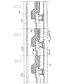
図1には、第1の電極101と、第2の電極102との間に、第1の発光ユニット100
B、第2の発光ユニット100G、第3の発光ユニット100Rが順に積層された発光素
子を示す。何れの発光ユニットが、どの様な発光色を呈するかについて特に限定はないが
、本形態では、第1の発光ユニットが青色の発光を呈し、第2の発光ユニットが緑色の発
光を呈し、第3の発光ユニットが赤色の発光を呈する場合について説明する。なお、積層
された発光ユニットとは、2以上の発光ユニットが積層された状態を指し、本実施の形態
では3つの発光ユニットが積層された状態で説明するが、本発明はこれに限定されるもの
ではない。
In FIG. 1, the first
B shows a light emitting element in which a second
図1に示す発光素子では、第1の電極101を反射性の高い材料で形成し、第2の電極1
02を透光性の高い材料で形成し、第2の電極102から光を取り出す。各発光ユニット
100R、100G、100Bは、それぞれ第1の層111R、111G、111B、第
2の層112R、112G、112B、第3の層113R、113G、113Bを有する
。
In the light-emitting element illustrated in FIG. 1, the
02 is formed using a highly light-transmitting material, and light is extracted from the
このような発光素子において、発光層を有する層として第2の層112(112B,11
2G,112R)を用いる場合、各発光素子の第2の層112と第1の電極101との距
離を、第1の層111(111B,111G,111R)の膜厚によって1/4波長の奇
数倍とすることを特徴とする。すなわち、発光層と、第1の電極101との距離を、その
間に設けられた層の厚みによって1/4波長の奇数倍とすることを特徴とする。そのため
、発光ユニットごとに第1の層111R、111G、111Bの膜厚が異なる。
In such a light-emitting element, the second layer 112 (112B, 11B) is provided as a layer having a light-emitting layer.
2G, 112R), the distance between the
発光ユニットを積層しているため、発光取り出し効率を高めるために各発光層と第1の電
極101との距離はそれぞれ異なる。そのため、各発光層と第1の電極101との間に設
けられた第1の層111の厚みをそれぞれ制御した発光素子を提供する。その結果、発光
取り出し効率が高い状態を提供する。
Since the light emitting units are stacked, the distance between each light emitting layer and the
このように発光ユニットを積層することにより、発光効率を高めることができるため、流
す電流量を低く維持することができ、発光素子の寿命を向上させることができる。
By stacking the light emitting units in this manner, the light emission efficiency can be increased, so that the amount of current that flows can be kept low and the life of the light emitting element can be improved.
なお本実施の形態では、すべての第1の層111R、111G、111Bの膜厚を制御し
た形態を示すが、本発明は積層された発光ユニットが有する第1の層111のいずれか一
つの膜厚を制御すればよい。いずれか一つの第1の層111を制御することによって、発
光取り出し効率が高い状態を提供でき、流す電流量を低く維持する効果を奏することがで
きるからである。
Note that this embodiment mode shows a mode in which the film thicknesses of all the
なお本発明において、積層された発光層は異色の発光を呈する層を有する必要はない。す
なわち本発明は、同色の発光を呈する層を積層してもよい。同色の発光を呈する層を積層
しても、発光効率が高い状態を提供でき、流す電流量を低く維持する効果を奏することが
できるからである。
In the present invention, the stacked light emitting layers do not need to have a layer that emits light of different colors. In other words, in the present invention, layers that emit light of the same color may be stacked. This is because even when layers exhibiting light emission of the same color are stacked, a state in which light emission efficiency is high can be provided, and an effect of maintaining a low amount of current to flow can be achieved.
また本発明では、第1の層111に導電性の高い材料を用い、当該第1の層111の膜厚
を制御するため、特許文献1等に記載される従来の素子と比較して、駆動電圧を低くする
ことができる。
In the present invention, a highly conductive material is used for the
第1の層111乃至第3の層113(113B,113G,113R)は、スパッタリン
グ法や蒸着法等を用いて形成することができる。
The
次に電極について説明する。第1の電極101は反射性を有する材料から形成し、第2の
電極102は透光性を有する材料で形成する。なお透光性を有するためには、非透光性を
有する材料を非常に薄く形成することによって、得ることもできる。
Next, the electrode will be described. The
第1の電極101の材料は、チタン(Ti)、アルミニウム(Al)、金(Au)、白金
(Pt)、ニッケル(Ni)、タングステン(W)、クロム(Cr)、モリブデン(Mo
)、鉄(Fe)、コバルト(Co)、銅(Cu)、若しくはパラジウム(Pd)等の金属
材料を用いることができ、上記金属材料の単層、又は積層を用いることができる。なお、
第1の電極101は、例えばスパッタ法や蒸着法等を用いて形成することができる。
The material of the
), Iron (Fe), cobalt (Co), copper (Cu), palladium (Pd), or the like, and a single layer or a stacked layer of the above metal materials can be used. In addition,
The
また、第2の電極102の材料は、インジウム錫酸化物(ITO)、酸化珪素を含むイン
ジウム錫酸化物、2〜20%の酸化亜鉛を含む酸化インジウム等の透光性材料を用いるこ
とができる。その他、金(Au)、白金(Pt)、ニッケル(Ni)、タングステン(W
)、クロム(Cr)、モリブデン(Mo)、鉄(Fe)、コバルト(Co)、銅(Cu)
、若しくはパラジウム(Pd)等の非透光性を有する金属材料であって、透光性を有する
程度に薄膜化して用いることができる。また第2の電極102は、上記金属材料の単層、
又は積層を用いることができる。積層構造を用いる場合、上記非透光性を有する金属材料
を薄膜化し、その上に透光性材料を積層する構成を用いることもできる。第2の電極10
2を薄く形成することにより、抵抗が高くなることを防止するため、補助配線を設けるこ
ともできる。
The material of the
), Chromium (Cr), molybdenum (Mo), iron (Fe), cobalt (Co), copper (Cu)
Alternatively, it is a non-light-transmitting metal material such as palladium (Pd), and can be used after being thinned to such an extent that it has light-transmitting properties. The
Alternatively, a stack can be used. In the case of using a stacked structure, a structure in which the above-described non-light-transmitting metal material is thinned and a light-transmitting material is stacked thereover can also be used.
In order to prevent the resistance from becoming high by forming 2 thin, an auxiliary wiring can also be provided.
なお第1の電極101又は第2の電極102は、発光素子に印加する電圧によって、それ
ぞれ陽極又は陰極となり得る。陽極となる場合は、仕事関数の大きい(仕事関数4.0e
V以上)材料とし、陰極となる場合は、仕事関数の小さい(仕事関数3.8eV以下)材
料とすることが好ましい。
Note that the
(V or higher) material, and when it becomes a cathode, it is preferable to use a material having a low work function (work function of 3.8 eV or lower).
第1の電極101、又は第2の電極102は、スパッタリング法や蒸着法等を用いて形成
することができる。なお蒸着法を用いる場合、第1の電極101、第1の層111乃至第
3の層113、第2の電極102を、大気解放することなく連続して形成することが可能
となる。このように大気解放することなく連続して発光素子を形成することにより、界面
等への不純物混入を低減することができる。
The
このような本発明の発光素子は、各発光層と第1の電極101との間に設けられた第1の
層111の厚みを制御し、発光取り出し効率が高い状態を得ることができる。さらに本発
明は発光ユニットを積層することにより、同じ電流密度における発光効率を高めることが
できるため、電流密度を低く維持することができ、発光素子の寿命を向上させることがで
きる。
In such a light-emitting element of the present invention, the thickness of the
以上のように、積層された発光ユニットを有する発光装置は、鮮明な、画質の優れた映像
を表示でき、低消費電力を図ることができる。
As described above, a light-emitting device including stacked light-emitting units can display a clear image with excellent image quality, and can achieve low power consumption.
(実施の形態2)
本実施の形態では、上記実施の形態とは異なる発光素子の構造について説明する。
(Embodiment 2)
In this embodiment, a structure of a light-emitting element which is different from that in the above embodiment will be described.
本発明は、基板上に形成されたすべての発光素子に、発光層が積層された発光素子を適用
する必要はない。少なくとも一つの発光素子中に発光層を積層し、発光層と第1の電極1
01との距離を第1の層111により1/4波長の奇数倍とすることで、発光取り出し効
率が高い状態を得、同じ電流密度における発光効率を高めることができ、電流密度を低く
維持することができるからである。電流密度を低く維持する結果、発光素子の寿命を向上
させることができる。そこで本実施の形態では、少なくとも一つの発光色を呈する発光素
子を、発光層が積層された発光素子とする場合を説明する。
In the present invention, it is not necessary to apply a light emitting element in which a light emitting layer is laminated to all the light emitting elements formed on a substrate. A light emitting layer is stacked in at least one light emitting element, and the light emitting layer and the
By setting the distance to 01 to an odd multiple of a quarter wavelength by the
図2には、同一基板上に形成された第1の発光ユニット100B、第2の発光ユニット1
00G、第3の発光ユニット100Rが設けられた状態を示す。何れの発光素子が、どの
様な発光色を呈するかについて特に限定はないが、本形態では、第1の発光素子が青色の
発光を呈し、第2の発光素子が緑色の発光を呈し、第3の発光素子が赤色の発光を呈する
場合について説明する。
FIG. 2 shows the first
00G shows a state where the third
青色の発光を呈する発光素子は2つの発光ユニット100B(1)及び100B(2)が
積層された発光素子とする。便宜上このように積層された発光素子を積層型発光素子と呼
ぶ。また赤色及び緑色の発光を呈する発光ユニット100R、100Gはそれぞれ発光層
が単層からなる発光素子とし、便宜上単層型発光素子と呼ぶ。
A light emitting element that emits blue light is a light emitting element in which two light emitting
第1の電極101及び第2の電極102の構成は、上記実施の形態1と同様であるため説
明を省略する。
The configurations of the
このような積層型発光素子において、発光層と第1の電極101との距離を第1の層11
1(111B(1),111B(2))により1/4波長の奇数倍とする。その結果、発
光取り出し効率が向上し、同じ発光輝度を選るのに必要な電流密度を低く維持することが
できる。電流密度を低く維持する結果、発光素子の寿命を向上させることができる。各発
光ユニットには第2の層112(112(1),112B(2))、第3の層113(1
13B(1),113B(2))も含まれる。
In such a stacked light emitting element, the distance between the light emitting layer and the
1 (111B (1), 111B (2)) is an odd multiple of a quarter wavelength. As a result, the light emission extraction efficiency is improved, and the current density required to select the same light emission luminance can be kept low. As a result of keeping the current density low, the lifetime of the light emitting element can be improved. Each light emitting unit includes a second layer 112 (112 (1), 112B (2)) and a third layer 113 (1
13B (1), 113B (2)) are also included.
このように積層型発光素子は、発光効率を高めることができるため、電流密度を低く維持
することができ、寿命を向上させることができる。そのため、劣化の生じやすい発光素子
に対して、選択的に積層型発光素子を適用すると望ましい。
As described above, the stacked light-emitting element can increase the light emission efficiency, so that the current density can be kept low and the life can be improved. Therefore, it is desirable to selectively apply a stacked light emitting element to a light emitting element that easily deteriorates.
なお単層型発光素子においても、第1の層111(111G,111R)により、発光層
と第1の電極101との距離を1/4波長の奇数倍とすることができる。その結果、発光
取り出し効率を高めることができる。各発光ユニットには第2の層112(112G,1
12R)、第3の層113(113G,113R)も含まれる。
Note that also in the single-layer light-emitting element, the distance between the light-emitting layer and the
12R), the third layer 113 (113G, 113R) is also included.
また積層型発光素子及び単層型発光素子において、第1の層111に導電性の高い材料を
用い、当該第1の層111の膜厚を制御するため、特許文献1等に記載される従来の素子
と比較して、駆動電圧を低くすることができる。
In a stacked light-emitting element and a single-layer light-emitting element, a material having high conductivity is used for the
以上のように、少なくとも一つの発光色を呈する発光素子を積層型発光素子とする発光装
置は、鮮明な、画質の優れた映像を表示でき、低消費電力を図ることができる。
As described above, a light-emitting device using a light-emitting element exhibiting at least one emission color as a stacked light-emitting element can display a clear image with excellent image quality and can achieve low power consumption.
(実施の形態3)
本実施の形態では、上記実施の形態とは異なる発光色を呈する発光素子に積層型発光素子
を適用する場合について説明する。
(Embodiment 3)
In this embodiment, the case where a stacked light-emitting element is applied to a light-emitting element that emits light different from that in the above embodiment is described.
本発明では、第1の発光ユニット100B以外の発光素子を積層型発光素子としてもよく
、例えば緑色の発光のように人間の眼に対する感度の高い発光色を呈する発光ユニット1
00Gを単層とした単層型発光素子を用い、赤色あるいは青色の発光を呈する発光ユニッ
ト100R、100Bが積層された積層型発光素子としてもよい。さらに全発光素子にお
いて積層型発光素子とし、緑色を呈する発光ユニット100Gの積層数を、赤色あるいは
青色の発光を呈する発光ユニット100R、100Gの積層数よりも少なくする、つまり
一対の電極間に含まれる発光層の数を少なくなるように構成してもよい。
In the present invention, a light-emitting element other than the first light-emitting
A single-layer light-emitting element having a single layer of 00G may be used, and a stacked light-emitting element in which light-emitting
その他の構成は、上記実施の形態と同様であるため説明を省略する。 Since other configurations are the same as those in the above embodiment, the description thereof is omitted.
このような積層型発光素子において、発光層と第1の電極101との距離を第1の層11
1により1/4波長の奇数倍とする。その結果、発光取り出し効率が向上し、同じ輝度を
得るために必要な電流密度を低く維持することができる。電流密度を低く維持する結果、
発光素子の寿命を向上させることができる。
In such a stacked light emitting element, the distance between the light emitting layer and the
1 is an odd multiple of a quarter wavelength. As a result, the emission extraction efficiency is improved, and the current density necessary to obtain the same luminance can be kept low. As a result of keeping the current density low,
The lifetime of the light emitting element can be improved.
なお単層型発光素子においても、第1の層111により、発光層と第1の電極101との
距離を1/4波長の奇数倍とすることができる。その結果、発光取り出し効率を高めるこ
とができる。
Note that also in a single-layer light-emitting element, the distance between the light-emitting layer and the
このように、人間の眼に対する感度の低い発光色を呈する発光素子と、人間の眼に対する
感度の高い発光色を呈する発光素子とで一対の電極間に設ける発光層の数を異ならせるこ
とにより効率的に各色の輝度の調和をとることができる。
Thus, the efficiency is improved by making the number of light emitting layers provided between a pair of electrodes different between a light emitting element exhibiting a light emitting color with low sensitivity to human eyes and a light emitting element exhibiting a light emitting color with high sensitivity to human eyes. Therefore, the luminance of each color can be harmonized.
また積層型発光素子及び単層型発光素子において、第1の層111に導電性の高い材料を
用い、当該第1の層111の膜厚を制御するため、特許文献1等に記載される従来の素子
と比較して、駆動電圧を低くすることができる。
In a stacked light-emitting element and a single-layer light-emitting element, a material having high conductivity is used for the
以上のように、少なくとも一つの発光色を呈する発光素子を積層型発光素子とする発光装
置は、鮮明な、画質の優れた映像を表示でき、低消費電力を図ることができる。
As described above, a light-emitting device using a light-emitting element exhibiting at least one emission color as a stacked light-emitting element can display a clear image with excellent image quality and can achieve low power consumption.
(実施の形態4)
本実施の形態では、各発光ユニットの構造及び材料について説明する。
(Embodiment 4)
In this embodiment, the structure and material of each light-emitting unit will be described.
図3に示すように、単層型発光ユニットは、第1電極から順に、第1の層111、第2の
層112、第3の層113が積層されている。
As shown in FIG. 3, in the single-layer light emitting unit, a
このような発光ユニットを有する発光素子は、第2の電極の電位よりも第1の電極101
の電位が高くなるように電圧を印加すると、第1の層111から第2の層112へ正孔が
注入され、第3の層113から第2の層112へ電子が注入される。そして正孔と、電子
とが、第2の層112において再結合し、発光物質を励起状態にする。そして、励起状態
の発光物質は、基底状態に戻るときに発光する。
The light-emitting element having such a light-emitting unit has the
When a voltage is applied so as to increase the potential, holes are injected from the
これら第1の層111から第3の層113の材料について説明する。
The materials of the
第1の層111は、正孔を発生する層である。このような機能は、正孔輸送性物質と、そ
の物質に対して電子受容性を示す物質とを含む層とにすることより奏することができる。
なお正孔輸送性物質に対して電子受容性を示す物質は、正孔輸送性物質に対して、モル比
が0.5〜2(=正孔輸送性物質に対して電子受容性を示す物質/正孔輸送性物質)と成
るように含まれていると好ましい。
The
In addition, the substance which shows an electron-accepting property with respect to a hole transportable substance is 0.5-2 (molar ratio with respect to a hole-transportable substance) (= substance which shows an electron accepting property with respect to a hole-transportable substance) / Hole transporting material) is preferably included.
正孔輸送性物質とは、電子よりも正孔の輸送性が高い物質であり、例えば、4,4’−ビ
ス[N−(1−ナフチル)−N−フェニルアミノ]ビフェニル(略称:α−NPD)、4
,4’−ビス[N−(3−メチルフェニル)−N−フェニルアミノ]ビフェニル(略称:
TPD)、4,4’,4’’−トリス(N,N−ジフェニルアミノ)トリフェニルアミン
(略称:TDATA)、4,4’,4’’−トリス[N−(3−メチルフェニル)−N−
フェニルアミノ]トリフェニルアミン(略称:MTDATA)、4,4’−ビス[N−{
4−(N,N−ジ−m−トリルアミノ)フェニル}−N−フェニルアミノ]ビフェニル(
略称:DNTPD)等の芳香族アミン化合物や、フタロシアニン(略称:H2Pc)、銅
フタロシアニン(略称:CuPc)、バナジルフタロシアニン(略称:VOPc)等のフ
タロシアニン化合物等の有機化合物を用いることができる。なお、正孔輸送性物質は、こ
れらに限定されるものではない。
The hole-transporting substance is a substance that has a higher hole-transporting property than electrons. For example, 4,4′-bis [N- (1-naphthyl) -N-phenylamino] biphenyl (abbreviation: α- NPD), 4
, 4′-bis [N- (3-methylphenyl) -N-phenylamino] biphenyl (abbreviation:
TPD), 4,4 ′, 4 ″ -tris (N, N-diphenylamino) triphenylamine (abbreviation: TDATA), 4,4 ′, 4 ″ -tris [N- (3-methylphenyl)- N-
Phenylamino] triphenylamine (abbreviation: MTDATA), 4,4′-bis [N- {
4- (N, N-di-m-tolylamino) phenyl} -N-phenylamino] biphenyl (
An aromatic amine compound such as abbreviation: DNTPD, or an organic compound such as a phthalocyanine compound such as phthalocyanine (abbreviation: H 2 Pc), copper phthalocyanine (abbreviation: CuPc), or vanadyl phthalocyanine (abbreviation: VOPc) can be used. Note that the hole transporting substance is not limited to these.
また、正孔輸送性物質に対して電子受容性を示す物質は、例えば周期表第4族乃至第12
族のいずれかから選ばれた金属の酸化物(金属酸化物)を用いることができる。中でも、
周期表第4族乃至第8族のいずれかの金属酸化物は電子受容性の高いものが多く、特にバ
ナジウム酸化物、モリブデン酸化物、ニオブ酸化物、レニウム酸化物、タングステン酸化
物、ルテニウム酸化物、チタン酸化物、クロム酸化物、ジルコニウム酸化物、ハフニウム
酸化物、タンタル酸化物が好適である。酸化物以外であっても、上記金属の窒化物、酸化
窒化物を用いてもよい。なお正孔輸送性物質に対して電子受容性を示す物質は、これらに
限定されるものではなく、三塩化鉄(FeCl3)、三塩化アルミ(AlCl3)、7,
7,8,8−テトラシアノ−2,3,5,6−テトラフルオロ−キノジメタン(略称:F
4TCNQ)を用いてもよい。
In addition, examples of the substance that exhibits an electron accepting property with respect to the hole transporting substance include
A metal oxide (metal oxide) selected from any of the above groups can be used. Above all,
Many metal oxides of
7,8,8-tetracyano-2,3,5,6-tetrafluoro-quinodimethane (abbreviation: F
4 TCNQ) may be used.
このように第1の層111は、有機化合物からなる正孔輸送性物質と、上記金属酸化物か
らなる正孔輸送性物質に対して電子受容性を示す物質とが混在した層から形成する。なお
、混在した層とは、有機化合物と無機化合物とが混成された層、各々薄く積層された層が
含まれる。
As described above, the
このような有機化合物と、無機化合物とが混在した層を用いることによって、当該有機化
合物の結晶化を抑制することができ、抵抗の増加を伴わずに第1の層111を厚く形成す
ることが可能となる。さらに、有機化合物と、上記金属酸化物からなる正孔輸送性物質に
対して電子受容性を示す物質とが混在した層は導電性が高くなるため、抵抗の上昇を伴わ
ずに厚膜化を図ることができる。そのため、第1の電極101上にゴミや汚れ等に起因す
る凹凸がある場合であっても、第1の層111の厚膜化によりこの凹凸の影響をほとんど
受けない。従って、凹凸に起因する第1の電極101と、第2の電極102とのショート
等の不良を防止することができる。また第1の層111を厚膜化することにより、第1の
電極101と、第2の層112とを離すことができるので、金属に起因して発光が消光す
ることを防ぐこともできる。
By using a layer in which such an organic compound and an inorganic compound are mixed, crystallization of the organic compound can be suppressed, and the
なお第1の層111に、その他の有機化合物を含んでいてもよい。その他の有機化合物に
は、ルブレン等が挙げられる。ルブレンを加えることにより、信頼性を向上させることが
できる。
Note that the
このような第1の層111は、蒸着法により形成することができる。第1の層111とし
て、複数の化合物が混在した層を形成する場合には共蒸着法を用いるとよい。共蒸着法は
、抵抗加熱蒸着同士による共蒸着法、電子ビーム蒸着同士による共蒸着法、抵抗加熱蒸着
と電子ビーム蒸着による共蒸着法がある。また、その他抵抗加熱蒸着とスパッタリング法
による成膜、電子ビーム蒸着とスパッタリングによる成膜など、同種、異種方法を組み合
わせて、第1の層111を形成してもよい。また、上記例は2種の材料を含む層を示して
いるが、3種以上の材料を含む場合も同様に、同種、異種方法を組み合わせて形成するこ
とができる。
Such a
次に、発光層を含む層である第2の層112について説明する。発光層を含む層とは、発
光層のみからなる単層であっても、発光層を含む多層でも構わない。具体的な多層の構造
は、発光層の他、電子輸送層、及び正孔輸送層のいずれから選ばれた層を含む。図3では
、第2の層112が正孔輸送層122、発光層123、電子輸送層124を含む多層の場
合を示す。
Next, the
正孔輸送層122は、公知な材料から形成することができる。典型的な例としては、芳香
族アミン系化合物であり、例えば、4,4’−ビス[N−(1−ナフチル)−N−フェニ
ル−アミノ]−ビフェニル(以下、α−NPDと示す)や、4,4’,4’’−トリス(
N,N−ジフェニル−アミノ)−トリフェニルアミン(以下、TDATAと示す)、4,
4’,4’’−トリス[N−(3−メチルフェニル)−N−フェニル−アミノ]−トリフ
ェニルアミン(以下、MTDATAと示す)などのスターバースト型芳香族アミン化合物
が挙げられる。
The
N, N-diphenyl-amino) -triphenylamine (hereinafter referred to as TDATA), 4,
Starburst type aromatic amine compounds such as 4 ′, 4 ″ -tris [N- (3-methylphenyl) -N-phenyl-amino] -triphenylamine (hereinafter referred to as MTDATA) can be mentioned.
発光層123は、発光物質が、発光物質の有するエネルギーギャップよりも大きいエネル
ギーギャップを有する物質からなる層中に、分散して含まれた層であることが好ましい。
なお、エネルギーギャップとはLUMO準位とHOMO準位との間のエネルギーギャップ
をいう。また発光物質は、発光効率が良好で、所望の発光波長の発光をし得る物質を用い
ればよい。
The light-emitting
Note that the energy gap is an energy gap between the LUMO level and the HOMO level. As the light-emitting substance, a substance that has favorable emission efficiency and can emit light with a desired emission wavelength may be used.
発光物質を分散状態にするために用いる物質は、例えば、9,10−ジ(2−ナフチル)
−2−tert−ブチルアントラセン(略称:t−BuDNA)等のアントラセン誘導体
、または4,4’−ビス(N−カルバゾリル)ビフェニル(略称:CBP)等のカルバゾ
ール誘導体の他、ビス[2−(2−ヒドロキシフェニル)ピリジナト]亜鉛(略称:Zn
pp2)、ビス[2−(2−ヒドロキシフェニル)ベンゾオキサゾラト]亜鉛(略称:Z
nBOX)等の金属錯体等を用いることができる。但し、発光物質を分散状態にするため
に用いる物質はこれらの材料に限定されない。発光物質を分散状態として有する発光層1
23は、発光物質からの発光が、濃度に起因して消光してしまうことを防ぐことができる
。
The substance used to make the luminescent substance dispersed is, for example, 9,10-di (2-naphthyl)
In addition to anthracene derivatives such as 2-tert-butylanthracene (abbreviation: t-BuDNA) or carbazole derivatives such as 4,4′-bis (N-carbazolyl) biphenyl (abbreviation: CBP), bis [2- (2 -Hydroxyphenyl) pyridinato] zinc (abbreviation: Zn
pp 2 ), bis [2- (2-hydroxyphenyl) benzoxazolate] zinc (abbreviation: Z
A metal complex such as nBOX) can be used. However, substances used for bringing the light-emitting substance into a dispersed state are not limited to these materials. Light-emitting
No. 23 can prevent the light emitted from the luminescent material from being quenched due to the concentration.
次に発光層123の発光物質を示す。赤色の発光を得たいときには、4−ジシアノメチレ
ン−2−イソプロピル−6−[2−(1,1,7,7−テトラメチルジュロリジン−9−
イル)エテニル]−4H−ピラン(略称:DCJTI)、4−ジシアノメチレン−2−メ
チル−6−[2−(1,1,7,7−テトラメチルジュロリジン−9−イル)エテニル]
−4H−ピラン(略称:DCJT)、4−ジシアノメチレン−2−tert−ブチル−6
−[2−(1,1,7,7−テトラメチルジュロリジン−9−イル)エテニル]−4H−
ピラン(略称:DCJTB)やペリフランテン、2,5−ジシアノ−1,4−ビス[2−
(10−メトキシ−1,1,7,7−テトラメチルジュロリジン−9−イル)エテニル]
ベンゼン等を用いることができる。但しこれらの材料に限定されず、600nmから68
0nmに発光スペクトルのピークを有する発光を呈する物質を用いることができる。
Next, a light-emitting substance of the light-emitting
Yl) ethenyl] -4H-pyran (abbreviation: DCJTI), 4-dicyanomethylene-2-methyl-6- [2- (1,1,7,7-tetramethyljulolidin-9-yl) ethenyl]
-4H-pyran (abbreviation: DCJT), 4-dicyanomethylene-2-tert-butyl-6
-[2- (1,1,7,7-tetramethyljulolidin-9-yl) ethenyl] -4H-
Pyran (abbreviation: DCJTB), periflanthene, 2,5-dicyano-1,4-bis [2-
(10-methoxy-1,1,7,7-tetramethyljulolidin-9-yl) ethenyl]
Benzene or the like can be used. However, it is not limited to these materials, and 600 nm to 68
A substance exhibiting light emission having an emission spectrum peak at 0 nm can be used.
緑色の発光を得たいときは、N,N’−ジメチルキナクリドン(略称:DMQd)、クマ
リン6やクマリン545T、トリス(8−キノリノラト)アルミニウム(略称:Alq3
)等を用いることができる。但しこれらの材料に限定されず、500nmから550nm
に発光スペクトルのピークを有する発光を呈する物質を用いることができる。
When green light emission is desired, N, N′-dimethylquinacridone (abbreviation: DMQd),
) Etc. can be used. However, it is not limited to these materials, 500 nm to 550 nm
A substance exhibiting light emission having an emission spectrum peak can be used.
青色の発光を得たいときは、9,10−ジ(2−ナフチル)−2−tert−ブチルアン
トラセン(略称:t−BuDNA)、9,9’−ビアントリル、9,10−ジフェニルア
ントラセン(略称:DPA)、9,10−ビス(2−ナフチル)アントラセン(略称:D
NA)、ビス(2−メチル−8−キノリノラト)−4−フェニルフェノラト−ガリウム(
略称:BGaq)、ビス(2−メチル−8−キノリノラト)−4−フェニルフェノラト−
アルミニウム(略称:BAlq)等を用いることができる。但しこれらの材料に限定され
ず、420nmから500nmに発光スペクトルのピークを有する発光を呈する物質を用
いることができる。
To obtain blue light emission, 9,10-di (2-naphthyl) -2-tert-butylanthracene (abbreviation: t-BuDNA), 9,9′-bianthryl, 9,10-diphenylanthracene (abbreviation: DPA), 9,10-bis (2-naphthyl) anthracene (abbreviation: D)
NA), bis (2-methyl-8-quinolinolato) -4-phenylphenolato-gallium (
Abbreviations: BGaq), bis (2-methyl-8-quinolinolato) -4-phenylphenolato
Aluminum (abbreviation: BAlq) or the like can be used. However, the present invention is not limited to these materials, and a substance exhibiting light emission having an emission spectrum peak from 420 nm to 500 nm can be used.
このような発光物質を選択することにより、フルカラー表示の発光装置を作製することが
できる。
By selecting such a light emitting substance, a light emitting device for full color display can be manufactured.
また白色の発光を得たいときは、例えば、第1の電極101側から順に、TPD(芳香族
ジアミン)、3−(4−tert−ブチルフェニル)−4−フェニル−5−(4−ビフェ
ニリル)−1,2,4−トリアゾール(略称:TAZ)、トリス(8−キノリノラト)ア
ルミニウム(略称:Alq3)、赤色発光色素であるナイルレッドをドープしたAlq3
、そしてAlq3を蒸着法等により積層して形成する。
When obtaining white light emission, for example, in order from the
Then, Alq 3 is formed by laminating by vapor deposition or the like.
その他にも、第1の電極101側から順に、α−NPD、ペリレンをドープしたα−NP
D、DCM1をドープしたビス(2−メチル−8−キノリノラト)−4−フェニルフェノ
ラト−アルミニウム(略称:BAlq)、Alq3を蒸着法等により積層してもよい。
In addition, α-NPD and α-NP doped with perylene in order from the
D, Bis (2-methyl-8-quinolinolato) -4-phenylphenolato-aluminum (abbreviation: BAlq), Alq 3 doped with DCM1 may be stacked by a vapor deposition method or the like.
また、30wt%の2−(4−ビフェニリル)−5−(4−tert−ブチルフェニル)
−1,3,4−オキサジアゾール(略称:PBD)を電子輸送剤としてポリ(N−ビニル
カルバゾール)(略称:PVK)に分散し、4種類の色素(TPB、クマリン6、DCM
1、ナイルレッド)を適当量分散することで白色の発光を得ることができる。
Moreover, 30 wt% 2- (4-biphenylyl) -5- (4-tert-butylphenyl)
-1,3,4-oxadiazole (abbreviation: PBD) is dispersed in poly (N-vinylcarbazole) (abbreviation: PVK) as an electron transport agent, and four types of dyes (TPB,
1, Nile red) can be dispersed in an appropriate amount to obtain white light emission.
なお上記の赤色、青色、緑色、白色のいずれかの単色表示の発光装置を形成する場合であ
っても、カラーフィルターによって所望の発光を呈することができ、フルカラー表示を行
うこともできる。
Even in the case of forming the above-described light emitting device for single color display of red, blue, green, or white, the color filter can provide desired light emission, and full color display can also be performed.
このような発光層123として、有機化合物に金属酸化物を混在させた層を用いてもよい
。有機化合物と、金属酸化物とが混在した層を用いることによって、抵抗の増加を伴わず
に第2の層112を厚く形成することが可能となる。
As such a
次いで電子輸送層124について説明する。電子輸送層124とは、第2の電極102か
ら注入された電子を発光層123へ輸送する機能を有する層である。このように、電子輸
送層124を設け、第2の電極102と発光層123とをより離すことによって、発光が
金属に起因して消光することを防ぐことができる。
Next, the
電子輸送層124は、正孔の移動度よりも電子の移動度が高い物質を用いて形成すること
が好ましい。また、電子輸送層124は、10−6cm2/Vs以上の電子移動度を有す
る物質を用いて形成することがより好ましい。また、電子輸送層124は、以上に述べた
物質からなる層を二以上組み合わせて形成した多層構造の層であってもよい。具体的な電
子輸送層の材料は、トリス(8−キノリノラト)アルミニウム(略称:Alq3)、トリ
ス(5−メチル−8−キノリノラト)アルミニウム(略称:Almq3)、ビス(10−
ヒドロキシベンゾ[h]−キノリナト)ベリリウム(略称:BeBq2)、先に述べたB
Alqなど、キノリン骨格またはベンゾキノリン骨格を有する金属錯体が好適である。
また、ビス[2−(2−ヒドロキシフェニル)−ベンゾオキサゾラト]亜鉛(略称:Zn
(BOX)2)、ビス[2−(2−ヒドロキシフェニル)−ベンゾチアゾラト]亜鉛(略
称:Zn(BTZ)2)などのオキサゾール系、チアゾール系配位子を有する金属錯体も
ある。さらに、金属錯体以外にも、2−(4−ビフェニリル)−5−(4−tert−ブ
チルフェニル)−1,3,4−オキサジアゾール(略称:PBD)や、1,3−ビス[5
−(p−tert−ブチルフェニル)−1,3,4−オキサジアゾール−2−イル]ベン
ゼン(略称:OXD−7)、3−(4−tert−ブチルフェニル)−4−フェニル−5
−(4−ビフェニリル)−1,2,4−トリアゾール(略称:TAZ)、3−(4−te
rt−ブチルフェニル)−4−(4−エチルフェニル)−5−(4−ビフェニリル)−1
,2,4−トリアゾール(略称:p−EtTAZ)、バソフェナントロリン(略称:BP
hen)、バソキュプロイン(略称:BCP)なども用いることができる。
The
Hydroxybenzo [h] -quinolinato) beryllium (abbreviation: BeBq 2 ), B mentioned above
A metal complex having a quinoline skeleton or a benzoquinoline skeleton such as Alq is preferable.
In addition, bis [2- (2-hydroxyphenyl) -benzoxazolate] zinc (abbreviation: Zn
There are metal complexes having an oxazole-based or thiazole-based ligand such as (BOX) 2 ), bis [2- (2-hydroxyphenyl) -benzothiazolate] zinc (abbreviation: Zn (BTZ) 2 ). In addition to metal complexes, 2- (4-biphenylyl) -5- (4-tert-butylphenyl) -1,3,4-oxadiazole (abbreviation: PBD), 1,3-bis [5
-(P-tert-butylphenyl) -1,3,4-oxadiazol-2-yl] benzene (abbreviation: OXD-7), 3- (4-tert-butylphenyl) -4-phenyl-5
-(4-biphenylyl) -1,2,4-triazole (abbreviation: TAZ), 3- (4-te
rt-butylphenyl) -4- (4-ethylphenyl) -5- (4-biphenylyl) -1
2,4-triazole (abbreviation: p-EtTAZ), bathophenanthroline (abbreviation: BP)
hen), bathocuproine (abbreviation: BCP), and the like can also be used.
このような第2の層112は、単層構造であっても、積層構造であっても、蒸着法により
作製することができる。なお第2の層112を構成する層のうち、混在した層を形成する
場合には共蒸着法を用いることができる。共蒸着法は、抵抗加熱蒸着同士による共蒸着法
、電子ビーム蒸着同士による共蒸着法、抵抗加熱蒸着と電子ビーム蒸着による共蒸着法が
ある。また、その他抵抗加熱蒸着とスパッタリング法による成膜、電子ビーム蒸着とスパ
ッタリングによる成膜など、同種、異種方法を組み合わせて第2の層112を形成するこ
とができる。また、上記例は2種の材料を含む層を示しているが、3種以上の材料を含む
場合も同様に、同種、異種方法を組み合わせて形成することができることは、上述のとお
りである。
Such a
次いで電子を発生する層である第3の層113について説明する。このような第3の層1
13は、例えば、電子輸送性物質と、その物質に対して電子供与性を示す物質とを含む層
が挙げられる。
Next, the
Examples of the
なお電子輸送性物質とは、正孔よりも電子の輸送性が高い物質であり、例えば、トリス(
8−キノリノラト)アルミニウム(略称:Alq3)、トリス(4−メチル−8−キノリ
ノラト)アルミニウム(略称:Almq3)、ビス(10−ヒドロキシベンゾ[h]−キ
ノリナト)ベリリウム(略称:BeBq2)、ビス(2−メチル−8−キノリノラト)−
4−フェニルフェノラト−アルミニウム(略称:BAlq)、ビス[2−(2−ヒドロキ
シフェニル)ベンゾオキサゾラト]亜鉛(略称:Zn(BOX)2)、ビス[2−(2−
ヒドロキシフェニル)ベンゾチアゾラト]亜鉛(略称:Zn(BTZ)2)等の金属錯体
の他、2−(4−ビフェニリル)−5−(4−tert−ブチルフェニル)−1,3,4
−オキサジアゾール(略称:PBD)、1,3−ビス[5−(p−tert−ブチルフェ
ニル)−1,3,4−オキサジアゾール−2−イル]ベンゼン(略称:OXD−7)、3
−(4−tert−ブチルフェニル)−4−フェニル−5−(4−ビフェニリル)−1,
2,4−トリアゾール(略称:TAZ)、3−(4−tert−ブチルフェニル)−4−
(4−エチルフェニル)−5−(4−ビフェニリル)−1,2,4−トリアゾール(略称
:p−EtTAZ)、バソフェナントロリン(略称:BPhen)、バソキュプロイン(
略称:BCP)、4,4’ −ビス(5−メチル−ベンゾオキサゾール−2−イル)スチ
ルベン(略称:BzOs)等を用いることができる。また第3の層113は、n型の半導
体を用いて形成することができる。但し、電子輸送性物質はこれらに限定されない。
Note that the electron transporting substance is a substance having a higher electron transporting property than holes.
8-quinolinolato) aluminum (abbreviation: Alq 3 ), tris (4-methyl-8-quinolinolato) aluminum (abbreviation: Almq 3 ), bis (10-hydroxybenzo [h] -quinolinato) beryllium (abbreviation: BeBq 2 ), Bis (2-methyl-8-quinolinolato)-
4-phenylphenolato-aluminum (abbreviation: BAlq), bis [2- (2-hydroxyphenyl) benzoxazolate] zinc (abbreviation: Zn (BOX) 2 ), bis [2- (2-
In addition to metal complexes such as (hydroxyphenyl) benzothiazolate] zinc (abbreviation: Zn (BTZ) 2 ), 2- (4-biphenylyl) -5- (4-tert-butylphenyl) -1,3,4
-Oxadiazole (abbreviation: PBD), 1,3-bis [5- (p-tert-butylphenyl) -1,3,4-oxadiazol-2-yl] benzene (abbreviation: OXD-7), 3
-(4-tert-butylphenyl) -4-phenyl-5- (4-biphenylyl) -1,
2,4-triazole (abbreviation: TAZ), 3- (4-tert-butylphenyl) -4-
(4-ethylphenyl) -5- (4-biphenylyl) -1,2,4-triazole (abbreviation: p-EtTAZ), bathophenanthroline (abbreviation: BPhen), bathocuproin (
Abbreviations: BCP), 4,4′-bis (5-methyl-benzoxazol-2-yl) stilbene (abbreviation: BzOs), and the like can be used. The
また、電子輸送性物質に対して電子供与性を示す物質は、アルカリ金属およびアルカリ土
類金属の中から選ばれた物質、具体的にはリチウム(Li)、カルシウム(Ca)、ナト
リウム(Na)、カリウム(K)、マグネシウム(Mg)等を用いることができる。
In addition, the substance that exhibits an electron donating property with respect to the electron transporting substance is a substance selected from alkali metals and alkaline earth metals, specifically lithium (Li), calcium (Ca), and sodium (Na). , Potassium (K), magnesium (Mg), or the like can be used.
また、アルカリ金属酸化物またはアルカリ土類金属酸化物、アルカリ金属窒化物、アルカ
リ土類金属窒化物等も電子輸送性物質に対して電子供与性を示すことができる。これらの
具体的な材料としては、リチウム酸化物(Li2O)、カルシウム酸化物(CaO)、ナ
トリウム酸化物(Na2O)、カリウム酸化物(K2O)、マグネシウム酸化物(MgO
)等である。同等の効果が期待される材料として、アルカリ金属の窒化物又はフッ化物、
アルカリ土類金属の窒化物又はフッ化物があり、具体的にはフッ化リチウム(LiF)、
フッ化セシウム(CsF)、フッ化カルシウム(CaF2)等が挙げられる。但し、電子
輸送物質に対して電子供与性を示す物質は、これらに限定されない。なお、電子輸送性物
質に対して電子供与性を示す物質は、電子輸送性物質に対して、モル比が0.5〜2(=
電子輸送性物質に対して電子供与性を示す物質/電子輸送性物質)と成るように含まれて
いることが好ましい。
Alkali metal oxides or alkaline earth metal oxides, alkali metal nitrides, alkaline earth metal nitrides, and the like can also exhibit an electron donating property with respect to an electron transporting substance. Specific examples of these materials include lithium oxide (Li 2 O), calcium oxide (CaO), sodium oxide (Na 2 O), potassium oxide (K 2 O), and magnesium oxide (MgO).
) Etc. As a material expected to have an equivalent effect, an alkali metal nitride or fluoride,
There are alkaline earth metal nitrides or fluorides, specifically lithium fluoride (LiF),
Examples include cesium fluoride (CsF) and calcium fluoride (CaF 2 ). However, the substance that exhibits an electron donating property with respect to the electron transporting substance is not limited thereto. Note that a substance that exhibits an electron donating property with respect to an electron transporting substance has a molar ratio of 0.5 to 2 (=
It is preferable that it is contained so as to be a substance exhibiting an electron donating property with respect to an electron transporting substance / an electron transporting substance).
また、第3の層113は、酸化亜鉛、硫化亜鉛、セレン化亜鉛、酸化スズ、酸化チタンの
ような物質からなる層であってもよい。
The
また第3の層113は、有機化合物からなる電子輸送性物質と、電子輸送性物質に対して
電子供与性を示す物質とが混在した層から形成すると、好ましい。このような有機化合物
と、無機化合物とが混在した層を用いることによって、第3の層113に用いる有機化合
物の結晶化を抑制することができ、抵抗の増加を伴わずに第3の層113を厚く形成する
ことが可能となるからである。さらに、有機化合物と、上記金属酸化物からなる電子輸送
性物質に対して電子供与性を示す物質とが混在した層は導電性が高くなるため、抵抗の増
加を伴わずに厚膜化を図ることができる。そのため、基板上にゴミや汚れ等に起因する凹
凸がある場合であっても、第3の層113の厚膜化により凹凸の影響をほとんど受けない
。従って、凹凸に起因する第1の電極101と、第2の電極102とのショート等の不良
を防止することができる。このように第3の層113を厚膜化することにより、第1の電
極101と、第2の層112とを離すことができるので、金属に起因して発光が消光する
ことを防ぐこともできる。
The
電子輸送性物質に対して電子供与性を示す物質は、アルカリ金属およびアルカリ土類金属
の中から選ばれた物質、具体的にはリチウム(Li)、カルシウム(Ca)、ナトリウム
(Na)、カリウム(K)、マグネシウム(Mg)等から選ばれた金属の酸化物が挙げら
れる。具体的な金属酸化物としては、上記アルカリ金属の酸化物またはアルカリ土類金属
の酸化物が挙げられる。具体的には、リチウム酸化物(Li2O)、カルシウム酸化物(
CaO)、ナトリウム酸化物(Na2O)、カリウム酸化物(K2O)、マグネシウム酸
化物(MgO)等である。同等の効果が期待される材料として、アルカリ金属の窒化物又
はフッ化物、アルカリ土類金属の窒化物又はフッ化物があり、具体的にはフッ化リチウム
(LiF)、フッ化セシウム(CsF)、フッ化カルシウム(CaF2)等が挙げられる
。また同等の効果を得ることができれば、当該金属の酸化窒化物を用いてもよい。
The substance that exhibits an electron donating property with respect to the electron transporting substance is a substance selected from alkali metals and alkaline earth metals, specifically lithium (Li), calcium (Ca), sodium (Na), potassium Examples thereof include oxides of metals selected from (K), magnesium (Mg), and the like. Specific examples of the metal oxide include the above alkali metal oxides and alkaline earth metal oxides. Specifically, lithium oxide (Li 2 O), calcium oxide (
CaO), sodium oxide (Na 2 O), potassium oxide (K 2 O), magnesium oxide (MgO), and the like. Materials that are expected to have the same effect include alkali metal nitrides or fluorides, alkaline earth metal nitrides or fluorides, specifically lithium fluoride (LiF), cesium fluoride (CsF), Examples thereof include calcium fluoride (CaF 2 ). Further, an oxynitride of the metal may be used as long as an equivalent effect can be obtained.
このような第3の層113は、蒸着法により作製することができる。第3の層113とし
て、混在した層を形成する場合には共蒸着法を用いることができる。共蒸着法は、抵抗加
熱蒸着同士による共蒸着法、電子ビーム蒸着同士による共蒸着法、抵抗加熱蒸着と電子ビ
ーム蒸着による共蒸着法がある。また、その他抵抗加熱蒸着とスパッタリング法による成
膜、電子ビーム蒸着とスパッタリングによる成膜など、同種、異種方法を組み合わせて第
3の層113を形成することができる。また、上記例は2種の材料を含む層を示している
が、3種以上の材料を含む場合も同様に、同種、異種方法を組み合わせて形成することが
できることは、上述のとおりである。
Such a
なお積層型の発光ユニットを有する発光素子では、発光層間に設けられた第3の層113
は、いずれか一方の発光層にのみ励起エネルギーが移動してしまうことを阻止する層とし
ても機能する。このような第3の層113は、その下方に形成される発光層のイオン化ポ
テンシャルよりも大きいイオン化ポテンシャルを有すると共に、その上方に形成される発
光層のLUMO準位よりも大きいLUMO準位を有する層であることが好ましい。
Note that in a light-emitting element having a stacked light-emitting unit, a
Also functions as a layer that prevents excitation energy from moving to only one of the light emitting layers. Such a
第3の層113の厚さは1nm〜30nmとなるように形成されていることが好ましい。
The thickness of the
なお積層型の発光ユニットを有する発光素子では、各第1の層111、各第3の層113
にバイポーラ性の物質を用いてもよい。バイポーラ性の物質とは、電子または正孔のいず
れか一方のキャリアの移動度と他方のキャリアの移動度とを比較したときに、一方のキャ
リアの移動度に対する他方のキャリアの移動度の比の値が100以下、好ましくは10以
下である物質をいう。バイポーラ性の物質の中でも特に、正孔及び電子の移動度が1×1
0−6cm2/Vs以上の物質を用いることが好ましい。バイポーラ性の物質として、例
えば、2,3−ビス(4−ジフェニルアミノフェニル)キノキサリン(略称:TPAQn
)、2,3−ビス{4−[N−(1−ナフチル)−N−フェニルアミノ]フェニル}−ジ
ベンゾ[f,h]キノキサリン(略称:NPADiBzQn)等が挙げられる。また同一
のバイポーラ性の物質を用いて、各第1の層111、各第3の層113を形成しても構わ
ない。
Note that in the light-emitting element having the stacked light-emitting unit, the
Bipolar substances may be used. A bipolar substance is the ratio of the mobility of one carrier to the mobility of the other carrier when the mobility of one of the electrons or holes is compared with the mobility of the other carrier. A substance whose value is 100 or less, preferably 10 or less. Especially among bipolar substances, the mobility of holes and electrons is 1 × 1
It is preferable to use a substance of 0 −6 cm 2 / Vs or higher. As a bipolar substance, for example, 2,3-bis (4-diphenylaminophenyl) quinoxaline (abbreviation: TPAQn)
), 2,3-bis {4- [N- (1-naphthyl) -N-phenylamino] phenyl} -dibenzo [f, h] quinoxaline (abbreviation: NPDiBzQn), and the like. Alternatively, each
なお、本発明は発光取り出し効率が高くなるように、各発光素子の第1の層111の膜厚
を1/4波長の奇数倍とすることを特徴としており、図3に示す発光ユニットを有する発
光素子構成に限定されるものではない。例えば図3では、第3の層113に接して形成さ
れた電子輸送層124設ける構成を示したが、電子輸送層124を有しない場合もある。
この場合、発光層123が第3の層113と接する構成となるため、当該発光層123に
は、発光物質を分散状態とするための物質を用いるとよい。同様に、正孔輸送層122を
有しない場合もあり得る。
Note that the present invention is characterized in that the film thickness of the
In this case, since the light-emitting
また、Alq3等のように分散状態としなくても発光することができる物質を発光層12
3に用いてもよい。Alq3等は、キャリアの輸送性の良い発光物質であるため、分散状
態とすることなくAlq3のみからなる層を発光層123として機能させることができる
。
Further, a material that can emit light without being dispersed, such as Alq 3 , is used as the
3 may be used. Since Alq 3 or the like is a light-emitting substance with good carrier transportability, a layer made of only Alq 3 can function as the light-emitting
このような第1の層111から第3の層113の作製は、蒸着法等の同一方法により形成
することができる。そのため、大気解放することなく連続して形成することができる。こ
のように大気解放することなく連続して第1の層111から第3の層113を形成するこ
とにより、界面等への不純物混入を低減することができる。
The
次に、図3とは異なる発光ユニットの構造を図4に示す。 Next, FIG. 4 shows a structure of a light emitting unit different from that in FIG.
図4に示すように、本実施の形態に示す発光ユニットは、第1電極101から順に、第1
の層111、第2の層112、第3の層113、第4の層128が積層されており、第4
の層128を設けたことを特徴とする。第4の層128は、第1の層111と同様の材料
から形成することができ、その他の構成は、上述したとおりのため、説明を省略する。
As shown in FIG. 4, the light-emitting unit described in this embodiment includes a
The
このように第4の層128を設けると、第2の電極102を形成するときの各層へのダメ
ージを低減することができる。
When the
そして積層された発光ユニットにおいて、発光取り出し効率が高くなるように、各発光ユ
ニットの第1の層111の膜厚を異ならせる。膜厚を異ならせる場合、第4の層128も
第1の層111と同様に、有機化合物と金属酸化物とが混在された層を用いるとよい。第
4の層128に混在された層を用いることにより、厚膜化しても駆動電圧が上昇せず好ま
しいためである。なお金属酸化物と同等の効果を得ることができれば、金属の窒化物であ
ってもよいし、酸化窒化物であってもよい。
Then, in the stacked light emitting units, the thickness of the
そして第4の層128を厚膜化することにより、第2の電極102を形成するときのダメ
ージの、さらなる低減を期待できる。
Further, by increasing the thickness of the
また本発明は積層された発光ユニットにおいて、第1の層111、第4の層128に有機
化合物と、金属酸化物とが混在した層を用い、該層の膜厚により発光取り出し効率を高め
、さらには低駆動電圧化を達成した発光装置を提供することができる。また該層を厚くす
ることにより、発光層123と第1の電極101、又は発光層123と第2の電極102
とを離すことができるため、発光の消光を防止できる。そして発光ユニットを厚く形成す
ることができるので、電極間の短絡を防止でき、量産性を高めることができる。
Further, the present invention uses a layer in which an organic compound and a metal oxide are mixed in the
And can be prevented from being quenched. And since a light emitting unit can be formed thickly, the short circuit between electrodes can be prevented and mass productivity can be improved.
以上のような層を有する積層型の発光ユニットを有する発光素子を備えた発光装置は、鮮
明な、画質の優れた映像を表示でき、低消費電力を図ることができる。
A light-emitting device including a light-emitting element including a stacked light-emitting unit having the above layers can display a clear image with excellent image quality, and can achieve low power consumption.
(実施の形態5)
本実施の形態では、図5を用いて発光素子への電流の供給を制御するトランジスタ(駆動
用トランジスタ)がp型の薄膜トランジスタ(TFT)611の場合における、発光素子
603から発せられる光を第2の電極102側から取り出す上面出射型であって、3つ分
の画素の断面図について説明する。本実施の形態では、各RGBの発光を呈する発光ユニ
ット100R、100G、100Bを積層しているため、それぞれの色が混在し、白色と
して視認することができる。そのため、対向基板610に形成された各色カラーフィルタ
ー612R、612G、612Bにより、フルカラー表示を行う形態を示す。
(Embodiment 5)
In this embodiment mode, the light emitted from the
他に白色を呈する積層された発光素子は、赤色の発光が呈される発光ユニットと、青緑色
の発光が呈される発光ユニットとを積層する構成がある。それぞれの色が混合することに
より、白色として視認することができる。このように、積層型発光素子が有する複数の発
光ユニットからの発光色はそれぞれ異なっていてもよく、各発光ユニットの発光層と電極
との光学的距離は決定される。
Another stacked light-emitting element that exhibits white has a configuration in which a light-emitting unit that emits red light and a light-emitting unit that emits blue-green light are stacked. By mixing each color, it can be visually recognized as white. As described above, the light emission colors from the plurality of light emitting units included in the multilayer light emitting element may be different from each other, and the optical distance between the light emitting layer and the electrode of each light emitting unit is determined.
図5に示すように、基板600上にp型のTFT611を形成し、第1の電極101と、
TFT611が電気的に接続されている。また第1の電極101上に、各RGBの発光を
呈する発光ユニットが積層され、第2の電極102が順に積層されている。なお発光素子
の構造は、上記実施の形態で示したように第1の層111から第3の層113を有し、ま
たさらに第4の層128からなる場合がある。
As shown in FIG. 5, a p-
The
TFT611は、厚さが10nm乃至200nmであって、島状に分離された半導体膜に
形成されたチャネル形成領域、不純物元素が添加されたソース領域、及びドレイン領域を
有している。半導体膜は、非晶質半導体膜、結晶性半導体膜、微結晶半導体膜のいずれを
用いてもよい。例えば、結晶性半導体膜の場合、非晶質半導体膜を形成し、加熱処理によ
り得られた結晶性半導体膜がある。なお加熱処理とは、加熱炉、レーザー照射、若しくは
レーザー光の代わりにランプから発する光の照射(以下、ランプアニールと表記する)、
又はそれらを組み合わせて用いた処理のことである。レーザー照射を用いる場合、連続発
振型のレーザー(CWレーザー)又はパルス発振型のレーザー(パルスレーザー)を用い
ることができ、さらにそれらを併せて用いてもよい。例えば連続発振の基本波のレーザー
光と、連続発振の高調波のレーザー光とを照射するようにしてもよいし、連続発振の基本
波のレーザー光と、パルス発振の高調波のレーザー光とを照射するようにしてもよい。複
数のレーザー光を照射することにより、エネルギーを補うことができる。
The
Or it is the process which used them in combination. When laser irradiation is used, a continuous wave laser (CW laser) or a pulsed laser (pulse laser) can be used, and these may be used in combination. For example, a continuous wave fundamental laser beam and a continuous wave harmonic laser beam may be irradiated, or a continuous wave fundamental laser beam and a pulsed harmonic laser beam may be irradiated. You may make it irradiate. Energy can be supplemented by irradiating a plurality of laser beams.
さらにレーザー照射では、レーザーの入射角を半導体膜に対してθ(0°<θ<90°)
となるようにしてもよい。その結果、レーザーの干渉を防止することができる。
Furthermore, in laser irradiation, the incident angle of the laser is θ (0 ° <θ <90 °) with respect to the semiconductor film.
You may make it become. As a result, laser interference can be prevented.
またパルス発振型のレーザーであって、半導体膜がレーザー光によって溶融してから固化
するまでに、次のパルスのレーザー光を照射できるような発振周波数でレーザー光を発振
させることで、走査方向に向かって連続的に成長した結晶粒を得ることができるレーザー
を用いてもよい。このようなレーザーは、パルス発振の周期が、半導体膜が溶融してから
完全に固化するまでの時間よりも短くなるように、周波数の下限を定めたパルスビームを
用いる。実際に用いることができるパルスビームの発振周波数は10MHz以上であって
、通常用いられている数十Hz〜数百Hzの周波数帯よりも著しく高い周波数帯を使用す
る。
In addition, it is a pulse oscillation type laser that oscillates laser light at an oscillation frequency that can irradiate the laser light of the next pulse after the semiconductor film is melted by the laser light and solidifies in the scanning direction. You may use the laser which can obtain the crystal grain which grew continuously toward. Such a laser uses a pulse beam in which the lower limit of the frequency is set so that the period of pulse oscillation is shorter than the time from when the semiconductor film is melted until it is completely solidified. The oscillation frequency of the pulse beam that can be actually used is 10 MHz or more, and a frequency band that is significantly higher than the frequency band of several tens to several hundreds Hz that is normally used is used.
その他の加熱処理による結晶化手段として、加熱炉を用いる場合、非晶質半導体膜を50
0〜550℃で2〜20時間かけて加熱する方法がある。このとき、徐々に高温となるよ
うに温度を500〜550℃の範囲で多段階に設定するとよい。最初の低温加熱工程によ
り、半導体膜の水素等が出てくるため、結晶化の際の膜荒れを低減し、さらにダングリン
グボンドの終端を行うことができる。さらに、結晶化を促進させる金属元素、例えばNi
を非晶質半導体膜上に形成すると、加熱温度を低減することができ好ましい。このような
金属元素を用いた結晶化であっても、600〜950℃に加熱しても構わない。
When a heating furnace is used as a crystallization means by other heat treatment, an amorphous semiconductor film is formed in 50%.
There is a method of heating at 0 to 550 ° C. for 2 to 20 hours. At this time, the temperature may be set in multiple stages in the range of 500 to 550 ° C. so that the temperature gradually increases. In the first low-temperature heating step, hydrogen or the like of the semiconductor film is produced, so that film roughness during crystallization can be reduced and dangling bonds can be terminated. In addition, metal elements that promote crystallization, such as Ni
Is preferably formed over the amorphous semiconductor film because the heating temperature can be reduced. Even crystallization using such a metal element may be heated to 600 to 950 ° C.
但し、金属元素を形成する場合、半導体素子の電気特性に悪影響を及ぼすことが懸念され
るので、該金属元素を低減又は除去するためのゲッタリング工程を施す必要が生じる。例
えば、非晶質半導体膜をゲッタリングシンクとして金属元素を捕獲するよう工程を行えば
よい。
However, when a metal element is formed, there is a concern that the electrical characteristics of the semiconductor element may be adversely affected. Therefore, it is necessary to perform a gettering step for reducing or removing the metal element. For example, a process may be performed so as to capture a metal element using an amorphous semiconductor film as a gettering sink.
さらにTFT611は、該半導体膜を覆うゲート絶縁膜、ゲート電極を有し、該ゲート電
極上には水素を含む絶縁膜が設けられていてもよい。該水素によって、結晶性半導体膜中
のダングリングボンドを終端することができる。
Further, the
TFT611のソース領域及びドレイン領域は、高濃度不純物領域のみを有するシングル
ドレイン構造とする。またTFT611は、半導体膜のソース領域及びドレイン領域は、
低濃度不純物領域、及び高濃度不純物領域を有するLDD(低濃度ドレイン)構造として
もよい。なお低濃度不純物領域がゲート電極と重なったGOLD構造としてもよい。
The source region and the drain region of the
An LDD (low concentration drain) structure having a low concentration impurity region and a high concentration impurity region may be employed. Note that a GOLD structure in which the low concentration impurity region overlaps with the gate electrode may be employed.
TFT611は層間絶縁膜607で覆われており、層間絶縁膜607上には開口部を有す
る絶縁膜608が形成されている。なお本実施の形態において、層間絶縁膜607及び絶
縁膜608を有する構成に限定されず、層間絶縁膜607のみが設けられた構成であって
もよい。層間絶縁膜607は、単層構造であっても、積層構造であってもよく、無機材料
、又は有機材料、若しくは無機材料と有機材料との積層構造から形成することができる。
有機材料を用いると、平坦性を高めることができる。有機材料としては、ポリイミド、ア
クリル、ポリアミド、ポリイミドアミド、レジスト又はベンゾシクロブテンを用いること
ができる。層間絶縁膜607は、シロキサン、ポリシラザンを用いることができる。シロ
キサンとは、シロキサン系材料を出発材料として形成されたSi−O−Si結合を含む絶
縁膜である。またポリシラザンとは、珪素(Si)と窒素(N)の結合を有するポリマー
材料を含む液体材料を出発原料として形成される絶縁膜である。本実施の形態では、層間
絶縁膜607を無機材料から形成した構成を示す。
The
When an organic material is used, flatness can be improved. As the organic material, polyimide, acrylic, polyamide, polyimide amide, resist, or benzocyclobutene can be used. For the
絶縁膜608の開口部において、第1の電極101が一部露出しており、該開口部におい
て第1の電極101、発光ユニット100B、100G、100R、第2の電極102が
順に積層された積層型発光素子を形成している。
The
各発光ユニット100R、100G、100Bにおいては、各発光層123からの発光取
り出し効率が高くなるように、それぞれの第1の層111の膜厚が1/4波長の奇数倍と
されている。そして第1の層111には、有機化合物と、金属酸化物とが混在する層を用
い、厚膜化による駆動電圧の上昇を防止する。
In each of the
また各発光素子は、発光層123を有する第2の層112の他に、正孔輸送性物質を有す
る第1の層111、電子輸送性物質を有する第3の層113等を有していることは上述の
通りである。
In addition to the
本実施の形態では、TFT611がpチャネル型のため、第1の電極101を陽極とし、
第1の電極101から正孔輸送性物質を有する第1の層111、発光層123を有する第
2の層112、電子輸送性物質を有する第3の層113の順に積層する。なおTFT61
1がn型の場合、第1の電極101を陰極とすると好ましく、第1の電極101から、電
子輸送性物質を有する第3の層113、発光層123を有する第2の層112、正孔輸送
性物質を有する第1の層111の順に積層する。
In this embodiment mode, since the
A
In the case where 1 is an n-type, the
本実施の形態では、上面出射型であるため、第1の電極101は反射性(つまり非透光性
)を有し、第2の電極102は透光性を有する材料から形成する。これら材料は、上記実
施の形態を参照することができる。
In this embodiment mode, since it is a top emission type, the
図5に示した画素の場合、発光素子603から発せられる光を、矢印で示すように第2の
電極102側から取り出すことができ、カラーフィルター612R、612G、612B
によりフルカラー表示を行うことができる。
In the case of the pixel shown in FIG. 5, light emitted from the light-emitting
Thus, full color display can be performed.
このような本発明により、単層の白色材料を用いた発光素子と比較して、各RGBの発光
波長が重なった広範囲な白色発光を得ることができる。また各RGBの発光ユニットにお
いて、発光取り出し効率が大きくなるように第1の層111の膜厚を1/4波長の奇数倍
とする。そのため、各RGBによって、第1の層111の膜厚が異なり、特に厚くする必
要がある第1の層111には有機化合物と、金属酸化物とが混在した層を用いると好まし
い。厚膜化した場合であっても、駆動電圧の上昇を防止できるからである。
According to the present invention, it is possible to obtain a wide range of white light emission in which the light emission wavelengths of RGB are overlapped as compared with a light emitting element using a single layer white material. Further, in each RGB light emitting unit, the film thickness of the
なお本実施の形態において、TFT611をn型とすることができる。その場合、第1の
電極101を陰極とし第1の電極101から順に、電子輸送性物質を有する第3の層11
3、発光層123を有する第2の層112、正孔輸送性物質を有する第1の層111の順
に積層するとよい。
Note that in this embodiment mode, the
3, the
(実施の形態6)
本実施の形態では、TFT611がp型で、発光素子603から発せられる光を第1の電
極101側から取り出す下面出射型であって、基板600に形成された各色カラーフィル
ター612R、612G、612Bにより、フルカラー表示を行う形態を示す。
(Embodiment 6)
In this embodiment mode, the
図6では、発光素子603の第1の電極101と、TFT611が電気的に接続されてい
る。また第1の電極101上に各発光ユニット100B、100G、100Rが積層され
、第2の電極102が順に積層されている。
In FIG. 6, the
TFT611は、上記実施の形態と同様に形成することができる。なお本実施の形態にお
いても、層間絶縁膜607及び絶縁膜608を有する構成に限定されず、層間絶縁膜60
7のみが設けられた構成であってもよい。また下面出射型であるため、第1の電極101
は透光性を有し、第2の電極102は反射性を有する。これら材料は、上記実施の形態を
参照することができる。そして、光の出射側である第1の電極101側となる基板600
に、各色カラーフィルター612R、612G、612Bが設けられている。なおカラー
フィルター612R、612G、612Bは、基板600に設ける必要はなく、光の出射
方向であればよい。例えば、層間絶縁膜607と同じ層に設けることができる。
The
7 may be provided. Further, since it is a bottom emission type, the
Has translucency, and the
In addition, each
積層された発光素子603も、上記実施の形態と同様に形成することができる。すなわち
各発光ユニット100R、100G、100Bにおいては、各発光層123からの発光取
り出し効率が高くなるように、それぞれの第3の層113の膜厚を1/4波長の奇数倍と
する。そして第3の層113には、有機化合物と、金属酸化物とが混在する層を用い、厚
膜化による駆動電圧の上昇を防止する。第3の層113の具体的な材料としては、リチウ
ム酸化物(Li2O)、カルシウム酸化物(CaO)、ナトリウム酸化物(Na2O)、
カリウム酸化物(K2O)、マグネシウム酸化物(MgO)等である。同等の効果が期待
される材料として、アルカリ金属の窒化物又はフッ化物、アルカリ土類金属の窒化物又は
フッ化物があり、具体的にはフッ化リチウム(LiF)、フッ化セシウム(CsF)、フ
ッ化カルシウム(CaF2)等が挙げられる。
The stacked light-emitting
Examples thereof include potassium oxide (K 2 O) and magnesium oxide (MgO). Materials that are expected to have the same effect include alkali metal nitrides or fluorides, alkaline earth metal nitrides or fluorides, specifically lithium fluoride (LiF), cesium fluoride (CsF), Examples thereof include calcium fluoride (CaF 2 ).
図6に示した画素の場合、発光素子603から発せられる光を、矢印で示すように第1の
電極101側から取り出すことができ、カラーフィルター612R、612G、612B
によりフルカラー表示を行うことができる。
In the case of the pixel shown in FIG. 6, light emitted from the light-emitting
Thus, full color display can be performed.
このような本発明により、単層の白色材料を用いた発光素子と比較して、各RGBの発光
波長が重なった広範囲な白色発光を得ることができる。また各RGBの発光ユニットにお
いて、発光取り出し効率が大きくなるように第3の層113の膜厚を1/4波長の奇数倍
とする。そのため、各RGBによって、第3の層113の膜厚が異なり、特に厚くする必
要がある第3の層113には有機化合物と、金属酸化物とが混在した層を用いるとよい。
厚膜化した場合であっても、駆動電圧の上昇を防止できるからである。
According to the present invention, it is possible to obtain a wide range of white light emission in which the light emission wavelengths of RGB are overlapped as compared with a light emitting element using a single layer white material. In each RGB light emitting unit, the film thickness of the
This is because an increase in driving voltage can be prevented even when the film thickness is increased.
なお本実施の形態において、TFT611をn型とする場合、第1の電極101を陰極と
する。そのため第1の電極101から順に、電子輸送性物質を有する第3の層113、発
光層123を有する第2の層112、正孔輸送性物質を有する第1の層111の順に積層
するとよい。
Note that in this embodiment, when the
(実施の形態7)
本実施の形態では、各発光ユニット100R、100G、100Bに各発光色を呈する発
光材料を用い、カラーフィルターを用いることなくフルカラー表示を行う場合を説明する
。
(Embodiment 7)
In this embodiment, a case will be described in which a light emitting material exhibiting each light emission color is used for each
図7に示すように、TFT611がp型で、発光素子603から発せられる光を第2の電
極102側から取り出す上面出射型の発光装置を説明する。基板600上にTFT611
、各発光ユニット100R、100G、100Bを設ける。このとき、青色(B)は積層
型発光素子、つまり積層された発光ユニット100Bとし、赤色(R)及び緑色(G)は
単層型発光素子、つまり単層の発光ユニット100R、100Bとする。そして発光取り
出し効率を高めるため、各発光ユニットの第1の層111の膜厚を1/4波長の奇数倍と
する。積層型発光素子では、発光ユニット毎に第1の層111の膜厚を1/4波長の奇数
倍とする。
As shown in FIG. 7, a top emission light-emitting device in which the
The
このように青色の発光ユニットを積層するのは、青色を発する発光素子はその他の色を発
する発光素子と比べて、寿命が短く、発光効率が低いからである。発光効率が低いため、
高い電圧で駆動することが要求され、劣化が生じやすい。このような発光素子を積層した
積層型発光素子とすることにより、同じ電流密度における発光効率を高めることができる
ため、印加する電流密度を低く維持することができ、寿命を向上させることができる。
The reason why the blue light emitting units are stacked in this manner is that light emitting elements that emit blue light have a shorter lifetime and lower light emission efficiency than light emitting elements that emit other colors. Because the luminous efficiency is low,
It is required to drive at a high voltage, and deterioration is likely to occur. By using a stacked light-emitting element in which such light-emitting elements are stacked, light emission efficiency at the same current density can be increased, so that the applied current density can be kept low and the life can be improved.
その他、TFT611、層間絶縁膜607、絶縁膜608の構成は上記実施の形態と同様
であるため、説明を省略する。この場合、第1の電極101は反射性材料、第2の電極1
02は透光性材料から形成する。
In addition, since the configurations of the
02 is formed from a translucent material.
図7に示すようにフルカラー表示を行う場合であっても、上記実施の形態で示したように
基板600又は対向基板610にカラーフィルター612R、612G、612Bを設け
てもよい。カラーフィルターにより、発光スペクトルの幅を細くすることができ、きれい
な映像を提供することができる。
Even when full color display is performed as illustrated in FIG. 7, the
なおTFT611はn型であってもよく、その場合第1の電極101を陰極とすると好ま
しい。そして第1の電極101から順に、電子輸送性物質を有する第3の層113、発光
層123を有する第2の層112、正孔輸送性物質を有する第1の層111を積層する。
Note that the
また積層型発光素子は、青色(B)以外の赤色(R)及び緑色(G)の発光素子に用いて
もよい。積層することにより、同じ電流密度における発光効率を高めることができるため
、電流密度を低く維持することができ、寿命を向上させることができる。
In addition, the stacked light emitting element may be used for red (R) and green (G) light emitting elements other than blue (B). By stacking, light emission efficiency at the same current density can be increased, so that the current density can be kept low and the life can be improved.
(実施の形態8)
本実施の形態では、対向基板610により封止された状態の発光装置において、外部回路
と接続可能な状態であるモジュールの形態について説明する。なお本実施の形態では、層
間絶縁膜607及び絶縁膜608を有する構成ではなく、層間絶縁膜607のみが設けら
れた構成を用いて説明する。このように層間絶縁膜607のみが設けられた構成であると
、工程数が削減されるため、量産性を高くすることができる。
(Embodiment 8)
In this embodiment mode, a mode of a module that can be connected to an external circuit in a light-emitting device sealed with a
図8(A)には、基板600上に画素部720、画素部の周囲に第1の走査線駆動回路7
21、第2の走査線駆動回路722、信号線駆動回路723が一体形成された発光装置を
示す。第1の走査線駆動回路721、第2の走査線駆動回路722、信号線駆動回路72
3は、外部回路とフレキシブルプリントサーキット716を介して接続している。
In FIG. 8A, the
21 shows a light emitting device in which a second scanning
3 is connected to an external circuit via a flexible printed
発光装置は、発光素子が直接大気に触れることがないように封止される。本実施の形態で
は、シール材712を用いて、基板600と対向基板610を貼り合わせ、封止を行って
いる。
The light emitting device is sealed so that the light emitting element is not directly exposed to the atmosphere. In this embodiment mode, the
図8(B)には、図8(A)のE−Fの断面を示す。図8(B)をみると、封止した内部
751は中空状態となっており、ここに窒素ガス若しくは不活性ガス等の気体、又は樹脂
を充填させるとよい。発光素子の劣化の原因となる酸素や水分の侵入を防止することがで
きるからである。また外部回路から入力された信号がフレキシブルプリントサーキット7
16を介して接続配線705から第1の走査線駆動回路721、第2の走査線駆動回路7
22、信号線駆動回路723に入力され、当該駆動回路からの信号よって発光素子ごとに
発光・非発光を制御することができ、映像として映し出される。フレキシブルプリントサ
ーキット716と、接続配線705とは、異方性導電材料715により接続されている。
FIG. 8B illustrates a cross section taken along line E-F in FIG. As shown in FIG. 8B, the sealed
16 through the
22, input to the signal
そして基板600と対向基板610とはシール材712で貼り合わせられているが、この
間隔を保持するために、スペーサー752が設けられている。スペーサー752は、TF
T611の層間絶縁膜607上に設けられているが、これに限定されない。またスペーサ
ー752は、柱状であっても球状であってもよい。
The
Although provided over the
発光素子603が単色発光を呈す、又はRGBの発光を呈する場合において、対向基板6
10にカラーフィルター612を設けてもよい。カラーフィルター612を設ける位置も
、対向基板610側でなく、基板600側であってもよい。カラーフィルター612によ
り、きれいな映像を提供することができる。
In the case where the
10 may be provided with a
図8(C)にも、図8(A)のE−Fの断面を示し、図8(B)とは基板600と対向基
板610との貼り合わせにシール材712を用いず、樹脂753を用いた点が異なる。樹
脂753を用いて行うことにより、シール材712の形成不良をなくすことができる。こ
のような樹脂753には乾燥剤を添加してもよい。また出射方向に応じて、透光性を有す
る樹脂753を用いるとよい。
8C also shows a cross section taken along line E-F in FIG. 8A. Unlike FIG. 8B, the
本実施の形態において、基板上に画素部720のみが形成されて、第1の走査線駆動回路
721、第2の走査線駆動回路722、信号線駆動回路723がTAB方式により実装さ
れたり、画素部720とその周辺に第1の走査線駆動回路721、第2の走査線駆動回路
722、信号線駆動回路723がCOG(Chip On Glass)方式により実装
されたり、画素部720と第1の走査線駆動回路721、第2の走査線駆動回路722を
基板600上に一体形成し、信号線駆動回路723を別途ICとして実装してもよい。本
発明の発光装置は、いずれの駆動回路の形態であってもその効果を奏することができる。
また駆動回路において、結晶性半導体膜からなるTFT、又は非晶質半導体膜からなるT
FTを用いてもよい。例えば、第1の走査線駆動回路721、第2の走査線駆動回路72
2は、信号線駆動回路723と比較して高速動作が要求されないため、非晶質半導体膜を
用いたTFTを用いることができる。また信号線駆動回路723であっても、その一部の
回路、例えばバッファ回路には、非晶質半導体膜を用いたTFTを用いることができる。
In this embodiment mode, only the
In the driving circuit, a TFT made of a crystalline semiconductor film or a T made of an amorphous semiconductor film.
FT may be used. For example, a first scanning
2 is not required to operate at high speed as compared with the signal
(実施の形態9)
本実施の形態では、上記実施の形態と異なる発光装置の形態を例示する。なお本実施の形
態では、層間絶縁膜607及び絶縁膜608を有する構成ではなく、層間絶縁膜607の
みが設けられた構成を用いて説明する。このように層間絶縁膜607のみが設けられた構
成であると、工程数が削減されるため、量産性を高くすることができる。
(Embodiment 9)
In this embodiment, a mode of a light-emitting device different from the above embodiment is illustrated. Note that this embodiment mode is described using a structure in which only the
図15(A)には、図5に示すような上面出射型の発光装置と、図6に示すような下面出
射型の発光装置とを貼り合わせて、一つの発光装置とした形態を示す。この場合、下面出
射型の発光装置の対向基板として、上面出射型の発光装置の基板600を用いることがで
きる。
FIG. 15A shows a mode in which a top emission light emitting device as shown in FIG. 5 and a bottom emission light emitting device as shown in FIG. 6 are bonded to form one light emitting device. In this case, the
例えば、下面出射型の発光装置において発光素子603まで形成する。そして、シール材
712により、上面出射型の発光装置と、当該下面出射型の発光装置とを貼り合わせる。
このとき、上面出射型の発光装置は、対向基板610が張り合わされた状態であるとよい
。
For example, a
At this time, the top emission type light-emitting device is preferably in a state in which the
上記実施の形態と同様に、貼り合わせたことにより生じた空間には、窒素ガス若しくは不
活性ガス、又は樹脂を充填するとよい。例えば、樹脂として、エポキシ樹脂を用いること
ができる。エポキシ樹脂は接着性も有するため、接着強度を高めることができる。
As in the above embodiment, a space generated by bonding may be filled with nitrogen gas, an inert gas, or a resin. For example, an epoxy resin can be used as the resin. Since the epoxy resin also has adhesiveness, the adhesive strength can be increased.
図15(B)には、図5に示すような上面出射型の発光装置と、図6に示すような下面出
射型の発光装置とを貼り合わせて、一つの発光装置とした形態であって、走査線駆動回路
や信号線駆動回路723を共有する形態を示す。走査線駆動回路や信号線駆動回路723
を共有するとは、一方の発光装置の基板600上に設けられた走査線駆動回路や信号線駆
動回路から、他方の発光装置に設けられた発光素子603へ信号を供給するよう配線する
。そのため、他方の発光装置は、基板600上に画素部720のみが設けられた状態で、
貼り合わせることができる。
FIG. 15B shows a mode in which a top emission light emitting device as shown in FIG. 5 and a bottom emission light emitting device as shown in FIG. A mode in which the scan line driver circuit and the signal
Is shared so that a signal is supplied from a scanning line driving circuit or a signal line driving circuit provided on the
Can be pasted together.
上記実施の形態と同様に、貼り合わせたことにより生じた空間には、窒素ガス若しくは不
活性ガス、又は樹脂を充填するとよい。例えば、樹脂として、エポキシ樹脂を用いること
ができる。エポキシ樹脂は接着性も有するため、接着強度を高めることができる。
As in the above embodiment, a space generated by bonding may be filled with nitrogen gas, an inert gas, or a resin. For example, an epoxy resin can be used as the resin. Since the epoxy resin also has adhesiveness, the adhesive strength can be increased.
また本発明を適用できる発光装置は、上面出射型の発光装置と、下面出射型の発光装置と
いった、異なる出射方向である発光装置に限定されず、同じ出射方向である発光装置同士
を貼り合わせてもよい。例えば、図6に示すような下面出射型の発光装置同士を貼り合わ
せて、一つの発光装置とすることができる。この場合、出射方向が同じであるため、下面
出射型の発光装置同士を向き合うように配置し、シール材712により貼り合わせ、外部
方向に光を出射する。同様に、図5に示すような上面出射型の発光装置同士を貼り合わせ
て、一つの発光装置とすることもできる。この場合、外部方向に光を出射するように基板
600同士を貼り合わせればよい。
The light-emitting device to which the present invention can be applied is not limited to light-emitting devices having different emission directions, such as a top-emission type light-emitting device and a bottom-emission type light-emitting device, and the light-emitting devices having the same emission direction are bonded together. Also good. For example, bottom emission type light emitting devices as shown in FIG. 6 can be bonded together to form one light emitting device. In this case, since the emission directions are the same, the bottom emission type light emitting devices are arranged so as to face each other, bonded together by the
下面出射型の発光装置を向き合うように貼り合わせる場合、図15(C)に示すように対
向基板610を設けることなく貼り合わせることが可能である。その結果、発光装置を薄
型化することができる。例えば、下面出射型の発光装置において、発光素子603まで形
成する。そして、シール材712を用いて、他方の下面出射型の発光装置を貼り合わせる
。このように形成することにより、対向基板610を兼ねることができる。勿論、それぞ
れの下面出射型の発光装置において対向基板610が張り合わされた状態で、貼り合わせ
てもよい。
In the case where the bottom emission light-emitting devices are attached to face each other, the attachment can be performed without providing the
上記実施の形態と同様に、貼り合わせたことにより生じた空間には、窒素ガス若しくは不
活性ガス、又は樹脂を充填するとよい。例えば、樹脂として、エポキシ樹脂を用いること
ができる。エポキシ樹脂は接着性も有するため、接着強度を高めることができる。
As in the above embodiment, a space generated by bonding may be filled with nitrogen gas, an inert gas, or a resin. For example, an epoxy resin can be used as the resin. Since the epoxy resin also has adhesiveness, the adhesive strength can be increased.
本実施の形態は、上記実施の形態と自由に組み合わせることができる。例えば本実施の形
態で示した発光装置に、図8(C)で示したシール材を用いずに樹脂753で封止する構
造を用いてもよい。
This embodiment can be freely combined with the above embodiment. For example, a structure in which the light-emitting device described in this embodiment is sealed with the
このような発光装置により、表示装置の高付加価値化を図り、新たな用途を提供すること
ができる。
With such a light-emitting device, a display device can have high added value and a new application can be provided.
(実施の形態10)
本実施の形態では、発光装置が有する画素の等価回路について、図9を用いて説明する。
(Embodiment 10)
In this embodiment, an equivalent circuit of a pixel included in the light-emitting device is described with reference to FIGS.
図9(A)は、画素の等価回路の一例を示したものであり、信号線912、電源線915
、走査線910発光素子603、トランジスタ611、911、容量素子904を有する
画素の等価回路である。トランジスタにはTFTを適用することができる。
FIG. 9A illustrates an example of an equivalent circuit of a pixel, which includes a
, An equivalent circuit of a pixel including a
このような等価回路において、信号線912には信号線駆動回路から、映像信号が入力さ
れる。トランジスタ911は、スイッチング用トランジスタと呼び、走査線910に入力
される選択信号に従って、トランジスタ611のゲートへの、該映像信号の電位の供給を
制御することができる。トランジスタ611は、駆動用トランジスタと呼び、該映像信号
の電位に従って、発光素子603への電流の供給を制御することができる。供給される電
流に伴う発光素子の発光状態により、表示を行うことができる。容量素子904は、トラ
ンジスタ611のゲート・ソース間の電圧を保持することができる。
In such an equivalent circuit, a video signal is input to the
図9(B)は、図9(A)に示した画素の等価回路に、新たに走査線919、トランジス
タ918を設けた画素の等価回路である。
FIG. 9B is an equivalent circuit of a pixel in which a
トランジスタ918は、消去用トランジスタと呼び、トランジスタ611のゲートとソー
スを同電位とし、強制的に発光素子603に電流が流れない状態を作ることができる。そ
のため、時間階調表示において、全画素に映像信号が入力され終わる前に、映像信号を入
力することができ、デューティー比を高くすることができる。
The
図9(C)に示すように、消去用トランジスタ918のかわりに、ダイオードとして機能
する素子(ダイオード素子)938を設けてもよい。その結果、消去用トランジスタ91
8を用いる場合と同様に、強制的に発光素子603に電流が流れない状態を作ることがで
きる。
As shown in FIG. 9C, an element (diode element) 938 functioning as a diode may be provided instead of the erasing
As in the case of using 8, a state in which no current flows through the
動作方法としては、走査線910を選択して、トランジスタ911をオン状態とし、信号
線912から信号を容量素子904に入力する。すると、その信号に応じて、トランジス
タ611の電流が制御され、電源線915から発光素子603へ電流が流れ、発光する。
この発光素子603へ電流を流すための電圧が駆動電圧に相当する。
As an operation method, the
A voltage for passing a current to the
信号を消去したい場合は、走査線919を選択して、ダイオード素子938をオン状態と
して、トランジスタ611へ電流が流れるようにする。その結果、駆動トランジスタ61
1がオフ状態となる。すると、電源線915から発光素子603へ電流が流れないように
なる。その結果、非点灯期間を作ることができ、点灯期間の長さを自由に制御できるよう
になる。これにより、デューティー比を高くすることができる。
When the signal is to be erased, the
1 is turned off. Then, current does not flow from the
なお、ダイオード素子938は、整流性がある素子であればよい。PN型ダイオードでも
よいし、PIN型ダイオードでもよいし、ショットキー型ダイオードでもよいし、ツェナ
ー型ダイオードでもよい。また、トランジスタを用いて、ダイオード接続(ゲート電極と
高電位側電極とを接続)して、用いてもよい。図9(C)ではダイオード素子938に、
ダイオード接続(ゲート電極とドレイン電極が接続)したN型のトランジスタを用いてい
るが、これに限定されず、P型を用いてもよい。P型のトランジスタを用いる場合、ゲー
ト電極とソース電極とを接続する。
Note that the
Although an N-type transistor having a diode connection (a gate electrode and a drain electrode are connected) is used, the present invention is not limited to this, and a P-type transistor may be used. In the case of using a P-type transistor, a gate electrode and a source electrode are connected.
図9(D)は、図9(B)に示した画素の等価回路に、新たにトランジスタ925と、配
線926を設けた画素の等価回路である。トランジスタ925は、そのゲートの電位が、
配線926によって固定されている。そして、トランジスタ611とトランジスタ925
は、電源線915と発光素子603との間に直列に接続されている。よって図9(D)で
は、トランジスタ925により発光素子603に供給される電流の値が制御され、トラン
ジスタ611により発光素子603への該電流の供給の有無が制御できる。
FIG. 9D is an equivalent circuit of a pixel in which a
It is fixed by
Are connected in series between the
以上、図9(A)(B)(C)(D)に示した画素の等価回路は、デジタル方式で駆動さ
せることができる。デジタル方式で駆動させる場合、各駆動用トランジスタに多少の電気
特性ばらつきがあっても、スイッチング素子として使用するため、問題にならない。
As described above, the equivalent circuit of the pixel shown in FIGS. 9A, 9B, 9C, and 9D can be driven by a digital method. In the case of driving by a digital method, even if there is a slight variation in electrical characteristics of each driving transistor, it is not a problem because it is used as a switching element.
本発明の発光装置が有する画素の等価回路は、デジタル方式であっても、アナログ方式で
あっても駆動させることができる。例えば図10に示す画素の等価回路は、信号線912
、電源線915、走査線910、発光素子603、トランジスタ911、920、921
、容量素子904を有する。図10において、トランジスタ920、921はカレントミ
ラー回路を構成しており、p型のトランジスタからなる。このような画素の等価回路では
、デジタル方式の場合、信号線912からデジタルビデオ信号が入力され、時間階調によ
り発光素子603に供給される電流の値が制御される。またアナログ方式の場合、信号線
912からアナログビデオ信号が入力され、その値に応じて発光素子603に供給される
電流の値が制御される。アナログ方式で駆動させる場合、低消費電力化を図ることができ
る。
An equivalent circuit of a pixel included in the light-emitting device of the present invention can be driven by either a digital method or an analog method. For example, an equivalent circuit of the pixel shown in FIG.
,
And a
以上のような画素において、信号線912、電源線915、配線926には、信号線駆動
回路から信号が入力される。また走査線910、919には、走査線駆動回路から信号が
入力される。信号線駆動回路や走査線駆動回路は、単数、又は複数設けることができる。
例えば、画素部を介して第1の走査線駆動回路、第2の走査線駆動回路を設けることがで
きる。
In the pixel as described above, signals are input to the
For example, a first scan line driver circuit and a second scan line driver circuit can be provided through the pixel portion.
また図9(A)に示す画素を用いても、図9(B)を用いて説明したように、強制的に発
光素子603に電流が流れない状態を作ることができる。例えば、第1の走査線駆動回路
により、発光素子603が点灯するタイミングで、トランジスタ911を選択し、第2の
走査線駆動回路により発光素子603へ強制的に電流が流れないような信号を走査線91
0に供給する。強制的に電流が流れないような信号(Write Erase Sign
al)とは、発光素子603の第1の電極101と、第2の電極102とが同電位となる
ための電位を与える信号である。このように、駆動方法によっても、強制的に発光素子6
03に電流が流れない状態を作ることができ、デューティー比を高めることができる。
In addition, even when the pixel illustrated in FIG. 9A is used, a state in which no current flows through the light-emitting
Supply to zero. Signal that does not force current (Write Erase Sign)
al) is a signal which provides a potential for the
03 can create a state in which no current flows, and the duty ratio can be increased.
なお、図9(A)(B)(C)(D)図10では、容量素子904を図示したが、トラン
ジスタのゲート容量や他の寄生容量で賄うことが可能な場合には、設けなくてもよい。
Note that FIGS. 9A, 9B, 9C, and 9D illustrate the
このように本発明の発光装置が有する画素の等価回路は、多くの形態をとることができる
。
As described above, an equivalent circuit of a pixel included in the light-emitting device of the present invention can take many forms.
(実施の形態11)
本実施の形態では、上記実施の形態と異なり、パッシブ型の発光装置について説明する。
(Embodiment 11)
In this embodiment mode, a passive light-emitting device is described unlike the above embodiment mode.
図19に示すように、基板600上に下地絶縁膜311が設けられ、電極となる第1の導
電体312、第2の導電体313が積層されている。これら電極を制御することにより、
発光素子603に電流を供給し、表示を行うことができる。発光素子603はマトリクス
状に二次元的に配置され、それにより画像を表示する画面を構成する。
As shown in FIG. 19, a
A current can be supplied to the light-emitting
電極を制御する信号は、異方性導電材料324、325を介して接続されたICチップ3
23によって作製される。またICチップ323には、異方性導電材料715によって接
続されたフレキシブルプリントサーキット716を介して外部信号等が入力される。
The signal for controlling the electrodes is generated by the
23. Further, an external signal or the like is input to the
発光素子603の封止はパッシベーション膜713、封止材317及び対向基板610で
構成されている。パッシベーション膜713は窒化珪素膜など水蒸気を透過しにくい絶縁
膜で形成する。また、窒化珪素膜は近紫外域での光透過率が若干下がるので、それを改善
するために酸素を加えた窒化酸化珪素膜を用いても良い。その他に窒化アルミニウム、窒
化酸化アルミニウムをパッシベーション膜713に適用しても良い。対向基板610はガ
ラス、プラスチックなどの他に、ステンレス、アルミニウムなどの金属を用いても良い。
発光素子603の発光を対向基板610側から放射させる場合には、対向基板610は光
を透過するガラスやプラスチックを用いることが好ましい。プラスチックはアクリル、ポ
リエチレンテレフタレート(polyethylene terephthalate
:PET)などを用いることができ、平板状若しくはフィルム状のものを用いることがで
きる。対向基板610にプラスチックを用いる場合は、水蒸気などを遮断するガスバリア
膜や、表面の硬度を高めるハードコート膜を設けても良い。対向基板610とパッシベー
ション膜713との間に設ける封止材317は、エポキシ樹脂、シリコーン樹脂、フェノ
ール樹脂、ウレタン樹脂などの樹脂材料を用いる。封止材317は、対向基板610と基
板600を固定すると共に、この両者の間隔を一定に保持している。そのために、封止材
317にスペーサーとなるシリカ粒子などを含ませておいても良い。このような構成によ
り、発光素子603の劣化の原因となる水分等の侵入を防止することができる。
The light-emitting
In the case where light emitted from the light-emitting
: PET) or the like, and a flat plate or a film can be used. When plastic is used for the
また発光素子603は、積層型発光素子であるため、発光効率を高めることができる。ま
た、発光層と反射電極間の距離を/4波長の奇数倍とすることで、発光取り出し効率を高
めることができる。そのため、流す電流量を低く維持することができ、発光素子の寿命を
向上させることができる。
Further, since the light-emitting
このようなパッシブ型の発光装置は、画素部における走査線と信号線との交差部に半導体
素子を設けない構成であるため、開口率を高めることができる。
Such a passive light-emitting device has a structure in which a semiconductor element is not provided at an intersection between a scanning line and a signal line in a pixel portion, so that the aperture ratio can be increased.
また対向基板610等にカラーフィルターを設けることによって、フルカラー表示を行う
ことができる。
A full color display can be performed by providing a color filter on the
(実施の形態12)
本実施の形態では、本発明の発光装置を適用したテレビ受像機について説明する。
(Embodiment 12)
In this embodiment mode, a television receiver to which the light-emitting device of the present invention is applied will be described.
図11は本発明の発光装置と、回路基板802とを組み合わせたモジュールを示している
。回路基板802には、例えば、コントロール回路や信号分割回路などが設けられている
。発光装置は上記実施の形態により作製される。
FIG. 11 shows a module in which a light emitting device of the present invention and a
この発光装置には、発光素子が各画素に設けられた画素部720と、第1及び第2の走査
線駆動回路721、722、選択された画素にビデオ信号を供給する信号線駆動回路72
3が備えられている。また、回路基板802から発光装置へは、フレキシブルプリントサ
ーキット716を介して信号が送られる。回路基板802にはコントロール回路814や
信号分割回路815が設けられている。
The light emitting device includes a
3 is provided. A signal is sent from the
本発明の発光装置を実装して、低消費電力、高精細なテレビ受像機を完成させることがで
きる。
By mounting the light emitting device of the present invention, a low power consumption and high definition television receiver can be completed.
図12は、テレビ受像機の主要な構成を示すブロック図を示している。回路基板802に
形成される外部回路の構成として、図12に示すように、映像信号の入力側では、チュー
ナ811で受信した信号のうち、映像信号を増幅する映像信号増幅回路812と、そこか
ら出力される信号を赤色、緑色、青色の各色に対応した色信号に変換する映像信号処理回
路813と、その映像信号をドライバICの入力仕様に変換するためのコントロール回路
814などがある。コントロール回路814から、第1及び第2の走査線駆動回路721
、722と信号線駆動回路723にそれぞれ信号が出力される。デジタル駆動する場合に
は、信号線駆動回路723とコントロール回路814との間に信号分割回路815を設け
、入力デジタル信号をm個に分割して供給する構成とすることができる。
FIG. 12 is a block diagram illustrating a main configuration of the television receiver. As shown in FIG. 12, the external circuit formed on the
, 722 and the signal
チューナ811で受信した信号のうち、音声信号は、音声信号増幅回路816に送られ、
その出力は音声信号処理回路817を経てスピーカ818に供給される。制御回路819
は受信局(受信周波数)や音量の制御情報を入力部820から受け、チューナ811や音
声信号処理回路817に信号を送出する。
Of the signals received by the
The output is supplied to the
Receives the receiving station (receiving frequency) and volume control information from the
このような外部回路を実装した発光装置を、図13に示すように、筐体831に組みこん
で、テレビ受像機を完成させることができる。当該発光装置により表示画面832が形成
され、その他付属設備としてスピーカ818、操作スイッチ834などが適宜備えられて
いる。このように、本発明を適用してテレビ受像機を完成させることができる。
A light-emitting device mounted with such an external circuit can be incorporated in a
このテレビ受像機は、発光装置を含んで構成されることにより、鮮明な、画質の優れた映
像を表示することができる。
Since this television receiver is configured to include a light emitting device, it can display a clear image with excellent image quality.
(実施の形態13)
本発明の発光装置を表示部に備えた電子機器として、テレビ受像機以外に、デジタルカメ
ラ、デジタルビデオカメラ等のカメラ、携帯電話装置(単に携帯電話機、携帯電話ともよ
ぶ)、PDA等の携帯情報端末、携帯型ゲーム機、コンピュータ用のモニター、コンピュ
ータ、カーオーディオ等の音響再生装置、家庭用ゲーム機等の記録媒体を備えた画像再生
装置等が挙げられる。その具体例について、図14を参照して説明する。
(Embodiment 13)
As an electronic device provided with the light emitting device of the present invention in a display portion, in addition to a television receiver, a digital camera, a camera such as a digital video camera, a mobile phone device (also simply referred to as a mobile phone or a mobile phone), and portable information such as a PDA Examples include a terminal, a portable game machine, a computer monitor, a computer, an audio playback device such as a car audio, and an image playback device including a recording medium such as a home game machine. A specific example thereof will be described with reference to FIG.
図14(A)に示す携帯情報端末機器は、本体9201、表示部9202等を含んでいる
。表示部9202には、本発明の発光装置を適用することができる。その結果、鮮明な、
画質の優れた映像を表示でき、低消費電力化された携帯情報端末機器を提供することがで
きる。
A portable information terminal device illustrated in FIG. 14A includes a
An image with excellent image quality can be displayed, and a portable information terminal device with low power consumption can be provided.
図14(B)に示すデジタルビデオカメラは、表示部9701、表示部9702等を含ん
でいる。表示部9701には、本発明の発光装置を適用することができる。その結果、鮮
明な、画質の優れた映像を表示でき、低消費電力化されたデジタルビデオカメラを提供す
ることができる。
A digital video camera shown in FIG. 14B includes a
図14(C)に示す携帯電話機は、本体9101、表示部9102等を含んでいる。表示
部9102には、本発明の発光装置適用することができる。その結果、鮮明な、画質の優
れた映像を表示でき、低消費電力化された携帯電話機を提供することができる。
A cellular phone shown in FIG. 14C includes a
図14(D)に示す携帯型のテレビジョン装置は、本体9301、表示部9302等を含
んでいる。表示部9302には、本発明の発光装置を適用することができる。その結果、
鮮明な、画質の優れた映像を表示でき、低消費電力化された携帯型のテレビジョン装置を
提供することができる。なお携帯型のテレビジョン装置としては、携帯電話機などの携帯
端末に搭載する小型のものから、持ち運びをすることができる中型のものまで、幅広く本
発明の発光装置を適用することができる。
A portable television device shown in FIG. 14D includes a
It is possible to provide a portable television device that can display a clear image with excellent image quality and has low power consumption. Note that as the portable television device, the light-emitting device of the present invention can be applied widely, from a small one mounted on a portable terminal such as a cellular phone to a medium-sized one that can be carried.
図14(E)に示す携帯型のコンピュータは、本体9401、表示部9402等を含んで
いる。表示部9402には、本発明の発光装置を適用することができる。その結果、鮮明
な、画質の優れた映像を表示でき、低消費電力化された携帯型のコンピュータを提供する
ことができる。
A portable computer illustrated in FIG. 14E includes a
このような電子機器は、発光装置を含んで構成されることにより、鮮明な、画質の優れた
映像を表示でき、低消費電力化することができる。
Such an electronic device includes a light-emitting device, so that a clear image with excellent image quality can be displayed and power consumption can be reduced.
本実施例では、第1の電極101から順に、青色を呈する発光ユニット、緑色を呈する発
光ユニット、赤色を呈する発光ユニットが積層された素子構造を説明する。
In this embodiment, an element structure in which a blue light emitting unit, a green light emitting unit, and a red light emitting unit are stacked in order from the
第1の電極101はアルミニウムを有し反射性の高い電極とし、第2の電極102は酸化
珪素を含むインジウム錫酸化物を用いて透光性の高い電極とした。
The
青色を呈する発光ユニットは、第1の層111Bに酸化珪素を含むインジウム錫酸化物を
用い、第2の層112Bにα−NPDの蒸着層と、t−BuDNAの蒸着層と、Alq3
の蒸着層とが順に積層した層を用い、第3の層113BにBzOsとLiとの共蒸着層を
用いた。緑色を呈する発光ユニットは、第1の層111Gにα−NPDとモリブデン酸化
物とが混在した層(共蒸着法により形成されているため共蒸着層をもいう)を用い、第2
の層112Gにα−NPDの蒸着層と、Alq3とクマリン6との共蒸着層と、Alq3
の蒸着層とが順に積層した層を用い、第3の層113GにBzOsとLiとの共蒸着層を
用いた。Alq3とクマリン6の質量比は1:0.005となるようにした。
In the light emitting unit exhibiting blue, indium tin oxide containing silicon oxide is used for the
A layer in which the deposited layers were sequentially stacked was used, and a co-deposited layer of BzOs and Li was used for the
A layer in which the deposited layers were sequentially stacked was used, and a co-deposited layer of BzOs and Li was used for the
赤色を呈する発光ユニットは、第1の層111Rに有機化合物としてα−NPDを用い、
α−NPDとモリブデン酸化物とが混在した層(共蒸着法により形成されているため共蒸
着層をもいう)を用い、第2の層112Rにα−NPDの蒸着層と、Alq3とルブレン
とDCJTIとの共蒸着層とが順に積層した層を用い、第3の層113にBzOsとLi
との共蒸着層を用いた。Alq3、ルブレン、DCJTIの質量比は、1:1:0.02
となるようにした。また各発光素子の第3の層113Rに用いたBzOs、Liの質量比
は1:0.01となるようにした。また第1の層111に用いたモリブデン酸化物、α−
NPDの質量比は1:0.25となるようにした。
The light emitting unit exhibiting red uses α-NPD as the organic compound for the
A layer in which α-NPD and molybdenum oxide are mixed (also referred to as a co-deposition layer because it is formed by a co-evaporation method), an α-NPD deposition layer, Alq 3 and rubrene are used as the
A co-deposited layer was used. The mass ratio of Alq 3 , rubrene, and DCJTI is 1: 1: 0.02.
It was made to become. The mass ratio of BzOs and Li used for the
The mass ratio of NPD was set to 1: 0.25.
このように、発光層と第1の電極101との距離を制御するための第1の層111Bには
、酸化珪素を含むインジウム錫酸化物を適用することができる。その場合、酸化珪素を含
むインジウム錫酸化物からなる第1の層111Bと、第2の層112Bとの間にはDNT
PD等の正孔注入性に優れた材料からなる層を設けるとよい。
As described above, indium tin oxide containing silicon oxide can be used for the
A layer made of a material having excellent hole injecting property such as PD may be provided.
本実施例の発光素子は、緑色を呈する発光ユニット及び赤色を呈する発光ユニットにおい
て、発光層と第1の電極101との距離を制御するための層に、α−NPDに代表される
有機化合物と、モリブデン酸化物とが混在した層を用いることを特徴とする。このような
モリブデン酸化物と有機化合物とが混在した層を用いることで、厚くしても駆動電圧が上
昇しないことがわかっている。そのため、各発光層(t−BuDNAを含む層、Alq3
とクマリン6を含む層、Alq3、ルブレン、DCJTIを含む層)、とアルミニウムか
らなる第1の電極101との距離を制御するために、積層された緑色及び赤色を呈する発
光ユニットにおいて、モリブデン酸化物と有機化合物とが混在した層を用いると、駆動電
圧を上昇させずに膜厚を厚くすることができ好適である。
In the light-emitting element of this example, a green light-emitting unit and a red light-emitting unit have an organic compound typified by α-NPD as a layer for controlling the distance between the light-emitting layer and the
In order to control the distance between the
本実施例では、発光層と第1の電極101との距離を制御するための第1の層111Bに
、酸化珪素を含むインジウム錫酸化物に代えて、α−NPDとモリブデン酸化物とが混在
した層を用い、上記実施例と同様な材料を用いて、第1の電極101から順に、青色を呈
する発光ユニット、緑色を呈する発光ユニット、赤色を呈する発光ユニットを積層した素
子構造を説明する。
In this embodiment, α-NPD and molybdenum oxide are mixed in the
本実施例の発光素子は、発光層と第1の電極101との距離を制御するための層に、α−
NPDを代表とする有機化合物と、モリブデン酸化物とが混在した層を用いることを特徴
とする。このようなモリブデン酸化物と有機化合物とが混在した層を用いることで、厚く
しても駆動電圧が高まらないことがわかっている。そのため、各発光層(t−BuDNA
を含む層、Alq3とクマリン6を含む層、Alq3、ルブレン、DCJTIを含む層)
、とアルミニウムからなる第1の電極101との距離を制御するために、積層されたすべ
ての発光ユニットにおいて、モリブデン酸化物と有機化合物とが混在した層を用いると、
膜厚を厚くすることができ好適である。
In the light-emitting element of this example, the layer for controlling the distance between the light-emitting layer and the
A layer in which an organic compound typified by NPD and molybdenum oxide are mixed is used. It has been found that by using such a layer in which molybdenum oxide and an organic compound are mixed, the driving voltage does not increase even when the layer is thickened. Therefore, each light emitting layer (t-BuDNA
A layer containing Alq 3 and
In order to control the distance between the
The film thickness can be increased, which is preferable.
本実施例では、シミュレーションにより、本発明の積層型発光素子、及び単層型発光素子
を用いて輝度の比較を行った。積層型発光素子は、図18(A)に示すように、第1の電
極101及び第2の電極102間に、緑色を呈する発光ユニット100a及び100bを
積層した構造を用いた。緑色を呈する発光ユニット100a、100bは、それぞれ第1
の層111a、111b、第2の層112a、112b、及び第3の層113a、113
bを有し、これら第1の層乃至第3の層の材料は上記実施例1と同様とし、第1の層11
1aには酸化珪素を含むインジウム錫酸化物からなる層を用い、第1の層111bにはα
−NPDとモリブデン酸化物とが混在した層を用いた。なお第1の電極101にアルミニ
ウムを用い、第2の電極102として酸化珪素を含むインジウム錫酸化物を用いた。また
、第1の電極101の膜厚は100nm、酸化珪素を含むインジウム錫酸化物からなる第
1の層111aの膜厚は40nm、α−NPDの蒸着層の膜厚は10nm、Alq3とク
マリン6との共蒸着層の膜厚は40nm、Alq3の蒸着層の膜厚は20nm、BzOs
とLiとの共蒸着層の膜厚は20nm、α−NPDとモリブデン酸化物とが混在した第1
の層111bの膜厚は30nm、第2の電極102の膜厚は110nmとしてシミュレー
ションを行った。
In this example, luminance was compared by simulation using the stacked light-emitting element and the single-layer light-emitting element of the present invention. As shown in FIG. 18A, the stacked light-emitting element has a structure in which light-emitting
b, and the materials of the first to third layers are the same as those of the first embodiment, and the
A layer made of indium tin oxide containing silicon oxide is used for 1a, and α is used for the
A layer in which -NPD and molybdenum oxide were mixed was used. Note that aluminum was used for the
The film thickness of the co-deposited layer of Li and Li is 20 nm, and the first is a mixture of α-NPD and molybdenum oxide.
The simulation was performed with the thickness of the
単層型発光素子は、図18(B)に示すように、第1の電極101及び第2の電極102
間に緑色を呈する発光ユニット100aを有する構造を用いた。緑色を呈する発光ユニッ
ト100aは、第1の層111a、第2の層112a、第3の層113aを有し、これら
第1の層乃至第3の層の材料は図18(A)に示すユニットと同様とし、第1の層111
aには酸化珪素を含むインジウム錫酸化物からなる層を用いた。
As shown in FIG. 18B, the single-layer light-emitting element includes a
A structure having a
For a, a layer made of indium tin oxide containing silicon oxide was used.
図16には、図18(A)(B)に示す発光素子における、波長(nm)に対する輝度の
グラフを示す。素子Aは、図18(B)示した発光素子であって、第1の電極101と発
光層との距離を、第1の層111の膜厚により1/4波長の奇数倍としていない単層型発
光素子の結果である。素子Bは、図18(A)示した発光素子であって、第1の電極10
1と発光層との距離を、第1の層111の膜厚により1/4波長の奇数倍とした積層型発
光素子の上側発光素子の結果である。素子Cは、図18(A)示した発光素子であって、
第1の電極101と発光層との距離を、第1の層111の膜厚により1/4波長の奇数倍
とした積層型発光素子の下側発光素子の結果である。素子Dは、素子Bと素子Cの発光を
合わせたものである。
FIG. 16 shows a graph of luminance with respect to wavelength (nm) in the light-emitting elements shown in FIGS. The element A is the light-emitting element shown in FIG. 18B, and is a single layer in which the distance between the
This is a result of the upper light emitting element of the stacked light emitting element in which the distance between 1 and the light emitting layer is an odd multiple of ¼ wavelength by the film thickness of the
This is a result of the lower light-emitting element of the stacked light-emitting element in which the distance between the
図16において素子Aと、素子B又はCとを比較することにより、本発明の積層型発光素
子で、酸化珪素を含むインジウム錫酸化物からなる第1の層111a又はα−NPDとモ
リブデン酸化物とが混在した第1の層111bにより、第1の電極101と発光層との距
離を1/4波長の奇数倍とした場合、輝度が向上することがわかる。
In FIG. 16, by comparing the element A with the element B or C, the
図17には、図18で示した第1の層111aにα−NPDとモリブデン酸化物とが混在
した層を用いてシミュレーションを行った結果である、波長(nm)に対する輝度のグラ
フを示す。すなわち素子AからDの条件において、α−NPDとモリブデン酸化物とが混
在した層からなる第1の層111aを有する点が図16の場合と異なっている。素子Aで
のα−NPDとモリブデン酸化物とが混在した層からなる第1の層111aの膜厚は35
nmであった。
FIG. 17 shows a graph of luminance with respect to wavelength (nm), which is a result of simulation using a layer in which α-NPD and molybdenum oxide are mixed in the
nm.
図17において素子Aと、素子B又はCとを比較することにより、単層型発光素子を積層
型発光素子とし、α−NPDとモリブデン酸化物とが混在した第1の層111a、111
bにより、第1の電極101と発光層との距離を1/4波長の奇数倍とした場合、輝度が
向上することがわかる。
In FIG. 17, by comparing the element A with the element B or C, the single-layer light-emitting element is a stacked light-emitting element, and the
It can be seen from b that the luminance is improved when the distance between the
さらに図17と図16とを比較すると、α−NPDとモリブデン酸化物とが混在した層か
らなる第1の層111aを用いた発光素子の方が、発光輝度が高いことがわかる。さらに
α−NPDとモリブデン酸化物とが混在した第1の層111aは、α−NPDのみの層と
比較して導電性が高く、厚膜化しても駆動電圧が上昇せず好ましい。
Further, comparing FIG. 17 with FIG. 16, it can be seen that the light-emitting element using the
Claims (4)
前記第1の電極上に第1の層を有し、
前記第1の層上に第1の発光層を有し、
前記第1の発光層上に第2の層を有し、
前記第2の層上に第2の発光層を有し、
前記第2の発光層上に第2の電極を有し、
前記第1の電極は、反射する機能を有し、
前記第1の層は、共蒸着法で形成することによって、正孔輸送物質と、モリブデン酸化物とが混在された層を有し、
前記第1の発光層からの発光波長をλとすると、前記第1の発光層と、前記第1の電極とは、1/4λの奇数倍の間隔を有し、
積層された前記第1の発光層及び前記第2の発光層から、三重項励起状態からの発光と、一重項励起状態からの発光とが組み合わされた発光を得ることができることを特徴とする発光装置。 Having a first electrode;
Having a first layer on the first electrode;
A first light emitting layer on the first layer;
Having a second layer on the first light emitting layer;
Having a second light emitting layer on the second layer;
A second electrode on the second light emitting layer;
The first electrode has a function of reflecting;
The first layer has a layer in which a hole transport material and molybdenum oxide are mixed by being formed by a co-evaporation method,
When the emission wavelength from the first light-emitting layer is λ, the first light-emitting layer and the first electrode have an interval that is an odd multiple of 1 / 4λ,
Light emission characterized in that light emission in combination of light emission from a triplet excited state and light emission from a singlet excited state can be obtained from the stacked first light emitting layer and second light emitting layer. apparatus.
前記第1の電極上に第1の層を有し、
前記第1の層上に第1の発光層を有し、
前記第1の発光層上に第2の層を有し、
前記第2の層上に第2の発光層を有し、
前記第2の発光層上に第2の電極を有し、
前記第1の電極は、反射する機能を有し、
前記第1の層は、共蒸着法で形成することによって、正孔輸送物質と、モリブデン酸化物とが混在された層を有し、
前記第1の発光層からの発光波長をλとすると、前記第1の層は、1/4λの奇数倍の膜厚を有し、
積層された前記第1の発光層及び前記第2の発光層から、三重項励起状態からの発光と、一重項励起状態からの発光とが組み合わされた発光を得ることができることを特徴とする発光装置。 Having a first electrode;
Having a first layer on the first electrode;
A first light emitting layer on the first layer;
Having a second layer on the first light emitting layer;
Having a second light emitting layer on the second layer;
A second electrode on the second light emitting layer;
The first electrode has a function of reflecting;
The first layer has a layer in which a hole transport material and molybdenum oxide are mixed by being formed by a co-evaporation method,
When the emission wavelength from the first light emitting layer is λ, the first layer has a film thickness that is an odd multiple of 1 / 4λ,
Light emission characterized in that light emission in combination of light emission from a triplet excited state and light emission from a singlet excited state can be obtained from the stacked first light emitting layer and second light emitting layer. apparatus.
前記第1の発光層は、青色の発光を呈することができることを特徴とする発光装置。 In claim 1 or claim 2,
The light-emitting device, wherein the first light-emitting layer can emit blue light.
前記第2の電極上にカラーフィルタを有することを特徴とする発光装置。 In any one of Claim 1 thru | or 3,
A light emitting device having a color filter on the second electrode.
Priority Applications (1)
| Application Number | Priority Date | Filing Date | Title |
|---|---|---|---|
| JP2012110203A JP5608703B2 (en) | 2005-01-21 | 2012-05-14 | Light emitting device |
Applications Claiming Priority (3)
| Application Number | Priority Date | Filing Date | Title |
|---|---|---|---|
| JP2005013688 | 2005-01-21 | ||
| JP2005013688 | 2005-01-21 | ||
| JP2012110203A JP5608703B2 (en) | 2005-01-21 | 2012-05-14 | Light emitting device |
Related Parent Applications (1)
| Application Number | Title | Priority Date | Filing Date |
|---|---|---|---|
| JP2011065528A Division JP5396419B2 (en) | 2005-01-21 | 2011-03-24 | Light emitting device |
Publications (2)
| Publication Number | Publication Date |
|---|---|
| JP2012178361A JP2012178361A (en) | 2012-09-13 |
| JP5608703B2 true JP5608703B2 (en) | 2014-10-15 |
Family
ID=36692377
Family Applications (3)
| Application Number | Title | Priority Date | Filing Date |
|---|---|---|---|
| JP2006006873A Expired - Fee Related JP4939809B2 (en) | 2005-01-21 | 2006-01-16 | Light emitting device |
| JP2011065528A Expired - Fee Related JP5396419B2 (en) | 2005-01-21 | 2011-03-24 | Light emitting device |
| JP2012110203A Expired - Fee Related JP5608703B2 (en) | 2005-01-21 | 2012-05-14 | Light emitting device |
Family Applications Before (2)
| Application Number | Title | Priority Date | Filing Date |
|---|---|---|---|
| JP2006006873A Expired - Fee Related JP4939809B2 (en) | 2005-01-21 | 2006-01-16 | Light emitting device |
| JP2011065528A Expired - Fee Related JP5396419B2 (en) | 2005-01-21 | 2011-03-24 | Light emitting device |
Country Status (5)
| Country | Link |
|---|---|
| US (3) | US20070176161A1 (en) |
| EP (2) | EP1842398B1 (en) |
| JP (3) | JP4939809B2 (en) |
| KR (2) | KR101395579B1 (en) |
| WO (1) | WO2006078005A1 (en) |
Families Citing this family (60)
| Publication number | Priority date | Publication date | Assignee | Title |
|---|---|---|---|---|
| JP4939809B2 (en) * | 2005-01-21 | 2012-05-30 | 株式会社半導体エネルギー研究所 | Light emitting device |
| JP2007012369A (en) * | 2005-06-29 | 2007-01-18 | Sony Corp | Organic luminescent element and organic luminescent device |
| CN101931056B (en) * | 2006-06-01 | 2014-07-09 | 株式会社半导体能源研究所 | Light-emitting element, light-emitting device and an electronic device |
| US9397308B2 (en) | 2006-12-04 | 2016-07-19 | Semiconductor Energy Laboratory Co., Ltd. | Light emitting element, light emitting device, and electronic device |
| DE102006062067A1 (en) * | 2006-12-29 | 2008-07-03 | Osram Opto Semiconductors Gmbh | LED e.g. organic LED, chip, has emitter layer that is arranged between another emitter layer and third emitter layer, and radiation-producing emission zones of emitter layers arranged at distance from each other and from mirror layer |
| DE102007058005B4 (en) | 2007-09-25 | 2018-05-17 | Osram Oled Gmbh | Radiation-emitting device and method for its production |
| KR20090060750A (en) | 2007-12-10 | 2009-06-15 | 삼성전자주식회사 | Organic light emitting display |
| DE102008025755A1 (en) * | 2008-05-29 | 2009-12-03 | Osram Opto Semiconductors Gmbh | Organic light-emitting component and light-emitting means with such a component |
| US20110114981A1 (en) * | 2008-06-30 | 2011-05-19 | Canon Kabushiki Kaisha | Light emitting display apparatus |
| JP5545970B2 (en) * | 2009-03-26 | 2014-07-09 | 株式会社半導体エネルギー研究所 | Light emitting device and manufacturing method thereof |
| KR101274719B1 (en) * | 2010-06-11 | 2013-06-25 | 엘지디스플레이 주식회사 | Thin film transistor substrate, method of fabricating the same, and flat display having the same |
| KR101894898B1 (en) | 2011-02-11 | 2018-09-04 | 가부시키가이샤 한도오따이 에네루기 켄큐쇼 | Light-emitting device and electronic device using light-emitting device |
| WO2012108482A1 (en) | 2011-02-11 | 2012-08-16 | Semiconductor Energy Laboratory Co., Ltd. | Light-emitting device and display device |
| JP5996876B2 (en) * | 2011-02-11 | 2016-09-21 | 株式会社半導体エネルギー研究所 | Light emitting element and display device |
| US8957442B2 (en) * | 2011-02-11 | 2015-02-17 | Semiconductor Energy Laboratory Co., Ltd. | Light-emitting device and display device |
| JP2012199231A (en) | 2011-03-04 | 2012-10-18 | Semiconductor Energy Lab Co Ltd | Display device |
| CN105309047B (en) | 2011-03-23 | 2017-05-17 | 株式会社半导体能源研究所 | Light-emitting device and lighting device |
| TWI562424B (en) | 2011-03-25 | 2016-12-11 | Semiconductor Energy Lab Co Ltd | Light-emitting panel, light-emitting device, and method for manufacturing the light-emitting panel |
| KR101960759B1 (en) | 2011-04-08 | 2019-03-21 | 가부시키가이샤 한도오따이 에네루기 켄큐쇼 | Light-emitting device, electronic appliance, and lighting device |
| US9083000B2 (en) | 2011-04-29 | 2015-07-14 | Semiconductor Energy Laboratory Co., Ltd. | Light-emitting element, light-emitting device, and lighting device |
| KR101917752B1 (en) | 2011-05-11 | 2018-11-13 | 가부시키가이샤 한도오따이 에네루기 켄큐쇼 | Light-emitting element, light-emitting module, light-emmiting panel, and light-emitting device |
| KR101933952B1 (en) * | 2011-07-01 | 2018-12-31 | 가부시키가이샤 한도오따이 에네루기 켄큐쇼 | Light-emitting device, electronic device, and lighting device |
| JP5942349B2 (en) * | 2011-07-07 | 2016-06-29 | セイコーエプソン株式会社 | Sensor device |
| WO2013008765A1 (en) | 2011-07-08 | 2013-01-17 | Semiconductor Energy Laboratory Co., Ltd. | Light-emitting module, light-emitting device, and method for manufacturing the light-emitting module |
| KR101970675B1 (en) | 2011-08-04 | 2019-04-19 | 가부시키가이샤 한도오따이 에네루기 켄큐쇼 | Light-emitting device and lighting device |
| US20130069067A1 (en) * | 2011-09-20 | 2013-03-21 | Keun Chun Youn | Organic light emitting diode (oled) display device and method for manufacturing the same |
| US9711110B2 (en) | 2012-04-06 | 2017-07-18 | Semiconductor Energy Laboratory Co., Ltd. | Display device comprising grayscale conversion portion and display portion |
| US9793444B2 (en) | 2012-04-06 | 2017-10-17 | Semiconductor Energy Laboratory Co., Ltd. | Display device and electronic device |
| TWI611215B (en) | 2012-05-09 | 2018-01-11 | 半導體能源研究所股份有限公司 | Display device and electronic device |
| TWI588540B (en) | 2012-05-09 | 2017-06-21 | 半導體能源研究所股份有限公司 | Display device and electronic device |
| CN103427028B (en) * | 2012-05-14 | 2016-04-13 | 海洋王照明科技股份有限公司 | Organic electroluminescence device and preparation method thereof |
| JP6217642B2 (en) | 2012-08-24 | 2017-10-25 | コニカミノルタ株式会社 | Transparent electrode, electronic device, and method of manufacturing transparent electrode |
| TW201412190A (en) * | 2012-09-03 | 2014-03-16 | Ultimate Image Corp | Light source module |
| KR101429725B1 (en) | 2012-10-31 | 2014-08-12 | 엘지디스플레이 주식회사 | Organic Light Emitting Display Device and fabricating method of the same |
| JP6099420B2 (en) * | 2013-02-08 | 2017-03-22 | 株式会社半導体エネルギー研究所 | Light emitting device |
| US10135002B2 (en) | 2013-03-29 | 2018-11-20 | Konica Minolta, Inc. | Organic electroluminescent element, and lighting device and display device which are provided with same |
| WO2014157610A1 (en) | 2013-03-29 | 2014-10-02 | コニカミノルタ株式会社 | Organic electroluminescent element, lighting device, display device, light-emitting thin film and composition for organic electroluminescent element, and light-emitting method |
| KR102132697B1 (en) | 2013-12-05 | 2020-07-10 | 엘지디스플레이 주식회사 | Curved Display Device |
| US9929368B2 (en) * | 2014-02-06 | 2018-03-27 | Semiconductor Energy Laboratory Co., Ltd. | Light-emitting element, lighting device, and electronic appliance |
| TWI776722B (en) | 2014-05-15 | 2022-09-01 | 日商半導體能源研究所股份有限公司 | Light-emitting element, light-emitting device, electronic device, and lighting device |
| US9343691B2 (en) | 2014-08-08 | 2016-05-17 | Semiconductor Energy Laboratory Co., Ltd. | Light-emitting element, light-emitting device, electronic device, and lighting device |
| KR102377360B1 (en) * | 2014-08-08 | 2022-03-21 | 가부시키가이샤 한도오따이 에네루기 켄큐쇼 | Light-emitting element, light-emitting device, lighting device, display device, display panel, and electronic appliance |
| KR102305143B1 (en) | 2014-08-20 | 2021-09-28 | 삼성디스플레이 주식회사 | Display device and manufacturing method thereof |
| KR102360783B1 (en) * | 2014-09-16 | 2022-02-10 | 삼성디스플레이 주식회사 | display device |
| US9627650B2 (en) | 2014-10-24 | 2017-04-18 | Semiconductor Energy Laboratory Co., Ltd. | Multiple light-emitting element device each with varying wavelength |
| JP2016085969A (en) | 2014-10-24 | 2016-05-19 | 株式会社半導体エネルギー研究所 | LIGHT EMITTING ELEMENT, LIGHT EMITTING DEVICE, ELECTRONIC DEVICE, AND LIGHTING DEVICE |
| JP5831654B1 (en) | 2015-02-13 | 2015-12-09 | コニカミノルタ株式会社 | Aromatic heterocycle derivative, organic electroluminescence device using the same, illumination device and display device |
| KR102333934B1 (en) * | 2015-07-29 | 2021-12-03 | 삼성디스플레이 주식회사 | Organic light emitting pixel and organic light emitting display device having the same |
| JP6788314B2 (en) | 2016-01-06 | 2020-11-25 | コニカミノルタ株式会社 | Organic electroluminescence element, manufacturing method of organic electroluminescence element, display device and lighting device |
| EP3416459B1 (en) | 2016-02-10 | 2022-03-02 | Merck Patent GmbH | Organic electroluminescent light emitting device |
| US20190288227A1 (en) | 2016-08-24 | 2019-09-19 | Konica Minolta, Inc. | Organic electro-luminescence emission device |
| CN107799656B (en) * | 2016-09-07 | 2019-12-06 | 元太科技工业股份有限公司 | organic light-emitting element |
| WO2018189714A2 (en) * | 2017-04-14 | 2018-10-18 | 3M Innovative Properties Company | Durable low emissivity window film constructions |
| KR102532307B1 (en) * | 2017-11-02 | 2023-05-15 | 삼성디스플레이 주식회사 | Display device |
| KR101982768B1 (en) * | 2017-11-23 | 2019-05-28 | 삼성디스플레이 주식회사 | Liquid crsytal display |
| US10892297B2 (en) * | 2017-11-27 | 2021-01-12 | Seoul Viosys Co., Ltd. | Light emitting diode (LED) stack for a display |
| JP7057134B2 (en) * | 2018-01-10 | 2022-04-19 | キヤノン株式会社 | Display device and image pickup device |
| US11917840B2 (en) | 2018-05-18 | 2024-02-27 | Semiconductor Energy Laboratory Co., Ltd. | Light-emitting device with reflective electrode and light-emitting layer |
| US11903232B2 (en) | 2019-03-07 | 2024-02-13 | Semiconductor Energy Laboratory Co., Ltd. | Light-emitting device comprising charge-generation layer between light-emitting units |
| KR102392914B1 (en) * | 2020-08-24 | 2022-04-29 | 고려대학교 산학협력단 | Electrode and organic light emitting device using the electrode |
Family Cites Families (64)
| Publication number | Priority date | Publication date | Assignee | Title |
|---|---|---|---|---|
| JPH0719925B2 (en) * | 1985-03-05 | 1995-03-06 | 株式会社東芝 | Conductive thin film |
| US5294870A (en) * | 1991-12-30 | 1994-03-15 | Eastman Kodak Company | Organic electroluminescent multicolor image display device |
| JP2821347B2 (en) * | 1993-10-12 | 1998-11-05 | 日本電気株式会社 | Current control type light emitting element array |
| US5707745A (en) * | 1994-12-13 | 1998-01-13 | The Trustees Of Princeton University | Multicolor organic light emitting devices |
| JP4477150B2 (en) * | 1996-01-17 | 2010-06-09 | 三星モバイルディスプレイ株式會社 | Organic thin film EL device |
| EP0845924B1 (en) * | 1996-11-29 | 2003-07-16 | Idemitsu Kosan Company Limited | Organic electroluminescent device |
| US5834893A (en) * | 1996-12-23 | 1998-11-10 | The Trustees Of Princeton University | High efficiency organic light emitting devices with light directing structures |
| US6091195A (en) * | 1997-02-03 | 2000-07-18 | The Trustees Of Princeton University | Displays having mesa pixel configuration |
| JP4486713B2 (en) | 1997-01-27 | 2010-06-23 | 淳二 城戸 | Organic electroluminescent device |
| JPH10270171A (en) | 1997-01-27 | 1998-10-09 | Junji Kido | Organic electroluminescent element |
| JPH11251059A (en) * | 1998-02-27 | 1999-09-17 | Sanyo Electric Co Ltd | Color display |
| US6384529B2 (en) * | 1998-11-18 | 2002-05-07 | Eastman Kodak Company | Full color active matrix organic electroluminescent display panel having an integrated shadow mask |
| JP4136185B2 (en) * | 1999-05-12 | 2008-08-20 | パイオニア株式会社 | Organic electroluminescent multicolor display and method for manufacturing the same |
| JP2000340366A (en) * | 1999-05-27 | 2000-12-08 | Tdk Corp | Light emitting diode |
| JP2001052866A (en) * | 1999-08-05 | 2001-02-23 | Fuji Electric Co Ltd | Fluorescence conversion filter and organic light emitting device provided with the filter |
| WO2001015244A1 (en) | 1999-08-20 | 2001-03-01 | Emagin Corporation | Organic light emitting diode device with high work function metal-oxide anode layer and method of fabrication of same |
| JP4824848B2 (en) * | 2000-02-29 | 2011-11-30 | 淳二 城戸 | Organic electroluminescent device, organic electroluminescent device group, and method for identifying emission spectrum thereof |
| KR20010050711A (en) | 1999-09-29 | 2001-06-15 | 준지 키도 | Organic electroluminescent device, group of organic electroluminescent devices and controlling method of emission spectrum in such devices |
| WO2001039554A1 (en) | 1999-11-22 | 2001-05-31 | Sony Corporation | Display device |
| JP2001196175A (en) * | 2000-01-07 | 2001-07-19 | Tdk Corp | Organic el display device |
| US20010043043A1 (en) * | 2000-01-07 | 2001-11-22 | Megumi Aoyama | Organic electroluminescent display panel and organic electroluminescent device used therefor |
| KR20010085420A (en) | 2000-02-23 | 2001-09-07 | 기타지마 요시토시 | Electroluminescence element and method manufacturing the same |
| JP2002056973A (en) | 2000-03-06 | 2002-02-22 | Mitsubishi Chemicals Corp | Organic electroluminescent element and photosensitive polymer |
| US7579203B2 (en) * | 2000-04-25 | 2009-08-25 | Semiconductor Energy Laboratory Co., Ltd. | Light emitting device |
| US6466354B1 (en) * | 2000-09-19 | 2002-10-15 | Silicon Light Machines | Method and apparatus for interferometric modulation of light |
| JP2002216976A (en) * | 2001-01-15 | 2002-08-02 | Sony Corp | Light emitting device and manufacturing method thereof |
| US7288887B2 (en) * | 2001-03-08 | 2007-10-30 | Lg.Philips Lcd Co. Ltd. | Devices with multiple organic-metal mixed layers |
| JP2003045661A (en) * | 2001-08-02 | 2003-02-14 | Fuji Photo Film Co Ltd | Light-emitting nanostructure and light-emitting element using the same |
| JP2003204161A (en) | 2001-10-29 | 2003-07-18 | Ngk Spark Plug Co Ltd | Manufacturing method of circuit board |
| JP4164251B2 (en) | 2001-10-31 | 2008-10-15 | 東北パイオニア株式会社 | Organic EL color display and manufacturing method thereof |
| JP2003234186A (en) * | 2001-12-06 | 2003-08-22 | Sony Corp | Display device and method of manufacturing the same |
| JP2003264083A (en) * | 2002-03-08 | 2003-09-19 | Sharp Corp | Organic led element and production process thereof |
| JP3783937B2 (en) * | 2002-03-18 | 2006-06-07 | 富士電機ホールディングス株式会社 | Organic EL device |
| JP3933591B2 (en) * | 2002-03-26 | 2007-06-20 | 淳二 城戸 | Organic electroluminescent device |
| EP1367659B1 (en) * | 2002-05-21 | 2012-09-05 | Semiconductor Energy Laboratory Co., Ltd. | Organic field effect transistor |
| JP2004055461A (en) * | 2002-07-23 | 2004-02-19 | Seiko Epson Corp | Light emitting device, manufacturing method thereof, and electronic device |
| US6747618B2 (en) | 2002-08-20 | 2004-06-08 | Eastman Kodak Company | Color organic light emitting diode display with improved lifetime |
| JP4131924B2 (en) | 2002-09-26 | 2008-08-13 | 東芝松下ディスプレイテクノロジー株式会社 | Organic EL display device |
| JP4986373B2 (en) * | 2002-10-07 | 2012-07-25 | 株式会社半導体エネルギー研究所 | Semiconductor device and manufacturing method thereof |
| CN100449779C (en) * | 2002-10-07 | 2009-01-07 | 株式会社半导体能源研究所 | Semiconductor device and manufacturing method thereof |
| JP4343511B2 (en) * | 2002-10-08 | 2009-10-14 | キヤノン株式会社 | Multicolor light emitting device |
| JP2004241194A (en) * | 2003-02-04 | 2004-08-26 | Chi Mei Electronics Corp | Image display device |
| JP2004247137A (en) | 2003-02-13 | 2004-09-02 | Seiko Epson Corp | Electroluminescence device, method for manufacturing electroluminescence device, and electronic device |
| KR101115291B1 (en) * | 2003-04-25 | 2012-03-05 | 가부시키가이샤 한도오따이 에네루기 켄큐쇼 | Droplet discharging device, method for forming pattern and method for manufacturing semiconductor device |
| KR100527187B1 (en) * | 2003-05-01 | 2005-11-08 | 삼성에스디아이 주식회사 | high efficiency OLED and Method for fabricating the same |
| US6936961B2 (en) * | 2003-05-13 | 2005-08-30 | Eastman Kodak Company | Cascaded organic electroluminescent device having connecting units with N-type and P-type organic layers |
| JP2004355975A (en) | 2003-05-29 | 2004-12-16 | Sony Corp | Manufacturing method of display device |
| DE10393385T5 (en) * | 2003-06-13 | 2005-08-25 | Fuji Electric Holdings Co., Ltd., Kawasaki | Organic EL device and organic EL panel |
| JP4453316B2 (en) | 2003-09-19 | 2010-04-21 | ソニー株式会社 | ORGANIC LIGHT EMITTING DEVICE, ITS MANUFACTURING METHOD, AND DISPLAY DEVICE |
| JP4179119B2 (en) | 2003-09-19 | 2008-11-12 | ソニー株式会社 | Manufacturing method of organic light emitting device |
| JP4016144B2 (en) * | 2003-09-19 | 2007-12-05 | ソニー株式会社 | ORGANIC LIGHT-EMITTING ELEMENT, MANUFACTURING METHOD THEREOF, AND DISPLAY DEVICE |
| JP4823478B2 (en) | 2003-09-19 | 2011-11-24 | 株式会社半導体エネルギー研究所 | Method for manufacturing light emitting device |
| US7973319B2 (en) * | 2003-09-19 | 2011-07-05 | Sony Corporation | Display unit, method of manufacturing same, organic light emitting unit, and method of manufacturing same |
| TW200515836A (en) * | 2003-10-22 | 2005-05-01 | Hannstar Display Corp | Organic electroluminescent element |
| JP4243237B2 (en) | 2003-11-10 | 2009-03-25 | 淳二 城戸 | Organic element, organic EL element, organic solar cell, organic FET structure, and organic element manufacturing method |
| JP2005156871A (en) | 2003-11-25 | 2005-06-16 | Fuji Photo Film Co Ltd | Exposure light source |
| JP4689176B2 (en) * | 2004-02-26 | 2011-05-25 | 大日本印刷株式会社 | Organic electroluminescence device |
| JP2005302313A (en) | 2004-04-06 | 2005-10-27 | Idemitsu Kosan Co Ltd | Organic EL display device and full color device |
| JP2005322435A (en) | 2004-05-06 | 2005-11-17 | Seiko Epson Corp | Electroluminescent element and display element |
| CN100531497C (en) * | 2004-05-21 | 2009-08-19 | 株式会社半导体能源研究所 | Light emitting element and light emitting device |
| JP2006006873A (en) * | 2004-06-23 | 2006-01-12 | Harumi Murao | Sweating-promoting towel mask with built-in polyester |
| KR101197691B1 (en) * | 2004-09-24 | 2012-11-05 | 가부시키가이샤 한도오따이 에네루기 켄큐쇼 | Light emitting device |
| JP4939809B2 (en) * | 2005-01-21 | 2012-05-30 | 株式会社半導体エネルギー研究所 | Light emitting device |
| JP2011065528A (en) * | 2009-09-18 | 2011-03-31 | Toyota Motor Corp | Multiprocessor system |
-
2006
- 2006-01-16 JP JP2006006873A patent/JP4939809B2/en not_active Expired - Fee Related
- 2006-01-17 US US10/590,041 patent/US20070176161A1/en not_active Abandoned
- 2006-01-17 KR KR1020077019078A patent/KR101395579B1/en active IP Right Grant
- 2006-01-17 KR KR1020127022096A patent/KR101395590B1/en active IP Right Grant
- 2006-01-17 EP EP06712137A patent/EP1842398B1/en not_active Not-in-force
- 2006-01-17 WO PCT/JP2006/300921 patent/WO2006078005A1/en active Application Filing
- 2006-01-17 EP EP12167680.3A patent/EP2487734B1/en not_active Not-in-force
-
2011
- 2011-03-24 JP JP2011065528A patent/JP5396419B2/en not_active Expired - Fee Related
- 2011-08-09 US US13/205,872 patent/US9905809B2/en not_active Expired - Fee Related
-
2012
- 2012-05-14 JP JP2012110203A patent/JP5608703B2/en not_active Expired - Fee Related
-
2018
- 2018-02-14 US US15/896,588 patent/US10333108B2/en not_active Expired - Fee Related
Also Published As
| Publication number | Publication date |
|---|---|
| US20180175330A1 (en) | 2018-06-21 |
| EP1842398A1 (en) | 2007-10-10 |
| US10333108B2 (en) | 2019-06-25 |
| EP1842398B1 (en) | 2013-04-03 |
| KR20070094864A (en) | 2007-09-21 |
| JP2012178361A (en) | 2012-09-13 |
| EP2487734B1 (en) | 2019-09-25 |
| EP2487734A2 (en) | 2012-08-15 |
| US20110291088A1 (en) | 2011-12-01 |
| EP1842398A4 (en) | 2010-01-06 |
| US20070176161A1 (en) | 2007-08-02 |
| KR101395579B1 (en) | 2014-05-16 |
| KR20140015163A (en) | 2014-02-06 |
| JP2011146401A (en) | 2011-07-28 |
| US9905809B2 (en) | 2018-02-27 |
| WO2006078005A1 (en) | 2006-07-27 |
| EP2487734A3 (en) | 2014-08-27 |
| JP5396419B2 (en) | 2014-01-22 |
| JP4939809B2 (en) | 2012-05-30 |
| JP2006228712A (en) | 2006-08-31 |
| KR101395590B1 (en) | 2014-05-16 |
Similar Documents
| Publication | Publication Date | Title |
|---|---|---|
| JP5608703B2 (en) | Light emitting device | |
| JP6049675B2 (en) | Light emitting device | |
| JP5634584B2 (en) | Light emitting device | |
| US9147820B2 (en) | Light emitting device and method for manufacturing the same | |
| JP5072243B2 (en) | Light emitting device | |
| JP4823629B2 (en) | Light emitting device | |
| JP5255748B2 (en) | LIGHT EMITTING ELEMENT AND LIGHT EMITTING DEVICE | |
| JP5222461B2 (en) | Method for manufacturing light emitting device and light emitting device |
Legal Events
| Date | Code | Title | Description |
|---|---|---|---|
| A977 | Report on retrieval |
Free format text: JAPANESE INTERMEDIATE CODE: A971007 Effective date: 20130327 |
|
| A131 | Notification of reasons for refusal |
Free format text: JAPANESE INTERMEDIATE CODE: A131 Effective date: 20130402 |
|
| A521 | Request for written amendment filed |
Free format text: JAPANESE INTERMEDIATE CODE: A523 Effective date: 20130513 |
|
| A131 | Notification of reasons for refusal |
Free format text: JAPANESE INTERMEDIATE CODE: A131 Effective date: 20140107 |
|
| A02 | Decision of refusal |
Free format text: JAPANESE INTERMEDIATE CODE: A02 Effective date: 20140408 |
|
| A521 | Request for written amendment filed |
Free format text: JAPANESE INTERMEDIATE CODE: A523 Effective date: 20140611 |
|
| A911 | Transfer to examiner for re-examination before appeal (zenchi) |
Free format text: JAPANESE INTERMEDIATE CODE: A911 Effective date: 20140618 |
|
| TRDD | Decision of grant or rejection written | ||
| A01 | Written decision to grant a patent or to grant a registration (utility model) |
Free format text: JAPANESE INTERMEDIATE CODE: A01 Effective date: 20140826 |
|
| A61 | First payment of annual fees (during grant procedure) |
Free format text: JAPANESE INTERMEDIATE CODE: A61 Effective date: 20140901 |
|
| R150 | Certificate of patent or registration of utility model |
Ref document number: 5608703 Country of ref document: JP Free format text: JAPANESE INTERMEDIATE CODE: R150 |
|
| R250 | Receipt of annual fees |
Free format text: JAPANESE INTERMEDIATE CODE: R250 |
|
| R250 | Receipt of annual fees |
Free format text: JAPANESE INTERMEDIATE CODE: R250 |
|
| R250 | Receipt of annual fees |
Free format text: JAPANESE INTERMEDIATE CODE: R250 |
|
| R250 | Receipt of annual fees |
Free format text: JAPANESE INTERMEDIATE CODE: R250 |
|
| R250 | Receipt of annual fees |
Free format text: JAPANESE INTERMEDIATE CODE: R250 |
|
| LAPS | Cancellation because of no payment of annual fees |