JP5559668B2 - Electromagnetic wave absorber - Google Patents
Electromagnetic wave absorber Download PDFInfo
- Publication number
- JP5559668B2 JP5559668B2 JP2010273039A JP2010273039A JP5559668B2 JP 5559668 B2 JP5559668 B2 JP 5559668B2 JP 2010273039 A JP2010273039 A JP 2010273039A JP 2010273039 A JP2010273039 A JP 2010273039A JP 5559668 B2 JP5559668 B2 JP 5559668B2
- Authority
- JP
- Japan
- Prior art keywords
- electromagnetic wave
- wave absorbing
- film
- absorbing film
- linear
- Prior art date
- Legal status (The legal status is an assumption and is not a legal conclusion. Google has not performed a legal analysis and makes no representation as to the accuracy of the status listed.)
- Active
Links
- 239000006096 absorbing agent Substances 0.000 title claims description 144
- 238000010521 absorption reaction Methods 0.000 claims description 172
- 239000004020 conductor Substances 0.000 claims description 60
- 239000002985 plastic film Substances 0.000 claims description 52
- 229920006255 plastic film Polymers 0.000 claims description 52
- 230000001788 irregular Effects 0.000 claims description 7
- 238000010030 laminating Methods 0.000 claims description 6
- 239000010408 film Substances 0.000 description 366
- 230000000052 comparative effect Effects 0.000 description 107
- 239000010410 layer Substances 0.000 description 95
- 239000010409 thin film Substances 0.000 description 36
- PXHVJJICTQNCMI-UHFFFAOYSA-N Nickel Chemical compound [Ni] PXHVJJICTQNCMI-UHFFFAOYSA-N 0.000 description 28
- 239000004033 plastic Substances 0.000 description 26
- 229920003023 plastic Polymers 0.000 description 26
- 239000002131 composite material Substances 0.000 description 16
- 229910052782 aluminium Inorganic materials 0.000 description 15
- XAGFODPZIPBFFR-UHFFFAOYSA-N aluminium Chemical compound [Al] XAGFODPZIPBFFR-UHFFFAOYSA-N 0.000 description 15
- 229910052751 metal Inorganic materials 0.000 description 12
- 239000002184 metal Substances 0.000 description 12
- 239000010419 fine particle Substances 0.000 description 10
- 230000005684 electric field Effects 0.000 description 8
- 238000004519 manufacturing process Methods 0.000 description 6
- 238000000034 method Methods 0.000 description 6
- 238000003825 pressing Methods 0.000 description 6
- 239000011241 protective layer Substances 0.000 description 6
- 230000002829 reductive effect Effects 0.000 description 6
- 231100000241 scar Toxicity 0.000 description 6
- 229910003460 diamond Inorganic materials 0.000 description 5
- 239000010432 diamond Substances 0.000 description 5
- 230000036961 partial effect Effects 0.000 description 5
- 230000002093 peripheral effect Effects 0.000 description 5
- 238000011144 upstream manufacturing Methods 0.000 description 5
- 229920002799 BoPET Polymers 0.000 description 4
- 238000009826 distribution Methods 0.000 description 4
- 239000000463 material Substances 0.000 description 4
- 229910044991 metal oxide Inorganic materials 0.000 description 4
- 150000004706 metal oxides Chemical class 0.000 description 4
- 239000002245 particle Substances 0.000 description 4
- 239000003989 dielectric material Substances 0.000 description 3
- -1 polyethylene terephthalate Polymers 0.000 description 3
- 238000012360 testing method Methods 0.000 description 3
- 208000032544 Cicatrix Diseases 0.000 description 2
- 230000002238 attenuated effect Effects 0.000 description 2
- 230000008901 benefit Effects 0.000 description 2
- 230000002457 bidirectional effect Effects 0.000 description 2
- 230000015572 biosynthetic process Effects 0.000 description 2
- 238000012986 modification Methods 0.000 description 2
- 230000004048 modification Effects 0.000 description 2
- 229910052759 nickel Inorganic materials 0.000 description 2
- 229920000139 polyethylene terephthalate Polymers 0.000 description 2
- 239000005020 polyethylene terephthalate Substances 0.000 description 2
- 230000002265 prevention Effects 0.000 description 2
- 238000011160 research Methods 0.000 description 2
- 239000011347 resin Substances 0.000 description 2
- 229920005989 resin Polymers 0.000 description 2
- 230000037387 scars Effects 0.000 description 2
- 238000004804 winding Methods 0.000 description 2
- 229920000178 Acrylic resin Polymers 0.000 description 1
- 239000004925 Acrylic resin Substances 0.000 description 1
- 229910000952 Be alloy Inorganic materials 0.000 description 1
- VYZAMTAEIAYCRO-UHFFFAOYSA-N Chromium Chemical compound [Cr] VYZAMTAEIAYCRO-UHFFFAOYSA-N 0.000 description 1
- 239000004696 Poly ether ether ketone Substances 0.000 description 1
- 239000004695 Polyether sulfone Substances 0.000 description 1
- 239000004698 Polyethylene Substances 0.000 description 1
- 239000004743 Polypropylene Substances 0.000 description 1
- 239000004793 Polystyrene Substances 0.000 description 1
- 229910006404 SnO 2 Inorganic materials 0.000 description 1
- UCKMPCXJQFINFW-UHFFFAOYSA-N Sulphide Chemical compound [S-2] UCKMPCXJQFINFW-UHFFFAOYSA-N 0.000 description 1
- XLOMVQKBTHCTTD-UHFFFAOYSA-N Zinc monoxide Chemical compound [Zn]=O XLOMVQKBTHCTTD-UHFFFAOYSA-N 0.000 description 1
- 230000002745 absorbent Effects 0.000 description 1
- 239000002250 absorbent Substances 0.000 description 1
- 230000001154 acute effect Effects 0.000 description 1
- 230000002411 adverse Effects 0.000 description 1
- 238000005452 bending Methods 0.000 description 1
- 230000008859 change Effects 0.000 description 1
- 229910052804 chromium Inorganic materials 0.000 description 1
- 239000011651 chromium Substances 0.000 description 1
- 238000004891 communication Methods 0.000 description 1
- 230000003247 decreasing effect Effects 0.000 description 1
- 230000000694 effects Effects 0.000 description 1
- 230000001747 exhibiting effect Effects 0.000 description 1
- 239000006260 foam Substances 0.000 description 1
- 230000006872 improvement Effects 0.000 description 1
- AMGQUBHHOARCQH-UHFFFAOYSA-N indium;oxotin Chemical compound [In].[Sn]=O AMGQUBHHOARCQH-UHFFFAOYSA-N 0.000 description 1
- 238000009413 insulation Methods 0.000 description 1
- 150000002739 metals Chemical class 0.000 description 1
- 229920000412 polyarylene Polymers 0.000 description 1
- 229920000515 polycarbonate Polymers 0.000 description 1
- 239000004417 polycarbonate Substances 0.000 description 1
- 229920000728 polyester Polymers 0.000 description 1
- 229920006393 polyether sulfone Polymers 0.000 description 1
- 229920002530 polyetherether ketone Polymers 0.000 description 1
- 229920000573 polyethylene Polymers 0.000 description 1
- 229920000098 polyolefin Polymers 0.000 description 1
- 229920000069 polyphenylene sulfide Polymers 0.000 description 1
- 229920001155 polypropylene Polymers 0.000 description 1
- 229920002223 polystyrene Polymers 0.000 description 1
- 230000002441 reversible effect Effects 0.000 description 1
- 238000009751 slip forming Methods 0.000 description 1
- 238000004544 sputter deposition Methods 0.000 description 1
- 239000000126 substance Substances 0.000 description 1
- XOLBLPGZBRYERU-UHFFFAOYSA-N tin dioxide Chemical compound O=[Sn]=O XOLBLPGZBRYERU-UHFFFAOYSA-N 0.000 description 1
- 229910001887 tin oxide Inorganic materials 0.000 description 1
- 239000012780 transparent material Substances 0.000 description 1
- 238000001771 vacuum deposition Methods 0.000 description 1
Images


Landscapes
- Shielding Devices Or Components To Electric Or Magnetic Fields (AREA)
- Aerials With Secondary Devices (AREA)
Description
本発明は高い電磁波吸収能を有する電磁波吸収体に関する。 The present invention relates to an electromagnetic wave absorber having high electromagnetic wave absorbing ability.
パーソナルコンピュータ、携帯電話、有料道路の自動料金収受システム(ETC)、RFIDシステム、無線LAN等の電子機器や通信機器のシステムには、電磁波の漏洩及び進入を防止するシールド材が使用されている。シールド材には、広範囲の周波数の電磁波を良好に吸収できるだけでなく、入射方向に応じた電磁波吸収能の変化(異方性)が少ないことも求められる。特にETC等のように円偏波を用いるシステムでは、TE波(入射面に対して電界成分が垂直な電磁波)及びTM波(入射面に対して磁界成分が垂直な電磁波)の両方とも効率良く吸収するシールド材が求められる。 Shielding materials that prevent leakage and entry of electromagnetic waves are used in systems for electronic devices and communication devices such as personal computers, mobile phones, toll road automatic toll collection systems (ETC), RFID systems, and wireless LANs. The shielding material is required not only to absorb electromagnetic waves in a wide range of frequencies well, but also to have a small change (anisotropy) in electromagnetic wave absorption capability according to the incident direction. Especially in systems using circularly polarized waves such as ETC, both TE waves (electromagnetic waves whose electric field components are perpendicular to the incident surface) and TM waves (electromagnetic waves whose magnetic field components are perpendicular to the incident surface) are both efficient. A shielding material that absorbs is required.
特開平6-120689号(特許文献1)は、適当な表面抵抗を有する抵抗皮膜と誘電体とを交互に配置し、背面に電波反射体で裏打した誘電体を設置した多層型電波吸収体において、抵抗皮膜及び誘電体を透明な材料で構成し、電波反射体を光を通す構造若しくは材料で構成したことを特徴とする電波吸収体を開示している。各抵抗皮膜は、電波の到来方向に377Ω/□(自由空間の電波特性インピーダンス)±10%の表面抵抗を有し、電波反射体で裏打された誘電体はλg/4(λgは電波の波長である。)の厚さを有する。多層構造を示す唯一の実施例である実施例5では、抵抗皮膜として表面抵抗377Ω/□±10%の金属酸化物皮膜を形成した厚さ0.5 mmの3枚のPET板は10 mmの等間隔で配置されており、最も奥の抵抗皮膜と電波反射体で裏打した誘電体との間隔も10 mmである。約377Ω/□の表面抵抗を有する複数の抵抗皮膜を電波反射体の前に配置しただけでも電波吸収能は向上するが、今だ不十分であり、さらなる改良が望まれる。 Japanese Patent Laid-Open No. 6-120689 (Patent Document 1) is a multilayer type radio wave absorber in which a resistive film having an appropriate surface resistance and dielectrics are alternately arranged and a dielectric lined with a radio wave reflector on the back side. An electromagnetic wave absorber is disclosed in which the resistance film and the dielectric are made of a transparent material, and the electric wave reflector is made of a structure or material that transmits light. Each resistive film has a surface resistance of 377 Ω / □ (free-space radio wave characteristic impedance) ± 10% in the direction of radio wave arrival, and the dielectric lined with a radio wave reflector is λ g / 4 (λ g is radio wave) The thickness of the In Example 5, which is the only example showing a multilayer structure, three 0.5 mm thick PET plates on which a metal oxide film having a surface resistance of 377 Ω / □ ± 10% is formed as a resistance film are equally spaced by 10 mm. The distance between the innermost resistive film and the dielectric lined with a radio wave reflector is 10 mm. Even if a plurality of resistive films having a surface resistance of about 377Ω / □ are arranged in front of the radio wave reflector, the radio wave absorption ability is improved, but it is still insufficient and further improvement is desired.
従って本発明の目的は、高い電磁波吸収能を有する電磁波吸収体を提供することである。 Accordingly, an object of the present invention is to provide an electromagnetic wave absorber having high electromagnetic wave absorbing ability.
上記目的に鑑み鋭意研究の結果、本発明者は、複数の電磁波吸収フィルムを電磁波反射体の前に配置してなる電磁波吸収体において、(a) 最前の電磁波吸収フィルムが次の電磁波吸収フィルムより大きな表面抵抗を有すると、同じ表面抵抗を有する場合より著しく高い電磁波吸収能が得られること、(b) 電磁波吸収フィルム間の間隔及び電磁波吸収フィルムと電磁波反射体との間隔を異なるものにすると、電磁波吸収能はさらに向上すること、及び(c) 電磁波吸収フィルムのプラスチックフィルム側に不規則な幅及び間隔で実質的に平行な多数の断続的な線状痕を複数方向に形成すると、線状痕を形成しない場合より電磁波吸収能はさらに向上することを発見し、本発明に想到した。
As a result of earnest research in view of the above object, the present inventor found that the electromagnetic wave absorber in which a plurality of electromagnetic wave absorbing films are arranged in front of the electromagnetic wave reflector, (a) the first electromagnetic wave absorbing film is more than the next electromagnetic wave absorbing film. When having a large surface resistance, a significantly higher electromagnetic wave absorption ability can be obtained than when having the same surface resistance, (b) When the interval between the electromagnetic wave absorbing film and the interval between the electromagnetic wave absorbing film and the electromagnetic wave reflector are different, When the electromagnetic wave absorbing ability is further improved, and (c) a large number of intermittent linear traces substantially parallel with irregular widths and intervals are formed in a plurality of directions on the plastic film side of the electromagnetic wave absorbing film, The inventors have discovered that the ability to absorb electromagnetic waves is further improved than the case where no trace is formed, and have arrived at the present invention.
すなわち、本発明の電磁波吸収体は、電磁波反射体の前に複数枚の電磁波吸収フィルムを誘電体を介して積層してなり、
各電磁波吸収フィルムはプラスチックフィルムの一方の面に導電体層を形成してなり、
各電磁波吸収フィルムの導電体層は100〜1000Ω/□の範囲内の表面抵抗を有し、 最前の電磁波吸収フィルムの導電体層の表面抵抗はその次の電磁波吸収フィルムの導電体層の表面抵抗より100Ω/□以上大きく、
(a) 前記電磁波吸収フィルムが2枚の場合、第一の電磁波吸収フィルムと第二の電磁波吸収フィルムとの間隔と、前記第二の電磁波吸収フィルムと前記電磁波反射体との間隔との比が100:30〜100:70であり、(b) 前記電磁波吸収フィルムが3枚以上の場合、第一の電磁波吸収フィルムと第二の電磁波吸収フィルムとの間隔と、前記第二の電磁波吸収フィルムと第三の電磁波吸収フィルムとの間隔との比が100:30〜100:70であり、
前記電磁波吸収フィルムのプラスチックフィルム側に不規則な幅及び間隔で実質的に平行な多数の断続的な線状痕が複数方向に形成されており、
前記線状痕の幅は90%以上が0.1〜100μmの範囲内にあって、平均1〜50μmであり、前記線状痕の間隔は0.1〜200μmの範囲内にあって、平均1〜100μmであることを特徴とする。
That is, the electromagnetic wave absorber of the present invention is formed by laminating a plurality of electromagnetic wave absorbing films through a dielectric before the electromagnetic wave reflector.
Each electromagnetic wave absorbing film is formed by forming a conductor layer on one side of a plastic film,
The conductive layer of each electromagnetic wave absorbing film has a surface resistance in the range of 100 to 1000 Ω / □, and the surface resistance of the conductive layer of the previous electromagnetic wave absorbing film is the surface of the conductive layer of the next electromagnetic wave absorbing film. 100 Ω / □ or more larger than the resistance
(a) When the number of the electromagnetic wave absorbing films is two, the ratio between the distance between the first electromagnetic wave absorbing film and the second electromagnetic wave absorbing film and the distance between the second electromagnetic wave absorbing film and the electromagnetic wave reflector is 100: 30 to 100: 70, and (b) when there are three or more electromagnetic wave absorbing films, an interval between the first electromagnetic wave absorbing film and the second electromagnetic wave absorbing film, and the second electromagnetic wave absorbing film, The ratio of the distance to the third electromagnetic wave absorbing film is 100: 30 to 100: 70,
A number of intermittent linear traces substantially parallel with irregular widths and intervals are formed in a plurality of directions on the plastic film side of the electromagnetic wave absorbing film,
90% or more of the width of the linear traces is in the range of 0.1 to 100 μm, and the average is 1 to 50 μm, and the interval of the linear traces is in the range of 0.1 to 200 μm, and the average is 1 to 100 μm. characterized in that there.
第一の実施形態による電磁波吸収体は、第一の電磁波吸収フィルム/誘電体/第二の電磁波吸収フィルム/誘電体/電磁波反射体の層構成を有し、前記第一及び第二の電磁波吸収フィルムの導電体層は100〜1000Ω/□の表面抵抗を有し、前記第一の電磁波吸収フィルムの導電体層は前記第二の電磁波吸収フィルムの導電体層より100Ω/□以上大きな表面抵抗を有する。前記第一及び第二の電磁波吸収フィルムの間隔と前記第二の電磁波吸収フィルムと前記電磁波反射体との間隔との比は100:30〜100:70である。
The electromagnetic wave absorber according to the first embodiment has a layer configuration of a first electromagnetic wave absorbing film / dielectric / second electromagnetic wave absorbing film / dielectric / electromagnetic wave reflector, and the first and second electromagnetic wave absorbers. The conductive layer of the film has a surface resistance of 100 to 1000 Ω / □, and the conductive layer of the first electromagnetic wave absorbing film has a surface that is 100 Ω / □ or more larger than the conductive layer of the second electromagnetic wave absorbing film. Has resistance . The ratio between the distance between the distance and the second electromagnetic wave absorption film of the first and second electromagnetic wave absorbing film and the electromagnetic wave reflector 100: 30 to 100: 70.
第二の実施形態による電磁波吸収体は、第一の電磁波吸収フィルム/誘電体/第二の電磁波吸収フィルム/誘電体/第三の電磁波吸収フィルム/誘電体/電磁波反射体の層構成を有し、前記第一〜第三の電磁波吸収フィルムの導電体層は100〜1000Ω/□の表面抵抗を有し、前記第一の電磁波吸収フィルムの導電体層は前記第二の電磁波吸収フィルムの導電体層より100Ω/□以上大きな表面抵抗を有する。前記第三の電磁波吸収フィルムの導電体層は前記第二の電磁波吸収フィルムの導電体層より100Ω/□以上大きな表面抵抗を有するのが好ましい。前記第一及び第二の電磁波吸収フィルムの間隔と前記第二及び第三の電磁波吸収フィルムの間隔との比は100:30〜100:70である。前記第三の電磁波吸収フィルムと前記電磁波反射体との間隔と前記第二及び第三の電磁波吸収フィルムの間隔との比は100:30〜100:70であるのが好ましい。
The electromagnetic wave absorber according to the second embodiment has a layer configuration of a first electromagnetic wave absorbing film / dielectric / second electromagnetic wave absorbing film / dielectric / third electromagnetic wave absorbing film / dielectric / electromagnetic wave reflector. The conductive layer of the first to third electromagnetic wave absorbing films has a surface resistance of 100 to 1000 Ω / □, and the conductive layer of the first electromagnetic wave absorbing film is conductive of the second electromagnetic wave absorbing film. It has a surface resistance that is 100 Ω / □ or more greater than the body layer. The conductor layer of the third electromagnetic wave absorbing film preferably has a surface resistance that is 100 Ω / □ or more larger than that of the second electromagnetic wave absorbing film . The ratio between the distance interval between the second and third electromagnetic wave absorption film of the first and second electromagnetic wave absorbing film 100: 30 to 100: 70. The ratio of the distance between the third electromagnetic wave absorbing film and the electromagnetic wave reflector and the distance between the second and third electromagnetic wave absorbing films is preferably 100: 30 to 100: 70.
各電磁波吸収フィルムの線状痕は二方向に配向しており、その交差角は30〜90°であるのが好ましい。
The linear traces of each electromagnetic wave absorbing film are oriented in two directions, and the crossing angle is preferably 30 to 90 ° .
少なくとも一つの電磁波吸収フィルムは、異なる表面抵抗を有する複数の電磁波吸収フィルム片からなるものでも良い。異なる表面抵抗を有する複数の電磁波吸収フィルム片を用いることにより、電磁波吸収フィルムの表面抵抗の面内における不均一性の悪影響が緩和される。 The at least one electromagnetic wave absorbing film may be composed of a plurality of electromagnetic wave absorbing film pieces having different surface resistances. By using a plurality of electromagnetic wave absorbing film pieces having different surface resistances, the adverse effect of non-uniformity in the surface resistance of the electromagnetic wave absorbing film is reduced.
本発明の電磁波吸収体は、導電体層を有するプラスチックフィルムからなる複数枚の電磁波吸収フィルムを誘電体を介して積層してなり、各電磁波吸収フィルムの導電体層は100〜1000Ω/□の範囲内の表面抵抗を有し、かつ最前の電磁波吸収フィルムの導電体層の表面抵抗はその次の電磁波吸収フィルムの導電体層の表面抵抗より100Ω/□以上大きく、最前の電磁波吸収フィルムと二枚目の電磁波吸収フィルムとの間隔と、二枚目の電磁波吸収フィルムと電磁波反射体又は三枚目の電磁波吸収フィルムとの間隔との比が100:30〜100:70であり、かつ電磁波吸収フィルムのプラスチックフィルム側に不規則な幅及び間隔で実質的に平行な多数の断続的な線状痕が複数方向に形成されているので、単に同じ表面抵抗の複数枚の電磁波吸収フィルムを積層した場合と比較して著しく高い電磁波吸収能を有するだけでなく、電磁波吸収能の異方性が低下する。このような特徴を有する本発明の電磁波吸収体は、ETC,FRID等の高い電磁波吸収能を必要とする広範な用途に使用することができる。
The electromagnetic wave absorber of the present invention is formed by laminating a plurality of electromagnetic wave absorbing films made of a plastic film having a conductive layer via a dielectric, and the conductive layer of each electromagnetic wave absorbing film is 100 to 1000 Ω / □. The surface resistance of the conductive layer of the previous electromagnetic wave absorbing film having a surface resistance within the range is 100 Ω / □ or more larger than the surface resistance of the conductive layer of the next electromagnetic wave absorbing film, The ratio between the interval between the second electromagnetic wave absorbing film and the interval between the second electromagnetic wave absorbing film and the electromagnetic wave reflector or the third electromagnetic wave absorbing film is 100: 30 to 100: 70, and the electromagnetic wave since intermittent linear scratches of many substantially parallel with irregular widths and intervals on the plastic film side of the absorbing film is formed in a plurality of directions, simply a plurality of electromagnetic wave absorption film having the same surface resistance Not only has a significantly higher electromagnetic wave absorption capability as compared with the case of layers, the anisotropy of electromagnetic wave absorption capability is decreased. The electromagnetic wave absorber of the present invention having such characteristics can be used for a wide range of applications that require high electromagnetic wave absorption ability such as ETC and FRID.
本発明の実施形態を添付図面を参照して詳細に説明するが、特に断りがなければ一つの実施形態に関する説明は他の実施形態にも適用される。また下記説明は限定的ではなく、本発明の技術的思想の範囲内で種々の変更をしても良い。 DESCRIPTION OF EMBODIMENTS Embodiments of the present invention will be described in detail with reference to the accompanying drawings. Unless otherwise specified, the description relating to one embodiment is applicable to other embodiments. The following description is not limited, and various modifications may be made within the scope of the technical idea of the present invention.
[1] 電磁波吸収フィルム
(1) 第一の電磁波吸収フィルム
第一の電磁波吸収フィルム100は、図1に示すようにプラスチックフィルム10の一方の面に導電体層11を形成したものである。
[1] electromagnetic wave absorbing film
(1) First electromagnetic wave absorbing film
The first electromagnetic
(a) プラスチックフィルム
プラスチックフィルム10を形成する樹脂は、性及び絶縁性とともに十分な強度、可撓性及び加工性を有する限り特に制限されず、例えばポリエステル(ポリエチレンテレフタレート等)、ポリアリーレンサルファイド(ポリフェニレンサルファイド等)、ポリエーテルサルフォン、ポリエーテルエーテルケトン、ポリカーボネート、アクリル樹脂、ポリスチレン、ポリオレフィン(ポリエチレン、ポリプロピレン等)等が挙げられる。プラスチックフィルム10の厚さは10〜100μm程度で良い。
(a) Plastic film The resin forming the
(b) 導電体層
導電体層11は導電性金属又は透明導電性金属酸化物の薄膜からなる。導電性金属の薄膜は薄くなるにつれて透明になる。従って、導電体層11は透明でも不透明でも良い。優れた電磁波吸収能を発揮するために、導電体層11の表面抵抗は100〜1000Ω/□であり、好ましくは200〜1000Ω/□であり、より好ましくは250〜800Ω/□である。表面抵抗は直流二端子法で測定することができる。導電体層11の表面抵抗が100〜1000Ω/□の範囲外であると、複数の電磁波吸収フィルムを電磁波反射体と組合せても高い電磁波吸収能は得られない。導電体層11はスパッタリング法、真空蒸着法等の公知の方法により形成することができる。
(b) Conductor layer The
導電性金属として、ニッケル、アルミニウム、クロム等が挙げられる。これらの金属は勿論単体に限らず、合金でも良い。アルミニウム薄膜も良好な導電性を有するが、膜厚(表面抵抗)の均一化が難しい。一方、ニッケル薄膜は良好な導電性を有するとともに、表面抵抗の分布が均一であるので、本発明の目的に好適である。金属薄膜の厚さは、表面抵抗が100〜1000Ω/□の範囲内となるように設定する必要があり、具体的には10〜20 nmが好ましく、10〜15 nmがより好ましい。金属薄膜の厚さが10 nm未満であると表面抵抗が大きすぎ、また金属薄膜の厚さが20 nm超であると表面抵抗が小さすぎる。なお、金属薄膜に線状痕を形成する場合、金属薄膜の表面抵抗は線状痕により調整できるので、金属薄膜をより厚く形成できる。具体的には、金属薄膜の厚さは約0.01〜1μmで良い。
Examples of the conductive metal include nickel, aluminum, and chromium. Of course, these metals are not limited to simple substances, but may be alloys. The aluminum thin film also has good conductivity, but it is difficult to make the film thickness (surface resistance) uniform. On the other hand, a nickel thin film is suitable for the purpose of the present invention because it has good conductivity and a uniform surface resistance distribution. The thickness of the metal thin film needs to be set so that the surface resistance is in the range of 100 to 1000 Ω / □, specifically 10 to 20 nm is preferable , and 10 to 15 nm is more preferable. If the thickness of the metal thin film is less than 10 nm, the surface resistance is too large, and if the thickness of the metal thin film exceeds 20 nm, the surface resistance is too small. In addition, when forming a linear trace in a metal thin film, since the surface resistance of a metal thin film can be adjusted with a linear trace, a metal thin film can be formed thicker. Specifically, the thickness of the metal thin film may be about 0.01 to 1 μm.
透明導電性金属酸化物として、酸化インジウムスズ(ITO)、酸化亜鉛(ZnO)、酸化スズ(SnO2)等が挙げられる。透明導電性金属酸化物薄膜の厚さは、表面抵抗が100〜1000Ω/□の範囲内となるように設定する必要があり、具体的には0.05〜1μmが好ましく、0.1〜1μmがより好ましい。
Examples of the transparent conductive metal oxide include indium tin oxide (ITO), zinc oxide (ZnO), and tin oxide (SnO 2 ). The thickness of the transparent conductive metal oxide thin film needs to be set so that the surface resistance is in the range of 100 to 1000 Ω / □, specifically 0.05 to 1 μm is preferable , and 0.1 to 1 μm is more preferable. .
(2) 第二の電磁波吸収フィルム
第二の電磁波吸収フィルム110は、プラスチックフィルム10の一方の面に導電体層11を有し、導電体層11又はその反対側のプラスチック面に複数方向の線状痕12を有するものである。図2は導電体層11に線状痕12が形成された電磁波吸収フィルム110を示し、図3は導電体層11の反対側のプラスチック面に線状痕12が形成された電磁波吸収フィルム120を示す。本発明の電磁波吸収体は電磁波吸収フィルム120を有する。
(2) Second electromagnetic wave absorbing film
The second electromagnetic
いずれの場合も、実質的に平行で断続的な線状痕12が複数方向に不規則な幅及び間隔で形成されている。図4は複数の線状痕12の一例を示す。導電体層11又はプラスチックフィルム10の他方の面(導電体層11を有さない面)に形成された多数の実質的に平行で断続的な線状痕12a,12bは複数方向(図示の例では二方向)に不規則な幅及び間隔で配向している。なお、説明のために図2及び図3では線状痕12の深さを誇張している。二方向に配向した線状痕12は種々の幅W及び間隔Iを有する。なお間隔Iは、線状痕12の配向方向(長手方向)及びそれに直交する方向(横手方向)の両方における間隔を意味する。線状痕12の幅W及び間隔Iはいずれも線状痕形成前のプラスチックフィルム10の表面Sの高さ(元の高さ)で求める。線状痕12が種々の幅W及び間隔Iを有するので、電磁波吸収フィルム1は広範囲にわたる周波数の電磁波を効率良く吸収することができる。
In any case, the substantially parallel and intermittent
線状痕12の幅Wの90%以上は0.1〜100μmの範囲内にあるのが好ましく、0.1〜50μmの範囲内にあるのがより好ましく、0.1〜20μmの範囲内にあるのが最も好ましい。線状痕12の平均幅Wavは1〜50μmであるのが好ましく、1〜20μmがより好ましく、1〜10μmが最も好ましい。
90% or more of the width W of the
線状痕12の間隔Iは0.1〜200μmの範囲内にあるのが好ましく、0.1〜100μmの範囲内にあるのがより好ましく、0.1〜50μmの範囲内にあるのが最も好ましく、0.1〜20μmの範囲内にあるのが特に好ましい。また線状痕12の平均間隔Iavは1〜100μmが好ましく、1〜50μmがより好ましく、1〜20μmが最も好ましい。
The interval I between the
線状痕12の長さLは、摺接条件(主としてロールとフィルムとの相対速度、及びフィルムのロールへの巻回角度)により決まるので、摺接条件を変えない限り大部分がほぼ同じである(ほぼ平均長さに等しい)。線状痕12の長さは特に限定的でなく、実用的には1〜100 mm程度で良い。
Since the length L of the
二方向の線状痕12a,12bの鋭角側の交差角(以下特に断りがなければ単に「交差角」とも言う)θsは30〜90°が好ましく、45〜90°がより好ましく、60〜90°が最も好ましい。プラスチックフィルム10とパターンロールとの摺接条件(摺接方向、周速比等)を調整することにより、図5(a)〜図5(c) に示すように種々の交差角θsの線状痕12が得られる。線状痕の配向は二方向に限定されず、三方向以上でも良い。図5(a) の線状痕12は直交する線状痕12a,12bからなり、図5(b) の線状痕12は60°で交差する線状痕12a,12bからなり、図5(c) の線状痕12は三方向の線状痕12a,12b,12cからなる。
The acute crossing angle (hereinafter also referred to simply as “crossing angle” unless otherwise specified) θs of the two-way
(3) 第三の電磁波吸収フィルム
各電磁波吸収フィルムは複数の電磁波吸収フィルム片を組合せてなるものでも良い。例えば図6(a) に示す電磁波吸収フィルム130は、表面抵抗の異なる導電体層を有する3種類のストライプ状の電磁波吸収フィルム片100a’、100b’、100c’からなる。表面抵抗の異なる電磁波吸収フィルム片を組合せることにより、所望の表面抵抗の電磁波吸収フィルムと同等の機能を発揮させることができる。勿論組合せる電磁波吸収フィルム片の数は3枚に限らす、2枚でも4枚以上でも良い。好ましい組合せ例として、785Ω/□と500Ω/□と785Ω/□の組合せ、500Ω/□と300Ω/□と500Ω/□の組合せ、300Ω/□と250Ω/□と300Ω/□の組合せ、250Ω/□と500Ω/□と250Ω/□の組合せ等がある。各電磁波吸収フィルム片100a’、100b’、100c’の幅は2〜20 cmの範囲内にあるのが好ましい。
(3) Third electromagnetic wave absorbing film Each electromagnetic wave absorbing film may be a combination of a plurality of electromagnetic wave absorbing film pieces. For example, the electromagnetic
また図6(b) に示すように、導電体層又はその反対側のプラスチック面に線状痕を形成した複数のストライプ状の電磁波吸収フィルム片12A、12B、12Cを組合せた電磁波吸収フィルム140も使用可能である。組合せの基準は、(a) 所望の表面抵抗の電磁波吸収フィルムと同等の機能を発揮させること、及び(b) 電磁波吸収能の異方性を低減するように線状痕の配向を異ならせることである。図6(a) の例と同様に、各電磁波吸収フィルム片12A、12B、12Cの幅は2〜20 cmの範囲内にあるのが好ましい。
Further, as shown in FIG. 6 (b), there is also an electromagnetic
図6(c) は複数の長方形状の電磁波吸収フィルム片12A、12B、12Cを組合せてなる電磁波吸収フィルム150の例を示す。この場合も、組合せの基準は、(a) 所望の表面抵抗の電磁波吸収フィルムと同等の機能を発揮させること、及び(b) 電磁波吸収能の異方性を低減するように線状痕の配向を異ならせることである。
FIG. 6 (c) shows an example of an electromagnetic
(4) 保護層
図7に示すように、導電体層11、及び線状痕12があればその面にそれぞれ保護層13a,13bを形成するのが好ましい。保護層13a,13bはプラスチックのハードコート又はフィルムであるのが好ましい。フィルムを用いる場合、熱ラミネート法又はドライラミネート法により接着するのが好ましい。プラスチックハードコートは、例えば光硬化性樹脂の塗布及び紫外線の照射により形成することができる。各保護層13a,13bの厚さは10〜100μm程度が好ましい。
(4) Protective layer As shown in FIG. 7, it is preferable to form
[2] 線状痕の形成装置
図8(a)〜図8(e) はプラスチックフィルムに線状痕を二方向に形成する装置の一例を示す。線状痕は導電体層11及びプラスチック面のいずれにも形成でき、かつ導電体層11の形成の前後いずれでも良いので、説明の簡単化のために単にプラスチックフィルム10に線状痕を形成する場合を例にとって、線状痕の形成方法を説明する。なお、導電体層11を予め形成した市販のプラスチックフィルム10のプラスチック面(導電体層11と反対側の面)に線状痕を形成する場合、線状痕の形成中に導電体層11の損傷を防ぐために、導電体層11の上にオーバーコートを形成しておくのが好ましい。
[2] Apparatus for forming linear traces FIGS. 8 (a) to 8 (e) show an example of an apparatus for forming linear traces in two directions on a plastic film. The linear trace can be formed on either the
図示の装置は、(a) プラスチックフィルム10を巻き出すリール21と、(b) プラスチックフィルム10の幅方向に対して傾斜して配置された第一のパターンロール2aと、(c) 第一のパターンロール2aの上流側でそれと反対側に配置された第一の押えロール3aと、(d) プラスチックフィルム10の幅方向に関して第一のパターンロール2aと逆方向に傾斜し、かつ第一のパターンロール2aと同じ側に配置された第二のパターンロール2bと、(e) 第二のパターンロール2bの下流側でそれと反対側に配置された第二の押えロール3bと、(f) 線状痕付きプラスチックフィルム10’を巻き取るリール24とを有する。その他に、所定の位置に複数のガイドロール22,23が配置されている。各パターンロール2a,2bは、撓みを防止するためにバックアップロール(例えばゴムロール)5a,5bで支持されている。
The illustrated apparatus includes (a) a
図8(c) に示すように、各パターンロール2a,2bとの摺接位置より低い位置で各押えロール3a,3bがプラスチックフィルム10に接するので、プラスチックフィルム10は各パターンロール2a,2bに押圧される。この条件を満たしたまま各押えロール3a,3bの高さを調整することにより、各パターンロール2a,2bへの押圧力を調整でき、また中心角θ1に比例する摺接距離も調整できる。
As shown in FIG. 8 (c), since the presser rolls 3a and 3b are in contact with the
図8(d) は線状痕12aがプラスチックフィルム10の進行方向に対して斜めに形成される原理を示す。プラスチックフィルム10の進行方向に対してパターンロール2aは傾斜しているので、パターンロール2a上の硬質微粒子の移動方向(回転方向)とプラスチックフィルム10の進行方向とは異なる。そこでXで示すように、任意の時点においてパターンロール2a上の点Aにおける硬質微粒子がプラスチックフィルム10と接触して痕Bが形成されたとすると、所定の時間後に硬質微粒子は点A’まで移動し、痕Bは点B’まで移動する。点Aから点A’まで硬質微粒子が移動する間、痕は連続的に形成されるので、点A’から点B’まで延在する線状痕12aが形成されたことになる。
FIG. 8 (d) shows the principle that the
第一及び第二のパターンロール2a,2bで形成される線状痕12a,12bの方向及び交差角θsは、各パターンロール2a,2bのプラスチックフィルム10に対する角度、及び/又はプラスチックフィルム10の走行速度に対する各パターンロール2a,2bの周速度を変更することにより調整することができる。例えば、プラスチックフィルム10の走行速度bに対するパターンロール2aの周速度aを増大させると、図8(d) のYで示すように線状痕12aを線分C’D’のようにプラスチックフィルム10の進行方向に対して45°にすることができる。同様に、プラスチックフィルム10の幅方向に対するパターンロール2aの傾斜角θ2を変えると、パターンロール2aの周速度aを変えることができる。これはパターンロール2bについても同様である。従って、両パターンロール2a,2bの調整により、線状痕12a,12bの方向を変更することができる。
The direction and the crossing angle θs of the
各パターンロール2a,2bはプラスチックフィルム10に対して傾斜しているので、各パターンロール2a,2bとの摺接によりプラスチックフィルム10は幅方向の力を受ける。従って、プラスチックフィルム10の蛇行を防止するために、各パターンロール2a,2bに対する各押えロール3a,3bの高さ及び/又は角度を調整するのが好ましい。例えば、パターンロール2aの軸線と押えロール3aの軸線との交差角θ3を適宜調節すると、幅方向の力をキャンセルするように押圧力の幅方向分布が得られ、もって蛇行を防止することができる。またパターンロール2aと押えロール3aとの間隔の調整も蛇行の防止に寄与する。プラスチックフィルム10の蛇行及び破断を防止するために、プラスチックフィルム10の幅方向に対して傾斜した第一及び第二のパターンロール2a,2bの回転方向はプラスチックフィルム10の進行方向と同じであるのが好ましい。
Since each
プラスチックフィルム10に対するパターンロール2a,2bの押圧力を増大するために、図9に示すようにパターンロール2a,2bの間に第三の押えロール3cを設けても良い。第三の押えロール3cにより中心角θ1に比例するプラスチックフィルム10の摺接距離も増大し、線状痕12a,12bは長くなる。第三の押えロール3cの位置及び傾斜角を調整すると、プラスチックフィルム10の蛇行の防止にも寄与できる。
In order to increase the pressing force of the pattern rolls 2a and 2b on the
図10は、図5(c) に示すように三方向に配向した線状痕を形成する装置の一例を示す。この装置は、第二のパターンロール2bの下流にプラスチックフィルム10の幅方向と平行な第三のパターンロール2cを配置した点で図8(a)〜図8(e) に示す装置と異なる。第三のパターンロール2cの回転方向はプラスチックフィルム10の進行方向と同じでも逆でも良いが、線状痕を効率よく形成するために逆方向が好ましい。幅方向と平行に配置された第三のパターンロール2cはプラスチックフィルム10の進行方向に延在する線状痕12cを形成する。第三の押えロール3dは第三のパターンロール2cの上流側に設けられているが、下流側でも良い。なお図示の例に限定されず、第三のパターンロール2cを第一のパターンロール2aの上流側、又は第一及び第二のパターンロール2a、2bの間に設けても良い。
FIG. 10 shows an example of an apparatus for forming linear traces oriented in three directions as shown in FIG. 5 (c). This apparatus differs from the apparatus shown in FIGS. 8 (a) to 8 (e) in that a
図11は、四方向に配向した線状痕を形成する装置の一例を示す。この装置は、第二のパターンロール2bと第三のパターンロール2cとの間に第四のパターンロール2dを設け、第四のパターンロール2dの上流側に第四の押えロール3eを設けた点で図10に示す装置と異なる。第四のパターンロール2dの回転速度を遅くすることにより、図8(d) においてZで示すように、線状痕12a'の方向(線分E’F’)をプラスチックフィルム10の幅方向と平行にすることができる。
FIG. 11 shows an example of an apparatus for forming linear traces oriented in four directions. This apparatus is provided with a
図12は、図5(a)に示すように直交する線状痕を形成する装置の別の例を示す。この装置は、第二のパターンロール32bがプラスチックフィルム10の幅方向と平行に配置されている点で図8(a)〜図8(e) に示す装置と異なる。従って、図8(a)〜図8(e) に示す装置と異なる部分のみ以下説明する。第二のパターンロール32bの回転方向はプラスチックフィルム10の進行方向と同じでも逆でも良い。また第二の押えロール33bは第二のパターンロール32bの上流側でも下流側でも良い。この装置は、図8(d) においてZで示すように、線状痕12a'の方向(線分E’F’)をフィルム10の幅方向にし、直交する線状痕を形成するのに適している。
FIG. 12 shows another example of an apparatus for forming orthogonal linear marks as shown in FIG. 5 (a). This apparatus is different from the apparatuses shown in FIGS. 8 (a) to 8 (e) in that the
線状痕の傾斜角及び交差角だけでなく、それらの深さ、幅、長さ及び間隔を決める運転条件は、プラスチックフィルム10の走行速度、パターンロールの回転速度及び傾斜角及び押圧力等である。フィルムの走行速度は5〜200 m/分が好ましく、パターンロールの周速は10〜2,000 m/分が好ましい。パターンロールの傾斜角θ2は20°〜60°が好ましく、特に約45°が好ましい。フィルム10の張力(押圧力に比例する)は0.05〜5 kgf/cm幅が好ましい。
The operating conditions that determine the depth, width, length, and spacing of the line marks as well as the inclination angle and crossing angle of the linear traces are the traveling speed of the
パターンロールは、鋭い角部を有するモース硬度5以上の微粒子を表面に有するロール、例えば特開2002-59487号に記載されているダイヤモンドロールが好ましい。線状痕の幅は微粒子の粒径により決まるので、ダイヤモンド微粒子の90%以上は1〜100μmの範囲内の粒径を有するのが好ましく、10〜50μmの範囲内の粒径がより好ましい。ダイヤモンド微粒子はロール面に30%以上の面積率で付着しているのが好ましい。 The pattern roll is preferably a roll having fine particles with a Mohs hardness of 5 or more having sharp corners on its surface, such as a diamond roll described in JP-A-2002-59487. Since the width of the linear mark is determined by the particle size of the fine particles, 90% or more of the diamond fine particles preferably have a particle size in the range of 1 to 100 μm, and more preferably in the range of 10 to 50 μm. The diamond fine particles are preferably attached to the roll surface at an area ratio of 30% or more.
[3] 電磁波吸収体
本発明の電磁波吸収体は、電磁波反射体の前に複数枚の電磁波吸収フィルム(プラスチックフィルム側に不規則な幅及び間隔で実質的に平行な多数の断続的な線状痕が複数方向に形成されている。)を誘電体を介して積層してなり、各電磁波吸収フィルムの導電体層は100〜1000Ω/□の範囲内の表面抵抗を有し、かつ最前の電磁波吸収フィルムの導電体層の表面抵抗はその次の電磁波吸収フィルムの導電体層の表面抵抗より100Ω/□以上大きい。各電磁波吸収フィルムの導電体層の表面抵抗は200〜1000Ω/□が好ましく、250〜800Ω/□がより好ましく、また隣接する電磁波吸収フィルムの表面抵抗の差は200Ω/□以上が好ましく、300Ω/□以上がより好ましい。
[3] Electromagnetic wave absorber The electromagnetic wave absorber of the present invention comprises a plurality of electromagnetic wave absorbing films (a number of intermittent linear shapes substantially parallel to the plastic film with irregular widths and intervals ) in front of the electromagnetic wave reflector. And a conductive layer of each electromagnetic wave absorbing film has a surface resistance in the range of 100 to 1000 Ω / □, and The surface resistance of the conductor layer of the electromagnetic wave absorbing film is 100 Ω / □ or more larger than the surface resistance of the conductor layer of the next electromagnetic wave absorbing film. The surface resistance of the conductor layer of each electromagnetic wave absorbing film is preferably 200 to 1000Ω / □, more preferably 250 to 800Ω / □, and the difference in surface resistance between adjacent electromagnetic wave absorbing films is preferably 200Ω / □ or more , and 300Ω / □. □ or more is more preferable.
誘電体はプラスチックの板、発泡体、ハニカム構造体等が好ましい。電磁波吸収フィルムの枚数及び線状痕の有無に関係なく、隣接する電磁波吸収フィルムの間隔及び電磁波吸収フィルムと電磁波反射体との間隔を決める誘電体の合計厚さは、吸収すべき電磁波の波長λに対して、一般にλ/8〜λ/4を含む範囲であるのが好ましい。吸収すべき電磁波の周波数が小さいとき(例えば2.5 GHz)誘電体の合計厚さはλ/4が好ましいが、吸収すべき電磁波の周波数が大きいとき(例えば5.8 GHz)、誘電体の合計厚さはλ/8が好ましい。一般には、λ/8〜λ/4の範囲に対して±40%の許容範囲があり、好ましくは±20%の許容範囲であり、より好ましくは±10%の許容範囲である。 The dielectric is preferably a plastic plate, foam, honeycomb structure or the like. Regardless of the number of electromagnetic wave absorbing films and the presence or absence of linear marks, the total thickness of the dielectrics that determine the distance between adjacent electromagnetic wave absorbing films and the distance between the electromagnetic wave absorbing film and the electromagnetic wave reflector is the wavelength λ of the electromagnetic wave to be absorbed. On the other hand, it is generally preferable that the range includes λ / 8 to λ / 4. When the frequency of the electromagnetic wave to be absorbed is small (for example, 2.5 GHz), the total thickness of the dielectric is preferably λ / 4, but when the frequency of the electromagnetic wave to be absorbed is large (for example, 5.8 GHz), the total thickness of the dielectric is λ / 8 is preferred. In general, there is an allowable range of ± 40% with respect to the range of λ / 8 to λ / 4, preferably an allowable range of ± 20%, and more preferably an allowable range of ± 10%.
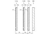
(1) 電磁波吸収体の一例
図13及び図14に示す電磁波吸収体は、電磁波反射体200の前に2枚の電磁波吸収フィルム100a,100bを誘電体を介して積層してなる。この電磁波吸収体は、第一の電磁波吸収フィルム100a/誘電体30a/第二の電磁波吸収フィルム100b/誘電体30b/電磁波反射体200の層構成を有する。各電磁波吸収フィルム100a,100bの導電体層11a,11bはプラスチックフィルム10の同じ側にあっても反対側にあっても良い。本発明では、(a) 第一及び第二の電磁波吸収フィルム100a,100bの導電体層11a,11bの表面抵抗は100〜1000Ω/□の範囲内にあり、かつ(b) 導電体層11aの表面抵抗は導電体層11bの表面抵抗より100Ω/□以上大きい必要がある。すなわち、導電体層11aの表面抵抗は200〜1000Ω/□の範囲内で、導電体層11bの表面抵抗は100〜900Ω/□の範囲内であり、かつ導電体層11aの表面抵抗は導電体層11bの表面抵抗より100Ω/□以上大きい。条件(a) 及び(b) を同時に満たさないと、高い電磁波吸収能を有さない。導電体層11a及び11bの表面抵抗は200〜1000Ω/□が好ましく、250〜800Ω/□がより好ましい。また導電体層11aの表面抵抗は導電体層11bの表面抵抗より200Ω/□以上大きいのが好ましく、300Ω/□以上大きいのがより好ましい。
(1) Example of Electromagnetic Wave Absorber The electromagnetic wave absorber shown in FIGS. 13 and 14 is formed by laminating two electromagnetic
誘電体30aの厚さは第一の電磁波吸収フィルム100aと第二の電磁波吸収フィルム100bとの間隔D1を決め、誘電体30bの厚さは第二の電磁波吸収フィルム100aと電磁波反射体200との間隔D2を決める。間隔D1/間隔D2の比は100:30〜100:70である。上記条件(a) 及び(b) を満たすとともに、間隔D1/間隔D2の比がこの範囲内である場合に、最も高い電磁波吸収能が得られる。間隔D1/間隔D2の比は100:40〜100:60が好ましく、100:45〜100:55がより好ましく、理想的には100:50である。
The thickness of the dielectric 30a knocked spacing D 1 of the the first electromagnetic
第一及び第二の電磁波吸収フィルムには、導電体層の反対側に線状痕が形成されている。図15に示すように線状痕12が電磁波吸収フィルム110a,110bの導電体層11a,11bの側に形成されている場合、及び図16に示すように線状痕12が電磁波吸収フィルム120a,120bのプラスチック面に形成されている場合のいずれも、上記条件(a) 及び(b) を満たす必要があり、かつ間隔D1/間隔D2の比は上記範囲内である必要がある。線状痕が形成されている場合も、導電体層11a及び11bの表面抵抗は100〜1000Ω/□であり、200〜1000Ω/□が好ましく、250〜800Ω/□がより好ましく、また導電体層11aの表面抵抗は導電体層11bの表面抵抗より100Ω/□以上大きく、200Ω/□以上大きいのが好ましく、300Ω/□以上大きいのがより好ましい。
In the first and second electromagnetic wave absorbing films, linear marks are formed on the opposite side of the conductor layer. As shown in FIG. 15, when the
図15に示す場合、線状痕12により電磁波吸収フィルム110a,110bの導電体層11a,11bの表面抵抗を調整でき、かつ線状痕12のギャップで電磁波が減衰するという利点が得られる。また図16に示す場合、電磁波吸収フィルム120a,120bの導電体層11a,11bの透明性が線状痕12により影響されないという利点が得られる。図15及び図16のいずれの場合も、図17に示すように第一の電磁波吸収フィルム110a(120a)/誘電体30a/第二の電磁波吸収フィルム110b(120b)/誘電体30b/電磁波反射体200の層構成を有する。
In the case shown in FIG. 15, the surface resistance of the conductor layers 11a and 11b of the electromagnetic
図18(a) 及び図18(b) は電磁波吸収体を構成する2枚の電磁波吸収フィルムの線状痕の組合せ例を示す。2枚の電磁波吸収フィルム110a(120a),110b(120b)の線状痕の配向及び交差角θsを吸収すべき周波数に応じて変えることにより、電磁波吸収能の異方性が低減し、優れた電磁波吸収能が得られる。例えば、線状痕の交差角θsが60°だと電界吸収能に優れた電磁波吸収フィルムが得られ、線状痕の交差角θsが90°だと磁界吸収能に優れた電磁波吸収フィルムが得られる。従って、例えば線状痕の交差角θsが60°の第一の電磁波吸収フィルム110a(120a)と線状痕の交差角θsが90°の第二の電磁波吸収フィルム110b(120b)とを組合せてなる図18(c) の電磁波吸収体は、電界吸収能及び磁界吸収能の両方に優れている。
FIG. 18 (a) and FIG. 18 (b) show examples of combinations of linear traces of two electromagnetic wave absorbing films constituting the electromagnetic wave absorber. By changing the orientation of the linear traces and the crossing angle θs of the two electromagnetic
(2) 電磁波吸収体の別の例
図19及び図20に示す電磁波吸収体は、電磁波反射体200の前に3枚の電磁波吸収フィルム100a,100b,100cを誘電体30a,30b,30cを介して積層してなる。この電磁波吸収体は、第一の電磁波吸収フィルム100a/誘電体30a/第二の電磁波吸収フィルム100b/誘電体30b/第三の電磁波吸収フィルム100c/誘電体30c/電磁波反射体200の層構成を有する。各電磁波吸収フィルム100a,100b,100cの導電体層11a,11b,11cは全てプラスチックフィルム10の同じ側にあっても反対側にあっても良い。本発明では、(a) 第一〜第三の電磁波吸収フィルム100a,100b,100cの導電体層11a,11b,11cの表面抵抗は100〜1000Ω/□の範囲内にあり、かつ(b) 導電体層11aの表面抵抗は導電体層11bの表面抵抗より100Ω/□以上大きい必要がある。条件(a) 及び(b) を同時に満たさないと、高い電磁波吸収能を有さない。各導電体層11a,11b,11cの表面抵抗は200〜1000Ω/□が好ましく、250〜800Ω/□がより好ましい。また導電体層11aの表面抵抗は導電体層11bの表面抵抗より200Ω/□以上大きいのが好ましく、300Ω/□以上大きいのがより好ましい。さらに導電体層11cの表面抵抗は導電体層11bの表面抵抗より50Ω/□以上大きいのが好ましく、100Ω/□以上大きいのがより好ましく、200Ω/□以上大きいのが最も好ましく、300Ω/□以上大きいのが特に好ましい。導電体層11cの表面抵抗は導電体層11aの表面抵抗と同じで良い。
(2) Another Example of Electromagnetic Wave Absorber The electromagnetic wave absorber shown in FIGS. 19 and 20 has three electromagnetic
誘電体30aの厚さは第一の電磁波吸収フィルム100aと第二の電磁波吸収フィルム100bとの間隔D1を決め、誘電体30bの厚さは第二の電磁波吸収フィルム100aと第三の電磁波吸収フィルム100cとの間隔D2を決め、誘電体30cの厚さは第三の電磁波吸収フィルム100cと電磁波反射体200との間隔D3を決める。間隔D1/間隔D2の比は100:30〜100:70である。間隔D3/間隔D2の比も100:30〜100:70であるのが好ましい。上記条件(a) 及び(b) を満たすとともに、間隔D1/間隔D2の比、及び間隔D3/間隔D2の比がこれらの範囲内である場合に、最も高い電磁波吸収能が得られる。間隔D1/間隔D2の比は100:40〜100:60が好ましく、100:45〜100:55がより好ましく、理想的には100:50である。間隔D3/間隔D2の比も100:40〜100:60がより好ましく、100:45〜100:55が最も好ましく、理想的には100:50である。間隔D1と間隔D3は同じで良い。
The thickness of the dielectric 30a knocked spacing D 1 of the the first electromagnetic
第一〜第三の電磁波吸収フィルムには、導電体層の反対側に線状痕が形成されている。図21に示すように線状痕12が電磁波吸収フィルム110a,110b,110cの導電体層11a,11b,11cの側に形成されている場合、及び図22に示すように線状痕12が電磁波吸収フィルム120a,120b,120cのプラスチック面に形成されている場合のいずれも、上記条件(a) 及び(b) を満たす必要があり、かつ間隔D1/間隔D2の比は上記範囲内である。間隔D3/間隔D2の比も上記範囲内であるのが好ましい。図21に示す場合、線状痕12により電磁波吸収フィルム110a,110b,110cの導電体層11a,11b,11cの表面抵抗を調整でき、かつ線状痕12のギャップで電磁波が減衰するという利点が得られる。また図22に示す場合、電磁波吸収フィルム120a,120bの導電体層11a,11b,11cの透明性が線状痕12により影響されないという利点が得られる。図21及び図22のいずれの場合も、図23に示すように第一の電磁波吸収フィルム110a(120a)/誘電体30a/第二の電磁波吸収フィルム110b(120b)/誘電体30b/第三の電磁波吸収フィルム110c(120c)/誘電体30c/電磁波反射体200の層構成を有する。
In the first to third electromagnetic wave absorbing films, linear marks are formed on the opposite side of the conductor layer. When the
線状痕12が形成されている場合も、各導電体層11a,11b,11cの表面抵抗は100〜1000Ω/□であり、200〜1000Ω/□が好ましく、250〜800Ω/□がより好ましく、また導電体層11aの表面抵抗は導電体層11bの表面抵抗より100Ω/□以上大きく、200Ω/□以上大きいのが好ましく、300Ω/□以上大きいのがより好ましい。さらに導電体層11cの表面抵抗は導電体層11bの表面抵抗より50Ω/□以上大きいのが好ましく、100Ω/□以上大きいのがより好ましく、200Ω/□以上大きいのが最も好ましく、300Ω/□以上大きいのが特に好ましい。導電体層11cの表面抵抗は導電体層11aの表面抵抗と同じで良い。
Sometimes
図24(a)〜図24(f) は電磁波吸収体を構成する3枚の電磁波吸収フィルムの線状痕の組合せ例を示す。3枚の電磁波吸収フィルム110a(120a),110b(120b),110c(120c)の線状痕の交差角θsを吸収すべき周波数に応じて変えることにより、優れた電磁波吸収能が得られる。
FIG. 24 (a) to FIG. 24 (f) show examples of combinations of linear marks of three electromagnetic wave absorbing films constituting the electromagnetic wave absorber. By changing the crossing angle θs of the linear marks of the three electromagnetic
図24(a) に示す例では、第一及び第三の電磁波吸収フィルム110a(120a),110c(120c)における線状痕の交差角θsは60°であり、第二の電磁波吸収フィルム110b(120b)における線状痕の交差角θsは90°である。線状痕の交差角θsが60°だと電界吸収能に優れた電磁波吸収フィルムが得られ、線状痕の交差角θsが90°だと磁界吸収能に優れた電磁波吸収フィルムが得られるので、図24(a) の電磁波吸収体は、電界吸収能及び磁界吸収能の両方に優れている。図24(b) に示す例では逆に、第一及び第三の電磁波吸収フィルム110a(120a),110c(120c)における線状痕の交差角θsは90°であり、第二の電磁波吸収フィルム110b(120b)における線状痕の交差角θsは60°である。この例の電磁波吸収体も電界吸収能及び磁界吸収能の両方に優れている。
In the example shown in FIG. 24 (a), the crossing angle θs of the linear marks in the first and third electromagnetic
図24(c) に示す例では、第一〜第三の電磁波吸収フィルム110a(120a),110b(120b),110c(120c)における線状痕の交差角θsは全て90°である。この場合、第一及び第三の電磁波吸収フィルム110a(120a),110c(120c)における線状痕と第二の電磁波吸収フィルム110b(120b)における線状痕とは45°で交差しているのが好ましい。この例の電磁波吸収体は優れた磁界吸収能を有する。
In the example shown in FIG. 24 (c), the crossing angles θs of the linear marks in the first to third electromagnetic
図24(d) に示す例では、第一〜第三の電磁波吸収フィルム110a(120a),110b(120b),110c(120c)における線状痕の交差角θsは全て60°である。この場合、第一及び第三の電磁波吸収フィルム110a(120a),110c(120c)における線状痕の方向と第二の電磁波吸収フィルム110b(120b)における線状痕の方向とは直交しているのが好ましい。この例の電磁波吸収体は優れた電界吸収能を有する。
In the example shown in FIG. 24 (d), the crossing angles θs of the linear marks in the first to third electromagnetic
図24(e) 及び図24(f) に示す例では、線状痕の交差角θsが90°の電磁波吸収フィルムと線状痕の交差角θsが45°の電磁波吸収フィルムとの組合せである。線状痕の交差角θsが60°の電磁波吸収フィルムの代わりに線状痕の交差角θsが45°の電磁波吸収フィルムを用いても、良好な電界吸収能及び磁界吸収能を有する電磁波吸収体が得られる。 In the example shown in FIG. 24 (e) and FIG. 24 (f), a combination of an electromagnetic wave absorbing film having a linear trace crossing angle θs of 90 ° and an electromagnetic wave absorbing film having a linear trace crossing angle θs of 45 ° is used. . Even if an electromagnetic wave absorbing film having a crossing angle θs of 45 degrees is used instead of an electromagnetic wave absorbing film having a line mark crossing angle θs of 60 °, the electromagnetic wave absorber has good electric field absorption ability and magnetic field absorption ability. Is obtained.
例示の電磁波吸収フィルム110a(120a),110b(120b),110c(120c)の線状痕交差角θsは45°,60°及び90°であったが、本発明は勿論これらに限定されず、30〜90°以内の他の交差角θsも使用可能である。研究の結果、交差角θsは360/偶数であるのが好ましいことが分った。従って、30°,36°,45°,60°及び90°が好ましい。ここで、交差角θsには製造誤差があるので、一般に目標値の±5°以内、好ましくは±3°以内であれば良い。例えば交差角θsが60°の場合、55〜65°の範囲内であれば良い。また交差角θsが90°の場合、85〜90°の範囲内であれば良い。三層の電磁波吸収フィルムを有する電磁波吸収体の場合、外側の電磁波吸収フィルムの線状痕交差角θsは60°又は90°であるのが好ましい。
The linear mark crossing angles θs of the exemplary electromagnetic
本発明を以下の実施例によりさらに詳細に説明するが、本発明はそれらに限定されるものではない。 The present invention will be described in more detail with reference to the following examples, but the present invention is not limited thereto.
比較例1
図13に示す電磁波吸収体の試験片TP(32 cm×52 cm)を、厚さ120μmのPETフィルム10aに厚さ10 nmのNi薄膜11aを形成してなる電磁波吸収フィルム100a(表面抵抗:785Ω)と、厚さ120μmのPETフィルム10bに厚さ15 nmのNi薄膜11bを形成してなる電磁波吸収フィルム100b(表面抵抗:283Ω)と、厚さ2 mmのアルミニウム板200により構成した。電磁波吸収フィルム100aと電磁波吸収フィルム100bとの間隔D1は20 mmであり、電磁波吸収フィルム100bとアルミニウム板200との間隔D2は10 mmであった。
Comparative Example 1
An electromagnetic
この試験片TPの電磁波吸収能を図25に示す装置を用いて評価した。この装置は、厚さ2 cmの誘電体ホルダ62と、ホルダ62から100 cm離れた送信アンテナ63a及び受信アンテナ63bと、アンテナ63a,63bに接続したネットワークアナライザ64とを有する。まずホルダ62の前面(アンテナ側)にアルミニウム板(32 cm×52 cm×2 mm)を固定し、アンテナ63aから10°から60°まで10°間隔で入射角度θiを変えながら、1〜5.5 GHzの周波数の電磁波(円偏波)を0.25 GHzの周波数間隔で照射し、アンテナ63bで反射波を受信し、ネットワークアナライザ64により反射電力を測定した。次にアルミニウム板の代わりに試験片TPをホルダ62の前面に固定し、上記と同様にして反射電力を測定した。アルミニウム板を用いて測定した反射電力が入射電力と等しいと仮定し、反射係数(反射電力/入射電力)RCを求め、RL(dB)=20 log(1/RC)により反射減衰量(リターンロス)RL(dB)を求めた。各入射角度θiにおける反射減衰量は周波数に応じて変化するので、反射減衰量が最大となるときの周波数(ピーク周波数)で得られた電磁波吸収率をピーク吸収率とした。
The electromagnetic wave absorbing ability of this test piece TP was evaluated using the apparatus shown in FIG. This apparatus includes a
測定したピーク吸収率及びピーク周波数をそれぞれ図26に示す。図26から明らかなように、10〜60°の入射角度範囲でTE波のピーク吸収率は約13〜38 dBであり、またTM波のピーク吸収率は約11〜49 dBであった。この結果から、前面側に高抵抗のNi薄膜11aを有する電磁波吸収フィルム100aを配置し、後面側に低抵抗のNi薄膜11bを有する電磁波吸収フィルム100bを配置し、D1/D2の比を2/1とした電磁波吸収体は高い電磁波吸収能を有することが分かった。
The measured peak absorption rate and peak frequency are shown in FIG. As is apparent from FIG. 26, the TE wave peak absorptance was about 13 to 38 dB and the TM wave peak absorptance was about 11 to 49 dB in the incident angle range of 10 to 60 °. From this result, the electromagnetic
実施例1
比較例1で用いた電磁波吸収フィルム100aに対して、粒径分布が50〜80μmのダイヤモンド微粒子を電着したパターンロール32a,32bを有する図12に示す構造の装置を用い、プラスチック面(Ni薄膜11aが形成されていない面)に交差角が90°の二方向の線状痕を形成した。また比較例1で用いた電磁波吸収フィルム100bに対して、粒径分布が50〜80μmのダイヤモンド微粒子を電着したパターンロール2a,2bを有する図8(a) に示す構造の装置を用い、プラスチック面(Ni薄膜11bが形成されていない面)に交差角が60°の二方向の線状痕を形成した。得られた線状痕付き電磁波吸収フィルム120a,120bにおける線状痕の特性は下記の通りであった。
幅Wの範囲:0.5〜5μm
平均幅Wav:2μm
横手方向間隔Iの範囲:2〜30μm
平均横手方向間隔Iav:10μm
平均長さLav:5 mm
交差角θs:90°及び60°
Example 1
For the electromagnetic
Width W range: 0.5-5μm
Average width Wav: 2μm
Range in the lateral direction I: 2 to 30 μm
Average lateral direction interval Iav: 10μm
Average length Lav: 5 mm
Crossing angle θs: 90 ° and 60 °
これらの線状痕付きの電磁波吸収フィルム120a,120bを使用した以外比較例1と同様にして図16に示す電磁波吸収体を作製し、10°〜60°の入射角度範囲でそのピーク吸収率及びピーク周波数を測定した。結果を図27に示す。図27から明らかなように、TE波のピーク吸収率は約15〜54 dBであり、またTM波のピーク吸収率は約12〜36 dBであった。また、この入射角度範囲でTE波のピーク吸収率は全体的に比較例1より高かった。この結果から、高抵抗のNi薄膜11aを有する電磁波吸収フィルム120aが前面側で、低抵抗のNi薄膜11bを有する電磁波吸収フィルム120bが後面側であり、D1/D2の比が2/1であり、各電磁波吸収フィルム120a,120bのプラスチック面側に二方向の線状痕を有する電磁波吸収体は、線状痕を形成していない比較例1の電磁波吸収体より高い電磁波吸収能を有することが分かった。
The electromagnetic wave absorber shown in FIG. 16 was prepared in the same manner as in Comparative Example 1 except that these electromagnetic
比較例2
比較例1と別に厚さ120μmのPETフィルム10a上に形成した厚さ10 nmのNi薄膜11aは500Ωの表面抵抗を有していた。この電磁波吸収フィルム100aを前面側に用いた以外比較例1と同様にして、電磁波吸収体を作製し、10°〜60°の入射角度範囲でピーク吸収率及びピーク周波数を比較例1と同様に測定した。結果を図28に示す。図28から明らかなように、TE波のピーク吸収率は約14〜37 dBであり、またTM波のピーク吸収率は約12〜36 dBであった。この結果から、前面側に高抵抗のNi薄膜11aを有する電磁波吸収フィルム100aを配置し、後面側に低抵抗のNi薄膜11bを有する電磁波吸収フィルム100bを配置し、D1/D2の比を2/1とした電磁波吸収体は高い電磁波吸収能を有することが分かった。
Comparative Example 2
Separately from Comparative Example 1 , the 10 nm thick Ni
実施例2
比較例2で用いた電磁波吸収フィルム100aのプラスチック面(Ni薄膜11aが形成されていない面)に、実施例1と同様にして交差角が90°の二方向の線状痕を形成した。また比較例2で用いた電磁波吸収フィルム100bのプラスチック面(Ni薄膜11bが形成されていない面)に、実施例1と同様にして交差角が60°の二方向の線状痕を形成した。これらの線状痕付きの電磁波吸収フィルム120a,120bを使用した以外比較例1と同様にして図16に示す電磁波吸収体を作製し、10°〜60°の入射角度範囲でそのピーク吸収率及びピーク周波数を測定した。結果を図29に示す。図29から明らかなように、TE波のピーク吸収率は約15〜55 dBであり、またTM波のピーク吸収率は約12〜34 dBであった。また、この入射角度範囲でTE波のピーク吸収率は全体的に比較例2より高かった。この結果から、高抵抗のNi薄膜11aを有する電磁波吸収フィルム120aが前面側で、低抵抗のNi薄膜11bを有する電磁波吸収フィルム120bが後面側であり、D1/D2の比が2/1であり、各電磁波吸収フィルム120a,120bのプラスチック面側に二方向の線状痕を有する電磁波吸収体は、線状痕を形成していない比較例2の電磁波吸収体より高い電磁波吸収能を有することが分かった。
Example 2
In the same manner as in Example 1 , two-way linear traces having an intersecting angle of 90 ° were formed on the plastic surface (the surface on which the Ni
比較例3
比較例1と別に厚さ120μmのPETフィルム10b上に形成した厚さ10 nmのNi薄膜11bは300Ωの表面抵抗を有していた。この電磁波吸収フィルム100bを後面側に用いた以外比較例1と同様に電磁波吸収体を作製し、10°〜60°の入射角度範囲でピーク吸収率及びピーク周波数を比較例1と同様に測定した。結果を図30に示す。図30から明らかなように、TE波のピーク吸収率は約14〜46 dBであり、またTM波のピーク吸収率は約12〜42 dBであった。この結果から、前面側に高抵抗のNi薄膜11aを有する電磁波吸収フィルム100aを配置し、後面側に低抵抗のNi薄膜11bを有する電磁波吸収フィルム100bを配置し、D1/D2の比を2/1とした電磁波吸収体は高い電磁波吸収能を有することが分かった。
Comparative Example 3
Separately from Comparative Example 1 , a 10 nm thick Ni
比較例4
電磁波吸収フィルム100aと電磁波吸収フィルム100bとの間隔D1を10 mmとし、電磁波吸収フィルム100bとアルミニウム板200との間隔D2を20 mmとし、D1/D2の比を1/2とした以外比較例3と同様に電磁波吸収体を作製し、10°〜60°の入射角度範囲でピーク吸収率及びピーク周波数を比較例1と同様に測定した。結果を図31に示す。図31から明らかなように、TE波のピーク吸収率は約8〜15 dBであり、またTM波のピーク吸収率は約15〜32 dBであった。この入射角度範囲でTE波及びTM波のピーク吸収率は全体的に比較例3より低かった。この結果から、D1/D2の比が2/1から1/2になると、電磁波吸収体の電磁波吸収能は比較的低下することが分かった。これから、前面側の電磁波吸収フィルム100aが後面側の電磁波吸収フィルム100bより高抵抗の場合に、電磁波吸収フィルム100aと電磁波吸収フィルム100bとの間隔D1が電磁波吸収フィルム100bと反射板200との間隔D2より大きい方が電磁波吸収体の電磁波吸収能が高いことが分かる。
Comparative Example 4
The distance D 1 between the electromagnetic
比較例5
電磁波吸収フィルム100aと電磁波吸収フィルム100bとの間隔D1を15 mmとし、電磁波吸収フィルム100bとアルミニウム板200との間隔D2を15 mmとし、D1/D2の比を1/1とした以外比較例3と同様に電磁波吸収体を作製し、10°〜60°の入射角度範囲でピーク吸収率及びピーク周波数を比較例1と同様に測定した。結果を図32に示す。図32から明らかなように、TE波のピーク吸収率は約16〜20 dBであり、またTM波のピーク吸収率は約20〜34 dBであった。この結果から、D1/D2の比が2/1から1/1になると、電磁波吸収体の電磁波吸収能は比較的低下することが分かった。しかし、電磁波吸収能の低下の程度はD1/D2の比が1/2になった比較例4より小さかった。
Comparative Example 5
The distance D 1 between the electromagnetic
比較例6
表面抵抗が300Ωの電磁波吸収フィルムを前面側の電磁波吸収フィルム100aとし、表面抵抗が785Ωの電磁波吸収フィルムを後面側の電磁波吸収フィルム100bとした以外比較例3と同様に電磁波吸収体を作製し、10°〜60°の入射角度範囲でピーク吸収率及びピーク周波数を比較例1と同様に測定した。結果を図33に示す。図33から明らかなように、TE波のピーク吸収率は約10〜17 dBであり、またTM波のピーク吸収率は約12〜52 dBであった。この結果から、前面側の電磁波吸収フィルム100aを後面側の電磁波吸収フィルム100bより低抵抗にすると、電磁波吸収体の電磁波吸収能は不十分なレベルまで低下することが分かる。
Comparative Example 6
An electromagnetic wave absorber was prepared in the same manner as in Comparative Example 3 except that an electromagnetic wave absorbing film having a surface resistance of 300Ω was used as the front electromagnetic
比較例7
電磁波吸収フィルム100aと電磁波吸収フィルム100bとの間隔D1を10 mmとし、電磁波吸収フィルム100bとアルミニウム板200との間隔D2を20 mmとし、D1/D2の比を1/2とした以外比較例6と同様に電磁波吸収体を作製し、10°〜60°の入射角度範囲でピーク吸収率及びピーク周波数を比較例1と同様に測定した。結果を図34に示す。図34から明らかなように、TE波のピーク吸収率は約8〜12 dBであり、またTM波のピーク吸収率は約12〜50 dBであった。この結果から、前面側の電磁波吸収フィルム100aが後面側の電磁波吸収フィルム100bより低抵抗の場合に、D1/D2の比が2/1から1/2になると、電磁波吸収体の電磁波吸収能はさらに低下することが分かった。
Comparative Example 7
The distance D 1 between the electromagnetic
比較例8
電磁波吸収フィルム100aと電磁波吸収フィルム100bとの間隔D1を15 mmとし、電磁波吸収フィルム100bとアルミニウム板200との間隔D2を15 mmとし、D1/D2の比を1/1とした以外比較例6と同様に電磁波吸収体を作製し、10°〜60°の入射角度範囲でピーク吸収率及びピーク周波数を比較例1と同様に測定した。結果を図35に示す。図35から明らかなように、TE波のピーク吸収率は約7〜14 dBであり、またTM波のピーク吸収率は約16〜32 dBであった。この結果から、前面側の電磁波吸収フィルム100aが後面側の電磁波吸収フィルム100bより低抵抗の場合に、D1/D2の比が2/1から1/1になると、電磁波吸収体の電磁波吸収能はさらに低下することが分かった。しかし、電磁波吸収能の低下の程度はD1/D2の比が1/2になった比較例7より小さかった。
Comparative Example 8
The distance D 1 between the electromagnetic
実施例3
表面抵抗が785Ωの電磁波吸収フィルム100aのプラスチック面に対して実施例1と同様にして交差角が60°の二方向の線状痕を形成した。また表面抵抗が300Ωの電磁波吸収フィルム100bのプラスチック面に対して実施例1と同様にして交差角が90°の二方向の線状痕を形成した。これらの線状痕付きの電磁波吸収フィルム120a,120bを使用した以外比較例3と同様にして図16に示す電磁波吸収体を作製し、10°〜60°の入射角度範囲でそのピーク吸収率及びピーク周波数を測定した。結果を図36に示す。図36から明らかなように、TE波のピーク吸収率は約12〜22 dBであり、またTM波のピーク吸収率は約15〜42 dBであった。この入射角度範囲でTE波及びTM波のピーク吸収率の異方性は比較例3より小さかった。この結果から、高抵抗のNi薄膜11aを有する電磁波吸収フィルム120aが前面側で、低抵抗のNi薄膜11bを有する電磁波吸収フィルム120bが後面側であり、D1/D2の比が2/1であり、各電磁波吸収フィルム120a,120bのプラスチック面側に二方向の線状痕を有する電磁波吸収体は、小さい異方性で高い電磁波吸収能を有することが分かった。
Example 3
Bidirectional traces having a crossing angle of 60 ° were formed on the plastic surface of the electromagnetic
実施例4
D1を4 mmとし、D2を2 mmとした以外実施例3と同じ電磁波吸収体を作製し、10°〜60°の入射角度範囲で5.8 GHzにおける電磁波吸収率を測定した。結果を図37に示す。図37から明らかなように、TE波の電磁波吸収率は約12〜52 dBであり、またTM波の電磁波吸収率は約4〜25 dBであった。この結果から、D1及びD2が小さくても、高抵抗のNi薄膜11aを有する電磁波吸収フィルム120aが前面側で、低抵抗のNi薄膜11bを有する電磁波吸収フィルム120bが後面側であり、D1/D2の比が2/1であり、各電磁波吸収フィルム120a,120bのプラスチック面側に二方向の線状痕を有する電磁波吸収体は、高い電磁波吸収能を有することが分かった。
Example 4
The same electromagnetic wave absorber as in Example 3 was prepared except that D1 was 4 mm and D2 was 2 mm, and the electromagnetic wave absorption rate at 5.8 GHz was measured in an incident angle range of 10 ° to 60 °. The results are shown in FIG. As is apparent from FIG. 37, the electromagnetic wave absorption rate of the TE wave was about 12 to 52 dB, and the electromagnetic wave absorption rate of the TM wave was about 4 to 25 dB. From this result, even if D1 and D2 are small, the electromagnetic
実施例5
実施例1と同じ方法により表面抵抗が300Ωの電磁波吸収フィルムのプラスチック面に交差角が45°の二方向の線状痕を形成し、電磁波吸収フィルム120bを作製した。交差角が90°の二方向の線状痕を形成した表面抵抗が785Ωの電磁波吸収フィルム120aと上記電磁波吸収フィルム120bとを組合せた以外実施例4と同じ構造の電磁波吸収体を作製し、10°〜60°の入射角度範囲で5.8 GHzにおける電磁波吸収率を測定した。結果を図38に示す。図38から明らかなように、TE波の電磁波吸収率は約16〜37 dBであり、またTM波の電磁波吸収率は約4〜28 dBであった。この結果から、一方の電磁波吸収フィルムの線状痕の交差角が45°で、D1及びD2が小さくても、高抵抗のNi薄膜11aを有する電磁波吸収フィルム120aが前面側で、低抵抗のNi薄膜11bを有する電磁波吸収フィルム120bが後面側であり、D1/D2の比が2/1であり、各電磁波吸収フィルム120a,120bのプラスチック面側に二方向の線状痕を有する電磁波吸収体は、高い電磁波吸収能を有することが分かった。
Example 5
In the same manner as in Example 1 , two-way linear marks having a crossing angle of 45 ° were formed on the plastic surface of the electromagnetic wave absorbing film having a surface resistance of 300Ω to produce the electromagnetic
比較例9
電磁波吸収フィルム120aと電磁波吸収フィルム120bとの間隔D1を10 mmとし、電磁波吸収フィルム120bとアルミニウム板200との間隔D2を20 mmとし、D1/D2の比を1/2とした以外実施例3と同様にして、図16に示す電磁波吸収体を作製した。10°〜60°の入射角度範囲で、この電磁波吸収体のピーク吸収率及びピーク周波数を比較例1と同様に測定した。結果を図39に示す。図39から明らかなように、TE波のピーク吸収率は約8〜16 dBであり、またTM波のピーク吸収率は約17〜28 dBであった。この結果から、D1/D2の比が2/1から1/2になると、電磁波吸収体の電磁波吸収能は比較的低下することが分かった。これから、前面側の電磁波吸収フィルム120aが後面側の電磁波吸収フィルム120bより高抵抗の場合に、電磁波吸収フィルム120aと電磁波吸収フィルム120bとの間隔D1が電磁波吸収フィルム120bと反射板200との間隔D2より大きい方が電磁波吸収体の電磁波吸収能が高いことが分かる。
Comparative Example 9
The distance D 1 between the electromagnetic
比較例10
電磁波吸収フィルム120aと電磁波吸収フィルム120bとの間隔D1を15 mmとし、電磁波吸収フィルム120bとアルミニウム板200との間隔D2を15 mmとし、D1/D2の比を1/1とした以外実施例3と同様にして、図16に示す電磁波吸収体を作製した。10°〜60°の入射角度範囲で、この電磁波吸収体のピーク吸収率及びピーク周波数を比較例1と同様に測定した。結果を図40に示す。図40から明らかなように、TE波のピーク吸収率は約12〜22 dBであり、またTM波のピーク吸収率は約15〜42 dBであった。この結果から、D1/D2の比が2/1から1/1になると、電磁波吸収体の電磁波吸収能は比較的低下することが分かった。しかし、電磁波吸収能の低下の程度はD1/D2の比が1/2になった比較例9より小さかった。
Comparative Example 10
The distance D 1 between the electromagnetic
比較例11
電磁波吸収フィルム100aの表面抵抗を300Ωとし、電磁波吸収フィルム100bの表面抵抗を785Ωとした以外実施例3と同じ構成の電磁波吸収体を作製し、10°〜60°の入射角度範囲でピーク吸収率及びピーク周波数を比較例1と同様に測定した。結果を図41に示す。図41から明らかなように、TE波のピーク吸収率は約11〜18 dBであり、またTM波のピーク吸収率は約15〜36 dBであった。この結果から、前面側の電磁波吸収フィルム100aの表面抵抗が後面側の電磁波吸収フィルム100bの表面抵抗より小さいと、線状痕を形成しても十分に高い電磁波吸収能が得られないことが分かる。
Comparative Example 11
An electromagnetic wave absorber having the same structure as in Example 3 was prepared except that the surface resistance of the electromagnetic
比較例12
比較例1の電磁波吸収体の電磁波吸収フィルム100bとアルミニウム板200との間に電磁波吸収フィルム100aと同じ電磁波吸収フィルム100cを配置し、電磁波吸収フィルム100aと電磁波吸収フィルム100bとの間隔D1と、電磁波吸収フィルム100bと電磁波吸収フィルム100cとの間隔D2と、電磁波吸収フィルム100cとアルミニウム板200との間隔D3をそれぞれ20 mm、10 mm、及び20 mmとし、D1/D2/D3を2/1/2として、図19に示す電磁波吸収体を作製した。10°〜60°の入射角度範囲で、この電磁波吸収体のピーク吸収率及びピーク周波数を比較例1と同様に測定した。結果を図42に示す。図42から明らかなように、TE波のピーク吸収率は約12〜28 dBであり、またTM波のピーク吸収率は約26〜36 dBであった。また、この入射角度範囲でTM波のピーク吸収率は全体的に高かった。この結果から、三枚の電磁波吸収フィルムを有する電磁波吸収体の場合でも、最前の電磁波吸収フィルム100aの表面抵抗が二枚目の電磁波吸収フィルム100bの表面抵抗より大きければ、優れた電磁波吸収能を示すことが分かる。またD1/D2の比を2/1とし、D3/D2の比を2/1とするのは、高い電磁波吸収能を得るのに好ましいことも分かる。
Comparative Example 12
The same electromagnetic
比較例13
間隔D1、D2及びD3をそれぞれ10 mm、10 mm及び30 mmとし、D1/D2/D3の比を1/1/3とした以外比較例12と同様にして、図19に示す電磁波吸収体を作製した。10°〜60°の入射角度範囲で、この電磁波吸収体のピーク吸収率及びピーク周波数を比較例1と同様に測定した。結果を図43に示す。図43から明らかなように、TE波のピーク吸収率は約12〜28 dBであり、またTM波のピーク吸収率は約26〜36 dBであった。この結果から、三枚の電磁波吸収フィルムを有する電磁波吸収体の場合でも、最前の電磁波吸収フィルム100aの表面抵抗が二枚目の電磁波吸収フィルム100bの表面抵抗より大きければ、優れた電磁波吸収能を示すことが分かる。
Comparative Example 13
The distances D 1 , D 2 and D 3 were 10 mm, 10 mm and 30 mm, respectively, and the ratio of D 1 / D 2 / D 3 was 1/1/3, as in Comparative Example 12, and FIG. The electromagnetic wave absorber shown in FIG. In the incident angle range of 10 ° to 60 °, the peak absorption rate and peak frequency of this electromagnetic wave absorber were measured in the same manner as in Comparative Example 1 . The results are shown in FIG. As is clear from FIG. 43, the TE wave peak absorptance was about 12 to 28 dB, and the TM wave peak absorptance was about 26 to 36 dB. From this result, even in the case of an electromagnetic wave absorber having three electromagnetic wave absorbing films, if the surface resistance of the first electromagnetic
比較例14
電磁波吸収フィルム100a、電磁波吸収フィルム100b、及び電磁波吸収フィルム100cの表面抵抗をそれぞれ283Ω、785Ω及び283Ωとした以外比較例12と同様にして、図19に示す電磁波吸収体を作製した。10°〜60°の入射角度範囲で、この電磁波吸収体のピーク吸収率及びピーク周波数を比較例1と同様に測定した。結果を図44に示す。図44から明らかなように、TE波のピーク吸収率は約8〜15 dBであり、またTM波のピーク吸収率は約15〜27 dBであった。この結果から、三枚の電磁波吸収フィルムを有する電磁波吸収体の場合でも、最前の電磁波吸収フィルム100aの表面抵抗が二枚目の電磁波吸収フィルム100bの表面抵抗より小さければ、十分に高い電磁波吸収能が得られないことが分かる。
Comparative Example 14
An electromagnetic wave absorber shown in FIG. 19 was produced in the same manner as in Comparative Example 12 except that the surface resistances of the electromagnetic
実施例6
電磁波吸収フィルム100a、電磁波吸収フィルム100b、及び電磁波吸収フィルム100cのプラスチック面にそれぞれ交差角が60°,90°及び60°の二方向の線状痕を形成した以外比較例12と同様にして、図22に示す電磁波吸収体を作製した。10°〜60°の入射角度範囲で、この電磁波吸収体のピーク吸収率及びピーク周波数を比較例1と同様に測定した。結果を図45に示す。図45から明らかなように、TE波のピーク吸収率は12〜32 dBであり、またTM波のピーク吸収率は約22〜52 dBであった。この入射角度範囲でTM波のピーク吸収率は全体的に高かった。この結果から、三枚の電磁波吸収フィルムを有する電磁波吸収体の場合でも、最前の電磁波吸収フィルム100aの表面抵抗が二枚目の電磁波吸収フィルム100bの表面抵抗より大きければ、優れた電磁波吸収能を示すことが分かる。またD1/D2の比を2/1とし、D3/D2の比を2/1とするのは、高い電磁波吸収能を得るのに好ましいことも分かる。
Example 6
Electromagnetic
比較例15
間隔D1、D2及びD3をそれぞれ20 mm、20 mm及び20 mmとし、D1/D2/D3の比を1/1/1とした以外実施例6と同様にして、図22に示す電磁波吸収体を作製した。10°〜60°の入射角度範囲で、この電磁波吸収体のピーク吸収率及びピーク周波数を比較例1と同様に測定した。結果を図46に示す。図46から明らかなように、TE波のピーク吸収率は約13〜43 dBであり、またTM波のピーク吸収率は約16〜39 dBであった。この結果から、三枚の電磁波吸収フィルムを有する電磁波吸収体の場合でも、最前の電磁波吸収フィルム100aの表面抵抗が二枚目の電磁波吸収フィルム100bの表面抵抗より大きければ、優れた電磁波吸収能を示すことが分かる。ただし、D1/D2の比が2/1で、D3/D2の比が2/1の実施例6より電磁波吸収能は劣っていた。
Comparative Example 15
The intervals D 1 , D 2, and D 3 were 20 mm, 20 mm, and 20 mm, respectively, and the ratio of D 1 / D 2 / D 3 was 1/1/1, as in Example 6, and FIG. The electromagnetic wave absorber shown in FIG. In the incident angle range of 10 ° to 60 °, the peak absorption rate and peak frequency of this electromagnetic wave absorber were measured in the same manner as in Comparative Example 1 . The results are shown in FIG. As is clear from FIG. 46, the TE wave peak absorptance was about 13 to 43 dB, and the TM wave peak absorptance was about 16 to 39 dB. From this result, even in the case of an electromagnetic wave absorber having three electromagnetic wave absorbing films, if the surface resistance of the first electromagnetic
比較例16
電磁波吸収フィルム120a、電磁波吸収フィルム120b、及び電磁波吸収フィルム120cの表面抵抗をそれぞれ283Ω、785Ω及び283Ωとした以外実施例6と同様に図22に示す電磁波吸収体を作製し、10°〜60°の入射角度範囲でピーク吸収率及びピーク周波数を比較例1と同様に測定した。結果を図47に示す。図47から明らかなように、TE波のピーク吸収率は約8〜17 dBであり、またTM波のピーク吸収率は約17〜25 dBであった。この結果から、線状痕を有する三枚の電磁波吸収フィルムを有する電磁波吸収体の場合でも、最前の電磁波吸収フィルム120aの表面抵抗が二枚目の電磁波吸収フィルム120bの表面抵抗より小さければ、十分に高い電磁波吸収能が得られないことが分かる。
Comparative Example 16
The electromagnetic wave absorber shown in FIG. 22 was prepared in the same manner as in Example 6 except that the surface resistances of the electromagnetic
比較例17
電磁波吸収フィルム100aの表面抵抗を228Ωとし、電磁波吸収フィルム100bの表面抵抗を137Ω(Ni薄膜の厚さ20 nm)とした以外比較例1と同じ構成の電磁波吸収体を作製し、10°〜60°の入射角度範囲でピーク吸収率及びピーク周波数を比較例1と同様に測定した。結果を図48に示す。図48から明らかなように、TE波のピーク吸収率は約10〜38 dBであり、またTM波のピーク吸収率は約15〜45 dBであった。また10°〜60°の入射角度範囲で2.5 GHzにおける電磁波吸収率を測定した。結果を図49に示す。図49から明らかなように、TE波の吸収率は約7〜16 dBであり、またTM波のピーク吸収率は約5〜23 dBであった。これらの結果から、前面側の電磁波吸収フィルム100aの表面抵抗が後面側の電磁波吸収フィルム100bの表面抵抗より50Ω以上大きいと、十分に高い電磁波吸収能が得られることが分かる。
Comparative Example 17
An electromagnetic wave absorber having the same structure as Comparative Example 1 was prepared except that the surface resistance of the electromagnetic
比較例18
電磁波吸収フィルム100aと電磁波吸収フィルム100bの配置順序を逆にした以外比較例17と同じ構成の電磁波吸収体を作製し、10°〜60°の入射角度範囲でピーク吸収率及びピーク周波数を比較例1と同様に測定した。結果を図50に示す。図50から明らかなように、TE波のピーク吸収率は約6〜8 dBであり、またTM波のピーク吸収率は約8〜22 dBであった。また10°〜60°の入射角度範囲で2.5 GHzにおける電磁波吸収率を測定した。結果を図51に示す。図51から明らかなように、TE波の吸収率は約5.5〜7.5 dBであり、またTM波のピーク吸収率は約7.5〜11.5 dBであった。これらの結果から、前面側の電磁波吸収フィルム100aの表面抵抗が後面側の電磁波吸収フィルム100bの表面抵抗より小さいと、十分に高い電磁波吸収能が得られないことが分かる。
Comparative Example 18
An electromagnetic wave absorber having the same configuration as that of Comparative Example 17 except that the arrangement order of the electromagnetic
比較例19
電磁波吸収フィルムの表面抵抗を500Ωとし、電磁波吸収フィルム100bの表面抵抗を300Ωとした以外比較例1と同じ構成の電磁波吸収体を作製し、10°〜60°の入射角度範囲で2.5 GHzにおける電磁波吸収率を測定した。結果を図52に示す。図52から明らかなように、TE波の吸収率は約12〜27 dBであり、またTM波のピーク吸収率は約4〜25 dBであった。これらの結果から、前面側の電磁波吸収フィルム100aの表面抵抗が後面側の電磁波吸収フィルム100bの表面抵抗より大きいと、2.5 GHzにおいて十分に高い電磁波吸収能が得られることが分かる。
Comparative Example 19
An electromagnetic wave absorber having the same structure as Comparative Example 1 except that the surface resistance of the electromagnetic wave absorbing film was set to 500Ω and the surface resistance of the electromagnetic
実施例7
電磁波吸収フィルム100aのプラスチック面に交差角が60°の二方向の線状痕を形成し、電磁波吸収フィルム100bのプラスチック面に交差角が90°の二方向の線状痕を形成した以外比較例19と同じ構成の電磁波吸収体を作製し、10°〜60°の入射角度範囲で5.8 GHzにおける電磁波吸収率を測定した。結果を図53に示す。図53から明らかなように、TE波の電磁波吸収率は約17〜53 dBであり、またTM波の電磁波吸収率は約4〜26 dBであった。この結果から、前面側の電磁波吸収フィルム100aの表面抵抗が後面側の電磁波吸収フィルム100bの表面抵抗より大きいと、線状痕を形成した場合でも、5.8 GHzにおいて十分に高い電磁波吸収能が得られることが分かる。
Example 7
Comparative example except that a two-way linear mark with a crossing angle of 60 ° is formed on the plastic surface of the electromagnetic
比較例20
図6(a) に示すように、785Ωの表面抵抗を有する2枚の電磁波吸収フィルム片100a’と283Ωの表面抵抗を有する1枚の電磁波吸収フィルム片100b’とを隙間なく並べて、443Ωの平均表面抵抗を有する複合電磁波吸収フィルム130aを作製した。同様に、283Ωの表面抵抗を有する2枚の電磁波吸収フィルム片100a’と783Ωの表面抵抗を有する1枚の電磁波吸収フィルム片100b’とを隙間なく並べて、367Ωの平均表面抵抗を有する複合電磁波吸収フィルム130bを作製した。これらの複合電磁波吸収フィルム130a,130bを用いた以外比較例1と同じ構成の電磁波吸収体を作製し、10°〜60°の入射角度範囲で2.5 GHzにおける電磁波吸収率を測定した。結果を図54に示す。図54から明らかなように、TE波の電磁波吸収率は約12〜33 dBであり、またTM波の電磁波吸収率は約3〜19 dBであった。また10°〜60°の入射角度範囲でピーク吸収率及びピーク周波数を比較例1と同様に測定した。結果を図55に示す。図55から明らかなように、TE波のピーク吸収率は約16〜40 dBであり、またTM波のピーク吸収率は約11〜22 dBであった。これらの結果から、複数枚の電磁波吸収フィルム片からなる複合電磁波吸収フィルムを使用しても、前面側の複合電磁波吸収フィルム130aの表面抵抗が後面側の複合電磁波吸収フィルム130bの表面抵抗より大きいと、十分に高い電磁波吸収能が得られることが分かる。
Comparative Example 20
As shown in FIG. 6 (a), two electromagnetic wave absorbing
比較例21
図6(a) に示すように、300Ωの表面抵抗を有する2枚の電磁波吸収フィルム片100a’と500Ωの表面抵抗を有する1枚の電磁波吸収フィルム片100b’とを隙間なく並べて、331Ωの平均表面抵抗を有する複合電磁波吸収フィルム130bを作製した。比較例20で作製した443Ωの平均表面抵抗を有する複合電磁波吸収フィルム130aを、331Ωの平均表面抵抗を有する上記複合電磁波吸収フィルム130bと組合せた以外比較例20と同じ構成の電磁波吸収体を作製し、10°〜60°の入射角度範囲でピーク吸収率及びピーク周波数を比較例1と同様に測定した。結果を図56に示す。図56から明らかなように、TE波のピーク吸収率は約16〜41 dBであり、またTM波のピーク吸収率は約10〜21 dBであった。比較例20のピーク吸収率と比較すると、比較例21のピーク吸収率の方が僅かに高かった。これらの結果から、前面側の複合電磁波吸収フィルム130aの表面抵抗が後面側の複合電磁波吸収フィルム130bの表面抵抗より100Ω以上大きいと、さらに高い電磁波吸収能が得られることが分かる。
Comparative Example 21
As shown in FIG. 6 (a), two electromagnetic wave absorbing
実施例及び比較例の電磁波吸収体の構成を下記の表1に纏めて示す。

表1(続き)
以上本発明を図面を参照して詳細に説明したが、勿論本発明はそれらに限定されず、本発明の範囲内で種々の変更を施すことができる。例えば、線状痕のない電磁波吸収フィルム同士、又は線状痕を有する電磁波吸収フィルム同士の組合せだけでなく、線状痕のない電磁波吸収フィルムと線状痕を有する電磁波吸収フィルムとを組合せるのも本発明の範囲内である。 Although the present invention has been described in detail with reference to the drawings, the present invention is of course not limited thereto, and various modifications can be made within the scope of the present invention. For example, not only a combination of electromagnetic wave absorbing films without linear traces, or an electromagnetic wave absorbing film having linear traces, but also an electromagnetic wave absorbing film without linear traces and an electromagnetic wave absorbing film having linear traces. Are also within the scope of the present invention.
100・・・電磁波吸収フィルム
100a,100b,100c・・・線状痕のない電磁波吸収フィルム
110a,110b,110c・・・導電体層に線状痕を有する電磁波吸収フィルム
120a,120b,120c・・・プラスチック面に線状痕を有する電磁波吸収フィルム
130・・・線状痕のない複数の電磁波吸収フィルム片からなる複合電磁波吸収フィルム
140,150・・・線状痕を有する複数の電磁波吸収フィルム片からなる複合電磁波吸収フィルム
10,10a,10b,10c・・・プラスチックフィルム
11,11a,11b,11c・・・導電体層(金属薄膜)
12,12a,12b,12c,12d・・・線状痕
13a,13b・・・保護層
2a,2b,2c,2d・・・パターンロール
3a,3b,3c,3d,3e・・・押えロール
30a,30b,30c・・・誘電体
200・・・反射板
100 ... Electromagnetic wave absorbing film
100a, 100b, 100c ... electromagnetic wave absorbing film without linear traces
110a, 110b, 110c ... Electromagnetic wave absorbing film having linear traces on the conductor layer
120a, 120b, 120c ... Electromagnetic wave absorbing film with linear marks on the plastic surface
130 ... Composite electromagnetic wave absorbing film comprising a plurality of electromagnetic wave absorbing film pieces without linear traces
140, 150 ... Composite electromagnetic wave absorbing film comprising a plurality of electromagnetic wave absorbing film pieces having linear marks
10, 10a, 10b, 10c ... Plastic film
11, 11a, 11b, 11c ... Conductor layer (metal thin film)
12, 12a, 12b, 12c, 12d ... linear marks
13a, 13b ... Protective layer
2a, 2b, 2c, 2d ... Pattern roll
3a, 3b, 3c, 3d, 3e ... Presser roll
30a, 30b, 30c ・ ・ ・ Dielectric
200 ... Reflector
Claims (2)
各電磁波吸収フィルムはプラスチックフィルムの一方の面に導電体層を形成してなり、
各電磁波吸収フィルムの導電体層は100〜1000Ω/□の範囲内の表面抵抗を有し、 最前の電磁波吸収フィルムの導電体層の表面抵抗はその次の電磁波吸収フィルムの導電体層の表面抵抗より100Ω/□以上大きく、
(a) 前記電磁波吸収フィルムが2枚の場合、第一の電磁波吸収フィルムと第二の電磁波吸収フィルムとの間隔と、前記第二の電磁波吸収フィルムと前記電磁波反射体との間隔との比が100:30〜100:70であり、(b) 前記電磁波吸収フィルムが3枚以上の場合、第一の電磁波吸収フィルムと第二の電磁波吸収フィルムとの間隔と、前記第二の電磁波吸収フィルムと第三の電磁波吸収フィルムとの間隔との比が100:30〜100:70であり、
前記電磁波吸収フィルムのプラスチックフィルム側に不規則な幅及び間隔で実質的に平行な多数の断続的な線状痕が複数方向に形成されており、
前記線状痕の幅は90%以上が0.1〜100μmの範囲内にあって、平均1〜50μmであり、前記線状痕の間隔は0.1〜200μmの範囲内にあって、平均1〜100μmであることを特徴とする電磁波吸収体。 An electromagnetic wave absorber formed by laminating a plurality of electromagnetic wave absorbing films through a dielectric before an electromagnetic wave reflector,
Each electromagnetic wave absorbing film is formed by forming a conductor layer on one side of a plastic film,
The conductive layer of each electromagnetic wave absorbing film has a surface resistance in the range of 100 to 1000 Ω / □, and the surface resistance of the conductive layer of the previous electromagnetic wave absorbing film is the surface of the conductive layer of the next electromagnetic wave absorbing film. 100 Ω / □ or more larger than the resistance
(a) When the number of the electromagnetic wave absorbing films is two, the ratio between the distance between the first electromagnetic wave absorbing film and the second electromagnetic wave absorbing film and the distance between the second electromagnetic wave absorbing film and the electromagnetic wave reflector is 100: 30 to 100: 70, and (b) when there are three or more electromagnetic wave absorbing films, an interval between the first electromagnetic wave absorbing film and the second electromagnetic wave absorbing film, and the second electromagnetic wave absorbing film, The ratio of the distance to the third electromagnetic wave absorbing film is 100: 30 to 100: 70,
A number of intermittent linear traces substantially parallel with irregular widths and intervals are formed in a plurality of directions on the plastic film side of the electromagnetic wave absorbing film,
90% or more of the width of the linear traces is in the range of 0.1 to 100 μm, and the average is 1 to 50 μm, and the interval of the linear traces is in the range of 0.1 to 200 μm, and the average is 1 to 100 μm. electromagnetic wave absorber characterized in that there.
2. The electromagnetic wave absorber according to claim 1, wherein the linear traces of each electromagnetic wave absorption film are oriented in two directions, and the crossing angle is 30 to 90 °.
Priority Applications (1)
| Application Number | Priority Date | Filing Date | Title |
|---|---|---|---|
| JP2010273039A JP5559668B2 (en) | 2010-12-07 | 2010-12-07 | Electromagnetic wave absorber |
Applications Claiming Priority (1)
| Application Number | Priority Date | Filing Date | Title |
|---|---|---|---|
| JP2010273039A JP5559668B2 (en) | 2010-12-07 | 2010-12-07 | Electromagnetic wave absorber |
Publications (2)
| Publication Number | Publication Date |
|---|---|
| JP2012124291A JP2012124291A (en) | 2012-06-28 |
| JP5559668B2 true JP5559668B2 (en) | 2014-07-23 |
Family
ID=46505450
Family Applications (1)
| Application Number | Title | Priority Date | Filing Date |
|---|---|---|---|
| JP2010273039A Active JP5559668B2 (en) | 2010-12-07 | 2010-12-07 | Electromagnetic wave absorber |
Country Status (1)
| Country | Link |
|---|---|
| JP (1) | JP5559668B2 (en) |
Cited By (1)
| Publication number | Priority date | Publication date | Assignee | Title |
|---|---|---|---|---|
| DE102023122061A1 (en) | 2022-08-19 | 2024-02-22 | Seiji Kagawa | ABSORBER FOR ELECTROMAGNETIC WAVES IN THE NEAR FIELD |
Families Citing this family (4)
| Publication number | Priority date | Publication date | Assignee | Title |
|---|---|---|---|---|
| JP6461416B1 (en) * | 2018-06-21 | 2019-01-30 | 加川 清二 | Electromagnetic wave absorbing composite sheet |
| JP6404522B1 (en) * | 2018-07-03 | 2018-10-10 | 加川 清二 | Electromagnetic wave absorbing composite sheet |
| JP6461414B1 (en) * | 2018-08-02 | 2019-01-30 | 加川 清二 | Electromagnetic wave absorbing composite sheet |
| CN118156152B (en) * | 2024-05-09 | 2024-07-19 | 日月新半导体(威海)有限公司 | Semiconductor device and forming method thereof |
Family Cites Families (4)
| Publication number | Priority date | Publication date | Assignee | Title |
|---|---|---|---|---|
| JP2000059068A (en) * | 1998-08-06 | 2000-02-25 | Oji Kako Kk | Transparent radio wave absorbing body and manufacture thereof |
| JP2001044750A (en) * | 1998-12-28 | 2001-02-16 | Tokai Rubber Ind Ltd | Transparent radio wave absorbing body |
| JP4103953B2 (en) * | 2002-09-11 | 2008-06-18 | 横浜ゴム株式会社 | Radio wave absorber with sound absorbing function |
| CN102046370B (en) * | 2009-02-13 | 2014-05-14 | 加川清二 | Metal thin film-plastic film composite film with linear streaks and apparatus for producing same |
-
2010
- 2010-12-07 JP JP2010273039A patent/JP5559668B2/en active Active
Cited By (1)
| Publication number | Priority date | Publication date | Assignee | Title |
|---|---|---|---|---|
| DE102023122061A1 (en) | 2022-08-19 | 2024-02-22 | Seiji Kagawa | ABSORBER FOR ELECTROMAGNETIC WAVES IN THE NEAR FIELD |
Also Published As
| Publication number | Publication date |
|---|---|
| JP2012124291A (en) | 2012-06-28 |
Similar Documents
| Publication | Publication Date | Title |
|---|---|---|
| JP5302287B2 (en) | Electromagnetic wave absorber | |
| KR101688471B1 (en) | Metal thin film-plastic film composite film with linear streaks and apparatus for producing same | |
| JP5542139B2 (en) | Composite electromagnetic wave absorbing film | |
| Sheokand et al. | Transparent broadband metamaterial absorber based on resistive films | |
| JP5726903B2 (en) | Near-field electromagnetic wave absorber | |
| JP5771275B2 (en) | Electromagnetic wave absorbing film with high heat dissipation | |
| CN103959927B (en) | Composite electromagnetic absorbing sheet | |
| JP5559668B2 (en) | Electromagnetic wave absorber | |
| KR102069556B1 (en) | Electromagnetic-wave-absorbing filter | |
| JP5214541B2 (en) | Visible light transmitting electromagnetic wave absorbing film and visible light transmitting electromagnetic wave absorber using the same | |
| JP5107394B2 (en) | Electromagnetic wave absorber and interior material using the same | |
| JP6461416B1 (en) | Electromagnetic wave absorbing composite sheet | |
| CN117596854A (en) | Near-field electromagnetic wave absorber | |
| JP5186535B2 (en) | Transparent electromagnetic wave absorbing film | |
| JP7423172B1 (en) | Electromagnetic wave absorbing film, its manufacturing device, and near field electromagnetic wave absorber having such electromagnetic wave absorbing film | |
| TW202508405A (en) | Electromagnetic-wave-absorbing film and its production apparatus, and near-field electromagnetic wave absorber comprising such electromagnetic-wave-absorbing film |
Legal Events
| Date | Code | Title | Description |
|---|---|---|---|
| A621 | Written request for application examination |
Free format text: JAPANESE INTERMEDIATE CODE: A621 Effective date: 20130604 |
|
| A977 | Report on retrieval |
Free format text: JAPANESE INTERMEDIATE CODE: A971007 Effective date: 20140207 |
|
| A131 | Notification of reasons for refusal |
Free format text: JAPANESE INTERMEDIATE CODE: A131 Effective date: 20140218 |
|
| A521 | Request for written amendment filed |
Free format text: JAPANESE INTERMEDIATE CODE: A523 Effective date: 20140418 |
|
| TRDD | Decision of grant or rejection written | ||
| A01 | Written decision to grant a patent or to grant a registration (utility model) |
Free format text: JAPANESE INTERMEDIATE CODE: A01 Effective date: 20140603 |
|
| A61 | First payment of annual fees (during grant procedure) |
Free format text: JAPANESE INTERMEDIATE CODE: A61 Effective date: 20140606 |
|
| R150 | Certificate of patent or registration of utility model |
Ref document number: 5559668 Country of ref document: JP Free format text: JAPANESE INTERMEDIATE CODE: R150 |
|
| S111 | Request for change of ownership or part of ownership |
Free format text: JAPANESE INTERMEDIATE CODE: R313114 |
|
| R350 | Written notification of registration of transfer |
Free format text: JAPANESE INTERMEDIATE CODE: R350 |
|
| R250 | Receipt of annual fees |
Free format text: JAPANESE INTERMEDIATE CODE: R250 |
|
| R250 | Receipt of annual fees |
Free format text: JAPANESE INTERMEDIATE CODE: R250 |
|
| R250 | Receipt of annual fees |
Free format text: JAPANESE INTERMEDIATE CODE: R250 |
|
| R250 | Receipt of annual fees |
Free format text: JAPANESE INTERMEDIATE CODE: R250 |
|
| R250 | Receipt of annual fees |
Free format text: JAPANESE INTERMEDIATE CODE: R250 |
|
| R250 | Receipt of annual fees |
Free format text: JAPANESE INTERMEDIATE CODE: R250 |
|
| R250 | Receipt of annual fees |
Free format text: JAPANESE INTERMEDIATE CODE: R250 |
|
| R250 | Receipt of annual fees |
Free format text: JAPANESE INTERMEDIATE CODE: R250 |