JP5472783B2 - 表示パネル、表示装置及び端末装置 - Google Patents
表示パネル、表示装置及び端末装置 Download PDFInfo
- Publication number
- JP5472783B2 JP5472783B2 JP2008522612A JP2008522612A JP5472783B2 JP 5472783 B2 JP5472783 B2 JP 5472783B2 JP 2008522612 A JP2008522612 A JP 2008522612A JP 2008522612 A JP2008522612 A JP 2008522612A JP 5472783 B2 JP5472783 B2 JP 5472783B2
- Authority
- JP
- Japan
- Prior art keywords
- pixel
- pixels
- image
- hole
- display panel
- Prior art date
- Legal status (The legal status is an assumption and is not a legal conclusion. Google has not performed a legal analysis and makes no representation as to the accuracy of the status listed.)
- Active
Links
Images


Classifications
-
- G—PHYSICS
- G02—OPTICS
- G02B—OPTICAL ELEMENTS, SYSTEMS OR APPARATUS
- G02B30/00—Optical systems or apparatus for producing three-dimensional [3D] effects, e.g. stereoscopic images
- G02B30/20—Optical systems or apparatus for producing three-dimensional [3D] effects, e.g. stereoscopic images by providing first and second parallax images to an observer's left and right eyes
- G02B30/26—Optical systems or apparatus for producing three-dimensional [3D] effects, e.g. stereoscopic images by providing first and second parallax images to an observer's left and right eyes of the autostereoscopic type
- G02B30/27—Optical systems or apparatus for producing three-dimensional [3D] effects, e.g. stereoscopic images by providing first and second parallax images to an observer's left and right eyes of the autostereoscopic type involving lenticular arrays
-
- G—PHYSICS
- G02—OPTICS
- G02B—OPTICAL ELEMENTS, SYSTEMS OR APPARATUS
- G02B27/00—Optical systems or apparatus not provided for by any of the groups G02B1/00 - G02B26/00, G02B30/00
- G02B27/0025—Optical systems or apparatus not provided for by any of the groups G02B1/00 - G02B26/00, G02B30/00 for optical correction, e.g. distorsion, aberration
-
- G—PHYSICS
- G02—OPTICS
- G02B—OPTICAL ELEMENTS, SYSTEMS OR APPARATUS
- G02B30/00—Optical systems or apparatus for producing three-dimensional [3D] effects, e.g. stereoscopic images
- G02B30/20—Optical systems or apparatus for producing three-dimensional [3D] effects, e.g. stereoscopic images by providing first and second parallax images to an observer's left and right eyes
- G02B30/26—Optical systems or apparatus for producing three-dimensional [3D] effects, e.g. stereoscopic images by providing first and second parallax images to an observer's left and right eyes of the autostereoscopic type
- G02B30/30—Optical systems or apparatus for producing three-dimensional [3D] effects, e.g. stereoscopic images by providing first and second parallax images to an observer's left and right eyes of the autostereoscopic type involving parallax barriers
-
- G—PHYSICS
- G02—OPTICS
- G02B—OPTICAL ELEMENTS, SYSTEMS OR APPARATUS
- G02B5/00—Optical elements other than lenses
- G02B5/20—Filters
- G02B5/201—Filters in the form of arrays
-
- G—PHYSICS
- G02—OPTICS
- G02F—OPTICAL DEVICES OR ARRANGEMENTS FOR THE CONTROL OF LIGHT BY MODIFICATION OF THE OPTICAL PROPERTIES OF THE MEDIA OF THE ELEMENTS INVOLVED THEREIN; NON-LINEAR OPTICS; FREQUENCY-CHANGING OF LIGHT; OPTICAL LOGIC ELEMENTS; OPTICAL ANALOGUE/DIGITAL CONVERTERS
- G02F1/00—Devices or arrangements for the control of the intensity, colour, phase, polarisation or direction of light arriving from an independent light source, e.g. switching, gating or modulating; Non-linear optics
- G02F1/01—Devices or arrangements for the control of the intensity, colour, phase, polarisation or direction of light arriving from an independent light source, e.g. switching, gating or modulating; Non-linear optics for the control of the intensity, phase, polarisation or colour
- G02F1/13—Devices or arrangements for the control of the intensity, colour, phase, polarisation or direction of light arriving from an independent light source, e.g. switching, gating or modulating; Non-linear optics for the control of the intensity, phase, polarisation or colour based on liquid crystals, e.g. single liquid crystal display cells
- G02F1/133—Constructional arrangements; Operation of liquid crystal cells; Circuit arrangements
- G02F1/1333—Constructional arrangements; Manufacturing methods
- G02F1/1335—Structural association of cells with optical devices, e.g. polarisers or reflectors
- G02F1/133509—Filters, e.g. light shielding masks
- G02F1/133514—Colour filters
-
- G—PHYSICS
- G02—OPTICS
- G02F—OPTICAL DEVICES OR ARRANGEMENTS FOR THE CONTROL OF LIGHT BY MODIFICATION OF THE OPTICAL PROPERTIES OF THE MEDIA OF THE ELEMENTS INVOLVED THEREIN; NON-LINEAR OPTICS; FREQUENCY-CHANGING OF LIGHT; OPTICAL LOGIC ELEMENTS; OPTICAL ANALOGUE/DIGITAL CONVERTERS
- G02F1/00—Devices or arrangements for the control of the intensity, colour, phase, polarisation or direction of light arriving from an independent light source, e.g. switching, gating or modulating; Non-linear optics
- G02F1/01—Devices or arrangements for the control of the intensity, colour, phase, polarisation or direction of light arriving from an independent light source, e.g. switching, gating or modulating; Non-linear optics for the control of the intensity, phase, polarisation or colour
- G02F1/13—Devices or arrangements for the control of the intensity, colour, phase, polarisation or direction of light arriving from an independent light source, e.g. switching, gating or modulating; Non-linear optics for the control of the intensity, phase, polarisation or colour based on liquid crystals, e.g. single liquid crystal display cells
- G02F1/133—Constructional arrangements; Operation of liquid crystal cells; Circuit arrangements
- G02F1/1333—Constructional arrangements; Manufacturing methods
- G02F1/1335—Structural association of cells with optical devices, e.g. polarisers or reflectors
- G02F1/133526—Lenses, e.g. microlenses or Fresnel lenses
-
- G—PHYSICS
- G02—OPTICS
- G02F—OPTICAL DEVICES OR ARRANGEMENTS FOR THE CONTROL OF LIGHT BY MODIFICATION OF THE OPTICAL PROPERTIES OF THE MEDIA OF THE ELEMENTS INVOLVED THEREIN; NON-LINEAR OPTICS; FREQUENCY-CHANGING OF LIGHT; OPTICAL LOGIC ELEMENTS; OPTICAL ANALOGUE/DIGITAL CONVERTERS
- G02F1/00—Devices or arrangements for the control of the intensity, colour, phase, polarisation or direction of light arriving from an independent light source, e.g. switching, gating or modulating; Non-linear optics
- G02F1/01—Devices or arrangements for the control of the intensity, colour, phase, polarisation or direction of light arriving from an independent light source, e.g. switching, gating or modulating; Non-linear optics for the control of the intensity, phase, polarisation or colour
- G02F1/13—Devices or arrangements for the control of the intensity, colour, phase, polarisation or direction of light arriving from an independent light source, e.g. switching, gating or modulating; Non-linear optics for the control of the intensity, phase, polarisation or colour based on liquid crystals, e.g. single liquid crystal display cells
- G02F1/133—Constructional arrangements; Operation of liquid crystal cells; Circuit arrangements
- G02F1/1333—Constructional arrangements; Manufacturing methods
- G02F1/1335—Structural association of cells with optical devices, e.g. polarisers or reflectors
- G02F1/133553—Reflecting elements
- G02F1/133555—Transflectors
-
- G—PHYSICS
- G03—PHOTOGRAPHY; CINEMATOGRAPHY; ANALOGOUS TECHNIQUES USING WAVES OTHER THAN OPTICAL WAVES; ELECTROGRAPHY; HOLOGRAPHY
- G03B—APPARATUS OR ARRANGEMENTS FOR TAKING PHOTOGRAPHS OR FOR PROJECTING OR VIEWING THEM; APPARATUS OR ARRANGEMENTS EMPLOYING ANALOGOUS TECHNIQUES USING WAVES OTHER THAN OPTICAL WAVES; ACCESSORIES THEREFOR
- G03B21/00—Projectors or projection-type viewers; Accessories therefor
- G03B21/54—Accessories
- G03B21/56—Projection screens
- G03B21/60—Projection screens characterised by the nature of the surface
- G03B21/62—Translucent screens
- G03B21/625—Lenticular translucent screens
-
- G—PHYSICS
- G03—PHOTOGRAPHY; CINEMATOGRAPHY; ANALOGOUS TECHNIQUES USING WAVES OTHER THAN OPTICAL WAVES; ELECTROGRAPHY; HOLOGRAPHY
- G03B—APPARATUS OR ARRANGEMENTS FOR TAKING PHOTOGRAPHS OR FOR PROJECTING OR VIEWING THEM; APPARATUS OR ARRANGEMENTS EMPLOYING ANALOGOUS TECHNIQUES USING WAVES OTHER THAN OPTICAL WAVES; ACCESSORIES THEREFOR
- G03B35/00—Stereoscopic photography
- G03B35/18—Stereoscopic photography by simultaneous viewing
-
- H—ELECTRICITY
- H04—ELECTRIC COMMUNICATION TECHNIQUE
- H04N—PICTORIAL COMMUNICATION, e.g. TELEVISION
- H04N13/00—Stereoscopic video systems; Multi-view video systems; Details thereof
- H04N13/30—Image reproducers
- H04N13/302—Image reproducers for viewing without the aid of special glasses, i.e. using autostereoscopic displays
- H04N13/305—Image reproducers for viewing without the aid of special glasses, i.e. using autostereoscopic displays using lenticular lenses, e.g. arrangements of cylindrical lenses
-
- H—ELECTRICITY
- H04—ELECTRIC COMMUNICATION TECHNIQUE
- H04N—PICTORIAL COMMUNICATION, e.g. TELEVISION
- H04N13/00—Stereoscopic video systems; Multi-view video systems; Details thereof
- H04N13/30—Image reproducers
- H04N13/324—Colour aspects
Landscapes
- Physics & Mathematics (AREA)
- General Physics & Mathematics (AREA)
- Nonlinear Science (AREA)
- Optics & Photonics (AREA)
- Mathematical Physics (AREA)
- Crystallography & Structural Chemistry (AREA)
- Chemical & Material Sciences (AREA)
- Engineering & Computer Science (AREA)
- Multimedia (AREA)
- Signal Processing (AREA)
- Liquid Crystal (AREA)
- Devices For Indicating Variable Information By Combining Individual Elements (AREA)
- Testing, Inspecting, Measuring Of Stereoscopic Televisions And Televisions (AREA)
- Stereoscopic And Panoramic Photography (AREA)
Description
2、21、22、23、24、25、26、27、28、29、20、221、222、223、224、225、226、227、228、229;半透過型液晶表示パネル
3、31、32、33;レンチキュラレンズ
3a、31a、32a、33a;シリンドリカルレンズ
4L、41L、42L、43L、44L、45L、46L、47L、401L、402L、403L、404L、405L、406L、407L;左眼用画素
4R、41R、42R、43R、44R、45R、46R、47R、401R、402R、403R、404R、405R、406R、407R;右眼用画素
4F;第1視点用画素
4S;第2視点用画素
4La、41La、42La、43La、44La、45La、46La、47La、401La、402La、403La、404La、405La、406La、407La、4Ra、41Ra、42Ra、43Ra、44Ra、45Ra、46Ra、47Ra、401Ra、402Ra、403Ra、404Ra、405Ra、406Ra、407Ra、4Fa、4Sa;透過領域
4Lb、41Lb、42Lb、43Lb、44Lb、45Lb、46Lb、47Lb、401Lb、402Lb、403Lb、404Lb、405Lb、406Lb、407Lb、4Rb、41Rb、42Rb、43Rb、44Rb、45Rb、46Rb、47Rb、401Rb、402Rb、403Rb、404Rb、405Rb、406Rb、407Rb、4Fb、4Sb;反射領域
4Lc、41Lc、42Lc、43Lc、44Lc、45Lc、46Lc、47Lc、401Lc、402Lc、403Lc、404Lc、405Lc、406Lc、407Lc、4Rc、41Rc、42Rc、43Rc、44Rc、45Rc、46Rc、47Rc、401Rc、402Rc、403Rc、404Rc、405Rc、406Rc、407Rc、
4Fc、4Sc;色層
4Ld、41Ld、42Ld、43Ld、44Ld、45Ld、46Ld、47Ld、401Ld、402Ld、403Ld、404Ld、405Ld、406Ld、407Ld、4Rd、41Rd、42Rd、43Rd、44Rd、45Rd、46Rd、47Rd、401Rd、402Rd、403Rd、404Rd、405Rd、406Rd、407Rd、
4Fd、4Sd;スルーホール
4Le、41Le、42Le、43Le、44Le、45Le、46Le、47Le、401Le、402Le、403Le、404Le、405Le、406Le、407Le、4Re、41Re、42Re、43Re、44Re、45Re、46Re、47Re、401Re、402Re、403Re、404Re、405Re、406Re、407Re、4Fe、4Se;遮光領域
51;右眼
52;左眼
6;フライアイレンズ
7;パララックスバリア
7a;スリット
8;面状光源
9、91;携帯電話
1021;透過型液晶表示パネル
1043;左眼用画素
1044;右眼用画素
1006;遮光部
1007;パララックスバリア
1007a;スリット
1010;光源
1051、2051;右眼
1052、2052;左眼
2021;透過型液晶表示パネル
2043;左眼用画素
2044;右眼用画素
2003;レンチキュラレンズ
2003a;シリンドリカルレンズ
2010;光源
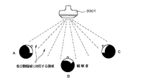
3001;複数画像同時表示装置
3002;CRT
3003;レンチキュラレンズ
4022;半透過型液晶表示パネル
4040;画素4040
4041R;透過領域(赤)
4042R;反射領域(赤)
4041G;透過領域(緑)
4042G;反射領域(緑)
4041B;透過領域(青)
4042B;反射領域(青)
5001;下側基板
5003;反射電極
5008;透明電極
5011;カラーフィルタ層
5011a;赤色カラーフィルタ層
5011b;緑色カラーフィルタ層
5011c;青色カラーフィルタ層
5021;信号電極
5022;走査電極
5023;薄膜トランジスタ(TFT)
また、レンチキュラレンズ31と観察者との間の距離を最適観察距離ODとし、この距離ODにおける画素の拡大投影像の周期、即ち、レンズから距離ODだけ離れレンズと平行な仮想平面上における左眼用画素43L及び右眼用画素43Rの投影像の幅の周期を夫々eとする。更に、レンチキュラレンズ31の中央に位置するシリンドリカルレンズ31aの中心から、X軸方向におけるレンチキュラレンズ31の端に位置するシリンドリカルレンズ31aの中心までの距離をWLとし、半透過型液晶表示パネル23の中心に位置する左眼用画素43Lと右眼用画素43Rからなる表示画素の中心と、X軸方向における半透過型液晶表示パネル23の端に位置する表示画素の中心との間の距離をWPとする。更にまた、レンチキュラレンズ31の中央に位置するシリンドリカルレンズ31aにおける光の入射角及び出射角を夫々α及びβとし、X軸方向におけるレンチキュラレンズ31の端に位置するシリンドリカルレンズ31aにおける光の入射角及び出射角を夫々γ及びδとする。更にまた、距離WLと距離WPとの差をCとし、距離WPの領域に含まれる画素数を2m個とする。なお、図15では、レンズのぼかし量が少なく左眼用画素43L及び右眼用画素43Rの投影像の幅がeとみなせる場合について描いてあるが、ぼかし量が大きくなるに従って各画素の投影像の幅が大きくなるものの、両側の投影像との重なりが大きくなるだけなので、周期はeのままである。本実施形態以降の第4実施形態乃至第9実施形態においても、同様に図では投影像の幅が周期と同等とみなせるように図示してあり、図では投影像の幅がeと読み取れるが、あくまでも投影像の幅の周期がeである。シリンドリカルレンズ31aの配列ピッチLと画素の配列ピッチPとは相互に関係しているため、一方に合わせて他方を決めることになるが、通常、表示パネルに合わせてレンチキュラレンズを設計することが多いため、画素の配列ピッチPを定数として扱う。また、レンチキュラレンズ31aの材料を選択することにより、屈折率nが決定される。これに対して、レンズと観察者との間の観察距離OD、及び観察距離ODにおける画素拡大投影像の周期eは所望の値を設定する。これらの値を使用して、レンズの頂点と画素との間の距離H及びレンズピッチLを決定する。スネルの法則と幾何学的関係より、下記数式1乃至6が成立する。また、下記数式7乃至9が成立する。

Claims (19)
- マトリクス状に配列され少なくとも第1視点用の画像を表示する画素及び第2視点用の画像を表示する画素を含む複数の表示単位と、前記表示単位内における前記第1視点用の画像を表示する画素と前記第2視点用の画像を表示する画素とが配列された第1の方向に沿って前記各画素から出射した光を相互に異なる方向に振り分ける光学部材と、前記各画素の少なくとも表示領域に夫々設けられたカラーフィルタ層と、前記各画素における前記カラーフィルタ層に設けられたスルーホールと、を有し、前記第1の方向と直交する方向を第2の方向とする場合、同一色の前記カラーフィルタ層を備えた前記第1視点用の画像を表示する画素と前記第2視点用の画像を表示する画素とが前記第1の方向に配列され、異なる色の前記カラーフィルタ層を備えた同一視点用の画像を表示する前記画素が前記第2の方向に配列され、前記表示単位に含まれる前記第1視点用の画像を表示する画素と前記第2視点用の画像を表示する画素における前記スルーホールの前記第1の方向における相対的な位置は同一であり、前記第2の方向に隣接する画素における前記スルーホールの前記第1の方向における相対的な位置は異なることを特徴とする表示パネル。
- 前記第1の方向に隣接する前記表示単位に含まれる画素における前記スルーホールの第1の方向における相対的な位置は、同一であることを特徴とする請求項1に記載の表示パネル。
- 前記第1の方向に隣接する前記表示単位に含まれる画素は、前記第2の方向に延伸する線分に対して線対称に配置されることを特徴とする請求項1に記載の表示パネル。
- 前記第1の方向に隣接する前記表示単位に含まれる画素は、回転対称に配置されることを特徴とする請求項1に記載の表示パネル。
- 前記同一視点用の画像を表示する複数画素において、前記第2の方向に延伸する線分に対して線対称の関係の画素が存在することを特徴とする請求項1乃至4のいずれか1項に記載の表示パネル。
- 前記表示パネルの画素が平行四辺形状を呈し、前記第2の方向に隣接する画素が前記第2の方向に延伸する線分に対して線対称の関係であることを特徴とする請求項5に記載の表示パネル。
- 前記同一視点用の画像を表示する複数画素において、前記第2の方向に延伸する線分に対して回転対称の関係の画素が存在することを特徴とする請求項1乃至4のいずれか1項に記載の表示パネル。
- 前記表示パネルの画素が台形状を呈することを特徴とする請求項7に記載の表示パネル。
- 前記第2の方向に隣接する画素に関し、前記各画素における前記スルーホールの相対的な位置及び形状が、前記第2の方向に延伸する線分に対して、線対称の関係にあることを特徴とする請求項8に記載の表示パネル。
- 前記第2の方向に隣接する各画素において各スルーホールの前記第1の方向の相対位置を保ちつつ重ね合わる場合、前記第2の方向におけるスルーホールの開口幅の合計値が、前記第1の方向によらず略一定となることを特徴とする請求項1乃至9のいずれか1項に記載の表示パネル。
- 前記光学部材は前記画素と結像関係にないことを特徴とする請求項1乃至10のいずれか1項に記載の表示パネル。
- 前記第2の方向における前記スルーホールの幅が、前記第1の方向に徐々に変化することを特徴とする請求項1乃至11のいずれか1項に記載の表示パネル。
- 前記スルーホールは前記各画素内において前記第1の方向に対して分断した形状をなすことを特徴とする請求項1乃至12のいずれか1項に記載の表示パネル。
- マトリクス状に配列され少なくとも第1視点用の画像を表示する画素及び第2視点用の画像を表示する画素を含む複数の表示単位と、前記表示単位内における前記第1視点用の画像を表示する画素と前記第2視点用の画像を表示する画素とを配列した第1の方向に沿って前記各画素から出射した光を相互に異なる方向に振り分ける光学部材と、前記各画素の表示領域に夫々設けられたカラーフィルタ層と、前記各画素における前記カラーフィルタ層に設けられたスルーホールと、を有し、前記各画素内において、前記スルーホールは前記第1の方向に対して分断した形状をなし、前記光学部材は前記画素と結像関係になく、前記光学部材は、少なくとも前記第1の方向にレンズが配列するように形成されたレンズアレイであり、前記レンズアレイのレンズピッチをLとし、このレンズの屈折率をnとし、観察距離ODにおける前記各画素の拡大投影像の周期をeとし、前記第1の方向における前記スルーホールの幅を各画素ピッチで除した値をtとし、このスルーホールの幅が各画素の幅の半分以上であるとき、前記レンズの曲率rが下記数式のいずれかを満たすことを特徴とする表示パネル。
r≦OD×(n−1)×L/(n×(1−t)×e+(n−1)×L)
r≧OD×(n−1)×L/(n×(1−t)×e−(n+1)×L) - マトリクス状に配列され少なくとも第1視点用の画像を表示する画素及び第2視点用の画像を表示する画素を含む複数の表示単位と、前記表示単位内における前記第1視点用の画像を表示する画素と前記第2視点用の画像を表示する画素とを配列した第1の方向に沿って前記各画素から出射した光を相互に異なる方向に振り分ける光学部材と、前記各画素の表示領域に夫々設けられたカラーフィルタ層と、前記各画素における前記カラーフィルタ層に設けられたスルーホールと、を有し、前記各画素内において、前記スルーホールは前記第1の方向に対して分断した形状をなし、前記光学部材は前記画素と結像関係になく、前記光学部材は、少なくとも前記第1の方向にレンズが配列するように形成されたレンズアレイであり、前記レンズアレイのレンズピッチをLとし、このレンズの屈折率をnとし、観察距離ODにおける前記各画素の拡大投影像の周期をeとし、前記第1の方向における前記スルーホールの幅を各画素ピッチで除した値をtとし、このスルーホールの幅が各画素の幅の半分未満であるとき、前記レンズの曲率rが下記数式のいずれかを満たすことを特徴とする表示パネル。
r≦OD×(n−1)×L/(n×t×e+(n−1)×L)
r≧OD×(n−1)×L/(n×t×e−(n+1)×L) - マトリクス状に配列され少なくとも第1視点用の画像を表示する画素及び第2視点用の画像を表示する画素を含む複数の表示単位と、前記表示単位内における前記第1視点用の画像を表示する画素と前記第2視点用の画像を表示する画素とを配列した第1の方向に沿って前記各画素から出射した光を相互に異なる方向に振り分ける光学部材と、前記各画素の表示領域に夫々設けられたカラーフィルタ層と、前記各画素における前記カラーフィルタ層に設けられたスルーホールと、を有し、前記各画素内において、前記スルーホールは前記第1の方向に対して分断した形状をなし、前記光学部材は前記画素と結像関係になく、前記光学部材は、少なくとも前記第1の方向に有限幅の開口が配列するように形成され、支持基板を有するパララックスバリアであり、前記パララックスバリアと前記画素との距離をHとし、前記支持基板の屈折率をnとし、観察距離ODにおける前記各画素の拡大投影像の周期をeとし、前記第1の方向における前記スルーホールの幅を各画素ピッチで除した値をtとし、このスルーホールの幅が各画素の幅の半分以上であるとき、前記パララックスバリアの開口の幅Sが下記数式を満たすことを特徴とする表示パネル。
S≧2×H×tan(1/n×arcsin(sin(arctan((1−t)×e/OD/2)))) - マトリクス状に配列され少なくとも第1視点用の画像を表示する画素及び第2視点用の画像を表示する画素を含む複数の表示単位と、前記表示単位内における前記第1視点用の画像を表示する画素と前記第2視点用の画像を表示する画素とを配列した第1の方向に沿って前記各画素から出射した光を相互に異なる方向に振り分ける光学部材と、前記各画素の表示領域に夫々設けられたカラーフィルタ層と、前記各画素における前記カラーフィルタ層に設けられたスルーホールと、を有し、前記各画素内において、前記スルーホールは前記第1の方向に対して分断した形状をなし、前記光学部材は前記画素と結像関係になく、前記光学部材は、少なくとも前記第1の方向に有限幅の開口が配列するように形成され、支持基板を有するパララックスバリアであり、前記パララックスバリアと前記画素との距離をHとし、前記支持基板の屈折率をnとし、観察距離ODにおける前記各画素の拡大投影像の周期をeとし、前記第1の方向における前記スルーホールの幅を各画素ピッチで除した値をtとし、このスルーホールの幅が各画素の幅の半分未満であるとき、前記パララックスバリアの開口の幅Sが下記数式を満たすことを特徴とする表示パネル。
S≧2×H×tan(1/n×arcsin(sin(arctan(t×e/OD/2)))) - 請求項1乃至17のいずれか1項に記載の表示パネルを有することを特徴とする表示装置。
- 請求項18に記載の表示装置を有することを特徴とする端末装置。
Priority Applications (1)
| Application Number | Priority Date | Filing Date | Title |
|---|---|---|---|
| JP2008522612A JP5472783B2 (ja) | 2006-06-27 | 2007-06-27 | 表示パネル、表示装置及び端末装置 |
Applications Claiming Priority (4)
| Application Number | Priority Date | Filing Date | Title |
|---|---|---|---|
| JP2006176331 | 2006-06-27 | ||
| JP2006176331 | 2006-06-27 | ||
| JP2008522612A JP5472783B2 (ja) | 2006-06-27 | 2007-06-27 | 表示パネル、表示装置及び端末装置 |
| PCT/JP2007/062948 WO2008001825A1 (en) | 2006-06-27 | 2007-06-27 | Display panel, display device, and terminal device |
Publications (2)
| Publication Number | Publication Date |
|---|---|
| JPWO2008001825A1 JPWO2008001825A1 (ja) | 2009-11-26 |
| JP5472783B2 true JP5472783B2 (ja) | 2014-04-16 |
Family
ID=38845590
Family Applications (1)
| Application Number | Title | Priority Date | Filing Date |
|---|---|---|---|
| JP2008522612A Active JP5472783B2 (ja) | 2006-06-27 | 2007-06-27 | 表示パネル、表示装置及び端末装置 |
Country Status (4)
| Country | Link |
|---|---|
| US (3) | US8760761B2 (ja) |
| JP (1) | JP5472783B2 (ja) |
| CN (2) | CN101479643B (ja) |
| WO (1) | WO2008001825A1 (ja) |
Families Citing this family (24)
| Publication number | Priority date | Publication date | Assignee | Title |
|---|---|---|---|---|
| WO2010007787A1 (ja) * | 2008-07-15 | 2010-01-21 | Yoshida Kenji | 裸眼立体映像表示システム、裸眼立体映像表示装置、遊技ゲーム機、パララックスバリアシート |
| JP5488984B2 (ja) * | 2009-04-15 | 2014-05-14 | Nltテクノロジー株式会社 | 表示コントローラ、表示装置、画像処理方法及び画像処理プログラム |
| US8797231B2 (en) * | 2009-04-15 | 2014-08-05 | Nlt Technologies, Ltd. | Display controller, display device, image processing method, and image processing program for a multiple viewpoint display |
| JP5380736B2 (ja) * | 2009-04-15 | 2014-01-08 | Nltテクノロジー株式会社 | 表示コントローラ、表示装置、画像処理方法及び画像処理プログラム |
| KR20110024970A (ko) * | 2009-09-03 | 2011-03-09 | 삼성전자주식회사 | 입체영상 표시 장치 |
| JP2012094310A (ja) * | 2010-10-26 | 2012-05-17 | Panasonic Corp | 照明装置 |
| US9218115B2 (en) | 2010-12-02 | 2015-12-22 | Lg Electronics Inc. | Input device and image display apparatus including the same |
| JP5732888B2 (ja) * | 2011-02-14 | 2015-06-10 | ソニー株式会社 | 表示装置及び表示方法 |
| US9420268B2 (en) | 2011-06-23 | 2016-08-16 | Lg Electronics Inc. | Apparatus and method for displaying 3-dimensional image |
| CN103135279B (zh) * | 2011-12-05 | 2015-09-09 | 上海中航光电子有限公司 | 一种薄膜晶体管液晶显示装置 |
| JP6358494B2 (ja) * | 2013-02-27 | 2018-07-18 | Tianma Japan株式会社 | 立体画像表示装置 |
| CN104765158B (zh) * | 2015-05-06 | 2017-08-29 | 合肥京东方光电科技有限公司 | 视差挡板及显示装置 |
| CN106959551B (zh) * | 2016-01-08 | 2023-12-19 | 京东方科技集团股份有限公司 | 一种显示装置及其驱动方法 |
| CN105789261B (zh) * | 2016-04-29 | 2018-03-06 | 京东方科技集团股份有限公司 | 像素阵列及其制造方法和有机发光二极管阵列基板 |
| TWI634350B (zh) * | 2016-08-10 | 2018-09-01 | 群睿股份有限公司 | 影像顯示方法 |
| CN107765438B (zh) * | 2016-08-18 | 2020-09-15 | 群睿股份有限公司 | 影像显示装置及影像显示方法 |
| CN108139591B (zh) * | 2016-09-20 | 2020-08-14 | 京东方科技集团股份有限公司 | 三维显示面板、包括其的三维显示设备、及其制造方法 |
| US10732743B2 (en) | 2017-07-18 | 2020-08-04 | Apple Inc. | Concealable input region for an electronic device having microperforations |
| CN108594517B (zh) * | 2018-05-04 | 2021-04-06 | 京东方科技集团股份有限公司 | 一种液晶显示装置及其控制方法 |
| US11036321B2 (en) * | 2018-07-27 | 2021-06-15 | Lg Display Co., Ltd. | Light control film and display apparatus including the same |
| CN109298536B (zh) * | 2018-11-20 | 2023-09-12 | 成都航空职业技术学院 | 一种一维双视3d显示装置 |
| JP7394691B2 (ja) * | 2020-04-07 | 2023-12-08 | 株式会社Imagica Group | 立体表示装置 |
| CN113752833B (zh) * | 2021-09-14 | 2022-03-04 | 黑龙江天有为电子有限责任公司 | 一种汽车仪表盘 |
| CN113625464A (zh) * | 2021-09-17 | 2021-11-09 | 纵深视觉科技(南京)有限责任公司 | 一种立体显示设备 |
Citations (6)
| Publication number | Priority date | Publication date | Assignee | Title |
|---|---|---|---|---|
| JP2002333622A (ja) * | 2001-03-07 | 2002-11-22 | Sharp Corp | 反射透過両用型カラー液晶表示装置 |
| JP2003233063A (ja) * | 2002-02-12 | 2003-08-22 | Matsushita Electric Ind Co Ltd | 液晶表示装置 |
| JP2004184969A (ja) * | 2002-10-11 | 2004-07-02 | Seiko Epson Corp | 電気光学装置の製造方法、電気光学装置及び電子機器 |
| JP2004280052A (ja) * | 2003-02-28 | 2004-10-07 | Nec Corp | 画像表示装置、携帯端末装置、表示パネル及び画像表示方法 |
| JP2005031215A (ja) * | 2003-07-09 | 2005-02-03 | Hitachi Displays Ltd | 液晶表示装置 |
| JP2005208567A (ja) * | 2003-12-25 | 2005-08-04 | Nec Corp | 画像表示装置、携帯端末装置、表示パネル及びレンズ |
Family Cites Families (10)
| Publication number | Priority date | Publication date | Assignee | Title |
|---|---|---|---|---|
| US5825466A (en) * | 1996-01-18 | 1998-10-20 | Image Technology International, Inc. | 3D photo printer with image distortion correction |
| JPH06332354A (ja) | 1993-05-20 | 1994-12-02 | Toppan Printing Co Ltd | 複数画像同時表示ディスプレイ |
| JP3335130B2 (ja) | 1998-01-26 | 2002-10-15 | シャープ株式会社 | 液晶表示装置 |
| KR100389249B1 (ko) * | 2000-04-29 | 2003-06-25 | 한국과학기술연구원 | 다시점 영상 표시 시스템 |
| US6501521B2 (en) | 2001-03-07 | 2002-12-31 | Sharp Kabushiki Kaisha | Transmission/reflection type color liquid crystal display device |
| JP2003066938A (ja) * | 2001-08-24 | 2003-03-05 | Sharp Corp | 表示コントローラ、表示制御方法、および画像表示システム |
| JP4075802B2 (ja) * | 2002-04-04 | 2008-04-16 | ソニー株式会社 | 液晶表示装置 |
| KR20050105570A (ko) * | 2004-04-30 | 2005-11-04 | 엘지.필립스 엘시디 주식회사 | 패턴드 스페이서를 구비한 액정표시장치용 컬러필터 기판및 그 제조방법 |
| CN100487782C (zh) * | 2004-08-18 | 2009-05-13 | 奇景光电股份有限公司 | 彩色序列式显示器的显示方法 |
| US7965365B2 (en) * | 2004-09-03 | 2011-06-21 | Nec Lcd Technologies, Ltd | Image display device, portable terminal, display panel, and lens |
-
2007
- 2007-06-27 WO PCT/JP2007/062948 patent/WO2008001825A1/ja active Application Filing
- 2007-06-27 US US12/306,763 patent/US8760761B2/en active Active
- 2007-06-27 JP JP2008522612A patent/JP5472783B2/ja active Active
- 2007-06-27 CN CN2007800244907A patent/CN101479643B/zh active Active
- 2007-06-27 CN CN201310129476.0A patent/CN103257452B/zh active Active
-
2014
- 2014-05-12 US US14/275,330 patent/US9360677B2/en active Active
-
2016
- 2016-05-17 US US15/156,876 patent/US10317688B2/en active Active
Patent Citations (6)
| Publication number | Priority date | Publication date | Assignee | Title |
|---|---|---|---|---|
| JP2002333622A (ja) * | 2001-03-07 | 2002-11-22 | Sharp Corp | 反射透過両用型カラー液晶表示装置 |
| JP2003233063A (ja) * | 2002-02-12 | 2003-08-22 | Matsushita Electric Ind Co Ltd | 液晶表示装置 |
| JP2004184969A (ja) * | 2002-10-11 | 2004-07-02 | Seiko Epson Corp | 電気光学装置の製造方法、電気光学装置及び電子機器 |
| JP2004280052A (ja) * | 2003-02-28 | 2004-10-07 | Nec Corp | 画像表示装置、携帯端末装置、表示パネル及び画像表示方法 |
| JP2005031215A (ja) * | 2003-07-09 | 2005-02-03 | Hitachi Displays Ltd | 液晶表示装置 |
| JP2005208567A (ja) * | 2003-12-25 | 2005-08-04 | Nec Corp | 画像表示装置、携帯端末装置、表示パネル及びレンズ |
Also Published As
| Publication number | Publication date |
|---|---|
| US10317688B2 (en) | 2019-06-11 |
| US20140240826A1 (en) | 2014-08-28 |
| CN101479643A (zh) | 2009-07-08 |
| WO2008001825A1 (en) | 2008-01-03 |
| US9360677B2 (en) | 2016-06-07 |
| US20160259173A1 (en) | 2016-09-08 |
| US8760761B2 (en) | 2014-06-24 |
| CN101479643B (zh) | 2013-08-28 |
| CN103257452B (zh) | 2016-08-03 |
| JPWO2008001825A1 (ja) | 2009-11-26 |
| US20090257119A1 (en) | 2009-10-15 |
| CN103257452A (zh) | 2013-08-21 |
Similar Documents
| Publication | Publication Date | Title |
|---|---|---|
| JP5472783B2 (ja) | 表示パネル、表示装置及び端末装置 | |
| JP4371012B2 (ja) | 画像表示装置、携帯端末装置、表示パネル及びレンズ | |
| CN102269893B (zh) | 显示设备、终端设备、显示面板和光学构件 | |
| JP4492851B2 (ja) | 視差バリアおよび複数表示ディスプレイ | |
| US8248406B2 (en) | Image display device, portable terminal device, display panel and image display method using the same | |
| JP4947526B2 (ja) | 画像表示装置 | |
| CN102749714B (zh) | 图像显示装置、显示面板和终端装置 | |
| JP5544646B2 (ja) | 表示装置及び端末装置 | |
| US7995166B2 (en) | Display panel, display device, and terminal device | |
| JP4196889B2 (ja) | 画像表示装置及び携帯端末装置 | |
| JP5224236B2 (ja) | 表示パネル、表示装置及び端末装置 | |
| JP5024800B2 (ja) | 画像表示装置 | |
| JP3925500B2 (ja) | 画像表示装置及びそれを使用した携帯端末装置 | |
| JP2004280078A (ja) | 画像表示装置、携帯端末装置及び表示パネル | |
| JP2007148420A (ja) | 画像表示装置及びそれを使用した携帯端末装置 | |
| JP2009015337A (ja) | 画像表示装置及び携帯端末装置 |
Legal Events
| Date | Code | Title | Description |
|---|---|---|---|
| A621 | Written request for application examination |
Free format text: JAPANESE INTERMEDIATE CODE: A621 Effective date: 20100517 |
|
| A131 | Notification of reasons for refusal |
Free format text: JAPANESE INTERMEDIATE CODE: A131 Effective date: 20130305 |
|
| A521 | Request for written amendment filed |
Free format text: JAPANESE INTERMEDIATE CODE: A523 Effective date: 20130430 |
|
| TRDD | Decision of grant or rejection written | ||
| A01 | Written decision to grant a patent or to grant a registration (utility model) |
Free format text: JAPANESE INTERMEDIATE CODE: A01 Effective date: 20140107 |
|
| A61 | First payment of annual fees (during grant procedure) |
Free format text: JAPANESE INTERMEDIATE CODE: A61 Effective date: 20140123 |
|
| R150 | Certificate of patent or registration of utility model |
Ref document number: 5472783 Country of ref document: JP Free format text: JAPANESE INTERMEDIATE CODE: R150 Free format text: JAPANESE INTERMEDIATE CODE: R150 |
|
| R250 | Receipt of annual fees |
Free format text: JAPANESE INTERMEDIATE CODE: R250 |
|
| R250 | Receipt of annual fees |
Free format text: JAPANESE INTERMEDIATE CODE: R250 |
|
| R250 | Receipt of annual fees |
Free format text: JAPANESE INTERMEDIATE CODE: R250 |
|
| R250 | Receipt of annual fees |
Free format text: JAPANESE INTERMEDIATE CODE: R250 |
|
| R250 | Receipt of annual fees |
Free format text: JAPANESE INTERMEDIATE CODE: R250 |
|
| R250 | Receipt of annual fees |
Free format text: JAPANESE INTERMEDIATE CODE: R250 |
|
| R250 | Receipt of annual fees |
Free format text: JAPANESE INTERMEDIATE CODE: R250 |
|
| R250 | Receipt of annual fees |
Free format text: JAPANESE INTERMEDIATE CODE: R250 |
|
| R250 | Receipt of annual fees |
Free format text: JAPANESE INTERMEDIATE CODE: R250 |