JP5436404B2 - Semiconductor pressure sensor and manufacturing method thereof - Google Patents
Semiconductor pressure sensor and manufacturing method thereof Download PDFInfo
- Publication number
- JP5436404B2 JP5436404B2 JP2010281549A JP2010281549A JP5436404B2 JP 5436404 B2 JP5436404 B2 JP 5436404B2 JP 2010281549 A JP2010281549 A JP 2010281549A JP 2010281549 A JP2010281549 A JP 2010281549A JP 5436404 B2 JP5436404 B2 JP 5436404B2
- Authority
- JP
- Japan
- Prior art keywords
- pressure sensor
- semiconductor pressure
- insulating film
- polysilicon
- manufacturing
- Prior art date
- Legal status (The legal status is an assumption and is not a legal conclusion. Google has not performed a legal analysis and makes no representation as to the accuracy of the status listed.)
- Expired - Fee Related
Links
- 239000004065 semiconductor Substances 0.000 title claims description 188
- 238000004519 manufacturing process Methods 0.000 title claims description 70
- 229910021420 polycrystalline silicon Inorganic materials 0.000 claims description 207
- 229920005591 polysilicon Polymers 0.000 claims description 207
- 238000005530 etching Methods 0.000 claims description 104
- 239000000758 substrate Substances 0.000 claims description 78
- 229910052751 metal Inorganic materials 0.000 claims description 48
- 239000002184 metal Substances 0.000 claims description 48
- 239000013078 crystal Substances 0.000 claims description 15
- 238000000034 method Methods 0.000 claims description 15
- 239000011521 glass Substances 0.000 claims description 13
- 230000002093 peripheral effect Effects 0.000 claims description 3
- 238000003475 lamination Methods 0.000 claims 1
- 239000010408 film Substances 0.000 description 142
- XUIMIQQOPSSXEZ-UHFFFAOYSA-N Silicon Chemical compound [Si] XUIMIQQOPSSXEZ-UHFFFAOYSA-N 0.000 description 55
- 229910052710 silicon Inorganic materials 0.000 description 55
- 239000010703 silicon Substances 0.000 description 55
- 238000007789 sealing Methods 0.000 description 13
- 238000000059 patterning Methods 0.000 description 12
- 238000005229 chemical vapour deposition Methods 0.000 description 11
- BOTDANWDWHJENH-UHFFFAOYSA-N Tetraethyl orthosilicate Chemical compound CCO[Si](OCC)(OCC)OCC BOTDANWDWHJENH-UHFFFAOYSA-N 0.000 description 9
- 230000000694 effects Effects 0.000 description 9
- 238000010586 diagram Methods 0.000 description 8
- 239000012535 impurity Substances 0.000 description 7
- WGTYBPLFGIVFAS-UHFFFAOYSA-M tetramethylammonium hydroxide Chemical compound [OH-].C[N+](C)(C)C WGTYBPLFGIVFAS-UHFFFAOYSA-M 0.000 description 6
- 230000006870 function Effects 0.000 description 4
- XLYOFNOQVPJJNP-UHFFFAOYSA-N water Substances O XLYOFNOQVPJJNP-UHFFFAOYSA-N 0.000 description 4
- ZOXJGFHDIHLPTG-UHFFFAOYSA-N Boron Chemical compound [B] ZOXJGFHDIHLPTG-UHFFFAOYSA-N 0.000 description 3
- 238000000137 annealing Methods 0.000 description 3
- 229910052796 boron Inorganic materials 0.000 description 3
- 230000015572 biosynthetic process Effects 0.000 description 2
- 238000004140 cleaning Methods 0.000 description 2
- 238000000151 deposition Methods 0.000 description 2
- 239000007788 liquid Substances 0.000 description 2
- 239000000463 material Substances 0.000 description 2
- 230000002265 prevention Effects 0.000 description 2
- 230000035945 sensitivity Effects 0.000 description 2
- 239000010409 thin film Substances 0.000 description 2
- OAICVXFJPJFONN-UHFFFAOYSA-N Phosphorus Chemical compound [P] OAICVXFJPJFONN-UHFFFAOYSA-N 0.000 description 1
- 229910052782 aluminium Inorganic materials 0.000 description 1
- XAGFODPZIPBFFR-UHFFFAOYSA-N aluminium Chemical compound [Al] XAGFODPZIPBFFR-UHFFFAOYSA-N 0.000 description 1
- 238000004891 communication Methods 0.000 description 1
- 239000000470 constituent Substances 0.000 description 1
- 238000009792 diffusion process Methods 0.000 description 1
- 239000006185 dispersion Substances 0.000 description 1
- 238000001035 drying Methods 0.000 description 1
- 238000010438 heat treatment Methods 0.000 description 1
- 150000002739 metals Chemical class 0.000 description 1
- 229910052698 phosphorus Inorganic materials 0.000 description 1
- 239000011574 phosphorus Substances 0.000 description 1
- 238000005268 plasma chemical vapour deposition Methods 0.000 description 1
- 238000005498 polishing Methods 0.000 description 1
- 230000009993 protective function Effects 0.000 description 1
- 238000004544 sputter deposition Methods 0.000 description 1
- 238000007740 vapor deposition Methods 0.000 description 1
- 238000005406 washing Methods 0.000 description 1
Images


Classifications
-
- G—PHYSICS
- G01—MEASURING; TESTING
- G01L—MEASURING FORCE, STRESS, TORQUE, WORK, MECHANICAL POWER, MECHANICAL EFFICIENCY, OR FLUID PRESSURE
- G01L9/00—Measuring steady of quasi-steady pressure of fluid or fluent solid material by electric or magnetic pressure-sensitive elements; Transmitting or indicating the displacement of mechanical pressure-sensitive elements, used to measure the steady or quasi-steady pressure of a fluid or fluent solid material, by electric or magnetic means
- G01L9/0041—Transmitting or indicating the displacement of flexible diaphragms
- G01L9/0051—Transmitting or indicating the displacement of flexible diaphragms using variations in ohmic resistance
- G01L9/0052—Transmitting or indicating the displacement of flexible diaphragms using variations in ohmic resistance of piezoresistive elements
- G01L9/0054—Transmitting or indicating the displacement of flexible diaphragms using variations in ohmic resistance of piezoresistive elements integral with a semiconducting diaphragm
-
- Y—GENERAL TAGGING OF NEW TECHNOLOGICAL DEVELOPMENTS; GENERAL TAGGING OF CROSS-SECTIONAL TECHNOLOGIES SPANNING OVER SEVERAL SECTIONS OF THE IPC; TECHNICAL SUBJECTS COVERED BY FORMER USPC CROSS-REFERENCE ART COLLECTIONS [XRACs] AND DIGESTS
- Y10—TECHNICAL SUBJECTS COVERED BY FORMER USPC
- Y10T—TECHNICAL SUBJECTS COVERED BY FORMER US CLASSIFICATION
- Y10T29/00—Metal working
- Y10T29/49—Method of mechanical manufacture
Landscapes
- Physics & Mathematics (AREA)
- General Physics & Mathematics (AREA)
- Measuring Fluid Pressure (AREA)
- Pressure Sensors (AREA)
- Micromachines (AREA)
Description
本発明は、半導体圧力センサ及びその製造方法に関し、特に、ポリシリコンゲージ抵抗を備える半導体圧力センサ及びその製造方法に関するものである。 The present invention relates to a semiconductor pressure sensor and a manufacturing method thereof, and more particularly to a semiconductor pressure sensor having a polysilicon gauge resistor and a manufacturing method thereof.
圧力センサの一形態として、半導体基板を利用した半導体圧力センサが存在している。この半導体圧力センサでは、印加された圧力に応じて抵抗が変化するゲージ抵抗となる拡散抵抗が、シリコン基板の表面上に複数形成されており、この拡散抵抗が抵抗値の低い拡散配線によってブリッジ結線されている。ゲージ抵抗は、例えば、矩形状のダイヤフラム(薄膜)の4辺のそれぞれの部分に配置される。一方、シリコン基板において、ゲージが配置される領域の反対側の面には、ダイヤフラムを形成するための凹部が形成される。特許文献1には、この種の半導体圧力センサが開示されている。
As one form of pressure sensor, there is a semiconductor pressure sensor using a semiconductor substrate. In this semiconductor pressure sensor, a plurality of diffused resistors, which are gauge resistors whose resistance changes according to the applied pressure, are formed on the surface of the silicon substrate, and these diffused resistors are bridged by diffusion wires having a low resistance value. Has been. For example, the gauge resistance is arranged in each part of four sides of a rectangular diaphragm (thin film). On the other hand, in the silicon substrate, a recess for forming a diaphragm is formed on the surface opposite to the region where the gauge is disposed.
従来の半導体圧力センサにおいては、シリコン基板を所定の厚みにまで研磨した後、さらに所定のエッチングマスクを介してシリコン基板の裏面にエッチングを施すことによって、上述の凹部、つまりダイヤフラムが形成される。 In the conventional semiconductor pressure sensor, after the silicon substrate is polished to a predetermined thickness, the back surface of the silicon substrate is further etched through a predetermined etching mask, thereby forming the above-described recess, that is, the diaphragm.
このような製造方法では、凹部下のシリコン基板の厚みが、エッチングの時間によって制御されることから、ダイヤフラムの厚みがばらつきやすいという問題があった。また、ダイヤフラムの厚みを薄くしようとしても、シリコン基板の研磨量とエッチング量のシリコン基板面内におけるばらつき量を考慮すると、その厚みは10μm程度が限界であった。また、シリコン基板のエッチングのばらつきにより、ゲージ抵抗に対して凹部の位置がずれてしまうことから高精度に小型化することが困難であった。 In such a manufacturing method, since the thickness of the silicon substrate under the recess is controlled by the etching time, there is a problem that the thickness of the diaphragm is likely to vary. Even if the thickness of the diaphragm is reduced, the thickness is limited to about 10 μm in consideration of the amount of polishing of the silicon substrate and the variation in the etching amount in the silicon substrate surface. In addition, due to variations in etching of the silicon substrate, the position of the concave portion is shifted with respect to the gauge resistance, so that it is difficult to reduce the size with high accuracy.
そこで、本発明は、上記のような問題点を鑑みてなされたものであり、半導体圧力センサの小型化に伴う性能のばらつきを抑制することが可能な技術を提供することを目的とする。 Therefore, the present invention has been made in view of the above-described problems, and an object thereof is to provide a technique capable of suppressing performance variations accompanying downsizing of a semiconductor pressure sensor.
本発明に係る半導体圧力センサの製造方法は、(a)半導体基板上に複数の第1開口を有する第1絶縁膜を形成する工程と、(b)前記第1絶縁膜上に、当該第1絶縁膜の前記複数の第1開口内において前記半導体基板と接する犠牲層を形成する工程とを備える。そして、(c)ポリシリコンダイヤフラムと、当該ポリシリコンダイヤフラムの下方の真空室となるべき空間側に形成されたポリシリコンゲージ抵抗と、これらを内包し、前記犠牲層と接するエッチング液導入孔を有する絶縁膜群とを含む積層構造を、前記犠牲層上に形成する工程を備える。そして、(d)エッチング液を前記エッチング液導入孔に通じて、前記犠牲層をエッチングすることにより前記積層構造を前記真空室上で機能するダイヤフラム体として形成するとともに、前記半導体基板における前記第1絶縁膜の前記第1開口下の表面をエッチングすることにより前記真空室となるべき前記空間と、当該空間中に配置され、前記ダイヤフラム体の中央付近に向かって突出するダイヤフラムストッパーとを形成する工程を備える。 The method for manufacturing a semiconductor pressure sensor according to the present invention includes: (a) a step of forming a first insulating film having a plurality of first openings on a semiconductor substrate; and (b) the first insulating film on the first insulating film. Forming a sacrificial layer in contact with the semiconductor substrate in the plurality of first openings of the insulating film. And (c) a polysilicon diaphragm, a polysilicon gauge resistor formed on the space side to be a vacuum chamber below the polysilicon diaphragm, and an etchant introduction hole that includes these and contacts the sacrificial layer Forming a laminated structure including an insulating film group on the sacrificial layer. And (d) etching the sacrificial layer by passing an etching solution through the etching solution introduction hole to form the laminated structure as a diaphragm functioning on the vacuum chamber, and the first in the semiconductor substrate. Etching the surface under the first opening of the insulating film to form the space to be the vacuum chamber, and a diaphragm stopper disposed in the space and projecting toward the vicinity of the center of the diaphragm body Is provided.
本発明によれば、高精度に膜厚、形状及び位置合わせを制御することが可能な積層構造からダイヤフラム体を形成する。したがって、半導体圧力センサの小型化に伴う性能のばらつきを抑制することができる。また、ダイヤフラムストッパーが、ダイヤフラム体において歪み易い中央付近を支持するように突出していることから、ダイヤフラム体の破壊を防止することができ、ダイヤフラム体の薄膜化、小型化が期待できる。また、ポリシリコンゲージ抵抗は、ポリシリコンダイヤフラムの下方の真空室側に配置されていることから、外部環境の影響を受けにくくなる。よって、信頼性の高い半導体圧力センサを得ることができる。また、エッチングにより、ダイヤフラム体での空間が犠牲層に隣接して形成されていく。したがって、エッチング液等の流れを良くすることができることから、エッチング等の工程にかかる時間を短縮することができ、半導体圧力センサの製造時間を短縮することができる。 According to the present invention, the diaphragm body is formed from a laminated structure capable of controlling the film thickness, shape, and alignment with high accuracy. Therefore, it is possible to suppress variation in performance associated with downsizing of the semiconductor pressure sensor. In addition, since the diaphragm stopper protrudes so as to support the vicinity of the center that is easily distorted in the diaphragm body, it is possible to prevent the diaphragm body from being broken, and it can be expected that the diaphragm body is made thinner and smaller. Further, since the polysilicon gauge resistance is disposed on the vacuum chamber side below the polysilicon diaphragm, it is less susceptible to the influence of the external environment. Therefore, a highly reliable semiconductor pressure sensor can be obtained. Further, the space in the diaphragm body is formed adjacent to the sacrificial layer by etching. Therefore, since the flow of the etching solution or the like can be improved, the time required for the etching process or the like can be shortened, and the manufacturing time of the semiconductor pressure sensor can be shortened.
<実施の形態1>
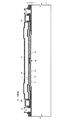
図1は本発明の実施の形態1に係る半導体圧力センサを示す平面図であり、図2は、図1に示されたA−A線における断面図である。
<
1 is a plan view showing a semiconductor pressure sensor according to
本実施の形態に係る半導体圧力センサは、複数(ここでは4つ)の凹部1aが表面に形成された半導体基板であるシリコン基板1と、シリコン基板1上に形成され複数の第1開口2aを有する第1絶縁膜2と、積層構造からなるダイヤフラム体11と、第1金属層21(図1においては細い破線)と、第2金属層22(図1においては太い破線)と、ガラスコート23(図1においては細い一点鎖線)とを備える。
The semiconductor pressure sensor according to the present embodiment includes a
ダイヤフラム体11は、ポリシリコン配線4a及びポリシリコンゲージ抵抗4bと、これらの上側に形成されたポリシリコンダイヤフラム6と、これらを内包する第2絶縁膜3、第3絶縁膜5及び第4絶縁膜7とからなる絶縁膜群とを含んでいる。ダイヤフラム体11は、凹部1a上の空間13を介してシリコン基板1の上側に形成されており、ダイヤフラム体11の周縁部は第1絶縁膜2に支持されている。このダイヤフラム体11は、シリコン基板1の表面側から裏面側に向かう方向(空間13に向かう方向)に、気圧などの圧力を受けると、その圧力に応じて下側に湾曲するように歪むようになっており、その歪み具合、つまり、圧力の大きさを示す電気信号を出力可能となっている。
The
空間13は真空室となっており、複数の凹部1aの外側に位置する封止部22aによって封止されている。以下の説明においては、空間13を「真空室13」と呼ぶこともある。本実施の形態では、シリコン基板1の複数の凹部1aと、第1絶縁膜2の複数の第1開口2aと、ダイヤフラム体11の凹部1a側の表面とが、この真空室13(空間13)を形成している。そして、真空室13と連通するエッチング液導入孔15が、平面視(図1)においてダイヤフラム体11の外側の位置における絶縁膜群に設けられており、封止部22aによって封止されている。
The
次に、本実施の形態に係る半導体圧力センサの構成要素について詳細に説明する。 Next, components of the semiconductor pressure sensor according to the present embodiment will be described in detail.
平面視(図1)において4つの凹部1aのそれぞれは、シリコン基板1表面に矩形状を有しており、縦及び横方向に2つずつ互いに離間させて配列されている。この凹部1aは、断面視(図2)においては下側に先細りの凸形状を有している。2つの凹部1a同士の間のシリコン基板1表面の高さは、第1絶縁膜2が形成されたシリコン基板1表面の高さと同じとなっており、シリコン基板1は、ダイヤフラム体11に向かう先細りの凸部1bを有している。凸部1bの先端には、絶縁膜をパターニングして第1絶縁膜2と同時に形成された先端絶縁膜2bが設けられている。
In plan view (FIG. 1), each of the four
真空室13におけるシリコン基板1には、ダイヤフラム体11の中央付近に向かって突出するダイヤフラムストッパー12が配置されている。本実施の形態では、このダイヤフラムストッパー12は、凸部1b及び先端絶縁膜2bから構成されており、ダイヤフラム体11が外部から大きな圧力を受けて破壊されるのを防ぐ機能を有するとともに、製造時にダイヤフラム体11の第2絶縁膜2がシリコン基板1と固着するのを防ぐ機能を有する。
A
本実施の形態では、ダイヤフラムストッパー12の先端部(ここでは先端絶縁膜2b)は、平面視(図1)において、4つの凹部1aの隙間に存在する十字型の形状を有している。そして、ダイヤフラムストッパー12の先端部(ここでは先端絶縁膜2b)の幅は5μm以下となっている。
In the present embodiment, the distal end portion (here, the distal
第1絶縁膜2は、シリコン基板1上に形成されており、複数の凹部1aにそれぞれ対応した複数の第1第1開口2aを有する。つまり、平面視(図1)において、複数の第1開口2aのそれぞれは、凹部1aと同様に、矩形状を有し、縦及び横方向に2つずつ配列されている。第1絶縁膜2は、例えば、HTOやTEOSなどの酸化膜をCVD(Chemical Vapor Deposition)などにより形成した後パターニングして形成される。
The first
第2絶縁膜3は、図2に示されるように、互いに対向する封止部22aの外側では、概ね、第1絶縁膜2上に形成されているが、封止部22aの内側では、概ね、空隙14を介して第1絶縁膜2上方に形成されている。ただし、平面視(図1)に示されるアンカー17では、封止部22aの内側であっても第2絶縁膜3と第1絶縁膜2とが互いに接するように形成されている。つまり、第2絶縁膜2は、ダイヤフラム体11の周縁部(アンカー17)において第1絶縁膜2に支持されている。第2絶縁膜3は、例えば、HTOやTEOSなどの酸化膜をCVDにより形成した後パターニングして形成される。
As shown in FIG. 2, the second
断面視(図2)において、ポリシリコン配線4a及びポリシリコンゲージ抵抗4bは第2絶縁膜3上に形成されている。平面視(図1)においてポリシリコン配線4aは、上述のダイヤフラムストッパー12の先端部の十字型とほぼ同じ形状によって4つに区分されており、縦及び横方向に隣接するポリシリコン配線4a同士は、それぞれ、ポリシリコンゲージ抵抗4bを介して接続されている。4つのポリシリコン配線4aの全体の形状は、4隅のそれぞれにおいて外側に少し張り出した張出部4aaを有する略矩形状となっている。
In a cross-sectional view (FIG. 2), the
平面視(図1)において4つのポリシコンゲージ抵抗4bのそれぞれは、左右方向に延在するように形成されており、これらは互いに同サイズに形成される。本実施の形態では、横方向に隣接するポリシリコン配線4aを接続する2つのポリシリコンゲージ抵抗4baは、ダイヤフラム体11の中央付近において形成されており、縦方向に隣接するポリシリコン配線4aを接続する2つのポリシリコンゲージ抵抗4bbは、ダイヤフラム体11の互いに対向する二つのエッジ付近にそれぞれ形成されている。そして、4つのポリシリコンゲージ抵抗4bは、後述するホイートストンブリッジ回路を形成するように、ポリシリコン配線4aによってブリッジ結線されている。これらポリシリコンゲージ抵抗4bは、ピエゾ抵抗効果及び抵抗値が最適値となるように、ポリシリコンにB(ボロン)やP(リン)などの不純物注入が行われた後、アニールが行われて形成される。なお、本実施の形態では、ポリシリコンゲージ抵抗4bは、Bが注入されたp型のゲージ抵抗であるものとする。
In a plan view (FIG. 1), each of the four
断面視(図2)において第3絶縁膜5は、ポリシリコン配線4a及びポリシリコンゲージ抵抗4b上、及びこれらの側面に形成されている。この第3絶縁膜5は、図1に示されるポリシリコン配線4aの張出部4aa上においてポリシリコン配線4aを露出する開口たるポリシリコン配線コンタクト部分5aを複数有する。このポリシリコン配線コンタクト部分5a内のポリシリコン配線4a上には第1金属層21(細い破線)が形成されている。なお、第3絶縁膜5は、例えば、HTOやTEOSなどの酸化膜をCVDにより形成した後パターニングして形成される。
In a sectional view (FIG. 2), the third
断面視(図2)においてポリシリコンダイヤフラム6は、第3絶縁膜5上に形成される。このポリシリコンダイヤフラムは、例えばドープドポリシリコンで形成されている。
In a cross-sectional view (FIG. 2), the
断面視(図2)において第4絶縁膜7は、ポリシリコンダイヤフラム6上及びその側面に形成されている。この第4絶縁膜7は、例えば、HTOやTEOSなどの酸化膜をCVDにより形成した後パターニングして形成される。
In a cross-sectional view (FIG. 2), the fourth insulating
第2絶縁膜3、第3絶縁膜5及び第4絶縁膜7(絶縁膜群)には、図2に示されるように、空隙14を介して空間13と連通するエッチング液導入孔15が設けられている。このエッチング液導入孔15内には、第2金属層22の一部が封止部22aとして充填されている。
As shown in FIG. 2, the second
第2金属層22は、ポリシリコン配線コンタクト部分5a上と、当該ポリシリコン配線コンタクト部分5aと平面視(図1)において縦方向に隣接するエッチング液導入孔15上と、当該ポリシリコン配線コンタクト部分5aと平面視(図1)において横方向に隣接するエッチング液導入孔15上とに亘って形成されている。この第2金属層22は、ポリシリコン配線コンタクト部分5a内に形成された第1金属層21と接することによりポリシリコンゲージ抵抗4bをブリッジ結線する。また、第2金属層22は、上述したようにエッチング液導入孔15に充填されることにより空間13を真空封止する。この第2金属層22の材質には、例えば、Al(アルミニウム)が用いられる。
The
第2金属層22上には、第2金属層22を保護するガラスコート23が形成されている。なお、ガラスコート23は、ポリシリコンダイヤフラム6の形状と等しい開口を有するとともに、ポリシリコン配線コンタクト部分5a及びエッチング液導入孔15に関し、ポリシリコンダイヤフラム6と反対側において、第2金属層22を露出する開口23aを有している。この開口23a内の第2金属層22は、電極パッド22bとして用いられる。
A
次に、以上の構成からなる本実施の形態に係る半導体圧力センサの動作について説明する。この半導体圧力センサにおいて、ダイヤフラム体11に圧力が印加されると、ダイヤフラム体11がその圧力に応じて歪み、ダイヤフラム体11に含まれるポリシリコンゲージ抵抗4bの抵抗値が、その歪みに応じて変化する。
Next, the operation of the semiconductor pressure sensor according to the present embodiment having the above configuration will be described. In this semiconductor pressure sensor, when a pressure is applied to the
図3は、上述の4つのポリシリコンゲージ抵抗4bが、ポリシリコン配線4aによってブリッジ結線されている様子を示す図である。ここでは、図1に示したダイヤフラム体11中央側の二つのポリシリコンゲージ抵抗4baは抵抗R1,R3を有するものとし、ダイヤフラム体11エッジ側の二つのポリシリコンゲージ抵抗4bbは抵抗R2,R4を有するものとする。
FIG. 3 is a diagram showing a state where the four
図3においては、抵抗R1〜R4のポリシリコンゲージ抵抗4ba,4bbはホイートストンブリッジ回路を構成しており、抵抗R1及び抵抗R2のポリシリコンゲージ抵抗4ba,4bbの接点と、抵抗R3及び抵抗R4のポリシリコンゲージ抵抗4ba,4bbの接点との間には、入力電圧Vin(=5V)が印加されている。 In FIG. 3, the polysilicon gauge resistors 4ba and 4bb of the resistors R1 to R4 constitute a Wheatstone bridge circuit, the contacts of the polysilicon gauge resistors 4ba and 4bb of the resistors R1 and R2, and the resistors R3 and R4. An input voltage Vin (= 5 V) is applied between the contacts of the polysilicon gauge resistors 4ba and 4bb.
この場合において、抵抗R1及び抵抗R4のポリシリコンゲージ抵抗4ba,4bbの接点と、抵抗R2及び抵抗R3のポリシリコンゲージ抵抗4ba,4bbの接点との間における出力電圧をVoutとすると、Vout=(R2/(R2+R3)−R1/(R1+R4))×Vinとなる。ダイヤフラム体11に圧力が加わっていない初期状態(例えばR1=R2=R3=R4=100Ω)である場合には、Vout=0Vとなる。 In this case, if the output voltage between the contacts of the polysilicon gauge resistors 4ba and 4bb of the resistors R1 and R4 and the contacts of the polysilicon gauge resistors 4ba and 4bb of the resistors R2 and R3 is Vout, Vout = ( R2 / (R2 + R3) −R1 / (R1 + R4)) × Vin. In the initial state where no pressure is applied to the diaphragm body 11 (for example, R1 = R2 = R3 = R4 = 100Ω), Vout = 0V.
さて、ポリシリコンゲージ抵抗4bは、その電流が流れる方向に対して垂直方向に応力を受けた場合には、その抵抗値はほとんど変化しないが、その電流が流れる方向に応力を受けた場合には、その抵抗値は変化する。
When the
ここで、ダイヤフラム体11に圧力が印加されると、ダイヤフラム体11の中央部分が下側に凸となるように歪む。この場合に、ポリシリコンダイヤフラム6中央においてその下側に設けられたp型のポリシリコンゲージ抵抗4baは、電流方向と同方向に引張応力を受けることから、その抵抗値が+側に変化し、その一方で、ポリシリコンダイヤフラム6エッジにおいてその下側に設けられたp型のポリシリコンゲージ抵抗4bbは、電流方向と同方向に圧縮応力を受けることから、その抵抗値が−側に変化する。
Here, when a pressure is applied to the
例えば、ダイヤフラム体11に1atm(0.098MPa)の圧力が印加された場合の抵抗変化率が、ΔR1/R1=ΔR3/R3=+1%であり、ΔR2/R2=ΔR4/R4=−1%であるとすると、出力電圧Vout=(99/(99+101)−101/(101+99))×=50mVとなる。この出力電圧Voutの大きさは、ダイヤフラム体11に印加された圧力の大きさに応じて変化することから、ダイヤフラム体11は、ダイヤフラム体11に印加された圧力を示す出力電圧を発生するものとなっている。
For example, the resistance change rate when a pressure of 1 atm (0.098 MPa) is applied to the
さて、一般に、半導体圧力センサの性能は、ダイヤフラム体11の面積及び厚みにより決定される。したがって、半導体圧力センサを小型化するためには、これらがばらつかないことが重要である。
In general, the performance of the semiconductor pressure sensor is determined by the area and thickness of the
ここで、本実施の形態においては、ダイヤフラム体11の面積は、実質的にポリシリコンダイヤフラム6をアンカー17で支えた面積で決まり、また、ダイヤフラム体11の厚みは、実質的にポリシリコンダイヤフラム6のCVDデポ膜厚で決まる。そして、このポリシリコンダイヤフラム6が、面積及び厚みのばらつき、及び、積層構造の層の位置ずれを抑制することが可能な積層構造から形成される。したがって、本実施の形態では、半導体圧力センサを小型化しても、その性能のばらつきを抑制することが可能となっている。
Here, in the present embodiment, the area of the
また、本実施の形態に係る半導体圧力センサでは、ダイヤフラムストッパー12が形成されているため、プロセス中などに過度な圧力が加わった場合でもダイヤフラム体11の破壊を防止することができる。したがって、ポリシリコンダイヤフラム6の薄膜化を容易に行うことができる。
In the semiconductor pressure sensor according to the present embodiment, since the
図4は、図2に対応する図であり、本実施の形態に係る半導体圧力センサの製造工程の一部を示す断面図である。次に、この図4を用いて、本実施の形態に係る半導体圧力センサの製造方法について説明する。 FIG. 4 corresponds to FIG. 2 and is a cross-sectional view showing a part of the manufacturing process of the semiconductor pressure sensor according to the present embodiment. Next, a manufacturing method of the semiconductor pressure sensor according to the present embodiment will be described with reference to FIG.
まず、後工程においてエッチング液による結晶異方性エッチングを行うことができるように、主面の結晶方位が(100)であるシリコン基板1を用意する。
First, a
そして、シリコン基板1の当該主面上に複数の第1開口2aを有する第1絶縁膜2を形成する。本実施の形態では、シリコン基板1の当該主面上に、熱酸化膜を0.1〜1.0μm程度成膜するか、または、TEOS、HTOなどの酸化膜をCVDによって0.1〜1.0μm程度デポした後、当該膜に複数の第1開口2aを形成するパターニングを行って第1絶縁膜2を形成する。この際、第1開口2a同士の幅は5μm以下とする。
Then, a first
次に、第1絶縁膜2上に、当該第1絶縁膜2の複数の第1開口2a内においてシリコン基板1と接する犠牲層16(図1においては二点鎖線)を形成する。本実施の形態では、第1絶縁膜2上にドープドポリシリコン膜をCVDによって0.1〜0.4μm程度デポした後、当該膜にパターニングを行って犠牲層16を形成する。後で詳細に説明するように、この犠牲層16はTMAHなどの結晶方位異存性のエッチング液によって除去され、その際にシリコン基板1の第1開口2a下側の部分も同エッチング液によって除去されることにより、上述の空間13及び空隙14が形成される。なお、本実施の形態では、犠牲層16は、平面視(図1)において二点鎖線で示される略矩形状を有し、その外周よりも少し内側において、アンカー17が形成される複数の開口16a(矩形状の二点鎖線)を有する。
Next, a sacrificial layer 16 (indicated by a two-dot chain line in FIG. 1) in contact with the
その後、ポリシリコンダイヤフラム6と、当該ポリシリコンダイヤフラム6の下方の真空室となるべき空間13側に形成されたポリシリコン配線4a及びポリシリコンゲージ抵抗4bと、これらを内包する絶縁膜群とを含む積層構造を、犠牲層16上に形成する。以下、この積層構造の形成について説明する。
Thereafter, it includes a
本実施の形態では、犠牲層16上と、当該犠牲層16が形成されていない第1絶縁膜2上とに、TEOS、HTOなどの酸化膜をCVDによって0.1〜0.3程度μmデポした後、当該膜にパターニングして第2絶縁膜3を形成する。なお、犠牲層16の開口16a内においては、第1絶縁膜2と第2絶縁膜3とが接することにより、アンカー17が形成される。
In this embodiment, an oxide film such as TEOS or HTO is deposited on the
それから、第2絶縁膜3上に、ポリシリコン配線4a及びポリシリコンゲージ抵抗4bとなるポリシリコン膜を0.1〜0.3程度μmデポした後、当該膜にパターニングを行う。なお、ポリシリコン配線4aを形成するためのパターンは、できるだけ配線抵抗値が低くなるようにすること、及び、ポリシリコンダイヤフラム6への応力の影響を考慮して、ポリシリコンダイヤフラム6のほぼ全面に対称に形成する。なお、ここで形成されるポリシリコン膜の厚みは0.15μm程度にすることが好ましいが、このことについては後述する。
Then, after depositing a polysilicon film to be the
次に、ポリシリコン膜上及びその側面に、TEOS、HTOなどの酸化膜をCVDによって0.1μm程度デポして、第3絶縁膜5を形成する。それから、ポリシリコン膜にBなどのp型の不純物を注入することにより、第2絶縁膜3上、かつ、第3絶縁膜5下にポリシリコン配線4a及びポリシリコンゲージ抵抗4bを形成する。その後、アニールが行われる。
Next, an oxide film such as TEOS or HTO is deposited on the polysilicon film and its side surface by about 0.1 μm by CVD to form the third
図5は、ポリシリコンゲージ抵抗4bの表面ボロン濃度に対する抵抗変化率を示す図である。この図では、ポリシリコンゲージ抵抗4bとなるポリシリコンの厚みが、0.05、0.15、0.45μmの場合について調べた結果が示されている。図に示されるように、その厚みが0.15μmである場合に、抵抗変化率と表面ボロン濃度の間に対数近似の関係が成り立ち、かつ、ばらつきが小さくなる。したがって、抵抗R1〜R4のポリシリコンゲージ抵抗4b(上述のポリシリコン膜)の厚みは、0.15μm程度、具体的には0.1〜0.3μmにすることが好ましい。これにより、ピエゾ抵抗効果が高く、ばらつきが小さいポリシリコンゲージ抵抗4bを得ることができる。
FIG. 5 is a diagram showing a rate of change in resistance of the
その後、第3絶縁膜5をパターニングして、ポリシリコン配線4aの張出部4aa上に、複数のポリシリコン配線コンタクト部分5a(開口)を形成する。そして、各ポリシリコン配線コンタクト部分5a内に、ポリシリコン配線4aと第2金属層22とを接続するための第1金属層21を形成する。なお、この第1金属層21は、後工程において犠牲層16をエッチング液でエッチングする際に、ポリシリコン配線4aがエッチングされるのを防ぐ保護機能も兼ねる。
Thereafter, the third
次に、第3絶縁膜5上に、ポリシリコンダイヤフラム6となるドープドポリシリコン膜をCVDによって0.3〜2.0μm程度の膜厚にデポし、その膜にパターニングを行って、ポリシリコンダイヤフラム6を形成する。その後、ポリシリコン配線4a及びポリシリコンゲージ抵抗4bに注入したBなどの不純物の活性化、及び、ポリシリコンダイヤフラム6の応力制御を行うために、1000℃以上で高温の熱処理を行う。
Next, a doped polysilicon film to be a
それから、ポリシリコンダイヤフラム6上及びその側面に、第4絶縁膜7となるTEOS、HTOなどの酸化膜をCVDによって0.1〜0.3μm程度デポして、パターニングする。こうして、犠牲層16上に、ポリシリコン配線4a及びポリシリコンゲージ抵抗4bと、ポリシリコンダイヤフラム6と、これらを内包する絶縁膜群(第2絶縁膜3、第3絶縁膜5及び第4絶縁膜7)とを含む積層構造が形成される。
Then, an oxide film such as TEOS or HTO, which becomes the fourth insulating
その後、当該絶縁膜群をパターニングして、犠牲層16と接するエッチング液導入孔15を形成する。なお、ここでは、第2〜第4絶縁膜3,5,7を積層してから当該絶縁膜群にエッチング液導入孔15を形成したが、これに限ったものではなく、各絶縁膜のパターニングごとに開口を形成することによりエッチング液導入孔15を形成してもよい。
Thereafter, the insulating film group is patterned to form an etching
それから、Alなどの金属を腐食させないTMAHなどの特殊なエッチング液を、エッチング液導入孔15に通じて犠牲層16を等方性にエッチングすることにより、上述の積層構造を、真空室13上で機能するダイヤフラム体11として形成する。本実施の形態では、この犠牲層16のエッチングが開始してからしばらくすると、エッチング液導入孔15に通じていたエッチング液が、第1絶縁膜2の第1開口2aにも通じてシリコン基板1と接触するようになる。その結果、同エッチング液により、シリコン基板1における第1絶縁膜2の第1開口2a下の表面が異方性にエッチングされることになり、真空室となるべき空間13と、当該空間13中に配置され、ダイヤフラム体11の中央付近に向かって突出するダイヤフラムストッパー12とが形成される。
Then, a special etching solution such as TMAH that does not corrode metals such as Al is passed through the etching
ここで、本実施の形態では、シリコン基板1での第1絶縁膜2が形成される表面の結晶方位は、(100)となっている。したがって、シリコン基板1の異方性エッチングは(111)面の重なった時点で実質的にストップすることから、エッチング時間が何らかの理由により長くなったとしても、エッチングが必要以上に進行するのを抑制することができる。
Here, in the present embodiment, the crystal orientation of the surface of the
また、本実施の形態ではポリシリコン配線4a、ポリシリコンゲージ抵抗4b、及び、ポリシリコンダイヤフラム6等を覆う第1〜第4絶縁膜2,3,5,7の材質は、TMAHに対してほとんどエッチングされないHTOやTEOSであることから、その厚さが0.1μm程度であっても十分に耐性を有している。よって、ポリシリコン配線4a等をエッチング液から保護することができる。なお、図1に示されるアンカー17では、エッチング後においても、第1絶縁膜2と第2絶縁膜3とが互いに接触された状態が維持され、このアンカー17の配置がダイヤフラムサイズを決定する。このダイヤフラムサイズ及びアンカー17とポリシリコンゲージ抵抗4bの重ね合わせ精度は、表面側のアライメント精度で決定され、このアライメント精度は高精度であることから、当該重ね合わせ精度を高精度に形成することができる。
In this embodiment, the materials of the first to fourth insulating
犠牲層16等のエッチング後、これまでの工程によって得られた構造物は、水洗され、乾燥される。この際、ダイヤフラムストッパー12は、ダイヤフラム体11とシリコン基板1とが固着するのを防止する。
After the etching of the
その後、第1金属層21と接し、かつ、エッチング液導入孔15内に充填されて空間13を真空封止するとともに、電極パッド22bとして機能する第2金属層22を形成する。本実施の形態では、この工程においてポリシリコンダイヤフラム6下側の空間13を真空にすべく、真空雰囲気下において、Alからなる第2金属層22を、スパッタまたは蒸着により0.5〜10μm程度デポして、エッチング液導入孔15に充填する。この際、第2金属層22をポリシリコン配線コンタクト部分5a内において第1金属層21とコンタクトさせる。そして、第2金属層22をパターニングする。
Thereafter, the
最後に、第2金属層22を保護するガラスコート23をプラズマCVDで0.5〜1.0μmデポし、電極パッド22aを露出する開口23aを有するようにパターニングする。なお、ウェハ厚みを薄くする場合は、第4絶縁膜7を形成した後に、ウェハを薄くする処理を実施する。
Finally, the
以上のような本実施の形態に係る半導体圧力センサ及びその製造方法によれば、高精度に膜厚、形状及び位置合わせを制御することが可能な積層構造からダイヤフラム体11を形成する。したがって、半導体圧力センサの小型化に伴う性能のばらつきを抑制することができる。また、ダイヤフラムストッパー12が、ダイヤフラム体11において歪み易い中央付近を支持するように突出することから、ダイヤフラム体11の破壊を防止することができるとともに、ダイヤフラム体11の薄膜化、小型化が期待できる。また、ポリシリコンゲージ抵抗4bは、ポリシリコンダイヤフラム6の下方の真空室(空間13)側に配置されていることから、外部環境の影響を受けにくくなる。よって、信頼性の高い半導体圧力センサを得ることができる。また、エッチング液を用いたエッチングを1回行うだけで、真空室となるべき空間13が形成される。ここで、空間13は犠牲層16に隣接して形成されていくことから、エッチング液、洗浄水及び空気等が流れる流路の断面積を大きくすることができる。したがって、エッチング液、洗浄水及び空気等の流れを良くすることができることから、エッチング、水洗、乾燥等の工程にかかる時間を短縮することができ、半導体圧力センサの製造時間を短縮することができる。
According to the semiconductor pressure sensor and the manufacturing method thereof according to the present embodiment as described above, the
また、ポリシリコンダイヤフラム6には、例えば犠牲層16エッチング用のエッチングホールが形成されておらず、第2金属層22及びガラスコート23の形成はアンカー17の途中までに留めている。そして、ダイヤフラム体11は、均一でかつ膜厚が薄い積層構造から形成されている。したがって、均一性が良いダイヤフラム体11を形成することができるとともに、金属層22等がダイヤフラム体11に与える膜応力を低減することができる。
Further, in the
また、本実施の形態に係る半導体圧力センサ及びその製造方法によれば、第2金属層22は、ポリシリコン配線コンタクト部分5a内において第1金属層21と接して形成されており、空間13を真空封止するとともに、電極パッド22bとして機能する。したがって、第1金属層21の結線や空間13の封止等を同時に行うことができることから、プロセス工程数を少なくすることができる。よって、半導体圧力センサの製造を簡素化することができる。
Further, according to the semiconductor pressure sensor and the manufacturing method thereof according to the present embodiment, the
また、本実施の形態に係る半導体圧力センサ及びその製造方法によれば、ダイヤフラムストッパー12の先端部は、平面視において十字型の形状を有する。したがって、ダイヤフラム体11の破壊を確実に防止することができる。
Further, according to the semiconductor pressure sensor and the manufacturing method thereof according to the present embodiment, the distal end portion of the
また、本実施の形態に係る半導体圧力センサ及びその製造方法によれば、ダイヤフラムストッパー12の先端部の幅は5μm以下となっている。したがって、犠牲層16のエッチングの後にダイヤフラム体11がダイヤフラムストッパー12に固着するのを低減することができる。
Further, according to the semiconductor pressure sensor and the manufacturing method thereof according to the present embodiment, the width of the distal end portion of the
<実施の形態2>
図6は本発明の実施の形態2に係る半導体圧力センサの平面図であり、図7〜図11は、それぞれ、図6に示されたA−A線〜E−E線における断面図である。また、図12〜16は、それぞれ、図7〜図11に対応する図であり、本実施の形態に係る半導体圧力センサの製造工程においてエッチング液でエッチングする前の状態を示す断面図である。以下、本発明の実施の形態2に係る半導体圧力センサにおいて、実施の形態1に係る半導体圧力センサと同様の構成要素については同じ符号を付すものとし、実施の形態1と異なる部分を中心に説明する。
<
6 is a plan view of a semiconductor pressure sensor according to
図6、図9及び図11に示されるように、本実施の形態に係る半導体圧力センサにおいては、第1絶縁膜2は、平面視(図6)において、複数の第1開口2aより外側に形成され、エッチング液導入孔15と連通する複数の第2開口2cをさらに有している。そして、第2開口2cと隣接するV字形状の小流路31(第1流路)が、空間13の一部としてシリコン基板1に形成されている。本実施の形態では、エッチング液等が当該小流路31を通ることから、エッチング液等の流れを実施の形態1よりも良くすることが可能となっている。
As shown in FIGS. 6, 9 and 11, in the semiconductor pressure sensor according to the present embodiment, the first insulating
以下、このような本実施の形態に係る半導体圧力センサの製造方法について説明する。まず、実施の形態1と同様に、主面の結晶方位が(100)であるシリコン基板1を用意する。
Hereinafter, a method for manufacturing the semiconductor pressure sensor according to the present embodiment will be described. First, as in the first embodiment, a
そして、実施の形態1と同様にして、シリコン基板1の当該主面上に第1絶縁膜2を形成する。ただし、本実施の形態では、第1絶縁膜2は、複数の第1開口2aを有するだけでなく、平面視(図6)において、第1開口2aより外側に形成された複数の第2開口2cを有している。具体的には、複数の第2開口2cは、複数のアンカー17同士の間にそれぞれ形成されている。
Then, similarly to the first embodiment, the first insulating
次に、実施の形態1と同様にして、第1絶縁膜2上に犠牲層16を形成する。ただし、本実施の形態では、犠牲層16は、複数の第1開口2a内においてシリコン基板1と接するだけでなく、複数の第2開口2c内においてもシリコン基板1と接している。
Next, a
それから、実施の形態1と同様にして、犠牲層16上に上述の積層構造を形成する。ただし、本実施の形態では、絶縁膜群(第2絶縁膜3、第3絶縁膜5及び第4絶縁膜7)のエッチング液導入孔15は、第1絶縁膜2の複数の第2開口2cと連通している。
Then, the laminated structure described above is formed on the
この状態で、実施の形態1と同様に、エッチング液をエッチング液導入孔15に通じて、犠牲層16を等方性にエッチングすると、積層構造からダイヤフラム体11が形成されるとともに、空間13、空隙14及びダイヤフラムストッパー12が形成される。本実施の形態では、この際に、エッチング液導入孔15に通じていたエッチング液が、第1絶縁膜2の第2開口2cにも通じてシリコン基板1と接触するようになる。その結果、シリコン基板1における第2開口2c下の表面が異方性にエッチングされることになり、小流路31が空間13の一部としてシリコン基板1に形成されていく。その後、実施の形態1と同様にして、第2金属層22により空間13を真空封止した後、ガラスコート23を形成する。
In this state, when the
以上のような本実施の形態に係る半導体圧力センサ及びその製造方法によれば、犠牲層16のエッチングの際に小流路31が形成される。これにより、エッチング液等が通る流路のうち、実施の形態1では断面積が小さかった部分(図9に示される空間13とエッチング液導入孔15との間の部分)の断面積を大きくすることができる。したがって、エッチング液等の流れを良くすることができることから、半導体圧力センサの製造時間をより短縮することができる。また、それ以外については実施の形態1と同様の効果を得ることができる。
According to the semiconductor pressure sensor and the manufacturing method thereof according to the present embodiment as described above, the
なお、図6及び図9に示されるように、本実施の形態では、シリコン基板1は、真空室13(ここでは小流路31)と隣接する面に結晶方位(111)面を有している。この場合に、その面の端部が、平面視においてエッチング液導入孔15と重なるようにすれば、エッチング液等が通る流路の断面積を大きくすることができる。よって、半導体圧力センサの製造時間をより短縮することができる。また、第2金属層22(封止部22a)による封止性も向上させることができる。
As shown in FIGS. 6 and 9, in this embodiment, the
<実施の形態3>
図17は本発明の実施の形態3に係る半導体圧力センサの平面図であり、図18は図17に示されたA−A線における断面図である。また、図19は、図18に対応する図であり、本実施の形態に係る半導体圧力センサの製造工程においてエッチング液でエッチングする前の状態を示す断面図である。以下、本発明の実施の形態3に係る半導体圧力センサにおいて、実施の形態2に係る半導体圧力センサと同様の構成要素については同じ符号を付すものとし、実施の形態2と異なる部分を中心に説明する。
<
FIG. 17 is a plan view of a semiconductor pressure sensor according to
図17及び図19に示されるように、本実施の形態に係る半導体圧力センサにおいては、第1絶縁膜2の第1開口2aは、平面視において外側に突出し、エッチング液導入孔15と連通する突出部分2dを有している。そして、突出部分2dと隣接する中流路32(第2流路)が、空間13の一部としてシリコン基板1に形成されている。本実施の形態では、エッチング液等が中流路32を通ることから、エッチング液等の流れを実施の形態2よりも良くすることが可能となっている。
As shown in FIGS. 17 and 19, in the semiconductor pressure sensor according to the present embodiment, the
以下、このような本実施の形態に係る半導体圧力センサの製造方法について説明する。まず、実施の形態2と同様に、主面の結晶方位が(100)であるシリコン基板1を用意する。
Hereinafter, a method for manufacturing the semiconductor pressure sensor according to the present embodiment will be described. First, as in the second embodiment, a
そして、実施の形態2と同様にして、シリコン基板1の当該主面上に第1絶縁膜2を形成する。ただし、本実施の形態では、第1絶縁膜2の第1開口2aは、平面視(図17)において外側に突出する突出部分2dを有している。具体的には、突出部分2dは、複数のアンカー17同士の間に形成されている。
Then, similarly to the second embodiment, the first insulating
次に、実施の形態2と同様にして、第1絶縁膜2上に犠牲層16を形成する。
Next, a
それから、実施の形態2と同様にして、犠牲層16上に上述の積層構造を形成する。ただし、本実施の形態では、絶縁膜群(第2絶縁膜3、第3絶縁膜5及び第4絶縁膜7)のエッチング液導入孔15は、第1開口2aの突出部分2dと連通している。
Then, the laminated structure described above is formed on the
この状態で、実施の形態2と同様に、エッチング液をエッチング液導入孔15に通じて、犠牲層16を等方性にエッチングすると、積層構造からダイヤフラム体11が形成されるとともに、空間13,空隙14,ダイヤフラムストッパー12及び小流路31が形成される。本実施の形態では、この際に、エッチング液導入孔15に通じていたエッチング液が、第1開口2aの突出部分2dにも通じてシリコン基板1と接触するようになる。その結果、シリコン基板1における突出部分2d下の表面が異方性にエッチングされることになり、中流路32が空間13の一部としてシリコン基板1に形成されていく。その後、実施の形態2と同様にして、第2金属層22により真空封止された後、ガラスコート23を形成する。
In this state, when the
以上のような本実施の形態に係る半導体圧力センサ及びその製造方法によれば、犠牲層16のエッチングの際に中流路32が形成される。これにより、エッチング液等が通る流路のうち、実施の形態2では断面積が小さかった部分(図18に示される空間13とエッチング液導入孔15との間の部分)の断面積を大きくすることができる。したがって、エッチング液等の流れを良くすることができることから、半導体圧力センサの製造時間をより短縮することができる。また、それ以外については実施の形態1と同様の効果を得ることができる。
According to the semiconductor pressure sensor and the manufacturing method thereof according to the present embodiment as described above, the
なお、実施の形態2と同様に、本実施の形態では、シリコン基板1は、真空室13(ここでは中流路32)と隣接する面にも結晶方位(111)面を有している。この場合に、その面の端部が、平面視においてエッチング液導入孔15と重なるようにすれば、エッチング液等が通る流路の断面積を大きくすることができる。よって、半導体圧力センサの製造時間を短縮することができるとともに、第2金属層22(封止部22a)による封止性も向上させることができる。
As in the second embodiment, in this embodiment, the
また、本実施の形態のように中流路32を形成すると、エッチング液の流れが良くなりすぎて、サイドエッチングレートが速くなり、その結果、シリコン基板1に設計通りのパターンを形成することが困難になる可能性がある。そこで、本実施の形態では、第1絶縁膜2の第1開口2a内に、犠牲層16等のエッチングの際にシリコン基板1のサイドエッチングを抑制するサイドエッチング防止用補償パターンである中流路補償パターン2eが設けられている。したがって、シリコン基板1でのサイドエッチングを抑制することができ、設計通りのパターン(所望のパターン)を形成することができる。なお、本実施の形態では、中流路補償パターン2eは、絶縁膜をパターニングして第1絶縁膜2と同時に形成される。
Further, when the
また、本実施の形態のように、結晶異方性エッチングにおいてエッチングパターンが矩形以外の場合には、そのエッチングで得られる形状は複雑化する。したがって、最終的な形状が予測困難である場合などには、実施の形態2のように小流路31のみを形成してもよい。
Further, when the etching pattern is other than rectangular in the crystal anisotropic etching as in the present embodiment, the shape obtained by the etching is complicated. Therefore, when the final shape is difficult to predict, only the
<実施の形態4>
図20及び図21は本発明の実施の形態4に係る半導体圧力センサの平面図である。以下、本実施の形態に係る半導体圧力センサにおいて、実施の形態3に係る半導体圧力センサと同様の構成要素については同じ符号を付すものとし、実施の形態3と異なる部分を中心に説明する。
<Embodiment 4>
20 and 21 are plan views of a semiconductor pressure sensor according to Embodiment 4 of the present invention. Hereinafter, in the semiconductor pressure sensor according to the present embodiment, the same components as those of the semiconductor pressure sensor according to the third embodiment will be denoted by the same reference numerals, and description will be made with a focus on differences from the third embodiment.
図20及び図21に示されるように、本実施の形態では、シリコン基板1の上述の表面には、複数の凹部1aの代わりに、これらを部分的に結合してなる一つの凹部1aが形成されている。そして、第1絶縁膜2は、複数の第1開口2aの代わりに、これらを部分的に結合してなる第3開口2fを有している。具体的には、図20に示される第1絶縁膜2は、縦方向に隣接する2つの第1開口2aの代わりに、これらを部分的に結合してなる第3開口2fを有しており、図21に示される第1絶縁膜2は、縦または横方向に隣接する4つの第1開口2aの代わりに、これらを部分的に結合してなる第3開口2fを有している。
As shown in FIGS. 20 and 21, in the present embodiment, instead of the plurality of
以上のような本実施の形態に係る半導体圧力センサ及びその製造方法においては、上述の犠牲層16のエッチングの際に、犠牲層16に沿って形成されていく、エッチング液等が通る流路を大きくすることができる。つまり、大流路33を形成することができることから、エッチング液等の流れを良くすることができる。よって、半導体圧力センサの製造時間をより短縮することができる。また、それ以外については実施の形態1と同様の効果を得ることができる。
In the semiconductor pressure sensor and the manufacturing method thereof according to the present embodiment as described above, a flow path through which an etching solution or the like is formed along the
なお、本実施の形態のように面積が大きい第3開口2fを形成すると、エッチング液の流れが良くなりすぎて、サイドエッチングレートが速くなり、その結果、シリコン基板1に設計通りのパターンを形成することが困難になる可能性がある。そこで、本実施の形態では、第3開口2f内に、犠牲層16等のエッチングの際にシリコン基板1のサイドエッチングを抑制するサイドエッチング防止用補償パターンである大流路補償パターン2gが設けられている。したがって、シリコン基板1でのサイドエッチングを抑制することができ、設計通りのパターン(所望のパターン)を形成することができる。なお、本実施の形態では、大流路補償パターン2gは、絶縁膜をパターニングして第1絶縁膜2と同時に形成される。
If the
また、本実施の形態のように、結晶異方性エッチングにおいてエッチングパターンが矩形以外の場合には、そのエッチングで得られる形状は複雑化することから、最終的な形状が予測困難である場合などには、実施の形態2のように小流路31のみを形成してもよい。
Also, as in this embodiment, when the etching pattern is other than rectangular in the crystal anisotropic etching, the shape obtained by the etching is complicated, and the final shape is difficult to predict. Alternatively, only the
<実施の形態5>
図22は本発明の実施の形態5に係る半導体圧力センサの平面図であり、図23及び図24は、それぞれ、図22に示されたA−A線及びB−B線における断面図である。また、図25及び図26は、それぞれ、図23及び図24に対応する図であり、本実施の形態に係る半導体圧力センサの製造工程においてエッチング液でエッチングする前の状態を示す断面図である。以下、本発明の実施の形態5に係る半導体圧力センサにおいて、実施の形態2に係る半導体圧力センサと同様の構成要素については同じ符号を付すものとし、実施の形態2と異なる部分を中心に説明する。
<
22 is a plan view of a semiconductor pressure sensor according to
図22〜図26に示されるように、ダイヤフラム体11(積層構造)は、上述の絶縁膜群に内包され、平面視(図22)においてポリシリコン配線4a、ポリシリコンゲージ抵抗4b、ポリシリコンダイヤフラム6及びアンカー17と離間してその外側に形成された外枠部6aをさらに含んでいる。なお、外枠部6aは、第3絶縁膜5上において第4絶縁膜7により覆われており、本実施の形態では、ドープドポリシリコン膜をパターニングしてポリシリコンダイヤフラム6と同時に形成される。
22 to 26, the diaphragm body 11 (laminated structure) is included in the above-described insulating film group, and in plan view (FIG. 22), the
そして、エッチング液導入孔15及び第2金属層22は、平面視(図22)において外枠部6aから外側に形成され、ガラスコート23も、平面視(図22)において外枠部6aから外側に形成されている。
The
以上のような本実施の形態に係る半導体圧力センサ及びその製造方法によれば、ダイヤフラム体11におけるポリシリコンダイヤフラム6及びアンカー17上には、ダイヤフラム体11に応力を多少与える第2金属層22及びガラスコート23が被らないようになっている。したがって、それらの膜応力を低減することができることから、高精度の半導体圧力センサを得ることができる。それ以外については実施の形態2と同様の効果を得ることができる。
According to the semiconductor pressure sensor and the manufacturing method thereof according to the present embodiment as described above, the
<実施の形態6>
図27及び図28は本発明の実施の形態6に係る半導体圧力センサの平面図であり、図29〜図31は、それぞれ、図27及び図28に示されたA−A線〜C−C線における断面図である。なお、図27に示される右端と図28に示される左端とは、X−X線において連続している。また、図32〜図34は、それぞれ、図29〜図31に対応する図であり、本実施の形態に係る半導体圧力センサの製造工程においてエッチング液でエッチングする前の状態を示す断面図である。以下、本発明の実施の形態6に係る半導体圧力センサにおいて、実施の形態2に係る半導体圧力センサと同様の構成要素については同じ符号を付すものとし、実施の形態2と異なる部分を中心に説明する。
<
27 and 28 are plan views of the semiconductor pressure sensor according to the sixth embodiment of the present invention, and FIGS. 29 to 31 are AA to CC lines shown in FIGS. 27 and 28, respectively. It is sectional drawing in a line. Note that the right end shown in FIG. 27 and the left end shown in FIG. 28 are continuous along the line XX. FIGS. 32 to 34 are diagrams corresponding to FIGS. 29 to 31, respectively, and are cross-sectional views showing a state before etching with an etchant in the manufacturing process of the semiconductor pressure sensor according to the present embodiment. . Hereinafter, in the semiconductor pressure sensor according to the sixth embodiment of the present invention, the same components as those in the semiconductor pressure sensor according to the second embodiment are denoted by the same reference numerals, and the description will focus on the parts different from the second embodiment. To do.
図27及び図28に示されるように、本実施の形態に係る半導体圧力センサは、実施の形態2において説明した半導体圧力センサを、第1及び第2部分圧力センサ41,42として備えている。この第1及び第2部分圧力センサ41,42のそれぞれは、これまで説明した1つの半導体圧力センサとほぼ同様に構成されており、1つのポリシリコンダイヤフラム6を有している。
As shown in FIGS. 27 and 28, the semiconductor pressure sensor according to the present embodiment includes the semiconductor pressure sensor described in the second embodiment as first and second
本実施の形態において、第1部分圧力センサ41は、上述の4つのp型のポリシリコン配線4aの代わりに、横方向に隣接する2つのp型のポリシリコン配線4ap1と、横方向に隣接する2つのn型のポリシリコン配線4an1とを有している。そして、第1部分圧力センサ41は、上述の4つのp型のポリシリコンゲージ抵抗4bの代わりに、互いに異なる導電型(p型及びn型)を有する2つのポリシリコンゲージ抵抗4bp1,4bn1を有している。この2つのポリシリコンゲージ抵抗4bp1,4bn1は、第1部分圧力センサ41のポリシリコンダイヤフラム6の中央付近において自身の長手方向(電流が流れる方向)が互いに平行となるように対称配置されている。そして、p型のポリシリコンゲージ抵抗4bp1は、2つのp型のポリシリコン配線4ap1同士を接続しており、n型のポリシリコンゲージ抵抗4bn1は、2つのn型のポリシリコン配線4an1同士を接続している。
In the present embodiment, the first
同様に、第2部分圧力センサ42は、上述の4つのp型のポリシリコン配線4aの代わりに、横方向に隣接する2つのp型のポリシリコン配線4ap2と、横方向に隣接する2つのn型のポリシリコン配線4an2とを有している。そして、第2部分圧力センサ42は、上述の4つのp型のポリシリコンゲージ抵抗4bの代わりに、互いに異なる導電型(p型及びn型)を有する2つのポリシリコンゲージ抵抗4bp2,4bn2を有している。この2つのポリシリコンゲージ抵抗4bp2,4bn2は、第2部分圧力センサ42のポリシリコンダイヤフラム6の中央付近において自身の長手方向(電流が流れる方向)が互いに平行となるように対称配置されている。そして、p型のポリシリコンゲージ抵抗4bp2は、2つのp型のポリシリコン配線4ap2同士を接続しており、n型のポリシリコンゲージ抵抗4bn2は、2つのn型のポリシリコン配線4an2同士を接続している。
Similarly, the second
また、第1部分圧力センサ41のポリシリコンゲージ抵抗4bp1,4bn1と、第2部分圧力センサ42のポリシリコンゲージ抵抗4bp2,4bn2とは、図3に示したホイートストンブリッジ回路を構成している。このホイートストンブリッジ回路において、第1部分圧力センサ41のp型のポリシリコンゲージ抵抗4bp1の両端は、n型のポリシリコンゲージ抵抗4bn1,4bn2の一端とそれぞれ接続されており、第2部分圧力センサ42のp型のポリシリコンゲージ抵抗4bp2の両端は、n型のポリシリコンゲージ抵抗4bn1,4bn2の他端とそれぞれ接続されている。換言すれば、上述のホイートストンブリッジ回路において、第1部分圧力センサ41のn型のポリシリコンゲージ抵抗4bn1の両端は、p型のポリシリコンゲージ抵抗4bp1,4bp2の一端とそれぞれ接続されており、第2部分圧力センサ42のn型のポリシコンゲージ抵抗4bn2の両端は、p型のポリシコンゲージ抵抗4bp1,4bp2の他端とそれぞれ接続されている。
The polysilicon gauge resistors 4bp1 and 4bn1 of the first
なお、本実施の形態では、部分圧力センサ41と部分圧力センサ42とは互いに同一のパターンで形成されている。したがって、半導体圧力センサのパターン作成を容易化することができる。また、本実施の形態では、ポリシリコン配線4ap1,4an1,4ap2,4an2のパターンは対称に形成されていることから、半導体圧力センサを容易に高精度化することができる。
In the present embodiment, the
次に、以上のような本実施の形態に係る半導体圧力センサの製造方法について、実施の形態2と異なる工程を中心に説明する。まず、実施の形態2と同様に、主面の結晶方位が(100)であるシリコン基板1を用意する。そして、実施の形態2と同様にして、シリコン基板1の当該主面上に第1絶縁膜2を形成し、その後、第1絶縁膜2上に犠牲層16を形成する。
Next, the manufacturing method of the semiconductor pressure sensor according to the present embodiment as described above will be described focusing on the steps different from those of the second embodiment. First, as in the second embodiment, a
それから、上述の積層構造を形成する。ここで、本実施の形態では、第2絶縁膜3と第3絶縁膜5との間に形成されたポリシリコン膜に、Bなどのp型の不純物を選択的に注入することにより、p型のポリシリコン配線4ap1,4ap2及びポリシリコンゲージ抵抗4bp1,4bp2を形成し、同ポリシリコン膜にPなどのn型の不純物を選択的に注入することにより、n型のポリシリコン配線4an1,4an2及びポリシリコンゲージ抵抗4bn1,4bn2を形成する。このときの不純物の濃度は、ピエゾ抵抗効果及び抵抗値が最適値となるように調整される。その後、実施の形態2と同様にして、アニール等が行われ、積層構造が形成される。
Then, the above laminated structure is formed. Here, in the present embodiment, a p-type impurity such as B is selectively implanted into a polysilicon film formed between the second
それから、実施の形態2と同様にして、エッチング液をエッチング液導入孔15に通じて、犠牲層16等をエッチングし、第2金属層22により真空封止された後、ガラスコート23を形成する。
Then, in the same manner as in the second embodiment, the etching solution is passed through the etching
次に、以上の構成からなる本実施の形態に係る半導体圧力センサの効果について説明する。 Next, the effect of the semiconductor pressure sensor according to the present embodiment configured as described above will be described.
図35は、n型のポリシリコンゲージ抵抗4bn1,4bn2において、長手方向(電流が流れる方向)と引張応力の印加方向との間の角度と、その抵抗値の変化率との関係を示す図であり、図36は、p型のポリシリコンゲージ抵抗4bp1,4bp2における同様の関係を示す図である。これらの図に示される横軸において、0°は長手方向(電流が流れる方向)と同じ方向に引張応力が印加されていることを示し、90°は、長手方向(電流が流れる方向)に対して垂直方向に引張応力が印加されていることを示す。
FIG. 35 is a diagram showing the relationship between the angle between the longitudinal direction (direction in which current flows) and the direction in which tensile stress is applied and the rate of change in resistance value in the n-type polysilicon gauge resistors 4bn1 and 4bn2. FIG. 36 is a diagram showing a similar relationship in the p-type polysilicon gauge resistors 4
これら図35,36から明らかなように、長手方向と同じ方向に引張応力が印加されている場合には、n型のポリシリコンゲージ抵抗4bn1,4bn2の抵抗値は−側に変化し、p型のポリシリコンゲージ抵抗4bp1,4bp2の抵抗値は+側に変化する。したがって、引張応力及び圧縮応力がそれぞれ印加される上述の半導体圧力センサとは異なり、本実施の形態に係る半導体圧力センサでは、ポリシリコンゲージ抵抗4bp1,4bp2,4bn1,4bn2に引張応力のみ印加されれば、上述の半導体圧力センサと同様の動作を行うことができる。その結果、本実施の形態では、次に説明するように、半導体圧力センサの感度を向上させることが可能となっている。 As is apparent from FIGS. 35 and 36, when a tensile stress is applied in the same direction as the longitudinal direction, the resistance values of the n-type polysilicon gauge resistors 4bn1 and 4bn2 change to the-side, and the p-type The resistance values of the polysilicon gauge resistors 4bp1 and 4bp2 change to the + side. Therefore, unlike the above-described semiconductor pressure sensor to which a tensile stress and a compressive stress are applied, in the semiconductor pressure sensor according to the present embodiment, only the tensile stress is applied to the polysilicon gauge resistors 4bp1, 4bp2, 4bn1, and 4bn2. For example, the same operation as the above-described semiconductor pressure sensor can be performed. As a result, in the present embodiment, the sensitivity of the semiconductor pressure sensor can be improved as will be described next.
図37は、ダイヤフラム体11(ポリシリコンダイヤフラム6)が圧力を受けた場合に、ダイヤフラム体11(ポリシリコンダイヤフラム6)での各位置に生じる応力の大きさを示す図である。この図に示される横軸において、0μmはダイヤフラム体11のエッジ付近での位置を示し、100μmはダイヤフラム体11の中央付近での位置を示す。また、縦軸において、正の値である場合には圧縮応力が生じていることを示し、負の値である場合には引張応力が生じていることを示している。
FIG. 37 is a diagram showing the magnitude of stress generated at each position in the diaphragm body 11 (polysilicon diaphragm 6) when the diaphragm body 11 (polysilicon diaphragm 6) receives pressure. In the horizontal axis shown in this figure, 0 μm indicates the position near the edge of the
この図に示されるように、ダイヤフラム体11に同じ圧力が印加される場合であっても、中央付近に印加される引張応力の絶対値は、エッジ付近に印加される圧縮応力の絶対値よりも大きい。また、中央付近において位置が少しずれたときの引張応力の値の変化は、エッジ付近において位置が少しずれたときの圧縮応力の値の変化よりも小さい。
As shown in this figure, even when the same pressure is applied to the
ここで、本実施の形態に係る半導体圧力センサ及びその製造方法では、上述したように、ポリシリコンゲージ抵抗4bp1,4bp2,4bn1,4bn2は、引張応力のみ印加されれば動作するものとなっており、中央付近に配置されている。したがって、半導体圧力センサの感度を向上させることができる。また、ポリシリコンゲージ抵抗4bp1,4bp2,4bn1,4bn2の配置位置が設計から多少ずれたとしても、それに伴う応力の変化は小さいことから、半導体圧力センサの性能のばらつきを抑制することができる。それ以外については実施の形態2と同様の効果を得ることができる。
Here, in the semiconductor pressure sensor and the manufacturing method thereof according to the present embodiment, as described above, the polysilicon gauge resistors 4bp1, 4bp2, 4bn1, and 4bn2 operate when only tensile stress is applied. Is located near the center. Therefore, the sensitivity of the semiconductor pressure sensor can be improved. Further, even if the arrangement positions of the polysilicon gauge resistors 4
なお、本実施の形態では、2個の部分圧力センサ41,42を備えるため、チップサイズは多少大きくなるが、ダイヤフラムサイズは、例えば一辺が30〜200μmの正方形の面積程度であり、十分に小さいことからその影響はほとんどないと考えられる。
In the present embodiment, since the two
なお、図35及び図36に示されるように、n型及びp型のポリシリコンゲージ抵抗において各不純物濃度が異なるため、同じ応力が印加されたときの抵抗変化率の絶対値も互いに異なることがあるが、このことが問題となるのであれば、そのときの一方の絶対値が他方の絶対値と等しくなるようにどちらかの絶対値を補正すればよい。 As shown in FIGS. 35 and 36, since the impurity concentrations are different in the n-type and p-type polysilicon gauge resistors, the absolute values of the resistance change rates when the same stress is applied may be different from each other. If this is a problem, one of the absolute values may be corrected so that one absolute value at that time is equal to the other absolute value.
1 シリコン基板、1a 凹部、2 第1絶縁膜、2a 第1開口、2c 第2開口、2d 突出部分、2e 中流路補償パターン、2f 第3開口、2g 大流路補償パターン、3 第2絶縁膜、4a ポリシリコン配線、4b ポリシリコンゲージ抵抗、5 第3絶縁膜、5a ポリシリコン配線コンタクト部分、6 ポリシリコンダイヤフラム、6a 外枠部、7 第4絶縁膜、11 ダイヤフラム体、12 ダイヤフラムストッパー、13 空間、15 エッチング液導入孔、16 犠牲層、21 第1金属層、22 第2金属層、22b 電極パッド、23 ガラスコート、31 小流路、32 中流路、41 第1部分圧力センサ、42 第2部分圧力センサ。
DESCRIPTION OF
Claims (25)
(b)前記第1絶縁膜上に、当該第1絶縁膜の前記複数の第1開口内において前記半導体基板と接する犠牲層を形成する工程と、
(c)ポリシリコンダイヤフラムと、当該ポリシリコンダイヤフラムの下方の真空室となるべき空間側に形成されたポリシリコンゲージ抵抗と、これらを内包し、前記犠牲層と接するエッチング液導入孔を有する絶縁膜群とを含む積層構造を、前記犠牲層上に形成する工程と、
(d)エッチング液を前記エッチング液導入孔に通じて、前記犠牲層をエッチングすることにより前記積層構造を前記真空室上で機能するダイヤフラム体として形成するとともに、前記半導体基板における前記第1絶縁膜の前記第1開口下の表面をエッチングすることにより前記真空室となるべき前記空間と、当該空間中に配置され、前記ダイヤフラム体の中央付近に向かって突出するダイヤフラムストッパーとを形成する工程と
を備える半導体圧力センサの製造方法。 (A) forming a first insulating film having a plurality of first openings on a semiconductor substrate;
(B) forming a sacrificial layer in contact with the semiconductor substrate in the plurality of first openings of the first insulating film on the first insulating film;
(C) An insulating film having a polysilicon diaphragm, a polysilicon gauge resistor formed on the space side to be a vacuum chamber below the polysilicon diaphragm, and an etchant introduction hole that includes these and contacts the sacrificial layer Forming a laminated structure including a group on the sacrificial layer;
(D) An etching solution is passed through the etching solution introduction hole to etch the sacrificial layer, thereby forming the laminated structure as a diaphragm functioning on the vacuum chamber, and the first insulating film in the semiconductor substrate Etching the surface below the first opening to form the space to be the vacuum chamber and a diaphragm stopper disposed in the space and projecting near the center of the diaphragm body. A method for manufacturing a semiconductor pressure sensor.
前記工程(c)で形成される前記積層構造は、
前記犠牲層上に形成される、前記絶縁膜群に含まれる第2絶縁膜と、
前記第2絶縁膜上に形成されるポリシリコン配線と、
前記ポリシリコン配線上において当該ポリシリコン配線を露出する開口を有する、前記絶縁膜群に含まれる第3絶縁膜と
を含み、
(e)前記第3絶縁膜の前記開口内の前記ポリシリコン配線上に第1金属層を形成する工程と、
(f)前記第1金属層と接し、かつ、前記エッチング液導入孔内に充填されて前記空間を真空封止するとともに、電極パッドとして機能する第2金属層を形成する工程と
を備える半導体圧力センサの製造方法。
A method of manufacturing a semiconductor pressure sensor according to claim 1,
The laminated structure formed in the step (c) is
It is formed on the sacrificial layer, a second insulating film that is part of the insulating film group,
Polysilicon wiring formed on the second insulating film;
The on polysilicon wire having an opening exposing the polysilicon wiring, and a third insulating film that is part of the insulating film group,
(E) forming a first metal layer on the polysilicon wiring in the opening of the third insulating film;
(F) a semiconductor pressure comprising: a step of contacting the first metal layer and filling the etching solution introduction hole to vacuum seal the space and forming a second metal layer functioning as an electrode pad Sensor manufacturing method.
前記工程(d)で形成される前記ダイヤフラムストッパーの先端部は、平面視において十字型の形状を有する、半導体圧力センサの製造方法。 A method of manufacturing a semiconductor pressure sensor according to claim 1 or 2,
A method for manufacturing a semiconductor pressure sensor, wherein a front end portion of the diaphragm stopper formed in the step (d) has a cross shape in plan view.
前記ダイヤフラムストッパーの前記先端部の幅は5μm以下である、半導体圧力センサの製造方法。 A method of manufacturing a semiconductor pressure sensor according to claim 3,
The method of manufacturing a semiconductor pressure sensor, wherein a width of the tip portion of the diaphragm stopper is 5 μm or less.
前記半導体基板での前記第1絶縁膜が形成される表面の結晶方位は、(100)である、半導体圧力センサの製造方法。 A method of manufacturing a semiconductor pressure sensor according to any one of claims 1 to 4,
The method of manufacturing a semiconductor pressure sensor, wherein a crystal orientation of a surface of the semiconductor substrate on which the first insulating film is formed is (100).
前記工程(a)で形成される前記第1絶縁膜は、平面視において前記複数の第1開口より外側に形成された複数の第2開口をさらに有し、
前記工程(b)で形成される前記犠牲層は、前記第1絶縁膜の前記複数の第1及び第2開口内において前記半導体基板と接し、
前記工程(c)で形成される前記エッチング液導入孔は、前記第2開口と連通し、
前記工程(d)において、前記第2開口と隣接する第1流路を、前記空間の一部として前記半導体基板に形成していく、半導体圧力センサの製造方法。 A method for manufacturing a semiconductor pressure sensor according to any one of claims 1 to 5,
The first insulating film formed in the step (a) further includes a plurality of second openings formed outside the plurality of first openings in a plan view,
The sacrificial layer formed in the step (b) is in contact with the semiconductor substrate in the plurality of first and second openings of the first insulating film,
The etchant introduction hole formed in the step (c) communicates with the second opening,
A method of manufacturing a semiconductor pressure sensor, wherein in the step (d), a first flow path adjacent to the second opening is formed in the semiconductor substrate as a part of the space.
前記工程(a)で形成される前記第1絶縁膜の前記第1開口は、平面視において外側に突出する突出部分を有し
前記工程(c)で形成される前記エッチング液導入孔は、前記第1開口の前記突出部分と連通し、
前記工程(d)において、前記突出部分と隣接する第2流路を、前記空間の一部として前記半導体基板に形成していく、半導体圧力センサの製造方法。 A method of manufacturing a semiconductor pressure sensor according to any one of claims 1 to 6,
The first opening of the first insulating film formed in the step (a) has a protruding portion protruding outward in a plan view, and the etching solution introduction hole formed in the step (c) Communicating with the protruding portion of the first opening;
A method of manufacturing a semiconductor pressure sensor, wherein in the step (d), a second flow path adjacent to the protruding portion is formed on the semiconductor substrate as a part of the space.
前記第1絶縁膜は、前記複数の第1開口の代わりに、これらを部分的に結合してなる一つの第3開口を有する、半導体圧力センサの製造方法。 A method of manufacturing a semiconductor pressure sensor according to any one of claims 1 to 7,
The method of manufacturing a semiconductor pressure sensor, wherein the first insulating film has one third opening formed by partially combining the first openings instead of the plurality of first openings.
前記第1絶縁膜の前記第1開口内には、前記工程(d)のエッチングの際に前記半導体基板のサイドエッチングを抑制するサイドエッチング防止用補償パターンが設けられている、半導体圧力センサの製造方法。 A method of manufacturing a semiconductor pressure sensor according to claim 7 or 8,
Manufacturing of a semiconductor pressure sensor, wherein a compensation pattern for preventing side etching is provided in the first opening of the first insulating film to suppress side etching of the semiconductor substrate during the etching in the step (d). Method.
前記工程(d)のエッチングにより前記半導体基板に現れる、前記空間と隣接する結晶方位(111)面の端部は、平面視において前記エッチング液導入孔と重なる、半導体圧力センサの製造方法。 A method of manufacturing a semiconductor pressure sensor according to any one of claims 6 to 9,
A method of manufacturing a semiconductor pressure sensor, wherein an end portion of a crystal orientation (111) plane adjacent to the space that appears on the semiconductor substrate by etching in the step (d) overlaps with the etching solution introduction hole in a plan view.
前記ポリシリコンゲージ抵抗のポリシリコン膜の厚さは、0.1〜0.3μmである、半導体圧力センサの製造方法。 A method for manufacturing a semiconductor pressure sensor according to any one of claims 1 to 10,
The method of manufacturing a semiconductor pressure sensor, wherein the polysilicon film of the polysilicon gauge resistance has a thickness of 0.1 to 0.3 μm.
前記工程(c)で形成される前記積層構造は、
前記絶縁膜群に内包され、平面視において前記ポリシリコンダイヤフラムと離間してその外側に形成される外枠部をさらに含み、
前記エッチング液導入孔及び前記第2金属層は、平面視において前記外枠部から外側に形成され、
(g)平面視において前記外枠部から外側の前記第2金属層上にガラスコートを形成する工程
をさらに備える、半導体圧力センサの製造方法。 It is a manufacturing method of the semiconductor pressure sensor according to claim 2, The lamination structure formed at the process (c) is:
Further including an outer frame part included in the insulating film group and formed outside the polysilicon diaphragm in a plan view;
The etching solution introduction hole and the second metal layer are formed outside the outer frame portion in plan view,
(G) A method for manufacturing a semiconductor pressure sensor, further comprising a step of forming a glass coat on the second metal layer on the outer side from the outer frame portion in plan view.
前記第1及び第2部分圧力センサのそれぞれは、互いに異なる導電型を有するとともに、対応する前記ポリシリコンダイヤフラムの中央付近において互いに平行に配置された2つの前記ポリシリコンゲージ抵抗を有し、
前記第1及び第2部分圧力センサの前記ポリシリコンゲージ抵抗からなるホイートストンブリッジ回路において、一方の部分圧力センサでの一方の導電型を有する前記ポリシリコンゲージ抵抗の両端は、他方の導電型を有する2つの前記ポリシリコンゲージ抵抗の一端とそれぞれ接続され、他方の部分圧力センサでの当該一方の導電型を有する前記ポリシリコンゲージ抵抗の両端は、他方の導電型を有する2つの前記ポリシリコンゲージ抵抗の他端とそれぞれ接続されている、半導体圧力センサの製造方法。 A semiconductor pressure sensor manufacturing method comprising a semiconductor pressure sensor formed using the semiconductor pressure sensor manufacturing method according to any one of claims 1 to 12 as first and second partial pressure sensors,
Each of the first and second partial pressure sensors has two conductivity gauges different from each other, and two polysilicon gauge resistors arranged in parallel with each other in the vicinity of the center of the corresponding polysilicon diaphragm,
In the Wheatstone bridge circuit comprising the polysilicon gauge resistors of the first and second partial pressure sensors, both ends of the polysilicon gauge resistor having one conductivity type in one partial pressure sensor have the other conductivity type. Two ends of the polysilicon gauge resistor having the other conductivity type are connected to one end of each of the two polysilicon gauge resistors, and both ends of the polysilicon gauge resistor having the one conductivity type in the other partial pressure sensor. The manufacturing method of the semiconductor pressure sensor respectively connected with the other end.
前記半導体基板上に形成され、前記複数の凹部にそれぞれ対応した複数の第1開口を有する第1絶縁膜と、
ポリシリコンダイヤフラムと、当該ポリシリコンダイヤフラムの下方の真空室側に形成されたポリシリコンゲージ抵抗と、これらを内包する絶縁膜群とを含むダイヤフラム体と
を備え、
前記半導体基板の前記複数の凹部と、前記第1絶縁膜の前記複数の第1の開口と、前記ダイヤフラム体の前記凹部側の表面とは、前記真空室を形成し、
前記真空室と連通するエッチング液導入孔が前記絶縁膜群に設けられ、
前記真空室における前記半導体基板には、前記ダイヤフラム体の中央付近に向かって突出するダイヤフラムストッパーが配置されている、半導体圧力センサ。 A semiconductor substrate having a plurality of recesses formed on the surface;
A first insulating film formed on the semiconductor substrate and having a plurality of first openings respectively corresponding to the plurality of recesses;
A diaphragm body including a polysilicon diaphragm, a polysilicon gauge resistor formed on the vacuum chamber side below the polysilicon diaphragm, and an insulating film group containing them,
The plurality of recesses of the semiconductor substrate, the plurality of first openings of the first insulating film, and the surface of the diaphragm body on the recess side form the vacuum chamber,
An etching solution introduction hole communicating with the vacuum chamber is provided in the insulating film group;
A semiconductor pressure sensor, wherein a diaphragm stopper protruding toward the vicinity of the center of the diaphragm body is disposed on the semiconductor substrate in the vacuum chamber.
前記ダイヤフラム体は、
当該ダイヤフラム体の周縁部において前記第1絶縁膜に支持される、前記絶縁膜群に含まれる第2絶縁膜と、
前記第2絶縁膜上に形成されるポリシリコン配線と、
前記ポリシリコン配線上において当該ポリシリコン配線を露出する開口を有する、前記絶縁膜群に含まれる第3絶縁膜と
を含み、
前記第3絶縁膜の前記開口内の前記ポリシリコン配線上に形成された第1金属層と、
前記第1金属層と接し、かつ、前記エッチング液導入孔内に充填されて前記真空室を真空封止するとともに、電極パッドして機能する第2金属層と
をさらに備える半導体圧力センサ。 The semiconductor pressure sensor according to claim 14,
The diaphragm body is
A second insulating film included in the insulating film group supported by the first insulating film at a peripheral edge of the diaphragm body;
Polysilicon wiring formed on the second insulating film;
A third insulating film included in the insulating film group, having an opening exposing the polysilicon wiring on the polysilicon wiring;
A first metal layer formed on the polysilicon wiring in the opening of the third insulating film;
A semiconductor pressure sensor further comprising: a second metal layer that is in contact with the first metal layer and is filled in the etching solution introduction hole to vacuum seal the vacuum chamber and function as an electrode pad.
前記ダイヤフラムストッパーの先端部は、平面視において十字型の形状を有する、半導体圧力センサ。 The semiconductor pressure sensor according to claim 14 or 15,
The semiconductor pressure sensor, wherein a distal end portion of the diaphragm stopper has a cross shape in plan view.
前記ダイヤフラムストッパーの前記先端部の幅は5μm以下である、半導体圧力センサ。 A semiconductor pressure sensor according to claim 16, comprising:
The semiconductor pressure sensor, wherein a width of the tip of the diaphragm stopper is 5 μm or less.
前記半導体基板での前記第1絶縁膜が形成された表面の結晶方位は、(100)である、半導体圧力センサ。 A semiconductor pressure sensor according to any one of claims 14 to 17,
The semiconductor pressure sensor, wherein a crystal orientation of a surface of the semiconductor substrate on which the first insulating film is formed is (100).
前記第1絶縁膜は、平面視において前記複数の第1開口より外側に形成され、前記エッチング液導入孔と連通する複数の第2開口をさらに有し、
前記第2開口と隣接する第1流路が、前記真空室の一部として前記半導体基板に形成されている、半導体圧力センサ。 A semiconductor pressure sensor according to any one of claims 14 to 18,
The first insulating film further includes a plurality of second openings that are formed outside the plurality of first openings in a plan view and communicate with the etchant introduction hole;
A semiconductor pressure sensor, wherein a first flow path adjacent to the second opening is formed in the semiconductor substrate as a part of the vacuum chamber.
前記第1絶縁膜の前記第1開口は、平面視において外側に突出し、前記エッチング液導入孔と連通する突出部分を有し、
前記突出部分と隣接する第2流路が、前記真空室の一部として前記半導体基板に形成されている、半導体圧力センサ。 A semiconductor pressure sensor according to any one of claims 14 to 19,
The first opening of the first insulating film has a protruding portion that protrudes outward in plan view and communicates with the etching solution introduction hole,
A semiconductor pressure sensor, wherein a second flow path adjacent to the protruding portion is formed in the semiconductor substrate as a part of the vacuum chamber.
前記半導体基板の前記表面には、前記複数の凹部の代わりに、これらを部分的に結合してなる一つの凹部が形成され、
前記第1絶縁膜は、前記複数の第1開口の代わりに、これらを部分的に結合してなる一つの第3開口を有する、半導体圧力センサ。 A semiconductor pressure sensor according to any one of claims 14 to 20,
On the surface of the semiconductor substrate, instead of the plurality of recesses, one recess formed by partially combining these is formed.
The first insulating film has a single third opening formed by partially combining the first openings instead of the plurality of first openings.
前記半導体基板は、前記真空室と隣接する面に結晶方位(111)面を有し、その面の端部は、平面視において前記エッチング液導入孔と重なる、半導体圧力センサ。 A semiconductor pressure sensor according to any one of claims 19 to 21,
The semiconductor pressure sensor, wherein the semiconductor substrate has a crystal orientation (111) plane on a surface adjacent to the vacuum chamber, and an end portion of the surface overlaps the etching solution introduction hole in a plan view.
前記ポリシリコンゲージ抵抗のポリシリコン膜の厚さは、0.1〜0.3μmである、半導体圧力センサ。 A semiconductor pressure sensor according to any one of claims 14 to 22,
The thickness of the polysilicon film of the said polysilicon gauge resistance is a semiconductor pressure sensor which is 0.1-0.3 micrometer.
前記ダイヤフラム体は、
前記絶縁膜群に内包され、平面視において前記ポリシリコンダイヤフラムと離間してその外側に形成された外枠部をさらに含み、
前記エッチング液導入孔及び前記第2金属層は、平面視において前記外枠部から外側に形成され、
平面視において前記外枠部から外側の前記第2金属層上に形成されたガラスコート
をさらに備える、半導体圧力センサ。 The semiconductor pressure sensor according to claim 15,
The diaphragm body is
An outer frame portion included in the insulating film group and formed on the outer side of the polysilicon diaphragm in a plan view;
The etching solution introduction hole and the second metal layer are formed outside the outer frame portion in plan view,
A semiconductor pressure sensor, further comprising a glass coat formed on the second metal layer on the outer side from the outer frame portion in plan view.
前記第1及び第2部分圧力センサのそれぞれは、互いに異なる導電型を有するとともに、対応する前記ポリシリコンダイヤフラムの中央付近において互いに平行に配置された2つの前記ポリシリコンゲージ抵抗を有し、
前記第1及び第2部分圧力センサの前記ポリシリコンゲージ抵抗からなるホイートストンブリッジ回路において、一方の部分圧力センサでの一方の導電型を有する前記ポリシリコンゲージ抵抗の両端は、他方の導電型を有する2つの前記ポリシリコンゲージ抵抗の一端とそれぞれ接続され、他方の部分圧力センサでの当該一方の導電型を有する前記ポリシリコンゲージ抵抗の両端は、他方の導電型を有する2つの前記ポリシリコンゲージ抵抗の他端とそれぞれ接続されている、半導体圧力センサ。 A semiconductor pressure sensor comprising the semiconductor pressure sensor according to any one of claims 14 to 24 as first and second partial pressure sensors,
Each of the first and second partial pressure sensors has two conductivity gauges different from each other, and two polysilicon gauge resistors arranged in parallel with each other in the vicinity of the center of the corresponding polysilicon diaphragm,
In the Wheatstone bridge circuit comprising the polysilicon gauge resistors of the first and second partial pressure sensors, both ends of the polysilicon gauge resistor having one conductivity type in one partial pressure sensor have the other conductivity type. Two ends of the polysilicon gauge resistor having the other conductivity type are connected to one end of each of the two polysilicon gauge resistors, and both ends of the polysilicon gauge resistor having the one conductivity type in the other partial pressure sensor. A semiconductor pressure sensor connected to the other end of each.
Priority Applications (3)
| Application Number | Priority Date | Filing Date | Title |
|---|---|---|---|
| JP2010281549A JP5436404B2 (en) | 2010-12-17 | 2010-12-17 | Semiconductor pressure sensor and manufacturing method thereof |
| US13/205,923 US8516896B2 (en) | 2010-12-17 | 2011-08-09 | Semiconductor pressure sensor and method of manufacturing the same |
| CN201110274113.7A CN102564658B (en) | 2010-12-17 | 2011-09-05 | Semiconductor pressure sensor and method of manufacturing the same |
Applications Claiming Priority (1)
| Application Number | Priority Date | Filing Date | Title |
|---|---|---|---|
| JP2010281549A JP5436404B2 (en) | 2010-12-17 | 2010-12-17 | Semiconductor pressure sensor and manufacturing method thereof |
Publications (2)
| Publication Number | Publication Date |
|---|---|
| JP2012127902A JP2012127902A (en) | 2012-07-05 |
| JP5436404B2 true JP5436404B2 (en) | 2014-03-05 |
Family
ID=46232616
Family Applications (1)
| Application Number | Title | Priority Date | Filing Date |
|---|---|---|---|
| JP2010281549A Expired - Fee Related JP5436404B2 (en) | 2010-12-17 | 2010-12-17 | Semiconductor pressure sensor and manufacturing method thereof |
Country Status (3)
| Country | Link |
|---|---|
| US (1) | US8516896B2 (en) |
| JP (1) | JP5436404B2 (en) |
| CN (1) | CN102564658B (en) |
Families Citing this family (11)
| Publication number | Priority date | Publication date | Assignee | Title |
|---|---|---|---|---|
| JP5832417B2 (en) * | 2012-12-07 | 2015-12-16 | 三菱電機株式会社 | Semiconductor pressure sensor and manufacturing method thereof |
| JP6127625B2 (en) * | 2013-03-19 | 2017-05-17 | オムロン株式会社 | Capacitance type pressure sensor and input device |
| CN104155048B (en) * | 2013-05-13 | 2016-07-06 | 上海朝辉压力仪器有限公司 | Floor heating transmitter |
| KR101913453B1 (en) * | 2014-05-30 | 2018-10-31 | 매그나칩 반도체 유한회사 | Semiconductor Device with Voids within Silicon-on-Insulator (SOI) Structure and Method of Forming the Semiconductor Device |
| CN106020563A (en) * | 2016-08-09 | 2016-10-12 | 上海天马微电子有限公司 | Display panel and display device |
| CN107643851B (en) * | 2017-10-16 | 2020-01-03 | 武汉天马微电子有限公司 | Display panel and display device |
| JP2020016619A (en) * | 2018-07-27 | 2020-01-30 | アズビル株式会社 | Pressure sensor |
| CN109883316B (en) * | 2019-03-22 | 2021-01-29 | 中国科学院力学研究所 | A resistive strain sensor and strain measurement method |
| JP7268630B2 (en) * | 2020-03-30 | 2023-05-08 | 三菱電機株式会社 | Semiconductor pressure sensor and its manufacturing method |
| KR102297944B1 (en) * | 2020-06-08 | 2021-09-02 | 김경원 | MEMS piezoresistive pressure sensor and method for manufacturing the same |
| CN113401861B (en) * | 2021-05-21 | 2024-02-23 | 成都凯天电子股份有限公司 | Multi-range integrated composite diaphragm type MEMS pressure sensor |
Family Cites Families (16)
| Publication number | Priority date | Publication date | Assignee | Title |
|---|---|---|---|---|
| JPS6276783A (en) * | 1985-09-30 | 1987-04-08 | Toyota Central Res & Dev Lab Inc | Semiconductor pressure sensor and its manufacturing method |
| JPH036824A (en) | 1989-06-02 | 1991-01-14 | Mitsubishi Electric Corp | Manufacture of semiconductor device |
| JPH03202740A (en) * | 1989-12-29 | 1991-09-04 | Toyota Central Res & Dev Lab Inc | Manufacturing method of semiconductor pressure sensor |
| US5189777A (en) | 1990-12-07 | 1993-03-02 | Wisconsin Alumni Research Foundation | Method of producing micromachined differential pressure transducers |
| US5589810A (en) * | 1991-03-28 | 1996-12-31 | The Foxboro Company | Semiconductor pressure sensor and related methodology with polysilicon diaphragm and single-crystal gage elements |
| JP3087336B2 (en) * | 1991-04-26 | 2000-09-11 | 株式会社デンソー | Semiconductor device |
| DE69512544T2 (en) * | 1994-03-18 | 2000-05-25 | The Foxboro Co., Foxboro | Semiconductor pressure transducer with single crystal silicon membrane and single crystal strain gauges and manufacturing process therefor |
| JPH1114484A (en) * | 1997-06-26 | 1999-01-22 | Hitachi Ltd | Pressure sensor, method of manufacturing the same, and differential transmitter |
| JP3552963B2 (en) * | 1999-09-20 | 2004-08-11 | 株式会社日立ユニシアオートモティブ | Pressure sensor |
| JP4294234B2 (en) | 2001-05-31 | 2009-07-08 | Ntn株式会社 | Drive wheel bearing device |
| JP3969228B2 (en) * | 2002-07-19 | 2007-09-05 | 松下電工株式会社 | Mechanical deformation detection sensor, acceleration sensor using the same, and pressure sensor |
| US7270012B2 (en) * | 2004-10-01 | 2007-09-18 | Hitachi, Ltd. | Semiconductor device embedded with pressure sensor and manufacturing method thereof |
| JP2007017254A (en) | 2005-07-07 | 2007-01-25 | Mitsubishi Electric Corp | Manufacturing method of semiconductor pressure sensor |
| JP5158442B2 (en) * | 2009-02-27 | 2013-03-06 | 三菱電機株式会社 | Semiconductor pressure sensor and manufacturing method thereof |
| JP5092167B2 (en) | 2009-03-24 | 2012-12-05 | 三菱電機株式会社 | Semiconductor pressure sensor and manufacturing method thereof |
| JP5299254B2 (en) | 2009-12-14 | 2013-09-25 | 三菱電機株式会社 | Semiconductor pressure sensor and manufacturing method thereof |
-
2010
- 2010-12-17 JP JP2010281549A patent/JP5436404B2/en not_active Expired - Fee Related
-
2011
- 2011-08-09 US US13/205,923 patent/US8516896B2/en not_active Expired - Fee Related
- 2011-09-05 CN CN201110274113.7A patent/CN102564658B/en not_active Expired - Fee Related
Also Published As
| Publication number | Publication date |
|---|---|
| CN102564658B (en) | 2014-09-17 |
| CN102564658A (en) | 2012-07-11 |
| US8516896B2 (en) | 2013-08-27 |
| US20120152029A1 (en) | 2012-06-21 |
| JP2012127902A (en) | 2012-07-05 |
Similar Documents
| Publication | Publication Date | Title |
|---|---|---|
| JP5436404B2 (en) | Semiconductor pressure sensor and manufacturing method thereof | |
| JP5299254B2 (en) | Semiconductor pressure sensor and manufacturing method thereof | |
| JP5412682B2 (en) | Pressure sensor with resistance strain gauge | |
| JP2007335857A (en) | Pressure sensor having chamber and manufacturing method thereof | |
| JP5206726B2 (en) | Mechanical quantity detection device and manufacturing method thereof | |
| CN101248340A (en) | Pressure sensor and manufacturing method thereof | |
| CN105874312B (en) | Inertia and pressure sensor on a single chip | |
| JPWO2007058010A1 (en) | Semiconductor pressure sensor and manufacturing method thereof | |
| JP5868202B2 (en) | Capacitance type pressure sensor and manufacturing method thereof | |
| CN114061797B (en) | MEMS piezoresistive pressure sensor with double-bridge structure and preparation method thereof | |
| US6352874B1 (en) | Method of manufacturing a sensor | |
| CN101819077A (en) | Semiconductor pressure sensor and manufacturing method thereof | |
| CN105021328A (en) | Piezoresistive pressure sensor compatible with CMOS process and preparation method of piezoresistive pressure sensor | |
| CN106066219B (en) | Piezoresistive pressure sensor and preparation method thereof | |
| US20110001199A1 (en) | Pressure sensor and pressure sensor manufacturing method | |
| US11027967B2 (en) | Deformable membrane and a compensating structure thereof | |
| JPH09186347A (en) | Sensor and manufacture thereof | |
| JP2008082952A (en) | Semiconductor strain sensor | |
| JP5191030B2 (en) | Semiconductor strain gauge | |
| CN113899488B (en) | Semiconductor pressure sensor and method for manufacturing the same | |
| US20220315415A1 (en) | Semiconductor pressure sensor and manufacturing method of semiconductor pressure sensor | |
| JP2011102775A (en) | Semiconductor pressure sensor and manufacturing method thereof | |
| JP2007292658A (en) | Pressure sensor and manufacturing method of same | |
| JP2007033304A (en) | Production method of pressure sensor | |
| JP2009049026A (en) | Semiconductor pressure sensor |
Legal Events
| Date | Code | Title | Description |
|---|---|---|---|
| A621 | Written request for application examination |
Free format text: JAPANESE INTERMEDIATE CODE: A621 Effective date: 20130325 |
|
| A977 | Report on retrieval |
Free format text: JAPANESE INTERMEDIATE CODE: A971007 Effective date: 20130828 |
|
| A131 | Notification of reasons for refusal |
Free format text: JAPANESE INTERMEDIATE CODE: A131 Effective date: 20130903 |
|
| A521 | Written amendment |
Free format text: JAPANESE INTERMEDIATE CODE: A523 Effective date: 20131001 |
|
| TRDD | Decision of grant or rejection written | ||
| A01 | Written decision to grant a patent or to grant a registration (utility model) |
Free format text: JAPANESE INTERMEDIATE CODE: A01 Effective date: 20131112 |
|
| A61 | First payment of annual fees (during grant procedure) |
Free format text: JAPANESE INTERMEDIATE CODE: A61 Effective date: 20131210 |
|
| R150 | Certificate of patent or registration of utility model |
Free format text: JAPANESE INTERMEDIATE CODE: R150 |
|
| LAPS | Cancellation because of no payment of annual fees |