[go: up one dir, main page]

JP5426343B2 - Image light output device - Google Patents

Image light output device Download PDF

Info

Publication number
JP5426343B2
JP5426343B2 JP2009275673A JP2009275673A JP5426343B2 JP 5426343 B2 JP5426343 B2 JP 5426343B2 JP 2009275673 A JP2009275673 A JP 2009275673A JP 2009275673 A JP2009275673 A JP 2009275673A JP 5426343 B2 JP5426343 B2 JP 5426343B2
Authority
JP
Japan
Prior art keywords
light
video
green
image
optical
Prior art date
Legal status (The legal status is an assumption and is not a legal conclusion. Google has not performed a legal analysis and makes no representation as to the accuracy of the status listed.)
Expired - Fee Related
Application number
JP2009275673A
Other languages
Japanese (ja)
Other versions
JP2011118165A (en
Inventor
真宏 河北
久幸 佐々木
淳 洗井
誠人 奥井
文男 岡野
Current Assignee (The listed assignees may be inaccurate. Google has not performed a legal analysis and makes no representation or warranty as to the accuracy of the list.)
Japan Broadcasting Corp
Original Assignee
Japan Broadcasting Corp
Priority date (The priority date is an assumption and is not a legal conclusion. Google has not performed a legal analysis and makes no representation as to the accuracy of the date listed.)
Filing date
Publication date
Application filed by Japan Broadcasting Corp filed Critical Japan Broadcasting Corp
Priority to JP2009275673A priority Critical patent/JP5426343B2/en
Publication of JP2011118165A publication Critical patent/JP2011118165A/en
Application granted granted Critical
Publication of JP5426343B2 publication Critical patent/JP5426343B2/en
Expired - Fee Related legal-status Critical Current
Anticipated expiration legal-status Critical

Links

Images

Landscapes

  • Video Image Reproduction Devices For Color Tv Systems (AREA)
  • Liquid Crystal (AREA)
  • Projection Apparatus (AREA)

Description

本発明は、映像光出力装置に関する。   The present invention relates to an image light output device.

奇数フィールドの映像光の光路と偶数フィールドの映像光の光路とを、位相変調光学素子と複屈折光学素子とを用いてフィールドごとに切替えて、一方のフィールドの映像を、他方のフィールドの映像とは異なる位置に表示させるウォブリング技術が知られている。
このウォブリング技術を適用した表示装置として、液晶パネルと偏光スクリーンとの間に偏波面回転素子と複屈折光学素子とを設け、液晶パネルから射出された奇数フィールドの映像光と偶数フィールドの映像光とをフィールドごとに偏波面を回転させて、一方のフィールドの映像光の光路を他方のフィールドの映像光の光路に対して偏光スクリーン上垂直方向に一画素分シフトさせる光学ウォブリング表示装置が提案されている(例えば、特許文献1参照)。
The optical path of the image light in the odd field and the optical path of the image light in the even field are switched for each field using the phase modulation optical element and the birefringence optical element, and the image in one field is changed to the image in the other field. A wobbling technique for displaying images at different positions is known.
As a display device to which this wobbling technology is applied, a polarization plane rotating element and a birefringent optical element are provided between a liquid crystal panel and a polarizing screen, and odd-numbered field image light and even-numbered field image light emitted from the liquid crystal panel. An optical wobbling display device is proposed that rotates the plane of polarization for each field and shifts the optical path of the image light of one field by one pixel in the vertical direction on the polarization screen with respect to the optical path of the image light of the other field. (For example, refer to Patent Document 1).

特開平8−29779号公報JP-A-8-29779

特許文献1記載の光学ウォブリング表示装置を用いて、一方のフィールドの映像光の光路を他方のフィールドの映像光の光路に対してスクリーン上垂直方向または水平方向に0.5画素分シフトさせて投射するようにすれば、シフト方向に2倍の解像度の映像を得ることができる。
しかしながら、この特許文献1記載の光学ウォブリング表示装置は、構成色全色の映像光の光路を複屈折光学素子によりシフトさせる構成であるため、この光学ウォブリング表示装置を用いて画素ずらし表示をさせるためには通常の2倍の映像情報量を必要とし、非効率的である。
Using the optical wobbling display device described in Patent Document 1, the optical path of the image light in one field is shifted by 0.5 pixels vertically or horizontally on the screen with respect to the optical path of the image light in the other field. By doing so, it is possible to obtain an image having a resolution twice as large as that in the shift direction.
However, since the optical wobbling display device described in Patent Document 1 has a configuration in which the optical path of the image light of all the constituent colors is shifted by the birefringence optical element, the optical wobbling display device is used to display a pixel shifted. Requires twice as much video information as usual and is inefficient.

そこで、本発明は、上記問題に鑑みてなされたものであり、映像ソースを効率的に用いてウォブリング方式により画素ずらし表示を行う映像光出力装置を提供することを目的とする。それに加えて、本発明は、コントラストの良好な画素ずらし表示を行う映像光出力装置を提供することを目的とする。   Accordingly, the present invention has been made in view of the above problems, and an object thereof is to provide a video light output device that performs pixel-shifted display by a wobbling method by efficiently using a video source. In addition, an object of the present invention is to provide an image light output device that performs pixel-shifted display with good contrast.

[1]上記の課題を解決するため、本発明の一態様は、所定周期で第1および第2の状態が交互に切替わる切替制御信号を出力する光路切替制御部と、所定色の第1および第2の映像光が前記所定周期で交互に切替わる前記所定色の映像光と、前記所定色とは異なる色の第3の映像光との供給を受けるとともに、前記光路切替制御部から前記切替制御信号の供給を受けて、前記切替制御信号が前記第1の状態であるときは、前記第1および第3の映像光を、当該映像光出力装置の入出力間の光路をそれぞれずらさずに出力する一方、前記切替制御信号が前記第2の状態であるときは、前記第2の映像光を当該映像光出力装置の入力側に対し光路をずらして出力側に出力する光路シフト部と、を備え、前記光路シフト部は、前記所定色の映像光と前記第3の映像光との供給を受けて、前記所定色の映像光についてはこれを分光して一方の映像光を直進透過させるとともに他方の映像光を屈折させて光路をシフトして透過させ、前記第3の映像光についてはこれを直進透過させる複屈折光学部と、前記切替制御信号が前記第1の状態であるときは、前記複屈折光学部からの第1の出力映像光について偏光方向を変調しない一方、前記切替制御信号が前記第2の状態であるときは、前記第1の出力映像光について偏光方向を変調する光位相変調部と、
この光位相変調部からの第2の出力映像光について、所定の偏光方向成分の映像光のみを透過させる偏光板と、を備えることを特徴とする。
ここで、映像光出力装置が出力する映像光は、例えば、赤色、第1緑色、第2緑色、青色の各映像光である。所定周期とは、映像のフレーム周期であり、フィールド周期であってもよい。また、例えば、第1および第2の映像光は、それぞれ、第1緑色映像および第2緑色映像であり、第3の映像光は、赤色映像および青色映像である。
[1] In order to solve the above-described problem, according to one aspect of the present invention, an optical path switching control unit that outputs a switching control signal that alternately switches the first and second states in a predetermined cycle, and a first of a predetermined color And the second video light is supplied with the predetermined color video light that is alternately switched at the predetermined cycle and the third video light with a color different from the predetermined color, and the optical path switching control unit When the switching control signal is supplied and the switching control signal is in the first state, the first and third image lights are not shifted in the optical path between the input and output of the image light output device. And when the switching control signal is in the second state, an optical path shift unit that outputs the second video light to the output side by shifting the optical path with respect to the input side of the video light output device; , wherein the light path shift unit, wherein the predetermined color of the image light In response to the supply of the third image light, the image light of the predetermined color is split to transmit one image light in a straight line and refract the other image light to shift and transmit the light path. The birefringent optical unit that transmits the third image light in a straight line and the first output image light from the birefringent optical unit when the switching control signal is in the first state. An optical phase modulation unit that modulates the polarization direction of the first output video light when the direction of the switching control signal is in the second state while not modulating the direction;
A second output image light from the optical phase modulating unit, and wherein the Rukoto and a polarizing plate that transmits only the image light in a predetermined polarization direction component.
Here, the video light output from the video light output device is, for example, red, first green, second green, and blue video light. The predetermined period is a frame period of a video and may be a field period. For example, the first and second video lights are a first green video and a second green video, respectively, and the third video light is a red video and a blue video, respectively.

本発明によれば、構成色のうち所望の色の映像光のみについての光路を時分割にシフトさせて、映像ソースの効率的な画素ずらし表示を行うことができる。それに加えて、本発明によれば、コントラストの良好な画素ずらし表示を行うことができる。   According to the present invention, it is possible to perform an efficient pixel-shifted display of a video source by shifting the optical path for only the desired color video light among the constituent colors in a time-sharing manner. In addition, according to the present invention, it is possible to perform pixel-shifted display with good contrast.

本発明の第1実施形態である映像光出力装置を適用した投射型表示システムの全体構成を示すブロック図である。1 is a block diagram illustrating an overall configuration of a projection display system to which an image light output device according to a first embodiment of the present invention is applied. 同実施形態における、信号発生装置の機能構成を示すブロック図である。It is a block diagram which shows the function structure of the signal generator in the embodiment. 同実施形態における、光学ユニット部の機能構成を示すブロック図である。It is a block diagram which shows the function structure of the optical unit part in the embodiment. 同実施形態における、光路シフト部の機能構成を示すブロック図である。It is a block diagram which shows the function structure of the optical path shift part in the embodiment. 同実施形態における、フレーム同期信号と切替制御信号との動作タイミングを示すタイミングチャートである。4 is a timing chart showing operation timings of a frame synchronization signal and a switching control signal in the same embodiment. 同実施形態において、光位相変調素子の入出力それぞれにおける偏光状態を模式的に示す図である。In the same embodiment, it is a figure which shows typically the polarization state in each input / output of an optical phase modulation element. 同実施形態において、複屈折光学素子に含まれる複屈折媒体中に2種類の光路が存在する様子を模式的に示した図である。In the same embodiment, it is the figure which showed typically a mode that two types of optical paths exist in the birefringent medium contained in a birefringent optical element. 同実施形態において、光路シフト部の各部における偏光状態と光路とを模式的に示す図である。In the same embodiment, it is a figure which shows typically the polarization state and optical path in each part of an optical path shift part. 本発明の第2実施形態である映像光出力装置に含まれる光路シフト部の機能構成を示すブロック図である。It is a block diagram which shows the function structure of the optical path shift part contained in the imaging | video light output device which is 2nd Embodiment of this invention. 同実施形態において、光位相変調素子の入出力それぞれにおける偏光状態を模式的に示した図である。In the embodiment, it is the figure which showed typically the polarization state in each input / output of an optical phase modulation element. 同実施形態において、光路シフト部の各部における偏光状態と光路とを模式的に示す図である。In the same embodiment, it is a figure which shows typically the polarization state and optical path in each part of an optical path shift part. 映像のフレームの切替えタイミングと光位相変調素子の応答タイミングとの関係を示すタイミングチャートである。5 is a timing chart showing the relationship between video frame switching timing and response timing of an optical phase modulation element. 映像のフレームの切替えタイミングと光位相変調素子の線形近似した応答タイミングとの関係を示すタイミングチャートである。6 is a timing chart showing the relationship between video frame switching timing and linearly approximated response timing of an optical phase modulation element. 液晶により構成された光位相変調素子の応答速度とコントラストとの関係を示すグラフである。It is a graph which shows the relationship between the response speed and contrast of the optical phase modulation element comprised with the liquid crystal. 本発明の第3実施形態において、コントラストが改善された場合における、映像のフレームの切替えタイミングと光位相変調素子の線形近似した応答タイミングとの関係を示すタイミングチャートである。10 is a timing chart showing the relationship between video frame switching timing and linearly approximated response timing of an optical phase modulation element when contrast is improved in the third embodiment of the present invention. 同実施形態において、コントラストが改善された場合における、コントラストと駆動シフト時間との関係を示すグラフである。5 is a graph showing the relationship between contrast and drive shift time when the contrast is improved in the embodiment. 同実施形態の変形例において、黒色の挿入によりコントラストが改善された場合における、コントラストと駆動シフト時間との関係を示すグラフである。10 is a graph showing the relationship between contrast and drive shift time when the contrast is improved by inserting black in the modification of the embodiment. 緑色光表示素子を液晶表示素子とした場合の、フレーム上書きの状態を模式的に示す図である。It is a figure which shows typically the state of a frame overwrite at the time of using a green light display element as a liquid crystal display element. 本発明の第4実施形態において、フレーム画像の切替わりと切替制御信号SCとの関係を模式的に示す図である。In a 4th embodiment of the present invention, it is a figure showing typically relation between change of a frame picture, and change control signal SC. 本発明の第5実施形態である映像光出力装置に含まれる光路シフト部と光路切替制御部との機能構成を示すブロック図である。It is a block diagram which shows the function structure of the optical path shift part and optical path switching control part which are contained in the imaging | video light output device which is 5th Embodiment of this invention. 同実施形態において、光路シフト部に含まれる光位相変調素子の素子表面を模式的に斜視した図である。In the same embodiment, it is the figure which looked at the element surface of the optical phase modulation element contained in an optical path shift part typically. 同実施形態において、フレーム同期信号と切替制御信号との動作タイミングを示すタイミングチャートである。4 is a timing chart illustrating operation timings of a frame synchronization signal and a switching control signal in the same embodiment. 同実施形態において、光位相変調素子を用いた場合の、水平ライン数とコントラストとの関係を示すグラフである。5 is a graph showing the relationship between the number of horizontal lines and contrast when an optical phase modulation element is used in the embodiment. 本発明の第6実施形態において、物理的なシャッタ機構である回転シャッタを映像光の入射側より模式的に表した図である。In 6th Embodiment of this invention, it is the figure which represented typically the rotary shutter which is a physical shutter mechanism from the incident side of image light. 本発明の第6実施形態である映像光出力装置における光路シフト部の機能構成を示すブロック図である。It is a block diagram which shows the function structure of the optical path shift part in the imaging | video light output device which is 6th Embodiment of this invention. 同実施形態において、光路シフト部を4段適用した場合の、光路シフト部と光路切替制御部との機能構成を示すブロック図である。In the same embodiment, it is a block diagram which shows the function structure of an optical path shift part and an optical path switching control part at the time of applying four steps of optical path shift parts. 本発明の第8実施形態である映像光出力装置における光路シフト部に含まれる複屈折光学部の概略の構成を示すブロック図である。It is a block diagram which shows the schematic structure of the birefringent optical part contained in the optical path shift part in the imaging | video light output device which is 8th Embodiment of this invention. 本発明の各実施形態における投射型表示システムを、立体映像表示システムに適用した場合の全体構成を示すブロック図である。It is a block diagram which shows the whole structure at the time of applying the projection type display system in each embodiment of this invention to a stereoscopic video display system.

以下、本発明を実施するための形態について、図面を参照して詳細に説明する。
[第1の実施の形態]
図1は、本発明の第1実施形態である映像光出力装置を適用した投射型表示システムの全体構成を示すブロック図である。同図に示すように、投射型表示システム1は、信号発生装置10と、映像信号切替装置20と、投射型表示装置30とを含んで構成される。
信号発生装置10は、赤色映像の映像信号である赤色映像信号Rinと、青色映像の映像信号である青色映像信号Binと、第1緑色映像の映像信号である第1緑色映像信号G1inと、第2緑色映像の映像信号である第2緑色映像信号G2inと、映像のフレーム周期に同期したフレーム同期信号FTとを出力する。
映像信号切替装置20は、第1緑色映像信号G1inと、第2緑色映像信号G2inと、フレーム同期信号FTとの供給を受けて、フレーム同期信号FTによるフレーム周期にしたがって、第1緑色映像信号G1inと第2緑色映像信号G2inとを交互に切替えて緑色映像信号Ginを出力する。つまり、映像信号切替装置20は、第1緑色映像と第2緑色映像とがフレームごとに交互に切替わる映像である緑色映像信号Ginを出力する。この映像信号切替装置20は、例えば2系統の映像入力×1系統の映像出力の構成を有するフレームスイッチャである。
Hereinafter, embodiments for carrying out the present invention will be described in detail with reference to the drawings.
[First Embodiment]
FIG. 1 is a block diagram showing an overall configuration of a projection display system to which an image light output device according to a first embodiment of the present invention is applied. As shown in FIG. 1, the projection display system 1 includes a signal generation device 10, a video signal switching device 20, and a projection display device 30.
The signal generator 10 includes a red video signal Rin that is a video signal of red video, a blue video signal Bin that is a video signal of blue video, a first green video signal G1in that is a video signal of first green video, A second green video signal G2in which is a video signal of 2 green video and a frame synchronization signal FT synchronized with the frame period of the video are output.
The video signal switching device 20 is supplied with the first green video signal G1in, the second green video signal G2in, and the frame synchronization signal FT, and according to the frame period of the frame synchronization signal FT, the first green video signal G1in. And the second green video signal G2in are alternately switched to output the green video signal Gin. That is, the video signal switching device 20 outputs the green video signal Gin, which is a video in which the first green video and the second green video are alternately switched for each frame. The video signal switching device 20 is a frame switcher having a configuration of, for example, two video inputs × one video output.

投射型表示装置30は、赤色映像信号Rinと、青色映像信号Binと、緑色映像信号Ginと、フレーム同期信号FTとの供給を受けて、赤色映像と青色映像と第1緑色映像とのフレーム上の画素位置が一致するとともに、第2緑色映像のフレーム上の画素位置が第1緑色映像のフレーム上の画素位置に対して例えば垂直方向に1画素未満分(例えば、0.5画素分)ずれるように光路を設定した赤色映像光Routと、緑色映像光Goutと、青色映像光Boutとを投射する。
この投射型表示装置30は、光学ユニット部31と、光路シフト部32と、光路切替制御部33と、投射光学系34とを備える。
なお、本実施形態の映像光出力装置は、光路シフト部32と光路切替制御部33とを含む装置である。
The projection display device 30 receives the red video signal Rin, the blue video signal Bin, the green video signal Gin, and the frame synchronization signal FT, and receives the red video signal, the blue video, and the first green video on the frame. And the pixel position on the frame of the second green image is shifted by, for example, less than one pixel (for example, 0.5 pixel) in the vertical direction with respect to the pixel position on the frame of the first green image. Thus, the red image light Rout, the green image light Gout, and the blue image light Bout with the optical paths set are projected.
The projection display device 30 includes an optical unit 31, an optical path shift unit 32, an optical path switching control unit 33, and a projection optical system 34.
Note that the image light output device of the present embodiment is a device including an optical path shift unit 32 and an optical path switching control unit 33.

光学ユニット部31は、赤色映像信号Rinと、青色映像信号Binと、緑色映像信号Ginとの供給を受けて電気信号から光信号に変換し、垂直の直線偏光である赤色映像光Rlpと、右円偏光である緑色映像光Gcpと、垂直の直線偏光である青色映像光Blpとを出力する。
緑色映像光Gcpは、映像のフレーム周期にしたがって、第1緑色映像信号G1inによる第1緑色映像光(第1の映像光)と第2緑色映像信号G2inによる第2緑色映像光(第2の映像光)とが交互に切替わる光線である。また、赤色映像光Rlpおよび青色映像光Blpは第3の映像光である。
光路シフト部32は、光学ユニット部31から、赤色映像光Rlpと、緑色映像光Gcpと、青色映像光Blpとの供給を受けるとともに、光路切替制御部33から切替制御信号SCの供給を受けて、切替制御信号SCの切替タイミングにしたがって、赤色映像光Rlpによる赤色映像と、青色映像光Blpによる青色映像と、緑色映像光Gcpに含まれる第1緑色映像光による第1緑色映像とのフレーム上の画素位置が一致するとともに、緑色映像光Gcpに含まれる第2緑色映像光による第2緑色映像のフレーム上の画素位置が第1緑色映像のフレーム上の画素位置に対して垂直方向に1画素未満分ずれるように光路を設定した赤色映像光Routと、緑色映像光Goutと、青色映像光Boutとを出力する。
光路切替制御部33は、フレーム同期信号FTの供給を受けて、フレーム周期でOFF状態(第1の状態)とON状態(第2の状態)とを繰り返す切替制御信号SCを生成して出力する。
投射光学系34は、少なくとも投射レンズを含み、赤色映像光Routと、緑色映像光Goutと、青色映像光Boutとを投射レンズを通して外部に投射する。
The optical unit 31 receives the red video signal Rin, the blue video signal Bin, and the green video signal Gin, converts the electrical signal into an optical signal, and converts the red video light Rlp, which is vertical linearly polarized light, The green image light Gcp, which is circularly polarized light, and the blue image light Blp, which is vertical linearly polarized light, are output.
The green video light Gcp is a first green video light (first video light) based on the first green video signal G1in and a second green video light (second video based on the second green video signal G2in) according to the frame period of the video. Light) that is alternately switched. The red video light Rlp and the blue video light Blp are the third video light.
The optical path shift unit 32 receives the supply of the red video light Rlp, the green video light Gcp, and the blue video light Blp from the optical unit unit 31 and also receives the switching control signal SC from the optical path switching control unit 33. According to the switching timing of the switching control signal SC, on the frame of the red video by the red video light Rlp, the blue video by the blue video light Blp, and the first green video by the first green video light included in the green video light Gcp. And the pixel position on the second green video frame by the second green video light included in the green video light Gcp is one pixel in the vertical direction with respect to the pixel position on the first green video frame. The red image light Rout, the green image light Gout, and the blue image light Bout, whose optical paths are set so as to be shifted by less than, are output.
In response to the supply of the frame synchronization signal FT, the optical path switching control unit 33 generates and outputs a switching control signal SC that repeats the OFF state (first state) and the ON state (second state) in the frame period. .
The projection optical system 34 includes at least a projection lens, and projects the red video light Rout, the green video light Gout, and the blue video light Bout to the outside through the projection lens.

なお、信号発生装置10から映像信号切替装置20および投射型表示装置30に対しては、赤色・緑色・青色(RGB)の映像信号の他、映像同期信号、クロック信号等の映像制御信号が供給されるが、本実施形態においては、RGB映像信号系についてのみ説明および図示を行い、映像制御信号についてはその説明および図示を省略する。   In addition to the red / green / blue (RGB) video signals, video control signals such as video synchronization signals and clock signals are supplied from the signal generator 10 to the video signal switching device 20 and the projection display device 30. However, in the present embodiment, only the RGB video signal system will be described and illustrated, and the description and illustration of the video control signal will be omitted.

次に、信号発生装置10の構成について説明する。図2は、信号発生装置10の機能構成を示すブロック図である。同図に示すように、信号発生装置10は、映像データ記憶部11と、映像データ読出部12と、遅延処理部13とを備える。
映像データ記憶部11は、赤色映像と、青色映像と、第1緑色映像と、第2緑色映像との各フレームデータを含む映像データを記憶する。この映像データの1フレーム分の画像データは、例えば、赤色画像の画素と、青色画像の画素と、第1緑色画像の画素との配置位置が一致するとともに、第2緑色画像の画素が第1緑色画像の画素に対して0.5画素分垂直下方にずれた配置位置となってフレーム画像を構成する。映像データ記憶部11は、例えば、赤色、青色、および2系統の緑色(デュアルグリーン)による4板式撮影装置により撮影された4系統の撮影データを映像データとして記憶する。または、高精細もしくは超高精細映像データから、画素ずらし映像データを信号処理により生成して映像データとして記憶してもよい。
Next, the configuration of the signal generator 10 will be described. FIG. 2 is a block diagram showing a functional configuration of the signal generator 10. As shown in the figure, the signal generating device 10 includes a video data storage unit 11, a video data reading unit 12, and a delay processing unit 13.
The video data storage unit 11 stores video data including frame data of red video, blue video, first green video, and second green video. The image data for one frame of the video data includes, for example, the arrangement positions of the pixels of the red image, the pixels of the blue image, and the pixels of the first green image, and the pixels of the second green image are the first. A frame image is formed with an arrangement position shifted vertically downward by 0.5 pixels with respect to the pixels of the green image. The video data storage unit 11 stores, as video data, four systems of shooting data captured by a four-plate imaging device using, for example, red, blue, and two systems of green (dual green). Alternatively, pixel-shifted video data may be generated by signal processing from high-definition or ultra-high-definition video data and stored as video data.

映像データ読出部12は、映像データ記憶部11から映像データを読み出して、その映像データのうち、赤色映像データRdと、青色映像データBdとを遅延処理部13に供給する。また、映像データ読出部12は、読み出した映像データのうち、第1緑色映像データの映像信号である第1緑色映像信号G1inと、第2緑色映像データの映像信号である第2緑色映像信号G2inとを出力する。さらに、映像データ読出部12は、映像制御信号の同期信号に基づいて、映像のフレーム周期に同期したフレーム同期信号FTを生成して出力する。   The video data reading unit 12 reads video data from the video data storage unit 11 and supplies red video data Rd and blue video data Bd among the video data to the delay processing unit 13. The video data reading unit 12 includes a first green video signal G1in that is a video signal of the first green video data and a second green video signal G2in that is a video signal of the second green video data among the read video data. Is output. Furthermore, the video data reading unit 12 generates and outputs a frame synchronization signal FT synchronized with the frame period of the video based on the synchronization signal of the video control signal.

遅延処理部13は、赤色映像データRdと青色映像データBdとの供給を受けて、映像信号切替部20の処理にかかる時間分だけ赤色映像データRdと青色映像データBdとの伝送タイミングを遅延させた後、赤色映像データRdの映像信号である赤色映像信号Rinと、青色映像データBdの映像信号である青色映像信号Binとを出力する。
なお、遅延処理部13は、信号発生装置10側ではなく投射型表示装置30内の光学ユニット部31の前段に設けてもよい。
The delay processing unit 13 receives the supply of the red video data Rd and the blue video data Bd, and delays the transmission timing of the red video data Rd and the blue video data Bd by the time required for the processing of the video signal switching unit 20. Thereafter, a red video signal Rin that is a video signal of red video data Rd and a blue video signal Bin that is a video signal of blue video data Bd are output.
The delay processing unit 13 may be provided in front of the optical unit unit 31 in the projection display device 30 instead of the signal generation device 10 side.

次に、投射型表示装置30の各部のより詳細な構成について説明する。図3は、光学ユニット部31の機能構成を示すブロック図である。同図に示すように、光学ユニット部31は、光源部311と、青色光ダイクロイックミラー312と、黄色光ダイクロイックミラー313と、偏光ビームスプリッタ314,315,317,319,321と、青色光表示素子316と、緑色光ダイクロイックミラー318と、赤色光表示素子320と、緑色光表示素子322と、λ/4板323と、クロスダイクロイックプリズム324とを備える。   Next, a more detailed configuration of each part of the projection display device 30 will be described. FIG. 3 is a block diagram showing a functional configuration of the optical unit 31. As shown in the figure, the optical unit 31 includes a light source 311, a blue light dichroic mirror 312, a yellow light dichroic mirror 313, polarizing beam splitters 314, 315, 317, 319 and 321, and a blue light display element. 316, a green light dichroic mirror 318, a red light display element 320, a green light display element 322, a λ / 4 plate 323, and a cross dichroic prism 324.

光源部311は、白色光源と偏光変換素子とを含んで構成される。白色光源が発光した白色光は、偏光変換素子を通過することによってその偏光成分がS偏光に揃えられたS偏光白色光Lとなる。青色光ダイクロイックミラー312は、光源部311から照射されたS偏光白色光Lのうち青色光波長成分を有する青色光Bを反射させて偏光ビームスプリッタ314に入射させる。偏光ビームスプリッタ314は、入射されたS偏光である青色光Bを反射させて偏光ビームスプリッタ315に入射させる。偏光ビームスプリッタ315は、入射されたS偏光である青色光Bを反射させて青色光表示素子316の表示部に入射させる。青色光表示素子316は、信号発生装置10から青色映像信号Binの供給を受けて表示部に表示するとともに、表示部に入射された青色光Bを変調してP偏光である青色映像光Blpを反射光として偏光ビームスプリッタ315に入射させる。なお、青色映像光Blpは垂直の直線偏光である。偏光ビームスプリッタ315は、入射されたP偏光である青色映像光Blpを透過させてクロスダイクロイックプリズム324に入射させる。   The light source unit 311 includes a white light source and a polarization conversion element. White light emitted from the white light source passes through the polarization conversion element, and becomes S-polarized white light L whose polarization component is aligned with S-polarized light. The blue light dichroic mirror 312 reflects the blue light B having the blue light wavelength component in the S-polarized white light L emitted from the light source unit 311 and causes the blue light B to enter the polarization beam splitter 314. The polarization beam splitter 314 reflects the incident S-polarized blue light B and makes it incident on the polarization beam splitter 315. The polarization beam splitter 315 reflects the incident blue light B, which is S-polarized light, and causes the blue light B to enter the display unit of the blue light display element 316. The blue light display element 316 receives the supply of the blue video signal Bin from the signal generation device 10 and displays it on the display unit, and modulates the blue light B incident on the display unit to generate the blue video light Blp that is P-polarized light. The light is incident on the polarization beam splitter 315 as reflected light. Note that the blue image light Blp is vertical linearly polarized light. The polarization beam splitter 315 transmits the incident blue image light Blp that is P-polarized light and makes it incident on the cross dichroic prism 324.

黄色光ダイクロイックミラー313は、光源部311から照射されたS偏光白色光Lのうち赤色光波長成分および緑色光波長成分のみを有する黄色光Yeを反射させて偏光ビームスプリッタ317に入射させる。偏光ビームスプリッタ317は、入射されたS偏光である黄色光Yeを反射させて緑色光ダイクロイックミラー318に入射させる。緑色光ダイクロイックミラー318は、入射された黄色光Yeのうち赤色光波長成分を有する赤色光Rを透過させて偏光ビームスプリッタ319に入射させる。また、緑色光ダイクロイックミラー318は、黄色光Yeのうち緑色光波長成分を有する緑色光Gを反射させて偏光ビームスプリッタ321に入射させる。   The yellow light dichroic mirror 313 reflects yellow light Ye having only a red light wavelength component and a green light wavelength component in the S-polarized white light L emitted from the light source unit 311 so as to enter the polarization beam splitter 317. The polarization beam splitter 317 reflects the incident yellow light Ye, which is S-polarized light, so as to enter the green light dichroic mirror 318. The green light dichroic mirror 318 transmits the red light R having the red light wavelength component in the incident yellow light Ye and causes the red light R to enter the polarization beam splitter 319. Further, the green light dichroic mirror 318 reflects the green light G having the green light wavelength component in the yellow light Ye and makes it incident on the polarization beam splitter 321.

偏光ビームスプリッタ319は、入射されたS偏光である赤色光Rを反射させて赤色光表示素子320の表示部に入射させる。赤色光表示素子320は、信号発生装置10から赤色映像信号Rinの供給を受けて表示部に表示するとともに、表示部に入射された赤色光Rを変調してP偏光である赤色映像光Rlpを反射光として偏光ビームスプリッタ319に入射させる。なお、赤色映像光Rlpは垂直の直線偏光である。偏光ビームスプリッタ319は、入射されたP偏光である赤色映像光Rlpを透過させてクロスダイクロイックプリズム324に入射させる。   The polarization beam splitter 319 reflects the incident red light R, which is S-polarized light, and causes the red light display element 320 to enter the display unit. The red light display element 320 receives the red video signal Rin from the signal generator 10 and displays the red video signal Rin on the display unit. The red light display element 320 modulates the red light R incident on the display unit to generate red video light Rlp that is P-polarized light. The light is incident on the polarization beam splitter 319 as reflected light. Note that the red video light Rlp is vertical linearly polarized light. The polarizing beam splitter 319 transmits the incident red video light Rlp, which is P-polarized light, and enters the cross dichroic prism 324.

偏光ビームスプリッタ321は、入射されたS偏光である緑色光Gを反射させて緑色光表示素子322の表示部に入射させる。緑色光表示素子322は、映像信号切替装置20から緑色映像信号Ginの供給を受けて表示部に表示するとともに、表示部に入射された緑色光Gを変調してP偏光である緑色映像光を反射光としてλ/4板323に入射させる。なお、λ/4板323に入射される緑色映像光は垂直の直線偏光である。λ/4板323は、入射された緑色映像光の偏光状態を垂直の直線偏光から右円偏光に変換し、緑色映像光Gcpとしてクロスダイクロイックプリズム324に入射させる。   The polarizing beam splitter 321 reflects the incident green light G, which is S-polarized light, and causes the green light display element 322 to enter the green light display element 322. The green light display element 322 receives the supply of the green image signal Gin from the image signal switching device 20 and displays it on the display unit, and modulates the green light G incident on the display unit to generate green image light that is P-polarized light. The light is incident on the λ / 4 plate 323 as reflected light. The green image light incident on the λ / 4 plate 323 is vertical linearly polarized light. The λ / 4 plate 323 converts the polarization state of the incident green image light from vertical linearly polarized light to right circularly polarized light, and enters the cross dichroic prism 324 as green image light Gcp.

クロスダイクロイックプリズム324は、偏光ビームスプリッタ315から入射された青色映像光Blpを反射させて出力し、偏光ビームスプリッタ319から入射された赤色映像光Rlpを反射させて出力し、λ/4板323から入射された緑色映像光Gcpを透過させて出力する。
なお、青色光表示素子316と、赤色光表示素子320と、緑色光表示素子322とは、例えばLCOS(Liquid Crystal On Silicon)やDMD(Digital Mirror Device)等の反射型表示素子である。
The cross dichroic prism 324 reflects and outputs the blue image light Blp incident from the polarization beam splitter 315, reflects and outputs the red image light Rlp incident from the polarization beam splitter 319, and outputs from the λ / 4 plate 323. The incident green video light Gcp is transmitted and output.
The blue light display element 316, the red light display element 320, and the green light display element 322 are reflective display elements such as LCOS (Liquid Crystal On Silicon) and DMD (Digital Mirror Device).

図4は、光路シフト部32の機能構成を示すブロック図である。同図に示すように、光路シフト部32は、光位相変調素子351と、位相板352と、複屈折光学素子353とを備える。
光位相変調素子351は、光学ユニット部31から、赤色映像光Rlpと、緑色映像光Gcpと、青色映像光Blpとの供給を受けるとともに、光路切替制御部33から切替制御信号SCの供給を受ける。そして、光位相変調素子351は、切替制御信号SCに基づいてフレームごとに、赤色映像光Rlpと緑色映像光Gcpと青色映像光Blpとを、それぞれの偏光状態を変えずに透過させる状態と、右円偏光である緑色映像光Gcpの偏光状態のみを変えて透過させる状態とを、交互に繰り返す。
位相板352は、映像光が有する緑色光波長成分のみの偏光状態を変換する光学素子である。本実施形態において、位相板352は、映像光が有する緑色光波長成分のみについて、右円偏光を垂直の直線偏光に変換し、左円偏光を水平の直線偏光に変換する位相変調特性を有する。
複屈折光学素子353は、複屈折特性を有する光学素子であり複屈折媒体を含んで形成される。複屈折特性は、光線が複屈折媒体を通過する際に、光線の偏光状態に応じて2種類の方向に進む性質のことである。
FIG. 4 is a block diagram illustrating a functional configuration of the optical path shift unit 32. As shown in the figure, the optical path shift unit 32 includes an optical phase modulation element 351, a phase plate 352, and a birefringence optical element 353.
The optical phase modulation element 351 is supplied with the red video light Rlp, the green video light Gcp, and the blue video light Blp from the optical unit 31, and also receives the switching control signal SC from the optical path switching controller 33. . Then, the optical phase modulation element 351 transmits the red video light Rlp, the green video light Gcp, and the blue video light Blp for each frame based on the switching control signal SC without changing the polarization state of each, The state in which only the polarization state of the green image light Gcp that is right circularly polarized light is changed and transmitted is alternately repeated.
The phase plate 352 is an optical element that converts the polarization state of only the green light wavelength component of the image light. In the present embodiment, the phase plate 352 has phase modulation characteristics for converting right circularly polarized light into vertical linearly polarized light and converting left circularly polarized light into horizontal linearly polarized light for only the green light wavelength component of the image light.
The birefringent optical element 353 is an optical element having birefringence characteristics and is formed including a birefringent medium. The birefringence characteristic is a property of traveling in two directions depending on the polarization state of the light beam when the light beam passes through the birefringent medium.

図5は、フレーム同期信号FTと切替制御信号SCとの動作タイミングを示すタイミングチャートである。同図に示すように、フレーム同期信号FTは、映像のフレーム周期で、各フレームの先頭の所定期間に立ち上がるパルス信号である。この先頭の所定期間は例えば垂直ブランキング期間であってよい。
切替制御信号SCは、フレーム同期信号FTの各パルスの立ち上がりに同期してOFF状態とON状態とを繰り返すトグル信号であり、OFF状態を0(ゼロ)値とし、ON状態を任意のレベル値とする。切替制御信号SCがOFF状態である期間は、第1緑色映像のフレーム期間に対応し、切替制御信号SCがON状態である期間は、第2緑色映像のフレーム期間に対応する。
なお、フレーム同期信号FTはフレーム周期を検出できる信号であればよいため、フレーム同期信号FTの動作タイミングを同図の切替制御信号SCと同一にして信号を共通化してもよい。
FIG. 5 is a timing chart showing operation timings of the frame synchronization signal FT and the switching control signal SC. As shown in the figure, the frame synchronization signal FT is a pulse signal that rises in a predetermined period at the beginning of each frame in the frame period of the video. This leading predetermined period may be, for example, a vertical blanking period.
The switching control signal SC is a toggle signal that repeats an OFF state and an ON state in synchronization with the rising edge of each pulse of the frame synchronization signal FT. The OFF state is a 0 (zero) value, and the ON state is an arbitrary level value. To do. The period in which the switching control signal SC is in the OFF state corresponds to the frame period of the first green video, and the period in which the switching control signal SC is in the ON state corresponds to the frame period of the second green video.
Since the frame synchronization signal FT may be any signal that can detect the frame period, the operation timing of the frame synchronization signal FT may be the same as that of the switching control signal SC in FIG.

次に、光位相変調素子351の位相変調特性について説明する。図6は、光位相変調素子351の入出力それぞれにおける偏光状態を模式的に示す図である。同図(a)は、切替制御信号SCがOFF状態であるときの光位相変調素子351の偏光状態を示す図であり、同図(b)は、切替制御信号SCがON状態であるときの光位相変調素子351の偏光状態を示す図である。同図(a)および(b)ともに、光軸Oの方向は、同図に示すように光線の進行方向と同一の方向である。同図において、光軸Oを基準とした偏光方位角が0度、45度、および90度である直線偏光と、右円偏光とをそれぞれ入射した場合の、光位相変調素子351の出力後の偏光状態は次のようになる。   Next, the phase modulation characteristics of the optical phase modulation element 351 will be described. FIG. 6 is a diagram schematically showing the polarization states at the input and output of the optical phase modulation element 351. FIG. 4A is a diagram showing the polarization state of the optical phase modulation element 351 when the switching control signal SC is in the OFF state, and FIG. 4B is a diagram when the switching control signal SC is in the ON state. 6 is a diagram showing a polarization state of an optical phase modulation element 351. FIG. In both FIGS. 4A and 4B, the direction of the optical axis O is the same as the traveling direction of the light beam as shown in FIG. In the figure, after the output of the optical phase modulation element 351 when linearly polarized light whose polarization azimuth angles are 0 degrees, 45 degrees, and 90 degrees with respect to the optical axis O and right circularly polarized light are respectively incident. The polarization state is as follows.

図6(a)に示すように、切替制御信号SCがOFF状態であるときは、光位相変調素子351の入射前の偏光状態と出力後の偏光状態とは4種類とも同一である。また、同図(b)に示すように、切替制御信号SCがON状態であるときは、偏光方位角が0度および90度である直線偏光の光位相変調素子351への入射に対する出力後の偏光状態は2種類とも同一である。また、偏光方位角が45度である直線偏光および右円偏光の光位相変調素子351への入射に対する出力後の偏光状態は、偏光方位角が135度である直線偏光および左円偏光である。   As shown in FIG. 6A, when the switching control signal SC is in the OFF state, the polarization state before incidence of the optical phase modulation element 351 and the polarization state after output are the same for all four types. Further, as shown in FIG. 5B, when the switching control signal SC is in the ON state, the output after the output with respect to the incident on the optical phase modulation element 351 of the linearly polarized light whose polarization azimuth is 0 degree and 90 degrees The two polarization states are the same. Further, the polarization states after output with respect to the incidence of the linearly polarized light and the right circularly polarized light on the optical phase modulation element 351 having the polarization azimuth angle of 45 degrees are the linearly polarized light and the left circularly polarized light having the polarization azimuth angle of 135 degrees.

つまり、切替制御信号SCがON状態であるときの光位相変調素子351の偏光特性を数値化したミュラー行列M(ボールド体)は式(1)となる。なお、“(ボールド体)”という記載は、その直前の文字がボールド体で表されることを示し、当該文字により表現されるものが行列またはベクトルであることを意味する。   That is, the Mueller matrix M (bold body) obtained by quantifying the polarization characteristics of the optical phase modulation element 351 when the switching control signal SC is in the ON state is expressed by Equation (1). Note that the description “(bold)” indicates that the character immediately before is represented in bold, and that the character represented by the character is a matrix or a vector.

Figure 0005426343
Figure 0005426343

切替制御信号SCがON状態であるとき、光位相変調素子351に偏光方位角が0度である直線偏光が入射されると、位相変調後のストークスベクトルS(ボールド体)’(ダッシュ)は式(2)となる。すなわち、切替制御信号SCがON状態であるとき、光位相変調素子351に偏光方位角0度の直線偏光が入射されると、偏光方位角が0度である直線偏光が出力される。   When linearly polarized light having a polarization azimuth angle of 0 degrees is incident on the optical phase modulation element 351 when the switching control signal SC is in the ON state, the Stokes vector S (bold body) ′ (dash) after the phase modulation is expressed by the equation (2) That is, when the switching control signal SC is in the ON state, when linearly polarized light having a polarization azimuth angle of 0 degrees is incident on the optical phase modulation element 351, linearly polarized light having a polarization azimuth angle of 0 degrees is output.

Figure 0005426343
Figure 0005426343

切替制御信号SCがON状態であるとき、光位相変調素子351に偏光方位角が45度である直線偏光が入射されると、位相変調後のストークスベクトルS(ボールド体)’(ダッシュ)は式(3)となる。すなわち、切替制御信号SCがON状態であるとき、光位相変調素子351に偏光方位角45度の直線偏光が入射されると、偏光方位角が135度である直線偏光が出力される。   When linearly polarized light having a polarization azimuth angle of 45 degrees is incident on the optical phase modulation element 351 when the switching control signal SC is in the ON state, the Stokes vector S (bold body) ′ (dash) after the phase modulation is expressed by the equation (3) That is, when the switching control signal SC is in the ON state, when linearly polarized light having a polarization azimuth angle of 45 degrees is incident on the optical phase modulation element 351, linearly polarized light having a polarization azimuth angle of 135 degrees is output.

Figure 0005426343
Figure 0005426343

切替制御信号SCがON状態であるとき、光位相変調素子351に偏光方位角が90度である直線偏光が入射されると、位相変調後のストークスベクトルS(ボールド体)’(ダッシュ)は式(4)となる。すなわち、切替制御信号SCがON状態であるとき、光位相変調素子351に偏光方位角90度の直線偏光が入射されると、偏光方位角が90度である直線偏光が出力される。   When the linearly polarized light having a polarization azimuth angle of 90 degrees is incident on the optical phase modulation element 351 when the switching control signal SC is in the ON state, the Stokes vector S (bold body) ′ (dash) after the phase modulation is an expression. (4) That is, when the switching control signal SC is in the ON state, when linearly polarized light having a polarization azimuth angle of 90 degrees is incident on the optical phase modulation element 351, linearly polarized light having a polarization azimuth angle of 90 degrees is output.

Figure 0005426343
Figure 0005426343

切替制御信号SCがON状態であるとき、光位相変調素子351に右円偏光が入射されると、位相変調後のストークスベクトルS(ボールド体)’(ダッシュ)は式(5)となる。すなわち、切替制御信号SCがON状態であるとき、光位相変調素子351に右円偏光が入射されると、左円偏光が出力される。   When the right circularly polarized light is incident on the optical phase modulation element 351 when the switching control signal SC is in the ON state, the Stokes vector S (bold body) '(dash) after the phase modulation is expressed by Equation (5). That is, when the right circular polarized light is incident on the optical phase modulation element 351 when the switching control signal SC is in the ON state, the left circular polarized light is output.

Figure 0005426343
Figure 0005426343

次に、複屈折光学素子353について説明する。図7は、複屈折光学素子353に含まれる複屈折媒体中に2種類の光路が存在する様子を模式的に示した図である。同図に示すように、複屈折光学素子353に含まれる複屈折媒体の光学軸をZ軸71とした場合に、複屈折光学素子353に光線72が入射されると、Z軸71に対して垂直に振動する光線(常光線)73は直進し、振動方向がこの直線と直角となる光線(異常光線)74は複屈折媒体中を屈折して斜め方向に進行する。複屈折媒体としては、水晶、方解石、ルチル、液晶等が適用可能であり、これらの中では、人工的に作り易い等の点で水晶を適用するのが好ましい。
複屈折光学素子353の入射側の媒体結晶表面とZ軸71とがなす角度αと、常光線73と異常光線74とのビームスプリット角である角度βとの関係は、複屈折媒体の常光屈折率をnとし、異常光屈折率をnとすると式(6)で表される。
Next, the birefringent optical element 353 will be described. FIG. 7 is a diagram schematically showing a state in which two types of optical paths exist in the birefringent medium included in the birefringent optical element 353. As shown in the figure, when the optical axis of the birefringent medium included in the birefringent optical element 353 is the Z axis 71, when a light beam 72 is incident on the birefringent optical element 353, A vertically oscillating light beam (ordinary light beam) 73 travels straight, and a light beam (abnormal light beam) 74 whose vibration direction is perpendicular to the straight line refracts in the birefringent medium and travels in an oblique direction. As the birefringent medium, quartz, calcite, rutile, liquid crystal, and the like can be applied. Among these, quartz is preferably used because it is easy to make artificially.
The relationship between the angle α formed between the surface of the medium crystal on the incident side of the birefringent optical element 353 and the Z axis 71 and the angle β, which is the beam split angle between the ordinary ray 73 and the extraordinary ray 74, is the ordinary light refraction of the birefringent medium. When the rate is n o and the extraordinary light refractive index is n e , it is expressed by equation (6).

Figure 0005426343
Figure 0005426343

複屈折光学素子353の出力側の媒体結晶表面上における常光線73の射出光軸に対する異常光線74の射出光軸のずれである光路シフト量は、複屈折媒体の射出光軸方向の厚みによって定まる。例えば、複屈折光学素子353の複屈折媒体を水晶とした場合の常光屈折率nは1.5443、異常光屈折率nは1.5534であり、光路シフト量を5μmとするためには、式(6)の計算によれば水晶の厚みを0.851mmにする。なお、5μmの光路シフト量は、緑色光表示素子322を対角1.75インチのLCOSとした場合に、その表示部にスーパーハイビジョンと呼ばれる超高精細映像の水平7680画素×垂直4320画素のフレーム画像を表示させたときの1画素分のサイズに相当する長さである。
また、複屈折光学素子353の常光線73に対する異常光線74の光路シフトの方向は、常光線73を回転軸とした場合の複屈折光学素子353の回転角度によって決定される。本実施形態では、複屈折光学素子353は、異常光線74が常光線73に対して映像のフレーム上垂直下方にずれるような向きに設けられる。
The optical path shift amount, which is a deviation of the exit optical axis of the extraordinary ray 74 from the exit optical axis of the ordinary ray 73 on the medium crystal surface on the output side of the birefringent optical element 353, is determined by the thickness of the birefringent medium in the exit optical axis direction. . For example, the ordinary refractive index n o in the case of the crystal of the birefringent medium of the birefringent optical element 353 1.5443, extraordinary refractive index n e is 1.5534, the optical path shift amount in order to 5μm is According to the calculation of equation (6), the thickness of the crystal is set to 0.851 mm. An optical path shift amount of 5 μm is a frame of 7680 pixels horizontal × vertical 4320 pixels of super high-definition video called super hi-vision on the display portion when the green light display element 322 is LCOS having a diagonal of 1.75 inches. This is a length corresponding to the size of one pixel when an image is displayed.
The direction of the optical path shift of the extraordinary ray 74 with respect to the ordinary ray 73 of the birefringent optical element 353 is determined by the rotation angle of the birefringent optical element 353 with the ordinary ray 73 as the rotation axis. In the present embodiment, the birefringent optical element 353 is provided in such a direction that the extraordinary ray 74 is shifted vertically downward on the image frame with respect to the ordinary ray 73.

次に、光路シフト部32の動作について説明する。図8は、光路シフト部32の各部における偏光状態と光路とを模式的に示す図である。同図(a)は、切替制御信号SCがOFF状態であるときの光路シフト部32の動作状態を示し、同図(b)は、切替制御信号SCがON状態であるときの光路シフト部32の動作状態を示す。   Next, the operation of the optical path shift unit 32 will be described. FIG. 8 is a diagram schematically showing the polarization state and the optical path in each part of the optical path shift unit 32. FIG. 4A shows the operation state of the optical path shift unit 32 when the switching control signal SC is in the OFF state, and FIG. 4B shows the optical path shift unit 32 when the switching control signal SC is in the ON state. The operation state of is shown.

図8(a)において、切替制御信号SCがOFF状態であるとき、光位相変調素子351は、垂直の直線偏光である赤色映像光Rlpと、右円偏光である緑色映像光Gcpと、垂直の直線偏光である青色映像光Blpとが入射されると、いずれの映像光も位相変調せずに出力する。
次に、位相板352は、光位相変調素子351から出力された赤色映像光(垂直の直線偏光)と、緑色映像光(右円偏光)と、青色映像光(垂直の直線偏光)とを入射させて緑色映像光のみの偏光状態を右円偏光から垂直の直線偏光に変換する。
次に、複屈折光学素子353は、位相板352から出力された赤色映像光(垂直の直線偏光)と、緑色映像光(垂直の直線偏光)と、青色映像光(垂直の直線偏光)とを入射させて、これら3色の映像光を常光線として複屈折媒体内を直進させて、いずれも光路シフトしない赤色映像光Routと、緑色映像光Goutと、青色映像光Boutとを出力する。
In FIG. 8A, when the switching control signal SC is in the OFF state, the optical phase modulation element 351 has the red video light Rlp that is vertical linearly polarized light, the green video light Gcp that is right circularly polarized light, and the vertical When blue image light Blp that is linearly polarized light is incident, any image light is output without being phase-modulated.
Next, the phase plate 352 receives red image light (vertical linearly polarized light), green image light (right circularly polarized light), and blue image light (vertical linearly polarized light) output from the optical phase modulation element 351. Thus, the polarization state of only the green image light is converted from right circularly polarized light to vertical linearly polarized light.
Next, the birefringent optical element 353 outputs red image light (vertical linearly polarized light), green image light (vertical linearly polarized light), and blue image light (vertical linearly polarized light) output from the phase plate 352. The three-color image light is incident and travels straight through the birefringent medium as an ordinary ray, and the red image light Rout, the green image light Gout, and the blue image light Bout, all of which are not optically shifted, are output.

また、図8(b)において、切替制御信号SCがON状態であるとき、光位相変調素子351は、赤色映像光Rlpと、緑色映像光Gcpと、青色映像光Blpとが入射されると、緑色映像光Gcpのみ右円偏光から左円偏光に位相変調する一方、その他の2つの映像光については位相変調せずに出力する。
次に、位相板352は、光位相変調素子351から出力された赤色映像光(垂直の直線偏光)と、緑色映像光(左円偏光)と、青色映像光(垂直の直線偏光)とを入射させて、緑色映像光のみの偏光状態を左円偏光から水平の直線偏光に変換する。
次に、複屈折光学素子353は、位相板352から出力された赤色映像光(垂直の直線偏光)と、緑色映像光(水平の直線偏光)と、青色映像光(垂直の直線偏光)とを入射させて、これら3色の映像光のうち赤色映像光と青色映像光との2つの映像光については、常光線として複屈折媒体内を直進させて光路シフトしない赤色映像光Routと、青色映像光Boutとを出力する。それとともに、複屈折光学素子353は、緑色映像光については、異常光線として複屈折媒体内を斜めに進行させて、映像のフレームにおいて垂直下方に光路シフトした緑色映像光Goutを出力する。
In FIG. 8B, when the switching control signal SC is in the ON state, the optical phase modulation element 351 receives the red video light Rlp, the green video light Gcp, and the blue video light Blp. Only the green image light Gcp is phase-modulated from right circularly polarized light to left circularly polarized light, while the other two image lights are output without phase modulation.
Next, the phase plate 352 receives red video light (vertical linearly polarized light), green video light (left circularly polarized light), and blue video light (vertical linearly polarized light) output from the optical phase modulation element 351. Thus, the polarization state of only the green image light is converted from left circularly polarized light to horizontal linearly polarized light.
Next, the birefringent optical element 353 outputs red image light (vertical linearly polarized light), green image light (horizontal linearly polarized light), and blue image light (vertical linearly polarized light) output from the phase plate 352. Of these three colors of image light, two image lights, red image light and blue image light, are incident on the birefringent medium as ordinary rays, and the red image light Rout that does not shift the optical path and the blue image light. The light Bout is output. At the same time, the birefringent optical element 353 causes the green image light to travel obliquely in the birefringent medium as an extraordinary ray, and outputs the green image light Gout whose optical path is shifted vertically downward in the image frame.

つまり、光路シフト部32は、緑色映像光Goutのみについて、垂直下方に光路シフトされた状態と光路シフトされない状態とを映像のフレーム周期で繰り返す。緑色映像光Goutは、切替制御信号SCがOFF状態であるフレームにおいて第1緑色映像信号G1inに関する第1緑色映像光を含み、切替制御信号SCがON状態であるフレームにおいて第2緑色映像信号G2inに関する第2緑色映像光を含む。よって、赤色映像光Routと、第1緑色映像光と、青色映像光Boutとの映像のフレームにおける表示位置が一致するとともに、第1緑色映像光に対して垂直下方に第2緑色映像光の表示位置をずらすことができる。   That is, the optical path shift unit 32 repeats the state in which the optical path is shifted vertically downward and the state in which the optical path is not shifted with respect to only the green video light Gout in the video frame period. The green video light Gout includes the first green video light related to the first green video signal G1in in the frame in which the switching control signal SC is in the OFF state, and the second green video signal G2in in the frame in which the switching control signal SC is in the ON state. Includes second green video light. Therefore, the display positions of the red video light Rout, the first green video light, and the blue video light Bout in the video frame coincide with each other, and the second green video light is displayed vertically below the first green video light. The position can be shifted.

本実施形態によれば、垂直下方の光路シフト量が0.5画素分のサイズに相当する長さとなるように複屈折光学素子353の複屈折媒体の厚みを調整すれば、緑色映像のみの画素ずらし方向の解像度を、画素ずらしをしない場合の解像度の2倍にすることができる。   According to the present embodiment, if the thickness of the birefringent medium of the birefringent optical element 353 is adjusted so that the vertically downward optical path shift amount has a length corresponding to the size of 0.5 pixels, the pixel for only the green image The resolution in the shifting direction can be doubled when the pixel is not shifted.

[第2の実施の形態]
本発明の第2実施形態は、上述した第1実施形態における投射型表示システム1のうち投射型表示装置30に含まれる光路シフト部32の構成を変更したものである。したがって、本実施形態では、第1実施形態とは構成の異なる光路シフト部について説明し、その他の共通する部分についての説明を省略する。
[Second Embodiment]
2nd Embodiment of this invention changes the structure of the optical path shift part 32 contained in the projection type display apparatus 30 among the projection type display systems 1 in 1st Embodiment mentioned above. Therefore, in this embodiment, an optical path shift unit having a different configuration from that of the first embodiment will be described, and description of other common parts will be omitted.

図9は、本発明の第2実施形態である映像光出力装置に含まれる光路シフト部の機能構成を示すブロック図である。同図に示すように、光路シフト部32aは、複屈折光学素子353と、光位相変調素子351aと、偏光板354とを備える。
複屈折光学素子353は、第1実施形態において用いられたものと同一の光学素子である。しかし、本実施形態では、複屈折光学素子353は光路シフト部32aの初段に設けられているため、入出力の偏光状態が第1実施形態とは異なる。つまり、複屈折光学素子353は、光学ユニット部31から、垂直の直線偏光である赤色映像光Rlpと、右円偏光である緑色映像光Gcpと、垂直の直線偏光である青色映像光Blpとの供給を受けると、赤色映像光Rlpおよび青色映像光Blpについては、複屈折媒体内を常光線として直進させ、緑色映像光Gcpについては、右円偏光のうち垂直方向成分を常光線として直進させ、水平方向成分を異常光線として斜め方向に進行させる。
FIG. 9 is a block diagram illustrating a functional configuration of an optical path shift unit included in the video light output apparatus according to the second embodiment of the present invention. As shown in the figure, the optical path shift unit 32a includes a birefringent optical element 353, an optical phase modulation element 351a, and a polarizing plate 354.
The birefringent optical element 353 is the same optical element as that used in the first embodiment. However, in this embodiment, since the birefringent optical element 353 is provided in the first stage of the optical path shift unit 32a, the input / output polarization state is different from that of the first embodiment. That is, the birefringent optical element 353 includes, from the optical unit 31, the red video light Rlp that is vertical linearly polarized light, the green video light Gcp that is right circularly polarized light, and the blue video light Blp that is vertical linearly polarized light. When supplied, the red video light Rlp and the blue video light Blp travel straight through the birefringent medium as ordinary rays, and the green video light Gcp travels straight through the vertical component of the right circularly polarized light as ordinary rays, The horizontal component is advanced as an extraordinary ray in an oblique direction.

光位相変調素子351aは、複屈折光学素子353から、赤色映像光(垂直の直線偏光)と、第1の緑色映像光(垂直の直線偏光)と、第2の緑色映像光(水平の直線偏光)と、青色映像光(垂直の直線偏光)との供給を受けるとともに、光路切替制御部33から切替制御信号SCの供給を受けて、切替制御信号SCに基づいて、これら映像光をそれぞれの偏光状態を変えずに透過させるか、偏光方向を90度変調させて透過させる。光位相変調素子351aは、例えば、液晶による位相変調素子であり、ツイストネマチック液晶による旋光機能によって偏光方向を回転させるもので実現できる。または、光位相変調素子351aは、液晶の複屈折特性によって位相変調するものでもよく、強誘電性液晶素子を使用した偏光素子ではミリ秒以下の応答速度を得ることができる。
偏光板354は、垂直の直線偏光のみを通過させるように設けられた偏光子である。
The optical phase modulation element 351a receives red image light (vertical linearly polarized light), first green image light (vertical linearly polarized light), and second green image light (horizontal linearly polarized light) from the birefringent optical element 353. ) And blue image light (vertical linearly polarized light) and a switching control signal SC from the optical path switching control unit 33, and the respective polarizations of the image light are polarized based on the switching control signal SC. The light is transmitted without changing the state, or the polarization direction is modulated by 90 degrees and transmitted. The optical phase modulation element 351a is a phase modulation element made of liquid crystal, for example, and can be realized by rotating the polarization direction by the optical rotation function of twisted nematic liquid crystal. Alternatively, the optical phase modulation element 351a may be phase-modulated by the birefringence characteristics of the liquid crystal, and a response speed of milliseconds or less can be obtained with a polarizing element using a ferroelectric liquid crystal element.
The polarizing plate 354 is a polarizer provided to pass only vertical linearly polarized light.

次に、光位相変調素子351aの位相変調特性について説明する。図10は、光位相変調素子351aの入出力それぞれにおける偏光状態を模式的に示した図である。同図(a)は、切替制御信号SCがOFF状態であるときの光位相変調素子351aの偏光状態を示す図であり、同図(b)は、切替制御信号SCがON状態であるときの光位相変調素子351aの偏光状態を示す図である。同図(a)および(b)ともに、光軸Oの方向は、同図に示すように光線の進行方向と同一の方向である。同図において、光軸Oを基準とした偏光方位角が0度および90度である直線偏光をそれぞれ入射した場合の、光位相変調素子351aの出力後の偏光状態は次のようになる。
同図(a)に示すように、切替制御信号SCがOFF状態であるときは、光位相変調素子351の入射前の偏光状態と出力後の偏光状態とは2種類とも同一である。また、同図(b)に示すように、切替制御信号SCがON状態であるときは、偏光方位角が0度および90度である直線偏光の光位相変調素子351への入射に対する出力後の偏光状態は、偏光方向が90度変調される。
Next, the phase modulation characteristics of the optical phase modulation element 351a will be described. FIG. 10 is a diagram schematically showing the polarization states at the input and output of the optical phase modulation element 351a. FIG. 4A is a diagram showing the polarization state of the optical phase modulation element 351a when the switching control signal SC is in the OFF state, and FIG. 4B is a diagram when the switching control signal SC is in the ON state. It is a figure which shows the polarization state of the optical phase modulation element 351a. In both FIGS. 4A and 4B, the direction of the optical axis O is the same as the traveling direction of the light beam as shown in FIG. In the figure, the polarization state after the output of the optical phase modulation element 351a when linearly polarized light whose polarization azimuth angles are 0 degrees and 90 degrees with respect to the optical axis O is incident is as follows.
As shown in FIG. 5A, when the switching control signal SC is in the OFF state, the polarization state before the incident of the optical phase modulation element 351 and the polarization state after the output are the same. Further, as shown in FIG. 5B, when the switching control signal SC is in the ON state, the output after the output with respect to the incident on the optical phase modulation element 351 of the linearly polarized light whose polarization azimuth is 0 degree and 90 degrees In the polarization state, the polarization direction is modulated by 90 degrees.

次に、光路シフト部32aの動作について説明する。図11は、光路シフト部32aの各部における偏光状態と光路とを模式的に示す図である。同図(a)は、切替制御信号SCがOFF状態であるときの光路シフト部32aの動作状態を示し、同図(b)は、切替制御信号SCがON状態であるときの光路シフト部32aの動作状態を示す。   Next, the operation of the optical path shift unit 32a will be described. FIG. 11 is a diagram schematically showing a polarization state and an optical path in each part of the optical path shift unit 32a. FIG. 4A shows the operating state of the optical path shift unit 32a when the switching control signal SC is in the OFF state, and FIG. 4B shows the optical path shifting unit 32a when the switching control signal SC is in the ON state. The operation state of is shown.

図11(a)において、複屈折光学素子353は、垂直の直線偏光である赤色映像光Rlpと、右円偏光である緑色映像光Gcpと、垂直の直線偏光である青色映像光Blpとが入射されると、赤色映像光Rlpおよび青色映像光Blpについては、複屈折媒体内を常光線として直進させ、緑色映像光Gcpについては、右円偏光のうち垂直方向成分を常光線として直進させ、水平方向成分を異常光線として斜め方向に進行させる。これにより、第1の緑色映像光(垂直の直線偏光)に対して第2の緑色映像光(水平の直線偏光)は映像のフレームにおいて垂直下方に光路シフトされた状態となる。   In FIG. 11A, the birefringent optical element 353 receives red video light Rlp that is vertical linearly polarized light, green video light Gcp that is right circularly polarized light, and blue video light Blp that is vertical linearly polarized light. Then, the red image light Rlp and the blue image light Blp travel straight through the birefringent medium as ordinary rays, and the green image light Gcp travels straight through the vertical component of the right circularly polarized light as ordinary rays. The direction component is made to travel in an oblique direction as an extraordinary ray. As a result, the second green image light (horizontal linearly polarized light) is optically shifted vertically downward in the image frame with respect to the first green image light (vertical linearly polarized light).

次に、切替制御信号SCがOFF状態であるとき、光位相変調素子351aは、複屈折光学素子353から出力された、赤色映像光(垂直の直線偏光)と、第1の緑色映像光(垂直の直線偏光)と、第2の緑色映像光(水平の直線偏光)と、青色映像光(垂直の直線偏光)とを入射させて、これらの映像光をそれぞれの偏光状態を変えずに透過させる。
次に、偏光板354は、光位相変調素子351aから出力された赤色映像光(垂直の直線偏光)と、第1の緑色映像光(垂直の直線偏光)と、第2の緑色映像光(水平の直線偏光)と、青色映像光(垂直の直線偏光)とを入射させて、水平の直線偏光である第2の緑色映像光のみを遮光し、その他の赤色映像光(垂直の直線偏光)と、第1の緑色映像光(垂直の直線偏光)と、青色映像光(垂直の直線偏光)とを透過させて、いずれも光路シフトしない赤色映像光Routと、緑色映像光Goutと、青色映像光Boutとして出力する。
Next, when the switching control signal SC is in the OFF state, the optical phase modulation element 351a outputs the red image light (vertical linearly polarized light) and the first green image light (vertical) output from the birefringence optical element 353. Linearly polarized light), second green image light (horizontal linearly polarized light), and blue image light (vertical linearly polarized light) are made incident and transmitted without changing their polarization states. .
Next, the polarizing plate 354 includes red video light (vertical linearly polarized light) output from the optical phase modulation element 351a, first green video light (vertical linearly polarized light), and second green video light (horizontal polarized light). Linearly polarized light) and blue image light (vertical linearly polarized light) are incident, and only the second green image light that is horizontal linearly polarized light is blocked, and the other red image light (vertical linearly polarized light) and The first green image light (vertical linearly polarized light) and the blue image light (vertical linearly polarized light) are transmitted, and none of the optical path shifts, the red image light Rout, the green image light Gout, and the blue image light. Output as Bout.

また、図11(b)において、複屈折光学素子353は、垂直の直線偏光である赤色映像光Rlpと、右円偏光である緑色映像光Gcpと、垂直の直線偏光である青色映像光Blpとが入射されると、赤色映像光Rlpおよび青色映像光Blpについては、複屈折媒体内を常光線として直進させ、緑色映像光Gcpについては、右円偏光のうち垂直方向成分を常光線として直進させ、水平方向成分を異常光線として斜め方向に進行させる。これにより、第1の緑色映像光(垂直の直線偏光)に対して第2の緑色映像光(水平の直線偏光)は映像のフレームにおいて垂直下方に光路シフトされた状態となる。   In FIG. 11B, the birefringent optical element 353 includes red video light Rlp that is vertical linearly polarized light, green video light Gcp that is right circularly polarized light, and blue video light Blp that is vertical linearly polarized light. Is incident, the red image light Rlp and the blue image light Blp travel straight through the birefringent medium as ordinary rays, and the green image light Gcp travels straight through the vertical component of the right circularly polarized light as ordinary rays. Then, the horizontal component is advanced in an oblique direction as an extraordinary ray. As a result, the second green image light (horizontal linearly polarized light) is optically shifted vertically downward in the image frame with respect to the first green image light (vertical linearly polarized light).

次に、切替制御信号SCがON状態であるとき、光位相変調素子351aは、複屈折光学素子353から出力された、赤色映像光(垂直の直線偏光)と、第1の緑色映像光(垂直の直線偏光)と、第2の緑色映像光(水平の直線偏光)と、青色映像光(垂直の直線偏光)とを入射させて、これらの映像光それぞれの偏光方向を90度変調させて透過させる。
次に、偏光板354は、光位相変調素子351aから出力された赤色映像光(水平の直線偏光)と、第1の緑色映像光(水平の直線偏光)と、第2の緑色映像光(垂直の直線偏光)と、青色映像光(水平の直線偏光)とを入射させ、垂直の直線偏光である第2の緑色映像光のみを透過させ、その他の赤色映像光(水平の直線偏光)と、第1の緑色映像光(水平の直線偏光)と、青色映像光(水平の直線偏光)とを遮光して、光位相変調素子351aで光路シフトされた第2の緑色映像光を緑色映像光Goutとして出力する。
Next, when the switching control signal SC is in the ON state, the optical phase modulation element 351a outputs the red video light (vertical linearly polarized light) and the first green video light (vertical) output from the birefringence optical element 353. Linearly polarized light), second green image light (horizontal linearly polarized light), and blue image light (vertical linearly polarized light) are incident, and the polarization direction of each of these image lights is modulated by 90 degrees and transmitted. Let
Next, the polarizing plate 354 includes red video light (horizontal linearly polarized light) output from the optical phase modulation element 351a, first green video light (horizontal linearly polarized light), and second green video light (vertical). Linearly polarized light) and blue image light (horizontal linearly polarized light), only the second green image light that is vertically linearly polarized light is transmitted, and the other red image light (horizontal linearly polarized light), The first green image light (horizontal linearly polarized light) and the blue image light (horizontal linearly polarized light) are shielded, and the second green image light whose optical path is shifted by the optical phase modulation element 351a is converted into the green image light Gout. Output as.

つまり、光路シフト部32は、緑色映像光Goutのみについて、垂直下方に光路シフトされた状態と光路シフトされない状態とを映像のフレーム周期で繰り返す。緑色映像光Goutは、切替制御信号SCがOFF状態であるフレームにおいて第1緑色映像信号G1inに関する第1緑色映像光を含み、切替制御信号SCがON状態であるフレームにおいて第2緑色映像信号G2inに関する第2緑色映像光を含む。よって、赤色映像光Routと、第1緑色映像光と、青色映像光Boutとの映像のフレームにおける表示位置が一致するとともに、第1緑色映像光に対して垂直下方に第2緑色映像光の表示位置をずらすことができる。   That is, the optical path shift unit 32 repeats the state in which the optical path is shifted vertically downward and the state in which the optical path is not shifted with respect to only the green video light Gout in the video frame period. The green video light Gout includes the first green video light related to the first green video signal G1in in the frame in which the switching control signal SC is in the OFF state, and the second green video signal G2in in the frame in which the switching control signal SC is in the ON state. Includes second green video light. Therefore, the display positions of the red video light Rout, the first green video light, and the blue video light Bout in the video frame coincide with each other, and the second green video light is displayed vertically below the first green video light. The position can be shifted.

本実施形態においても、垂直下方の光路シフト量が0.5画素分のサイズに相当する長さとなるように複屈折光学素子353の複屈折媒体の厚みを調整すれば、緑色映像のみの画素ずらし方向の解像度を、画素ずらしをしない場合の解像度の2倍にすることができる。   Also in this embodiment, if the thickness of the birefringent medium of the birefringent optical element 353 is adjusted so that the vertically downward optical path shift amount corresponds to the size corresponding to 0.5 pixels, the pixel shift of only the green image is performed. The resolution in the direction can be doubled when the pixel is not shifted.

また、本実施形態によれば、光路シフト部32aは、第1実施形態における光路シフト部32で用いられた、映像光が有する緑色光波長成分のみの偏光状態を変換する位相板352が不要であり、より安価で一般的な偏光子である偏光板354を用いるため、光路シフト部32よりも低コストに実現できる。
また、本実施形態における光路シフト部32aは、その最終段に偏光板354を設けたことにより、光位相変調素子351aによって発生するクロストーク光を遮光することができるため、本実施形態における投射型表示装置は、第1実施形態における投射型表示装置30よりもコントラストの高い映像を表示することができる。
Further, according to the present embodiment, the optical path shift unit 32a does not require the phase plate 352 that is used in the optical path shift unit 32 in the first embodiment and converts the polarization state of only the green light wavelength component of the image light. In addition, since the polarizing plate 354, which is a cheaper and more general polarizer, is used, it can be realized at a lower cost than the optical path shift unit 32.
Further, since the optical path shift unit 32a in the present embodiment can block the crosstalk light generated by the optical phase modulation element 351a by providing the polarizing plate 354 at the final stage, the projection type in the present embodiment. The display device can display an image having a higher contrast than the projection display device 30 in the first embodiment.

[第3の実施の形態]
本発明の第3実施形態では、前述した第1実施形態における投射型表示システム1の表示のコントラストをより向上させた投射型表示システムについて説明する。第1実施形態においては、投射型表示装置30が、第1緑色映像信号G1inと、これに対して画素ずらしした第2緑色映像信号G2inとを映像のフレーム周期で交互に切替えて投射表示した場合に、本来は第1緑色映像信号G1inによる第1緑色映像のみが表示されるべきときに、第2緑色映像信号G2inによる第2緑色映像が漏れて表示され、これによってクロストークが発生することがあり得る。そこで、光位相変調素子351の応答速度の遅延のみを考慮した場合の、光位相変調素子351の応答特性が緑色映像光Goutのコントラストに与える影響について以下説明する。
[Third Embodiment]
In the third embodiment of the present invention, a projection display system in which the display contrast of the projection display system 1 in the first embodiment described above is further improved will be described. In the first embodiment, when the projection display device 30 performs projection display by alternately switching the first green video signal G1in and the second green video signal G2in shifted in pixels with respect to the first green video signal G1in. In addition, when only the first green image based on the first green image signal G1in is supposed to be displayed, the second green image based on the second green image signal G2in is displayed in a leaked manner, thereby causing crosstalk. possible. Therefore, the influence of the response characteristic of the optical phase modulation element 351 on the contrast of the green video light Gout when only the response speed delay of the optical phase modulation element 351 is considered will be described below.

図12は、映像のフレームの切替えタイミングと光位相変調素子351の応答タイミングとの関係を示すタイミングチャートである。同図は、フレームの切替えタイミング121と光位相変調素子351の応答特性を表す応答タイミング122とを、横軸である時間軸と縦軸である変調度の軸(最大値を“1”とする。)において重ね合わせて表示したものである。同図によれば、投射型表示装置30は、フレームの切替えタイミング121が“1”である区間において第1緑色映像を表示させ、フレームの切替えタイミング121が“0”である区間において第2緑色映像を表示させる。なお、光路切替制御部33が出力する切替制御信号SCの時間軸方向の動作タイミングは、フレームの切替えタイミング121にほぼ一致する。
同図において、領域S1は、第1緑色映像が表示されるべき場所に表示された第1緑色映像、領域N1は、第1緑色映像が表示されるべき場所に漏れた第2緑色映像、領域S2は、第2緑色映像が表示されるべき場所に表示された第2緑色映像、領域N2は、第2緑色映像が表示されるべき場所に漏れた第1緑色映像である。
FIG. 12 is a timing chart showing the relationship between the video frame switching timing and the response timing of the optical phase modulation element 351. In the figure, the frame switching timing 121 and the response timing 122 representing the response characteristic of the optical phase modulation element 351 are represented by a time axis that is the horizontal axis and a modulation degree axis that is the vertical axis (the maximum value is “1”). .) Are superimposed and displayed. According to the figure, the projection display apparatus 30 displays the first green video in the section where the frame switching timing 121 is “1”, and the second green color in the section where the frame switching timing 121 is “0”. Display video. The operation timing in the time axis direction of the switching control signal SC output from the optical path switching control unit 33 substantially coincides with the frame switching timing 121.
In the figure, a region S1 is a first green video displayed at a location where the first green video is to be displayed, and a region N1 is a second green video leaked at a location where the first green video is to be displayed, a region S2 is the second green video displayed at the place where the second green video should be displayed, and the area N2 is the first green video leaked to the place where the second green video should be displayed.

図12において、第1緑色映像のコントラストC1と、第2緑色映像のコントラストC2と、第1緑色映像のクロストークT1と、第2緑色映像のクロストークT2とは、式(7)で表される。   In FIG. 12, the contrast C1 of the first green image, the contrast C2 of the second green image, the crosstalk T1 of the first green image, and the crosstalk T2 of the second green image are expressed by Expression (7). The

Figure 0005426343
Figure 0005426343

図12において、光位相変調素子351の立上り応答をr(t)、立下り応答をf(t)、立上り応答時間をt、立下り応答時間をt、光位相変調素子351の最大変調度をTmax、1フレーム時間をTとすると、領域S1、領域N1、領域S2、および領域N2は、それぞれ式(8)で表される。 In FIG. 12, the rising response of the optical phase modulation element 351 is r (t), the falling response is f (t), the rising response time is t r , the falling response time is t f , and the maximum modulation of the optical phase modulation element 351 is performed. When the degree is T max and the frame time is T, the region S1, the region N1, the region S2, and the region N2 are each expressed by Expression (8).

Figure 0005426343
Figure 0005426343

ここで、計算を簡略化するために、光位相変調素子351の応答を線形に近似する。図13は、映像のフレームの切替えタイミングと光位相変調素子351の線形近似した応答タイミングとの関係を示すタイミングチャートである。同図は、フレームの切替えタイミング121と光位相変調素子351の線形近似した応答タイミング122aとを、横軸である時間軸と縦軸である変調度の軸(最大値を“1”とする。)において重ね合わせて表示したものである。
図13において、領域S1、領域N1、領域S2、および領域N2は、それぞれ式(9)で表される。
Here, in order to simplify the calculation, the response of the optical phase modulation element 351 is approximated linearly. FIG. 13 is a timing chart showing the relationship between the video frame switching timing and the linearly approximated response timing of the optical phase modulation element 351. In this figure, the frame switching timing 121 and the linearly approximated response timing 122a of the optical phase modulation element 351 are represented by a time axis as the horizontal axis and a modulation degree axis (the maximum value is “1”). ) In a superimposed manner.
In FIG. 13, a region S1, a region N1, a region S2, and a region N2 are each represented by Expression (9).

Figure 0005426343
Figure 0005426343

式(9)により、図13における第1緑色映像のコントラストC1と、第2緑色映像のコントラストC2と、第1緑色映像のクロストークT1と、第2緑色映像のクロストークT2とは、式(10)で表される。   From Expression (9), the first green image contrast C1, the second green image contrast C2, the first green image crosstalk T1, and the second green image crosstalk T2 in FIG. 10).

Figure 0005426343
Figure 0005426343

式(10)によれば、光位相変調素子351の変調度が低い(つまり、Tmaxが小さい。)と、第2緑色映像のコントラストC2を下げることになるため、光位相変調素子351は十分な位相変調特性を必要とする。例えば、光位相変調素子351をネマティック液晶により構成し、T=1/60秒、t=3ミリ秒、t=6ミリ秒、Tmax=0.95とすると、式(10)の計算により、C1=0.670、C2=0.719、T1=0.198、T2=0.163となる。 According to Expression (10), if the modulation degree of the optical phase modulation element 351 is low (that is, T max is small), the contrast C2 of the second green image is lowered, so that the optical phase modulation element 351 is sufficient. Neat phase modulation characteristics are required. For example, the optical phase modulation element 351 is constituted by a nematic liquid crystal, T = 1/60 sec, t r = 3 ms, t f = 6 ms and T max = 0.95, the calculation of equation (10) Thus, C1 = 0.670, C2 = 0.719, T1 = 0.198, and T2 = 0.163.

図14は、液晶により構成された光位相変調素子351の応答速度とコントラストとの関係を示すグラフである。同図において、ネマティック液晶を用いた場合の応答速度tLCは数ミリ秒であり、その場合のコントラストCは0.9よりも小さい。また、強誘電性液晶を用いた場合の応答速度tLCは1ミリ秒以下であり、その場合のコントラストCは0.9以上である。 FIG. 14 is a graph showing the relationship between the response speed and contrast of the optical phase modulation element 351 made of liquid crystal. In the figure, the response speed t LC when nematic liquid crystal is used is several milliseconds, and the contrast C in that case is smaller than 0.9. Further, the response speed t LC when using the ferroelectric liquid crystal is 1 millisecond or less, and the contrast C in that case is 0.9 or more.

本実施形態では、光位相変調素子351を、これの応答時間に応じた時間分、映像のフレームの切替えタイミングよりも早く切替えるようにして、投影型表示装置のコントラストを改善する。具体的には、フレーム同期信号FTに基づいて切替制御信号SCを生成する光路切替制御部33が、フレーム同期信号FTが示す1フレーム時間の開始時よりも所定時間分だけ早く切替わる切替制御信号SCを出力する。   In the present embodiment, the contrast of the projection display device is improved by switching the optical phase modulation element 351 by an amount corresponding to the response time earlier than the switching timing of the video frame. Specifically, the optical path switching control unit 33 that generates the switching control signal SC based on the frame synchronization signal FT switches the switching control signal that is earlier by a predetermined time than the start of one frame time indicated by the frame synchronization signal FT. SC is output.

図15は、コントラストが改善された場合における、映像のフレームの切替えタイミングと光位相変調素子351の線形近似した応答タイミングとの関係を示すタイミングチャートである。同図は、フレームの切替えタイミング121と光位相変調素子351の線形に近似した応答タイミング122bとを、横軸である時間軸と不図示の縦軸である変調度の軸(最大値を“1”とする。)において重ね合わせて表示したものである。光路切替制御部33が、フレーム同期信号FTが示す1フレーム時間の開始時よりも駆動シフト時間tだけ早く切替わる切替制御信号SCを出力するようにした場合、同図に示すように、応答タイミング122bは、フレームの切替えタイミング121に対して駆動シフト時間tだけ早い方向にずれる。
図15において、領域S1、領域N1、領域S2、および領域N2は、それぞれ式(11)で表される。
FIG. 15 is a timing chart showing the relationship between video frame switching timing and linearly approximated response timing of the optical phase modulation element 351 when the contrast is improved. In the figure, the frame switching timing 121 and the response timing 122b approximated to the linear shape of the optical phase modulation element 351 are represented by a time axis that is a horizontal axis and a modulation degree axis that is a vertical axis (not shown). "". "). If optical path switching control unit 33, than at the start of one frame time indicated frame synchronization signal FT and to output the switching control signal SC to replace quickly switching only drive shift time t s, as shown in the figure, the response timing 122b is shifted in the early direction by driving the shift time t s against switching timing 121 of the frame.
In FIG. 15, the region S1, the region N1, the region S2, and the region N2 are each represented by Expression (11).

Figure 0005426343
Figure 0005426343

式(11)により、図15における第1緑色映像のコントラストC1と、第2緑色映像のコントラストC2と、第1緑色映像のクロストークT1と、第2緑色映像のクロストークT2とは、式(12)で表される。   From Expression (11), the first green image contrast C1, the second green image contrast C2, the first green image crosstalk T1, and the second green image crosstalk T2 in FIG. 12).

Figure 0005426343
Figure 0005426343

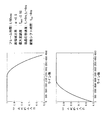
図16は、コントラストが改善された場合における、コントラストCと駆動シフト時間tとの関係を示すグラフである。同図は、光位相変調素子351をネマティック液晶により構成し、T=1/60秒、t=4ミリ秒、t=6ミリ秒、Tmax=1とした場合の、第1緑色映像のコントラストC1と、第2緑色映像のコントラストC2と、駆動シフト時間tとの関係を示す。
同図において、第1緑色映像のコントラストC1が最大となる駆動シフト時間tは、C1(t)の曲線の傾きが0となる位置、つまり式(13)により求められる。
16, in the case where the contrast is improved, which is a graph showing the relationship between the contrast C and the driving shift time t s. This figure, the optical phase modulation element 351 is constituted by a nematic liquid crystal, T = 1/60 sec, t r = 4 ms, t f = 6 ms, in the case of the T max = 1, the first green image of showing the contrast C1, the contrast C2 of the second green image, the relation between the driving shift time t s.
In the figure, the drive shift time t s of the first green image contrast C1 is maximum, a position where the slope of the curve becomes 0 C1 (t s), obtained by clogging formula (13).

Figure 0005426343
Figure 0005426343

式(13)より、式(14)に示す駆動シフト時間tが得られる。 From equation (13), the drive shift time t s shown in equation (14) is obtained.

Figure 0005426343
Figure 0005426343

光路切替制御部33は、光位相変調素子351の応答の立上り応答時間tと立下り応答時間tとを用いて式(14)を計算することにより、第1緑色映像のコントラストC1および第2緑色映像のコントラストを最大にすることができる。 The optical path switching control unit 33 calculates the expression (14) using the rising response time tr and the falling response time t f of the response of the optical phase modulation element 351, and thereby the contrast C1 and the first green video image The contrast of the two green images can be maximized.

駆動シフト時間tは、光位相変調素子351の応答の立上り応答時間tと、立下り応答時間tとを測定したり液晶等の位相変調媒体の特性データに基づいたりして、予め式(14)の計算によって求められる。または、駆動シフト時間tは、実際に投射型表示装置からの映像の投射を行って緑色映像のコントラストを測定することにより、調整により決定される。 Drive shift time t s is or based the rise response time t r of the response of the optical phase modulation element 351, the characteristic data of the phase modulation media such as liquid crystals or measuring the fall response time t f, in advance formula It is obtained by the calculation of (14). Or, the drive shift time t s by measuring the contrast of the green image by actually performing image projection from the projection type display device, is determined by the adjustment.

なお、光路切替制御部33は、光位相変調素子351の応答特性である立上り応答r(t)と立下り応答f(t)とのそれぞれに対応させて、切替制御信号SCの切替タイミングを個別に調整するようにしてもよい。   The optical path switching control unit 33 individually sets the switching timing of the switching control signal SC in correspondence with the rising response r (t) and the falling response f (t), which are the response characteristics of the optical phase modulation element 351. You may make it adjust to.

[第3の実施の形態の変形例]
上述した第3実施形態において、投射型表示装置30は、映像のフレームごとに第1緑色映像と第2緑色映像とを交互に表示するものであった。この第3実施形態の変形例では、第1緑色映像と第2緑色映像との間に黒色表示が発生する時間を設けて、第1緑色映像および第2緑色映像の映像表示時間を制限する例について説明する。
具体的には、映像信号切替装置20が、図15に示す応答の立上り時間tおよび立下り時間tにおいてON状態となるマスク制御信号を生成し、このマスク制御信号がON状態であるときに、緑色映像信号Ginの出力を遮断したり黒色画像信号に切替えたりする。これにより、光位相変調素子351の応答の立上り時間tおよび立下り時間tにおいて、緑色映像Goutによる表示を黒色にすることができる。
[Modification of Third Embodiment]
In the third embodiment described above, the projection display device 30 alternately displays the first green image and the second green image for each frame of the image. In the modification of the third embodiment, a time for generating a black display is provided between the first green image and the second green image to limit the image display time of the first green image and the second green image. Will be described.
Specifically, when the video signal switching device 20 generates a mask control signal that is turned on at the rise time tr and the fall time t f of the response shown in FIG. 15, and the mask control signal is on. In addition, the output of the green video signal Gin is cut off or switched to the black image signal. Thus, at the rise time t r and the fall time t f of the response of the optical phase modulation element 351, it is possible to display by green image Gout black.

第1緑色映像および第2緑色映像それぞれのフレームにおける表示時間をαT(0<α<1)とし、条件として、αT<T−tr,αT<T−tfとすると、領域S1、領域N1、領域S2、および領域N2は、それぞれ式(15)から式(18)で表される。   If the display time in each frame of the first green video and the second green video is αT (0 <α <1) and αT <T-tr, αT <T-tf as conditions, the region S1, the region N1, and the region S2 and the region N2 are expressed by Expression (15) to Expression (18), respectively.

Figure 0005426343
Figure 0005426343

Figure 0005426343
Figure 0005426343

Figure 0005426343
Figure 0005426343

Figure 0005426343
Figure 0005426343

ここで、式(19)のように定義すると、式(15)および式(16)は、式(20)および式(21)となる。   Here, if it defines like Formula (19), Formula (15) and Formula (16) will turn into Formula (20) and Formula (21).

Figure 0005426343
Figure 0005426343

Figure 0005426343
Figure 0005426343

Figure 0005426343
Figure 0005426343

図17は、黒色の挿入によりコントラストが改善された場合における、コントラストCと駆動シフト時間tとの関係を示すグラフである。同図は、光位相変調素子351をネマティック液晶により構成し、T=1/60秒、t=4ミリ秒、t=4ミリ秒、Tmax=0.95、α=0.5とした場合の、第1緑色映像のコントラストC1と、第2緑色映像のコントラストC2と、駆動シフト時間tとの関係を示す。同図において明らかなように、黒色を挿入することにより、図16に示した第3実施形態よりもコントラストを向上することができる。 17, in the case where the contrast is improved by the insertion of the black is a graph showing the relationship between the contrast C and the driving shift time t s. This figure, the optical phase modulation element 351 is constituted by a nematic liquid crystal, T = 1/60 sec, t r = 4 ms, t f = 4 ms, T max = 0.95, α = 0.5 and in the case of shows the contrast C1 of the first green image, and the contrast C2 of the second green image, the relation between the driving shift time t s. As can be seen in the figure, by inserting black, the contrast can be improved compared to the third embodiment shown in FIG.

[第4の実施の形態]
第1実施形態における投射型表示装置30の光学ユニット部31に含まれる青色光表示素子316、赤色光表示素子320、および緑色光表示素子322が、例えば液晶表示素子である場合、その駆動方法の制限により表示画面全体の一括書換えを行うことができない。図18は、緑色光表示素子322を液晶表示素子とした場合の第1緑色映像のフレームから第2緑色映像のフレームに書き換わる状態(フレーム上書きの状態)を模式的に示す図である。同図(a)は、前回フレーム画像である第1緑色映像のフレームG1から、現在フレーム画像である第2緑色映像のフレームG2に書き換わる最中の表示面の様子を示したものである。同図(b)は、映像のフレームが順次書き換わる様子を時系列的に示した図であり、横方向が時間方向であり、縦方向が画面の水平ラインである。同図(a),(b)が示すように、前回フレーム画像に現在フレーム画像が上書きされている途中段階では、同一表示画面上にフレームG1およびフレームG2の2つのフレーム画像が混在する状態となる。
[Fourth Embodiment]
When the blue light display element 316, the red light display element 320, and the green light display element 322 included in the optical unit 31 of the projection display device 30 in the first embodiment are liquid crystal display elements, for example, Due to restrictions, the entire display screen cannot be rewritten at once. FIG. 18 is a diagram schematically showing a state (frame overwriting state) in which the first green video frame is rewritten to the second green video frame when the green light display element 322 is a liquid crystal display element. FIG. 5A shows the state of the display surface during the rewriting of the first green video frame G1 as the previous frame image to the second green video frame G2 as the current frame image. FIG. 4B is a diagram showing, in time series, how video frames are sequentially rewritten, with the horizontal direction being the time direction and the vertical direction being the horizontal lines of the screen. As shown in FIGS. 6A and 6B, in the middle stage where the current frame image is overwritten on the previous frame image, two frame images of the frames G1 and G2 are mixed on the same display screen. Become.

そこで、本実施形態では、第1緑色映像のフレームG1と第2緑色映像のフレームG2との間に黒色のフレーム画像を挿入し、切替制御信号SCのOFF状態とON状態との切替え周期を2倍にするとともに、水平ラインごとに、切替制御信号SCの位相を水平表示期間ずつずらすようにする。
具体的には、映像信号切替装置20が、第1緑色映像信号G1inの第1緑色フレーム画像と第2緑色映像信号G2inの第2緑色フレーム画像との間に1フレーム分の黒色画像を挿入して緑色映像信号Ginとして出力する。
また、信号発生装置10は、映像制御信号の中の水平同期信号をフレーム同期信号FTとともに光路切替制御部33に供給し、光路切替制御部33は、水平同期信号とフレーム同期信号FTとに基づいて、フレーム同期信号FTの周期の2倍周期であって、水平ラインごとに位相が水平表示期間ずつずれるタイミングである切替制御信号SCを生成して光路シフト部32に供給する。
図19は、フレーム画像の切替わりと切替制御信号SCとの関係を模式的に示す図である。同図は、先頭ライン(Top)から最終ライン(Bottom)までの水平ラインのうち、先頭ライン(Top)と中間ライン(Middle)と最終ライン(Bottom)とに対応する切替制御信号SCのタイミングを示すものである。
Therefore, in the present embodiment, a black frame image is inserted between the first green video frame G1 and the second green video frame G2, and the switching cycle of the switching control signal SC between the OFF state and the ON state is set to 2. In addition, the phase of the switching control signal SC is shifted by the horizontal display period for each horizontal line.
Specifically, the video signal switching device 20 inserts a black image for one frame between the first green frame image of the first green video signal G1in and the second green frame image of the second green video signal G2in. And output as a green video signal Gin.
The signal generator 10 supplies the horizontal synchronization signal in the video control signal to the optical path switching control unit 33 together with the frame synchronization signal FT. The optical path switching control unit 33 is based on the horizontal synchronization signal and the frame synchronization signal FT. Thus, a switching control signal SC having a cycle twice the cycle of the frame synchronization signal FT and the phase being shifted for each horizontal line by the horizontal display period is generated and supplied to the optical path shift unit 32.
FIG. 19 is a diagram schematically illustrating the relationship between the switching of frame images and the switching control signal SC. This figure shows the timing of the switching control signal SC corresponding to the first line (Top), the middle line (Middle), and the last line (Bottom) among the horizontal lines from the first line (Top) to the last line (Bottom). It is shown.

[第5の実施の形態]
本発明の第5実施形態では、第1実施形態における光路シフト部32に含まれる光位相変調素子351を、映像のフレームの中間ライン付近で2分割して各光位相変調素子を切替えの位相をずらして駆動させる例について説明する。
図20は、本実施形態である映像光出力装置に含まれる光路シフト部と光路切替制御部との機能構成を示すブロック図である。同図において、光路切替制御部33bは、信号発生装置10からフレーム同期信号FTの供給を受けて、緑色光表示素子322の表示部の先頭ラインから中間付近のラインまでを含む上半分フレームを切替え制御するための切替制御信号SCUと、緑色光表示素子322の表示部の中間付近のラインから最終ラインまでを含む下半分フレームを切替え制御するための切替制御信号SCDとを生成する。
[Fifth Embodiment]
In the fifth embodiment of the present invention, the optical phase modulation element 351 included in the optical path shift unit 32 in the first embodiment is divided into two near the middle line of the video frame, and the phase of switching each optical phase modulation element is changed. An example of driving by shifting will be described.
FIG. 20 is a block diagram illustrating functional configurations of an optical path shift unit and an optical path switching control unit included in the video light output apparatus according to the present embodiment. In the same figure, the optical path switching control unit 33b receives the supply of the frame synchronization signal FT from the signal generator 10, and switches the upper half frame including the first line of the display unit of the green light display element 322 to the line near the middle. A switching control signal SCU for controlling and a switching control signal SCD for switching control of the lower half frame including the line near the middle of the display portion of the green light display element 322 to the last line are generated.

光路シフト部32bは、光学ユニット部31から、赤色映像光Rlpと、緑色映像光Gcpと、青色映像光Blpとの供給を受けるとともに、光路切替制御部33bから切替制御信号SCU,SCDの供給を受ける。
光路シフト部32bは、切替制御信号SCUの切替タイミングにしたがって、赤色映像光Rlpによる赤色映像と、青色映像光Blpによる青色映像と、緑色映像光Gcpにおける第1緑色映像との上半分フレーム上の画素位置が一致するとともに、緑色映像光Gcpにおける第2緑色映像の上半分フレーム上の画素位置が第1緑色映像の上半分フレーム上の画素位置に対して垂直方向に1画素分以下(例えば、0.5画素分)ずれるように光路を設定した赤色映像光RUoutと、緑色映像光GUoutと、青色映像光BUoutとを出力する。
The optical path shift unit 32b receives supply of the red video light Rlp, the green video light Gcp, and the blue video light Blp from the optical unit 31, and supplies the switching control signals SCU and SCD from the optical path switching control unit 33b. receive.
The optical path shift unit 32b is on the upper half frame of the red video by the red video light Rlp, the blue video by the blue video light Blp, and the first green video by the green video light Gcp according to the switching timing of the switching control signal SCU. The pixel positions coincide with each other, and the pixel position on the upper half frame of the second green image in the green image light Gcp is equal to or less than one pixel in the vertical direction with respect to the pixel position on the upper half frame of the first green image (for example, The red video light RUout, the green video light GUout, and the blue video light BUout, whose optical paths are set so as to be shifted by 0.5 pixel), are output.

また、光路シフト部32bは、切替制御信号SCDの切替タイミングにしたがって、赤色映像光Rlpによる赤色映像と、青色映像光Blpによる青色映像と、緑色映像光Gcpにおける第1緑色映像との下半分フレーム上の画素位置が一致するとともに、緑色映像光Gcpにおける第2緑色映像の下半分フレーム上の画素位置が第1緑色映像の下半分フレーム上の画素位置に対して垂直方向に1画素分以下(例えば、0.5画素分)ずれるように光路を設定した赤色映像光RDoutと、緑色映像光GDoutと、青色映像光BDoutとを出力する。   In addition, the optical path shift unit 32b, according to the switching timing of the switching control signal SCD, the lower half frame of the red video by the red video light Rlp, the blue video by the blue video light Blp, and the first green video by the green video light Gcp. The upper pixel positions coincide with each other, and the pixel position on the lower half frame of the second green image in the green image light Gcp is one pixel or less in the vertical direction with respect to the pixel position on the lower half frame of the first green image ( For example, the red video light RDout, the green video light GDout, and the blue video light BDout whose optical paths are set to be shifted are output.

図21は、光路シフト部32bに含まれる光位相変調素子の素子表面を模式的に斜視した図である。同図(a)は、光位相変調素子の素子表面に、フレームを中間の水平ライン付近で上下に分離するように光透過性を有する電極211U,211Dが設けられた様子を示す図である。電極211Uと電極211Dとの間には、製造工程上の理由や電気特性上の理由等によって数μmの隙間が生じるため、この隙間は、位相変調されない緑色映像光が透過される部分となる。
また、同図(b)は、電極211Uと電極211Dとの隙間部分に遮光物が設けられた様子を示す図である。同図に示すように、電極211Uと電極211Dとの隙間部分には、位相変調されない緑色映像光が透過されないようにするため、遮光物212が設けられるようにしてもよい。遮光物212の材質は、例えばアルミニウムである。
同図(a)に示すような電極211U,211D間の隙間および遮光物212は、表示素子面から光学的に距離が離れており投射映像には像として現れないため画質を損なうことはない。
FIG. 21 is a schematic perspective view of the element surface of the optical phase modulation element included in the optical path shift unit 32b. FIG. 5A is a diagram showing a state in which light-transmitting electrodes 211U and 211D are provided on the element surface of the optical phase modulation element so as to separate the frame vertically in the vicinity of the intermediate horizontal line. Since a gap of several μm is generated between the electrode 211U and the electrode 211D for reasons of the manufacturing process, reasons of electrical characteristics, and the like, this gap is a portion through which green image light that is not phase-modulated is transmitted.
FIG. 5B is a diagram showing a state in which a light shielding object is provided in a gap portion between the electrode 211U and the electrode 211D. As shown in the figure, a light shielding member 212 may be provided in a gap portion between the electrode 211U and the electrode 211D so that green image light that is not phase-modulated is not transmitted. The material of the light shield 212 is, for example, aluminum.
The gap between the electrodes 211U and 211D and the light shield 212 as shown in FIG. 5A are optically separated from the display element surface and do not appear as an image in the projected image, so that the image quality is not impaired.

図22は、フレーム同期信号FTと切替制御信号SCUと切替制御信号SCDとの動作タイミングを示すタイミングチャートである。同図に示すように、フレーム同期信号FTは、第1実施形態と同様に、映像のフレーム周期で各フレームの先頭の所定期間にパルスを発生する信号である。
切替制御信号SCU、SCDは、フレーム同期信号FTの2倍の周期で、OFF状態とON状態とを交互に繰り返すトグル信号であり、OFF状態を0(ゼロ)値とし、ON状態を任意のレベル値とする。切替制御信号SCU,SCDともに、黒色映像フレームの期間中に状態を切替えるような動作タイミングとし、切替制御信号SDCは、切替制御信号SCUに対して駆動シフト時間tsc分位相を遅くずらすようにする。駆動シフト時間tscは、1フレーム時間の約半分程度が好ましい。切替制御信号SCU,SCDがOFF状態である期間は、第1緑色フレーム映像のフレーム期間に対応し、切替制御信号SCU,SCDがON状態である期間は、第2緑色フレーム映像のフレーム期間に対応する。
FIG. 22 is a timing chart showing operation timings of the frame synchronization signal FT, the switching control signal SCU, and the switching control signal SCD. As shown in the figure, the frame synchronization signal FT is a signal that generates a pulse in a predetermined period at the head of each frame in the frame period of the video, as in the first embodiment.
The switching control signals SCU and SCD are toggle signals that alternately repeat the OFF state and the ON state at a cycle twice that of the frame synchronization signal FT. The OFF state is a 0 (zero) value, and the ON state is an arbitrary level. Value. Both the switching control signals SCU and SCD have an operation timing for switching the state during the black video frame period, and the switching control signal SDC is shifted in phase by the drive shift time t sc with respect to the switching control signal SCU. . The drive shift time t sc is preferably about half of one frame time. The period in which the switching control signals SCU and SCD are in the OFF state corresponds to the frame period of the first green frame video, and the period in which the switching control signals SCU and SCD are in the ON state corresponds to the frame period of the second green frame video. To do.

図23は、本実施形態における光位相変調素子を用いた場合の、水平ライン数とコントラストとの関係を示すグラフである。同図は、光位相変調素子をネマティック液晶により構成し、T=1/60秒、t=4ミリ秒、t=4ミリ秒、α=0.5、Tmax=0.95、tsc=4ミリ秒とした場合の、水平ライン数と第1緑色映像のコントラストC1との関係を示す。
同図によれば、フレーム全体にわたって、第1緑色映像のコントラストC1はほぼ“1”となる。
なお、光位相変調素子351の分割数は2分割に限らず3以上に分割してもよい。その場合、光路切替制御部33bは、時間をずらしてそれぞれの領域を駆動するようにする。
FIG. 23 is a graph showing the relationship between the number of horizontal lines and contrast when the optical phase modulation element of this embodiment is used. This figure, the optical phase modulation element constituted by a nematic liquid crystal, T = 1/60 sec, t r = 4 ms, t f = 4 ms, α = 0.5, T max = 0.95, t The relationship between the number of horizontal lines and the contrast C1 of the first green image when sc = 4 milliseconds is shown.
According to the figure, the contrast C1 of the first green image is substantially “1” over the entire frame.
The number of divisions of the optical phase modulation element 351 is not limited to two and may be divided into three or more. In that case, the optical path switching control unit 33b drives each region while shifting the time.

[第6の実施の形態]
本実施形態では、図18に示したような不要な残像光が投射されるのを防ぐために、物理的なシャッタ機構を、光位相変調素子351の後段の所望の場所に配置して、残像光を遮光する例について説明する。
図24は、物理的なシャッタ機構である回転シャッタを、映像光の入射側より模式的に表した図である。同図に示すように、回転シャッタ241は、円板上のシャッタ板242に複数の扇形状の開口部243が設けられる。そして、回転シャッタ241は、例えば、投射型表示装置30内の光路シフト部32と投射光学系34との間に、赤色映像光Routと緑色映像光Goutと青色映像光Boutとの光束が開口部243を通過する位置に設けられる。
[Sixth Embodiment]
In the present embodiment, in order to prevent unnecessary afterimage light as shown in FIG. 18 from being projected, a physical shutter mechanism is disposed at a desired location after the optical phase modulation element 351 to provide afterimage light. An example of shielding light will be described.
FIG. 24 is a diagram schematically showing a rotary shutter, which is a physical shutter mechanism, from the image light incident side. As shown in the figure, the rotary shutter 241 is provided with a plurality of fan-shaped openings 243 in a shutter plate 242 on a circular plate. The rotary shutter 241 has, for example, a light beam of red video light Rout, green video light Gout, and blue video light Bout between the optical path shift unit 32 and the projection optical system 34 in the projection display device 30. It is provided at a position passing through H.243.

回転シャッタ241の回転角速度と開口部243の位置とは、図18(a)に示す前回フレームの映像光が遮光されるように予め設定し調整される。
なお、回転シャッタ241は、投射光学系34とスクリーンとの間に設けられてもよい。
The rotational angular velocity of the rotary shutter 241 and the position of the opening 243 are set and adjusted in advance so that the image light of the previous frame shown in FIG.
The rotary shutter 241 may be provided between the projection optical system 34 and the screen.

[第7の実施の形態]
第1実施形態では、投射型表示装置30に1つの光路シフト部32を設けて画面上垂直方向に0.5画素分の画素ずらしを行う例について説明した。本実施形態では、光路シフト部をN段(Nは2以上の整数)設けて、映像光の光路シフトを2のN乗通りにする例について説明する。
図25は、本実施形態である映像光出力装置における光路シフト部の機能構成を示すブロック図である。同図に示すように、本実施形態における光路シフト部32cは、第1実施形態における光路シフト部32内部の構成の最終段にλ/4板355を追加した構成を有する。λ/4板355は、複屈折光学素子353から供給された映像光のうち、緑色光波長成分についての偏光状態を、垂直または水平の直線偏光から右円偏光に変換するものである。
[Seventh Embodiment]
In the first embodiment, the example in which one optical path shift unit 32 is provided in the projection display device 30 and the pixel shift is performed by 0.5 pixels in the vertical direction on the screen has been described. In the present embodiment, an example will be described in which N stages of optical path shift units (N is an integer of 2 or more) are provided, and the optical path shift of image light is set to 2 to the Nth power.
FIG. 25 is a block diagram illustrating a functional configuration of an optical path shift unit in the video light output apparatus according to the present embodiment. As shown in the figure, the optical path shift unit 32c in the present embodiment has a configuration in which a λ / 4 plate 355 is added to the final stage of the configuration inside the optical path shift unit 32 in the first embodiment. The λ / 4 plate 355 converts the polarization state of the green light wavelength component of the image light supplied from the birefringent optical element 353 from vertical or horizontal linearly polarized light to right circularly polarized light.

図26は、光路シフト部32cを4段適用した場合の、光路シフト部32c−1〜32c−4と光路切替制御部との機能構成を示すブロック図である。同図において、光路切替制御部33cは、信号発生装置10からフレーム同期信号FTの供給を受けて、映像の16フレーム期間で16通りの状態の組み合わせとなるような切替制御信号SC1,SC2,SC3,SC4を生成して出力する。例えば、光路切替制御部33cは、フレーム同期信号FTを入力信号として入力パルスをカウントアップするカウンタ演算処理部を含めて構成する。光路シフト部32c−1〜32c−4は、4つ(N=4)の光路シフト部32cをカスケード接続したものである。   FIG. 26 is a block diagram illustrating a functional configuration of the optical path shift units 32c-1 to 32c-4 and the optical path switching control unit when the four stages of optical path shift units 32c are applied. In the figure, the optical path switching control unit 33c receives the supply of the frame synchronization signal FT from the signal generator 10 and switches the switching control signals SC1, SC2, SC3 so that 16 combinations of states are obtained in 16 frame periods of the video. , SC4 is generated and output. For example, the optical path switching control unit 33c includes a counter calculation processing unit that counts up an input pulse using the frame synchronization signal FT as an input signal. The optical path shift units 32c-1 to 32c-4 are obtained by cascading four (N = 4) optical path shift units 32c.

図26に示すように4つの光路シフト部32cをカスケード接続した場合、2の4乗=16通りの光路を実現することができる。光路シフト部32c単体の光路シフト量は、複屈折光学素子353に含まれる複屈折媒体の光進行方向の厚みで定まるため、各光路シフト部32の画素ずらし方向と、複屈折媒体の厚みとをそれぞれ同一にすることにより、整数倍の光路シフト量を得ることができる。
また、画素ずらし法によって高解像度化を実現するためには、画素の位置精度を、1画素の約20分の1以上の精度とすることが要求される。よって、光路シフト部32cをN段設けることにより、2のN乗分の1の精度で画素ずらしの量を微調整することが可能となる。
As shown in FIG. 26, when four optical path shift units 32c are cascade-connected, 2 4 = 16 optical paths can be realized. Since the optical path shift amount of the optical path shift unit 32c alone is determined by the thickness of the birefringent medium included in the birefringent optical element 353 in the light traveling direction, the pixel shift direction of each optical path shift unit 32 and the thickness of the birefringent medium are determined. By making them the same, an integral multiple optical path shift amount can be obtained.
In addition, in order to achieve high resolution by the pixel shifting method, it is required that the pixel position accuracy be about 1/20 of that of one pixel. Therefore, by providing N stages of optical path shift units 32c, it is possible to finely adjust the amount of pixel shift with an accuracy of 1 / N.

[第8の実施の形態]
本発明の第8実施形態は、複屈折光学素子による光路シフトのシフト量を調整することを可能にする例について説明する。本実施形態における光路シフト部は、第1実施形態における複屈折光学素子353の代わりに、光路シフト量を調整可能な複屈折光学部を設ける。図27は、本実施形態である映像光出力装置における光路シフト部に含まれる複屈折光学部の概略の構成を示すブロック図である。同図に示すように、複屈折光学部271は、2枚の複屈折板を貼り合わせて楔形状にした楔形サバール板271a,271bを含む。そして、複屈折光学部271は、楔形サバール板271a,271bを、それぞれの厚みの狭い方の端部同士が映像光の入射方向に相互にずれて突き合うようにして組み合わされる。楔形サバール板271aは、映像光の入射方向に対して垂直方向である矢印Aの方向に前後に可動に配置されるとともに、楔形サバール板261bは固定配置される。
複屈折光学部271は、楔形サバール板271aを矢印Aの方向に前後させることにより、楔形サバール板271bから射出される光線の常光線と異常光線との距離、すなわち光路シフト量dを調整することができる。
[Eighth Embodiment]
In the eighth embodiment of the present invention, an example in which the shift amount of the optical path shift by the birefringent optical element can be adjusted will be described. The optical path shift unit in the present embodiment is provided with a birefringent optical unit capable of adjusting the optical path shift amount, instead of the birefringent optical element 353 in the first embodiment. FIG. 27 is a block diagram showing a schematic configuration of a birefringence optical unit included in the optical path shift unit in the image light output device according to the present embodiment. As shown in the figure, the birefringent optical unit 271 includes wedge-shaped saval plates 271a and 271b in which two birefringent plates are bonded to form a wedge shape. The birefringent optical unit 271 is combined with the wedge-shaped Savart plates 271a and 271b such that the narrower ends of the wedge-shaped Savart plates 271a and 271b are offset from each other in the image light incident direction. The wedge-shaped sabal plate 271a is movably disposed back and forth in the direction of arrow A, which is perpendicular to the incident direction of the image light, and the wedge-shaped savar plate 261b is fixedly disposed.
The birefringent optical unit 271 adjusts the distance d between the ordinary ray and the extraordinary ray of the light beam emitted from the wedge-shaped savar plate 271b by moving the wedge-shaped savar plate 271a back and forth in the direction of arrow A. Can do.

[その他の実施の形態]
本発明の第1実施形態では、投射型表示装置30は、光路シフト部32を光学ユニット部31と投射光学系34との間に設けた構成を有していた。この光路シフト部32の配置位置はこれに限らず、例えば、光路シフト部32は、投射光学系34を通した後に配置されてもよい。
また、第1実施形態では、三原色による各映像のうち緑色映像について画素ずらしを行う例について説明したが、この画素ずらしを行う映像は、緑色映像に限らず任意の色の映像としてよい。つまり、第1実施形態に示したように、信号発生装置10は、画素をずらす特定色映像について2種類の特定色映像信号(第1および第2の映像光)を映像信号切替装置20に供給して映像のフレームごとに切替えさせ、光学ユニット部31は、特定色映像を右円偏光の偏光状態にして出力するとともに、特定映像以外の映像(第3の映像光)を縦方向の直線偏光にして出力する。
[Other embodiments]
In the first embodiment of the present invention, the projection display device 30 has a configuration in which the optical path shift unit 32 is provided between the optical unit unit 31 and the projection optical system 34. The arrangement position of the optical path shift unit 32 is not limited to this. For example, the optical path shift unit 32 may be arranged after passing through the projection optical system 34.
In the first embodiment, an example in which pixel shifting is performed on a green image among the images of the three primary colors has been described. However, the image on which pixel shifting is performed is not limited to a green image and may be an image of any color. That is, as shown in the first embodiment, the signal generation device 10 supplies the video signal switching device 20 with two types of specific color video signals (first and second video lights) for the specific color video in which the pixels are shifted. Then, the optical unit 31 outputs the specific color image in the right circular polarization polarization state and outputs the image other than the specific image (third image light) in the vertical linear polarization direction. And output.

また、第1実施形態は、順次走査(プログレッシブ)映像を対象とした例について説明したが、これ以外にも、飛越し走査(インターレース)映像にも適用することができる。この飛越し走査映像を用いた場合の投射型表示システムは、フレーム周期FTの代わりに、飛越し走査映像のフィールド周期に同期したフィールド同期信号を用いて、第1緑色映像信号G1inと第2緑色映像信号G2inとを垂直方向に1画素分ずらすようにする。
また、第1実施形態では、映像光出力装置を投射型表示装置30に含めた例について説明した。これ以外にも、本発明の実施形態である映像光出力装置は、液晶ディスプレイ、有機EL(Electro−Luminescence)ディスプレイ、プラズマディスプレイ等の直視型ディスプレイ装置にも適用できる。この場合、映像光出力装置は、直視型ディスプレイ装置に含まれる表示素子の表示発光後の位置に組み込まれるようにすればよい。
In addition, although the first embodiment has been described with respect to an example in which progressive scanning video is targeted, the present invention can be applied to interlaced video in addition to this. In the projection display system using the interlaced scanning image, the first green image signal G1in and the second green color are used by using a field synchronization signal synchronized with the field period of the interlaced scanning image instead of the frame period FT. The video signal G2in is shifted by one pixel in the vertical direction.
In the first embodiment, the example in which the image light output device is included in the projection display device 30 has been described. In addition, the image light output device according to the embodiment of the present invention can be applied to a direct-view display device such as a liquid crystal display, an organic EL (Electro-Luminescence) display, and a plasma display. In this case, the image light output device may be incorporated at a position after the display light emission of the display element included in the direct view display device.

本発明の第4実施形態から第6実施形態までの各実施形態では、黒の映像信号を挿入する例(第4および第5実施形態)と回転シャッタ241を使用する例(第6実施形態)とについて説明した。これ以外にも、例えば、光学ユニット部31に含まれる光源部311を点滅させることによって、各表示素子からの映像読出し光を間欠的に発光させ、投射型表示装置30が不要な残像光を投射する等の画質劣化を防止することができる。このように動作させる場合の光源部311として、高速な点滅動作が可能なLED(Light Emitting Diode)光源を適用することが望ましい。   In each of the fourth to sixth embodiments of the present invention, an example in which a black video signal is inserted (fourth and fifth embodiments) and an example in which a rotary shutter 241 is used (sixth embodiment). And explained. In addition to this, for example, by blinking the light source unit 311 included in the optical unit unit 31, video readout light from each display element is intermittently emitted, and the projection display device 30 projects unnecessary afterimage light. It is possible to prevent the image quality from deteriorating. It is desirable to apply an LED (Light Emitting Diode) light source capable of high-speed blinking operation as the light source unit 311 in the case of operating in this way.

本発明の第3実施形態から第8実施形態までの各実施形態は、第1実施形態をもとにした実施形態として説明したが、これらのうち第3実施形態から第6実施形態と第8実施形態とについては、第2実施形態をもとにすることができる。   Each embodiment from the third embodiment to the eighth embodiment of the present invention has been described as an embodiment based on the first embodiment. Among these, the third embodiment to the sixth embodiment and the eighth embodiment are described. About embodiment, it can be based on 2nd Embodiment.

上述した各実施形態による投射型表示システムは、立体映像表示システムに適用するこができる。例えば、図28に示すように、本発明の各実施形態による投射型表示システムからの投射光を、要素レンズが多数配置されたマイクロレンズアレイやレンチキュラーが設けられた複眼レンズ配列板40を介して投影する。これにより、画素ずらしをした高精細映像や超高精細映像の立体映像を投影表示することができる。   The projection display system according to each of the embodiments described above can be applied to a stereoscopic video display system. For example, as shown in FIG. 28, the projection light from the projection display system according to each embodiment of the present invention is transmitted through a compound eye lens array plate 40 provided with a microlens array in which a large number of element lenses are arranged and a lenticular. Project. As a result, it is possible to project and display a high-definition video and a super-high-definition stereoscopic video in which pixels are shifted.

また、上述した各実施形態による投射型表示システムは、赤色映像と青色映像と第1緑色映像とのフレーム上の画素位置が一致するとともに、第2緑色映像のフレーム上の画素位置が第1緑色映像のフレーム上の画素位置に対して垂直方向に1画素未満分(例えば、0.5画素分)ずれるように光路シフトの方向を設定することによって、緑色映像のみの垂直方向の解像度を、画素ずらしをしない場合の解像度の2倍にする例であった。
投射型表示システムは、上記の例以外に、第2緑色映像のフレーム上の画素位置が第1緑色映像のフレーム上の画素位置に対して水平方向に1画素未満分(例えば、0.5画素分)ずれるように光路シフトの方向を設定してもよい。これによって、投射型表示システムは、緑色映像のみの水平方向の解像度を、画素ずらしをしない場合の解像度の2倍にすることができる。
また、投射型表示システムは、第2緑色映像のフレーム上の画素位置が第1緑色映像のフレーム上の画素位置に対して水平方向および垂直方向にそれぞれ1画素未満分(例えば、それぞれ0.5画素分)ずれるように(つまり、斜め方向にずれるように)光路シフトの方向を設定してもよい。これによって、投射型表示システムは、緑色映像のみの水平方向および垂直方向それぞれの解像度を、画素ずらしをしない場合の解像度の2倍にすることができる。
In addition, in the projection display systems according to the above-described embodiments, the pixel positions on the frames of the red video, the blue video, and the first green video match, and the pixel positions on the frame of the second green video are the first green. By setting the optical path shift direction so that it is shifted by less than one pixel (for example, 0.5 pixel) in the vertical direction with respect to the pixel position on the video frame, the vertical resolution of only the green video is set to the pixel. In this example, the resolution is doubled when the shift is not performed.
In the projection display system, in addition to the above example, the pixel position on the second green video frame is less than one pixel in the horizontal direction with respect to the pixel position on the first green video frame (for example, 0.5 pixel). The direction of the optical path shift may be set so as to deviate. Accordingly, the projection display system can double the horizontal resolution of only the green image to the resolution when the pixel is not shifted.
Further, the projection display system has a pixel position on the second green image frame that is less than one pixel in the horizontal direction and the vertical direction with respect to the pixel position on the first green image frame (for example, 0.5 pixels each). The direction of the optical path shift may be set so as to be shifted (by a pixel) (that is, shifted in an oblique direction). Thus, the projection display system can double the resolution in the horizontal direction and the vertical direction of only the green image to the resolution in the case where the pixel is not shifted.

以上、本発明の実施の形態について図面を参照して詳述したが、具体的な構成はこの実施形態に限られるものではなく、本発明の要旨を逸脱しない範囲の設計等も含まれる。   As mentioned above, although embodiment of this invention was explained in full detail with reference to drawings, the concrete structure is not restricted to this embodiment, The design etc. of the range which does not deviate from the summary of this invention are included.

1 投射型表示システム
10 信号発生装置
20 映像信号切替装置
30 投射型表示装置
31 光学ユニット部
32,32a,32b,32c 光路シフト部
33,33b,33c 光路切替制御部
34 投射光学系
40 複眼レンズ配列板
211D,211U 電極
212 遮光物
241 回転シャッタ
242 シャッタ版
243 開口部
271 複屈折光学部
271a,271b 楔形サバール板
351,351a 光位相変調素子
352 位相板
353 複屈折光学素子
354 偏光板
355 λ/4板
DESCRIPTION OF SYMBOLS 1 Projection type display system 10 Signal generator 20 Image | video signal switching device 30 Projection type display device 31 Optical unit part 32, 32a, 32b, 32c Optical path shift part 33, 33b, 33c Optical path switching control part 34 Projection optical system 40 Compound eye lens arrangement | sequence Plates 211D and 211U Electrodes 212 Shields 241 Rotating shutters 242 Shutter plates 243 Openings 271 Birefringent optical units 271a and 271b Wedge-shaped Savart plates 351 and 351a Optical phase modulation elements 352 Phase plates 353 Birefringent optical elements 354 Polarizing plates 355 λ / 4 Board

Claims (1)

所定周期で第1および第2の状態が交互に切替わる切替制御信号を出力する光路切替制御部と、
所定色の第1および第2の映像光が前記所定周期で交互に切替わる前記所定色の映像光と、前記所定色とは異なる色の第3の映像光との供給を受けるとともに、前記光路切替制御部から前記切替制御信号の供給を受けて、前記切替制御信号が前記第1の状態であるときは、前記第1および第3の映像光を、当該映像光出力装置の入出力間の光路をそれぞれずらさずに出力する一方、前記切替制御信号が前記第2の状態であるときは、前記第2の映像光を当該映像光出力装置の入力側に対し光路をずらして出力側に出力する光路シフト部と、
を備え
前記光路シフト部は、
前記所定色の映像光と前記第3の映像光との供給を受けて、前記所定色の映像光についてはこれを分光して一方の映像光を直進透過させるとともに他方の映像光を屈折させて光路をシフトして透過させ、前記第3の映像光についてはこれを直進透過させる複屈折光学部と、
前記切替制御信号が前記第1の状態であるときは、前記複屈折光学部からの第1の出力映像光について偏光方向を変調しない一方、前記切替制御信号が前記第2の状態であるときは、前記第1の出力映像光について偏光方向を変調する光位相変調部と、
この光位相変調部からの第2の出力映像光について、所定の偏光方向成分の映像光のみを透過させる偏光板と、
を備えることを特徴とする映像光出力装置。
An optical path switching control unit for outputting a switching control signal for alternately switching the first and second states at a predetermined period;
The first and second image lights of a predetermined color are supplied with the image light of the predetermined color that is alternately switched at the predetermined period and the third image light of a color different from the predetermined color, and the optical path When the switching control signal is supplied from the switching control unit and the switching control signal is in the first state, the first and third video lights are transmitted between the input and output of the video light output device. While the optical path is output without shifting, when the switching control signal is in the second state, the second video light is output to the output side while shifting the optical path with respect to the input side of the video light output device. An optical path shift unit,
Equipped with a,
The optical path shift unit is
The video light of the predetermined color and the third video light are supplied, and the video light of the predetermined color is split to transmit one video light straight and refract the other video light. A birefringent optical unit that shifts and transmits the optical path and transmits the third image light in a straight line; and
When the switching control signal is in the first state, the polarization direction of the first output image light from the birefringent optical unit is not modulated, while when the switching control signal is in the second state , An optical phase modulator that modulates the polarization direction of the first output image light;
For the second output video light from the optical phase modulation unit, a polarizing plate that transmits only video light of a predetermined polarization direction component,
Video light output device according to claim Rukoto equipped with.
JP2009275673A 2009-12-03 2009-12-03 Image light output device Expired - Fee Related JP5426343B2 (en)

Priority Applications (1)

Application Number Priority Date Filing Date Title
JP2009275673A JP5426343B2 (en) 2009-12-03 2009-12-03 Image light output device

Applications Claiming Priority (1)

Application Number Priority Date Filing Date Title
JP2009275673A JP5426343B2 (en) 2009-12-03 2009-12-03 Image light output device

Publications (2)

Publication Number Publication Date
JP2011118165A JP2011118165A (en) 2011-06-16
JP5426343B2 true JP5426343B2 (en) 2014-02-26

Family

ID=44283579

Family Applications (1)

Application Number Title Priority Date Filing Date
JP2009275673A Expired - Fee Related JP5426343B2 (en) 2009-12-03 2009-12-03 Image light output device

Country Status (1)

Country Link
JP (1) JP5426343B2 (en)

Families Citing this family (1)

* Cited by examiner, † Cited by third party
Publication number Priority date Publication date Assignee Title
JP6028914B2 (en) * 2012-12-13 2016-11-24 セイコーエプソン株式会社 Image display system

Family Cites Families (5)

* Cited by examiner, † Cited by third party
Publication number Priority date Publication date Assignee Title
JP2003207747A (en) * 2002-01-11 2003-07-25 Ricoh Co Ltd Image display optical unit, image display, and image display method
JP5073195B2 (en) * 2004-11-02 2012-11-14 株式会社リコー Image display device and image projection device
JP2007065483A (en) * 2005-09-01 2007-03-15 Olympus Corp Image display device
JP2007163943A (en) * 2005-12-15 2007-06-28 Olympus Corp Image display device
JP2008164811A (en) * 2006-12-27 2008-07-17 Olympus Corp Image display method and image display device

Also Published As

Publication number Publication date
JP2011118165A (en) 2011-06-16

Similar Documents

Publication Publication Date Title
US7202917B2 (en) Projection type image display device
JP3721641B2 (en) Video projection device
JPH09152572A (en) Image processor, image display device, and image pickup device
JP6070127B2 (en) Image display device and image display system
JP2004205919A (en) Projection type stereoscopic display device
JP3784279B2 (en) Projection-type image display device
JP5104096B2 (en) 3D image display apparatus and 3D image display method
JP2008209476A (en) Stereoscopic image display device
US7106389B2 (en) Optical shifter and projection type optical display system
US9075300B2 (en) Projector
JP3722205B2 (en) Projection-type image display device
JP3722204B2 (en) Projection-type image display device
JP3297191B2 (en) Projection display device
JP3891000B2 (en) Liquid crystal display device and driving method thereof
US6817718B2 (en) Projection type optical display system
JP2006058588A (en) Optical device, optical apparatus, display apparatus and stereoscopic image display apparatus
JP5059446B2 (en) Display device, projection display device, optical path shift element control circuit, and optical path shift element
JPH0752262B2 (en) 6-panel LCD projector
US11095862B2 (en) Optical module having pixel shifting mechanism transitioning to first state or second state, method for controlling the same, and projection-type display apparatus
JP5426343B2 (en) Image light output device
JP2010278955A (en) Image processing apparatus, electro-optical device, display method, and electronic apparatus
JP2002207192A (en) Video display unit and driving circuit
JP2012208216A (en) Projection type display device
JP2005057457A (en) Apparatus and method for image projection
JPH07318884A (en) Stereoscopic video display device

Legal Events

Date Code Title Description
A621 Written request for application examination

Free format text: JAPANESE INTERMEDIATE CODE: A621

Effective date: 20120322

A977 Report on retrieval

Free format text: JAPANESE INTERMEDIATE CODE: A971007

Effective date: 20130322

A131 Notification of reasons for refusal

Free format text: JAPANESE INTERMEDIATE CODE: A131

Effective date: 20130820

A521 Request for written amendment filed

Free format text: JAPANESE INTERMEDIATE CODE: A523

Effective date: 20131001

TRDD Decision of grant or rejection written
A01 Written decision to grant a patent or to grant a registration (utility model)

Free format text: JAPANESE INTERMEDIATE CODE: A01

Effective date: 20131029

A61 First payment of annual fees (during grant procedure)

Free format text: JAPANESE INTERMEDIATE CODE: A61

Effective date: 20131128

R150 Certificate of patent or registration of utility model

Ref document number: 5426343

Country of ref document: JP

Free format text: JAPANESE INTERMEDIATE CODE: R150

Free format text: JAPANESE INTERMEDIATE CODE: R150

R250 Receipt of annual fees

Free format text: JAPANESE INTERMEDIATE CODE: R250

R250 Receipt of annual fees

Free format text: JAPANESE INTERMEDIATE CODE: R250

R250 Receipt of annual fees

Free format text: JAPANESE INTERMEDIATE CODE: R250

R250 Receipt of annual fees

Free format text: JAPANESE INTERMEDIATE CODE: R250

R250 Receipt of annual fees

Free format text: JAPANESE INTERMEDIATE CODE: R250

R250 Receipt of annual fees

Free format text: JAPANESE INTERMEDIATE CODE: R250

LAPS Cancellation because of no payment of annual fees