JP5308078B2 - Photocathode - Google Patents
Photocathode Download PDFInfo
- Publication number
- JP5308078B2 JP5308078B2 JP2008155777A JP2008155777A JP5308078B2 JP 5308078 B2 JP5308078 B2 JP 5308078B2 JP 2008155777 A JP2008155777 A JP 2008155777A JP 2008155777 A JP2008155777 A JP 2008155777A JP 5308078 B2 JP5308078 B2 JP 5308078B2
- Authority
- JP
- Japan
- Prior art keywords
- photocathode
- mol
- content
- sample
- comparative example
- Prior art date
- Legal status (The legal status is an assumption and is not a legal conclusion. Google has not performed a legal analysis and makes no representation as to the accuracy of the status listed.)
- Active
Links
- 239000000758 substrate Substances 0.000 claims description 23
- 229910018289 SbBi Inorganic materials 0.000 claims description 12
- 229910052797 bismuth Inorganic materials 0.000 claims description 12
- 229910052751 metal Inorganic materials 0.000 claims description 12
- 239000002184 metal Substances 0.000 claims description 12
- 229910052792 caesium Inorganic materials 0.000 claims description 9
- TVFDJXOCXUVLDH-UHFFFAOYSA-N caesium atom Chemical compound [Cs] TVFDJXOCXUVLDH-UHFFFAOYSA-N 0.000 claims description 8
- ZLMJMSJWJFRBEC-UHFFFAOYSA-N Potassium Chemical compound [K] ZLMJMSJWJFRBEC-UHFFFAOYSA-N 0.000 claims description 7
- 239000000956 alloy Substances 0.000 claims description 7
- 229910045601 alloy Inorganic materials 0.000 claims description 7
- 239000010409 thin film Substances 0.000 claims description 6
- 229910052701 rubidium Inorganic materials 0.000 claims description 3
- IGLNJRXAVVLDKE-UHFFFAOYSA-N rubidium atom Chemical compound [Rb] IGLNJRXAVVLDKE-UHFFFAOYSA-N 0.000 claims description 3
- 230000000052 comparative effect Effects 0.000 description 53
- 230000035945 sensitivity Effects 0.000 description 40
- AMWRITDGCCNYAT-UHFFFAOYSA-L hydroxy(oxo)manganese;manganese Chemical compound [Mn].O[Mn]=O.O[Mn]=O AMWRITDGCCNYAT-UHFFFAOYSA-L 0.000 description 24
- 230000008859 change Effects 0.000 description 16
- 238000005259 measurement Methods 0.000 description 9
- IUVCFHHAEHNCFT-INIZCTEOSA-N 2-[(1s)-1-[4-amino-3-(3-fluoro-4-propan-2-yloxyphenyl)pyrazolo[3,4-d]pyrimidin-1-yl]ethyl]-6-fluoro-3-(3-fluorophenyl)chromen-4-one Chemical compound C1=C(F)C(OC(C)C)=CC=C1C(C1=C(N)N=CN=C11)=NN1[C@@H](C)C1=C(C=2C=C(F)C=CC=2)C(=O)C2=CC(F)=CC=C2O1 IUVCFHHAEHNCFT-INIZCTEOSA-N 0.000 description 8
- 239000003513 alkali Substances 0.000 description 7
- 239000002585 base Substances 0.000 description 6
- 238000010586 diagram Methods 0.000 description 6
- 230000003595 spectral effect Effects 0.000 description 6
- 230000000694 effects Effects 0.000 description 5
- 239000010408 film Substances 0.000 description 5
- 238000007689 inspection Methods 0.000 description 5
- 239000004065 semiconductor Substances 0.000 description 5
- XKRFYHLGVUSROY-UHFFFAOYSA-N Argon Chemical compound [Ar] XKRFYHLGVUSROY-UHFFFAOYSA-N 0.000 description 4
- 238000010894 electron beam technology Methods 0.000 description 4
- 239000011521 glass Substances 0.000 description 4
- 239000007788 liquid Substances 0.000 description 4
- 238000000034 method Methods 0.000 description 4
- 230000009467 reduction Effects 0.000 description 4
- 239000005388 borosilicate glass Substances 0.000 description 3
- 238000000151 deposition Methods 0.000 description 3
- 230000006872 improvement Effects 0.000 description 3
- 238000004347 surface barrier Methods 0.000 description 3
- 238000007740 vapor deposition Methods 0.000 description 3
- 229910052786 argon Inorganic materials 0.000 description 2
- 230000005540 biological transmission Effects 0.000 description 2
- 230000008021 deposition Effects 0.000 description 2
- CJNBYAVZURUTKZ-UHFFFAOYSA-N hafnium(iv) oxide Chemical compound O=[Hf]=O CJNBYAVZURUTKZ-UHFFFAOYSA-N 0.000 description 2
- 239000000126 substance Substances 0.000 description 2
- 238000002834 transmittance Methods 0.000 description 2
- 229910052724 xenon Inorganic materials 0.000 description 2
- FHNFHKCVQCLJFQ-UHFFFAOYSA-N xenon atom Chemical compound [Xe] FHNFHKCVQCLJFQ-UHFFFAOYSA-N 0.000 description 2
- RZVAJINKPMORJF-UHFFFAOYSA-N Acetaminophen Chemical compound CC(=O)NC1=CC=C(O)C=C1 RZVAJINKPMORJF-UHFFFAOYSA-N 0.000 description 1
- VYPSYNLAJGMNEJ-UHFFFAOYSA-N Silicium dioxide Chemical compound O=[Si]=O VYPSYNLAJGMNEJ-UHFFFAOYSA-N 0.000 description 1
- KEAYESYHFKHZAL-UHFFFAOYSA-N Sodium Chemical compound [Na] KEAYESYHFKHZAL-UHFFFAOYSA-N 0.000 description 1
- 229910010413 TiO 2 Inorganic materials 0.000 description 1
- 230000000903 blocking effect Effects 0.000 description 1
- 239000000969 carrier Substances 0.000 description 1
- 238000004140 cleaning Methods 0.000 description 1
- 230000003247 decreasing effect Effects 0.000 description 1
- 230000007547 defect Effects 0.000 description 1
- 238000001704 evaporation Methods 0.000 description 1
- 238000002474 experimental method Methods 0.000 description 1
- 229910052735 hafnium Inorganic materials 0.000 description 1
- VBJZVLUMGGDVMO-UHFFFAOYSA-N hafnium atom Chemical compound [Hf] VBJZVLUMGGDVMO-UHFFFAOYSA-N 0.000 description 1
- 239000012535 impurity Substances 0.000 description 1
- 229910000833 kovar Inorganic materials 0.000 description 1
- 238000004519 manufacturing process Methods 0.000 description 1
- 230000007935 neutral effect Effects 0.000 description 1
- 230000008569 process Effects 0.000 description 1
- 239000005297 pyrex Substances 0.000 description 1
- 238000007789 sealing Methods 0.000 description 1
- 238000004544 sputter deposition Methods 0.000 description 1
- 230000009466 transformation Effects 0.000 description 1
Images


Classifications
-
- H—ELECTRICITY
- H01—ELECTRIC ELEMENTS
- H01J—ELECTRIC DISCHARGE TUBES OR DISCHARGE LAMPS
- H01J40/00—Photoelectric discharge tubes not involving the ionisation of a gas
- H01J40/02—Details
- H01J40/04—Electrodes
- H01J40/06—Photo-emissive cathodes
-
- H—ELECTRICITY
- H01—ELECTRIC ELEMENTS
- H01J—ELECTRIC DISCHARGE TUBES OR DISCHARGE LAMPS
- H01J1/00—Details of electrodes, of magnetic control means, of screens, or of the mounting or spacing thereof, common to two or more basic types of discharge tubes or lamps
- H01J1/02—Main electrodes
- H01J1/34—Photo-emissive cathodes
-
- H—ELECTRICITY
- H01—ELECTRIC ELEMENTS
- H01J—ELECTRIC DISCHARGE TUBES OR DISCHARGE LAMPS
- H01J31/00—Cathode ray tubes; Electron beam tubes
- H01J31/08—Cathode ray tubes; Electron beam tubes having a screen on or from which an image or pattern is formed, picked up, converted, or stored
- H01J31/26—Image pick-up tubes having an input of visible light and electric output
Landscapes
- Common Detailed Techniques For Electron Tubes Or Discharge Tubes (AREA)
Description
本発明は、光の入射により光電子を放出する光電陰極に関するものである。 The present invention relates to a photocathode that emits photoelectrons upon incidence of light.
従来の光電陰極として、容器の内面にSbを蒸着させ、その蒸着層の上にBiを蒸着させ、さらにその上からSbを蒸着させることによってSb層とBi層とを形成し、Csの蒸気を反応させることによって構成されるものが知られている(例えば、特許文献1参照)。
入射光に対する光電陰極の感度は高いことが好ましい。光電陰極の感度を高くするには、光電陰極に入射する光子の数に対する光電陰極外部に放出される光電子の数の割合を示す実効的な量子効率を高くする必要がある。また、微弱な光を検出する場合は特に感度が要求されると共に暗電流の低減も要求される。一方、半導体検査装置のようにダイナミックレンジの広い計測が求められる分野においては、リニアリティも要求される。特許文献1においては、SbとBiを用いる光電陰極が開示されている。しかしながら、光電陰極においては、さらなる量子効率の向上と同時に、暗電流の低減、あるいはリニアリティの向上などの各種特性の向上が望まれている。また、特に高いリニアリティを要求される極低温計測の場合は、従来、入射面板と光電陰極の間に金属薄膜や網状電極を形成して光電陰極の導電性を高めることが行われたが、透過率の低下や光電面面積が少なくなり、実効的量子効率が下がってしまう。
The sensitivity of the photocathode to incident light is preferably high. In order to increase the sensitivity of the photocathode, it is necessary to increase the effective quantum efficiency indicating the ratio of the number of photoelectrons emitted outside the photocathode to the number of photons incident on the photocathode. In addition, when detecting weak light, sensitivity is particularly required, and reduction of dark current is also required. On the other hand, linearity is also required in fields where measurement with a wide dynamic range is required, such as semiconductor inspection equipment. In
本発明は、各種特性を向上させることのできる光電陰極を提供することを目的とする。 An object of this invention is to provide the photocathode which can improve various characteristics.
本発明に係る光電陰極は、SbとBiを含有し、光の入射により光電子を外部に放出する光電子放出層を備え、光電子放出層には、Sb及びBiに対して32mol%以下のBiが含有されていることを特徴とする。 The photocathode according to the present invention includes a photoelectron emission layer containing Sb and Bi and emitting photoelectrons to the outside upon incidence of light, and the photoelectron emission layer contains 32 mol% or less of Bi with respect to Sb and Bi. It is characterized by being.
この光電陰極では、低温時におけるリニアリティを飛躍的に向上させることができる。 With this photocathode, linearity at low temperatures can be dramatically improved.
また、本発明に係る光電陰極において、光電子放出層には、Sb及びBiに対して29mol%以下のBiが含有されていることが好ましい。これによって、マルチアルカリ光電陰極と同等の感度を確保することができ、半導体検査装置のようなダイナミックレンジの広い計測が求められる分野で要求される量子効率を確保することができる。 In the photocathode according to the present invention, the photoelectron emitting layer preferably contains 29 mol% or less of Bi with respect to Sb and Bi. As a result, the sensitivity equivalent to that of the multi-alkali photocathode can be ensured, and the quantum efficiency required in the field where measurement with a wide dynamic range such as a semiconductor inspection apparatus is required can be ensured.
また、本発明に係る光電陰極において、光電子放出層には、Sb及びBiに対して16.7mol%以下のBiが含有されていることが好ましい。これによって、酸化マンガン下地層にSb層を設けた従来品よりも高い感度を得ることができ、特に、波長500〜600nmにおける感度、すなわち緑色感度〜赤感度を向上させることができる。 In the photocathode according to the present invention, the photoelectron emission layer preferably contains 16.7 mol% or less of Bi with respect to Sb and Bi. Thereby, higher sensitivity than the conventional product in which the Sb layer is provided on the manganese oxide underlayer can be obtained, and in particular, sensitivity at a wavelength of 500 to 600 nm, that is, green sensitivity to red sensitivity can be improved.
また、本発明に係る光電陰極において、光電子放出層には、Sb及びBiに対して6.9mol%以下のBiが含有されていることが好ましい。これによって、量子効率35%以上の高感度を得ることができる。 In the photocathode according to the present invention, the photoelectron emission layer preferably contains 6.9 mol% or less of Bi with respect to Sb and Bi. Thereby, high sensitivity with a quantum efficiency of 35% or more can be obtained.
また、本発明に係る光電陰極において、光電子放出層には、Sb及びBiに対して0.4mol%以上のBiが含有されていることが好ましい。これによって、暗電流を確実に低減することができる。 In the photocathode according to the present invention, it is preferable that the photoelectron emission layer contains 0.4 mol% or more of Bi with respect to Sb and Bi. Thereby, the dark current can be surely reduced.
また、本発明に係る光電陰極において、光電子放出層には、Sb及びBiに対して8.8mol%以上のBiが含有されていることが好ましい。これによって、マルチアルカリ光電陰極のリニアリティの上限値と同等のリニアリティを安定して得ることができる。 In the photocathode according to the present invention, the photoelectron emission layer preferably contains 8.8 mol% or more of Bi with respect to Sb and Bi. Thereby, the linearity equivalent to the upper limit value of the linearity of the multi-alkali photocathode can be stably obtained.
また、本発明に係る光電陰極において、―100℃におけるリニアリティが、25℃におけるリニアリティの0.1倍よりも高いことが好ましい。また、波長320〜440nmでのピークにおいて20%以上の量子効率を示すことが好ましく、波長300〜430nmでのピークにおいて35%以上の量子効率を示すことが好ましい。 In the photocathode according to the present invention, the linearity at −100 ° C. is preferably higher than 0.1 times the linearity at 25 ° C. Moreover, it is preferable to show 20% or more quantum efficiency in the peak in wavelength 320-440 nm, and it is preferable to show 35% or more quantum efficiency in the peak in wavelength 300-430 nm.
また、本発明に係る光電陰極において、光電子放出層の光の入射側に、HfO2から形成される中間層を更に備えることが好ましい。 The photocathode according to the present invention preferably further comprises an intermediate layer formed of HfO 2 on the light incident side of the photoelectron emission layer.
また、本発明に係る光電陰極において、光電子放出層の光の入射側に、MgOから形成される下地層を更に備えることが好ましい。 In the photocathode according to the present invention, it is preferable that an underlayer formed of MgO is further provided on the light incident side of the photoelectron emission layer.
また、本発明に係る光電陰極において、光電子放出層は、SbBiの合金薄膜に、カリウム金属蒸気及びセシウム金属蒸気(ルビジウム金属蒸気)を反応させることによって形成されることが好ましい。 In the photocathode according to the present invention, the photoelectron emission layer is preferably formed by reacting an SbBi alloy thin film with potassium metal vapor and cesium metal vapor (rubidium metal vapor).
本発明によれば、各種特性を向上させることができる。 According to the present invention, various characteristics can be improved.
以下、図面を参照して本実施形態に係る光電陰極について詳細に説明する Hereinafter, the photocathode according to the present embodiment will be described in detail with reference to the drawings.
図1は、本実施形態に係る光電陰極(光電面)を透過型として適用した光電子増倍管の断面構成を示す図である。光電子増倍管30は、入射光を透過する入射窓34と、筒状の側管の一方の開口端を入射窓34で封止してなる容器32とを備える。容器32内には光電子を放出する光電陰極10、放出された光電子を増倍部40へ導く集束電極36、電子を増倍する増倍部40、及び増倍された電子を収集する陽極38が設けられている。なお、光電子増倍管30では、光電陰極10の基板12が入射窓34として機能するように構成されている。
FIG. 1 is a diagram showing a cross-sectional configuration of a photomultiplier tube to which the photocathode (photocathode) according to this embodiment is applied as a transmission type. The
集束電極36と陽極38との間に設けられる増倍部40は、複数のダイノード42で構成されている。集束電極36、ダイノード42、光電陰極10、及び陽極38は、光電陰極10と反対側の容器32の端部に設けられたステム板57を貫通するように設けられたステムピン44と電気的に接続されている。
The
図2は、本実施形態に係る光電陰極の構成を一部拡大して示す断面図である。この光電陰極10では、図2に示すように、基板12上に中間層14、下地層16、及び光電子放出層18がこの順で形成されている。光電陰極10は、基板12側から光hνが入射し、光電子放出層18側から光電子e−が放出される透過型として模式的に図示されている。
FIG. 2 is a cross-sectional view showing a partially enlarged configuration of the photocathode according to the present embodiment. In this
基板12は、酸化ハフニウム(HfO2)からなる中間層14をその上に形成することが可能な基板からなる。基板12は、波長177nm〜1000nmの光を透過するものが好ましい。このような基板として、高純度合成石英ガラス、あるいは硼珪酸ガラス(例えばコバールガラス)、パイレックスガラス(登録商標)からなる基板がある。この基板12は、好適には1〜5mmの厚みを有しており、これによって最適の透過率と機械的強度を保つことができる。
The
中間層14は、HfO2から形成されることが好ましい。HfO2は、波長300nm〜1000nmの光に対して高い透過率を示す。また、HfO2は、その上にSbが形成される場合、Sbのアイランド構造を細かくする。この中間層14は、洗浄処理を行ったガラスバルブの容器32の入射窓34に相当する基板12にHfO2を蒸着することによって形成される。蒸着は、例えばEB(electron beam;エレクトロンビーム)蒸着装置を用いたEB蒸着法によってなされる。特に、中間層14と下地層16とをHfO2−MgOの組み合わせとすることにより光電子放出層18と基板12の緩衝層としての効果が得られると共に、光の反射を防止するという効果が得られる。
The
下地層16は、酸化マンガン、MgO、あるいはTiO2などの波長117nm〜1000nmの光を透過するものが好ましい。特に、下地層16をMgOで形成することによって、量子効率20%以上、または35%以上の高い感度を得ることができる。MgO下地層を設けることによって、光電子放出層18と基板12の緩衝層としての効果が得られると共に、光の反射を防止するという効果が得られる。この下地層16は、所定の酸化物を蒸着させることによって形成される。
光電子放出層18は、SbBiの合金薄膜に、カリウム金属蒸気とセシウム金属蒸気を反応させることによって、あるいはルビジウム金属蒸気とセシウム金属蒸気を反応させることによって形成される。この光電子放出層18は、Sb−Bi−K−Cs又はSb−Bi−Rb−Csからなる多孔質層として形成される。光電子放出層18は、光電陰極10の光電子放出層として機能する。SbBiの合金薄膜はスパッタ蒸着法やEB蒸着法などによって下地層16に蒸着される。光電子放出層18の膜厚は、150Å〜1000Åの範囲である。
The
ここで、本願発明者は鋭意研究の結果、光電子放出層18のSbに所定量以上のBiを含有させることによって、格子欠陥に起因するキャリアが多くなり光電陰極の伝導性が大きくなることを発見した。これによって、Biを含有させることで光電陰極10のリニアリティを向上できることを見出した。また、高感度の光電陰極は暗電流が大きくなってしまうという問題があったが、SbにBiを含有させることによって暗電流を低減することができることを発見した。
Here, as a result of earnest research, the inventor of the present application has found that the inclusion of Bi of a predetermined amount or more in Sb of the
図3は、SbにBiを含有させることによって暗電流を低減することができるとの考えを説明するための概念図であり、(a)はBiが含有されない光電陰極の概念図、(b)はBiが含有される光電陰極の概念図である。図3(a)に示すように、Biが含有されていない光電陰極においては、熱電子エネルギー(室温で0.038eV)が伝導帯近傍の不純物準位で励起し、熱電子となって放出されることによって暗電流が発生する。本実施形態に係る光電陰極10では、図3(b)に示すように、SbにBiを含有させることによって表面障壁(Biの含有率2.1mol%でEa値=0.06eV)を発生させることができるため、熱電子を表面障壁で阻むことによって暗電流の発生を抑えることができる。一方、Biの含有率が多い場合は表面障壁のEa値が更に大きくなって量子効率も下がってしまうが、本願発明者は、適用分野に応じて必要とされる感度を十分に確保することができるBiの含有率を見出した。
FIG. 3 is a conceptual diagram for explaining the idea that dark current can be reduced by adding Bi to Sb, (a) is a conceptual diagram of a photocathode not containing Bi, (b). FIG. 3 is a conceptual diagram of a photocathode containing Bi. As shown in FIG. 3A, in a photocathode not containing Bi, thermionic energy (0.038 eV at room temperature) is excited at the impurity level near the conduction band and emitted as thermoelectrons. As a result, dark current is generated. In the
光電陰極10を半導体の異物検査装置に用いる場合、小さな異物にレーザ光が照射された際の散乱光は微弱となるが、大きな異物にレーザ光が照射された際の散乱光は大きくなる。従って、光電陰極10には微弱な散乱光を検出できるだけの感度が要求されると共に、微弱な散乱光と大きな散乱光のいずれにも対応できる広いダイナミックレンジが要求される。このように、半導体検査装置のようなダイナミックレンジの広い計測が求められる分野においては、光電子放出層18におけるSbBiに対するBiの含有率、すなわちSb及びBiの総モル量に対するBiのモル量の割合は、当該分野において必要とされる感度及びリニアリティを確保するために、8.8mol%以上、32mol%以下であることが好ましく、8.8mol%以上、29mol%以下であることがさらに好ましい。また、低温時における光電陰極10のリニアリティを確保するために16.7mol%以上、32mol%以下であることが好ましい。
When the
光電陰極10を、例えば高エネルギー物理実験などの感度が特に要求され暗電流を極力低減する必要のある分野に適用する場合、光電子放出層18におけるSbに対するBiの含有率は、暗電流を十分低減すると共に必要とされる感度を確保するために、16.7mol%以下であることが好ましく、0.4mol%以上、16.7mol%以下であることがさらに好ましい。また、0.4mol%以上、6.9mol%以下とすることにより、特に高い感度を得ることができるため一層好ましい。
When the
光電陰極10及び光電子増倍管30の動作を説明する。図1及び図2に示すように、光電子増倍管30において、入射窓34を透過した入射光hνが光電陰極10に入射する。光hνは、基板12側から入射し、基板12、中間層14、及び下地層16を透過して光電子放出層18に達する。光電子放出層18は光電子放出するための活性層として機能し、ここで光子が吸収されて光電子e−が発生する。光電子放出層18で発生した光電子e−は、光電子放出層18表面から放出される。放出された光電子e−は増倍部40で増倍され、陽極38によって収集される。
The operations of the
続いて、実施例に係る光電陰極のサンプル及びその比較例に係る光電陰極のサンプルについての説明を行う。実施例に係る光電陰極のサンプルは、硼珪酸ガラス基板12に形成された酸化ハフニウム(HfO2)からなる中間層14と、その上に形成されたMgOからなる下地層16とを有している。このサンプルの下地層16の上に所定の含有率のBiを含むSbBi合金膜を形成し、光電陰極感度が最大値となるのを確認するまでSbBi合金膜をカリウム金属蒸気及びセシウム金属蒸気に曝すことによって、光電子放出層18を形成する。光電子放出層18のSbBi層は30〜80Å(光電子放出層換算で150〜400Å)である。
Then, the sample of the photocathode which concerns on an Example, and the sample of the photocathode which concerns on the comparative example are demonstrated. The sample of the photocathode according to the example has an
比較例に係る光電陰極のサンプルは、硼珪酸ガラス基板上に酸化マンガンの下地層を形成し、その上にSb膜を形成してカリウム金属蒸気及びセシウム金属蒸気を反応させることによって光電子放出層を形成したバイアルカリ光電陰極の従来品のサンプル(比較例A1,比較例A2)と、UV透過ガラス基板上にSb膜にナトリウム金属蒸気、カリウム金属蒸気及びセシウム金属蒸気を反応させることによって光電子放出層を形成したマルチアルカリ光電陰極のサンプル(比較例B)とを用いる。また、比較例に係る光電陰極のサンプルとして、光電子放出面にBiが全く含有されていないこと以外は実施例に係る光電陰極のサンプルと同じ構成とされた光電陰極のサンプル(比較例C1,比較例C2,比較例D,比較例E)を用いる。 In the sample of the photocathode according to the comparative example, a manganese oxide underlayer is formed on a borosilicate glass substrate, an Sb film is formed thereon, and a photoelectron emitting layer is formed by reacting potassium metal vapor and cesium metal vapor. The sample of the conventional bialkali photocathode formed (Comparative Example A1, Comparative Example A2) and the photoelectron emitting layer by reacting sodium metal vapor, potassium metal vapor and cesium metal vapor with the Sb film on the UV transmissive glass substrate And a sample of a multi-alkali photocathode (Comparative Example B) formed. Further, as a sample of the photocathode according to the comparative example, a photocathode sample having the same configuration as the photocathode sample according to the example (Comparative Example C1, Comparative Example 1) except that Bi is not contained at all on the photoelectron emission surface. Example C2, comparative example D, comparative example E) are used.
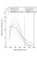
図4〜図7に、実施形態に係るBi含有率0.4〜32mol%の光電陰極のサンプル、Bi含有率0mol%であること以外は実施例と同じ構成とされた比較例に係る光電陰極のサンプル(比較例C2)、酸化マンガンを下地層としたバイアルカリ光電陰極の従来品のサンプル(比較例A1)、及びマルチアルカリ光電陰極のサンプル(比較例B)の分光感度特性を示す。図4はBi含有率0mol%、0.4mol%、0.9mol%、1.8mol%の光電陰極のサンプル、図5はBi含有率2.0mol%、2.1mol%、6.9mol%、8.8mol%の光電陰極のサンプル、図6はBi含有率10.5mol%、11.4mol%、11.7mol%、12mol%の光電陰極のサンプル、図7はBi含有率13mol%、16.7mol%、29mol%、32mol%の光電陰極のサンプルについて、それぞれの波長に対する量子効率を示すグラフである。図4〜図7に示すグラフの横軸は波長(nm)を、縦軸は量子効率(%)を示す。なお、図4〜7には、酸化マンガンを下地層としたバイアルカリ光電陰極の従来品のサンプル(比較例A1)、及びマルチアルカリ光電陰極のサンプル(比較例B)の分光感度特性がいずれも示されている。 4 to 7 show a photocathode sample having a Bi content of 0.4 to 32 mol% according to the embodiment, and a photocathode according to a comparative example having the same configuration as that of the example except that the Bi content is 0 mol%. The spectral sensitivity characteristics of a sample (Comparative Example C2), a conventional sample of a bialkali photocathode (Comparative Example A1) using manganese oxide as an underlayer, and a sample of a multialkali photocathode (Comparative Example B) are shown. 4 is a sample of a photocathode having a Bi content of 0 mol%, 0.4 mol%, 0.9 mol%, and 1.8 mol%, and FIG. 5 is a Bi content of 2.0 mol%, 2.1 mol%, 6.9 mol%, 8.8 mol% photocathode sample, FIG. 6 shows Bi content 10.5 mol%, 11.4 mol%, 11.7 mol%, 12 mol% photocathode sample, FIG. 7 shows Bi content 13 mol%, 16. It is a graph which shows the quantum efficiency with respect to each wavelength about the sample of 7 mol%, 29 mol%, and 32 mol% of a photocathode. 4 to 7, the horizontal axis represents wavelength (nm) and the vertical axis represents quantum efficiency (%). 4 to 7 show the spectral sensitivity characteristics of the bialkali photocathode sample (Comparative Example A1) and the multialkali photocathode sample (Comparative Example B), both of which have manganese oxide as an underlayer. It is shown.
図4及び図5から理解されるように、Bi含有率0.4mol%のサンプル(ZK4300)、Bi含有率0.9mol%のサンプル(ZK4295)、Bi含有率1.8mol%のサンプル(ZK4304)、Bi含有率2.0mol%のサンプル(ZK4293)、Bi含有率2.1mol%のサンプル(ZK4175)、Bi含有率6.9mol%のサンプル(ZK4152)は、波長300〜430nmでのピークにおいて35%以上の量子効率を示す。従って、光電子放出層18のSb及びBiに対して含有されるBiを6.9mol%以下とすることによって、特に感度を要求される分野において十分な感度とされている35%以上の量子効率を確保できることが理解される。なお、Bi含有率0mol%のサンプル(比較例C2)においても高い感度を確保できることが確認できるが、後述するように暗電流が大きくなってしまい、リニアリティも十分に得られない。
As understood from FIGS. 4 and 5, a sample with Bi content of 0.4 mol% (ZK4300), a sample with Bi content of 0.9 mol% (ZK4295), a sample with Bi content of 1.8 mol% (ZK4304) A sample with a Bi content of 2.0 mol% (ZK4293), a sample with a Bi content of 2.1 mol% (ZK4175), and a sample with a Bi content of 6.9 mol% (ZK4152) are 35 in the peak at a wavelength of 300 to 430 nm. % Quantum efficiency. Therefore, by setting Bi contained in Sb and Bi of the
図5〜7から理解されるように、Bi含有率8.8mol%のサンプル(ZK4305)、Bi含有率10.5mol%のサンプル(ZK4147)、Bi含有率11.4mol%のサンプル(ZK4004)、Bi含有率11.7mol%のサンプル(ZK4302)、Bi含有率12mol%のサンプル(ZK4298)、Bi含有率13mol%のサンプル(ZK4291)、Bi含有率16.7mol%のサンプル(ZK4142)は、波長300〜500nmの間のピークにおいて20%以上の量子効率を示すと共に、酸化マンガンを下地層としたバイアルカリ光電陰極の従来品のサンプル(比較例A1)よりも全ての波長において高い量子効率を示す。従って、光電子放出層にSbBiに対して含有されるBiを16.7mol%以下とすることによって、従来のバイアルカリ光電陰極よりも高い量子効率を確保できることが理解される。特に、Bi含有率を16.7mol%以下においては、波長500〜600nmにおいて従来品のサンプルよりも高い量子効率を示している。従って、光電子放出層のSbBiに対して16.7mol%以下のBiが含有されることによって、従来のバイアルカリ光電陰極よりも500〜600nmにおける感度、すなわち緑色感度〜赤感度を向上できることが理解される。 As understood from FIGS. 5 to 7, a sample with a Bi content of 8.8 mol% (ZK4305), a sample with a Bi content of 10.5 mol% (ZK4147), a sample with a Bi content of 11.4 mol% (ZK4004), A sample with a Bi content of 11.7 mol% (ZK4302), a sample with a Bi content of 12 mol% (ZK4298), a sample with a Bi content of 13 mol% (ZK4291), and a sample with a Bi content of 16.7 mol% (ZK4142) In addition to showing a quantum efficiency of 20% or more at a peak between 300 and 500 nm, the quantum efficiency is higher at all wavelengths than a conventional sample of a bialkali photocathode having a manganese oxide base layer (Comparative Example A1). . Therefore, it is understood that the quantum efficiency higher than that of the conventional bialkali photocathode can be secured by setting Bi contained in the photoelectron emission layer to 16.7 mol% or less. In particular, when the Bi content is 16.7 mol% or less, the quantum efficiency is higher than that of the conventional sample at a wavelength of 500 to 600 nm. Therefore, it is understood that the sensitivity at 500 to 600 nm, that is, the green sensitivity to the red sensitivity can be improved as compared with the conventional bialkali photocathode by containing 16.7 mol% or less of Bi with respect to SbBi of the photoelectron emission layer. The
図7から理解されるように、Bi含有率29mol%のサンプル(ZK4192)は、波長320〜440nmの間のピークにおいて20%以上の量子効率を示す。従って、光電子放出層にSbBiに対して29mol%以下のBiが含有されることによって、半導体検査装置などのように入射される光量が大きい分野において十分な感度とされている20%以上の量子効率を得ることができることが理解される。また、波長450〜500nmにおいて、マルチアルカリ光電陰極のサンプル(比較例B)より大きい、あるいは同等の量子効率を示す。 As understood from FIG. 7, the sample (ZK4192) having a Bi content of 29 mol% shows a quantum efficiency of 20% or more at a peak between wavelengths of 320 to 440 nm. Accordingly, a quantum efficiency of 20% or more, which is considered to be sufficient sensitivity in a field where the amount of incident light is large, such as a semiconductor inspection apparatus, by containing 29 mol% or less of Bi with respect to SbBi in the photoelectron emission layer. It is understood that can be obtained. Moreover, it shows a quantum efficiency larger than or equivalent to the sample of the multi-alkali photocathode (Comparative Example B) at a wavelength of 450 to 500 nm.
次に光電陰極のBi含有率ごとの陰極感度、陽極感度、暗電流、陰極青感度指数、及びダークカウントを比較した実験結果を表1に示す。表1においては、実施例に係る光電陰極として、Bi含有率0.4〜16.7mol%のサンプルの測定結果が示され、比較例に係る光電陰極として、酸化マンガンを下地層としたバイアルカリ光電陰極の従来品のサンプル(比較例A1)、及びBi含有率0mol%とされた光電陰極のサンプル(比較例C1,比較例D、比較例E)の測定結果が示されている。Bi含有率0.4〜16.7mol%のサンプル及びBi含有率0mol%とされた光電陰極のサンプル(比較例C1,比較例D、比較例E)は、いずれも基板12に形成された酸化ハフニウム(HfO2)からなる中間層14と、その上に形成されたMgOからなる下地層16とを有している。
Next, Table 1 shows the experimental results comparing the cathode sensitivity, anode sensitivity, dark current, cathode blue sensitivity index, and dark count for each Bi content of the photocathode. In Table 1, the measurement result of the sample of Bi content rate 0.4-16.7 mol% is shown as a photocathode which concerns on an Example, and the bialkali which used manganese oxide as a base layer as a photocathode which concerns on a comparative example The measurement results of the conventional sample of the photocathode (Comparative Example A1) and the photocathode sample (Comparative Example C1, Comparative Example D, and Comparative Example E) with a Bi content of 0 mol% are shown. Samples having a Bi content of 0.4 to 16.7 mol% and photocathode samples having a Bi content of 0 mol% (Comparative Example C1, Comparative Example D, and Comparative Example E) were both oxidized on the

表1における陰極青感度指数とは、ルーメン感度の測定時に青フィルタCS−5−58(コーニング社製)の1/2の厚みのフィルタを光電子増倍管30の前に入れたときの陰極電流(A/lm−b)である。
The cathode blue sensitivity index in Table 1 is the cathode current when a filter having a thickness of 1/2 of the blue filter CS-5-58 (manufactured by Corning) is put in front of the
表1におけるダークカウントとは、光電陰極10に入射する光を遮断した暗中状態において、光電子放出層18から放出される光電子の数を相対的に比較するための値で、25℃の室温環境下で測定を行ったものである。このダークカウントは、具体的には光電子をカウントする測定器によって得られる図8の結果に基づいて算出される。図8は、暗中状態において光電子放出層から放出される光電子の強度ごとのカウント数を示す図であり、Bi含有率0mol%(比較例C1)、2.1mol%、6.9mol%、10.5mol%、16,7mol%の光電陰極のサンプル、及び酸化マンガンを下地層とした従来品のサンプル(比較例A1)について示した図である。図8の横軸は測定器のチャンネルを示し、横軸は各チャンネルで検出された光電子のカウント数を示している。表1におけるダークカウントは、図8に示す光電子のカウント数のピークの1/3以上のチャンネルにおけるカウント数の積分値を示す。(具体的にはピークが200chなので、1/3は200/3=67チャンネルとなる)このように、ピークの1/3以上のチャンネルにおけるカント数の積分値を比較することによって、装置の回路内の揺らぎなどの影響を排除することができる。
The dark count in Table 1 is a value for relatively comparing the number of photoelectrons emitted from the
表1から理解されるように、酸化マンガンを下地層とした従来品のサンプル(比較例A1)については、暗電流及びダークカウントについて低い値が得られるものの十分な陰極青感度指数が得られない。実施例に係るBiを含有した光電陰極のサンプルでは、暗電流及びダークカウントについて低い値を得つつも比較例A1よりも高い陰極青感度を得ることができる。 As can be seen from Table 1, for the conventional sample (Comparative Example A1) with manganese oxide as the underlayer, a low value for dark current and dark count can be obtained, but a sufficient cathode blue sensitivity index cannot be obtained. . The photocathode sample containing Bi according to the example can obtain a higher cathode blue sensitivity than the comparative example A1 while obtaining low values for the dark current and the dark count.
表1に示されたダークカウントの値とBi含有率の関係を図9に示す。図9は、Bi含有率0.4〜16.7mol%の光電陰極のサンプル、及びBi含有率0mol%で中間層がHfO2とされた光電陰極のサンプル(比較例C1,比較例D,比較例E)のダークカウントの値をプロットしたグラフである。図9に示すグラフの横軸はBi含有率(mol%)を、縦軸はダークカウントの値を示す。 FIG. 9 shows the relationship between the dark count value shown in Table 1 and the Bi content. FIG. 9 shows a sample of a photocathode having a Bi content of 0.4 to 16.7 mol%, and a photocathode sample having a Bi content of 0 mol% and an intermediate layer of HfO 2 (Comparative Example C1, Comparative Example D, Comparison) It is the graph which plotted the value of the dark count of Example E). The horizontal axis of the graph shown in FIG. 9 indicates the Bi content (mol%), and the vertical axis indicates the dark count value.
図9から理解されるように、Bi含有率0mol%の光電陰極のサンプル(比較例C1,比較例D,比較例E)に比して、Bi含有率が0.4mol%以上の光電陰極のサンプルは、いずれもダークカウントの値が半分以上低減されている。なお、Bi含有率10.5mol%以上と16.7mol%以下の間の13mol%においても、ダークカウントの低減が見られた。 As understood from FIG. 9, the photocathode having a Bi content of 0.4 mol% or more as compared with the photocathode sample (Comparative Example C1, Comparative Example D, and Comparative Example E) having a Bi content of 0 mol%. In all the samples, the dark count value is reduced by more than half. In addition, the reduction of dark count was seen also in 13 mol% between Bi content rate 10.5 mol% or more and 16.7 mol% or less.
図9におけるBi含有率が低い領域におけるダークカウントの値とBi含有率の関係を図10に示す。図10は、Bi含有率0.4〜2.1mol%の光電陰極のサンプル、及びBi含有率0mol%で中間層がHfO2とされた光電陰極のサンプル(比較例C1,比較例D,比較例E)のダークカウントの値をプロットしたグラフである。図10に示すグラフの横軸はBi含有率(mol%)を、縦軸はダークカウントの値を示す。 FIG. 10 shows the relationship between the dark count value and the Bi content in the region where the Bi content is low in FIG. FIG. 10 shows a sample of a photocathode having a Bi content of 0.4 to 2.1 mol%, and a photocathode sample having a Bi content of 0 mol% and an intermediate layer of HfO 2 (Comparative Example C1, Comparative Example D, Comparison) It is the graph which plotted the value of the dark count of Example E). The horizontal axis of the graph shown in FIG. 10 indicates the Bi content (mol%), and the vertical axis indicates the dark count value.
図10から理解されるように、Bi含有率0.4mol%の光電陰極のサンプルは、Bi含有率0mol%の光電陰極のサンプル(比較例C1,比較例D,比較例E)に比してダークカウントが顕著に低減されている。従って、Biを微量でも含んでいれば、すなわちBi含有率が0mol%よりも大きければ、ダークカウントの値を低減するという効果を得られることが理解される。以上によって、SbにBiを含有させることによって、酸化マンガンを下地層とした従来品のサンプルよりも高い陰極青感度指数を得つつも(表1参照)、ダークカウントの値を低減できることが理解される。 As understood from FIG. 10, the photocathode sample having a Bi content of 0.4 mol% is compared with the photocathode samples having a Bi content of 0 mol% (Comparative Example C1, Comparative Example D, and Comparative Example E). The dark count is significantly reduced. Therefore, it is understood that if Bi is contained even in a small amount, that is, if the Bi content is larger than 0 mol%, the effect of reducing the dark count value can be obtained. From the above, it is understood that by adding Bi to Sb, the dark count value can be reduced while obtaining a higher cathode blue sensitivity index than that of the conventional sample using manganese oxide as an underlayer (see Table 1). The
図11及び図12に、Bi含有率2.0〜32mol%の光電陰極のサンプルのリニアリティを示す。図11はBi含有率2.0mol%、2.1mol%、6.9mol%、8.8mol%、10.5mol%、11.7mol%、12mol%、13.3mol%の光電陰極のサンプル、図12はBi含有率16.7mol%、29mol%、32mol%の光電陰極のサンプルについて、それぞれの陰極電流に対する変化率を示すグラフである。図11及び図12に示すグラフの横軸は陰極電流(A)を、縦軸は変化率(%)を示す。なお、定められた色温度を持つ光源の光束をミラーを介した測定系で、減光フィルターで1:4の光量に分割した基準光量をサンプルの光電陰極に入射して1:4の基準光電流値を変化率0%と定め、1:4の光量を増加させた場合の1:4の光電流の比率変化を変化率とする。図13は、図11及び図12に示されている変化率が−5%のときの陰極電流を各含有率についてプロットしたグラフである。図13の横軸はBiの含有率(mol%)を、縦軸は変化率−5%における陰極電流(A)を示す。なお、比較例A1,A2に係るバイアルカリ光電陰極(Sb−K−Cs)のリニアリティの上限値は0.01μAであることが知られているため、図13において1.0×10−8Aの位置を点線で示す。また、比較例Bに係るマルチアルカリ光電陰極(Sb−Na−K−Cs)のリニアリティの上限値は10μAであることが知られているため、図13において1.0×10−5Aの位置を一点鎖線で示す。 11 and 12 show the linearity of a sample of a photocathode having a Bi content of 2.0 to 32 mol%. FIG. 11 is a photocathode sample having a Bi content of 2.0 mol%, 2.1 mol%, 6.9 mol%, 8.8 mol%, 10.5 mol%, 11.7 mol%, 12 mol%, 13.3 mol%, 12 is a graph showing the rate of change with respect to the cathode current of each photocathode sample having a Bi content of 16.7 mol%, 29 mol%, and 32 mol%. 11 and 12, the horizontal axis represents the cathode current (A), and the vertical axis represents the rate of change (%). Note that a reference light amount obtained by dividing a light beam of a light source having a predetermined color temperature into a light amount of 1: 4 by a neutral density filter through a mirror is incident on a photocathode of a sample, and a reference light of 1: 4 is obtained. The current value is defined as a change rate of 0%, and the change in the ratio of the photocurrent of 1: 4 when the light amount of 1: 4 is increased is defined as the change rate. FIG. 13 is a graph in which the cathode current when the rate of change shown in FIGS. 11 and 12 is −5% is plotted for each content rate. The horizontal axis of FIG. 13 indicates the Bi content (mol%), and the vertical axis indicates the cathode current (A) at a change rate of −5%. In addition, since it is known that the upper limit of the linearity of the bialkali photocathode (Sb-K-Cs) according to Comparative Examples A1 and A2 is 0.01 μA, 1.0 × 10 −8 A in FIG. Is indicated by a dotted line. Moreover, since it is known that the upper limit of the linearity of the multi-alkali photocathode (Sb—Na—K—Cs) according to Comparative Example B is 10 μA, the position of 1.0 × 10 −5 A in FIG. Is shown by a one-dot chain line.
図13から理解されるように、Bi含有率8.8mol%以上のサンプルでは、マルチアルカリ光電陰極のリニアリティの上限値(1.0×10⁻⁵A)と同等のリニアリティを示す。また、8.8mol%よりBi含有率が低い光電陰極においては、Bi含有率の変化に対するリニアリティの変化が大きく、Bi含有率の低下によってリニアリティが大幅に減少するのに対し、Bi含有率が8.8mol%以上の光電陰極においては、Bi含有率の変化に対するリニアリティの変化が少ない。従って、製造誤差によってBi含有率が若干変化した場合であっても、リニアリティが急激に変化することなく、高いリニアリティを安定して確保することができる。以上によって、光電子放出層18のSbBiに対して8.8mol%以上のBiが含有されることによって、マルチアルカリ光電陰極のリニアリティの上限値とほぼ同等のリニアリティを安定して得ることができる。
As understood from FIG. 13, a sample having a Bi content of 8.8 mol% or more shows a linearity equivalent to the upper limit (1.0 × 10 −5 A) of the linearity of the multi-alkali photocathode. Further, in the photocathode having a Bi content lower than 8.8 mol%, the change in linearity with respect to the change in Bi content is large, and the linearity is greatly reduced due to the decrease in Bi content, whereas the Bi content is 8 In a photocathode of .8 mol% or more, the change in linearity with respect to the change in Bi content is small. Therefore, even if the Bi content is slightly changed due to a manufacturing error, high linearity can be stably secured without abrupt change in linearity. As described above, when 8.8 mol% or more of Bi is contained with respect to SbBi of the
図14は、変化率が−5%のときの陰極電流を各含有率について温度ごとにプロットしたグラフであり、実施例に係るBi含有率32mol%の光電陰極のサンプル(ZK4198)、Bi含有率16.7mol%の光電陰極のサンプル(ZK4142)、及び比較例に係る酸化マンガンを下地層としたバイアルカリ光電陰極の従来品のサンプル(比較例A2)について、低温環境下でリニアリティの測定を行った場合の測定結果を示している。図14の横軸は測定環境における温度(℃)を、縦軸は変化率−5%における陰極電流(A)を示す。 FIG. 14 is a graph in which the cathode current when the rate of change is −5% is plotted for each content rate for each temperature. A photocathode sample (ZK4198) with a Bi content rate of 32 mol% according to the example, Bi content rate The linearity of a 16.7 mol% photocathode sample (ZK4142) and a conventional bialkali photocathode sample (Comparative Example A2) based on manganese oxide according to a comparative example were measured in a low temperature environment. The measurement results are shown. The horizontal axis in FIG. 14 indicates the temperature (° C.) in the measurement environment, and the vertical axis indicates the cathode current (A) at a change rate of −5%.
図14から理解されるように、酸化マンガンを下地層としたバイアルカリ光電陰極の従来品のサンプル(比較例A2)は、温度低下に伴って急激にリニアリティが低下しており、−100℃におけるリニアリティが室温(25℃)におけるリニアリティに比して1×10−4倍以上低下している。一方、Bi含有率16.7mol%のサンプル(ZK4142)については、―100℃におけるリニアリティが室温(25℃)におけるリニアリティに比して0.1倍しか低下していない。また、Bi含有率32mol%のサンプル(ZK4198)については、―100℃におけるリニアリティが室温におけるリニアリティに比してほとんど低下していない。従って、Bi含有率を32mol%以下とすることによって、低温時におけるリニアリティを飛躍的に向上できることが理解される。このように低温時におけるリニアリティを向上させることのできる光電陰極は、例えば、高エネルギー物理学者により行われる宇宙の暗黒物質(ダークマター)の観測などに用いるのに好適である。この観測には、液体アルゴンシンチレータ(-189℃)、液体キセノンシンチレータ(-112℃)が用いられる。図14で示す様に従来の比較例A2では、−100℃の環境でのカソード電流がわずか1.0×10−11(A)しか流れなくなり,測定ができなかった。液体キセノンシンチレータを使用する場合は、ZK4142(Bi=16.7mol%)、液体アルゴンシンチレータ使用の場合はZK4198(Bi=32mol%)を用いることが望ましい。 As understood from FIG. 14, the sample of the conventional product of the bialkali photocathode having the manganese oxide as the underlayer (Comparative Example A2) has drastically reduced linearity as the temperature decreased, and at −100 ° C. The linearity is 1 × 10 −4 times or more lower than the linearity at room temperature (25 ° C.). On the other hand, for the sample (ZK4142) having a Bi content of 16.7 mol%, the linearity at −100 ° C. is only 0.1 times lower than the linearity at room temperature (25 ° C.). Further, in the sample (ZK4198) having a Bi content of 32 mol%, the linearity at −100 ° C. is hardly lowered as compared with the linearity at room temperature. Therefore, it is understood that the linearity at low temperatures can be drastically improved by setting the Bi content to 32 mol% or less. Thus, the photocathode capable of improving the linearity at low temperatures is suitable for use in, for example, observation of dark matter in the universe performed by a high energy physicist. For this observation, a liquid argon scintillator (−189 ° C.) and a liquid xenon scintillator (−112 ° C.) are used. As shown in FIG. 14, in the comparative example A2 of the related art, only 1.0 × 10 −11 (A) of the cathode current in an environment of −100 ° C. flowed and measurement was not possible. When using a liquid xenon scintillator, it is desirable to use ZK4142 (Bi = 16.7 mol%), and when using a liquid argon scintillator, ZK4198 (Bi = 32 mol%).
以上、好適な実施形態について説明したが、上記実施形態に限定されるものではなく、様々な変形が可能である。例えば、光電陰極10において、基板12、下地層16に含まれる物質は上記に記載した物質に限定されない。また、中間層14を設けなくともよい。光電陰極の各層を形成する方法は、それぞれ上記実施形態に記載された方法に限られない。
As mentioned above, although preferred embodiment was described, it is not limited to the said embodiment, A various deformation | transformation is possible. For example, in the
また、光電子増倍管以外にイメージインテンシファイア(II管)などの電子管に本実施形態に係る光電陰極を適用してもよい。NaIシンチレータと光電陰極を組み合わせることによって、微弱X線と強いX線の識別ができるため、コントラストの良い画像が得られる。 In addition to the photomultiplier tube, the photocathode according to this embodiment may be applied to an electron tube such as an image intensifier (II tube). By combining a NaI scintillator and a photocathode, weak X-rays and strong X-rays can be distinguished, and an image with good contrast can be obtained.
また、イメージインテンシファイア(高速シャッター管)の実施形態において本光電陰極を用いることにより、光電陰極の抵抗が従来品より小さいため、特別の導電下地(金属Niなど)を用いなくても、高感度で、より高速シャッターが可能となる。 Further, by using the present photocathode in the embodiment of the image intensifier (high-speed shutter tube), the resistance of the photocathode is smaller than that of the conventional product. Sensitivity enables higher shutter speeds.
10…光電陰極、12…基板、14…中間層、16…下地層、18…光電子放出層。
DESCRIPTION OF
Claims (3)
前記光電子放出層の光の入射側に形成される、光透過性の基板と、
前記光電子放出層の光の入射側に、前記基板と前記光電子放出層との間に形成される、MgOから形成される下地層と、を備え、
前記基板上には、前記下地層が形成され、又はHfO2から形成される中間層を介して前記下地層が形成され、
前記下地層上には、前記光電子放出層が形成され、
前記光電子放出層には、Sb及びBiに対して0.4mol%以上、6.9mol%以下のBiが含有されていることを特徴とする光電陰極。 A photoelectron emission layer containing Sb and Bi and emitting photoelectrons to the outside by the incidence of light;
A light transmissive substrate formed on the light incident side of the photoelectron emitting layer;
An underlayer formed of MgO formed between the substrate and the photoelectron emission layer on the light incident side of the photoelectron emission layer;
On the substrate, the base layer is formed, or the base layer is formed through an intermediate layer formed of HfO 2 ,
The photoelectron emission layer is formed on the underlayer,
The photoelectron emission layer contains 0.4 mol% or more and 6.9 mol% or less of Bi with respect to Sb and Bi.
Priority Applications (8)
| Application Number | Priority Date | Filing Date | Title |
|---|---|---|---|
| JP2008155777A JP5308078B2 (en) | 2008-06-13 | 2008-06-13 | Photocathode |
| PCT/JP2008/070329 WO2009150760A1 (en) | 2008-06-13 | 2008-11-07 | Photocathode |
| CN200880129779.XA CN102067264B (en) | 2008-06-13 | 2008-11-07 | Photocathode |
| EP17194401.0A EP3288060A1 (en) | 2008-06-13 | 2008-11-07 | Photocathode |
| CN201610216950.7A CN105788997B (en) | 2008-06-13 | 2008-11-07 | Photocathode |
| US12/996,526 US8796923B2 (en) | 2008-06-13 | 2008-11-07 | Photocathode |
| EP08874613.6A EP2309529B1 (en) | 2008-06-13 | 2008-11-07 | Photocathode |
| CN201410085728.9A CN103887126B (en) | 2008-06-13 | 2008-11-07 | Photocathode |
Applications Claiming Priority (1)
| Application Number | Priority Date | Filing Date | Title |
|---|---|---|---|
| JP2008155777A JP5308078B2 (en) | 2008-06-13 | 2008-06-13 | Photocathode |
Related Child Applications (1)
| Application Number | Title | Priority Date | Filing Date |
|---|---|---|---|
| JP2012204735A Division JP5955713B2 (en) | 2012-09-18 | 2012-09-18 | Photocathode |
Publications (2)
| Publication Number | Publication Date |
|---|---|
| JP2009301905A JP2009301905A (en) | 2009-12-24 |
| JP5308078B2 true JP5308078B2 (en) | 2013-10-09 |
Family
ID=41416479
Family Applications (1)
| Application Number | Title | Priority Date | Filing Date |
|---|---|---|---|
| JP2008155777A Active JP5308078B2 (en) | 2008-06-13 | 2008-06-13 | Photocathode |
Country Status (5)
| Country | Link |
|---|---|
| US (1) | US8796923B2 (en) |
| EP (2) | EP2309529B1 (en) |
| JP (1) | JP5308078B2 (en) |
| CN (3) | CN103887126B (en) |
| WO (1) | WO2009150760A1 (en) |
Families Citing this family (7)
| Publication number | Priority date | Publication date | Assignee | Title |
|---|---|---|---|---|
| JP5899187B2 (en) | 2013-11-01 | 2016-04-06 | 浜松ホトニクス株式会社 | Transmission type photocathode |
| JP6419572B2 (en) * | 2014-12-26 | 2018-11-07 | 浜松ホトニクス株式会社 | Photocathode, photoelectric conversion tube, image intensifier, and photomultiplier tube |
| GB2556289A (en) | 2015-09-14 | 2018-05-23 | Halliburton Energy Services Inc | Dark current correction in scintillator detectors for downhole nuclear applications |
| CN111448481A (en) * | 2017-12-11 | 2020-07-24 | 拉皮斯坎系统股份有限公司 | X-ray tomography inspection system and method |
| CN110783157B (en) * | 2019-10-24 | 2021-11-05 | 北方夜视技术股份有限公司 | Composite optical film applied to multi-alkali photoelectric cathode and preparation method thereof |
| CN111816533B (en) * | 2019-11-13 | 2022-03-25 | 北方夜视技术股份有限公司 | Double-alkali photoelectric cathode and preparation method thereof |
| CN111261472B (en) * | 2020-03-31 | 2022-03-25 | 北方夜视技术股份有限公司 | Low-thermal-emission photocathode, photomultiplier and preparation method thereof |
Family Cites Families (9)
| Publication number | Priority date | Publication date | Assignee | Title |
|---|---|---|---|---|
| US2645721A (en) * | 1952-02-16 | 1953-07-14 | Gen Electric | Image intensification apparatus |
| NL233704A (en) * | 1957-12-06 | |||
| JPS52105766A (en) * | 1976-03-03 | 1977-09-05 | Hamamatsu Tv Co Ltd | Photoelectron emitting surface |
| FR2515870A1 (en) * | 1981-11-04 | 1983-05-06 | Labo Electronique Physique | PHOTOCATHODE FOR ELECTRONIC TUBE ENTRY COMPRISING A SEMICONDUCTOR DEVICE WITH TRANSMISSION PHOTO-EMISSION |
| JP3179537B2 (en) | 1991-11-19 | 2001-06-25 | 浜松ホトニクス株式会社 | Photocathode and photomultiplier tube |
| US6770884B2 (en) | 2002-07-11 | 2004-08-03 | Triumf | High resolution 3-D position sensitive detector for gamma rays |
| WO2005096403A2 (en) * | 2004-03-31 | 2005-10-13 | Matsushita Electric Industrial Co., Ltd. | Organic photoelectric conversion element utilizing an inorganic buffer layer placed between an electrode and the active material |
| KR100647305B1 (en) | 2004-12-23 | 2006-11-23 | 삼성에스디아이 주식회사 | Optoelectronic device and lamp and display panel using same |
| JP4926504B2 (en) * | 2006-03-08 | 2012-05-09 | 浜松ホトニクス株式会社 | Photocathode, electron tube provided with the photocathode, and method for producing photocathode |
-
2008
- 2008-06-13 JP JP2008155777A patent/JP5308078B2/en active Active
- 2008-11-07 CN CN201410085728.9A patent/CN103887126B/en active Active
- 2008-11-07 EP EP08874613.6A patent/EP2309529B1/en active Active
- 2008-11-07 CN CN200880129779.XA patent/CN102067264B/en active Active
- 2008-11-07 US US12/996,526 patent/US8796923B2/en active Active
- 2008-11-07 CN CN201610216950.7A patent/CN105788997B/en active Active
- 2008-11-07 EP EP17194401.0A patent/EP3288060A1/en active Pending
- 2008-11-07 WO PCT/JP2008/070329 patent/WO2009150760A1/en active Application Filing
Also Published As
| Publication number | Publication date |
|---|---|
| WO2009150760A1 (en) | 2009-12-17 |
| JP2009301905A (en) | 2009-12-24 |
| EP3288060A1 (en) | 2018-02-28 |
| EP2309529B1 (en) | 2017-10-04 |
| CN105788997B (en) | 2018-10-19 |
| US8796923B2 (en) | 2014-08-05 |
| EP2309529A4 (en) | 2015-06-03 |
| CN103887126A (en) | 2014-06-25 |
| EP2309529A1 (en) | 2011-04-13 |
| US20110089825A1 (en) | 2011-04-21 |
| CN105788997A (en) | 2016-07-20 |
| CN102067264B (en) | 2014-07-02 |
| CN103887126B (en) | 2017-06-20 |
| CN102067264A (en) | 2011-05-18 |
Similar Documents
| Publication | Publication Date | Title |
|---|---|---|
| JP5308078B2 (en) | Photocathode | |
| US8421354B2 (en) | Photocathode, photomultiplier and electron tube | |
| US5982094A (en) | Electron tube with polycrystalline diamond photocathode | |
| JP4926504B2 (en) | Photocathode, electron tube provided with the photocathode, and method for producing photocathode | |
| JP5955713B2 (en) | Photocathode | |
| JP6419572B2 (en) | Photocathode, photoelectric conversion tube, image intensifier, and photomultiplier tube | |
| EP0532358B1 (en) | Reflection type photocathode and photomultiplier using it | |
| JP4562844B2 (en) | Photocathode and electron tube | |
| JP5865527B2 (en) | Photocathode and photomultiplier tube | |
| US5463272A (en) | Cathode for photoelectric emission, cathode for secondary electron emission, electron multiplier tube, and photomultiplier tube | |
| JP2014044960A (en) | Photocathode | |
| JP3642664B2 (en) | Photocathode and electron tube having the same | |
| RU2558387C1 (en) | Electro-optical display and method of making same | |
| JPH11120899A (en) | Secondary electron discharge device and electron tube using the device |
Legal Events
| Date | Code | Title | Description |
|---|---|---|---|
| A621 | Written request for application examination |
Free format text: JAPANESE INTERMEDIATE CODE: A621 Effective date: 20110606 |
|
| A131 | Notification of reasons for refusal |
Free format text: JAPANESE INTERMEDIATE CODE: A131 Effective date: 20120717 |
|
| A521 | Request for written amendment filed |
Free format text: JAPANESE INTERMEDIATE CODE: A523 Effective date: 20120918 |
|
| A131 | Notification of reasons for refusal |
Free format text: JAPANESE INTERMEDIATE CODE: A131 Effective date: 20130326 |
|
| A521 | Request for written amendment filed |
Free format text: JAPANESE INTERMEDIATE CODE: A523 Effective date: 20130520 |
|
| TRDD | Decision of grant or rejection written | ||
| A01 | Written decision to grant a patent or to grant a registration (utility model) |
Free format text: JAPANESE INTERMEDIATE CODE: A01 Effective date: 20130604 |
|
| A61 | First payment of annual fees (during grant procedure) |
Free format text: JAPANESE INTERMEDIATE CODE: A61 Effective date: 20130628 |
|
| R150 | Certificate of patent or registration of utility model |
Free format text: JAPANESE INTERMEDIATE CODE: R150 Ref document number: 5308078 Country of ref document: JP Free format text: JAPANESE INTERMEDIATE CODE: R150 |
|
| R250 | Receipt of annual fees |
Free format text: JAPANESE INTERMEDIATE CODE: R250 |