JP5295259B2 - Pre-aligner device - Google Patents
Pre-aligner device Download PDFInfo
- Publication number
- JP5295259B2 JP5295259B2 JP2010534627A JP2010534627A JP5295259B2 JP 5295259 B2 JP5295259 B2 JP 5295259B2 JP 2010534627 A JP2010534627 A JP 2010534627A JP 2010534627 A JP2010534627 A JP 2010534627A JP 5295259 B2 JP5295259 B2 JP 5295259B2
- Authority
- JP
- Japan
- Prior art keywords
- wafer
- pair
- held
- transfer mechanism
- rotating
- Prior art date
- Legal status (The legal status is an assumption and is not a legal conclusion. Google has not performed a legal analysis and makes no representation as to the accuracy of the status listed.)
- Active
Links
- 238000001514 detection method Methods 0.000 claims description 18
- 239000004065 semiconductor Substances 0.000 claims description 9
- 235000012431 wafers Nutrition 0.000 description 131
- 230000009977 dual effect Effects 0.000 description 2
- 238000000034 method Methods 0.000 description 2
- 238000000926 separation method Methods 0.000 description 2
- 239000000758 substrate Substances 0.000 description 2
- 230000015572 biosynthetic process Effects 0.000 description 1
- 230000000694 effects Effects 0.000 description 1
- 238000005530 etching Methods 0.000 description 1
- 238000003384 imaging method Methods 0.000 description 1
- 238000004519 manufacturing process Methods 0.000 description 1
- 238000012986 modification Methods 0.000 description 1
- 230000004048 modification Effects 0.000 description 1
- 230000003287 optical effect Effects 0.000 description 1
- 230000002093 peripheral effect Effects 0.000 description 1
Images


Classifications
-
- H—ELECTRICITY
- H01—ELECTRIC ELEMENTS
- H01L—SEMICONDUCTOR DEVICES NOT COVERED BY CLASS H10
- H01L21/00—Processes or apparatus adapted for the manufacture or treatment of semiconductor or solid state devices or of parts thereof
- H01L21/67—Apparatus specially adapted for handling semiconductor or electric solid state devices during manufacture or treatment thereof; Apparatus specially adapted for handling wafers during manufacture or treatment of semiconductor or electric solid state devices or components ; Apparatus not specifically provided for elsewhere
- H01L21/67005—Apparatus not specifically provided for elsewhere
- H01L21/67242—Apparatus for monitoring, sorting or marking
- H01L21/67259—Position monitoring, e.g. misposition detection or presence detection
-
- H—ELECTRICITY
- H01—ELECTRIC ELEMENTS
- H01L—SEMICONDUCTOR DEVICES NOT COVERED BY CLASS H10
- H01L21/00—Processes or apparatus adapted for the manufacture or treatment of semiconductor or solid state devices or of parts thereof
- H01L21/67—Apparatus specially adapted for handling semiconductor or electric solid state devices during manufacture or treatment thereof; Apparatus specially adapted for handling wafers during manufacture or treatment of semiconductor or electric solid state devices or components ; Apparatus not specifically provided for elsewhere
- H01L21/677—Apparatus specially adapted for handling semiconductor or electric solid state devices during manufacture or treatment thereof; Apparatus specially adapted for handling wafers during manufacture or treatment of semiconductor or electric solid state devices or components ; Apparatus not specifically provided for elsewhere for conveying, e.g. between different workstations
- H01L21/67739—Apparatus specially adapted for handling semiconductor or electric solid state devices during manufacture or treatment thereof; Apparatus specially adapted for handling wafers during manufacture or treatment of semiconductor or electric solid state devices or components ; Apparatus not specifically provided for elsewhere for conveying, e.g. between different workstations into and out of processing chamber
- H01L21/67742—Mechanical parts of transfer devices
-
- H—ELECTRICITY
- H01—ELECTRIC ELEMENTS
- H01L—SEMICONDUCTOR DEVICES NOT COVERED BY CLASS H10
- H01L21/00—Processes or apparatus adapted for the manufacture or treatment of semiconductor or solid state devices or of parts thereof
- H01L21/67—Apparatus specially adapted for handling semiconductor or electric solid state devices during manufacture or treatment thereof; Apparatus specially adapted for handling wafers during manufacture or treatment of semiconductor or electric solid state devices or components ; Apparatus not specifically provided for elsewhere
- H01L21/677—Apparatus specially adapted for handling semiconductor or electric solid state devices during manufacture or treatment thereof; Apparatus specially adapted for handling wafers during manufacture or treatment of semiconductor or electric solid state devices or components ; Apparatus not specifically provided for elsewhere for conveying, e.g. between different workstations
- H01L21/67739—Apparatus specially adapted for handling semiconductor or electric solid state devices during manufacture or treatment thereof; Apparatus specially adapted for handling wafers during manufacture or treatment of semiconductor or electric solid state devices or components ; Apparatus not specifically provided for elsewhere for conveying, e.g. between different workstations into and out of processing chamber
- H01L21/67748—Apparatus specially adapted for handling semiconductor or electric solid state devices during manufacture or treatment thereof; Apparatus specially adapted for handling wafers during manufacture or treatment of semiconductor or electric solid state devices or components ; Apparatus not specifically provided for elsewhere for conveying, e.g. between different workstations into and out of processing chamber horizontal transfer of a single workpiece
-
- H—ELECTRICITY
- H01—ELECTRIC ELEMENTS
- H01L—SEMICONDUCTOR DEVICES NOT COVERED BY CLASS H10
- H01L21/00—Processes or apparatus adapted for the manufacture or treatment of semiconductor or solid state devices or of parts thereof
- H01L21/67—Apparatus specially adapted for handling semiconductor or electric solid state devices during manufacture or treatment thereof; Apparatus specially adapted for handling wafers during manufacture or treatment of semiconductor or electric solid state devices or components ; Apparatus not specifically provided for elsewhere
- H01L21/68—Apparatus specially adapted for handling semiconductor or electric solid state devices during manufacture or treatment thereof; Apparatus specially adapted for handling wafers during manufacture or treatment of semiconductor or electric solid state devices or components ; Apparatus not specifically provided for elsewhere for positioning, orientation or alignment
- H01L21/681—Apparatus specially adapted for handling semiconductor or electric solid state devices during manufacture or treatment thereof; Apparatus specially adapted for handling wafers during manufacture or treatment of semiconductor or electric solid state devices or components ; Apparatus not specifically provided for elsewhere for positioning, orientation or alignment using optical controlling means
-
- H—ELECTRICITY
- H01—ELECTRIC ELEMENTS
- H01L—SEMICONDUCTOR DEVICES NOT COVERED BY CLASS H10
- H01L21/00—Processes or apparatus adapted for the manufacture or treatment of semiconductor or solid state devices or of parts thereof
- H01L21/67—Apparatus specially adapted for handling semiconductor or electric solid state devices during manufacture or treatment thereof; Apparatus specially adapted for handling wafers during manufacture or treatment of semiconductor or electric solid state devices or components ; Apparatus not specifically provided for elsewhere
- H01L21/683—Apparatus specially adapted for handling semiconductor or electric solid state devices during manufacture or treatment thereof; Apparatus specially adapted for handling wafers during manufacture or treatment of semiconductor or electric solid state devices or components ; Apparatus not specifically provided for elsewhere for supporting or gripping
- H01L21/687—Apparatus specially adapted for handling semiconductor or electric solid state devices during manufacture or treatment thereof; Apparatus specially adapted for handling wafers during manufacture or treatment of semiconductor or electric solid state devices or components ; Apparatus not specifically provided for elsewhere for supporting or gripping using mechanical means, e.g. chucks, clamps or pinches
- H01L21/68707—Apparatus specially adapted for handling semiconductor or electric solid state devices during manufacture or treatment thereof; Apparatus specially adapted for handling wafers during manufacture or treatment of semiconductor or electric solid state devices or components ; Apparatus not specifically provided for elsewhere for supporting or gripping using mechanical means, e.g. chucks, clamps or pinches the wafers being placed on a robot blade, or gripped by a gripper for conveyance
-
- H—ELECTRICITY
- H01—ELECTRIC ELEMENTS
- H01L—SEMICONDUCTOR DEVICES NOT COVERED BY CLASS H10
- H01L21/00—Processes or apparatus adapted for the manufacture or treatment of semiconductor or solid state devices or of parts thereof
- H01L21/67—Apparatus specially adapted for handling semiconductor or electric solid state devices during manufacture or treatment thereof; Apparatus specially adapted for handling wafers during manufacture or treatment of semiconductor or electric solid state devices or components ; Apparatus not specifically provided for elsewhere
- H01L21/683—Apparatus specially adapted for handling semiconductor or electric solid state devices during manufacture or treatment thereof; Apparatus specially adapted for handling wafers during manufacture or treatment of semiconductor or electric solid state devices or components ; Apparatus not specifically provided for elsewhere for supporting or gripping
- H01L21/687—Apparatus specially adapted for handling semiconductor or electric solid state devices during manufacture or treatment thereof; Apparatus specially adapted for handling wafers during manufacture or treatment of semiconductor or electric solid state devices or components ; Apparatus not specifically provided for elsewhere for supporting or gripping using mechanical means, e.g. chucks, clamps or pinches
- H01L21/68714—Apparatus specially adapted for handling semiconductor or electric solid state devices during manufacture or treatment thereof; Apparatus specially adapted for handling wafers during manufacture or treatment of semiconductor or electric solid state devices or components ; Apparatus not specifically provided for elsewhere for supporting or gripping using mechanical means, e.g. chucks, clamps or pinches the wafers being placed on a susceptor, stage or support
- H01L21/68742—Apparatus specially adapted for handling semiconductor or electric solid state devices during manufacture or treatment thereof; Apparatus specially adapted for handling wafers during manufacture or treatment of semiconductor or electric solid state devices or components ; Apparatus not specifically provided for elsewhere for supporting or gripping using mechanical means, e.g. chucks, clamps or pinches the wafers being placed on a susceptor, stage or support characterised by a lifting arrangement, e.g. lift pins
Landscapes
- Engineering & Computer Science (AREA)
- Physics & Mathematics (AREA)
- Condensed Matter Physics & Semiconductors (AREA)
- General Physics & Mathematics (AREA)
- Manufacturing & Machinery (AREA)
- Computer Hardware Design (AREA)
- Microelectronics & Electronic Packaging (AREA)
- Power Engineering (AREA)
- Robotics (AREA)
- Container, Conveyance, Adherence, Positioning, Of Wafer (AREA)
Description
本発明は、基板処理装置での処理に先だって半導体ウェハを位置合わせするためのプリアライナー装置に関する。 The present invention relates to a pre-aligner apparatus for aligning a semiconductor wafer prior to processing in a substrate processing apparatus.
成膜装置、エッチング装置等の基板処理装置で半導体ウェハを処理する際には、半導体ウェハの周縁部に予め形成された位置決め用の切欠き部(ノッチ又はオリフラ)を基準として、半導体ウェハの位置合わせが行われる。 When a semiconductor wafer is processed by a substrate processing apparatus such as a film formation apparatus or an etching apparatus, the position of the semiconductor wafer is determined based on a positioning notch (notch or orientation flat) formed in advance on the peripheral edge of the semiconductor wafer. Matching is done.
この位置合わせを行うための装置はプリアライナー装置と呼ばれ、基本的な構成として、ウェハを保持して回転させる回転機構と、ウェハの切欠き部を検出する検出機構と、を備えている(特許文献1,2,3)。
An apparatus for performing this alignment is called a pre-aligner apparatus, and as a basic configuration, includes a rotation mechanism that holds and rotates a wafer, and a detection mechanism that detects a notch in the wafer (
プリアライナー装置へのウェハの受け渡しは例えばロボットによって行われ、このウェハ搬送用のロボットは、そのアームの先端にウェハを保持し得るハンドを備えている。 Transfer of the wafer to the pre-aligner apparatus is performed by a robot, for example, and the robot for wafer transfer includes a hand that can hold the wafer at the tip of its arm.
ロボットによってカセットから取り出されたウェハは、プリアライナー装置の回転機構の載置部の上に載置されてそこに保持され、回転機構によってウェハを回転させながら、検出機構によってウェハの切欠き部を検出する。このようにしてウェハのXY位置及び回転方向(θ方向)位置が検出されるが、この検出には一般的に3−10秒程度を要する。 The wafer taken out from the cassette by the robot is placed on the placement part of the rotation mechanism of the pre-aligner device and held there, and the wafer is notched by the detection mechanism while the wafer is rotated by the rotation mechanism. To detect. In this way, the XY position and rotation direction (θ direction) position of the wafer are detected, but this detection generally requires about 3-10 seconds.
近年、ウェハ処理のスループットをあげるために、このプリアライナー装置での位置合わせ作業に伴って必要となる作業時間が問題となっている。 In recent years, in order to increase the throughput of wafer processing, the working time required for the alignment work in this pre-aligner apparatus has become a problem.
そこで従来は、例えば、ウェハを搬送するロボットのアームを二本設けて、位置合わせ終了後のウェハを一方のアームによって回転機構から取り出したら、直ちに他方のアームで次のウェハをプリアライナー装置に搬入するという方法が取られていた。 Therefore, conventionally, for example, two robot arms for carrying a wafer are provided, and after positioning is completed, the wafer is taken out from the rotating mechanism by one arm, and the next wafer is immediately carried into the pre-aligner device by the other arm. The method of doing was taken.
このようにすれば、一本のアームによってプリアライナー装置からウェハを出し入れする場合に比べて、作業時間を全体として短縮することができる。 In this way, the work time as a whole can be shortened as compared with the case where the wafer is taken in and out from the pre-aligner apparatus with one arm.
[特許文献1] 日本国・特開2007−281249号公報
[特許文献2] 日本国・特開2004−363218号公報
[特許文献3] 日本国・特表2005−536878号公報
しかしながら、ロボットのアームを1本から2本に変更するためには多大のコストを必要とするため、ウェハ処理のスループットをあげることができたとしても、アームの2本化(デュアルアーム化)に伴うコスト上昇により、製造コストの低減効果が相殺されてしまうという問題があった。[Patent Document 1] Japan, JP 2007-281249 A [Patent Document 2] Japan, JP 2004-363218 A [Patent Document 3] Japan, JP 2005-536878 A However, a robot arm Since changing the cost from 1 to 2 requires a great deal of cost, even if the wafer processing throughput could be increased, the cost increase associated with the dual arming (dual arming) There was a problem that the effect of reducing the manufacturing cost was offset.
本発明は、上述した事情に鑑みてなされたものであって、多大なコスト上昇をもたらすことなく、ウェハ処理のスループットをあげることができるプリアライナー装置を提供することを目的とする。 The present invention has been made in view of the above-described circumstances, and an object of the present invention is to provide a pre-aligner apparatus that can increase the throughput of wafer processing without causing a significant cost increase.
上記課題を解決するために、本発明によるプリアライナー装置は、半導体ウェハを保持して回転させるための回転機構と、前記ウェハに形成された位置決め用切欠き部を検出するための検出機構と、前記回転機構のウェハ載置部から前記ウェハを持ち上げ又は前記ウェハ載置部にウェハを載置するためのウェハ移送機構と、を備え、前記ウェハ移送機構は、前記ウェハ載置部の直上位置で前記ウェハを保持するための一対の細長部材を有し、前記一対の細長部材は、前記ウェハと平行な共通の平面において延びており、前記ウェハ移送機構は、前記回転機構に保持されているウェハを迂回して前記一対の細長部材が前記回転機構に保持されているウェハの上方位置から前記回転機構に保持されているウェハの下方位置に、またはその逆に、移動するように構成されていることを特徴とする。 In order to solve the above problems, the pre-aligner apparatus according to the present invention includes a detection mechanism for detecting a rotation mechanism and, notch for positioning formed on the wafer for holding and rotating the semiconductors wafers A wafer transfer mechanism for lifting the wafer from the wafer mounting portion of the rotating mechanism or mounting the wafer on the wafer mounting portion, and the wafer transfer mechanism is located immediately above the wafer mounting portion. A pair of elongated members for holding the wafer, the pair of elongated members extending in a common plane parallel to the wafer, and the wafer transfer mechanism is held by the rotating mechanism bypassing the wafer at a lower position of the wafer in which the pair of elongate members is held from the upper position of the wafer held on the rotating mechanism in the rotation mechanism, or vice versa, shifting Characterized in that it is configured to.
上記課題を解決するために、本発明によるプリアライナー装置は、半導体ウェハを保持して回転させるための回転機構と、前記ウェハに形成された位置決め用切欠き部を検出するための検出機構と、前記回転機構のウェハ載置部から前記ウェハを持ち上げるためのウェハ移送機構と、を備え、前記ウェハ移送機構は、前記ウェハを持ち上げる際に上昇して前記ウェハの裏面に当接される一対の細長部材を有し、前記一対の細長部材は、前記ウェハと平行な共通の平面において延びており、前記ウェハ移送機構は、前記一対の細長部材により持ち上げられた前記ウェハが搬出された後、前記回転機構に保持されている次のウェハを迂回して前記一対の細長部材が前記回転機構に保持されているウェハの上方位置から前記回転機構に保持されているウェハの下方位置に、またはその逆に、移動するように構成されていることを特徴とする。 In order to solve the above problems, a pre-aligner device according to the present invention includes a rotation mechanism for holding and rotating a semiconductor wafer, a detection mechanism for detecting a positioning notch formed in the wafer, and a wafer transfer mechanism for lifting the wafer from the wafer mounting portion of the rotary mechanism, the wafer transfer mechanism, the pair that is in contact with the back surface of the wafer rises to lift the wafer elongated The pair of elongate members extend in a common plane parallel to the wafer, and the wafer transfer mechanism rotates the rotation after the wafer lifted by the pair of elongate members is unloaded. It is held by bypassing the next wafer held by the mechanism from the upper position of the wafer in which the pair of elongate members is held by the rotation mechanism to the rotation mechanism The lower position of the wafer, or vice versa, characterized in that it is configured to move.
好ましくは、前記一対の細長部材は、前記回転機構の回転軸線を挟んで両側に配置され、前記一対の細長部材同士の水平方向の離間距離は、前記ウェハを保持する際の第1距離と、前記第1距離よりも大きい、前記回転機構に保持されているウェハを迂回して下降又は上昇する際の第2距離との間で変更可能である。 Preferably, the pair of elongate members, said across the rotation axis of the rotating mechanism are arranged on both sides, the horizontal distance between the pair of elongate members, a first distance when holding the wafer , Which is larger than the first distance, and can be changed between a second distance when the wafer held by the rotating mechanism is detoured or raised.
好ましくは、前記ウェハ移送機構は、前記一対の細長部材の水平方向の位置を変更するための水平駆動機構と、前記一対の細長部材の上下方向の位置を変更するための昇降駆動機構と、を有する。 Preferably, the wafer transfer mechanism includes a horizontal drive mechanism for changing the horizontal position of the pair of elongate members, and a lifting driving mechanism for changing the vertical position of the pair of elongate members Have.
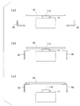
以下、本発明の一実施形態によるプリアライナー装置について図面を参照して説明する。 Hereinafter, a pre-aligner device according to an embodiment of the present invention will be described with reference to the drawings.
図1に示したように本実施形態によるプリアライナー装置10は、略円板状の半導体ウェハ30を保持して回転させるための回転機構11と、ウェハ30に予め形成されている位置決め用切り欠き部(ノッチ又はオリフラ)を検出するための検出機構12と、を備えている。
As shown in FIG. 1, the
回転機構11は、その載置面11A上に載置されたウェハ30を保持するためのチャック機構(図示を省略)を備えており、保持したウェハ30を回転軸線14周りに回転させる。
The
検出機構12は、回転機構11の載置面11A上に載置されたウェハ30の切欠き部を、例えば光学センサや撮像装置(CCDカメラ等)によって検出する。
The
本実施形態によるプリアライナー装置10は、さらに、位置合わせ後のウェハ30を回転機構11の載置面11Aから持ち上げるためのウェハ移送機構13を備えている。
The
このウェハ移送機構13は、回転機構11の回転軸線14を挟んで両側に配置された一対のピン部材(可動保持部)15と、一対のピン部材14同士の水平方向の離間距離を変更するための開閉駆動機構(水平駆動機構)と、一対のピン部材15を昇降させる昇降駆動機構とを備えている。
The
図2(a)に示したように一対のピン部材14は、互いの平行関係を維持しながら外側に水平移動して互いの離間距離を拡げることができる。
As shown in FIG. 2A, the pair of
図2(b)、(c)は開閉駆動機構の構成を示しており、一対のピン部材15はそれらの基端部が一対のリニアガイド40によって移動自在に支持されている。
FIGS. 2B and 2C show the configuration of the opening / closing drive mechanism, and the pair of
一対のピン部材15の各基端部には一対の第1リンク部材41のそれぞれの一端が枢着されており、各第1リンク部材41の他端は第2リンク部材42の各端部に枢着されている。
One end of each of the pair of
第2リンク部材42は、その中央部42aが回転可能に支持されている。第2リンク部材42の一端42bには、エアシリンダ43の出力軸43aの先端部が枢着されている。
The
エアシリンダ43は、プリアライナー装置10の制御部からの信号によって、出力軸43aの進退動作が制御される。
In the
図2(b)に示した状態からエアシリンダ43を駆動して出力軸43aを前進させると、第2リンク部材42がその中央部42aを支点として回転し、各第1リンク部材41が各ピン部材15を外側に向けて押す。これにより、各ピン部材15が各リニアガイド40上を外側に向けてスライドし、図2(c)に示したようにピン部材15同士の水平方向の間隔が拡がる。
When the
図3は開閉駆動機構の他の例を説明するための図であり、この例においては、図3(a)に示したように一対のピン部材15がそれらの基端部を中心として回転可能であり、これによりピン部材15同士の水平方向の間隔を拡げることができる。
FIG. 3 is a view for explaining another example of the opening / closing drive mechanism. In this example, as shown in FIG. 3A, the pair of
図3(b)、(c)はこの例における開閉駆動機構の構成を示しており、一対のピン部材15の各基端部が各回転軸線15aを中心として回転可能となっている。
FIGS. 3B and 3C show the configuration of the opening / closing drive mechanism in this example, and each base end portion of the pair of
各ピン部材15において、その回転軸線15aよりも基端側の部分には、一対の第1リンク部材51のそれぞれの一端が枢着されており、各第1リンク部材51の他端は第2リンク部材52の各端部に枢着されている。
In each
第2リンク部材52は、その中央部52aが回転可能に支持されている。第2リンク部材52の一端52bには、エアシリンダ53の出力軸53aの先端部が枢着されている。
As for the
エアシリンダ53は、プリアライナー装置10の制御部からの信号によって、出力軸53aの進退動作が制御される。
In the
図3(b)に示した状態からエアシリンダ53を駆動して出力軸53aを後退させると、第2リンク部材52がその中央部52aを支点として回転する。これにより、各第1リンク部材51が各ピン部材15を回転させ、図2(c)に示したようにピン部材15同士の水平方向の間隔が拡がる。
When the
図4は、ウェハ移送機構13の昇降駆動機構を示しており、エアシリンダ60の出力軸60aの先端部にベース部材61が設けられている。このベース部材61は、エアシリンダ60の出力軸60aを進退させることにより昇降する。
FIG. 4 shows a lift drive mechanism of the
エアシリンダ60は、プリアライナー装置10の制御部からの信号によって、出力軸60aの進退動作が制御される。
In the
図2又は図3に示した開閉駆動機構及び一対のピン部材15は、図4に示したベース部材61に配置されている。従って、エアシリンダ60を駆動することにより、一対のピン部材15を開閉駆動機構と共に昇降させることができる。
The opening / closing drive mechanism and the pair of
プリアライナー装置10の回転機構11上にウェハ30を載置する際には、ロボット20のアーム21を駆動して、アーム21の先端に設けられたハンド22によってカセット(図示を省略)からウェハ30を取り出し、さらにアーム21を駆動してウェハ30を回転機構11の載置面11A上に載置する。
When placing the
そして、回転機構11によってウェハ30を回転させながら、検出機構12によってウェハ30の切り欠き部を検出し、その検出結果に基づいてウェハ30の回転方向(θ方向)の位置合わせを行う。
And while rotating the
なお、検出機構12の検出結果に基づいて、ウェハ30が回転機構11の回転軸線14から偏心していると判断された場合には、算出された偏心量に基づいてハンド22によりウェハ30を回転機構11上の正しい位置に載置し直す。或いは、回転機構11をXY方向に移動可能に構成して、ウェハ30の偏心を回転機構11の移動によって調整するようにしても良い。
When it is determined that the
次に、図5及び図6を参照して、プリアライナー装置10から位置合わせ済みのウェハ30を取り出し、次のウェハ30を回転機構11上に載置する際の工程について説明する。
Next, with reference to FIG. 5 and FIG. 6, a process for taking out the aligned
ウェハ30を回転させて検出機構12でウェハ30の位置を検出する位置検出操作(アラインメント操作)中は、図5(a)に示したように一対のピン部材15は、互いに遠ざかった位置である退避位置に配置されている。
During the position detection operation (alignment operation) in which the
ウェハ30の位置検出操作が終了したら、ウェハ移送機構13の開閉駆動機構を作動させて、図5(b)に示したように一対のピン部材15同士を近づけてウェハ30の直下に移動させる。
When the position detection operation of the
この状態で、ウェハ移送機構13の昇降駆動機構を作動させて、図5(c)に示したように一対のピン部材15をウェハ30の裏面に当接させ、回転機構11の載置面11Aからウェハ30を垂直方向上方に持ち上げる。
In this state, the elevation drive mechanism of the
ウェハ30を持ち上げたときのピン部材15の高さ位置は、ロボット20のハンド22に載置した次のウェハ30を、ピン部材15と回転機構11との間に差し入れることができる位置である。
The height position of the
続いて、一対のピン部材15でウェハ30を持ち上げた状態で、図6(a)に示したように、ロボット20のハンド22によって次のウェハ30を回転機構11の載置面11A上に載置する。
Subsequently, in a state where the
このようにして次のウェハ30をハンド22により回転機構11上に載置したら、図6(b)に示したように、先ほどのハンド22を用いて一対のピン部材15上にある位置合わせ済みのウェハ30を搬出する。
When the
ピン部材15上からウェハ30が搬出されたら、図6(c)に示したように、ウェハ移送機構13の開閉駆動機構を作動させて一対のピン部材15同士の水平方向の離間距離を退避位置まで拡げる。
When the
このときのピン部材15同士の離間距離は、ピン部材15を降下させた際に回転機構11上に載置されているウェハ30にピン部材15が接触しない距離である。
The separation distance between the
次に、図6(d)に示したようにピン部材15を降下させ、次のウェハ30の位置合わせ操作を開始する。
Next, as shown in FIG. 6 (d), the
以上述べたように本実施形態によるプリアライナー装置10によれば、位置合わせ済みのウェハ30を次のウェハ30と交換する際に、位置合わせ済みのウェハ30をウェハ移送機構13によって持ち上げて暫定的に保持し、この状態で次のウェハ30をロボット20により搬入することができるので、プリアライナー装置10においてウェハ30の交換作業に要する時間を短縮することが可能であり、これによりウェハ処理のスループットをあげることができる。
As described above, according to the
上述した実施形態の一変形例として、図7及び図8に示したようにウェハ移送機構13の動作順序を変更することができる。
As a modification of the above-described embodiment, the operation order of the
即ち、ウェハ30の位置検出操作が終了したら、図7(a)に示したように、位置検出済みのウェハ30の上方に位置する一対のピン部材15上に、ロボット20のハンド22によって次のウェハ30を載置する。
That is, when the position detection operation of the
次に、図7(b)、(c)に示したように、ロボット20のハンド22によって位置検出済みのウェハ30を搬出する。
Next, as shown in FIGS. 7B and 7C, the position-detected
そして、ウェハ移送機構13の昇降駆動機構を作動させて、図7(d)に示したように一対のピン部材15を下降させ、回転機構11の載置面11A上に次のウェハ30を載置する。
Then, the elevation drive mechanism of the
その後、ウェハ移送機構13の開閉駆動機構を作動させて、図8(a)に示したように一対のピン部材15同士の水平方向の間隔を拡げて退避位置に配置する。
Thereafter, the opening / closing drive mechanism of the
この状態で、ウェハ移送機構13の昇降駆動機構を作動させて、一対のピン部材15を上昇させる。このときのピン部材15同士の離間距離は、ピン部材15を上昇させた際に回転機構11上に載置されているウェハ30にピン部材15が接触しない距離である。
In this state, the elevation drive mechanism of the
しかる後、ウェハ移送機構13の開閉駆動機構を作動させて、図8(c)に示したように一対のピン部材15同士を近づけてウェハ30の直上に移動させる。
Thereafter, the opening / closing drive mechanism of the
なお、ウェハ30の位置検出操作は、図8(c)に示した一対のピン部材15の閉鎖動作よりも前に実施される。
Note that the position detection operation of the
図7及び図8に示した例においても、プリアライナー装置10においてウェハ30の交換作業に要する時間を短縮することが可能であり、これによりウェハ処理のスループットをあげることができる。
Also in the example shown in FIGS. 7 and 8, it is possible to shorten the time required for the replacement work of the
なお、本発明によるプリアライナー装置におけるウェハ移送機構は、上述した実施形態におけるウェハ移送機構13に限定されるものではない。
The wafer transfer mechanism in the pre-aligner apparatus according to the present invention is not limited to the
即ち、本発明におけるウェハ移送機構は、回転機構11のウェハ載置面11Aの直上位置でウェハ30を保持するための可動保持部(上記実施形態ではピン部材15)を有し、回転機構11に保持されているウェハ30を回避して可動保持部が下降又は上昇するように構成されていれば良い。
That is, the wafer transfer mechanism in the present invention has a movable holding portion (in the above embodiment, the pin member 15) for holding the
例えば、上述した実施形態におけるウェハ移送機構13のピン部材15に代えて、図9に示したように断面L字型のL型部材16を設けると共に、このL型部材16をその長手方向に平行な軸線周りに回転可能に設けることができる。
For example, in place of the
この例においては、断面L字型のL型部材16の位置を、その回転動作によって、図9(a)に示した退避位置と図9(b)、(c)に示した作動位置とで適宜切り換えることができる。L型部材16の昇降駆動及び回転駆動は、例えばエアシリンダーによって行うことができる。
In this example, the position of the L-shaped
以上、本発明の好ましい実施形態について説明したが、上記実施形態は本発明の範囲内で適宜変更することができる。 As mentioned above, although preferable embodiment of this invention was described, the said embodiment can be suitably changed within the scope of the present invention.
Claims (4)
前記ウェハ移送機構は、前記ウェハ載置部の直上位置で前記ウェハを保持するための一対の細長部材を有し、前記一対の細長部材は、前記ウェハと平行な共通の平面において延びており、前記ウェハ移送機構は、前記回転機構に保持されているウェハを迂回して前記一対の細長部材が前記回転機構に保持されているウェハの上方位置から前記回転機構に保持されているウェハの下方位置に、またはその逆に、移動するように構成されていることを特徴とするプリアライナー装置。 A rotation mechanism for holding and rotating a semiconductor wafer, a detection mechanism for detecting a positioning notch formed on the wafer, and lifting the wafer from a wafer mounting portion of the rotation mechanism or the wafer A wafer transfer mechanism for mounting the wafer on the mounting portion,
The wafer transfer mechanism has a pair of elongated members for holding the wafer at a position immediately above the wafer mounting portion, and the pair of elongated members extend in a common plane parallel to the wafer, The wafer transfer mechanism bypasses the wafer held by the rotating mechanism and the lower position of the wafer held by the rotating mechanism from the upper position of the wafer where the pair of elongated members are held by the rotating mechanism. And / or vice versa, a pre-aligner device configured to move .
前記ウェハ移送機構は、前記ウェハを持ち上げる際に上昇して前記ウェハの裏面に当接される一対の細長部材を有し、前記一対の細長部材は、前記ウェハと平行な共通の平面において延びており、前記ウェハ移送機構は、前記一対の細長部材により持ち上げられた前記ウェハが搬出された後、前記回転機構に保持されている次のウェハを迂回して前記一対の細長部材が前記回転機構に保持されているウェハの上方位置から前記回転機構に保持されているウェハの下方位置に、またはその逆に、移動するように構成されていることを特徴とするプリアライナー装置。 A rotation mechanism for holding and rotating a semiconductor wafer, a detection mechanism for detecting a positioning notch formed on the wafer, and a wafer for lifting the wafer from a wafer mounting portion of the rotation mechanism A transfer mechanism,
The wafer transfer mechanism has a pair of elongated members that are raised when the wafer is lifted and are brought into contact with the back surface of the wafer, and the pair of elongated members extend in a common plane parallel to the wafer. cage, the wafer transfer mechanism, after the pair of elongate said wafer lifted by member is transported, said pair of elongate members to bypass the next wafer which is held by the rotating mechanism the rotating mechanism A pre-aligner device configured to move from an upper position of a held wafer to a lower position of the wafer held by the rotating mechanism or vice versa .
Applications Claiming Priority (1)
| Application Number | Priority Date | Filing Date | Title |
|---|---|---|---|
| PCT/JP2008/069138 WO2010046975A1 (en) | 2008-10-22 | 2008-10-22 | Prealigner |
Publications (2)
| Publication Number | Publication Date |
|---|---|
| JPWO2010046975A1 JPWO2010046975A1 (en) | 2012-03-15 |
| JP5295259B2 true JP5295259B2 (en) | 2013-09-18 |
Family
ID=42119036
Family Applications (1)
| Application Number | Title | Priority Date | Filing Date |
|---|---|---|---|
| JP2010534627A Active JP5295259B2 (en) | 2008-10-22 | 2008-10-22 | Pre-aligner device |
Country Status (5)
| Country | Link |
|---|---|
| US (1) | US9620401B2 (en) |
| EP (1) | EP2346073B1 (en) |
| JP (1) | JP5295259B2 (en) |
| KR (1) | KR101285988B1 (en) |
| WO (1) | WO2010046975A1 (en) |
Families Citing this family (6)
| Publication number | Priority date | Publication date | Assignee | Title |
|---|---|---|---|---|
| KR101489087B1 (en) * | 2013-08-27 | 2015-02-04 | 주식회사 에스에이치에너지화학 | Expandable polystyrene beads having thermal insulation property and method for fabricating thereof |
| WO2017027857A1 (en) * | 2015-08-12 | 2017-02-16 | Sarkis Sr Anthony Michael | Hot water heating system and related methods |
| CN112178010B (en) * | 2020-10-26 | 2023-03-14 | 中交第一航务工程局有限公司 | Control algorithm for regulation in submarine tunnel |
| CN114654394B (en) * | 2022-03-20 | 2022-11-01 | 上海图双精密装备有限公司 | Wafer detection moving carrier mechanism |
| KR102771986B1 (en) | 2024-05-31 | 2025-02-25 | 주식회사 리버스전자 | SiC wafer pre-aligner using infrared rays and SiC wafer pre-aligning method using infrared rays |
| KR102771994B1 (en) | 2024-05-31 | 2025-02-25 | 주식회사 리버스전자 | SiC wafer pre-aligner using infrared rays and SiC wafer pre-aligning method using infrared rays |
Citations (3)
| Publication number | Priority date | Publication date | Assignee | Title |
|---|---|---|---|---|
| JPH11165864A (en) * | 1997-12-03 | 1999-06-22 | Nikon Corp | Substrate conveying device and substrate treating device |
| JPH11288988A (en) * | 1998-04-04 | 1999-10-19 | Tokyo Electron Ltd | Alignment high-speed processing mechanism |
| JP2003347181A (en) * | 2002-05-24 | 2003-12-05 | Tokyo Electron Ltd | Substrate treatment device, substrate treatment method, and application/development device |
Family Cites Families (14)
| Publication number | Priority date | Publication date | Assignee | Title |
|---|---|---|---|---|
| US5100502A (en) * | 1990-03-19 | 1992-03-31 | Applied Materials, Inc. | Semiconductor wafer transfer in processing systems |
| JP3052105B2 (en) * | 1992-11-20 | 2000-06-12 | 東京エレクトロン株式会社 | Cleaning equipment |
| JPH0817894A (en) * | 1994-06-27 | 1996-01-19 | Dainippon Screen Mfg Co Ltd | Substrate surface treatment device |
| JPH11288995A (en) * | 1998-04-04 | 1999-10-19 | Tokyo Electron Ltd | Transfer system and processing device thereof |
| US6485248B1 (en) * | 2000-10-10 | 2002-11-26 | Applied Materials, Inc. | Multiple wafer lift apparatus and associated method |
| JP3956350B2 (en) * | 2002-03-25 | 2007-08-08 | 東京エレクトロン株式会社 | Substrate processing apparatus having positioning function and substrate processing method having positioning function |
| WO2004019387A1 (en) | 2002-08-22 | 2004-03-04 | Integrated Dynamics Engineering, Inc. | Substrate processing system |
| JP2004363218A (en) | 2003-06-03 | 2004-12-24 | Yaskawa Electric Corp | Pre-aligner equipment |
| US7019817B2 (en) * | 2003-07-14 | 2006-03-28 | Kawasaki Jukogyo Kabuishiki Kaisha | Edge-holding aligner |
| WO2006134760A1 (en) * | 2005-06-13 | 2006-12-21 | Kabushiki Kaisha Yaskawa Denki | Aligner |
| JP4884801B2 (en) * | 2005-10-06 | 2012-02-29 | 東京エレクトロン株式会社 | Processing system |
| JP4835839B2 (en) | 2006-04-07 | 2011-12-14 | 株式会社安川電機 | Transfer robot and position correction method for transfer robot |
| US8057153B2 (en) * | 2006-09-05 | 2011-11-15 | Tokyo Electron Limited | Substrate transfer device, substrate processing apparatus and substrate transfer method |
| US8950998B2 (en) * | 2007-02-27 | 2015-02-10 | Brooks Automation, Inc. | Batch substrate handling |
-
2008
- 2008-10-22 KR KR1020117009729A patent/KR101285988B1/en active IP Right Grant
- 2008-10-22 EP EP08877541.6A patent/EP2346073B1/en active Active
- 2008-10-22 JP JP2010534627A patent/JP5295259B2/en active Active
- 2008-10-22 US US13/124,777 patent/US9620401B2/en active Active
- 2008-10-22 WO PCT/JP2008/069138 patent/WO2010046975A1/en active Application Filing
Patent Citations (3)
| Publication number | Priority date | Publication date | Assignee | Title |
|---|---|---|---|---|
| JPH11165864A (en) * | 1997-12-03 | 1999-06-22 | Nikon Corp | Substrate conveying device and substrate treating device |
| JPH11288988A (en) * | 1998-04-04 | 1999-10-19 | Tokyo Electron Ltd | Alignment high-speed processing mechanism |
| JP2003347181A (en) * | 2002-05-24 | 2003-12-05 | Tokyo Electron Ltd | Substrate treatment device, substrate treatment method, and application/development device |
Also Published As
| Publication number | Publication date |
|---|---|
| EP2346073A4 (en) | 2012-05-02 |
| EP2346073A1 (en) | 2011-07-20 |
| US9620401B2 (en) | 2017-04-11 |
| KR20110065538A (en) | 2011-06-15 |
| US20110218663A1 (en) | 2011-09-08 |
| JPWO2010046975A1 (en) | 2012-03-15 |
| KR101285988B1 (en) | 2013-07-23 |
| EP2346073B1 (en) | 2017-05-24 |
| WO2010046975A1 (en) | 2010-04-29 |
Similar Documents
| Publication | Publication Date | Title |
|---|---|---|
| KR102379269B1 (en) | Robot with integrated aligner | |
| JP5295259B2 (en) | Pre-aligner device | |
| CN107534007B (en) | Substrate transfer robot and substrate processing system | |
| JP4858635B2 (en) | Aligner device | |
| TWI636858B (en) | Substrate transfer robot and substrate processing system | |
| KR100919215B1 (en) | End effector and robot arm apparatus having the same | |
| JP6263017B2 (en) | Substrate alignment apparatus and method for controlling substrate alignment apparatus | |
| JP5189370B2 (en) | Substrate exchange apparatus, substrate processing apparatus, and substrate inspection apparatus | |
| JP4835839B2 (en) | Transfer robot and position correction method for transfer robot | |
| KR20120105669A (en) | Edge grip type pre-aligner | |
| JP2010165706A (en) | Alignment device of wafer | |
| JP7429578B2 (en) | Aligner device and workpiece misalignment correction method | |
| JP4282379B2 (en) | Wafer inspection equipment | |
| JP7623023B2 (en) | Wafer Aligner | |
| JPH10116869A (en) | Wafer inspecting apparatus | |
| JP4446816B2 (en) | Substrate angular position correction device | |
| KR102386337B1 (en) | Die transfer module and die bonding apparatus having the same | |
| KR102386338B1 (en) | Die transfer module and die bonding apparatus having the same | |
| CN221687505U (en) | A clamping wafer pre-positioning device | |
| KR102350557B1 (en) | Die bonding method and die bonding apparatus | |
| KR100721567B1 (en) | Buffer arm device for semiconductor wafer aligner and alignment method using the same | |
| JP2023032305A (en) | Aligner device and positional deviation correction method for tabular work-piece | |
| KR20050076259A (en) | Apparatus for transfer a semiconductor substrate and equipment for manufacturing a semiconductor substrate having the same | |
| KR20210055910A (en) | Die transfer module and die bonding apparatus having the same | |
| JP2010186898A (en) | Bonding equipment |
Legal Events
| Date | Code | Title | Description |
|---|---|---|---|
| A131 | Notification of reasons for refusal |
Free format text: JAPANESE INTERMEDIATE CODE: A131 Effective date: 20121221 |
|
| A521 | Request for written amendment filed |
Free format text: JAPANESE INTERMEDIATE CODE: A523 Effective date: 20130204 |
|
| TRDD | Decision of grant or rejection written | ||
| A01 | Written decision to grant a patent or to grant a registration (utility model) |
Free format text: JAPANESE INTERMEDIATE CODE: A01 Effective date: 20130531 |
|
| A61 | First payment of annual fees (during grant procedure) |
Free format text: JAPANESE INTERMEDIATE CODE: A61 Effective date: 20130611 |
|
| R150 | Certificate of patent or registration of utility model |
Ref document number: 5295259 Country of ref document: JP Free format text: JAPANESE INTERMEDIATE CODE: R150 Free format text: JAPANESE INTERMEDIATE CODE: R150 |
|
| R250 | Receipt of annual fees |
Free format text: JAPANESE INTERMEDIATE CODE: R250 |
|
| R250 | Receipt of annual fees |
Free format text: JAPANESE INTERMEDIATE CODE: R250 |