JP5292682B2 - Power consumption reduction device, visibility improvement device, self-luminous display device, image processing device, electronic device, power consumption reduction method, visibility improvement method, and computer program - Google Patents
Power consumption reduction device, visibility improvement device, self-luminous display device, image processing device, electronic device, power consumption reduction method, visibility improvement method, and computer program Download PDFInfo
- Publication number
- JP5292682B2 JP5292682B2 JP2006247463A JP2006247463A JP5292682B2 JP 5292682 B2 JP5292682 B2 JP 5292682B2 JP 2006247463 A JP2006247463 A JP 2006247463A JP 2006247463 A JP2006247463 A JP 2006247463A JP 5292682 B2 JP5292682 B2 JP 5292682B2
- Authority
- JP
- Japan
- Prior art keywords
- gradation
- power consumption
- bits
- information
- conversion
- Prior art date
- Legal status (The legal status is an assumption and is not a legal conclusion. Google has not performed a legal analysis and makes no representation as to the accuracy of the status listed.)
- Expired - Fee Related
Links
- 230000009467 reduction Effects 0.000 title claims description 55
- 238000000034 method Methods 0.000 title description 40
- 230000006872 improvement Effects 0.000 title description 5
- 238000004590 computer program Methods 0.000 title description 2
- 238000006243 chemical reaction Methods 0.000 claims description 133
- 238000004364 calculation method Methods 0.000 claims description 24
- 230000002093 peripheral effect Effects 0.000 description 24
- 230000008569 process Effects 0.000 description 18
- 238000004891 communication Methods 0.000 description 9
- 238000003384 imaging method Methods 0.000 description 9
- 239000003990 capacitor Substances 0.000 description 6
- 230000010365 information processing Effects 0.000 description 6
- 230000008859 change Effects 0.000 description 5
- 239000000470 constituent Substances 0.000 description 5
- 230000003247 decreasing effect Effects 0.000 description 4
- 230000007246 mechanism Effects 0.000 description 4
- 238000001514 detection method Methods 0.000 description 2
- 238000005516 engineering process Methods 0.000 description 2
- 238000012986 modification Methods 0.000 description 2
- 230000004048 modification Effects 0.000 description 2
- 230000015556 catabolic process Effects 0.000 description 1
- 230000001413 cellular effect Effects 0.000 description 1
- 239000003086 colorant Substances 0.000 description 1
- 230000006837 decompression Effects 0.000 description 1
- 238000006731 degradation reaction Methods 0.000 description 1
- 230000000694 effects Effects 0.000 description 1
- 238000005286 illumination Methods 0.000 description 1
- 238000004519 manufacturing process Methods 0.000 description 1
- 239000011159 matrix material Substances 0.000 description 1
- 239000003973 paint Substances 0.000 description 1
- 239000004065 semiconductor Substances 0.000 description 1
Images


Classifications
-
- G—PHYSICS
- G09—EDUCATION; CRYPTOGRAPHY; DISPLAY; ADVERTISING; SEALS
- G09G—ARRANGEMENTS OR CIRCUITS FOR CONTROL OF INDICATING DEVICES USING STATIC MEANS TO PRESENT VARIABLE INFORMATION
- G09G3/00—Control arrangements or circuits, of interest only in connection with visual indicators other than cathode-ray tubes
- G09G3/20—Control arrangements or circuits, of interest only in connection with visual indicators other than cathode-ray tubes for presentation of an assembly of a number of characters, e.g. a page, by composing the assembly by combination of individual elements arranged in a matrix no fixed position being assigned to or needed to be assigned to the individual characters or partial characters
- G09G3/2007—Display of intermediate tones
-
- G—PHYSICS
- G06—COMPUTING; CALCULATING OR COUNTING
- G06F—ELECTRIC DIGITAL DATA PROCESSING
- G06F1/00—Details not covered by groups G06F3/00 - G06F13/00 and G06F21/00
- G06F1/26—Power supply means, e.g. regulation thereof
- G06F1/32—Means for saving power
-
- G—PHYSICS
- G09—EDUCATION; CRYPTOGRAPHY; DISPLAY; ADVERTISING; SEALS
- G09G—ARRANGEMENTS OR CIRCUITS FOR CONTROL OF INDICATING DEVICES USING STATIC MEANS TO PRESENT VARIABLE INFORMATION
- G09G3/00—Control arrangements or circuits, of interest only in connection with visual indicators other than cathode-ray tubes
- G09G3/20—Control arrangements or circuits, of interest only in connection with visual indicators other than cathode-ray tubes for presentation of an assembly of a number of characters, e.g. a page, by composing the assembly by combination of individual elements arranged in a matrix no fixed position being assigned to or needed to be assigned to the individual characters or partial characters
- G09G3/22—Control arrangements or circuits, of interest only in connection with visual indicators other than cathode-ray tubes for presentation of an assembly of a number of characters, e.g. a page, by composing the assembly by combination of individual elements arranged in a matrix no fixed position being assigned to or needed to be assigned to the individual characters or partial characters using controlled light sources
- G09G3/30—Control arrangements or circuits, of interest only in connection with visual indicators other than cathode-ray tubes for presentation of an assembly of a number of characters, e.g. a page, by composing the assembly by combination of individual elements arranged in a matrix no fixed position being assigned to or needed to be assigned to the individual characters or partial characters using controlled light sources using electroluminescent panels
- G09G3/32—Control arrangements or circuits, of interest only in connection with visual indicators other than cathode-ray tubes for presentation of an assembly of a number of characters, e.g. a page, by composing the assembly by combination of individual elements arranged in a matrix no fixed position being assigned to or needed to be assigned to the individual characters or partial characters using controlled light sources using electroluminescent panels semiconductive, e.g. using light-emitting diodes [LED]
- G09G3/3208—Control arrangements or circuits, of interest only in connection with visual indicators other than cathode-ray tubes for presentation of an assembly of a number of characters, e.g. a page, by composing the assembly by combination of individual elements arranged in a matrix no fixed position being assigned to or needed to be assigned to the individual characters or partial characters using controlled light sources using electroluminescent panels semiconductive, e.g. using light-emitting diodes [LED] organic, e.g. using organic light-emitting diodes [OLED]
-
- G—PHYSICS
- G09—EDUCATION; CRYPTOGRAPHY; DISPLAY; ADVERTISING; SEALS
- G09G—ARRANGEMENTS OR CIRCUITS FOR CONTROL OF INDICATING DEVICES USING STATIC MEANS TO PRESENT VARIABLE INFORMATION
- G09G5/00—Control arrangements or circuits for visual indicators common to cathode-ray tube indicators and other visual indicators
- G09G5/10—Intensity circuits
-
- H—ELECTRICITY
- H04—ELECTRIC COMMUNICATION TECHNIQUE
- H04N—PICTORIAL COMMUNICATION, e.g. TELEVISION
- H04N9/00—Details of colour television systems
- H04N9/64—Circuits for processing colour signals
-
- G—PHYSICS
- G09—EDUCATION; CRYPTOGRAPHY; DISPLAY; ADVERTISING; SEALS
- G09G—ARRANGEMENTS OR CIRCUITS FOR CONTROL OF INDICATING DEVICES USING STATIC MEANS TO PRESENT VARIABLE INFORMATION
- G09G2320/00—Control of display operating conditions
- G09G2320/02—Improving the quality of display appearance
- G09G2320/0271—Adjustment of the gradation levels within the range of the gradation scale, e.g. by redistribution or clipping
-
- G—PHYSICS
- G09—EDUCATION; CRYPTOGRAPHY; DISPLAY; ADVERTISING; SEALS
- G09G—ARRANGEMENTS OR CIRCUITS FOR CONTROL OF INDICATING DEVICES USING STATIC MEANS TO PRESENT VARIABLE INFORMATION
- G09G2330/00—Aspects of power supply; Aspects of display protection and defect management
- G09G2330/02—Details of power systems and of start or stop of display operation
- G09G2330/021—Power management, e.g. power saving
-
- G—PHYSICS
- G09—EDUCATION; CRYPTOGRAPHY; DISPLAY; ADVERTISING; SEALS
- G09G—ARRANGEMENTS OR CIRCUITS FOR CONTROL OF INDICATING DEVICES USING STATIC MEANS TO PRESENT VARIABLE INFORMATION
- G09G2360/00—Aspects of the architecture of display systems
- G09G2360/14—Detecting light within display terminals, e.g. using a single or a plurality of photosensors
- G09G2360/144—Detecting light within display terminals, e.g. using a single or a plurality of photosensors the light being ambient light
-
- G—PHYSICS
- G09—EDUCATION; CRYPTOGRAPHY; DISPLAY; ADVERTISING; SEALS
- G09G—ARRANGEMENTS OR CIRCUITS FOR CONTROL OF INDICATING DEVICES USING STATIC MEANS TO PRESENT VARIABLE INFORMATION
- G09G3/00—Control arrangements or circuits, of interest only in connection with visual indicators other than cathode-ray tubes
- G09G3/20—Control arrangements or circuits, of interest only in connection with visual indicators other than cathode-ray tubes for presentation of an assembly of a number of characters, e.g. a page, by composing the assembly by combination of individual elements arranged in a matrix no fixed position being assigned to or needed to be assigned to the individual characters or partial characters
- G09G3/2007—Display of intermediate tones
- G09G3/2014—Display of intermediate tones by modulation of the duration of a single pulse during which the logic level remains constant
Landscapes
- Engineering & Computer Science (AREA)
- Theoretical Computer Science (AREA)
- Physics & Mathematics (AREA)
- General Physics & Mathematics (AREA)
- Computer Hardware Design (AREA)
- Multimedia (AREA)
- Signal Processing (AREA)
- General Engineering & Computer Science (AREA)
- Control Of Indicators Other Than Cathode Ray Tubes (AREA)
- Control Of El Displays (AREA)
- Electroluminescent Light Sources (AREA)
Description
この明細書で説明する発明は、周辺照度が高い状況での視認性の低下を最小限にとどめながら消費電力を削減する技術及び消費電力の増加を最小限にとどめながら視認性を向上する技術に関する。 The invention described in this specification relates to a technique for reducing power consumption while minimizing a decrease in visibility in a situation where ambient illuminance is high, and a technique for improving visibility while minimizing an increase in power consumption. .
発明者らが提案する発明は、消費電力削減装置、視認性向上装置、自発光表示装置、画像処理装置、電子機器、消費電力削減方法、視認性向上方法及びコンピュータプログラムとしての側面を有する。 The invention proposed by the inventors has aspects as a power consumption reducing device, a visibility improving device, a self-luminous display device, an image processing device, an electronic device, a power consumption reducing method, a visibility improving method, and a computer program.
今日、フラットパネルディスプレイは、様々な電子機器に搭載されている。これに伴い、フラットパネルディスプレイの使用環境も多様化してきている。例えば非常に照度の高い環境下でフラットパネルディスプレイを使用する機会も増えている。 Today, flat panel displays are mounted on various electronic devices. As a result, the usage environment of flat panel displays has also diversified. For example, there are increasing opportunities to use flat panel displays in very high illumination environments.
ところで、使用環境の照度が高いと、画面の視認性が極端に低下する。このような場合に視認性を高めるには、画面輝度を上げる必要がある。 By the way, when the illuminance of the use environment is high, the visibility of the screen is extremely lowered. In such a case, in order to increase the visibility, it is necessary to increase the screen brightness.
しかし、画面輝度を上げると、一般に消費電力が高くなる。特に自発光型のフラットパネルディスプレイの場合、画面輝度の上昇は消費電力の増加に直結する問題がある。更に携帯型の電子機器の場合、消費電力の増加は使用時間の短縮に直結する。 However, increasing screen brightness generally increases power consumption. In particular, in the case of a self-luminous flat panel display, there is a problem that an increase in screen brightness directly leads to an increase in power consumption. Furthermore, in the case of portable electronic devices, an increase in power consumption directly leads to a reduction in usage time.
そこで発明者らは、低階調域に対応するn1ビット分の階調情報をm1(<n1)ビット分の階調情報に変換し、中間階調域に対応するn2ビット分の階調情報をm2(≦n2)ビット分の階調情報に変換し、高階調域に対応するn3ビット分の階調情報をm3(<n3)ビット分の階調情報に変換する階調域適応型の階調変換部であって、m1≦m2かつm3≦m2、かつ、n1+n2+n3>m1+m2+m3を満たすように入力映像信号を階調変換する階調変換部を有する消費電力削減装置を提案する。 Therefore, the inventors convert gradation information for n1 bits corresponding to the low gradation region into gradation information for m1 (<n1) bits, and gradation information for n2 bits corresponding to the intermediate gradation region. Is converted to gradation information for m2 (≦ n2) bits, and gradation information for n3 bits corresponding to the high gradation area is converted to gradation information for m3 (<n3) bits. A power consumption reduction device is proposed that includes a gradation conversion unit that converts a gradation of an input video signal so that m1 ≦ m2 and m3 ≦ m2 and n1 + n2 + n3> m1 + m2 + m3.
周辺環境の照度が高い場合、一般に中間階調域に比べ、低階調域や高階調域の視認性が低下する。発明者らの提案する技術手法では、これら階調域の階調情報を積極的に削減する。これにより、実際の視認性には影響を与えずに、消費電力を削減することができる。 When the illuminance in the surrounding environment is high, the visibility in the low gradation area and the high gradation area is generally lower than in the intermediate gradation area. In the technical technique proposed by the inventors, the gradation information in these gradation regions is actively reduced. Thereby, power consumption can be reduced without affecting the actual visibility.
なお、この階調変換による消費電力の削減量の範囲でピーク輝度レベルを上げれば、従来技術に比して視認性を向上することができる。すなわち、消費電力の増加を伴わずに画面の視認性を高めることができる。 Note that if the peak luminance level is increased within the range of reduction in power consumption due to this gradation conversion, the visibility can be improved as compared with the prior art. That is, the visibility of the screen can be enhanced without increasing power consumption.
以下、発明に係る消費電力の削減技術及び視認性の向上技術を説明する。
なお、本明細書で特に図示又は記載されない部分には、当該技術分野の周知又は公知技術を適用する。
また以下に説明する形態例は、発明の一つの形態例であって、これらに限定されるものではない。
Hereinafter, the power consumption reduction technology and the visibility improvement technology according to the invention will be described.
In addition, the well-known or well-known technique of the said technical field is applied to the part which is not illustrated or described in particular in this specification.
Moreover, the form example demonstrated below is one form example of invention, Comprising: It is not limited to these.
(A)形態例1
(A−1)消費電力削減装置の機能構成
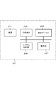
図1に、消費電力削減装置1の機能構成例を示す。
消費電力削減装置1は、平均階調値算出部3及び階調域別階調変換部5で構成される。
(A) Form example 1
(A-1) Functional Configuration of Power Consumption Reduction Device FIG. 1 shows a functional configuration example of the power
The power
平均階調値算出部3は、1フレーム当たりの平均階調値(APL:average picture level )を映像信号に基づいて算出する処理デバイスである。なお、平均階調値の算出は、1フレーム単位で実行しても良いし、複数フレーム期間に入力された映像信号のフレーム平均値として算出しても良い。
The average gradation
階調域別階調変換部5は、周辺輝度が高い場合、平均階調値を中心に設定した一定範囲の階調情報を多く残す一方で、低階調域と高階調域の階調情報は積極的に削減する階調変換処理を実行する処理デバイスである。なお、周辺輝度が高く無い場合(周辺輝度が判定閾値より小さい場合)、階調域別階調変換部5は、入力時のまま映像信号を出力する。
When the peripheral luminance is high, the
図2に、階調域別階調変換部5の内部構成例を示す。階調域別階調変換部5は、階調域設定部11と演算部13とで構成される。
階調域設定部11は、周辺輝度が高い場合、平均階調値に基づいて低階調域、中間階調域、高階調域を設定し、周辺輝度が高く無い場合、階調域の設定を停止する。
FIG. 2 shows an internal configuration example of the
The gradation
この形態例の場合、階調域設定部11は、平均階調値−全階調域/2と平均階調域+全階調域/2を算出し、これら2つの階調値に基づいて3つの階調域を設定する。
すなわち、平均階調値−全階調域/2と平均階調域+全階調域/2で挟まれる階調域を中間階調域、平均階調値−全階調域/2より小さい階調域を低階調域、平均階調値+全階調域/2より大きい階調域を高階調域に設定する。
In the case of this embodiment, the gradation
That is, the gradation range sandwiched between the average gradation value−all gradation regions / 2 and the average gradation region + all gradation regions / 2 is smaller than the intermediate gradation region, and the average gradation value−all gradation regions / 2. The gradation area is set to the low gradation area, and the gradation area larger than the average gradation value + the entire gradation area / 2 is set to the high gradation area.
図3に、平均階調値に応じた階調域の設定例を示す。図3は、映像信号が8ビットの場合(映像信号が256階調の場合)における設定例である。従って、中間階調域の階調幅は128階調幅に設定される。また、低階調域と中間階調域の境界点を与える階調値は、平均階調値−64で与えられる。他方、高階調域と中間階調域の境界点を与える階調値は、平均階調値+64で与えられる。 FIG. 3 shows a setting example of the gradation range according to the average gradation value. FIG. 3 shows a setting example when the video signal is 8 bits (when the video signal has 256 gradations). Therefore, the gradation width of the intermediate gradation area is set to 128 gradation width. The gradation value that provides the boundary point between the low gradation area and the intermediate gradation area is given by an average gradation value of −64. On the other hand, the gradation value that provides the boundary point between the high gradation area and the intermediate gradation area is given by the average gradation value +64.
例えば平均階調値が“128”の場合、低階調域は“1”〜“64”に、中間階調域は“65”〜“191”に、高階調域は“192”〜“256”に設定される。 For example, when the average gradation value is “128”, the low gradation range is “1” to “64”, the intermediate gradation range is “65” to “191”, and the high gradation range is “192” to “256”. "Is set.
図4に、平均階調値の違いに応じて各階調域の設定範囲が変化する様子を示す。なお、中間階調域の幅は、平均階調値の違いによらず常に同じであるものとする。図4(A)は、平均階調値が小さい場合の例である。低階調域が狭くなる一方で、高階調域が広くなっている。 FIG. 4 shows how the setting range of each gradation area changes in accordance with the difference in average gradation value. The width of the intermediate gradation area is always the same regardless of the difference in the average gradation value. FIG. 4A shows an example where the average gradation value is small. While the low gradation region is narrowed, the high gradation region is widened.
図4(B)は、平均階調値が中間値の例である。低階調域と高階調域がほぼ同じ階調幅で与えられる。図4(C)は、平均階調値が大きい場合の例である。低階調域が広い一方で、高階調域が狭くなっている。 FIG. 4B shows an example in which the average gradation value is an intermediate value. The low gradation region and the high gradation region are given with substantially the same gradation width. FIG. 4C shows an example where the average gradation value is large. While the low gradation range is wide, the high gradation range is narrow.
演算部13は、各画素に対応する映像信号(階調値)が属する階調域別に応じた階調変換処理を演算処理により実行する処理デバイスである。
この形態例の場合、各階調域に割り当てる階調情報(ビット数)は、事前に設定されているものとする。
The
In the case of this embodiment, it is assumed that gradation information (number of bits) assigned to each gradation area is set in advance.
図3の場合、低階調域には、4ビット(16階調)分の階調情報が割り当てられている。中間階調域には、6ビット(64階調)分の階調情報が割り当てられている。高階調域には、4ビット(16階調)分の階調情報が割り当てられている。 In the case of FIG. 3, gradation information for 4 bits (16 gradations) is assigned to the low gradation area. Tone gradation information is assigned gradation information for 6 bits (64 gradations). Gradation information for 4 bits (16 gradations) is assigned to the high gradation area.
従って、この演算部13による階調変換が実施されると256階調の階調情報を有する映像信号は、96階調(=16階調+64階調+16階調)の階調情報を有する映像信号に変換される。
図5に、映像信号の属する階調域別に適用される演算式を示す。勿論、図5は、映像信号が8ビットで与えられる場合において、中間階調域が全階調域の半分として与えられる場合について表している。
Therefore, when the gradation conversion by the
FIG. 5 shows an arithmetic expression applied to each gradation region to which the video signal belongs. Of course, FIG. 5 shows a case where the intermediate gradation area is given as half of the whole gradation area when the video signal is given by 8 bits.
階調変換では、入力階調値を各階調域内で正規化した値を単位ステップ値で除算する処理(同階調域におけるステップ数を算出する処理)と、算出されたステップ数に単位ステップ値を乗算する処理(出力階調値を求める処理)とが実行される。なお、中間階調域や高階調域については、各階調域の原点に対応する階調値(オフセット量)を、先の演算結果に加算する処理が合わせて実行される。 In gradation conversion, the process of dividing the input gradation value normalized within each gradation range by the unit step value (processing for calculating the number of steps in the same gradation range), and the unit step value to the calculated number of steps And a process for obtaining the output gradation value are performed. For the intermediate gradation area and the high gradation area, a process of adding a gradation value (offset amount) corresponding to the origin of each gradation area to the previous calculation result is also executed.
なお、図5に示す演算式において、演算子NINTは、四捨五入による整数値化処理を意味する。
例えば平均階調値が“128”の場合、低階調域に属する映像信号(階調値)は、4階調単位で階調値が階段上に変化する映像信号に変換される。
In the arithmetic expression shown in FIG. 5, the operator NINT means an integer value conversion process by rounding off.
For example, when the average gradation value is “128”, the video signal (gradation value) belonging to the low gradation range is converted into a video signal in which the gradation value changes on a staircase in units of 4 gradations.
同様に、平均階調値が“128”の場合、中間階調域に属する映像信号(階調値)は、2階調単位で階調値が階段上に変化する映像信号に変換される。
同様に、平均階調値が“128”の場合、高階調域に属する映像信号(階調値)は、4階調単位で階調値が階段上に変化する映像信号に変換される。
Similarly, when the average gradation value is “128”, the video signal (gradation value) belonging to the intermediate gradation range is converted into a video signal whose gradation value changes stepwise in units of two gradations.
Similarly, when the average gradation value is “128”, the video signal (gradation value) belonging to the high gradation range is converted into a video signal in which the gradation value changes stepwise in units of 4 gradations.
図3では、この入出力関係を、階段状の太線として表している。なお、階調変換を実行しない場合の入出力関係は、図3に細線で示すように直線状となる。
このように、周辺輝度に応じて選択的に実行される階調変換の結果が、表示デバイス7に出力される。
In FIG. 3, this input / output relationship is represented as a thick staircase. The input / output relationship when gradation conversion is not executed is linear as shown by a thin line in FIG.
As described above, the result of the gradation conversion that is selectively executed according to the peripheral luminance is output to the
(A−2)表示デバイスの構成
この形態例の場合、表示デバイスは自発光表示デバイスの一つである有機ELディスプレイを想定する。
図6に、表示デバイス7の機能構成例を示す。表示デバイス7は、タイミングジェネレータ21、データ線ドライバ23、スキャンドライバ25、スキャンドライバ27、電源電圧源29及び有機ELディスプレイパネル31で構成される。
(A-2) Configuration of Display Device In the case of this embodiment, the display device is assumed to be an organic EL display that is one of self-luminous display devices.
FIG. 6 shows a functional configuration example of the
タイミングジェネレータ21は、消費電力削減装置1より与えられる映像信号に含まれるタイミング信号に基づいて画面表示に必要な各種のタイミング信号を発生する処理デバイスである。例えば書き込みパルス等を発生する。
The
データ線ドライバ23は、有機ELディスプレイパネル31のデータ線を駆動する回路デバイスである。
データ線ドライバ23は、各画素の発光輝度を指定する階調値をアナログ電圧値に変換し、データ線に供給する動作を実行する。
The
The
スキャンドライバ25は、階調値を書き込む水平ラインの選択用に設けられたゲート線を線順次に選択する回路デバイスである。この選択信号が書き込みパルスとして、有機ELディスプレイパネル31に供給される。この形態例におけるスキャンドライバ25は、水平ライン別に書き込みパルスを出力する。
The
スキャンドライバ27は、デューティパルス信号の供給用に設けられたゲート線を駆動する回路デバイスである。ここでのデューティパルス信号は、1フレーム期間内における点灯時間長を与える信号をいう。図7に、デューティパルス信号の一例を示す。図7(A)は最大点灯時間長の最大期間を与える垂直同期パルスである。図7(B)はデューティパルス信号例である。図7(B)の場合、Lレベルの期間が1フレーム期間内の点灯時間長になる。この形態例の場合、点灯時間は固定であるものとする。
The
電源電圧源29は、有機EL素子の陽極側に印可する電源電圧(アナログ電圧)を供給する回路デバイスである。この形態例の場合、電源電圧源29は一定電圧を発生する。
有機ELディスプレイパネル31は、有機EL素子がマトリクス状に配置された表示デバイスである。なお、有機ELディスプレイパネル31はカラー表示用である。従って、表示上の1画素(ピクセル)は、RGBの三色に対応する画素(サブピクセル)で構成される。
The power
The organic
図8に、データ線とゲート線との交点位置に形成される画素回路41と周辺回路との接続関係を示す。
画素回路41は、データスイッチ素子T1、キャパシタC1、電流供給素子T2、点灯期間制御素子T3で構成される。
FIG. 8 shows a connection relationship between the
The
ここで、データスイッチ素子T1は、データ線を通じて与えられる電圧値の取り込み(書き込み)を制御するトランジスタである。電圧値の取り込みタイミングは、水平ライン単位で与えられる。 Here, the data switch element T1 is a transistor that controls the capturing (writing) of the voltage value applied through the data line. The voltage value capture timing is given in units of horizontal lines.
キャパシタC1は、取り込んだ電圧値を1フレームの間保持する記憶素子である。キャパシタC1を用いることで、データの書き込みが線順次走査の場合でも、面順次走査と同様の発光態様が実現される。 The capacitor C1 is a storage element that holds the acquired voltage value for one frame. By using the capacitor C1, even in the case where the data is written by line sequential scanning, a light emission mode similar to that of the surface sequential scanning is realized.
電流供給素子T2は、キャパシタC1の電圧値に応じた駆動電流を有機EL素子D1に供給するトランジスタである。
点灯期間制御素子T3は、有機EL素子D1の点灯時間を1フレーム内で制御するトランジスタである。
The current supply element T2 is a transistor that supplies a drive current corresponding to the voltage value of the capacitor C1 to the organic EL element D1.
The lighting period control element T3 is a transistor that controls the lighting time of the organic EL element D1 within one frame.
点灯期間制御素子T3は、駆動電流の供給経路に対して直列に配置される。点灯期間制御素子T3がオン動作している間、有機EL素子D1が点灯する。一方、点灯期間制御素子T3がオフ動作している間、有機EL素子D1が消灯する。
この点灯期間制御素子T3に印加される信号が、前述したデューティパルス信号(図7)である。
The lighting period control element T3 is arranged in series with respect to the drive current supply path. While the lighting period control element T3 is on, the organic EL element D1 is lit. On the other hand, the organic EL element D1 is turned off while the lighting period control element T3 is turned off.
The signal applied to the lighting period control element T3 is the aforementioned duty pulse signal (FIG. 7).
(A−3)階調変換処理
以下、周辺輝度が高い場合に実行される階調変換動作を説明する。なお、階調変換動作は、外光センサーから入力される周辺輝度情報が判定閾値より大きい場合に実行される。
図9に、階調域が設定されるまでの処理手順を示す。なお、図9に示す処理動作は、1フレーム周期で実行される。
(A-3) Gradation Conversion Processing Hereinafter, the gradation conversion operation executed when the peripheral luminance is high will be described. Note that the gradation conversion operation is executed when the peripheral luminance information input from the external light sensor is larger than the determination threshold.
FIG. 9 shows a processing procedure until the gradation area is set. Note that the processing operation shown in FIG. 9 is executed in a cycle of one frame.
まず、消費電力削減装置1は、1フレーム当たりの平均階調値を算出する(S1)。
次に、消費電力削減装置1は、平均階調値に応じて低階調域、中間階調域、高階調域をそれぞれ設定する(S2)。
First, the power
Next, the power
具体的に低階調域が設定されると、消費電力削減装置1は、各階調域の変換演算で使用するパラメータを設定する(S3)。具体的には、図5で説明した演算式における入力階調以外のパラメータを設定する。
Specifically, when the low gradation range is set, the power
このパラメータの設定後、消費電力削減装置1は、画素毎に図10に示す処理動作を実行する。
まず、消費電力削減装置1は、入力階調が低階調域か否かを判定する(S11)。
肯定結果が得られた場合、消費電力削減装置1は、低階調域用の階調変換処理を実行する(S12)。
After the setting of this parameter, the power
First, the power
When an affirmative result is obtained, the power
これに対し、否定結果が得られた場合、消費電力削減装置1は、入力階調が中間階調域か否かを判定する(S13)。
肯定結果が得られた場合、消費電力削減装置1は、中間階調域用の階調変換処理を実行する(S14)。
On the other hand, when a negative result is obtained, the power
When an affirmative result is obtained, the power
一方、否定結果が得られた場合、消費電力削減装置1は、高階調域用の階調変換処理を実行する(S15)。
この図10に示す一連の動作が、1フレームを構成する全画素について繰り返し実行される。結果的に、256階調を有する映像信号が96階調の映像信号に変換され、表示画面上に表示される。
On the other hand, when a negative result is obtained, the power
A series of operations shown in FIG. 10 are repeatedly executed for all the pixels constituting one frame. As a result, a video signal having 256 gradations is converted to a 96 gradation video signal and displayed on the display screen.
(A−4)階調変換の効果
以上説明したように、階調情報を削減しながらも、中間階調域に多くの階調情報を割り当てることにより、周辺輝度が高い場合でも、視認性を落とすことなく消費電力を削減することができる。
(A-4) Effect of Tone Conversion As described above, by assigning a large amount of tone information to the intermediate tone range while reducing the tone information, visibility is improved even when the peripheral luminance is high. Power consumption can be reduced without dropping.
図11に、消費電力が削減される様子を視覚的に示す。図11は、消費電力が削減される部分と量を黒色の塗りつぶしパターンで示している。階調情報の削減量が大きい低階調域と高階調域ほど消費電力の削減量が大きくなっている。 FIG. 11 visually shows how power consumption is reduced. FIG. 11 shows a portion and amount of power consumption reduced by a black paint pattern. The amount of reduction in power consumption increases as the gradation level and the gradation level where the gradation information reduction amount is large.
なお前述したように、周辺輝度が高い環境では確認できるコントラスト差はもともと小さい。これに加え、平均階調値を基準に設定した中間階調域の階調情報を多く残すことで視認性の低下を最小限にとどめることができる。すなわち、視認性には影響を与えることなく、消費電力を確実に低下できる。 As described above, the contrast difference that can be confirmed is originally small in an environment where the peripheral luminance is high. In addition to this, by leaving a large amount of gradation information in the intermediate gradation range set based on the average gradation value, it is possible to minimize degradation in visibility. That is, power consumption can be reliably reduced without affecting visibility.
特に有機EL表示ディスプレイを屋外で使用する場合には、この消費電力の削減を使用可能時間の延長に使うことができる。 In particular, when the organic EL display is used outdoors, this reduction in power consumption can be used to extend the usable time.
(B)形態例2
ここでは、階調変換テーブルを用いて階調域別の階調変換機能を実現する場合について説明する。なお、基本的なシステム構成は、形態例1で説明した図1の構成と同じである。ただし、階調域別階調変換部の内部構成が異なる。
(B)
Here, a case where a gradation conversion function for each gradation area is realized using a gradation conversion table will be described. The basic system configuration is the same as the configuration of FIG. However, the internal configuration of the gradation conversion unit for each gradation region is different.
図12に、階調域別階調変換部51の内部構成例を示す。
階調域別階調変換部51は、テーブル選択部53及び変換テーブル55で構成される。
テーブル選択部53は、周辺輝度が高い場合、平均階調値に基づいて最適な変換テーブルを選択し、周辺輝度が高く無い場合、変換処理を停止する(または、入力階調値と出力階調値が同じ変換テーブルを選択する)。
FIG. 12 shows an internal configuration example of the
The
The
変換テーブル55は、算出される平均階調値を予測して事前に用意された複数組の変換テーブルで構成される。厳密には、256階調分だけ変換テーブルを用意することになるが、実用上は使用頻度や階調変換の変化量を考慮して代表的な複数組だけ搭載する。従って、テーブル選択部53は、算出された平均階調値を想定範囲に含む変換テーブルを選択する動作を実行する。
The conversion table 55 includes a plurality of conversion tables prepared in advance by predicting the calculated average gradation value. Strictly speaking, a conversion table is prepared for 256 gradations, but in practice, only a plurality of representative sets are mounted in consideration of the usage frequency and the amount of change in gradation conversion. Therefore, the
図13に、変換テーブル55のテーブル構造を示す。図13に示すように、変換テーブル55は、入力階調値と出力階調値の対応関係を保存する。勿論、対応関係は、形態例1で説明した階調域別の階調変換式を満たしている。 FIG. 13 shows the table structure of the conversion table 55. As shown in FIG. 13, the conversion table 55 stores the correspondence between the input gradation value and the output gradation value. Of course, the correspondence relationship satisfies the gradation conversion formula for each gradation region described in the first embodiment.
なお、図13では、256階調全ての階調値と出力階調値との対応関係を記録しているが、出力階調値が変化する部分の対応関係のみを記憶し、対応関係のない階調値については入力階調値よりも小さい側で最も近い階調に対応付けられた出力階調値を読み出す仕組みを採用しても良い。このような仕組みを採用すれば、変換テーブル55に要求される記憶容量を削減することができる。 In FIG. 13, the correspondence relationship between the gradation values of all 256 gradations and the output gradation value is recorded, but only the correspondence relationship of the portion where the output gradation value changes is stored, and there is no correspondence relationship. For the gradation value, a mechanism of reading the output gradation value associated with the closest gradation on the side smaller than the input gradation value may be adopted. By adopting such a mechanism, the storage capacity required for the conversion table 55 can be reduced.
図14に、変換テーブルが設定されるまでの処理手順を示す。なお、図14に示す処理動作は、1フレーム周期で実行される。
この場合も、平均階調値算出部3によって、1フレーム当たりの平均階調値が算出される(S21)。
次に、階調域別階調変換部51が、平均階調値に応じて低階調域、中間階調域、高階調域が設定された変換テーブルを設定する(S22)。
FIG. 14 shows a processing procedure until the conversion table is set. Note that the processing operation shown in FIG. 14 is executed in a cycle of one frame.
Also in this case, the average gradation
Next, the
これ以降は、選択された変換テーブルについて、画素単位で階調値の変換処理が継続的に実行されることになる。
この形態例のように、変換テーブルを用いる手法を採用すれば、処理能力の高い信号処理部を搭載せずに済む。また、画面サイズが大きい場合や入力される映像信号のビット数が多い場合にも効果的である。
Thereafter, the gradation value conversion process is continuously executed for each pixel in the selected conversion table.
If a method using a conversion table is employed as in this embodiment, it is not necessary to mount a signal processing unit having a high processing capability. It is also effective when the screen size is large or when the number of bits of the input video signal is large.
(C)形態例3
ここでは、映像信号に付属するジャンル情報に基づいて階調域別の階調変換機能を実現する場合について説明する。なお、ジャンル情報は、映像信号の付属情報として与えられる。
図15に、消費電力削減装置61の機能構成例を示す。
消費電力削減装置61は、ジャンル情報取得部63及び階調域別階調変換部65で構成される。
(C)
Here, a case where a gradation conversion function for each gradation area is realized based on genre information attached to a video signal will be described. The genre information is given as information attached to the video signal.
FIG. 15 shows a functional configuration example of the power
The power
ジャンル情報取得部63は、映像信号に付属するジャンル情報を取得する処理デバイスである。ジャンル情報は、例えばニュース、娯楽番組、スポーツその他の番組の内容に関する情報である。なお、ジャンル情報は、例えばデータフォーマットで規定する符号データやタグ付きのテキストデータ形式で記述される。
The genre
階調域別階調変換部65は、周辺輝度が高い場合、中間階調域の階調情報を多く残す一方で、低階調域と高階調域の階調情報は積極的に削減する階調変換処理を実行する処理デバイスである。なお、周辺輝度が高く無い場合、階調域別階調変換部5は、入力時のまま映像信号を出力する。
When the peripheral luminance is high, the
図16に、階調域別階調変換部65の内部構成例を示す。階調域別階調変換部65は、テーブル選択部71と変換テーブル73とで構成される。
テーブル選択部71は、周辺輝度が高い場合、ジャンル情報に基づいて最適な変換テーブルを選択し、周辺輝度が高く無い場合、変換処理を停止する(または、入力階調値と出力階調値が同じ変換テーブルを選択する)。
FIG. 16 shows an internal configuration example of the
The
変換テーブル73は、ジャンル情報別に事前に用意された複数組の変換テーブルで構成される。この変換テーブル73の場合も、厳密には256階調分だけ変換テーブルを用意することになるが、実用上は使用頻度や階調変換の変化量を考慮して代表的な複数組だけ搭載する。従って、テーブル選択部73は、各ジャンルに固有の平均階調値を想定範囲に含む変換テーブルを選択する動作を実行する。
The conversion table 73 includes a plurality of sets of conversion tables prepared in advance for each genre information. In the case of this conversion table 73, strictly speaking, conversion tables for 256 gradations are prepared, but in practice, only a plurality of representative sets are mounted in consideration of the use frequency and the amount of change in gradation conversion. . Accordingly, the
変換テーブル73の個々の構造は形態例2で説明した変換テーブル55と同じである。
図17に、変換テーブルが設定されるまでの処理手順を示す。なお、図17に示す処理動作は、1フレーム周期で実行される。
この場合、ジャンル情報取得部63が、映像信号に付属するジャンル情報を取得する(S31)。
次に、階調域別階調変換部51が、ジャンル情報に応じて低階調域、中間階調域、高階調域が設定された変換テーブルを設定する(S32)。
The individual structure of the conversion table 73 is the same as that of the conversion table 55 described in the second embodiment.
FIG. 17 shows a processing procedure until the conversion table is set. Note that the processing operation shown in FIG. 17 is executed in a cycle of one frame.
In this case, the genre
Next, the
これ以降は、選択された変換テーブルについて、画素単位で階調値の変換処理が継続的に実行されることになる。
この形態例のように、ジャンル情報を参照する手法を適用すれば、フレーム単位で平均階調値を算出する必要がなく、入力される映像信号に適した階調変換処理を実行できる。
このようにジャンル情報を参照する方法では、1つの番組について1つの変換テーブル73を使用する。
Thereafter, the gradation value conversion process is continuously executed for each pixel in the selected conversion table.
If a method of referring to genre information is applied as in this embodiment, it is not necessary to calculate an average gradation value for each frame, and gradation conversion processing suitable for an input video signal can be executed.
Thus, in the method of referring to genre information, one conversion table 73 is used for one program.
従って、番組の表示中に階調処理が頻繁に切り替わらずに済む。その分、信号処理系にかかる負荷を小さくできる。
なお、形態例2で説明したように、平均階調値を参照する仕組みと組み合わせ、番組全体の平均階調値と各フレームの平均階調値のずれが大きい場合には、フレーム単位で算出される平均階調値による階調変換処理を優先する仕組みを採用しても良い。
Therefore, the gradation processing does not have to be frequently switched during program display. Accordingly, the load on the signal processing system can be reduced.
As described in the second embodiment, in combination with a mechanism for referring to the average gradation value, when the difference between the average gradation value of the entire program and the average gradation value of each frame is large, it is calculated in units of frames. A mechanism that prioritizes gradation conversion processing based on average gradation values may be employed.
(D)形態例4
以上3つの形態例においては、階調域別の階調変換処理により消費電力を削減することを主眼とする形態例について説明した。
しかし、削減される消費電力分を有効活用すれば、視認性を積極的に向上させることもできる。
(D)
In the above three exemplary embodiments, the exemplary embodiments have been described in which the main purpose is to reduce power consumption by gradation conversion processing for each gradation region.
However, if the reduced power consumption is effectively used, the visibility can be positively improved.
図18に、この種の視認性向上装置81の機能構成例を示す。なお、図18に示す視認性向上装置81は、図1に示す消費電力削減装置1をベースに構成される。従って、図18には図1との対応部分に同一符号を付して示す。
FIG. 18 shows a functional configuration example of this type of
視認性向上装置81は、平均階調値算出部3、階調域別階調変換部5、消費電力算出部83、85及びピーク輝度制御部87で構成される。以下では、消費電力算出部83、85及びピーク輝度制御部87について説明する。
The
消費電力算出部83は、階調変換前の消費電力を算出する処理デバイスである。一方、消費電力算出部85は、階調変換前の消費電力を算出する処理デバイスである。
図19に、消費電力算出部83及び85に共通する処理手順例を示す。消費電力の算出処理では、まず各画素に対応する階調値を電流値に変換する処理が実行される(S31)。
The power
FIG. 19 shows a processing procedure example common to the power
この変換処理では、図20に示す階調値−電流値変換テーブルが参照される。図20に示すように、有機EL素子が有するガンマ特性のため、電流値は階調値に対して非線形に増加する特性がある。このため、事前に登録された対応関係に従って、階調値を電流値に変換する処理が実行される。 In this conversion process, the gradation value-current value conversion table shown in FIG. 20 is referred to. As shown in FIG. 20, the current value has a characteristic of increasing non-linearly with respect to the gradation value because of the gamma characteristic of the organic EL element. For this reason, the process of converting the gradation value into the current value is executed according to the correspondence relationship registered in advance.
次に、消費電力算出部83及び85は、1フレーム全体で消費されるパネル電流値(各画素について得られる電流値の総和)を算出する(S32)。この算出処理は、垂直同期パルスの入力から次の垂直同期パルスの入力までの期間を単位として実行される。
Next, the power
パネル電流値が得られると、消費電力算出部83及び85は、パネル電流値に電源電圧値を乗算し、消費電力を算出する(S33)。これら一連の処理を経て算出された消費電力がピーク輝度制御部87にそれぞれ供給される。
When the panel current value is obtained, the
ピーク輝度制御部87は、階調変換前の消費電力を階調変換後の消費電力で割った値をピーク輝度増加係数として参照し、当該増加係数を満たすように表示デバイス7のピーク輝度を制御する。すなわち、表示デバイス7の消費電力が階調変換前とほぼ同じになるようにピーク輝度を制御する。
The peak
この形態例の場合、ピーク輝度の制御は、図21に示すように、デューティパルス信号のLレベル期間の増減により実現する。1フレーム期間内におけるLレベル期間の割合が大きいほど、有機EL素子の点灯時間長が長くなり、1フレーム期間内におけるLレベル期間の割合が大きいほど、有機EL素子の点灯時間長が短くなる。 In the case of this embodiment, the peak luminance control is realized by increasing or decreasing the L level period of the duty pulse signal as shown in FIG. The larger the ratio of the L level period in one frame period, the longer the lighting time length of the organic EL element, and the larger the ratio of the L level period in one frame period, the shorter the lighting time length of the organic EL element.
すなわち、デューティパルス信号のLレベル期間の増減により消費電力を増加する。なお、ピーク輝度制御部87は、映像信号のタイミング信号を入力して、デューティパルス信号の出力タイミングを制御する。
That is, power consumption is increased by increasing or decreasing the L level period of the duty pulse signal. The peak
この形態例の場合、図22に示すように、階調変換により消費電力が低下する分をピーク輝度の上昇に使用することができ、周辺輝度が高い場合でも、視認性の高い表示を実現することができる。形態例1で説明した階調変換処理を実行しない場合と同じ消費電力でありながら視認性の高い表示画面を実現できる。 In the case of this embodiment, as shown in FIG. 22, the amount of power consumption reduced by gradation conversion can be used to increase peak luminance, and display with high visibility can be realized even when the peripheral luminance is high. be able to. A display screen with high visibility can be realized with the same power consumption as when the gradation conversion process described in the first embodiment is not executed.
(D)実装例
ここでは、前述した消費電力削減装置又は視認性向上装置の電子機器への実装例を説明する。以下では、消費電力削減装置を例に各種の電子機器への実装例を説明する。
(D) Mounting Example Here, a mounting example of the above-described power consumption reduction device or visibility improving device in an electronic device will be described. In the following, examples of mounting on various electronic devices will be described using the power consumption reduction device as an example.
(a)自発光表示装置への実装
前述した消費電力削減装置1は、図23に示すように、自発光表示装置91内に実装することができる。図23に示す自発光表示装置91は、表示デバイス93と消費電力削減装置95を搭載する。
(A) Mounting on a self-light-emitting display device The power
なお、消費電力削減装置95は小規模回路にて実現できる。このため、消費電力削減装置95は、表示デバイス93に実装されるIC(integrated circuit)等の一部に格納することもできる。
例えば表示デバイス93が図6で説明したデバイス構造を有する場合、消費電力削減装置95は、タイミングジェネレータ21(図6)の一部分に実装することができる。
The power
For example, when the
このように、既存の処理回路の一部に実装すれば、レイアウトの変更や実装空間の変更を必要としない。従って、製造コストの面でも有利である。 In this way, if it is mounted on a part of an existing processing circuit, it is not necessary to change the layout or the mounting space. Therefore, it is advantageous in terms of manufacturing cost.
(b)画像処理装置
前述した消費電力削減装置は、図24に示すように、自発光表示装置101に映像信号を供給する外部装置としての画像処理装置111に実装することもできる。
(B) Image Processing Device The power consumption reduction device described above can also be mounted on an
図24は、画像処理装置111が自発光表示装置101に直接接続される場合を表しているが、画像処理装置111は、インターネットその他のネットワークを経由して自発光表示装置101と接続される場合にも適用できる。
FIG. 24 shows a case where the
図24に示す画像処理装置111は、画像処理部113と消費電力削減装置115で構成される。なお、画像処理部113の処理内容は、搭載されるアプリケーションに依存する。
An
(c)その他の実装例
消費電力削減装置や視認性向上装置は、前述した装置以外にも各種の電子機器に搭載することができる。なお、ここでの電子機器は、可搬型であるか据え置き型かを問わないが、少なくとも周辺輝度が高い状態で表示デバイスが使用される可能性があることが前提となる。
(C) Other mounting examples The power consumption reducing device and the visibility improving device can be mounted on various electronic devices other than the above-described devices. Note that the electronic device here may be portable or stationary, but it is assumed that the display device may be used at least in a state where the peripheral luminance is high.
(c1)放送波受信装置
消費電力削減装置は、放送波受信装置に搭載することができる。
図25に、放送波受信装置の機能構成例を示す。放送波受信装置121は、表示デバイス123、システム制御部125、操作部127、記憶媒体129、電源131及びチューナー133を主要な構成デバイスとする。
(C1) Broadcast wave receiving device The power consumption reduction device can be mounted on the broadcast wave receiving device.
FIG. 25 shows a functional configuration example of the broadcast wave receiving apparatus. The broadcast
なお、システム制御部125は、例えばマイクロプロセッサで構成される。システム制御部125は、システム全体の動作を制御する。操作部127は、機械式の操作子の他、グラフィックユーザーインターフェースも含む。
Note that the
記憶媒体129は、表示デバイス123に表示する画像や映像に対応するデータの他、ファームウェアやアプリケーションプログラムの格納領域として用いられる。電源131は、放送波受信装置121が可搬型の場合にはバッテリー電源を使用する。勿論、放送波受信装置121が据え置き型の場合には商用電源を使用する。
The
チューナー133は、到来する放送波の中からユーザーの選局した特定チャネルの放送波を選択的に受信する装置である。
この放送波受信装置の構成は、例えばテレビジョン番組受信機、ラジオ番組受信機、放送波受信機能を搭載する携帯型の電子機器に適用する場合に用いることができる。
The
This configuration of the broadcast wave receiving apparatus can be used when applied to, for example, a television program receiver, a radio program receiver, and a portable electronic device equipped with a broadcast wave receiving function.
(c2)オーディオ装置
図26は、再生機としてのオーディオ装置に適用する場合の機能構成例である。
再生機としてのオーディオ装置141は、表示デバイス143、システム制御部145、操作部147、記憶媒体149、電源151、オーディオ処理部153及びスピーカー155を主要な構成デバイスとする。
(C2) Audio Device FIG. 26 is a functional configuration example when applied to an audio device as a playback device.
The
この場合も、システム制御部145は、例えばマイクロプロセッサで構成される。システム制御部145は、システム全体の動作を制御する。操作部147は、機械式の操作子の他、グラフィックユーザーインターフェースも含む。
Also in this case, the
記憶媒体149は、オーディオデータの他、ファームウェアやアプリケーションプログラムの格納領域である。また、楽曲データの記憶にも用いられる。記憶媒体149は、半導体記憶媒体の他、ハードディスク装置等が用いられる。
The
電源151は、オーディオ装置141が可搬型の場合にはバッテリー電源を使用する。勿論、オーディオ装置141が据え置き型の場合には商用電源を使用する。
オーディオ処理部153は、オーディオデータを信号処理する処理デバイスである。圧縮符号化されたオーディオデータの解凍処理も実行される。スピーカー155は、再生された音を出力するデバイスである。
The
The
なお、オーディオ装置141を記録機として用いる場合、スピーカー155に替えてマイクロフォンを接続する。この場合、オーディオ処理部153は、オーディオデータを圧縮符号化する機能を実現する。
このオーディオ装置の構成は、例えば携帯型の音楽機器、携帯電話機等に適用する場合に用いることができる。
When the
The configuration of the audio device can be used when applied to, for example, a portable music device, a mobile phone, or the like.
(c3)通信装置
図27は、通信装置に適用する場合の機能構成例である。通信装置161は、表示デバイス163、システム制御部165、操作部167、記憶媒体169、電源171及び通信部173を主要な構成デバイスとする。
(C3) Communication Device FIG. 27 is a functional configuration example when applied to a communication device. The
なお、システム制御部165は、例えばマイクロプロセッサで構成される。システム制御部165は、システム全体の動作を制御する。操作部167は、機械式の操作子の他、グラフィックユーザーインターフェースも含む。
Note that the
記憶媒体169は、表示デバイス163に表示する画像や映像に対応するデータファイルの他、ファームウェアやアプリケーションプログラムの格納領域として用いられる。電源171は、通信装置161が可搬型の場合にはバッテリー電源を使用する。勿論、通信装置161が据え置き型の場合には商用電源を使用する。
The
通信部173は、他機との間でデータを送受信する無線装置である。この通信装置の構成は、例えば据え置き型の電話機、携帯電話機、通信機能を搭載する携帯型の電子機器に適用する場合に用いることができる。
The
(c4)撮像装置
図28は、撮像装置に適用する場合の機能構成例である。撮像装置181は、表示デバイス183、システム制御部185、操作部187、記憶媒体189、電源191及び撮像部193を主要な構成デバイスとする。
(C4) Imaging Device FIG. 28 is a functional configuration example when applied to an imaging device. The
なお、システム制御部185は、例えばマイクロプロセッサで構成される。システム制御部185は、システム全体の動作を制御する。操作部187は、機械式の操作子の他、グラフィックユーザーインターフェースも含む。
Note that the
記憶媒体189は、表示デバイス183に表示する画像や映像に対応するデータファイルの他、ファームウェアやアプリケーションプログラムの格納領域として用いられる。電源191は、撮像装置181が可搬型の場合にはバッテリー電源を使用する。勿論、撮像装置181が据え置き型の場合には商用電源を使用する。
The
撮像部193は、例えばCMOSセンサーとその出力信号を処理する信号処理部で構成する。この撮像装置の構成は、例えばデジタルカメラ、ビデオカメラ、撮像機能を搭載する携帯型の電子機器等に適用する場合に用いることができる。
The
(c5)情報処理装置
図29は、携帯型の情報処理装置に適用する場合の機能構成例である。情報処理装置201は、表示デバイス203、システム制御部205、操作部207、記憶媒体209及び電源211を主要な構成デバイスとする。
(C5) Information Processing Device FIG. 29 is a functional configuration example when applied to a portable information processing device. The
なお、システム制御部205は、例えばマイクロプロセッサで構成される。システム制御部205は、システム全体の動作を制御する。操作部207は、機械式の操作子の他、グラフィックユーザーインターフェースも含む。
Note that the
記憶媒体209は、表示デバイス203に表示する画像や映像に対応するデータファイルの他、ファームウェアやアプリケーションプログラムの格納領域として用いられる。電源211は、情報処理装置201が可搬型の場合にはバッテリー電源を使用する。勿論、情報処理装置201が据え置き型の場合には商用電源を使用する。
The
この情報処理装置の構成は、例えばゲーム機、電子ブック、電子辞書、コンピュータ、測定装置等に適用する場合に用いることができる。なお、測定装置に使用する場合には、センサー(検出デバイス)の検出信号がシステム制御部205に入力される。
This configuration of the information processing apparatus can be used when applied to, for example, a game machine, an electronic book, an electronic dictionary, a computer, a measuring apparatus, and the like. When used in a measuring apparatus, a detection signal from a sensor (detection device) is input to the
(E)その他の形態例
(a)前述した形態例では、周辺輝度情報が外光センサーを通じて入力される場合について説明した。
(E) Other Embodiments (a) In the embodiment described above, the case where the peripheral luminance information is input through the external light sensor has been described.
しかし、ユーザーインターフェースを通じた操作により処理動作の切り替え信号として周辺輝度情報が与えられる場合にも適用できる。この場合、使用者の判断で消費電力の削減動作や視認性の向上動作が実行される。 However, the present invention can also be applied when peripheral luminance information is given as a processing operation switching signal by an operation through a user interface. In this case, an operation for reducing power consumption and an operation for improving visibility are executed at the discretion of the user.
(b)前述した形態例では、映像信号が8ビットで与えられる場合について説明した。しかし、映像信号がその他のビットで与えられる場合にも適用できる。例えば10ビットや12ビットの場合にも適用できる。 (B) In the embodiment described above, the case where the video signal is given by 8 bits has been described. However, the present invention can also be applied when the video signal is given by other bits. For example, the present invention can be applied to the case of 10 bits or 12 bits.
(c)前述した形態例では、中間階調域に128階調を割り当てる場合について説明した。
しかし、中間階調域に割り当てる階調数は任意である。例えば図30に示すように、割り当て階調数は128階調より少ない100階調でも良いし、128階調より多い150階調でも良い。
(C) In the embodiment described above, the case where 128 gradations are assigned to the intermediate gradation area has been described.
However, the number of gradations assigned to the intermediate gradation area is arbitrary. For example, as shown in FIG. 30, the number of assigned gradations may be 100 gradations smaller than 128 gradations or 150 gradations larger than 128 gradations.
(d)前述した形態例では、低階調域を16階調(4ビット)に変換し、中間階調域を64階調(6ビット)に変換し、高階調域を16階調(4ビット)に変換する場合について説明した。 (D) In the embodiment described above, the low gradation region is converted to 16 gradations (4 bits), the intermediate gradation region is converted to 64 gradations (6 bits), and the high gradation region is converted to 16 gradations (4 The case of converting to bit) has been described.
しかし、各階調域に割り当てる階調情報量は任意である。例えば図31に示すように、低階調域を4階調(2ビット)に変換し、中間階調域を32階調(5ビット)に変換し、高階調域を4階調(2ビット)に変換しても良い。この場合、消費電力の低減量を一段と増加できる。 However, the amount of gradation information assigned to each gradation area is arbitrary. For example, as shown in FIG. 31, the low gradation region is converted to 4 gradations (2 bits), the intermediate gradation region is converted to 32 gradations (5 bits), and the high gradation region is converted to 4 gradations (2 bits). ). In this case, the amount of power consumption can be further increased.
(e)前述した形態例においては、各低階調域の階調情報を入力時より低減する場合について説明した。
しかし、図32に示すように、中間階調域については入力時の階調情報をそのまま保存し、低階調域と高階調域についてのみ階調情報量を低減しても良い。
(E) In the embodiment described above, the case has been described where the gradation information of each low gradation region is reduced from the time of input.
However, as shown in FIG. 32, the gradation information at the time of input may be stored as it is for the intermediate gradation area, and the amount of gradation information may be reduced only for the low gradation area and the high gradation area.
図32の場合、形態例1に比して消費電力の削減量は低下するが、中間階調域の階調情報は最大限保存できる。もっとも、周辺輝度が高い場合には、中間階調域の階調情報も一部損なわれるので、保存した階調情報がそのまま視認性を高めることになるとは限らない。 In the case of FIG. 32, the power consumption reduction amount is lower than that in the first embodiment, but the gradation information in the intermediate gradation area can be stored to the maximum. However, when the peripheral luminance is high, the gradation information in the intermediate gradation area is also partially lost, so the stored gradation information does not necessarily improve the visibility as it is.
(f)前述した形態例では、デューティパルス信号のLレベル期間を制御してピーク輝度レベルを制御する場合について説明した。
しかし、ピーク輝度レベルの制御は、図33に示すように、表示デバイスに印加する電源電圧レベルの制御によっても実現できる。図33に示すように、電源電圧の増加に伴ってピーク輝度レベルは非線形に増加する特性がある。
(F) In the embodiment described above, the case where the peak luminance level is controlled by controlling the L level period of the duty pulse signal has been described.
However, the control of the peak luminance level can also be realized by controlling the power supply voltage level applied to the display device as shown in FIG. As shown in FIG. 33, there is a characteristic that the peak luminance level increases nonlinearly as the power supply voltage increases.
図34に、電源電圧の可変制御によるピーク輝度制御が可能な画素回路221の回路構造の一例を示す。
基本的な回路構成は、形態例1(図8)と同じである。ただし、図34の場合には、形態例1の場合とは異なり、有機EL素子D1の陽極側電位を与える電源線とキャパシタC1の電源線とを分離する。これにより、キャパシタC1に蓄積される電荷(階調情報)が同じでも、有機EL素子D1に供給される電流量を増減することが可能になる。
FIG. 34 shows an example of a circuit structure of the pixel circuit 221 that can perform peak luminance control by variable control of the power supply voltage.
The basic circuit configuration is the same as that of Embodiment 1 (FIG. 8). However, in the case of FIG. 34, unlike the case of
(g)前述した形態例では、デューティパルス信号が1フレームに1回出力される場合(図7、図21)について説明した。
しかし、図35に示すように、デューティパルス信号が1水平期間に1回出力される場合にも適用できる。
(G) In the embodiment described above, the case where the duty pulse signal is output once per frame (FIGS. 7 and 21) has been described.
However, as shown in FIG. 35, the present invention can also be applied to a case where the duty pulse signal is output once in one horizontal period.
(h)前述した形態例においては、表示デバイスが有機ELディスプレイパネルである場合について説明した。
しかし、表示デバイスは、その他の自発光型表示デバイスでも良い。
例えば無機ELディスプレイ装置、FEDディスプレイ装置、PDPディスプレイ装置でも良い。
(H) In the embodiment described above, the case where the display device is an organic EL display panel has been described.
However, the display device may be another self-luminous display device.
For example, an inorganic EL display device, an FED display device, or a PDP display device may be used.
(i)前述の形態例で説明した消費電力削減装置及び視認性向上装置は、いずれも処理機能の全てをハードウェア又はソフトウェアで実現するだけでなく、ハードウェアとソフトウェアの機能分担により実現することもできる。 (I) Both the power consumption reduction device and the visibility improving device described in the above-described embodiments are not only realized by hardware or software, but also realized by function sharing between hardware and software. You can also.
(j)前述した形態例には、発明の趣旨の範囲内で様々な変形例が考えられる。また、本明細書の記載に基づいて創作される又は組み合わせられる各種の変形例及び応用例も考えられる。 (J) Various modifications can be considered for the above-described embodiments within the scope of the gist of the invention. Various modifications and applications created or combined based on the description of the present specification are also conceivable.
1 消費電力削減装置
3 平均階調値算出部
5 階調域別階調変換部
7 表示デバイス
11 階調域設定部
13 演算部
51 階調域別階調変換部
53 テーブル選択部
55 変換テーブル
61 消費電力削減装置
63 ジャンル情報取得部
65 階調域別階調変換部
81 視認性向上装置
83 消費電力算出部
85 消費電力算出部
87 ピーク輝度制御部
DESCRIPTION OF
Claims (16)
入力信号における低階調域の階調情報、中間階調域の階調情報、及び、高階調域の階調情報が、それぞれ、n1ビット分の階調情報、n2ビット分の階調情報、及び、n3ビット分の階調情報であるとき、m1<n1、m2≦n2、m3<n3、m1≦m2、m3≦m2、及び、n1+n2+n3>m1+m2+m3を満たすように、n1ビット分の階調情報をm1ビット分の階調情報に変換し、n2ビット分の階調情報をm2ビット分の階調情報に変換し、n3ビット分の階調情報をm3ビット分の階調情報に変換すると共に、階調変換後の出力階調値を、入力映像信号の入力階調値以下に変換する消費電力削減装置。 This is used to reduce the power consumption of the self-luminous display device, and is used to convert the gradation information in the low gradation area, the gradation information in the intermediate gradation area, and the gradation information in the high gradation area in the input video signal. A power consumption reduction device having a key conversion unit,
The gradation information of the low gradation area, the gradation information of the intermediate gradation area, and the gradation information of the high gradation area in the input signal are respectively gradation information for n1 bits, gradation information for n2 bits, In addition, when the gradation information is for n3 bits, the gradation information for n1 bits so that m1 <n1, m2 ≦ n2, m3 <n3, m1 ≦ m2, m3 ≦ m2, and n1 + n2 + n3> m1 + m2 + m3 is satisfied. Is converted into gradation information for m1 bits, gradation information for n2 bits is converted into gradation information for m2 bits, gradation information for n3 bits is converted into gradation information for m3 bits, and A power consumption reduction device for converting an output gradation value after gradation conversion to be equal to or less than an input gradation value of an input video signal.
算出された平均階調レベルが、中間階調域の中間値となるように中間階調域の範囲を設定する階調域設定部とを更に有する請求項1に記載の消費電力削減装置。 An average gradation level calculation unit for calculating an average gradation level of the input video signal;
The power consumption reduction device according to claim 1, further comprising: a gradation area setting unit that sets a range of the intermediate gradation area so that the calculated average gradation level becomes an intermediate value of the intermediate gradation area.
平均階調レベルからn2ビットの半分に相当する階調値を減算した値に基づいて、低階調域と中間階調域の境界階調値を設定し、
平均階調レベルにn2ビットの半分に相当する階調値を加算した値に基づいて、中間階調域と高階調域の境界階調値を設定する請求項2に記載の消費電力削減装置。 The gradation area setting unit
Based on a value obtained by subtracting a gradation value corresponding to half of n2 bits from the average gradation level, a boundary gradation value between the low gradation area and the intermediate gradation area is set.
The power consumption reduction apparatus according to claim 2, wherein a boundary gradation value between the intermediate gradation area and the high gradation area is set based on a value obtained by adding a gradation value corresponding to half of n2 bits to the average gradation level.
階調変換前の入力映像信号について消費電力を算出する第1の消費電力算出部と、
階調変換後の入力映像信号について消費電力を算出する第2の消費電力算出部と、
階調変換後の消費電力が階調変換前の消費電力を越えない範囲で大きくなるように、自発光表示デバイスにおけるピーク輝度レベルの増加を指示するピーク輝度制御部とを有する視認性向上装置。 The gradation information of the low gradation area, the gradation information of the intermediate gradation area, and the gradation information of the high gradation area in the input signal are respectively gradation information for n1 bits, gradation information for n2 bits, In addition, when the gradation information is for n3 bits, the gradation information for n1 bits so that m1 <n1, m2 ≦ n2, m3 <n3, m1 ≦ m2, m3 ≦ m2, and n1 + n2 + n3> m1 + m2 + m3 is satisfied. Is converted into gradation information for m1 bits, gradation information for n2 bits is converted into gradation information for m2 bits, gradation information for n3 bits is converted into gradation information for m3 bits, and , A gradation conversion unit that converts the output gradation value after gradation conversion to be equal to or lower than the input gradation value of the input video signal;
A first power consumption calculator that calculates power consumption for an input video signal before gradation conversion;
A second power consumption calculator that calculates power consumption for the input video signal after gradation conversion;
A visibility improving apparatus comprising: a peak luminance control unit that instructs to increase a peak luminance level in a self-luminous display device so that power consumption after gradation conversion increases within a range that does not exceed power consumption before gradation conversion.
階調変換前の入力映像信号について消費電力を算出する第1の消費電力算出部と、
階調変換後の入力映像信号について消費電力を算出する第2の消費電力算出部と、
階調変換後の消費電力が階調変換前の消費電力を越えない範囲で大きくなるように、自発光表示デバイスにおけるピーク輝度レベルの増加を指示するピーク輝度制御部と、
階調変換後の入力映像信号に対応する画像を画面上に表示する表示デバイスとを有する自発光表示装置。 The gradation information of the low gradation area, the gradation information of the intermediate gradation area, and the gradation information of the high gradation area in the input signal are respectively gradation information for n1 bits, gradation information for n2 bits, In addition, when the gradation information is for n3 bits, the gradation information for n1 bits so that m1 <n1, m2 ≦ n2, m3 <n3, m1 ≦ m2, m3 ≦ m2, and n1 + n2 + n3> m1 + m2 + m3 is satisfied. Is converted into gradation information for m1 bits, gradation information for n2 bits is converted into gradation information for m2 bits, gradation information for n3 bits is converted into gradation information for m3 bits, and , A gradation conversion unit that converts the output gradation value after gradation conversion to be equal to or lower than the input gradation value of the input video signal;
A first power consumption calculator that calculates power consumption for an input video signal before gradation conversion;
A second power consumption calculator that calculates power consumption for the input video signal after gradation conversion;
A peak luminance control unit for instructing an increase in the peak luminance level in the self-luminous display device so that the power consumption after the gradation conversion increases within a range not exceeding the power consumption before the gradation conversion;
A self-luminous display device having a display device that displays an image corresponding to an input video signal after gradation conversion on a screen.
階調変換前の入力映像信号について消費電力を算出する第1の消費電力算出部と、
階調変換後の入力映像信号について消費電力を算出する第2の消費電力算出部と、
階調変換後の消費電力が階調変換前の消費電力を越えない範囲で大きくなるように、自発光表示デバイスにおけるピーク輝度レベルの増加を指示するピーク輝度制御部とを有する画像処理装置。 The gradation information of the low gradation area, the gradation information of the intermediate gradation area, and the gradation information of the high gradation area in the input signal are respectively gradation information for n1 bits, gradation information for n2 bits, In addition, when the gradation information is for n3 bits, the gradation information for n1 bits so that m1 <n1, m2 ≦ n2, m3 <n3, m1 ≦ m2, m3 ≦ m2, and n1 + n2 + n3> m1 + m2 + m3 is satisfied. Is converted into gradation information for m1 bits, gradation information for n2 bits is converted into gradation information for m2 bits, gradation information for n3 bits is converted into gradation information for m3 bits, and , A gradation conversion unit that converts the output gradation value after gradation conversion to be equal to or lower than the input gradation value of the input video signal;
A first power consumption calculator that calculates power consumption for an input video signal before gradation conversion;
A second power consumption calculator that calculates power consumption for the input video signal after gradation conversion;
An image processing apparatus comprising: a peak luminance control unit that instructs to increase a peak luminance level in a self-luminous display device so that power consumption after gradation conversion increases within a range that does not exceed power consumption before gradation conversion.
階調変換前の入力映像信号について消費電力を算出する第1の消費電力算出部と、
階調変換後の入力映像信号について消費電力を算出する第2の消費電力算出部と、
階調変換後の消費電力が階調変換前の消費電力を越えない範囲で大きくなるように、自発光表示デバイスにおけるピーク輝度レベルの増加を指示するピーク輝度制御部と、
階調変換後の入力映像信号に対応する画像を画面上に表示する表示デバイスとを有する電子機器。 The gradation information of the low gradation area, the gradation information of the intermediate gradation area, and the gradation information of the high gradation area in the input signal are respectively gradation information for n1 bits, gradation information for n2 bits, And, when the gradation information for n3 bits, the gradation information for n1 bits so as to satisfy m1 <n1, m2 ≦ n2, m3 <n3, m1 ≦ m2, m3 ≦ m2, and n1 + n2 + n3> m1 + m2 + m3. Is converted into gradation information for m1 bits, gradation information for n2 bits is converted into gradation information for m2 bits, gradation information for n3 bits is converted into gradation information for m3 bits, and , A gradation conversion unit that converts the output gradation value after gradation conversion to be equal to or lower than the input gradation value of the input video signal;
A first power consumption calculator that calculates power consumption for an input video signal before gradation conversion;
A second power consumption calculator that calculates power consumption for the input video signal after gradation conversion;
A peak luminance control unit for instructing an increase in the peak luminance level in the self-luminous display device so that the power consumption after the gradation conversion increases within a range not exceeding the power consumption before the gradation conversion;
An electronic apparatus having a display device that displays an image corresponding to an input video signal after gradation conversion on a screen.
Priority Applications (5)
| Application Number | Priority Date | Filing Date | Title |
|---|---|---|---|
| JP2006247463A JP5292682B2 (en) | 2006-09-13 | 2006-09-13 | Power consumption reduction device, visibility improvement device, self-luminous display device, image processing device, electronic device, power consumption reduction method, visibility improvement method, and computer program |
| TW096131088A TWI391909B (en) | 2006-09-13 | 2007-08-22 | A consumer power reduction device, a discrimination device, a self-luminous display device, an image processing device, an electronic device, a power consumption reduction method, an identification method, and a computer program product |
| KR1020070084820A KR20080024437A (en) | 2006-09-13 | 2007-08-23 | Power Consumption Reduction Device, Visibility Enhancement Device, Self-luminous Display Device, Image Processing Device, Electronic Device, Power Consumption Reduction Method, Visibility Improvement Method and Computer Program |
| US11/892,725 US8253718B2 (en) | 2006-09-13 | 2007-08-27 | Power consumption reduction device, visibility improvement device, self-luminous display apparatus, image processing device, electronic equipment, power consumption reduction method, visibility improvement method, and computer program |
| CN200710149689A CN100578581C (en) | 2006-09-13 | 2007-09-13 | Device and method for reducing power consumption and improving visibility, display and image processing device |
Applications Claiming Priority (1)
| Application Number | Priority Date | Filing Date | Title |
|---|---|---|---|
| JP2006247463A JP5292682B2 (en) | 2006-09-13 | 2006-09-13 | Power consumption reduction device, visibility improvement device, self-luminous display device, image processing device, electronic device, power consumption reduction method, visibility improvement method, and computer program |
Publications (3)
| Publication Number | Publication Date |
|---|---|
| JP2008070496A JP2008070496A (en) | 2008-03-27 |
| JP2008070496A5 JP2008070496A5 (en) | 2009-06-25 |
| JP5292682B2 true JP5292682B2 (en) | 2013-09-18 |
Family
ID=39169145
Family Applications (1)
| Application Number | Title | Priority Date | Filing Date |
|---|---|---|---|
| JP2006247463A Expired - Fee Related JP5292682B2 (en) | 2006-09-13 | 2006-09-13 | Power consumption reduction device, visibility improvement device, self-luminous display device, image processing device, electronic device, power consumption reduction method, visibility improvement method, and computer program |
Country Status (5)
| Country | Link |
|---|---|
| US (1) | US8253718B2 (en) |
| JP (1) | JP5292682B2 (en) |
| KR (1) | KR20080024437A (en) |
| CN (1) | CN100578581C (en) |
| TW (1) | TWI391909B (en) |
Families Citing this family (12)
| Publication number | Priority date | Publication date | Assignee | Title |
|---|---|---|---|---|
| JP5321032B2 (en) | 2008-12-11 | 2013-10-23 | ソニー株式会社 | Display device, brightness adjusting device, brightness adjusting method and program |
| US9218770B2 (en) * | 2010-06-21 | 2015-12-22 | Fergason Licensing Llc | Apparatus, method and system to enhance legibility of images shown on a passive display in a bright environment by increasing or maintaining a range of grey levels and decreasing a number of grey levels in that range |
| TWI482135B (en) * | 2012-08-03 | 2015-04-21 | Innocom Tech Shenzhen Co Ltd | Display apparatus and image control method thereof |
| KR20150071549A (en) | 2013-12-18 | 2015-06-26 | 삼성디스플레이 주식회사 | Display device and display device driving method using the same |
| JP6729368B2 (en) * | 2014-03-31 | 2020-07-22 | ソニー株式会社 | Image processing apparatus, image processing method, and program |
| CN106708460B (en) * | 2015-11-13 | 2020-01-10 | 小米科技有限责任公司 | Method and device for displaying pixel points |
| US10114447B2 (en) * | 2015-12-10 | 2018-10-30 | Samsung Electronics Co., Ltd. | Image processing method and apparatus for operating in low-power mode |
| KR102505640B1 (en) * | 2016-06-29 | 2023-03-06 | 삼성디스플레이 주식회사 | Display device and methd for controlling peak luminance of the same |
| KR101884233B1 (en) | 2016-08-26 | 2018-08-01 | 삼성전자주식회사 | Display apparatus and driving method thereof |
| KR102659541B1 (en) | 2016-12-28 | 2024-04-23 | 엘지디스플레이 주식회사 | Organic light emitting display device, data driver and method for driving thereof |
| WO2018131357A1 (en) * | 2017-01-16 | 2018-07-19 | キヤノン株式会社 | Display device and display method |
| CN106910487B (en) | 2017-04-11 | 2019-02-26 | 武汉华星光电技术有限公司 | A kind of driving method and driving device of display |
Family Cites Families (8)
| Publication number | Priority date | Publication date | Assignee | Title |
|---|---|---|---|---|
| JPS6384526A (en) * | 1986-09-30 | 1988-04-15 | 株式会社 日立メデイコ | Image display apparatus |
| JP3061411B2 (en) * | 1990-11-22 | 2000-07-10 | 株式会社東芝 | Image display device |
| JP3322945B2 (en) * | 1993-07-15 | 2002-09-09 | 株式会社デジタル | Display control device |
| JP3576382B2 (en) * | 1997-10-31 | 2004-10-13 | シャープ株式会社 | Interface circuit and liquid crystal drive circuit |
| TW518882B (en) * | 2000-03-27 | 2003-01-21 | Hitachi Ltd | Liquid crystal display device for displaying video data |
| JP3870109B2 (en) * | 2002-03-08 | 2007-01-17 | インターナショナル・ビジネス・マシーンズ・コーポレーション | Image display apparatus, image display method, and image display program |
| JP2004109170A (en) | 2002-09-13 | 2004-04-08 | Canon Inc | Display device-controlling method |
| JP2006126471A (en) * | 2004-10-28 | 2006-05-18 | Nec Micro Systems Ltd | Drive circuit and drive method of display |
-
2006
- 2006-09-13 JP JP2006247463A patent/JP5292682B2/en not_active Expired - Fee Related
-
2007
- 2007-08-22 TW TW096131088A patent/TWI391909B/en not_active IP Right Cessation
- 2007-08-23 KR KR1020070084820A patent/KR20080024437A/en not_active Application Discontinuation
- 2007-08-27 US US11/892,725 patent/US8253718B2/en active Active
- 2007-09-13 CN CN200710149689A patent/CN100578581C/en not_active Expired - Fee Related
Also Published As
| Publication number | Publication date |
|---|---|
| TW200828259A (en) | 2008-07-01 |
| TWI391909B (en) | 2013-04-01 |
| JP2008070496A (en) | 2008-03-27 |
| US8253718B2 (en) | 2012-08-28 |
| US20080062208A1 (en) | 2008-03-13 |
| CN100578581C (en) | 2010-01-06 |
| KR20080024437A (en) | 2008-03-18 |
| CN101145305A (en) | 2008-03-19 |
Similar Documents
| Publication | Publication Date | Title |
|---|---|---|
| JP5292682B2 (en) | Power consumption reduction device, visibility improvement device, self-luminous display device, image processing device, electronic device, power consumption reduction method, visibility improvement method, and computer program | |
| US20140192100A1 (en) | Burn-in reduction apparatus, self-luminous display apparatus, image processing apparatus, electronic device, burn-in reduction method, and computer program | |
| US9275576B2 (en) | Power consumption detection apparatus, power consumption control apparatus, image processing apparatus, self-luminous display apparatus, electronic device, power consumption detection method, power consumption control method, power consumption control method, and computer program | |
| US9548017B2 (en) | Power consumption controller, image processor, self-luminous display apparatus, electronic equipment, power consumption control method and computer program | |
| JP2008033066A (en) | Display operation controller, display device, electronic apparatus, display operation control method, and computer program | |
| WO2003081567A1 (en) | Display device, mobile terminal, and luminance control method in mobile terminal | |
| JP5082319B2 (en) | Light emission condition control device, image processing device, self light emission display device, electronic device, light emission condition control method, and computer program | |
| JP5003055B2 (en) | Power consumption reduction device, display device, image processing device, power consumption reduction method, and computer program | |
| JP2007333996A (en) | Self-luminous display device, battery-driven equipment and image data creation method | |
| JP2008089956A (en) | Power consumption information calculating device, power consumption controller, image processor, spontaneous light emitting display device, electronic apparatus, power consumption information calculating method, power consumption control method, and computer program | |
| JP2008076741A (en) | Deterioration index calculating device, image retention inhibiting device, spontaneous light emitting display device, image processor, electronic equipment, deterioration index calculation method and program | |
| JP2008070683A (en) | Image persistence suppression device, spontaneous light display device, image processing apparatus, electronic equipment, image persistence suppression method, and computer program | |
| JP4984694B2 (en) | Low power consumption pattern generation device, self-luminous display device, electronic device, low power consumption pattern generation method, computer program, and data structure | |
| JP4969868B2 (en) | Self-luminous display image display method and image display apparatus | |
| JP2008102224A (en) | Driving condition optimizing device, life characteristic controlling device, organic electroluminescent device, electronic equipment, optimization method for driving condition and computer program | |
| JP4946221B2 (en) | Low power consumption pattern generation device, self-luminous display device, electronic device, low power consumption pattern generation method, computer program | |
| JP2008046345A (en) | Electric power consumption reduction apparatus, self-emission display device, electronic equipment, electric power consumption reduction method, and computer program | |
| JP2006145718A (en) | Electro-optical device drive circuit and method, electro-optical device, and electronic apparatus including the same | |
| JP2008058859A (en) | Visibility improving device, display device, electronic equipment, visibility improving screen generating method, visibility improving screen display method, and computer program |
Legal Events
| Date | Code | Title | Description |
|---|---|---|---|
| RD02 | Notification of acceptance of power of attorney |
Free format text: JAPANESE INTERMEDIATE CODE: A7422 Effective date: 20081222 |
|
| RD04 | Notification of resignation of power of attorney |
Free format text: JAPANESE INTERMEDIATE CODE: A7424 Effective date: 20081225 |
|
| A521 | Request for written amendment filed |
Free format text: JAPANESE INTERMEDIATE CODE: A523 Effective date: 20090513 |
|
| A621 | Written request for application examination |
Free format text: JAPANESE INTERMEDIATE CODE: A621 Effective date: 20090513 |
|
| A521 | Request for written amendment filed |
Free format text: JAPANESE INTERMEDIATE CODE: A821 Effective date: 20091013 |
|
| RD02 | Notification of acceptance of power of attorney |
Free format text: JAPANESE INTERMEDIATE CODE: A7422 Effective date: 20091013 |
|
| RD04 | Notification of resignation of power of attorney |
Free format text: JAPANESE INTERMEDIATE CODE: A7424 Effective date: 20091028 |
|
| A131 | Notification of reasons for refusal |
Free format text: JAPANESE INTERMEDIATE CODE: A131 Effective date: 20120207 |
|
| A521 | Request for written amendment filed |
Free format text: JAPANESE INTERMEDIATE CODE: A523 Effective date: 20120323 |
|
| RD04 | Notification of resignation of power of attorney |
Free format text: JAPANESE INTERMEDIATE CODE: A7424 Effective date: 20130215 |
|
| A131 | Notification of reasons for refusal |
Free format text: JAPANESE INTERMEDIATE CODE: A131 Effective date: 20130319 |
|
| A521 | Request for written amendment filed |
Free format text: JAPANESE INTERMEDIATE CODE: A523 Effective date: 20130422 |
|
| TRDD | Decision of grant or rejection written | ||
| A01 | Written decision to grant a patent or to grant a registration (utility model) |
Free format text: JAPANESE INTERMEDIATE CODE: A01 Effective date: 20130514 |
|
| A61 | First payment of annual fees (during grant procedure) |
Free format text: JAPANESE INTERMEDIATE CODE: A61 Effective date: 20130527 |
|
| R151 | Written notification of patent or utility model registration |
Ref document number: 5292682 Country of ref document: JP Free format text: JAPANESE INTERMEDIATE CODE: R151 |
|
| S111 | Request for change of ownership or part of ownership |
Free format text: JAPANESE INTERMEDIATE CODE: R313111 |
|
| R350 | Written notification of registration of transfer |
Free format text: JAPANESE INTERMEDIATE CODE: R350 |
|
| R250 | Receipt of annual fees |
Free format text: JAPANESE INTERMEDIATE CODE: R250 |
|
| R250 | Receipt of annual fees |
Free format text: JAPANESE INTERMEDIATE CODE: R250 |
|
| R250 | Receipt of annual fees |
Free format text: JAPANESE INTERMEDIATE CODE: R250 |
|
| R250 | Receipt of annual fees |
Free format text: JAPANESE INTERMEDIATE CODE: R250 |
|
| R250 | Receipt of annual fees |
Free format text: JAPANESE INTERMEDIATE CODE: R250 |
|
| R250 | Receipt of annual fees |
Free format text: JAPANESE INTERMEDIATE CODE: R250 |
|
| LAPS | Cancellation because of no payment of annual fees |