JP5252992B2 - Crystal oscillator package and crystal oscillator - Google Patents
Crystal oscillator package and crystal oscillator Download PDFInfo
- Publication number
- JP5252992B2 JP5252992B2 JP2008132753A JP2008132753A JP5252992B2 JP 5252992 B2 JP5252992 B2 JP 5252992B2 JP 2008132753 A JP2008132753 A JP 2008132753A JP 2008132753 A JP2008132753 A JP 2008132753A JP 5252992 B2 JP5252992 B2 JP 5252992B2
- Authority
- JP
- Japan
- Prior art keywords
- crystal oscillator
- electrode terminal
- crystal
- insulating base
- semiconductor element
- Prior art date
- Legal status (The legal status is an assumption and is not a legal conclusion. Google has not performed a legal analysis and makes no representation as to the accuracy of the status listed.)
- Expired - Fee Related
Links
Images


Landscapes
- Oscillators With Electromechanical Resonators (AREA)
Description
本発明は、水晶振動子と半導体素子とを収容して温度補償型の水晶発振器を作製するための、特に小型化に対して有効な水晶発振器用パッケージ、およびその水晶発振器用パッケージを用いてなる水晶発振器に関するものである。 The present invention uses a crystal oscillator package that accommodates a crystal resonator and a semiconductor element to produce a temperature-compensated crystal oscillator, and that is particularly effective for miniaturization, and the crystal oscillator package. It relates to a crystal oscillator.
従来、水晶振動子と、その水晶振動子に対して温度補償を行なう半導体素子とを収容するための水晶発振器用パッケージは、例えば図5および図6に示すように、酸化アルミニウム質焼結体等のセラミック焼結体からなる複数の絶縁層201が積層されてなる絶縁基体205の上面に、水晶振動子202および半導体素子203を収容するための凹部204を設けた構造を有している。図5(a)は従来の水晶発振器用パッケージに水晶振動子202および半導体素子203を収容した状態を示す上面図であり、図5(b)は(a)の側面図(B−B線における部分断面図)である。なお、図5(b)では凹部204を蓋体208で封止した状態を示している。また、図6は、図5に示す水晶発振器用パッケージの要部を拡大して示す斜視図である。
Conventionally, a crystal oscillator package for housing a crystal resonator and a semiconductor element that performs temperature compensation on the crystal resonator is, for example, an aluminum oxide sintered body as shown in FIGS. A
絶縁基体205の外側面には、半導体素子203の水晶振動子202に対する温度補償のデータを書き込むための情報書き込み用電極(図示せず)と電気的に接続される電極端子206が形成されている。電極端子206は、例えば絶縁基体205の内部を通って凹部204の内側に導通される配線導体(図示せず)を介して、半導体素子203の情報書き込み用電極と電気的に接続される。
An
電極端子206は、一般に、絶縁基体205の外側面に上下方向に形成された溝部207の表面に形成されている。溝部207は、半導体素子203への情報書き込みに用いられるプローブピンの電極端子206に対する接触を容易とするために、横断面が細長い長方形状等の、開口面が広く確保できるような形状で形成されている。そして、この電極端子206にプローブピン(図示せず)が押し当てられて、外部の電気回路から半導体素子203に温度補償情報が書き込まれる。
The
この水晶発振器用パッケージの凹部204に水晶振動子202および半導体素子203を収容するとともに、例えば、蓋体208をろう付けや溶接(シームウエルド)等の接合方法で絶縁基体205の上面に金属枠体209を介して接合し、凹部204を気密封止することにより、水晶発振器が作製される。金属枠体209は、ろう付けや溶接による蓋体208の接合をより強固なものとし、気密封止の信頼性を高めるためのものであり、ろう付け等の手段で絶縁基体205の上面に接合されている。
The
なお、絶縁基体205には、通常、凹部204の内側から下面にかけて配線導体210が形成されており、この配線導体210を介して、水晶振動子202の接続用電極や半導体素子203の信号用電極(図示せず)等が外部の電気回路と電気的に接続される。外部の電気回路は、例えば携帯電話やコンピュータ等の電子機器を構成する回路基板の電気回路であり、水晶発振器は、この電子機器に対して時間や信号の基準信号を発振する機能を有する。
しかしながら、近年、水晶発振器に対する小型化の要求に応じて、水晶発振器用パッケージの大きさは小さくなり、例えば絶縁基体205の外形寸法が2.5mm×2.0mm以下と非常に小さくなってきている。
However, in recent years, the size of the crystal oscillator package has been reduced in response to the demand for miniaturization of the crystal oscillator. For example, the external dimensions of the
このように絶縁基体205の寸法が小さくなると、これに応じて絶縁基体205の凹部204を取り囲む枠状の部分の幅(特に平面視したときの辺部分における厚み)も、例えば0.2mm以下と狭くなるため、絶縁基体205の外側面に溝部207を形成することが難しくなってきている。そして、その溝部207内に、プローブピンを容易に押し当てることができるような寸法で電極端子206を形成することが難しくなってきている。
When the dimensions of the
本発明は、上記従来の課題を解決するために完成されたものであり、その目的は、小型化が進んだとしても、プローブピンを電極端子に押し当てて情報の書き込み等を容易に行なうことが可能な水晶発振器用パッケージ、および水晶発振器を提供することにある。 The present invention has been completed in order to solve the above-described conventional problems. The purpose of the present invention is to easily write information by pressing a probe pin against an electrode terminal even if miniaturization is advanced. It is an object of the present invention to provide a crystal oscillator package and a crystal oscillator.
本発明の水晶発振器用パッケージは、複数の絶縁層が積層されてなる、水晶振動子および該水晶振動子に対して温度補償を行なう半導体素子を収納するための凹部を有する直方体状の絶縁基体の外表面に、前記半導体素子の前記水晶振動子に対する温度補償の情報書き込み用電極と電気的に接続される電極端子が形成された水晶発振器用パッケージであって、前記絶縁基体の隣り合う側面の間の角部に、前記絶縁層の少なくとも1層に上下方向に溝部が形成されており、前記電極端子が、前記溝部を埋めて該溝部の開口面よりも外側に凸状に突出していることを特徴とする。
The package for a crystal oscillator according to the present invention is a rectangular parallelepiped insulating substrate having a concave portion for housing a crystal resonator and a semiconductor element for performing temperature compensation on the crystal resonator, in which a plurality of insulating layers are stacked. A crystal oscillator package in which an electrode terminal electrically connected to an electrode for temperature compensation information writing to the crystal resonator of the semiconductor element is formed on an outer surface, between adjacent side surfaces of the insulating base A groove portion is formed in the vertical direction in at least one of the insulating layers, and the electrode terminal fills the groove portion and protrudes outward from the opening surface of the groove portion. Features.
また、本発明の水晶発振器用パッケージは、上記構成において、前記電極端子は、平面視で円弧状または楕円弧状の形状で前記溝部の開口面から突出していることを特徴とする。 The crystal oscillator package of the present invention is characterized in that, in the above configuration, the electrode terminal protrudes from the opening surface of the groove portion in a circular arc shape or an elliptical arc shape in a plan view.
本発明の水晶発振器は、上記いずれかの構成の水晶発振器用パッケージの前記凹部内に、水晶振動子と、該水晶振動子に対して温度補償を行なう半導体素子とが収容されており、前記半導体素子の前記水晶振動子に対する温度補償の情報書き込み用電極が前記電極端子と電気的に接続されていることを特徴とする。 In the crystal oscillator according to the present invention, a crystal resonator and a semiconductor element that performs temperature compensation on the crystal resonator are accommodated in the recess of the crystal oscillator package having any one of the above-described configurations. A temperature compensation information writing electrode for the crystal resonator of the element is electrically connected to the electrode terminal.
本発明の水晶発振器用パッケージによれば、絶縁基体の隣り合う側面の間の角部に、絶縁層の少なくとも1層に上下方向に溝部が形成されており、電極端子が、溝部を埋めて溝部の開口面よりも外側に凸状に突出していることから、水晶発振器用パッケージが小型化して絶縁基体の凹部を取り囲む枠状の部分の幅が狭くなっても、絶縁基体の外表面に電極端子を形成することができる。また、この電極端子は、溝部の開口面よりも外側に突出しているので、半導体素子に水晶振動子に対する温度補償のデータを書き込むために用いられるプローブピンを、溝部の内部にまで入り込ませることなく押し当てることができる。また、この電極端子は、直方体状の絶縁基体の角部に位置するため、絶縁基体が小型化してもその位置の認識が容易である。
According to the crystal oscillator package of the present invention, the groove is formed in the vertical direction in at least one of the insulating layers at the corner between the adjacent side surfaces of the insulating base, and the electrode terminal fills the groove and forms the groove. since the protruding in a convex shape outward from the opening surface, even if the width of the frame-shaped portion package crystal oscillator is miniaturized to surround the recess of the insulating substrate is narrowed, the electrode terminals on the outer surface of the insulating base Can be formed. In addition, since this electrode terminal protrudes outward from the opening surface of the groove portion, the probe pin used for writing temperature compensation data for the crystal resonator to the semiconductor element does not enter the groove portion. Can be pressed. In addition, since the electrode terminals are located at the corners of the rectangular parallelepiped insulating base, the position can be easily recognized even if the insulating base is downsized.
したがって、本発明の水晶発振器によれば、小型化が進んだとしても、プローブピンを電極端子に押し当てて半導体素子に対する情報書き込みを容易に行なうことが可能な水晶発振器用パッケージを提供することができる。 Therefore, according to the crystal oscillator of the present invention, it is possible to provide a crystal oscillator package capable of easily writing information to a semiconductor element by pressing a probe pin against an electrode terminal even when miniaturization is advanced. it can.
また、本発明の水晶発振器用パッケージによれば、電極端子が、平面視で円弧状または楕円弧状の形状で溝部の開口面から突出している場合には、電極端子の突出部分に欠け等の不具合が生じやすい角部分がないので、例えばプローブピンとの接触等の際に電極端子に欠け等の機械的な破壊が生じることをより効果的に抑制することができる。 Further, according to the crystal oscillator package of the present invention, when the electrode terminal protrudes from the opening surface of the groove portion in an arc shape or an elliptical arc shape in plan view, the protruding portion of the electrode terminal has a defect such as a chip. Since there is no corner portion that is prone to occur, it is possible to more effectively suppress the occurrence of mechanical breakage such as chipping in the electrode terminal during contact with the probe pin, for example.
また、電極端子のうち、主にプローブピンが当たる中央部分における厚みを相対的に厚く確保することが容易であるので、プローブピンを押し当てた際の機械的な衝撃を吸収する上で有効である。よって、プローブピンの衝撃により絶縁基体に欠け等の機械的な破壊が生じることをより効果的に抑制することができる。 In addition, it is easy to secure a relatively large thickness at the center of the electrode terminal, which is mainly contacted with the probe pin, which is effective in absorbing mechanical shock when the probe pin is pressed. is there. Therefore, it is possible to more effectively suppress mechanical damage such as chipping in the insulating substrate due to the impact of the probe pin.
さらに、絶縁層の角部に電極端子を、例えば溝部内に電極端子となるメタライズペーストを充填するとともに、金型等で所定の形状に打ち抜き加工して形成する場合に、その加工性を良好なものとすることができる。 Further, when the electrode terminal is filled in the corner portion of the insulating layer, for example, the metallized paste that becomes the electrode terminal is filled in the groove portion, and is formed by punching into a predetermined shape with a mold or the like, the workability is good. Can be.
本発明の水晶発振器は、上記いずれかの構成の水晶発振器用パッケージの凹部内に、水晶振動子と、水晶振動子に対して温度補償を行なう半導体素子とが収容されており、半導体素子の水晶振動子に対する温度補償の情報書き込み用電極が電極端子と電気的に接続されていることから、内部に収納する水晶振動子および半導体素子において、水晶振動子に対して温度補償を行なう半導体素子の情報書き込み用電極に、外部から確実かつ高精度に情報書き込みを行なうことができ、所定の性能で安定して動作させることが可能な、小型で信頼性の高い水晶発振器を提供することができる。 In the crystal oscillator of the present invention, a crystal resonator and a semiconductor element that performs temperature compensation on the crystal resonator are housed in the recess of the crystal oscillator package having any one of the above-described structures. Since the electrode for temperature compensation information writing to the vibrator is electrically connected to the electrode terminal, information on the semiconductor element that performs temperature compensation on the quartz vibrator in the quartz vibrator and the semiconductor element housed therein It is possible to provide a small and highly reliable crystal oscillator that can reliably and accurately write information to the writing electrode from the outside and can be stably operated with a predetermined performance.
本発明の水晶発振器用パッケージおよび水晶発振器について、添付の図面を参照しつつ説明する。 A crystal oscillator package and a crystal oscillator according to the present invention will be described with reference to the accompanying drawings.
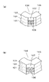
図1(a)は、本発明の水晶発振器用パッケージおよび水晶発振器の実施の形態の一例を示す上面図であり、図1(b)は(a)の側面図(A−A線における部分断面図)である。図1において、101は絶縁層、105は絶縁基体、106は電極端子、107は溝部である。複数の絶縁層101が積層されてなり、上面に凹部104を有する直方体状の絶縁基体105の隣り合う側面の間に溝部107が形成されているとともに、その溝部107の表面に電極端子106が形成されて本発明の水晶発振器用パッケージが基本的に構成されている。この絶縁基体105の凹部104内に水晶振動子102および半導体素子103が収容されるとともに、凹部104が蓋体108等で気密封止されることにより、携帯電話やコンピュータ等の各種電子機器において部品として使用される水晶発振器が作製される。
FIG. 1A is a top view showing an example of an embodiment of a crystal oscillator package and a crystal oscillator according to the present invention, and FIG. 1B is a side view of FIG. Figure). In FIG. 1, 101 is an insulating layer, 105 is an insulating substrate, 106 is an electrode terminal, and 107 is a groove. A plurality of
なお、図1では、絶縁基体105の上面に金属枠体109が接合され、この金属枠体109を介して蓋体108が絶縁基体105に接合されている例を示している。また図1(a)では、凹部104内の状態を示すために、蓋体108および金属枠体109を省略して示している。
FIG. 1 shows an example in which a
水晶振動子102は、いわゆるATカットやSCカット等の水晶板に接続用電極(図示せず)と励振電極(図示せず)とが設けられてなり、外部の電気回路(図示せず)から接続用電極を介して励振電極に電力が供給されて、所定の周波数で発振する。また、半導体素子103は、少なくとも発振回路(図示せず)と温度補償回路(図示せず)とを備える集積回路素子であり、水晶振動子102から伝送された発振の信号に応じて基準周波数の信号を外部の電気回路に供給する機能、およびその信号に対する温度補償を行なう機能を有している。基準信号は、例えば携帯電話やコンピュータ等の電子機器において時間や周波数等の基準信号として使用される。
The
このような水晶発振器は、水晶振動子102の接続用電極を介して供給される電力により水晶振動子102が振動して時間や周波数の基準となる信号を発振し、この信号が、水晶振動子102と電気的に接続された半導体素子103の発振回路を通じて外部の電気回路に供給される。この際に、あらかじめ水晶振動子102の特性に応じた温度補償情報を半導体素子103の情報書き込み用電極(図示せず)を介して書き込んでおくことにより、信号に対する温度補償を行なうことが可能な、温度補償型の水晶発振器(TCXO:Temperature Compensated Crystal Oscillator)が構成される。
In such a crystal oscillator, the
絶縁基体105は、全体の形状が直方体状であり、上面等の表面の中央部に凹部104を有している。凹部104は、水晶振動子102および半導体素子103を収容して気密封止するための部位であり、収容する水晶振動子102や半導体素子103の形状および寸法等に応じた形状(平面視で長方形状等)および寸法を有している。
The insulating
絶縁層101(絶縁基体105)を構成する材料としては、セラミック材料や樹脂材料,セラミック材料と樹脂材料との複合材料等の電気絶縁性材料等が挙げられる。ここで、セラミック材料とは、酸化アルミニウム質焼結体やガラスセラミック焼結体,窒化アルミニウム質焼結体,炭化珪素質焼結体,窒化珪素質焼結体,ムライト質焼結体等であり、樹脂材料とは、エポキシ樹脂やポリイミド樹脂,アクリル樹脂,フェノール樹脂等の熱硬化型または紫外線硬化型の樹脂である。 Examples of the material constituting the insulating layer 101 (insulating base 105) include a ceramic material, a resin material, and an electrically insulating material such as a composite material of a ceramic material and a resin material. Here, the ceramic material includes an aluminum oxide sintered body, a glass ceramic sintered body, an aluminum nitride sintered body, a silicon carbide sintered body, a silicon nitride sintered body, a mullite sintered body, and the like. The resin material is a thermosetting or ultraviolet curable resin such as an epoxy resin, a polyimide resin, an acrylic resin, or a phenol resin.
ここで、絶縁基体105を構成する材料として酸化アルミニウム質焼結体を採用した場合における絶縁基体105の作製方法の一例について説明する。まず、酸化アルミニウム(アルミナ)や酸化カルシウム,酸化マグネシウム等の原料粉末を有機溶剤やバインダなどとともにドクターブレード法等の成形手法によりシート状に成形して、複数のセラミックグリーンシートを作製する。次に、作製したセラミックグリーンシートを所定寸法まで積層して積層体とした上で、所定の焼成温度(例えば1300〜1600℃程度)で焼成する。以上のようにして、絶縁基体105が作製される。なお、積層された個々のセラミックグリーンシートがそれぞれ絶縁層101を構成している。
Here, an example of a method for manufacturing the insulating
絶縁基体105の隣り合う側面の間の角部に上下方向に形成された溝部107、およびその溝部107を絶縁層101の少なくとも1層において埋めて形成された電極端子106は、凹部104内に収容される半導体素子103の温度補償情報書き込み用電極(以下、書き込み用電極という)(図示せず)と電気的に接続され、外部の電気回路から温度補償情報を半導体素子103に書き込むためのものである。
A
電極端子106と半導体素子103の情報書き込み用電極との電気的な接続は、例えば、絶縁基体105に電極端子106から凹部104の内側にかけて配線導体(図示せず)を形成しておき、この配線導体110のうち凹部104の内側に位置している部分と情報書き込み用電極とをボンディングワイヤ等の導電性接続材(図示せず)を介して電気的に接続することにより行なわれる。
For the electrical connection between the
本発明の水晶発振器用パッケージにおいて、電極端子106は、例えば図2(a)または
(b)に示すように、絶縁基体105の角部の絶縁層101の少なくとも1層において、溝部107を埋めて溝部107の開口面よりも外側に凸状に突出している。なお、図2(a)および(b)は、それぞれ本発明の水晶発振器用パッケージの要部を拡大した一例を示す要部拡大斜視図である。図2において図1と同様の部位には同様の符号を付している。また、図2においては、わかりやすいように蓋体108および金属枠体109等を省略して示している。
In the crystal oscillator package of the present invention, the
本発明の水晶発振器用パッケージは、このような構造としたことから、水晶発振器用パッケージが小型化して絶縁基体105の凹部104を取り囲む枠状の部分の幅が狭くなっても、絶縁基体105の外表面に電極端子106を形成することができる。また、この電極端子106は、溝部107の開口面よりも外側に突出しているので、半導体素子103の水晶振動子102に対する温度補償のデータ(情報)を書き込むために用いられるプローブピン(図示せず)を、溝部107の内部にまで入り込ませることなく押し当てることができる。また、この電極端子106は、直方体状の絶縁基体105の角部に位置するため、絶縁基体105が小型化してもその位置の認識が容易である。
Since the crystal oscillator package of the present invention has such a structure, even if the crystal oscillator package is downsized and the width of the frame-shaped portion surrounding the
したがって、このような本発明の水晶発振器用パッケージを用いた本発明の水晶発振器によれば、小型化が進んだとしても、プローブピンを電極端子106に押し当てて半導体素子103への情報の書き込み等を容易に行なうことが可能である。
Therefore, according to the crystal oscillator of the present invention using the package for the crystal oscillator of the present invention, even if the miniaturization is advanced, the probe pin is pressed against the
電極端子106は、例えばタングステンやモリブデン,マンガン,銅,銀,パラジウム,金等の金属材料からなり、メタライズ法やめっき法等により形成されている。ここで、電極端子106を構成する金属材料としてタングステンを選択し、メタライズ法で形成する場合の一例について説明する。
The
まず、タングステンの粉末を有機溶剤やバインダなどとともに混練して、タングステンのメタライズペーストを作製する。次に、絶縁基体105となるセラミックグリーンシートの角部に溝部107を、金型を用いた打ち抜き加工等の加工方法で形成する。そして、作製したメタライズペーストをセラミックグリーンシートの切り欠き内に充填するとともに金型等を用いて所定の電極端子106の形状に成形し、その後、セラミックグリーンシートと同時焼成する。このようにして、電極端子106が作製される。
First, tungsten powder is kneaded with an organic solvent, a binder, or the like to produce a tungsten metallized paste. Next, the
電極端子106は、以上のようにセラミックグリーンシート(個々の絶縁層101)を単位にして形成されていること、および少なくとも1層分の高さがあればプローブピンを押し当てる上で十分であることから、少なくとも1層の絶縁層101の角部に形成されている。なお、絶縁層101の1層の厚さ(電極端子106の高さ)は、例えば、一般的なATカットやSCカットの水晶板が用いられてなる水晶振動子102が収容された、携帯電話において使用される水晶発振器を構成する水晶発振器用パッケージの場合であれば、約0.1〜0.5mm程度である。このような絶縁層101が3〜7層程度積層されて、厚さが約0.5〜1.5mm程度の絶縁基体105が形成されている。
The
また、電極端子106を半導体素子103の情報書き込み電極に電気的に接続するための配線導体も、電極端子106と同様の金属材料を用いて形成することができる。この配線導体も、電極端子106を形成するのと同様のメタライズペーストをセラミックグリーンシートの表面にスクリーン印刷法で所定パターンに印刷することにより形成することができる。
A wiring conductor for electrically connecting the
なお、このような電極端子106を有する絶縁基体105(水晶発振器用パッケージ)は、例えば図3に示すように、いわゆる多数個取り基板を個片に分割する方法で製作することもできる。図3(a)は、本発明の水晶発振器用パッケージを多数個取り基板の形態で製作する場合の一例を示す平面図であり、(b)は(a)の要部を拡大して示す要部拡大平面図である。図3において図1および図2と同様の部位には同様の符号を付している。
The insulating base 105 (quartz oscillator package) having
多数個取り基板は、水晶発振器用パッケージとなる複数個の基板領域122が母基板121に縦横の並びに配列されて形成されている。母基板121の上面や下面には、基板領域122の境界に分割ライン113が形成され、この分割ライン113において母基板121をダイシング加工等の方法で分割することにより、複数個の水晶発振器用パッケージが製作される。
The multi-chip substrate is formed by arranging a plurality of
母基板121は、個片の絶縁基体105と同様に複数の絶縁層(図示せず)が積層されてなり、基板領域122(絶縁層)の角部、つまり分割ライン113が交差する部分に溝部107となる貫通孔111が形成され、貫通孔111には電極端子106となる金属材料が被着されている。
The
この場合、絶縁層の角部に電極端子106となる部位を形成するためには、例えば、まず図4(a)に示したように、絶縁層となるセラミックグリーンシート114を準備し、分割ライン113が交差する部分に基板領域122の角部を切り欠くように溝部107となる貫通孔111を形成して、この貫通孔111に電極端子106となるメタライズペースト112を充填する。次に図4(b)に示すように、メタライズペースト112を充填した貫通孔111の中央部分から貫通孔111に隣接する基板領域122の外縁部分にかけて、十字状に打ち抜き加工を施す。以上により、図4(c)に示すように、個々の基板領域122(絶縁層)の角部に、開口面から電極端子106となるメタライズペーストが突出するように充填された、溝部107となる貫通孔111が形成される。
In this case, in order to form a portion to be the
このセラミックグリーンシート114を積層するとともに焼成することにより多数個取り基板が作製され、この多数個取り基板を分割ライン113に沿って分割することにより、個片の水晶発振器用パッケージが製作される。
The ceramic
なお、この場合には、4つの絶縁基体105の角部となる1箇所の貫通孔111を、十字状の1つのパンチで打ち抜き加工すれば、一度に4つの電極端子106を形成することができ、小さい電極端子106を形成する作業の生産性を高めることができる。
In this case, four
なお、図4(a)〜(c)は、それぞれ本発明の水晶発振器用パッケージを製作する工程の一例を工程順に示す要部拡大平面図である。図4において、図1および図2と同様の部位には同様の符号を付している。また、図4では、絶縁基体105の角部の状態をわかり易くするために、分割ライン113を破線で示している。
4A to 4C are main part enlarged plan views showing an example of a process for manufacturing the crystal oscillator package of the present invention in the order of processes. 4, parts similar to those in FIGS. 1 and 2 are given the same reference numerals. Further, in FIG. 4, the
なお、この方法で製作された水晶発振器用パッケージは、溝部107および電極端子106の形状が、図2(a)に示すような、溝部107の外側縁と絶縁基体105の側面との間に凹状の段差を有する形状になる。
In the crystal oscillator package manufactured by this method, the shape of the
この、図2(a)に示すような形状の場合には、次のような効果を得ることもできる。すなわち、電極端子106は、水晶発振器として完成した後においてコンピュータ等の外部電子機器の水晶振動子102の特性を高安定化,高精度化するための情報を半導体素子103に書き込むために用いられるものであるが、半導体素子103に情報を書き込んだ後も絶縁基体105の角部にそのまま露出して残るものである。そのため、電極端子106の表面には金めっきやニッケルめっき等で被覆されている。
In the case of the shape shown in FIG. 2A, the following effects can be obtained. In other words, the
このめっきを多数個取り基板に対して施す際に、個片の水晶発振器用パッケージにおいて露出する電極端子106の全面が、隣り合う基板領域122の間の分割ライン113に接しないことから、電極端子106の切断面(めっきが被着されない部分)が存在しない。そのため、電極端子106の露出する全面をより有効にめっき層で被覆することができる。よって、水晶発振器が使用される環境において、電極端子106の腐食やマイグレーション等を抑制できるという効果を得ることができる。
Since the entire surface of the
この水晶発振器用パッケージは、凹部104に半導体素子103を収容するとともに、その情報書き込み用電極を電極端子106に電気的に接続させた後、電極端子106にコンピュータ等の電子機器が備える外部の電気回路と接続されたプローブピンを接触させて、半導体素子103に水晶振動子102に対する温度補償の情報の書き込み等が行なわれる。例えば、外部の電気回路から電極端子106を介して半導体素子103の情報書き込み用電極に温度補償情報等の電子情報を入力することにより、半導体素子103のメモリ内容等を書き換えることが可能となり、水晶振動子102の振動特性や水晶発振器の使用環境等に対応して正確に温度補償することができるように、半導体素子103の機能(補正演算の機能等)を調整することができる。
In this crystal oscillator package, the
この実施の形態の例においては、絶縁基体105の凹部104に水晶振動子102や半導体素子103などを収容した後、凹部104が、いわゆるシーム溶接で接合された蓋体108により気密封止されている。すなわち、絶縁基体105の上面にあらかじめろう付け等の方法で接合された金属枠体109に金属からなる蓋体108を載置して、この蓋体108の外周縁にシーム溶接機の一対のローラー電極を接触させながら転動させるとともに、このローラー電極間に溶接のための大電流を流す。この抵抗発熱により、ローラー電極と蓋体108との接触部を高温とし、この熱によって金属枠体109に蓋体108をシーム溶接することによって、気密封止が行なわれる。
In the example of this embodiment, after accommodating the
なお、このタイプの水晶発振器においては、通常は金属枠体109および蓋体108の表面にあらかじめニッケルめっき膜および金めっき膜が被着されており、シーム溶接の熱によりこれらのニッケルめっき膜および金めっき膜の一部を溶融させることによって、金属枠体109と蓋体108とが溶接される。この場合、金属枠体109および蓋体108としては、溶接法に適するように、鉄−ニッケル合金や鉄−ニッケル−コバルト合金等の金属材料からなるものが使用される。
In this type of crystal oscillator, normally, a nickel plating film and a gold plating film are applied in advance to the surfaces of the
このようにシーム溶接で蓋体108が絶縁基体105(金属枠体109)に接合される場合に、本発明の水晶発振器用パッケージは次のような点で有効である。すなわち、絶縁基体105の外側面に従来技術のように溝部107が形成されていないため、水晶発振器用パッケージが小型化しても絶縁基体105の凹部104を囲む枠状の部分(上面に金属枠体109を介して蓋体108がシーム溶接される部分)の、平面視したときの辺部分における幅がこの溝部107により狭くならない。そのため、絶縁基体105の機械的な強度を確保する上で効果があり、蓋体108を水晶発振器用パッケージの上面にシーム溶接する際に絶縁基体105に熱衝撃が加わった場合においても、絶縁基体105にクラックが発生することを有効に抑制することができる。
As described above, when the
また、本発明の水晶発振器用パッケージによれば、電極端子106が、平面視で円弧状または楕円弧状の形状で溝部107の開口面から突出している場合には、電極端子106の突出部分に、欠け等の不具合が生じやすい絶縁基体105の角部分がないので、例えばプローブピンとの接触等の際に電極端子106に欠け等の機械的な破壊が生じることをより効果的に抑制することができる。
Further, according to the crystal oscillator package of the present invention, when the
また、電極端子106のうち、主にプローブピンが当たる中央部分における厚みを相対的に厚く確保することが容易であるので、プローブピンからの機械的な衝撃を電極端子106により吸収することができる。よって、プローブピンの衝撃により絶縁基体105に欠け等の機械的な破壊が生じることをより効果的に抑制することができる。さらに、絶縁層101の少なくとも1層の角部に上下方向に形成された溝部107による絶縁基体105の枠体の強度低下を補うことができるという効果もある。
In addition, since it is easy to ensure a relatively large thickness at the central portion of the
また、溝部107の開口面よりも外側に突出している電極端子106にプローブピン(符号なし)を押し当てる際に、例えば電極端子106の表面が平坦な場合に比べて、プローブピンを押し当てる角度が多少ずれたとしても、電気的接続の安定性をより確実に確保できる。
In addition, when the probe pin (not indicated) is pressed against the
つまり、電極端子106が平面視で円弧状または楕円弧状の形状で突出している場合には、プローブピンを押し当てる角度が多少ずれたとしても、円弧または楕円弧の接線方向に対してほぼ直角にプローブピンが電極端子106に接しやすい。そのため、プローブピンが電極端子106の表面で滑るようなことを効果的に抑制することができる。
In other words, when the
ここで、プローブピンは、一般的な棒状(先端が円錐状のもの等)に限らず、先端(接触面)が平らな円盤状のものや、その円盤状の表面(電極端子106に押し当てる側)に複数の突起が配列された形状としてもよい。この場合には、溝部107の開口面から突出した電極端子106の円弧状等の表面にプローブピンの先端を押し当てることが容易であるため、プローブピンと電極端子106との接触をより容易に行なうことができる。
Here, the probe pin is not limited to a general rod shape (such as a conical tip), but is a disk having a flat tip (contact surface) or a disk-shaped surface (pressing against the electrode terminal 106). A plurality of protrusions may be arranged on the side). In this case, since it is easy to press the tip of the probe pin against the arc-shaped surface of the
また、プローブピンの先端(接触面)を平面視でU字状として、絶縁基体105の角部分を水平方向に挟み込むようにして電極端子106にプローブピンを接触させても、水晶発振器用パッケージとなる絶縁基体105が小型化した場合にプローブピンと電極端子106との接触を容易に行なうことが可能となる。
Even if the tip (contact surface) of the probe pin is U-shaped in plan view and the probe pin is brought into contact with the
また、実際に温度補償情報を書き込む作業を想定した場合、水晶発振器用パッケージの外周部をチャッキングして位置固定してしまえば、電極端子106が平面視で円弧状または楕円弧状の形状等で溝部107の開口面から突出している場合には、前述のように水平方向におけるプローブピンを押し当てる角度の許容範囲が広い。よって、より正確に水晶振動子102について温度補償することができるように、プローブピンを電極端子106に押し当てて半導体素子103に情報を書き込み、半導体素子103の機能を調整することができる。
Assuming that temperature compensation information is actually written, if the outer periphery of the crystal oscillator package is chucked and fixed in position, the
さらに、電極端子106が平面視で円弧状または楕円弧状の形状で溝部107の開口面から突出している場合には、絶縁層101の角部に電極端子106を形成する際に、前述のようにメタライズペーストを金型で打ち抜いて加工する場合に、バリやカケ等の不具合が生じやすい角部がないので、金型等での打ち抜きによる加工性をより良好なものとすることができる。
Further, when the
本発明の水晶発振器は、上記いずれかの構成の水晶発振器用パッケージの凹部104内に、水晶振動子102と、水晶振動子102に対する温度補償を行なう半導体素子103とが収容されており、半導体素子103の水晶振動子102に対する温度補償の情報書き込み用電極が電極端子106と電気的に接続されている。このような構成としたことから、内部に収納する水晶振動子102および半導体素子103において、水晶振動子102に対する温度補償を行なう半導体素子103の情報書き込み用電極に、外部から確実かつ高精度に情報書き込みを行なうことができ、所定の性能で安定して動作させることが可能な、高信頼性で、かつ小型の水晶発振器を提供することができる。
In the crystal oscillator of the present invention, the
水晶発振器は、例えば絶縁基体105に凹部104から下面にかけて形成された配線導体110を介して外部の電気回路と電気的に接続される。配線導体110のうち凹部104内に露出した部分に水晶振動子102の接続用電極が導電性接着剤(符号なし)等を介して電気的,機械的に接続されるとともに、絶縁基体105の下面に露出した部分が外部の電気回路とはんだ等の接合材を介して接合されることにより、配線導体110を介して水晶振動子102と外部の電気回路とが電気的に接続される。なお、この配線導体110も、前述した電極端子106と凹部104の内側との間を導通する配線導体と同様の金属材料を用い、同様の方法で形成することができる。
The crystal oscillator is electrically connected to an external electric circuit through a
水晶発振器は、例えば前述したように絶縁基体105の厚さが0.5〜1.5mm程度であり、平面視したときの外形寸法が2.0〜4.0mm×1.6〜3.2mm程度の長方形状である。
For example, as described above, the quartz oscillator has a rectangular shape in which the thickness of the insulating
この絶縁基体105の角部に、例えば半径が約0.15〜0.4mm程度の円弧状の溝部107が形成され、絶縁基体105を構成する絶縁層101の少なくとも1層におけるその溝部107の開口面から、例えば平面視で半径が約0.1〜0.3mmの円弧状の形状で突出して、電極端子106が形成されている。電極端子106は、少なくとも絶縁層101の1層分の高さ(その絶縁層101の厚さに相当する)を有し、前述したような、形状および寸法の絶縁基体105(ATカットやSCカットの水晶振動子102が収容されるもの)の場合であれば、個々の絶縁層101の厚さが約0.1〜0.5mmであるので、0.1〜0.5mm程度の高さである。
An
具体的な例として、酸化アルミニウム質焼結体からなる厚さが0.2mmの絶縁層101を5層積層してなる絶縁基体105の角部に、半径が約0.3mmの円弧状の溝部107を形成し、その溝部107の開口面から平面視で半径が約0.2mmの円弧状の形状で突出した、高さが0.3mmの電極端子106を形成した水晶発振器用パッケージについて、半導体素子103に対して温度補償情報の書き込みを行なった。書き込まれた温度補償情報の適否は、水晶発振器の温度環境を−10℃〜+50℃の範囲で変化させて周波数の変動の大きさを見ることにより確認した。
As a specific example, an
なお、水晶振動子102はSCカット型であり、凹部104は、絶縁基体105の上面にろう付けした、鉄−ニッケル−コバルト合金からなる金属枠体109に、鉄−ニッケル−コバルト合金からなる蓋体108をシーム溶接で接合することにより気密封止した。
The
その結果、この例の水晶発振器においては、−10℃〜+50℃における発振周波数(f)の変動(温度特性Δf/f)が約±0.7×10−6〜0.9×10−6の範囲であった。これは、目標とした±1.0×10−6以内の変動を満足する値であり、半導体素子103に水晶振動子102に対する温度補償の情報が正しく書き込まれて有効に温度補償が行なわれたことが確認できた。なお、温度補償を行なわない場合の周波数の変動は、他の条件が同じとき、約50×10−6であった。
As a result, in the crystal oscillator of this example, the fluctuation (temperature characteristic Δf / f) of the oscillation frequency (f) at −10 ° C. to + 50 ° C. is in the range of about ± 0.7 × 10 −6 to 0.9 × 10 −6. It was. This is a value that satisfies the target variation within ± 1.0 × 10 −6 , and the temperature compensation information for the
なお、本発明は、上述の実施の形態の例に限定されるものではなく、種々の変形が可能である。例えば、絶縁基体105は、前述の例では3層の絶縁層101を積層したものを示したが、4層以上の絶縁層101を積層することにより形成されていてもよい。また、電極端子106は、図2の例では絶縁基体105の溝部107の開口面よりも外側に突出して平面視で左右対称となるように円弧状または楕円弧状の形状に形成したが、プローブピンを接触させる角度を考慮して、左右非対称となるような楕円弧状等の形状としてもよい。さらに、電極端子106は、前述の例では1層の絶縁層101に対応させて形成したものを示したが、2層以上の絶縁層101の角部に連続して形成してもよい。さらに、絶縁基体105の上面に金属枠体109が接合され、この金属枠体109を介して金属からなる蓋体108が絶縁基体105に接合されている例を示したが、蓋体108を絶縁基体105の上面にあらかじめ形成された金属面(例えば、配線導体110と同様の金属材料を用い、同様の方法で形成したメタライズ層)に直接溶接する水晶発振器用パッケージおよび水晶発振器としてもよい。
In addition, this invention is not limited to the example of the above-mentioned embodiment, A various deformation | transformation is possible. For example, in the above example, the insulating
101・・・・絶縁層
102・・・・水晶振動子
103・・・・半導体素子
104・・・・凹部
105・・・・絶縁基体
106・・・・電極端子
107・・・・溝部
108・・・・蓋体
109・・・・金属枠体
110・・・・配線導体
111・・・・貫通孔
112・・・・メタライズペースト
113・・・・分割ライン
114・・・・セラミックグリーンシート
121・・・・多数個取り基板
122・・・・基板領域
101 ・ ・ ・ ・ Insulating layer
102 ・ ・ ・ ・ Quartz crystal unit
103 ・ ・ ・ ・ Semiconductor element
104 ・ ・ ・ ・ Recess
105 ・ ・ ・ ・ Insulating substrate
106 ・ ・ ・ ・ Electrode terminal
107 ・ ・ ・ ・ Groove
108 ・ ・ ・ ・ Cover body
109 ... Metal frame
110 ... Wiring conductor
111 ... Through hole
112 ... Metalized paste
113 ... Dividing line
114 ・ ・ ・ ・ Ceramic green sheet
121 ・ ・ ・ ・ Multi-piece substrate
122 ・ ・ ・ ・ Board area
Claims (3)
Priority Applications (1)
| Application Number | Priority Date | Filing Date | Title |
|---|---|---|---|
| JP2008132753A JP5252992B2 (en) | 2008-05-21 | 2008-05-21 | Crystal oscillator package and crystal oscillator |
Applications Claiming Priority (1)
| Application Number | Priority Date | Filing Date | Title |
|---|---|---|---|
| JP2008132753A JP5252992B2 (en) | 2008-05-21 | 2008-05-21 | Crystal oscillator package and crystal oscillator |
Publications (2)
| Publication Number | Publication Date |
|---|---|
| JP2009284125A JP2009284125A (en) | 2009-12-03 |
| JP5252992B2 true JP5252992B2 (en) | 2013-07-31 |
Family
ID=41454130
Family Applications (1)
| Application Number | Title | Priority Date | Filing Date |
|---|---|---|---|
| JP2008132753A Expired - Fee Related JP5252992B2 (en) | 2008-05-21 | 2008-05-21 | Crystal oscillator package and crystal oscillator |
Country Status (1)
| Country | Link |
|---|---|
| JP (1) | JP5252992B2 (en) |
Families Citing this family (3)
| Publication number | Priority date | Publication date | Assignee | Title |
|---|---|---|---|---|
| JP5262348B2 (en) * | 2008-06-27 | 2013-08-14 | 株式会社大真空 | Base assembly and method for manufacturing piezoelectric device using base assembly |
| JP5262347B2 (en) * | 2008-06-27 | 2013-08-14 | 株式会社大真空 | Base assembly and method for manufacturing piezoelectric device using base assembly |
| JP5731880B2 (en) * | 2010-10-15 | 2015-06-10 | 日本電波工業株式会社 | Piezoelectric device and method for manufacturing piezoelectric device |
Family Cites Families (8)
| Publication number | Priority date | Publication date | Assignee | Title |
|---|---|---|---|---|
| JPH09130145A (en) * | 1995-10-31 | 1997-05-16 | Kinseki Ltd | Piezoelectric oscillator |
| JPH1197931A (en) * | 1997-09-25 | 1999-04-09 | Citizen Watch Co Ltd | Oscillator |
| JP4269412B2 (en) * | 1999-06-23 | 2009-05-27 | エプソントヨコム株式会社 | Piezoelectric oscillator |
| JP4378980B2 (en) * | 2002-03-25 | 2009-12-09 | セイコーエプソン株式会社 | Electronic components with control terminals |
| JP4600663B2 (en) * | 2004-12-07 | 2010-12-15 | セイコーエプソン株式会社 | Temperature compensated piezoelectric oscillator |
| JP4645393B2 (en) * | 2005-09-27 | 2011-03-09 | エプソントヨコム株式会社 | Surface mount type piezoelectric oscillator and electronic component unit |
| JP4244053B2 (en) * | 2006-06-16 | 2009-03-25 | エプソントヨコム株式会社 | Electronic module with piezoelectric device |
| JP2008014724A (en) * | 2006-07-04 | 2008-01-24 | Citizen Holdings Co Ltd | Electronic circuit device, package with built-in electronic circuit, and angular velocity sensor |
-
2008
- 2008-05-21 JP JP2008132753A patent/JP5252992B2/en not_active Expired - Fee Related
Also Published As
| Publication number | Publication date |
|---|---|
| JP2009284125A (en) | 2009-12-03 |
Similar Documents
| Publication | Publication Date | Title |
|---|---|---|
| JP2011147054A (en) | Electronic apparatus, and method of manufacturing the same | |
| JP2006279872A (en) | Piezoelectric vibrator, manufacturing method thereof, and manufacturing method of piezoelectric oscillator using the piezoelectric vibrator | |
| JP4899519B2 (en) | Surface mount type piezoelectric oscillator | |
| JP5252992B2 (en) | Crystal oscillator package and crystal oscillator | |
| JP2009033613A (en) | Lid body aggregate, piezoelectric vibration device using the lid body aggregate concerned, and manufacturing method of the piezoelectric vibration device | |
| JP5097929B2 (en) | Manufacturing method of electronic parts | |
| JP6818581B2 (en) | Electronic component storage packages, electronic devices and electronic modules | |
| JP5101093B2 (en) | Piezoelectric oscillator and manufacturing method thereof | |
| JP2005268257A (en) | Electronic component storage package and electronic device | |
| JP4380419B2 (en) | Manufacturing method of electronic device | |
| JP4332037B2 (en) | Electronic component storage package and electronic device | |
| JP4144036B2 (en) | Electronic component package and piezoelectric vibration device using the electronic component package | |
| JP5005336B2 (en) | Method for manufacturing piezoelectric oscillator | |
| JP4549158B2 (en) | Method for manufacturing crystal oscillator | |
| JP2009239475A (en) | Surface mounting piezoelectric oscillator | |
| JP4585908B2 (en) | Method for manufacturing piezoelectric device | |
| JP2008289055A (en) | Sheet substrate and method of manufacturing piezoelectric vibration device employing sheet substrate | |
| JP4472445B2 (en) | Method for manufacturing piezoelectric oscillator | |
| JP6391235B2 (en) | Crystal device | |
| JP4113459B2 (en) | Manufacturing method of temperature compensated crystal oscillator | |
| JP5220584B2 (en) | Piezoelectric oscillator and manufacturing method thereof | |
| JP2007180885A (en) | Piezoelectric device | |
| JP4373309B2 (en) | Package for electronic components | |
| JP4916805B2 (en) | Piezoelectric oscillator | |
| JP2004297209A (en) | Surface mount type piezoelectric oscillator |
Legal Events
| Date | Code | Title | Description |
|---|---|---|---|
| A621 | Written request for application examination |
Free format text: JAPANESE INTERMEDIATE CODE: A621 Effective date: 20101215 |
|
| A131 | Notification of reasons for refusal |
Free format text: JAPANESE INTERMEDIATE CODE: A131 Effective date: 20121106 |
|
| A521 | Written amendment |
Free format text: JAPANESE INTERMEDIATE CODE: A523 Effective date: 20121208 |
|
| TRDD | Decision of grant or rejection written | ||
| A01 | Written decision to grant a patent or to grant a registration (utility model) |
Free format text: JAPANESE INTERMEDIATE CODE: A01 Effective date: 20130319 |
|
| A61 | First payment of annual fees (during grant procedure) |
Free format text: JAPANESE INTERMEDIATE CODE: A61 Effective date: 20130416 |
|
| R150 | Certificate of patent or registration of utility model |
Ref document number: 5252992 Country of ref document: JP Free format text: JAPANESE INTERMEDIATE CODE: R150 Free format text: JAPANESE INTERMEDIATE CODE: R150 |
|
| FPAY | Renewal fee payment (event date is renewal date of database) |
Free format text: PAYMENT UNTIL: 20160426 Year of fee payment: 3 |
|
| LAPS | Cancellation because of no payment of annual fees |