JP5248062B2 - Directional backlight, display device, and stereoscopic image display device - Google Patents
Directional backlight, display device, and stereoscopic image display device Download PDFInfo
- Publication number
- JP5248062B2 JP5248062B2 JP2007218499A JP2007218499A JP5248062B2 JP 5248062 B2 JP5248062 B2 JP 5248062B2 JP 2007218499 A JP2007218499 A JP 2007218499A JP 2007218499 A JP2007218499 A JP 2007218499A JP 5248062 B2 JP5248062 B2 JP 5248062B2
- Authority
- JP
- Japan
- Prior art keywords
- wiring pattern
- liquid crystal
- electrode
- display device
- light
- Prior art date
- Legal status (The legal status is an assumption and is not a legal conclusion. Google has not performed a legal analysis and makes no representation as to the accuracy of the status listed.)
- Expired - Fee Related
Links
Images


Classifications
-
- G—PHYSICS
- G09—EDUCATION; CRYPTOGRAPHY; DISPLAY; ADVERTISING; SEALS
- G09G—ARRANGEMENTS OR CIRCUITS FOR CONTROL OF INDICATING DEVICES USING STATIC MEANS TO PRESENT VARIABLE INFORMATION
- G09G3/00—Control arrangements or circuits, of interest only in connection with visual indicators other than cathode-ray tubes
- G09G3/001—Control arrangements or circuits, of interest only in connection with visual indicators other than cathode-ray tubes using specific devices not provided for in groups G09G3/02 - G09G3/36, e.g. using an intermediate record carrier such as a film slide; Projection systems; Display of non-alphanumerical information, solely or in combination with alphanumerical information, e.g. digital display on projected diapositive as background
- G09G3/003—Control arrangements or circuits, of interest only in connection with visual indicators other than cathode-ray tubes using specific devices not provided for in groups G09G3/02 - G09G3/36, e.g. using an intermediate record carrier such as a film slide; Projection systems; Display of non-alphanumerical information, solely or in combination with alphanumerical information, e.g. digital display on projected diapositive as background to produce spatial visual effects
-
- G—PHYSICS
- G02—OPTICS
- G02B—OPTICAL ELEMENTS, SYSTEMS OR APPARATUS
- G02B30/00—Optical systems or apparatus for producing three-dimensional [3D] effects, e.g. stereoscopic images
- G02B30/20—Optical systems or apparatus for producing three-dimensional [3D] effects, e.g. stereoscopic images by providing first and second parallax images to an observer's left and right eyes
- G02B30/26—Optical systems or apparatus for producing three-dimensional [3D] effects, e.g. stereoscopic images by providing first and second parallax images to an observer's left and right eyes of the autostereoscopic type
- G02B30/27—Optical systems or apparatus for producing three-dimensional [3D] effects, e.g. stereoscopic images by providing first and second parallax images to an observer's left and right eyes of the autostereoscopic type involving lenticular arrays
-
- G—PHYSICS
- G02—OPTICS
- G02F—OPTICAL DEVICES OR ARRANGEMENTS FOR THE CONTROL OF LIGHT BY MODIFICATION OF THE OPTICAL PROPERTIES OF THE MEDIA OF THE ELEMENTS INVOLVED THEREIN; NON-LINEAR OPTICS; FREQUENCY-CHANGING OF LIGHT; OPTICAL LOGIC ELEMENTS; OPTICAL ANALOGUE/DIGITAL CONVERTERS
- G02F1/00—Devices or arrangements for the control of the intensity, colour, phase, polarisation or direction of light arriving from an independent light source, e.g. switching, gating or modulating; Non-linear optics
- G02F1/01—Devices or arrangements for the control of the intensity, colour, phase, polarisation or direction of light arriving from an independent light source, e.g. switching, gating or modulating; Non-linear optics for the control of the intensity, phase, polarisation or colour
- G02F1/13—Devices or arrangements for the control of the intensity, colour, phase, polarisation or direction of light arriving from an independent light source, e.g. switching, gating or modulating; Non-linear optics for the control of the intensity, phase, polarisation or colour based on liquid crystals, e.g. single liquid crystal display cells
- G02F1/133—Constructional arrangements; Operation of liquid crystal cells; Circuit arrangements
- G02F1/1333—Constructional arrangements; Manufacturing methods
- G02F1/1335—Structural association of cells with optical devices, e.g. polarisers or reflectors
- G02F1/1336—Illuminating devices
- G02F1/133602—Direct backlight
- G02F1/133606—Direct backlight including a specially adapted diffusing, scattering or light controlling members
-
- G—PHYSICS
- G09—EDUCATION; CRYPTOGRAPHY; DISPLAY; ADVERTISING; SEALS
- G09G—ARRANGEMENTS OR CIRCUITS FOR CONTROL OF INDICATING DEVICES USING STATIC MEANS TO PRESENT VARIABLE INFORMATION
- G09G3/00—Control arrangements or circuits, of interest only in connection with visual indicators other than cathode-ray tubes
- G09G3/20—Control arrangements or circuits, of interest only in connection with visual indicators other than cathode-ray tubes for presentation of an assembly of a number of characters, e.g. a page, by composing the assembly by combination of individual elements arranged in a matrix no fixed position being assigned to or needed to be assigned to the individual characters or partial characters
- G09G3/34—Control arrangements or circuits, of interest only in connection with visual indicators other than cathode-ray tubes for presentation of an assembly of a number of characters, e.g. a page, by composing the assembly by combination of individual elements arranged in a matrix no fixed position being assigned to or needed to be assigned to the individual characters or partial characters by control of light from an independent source
- G09G3/3406—Control of illumination source
- G09G3/3413—Details of control of colour illumination sources
-
- G—PHYSICS
- G09—EDUCATION; CRYPTOGRAPHY; DISPLAY; ADVERTISING; SEALS
- G09G—ARRANGEMENTS OR CIRCUITS FOR CONTROL OF INDICATING DEVICES USING STATIC MEANS TO PRESENT VARIABLE INFORMATION
- G09G3/00—Control arrangements or circuits, of interest only in connection with visual indicators other than cathode-ray tubes
- G09G3/20—Control arrangements or circuits, of interest only in connection with visual indicators other than cathode-ray tubes for presentation of an assembly of a number of characters, e.g. a page, by composing the assembly by combination of individual elements arranged in a matrix no fixed position being assigned to or needed to be assigned to the individual characters or partial characters
- G09G3/34—Control arrangements or circuits, of interest only in connection with visual indicators other than cathode-ray tubes for presentation of an assembly of a number of characters, e.g. a page, by composing the assembly by combination of individual elements arranged in a matrix no fixed position being assigned to or needed to be assigned to the individual characters or partial characters by control of light from an independent source
- G09G3/36—Control arrangements or circuits, of interest only in connection with visual indicators other than cathode-ray tubes for presentation of an assembly of a number of characters, e.g. a page, by composing the assembly by combination of individual elements arranged in a matrix no fixed position being assigned to or needed to be assigned to the individual characters or partial characters by control of light from an independent source using liquid crystals
- G09G3/3611—Control of matrices with row and column drivers
- G09G3/3648—Control of matrices with row and column drivers using an active matrix
-
- H—ELECTRICITY
- H04—ELECTRIC COMMUNICATION TECHNIQUE
- H04N—PICTORIAL COMMUNICATION, e.g. TELEVISION
- H04N13/00—Stereoscopic video systems; Multi-view video systems; Details thereof
- H04N13/30—Image reproducers
- H04N13/302—Image reproducers for viewing without the aid of special glasses, i.e. using autostereoscopic displays
- H04N13/305—Image reproducers for viewing without the aid of special glasses, i.e. using autostereoscopic displays using lenticular lenses, e.g. arrangements of cylindrical lenses
-
- H—ELECTRICITY
- H04—ELECTRIC COMMUNICATION TECHNIQUE
- H04N—PICTORIAL COMMUNICATION, e.g. TELEVISION
- H04N13/00—Stereoscopic video systems; Multi-view video systems; Details thereof
- H04N13/30—Image reproducers
- H04N13/302—Image reproducers for viewing without the aid of special glasses, i.e. using autostereoscopic displays
- H04N13/31—Image reproducers for viewing without the aid of special glasses, i.e. using autostereoscopic displays using parallax barriers
- H04N13/312—Image reproducers for viewing without the aid of special glasses, i.e. using autostereoscopic displays using parallax barriers the parallax barriers being placed behind the display panel, e.g. between backlight and spatial light modulator [SLM]
-
- H—ELECTRICITY
- H04—ELECTRIC COMMUNICATION TECHNIQUE
- H04N—PICTORIAL COMMUNICATION, e.g. TELEVISION
- H04N13/00—Stereoscopic video systems; Multi-view video systems; Details thereof
- H04N13/30—Image reproducers
- H04N13/302—Image reproducers for viewing without the aid of special glasses, i.e. using autostereoscopic displays
- H04N13/32—Image reproducers for viewing without the aid of special glasses, i.e. using autostereoscopic displays using arrays of controllable light sources; using moving apertures or moving light sources
-
- H—ELECTRICITY
- H04—ELECTRIC COMMUNICATION TECHNIQUE
- H04N—PICTORIAL COMMUNICATION, e.g. TELEVISION
- H04N13/00—Stereoscopic video systems; Multi-view video systems; Details thereof
- H04N13/30—Image reproducers
- H04N13/349—Multi-view displays for displaying three or more geometrical viewpoints without viewer tracking
- H04N13/354—Multi-view displays for displaying three or more geometrical viewpoints without viewer tracking for displaying sequentially
Landscapes
- Engineering & Computer Science (AREA)
- Physics & Mathematics (AREA)
- General Physics & Mathematics (AREA)
- Multimedia (AREA)
- Signal Processing (AREA)
- Computer Hardware Design (AREA)
- Theoretical Computer Science (AREA)
- Chemical & Material Sciences (AREA)
- Optics & Photonics (AREA)
- Crystallography & Structural Chemistry (AREA)
- Nonlinear Science (AREA)
- Mathematical Physics (AREA)
- Liquid Crystal (AREA)
- Control Of Indicators Other Than Cathode Ray Tubes (AREA)
- Stereoscopic And Panoramic Photography (AREA)
- Testing, Inspecting, Measuring Of Stereoscopic Televisions And Televisions (AREA)
Description
本発明は、指向性バックライト、当該指向性バックライトを用いた表示装置及び立体画像表示装置に関する。 The present invention relates to a directional backlight, a display device using the directional backlight, and a stereoscopic image display device.
立体的な動画表示が可能な立体視画像表示装置、所謂3次元ディスプレイには、種々の方式が知られている。近年、特にフラットパネルタイプで、且つ、専用の眼鏡等を必要としない立体視画像表示方式に対する要望が高くなっている。直視型或いは投影型の液晶表示装置やプラズマ表示装置等のような画素位置が固定されている表示パネル(表示装置)の直前に表示パネルからの光線を制御して観測者に向ける視差発生手段を設置する方式が比較的容易に実現できる方式として知られている。 Various methods are known for stereoscopic image display devices capable of displaying a three-dimensional moving image, so-called three-dimensional displays. In recent years, there has been a growing demand for a stereoscopic image display method that is particularly a flat panel type and does not require dedicated glasses. A parallax generating means for controlling light rays from the display panel and directing it to the observer immediately before a display panel (display device) having a fixed pixel position, such as a direct-view or projection-type liquid crystal display device or plasma display device. It is known that the installation method can be realized relatively easily.
この視差発生手段は、一般的にはパララクスバリア或いは視差バリアとも称せられ、光線制御素子上の同一位置でも角度により異なる画像が見えるように光線を制御している。具体的には、左右視差(水平視差)のみを与える場合には、視差発生手段として、スリット或いはレンチキュラーシート(シリンドリカルレンズアレイ)が使用される。また、上下視差(垂直視差)も含める場合には、視差発生手段として、ピンホールアレイ或いはレンズアレイが使用される。 This parallax generating means is generally called a parallax barrier or a parallax barrier, and controls the light beam so that different images can be seen depending on the angle even at the same position on the light beam control element. Specifically, when only left and right parallax (horizontal parallax) is given, a slit or a lenticular sheet (cylindrical lens array) is used as the parallax generating means. In addition, when including vertical parallax (vertical parallax), a pinhole array or a lens array is used as the parallax generating means.
視差バリアを使用する方式には、さらに2眼式、多眼式、超多眼式(多眼式の超多眼条件)、インテグラルイメージング(以下、「IP方式」という)に分類される。これらの基本的な原理は、100年程度前に発明され立体写真に用いられてきたものと実質上同一である。 The system using the parallax barrier is further classified into a binocular system, a multi-view system, a super multi-view system (multi-view super multi-view condition), and an integral imaging (hereinafter referred to as “IP system”). These basic principles are substantially the same as those invented about 100 years ago and used in stereoscopic photography.
多眼或いは1次元IP方式(水平視差のみのIP方式)において、非特許文献1、特許文献1に示されているように視差・解像度・飛び出し量は、トレードオフの関係にあり、3つの特性とも十分なレベルにすることは困難とされている。そこで、光線の方向を時分割で変化させることで解像度を向上させる技術が特許文献2、3に提案されている。
In the multi-view or one-dimensional IP method (IP method with only horizontal parallax), as shown in Non-Patent Document 1 and Patent Document 1, the parallax, resolution, and pop-out amount are in a trade-off relationship and have three characteristics. Both are considered difficult to achieve. Therefore,
しかしながら、上述した従来の技術では、何れも光線方向数の増加と、時分割で切り替えが必要な光源数の減少とが十分両立し得ず、観測位置の変化に対応し難いという問題がある。 However, each of the above-described conventional techniques has a problem that an increase in the number of light beam directions and a decrease in the number of light sources that need to be switched in a time-sharing manner cannot be sufficiently compatible, and it is difficult to cope with changes in observation positions.
本発明は上記に鑑みてなされたものであって、単一の面光源のみを用いて、光線の方向数を増やすとともに、視域を広げることが可能な指向性バックライト、表示装置及び立体画像表示装置を提供することを目的とする。 The present invention has been made in view of the above, and uses only a single surface light source to increase the number of directions of light rays and to widen the viewing zone, a display device, and a stereoscopic image An object is to provide a display device.
上述した課題を解決し、目的を達成するために、本発明は、発光面の法線方向に輝度分布が集中する特性を有した面光源と、前記面光源の発光面に対向して配置された第1の透明基板と、前記第1の透明基板と対向して配置された第2の透明基板と、前記第1及び第2の透明基板間に形成され一方又は両方がストライプ状の配線パターンを有した、対向する一対の電極から構成される複数の電極対と、前記電極間に保持された液晶層と、前記第2の透明基板上に配置され前記電極対の配線パターンに応じた開口部を有する遮光層と、を備えた偏向素子部と、前記電極の各配線パターンへの電圧印加状態を複数通りに切り替え、各電圧印加状態において、前記電極対毎に当該電極対を構成する電極に印加する電圧値を個別的に制御することで、前記各開口部を通過する前記面光源からの光線が所定の位置に向かうよう制御する電圧制御手段と、を備える。 In order to solve the above-described problems and achieve the object, the present invention is arranged such that a surface light source having a characteristic that the luminance distribution is concentrated in the normal direction of the light emitting surface and the light emitting surface of the surface light source. A first transparent substrate, a second transparent substrate disposed opposite to the first transparent substrate, and a wiring pattern in which one or both are formed between the first and second transparent substrates. A plurality of electrode pairs configured by a pair of electrodes facing each other, a liquid crystal layer held between the electrodes, and an opening corresponding to the wiring pattern of the electrode pairs disposed on the second transparent substrate a light shielding layer having a section, a deflection device portion having a switch to plural kinds of voltage application state to the wiring pattern of the electrodes, the voltage applying condition, the electrodes constituting the electrode pair for each of said electrode pairs By individually controlling the voltage value applied to Serial and a voltage control means that light rays are controlled so that toward the predetermined position from the plane light source passing through each opening.
また、本発明は、発光面の法線方向に輝度分布が集中する特性を有した面光源と、前記面光源の発光面に対向して配置された第1の透明基板と、前記第1の透明基板と対向して配置された第2の透明基板と、前記第1及び第2の透明基板間に形成され一方又は両方がストライプ状の配線パターンを有した一対の電極と、前記電極間に保持された液晶層と、前記第2の透明基板上に配置され前記電極の配線パターンに応じた複数の開口部を有する遮光層と、を備えた偏向素子部と、前記偏向素子部と対向して配置され、マトリクス状に配置された表示画素に複数個のフィールド画像に分割された1フレーム分の画像を表示する液晶表示素子と、前記液晶表示素子に表示された各フィールド画像を所定の時間間隔毎に切り替える同期制御手段と、前記電極の各配線パターンへの電圧印加状態を前記同期制御手段の切り替えタイミングに応じて複数通りに切り替え、各電圧印加状態において、前記各配線パターンに印加する電圧値を個別的に制御することで、前記各開口部を通過し前記液晶表示素子を透過する前記面光源からの光線が所定の位置に向かうよう制御する電圧制御手段と、を備える。 The present invention also provides a surface light source having a characteristic that the luminance distribution is concentrated in the normal direction of the light emitting surface, a first transparent substrate disposed opposite to the light emitting surface of the surface light source, and the first A second transparent substrate disposed opposite to the transparent substrate, a pair of electrodes formed between the first and second transparent substrates, one or both of which has a stripe-shaped wiring pattern, and between the electrodes A deflecting element portion comprising: a held liquid crystal layer; and a light shielding layer disposed on the second transparent substrate and having a plurality of openings according to the wiring pattern of the electrodes; and facing the deflecting element portion And a liquid crystal display element for displaying an image for one frame divided into a plurality of field images on display pixels arranged in a matrix, and each field image displayed on the liquid crystal display element for a predetermined time. Synchronization control means for switching at intervals; By switching the voltage application state to each wiring pattern of the electrode in multiple ways according to the switching timing of the synchronization control means, and individually controlling the voltage value applied to each wiring pattern in each voltage application state Voltage control means for controlling the light from the surface light source that passes through the openings and passes through the liquid crystal display element to be directed to a predetermined position.
また、本発明は、発光面の法線方向に輝度分布が集中する特性を有した面光源と、前記面光源の発光面に対向して配置された第1の透明基板と、前記第1の透明基板と対向して配置された第2の透明基板と、前記第1及び第2の透明基板間に形成され一方又は両方がストライプ状の配線パターンを有した一対の電極と、前記電極間に保持された液晶層と、前記第2の透明基板上に配置され前記電極の配線パターンに応じた複数の開口部を有する遮光層と、を備えた偏向素子部と、前記偏向素子部と対向して配置され、マトリクス状に配置された表示画素に複数個のフィールド画像からなる立体表示のための要素画像アレイを表示する液晶表示素子と、前記液晶表示素子の前面又は背面に配置された視差発生手段と、前記電極の各配線パターンへの電圧印加状態を、前記各フィールド画像の表示に応じて、複数通りに切り替え、各電圧印加状態において、前記各配線パターンに印加する電圧値を個別的に制御することで、前記開口部を通過し前記液晶表示素子及び視差発生手段を透過する前記面光源からの光線が所定の位置に向かうよう制御する電圧制御手段と、を備える。 The present invention also provides a surface light source having a characteristic that the luminance distribution is concentrated in the normal direction of the light emitting surface, a first transparent substrate disposed opposite to the light emitting surface of the surface light source, and the first A second transparent substrate disposed opposite to the transparent substrate, a pair of electrodes formed between the first and second transparent substrates, one or both of which has a stripe-shaped wiring pattern, and between the electrodes A deflecting element portion comprising: a held liquid crystal layer; and a light shielding layer disposed on the second transparent substrate and having a plurality of openings according to the wiring pattern of the electrodes; and facing the deflecting element portion A liquid crystal display element for displaying an element image array for stereoscopic display composed of a plurality of field images on display pixels arranged in a matrix, and generation of parallax disposed on the front surface or the back surface of the liquid crystal display element Means and each wiring pattern of the electrode The voltage application state is switched in a plurality of ways according to the display of each field image, and in each voltage application state, the voltage value applied to each wiring pattern is individually controlled to pass through the opening. And voltage control means for controlling the light from the surface light source that passes through the liquid crystal display element and the parallax generating means to go to a predetermined position.
本発明によれば、単一の面光源から照射された光線の指向性を切り替えることができるため、光線の方向数を増加させることができる。また、面光源からの光線が法線方向に輝度分布が集中する特性を有することで、面光源からの光線が向かう各位置において十分な視域を確保することができるため、視域を広げることができる。 According to the present invention, since the directivity of light rays emitted from a single surface light source can be switched, the number of directions of light rays can be increased. In addition, since the luminance distribution of the light from the surface light source is concentrated in the normal direction, a sufficient viewing zone can be secured at each position where the light from the surface light source travels, so the viewing zone is widened. Can do.
また、表示装置において、単一の面光源から照射された光線の指向性制御により確保された各視域に、フィールド画像をそれぞれ投影することができるため、多画面の表示を行うことが可能となる。 In addition, in the display device, the field image can be projected to each viewing zone secured by directivity control of the light emitted from a single surface light source, so that multi-screen display can be performed. Become.
また、立体画像表示装置において、視域・解像度・飛び出し量の何れか一つを向上させることができる。 In the stereoscopic image display device, any one of the viewing zone, the resolution, and the pop-out amount can be improved.
以下に添付図面を参照して、指向性バックライト、表示装置及び立体画像表示装置の最良な実施形態を詳細に説明する。 Exemplary embodiments of a directional backlight, a display device, and a stereoscopic image display device will be described below in detail with reference to the accompanying drawings.
[第1の実施形態]
図1は、第1の実施形態にかかる指向性バックライト100の構造を概略的に示した水平断面図である。図1において、上方側を観測者O側、即ち、指向性バックライト100による光の照射側としている。なお、指向性バックライト100は、実空間における水平面と発光面とが平行になるように設置する平置き型としてもよいし、発光面が観測者に向くよう水平面から傾斜して設置する態様としてもよい。
[First Embodiment]
FIG. 1 is a horizontal sectional view schematically showing the structure of a
図1に示したように、指向性バックライト100は、面光源110と、当該面光源110の上部に配置された偏光素子部120と、から構成されている。
As shown in FIG. 1, the
面光源110は、光を発する面(発光面)の法線方向に輝度分布が集中する指向性を有した平面状の光源であって、発光面に対向して配置された偏光素子部120側、即ち観測者O側に光を照射する。
The
図2は、面光源110上部の各位置における輝度分布を示した図である。同図に示したように、面光源110から照射される光の輝度は、発光面の法線方向をピークとし、当該法線方向から角度θずれるに伴って減少するという特性を有している。
FIG. 2 is a diagram showing the luminance distribution at each position above the
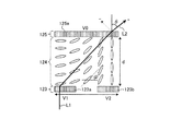
偏光素子部120は、面光源110の発光面に対向して配置された光透過性の透明基板121上に、絶縁体からなる光透過性の絶縁層122と、複数の配線パターンからなる下部電極123と、液晶分子の初期配向を一方向に揃えた液晶層124と、複数の配線パターンからなる上部電極125と、絶縁体からなる光透過性の絶縁層126と、遮光層128による凹凸を平坦化する光透過性の平坦化層127と、遮光性の素材からなる遮光層128と、光透過性の透明基板129と、をこの順に備えている。
The polarizing
なお、本実施形態では、液晶層124の駆動にかかる電極部として下部電極123及び上部電極125を備えるものとするが、電極部の態様はこれに限らず、例えば、透明基板121と絶縁層122との間、及び/又は絶縁層126と平坦化層127との間にベタ電極を備えた態様としてもよい。また、下部電極123、上部電極125のうち、何れか一方の電極をベタ電極とした態様としてもよい。
In the present embodiment, the
図3は、指向性バックライト100の電極部の一部を拡大した概略図を示している。なお、透明基板121、絶縁層122、絶縁層126及び平坦化層127の図示は省略している。
FIG. 3 shows an enlarged schematic view of a part of the electrode part of the
図3に示したように、下部電極123と上部電極125とは、ともにストライプ状の配線パターンにより構成されている。ここで、下部電極123を構成するストライプ状の配線パターンと、上部電極125を構成するストライプ状の配線パターンと、の配線方向は互いに直交するよう形成されている。なお、各配線パターンの径及び配線パターンの間隔は、特に問わないものとするが、例えば、数マイクロメートルから数10マイクロメートルのオーダーとする等微細配線とすることが好ましい。また、下部電極123及び上部電極125は、光透過性の透明電極を用いて形成することが好ましい。
As shown in FIG. 3, both the
平坦化層127(図示せず)内に保持された遮光層128には、図1、3に示したように、下部電極123及び上部電極125の配線パターンに応じた位置に開口部Aが周期的に形成されている。ここで開口部Aは、透明基板121〜平坦化層127を透過した光の照射口となり、当該開口部Aを通過した光が透明基板129を介して観測者Oから観測されることになる。
As shown in FIGS. 1 and 3, the
ここで、開口部Aは、下部電極123及び上部電極125の配線パターン間毎に形成される態様としてもよいし、当該配線パターン間のうち所定の間隔毎に形成される態様としてもよい。なお、開口部Aのサイズは、特に問わないものとするが、上述した下部電極123及び上部電極125の配線パターンの間隔に応じて形成することが好ましい。例えば、配線パターンの間隔を数マイクロメートルから数10マイクロメートルのオーダーとした場合には、このオーダーに合わせて数マイクロメートルから数10マイクロメートルのオーダーで開口部Aを形成することが好ましい。
Here, the opening A may be formed between the wiring patterns of the
下部電極123と上部電極125との間に保持された液晶層124を構成する液晶分子は、電界の影響がない初期配向において、長軸方向が一定の方向となるよう配向されている。液晶層124を構成する各液晶分子は、下部電極123及び上部電極125の各配線パターンに印加される電圧に応じて、その配向を変化させ液晶層124を透過する光線を屈折させる。以下、図4を参照して、液晶層124の屈折率変化の原理を説明する。
The liquid crystal molecules constituting the
図4は、液晶分子の初期配向に長軸方向が基板面に対して平行に並んだホモジニアス配向を用いた例を示した図である。なお、図4において、「123a」及び「123b」は、下部電極123を構成する複数の配線パターンのうち隣接する二つの配線パターンを意味している。また、「125a」は配線パターン123a、123bの上部に位置する上部電極125の配線パターンを意味している。
FIG. 4 is a diagram showing an example in which homogeneous alignment in which the major axis direction is aligned in parallel with the substrate surface is used for initial alignment of liquid crystal molecules. In FIG. 4, “123a” and “123b” mean two adjacent wiring patterns among a plurality of wiring patterns constituting the
下部電極123及び上部電極125への電圧印加により液晶層124内に電界が発生すると、図4に示したように、液晶分子の長軸方向は電界方向に応じて角度ψ傾くため、液晶層124の屈折率は変化する。この屈折率の変化により、図示しない面光源110から法線方向に照射された光線L1は、液晶層124を透過することで角度θ分偏向する。そのため、透明基板129(上部電極125)の表面上では偏向後の光線L2が観測されることになる。以下、光線L1の偏向分の角度θを偏向角度θという。
When an electric field is generated in the
上述した屈折率変化の原理から明らかなように、偏向角度θは、下部電極123及び上部電極125の各配線パターンに印加する電圧値に応じてその値は変化する。そのため、本実施形態の指向性バックライト100では、後述する制御装置130により下部電極123及び上部電極125の各配線パターンに印加する電圧値を個別的に制御することで、偏向角度θを制御する。以下、図4、5を参照して、偏向角度θの制御方法について説明する。
As is clear from the principle of refractive index change described above, the deflection angle θ changes depending on the voltage value applied to each wiring pattern of the
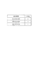
図4において、配線パターン123a、123b、125aの夫々に印加する電圧値をV1、V2、V0としている。また、電圧値V1、V2、V0の絶対値の大小関係と、当該大小関係の電圧値が印加されることで得られる光線の偏向方向(θ方向)と、の関係が図5に示したテーブルのように予め得られているものとする。ここで、「+」は図4で示した液晶層124表面の右方向、「0」は液晶層124表面の法線方向、「−」は液晶層124表面の左方向を意味している。
In FIG. 4, voltage values applied to the
この場合、後述する電圧制御部133は、図5に示したテーブルに基づいて、下部電極123の配線パターン123a、123b及び上部電極125の配線パターン125aに印加する電圧値の関係を、|V1|>|V2|=|V0|、|V0|=|V1|=|V2|、|V0|=|V1|<|V2|の3通りに切り替えることで、液晶層124を透過する光の偏向角度θを水平方向(図4中、左右方向)の3方向に制御する。
In this case, the
なお、ここでは偏向角度θを水平方向に制御する場合を説明したが、これに限らず、多の方向に制御する態様としてもよい。例えば、配線パターン125aに隣接する配線パターン(図示せず)に印加する電圧値を合わせて制御することで、図中奥行き方向(以下、垂直方向という)に光線を偏向させることができる。また、下部電極123及び上部電極125を構成する一部の配線パターン(配線パターン123a、123b、125a)についてのみ説明したが、他の配線パターンについても同様に、電圧制御部133により印加される電圧値が制御されるものとする。
Although the case where the deflection angle θ is controlled in the horizontal direction has been described here, the present invention is not limited to this and may be controlled in many directions. For example, by controlling the voltage value applied to the wiring pattern (not shown) adjacent to the
図5で示したような、下部電極123及び上部電極125の各配線パターンに印加する電圧値やその大小関係は、液晶層124の特性や遮光層128の開口部Aの大きさ等、指向性バックライト100の特性に基づいて決定される。以下、図6−1、6−2を参照して、指向性バックライト100の特性と偏向角度θとの関係について説明する。
As shown in FIG. 5, the voltage value applied to each wiring pattern of the
図6−1は、図4で示した液晶分子の配向角度(ψ)と、下部電極123及び上部電極125に印加する電圧値(V)と、の関係を示した概念図である。なお、この図では水平方向の配向角度ψを0°としている。図6−1に示したように、ホモジニアス配向の液晶分子は、電圧値の上昇に伴って配向角度ψが急激に上昇し、最大の角度90°へと近づくという特性を有している。偏向角度θは、液晶層124内の各液晶分子における配向角度ψの積重結果である。そのため、配線パターン毎に印加する電圧値を個別的に制御し配向角度ψを変位させることで、偏向角度θを任意の値とすることができる。なお、後述する電圧制御部133は、各開口部Aに対応する配線パターン単位で印加する電圧値を制御することで、各開口部Aを通過する面光源110からの光線が所定の位置(例えば、観測者Oの位置)に向かうよう制御する。
FIG. 6A is a conceptual diagram showing the relationship between the orientation angle (ψ) of the liquid crystal molecules shown in FIG. 4 and the voltage value (V) applied to the
例えば、粘性係数K=15.8×10⁻¹²N、配向方向に平行な誘電率εp=8.3・ε0、配向方向に垂直な誘電率εv=3.1・ε0、液晶層124の厚さ(液晶セルギャップ)d=5μmの液晶層124を用いた場合には、約8V以上の電圧で配向角度ψが90°となる。ここで、ε0は真空の誘電率(8,854×10-12F/m)を意味する。
For example, the viscosity coefficient K = 15.8 × 10 −12 N, the dielectric constant εp = 8.3 · ε 0 parallel to the alignment direction, the dielectric constant εv = 3.1 · ε 0 perpendicular to the alignment direction, and the
また、図6−2は、例として|V1−V2|の値が最大値のとき、屈折率差Δn=0.2、開口部Aのサイズを10μmとした場合での、偏向角度θと液晶セルギャップdとの関係を示している。この場合、液晶セルギャップが30μm以上のとき60°以上の偏向角度が得られることになる。 FIG. 6B illustrates, for example, the deflection angle θ and the liquid crystal when the value of | V1−V2 | is the maximum value, the refractive index difference Δn = 0.2, and the size of the opening A is 10 μm. The relationship with the cell gap d is shown. In this case, when the liquid crystal cell gap is 30 μm or more, a deflection angle of 60 ° or more can be obtained.
図6−1、6−2に示した液晶層124の特性や遮光層128の開口部Aのサイズ等の特性に基づいて、下部電極123及び上部電極125の各配線パターンに印加する電圧値を決定することで、任意の方向に偏向角度を制御することができる。なお、本実施形態では、水平方向及び/又は垂直方向について、互いに異なる偏向方向に光線を制御するためのN通りの電圧値(又は電圧値の大小関係)が予め導出されているものとする(Nは2以上の整数)。また、これら下部電極123及び上部電極125の各配線パターンに印加されるN通りの電圧値は、後述する記憶部132に予め記憶された設定情報1321に定義されているものとする。
Based on the characteristics of the
図7は、指向性バックライト100の駆動にかかる制御装置130を概略的に示したブロック図である。図7に示したように、制御装置130は、電力供給部131、記憶部132、電圧制御部133を備えている。
FIG. 7 is a block diagram schematically showing the
電力供給部131は、外部の商用電源等から供給される電力を、指向性バックライト100の各電力負荷部に供給する。なお、図7では、偏光素子部120にかかる電力供給線以外の図示を省略している。
The
記憶部132は、ROM等の記憶装置であって、指向性バックライト100の駆動制御にかかる各種の情報を予め記憶する。具体的には、下部電極123及び上部電極125の各配線パターンに印加する電圧値を定めた設定情報1321を予め記憶している。
The
設定情報1321には、下部電極123及び上部電極125の各配線パターンに個別的に印加するN通りの電圧値(又は電圧値の大小関係)が予め定義されている。ここで、設定情報1321に定義されたN通りの電圧値は、当該N通りの各電圧印加状態において、各開口部Aを通過する光線L2の方向が特定の位置(集光位置)に向かうよう導出された値であるものとする。また、各電圧印加状態での集光位置、即ちN個の集光位置は、互いに異なる位置が設定されているものとする。集光位置は任意の位置に設定可能であるものとするが、例えば、想定される観測者の各位置等を設定する態様としてもよい。なお、設定情報1321として記憶する情報の形態は、図5に示したようなテーブル形式としてもよいし、各配線パターンに個別的に印加するN通りの電圧値を一義的に導出可能な関係式の形態で記憶する態様としてもよい。
In the setting information 1321, N voltage values (or voltage value magnitude relationships) individually applied to the wiring patterns of the
電圧制御部133は、電力供給部131から各電力負荷部に供給される電力のうち、偏光素子部120の下部電極123及び上部電極125の各配線パターンに印加する電圧値を、記憶部132に記憶された設定情報1321に基づいて制御する。具体的に、電圧制御部133は、下部電極123及び上部電極125を構成する各配線パターンに対し、設定情報1321に定義されたN通りの電圧値を所定の時間間隔毎に切り替えながら個別的に印加する。ここで、電圧値の切り替えタイミングは、特に問わないものとするが、観測時にちらつき(フリッカー)が発生しない程度の時間間隔で行うことが好ましい。
The
このように、電圧制御部133は、N通りの電圧印加状態を所定の時間間隔毎に切り替えながら各配線パターンに与えることで、各開口部Aを通過する面光源110からの光線がN個の集光位置に向かうよう時分割制御する。これにより、指向性バックライト100から照射される光の指向性を所定の時間間隔毎に切り替えることができ、各集光位置において十分な視域を確保することができる。
Thus, the
以上のように、本実施形態によれば、単一の面光源から照射された光線の指向性を切り替えることができるため、光線の方向数を増加させることができる。また、面光源からの光線が法線方向に輝度分布が集中する特性を有することで、面光源からの光線が向かう各位置において視域を確保することができるため、視域を広げることができる。 As described above, according to the present embodiment, the directivity of light rays emitted from a single surface light source can be switched, so that the number of directions of light rays can be increased. Further, since the luminance distribution of the light from the surface light source is concentrated in the normal direction, the viewing area can be secured at each position where the light from the surface light source travels, so the viewing area can be widened. .
[第2の実施形態]
次に、第2の実施形態として、上述した指向性バックライト100を備えた画像表示装置について説明する。なお、第1の実施形態と同様の構成要素については、同一の符号を付与し、その説明を省略する。
[Second Embodiment]
Next, as a second embodiment, an image display apparatus including the above-described
図8は、第2の実施形態にかかる画像表示装置200の構造を概略的に示した水平断面図である。図8において、上方側を観測者O側、即ち、指向性バックライト100による光の照射側としている。なお、画像表示装置200は、実空間における水平面と画像表示面(発光面)とが平行になるように設置する平置き型としてもよいし、画像表示面が観測者Oに向くよう水平面から傾斜して設置する態様としてもよい。
FIG. 8 is a horizontal sectional view schematically showing the structure of the
図8に示したように、画像表示装置200は、面光源110と、当該面光源110の上部に配置された偏光素子部120と、当該偏光素子部120の上部に配置されたLCDパネル210と、から構成されている。
As shown in FIG. 8, the
LCDパネル210は、光透過性の偏光板211上に、ネマチック液晶等の液晶セル212と、光透過性の偏光板213と、をこの順に備えている。
The
偏光板211は、指向性バックライト100から入射される光線のうち、所定の方向に振動する光だけを透過する。偏光板211としては、直線偏光板、円偏光板、楕円偏光板等を用いることができる。
The
液晶セル212は、透明電極を備える一対の基板と、当該基板間に保持された液晶層を備え(何れも図示せず)、後述する同期制御部223による制御により透明電極に電圧が印加されることで、画像表示面上に画像の表示を行う液晶表示素子である。なお、液晶セル212の画像が表示される画像表示面には、実質的に水平及び垂直方向に画素がマトリクス状に配列されているものとする。この画像表示面においては、R(赤)、G(緑)、B(青)のサブ画素がアレイ状に配置されている。なお、R、G、Bのサブ画素は、カラーフィルタを画像表示面上に配置することにより実現される。
The
ここで、液晶セル212の画像表示面に配列される画素と、遮光層128の開口部Aと、の間には所定の関係が保たれている。具体的に、開口部Aのサイズは、画像表示部を正面から見た場合での、当該画像表示部の各画素を構成するサブ画素のサイズと略同等のサイズで形成されており、サブ画素のサイズよりも僅かに小さく形成されることがより好ましい。
Here, a predetermined relationship is maintained between the pixels arranged on the image display surface of the
また、下部電極123及び上部電極125の各配線パターンの径及び配線パターン間の間隔は、上述した開口部Aのサイズ、即ち、液晶セル212の画像表示面を構成するサブ画素のサイズに応じて決定されることが好ましい。この場合も、各配線パターンの径及び配線パターンの間隔は、サブ画素のサイズよりも小さく形成されることが好ましい。
Further, the diameter of each wiring pattern of the
偏光板213は、偏光板211及び液晶セル212を透過した光線のうち、所定の方向に振動する光だけを透過する。なお偏光板213は、偏光板211と同様、直線偏光板、円偏光板、楕円偏光板等を用いることができる。
The
図9は、画像表示装置200の駆動にかかる制御装置220を概略的に示したブロック図である。図9に示したとおり、制御装置220は、電力供給部221と、記憶部222と、同期制御部223と、電圧制御部224とを備えている。
FIG. 9 is a block diagram schematically showing the
電力供給部221は、外部の商用電源等から供給された電力を画像表示装置200の各電力負荷部に供給する。なお、図9では、偏光素子部120にかかる電力供給線以外の図示を省略している。
The
記憶部222は、上述した記憶部132と同様の記憶装置であって、画像表示装置200の駆動制御にかかる各種の情報を予め記憶する。具体的には、第1の実施形態と同様、下部電極123及び上部電極125の各配線パターンに印加するN通りの電圧値を定めた設定情報2221を予め記憶している。
The
設定情報2221には、上述した設定情報1321と同様、液晶層124の物理特性や遮光層128の開口部Aの大きさに基づいて定められた、下部電極123及び上部電極125を構成する各配線パターンに印加するN通りの電圧値(又は電圧値の大小関係)が予め定義されている。ここで、設定情報2221に定義されたN通りの電圧値は、当該N通りの各電圧印加状態において、各開口部Aを通過しLCDパネル210を透過する光線L2の方向が特定の集光位置に向かうよう導出された値であるものとする。また、各電圧印加状態での集光位置、即ちN個の集光位置は、互いに異なる位置が設定されているものとする。集光位置は任意の位置に設定可能であるものとするが、例えば、想定される観測者の各位置等を設定する態様としてもよい。
In the setting
同期制御部223は、記憶部222等に記憶された1フレームの画像をM個のフィールド画像に分割し(Mは2以上の整数)、これら各フィールド画像を所定の時間間隔毎に切り替えて液晶セル212の画像表示面上に表示させる。ここで、1フレームの分割数Mと、設定情報2221に定義された電圧値の組数Nと、の関係は同数又は整数倍となることが好ましい。なお、各フィールド画像の切り替えタイミングは、特に問わないものとするが、観測時にちらつき(フリッカー)が発生しない程度の時間間隔で行うことが好ましい。
The
電圧制御部224は、電力供給部221から各電力負荷部に供給される電力のうち、偏光素子部120の下部電極123及び上部電極125に印加される電圧値を、記憶部222に記憶された設定情報2221に基づいて制御する。具体的に、電圧制御部224は、下部電極123及び上部電極125を構成する各配線パターンに対し、設定情報2221に定義されたN通りの電圧値を所定の時間間隔毎に切り替えながら個別的に印加する。ここで、各配線パターンに印加する電圧の切り替えは、同期制御部223による各フィールド画像の切り替えタイミングと同期して行われるものとする。
The
このように、電圧制御部224は、N通りの電圧印加状態を所定の時間間隔毎に切り替えながら各配線パターンに与えることで、各開口部Aを通過しLCDパネル210を透過する面光源110からの光線がN個の集光位置に向かうよう時分割制御する。これにより、指向性バックライト100から照射される光の指向性を所定の時間間隔毎に切り替えることができ、各集光位置において十分な視域を確保することができる。
As described above, the
図10は、画像表示装置200を上面(観測側)から見た平面図である。同図において、F21〜23は、偏光素子部120及びLCDパネル210を透過した面光源110からの光線により確保された観測者Oa、Ob、Ocの各位置での視域を表している。
FIG. 10 is a plan view of the
なお図10では、1フレームの画像を構成する3個のフィールド画像に応じ、電圧制御部224が、各配線パターンへの印加電圧を時分割制御することで、観測者Oa、Ob、Ocの各位置に面光源110からの光線方向を制御した状態を示している。このように、画像表示面からの表示方向を水平方向(図中左右方向)に制御することで、観測者Oa、Ob、Ocの各位置に視域F21〜23を確保することで、多画面(図10では3画面)の平面表示を行うことが可能となる。
In FIG. 10, the
図11は、図10で示した画像表示装置200と各観測者Oa、Ob、Ocとの関係を示した図である。同図に示したように、電圧制御部224による電圧制御により、画像表示装置200から照射される光線の方向を、観測者Oa、Ob、Ocの位置を基準に切り替えることで、視域F21〜F23は観測者Oa、Ob、Ocの位置0を中心に確保される。なお、図中Bは、各視域F21〜F23の境界を示している。また、図中「−W」、「+W」は、各視域F21〜F23において観測者の位置0を中心とした場合での、負(−)方向及び正(+)方向の境界Bの位置を示している。
FIG. 11 is a diagram showing the relationship between the
また、図12〜図14は、図11に示した観測者Oa、Ob、Ocの各位置における視域F21〜F23と、指向性バックライト100から照射された光線L2との関係をそれぞれ示した図である。なお、指向性バックライト100の図示は省略している。
12 to 14 show the relationship between the viewing zones F21 to F23 at the positions of the observers Oa, Ob, and Oc shown in FIG. 11 and the light beam L2 emitted from the
図12〜図14に示したように、LCDパネル210上の各位置に入射する光線L2の入射角度が電圧制御部224により制御されることで、観測者O(Oa、Ob、Oc)に応じた位置に向けて光線L3が照射される。このように、光線L3の向きを観測者Oの位置に応じて切り替えることで、各観測者位置における視域F21〜F23を広く確保することができる。
As shown in FIGS. 12 to 14, the incident angle of the light beam L <b> 2 incident on each position on the
なお、図12〜図14から明らかなように、何れの場合でも画像表示部の両端部と中心部とでは観測者に向けられる光線の方向は異なっている。例えば、図14の観測者Ocの位置で画像を観測する際、画像表示面の左端から照射する光線に比べて、右端から照射する光線の照射角度の方は大きくなる。つまり、観測者Ocの位置を基準とした場合、当該観測者Ocの位置に向けて照射する光線の方向は画像表示面上の各位置で異なる。そのため、電圧制御部224は、指向性バックライト100を用いて画像表示面の各位置に対応する下部電極123及び上部電極125の各配線パターンに個別的に印加電圧を制御することで、各観測者の位置に向けて光を照射することができる。
As is clear from FIGS. 12 to 14, in any case, the direction of the light beam directed toward the observer is different between the both ends and the center of the image display unit. For example, when observing an image at the position of the observer Oc in FIG. 14, the irradiation angle of the light beam irradiated from the right end is larger than the light beam irradiated from the left end of the image display surface. That is, when the position of the observer Oc is used as a reference, the direction of the light beam emitted toward the position of the observer Oc is different at each position on the image display surface. Therefore, the
また、指向性バックライト100の遮光層128を通過する光線L2は、LCDパネル210(液晶セル212)のサブ画素単位で光線方向(偏向角度θ)を制御することができるため、液晶セル212の画像表示面に表示された画像を光線L3により精度よく表すことができ、視域F21〜F23に表される画像の画質を向上することができる。
Further, the light ray L2 passing through the
図15は、図11に対する比較例であって、従来の画像表示装置に相当する構成を示している。ここで図15は、LCDパネル210に入射する光線L2’の指向角度がない場合、即ち全て同じ方向(LCDパネル210の画像表示面の法線方向)に平行照射した場合における観測者Oa、Ob、Ocの位置での光線軌跡を示している。図15の構成は、例えば、偏光素子部120の下部電極123及び上部電極125の各配線パターンに印加する電圧値を全て一定の値とすることで実現できる。
FIG. 15 is a comparative example with respect to FIG. 11 and shows a configuration corresponding to a conventional image display apparatus. Here, FIG. 15 shows the observers Oa and Ob when there is no directivity angle of the light beam L2 ′ incident on the
図15の構成の場合、LCDパネル210を透過した光線L2’の透過光である光線L3’(画像光)は、観測者Oa、Ob、Ocの各位置において、視域F21’〜F23’を形成する。なお、図中「−W」、「+W」は、F21’〜F23’の各視域において観測者の位置0を中心とした場合での、負(−)方向及び正(+)方向の境界位置を示している。
In the case of the configuration of FIG. 15, a light beam L3 ′ (image light) that is a transmitted light beam of the light beam L2 ′ that has passed through the
ここで、視域F21’〜F23’は、同方向に平行照射された光線L2’を基に形成されるため、図11の構成と比べて各観測者位置における光量は、全体的に低下する。そのため、視域として形成される領域も図11の構成と比べて狭くなり、特に、観測者Oa、Ocの位置での視域は著しく低下している。一方、本実施形態にかかる画像表示装置200の構成では、図11に示したように、各視域F21〜F23は、ともに同程度の大きさを有しており、図15の構成と比較して広い視域を確保することが可能である。
Here, since the viewing zones F21 ′ to F23 ′ are formed on the basis of the light beam L2 ′ irradiated in parallel in the same direction, the amount of light at each observer position is generally reduced as compared with the configuration of FIG. . Therefore, the region formed as the viewing zone is also narrower than that in the configuration of FIG. 11, and the viewing zone at the positions of the observers Oa and Oc is particularly lowered. On the other hand, in the configuration of the
図16−1は、図11に示した視域F21〜F23と、図15に示した視域F21’〜F23’と、の形成にかかる偏光素子部120(下部電極123及び上部電極125)への印加電圧Vを対比した図である。また、図16−2は、図11に示した視域F21〜F23と、図15に示した視域F21’〜F23’と、の形成にかかる光線L3の照射角度、即ち、光線L2の偏向角度θを対比した図である。なお、両図とも横軸Xは、各視域での−Wから+Wの位置を意味しており、視域の中心を0としている。また、図16−2の縦軸において、偏光素子部120からの照射角度が0度で直進する場合、即ちLCDパネル210の表示面の法線方向を偏向角度θ=0°としている。
16A is a diagram of the polarizing element portion 120 (the
図16−1に示したように、視域F21〜F23の形成にかかる印加電圧Vは、各視域の−Wから+Wの位置にかけて変化させていることが分かる。また、図16−2に示したように、視域F21〜F23の形成にかかる光線L2の偏向角度θは、電圧の変化に対応し各視域の−Wから+Wの位置にかけて変化することが分かる。一方、視域F21’〜F23’については、各視域内の位置によらず印加電圧Vは一定値となるため、光線L2の偏向角度θも一定となる。 As shown in FIG. 16A, it can be seen that the applied voltage V applied to the formation of the viewing zones F21 to F23 is changed from −W to + W in each viewing zone. Also, as shown in FIG. 16B, the deflection angle θ of the light beam L2 for forming the viewing zones F21 to F23 can change from −W to + W in each viewing zone corresponding to the change in voltage. I understand. On the other hand, for the viewing zones F21 'to F23', the applied voltage V is a constant value regardless of the position in each viewing zone, so the deflection angle θ of the light beam L2 is also constant.
以上のように、本実施形態によれば、単一の面光源から照射された光線の指向性を切り替えることができるため、光線の方向数を増加させることができる。また、面光源からの光線が法線方向に輝度分布が集中する特性を有することで、面光源からの光線が向かう各位置において十分な視域を確保することができるため、視域を広げることができる。また、単一の面光源から照射された光線の指向性制御により確保された各視域に、フィールド画像をそれぞれ投影することができるため、多画面の表示を行うことが可能となる。 As described above, according to the present embodiment, the directivity of light rays emitted from a single surface light source can be switched, so that the number of directions of light rays can be increased. In addition, since the luminance distribution of the light from the surface light source is concentrated in the normal direction, a sufficient viewing zone can be secured at each position where the light from the surface light source travels, so the viewing zone is widened. Can do. In addition, since a field image can be projected onto each viewing zone secured by directivity control of light rays emitted from a single surface light source, a multi-screen display can be performed.
なお、本実施形態では、光線の指向性分布を水平3方向に制御した場合を説明したが、これに限らないものとする。 In the present embodiment, the case where the directivity distribution of light rays is controlled in three horizontal directions has been described. However, the present invention is not limited to this.
例えば、図17−1に示したように、光線の指向性分布を垂直方向に制御する態様としてもよい。この図では、平置きしたLCDパネル210の下面に、指向性バックライト100を設け、画像表示面の表示方向を水平方向(X方向)及び垂直方向(Y方向)に光線を制御した場合の概念図を示している。この場合、図10に示した水平方向への光線制御と同様に、垂直方向について観測者の視域範囲内に画像表示面から照射される光線方向、即ち面光源110から照射される光の光線方向を制御することで、垂直2方向+水平2方向、計4方向の視域F24〜F27を確保することができる。なお、各視域F24〜F27における光線の輝度分布は、面光源110の輝度分布特性から、図17−2に示したように、各視域の中央が輝度のピークとなり外縁に近づくほど低下することになる。そのため、何れの位置においても十分な視域を確保することが可能となる。
For example, as shown in FIG. 17A, the light beam directivity distribution may be controlled in the vertical direction. In this figure, a
また、本実施形態では、図11等で示した観測者Oa、Ob、Ocの各位置を、予め想定された位置として取り扱ったが、これに限らず、実測により得られる観測者の位置を用いた態様としてもよい。例えば、観測者の位置を検出する位置検出手段を別途備え、当該位置検出手段により検出された観測者の位置を集光位置として、下部電極123及び上部電極125の各配線パターンへの印加電圧が決定されるものとする。なお、この場合電圧制御部224は、位置検出手段により得られた位置に対応する電圧値を設定情報2221から導出し、当該電圧値に応じた電圧を下部電極123及び上部電極125の各配線パターンに個別的に印加することで、集光位置即ち観測者の位置に光線を集中させる。また、複数の観測者が検出された場合には、各位置に応じた観測者数に応じた電圧印加状態を、所定の時間間隔毎に切り替える態様としてもよい。
Further, in this embodiment, the positions of the observers Oa, Ob, and Oc shown in FIG. 11 and the like are handled as positions assumed in advance. However, the present invention is not limited to this, and the position of the observer obtained by actual measurement is used. It is good also as the mode which was. For example, a position detecting means for detecting the position of the observer is separately provided, and the applied voltage to each wiring pattern of the
また、LCDパネル210に表示するM個の各フィールド画像を多視点画像とし、偏向角度θの切り替え量、即ち集光位置を眼間距離に合わせれば、画像表示装置200をM眼の立体映像表示装置として用いることができる。例えば、同期制御部223の制御により、左目用と右目用との二つのフィールド画像を切り替えてLCDパネル210に表示させた場合には、2眼の立体画像表示装置とすることができる。
Further, if each of the M field images displayed on the
ここで、図18は、光線方向の切り替えを2方向とした場合における、LCDパネル210の中央部で観測される光線L3の輝度分布を示した図である。図18に示したように、制御装置220による光線方向の時分割制御により、各光線方向について輝度のピークが発生する。ここで、各輝度分布の重なり部分は、面光源110の発光特性により僅かとなっている。
Here, FIG. 18 is a diagram showing the luminance distribution of the light beam L3 observed at the center of the
上述した2眼の立体画像表示装置とする場合、図18に示したように、各集光位置におけるの輝度分布の重なりが小さいことが必要となる。そのため、2眼の立体画像表示装置として本実施形態で説明した画像表示装置200を用いることが好適である。
In the case of the above-described two-lens stereoscopic image display device, as shown in FIG. 18, it is necessary that the overlap of the luminance distributions at the respective condensing positions is small. Therefore, it is preferable to use the
[第3の実施形態]
次に、第3の実施形態として、上述した指向性バックライト100を備えた多眼方式或いは1次元IP方式の視差画像配置による立体画像表示装置について説明する。なお、第1及び第2の実施形態と同様の構成要素については、同一の符号を付与し、その説明を省略する。
[Third Embodiment]
Next, as a third embodiment, a multi-view or one-dimensional IP parallax image display device including the above-described
図19は、第3の実施形態にかかる立体画像表示装置300の構造を概略的に示した水平断面図である。図19において、上方側を観測者O側、即ち、指向性バックライト100による光の照射側としている。なお、立体画像表示装置300は、実空間における水平面と画像表示面(発光面)とが平行になるように設置する平置き型としてもよいし、画像表示面が観測者Oに向くよう水平面から傾斜して設置する態様としてもよい。
FIG. 19 is a horizontal sectional view schematically showing the structure of a stereoscopic
図19に示したように、立体画像表示装置300は、面光源110と、当該面光源110と対向する位置に配置された偏光素子部120と、当該偏光素子部120と対向する位置に配置されたLCDパネル210と、当該LCDパネル210と対向する位置に配置された視差発生素子310と、から構成されている。
As illustrated in FIG. 19, the stereoscopic
視差発生素子310は、レンチキュラー板やスリットアレイ、フライアイレンズアレイ、ピンホールアレイ等の、観測者Oの左右の目に視差を発生させるための光学素子である。
The
図20は、立体画像表示装置300の駆動にかかる制御装置320を概略的に示したブロック図である。図20に示したとおり、制御装置320は、電力供給部321と、記憶部322と、同期制御部323と、電圧制御部324とを備えている。
FIG. 20 is a block diagram schematically showing the
電力供給部321は、外部の商用電源等から供給された電力を立体画像表示装置300の各電力負荷部に供給する。なお、図20では、偏光素子部120にかかる電力供給線以外の図示を省略している。
The
記憶部322は、上述した記憶部132、222と同様の記憶装置であって、立体画像表示装置300の駆動制御にかかる各種の情報を予め記憶する。具体的には、第1、第2の実施形態と同様、下部電極123及び上部電極125の各配線パターンに印加するN通りの電圧値を定めた設定情報3221を予め記憶している。また、記憶部322は、LCDパネル210への表示対象となる後述する要素画像アレイを記憶する。
The
設定情報3221には、上述した設定情報1321、2221と同様、液晶層124の物理特性や遮光層128の開口部Aの大きさに基づいて定められた、下部電極123及び上部電極125を構成する各配線パターンに印加するN通りの電圧値(又は電圧値の大小関係)が予め定義されている。ここで、設定情報3221に定義されたN通りの電圧値は、当該N通りの各電圧印加状態において、各開口部Aを通過しLCDパネル210及び視差発生素子310を透過する光線L4の方向が特定の集光位置に向かうよう導出された値であるものとする。また、各電圧印加状態での集光位置、即ちN個の集光位置は、互いに異なる位置が設定されているものとする。集光位置は任意の位置に設定可能であるものとするが、例えば、想定される観測者の各位置等を設定する態様としてもよい。
The setting
同期制御部323は、記憶部322等に記憶された要素画像アレイをM個のフィールド画像に分割し(Mは2以上の整数)、これら各フィールド画像を所定の時間間隔毎に切り替えて液晶セル212の画像表示面上に表示させる。
The
ここで、要素画像アレイとは、立体画像の元となる画像を構成する要素となる複数の要素画像から構成される一フレーム分の画像である。なお、要素画像には、複数の視点から立体表示の対象となる対象物を撮影することで得られた当該視点数に応じた数の視点画像が含まれているものとする。これら要素画像は、視差発生素子310を介して観測されると、当該視差発生素子310による両目視差の発生により、各要素画像に含まれた同視点位置の視点画像が選択的に見えることになる。これにより、観測者から見て、要素画像の集まりは所定の位置に結像した立体画像として認識される。
Here, the element image array is an image for one frame composed of a plurality of element images which are elements constituting an image that is a source of a stereoscopic image. It is assumed that the element image includes a number of viewpoint images corresponding to the number of viewpoints obtained by photographing an object to be stereoscopically displayed from a plurality of viewpoints. When these element images are observed through the
なお、1フレームの分割数Mと、設定情報3221に定義された電圧値の組数Nと、の関係は同数又は整数倍となることが好ましい。また、各フィールド画像の切り替えタイミングは、特に問わないものとするが、観測時にちらつき(フリッカー)が発生しない程度の時間間隔で行うことが好ましい。
The relationship between the number of divisions M per frame and the number N of voltage value groups defined in the setting
電圧制御部324は、電力供給部321から各電力負荷部に供給される電力のうち、偏光素子部120の下部電極123及び上部電極125に印加される電圧値を、記憶部322に記憶された設定情報3221に基づいて制御する。具体的に、電圧制御部324は、下部電極123及び上部電極125を構成する各配線パターンに対し、設定情報3221に定義されたN通りの電圧値を所定の時間間隔毎に切り替えながら個別的に印加する。ここで、各配線パターンに印加する電圧の切り替えは、同期制御部323による各フィールド画像の切り替えタイミングと同期して行われるものとする。
The
このように、電圧制御部324は、N通りの電圧印加状態を所定の時間間隔毎に切り替えながら各配線パターンに与えることで、各開口部Aを通過しLCDパネル210を透過する面光源110からの光線がN個の集光位置に向かうよう時分割制御する。これにより、指向性バックライト100から照射される光の指向性を所定の時間間隔毎に切り替えることができ、各集光位置において十分な視域を確保することができる。
As described above, the
図21は、視差発生素子310にレンチキュラー板311を用いた場合を示した図である。なお、図21では、立体画像表示装置300の右端、中央、左端のみを抜粋して示している(図22〜24、26、28〜30も同様)。
FIG. 21 is a diagram showing a case where a
また、図22〜24は、図21に示した構成に対応する図であって、各フィールド画像の表示時における光線方向の遷移を示した概念図である。なお、指向性バックライト100自体の図示は省略している。また、図25は、図21の構成での画像表示面の中央付近を透過する光線の軌跡を示した図である。
FIGS. 22 to 24 are diagrams corresponding to the configuration shown in FIG. 21, and are conceptual diagrams showing the transition of the light beam direction when each field image is displayed. Illustration of the
図21に示したように、LCDパネル210の画像表示面と対向する位置に視差発生素子310としてのレンチキュラー板311が配置されている。ここで、LCDパネル210とレンチキュラー板311とは、LCDパネル210からの光線L3(画像光)がレンチキュラー板311を介して投影されるよう、レンズ焦点面外の像面の位置に画素面が配置されている。なお、レンチキュラー板311を構成する各レンズの径は、液晶セル212を構成するサブ画素の整数倍の大きさを有している。
As shown in FIG. 21, a
図21では、1フレーム分の要素画像アレイを3つのフィールド画像に分割した例を示している。同図において、幅Peは、レンチキュラー板311を構成する一のレンズに割り当てられた要素画像分の画像長を示している。また、レンチキュラー板311を構成する各レンズには、要素画像e1、e2、e3のうち何れかの画像が投影され、この投影された画像光を観測可能な視域F31がレンチキュラー板311の各レンズを透過する光線L4により確保されるようになっている。なお、図21において、L2は指向性バックライト100から照射された光線を意味している。
FIG. 21 shows an example in which an element image array for one frame is divided into three field images. In the figure, the width Pe indicates the image length of the element image assigned to one lens constituting the
具体的に、電圧制御部324は、幅Pe分の要素画像e1、e2、e3単位で、指向性バックライト100からの光線L2の入射角度(偏光素子部120での偏向角度θ)をN通りに制御する。つまり、電圧制御部324は、図22〜24に示したように、下部電極123及び上部電極125の各配線パターンに印加する電圧値を所定の時間間隔毎にN通りに切り替えながら個別的に制御することで、各フィールド画像の表示タイミングに応じて、光線L4の集光位置を切り替える。
Specifically, the
図26は、視差発生素子310の中央部で観測される光線の輝度分布を示した図である。なお、図26では、光線方向の切り替えを3方向とし、各方向にそれぞれ3視差分の表示を行った計9視差を時分割表示した場合での輝度分布を示している。
FIG. 26 is a diagram showing the luminance distribution of light rays observed at the central portion of the
図26に示したように、制御装置320による光線方向の時分割制御により、各光線方向について輝度のピークが発生する。ここで、各輝度分布の重なり部分は、面光源110の発光特性により僅かとなっている。なお、立体画像の表示を行う立体画像表示装置300では視差間のクロストークが大きいため、輝度分布の重なりがある程度あっても表示される立体画像には影響は生じない。
As shown in FIG. 26, the time peak control of the light beam direction by the
ところで、上述した幅Peは、立体画像表示装置300の特性に応じて決定される。例えば、光線方向の切り替えを行わない従来の構成(図27参照)における幅Peは、レンチキュラー板311と集光位置との間の距離、レンチキュラー板311のレンズピッチ、LCDパネル210とレンチキュラー板311との間の距離に基づき、各集光位置を含む視距離面上の視点からアパーチャ中心を液晶セル212上に投影した間隔により決定される。
By the way, the width Pe described above is determined according to the characteristics of the stereoscopic
一方、本実施形態の立体画像表示装置300における幅Peは、時分割により光線方向をN通りに切り替えるため、上述した従来の構成の幅Peと比較し、図21のように幅PeをN倍とすることができる。これにより、レンチキュラー板311の各レンズを透過する光線L4により確保される視域F31を、光線方向の切り替えを行わない従来の構成と比較しN倍に拡大させることができる。なお、図21では、光線方向を互いに異なる3通りの方向に切り替えた場合を例示しており、切り替え数に応じた3つ分の要素画像長が幅Peとなっている。
On the other hand, the width Pe in the stereoscopic
また、立体画像表示装置300の構成では、レンチキュラー板311を構成するレンズのレンズピッチに対し幅PeはN倍となるため、レンチキュラー板311のレンズピッチを1/Nとすることで、当該レンチキュラー板311を介して観測される画像光の解像度をN倍とすることができる。即ち、図21の構成では、レンチキュラー板311のレンズピッチを1/3とすることで、当該レンチキュラー板311を介して観測される画像光の解像度を3倍とすることができる。
Further, in the configuration of the stereoscopic
また、レンチキュラー板311とLCDパネル210との間隔を大きくするに伴い、視域F31は狭くなるが、液晶セル212の画素ピッチが同一である限り、各要素画像に対応するレンズを通して射出される光線L4の光線密度は大きくなるため、表示される立体画像の飛び出し・奥行き再現範囲をN倍とすることができる。即ち、図21の構成では、立体画像の飛び出し・奥行き再現範囲を3倍とすることができる。
Further, as the distance between the
一方、図27、28は、図21、25の構成に対する比較例を示した図であって、光線方向の時分割制御を行わない指向性バックライト100’を備えた、従来の立体画像表示装置に相当する構成を示している。ここで図27は、LCDパネル210に入射する光線L2’の指向角度がない場合、即ち全て同じ方向に平行照射した場合での光線軌跡を示している。また、図28は、図27の構成における画像表示部の中央付近の光線軌跡を示した図である。なお、光線L3’は、LCDパネル210とレンチキュラー板311との間の光線を意味している。
On the other hand, FIGS. 27 and 28 are diagrams showing a comparative example with respect to the configurations of FIGS. 21 and 25, and a conventional stereoscopic image display device including a
光線方向の時分割制御を行わない従来の構成の場合、レンチキュラー板311の各レンズに割り当てられる幅Peは、上述したように、図21の幅Peの1/3としかならない。そのため、図28に示したように、レンチキュラー板311を透過する光線L4’の光線密度は、図25に示した光線L4の光線密度と比較し、切り替え数に応じた分だけ低下する。
In the case of a conventional configuration that does not perform time-division control in the light beam direction, the width Pe assigned to each lens of the
以上のように、本実施形態によれば、単一の面光源から照射された光線の指向性を切り替えることができるため、光線の方向数を増加させることができる。また、面光源からの光線が法線方向に輝度分布が集中する特性を有することで、面光源からの光線が向かう各位置において十分な視域を確保することができるため、視域を広げることができる。また、本実施形態の立体画像表示装置300の構成では、光線方向の時分割制御を行わない従来の構成と比較し、立体表示における視域、解像度、飛び出し量の何れか一つを切り替え数Nに応じた値に向上させることが可能となる。
As described above, according to the present embodiment, the directivity of light rays emitted from a single surface light source can be switched, so that the number of directions of light rays can be increased. In addition, since the luminance distribution of the light from the surface light source is concentrated in the normal direction, a sufficient viewing zone can be secured at each position where the light from the surface light source travels, so the viewing zone is widened. Can do. In addition, in the configuration of the stereoscopic
なお、本実施形態では、視差発生素子310としてレンチキュラー板311を用いた構成を説明したが、これに限らず、他の光学素子により観測者Oの視差を発生させる態様としてもよい。
In the present embodiment, the configuration using the
例えば、図29に示したように、視差発生素子310としてフライアイレンズ312を用いる態様としてもよい。なお、フライアイレンズ312を構成する各レンズの径は、液晶セル212の画像表示面を構成するサブ画素の大きさの整数倍となるよう形成されているものとする。
For example, as shown in FIG. 29, a fly-
図29の構成の場合、下部電極123及び上部電極125の各配線パターンに印加する電圧値を個別的に制御し、水平方向及び垂直方向に光線を偏向させることで垂直方向の視差を得ることができる。ただし、水平方向及び垂直方向に光線方向を時分割制御するためには、分割数Nが大きくなるため偏光板211、液晶セル212及び偏光板213とも高速応答性を持つ必要がある。
In the case of the configuration of FIG. 29, it is possible to obtain vertical parallax by individually controlling the voltage value applied to each wiring pattern of the
また、光量は低下することになるが、図30、31に示したように、視差発生素子310としてスリットアレイ313やピンホールアレイ314を用いる態様としてもよい。なお、スリットアレイ313を構成する各スリットの間隔は、液晶セル212の画像表示面を構成するサブ画素の大きさの整数倍となるよう形成されているものとする。また、ピンホールアレイを構成する各ピンホールの径は、液晶セル212の画像表示面を構成するサブ画素の大きさの整数倍となるよう形成されているものとする。
Although the amount of light is reduced, as shown in FIGS. 30 and 31, a
以上、発明の実施の形態について説明したが、本発明はこれに限定されるものではなく、本発明の主旨を逸脱しない範囲での種々の変更、置換、追加などが可能である。 Although the embodiments of the invention have been described above, the present invention is not limited to these embodiments, and various modifications, substitutions, additions, and the like can be made without departing from the spirit of the present invention.
100 指向性バックライト
110 面光源
120 偏光素子部
121 透明基板
122 絶縁層
123 下部電極
124 液晶層
125 上部電極
126 絶縁層
127 平坦化層
128 遮光層
129 透明基板
130 制御装置
131 電力供給部
132 記憶部
1321 設定情報
133 電圧制御部
200 画像表示装置
210 LCDパネル
211 偏光板
212 液晶セル
213 偏光板
220 制御装置
221 電力供給部
222 記憶部
2221 設定情報
223 同期制御部
224 電圧制御部
300 立体画像表示装置
310 視差発生素子
311 レンチキュラー板
312 フライアイレンズ
313 スリットアレイ
314 ピンホールアレイ
320 制御装置
321 電力供給部
322 記憶部
3221 設定情報
323 同期制御部
324 電圧制御部
DESCRIPTION OF
Claims (16)
前記面光源の発光面に対向して配置された第1の透明基板と、前記第1の透明基板と対向して配置された第2の透明基板と、前記第1及び第2の透明基板間に形成され一方又は両方がストライプ状の配線パターンを有した、対向する一対の電極から構成される複数の電極対と、前記電極間に保持された液晶層と、前記第2の透明基板上に配置され前記電極対の配線パターンに応じた開口部を有する遮光層と、を備えた偏向素子部と、
前記電極の各配線パターンへの電圧印加状態を複数通りに切り替え、各電圧印加状態において、前記電極対毎に当該電極対を構成する電極に印加する電圧値を個別的に制御することで、前記各開口部を通過する前記面光源からの光線が所定の位置に向かうよう制御する電圧制御手段と、
を備えたことを特徴とする指向性バックライト。 A surface light source having a characteristic that the luminance distribution is concentrated in the normal direction of the light emitting surface;
A first transparent substrate disposed to face the light emitting surface of the surface light source, a second transparent substrate disposed to face the first transparent substrate, and between the first and second transparent substrates A plurality of electrode pairs formed of a pair of opposing electrodes, one or both of which has a stripe-like wiring pattern, a liquid crystal layer held between the electrodes, and the second transparent substrate A light-shielding layer having an opening corresponding to the wiring pattern of the electrode pair disposed, and a deflection element unit,
By switching the voltage application state to each wiring pattern of the electrode in a plurality of ways, and individually controlling the voltage value applied to the electrode constituting the electrode pair for each electrode pair in each voltage application state, Voltage control means for controlling the light from the surface light source passing through each opening to go to a predetermined position;
A directional backlight characterized by comprising
前記面光源の発光面に対向して配置された第1の透明基板と、前記第1の透明基板と対向して配置された第2の透明基板と、前記第1及び第2の透明基板間に形成され一方又は両方がストライプ状の配線パターンを有した一対の電極と、前記電極間に保持された液晶層と、前記第2の透明基板上に配置され前記電極の配線パターンに応じた複数の開口部を有する遮光層と、を備えた偏向素子部と、
前記偏向素子部と対向して配置され、マトリクス状に配置された表示画素に複数個のフィールド画像に分割された1フレーム分の画像を表示する液晶表示素子と、
前記液晶表示素子に表示された各フィールド画像を所定の時間間隔毎に切り替える同期制御手段と、
前記電極の各配線パターンへの電圧印加状態を前記同期制御手段の切り替えタイミングに応じて複数通りに切り替え、各電圧印加状態において、前記各配線パターンに印加する電圧値を個別的に制御することで、前記各開口部を通過し前記液晶表示素子を透過する前記面光源からの光線が所定の位置に向かうよう制御する電圧制御手段と、
を備えたことを特徴とする表示装置。 A surface light source having a characteristic that the luminance distribution is concentrated in the normal direction of the light emitting surface;
A first transparent substrate disposed to face the light emitting surface of the surface light source, a second transparent substrate disposed to face the first transparent substrate, and between the first and second transparent substrates A pair of electrodes, one or both of which has a striped wiring pattern, a liquid crystal layer held between the electrodes, and a plurality of electrodes arranged on the second transparent substrate according to the wiring pattern of the electrodes A light shielding layer having an opening of
A liquid crystal display element arranged opposite to the deflection element unit and displaying an image for one frame divided into a plurality of field images on display pixels arranged in a matrix;
Synchronization control means for switching each field image displayed on the liquid crystal display element at predetermined time intervals;
By switching the voltage application state to each wiring pattern of the electrode in a plurality of ways according to the switching timing of the synchronization control means, and individually controlling the voltage value applied to each wiring pattern in each voltage application state Voltage control means for controlling a light beam from the surface light source that passes through each of the openings and passes through the liquid crystal display element to go to a predetermined position;
A display device comprising:
前記電圧制御手段は、前記同期制御手段の切り替えタイミングと同期して前記電圧印加状態を2通りに切り替えることを特徴とする請求項4〜7の何れか一項に記載の表示装置。 The synchronization control means switches the field image for the left eye and the field image for the right eye displayed on the liquid crystal display element at predetermined time intervals,
The display device according to claim 4, wherein the voltage control unit switches the voltage application state in two ways in synchronization with a switching timing of the synchronization control unit.
前記面光源の発光面に対向して配置された第1の透明基板と、前記第1の透明基板と対向して配置された第2の透明基板と、前記第1及び第2の透明基板間に形成され一方又は両方がストライプ状の配線パターンを有した一対の電極と、前記電極間に保持された液晶層と、前記第2の透明基板上に配置され前記電極の配線パターンに応じた複数の開口部を有する遮光層と、を備えた偏向素子部と、
前記偏向素子部と対向して配置され、マトリクス状に配置された表示画素に複数個のフィールド画像からなる立体表示のための要素画像アレイを表示する液晶表示素子と、
前記液晶表示素子の前面又は背面に配置された視差発生手段と、
前記電極の各配線パターンへの電圧印加状態を、前記各フィールド画像の表示に応じて、複数通りに切り替え、各電圧印加状態において、前記各配線パターンに印加する電圧値を個別的に制御することで、前記開口部を通過し前記液晶表示素子及び視差発生手段を透過する前記面光源からの光線が所定の位置に向かうよう制御する電圧制御手段と、
を備えたことを特徴とする立体画像表示装置。 A surface light source having a characteristic that the luminance distribution is concentrated in the normal direction of the light emitting surface;
A first transparent substrate disposed to face the light emitting surface of the surface light source, a second transparent substrate disposed to face the first transparent substrate, and between the first and second transparent substrates A pair of electrodes, one or both of which has a striped wiring pattern, a liquid crystal layer held between the electrodes, and a plurality of electrodes arranged on the second transparent substrate according to the wiring pattern of the electrodes A light shielding layer having an opening of
A liquid crystal display element that is arranged to face the deflection element unit and displays an element image array for stereoscopic display composed of a plurality of field images on display pixels arranged in a matrix;
Parallax generating means disposed on the front surface or the back surface of the liquid crystal display element;
The voltage application state to each wiring pattern of the electrode is switched in plural ways according to the display of each field image, and the voltage value applied to each wiring pattern is individually controlled in each voltage application state. And a voltage control means for controlling a light beam from the surface light source that passes through the opening and passes through the liquid crystal display element and the parallax generating means to go to a predetermined position;
A stereoscopic image display device comprising:
前記レンチキュラー板を構成する各レンズの幅が、前記表示画素を構成するサブ画素の大きさの整数倍であることを特徴とする請求項10に記載の立体画像表示装置。 The parallax generating means is a lenticular plate,
The stereoscopic image display device according to claim 10, wherein the width of each lens constituting the lenticular plate is an integral multiple of the size of a sub-pixel constituting the display pixel.
前記スリットアレイを構成する各スリットの間隔が、前記液晶表示素子を構成するサブ画素の大きさの整数倍であることを特徴とする請求項10に記載の立体画像表示装置。 The parallax generating means is a slit array,
The stereoscopic image display device according to claim 10, wherein an interval between the slits constituting the slit array is an integral multiple of a size of a sub-pixel constituting the liquid crystal display element.
前記フライアイレンズを構成する各レンズの径が、前記液晶表示素子を構成するサブ画素の大きさの整数倍であることを特徴とする請求項10に記載の立体画像表示装置。 The parallax generating means is a fly-eye lens,
The stereoscopic image display device according to claim 10, wherein a diameter of each lens constituting the fly-eye lens is an integral multiple of a size of a sub-pixel constituting the liquid crystal display element.
前記ピンホールアレイを構成する各ピンホールの径が、前記液晶表示素子を構成するサブ画素の大きさの整数倍であることを特徴とする請求項10に記載の立体画像表示装置。 The parallax generating means is a pinhole array,
The stereoscopic image display device according to claim 10, wherein a diameter of each pinhole constituting the pinhole array is an integral multiple of a size of a sub-pixel constituting the liquid crystal display element.
Priority Applications (4)
| Application Number | Priority Date | Filing Date | Title |
|---|---|---|---|
| JP2007218499A JP5248062B2 (en) | 2007-08-24 | 2007-08-24 | Directional backlight, display device, and stereoscopic image display device |
| US12/195,683 US7954967B2 (en) | 2007-08-24 | 2008-08-21 | Directional backlight, display apparatus, and stereoscopic display apparatus |
| CNA2008102100066A CN101373054A (en) | 2007-08-24 | 2008-08-22 | Directional backlight, display device and stereoscopic display device |
| US13/067,045 US20110211142A1 (en) | 2007-08-24 | 2011-05-04 | Directional backlight, display apparatus, and stereoscopic display apparatus |
Applications Claiming Priority (1)
| Application Number | Priority Date | Filing Date | Title |
|---|---|---|---|
| JP2007218499A JP5248062B2 (en) | 2007-08-24 | 2007-08-24 | Directional backlight, display device, and stereoscopic image display device |
Related Child Applications (1)
| Application Number | Title | Priority Date | Filing Date |
|---|---|---|---|
| JP2012108819A Division JP2012181544A (en) | 2012-05-10 | 2012-05-10 | Stereoscopic image display device and control device |
Publications (2)
| Publication Number | Publication Date |
|---|---|
| JP2009053345A JP2009053345A (en) | 2009-03-12 |
| JP5248062B2 true JP5248062B2 (en) | 2013-07-31 |
Family
ID=40381951
Family Applications (1)
| Application Number | Title | Priority Date | Filing Date |
|---|---|---|---|
| JP2007218499A Expired - Fee Related JP5248062B2 (en) | 2007-08-24 | 2007-08-24 | Directional backlight, display device, and stereoscopic image display device |
Country Status (3)
| Country | Link |
|---|---|
| US (2) | US7954967B2 (en) |
| JP (1) | JP5248062B2 (en) |
| CN (1) | CN101373054A (en) |
Families Citing this family (73)
| Publication number | Priority date | Publication date | Assignee | Title |
|---|---|---|---|---|
| TWI409778B (en) * | 2008-12-25 | 2013-09-21 | Innolux Corp | Liquid crystal display apparatus, liquid crystal display panel and driving method |
| US7978407B1 (en) | 2009-06-27 | 2011-07-12 | Holovisions LLC | Holovision (TM) 3D imaging with rotating light-emitting members |
| KR101068880B1 (en) * | 2009-12-16 | 2011-09-30 | 주식회사 파버나인코리아 | Multi-mode Stereoscopic Display |
| US8964013B2 (en) | 2009-12-31 | 2015-02-24 | Broadcom Corporation | Display with elastic light manipulator |
| US8823782B2 (en) * | 2009-12-31 | 2014-09-02 | Broadcom Corporation | Remote control with integrated position, viewer identification and optical and audio test |
| US9247286B2 (en) * | 2009-12-31 | 2016-01-26 | Broadcom Corporation | Frame formatting supporting mixed two and three dimensional video data communication |
| US8854531B2 (en) | 2009-12-31 | 2014-10-07 | Broadcom Corporation | Multiple remote controllers that each simultaneously controls a different visual presentation of a 2D/3D display |
| CN102156358B (en) * | 2010-02-12 | 2016-04-20 | 群创光电股份有限公司 | Liquid crystal display device, liquid crystal display panel, and driving method |
| US8587498B2 (en) * | 2010-03-01 | 2013-11-19 | Holovisions LLC | 3D image display with binocular disparity and motion parallax |
| CN102213838A (en) * | 2010-04-06 | 2011-10-12 | 宇威光电股份有限公司 | Stereoscopic display device |
| KR101725044B1 (en) * | 2010-05-27 | 2017-04-11 | 삼성전자주식회사 | Imaging display apparatus |
| JP2011258740A (en) * | 2010-06-09 | 2011-12-22 | Toshiba Corp | Semiconductor device, camera module, and manufacturing method of semiconductor device |
| US9052565B2 (en) | 2010-11-17 | 2015-06-09 | Panasonic Intellectual Property Management Co., Ltd. | Light deflector and liquid crystal display device using the same |
| JP2012123325A (en) * | 2010-12-10 | 2012-06-28 | Toshiba Corp | Stereoscopic image display device |
| JP5050094B2 (en) * | 2010-12-21 | 2012-10-17 | 株式会社東芝 | Video processing apparatus and video processing method |
| CN102141714B (en) * | 2011-03-31 | 2013-10-23 | 昆山龙腾光电有限公司 | Display device |
| WO2012153499A1 (en) * | 2011-05-10 | 2012-11-15 | パナソニック株式会社 | Display device, display method, integrated circuit, program |
| CN102314016A (en) * | 2011-08-10 | 2012-01-11 | 南京中电熊猫液晶显示科技有限公司 | Liquid crystal display panel capable of enhancing three-dimensional (3D) display effect and manufacturing method thereof |
| US8672499B2 (en) * | 2011-11-18 | 2014-03-18 | Shenzhen China Star Optoelectronics Technology Co., Ltd. | Flat panel display device, stereoscopic display device, plasma display device |
| US9979950B2 (en) * | 2011-12-21 | 2018-05-22 | Sharp Kabushiki Kaisha | Imaging device and electronic information instrument |
| US8985785B2 (en) | 2012-01-25 | 2015-03-24 | International Business Machines Corporation | Three dimensional laser image projector |
| US9004700B2 (en) | 2012-01-25 | 2015-04-14 | International Business Machines Corporation | Three dimensional image projector stabilization circuit |
| US9325977B2 (en) * | 2012-01-25 | 2016-04-26 | International Business Machines Corporation | Three dimensional LCD monitor display |
| US8960913B2 (en) | 2012-01-25 | 2015-02-24 | International Busniess Machines Corporation | Three dimensional image projector with two color imaging |
| US9104048B2 (en) | 2012-01-25 | 2015-08-11 | International Business Machines Corporation | Three dimensional image projector with single modulator |
| US8992024B2 (en) | 2012-01-25 | 2015-03-31 | International Business Machines Corporation | Three dimensional image projector with circular light polarization |
| US20130188149A1 (en) | 2012-01-25 | 2013-07-25 | International Business Machines Corporation | Three dimensional image projector |
| KR101320052B1 (en) * | 2012-01-31 | 2013-10-21 | 한국과학기술연구원 | 3-dimensional display apparatus using extension of viewing zone width |
| JP5893447B2 (en) | 2012-03-08 | 2016-03-23 | 株式会社ジャパンディスプレイ | Liquid crystal lens, display device, and electronic device |
| WO2013161304A1 (en) * | 2012-04-26 | 2013-10-31 | パナソニック株式会社 | Optical deflection element and image display device using this |
| US9188731B2 (en) | 2012-05-18 | 2015-11-17 | Reald Inc. | Directional backlight |
| TWI636283B (en) | 2012-05-18 | 2018-09-21 | 美商瑞爾D斯帕克有限責任公司 | Directional backlight, directional display device and control method thereof |
| CN104380185B (en) | 2012-05-18 | 2017-07-28 | 瑞尔D斯帕克有限责任公司 | Directional backlight |
| JP6096466B2 (en) * | 2012-10-23 | 2017-03-15 | 株式会社東芝 | Imaging device |
| CN103207457B (en) * | 2012-12-05 | 2014-10-22 | 深圳市亿思达显示科技有限公司 | Three-dimensional display device |
| JP6584008B2 (en) | 2013-02-22 | 2019-10-02 | リアルディー スパーク エルエルシー | Directional backlight |
| KR102014982B1 (en) * | 2013-03-15 | 2019-08-27 | 삼성전자주식회사 | Display apparatus for visul/audio multiplexed display |
| CN104297929B (en) * | 2013-07-19 | 2017-02-08 | 华为技术有限公司 | Stereoscopic imaging device, method and display |
| KR102366346B1 (en) | 2013-10-14 | 2022-02-23 | 리얼디 스파크, 엘엘씨 | Light input for directional backlight |
| KR102134904B1 (en) | 2013-10-30 | 2020-07-17 | 삼성디스플레이 주식회사 | Three dimensional image display and liquid crystal lens therefor |
| KR20150086696A (en) | 2014-01-20 | 2015-07-29 | 한국전자통신연구원 | directional back lighting unit |
| EP3204686B1 (en) * | 2014-10-08 | 2019-07-17 | RealD Spark, LLC | Connection unit for a directional backlight |
| KR20160067546A (en) | 2014-12-04 | 2016-06-14 | 한국전자통신연구원 | Directional back light unit |
| KR102251896B1 (en) * | 2014-12-31 | 2021-05-13 | 엘지디스플레이 주식회사 | Hologram display apparatus and a method for controling the same |
| RU2596062C1 (en) | 2015-03-20 | 2016-08-27 | Автономная Некоммерческая Образовательная Организация Высшего Профессионального Образования "Сколковский Институт Науки И Технологий" | Method for correction of eye image using machine learning and method of machine learning |
| WO2016168345A1 (en) | 2015-04-13 | 2016-10-20 | Reald Inc. | Wide angle imaging directional backlights |
| KR102598709B1 (en) | 2015-09-02 | 2023-11-06 | 삼성전자주식회사 | Backlight unit using micro optical switch, and display apparatus having the same |
| KR102421062B1 (en) * | 2015-11-20 | 2022-07-14 | 에스엘 주식회사 | Automotive lamp |
| CN114143495B (en) | 2016-01-05 | 2025-07-15 | 瑞尔D斯帕克有限责任公司 | Gaze Correction for Multi-View Images |
| US11079619B2 (en) | 2016-05-19 | 2021-08-03 | Reald Spark, Llc | Wide angle imaging directional backlights |
| CN109496258A (en) | 2016-05-23 | 2019-03-19 | 瑞尔D斯帕克有限责任公司 | Wide-angle image directional backlight |
| KR101826025B1 (en) * | 2016-07-22 | 2018-02-07 | 한국과학기술연구원 | System and method for generating 3d image contents that user interaction is possible |
| KR20180036821A (en) * | 2016-09-30 | 2018-04-10 | 삼성디스플레이 주식회사 | Stereoscopic image display device |
| CN108253338A (en) * | 2016-12-27 | 2018-07-06 | 天津三星电子有限公司 | Light-emitting device, its transmitting angular method of adjustment and device |
| US10401638B2 (en) | 2017-01-04 | 2019-09-03 | Reald Spark, Llc | Optical stack for imaging directional backlights |
| WO2018187154A1 (en) | 2017-04-03 | 2018-10-11 | Reald Spark, Llc | Segmented imaging directional backlights |
| EP4293574A3 (en) | 2017-08-08 | 2024-04-03 | RealD Spark, LLC | Adjusting a digital representation of a head region |
| EP3707554B1 (en) | 2017-11-06 | 2023-09-13 | RealD Spark, LLC | Privacy display apparatus |
| CN118672006A (en) | 2018-01-25 | 2024-09-20 | 瑞尔D斯帕克有限责任公司 | Touch screen for privacy display |
| CN108513125B (en) * | 2018-06-09 | 2023-08-25 | 成都工业学院 | Integrated imaging 3D display device based on barrier |
| CN114335382B (en) * | 2018-12-07 | 2025-03-28 | 京东方科技集团股份有限公司 | Display module and preparation method thereof |
| JP6919673B2 (en) | 2019-05-07 | 2021-08-18 | オムロン株式会社 | Display switching device |
| CN114144719A (en) * | 2019-08-02 | 2022-03-04 | 松下知识产权经营株式会社 | Display device |
| CN111123540B (en) * | 2020-03-01 | 2025-01-07 | 成都工业学院 | A variable depth stereoscopic display device based on double aperture |
| JP7516781B2 (en) * | 2020-03-04 | 2024-07-17 | 富士フイルムビジネスイノベーション株式会社 | Display system, display control device and program |
| CN111781736B (en) * | 2020-08-30 | 2023-07-14 | 成都航空职业技术学院 | 3D display device and method based on composite pinhole polarizer |
| EP4214441A4 (en) | 2020-09-16 | 2024-08-28 | RealD Spark, LLC | VEHICLE EXTERIOR LIGHTING DEVICE |
| JP7558783B2 (en) * | 2020-12-10 | 2024-10-01 | 株式会社ジャパンディスプレイ | Liquid Crystal Devices |
| CN113703178B (en) * | 2021-09-11 | 2023-05-30 | 成都航空职业技术学院 | Integrated imaging 3D display device with uniform resolution |
| US11966049B2 (en) | 2022-08-02 | 2024-04-23 | Reald Spark, Llc | Pupil tracking near-eye display |
| WO2024035796A1 (en) | 2022-08-11 | 2024-02-15 | Reald Spark, Llc | Anamorphic directional illumination device |
| JP2024058952A (en) * | 2022-10-17 | 2024-04-30 | オムロン株式会社 | Display switching device, vehicle display system, and automobile |
| CN117518519B (en) * | 2023-12-29 | 2024-03-05 | 成都工业学院 | A three-dimensional display device with arc-shaped viewpoint arrangement |
Family Cites Families (13)
| Publication number | Priority date | Publication date | Assignee | Title |
|---|---|---|---|---|
| JP2983891B2 (en) * | 1995-05-30 | 1999-11-29 | 三洋電機株式会社 | 3D display device |
| JPH0980354A (en) * | 1995-09-12 | 1997-03-28 | Toshiba Corp | Stereoscopic imager |
| JP3710934B2 (en) | 1998-04-21 | 2005-10-26 | 三洋電機株式会社 | 3D image display device without glasses |
| US20020001045A1 (en) * | 1998-07-16 | 2002-01-03 | Minakanagurki Ranganath | Parallax viewing system |
| JP3585781B2 (en) | 1999-08-31 | 2004-11-04 | 株式会社東芝 | 3D display device |
| JP2004212648A (en) * | 2002-12-27 | 2004-07-29 | Olympus Corp | Video display device and video display method |
| JP2005077437A (en) * | 2003-08-29 | 2005-03-24 | Olympus Corp | Video display device, stereoscopic video display device, and on-vehicle video display device |
| CN100459719C (en) * | 2003-09-04 | 2009-02-04 | 株式会社东芝 | Three-dimensional image display device and method, and image data generation method for three-dimensional display |
| US7480022B2 (en) * | 2003-12-10 | 2009-01-20 | Seiko Epson Corporation | Liquid crystal display device, method of manufacturing liquid crystal display device, and electronic apparatus |
| JP4285350B2 (en) * | 2004-02-26 | 2009-06-24 | セイコーエプソン株式会社 | Viewing angle control element and manufacturing method thereof, liquid crystal display device, electronic device |
| JP2006208605A (en) * | 2005-01-26 | 2006-08-10 | Asahi Glass Co Ltd | Display device and directivity control element |
| JP4331134B2 (en) * | 2005-03-25 | 2009-09-16 | 株式会社東芝 | Stereoscopic image display device |
| KR101201848B1 (en) * | 2006-02-20 | 2012-11-15 | 삼성디스플레이 주식회사 | Stereo-scopic image conversion panel and stereo-scopic image display apparatus having the same |
-
2007
- 2007-08-24 JP JP2007218499A patent/JP5248062B2/en not_active Expired - Fee Related
-
2008
- 2008-08-21 US US12/195,683 patent/US7954967B2/en not_active Expired - Fee Related
- 2008-08-22 CN CNA2008102100066A patent/CN101373054A/en active Pending
-
2011
- 2011-05-04 US US13/067,045 patent/US20110211142A1/en not_active Abandoned
Also Published As
| Publication number | Publication date |
|---|---|
| US7954967B2 (en) | 2011-06-07 |
| US20090052164A1 (en) | 2009-02-26 |
| JP2009053345A (en) | 2009-03-12 |
| CN101373054A (en) | 2009-02-25 |
| US20110211142A1 (en) | 2011-09-01 |
Similar Documents
| Publication | Publication Date | Title |
|---|---|---|
| JP5248062B2 (en) | Directional backlight, display device, and stereoscopic image display device | |
| JP5022964B2 (en) | 3D image display apparatus and 3D image display method | |
| CN104685867B (en) | Observer tracks automatic stereoscopic display device | |
| JP5329231B2 (en) | Autostereoscopic display device | |
| JP5185145B2 (en) | Stereoscopic image display apparatus and stereoscopic image display method | |
| CN103562776B (en) | Image display and image display method | |
| KR102261218B1 (en) | Auto-stereoscopic display device with a striped backlight and two lenticular lens arrays | |
| KR20120053459A (en) | Stereoscopic display device | |
| JP2013045087A (en) | Three-dimensional image display apparatus | |
| CN103091854B (en) | Stereo display device | |
| US9807375B2 (en) | Three dimensional image display device | |
| WO2013061734A1 (en) | 3d display device | |
| JP2010282090A (en) | 3D display device | |
| CN103365001B (en) | Image display device | |
| JP5320469B2 (en) | Stereoscopic image display device | |
| KR101362160B1 (en) | Lens of Liquid Crystal electrically driven, Stereoscopic Display device using the same and Method for Driving thereof | |
| US10021375B2 (en) | Display device and method of driving the same | |
| JP2005031367A (en) | Stereoscopic image display device | |
| TWI477816B (en) | Autostereoscopic display device and liquid crystal lens thereof | |
| JP2013015711A (en) | Display device | |
| US9606367B2 (en) | Stereoscopic display device | |
| US9575326B2 (en) | Stereoscopic image display apparatus | |
| KR101646591B1 (en) | Parallax barrier and 3D image display device including the same | |
| JP2012181544A (en) | Stereoscopic image display device and control device | |
| JP5766649B2 (en) | Image display device |
Legal Events
| Date | Code | Title | Description |
|---|---|---|---|
| A621 | Written request for application examination |
Free format text: JAPANESE INTERMEDIATE CODE: A621 Effective date: 20100601 |
|
| A977 | Report on retrieval |
Free format text: JAPANESE INTERMEDIATE CODE: A971007 Effective date: 20120206 |
|
| A131 | Notification of reasons for refusal |
Free format text: JAPANESE INTERMEDIATE CODE: A131 Effective date: 20120327 |
|
| A521 | Request for written amendment filed |
Free format text: JAPANESE INTERMEDIATE CODE: A523 Effective date: 20120510 |
|
| A131 | Notification of reasons for refusal |
Free format text: JAPANESE INTERMEDIATE CODE: A131 Effective date: 20121120 |
|
| A521 | Request for written amendment filed |
Free format text: JAPANESE INTERMEDIATE CODE: A523 Effective date: 20130118 |
|
| TRDD | Decision of grant or rejection written | ||
| A01 | Written decision to grant a patent or to grant a registration (utility model) |
Free format text: JAPANESE INTERMEDIATE CODE: A01 Effective date: 20130319 |
|
| A61 | First payment of annual fees (during grant procedure) |
Free format text: JAPANESE INTERMEDIATE CODE: A61 Effective date: 20130410 |
|
| FPAY | Renewal fee payment (event date is renewal date of database) |
Free format text: PAYMENT UNTIL: 20160419 Year of fee payment: 3 |
|
| LAPS | Cancellation because of no payment of annual fees |