JP5192385B2 - Portable radio - Google Patents
Portable radio Download PDFInfo
- Publication number
- JP5192385B2 JP5192385B2 JP2008537521A JP2008537521A JP5192385B2 JP 5192385 B2 JP5192385 B2 JP 5192385B2 JP 2008537521 A JP2008537521 A JP 2008537521A JP 2008537521 A JP2008537521 A JP 2008537521A JP 5192385 B2 JP5192385 B2 JP 5192385B2
- Authority
- JP
- Japan
- Prior art keywords
- antenna
- unit
- frequency band
- magnetic field
- wireless device
- Prior art date
- Legal status (The legal status is an assumption and is not a legal conclusion. Google has not performed a legal analysis and makes no representation as to the accuracy of the status listed.)
- Expired - Fee Related
Links
Images


Classifications
-
- H—ELECTRICITY
- H04—ELECTRIC COMMUNICATION TECHNIQUE
- H04B—TRANSMISSION
- H04B1/00—Details of transmission systems, not covered by a single one of groups H04B3/00 - H04B13/00; Details of transmission systems not characterised by the medium used for transmission
- H04B1/38—Transceivers, i.e. devices in which transmitter and receiver form a structural unit and in which at least one part is used for functions of transmitting and receiving
- H04B1/40—Circuits
-
- H—ELECTRICITY
- H01—ELECTRIC ELEMENTS
- H01Q—ANTENNAS, i.e. RADIO AERIALS
- H01Q1/00—Details of, or arrangements associated with, antennas
- H01Q1/12—Supports; Mounting means
- H01Q1/22—Supports; Mounting means by structural association with other equipment or articles
- H01Q1/2208—Supports; Mounting means by structural association with other equipment or articles associated with components used in interrogation type services, i.e. in systems for information exchange between an interrogator/reader and a tag/transponder, e.g. in Radio Frequency Identification [RFID] systems
-
- G—PHYSICS
- G06—COMPUTING OR CALCULATING; COUNTING
- G06K—GRAPHICAL DATA READING; PRESENTATION OF DATA; RECORD CARRIERS; HANDLING RECORD CARRIERS
- G06K19/00—Record carriers for use with machines and with at least a part designed to carry digital markings
- G06K19/06—Record carriers for use with machines and with at least a part designed to carry digital markings characterised by the kind of the digital marking, e.g. shape, nature, code
- G06K19/067—Record carriers with conductive marks, printed circuits or semiconductor circuit elements, e.g. credit or identity cards also with resonating or responding marks without active components
- G06K19/07—Record carriers with conductive marks, printed circuits or semiconductor circuit elements, e.g. credit or identity cards also with resonating or responding marks without active components with integrated circuit chips
- G06K19/077—Constructional details, e.g. mounting of circuits in the carrier
-
- H—ELECTRICITY
- H01—ELECTRIC ELEMENTS
- H01Q—ANTENNAS, i.e. RADIO AERIALS
- H01Q1/00—Details of, or arrangements associated with, antennas
- H01Q1/12—Supports; Mounting means
- H01Q1/22—Supports; Mounting means by structural association with other equipment or articles
- H01Q1/24—Supports; Mounting means by structural association with other equipment or articles with receiving set
- H01Q1/241—Supports; Mounting means by structural association with other equipment or articles with receiving set used in mobile communications, e.g. GSM
- H01Q1/242—Supports; Mounting means by structural association with other equipment or articles with receiving set used in mobile communications, e.g. GSM specially adapted for hand-held use
- H01Q1/243—Supports; Mounting means by structural association with other equipment or articles with receiving set used in mobile communications, e.g. GSM specially adapted for hand-held use with built-in antennas
-
- H—ELECTRICITY
- H01—ELECTRIC ELEMENTS
- H01Q—ANTENNAS, i.e. RADIO AERIALS
- H01Q1/00—Details of, or arrangements associated with, antennas
- H01Q1/52—Means for reducing coupling between antennas; Means for reducing coupling between an antenna and another structure
-
- H—ELECTRICITY
- H01—ELECTRIC ELEMENTS
- H01Q—ANTENNAS, i.e. RADIO AERIALS
- H01Q21/00—Antenna arrays or systems
- H01Q21/28—Combinations of substantially independent non-interacting antenna units or systems
-
- H—ELECTRICITY
- H01—ELECTRIC ELEMENTS
- H01Q—ANTENNAS, i.e. RADIO AERIALS
- H01Q21/00—Antenna arrays or systems
- H01Q21/29—Combinations of different interacting antenna units for giving a desired directional characteristic
-
- H—ELECTRICITY
- H01—ELECTRIC ELEMENTS
- H01Q—ANTENNAS, i.e. RADIO AERIALS
- H01Q5/00—Arrangements for simultaneous operation of antennas on two or more different wavebands, e.g. dual-band or multi-band arrangements
-
- H—ELECTRICITY
- H01—ELECTRIC ELEMENTS
- H01Q—ANTENNAS, i.e. RADIO AERIALS
- H01Q7/00—Loop antennas with a substantially uniform current distribution around the loop and having a directional radiation pattern in a plane perpendicular to the plane of the loop
Landscapes
- Engineering & Computer Science (AREA)
- Computer Networks & Wireless Communication (AREA)
- Computer Hardware Design (AREA)
- Microelectronics & Electronic Packaging (AREA)
- Physics & Mathematics (AREA)
- General Physics & Mathematics (AREA)
- Theoretical Computer Science (AREA)
- Signal Processing (AREA)
- Support Of Aerials (AREA)
- Details Of Aerials (AREA)
- Telephone Set Structure (AREA)
- Near-Field Transmission Systems (AREA)
Description
本発明は、他の端末と通信を行う携帯端末機に関する。 The present invention relates to a portable terminal that communicates with other terminals.
現在、機能性向上のために、非接触IC(Integrated Circuit)チップであるRFID(Radio Frequency Identification)等により外部と通信を行うための第1のアンテナが筐体に内蔵された携帯無線機が増えてきている(例えば、特許文献1参照)。 Currently, in order to improve functionality, the number of portable wireless devices in which a first antenna for communicating with the outside by RFID (Radio Frequency Identification), which is a non-contact IC (Integrated Circuit) chip, is built in a housing has increased. (For example, see Patent Document 1).
また、携帯無線機においては、特許文献1に示すように、移動体通信網に接続される通信用の第2のアンテナが、デザイン性向上の観点から、筐体内部に内蔵されたものも増えてきている。
ところで、第1のアンテナと、第2のアンテナとは、異なる使用周波数帯域を使用しているが、干渉による影響を抑制するため、両アンテナをできるだけ離して配置する構造が採られている。このため、筐体内のスペースの効率化が困難となり、筐体の小型化等が妨げられる結果になっている。 By the way, although the first antenna and the second antenna use different frequency bands, a structure is adopted in which both antennas are arranged as far apart as possible in order to suppress the influence of interference. For this reason, it is difficult to increase the efficiency of the space in the housing, and the miniaturization of the housing is hindered.
したがって、各アンテナ同士の近接配置構造により生じる利得劣化を回避することができれば、筐体内のスペースを有効活用することができ、また、筐体自身の小型化を実現することができる。 Therefore, if the gain deterioration caused by the close arrangement structure of the antennas can be avoided, the space in the housing can be used effectively, and the housing itself can be downsized.
そこで、本発明は、上述のような課題に鑑みてなされたものであり、その目的の一つは、異なる周波数帯域を有する複数のアンテナが筐体内で近接配置された場合においても、それぞれアンテナの利得の劣化を抑制することにより、筐体内のスペースの有効活用を図り、筐体の小型化を実現することが可能な携帯無線機を提供することにある。 Therefore, the present invention has been made in view of the above-described problems, and one of the purposes is that even when a plurality of antennas having different frequency bands are arranged close to each other in a casing, An object of the present invention is to provide a portable wireless device capable of effectively utilizing the space in the housing and realizing the miniaturization of the housing by suppressing the deterioration of the gain.
本発明に係る携帯無線機は、上記課題を解決するために、筐体と、前記筐体内に配置される第1の使用周波数帯により外部と通信を行う第1のアンテナ部と、前記第1のアンテナ部により通信される情報に対して所定の処理を行う第1の情報処理部と、を有する第1の通信部と、前記筐体内に配置される前記第1のアンテナ部の近傍に配置され、前記第1の使用周波数帯よりも高い周波数帯である第2の使用周波数帯により通信を行う第2のアンテナ部と、前記第2のアンテナ部により通信される情報に対して所定の処理を行う第2の情報処理部と、を有する第2の通信部と、を有し、前記第1のアンテナ部の前記第2のアンテナ部に対する干渉が低減されるよう、前記第1のアンテナ部のリアクタンス成分が調整されることにより前記第1の使用周波数帯の高次の副次共振点が前記第2の使用周波数帯に重ならないように構成してあることを特徴とする。 In order to solve the above-described problem, a portable wireless device according to the present invention includes a housing, a first antenna unit that communicates with the outside using a first use frequency band disposed in the housing, and the first antenna. A first information processing unit that performs predetermined processing on information communicated by the antenna unit of the first communication unit, and disposed in the vicinity of the first antenna unit disposed in the housing A second antenna unit that performs communication in a second used frequency band that is a frequency band higher than the first used frequency band, and predetermined processing for information communicated by the second antenna unit A second communication unit having a second information processing unit, wherein the first antenna unit is configured to reduce interference of the first antenna unit with the second antenna unit. I that the reactance component is adjusted of Ri before Symbol first Wherein the high-order secondary resonance point of the frequency band used are constituted so as not to overlap with the second usable frequency band.
また、上記携帯無線機では、前記第1のアンテナ部は、磁界アンテナであって、前記磁界アンテナのL値が調整されることにより前記磁界アンテナのリアクタンス成分が調整され、前記副次共振点が前記第2の使用周波数帯に重ならないように構成してあることが好ましい。 In the portable wireless device, the first antenna unit is a magnetic field antenna, and an L value of the magnetic field antenna is adjusted to adjust a reactance component of the magnetic field antenna, so that the secondary resonance point is It is preferable that the second usage frequency band is configured not to overlap.
また、上記携帯無線機では、前記磁界アンテナの一部又は全部に誘電体材料又は磁性体材料を貼設することにより、当該磁界アンテナのL値を調整し、前記副次共振点が前記第2の使用周波数帯に重ならないように構成してあることが好ましい。 In the portable wireless device, the L value of the magnetic field antenna is adjusted by attaching a dielectric material or a magnetic material to a part or all of the magnetic field antenna, and the secondary resonance point is the second resonance point. It is preferable that it is configured so as not to overlap with the used frequency band.
また、上記携帯無線機では、前記誘電体材料は、樹脂、スポンジ、プラスチックのいずれか一種の材料又はその組み合わせから構成されることが好ましい。 In the portable wireless device, the dielectric material is preferably made of any one of resin, sponge, and plastic, or a combination thereof.
また、上記携帯無線機では、前記第1のアンテナ部は、磁界アンテナであって、前記磁界アンテナにコンデンサが接続されることにより前記磁界アンテナのリアクタンス成分が調整され、前記副次共振点が前記第2の使用周波数帯に重ならないように構成してあることが好ましい。 In the portable wireless device, the first antenna unit is a magnetic field antenna, and a reactance component of the magnetic field antenna is adjusted by connecting a capacitor to the magnetic field antenna. It is preferable to configure so as not to overlap the second use frequency band.
また、上記携帯無線機では、前記第1のアンテナ部は、複数の磁界アンテナであって、前記複数の磁界アンテナのいずれにもコンデンサが接続されることにより前記複数の磁界アンテナのリアクタンス成分が調整され、前記副次共振点が前記第2の使用周波数帯に重ならないように構成してあることが好ましい。 In the portable wireless device, the first antenna unit may be a plurality of magnetic field antennas, and a reactance component of the plurality of magnetic field antennas may be adjusted by connecting a capacitor to any of the plurality of magnetic field antennas. It is preferable that the secondary resonance point is configured not to overlap the second use frequency band.
また、上記携帯無線機では、前記第1のアンテナ部は、該第1のアンテナ部における全部又は一部が前記第2のアンテナ部と所定方向において対向するように配置され、前記コンデンサは、前記第1のアンテナ部における前記第2のアンテナ部と対向する部分に接続される、ことが好ましい。 Further, in the portable wireless device, the first antenna unit is disposed so that all or a part of the first antenna unit faces the second antenna unit in a predetermined direction, and the capacitor includes the capacitor It is preferable that the first antenna unit is connected to a portion facing the second antenna unit.
また、上記携帯無線機では、前記第1の通信部は、例えば、電磁誘導又は電磁結合を利用して外部と通信を行う非接触IC(Integrated Circuit)チップであることが好ましい。 In the portable wireless device, it is preferable that the first communication unit is, for example, a non-contact IC (Integrated Circuit) chip that communicates with the outside using electromagnetic induction or electromagnetic coupling.
また、本発明に係る携帯無線機は、上記課題を解決するために、前記筐体内に配置される第1の使用周波数帯により外部と通信を行う第1のアンテナ部と、前記第1のアンテナ部により通信される情報に対して所定の処理を行う第1の情報処理部と、を有する第1の通信部と、前記筐体内に配置される前記第1の使用周波数帯よりも高い周波数帯である第2の使用周波数帯により通信を行うと共に、前記第1のアンテナ部と干渉が生じ得る程度の位置に配された第2のアンテナ部と、前記第2のアンテナ部により通信される情報に対して所定の処理を行う第2の情報処理部と、を有する第2の通信部と、を有し、前記第1のアンテナ部の前記第2のアンテナ部に対する干渉が低減されるよう、前記第1のアンテナ部のリアクタンス成分が調整されることにより前記第1のアンテナ部の共振によって生じる前記第1の使用周波数帯の高次の副次共振点が前記第2の使用周波数帯に重ならないように調整される構成であることを特徴とする。 In order to solve the above-described problem, the portable wireless device according to the present invention includes a first antenna unit that communicates with the outside using a first use frequency band disposed in the housing, and the first antenna. A first information processing unit that performs predetermined processing on information communicated by the unit, and a frequency band higher than the first use frequency band disposed in the housing Information communicated by the second antenna unit and the second antenna unit disposed at a position where interference can occur with the first antenna unit. A second information processing unit that performs a predetermined process on the second communication unit, and so that interference of the first antenna unit with the second antenna unit is reduced. The reactance component of the first antenna unit is adjusted A configuration in which high-order secondary resonance point of the first usable frequency band generated by the resonance of the first antenna unit before Symbol Ri by the fact that is adjusted so that before Symbol does not overlap the second usable frequency band It is characterized by being.
また、上記携帯無線機では、前記第1のアンテナ部の近傍に配置され、前記第1の使用周波数帯よりも高い周波数体である第3の使用周波数帯により通信を行う第3のアンテナ部と、前記第3のアンテナ部により通信される情報に対して所定の処理を行う第3の情報処理部と、を有する第3の通信部と、前記第2の通信部と前記第3の通信部のいずれか一方を制御すると共に、前記第2の通信部を制御する場合には前記第1の使用周波数帯の高次の副次共振点が前記第2の使用周波数帯に重ならないように調整し、前記第3の通信部を制御する場合には前記第1の使用周波数帯の高次の副次共振点が前記第3の使用周波数帯に重ならないように調整する制御部と、を有することが好ましい。 In the portable wireless device, a third antenna unit that is disposed in the vicinity of the first antenna unit and performs communication in a third used frequency band that is a higher frequency body than the first used frequency band, and A third information processing unit for performing predetermined processing on information communicated by the third antenna unit, a third communication unit, the second communication unit, and the third communication unit And controlling the second communication unit so that a high-order secondary resonance point of the first used frequency band does not overlap the second used frequency band. And, when controlling the third communication unit, a control unit that adjusts so that a secondary secondary resonance point of the first used frequency band does not overlap the third used frequency band, It is preferable.
本発明によれば、異なる周波数帯域を有する複数のアンテナが筐体内で近接配置されても、それぞれのアンテナの利得の劣化が抑制されるため、筐体内のスペースの有効活用が図られ、筐体の小型化が実現される。 According to the present invention, even when a plurality of antennas having different frequency bands are arranged close to each other in the casing, the deterioration of the gain of each antenna is suppressed, so that the space in the casing can be effectively used. Downsizing is realized.
1 携帯電話装置、2 操作部側筐体部、3 表示部側筐体部、4 ヒンジ機構、40 基板、41 RFID部、42 リアケース部、43 充電池、44 充電池カバー、50 ループアンテナ、51 RFIDチップ、52 コンデンサ、60 第1の通信部、61 第2の通信部、62 処理部、70 メインアンテナ、71 通信処理部、72 CPU、Cm 離調コンデンサ
DESCRIPTION OF
<実施の形態1>
以下、本発明の実施の形態1について説明する。<
図1は、本発明に係る携帯無線機の一例である携帯電話装置1の外観斜視図を示す。なお、図1は、いわゆる折り畳み型の携帯電話装置の形態を示しているが、本発明に係る携帯電話装置の形態としては特にこれに限られない。
FIG. 1 is an external perspective view of a
携帯電話装置1は、操作部側筐体部2と、表示部側筐体部3と、を備えて構成される。操作部側筐体部2は、表面部10に、操作ボタン群11と、携帯電話装置1の使用者が通話時に発した音声が入力される音声入力部12と、を備えて構成される。操作ボタン群11は、各種設定や電話帳機能やメール機能等の各種機能を作動させるための機能設定操作ボタン13と、電話番号の数字やメール等の文字等を入力するための入力操作ボタン14と、各種操作における決定やスクロール等を行う決定操作ボタン15と、から構成されている。
The
また、表示部側筐体部3は、表面部20に、各種情報を表示するためのディスプレイ21と、通話の相手側の音声を出力する音声出力部22と、を備えて構成されている。
Further, the display unit
また、上述した操作ボタン群11、音声入力部12、ディスプレイ21及び音声出力部22は、後述する処理部62を構成している。
Further, the
また、操作部側筐体部2の上端部と表示部側筐体部3の下端部とは、ヒンジ機構4を介して連結されている。また、携帯電話装置1は、ヒンジ機構4を介して連結された操作部側筐体部2と表示部側筐体部3とを相対的に回転することにより、操作部側筐体部2と表示部側筐体部3とが互いに開いた状態(開放状態)にしたり、操作部側筐体部2と表示部側筐体部3とを折り畳んだ状態(折畳み状態)にしたりすることができる。
Further, the upper end of the operation
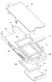
また、図2は、操作部側筐体部2の一部を分解した斜視図を示している。操作部側筐体部2は、図2に示すように、基板40と、RFID部41と、リアケース部42と、充電池43と、充電池カバー44と、によって構成されている。
FIG. 2 is an exploded perspective view of a part of the operation
基板40は、所定の演算処理を行うCPU等の素子が実装されており、表面部10上の操作ボタン群11がユーザにより操作が行われたときに、所定の信号がCPUに供給される。
The
RFID部41は、第1の使用周波数帯により外部装置と通信を行う磁界アンテナの一例であるループアンテナ50(第1のアンテナ部)と、ループアンテナ50により通信される情報に対して所定の処理を行うRFIDチップ51(第1の情報処理部)と、から構成されている。なお、RFID部41の詳細については後述する。また、RFIDチップ51は、基板40や図示しないサブ基板上に設けられていても良い。また、RFID部41は、ループアンテナ以外の磁界アンテナで構成されていても良い。
The
リアケース部42は、ヒンジ機構4を固定するヒンジ機構固定部42Aと、第1の使用周波数帯よりも高い周波数帯である第2の使用周波数帯により通信を行うメインアンテナ70(第2のアンテナ部)を収納するメインアンテナ収納部42Bと、充電池43を格納する充電池格納部42Cと、RFID部41を固定するRFID部固定部42Dとを備えている。なお、メインアンテナ70の詳細については後述する。
The
また、図3は、携帯電話装置1の機能を示す機能ブロック図である。携帯電話装置1は、図3に示すように、RFID部41により構成されている第1の通信部60と、外部の端末と通信を行う第2の通信部61と、第2の通信部61により通信される情報を処理する処理部62と、を備えている。
FIG. 3 is a functional block diagram showing functions of the
第1の通信部60は、上述したRFID部41により構成されており、第1の使用周波数帯(例えば、13.56MHz)により外部装置と通信を行うループアンテナ50と、RFIDチップ51と、調整用のコンデンサ52と、を備える。
The
ループアンテナ50は、例えば、PET(polyethylene terephthalate)材料からなるシート上に複数回渦巻き状に巻かれたコイルを備えて構成されており、外部装置から送信される第1の使用周波数帯の信号を受信する。
The
RFIDチップ51は、ループアンテナ50で受信された信号によって誘起された電力に基づいて所定の電圧を生成する電源回路53と、ループアンテナ50により通信される信号に対して変調処理又は復調処理等の信号処理を行うRF回路54と、所定の演算処理を行うCPU55と、所定のデータが格納されているメモリ56と、を備えている。電源回路53は、例えば、DC−DCコンバータにより構成されている。
The
ここで、第1の通信部60の動作について説明する。
Here, the operation of the
ループアンテナ50は、外部に設置されているリーダ・ライタ装置に対して、所定距離まで接近したときに、当該リーダ・ライタ装置から送信される電波(第1の使用周波数帯であるキャリア周波数(例えば、13.56MHz)により変調されている)を受信する。なお、コンデンサ52は、第1の使用周波数帯の電波がループアンテナ50を介してRF回路54に供給されるように、所定の調整(チューニング)を行う。
When the
また、ループアンテナ50により電波が受信されると、共振作用により起電力が発生する。
Further, when a radio wave is received by the
電源回路53は、共振作用により発生した起電力から所定の電源電圧を生成し、RF回路54と、CPU55と、メモリ56とに供給する。また、RF回路54と、CPU55と、メモリ56とは、電源回路53から所定の電源電圧が供給されることにより停止状態から起動状態に移行する。
The
RF回路54は、ループアンテナ50を介して供給された第1の使用周波数帯の信号に対して復調等の信号処理を行い、処理後の信号をCPU55に供給する。
The
CPU55は、RF回路54から供給された信号に基づいて、メモリ56にデータを書き込む、又は、メモリ56からデータを読み出す。CPU55は、メモリ56からデータを読み出した場合には、当該データをRF回路54に供給する。RF回路54は、メモリ56から読み出されたデータに対して変調等の信号処理を行い、ループアンテナ50を介して外部のリーダ・ライタ装置に送信する。
The
また、第1の通信部60は、上述では、電源部を有さない、いわゆる受動型(Passive)の誘導電磁界方式(電磁誘導方式)であるものとして説明を行ったが、これに限られず、受動型の相互誘導方式(電磁結合方式)又は放射電磁界方式(電波方式)であっても良いし、又は、電源部を有する能動型(Active)であっても良い。また、第1の通信部60のアクセス方式として、リード・ライト型であるものとして説明を行ったが、これに限られず、リードオンリー型や、ライトワンス型等であっても良い。
Further, in the above description, the
また、第2の通信部61は、図3に示すように、第1の使用周波数帯よりも高い周波数帯である第2の使用周波数帯により外部装置と通信を行うメインアンテナ70と、変調処理又は復調処理等の信号処理を行う通信処理部71(第2の情報処理部)と、を備える。また、第2の通信部61は、充電池43から電源の供給を受けている。
Further, as shown in FIG. 3, the
メインアンテナ70は、第2の使用周波数帯(例えば、800MHz)で外部装置と通信を行う。なお、本実施の形態では、第2の使用周波数帯として、800MHzとしたが、これ以外の周波数帯であっても良い。また、メインアンテナ70は、第2の使用周波数帯の他に、第3の使用周波数帯(例えば、2GHz)に対応できる、いわゆるデュアルバンド対応型による構成であっても良いし、さらに、第4の使用周波数帯にも対応できる複数バンド対応型により構成されていても良い。
The
通信処理部71は、メインアンテナ70によって受信した信号を復調処理し、処理後の信号を処理部62に供給し、処理部62から供給された信号を変調処理し、メインアンテナ70を介して外部装置に送信する。
The
また、処理部62は、図3に示すように、操作ボタン群11と、音声入力部12と、ディスプレイ21と、音声出力部22と、所定の演算処理を行うCPU72と、所定のデータが格納されているメモリ73と、所定の音処理を行う音響処理部74と、所定の画像処理を行う画像処理部75と、被写体を撮像するカメラモジュール76と、着信音等が出力されるスピーカ77と、を備えている。また、処理部62は、充電池43から電源の供給を受けている。なお、携帯電話装置1は、図3に示すように、CPU55とCPU72とが、信号線Sで結ばれており、信号線Sを介して第1の通信部60により処理された情報が画像処理部75に供給され、画像処理部75により処理された情報がディスプレイ21に表示される構成となっている。
Further, as shown in FIG. 3, the
また、図4は、RFID部41のループアンテナ50と、メインアンテナ70との位置関係を示す図である。なお、図4では、リアケース部42が省略されている。
FIG. 4 is a diagram showing a positional relationship between the
図4に示すように、ループアンテナ50と、メインアンテナ70とは、近接(数mm)して配置されている。このように、二つのアンテナが近接配置されていると、干渉による問題が生じる。
As shown in FIG. 4, the
具体的には、ループアンテナ50は、使用周波数帯(13.56MHz)以外に低次及び高次に周期的に副次共振点を有する。特に、高次の副次共振点(以下、高次共振点と呼ぶ。)がメインアンテナ70の使用周波数帯(800MHz)に重なってしまうと、メインアンテナ70の利得が劣化してしまう。
Specifically, the
そこで、本発明に係る携帯電話装置1では、ループアンテナ50の有する高次共振点によるメインアンテナ70への干渉を防ぎ、メインアンテナ70の利得劣化を回避するために、ループアンテナ50の高次共振点がメインアンテナ70の使用周波数帯に重ならないように、ループアンテナ50の一部分又は全体に亘って誘電体材料又は磁性体材料を貼付した構成、又はループアンテナ50の巻き数を変化させる構成になっている。
Therefore, in the
RFID部41では、ループアンテナ50のリアクタンス(L)値と、コンデンサ52のリアクタンス(C)値とにより共振(同調)周波数を調整し、13.56MHzに合わせている。ここで、L値は、ループアンテナ50の大きさや巻き数、又は、周囲に設けられている材料(磁性体や誘電体)の有無、若しくは周囲の金属との距離により決定される値である。また、高次共振点に関しては、ループアンテナ50のL値が支配的であり、このL値を変化させることにより、高次共振点の位置を調整することができる。なお、コンデンサ52のC値は、高次共振点に作用しない。
The
このようにして、携帯電話装置1では、ループアンテナ50の一部分又は全体に亘って誘電体材料又は磁性体材料を貼付又はループアンテナ50の巻き数を変化させることにより、ループアンテナ50のL値を調整して、ループアンテナ50の高次共振点をメインアンテナ70に重ならないように構成され、また、コンデンサ52のC値を調整することにより、13.56MHzに合わせるように構成されているので、使用周波数帯(13.56MHz)はそのままで、ループアンテナ50の高次共振点の位置をメインアンテナ70の使用周波数帯から外すことができる。
In this manner, in the
また、ループアンテナ50の一部分又は全体に亘って貼付される誘電体材料としては、PET材等のプラスチック、スポンジ、樹脂等を用いることができる。また、これらの材料は、比較的安価でありかつ軽量のため、携帯電話装置1の重量増を極力抑えることができる。
Moreover, as a dielectric material affixed over a part or the whole of the
ここで、ループアンテナ50の一部分又は全体に亘って誘電体材料又は磁性体材料を貼付した構成パターンを図5及び図6に示す。図5には、ループアンテナ50の4つの辺をそれぞれa辺、b辺、c辺及びd辺としたときの模式図を示し、図6には、図5に示したa辺乃至d辺のいずれの辺に誘電体材料又は磁性体材料を貼付するかの構成パターンを示す。
Here, FIG. 5 and FIG. 6 show a configuration pattern in which a dielectric material or a magnetic material is pasted over a part or the whole of the
図6に示すように、ループアンテナ50のa辺、b辺、c辺及びd辺に誘電体材料又は磁性体材料を貼付する構成パターンは、15通りある。
As shown in FIG. 6, there are 15 configuration patterns in which a dielectric material or a magnetic material is attached to the a side, the b side, the c side, and the d side of the
また、図7には、図6の「構成パターン15」に示すように、ループアンテナ50の全体に誘電体材料を貼付し、500MHz〜2.5GHzの周波数によりVSWR(Voltage Standing Wave Ratio)を測定したときの結果を示し、また、図8には、ループアンテナ50に誘電体材料を貼付せずに、500MHz〜2.5GHzの周波数によりVSWRを測定したときの結果を示す。なお、測定においては、携帯電話装置1のメインアンテナ70の給電点に測定装置(ネットワークアナライザ)を接続して行った。また、使用周波数帯の帯域幅が843MHz〜925MHz(図7及び図8中A点〜B点)と、1.92GHz〜2.18GHz(図7及び図8中C点〜D点)の携帯電話装置を使用して測定を行った。
Further, in FIG. 7, as shown in “
図7及び図8から分かるように、ループアンテナ50に誘電体材料を貼付しなかった場合(図8)には、843MHz〜925MHz(図8中A点〜B点)内にループアンテナ50の高次共振点の影響が現れているが(図8中X)、ループアンテナ50の全体に誘電体材料を貼付した場合(図7)には、843MHz〜925MHz(図7中A点〜B点)内にループアンテナ50の高次共振点の影響が消失している。
As can be seen from FIGS. 7 and 8, when the dielectric material is not attached to the loop antenna 50 (FIG. 8), the height of the
したがって、本発明によれば、ループアンテナ50の一部分又は全体に誘電体材料又は磁性体材料を貼付することにより、ループアンテナ50のL値を変化させ、ループアンテナ50の有する高次共振点の位置をずらすことができるので、メインアンテナ70への干渉を防ぐことができ、メインアンテナ70の利得劣化を回避することができる。また、本発明によれば、デザイン性を重視しつつ、筐体内のスペースを有効活用することができ、また、筐体自身の小型化を実現することができる。
Therefore, according to the present invention, the L value of the
また、上述したように、ループアンテナ50のL値は、巻き数によっても変えることができるので、巻き数を変化させる構成であっても良い。このように巻き数を変化させることにより、ループアンテナ50のL値を変化させ、ループアンテナ50の有する高次共振点の位置をずらすことができるので、メインアンテナ70への干渉を防ぐことができ、メインアンテナ70の利得劣化を回避することができる。
Further, as described above, since the L value of the
また、本実施形態のように電磁誘導方式により通信を行うループアンテナ50にあっては、その近傍に金属(例えば充電池43)が配設されると、通信する際に金属にも磁力線が入りこみ、これによって金属表面に電流(渦電流)が発生し、逆向きの磁力線が発生する場合がある。この逆向きに発生する磁力線は、ループアンテナ50の利得を低減させるおそれもあるが、本実施例のようにループアンテナ50の一部分又は全体に亘って誘電体材料又は磁性体材料を貼付することにより、この逆向きの磁力線は低減され、ループアンテナ50の利得の低減は好適に抑制される。
In addition, in the
また、このようにループアンテナ50の利得の低減が好適に抑制されることにより、ループアンテナ50自体の小型化も図られ、ひいてはループアンテナ50とメインアンテナ70の距離が好適に離間され、互いの干渉が好適に抑制される。
In addition, since the reduction of the gain of the
なお、上述した実施の形態では、メインアンテナ70と、ループアンテナ50とが近接配置により干渉が生じうる場合を想定したが、両アンテナの位置関係に係らず干渉が生じる場合にも本発明は有効である。
In the above-described embodiment, it is assumed that the
また、上述した実施の形態では、第1の使用周波数帯により外部機器と通信を行う構成要素としてRFIDを示したが、特にこれに限られず、メインアンテナ70の使用周波数帯に干渉が生じ得るような構成要素であれば他のものであっても良い。
In the above-described embodiment, RFID is shown as a component that communicates with an external device in the first used frequency band. However, the present invention is not limited to this, and interference may occur in the used frequency band of the
また、上述した実施の形態では、ループアンテナ50の一部分又は全体に亘って誘電体材料又は磁性体材料を貼付した構成又はループアンテナ50の巻き数を変化させる構成によりループアンテナ50の高次の副次共振点を調整する構成となっていたが、本発明はこれに限定されず、例えば、比透磁率の高い磁性粉末(フェライト粉末)をループアンテナ50に近接して形成された充電池カバー44や操作部側筐体部2の内部に練り込むことにより、ループアンテナ50の高次の副次共振点を調整する構成としても良い。これにより、磁性体材料を立体的にメインアンテナ70に近接させることができ、メインアンテナ70の利得劣化が好適に回避される。また、誘電体材料や磁性体材料をループアンテナ50の一部分又は全体に亘って貼付する必要がなくなるため、組み立ての容易化や設計の自由度の向上も図られる。
Further, in the above-described embodiment, a high-order sub antenna of the
また、磁性体材料は、メインアンテナ70に対して磁力線を収束させるという作用も奏するため、ループアンテナ50に近接して形成された充電池カバー44や操作部側筐体部2の内部に磁性体材料を練り込むことによりアンテナの受信感度性能の低下が効率良く抑制される。
Further, since the magnetic material also has an effect of converging the lines of magnetic force with respect to the
さらに、磁性粉末をループアンテナ50に近接して形成された充電池カバー44や操作部側筐体部2の内部に練り込むことにより、ループアンテナ50の近傍に配設された金属から発生する逆向きの磁力線も磁性粉末により好適に低減される。
Further, the magnetic powder is kneaded into the
<実施の形態2>
つぎに、本発明の実施の形態2について説明する。<
Next, a second embodiment of the present invention will be described.
メインアンテナ70の使用周波数によっては、メインアンテナ70の長さ(図9中のL)(例えば、4分の1波長(λ/4)分の長さ)と、ループアンテナ50のアンテナパターンにより形成される一辺の長さとが同等程度になる場合がある。このような場合において、メインアンテナ70と、ループアンテナ50とが近接して配置されると、ループアンテナ50の一辺がメインアンテナ70のイメージグランドとして見なされてしまい、メインアンテナ70の利得に影響を与えてしまう場合がある。
Depending on the operating frequency of the
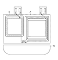
そこで、本発明では、図9に示すように、ループアンテナ50のアンテナパターンの一辺が最もメインアンテナ70に接近(対向)する辺(図中c辺)に対して、離調(オフセット)容量(離調コンデンサCm)を負荷するパターンを設け、そのリアクタンス(C)値を調整することによって高次の副次共振点を離調することにより、メインアンテナ70のアンテナ特性を調整する。
Therefore, in the present invention, as shown in FIG. 9, the detuning (offset) capacitance (with respect to the side (side c in the figure) where one side of the antenna pattern of the
このような構成にすることにより、離調コンデンサCmとループアンテナ50の一辺とにより形成されるLC共振回路は、メインアンテナ70の使用周波数付近でハイインピーダンスになるため、電流が流れなくなる。したがって、メインアンテナ70で使用周波数を受信する際に、ループアンテナ50の一辺がメインアンテナ70のイメージグランドとみなされなくなり、メインアンテナ70のアンテナ特性は劣化しない。なお、離調コンデンサCmのリアクタンス値は、コンデンサ52(Cf)に比べて十分に小さいものとする。
With this configuration, the LC resonance circuit formed by the detuning capacitor Cm and one side of the
つぎに、離調コンデンサCmを負荷することによる影響について以下に考察する。 Next, the effect of loading the detuning capacitor Cm will be considered below.
ループアンテナ50は、L値(L値は、ループアンテナ50の大きさや巻き数、磁性体や誘電体の有無及び周りの金属との距離により決定される。)と、基板上に配置されている調整用のコンデンサ52のリアクタンス(C)値により周波数を調整して、所定の共振周波数(例えば、13.56MHz)に同調させる。ここで、離調コンデンサCmは、上述したように、ループアンテナ50の同調容量に対して十分小さいため(Cf>>Cm)、ループアンテナ50の共振周波数には影響を与えない。
The
一方、上述したように、ループアンテナ50の高次共振点(メインアンテナ70の使用周波数帯)においては、ループアンテナ50のL値が支配的であり、このL値を変化させることで、高次共振点をずらすことが可能となる。したがって、コンデンサのリアクタンス(C)値は、高次共振点に作用しないので、離調コンデンサCmを負荷することの影響はない。
On the other hand, as described above, the L value of the
このようにして、本発明によれば、離調コンデンサCmを負荷することにより、メインアンテナ70のアンテナ特性を良好に保持しつつ、離調コンデンサCmの影響を排してループアンテナ50のアンテナ特性をも良好に保持することができる。
Thus, according to the present invention, by loading the detuning capacitor Cm, the antenna characteristics of the
なお、上述では、離調コンデンサCmは、ループアンテナ50のアンテナパターンの一辺が最もメインアンテナ70に接近する一つの辺(図中c辺)に対して設けられているものとして説明したが、これに限られず、全ての辺に対して設けられていても良い。
In the above description, the detuning capacitor Cm is described as being provided with respect to one side (c side in the figure) where one side of the antenna pattern of the
また、上述では、一つの離調コンデンサCmが、ループアンテナ50のアンテナパターンの一辺に対して接続されるように構成されていたが、本発明はこれに限定されず、一つの離調コンデンサCmが複数のループアンテナのいずれにも接続されるような構成であっても良い。
In the above description, one detuning capacitor Cm is configured to be connected to one side of the antenna pattern of the
例えば、カード機能とリーダ/ライタ機能の2つの機能を携帯無線機に持たせるべく、受動型のループアンテナと能動型のループアンテナの2つのアンテナがメインアンテナ70と併せて筐体内に配置されるような構成が考えられるが、このように複数のアンテナがメインアンテナ70と併せて筐体内に配設されるような構成であっても、一つの離調コンデンサCmがこれら複数のアンテナのいずれにも接続されることにより、複数のアンテナのそれぞれの高次共振点がメインアンテナの使用周波数帯から離調され、メインアンテナ70のアンテナ特性の低下が好適に抑制される。
For example, two antennas, a passive loop antenna and an active loop antenna, are arranged in the casing together with the
図10は、本構成の一例を示す図であり、本図では、受動型のループアンテナAと能動型のループアンテナBがメインアンテナ70と併せて筐体内に配設され、そのいずれもが一つの離調コンデンサCmに接続されている構成が示されている。このように受動型のループアンテナAと能動型のループアンテナBとがメインアンテナ70に近接して筐体内に配設されるような場合においては、受動型のループアンテナAと能動型のループアンテナBのそれぞれ高次共振点が、メインアンテナ70の使用周波数帯に干渉するおそれがあるが、一つの離調コンデンサCmが受動型のループアンテナAと能動型のループアンテナBのいずれにも接続されることにより、受動型のループアンテナAと能動型のループアンテナBのそれぞれの高次共振点がメインアンテナ70の使用周波数帯から離調され、もってメインアンテナ70のアンテナ特性の低下が好適に抑制される。
FIG. 10 is a diagram showing an example of this configuration. In this figure, a passive loop antenna A and an active loop antenna B are disposed in the casing together with the
また、一つの離調コンデンサCmにより複数のアンテナのそれぞれの高次共振点をまとめて調整することができるため、複数のアンテナ毎に高次共振点を調整するための手段を別途必要とせず、筐体内のスペースの効率化、部品点数の削減、筐体全体の小型化等も併せて図られることとなる。なお、複数のアンテナは2つのループアンテナに限らず、それ以上の数のその他のアンテナで構成されていても良い。 In addition, since each high-order resonance point of each of the plurality of antennas can be collectively adjusted by one detuning capacitor Cm, a means for adjusting the high-order resonance point for each of the plurality of antennas is not required. The efficiency of the space in the housing, the reduction in the number of parts, the miniaturization of the entire housing, and the like are also achieved. Note that the plurality of antennas is not limited to two loop antennas, and may be composed of a larger number of other antennas.
<実施の形態3>
つぎに、本発明の実施の形態3について説明する。<
Next, a third embodiment of the present invention will be described.
従来から、複数の使用周波数帯により外部と通信が可能ないわゆるマルチバンドアンテナを有する携帯無線機が知られている。このような携帯無線機においては、マルチバンドアンテナと他のアンテナとが近接配置されると、他のアンテナの高次の副次共振点が、マルチバンドアンテナの複数の使用周波数帯の全部又は一部に干渉し、マルチバンドアンテナの利得が劣化する場合がある。 2. Description of the Related Art Conventionally, portable radio devices having a so-called multiband antenna that can communicate with the outside using a plurality of use frequency bands are known. In such a portable wireless device, when a multiband antenna and another antenna are arranged close to each other, higher-order secondary resonance points of the other antennas are all or one of a plurality of use frequency bands of the multiband antenna. In some cases, the gain of the multiband antenna may deteriorate.
本実施の形態3に係る発明は、マルチバンドアンテナが通信を行う使用周波数帯に応じて、他のアンテナの高次の副次共振点を調整するため、マルチバンドアンテナの利得の劣化が低減される。 In the invention according to the third embodiment, the high-order secondary resonance point of another antenna is adjusted according to the use frequency band in which the multi-band antenna communicates, so that the deterioration of the gain of the multi-band antenna is reduced. The
図11は、マルチバンドアンテナを有する携帯電話装置100(携帯無線機)のブロック図である。携帯電話装置100は、図11に示すように、800MHzの使用周波数帯により外部と通信を行うメインアンテナ70(第1のアンテナ部)と、メインアンテナ70により通信される情報に対して所定の処理を行う通信処理部71の他、2GHzの使用周波数帯(第3の使用周波数帯)により外部と通信を行う第2のメインアンテナ80(第3のアンテナ部)と、第2のメインアンテナ80により通信される情報に対して所定の処理を行う通信処理部81(第3の通信処理部)を有して構成される。そして、通信処理部71及び通信処理部81は、いずれもCPU72(制御部)に接続されており、CPU72は、通信処理部71と通信処理部81のいずれか一方を制御可能に構成されている。また、第2のメインアンテナ80と通信処理部81とは、第3の通信部82を構成している。
FIG. 11 is a block diagram of a mobile phone device 100 (mobile radio) having a multiband antenna. As shown in FIG. 11, the
また、携帯電話装置100は、メインアンテナ70及び第2のメインアンテナ80の近傍に配置されるループアンテナ50を有する。ループアンテナ50は、メインアンテナ70及び第2のメインアンテナ80よりも低い使用周波数帯により外部と通信可能に構成されると共に、アンテナスイッチ部90を介してRF回路54と接続されて構成される。また、アンテナスイッチ部90は、CPU72に接続されている。また、CPU72は、現在、通信処理部71と通信処理部81のいずれを制御しているのかを示す制御信号をアンテナスイッチ部90に伝送する。すなわち、CPU72は、現在、第2の通信部61により通信が行われているときには通信処理部71を制御している旨を示す制御信号をアンテナスイッチ部90に伝送し、一方、現在、第3の通信部82により通信が行われているときには通信処理部81を制御している旨を示す制御信号をアンテナスイッチ部90に伝送する。アンテナスイッチ部90は、このCPU72から伝送される制御信号に応じてループアンテナ50とRF回路54とを接続する第1の経路91と第2の経路92とを選択的に切り換える。
In addition, the
第1の経路91には、ループアンテナ50の高次の副次共振点をメインアンテナ70の使用周波数帯である800MHz帯から離調させる離調手段A1が配設され、第2の経路92には、ループアンテナ50の高次の副次共振点が第2のメインアンテナ80の使用周波数帯である2GHz帯から離調させる離調手段A2が配設される。ここでの離調手段A1及びA2としては、ループアンテナ50のL値を変更可能に構成される誘電体材料、磁性体材料、離調コンデンサ等の他、ループアンテナ50の巻き数を変化させる導電体等が考えられる。なお、携帯電話装置100のその他の構成については、先の<実施の形態1>、<実施の形態2>において示した携帯電話装置1における構成と同じであるためそれらの説明は省略する。
The
また、携帯電話装置100は、これらの構成を有することにより、通信処理部71又は通信処理部81が通信を行う使用周波数帯に応じて、ループアンテナ50の高次の副次共振点を調整することができる。すなわち、CPU72は、通信処理部71により800MHzの使用周波数帯により外部と通信が行われた場合には、その旨を示す制御信号をアンテナスイッチ部90に伝送し、通信処理部81により2GHzの使用周波数帯により外部と通信が行われた場合には、その旨を示す制御信号をアンテナスイッチ部90に伝送する。
In addition, the
そして、アンテナスイッチ部90は、伝送された制御信号が通信処理部71による通信に係る信号であった場合には、ループアンテナ50とRF回路54とを第1の経路91で接続し、伝送された制御信号が通信処理部81による通信に係る信号であった場合には、ループアンテナ50とRF回路54とを第2の経路92で接続する。これにより、通信処理部71が800MHzの使用周波数帯により外部と通信をした場合には、ループアンテナ50とRF回路54とは第1の経路91で接続され、離調手段A1がループアンテナ50の高次の副次共振点を800MHz帯から離調させる。これにより、メインアンテナ70の利得の劣化は、好適に低減される。
Then, when the transmitted control signal is a signal related to communication by the
一方、通信処理部81が2GHzの使用周波数帯により外部と通信をした場合には、ループアンテナ50とRF回路54とは第2の経路92で接続され、離調手段A2がループアンテナ50の高次の副次共振点を2GHz帯から離調させる。これにより、第2のメインアンテナ80の利得の劣化は好適に低減される。
On the other hand, when the
なお、実施の形態3においては、マルチバンドアンテナとしてのメインアンテナ70と第2のメインアンテナ80とを別個の独立したアンテナであるとして説明したが、本発明のマルチバンドアンテナはこれに限らず、従来から知られているような、発信回路等を用いて複数の使用周波数帯により外部と通信可能な単一のアンテナであっても良い。なお、この場合のアンテナは、複数の周波数帯により通信される情報に対して所定の処理を行う単一の通信処理部を介して、当該単一の通信処理部を制御するCPU72に接続されているものとする。
In the third embodiment, the
Claims (10)
前記筐体内に配置される第1の使用周波数帯により外部と通信を行う第1のアンテナ部と、前記第1のアンテナ部により通信される情報に対して所定の処理を行う第1の情報処理部と、を有する第1の通信部と、
前記筐体内に配置される前記第1のアンテナ部の近傍に配置され、前記第1の使用周波数帯よりも高い周波数帯である第2の使用周波数帯により通信を行う第2のアンテナ部と、前記第2のアンテナ部により通信される情報に対して所定の処理を行う第2の情報処理部と、を有する第2の通信部と、を有し、
前記第1のアンテナ部の前記第2のアンテナ部に対する干渉が低減されるよう、前記第1のアンテナ部のリアクタンス成分が調整されることにより前記第1の使用周波数帯の高次の副次共振点が前記第2の使用周波数帯に重ならないように構成してあることを特徴とする携帯無線機。A housing,
A first antenna unit that communicates with the outside using a first use frequency band arranged in the housing, and a first information process that performs predetermined processing on information communicated by the first antenna unit A first communication unit having a unit;
A second antenna unit that is disposed in the vicinity of the first antenna unit disposed in the housing and performs communication in a second used frequency band that is a higher frequency band than the first used frequency band; A second communication unit having a second information processing unit that performs a predetermined process on information communicated by the second antenna unit;
The first to interference to the second antenna portion of the antenna portion is reduced, the first antenna portion reactance component of the high order of the first usable frequency band Symbol before Ri by to be adjusted A portable wireless device, wherein a secondary resonance point is configured not to overlap the second use frequency band.
前記磁界アンテナのL値が調整されることにより前記磁界アンテナのリアクタンス成分が調整され、前記副次共振点が前記第2の使用周波数帯に重ならないように構成してあることを特徴とする請求項1記載の携帯無線機。The first antenna unit is a magnetic field antenna,
The reactance component of the magnetic field antenna is adjusted by adjusting the L value of the magnetic field antenna, and the secondary resonance point is configured not to overlap the second use frequency band. Item 2. A portable wireless device according to Item 1.
前記磁界アンテナにコンデンサが接続されることにより前記磁界アンテナのリアクタンス成分が調整され、前記副次共振点が前記第2の使用周波数帯に重ならないように構成してあることを特徴とする請求項1記載の携帯無線機。The first antenna unit is a magnetic field antenna,
The reactance component of the magnetic field antenna is adjusted by connecting a capacitor to the magnetic field antenna, and the secondary resonance point is configured not to overlap the second use frequency band. The portable wireless device according to 1.
前記複数の磁界アンテナのいずれにもコンデンサが接続されることにより前記複数の磁界アンテナのリアクタンス成分が調整され、前記副次共振点が前記第2の使用周波数帯に重ならないように構成してあることを特徴とする請求項1記載の携帯無線機。The first antenna unit is a plurality of magnetic field antennas,
A reactance component of the plurality of magnetic field antennas is adjusted by connecting a capacitor to any of the plurality of magnetic field antennas, and the secondary resonance point is configured not to overlap the second use frequency band. The portable wireless device according to claim 1.
前記コンデンサは、前記第1のアンテナ部における前記第2のアンテナ部と対向する部分に接続される、ことを特徴とする請求項5記載の携帯無線機。The first antenna unit is arranged such that all or a part of the first antenna unit faces the second antenna unit in a predetermined direction,
6. The portable wireless device according to claim 5, wherein the capacitor is connected to a portion of the first antenna portion that faces the second antenna portion.
前記筐体内に配置される第1の使用周波数帯により外部と通信を行う第1のアンテナ部と、前記第1のアンテナ部により通信される情報に対して所定の処理を行う第1の情報処理部と、を有する第1の通信部と、
前記筐体内に配置される前記第1の使用周波数帯よりも高い周波数帯である第2の使用周波数帯により通信を行うと共に、前記第1のアンテナ部と干渉が生じ得る程度の位置に配された第2のアンテナ部と、前記第2のアンテナ部により通信される情報に対して所定の処理を行う第2の情報処理部と、を有する第2の通信部と、を有し、
前記第1のアンテナ部の前記第2のアンテナ部に対する干渉が低減されるよう、前記第1のアンテナ部のリアクタンス成分が調整されることにより前記第1のアンテナ部の共振によって生じる前記第1の使用周波数帯の高次の副次共振点が前記第2の使用周波数帯に重ならないように調整される構成であることを特徴とする携帯無線機。A housing,
A first antenna unit that communicates with the outside using a first use frequency band arranged in the housing, and a first information process that performs predetermined processing on information communicated by the first antenna unit A first communication unit having a unit;
The communication is performed in the second use frequency band that is higher than the first use frequency band arranged in the casing, and the communication unit is arranged at a position where interference with the first antenna unit may occur. A second communication unit including a second antenna unit, and a second information processing unit that performs predetermined processing on information communicated by the second antenna unit,
So that interference to the second antenna portion of the first antenna portion is reduced, resulting from the resonance of the first antenna portion of the reactance component is pre-Ri by the be adjusted Symbol first antenna portion and the portable radio, wherein the high-order secondary resonance point of the first usable frequency band is configured to be adjusted so that before Symbol does not overlap the second usable frequency band.
前記第2の通信部と前記第3の通信部のいずれか一方を制御すると共に、前記第2の通信部を制御する場合には前記第1の使用周波数帯の高次の副次共振点が前記第2の使用周波数帯に重ならないように調整し、前記第3の通信部を制御する場合には前記第1の使用周波数帯の高次の副次共振点が前記第3の使用周波数帯に重ならないように調整する制御部と、
を有することを特徴とする請求項1又は9に記載の携帯無線機。A third antenna unit that is disposed in the vicinity of the first antenna unit and performs communication in a third used frequency band that is a higher frequency body than the first used frequency band; and the third antenna unit. A third information processing unit that performs predetermined processing on information to be communicated;
When controlling one of the second communication unit and the third communication unit and controlling the second communication unit, a high-order secondary resonance point of the first used frequency band is When adjusting so as not to overlap the second used frequency band and controlling the third communication unit, a higher-order secondary resonance point of the first used frequency band is the third used frequency band. A control unit that adjusts so as not to overlap,
The portable wireless device according to claim 1, wherein the portable wireless device includes:
Priority Applications (1)
| Application Number | Priority Date | Filing Date | Title |
|---|---|---|---|
| JP2008537521A JP5192385B2 (en) | 2006-09-28 | 2007-09-28 | Portable radio |
Applications Claiming Priority (10)
| Application Number | Priority Date | Filing Date | Title |
|---|---|---|---|
| JP2006265215 | 2006-09-28 | ||
| JP2006265215 | 2006-09-28 | ||
| JP2007015537 | 2007-01-25 | ||
| JP2007015537 | 2007-01-25 | ||
| JP2007047209 | 2007-02-27 | ||
| JP2007047209 | 2007-02-27 | ||
| JP2007169905 | 2007-06-28 | ||
| JP2007169905 | 2007-06-28 | ||
| PCT/JP2007/069081 WO2008041652A1 (en) | 2006-09-28 | 2007-09-28 | Mobile radio device |
| JP2008537521A JP5192385B2 (en) | 2006-09-28 | 2007-09-28 | Portable radio |
Publications (2)
| Publication Number | Publication Date |
|---|---|
| JPWO2008041652A1 JPWO2008041652A1 (en) | 2010-02-04 |
| JP5192385B2 true JP5192385B2 (en) | 2013-05-08 |
Family
ID=39268511
Family Applications (1)
| Application Number | Title | Priority Date | Filing Date |
|---|---|---|---|
| JP2008537521A Expired - Fee Related JP5192385B2 (en) | 2006-09-28 | 2007-09-28 | Portable radio |
Country Status (4)
| Country | Link |
|---|---|
| US (1) | US8219143B2 (en) |
| JP (1) | JP5192385B2 (en) |
| KR (1) | KR101232557B1 (en) |
| WO (1) | WO2008041652A1 (en) |
Families Citing this family (19)
| Publication number | Priority date | Publication date | Assignee | Title |
|---|---|---|---|---|
| JP4924332B2 (en) * | 2007-09-27 | 2012-04-25 | 富士通東芝モバイルコミュニケーションズ株式会社 | Wireless system, wireless device, and antenna device |
| JP5159396B2 (en) * | 2008-04-03 | 2013-03-06 | キヤノン株式会社 | Communication device, control method thereof, and program |
| JP5197112B2 (en) * | 2008-04-04 | 2013-05-15 | キヤノン株式会社 | Communication device, control method thereof, and program |
| JP5150369B2 (en) * | 2008-05-28 | 2013-02-20 | 京セラ株式会社 | Communication equipment |
| JP5144419B2 (en) * | 2008-07-30 | 2013-02-13 | 京セラ株式会社 | Portable radio |
| JP5223584B2 (en) | 2008-10-14 | 2013-06-26 | 富士通モバイルコミュニケーションズ株式会社 | Wireless communication device |
| TWI400931B (en) * | 2008-12-29 | 2013-07-01 | Mstar Semiconductor Inc | Mobile communication device and communication method thereof |
| JP5468356B2 (en) * | 2009-10-28 | 2014-04-09 | 京セラ株式会社 | Mobile device |
| JP2011135447A (en) * | 2009-12-25 | 2011-07-07 | Sanyo Electric Co Ltd | Radio communication device |
| JP5619414B2 (en) * | 2009-12-25 | 2014-11-05 | 三洋電機株式会社 | Wireless communication device |
| JP5602484B2 (en) * | 2010-04-26 | 2014-10-08 | 京セラ株式会社 | Portable electronic devices |
| CN102122753A (en) | 2010-12-31 | 2011-07-13 | 惠州Tcl移动通信有限公司 | Near field communication electronic device and antennae thereof |
| US8982008B2 (en) * | 2011-03-31 | 2015-03-17 | Harris Corporation | Wireless communications device including side-by-side passive loop antennas and related methods |
| US9014761B2 (en) * | 2011-07-13 | 2015-04-21 | Lg Electronics Inc. | Mobile terminal |
| US9160079B2 (en) * | 2011-09-14 | 2015-10-13 | William N. Carr | Compact multi-band antenna |
| FR2984020B1 (en) * | 2011-12-13 | 2014-02-14 | Continental Automotive France | DEVICE AND METHOD FOR CONFIGURING ANTENNA |
| US8922348B2 (en) * | 2013-06-03 | 2014-12-30 | The Boeing Company | Radio frequency identification notification system |
| US9306283B2 (en) * | 2014-01-24 | 2016-04-05 | Sony Corporation | Antenna device and method for increasing loop antenna communication range |
| US12199359B2 (en) * | 2019-11-22 | 2025-01-14 | Lg Electronics Inc. | Antenna system mounted on vehicle |
Citations (6)
| Publication number | Priority date | Publication date | Assignee | Title |
|---|---|---|---|---|
| JP2001007629A (en) * | 1999-06-24 | 2001-01-12 | Sony Corp | Electronic device and information writing / reading device and method |
| JP2002032731A (en) * | 2000-07-14 | 2002-01-31 | Sony Corp | Contactless information exchange card |
| JP2005165703A (en) * | 2003-12-03 | 2005-06-23 | Hitachi Ltd | Non-contact identification medium |
| JP2005236585A (en) * | 2004-02-18 | 2005-09-02 | Sony Corp | Antenna module and portable information terminal having the same |
| JP2006165805A (en) * | 2004-12-03 | 2006-06-22 | Nec Saitama Ltd | Folding-type portable radio telephone set incorporated with contactless ic card function |
| JP2006211551A (en) * | 2005-01-31 | 2006-08-10 | Sony Ericsson Mobilecommunications Japan Inc | Mobile terminal |
Family Cites Families (11)
| Publication number | Priority date | Publication date | Assignee | Title |
|---|---|---|---|---|
| JPH0261675A (en) * | 1988-08-26 | 1990-03-01 | Minolta Camera Co Ltd | Developing device |
| JPWO2002061675A1 (en) | 2001-01-31 | 2004-06-03 | 株式会社ルネサステクノロジ | Non-contact identification medium |
| JP4071452B2 (en) * | 2001-04-13 | 2008-04-02 | 松下電器産業株式会社 | Portable radio |
| JP3678167B2 (en) * | 2001-05-02 | 2005-08-03 | 株式会社村田製作所 | ANTENNA DEVICE AND RADIO COMMUNICATION DEVICE HAVING THE ANTENNA DEVICE |
| JP4109029B2 (en) | 2002-07-19 | 2008-06-25 | 大日本印刷株式会社 | Mobile device with IC card replacement function |
| US6864843B2 (en) * | 2002-08-15 | 2005-03-08 | Paratek Microwave, Inc. | Conformal frequency-agile tunable patch antenna |
| FI114837B (en) * | 2002-10-24 | 2004-12-31 | Nokia Corp | Radio equipment and antenna structure |
| JP2004227046A (en) | 2003-01-20 | 2004-08-12 | Hitachi Ltd | Portable information equipment |
| JP3896989B2 (en) * | 2003-05-14 | 2007-03-22 | 三菱マテリアル株式会社 | Portable radio with RFID function |
| KR100542924B1 (en) | 2004-05-13 | 2006-01-11 | 주식회사 케이티프리텔 | RFID data processing method in mobile communication terminal and RFID terminal |
| KR20060088304A (en) * | 2005-02-01 | 2006-08-04 | 엘지전자 주식회사 | Mobile communication terminal supporting two different frequency bands |
-
2007
- 2007-09-28 WO PCT/JP2007/069081 patent/WO2008041652A1/en not_active Ceased
- 2007-09-28 JP JP2008537521A patent/JP5192385B2/en not_active Expired - Fee Related
- 2007-09-28 US US12/443,456 patent/US8219143B2/en not_active Expired - Fee Related
- 2007-09-28 KR KR1020097006235A patent/KR101232557B1/en not_active Expired - Fee Related
Patent Citations (6)
| Publication number | Priority date | Publication date | Assignee | Title |
|---|---|---|---|---|
| JP2001007629A (en) * | 1999-06-24 | 2001-01-12 | Sony Corp | Electronic device and information writing / reading device and method |
| JP2002032731A (en) * | 2000-07-14 | 2002-01-31 | Sony Corp | Contactless information exchange card |
| JP2005165703A (en) * | 2003-12-03 | 2005-06-23 | Hitachi Ltd | Non-contact identification medium |
| JP2005236585A (en) * | 2004-02-18 | 2005-09-02 | Sony Corp | Antenna module and portable information terminal having the same |
| JP2006165805A (en) * | 2004-12-03 | 2006-06-22 | Nec Saitama Ltd | Folding-type portable radio telephone set incorporated with contactless ic card function |
| JP2006211551A (en) * | 2005-01-31 | 2006-08-10 | Sony Ericsson Mobilecommunications Japan Inc | Mobile terminal |
Also Published As
| Publication number | Publication date |
|---|---|
| KR20090074747A (en) | 2009-07-07 |
| KR101232557B1 (en) | 2013-02-12 |
| US8219143B2 (en) | 2012-07-10 |
| WO2008041652A1 (en) | 2008-04-10 |
| JPWO2008041652A1 (en) | 2010-02-04 |
| US20100093390A1 (en) | 2010-04-15 |
Similar Documents
| Publication | Publication Date | Title |
|---|---|---|
| JP5192385B2 (en) | Portable radio | |
| JP5681010B2 (en) | Portable electronic devices | |
| JP5009361B2 (en) | Portable radio | |
| JP5153501B2 (en) | COMMUNICATION DEVICE AND COMMUNICATION DEVICE CONTROL METHOD | |
| JP5150369B2 (en) | Communication equipment | |
| JP5000701B2 (en) | Portable electronic device and magnetic field antenna circuit | |
| US7265720B1 (en) | Planar inverted-F antenna with parasitic conductor loop and device using same | |
| JP5602484B2 (en) | Portable electronic devices | |
| KR20020082787A (en) | Communication module and communication apparatus having such a communication module | |
| JP5117607B2 (en) | Portable radio | |
| JP4927162B2 (en) | Portable radio | |
| JP5144419B2 (en) | Portable radio | |
| JP2011165151A (en) | Radio communication device and noncontact communication antenna used for the same | |
| WO2006043543A1 (en) | Noncontact communication antenna and portable mobile terminal | |
| JP5787388B2 (en) | RADIO COMMUNICATION DEVICE AND NONCONTACT COMMUNICATION ANTENNA USED FOR THE RADIO COMMUNICATION DEVICE | |
| JP5289908B2 (en) | Communication equipment |
Legal Events
| Date | Code | Title | Description |
|---|---|---|---|
| A521 | Request for written amendment filed |
Free format text: JAPANESE INTERMEDIATE CODE: A523 Effective date: 20100819 |
|
| A521 | Request for written amendment filed |
Free format text: JAPANESE INTERMEDIATE CODE: A821 Effective date: 20100819 |
|
| A131 | Notification of reasons for refusal |
Free format text: JAPANESE INTERMEDIATE CODE: A131 Effective date: 20111213 |
|
| A521 | Request for written amendment filed |
Free format text: JAPANESE INTERMEDIATE CODE: A523 Effective date: 20120210 |
|
| A02 | Decision of refusal |
Free format text: JAPANESE INTERMEDIATE CODE: A02 Effective date: 20120619 |
|
| A521 | Request for written amendment filed |
Free format text: JAPANESE INTERMEDIATE CODE: A523 Effective date: 20120914 |
|
| A911 | Transfer to examiner for re-examination before appeal (zenchi) |
Free format text: JAPANESE INTERMEDIATE CODE: A911 Effective date: 20120925 |
|
| TRDD | Decision of grant or rejection written | ||
| A01 | Written decision to grant a patent or to grant a registration (utility model) |
Free format text: JAPANESE INTERMEDIATE CODE: A01 Effective date: 20130129 |
|
| A61 | First payment of annual fees (during grant procedure) |
Free format text: JAPANESE INTERMEDIATE CODE: A61 Effective date: 20130131 |
|
| R150 | Certificate of patent or registration of utility model |
Ref document number: 5192385 Country of ref document: JP Free format text: JAPANESE INTERMEDIATE CODE: R150 Free format text: JAPANESE INTERMEDIATE CODE: R150 |
|
| FPAY | Renewal fee payment (event date is renewal date of database) |
Free format text: PAYMENT UNTIL: 20160208 Year of fee payment: 3 |
|
| LAPS | Cancellation because of no payment of annual fees |