JP5175482B2 - Semiconductor device - Google Patents
Semiconductor device Download PDFInfo
- Publication number
- JP5175482B2 JP5175482B2 JP2007086385A JP2007086385A JP5175482B2 JP 5175482 B2 JP5175482 B2 JP 5175482B2 JP 2007086385 A JP2007086385 A JP 2007086385A JP 2007086385 A JP2007086385 A JP 2007086385A JP 5175482 B2 JP5175482 B2 JP 5175482B2
- Authority
- JP
- Japan
- Prior art keywords
- wiring
- semiconductor device
- semiconductor
- directional coupler
- region
- Prior art date
- Legal status (The legal status is an assumption and is not a legal conclusion. Google has not performed a legal analysis and makes no representation as to the accuracy of the status listed.)
- Expired - Fee Related
Links
- 239000004065 semiconductor Substances 0.000 title claims description 304
- 239000000758 substrate Substances 0.000 claims description 132
- 238000001514 detection method Methods 0.000 claims description 68
- 230000003321 amplification Effects 0.000 claims description 56
- 238000003199 nucleic acid amplification method Methods 0.000 claims description 56
- 230000015572 biosynthetic process Effects 0.000 claims description 30
- XUIMIQQOPSSXEZ-UHFFFAOYSA-N Silicon Chemical compound [Si] XUIMIQQOPSSXEZ-UHFFFAOYSA-N 0.000 claims description 15
- 229910052710 silicon Inorganic materials 0.000 claims description 15
- 239000010703 silicon Substances 0.000 claims description 15
- 238000004080 punching Methods 0.000 claims description 14
- 230000005669 field effect Effects 0.000 claims description 7
- 230000000149 penetrating effect Effects 0.000 claims description 3
- 239000010410 layer Substances 0.000 description 158
- VYPSYNLAJGMNEJ-UHFFFAOYSA-N Silicium dioxide Chemical compound O=[Si]=O VYPSYNLAJGMNEJ-UHFFFAOYSA-N 0.000 description 51
- 229910052814 silicon oxide Inorganic materials 0.000 description 51
- 238000000034 method Methods 0.000 description 49
- 230000008878 coupling Effects 0.000 description 38
- 238000010168 coupling process Methods 0.000 description 38
- 238000005859 coupling reaction Methods 0.000 description 38
- JBRZTFJDHDCESZ-UHFFFAOYSA-N AsGa Chemical compound [As]#[Ga] JBRZTFJDHDCESZ-UHFFFAOYSA-N 0.000 description 36
- 229910001218 Gallium arsenide Inorganic materials 0.000 description 35
- 239000012535 impurity Substances 0.000 description 27
- 239000010936 titanium Substances 0.000 description 21
- 229920002120 photoresistant polymer Polymers 0.000 description 19
- 238000004519 manufacturing process Methods 0.000 description 15
- 238000005229 chemical vapour deposition Methods 0.000 description 14
- RTAQQCXQSZGOHL-UHFFFAOYSA-N Titanium Chemical compound [Ti] RTAQQCXQSZGOHL-UHFFFAOYSA-N 0.000 description 13
- NRTOMJZYCJJWKI-UHFFFAOYSA-N Titanium nitride Chemical compound [Ti]#N NRTOMJZYCJJWKI-UHFFFAOYSA-N 0.000 description 13
- 238000005530 etching Methods 0.000 description 13
- 230000002829 reductive effect Effects 0.000 description 13
- 229910052719 titanium Inorganic materials 0.000 description 13
- WFKWXMTUELFFGS-UHFFFAOYSA-N tungsten Chemical compound [W] WFKWXMTUELFFGS-UHFFFAOYSA-N 0.000 description 13
- 229910052721 tungsten Inorganic materials 0.000 description 13
- 239000010937 tungsten Substances 0.000 description 13
- 229910021420 polycrystalline silicon Inorganic materials 0.000 description 12
- 229920005591 polysilicon Polymers 0.000 description 12
- 238000000206 photolithography Methods 0.000 description 11
- 238000002955 isolation Methods 0.000 description 10
- 230000036961 partial effect Effects 0.000 description 9
- 230000008569 process Effects 0.000 description 9
- 238000012545 processing Methods 0.000 description 9
- 230000005684 electric field Effects 0.000 description 8
- 229910052751 metal Inorganic materials 0.000 description 8
- 239000002184 metal Substances 0.000 description 8
- 229910052581 Si3N4 Inorganic materials 0.000 description 7
- 150000001875 compounds Chemical class 0.000 description 7
- 238000010586 diagram Methods 0.000 description 7
- 230000003071 parasitic effect Effects 0.000 description 7
- HQVNEWCFYHHQES-UHFFFAOYSA-N silicon nitride Chemical compound N12[Si]34N5[Si]62N3[Si]51N64 HQVNEWCFYHHQES-UHFFFAOYSA-N 0.000 description 7
- 238000005468 ion implantation Methods 0.000 description 6
- 238000010295 mobile communication Methods 0.000 description 6
- ZOXJGFHDIHLPTG-UHFFFAOYSA-N Boron Chemical compound [B] ZOXJGFHDIHLPTG-UHFFFAOYSA-N 0.000 description 5
- 229910052796 boron Inorganic materials 0.000 description 5
- 239000003990 capacitor Substances 0.000 description 5
- 239000001307 helium Substances 0.000 description 5
- 229910052734 helium Inorganic materials 0.000 description 5
- PXHVJJICTQNCMI-UHFFFAOYSA-N nickel Substances [Ni] PXHVJJICTQNCMI-UHFFFAOYSA-N 0.000 description 5
- 230000001413 cellular effect Effects 0.000 description 4
- 239000013078 crystal Substances 0.000 description 4
- 230000000694 effects Effects 0.000 description 4
- SWQJXJOGLNCZEY-UHFFFAOYSA-N helium atom Chemical compound [He] SWQJXJOGLNCZEY-UHFFFAOYSA-N 0.000 description 4
- 239000012212 insulator Substances 0.000 description 4
- 239000011229 interlayer Substances 0.000 description 4
- 238000000059 patterning Methods 0.000 description 4
- 230000001681 protective effect Effects 0.000 description 4
- 101001128814 Pandinus imperator Pandinin-1 Proteins 0.000 description 3
- 229910008807 WSiN Inorganic materials 0.000 description 3
- 229910052785 arsenic Inorganic materials 0.000 description 3
- RQNWIZPPADIBDY-UHFFFAOYSA-N arsenic atom Chemical compound [As] RQNWIZPPADIBDY-UHFFFAOYSA-N 0.000 description 3
- 238000004891 communication Methods 0.000 description 3
- 239000004020 conductor Substances 0.000 description 3
- 238000000151 deposition Methods 0.000 description 3
- 125000001475 halogen functional group Chemical group 0.000 description 3
- 230000005236 sound signal Effects 0.000 description 3
- 238000004544 sputter deposition Methods 0.000 description 3
- IJGRMHOSHXDMSA-UHFFFAOYSA-N Atomic nitrogen Chemical compound N#N IJGRMHOSHXDMSA-UHFFFAOYSA-N 0.000 description 2
- KRHYYFGTRYWZRS-UHFFFAOYSA-N Fluorane Chemical compound F KRHYYFGTRYWZRS-UHFFFAOYSA-N 0.000 description 2
- 101001024685 Pandinus imperator Pandinin-2 Proteins 0.000 description 2
- OAICVXFJPJFONN-UHFFFAOYSA-N Phosphorus Chemical compound [P] OAICVXFJPJFONN-UHFFFAOYSA-N 0.000 description 2
- BOTDANWDWHJENH-UHFFFAOYSA-N Tetraethyl orthosilicate Chemical compound CCO[Si](OCC)(OCC)OCC BOTDANWDWHJENH-UHFFFAOYSA-N 0.000 description 2
- FTWRSWRBSVXQPI-UHFFFAOYSA-N alumanylidynearsane;gallanylidynearsane Chemical compound [As]#[Al].[As]#[Ga] FTWRSWRBSVXQPI-UHFFFAOYSA-N 0.000 description 2
- 229910052782 aluminium Inorganic materials 0.000 description 2
- XAGFODPZIPBFFR-UHFFFAOYSA-N aluminium Chemical compound [Al] XAGFODPZIPBFFR-UHFFFAOYSA-N 0.000 description 2
- 230000008901 benefit Effects 0.000 description 2
- 239000010949 copper Substances 0.000 description 2
- 238000009792 diffusion process Methods 0.000 description 2
- 229910052738 indium Inorganic materials 0.000 description 2
- 238000002347 injection Methods 0.000 description 2
- 239000007924 injection Substances 0.000 description 2
- 238000012986 modification Methods 0.000 description 2
- 230000004048 modification Effects 0.000 description 2
- 229910021421 monocrystalline silicon Inorganic materials 0.000 description 2
- 229910052698 phosphorus Inorganic materials 0.000 description 2
- 239000011574 phosphorus Substances 0.000 description 2
- 238000005498 polishing Methods 0.000 description 2
- 230000008054 signal transmission Effects 0.000 description 2
- 239000000126 substance Substances 0.000 description 2
- 229910015900 BF3 Inorganic materials 0.000 description 1
- OKTJSMMVPCPJKN-UHFFFAOYSA-N Carbon Chemical compound [C] OKTJSMMVPCPJKN-UHFFFAOYSA-N 0.000 description 1
- RYGMFSIKBFXOCR-UHFFFAOYSA-N Copper Chemical compound [Cu] RYGMFSIKBFXOCR-UHFFFAOYSA-N 0.000 description 1
- 229910005540 GaP Inorganic materials 0.000 description 1
- UFHFLCQGNIYNRP-UHFFFAOYSA-N Hydrogen Chemical compound [H][H] UFHFLCQGNIYNRP-UHFFFAOYSA-N 0.000 description 1
- 230000001133 acceleration Effects 0.000 description 1
- 230000002411 adverse Effects 0.000 description 1
- 229910045601 alloy Inorganic materials 0.000 description 1
- 239000000956 alloy Substances 0.000 description 1
- QVGXLLKOCUKJST-UHFFFAOYSA-N atomic oxygen Chemical compound [O] QVGXLLKOCUKJST-UHFFFAOYSA-N 0.000 description 1
- IVHJCRXBQPGLOV-UHFFFAOYSA-N azanylidynetungsten Chemical compound [W]#N IVHJCRXBQPGLOV-UHFFFAOYSA-N 0.000 description 1
- WTEOIRVLGSZEPR-UHFFFAOYSA-N boron trifluoride Chemical compound FB(F)F WTEOIRVLGSZEPR-UHFFFAOYSA-N 0.000 description 1
- 229910052799 carbon Inorganic materials 0.000 description 1
- 239000000969 carrier Substances 0.000 description 1
- 230000015556 catabolic process Effects 0.000 description 1
- 230000008859 change Effects 0.000 description 1
- 239000002800 charge carrier Substances 0.000 description 1
- 229910052804 chromium Inorganic materials 0.000 description 1
- 238000004140 cleaning Methods 0.000 description 1
- 230000000295 complement effect Effects 0.000 description 1
- 239000000470 constituent Substances 0.000 description 1
- 229910052802 copper Inorganic materials 0.000 description 1
- 238000000354 decomposition reaction Methods 0.000 description 1
- 230000002542 deteriorative effect Effects 0.000 description 1
- 238000001312 dry etching Methods 0.000 description 1
- 230000005672 electromagnetic field Effects 0.000 description 1
- 230000005674 electromagnetic induction Effects 0.000 description 1
- 238000010893 electron trap Methods 0.000 description 1
- 239000000284 extract Substances 0.000 description 1
- HZXMRANICFIONG-UHFFFAOYSA-N gallium phosphide Chemical compound [Ga]#P HZXMRANICFIONG-UHFFFAOYSA-N 0.000 description 1
- -1 helium ions Chemical class 0.000 description 1
- 239000002784 hot electron Substances 0.000 description 1
- 239000001257 hydrogen Substances 0.000 description 1
- 229910052739 hydrogen Inorganic materials 0.000 description 1
- APFVFJFRJDLVQX-UHFFFAOYSA-N indium atom Chemical compound [In] APFVFJFRJDLVQX-UHFFFAOYSA-N 0.000 description 1
- 238000003780 insertion Methods 0.000 description 1
- 230000037431 insertion Effects 0.000 description 1
- 238000009413 insulation Methods 0.000 description 1
- 150000002500 ions Chemical class 0.000 description 1
- 239000000463 material Substances 0.000 description 1
- 229910044991 metal oxide Inorganic materials 0.000 description 1
- 150000004706 metal oxides Chemical class 0.000 description 1
- 229910052759 nickel Inorganic materials 0.000 description 1
- 150000004767 nitrides Chemical class 0.000 description 1
- 229910052757 nitrogen Inorganic materials 0.000 description 1
- 230000003647 oxidation Effects 0.000 description 1
- 238000007254 oxidation reaction Methods 0.000 description 1
- 229910052760 oxygen Inorganic materials 0.000 description 1
- 239000001301 oxygen Substances 0.000 description 1
- 230000001737 promoting effect Effects 0.000 description 1
- 230000002441 reversible effect Effects 0.000 description 1
- 239000002356 single layer Substances 0.000 description 1
Images


Classifications
-
- H—ELECTRICITY
- H10—SEMICONDUCTOR DEVICES; ELECTRIC SOLID-STATE DEVICES NOT OTHERWISE PROVIDED FOR
- H10D—INORGANIC ELECTRIC SEMICONDUCTOR DEVICES
- H10D84/00—Integrated devices formed in or on semiconductor substrates that comprise only semiconducting layers, e.g. on Si wafers or on GaAs-on-Si wafers
- H10D84/80—Integrated devices formed in or on semiconductor substrates that comprise only semiconducting layers, e.g. on Si wafers or on GaAs-on-Si wafers characterised by the integration of at least one component covered by groups H10D12/00 or H10D30/00, e.g. integration of IGFETs
- H10D84/82—Integrated devices formed in or on semiconductor substrates that comprise only semiconducting layers, e.g. on Si wafers or on GaAs-on-Si wafers characterised by the integration of at least one component covered by groups H10D12/00 or H10D30/00, e.g. integration of IGFETs of only field-effect components
- H10D84/83—Integrated devices formed in or on semiconductor substrates that comprise only semiconducting layers, e.g. on Si wafers or on GaAs-on-Si wafers characterised by the integration of at least one component covered by groups H10D12/00 or H10D30/00, e.g. integration of IGFETs of only field-effect components of only insulated-gate FETs [IGFET]
-
- H—ELECTRICITY
- H01—ELECTRIC ELEMENTS
- H01L—SEMICONDUCTOR DEVICES NOT COVERED BY CLASS H10
- H01L23/00—Details of semiconductor or other solid state devices
- H01L23/12—Mountings, e.g. non-detachable insulating substrates
-
- H—ELECTRICITY
- H01—ELECTRIC ELEMENTS
- H01L—SEMICONDUCTOR DEVICES NOT COVERED BY CLASS H10
- H01L23/00—Details of semiconductor or other solid state devices
- H01L23/58—Structural electrical arrangements for semiconductor devices not otherwise provided for, e.g. in combination with batteries
- H01L23/64—Impedance arrangements
- H01L23/66—High-frequency adaptations
-
- H—ELECTRICITY
- H01—ELECTRIC ELEMENTS
- H01P—WAVEGUIDES; RESONATORS, LINES, OR OTHER DEVICES OF THE WAVEGUIDE TYPE
- H01P5/00—Coupling devices of the waveguide type
- H01P5/12—Coupling devices having more than two ports
- H01P5/16—Conjugate devices, i.e. devices having at least one port decoupled from one other port
- H01P5/18—Conjugate devices, i.e. devices having at least one port decoupled from one other port consisting of two coupled guides, e.g. directional couplers
- H01P5/184—Conjugate devices, i.e. devices having at least one port decoupled from one other port consisting of two coupled guides, e.g. directional couplers the guides being strip lines or microstrips
-
- H—ELECTRICITY
- H10—SEMICONDUCTOR DEVICES; ELECTRIC SOLID-STATE DEVICES NOT OTHERWISE PROVIDED FOR
- H10D—INORGANIC ELECTRIC SEMICONDUCTOR DEVICES
- H10D84/00—Integrated devices formed in or on semiconductor substrates that comprise only semiconducting layers, e.g. on Si wafers or on GaAs-on-Si wafers
- H10D84/40—Integrated devices formed in or on semiconductor substrates that comprise only semiconducting layers, e.g. on Si wafers or on GaAs-on-Si wafers characterised by the integration of at least one component covered by groups H10D12/00 or H10D30/00 with at least one component covered by groups H10D10/00 or H10D18/00, e.g. integration of IGFETs with BJTs
- H10D84/401—Combinations of FETs or IGBTs with BJTs
- H10D84/403—Combinations of FETs or IGBTs with BJTs and with one or more of diodes, resistors or capacitors
-
- H—ELECTRICITY
- H10—SEMICONDUCTOR DEVICES; ELECTRIC SOLID-STATE DEVICES NOT OTHERWISE PROVIDED FOR
- H10D—INORGANIC ELECTRIC SEMICONDUCTOR DEVICES
- H10D84/00—Integrated devices formed in or on semiconductor substrates that comprise only semiconducting layers, e.g. on Si wafers or on GaAs-on-Si wafers
- H10D84/80—Integrated devices formed in or on semiconductor substrates that comprise only semiconducting layers, e.g. on Si wafers or on GaAs-on-Si wafers characterised by the integration of at least one component covered by groups H10D12/00 or H10D30/00, e.g. integration of IGFETs
- H10D84/811—Combinations of field-effect devices and one or more diodes, capacitors or resistors
-
- H—ELECTRICITY
- H01—ELECTRIC ELEMENTS
- H01L—SEMICONDUCTOR DEVICES NOT COVERED BY CLASS H10
- H01L2223/00—Details relating to semiconductor or other solid state devices covered by the group H01L23/00
- H01L2223/58—Structural electrical arrangements for semiconductor devices not otherwise provided for
- H01L2223/64—Impedance arrangements
- H01L2223/66—High-frequency adaptations
- H01L2223/6644—Packaging aspects of high-frequency amplifiers
-
- H—ELECTRICITY
- H01—ELECTRIC ELEMENTS
- H01L—SEMICONDUCTOR DEVICES NOT COVERED BY CLASS H10
- H01L2224/00—Indexing scheme for arrangements for connecting or disconnecting semiconductor or solid-state bodies and methods related thereto as covered by H01L24/00
- H01L2224/01—Means for bonding being attached to, or being formed on, the surface to be connected, e.g. chip-to-package, die-attach, "first-level" interconnects; Manufacturing methods related thereto
- H01L2224/42—Wire connectors; Manufacturing methods related thereto
- H01L2224/47—Structure, shape, material or disposition of the wire connectors after the connecting process
- H01L2224/48—Structure, shape, material or disposition of the wire connectors after the connecting process of an individual wire connector
- H01L2224/481—Disposition
- H01L2224/48151—Connecting between a semiconductor or solid-state body and an item not being a semiconductor or solid-state body, e.g. chip-to-substrate, chip-to-passive
- H01L2224/48221—Connecting between a semiconductor or solid-state body and an item not being a semiconductor or solid-state body, e.g. chip-to-substrate, chip-to-passive the body and the item being stacked
- H01L2224/48225—Connecting between a semiconductor or solid-state body and an item not being a semiconductor or solid-state body, e.g. chip-to-substrate, chip-to-passive the body and the item being stacked the item being non-metallic, e.g. insulating substrate with or without metallisation
- H01L2224/48227—Connecting between a semiconductor or solid-state body and an item not being a semiconductor or solid-state body, e.g. chip-to-substrate, chip-to-passive the body and the item being stacked the item being non-metallic, e.g. insulating substrate with or without metallisation connecting the wire to a bond pad of the item
-
- H—ELECTRICITY
- H01—ELECTRIC ELEMENTS
- H01L—SEMICONDUCTOR DEVICES NOT COVERED BY CLASS H10
- H01L2224/00—Indexing scheme for arrangements for connecting or disconnecting semiconductor or solid-state bodies and methods related thereto as covered by H01L24/00
- H01L2224/01—Means for bonding being attached to, or being formed on, the surface to be connected, e.g. chip-to-package, die-attach, "first-level" interconnects; Manufacturing methods related thereto
- H01L2224/42—Wire connectors; Manufacturing methods related thereto
- H01L2224/47—Structure, shape, material or disposition of the wire connectors after the connecting process
- H01L2224/49—Structure, shape, material or disposition of the wire connectors after the connecting process of a plurality of wire connectors
- H01L2224/491—Disposition
- H01L2224/4911—Disposition the connectors being bonded to at least one common bonding area, e.g. daisy chain
- H01L2224/49111—Disposition the connectors being bonded to at least one common bonding area, e.g. daisy chain the connectors connecting two common bonding areas, e.g. Litz or braid wires
-
- H—ELECTRICITY
- H01—ELECTRIC ELEMENTS
- H01L—SEMICONDUCTOR DEVICES NOT COVERED BY CLASS H10
- H01L2224/00—Indexing scheme for arrangements for connecting or disconnecting semiconductor or solid-state bodies and methods related thereto as covered by H01L24/00
- H01L2224/01—Means for bonding being attached to, or being formed on, the surface to be connected, e.g. chip-to-package, die-attach, "first-level" interconnects; Manufacturing methods related thereto
- H01L2224/42—Wire connectors; Manufacturing methods related thereto
- H01L2224/47—Structure, shape, material or disposition of the wire connectors after the connecting process
- H01L2224/49—Structure, shape, material or disposition of the wire connectors after the connecting process of a plurality of wire connectors
- H01L2224/491—Disposition
- H01L2224/4912—Layout
- H01L2224/49171—Fan-out arrangements
-
- H—ELECTRICITY
- H01—ELECTRIC ELEMENTS
- H01L—SEMICONDUCTOR DEVICES NOT COVERED BY CLASS H10
- H01L24/00—Arrangements for connecting or disconnecting semiconductor or solid-state bodies; Methods or apparatus related thereto
- H01L24/01—Means for bonding being attached to, or being formed on, the surface to be connected, e.g. chip-to-package, die-attach, "first-level" interconnects; Manufacturing methods related thereto
- H01L24/42—Wire connectors; Manufacturing methods related thereto
- H01L24/47—Structure, shape, material or disposition of the wire connectors after the connecting process
- H01L24/48—Structure, shape, material or disposition of the wire connectors after the connecting process of an individual wire connector
-
- H—ELECTRICITY
- H01—ELECTRIC ELEMENTS
- H01L—SEMICONDUCTOR DEVICES NOT COVERED BY CLASS H10
- H01L24/00—Arrangements for connecting or disconnecting semiconductor or solid-state bodies; Methods or apparatus related thereto
- H01L24/01—Means for bonding being attached to, or being formed on, the surface to be connected, e.g. chip-to-package, die-attach, "first-level" interconnects; Manufacturing methods related thereto
- H01L24/42—Wire connectors; Manufacturing methods related thereto
- H01L24/47—Structure, shape, material or disposition of the wire connectors after the connecting process
- H01L24/49—Structure, shape, material or disposition of the wire connectors after the connecting process of a plurality of wire connectors
-
- H—ELECTRICITY
- H01—ELECTRIC ELEMENTS
- H01L—SEMICONDUCTOR DEVICES NOT COVERED BY CLASS H10
- H01L2924/00—Indexing scheme for arrangements or methods for connecting or disconnecting semiconductor or solid-state bodies as covered by H01L24/00
- H01L2924/0001—Technical content checked by a classifier
- H01L2924/00014—Technical content checked by a classifier the subject-matter covered by the group, the symbol of which is combined with the symbol of this group, being disclosed without further technical details
-
- H—ELECTRICITY
- H01—ELECTRIC ELEMENTS
- H01L—SEMICONDUCTOR DEVICES NOT COVERED BY CLASS H10
- H01L2924/00—Indexing scheme for arrangements or methods for connecting or disconnecting semiconductor or solid-state bodies as covered by H01L24/00
- H01L2924/01—Chemical elements
- H01L2924/01019—Potassium [K]
-
- H—ELECTRICITY
- H01—ELECTRIC ELEMENTS
- H01L—SEMICONDUCTOR DEVICES NOT COVERED BY CLASS H10
- H01L2924/00—Indexing scheme for arrangements or methods for connecting or disconnecting semiconductor or solid-state bodies as covered by H01L24/00
- H01L2924/01—Chemical elements
- H01L2924/01029—Copper [Cu]
-
- H—ELECTRICITY
- H01—ELECTRIC ELEMENTS
- H01L—SEMICONDUCTOR DEVICES NOT COVERED BY CLASS H10
- H01L2924/00—Indexing scheme for arrangements or methods for connecting or disconnecting semiconductor or solid-state bodies as covered by H01L24/00
- H01L2924/01—Chemical elements
- H01L2924/01078—Platinum [Pt]
-
- H—ELECTRICITY
- H01—ELECTRIC ELEMENTS
- H01L—SEMICONDUCTOR DEVICES NOT COVERED BY CLASS H10
- H01L2924/00—Indexing scheme for arrangements or methods for connecting or disconnecting semiconductor or solid-state bodies as covered by H01L24/00
- H01L2924/01—Chemical elements
- H01L2924/01079—Gold [Au]
-
- H—ELECTRICITY
- H01—ELECTRIC ELEMENTS
- H01L—SEMICONDUCTOR DEVICES NOT COVERED BY CLASS H10
- H01L2924/00—Indexing scheme for arrangements or methods for connecting or disconnecting semiconductor or solid-state bodies as covered by H01L24/00
- H01L2924/049—Nitrides composed of metals from groups of the periodic table
- H01L2924/0494—4th Group
- H01L2924/04941—TiN
-
- H—ELECTRICITY
- H01—ELECTRIC ELEMENTS
- H01L—SEMICONDUCTOR DEVICES NOT COVERED BY CLASS H10
- H01L2924/00—Indexing scheme for arrangements or methods for connecting or disconnecting semiconductor or solid-state bodies as covered by H01L24/00
- H01L2924/10—Details of semiconductor or other solid state devices to be connected
- H01L2924/11—Device type
- H01L2924/12—Passive devices, e.g. 2 terminal devices
- H01L2924/1204—Optical Diode
- H01L2924/12041—LED
-
- H—ELECTRICITY
- H01—ELECTRIC ELEMENTS
- H01L—SEMICONDUCTOR DEVICES NOT COVERED BY CLASS H10
- H01L2924/00—Indexing scheme for arrangements or methods for connecting or disconnecting semiconductor or solid-state bodies as covered by H01L24/00
- H01L2924/10—Details of semiconductor or other solid state devices to be connected
- H01L2924/11—Device type
- H01L2924/13—Discrete devices, e.g. 3 terminal devices
- H01L2924/1304—Transistor
- H01L2924/1305—Bipolar Junction Transistor [BJT]
-
- H—ELECTRICITY
- H01—ELECTRIC ELEMENTS
- H01L—SEMICONDUCTOR DEVICES NOT COVERED BY CLASS H10
- H01L2924/00—Indexing scheme for arrangements or methods for connecting or disconnecting semiconductor or solid-state bodies as covered by H01L24/00
- H01L2924/10—Details of semiconductor or other solid state devices to be connected
- H01L2924/11—Device type
- H01L2924/13—Discrete devices, e.g. 3 terminal devices
- H01L2924/1304—Transistor
- H01L2924/1306—Field-effect transistor [FET]
- H01L2924/13091—Metal-Oxide-Semiconductor Field-Effect Transistor [MOSFET]
-
- H—ELECTRICITY
- H01—ELECTRIC ELEMENTS
- H01L—SEMICONDUCTOR DEVICES NOT COVERED BY CLASS H10
- H01L2924/00—Indexing scheme for arrangements or methods for connecting or disconnecting semiconductor or solid-state bodies as covered by H01L24/00
- H01L2924/19—Details of hybrid assemblies other than the semiconductor or other solid state devices to be connected
- H01L2924/1901—Structure
- H01L2924/1904—Component type
- H01L2924/19041—Component type being a capacitor
-
- H—ELECTRICITY
- H01—ELECTRIC ELEMENTS
- H01L—SEMICONDUCTOR DEVICES NOT COVERED BY CLASS H10
- H01L2924/00—Indexing scheme for arrangements or methods for connecting or disconnecting semiconductor or solid-state bodies as covered by H01L24/00
- H01L2924/19—Details of hybrid assemblies other than the semiconductor or other solid state devices to be connected
- H01L2924/191—Disposition
- H01L2924/19101—Disposition of discrete passive components
- H01L2924/19105—Disposition of discrete passive components in a side-by-side arrangement on a common die mounting substrate
-
- H—ELECTRICITY
- H01—ELECTRIC ELEMENTS
- H01L—SEMICONDUCTOR DEVICES NOT COVERED BY CLASS H10
- H01L2924/00—Indexing scheme for arrangements or methods for connecting or disconnecting semiconductor or solid-state bodies as covered by H01L24/00
- H01L2924/30—Technical effects
- H01L2924/301—Electrical effects
- H01L2924/30107—Inductance
-
- H—ELECTRICITY
- H01—ELECTRIC ELEMENTS
- H01L—SEMICONDUCTOR DEVICES NOT COVERED BY CLASS H10
- H01L2924/00—Indexing scheme for arrangements or methods for connecting or disconnecting semiconductor or solid-state bodies as covered by H01L24/00
- H01L2924/30—Technical effects
- H01L2924/301—Electrical effects
- H01L2924/3011—Impedance
- H01L2924/30111—Impedance matching
-
- H—ELECTRICITY
- H10—SEMICONDUCTOR DEVICES; ELECTRIC SOLID-STATE DEVICES NOT OTHERWISE PROVIDED FOR
- H10D—INORGANIC ELECTRIC SEMICONDUCTOR DEVICES
- H10D84/00—Integrated devices formed in or on semiconductor substrates that comprise only semiconducting layers, e.g. on Si wafers or on GaAs-on-Si wafers
- H10D84/01—Manufacture or treatment
- H10D84/0123—Integrating together multiple components covered by H10D12/00 or H10D30/00, e.g. integrating multiple IGBTs
- H10D84/0126—Integrating together multiple components covered by H10D12/00 or H10D30/00, e.g. integrating multiple IGBTs the components including insulated gates, e.g. IGFETs
- H10D84/013—Manufacturing their source or drain regions, e.g. silicided source or drain regions
- H10D84/0133—Manufacturing common source or drain regions between multiple IGFETs
-
- H—ELECTRICITY
- H10—SEMICONDUCTOR DEVICES; ELECTRIC SOLID-STATE DEVICES NOT OTHERWISE PROVIDED FOR
- H10D—INORGANIC ELECTRIC SEMICONDUCTOR DEVICES
- H10D84/00—Integrated devices formed in or on semiconductor substrates that comprise only semiconducting layers, e.g. on Si wafers or on GaAs-on-Si wafers
- H10D84/01—Manufacture or treatment
- H10D84/02—Manufacture or treatment characterised by using material-based technologies
- H10D84/03—Manufacture or treatment characterised by using material-based technologies using Group IV technology, e.g. silicon technology or silicon-carbide [SiC] technology
- H10D84/038—Manufacture or treatment characterised by using material-based technologies using Group IV technology, e.g. silicon technology or silicon-carbide [SiC] technology using silicon technology, e.g. SiGe
Landscapes
- Power Engineering (AREA)
- General Physics & Mathematics (AREA)
- Engineering & Computer Science (AREA)
- Computer Hardware Design (AREA)
- Microelectronics & Electronic Packaging (AREA)
- Physics & Mathematics (AREA)
- Condensed Matter Physics & Semiconductors (AREA)
- Amplifiers (AREA)
- Metal-Oxide And Bipolar Metal-Oxide Semiconductor Integrated Circuits (AREA)
- Semiconductor Integrated Circuits (AREA)
- Near-Field Transmission Systems (AREA)
- Transceivers (AREA)
- Control Of Amplification And Gain Control (AREA)
- Bipolar Transistors (AREA)
Description
本発明は、半導体装置に関し、特に、電力増幅機能を有する半導体装置に適用して有効な技術に関するものである。 The present invention relates to a semiconductor device, and more particularly to a technique effective when applied to a semiconductor device having a power amplification function.
特開2006−237238号公報(特許文献1)には、電力増幅回路を形成した半導体チップを実装基板上に搭載し、さらに、この実装基板内に方向性結合器(カプラ)を形成する技術が記載されている。
近年、GSM(Global System for Mobile Communications)方式、PCS(Personal Communication Systems)方式、PDC(Personal Digital Cellular)方式、およびCDMA(Code Division Multiple Access)方式といった通信方式に代表される移動体通信機器が世界的に普及している。一般に、この種の移動体通信機器は、電波の放射と受信をするアンテナ、電力変調された高周波信号を増幅してアンテナへ供給する高周波電力増幅器(RFパワーモジュール)、アンテナで受信した高周波信号を信号処理する受信部、これらの制御を行う制御部、そしてこれらに電源電圧を供給する電池(バッテリー)で構成される。 In recent years, mobile communication devices such as GSM (Global System for Mobile Communications), PCS (Personal Communication Systems), PDC (Personal Digital Cellular), and CDMA (Code Division Multiple Access) are widely used. Is popular. In general, this type of mobile communication device includes an antenna that radiates and receives radio waves, a high-frequency power amplifier (RF power module) that amplifies and supplies a power-modulated high-frequency signal to the antenna, and a high-frequency signal received by the antenna. A receiving unit that performs signal processing, a control unit that performs these controls, and a battery (battery) that supplies a power supply voltage thereto are configured.
移動体通信機器のRFパワーモジュールの電力増幅回路に用いられる増幅素子としては、HBT、HEMTなどの化合物半導体デバイス、シリコンバイポーラトランジスタ、LDMOSFET(Laterally Diffused Metal Oxide Semiconductor Field Effect Transistor、横方向拡散MOSFET)などが、目的や状況に応じて使用されている。 Amplifying elements used in power amplifier circuits of RF power modules of mobile communication devices include compound semiconductor devices such as HBT and HEMT, silicon bipolar transistors, LDMOSFETs (Laterally Diffused Metal Oxide Semiconductor Field Effect Transistors, lateral diffusion MOSFETs), etc. Are used according to purpose and situation.
また、近年、移動体通信機器の多機能化に伴って、RFパワーモジュールの小型化要求が強くなってきている。本発明者らは、RFパワーモジュールを小型化する技術について検討している。 In recent years, the demand for downsizing of the RF power module has increased with the increase in the number of functions of mobile communication devices. The present inventors have studied a technique for reducing the size of the RF power module.
RFパワーモジュールには、電力増幅回路が形成されており、この電力増幅回路で増幅された出力信号が送信される。このRFパワーモジュールは出力信号の電力を増幅する機能を有しており、出力電力は安定した一定出力である必要がある。RFパワーモジュールでは、電力増幅回路による出力電力の増幅を制御回路によって制御している。つまり、RFパワーモジュールでは、制御回路によって出力電力が一定になるように制御されるが、安定して一定になるとは限らない。このため、RFパワーモジュールには、出力電力を検出し、検出した出力電力に基づいてRFパワーモジュールから出力される出力電力が一定となるようにフィードバックする機能が設けられている。この出力電力を検出する部品は方向性結合器(カプラ)と呼ばれている。 In the RF power module, a power amplifier circuit is formed, and an output signal amplified by the power amplifier circuit is transmitted. This RF power module has a function of amplifying the power of the output signal, and the output power needs to be a stable and constant output. In the RF power module, amplification of output power by the power amplifier circuit is controlled by a control circuit. That is, in the RF power module, the output power is controlled to be constant by the control circuit, but it is not always stable and constant. For this reason, the RF power module is provided with a function of detecting output power and performing feedback so that the output power output from the RF power module is constant based on the detected output power. The component that detects the output power is called a directional coupler (coupler).
図32に示すように、方向性結合器102は、RFパワーモジュールを構成する実装基板100上に半導体チップ101とは別に整合回路などとともに実装されている。実装基板100上に方向性結合器102を形成する場合、実装基板100上の約1mm2程度の面積を方向性結合器102が占有することになる。したがって、同じく実装基板100上に搭載される整合回路とともに実装基板100の小型化を妨げる要因となっている。特に、近年、多機能化したRFパワーモジュールにおいては、実装基板100上の線路が密集しており、方向性結合器102を搭載する領域を確保することが困難になってきている。
As shown in FIG. 32, the
また、方向性結合器102を半導体チップ101とは別に実装基板100に搭載する場合、方向性結合器102で検出した電力を半導体チップ101に形成されている制御回路に戻す必要があり、方向性結合器102と半導体チップ101とをワイヤで接続する必要がある。このため、ワイヤボンディングする領域を確保する必要があり、実装基板100の小型化が困難になる。
When the
本発明の目的は、携帯電話機などに使用されるRFパワーモジュールの小型化を推進することのできる技術を提供することにある。 An object of the present invention is to provide a technique capable of promoting the miniaturization of an RF power module used for a mobile phone or the like.
本発明の前記ならびにその他の目的と新規な特徴は、本明細書の記述および添付図面から明らかになるであろう。 The above and other objects and novel features of the present invention will be apparent from the description of this specification and the accompanying drawings.
本願において開示される発明のうち、代表的なものの概要を簡単に説明すれば、次のとおりである。 Of the inventions disclosed in the present application, the outline of typical ones will be briefly described as follows.
本発明による半導体装置は、電力増幅回路を含む半導体チップを備え、前記半導体チップは、(a)半導体基板と、(b)前記半導体基板上に形成された前記電力増幅回路を構成するトランジスタと、(c)前記電力増幅回路から出力される出力電力を検出する方向性結合器とを有する。そして、前記方向性結合器は、(c1)前記トランジスタの出力配線を用いた主線路と、(c2)前記方向性結合器からの出力を電圧あるいは電流に変換する検波回路と第1端子が電気的に接続され、前記第1端子の他端である第2端子が受動素子を介してGNDと電気的に接続された副線路とを含む。ここで、前記主線路と前記副線路とは平行に配置され、かつ、前記主線路と前記副線路との間に導電体が存在しないことを特徴とするものである。 A semiconductor device according to the present invention includes a semiconductor chip including a power amplifier circuit, the semiconductor chip comprising: (a) a semiconductor substrate; and (b) a transistor forming the power amplifier circuit formed on the semiconductor substrate; (C) a directional coupler that detects output power output from the power amplifier circuit. The directional coupler includes: (c1) a main line using the output wiring of the transistor; (c2) a detection circuit that converts an output from the directional coupler into a voltage or a current; And a second terminal, which is the other end of the first terminal, includes a sub-line that is electrically connected to GND through a passive element. Here, the main line and the sub line are arranged in parallel, and no conductor exists between the main line and the sub line.
本願において開示される発明のうち、代表的なものによって得られる効果を簡単に説明すれば以下のとおりである。 Among the inventions disclosed in the present application, effects obtained by typical ones will be briefly described as follows.
方向性結合器を半導体チップ内に形成するので、携帯電話機などに使用されるRFパワーモジュールの小型化を推進することができる。 Since the directional coupler is formed in the semiconductor chip, it is possible to promote the miniaturization of the RF power module used for a mobile phone or the like.
以下の実施の形態においては便宜上その必要があるときは、複数のセクションまたは実施の形態に分割して説明するが、特に明示した場合を除き、それらはお互いに無関係なものではなく、一方は他方の一部または全部の変形例、詳細、補足説明等の関係にある。 In the following embodiments, when it is necessary for the sake of convenience, the description will be divided into a plurality of sections or embodiments. However, unless otherwise specified, they are not irrelevant to each other. There are some or all of the modifications, details, supplementary explanations, and the like.
また、以下の実施の形態において、要素の数等(個数、数値、量、範囲等を含む)に言及する場合、特に明示した場合および原理的に明らかに特定の数に限定される場合等を除き、その特定の数に限定されるものではなく、特定の数以上でも以下でもよい。 Further, in the following embodiments, when referring to the number of elements (including the number, numerical value, quantity, range, etc.), especially when clearly indicated and when clearly limited to a specific number in principle, etc. Except, it is not limited to the specific number, and may be more or less than the specific number.
さらに、以下の実施の形態において、その構成要素(要素ステップ等も含む)は、特に明示した場合および原理的に明らかに必須であると考えられる場合等を除き、必ずしも必須のものではないことは言うまでもない。 Further, in the following embodiments, the constituent elements (including element steps and the like) are not necessarily indispensable unless otherwise specified and apparently essential in principle. Needless to say.
同様に、以下の実施の形態において、構成要素等の形状、位置関係等に言及するときは、特に明示した場合および原理的に明らかにそうではないと考えられる場合等を除き、実質的にその形状等に近似または類似するもの等を含むものとする。このことは、上記数値および範囲についても同様である。 Similarly, in the following embodiments, when referring to the shapes, positional relationships, etc. of the components, etc., unless otherwise specified, and in principle, it is not considered that it is clearly apparent in principle. Including those that are approximate or similar to the shape. The same applies to the above numerical values and ranges.
また、実施の形態を説明するための全図において、同一の部材には原則として同一の符号を付し、その繰り返しの説明は省略する。なお、図面をわかりやすくするために平面図であってもハッチングを付す場合がある。以下に示す実施の形態で記載されているMOSFETは、MISFET(Metal Insulator Semiconductor Field Effect Transistor)の一例であり、本発明はゲート絶縁膜に酸化シリコン膜を使用する場合のほか、酸化シリコン膜よりも誘電率の高い高誘電率膜を使用する場合なども含まれる。 In all the drawings for explaining the embodiments, the same members are denoted by the same reference symbols in principle, and the repeated explanation thereof is omitted. In order to make the drawings easy to understand, even a plan view may be hatched. The MOSFET described in the following embodiment is an example of a MISFET (Metal Insulator Semiconductor Field Effect Transistor), and the present invention uses a silicon oxide film as a gate insulating film, as well as a silicon oxide film. The case where a high dielectric constant film having a high dielectric constant is used is also included.
(実施の形態1)
図1は、例えばデジタル携帯電話機における信号送受信部のブロック図を示したものである。図1において、携帯電話機における信号送受信部は、デジタル信号処理部1、IF(Intermediate Frequency)部2、変調信号源3、ミキサ4、RFパワーモジュール5、アンテナスイッチ6、アンテナ7、低雑音増幅器8を有している。
(Embodiment 1)
FIG. 1 shows a block diagram of a signal transmission / reception unit in a digital cellular phone, for example. In FIG. 1, a signal transmitting / receiving unit in a cellular phone includes a digital signal processing unit 1, an IF (Intermediate Frequency)
デジタル信号処理部1は、音声信号などのアナログ信号をデジタル処理してベースバンド信号を生成できるようになっており、IF部2は、デジタル信号処理部1で生成されたベースバンド信号を中間周波数の信号に変換することができるようになっている。
The digital signal processing unit 1 can generate a baseband signal by digitally processing an analog signal such as an audio signal, and the
変調信号源3は、周波数が安定な水晶発振器などの基準発振器を使用して変調信号を得るようにした回路であり、ミキサ4は、周波数を変換する周波数変換器である。
The
RFパワーモジュール5は、微弱な入力信号と相似な大電力の信号を電源から供給される電力で新たに生成して出力する回路である。 The RF power module 5 is a circuit that newly generates and outputs a high-power signal similar to a weak input signal with power supplied from a power source.
アンテナスイッチ6は、デジタル携帯電話機に入力される入力信号とデジタル携帯電話機から出力される出力信号とを分離するためのものである。 The antenna switch 6 is for separating an input signal input to the digital mobile phone and an output signal output from the digital mobile phone.
アンテナ7は、電波を送受信するためのものであり、低雑音増幅器8は、アンテナ7で受信した信号を増幅するためのものである。
The antenna 7 is for transmitting and receiving radio waves, and the
デジタル携帯電話機は、上記のように構成されており、以下に、その動作について簡単に説明する。まず、信号を送信する場合について説明する。デジタル信号処理部1で音声信号などのアナログ信号をデジタル処理することにより生成されたベースバンド信号は、IF部2において、中間周波数の信号に変換される。続いて、この中間周波数の信号は、変調信号源3およびミキサ4によって、無線周波数(RF(Radio Frequency)周波数)の信号に変換される。無線周波数に変換された信号は、RFパワーモジュール5に入力される。RFパワーモジュール5に入力した無線周波数の信号は、RFパワーモジュール5で増幅された後、アンテナスイッチ6を介してアンテナ7より送信される。
The digital cellular phone is configured as described above, and its operation will be briefly described below. First, a case where a signal is transmitted will be described. A baseband signal generated by digitally processing an analog signal such as an audio signal in the digital signal processing unit 1 is converted into an intermediate frequency signal in the
次に、信号を受信する場合について説明する。アンテナ7により受信された無線周波数の信号は、低雑音増幅器8で増幅される。続いて、低雑音増幅器8で増幅された信号は、変調信号源3およびミキサ4によって、中間周波数の信号に変換された後、IF部2に入力される。IF部2では、中間周波数の信号の検波が行なわれ、ベースバンド信号が抽出される。その後、このベースバンド信号は、デジタル信号処理部1で処理され、音声信号が出力される。
Next, a case where a signal is received will be described. The radio frequency signal received by the antenna 7 is amplified by the
上述したように、デジタル携帯電話機から信号を送信する際、RFパワーモジュール5によって信号は増幅される。次に、このRFパワーモジュール5の構成について説明する。図2は、本実施の形態1のRFパワーモジュールにおける高周波増幅回路の回路ブロックを示したものである。図2を参照しながら、高周波増幅回路の回路ブロックについて説明する。 As described above, when the signal is transmitted from the digital mobile phone, the signal is amplified by the RF power module 5. Next, the configuration of the RF power module 5 will be described. FIG. 2 shows a circuit block of a high-frequency amplifier circuit in the RF power module of the first embodiment. The circuit block of the high frequency amplifier circuit will be described with reference to FIG.
図2において、RFパワーモジュール5に形成されている高周波増幅回路は、実装基板10上に搭載された半導体チップ11と実装基板上に搭載された整合回路12a、12bから構成されている。そして、半導体チップ11には、増幅回路13aと増幅回路13bが形成されている。増幅回路13aは、第1の周波数を利用しており、GSM(Global System for Mobile Communication)方式の利用で、周波数としてはGSM低周波帯域の824MHz〜915MHzを使用している信号を増幅できるようになっている。また、増幅回路13bは、第2の周波数を利用していてGSM高周波帯域の1710MHz〜1910MHzを使用している信号を増幅できるようになっている。このように、本実施の形態1では、半導体チップ11に異なる2つの周波数帯の信号を増幅することができるようになっている。
In FIG. 2, the high-frequency amplifier circuit formed in the RF power module 5 includes a
増幅回路13aは、増幅部14a、バイアス回路15a、方向性結合器16aおよび検波回路17aを有している。同様に、増幅回路13bは、増幅部14b、バイアス回路15b、方向性結合器16bおよび検波回路17bを有している。さらに、半導体チップ11の内部には、バンド切換スイッチ18、19と差動増幅器20が形成されている。
The
増幅部14aは、端子Pin1から入力されるGSM方式低周波帯域の入力信号を増幅するアンプであり、例えば、3つの増幅段で構成されている。同様に、増幅部14bは、端子Pin2から入力されるGSM方式高周波帯域の入力信号を増幅するアンプであり、例えば、3つの増幅段で構成されている。
The amplifying
バイアス回路15aは、端子Vapcから入力されるパワー制御電圧にしたがって増幅部14aにバイアス電圧を印加して増幅度を制御するように構成されており、制御回路になっている。同様に、バイアス回路15bは、端子Vapcから入力されるパワー制御電圧にしたがって増幅部14bにバイアス電圧を印加して増幅度を制御するように構成されており、制御回路になっている。
The
方向性結合器16a、16bは、増幅部14a、14bで増幅された信号の電力を検出できるように構成されており、本実施の形態1では、この方向性結合器16a、16bが半導体チップ11の内部に形成されている点に特徴の1つがある。つまり、従来技術では、方向性結合器16a、16bは半導体チップ11を搭載している実装基板10上に整合回路12a、12bとともに形成されていたが、本実施の形態1では、方向性結合器16a、16bを半導体チップ11内に形成している。これにより、実装基板10上に方向性結合器16a、16bを搭載するスペースを確保する必要がなくなり、実装基板10の小型化を図ることができる。
The
検波回路17a、17bは、方向性結合器16a、16bにより検出された電力を電圧あるいは電流に変換して差動増幅器20に出力するように構成されている。
The
バンド切換スイッチ18、19は、GSM方式低周波帯域の信号を増幅する増幅部14aとGSM方式高周波帯域の信号を増幅する増幅部14bとの動作切換を行なうように構成されており、図示しないバンド切換信号によって制御されるようになっている。
The band changeover switches 18 and 19 are configured to switch operation between an
差動増幅器20は、端子Vapcから入力されるパワー制御電圧と検波回路17a、17bから出力される電圧との差分を検出するように構成されている。以上が半導体チップ11の内部に形成されている回路であり、半導体チップ11の外部にある実装基板10上には、整合回路12a、12bが形成されている。整合回路12a、12bは、増幅回路13a、13bで増幅された信号が反射されずに効率よく出力できるように、受動素子を用いてインピーダンスが調整されている。すなわち、整合回路12a、12bは、それぞれ増幅回路13a、13bから出力される信号に対してインピーダンス整合するように構成されている。具体的に、整合回路12a、12bは、抵抗素子、容量素子、インダクタンス素子などを用いて形成されている。
The
本実施の形態1における高周波増幅回路は上記のように構成されており、以下にその動作について説明する。本実施の形態1では、GSM方式低周波帯域および高周波帯域の信号を増幅することができるように構成されているが、動作は同様なので低周波帯域の信号を増幅する動作について説明する。また、通信方式はGSM方式について説明しているが、他の通信方式であってもよい。 The high frequency amplifier circuit according to the first embodiment is configured as described above, and the operation thereof will be described below. Although the first embodiment is configured to amplify signals in the GSM low frequency band and high frequency band, the operation is the same, and therefore the operation for amplifying the low frequency band signal will be described. Further, although the GSM method has been described as the communication method, other communication methods may be used.
まず、バンド切換信号によってバンド切換スイッチ18、19は増幅回路13aを動作させるように切り換えられる。その後、端子Pin1から入力された入力信号が増幅部14aに入力する。また、端子Vapcからはパワー制御電圧がバイアス回路15aに入力され、このパワー制御電圧に基づいてバイアス回路15aが増幅部14aにバイアス電圧を印加する。すると、増幅部14aは、バイアス回路15aからのバイアス電圧に基づいて入力信号を増幅して信号を出力する。増幅部14aで増幅された信号は、半導体チップ11から出力され実装基板10に搭載されている整合回路12aに入力する。整合回路12aではインピーダンス整合しているため、増幅された信号が反射せずに効率良く端子Pout1から出力される。このようにして、端子Pout1から所望の信号が出力される。
First, the band changeover switches 18 and 19 are switched by the band changeover signal so as to operate the
端子Pout1からは一定電力の信号が出力されることが望ましい。しかし、外部からの影響などにより実際に出力される信号の電力が所望の電力になっているとは限らない。そこで、増幅部14aを制御するバイアス回路15aにフィードバックをかけて出力電力を制御する回路を設けている。このフィードバック回路の動作について説明する。増幅部14aで増幅された信号の電力は、増幅部14aと整合回路12aとの間に設けられた方向性結合器16aによって検出される。方向性結合器16aで検出された電力は、方向性結合器16aに接続されている検波回路17aで電圧に変換される。検波回路17aで変換された電圧は、差動増幅器20に入力する。一方、差動増幅器20には、端子Vapcから入力したパワー制御電圧も入力する。そして、差動増幅器20では、検波回路17aで変換された電圧とパワー制御電圧との差分が検出される。次に、差動増幅器20で検出された差分がなくなるようにバイアス回路15aから増幅部14aに印加するバイアス電圧の大きさが制御される。これにより、端子Pout1から出力される信号の電力が一定となる。このようにして、RFパワーモジュールに形成されている高周波増幅回路が動作する。
It is desirable that a signal of constant power is output from the terminal Pout1. However, the power of the signal that is actually output is not always the desired power due to external influences. Therefore, a circuit for controlling the output power by providing feedback to the
次に、方向性結合器16aについて説明する。図3は、方向性結合器16aの構成を示す模式図である。図3に示すように、方向性結合器16aは、主線路を構成する配線と副線路を構成する配線から構成されている。この方向性結合器16aは、四端子素子であり、主線路を進行する電力を電磁界結合によって副線路で検出するものである。このため、主線路と副線路とは平行に配置されており、主線路と副線路との間には導電体が存在しないように構成されている。
Next, the
方向性結合器16aの性能を示すものとして結合度と方向性というものがある。結合度とは、主線路を進行する電力に対して副線路で検出される電力の度合いを示したものであり、結合度が大きければ大きいほど主線路を進行する電力に対して副線路で検出する電力の大きさが大きくなる。方向性結合器16aの結合度は、平行に配置されている主線路と副線路の長さが長く、また、主線路と副線路との間の距離が小さいほど向上させることができる。
Examples of the performance of the
続いて、方向性結合器16aの方向性について説明する。図3に示すように、主線路の一端をPort1とし、他端をPort2とする。また、副線路の一端をPort3とし、他端をPort4とする。いま、主線路のPort1からPort2に向って電力(高周波信号)が進行するとする。つまり、図2との対応を考えると、主線路のPort1は増幅部14aに接続され、主線路のPort2は整合回路12aに接続されている。整合回路12aによるインピーダンス整合がなされていない場合には、主線路のPort1からPort2に向って進む電力と、Port2側で反射してPort2からPort1に進む電力が混在することになる。しかし、実際の回路では、整合回路12aによってインピーダンス整合が取られているので、Port2側で反射してPort2からPort1に進む電力は存在しないと考えることができる。すなわち、主線路には、Port1からPort2に進む電力だけが存在することになる。
Next, the directionality of the
このように主線路を進行する電力の電磁界結合によって副線路側に電力が発生するが、電磁界結合には、電界結合と磁界結合が含まれている。主線路と副線路との電界結合は、主線路と副線路間の容量に起因して発生し、電界結合によって副線路で検出される電力は、副線路のPort3とPort4に均等に進む。つまり、電界結合に起因した電力は向きを持たない。一方、主線路と副線路との磁界結合は、主線路と副線路との間の電磁誘導現象によって発生するため、磁界結合に起因して検出される電力は、発生している磁界を打ち消す向きに現れる。つまり、磁界結合に起因した電力は特定方向に進む。したがって、例えば、電界結合によって副線路のPort4に進む電力と磁界結合によって副線路のPort3に進む電力が釣り合えば、副線路のPort4には電力が発生しなくなる。このように、副線路のPort4で電界結合に起因した電力と磁界結合に起因した電力が釣り合うように構成することで、副線路のPort3に進む電力だけが検出される。これにより、特定方向に進む電力だけを検出する方向性結合器16aが実現される。
As described above, electric power is generated on the side of the sub line by electromagnetic coupling of electric power traveling through the main line. The electromagnetic coupling includes electric field coupling and magnetic field coupling. The electric field coupling between the main line and the sub-line occurs due to the capacitance between the main line and the sub-line, and the power detected in the sub-line by the electric field coupling travels equally to
ここで、副線路のPort4において、電界結合に起因した電力と磁界結合に起因した電力が釣り合うように構成するために、副線路のPort4には所定の受動素子(抵抗、容量、インダクタなど)を介してGND電位に接続されている。この受動素子のインピーダンスが所定値になるように選択することにより、副線路のPort4において、電界結合に起因した電力と磁界結合に起因した電力が釣り合うようにすることができる。 Here, in the Port 4 of the sub line, in order to configure the power caused by the electric field coupling and the power caused by the magnetic field coupling to be balanced, a predetermined passive element (resistor, capacitor, inductor, etc.) is provided in the Port 4 of the sub line. To the GND potential. By selecting the impedance of the passive element to be a predetermined value, it is possible to balance the power caused by the electric field coupling and the power caused by the magnetic field coupling at the Port 4 of the sub line.
上記のように構成された方向結合器16aによれば、副線路のPort3へ検出された電力が進む。この電力は図2に示す検波回路17aで、例えば、電圧に変換される。すなわち、方向性結合器16aのPort3は検波回路17aと電気的に接続されている。次に、この検波回路17aの回路構成の一例について説明する。
According to the
図4は、検波回路17aの回路構成例を示す図である。図4において、検波回路17aは、nチャネル型MOSFET(Metal Insulator Semiconductor Field Effect Transistor)21、24およびpチャネル型MOSFET22、23を有している。nチャネル型MOSFET21とpチャネル型MOSFET22は、GND電位と電源電位(Vdd)との間に直列に接続されている。さらに、GND電位と電源電位との間には、直列に接続されたpチャネル型MOSFET23とnチャネル型MOSFET24が直列に接続されたnチャネル型MOSFET21とpチャネル型MOSFET22と並列になるように接続されている。
FIG. 4 is a diagram illustrating a circuit configuration example of the
pチャネル型MOSFET22のゲート電極とpチャネル型MOSFET23のゲート電極は接続されており、これらのゲート電極はpチャネル型MOSFET22のドレイン領域に接続されている。これにより、pチャネル型MOSFET22とpチャネル型MOSFET23によりカレントミラー回路が構成される。また、nチャネル型MOSFET24のゲート電極もnチャネル型MOSFET24のドレイン領域と電気的に接続されている。
The gate electrode of the p-
このように構成された検波回路17aの動作について説明する。まず、方向性結合器により検出された電力(高周波信号)が検波回路17aの入力端子に入力する。検波回路17aの入力端子に入力した電力は、nチャネル型MOSFET21のゲート電極に入力する。すると、ゲート電極に入力した電力の振幅に対応した電流がnチャネル型MOSFET21のソース領域とドレイン領域の間に流れる。このとき、pチャネル型MOSFET22とpチャネル型MOSFET23で構成されたカレントミラー回路により、nチャネル型MOSFET24のソース領域とドレイン領域の間にもnチャネル型MOSFET21のソース領域とドレイン領域の間に流れる電流と同量の電流が流れる。したがって、nチャネル型MOSFET24のソース領域とドレイン領域に同量の電流を流すために必要な電圧が検波回路17aの出力端子に発生する。このように検波回路17aによって方向性結合器により検出された電力を電圧に変換することができる。
The operation of the
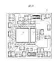
次に、本実施の形態1におけるRFパワーモジュールの実装構成について説明する。図5は、本実施の形態1におけるRFパワーモジュールの実装構成を示した平面図である。図5に示すように、本実施の形態1におけるRFパワーモジュールは、実装基板(配線基板)10上に半導体チップ11と受動部品が搭載されている。実装基板10は、例えばプリント配線基板から構成されており、複数の誘電体層(絶縁層)を貼り合せた構造をしている。この実装基板10には、表面(主面)や裏面および内部に所定の配線が形成されているとともに、実装基板10の表面に形成された一部の配線と実装基板10の裏面に形成された一部の配線とは、実装基板10の厚さ方向に形成されたビアを介して電気的に接続されている。
Next, the mounting configuration of the RF power module according to the first embodiment will be described. FIG. 5 is a plan view showing the mounting configuration of the RF power module according to the first embodiment. As shown in FIG. 5, the RF power module according to the first embodiment has a
半導体チップ11は、シリコンを主成分とするものであり、シリコン基板上に図2に示す増幅回路13a、13b、バンド切換スイッチ18、19および差動増幅器20などが形成されている。増幅回路13a、13bを構成する要素としては、増幅部14a、14b、バイアス回路15a、15b、方向性結合器16a、16bおよび検波回路17a、17bなどがある。
The
増幅部14a、14bは、例えば、3つの増幅段で構成されており、それぞれの増幅段は、シリコン基板上に形成されるLDMOSFETから形成されている。また、バイアス回路15a、15b、検波回路17a、17b、バンド切換スイッチ18、19および差動増幅器20は、シリコン基板上に形成されるMOSFETなどから形成される。
The amplifying
この半導体チップ11は四角形状をしており、外周部に沿って複数のボンディングパッド(図示せず)が形成されている。これらのボンディングパッドと実装基板10上に形成されている端子がワイヤなどで接続されている。
The
実装基板10上に形成されている受動部品は、例えばチップ部品から構成され、抵抗、インダクタンス素子、コンデンサなどが含まれる。これらの受動部品は、配線基板の表面に形成された配線と電気的に接続されている。受動部品は、例えば図2に示す整合回路12a、12bなどを構成している。
The passive component formed on the mounting
ここで、本実施の形態1における特徴の1つは、半導体チップ11の内部に方向性結合器16a、16bを設けている点にある。つまり、本実施の形態1では、半導体チップ11を構成するシリコン基板上に方向性結合器16a、16bが形成されている。従来、図32に示すように、方向性結合器102は半導体チップ101の内部ではなく、半導体チップ101の外部にある実装基板100上に搭載されていた。このため、実装基板100上に方向性結合器102を搭載する領域を確保する必要があり、実装基板100の小型化の妨げになっている。特に、異なる周波数帯域の信号を増幅するRFパワーモジュールでは、複数の方向性結合器102を搭載する必要があるため、方向性結合器102の実装基板100に占める面積が大きくなる。
Here, one of the features in the first embodiment is that
これに対し、本実施の形態1では、図5に示すように、半導体チップ11の内部に方向性結合器を形成しているので、実装基板10上に方向性結合器を搭載する領域を確保する必要がなくなる。具体的に、図5と図32とを見比べるとわかるように、図5では、方向性結合器を搭載する実装基板10上の領域が空きスペースになっている。したがって、図5に示す空きスペースを省略して実装基板10のサイズを小型化することが可能となる。言い換えれば、実装基板10上に方向性結合器を搭載する領域を確保することがなくなり、スペースに余裕ができるので、実装基板10上に搭載する受動素子を配置する自由度が広がる。例えば、整合回路は半導体チップ11の外部にある実装基板10上に搭載されるが、この整合回路の配置についても自由度が広がる。さらに、方向性結合器で検出した電力を電圧あるいは電流に変換するため、方向性結合器には検波回路が接続される。検波回路は、通常半導体チップ11の内部にMOSFETなどを用いて形成されるので、方向性結合器を半導体チップ11の外部にある実装基板10上に搭載する場合、方向性結合器と検波回路とを接続するためにワイヤを用いて半導体チップ11と実装基板10上に搭載されている方向性結合器とを接続する必要がある。しかし、本実施の形態1では、方向性結合器を検波回路と同じく半導体チップ11の内部に形成するように構成されているので、方向性結合器と検波回路とを接続するために、半導体チップ11と実装基板10上の配線とをワイヤで接続する構成を省略することができる。
On the other hand, in the first embodiment, as shown in FIG. 5, since the directional coupler is formed inside the
このように本実施の形態1では、半導体チップ11の内部に方向性結合器を形成する点に特徴の1つがあるが、次に、方向性結合器を形成した半導体チップ11の内部構成について説明する。
As described above, the first embodiment is characterized in that a directional coupler is formed inside the
図6は、半導体チップ11のレイアウト構成を示す上面図である。図6に示すように、半導体チップ11は四角形状をしており、四角形状の内部領域に素子が形成されている。例えば、GSM方式用の低周波帯域増幅部(図2の増幅部14a)を構成する3段増幅段が形成されている。3段増幅段の初段目として初段増幅部25aが形成され、2段目として中段増幅部26aが形成されている。そして、最終段として終段増幅部27aが形成されている。同様に、半導体チップ11には、GSM方式の高周波帯域増幅部(図2の増幅部14b)を構成する3段増幅段が形成されている。具体的には、初段目として初段増幅部25bが形成され、2段目として中段増幅部26bが形成されている。最終段としては、終段増幅部27bが形成されている。これらの増幅部は、並列接続された複数のLDMOSFETから形成されており、これらの複数のLDMOSFETによって増幅機能が実現されている。
FIG. 6 is a top view showing a layout configuration of the
また、半導体チップ11には、容量素子28や抵抗素子29も形成されている。さらに、増幅部を制御する制御回路(図2のバイアス回路15a、15bなど)30が形成されており、制御回路30は、例えば、CMOS(Complementary MOS)などから形成されている。半導体チップ11の内部には、検波回路(図2の検波回路17a、17b)31も形成されている。この検波回路31もMOSFETなどから形成されている。検波回路31は、半導体チップ11の内部に形成されている配線によって方向性結合器の副線路32と接続されている。つまり、本実施の形態1では、半導体チップ11の内部に方向性結合器が形成され、この方向性結合器を構成する副線路32が形成されている。副線路32は、終段増幅部27a、27b上に形成されている。一方、方向性結合器を構成する主線路は図6では図示されていないが、終段増幅部27a、27bのドレイン配線と共用する構成となっている。このようにして方向性結合器が半導体チップ11に形成されている。
In addition, a
半導体チップ11の外周部には、増幅部の最終段を構成する終段増幅部27a、27bで増幅された電力を半導体チップ11の外部に出力するためのパッド33が形成されている。また、半導体チップ11の外周部には、制御信号(パワー制御電圧など)を入力するパッド34も形成されている。
Formed on the outer periphery of the
次に、方向性結合器が形成されている終段増幅部27aの構成について説明する。この終段増幅部27aは複数のLDMOSFETにより構成されている。図7は、図6に示す半導体チップ11に形成されている終段増幅部27aのレイアウト構成を示す上面図である。図7に示すように、終段増幅部27aでは、複数のドレイン配線35cと複数のソース配線36aが所定方向に延在している。複数のドレイン配線35cと複数のソース配線36aとは互いに平行になるように配置され、かつ、交互に配置されている。ドレイン配線35cは、終段増幅部27aを構成するLDMOSFETのドレイン領域に接続されており、ソース配線36aは、終段増幅部27aを構成するLDMOSFETのソース領域に接続されている。また、終段増幅部27aにはゲート配線37が形成されており、このゲート配線37は終段増幅部27aを構成するLDMOSFETのゲート電極に接続されている。このようなレイアウト構成をしている終段増幅部27aには、方向性結合器を構成する副線路32が形成されている。この副線路32は、1つのドレイン配線35cと所定間隔をおいて平行に配置されている。副線路32に隣接するドレイン配線35cが方向性結合器の主線路を兼ねている。すなわち、終段増幅部27aに方向性結合器を形成するには、増幅された電力が進行する複数のドレイン配線35cのうち1本のドレイン配線35cと平行になるような副線路32を設けることにより実現することができる。
Next, the configuration of the
終段増幅部27aは3段増幅段の最終段を構成するものであり、この終段増幅部27aで増幅された電力がパッド(ドレインパッド)33から半導体チップの外部に出力される。したがって、方向性結合器は最終的に増幅された電力を検知する必要があるため、終段増幅部27aに形成されているのである。つまり、初段増幅部や中段増幅部では増幅する途中であり最終的にRFパワーモジュールから出力される電力ではないため、最終的に増幅された電力を検知する方向性結合器は形成されないのである。
The
図8は、方向性結合器を含む終段増幅部27aの一部断面を示す断面図である。図8に示す断面図には、方向性結合器および複数のLDMOSFETが示されている。図8において、ホウ素(B)などのp型不純物を導入したシリコン単結晶よりなる半導体基板40上には、p型不純物を導入した半導体層であるp型エピタキシャル層41が形成されており、p型エピタキシャル層41には、p型不純物を高濃度に導入したp型打ち抜き層43が形成されている。p型打ち抜き層43は高濃度にp型不純物が導入されて低抵抗化されている。このp型打ち抜き層43は、高濃度にp型不純物を導入したポリシリコン膜を埋め込むことにより形成しているが、ポリシリコン膜に代えて金属膜(たとえばW(タングステン)膜)を埋め込んでもよく、その場合にはさらに寄生抵抗の小さい打ち抜き層を形成することができる。
FIG. 8 is a cross-sectional view showing a partial cross section of the final
そして、p型エピタキシャル層41には、p型ウェル44が形成されている。p型ウェル44は、主としてLDMOSFETのソース形成領域とチャネル形成領域とに形成される。p型エピタキシャル層41のチャネル形成領域上には、ゲート絶縁膜45が形成されており、このゲート絶縁膜45上にゲート電極46が形成されている。ゲート電極46の両側の側壁にはサイドウォール49が形成されている。
A p-
ゲート電極46の両側の側壁に形成されているサイドウォール49のうち、一方のサイドウォール49下には、n−型オフセットドレイン領域(ドレイン低濃度領域)47が形成されている。n−型オフセットドレイン領域47は、その端部がチャネル形成領域と接するように、ゲート電極46の側壁下部で終端する。n−型オフセットドレイン領域47の外側には、n型オフセットドレイン領域(ドレイン高濃度領域)50が形成され、n型オフセットドレイン領域50の外側には、n型オフセットドレイン領域50よりも不純物濃度が高く、かつ、n型オフセットドレイン領域50よりもさらにチャネル形成領域から離間したn+型ドレイン領域(ドレイン高濃度領域)51が形成されている。n−型オフセットドレイン領域47、n型オフセットドレイン領域50およびn+型ドレイン領域51によりLDMOSFETのドレイン領域が形成される。
An n − -type offset drain region (drain low concentration region) 47 is formed under one of the sidewalls 49 formed on the side walls on both sides of the
一方、ゲート電極46の両側の側壁に形成されているサイドウォール49のうち、他方のサイドウォール49下には、n−型ソース領域48が形成されている。n−型ソース領域48は、その端部がチャネル形成領域と接するように、ゲート電極46の側壁下部で終端する。n−型ソース領域48の外側には、n−型ソース領域48よりも不純物濃度が高く、かつn−型ソース領域48よりも底部の位置が深いn+型ソース領域52が形成されている。n−型ソース領域48およびn+型ソース領域52によりLDMOSFETのソース領域が形成される。
On the other hand, of the
さらに、n+型ソース領域52の外側にp+型半導体領域53が形成されている。このp+型半導体領域53はp型打ち抜き層43と接続されており、p型打ち抜き層43の表面を低抵抗化する機能を有している。このようにして、半導体基板40の主面上にLDMOSFETが形成されている。なお、図8に示すように、半導体基板40の主面上には、上述した構成を有するLDMOSFETが複数個形成されている。
Further, a p +
続いて、半導体基板40上に形成したLDMOSFETに接続する配線構造について説明する。図8に示すように、半導体基板40上に形成したLDMOSFET上には、層間絶縁膜となる酸化シリコン膜54が形成され、酸化シリコン膜54には酸化シリコン膜54を貫通する複数のプラグ57が形成されている。複数のプラグ57のうち、一部のプラグ57はn+型ドレイン領域51に接続されており、他の一部のプラグ57にはn+型ソース領域52に接続するものとp+型半導体領域53に接続するものがある。
Subsequently, a wiring structure connected to the LDMOSFET formed on the
n+型ドレイン領域51に接続するプラグ57は、このプラグ57上に形成されているドレイン配線35aに接続されている。そして、ドレイン配線35a上には、層間絶縁膜となる酸化シリコン膜58が形成され、この酸化シリコン膜58にプラグ61が形成されている。プラグ61はドレイン配線35aと電気的に接続されている。さらに、プラグ61上にはドレイン配線35bが形成されており、ドレイン配線35b上に層間絶縁膜となる酸化シリコン膜62が形成されている。酸化シリコン膜62にはプラグ65が形成されており、プラグ65上にドレイン配線35cが形成されている。このようにして、LDMOSFETのドレイン領域の一部を構成するn+型ドレイン領域51上には3層配線が形成されている。具体的には、n+型ドレイン領域51はプラグ57を介して第1配線層であるドレイン配線35aに接続され、ドレイン配線35aはプラグ61を介して第2配線層であるドレイン配線35bに接続されている。第2配線層であるドレイン配線35bはプラグ65を介して第3層配線であるドレイン配線35cに接続されている。最上層に形成されているドレイン配線35cは図7に示すようにパッド(ドレインパッド)33に接続されている。
The
一方、n+型ソース領域52に接続するプラグ57とp+型半導体領域53に接続するプラグ57とはソース配線36aで接続されている。すなわち、n+型ソース領域52とp+型半導体領域53はプラグ57を介したソース配線36aで接続されている。ここで、ソース配線36a上には多層配線層は形成されていない。本実施の形態1では、ドレイン配線は3層配線構造をしているが、ソース配線は1層配線構造をしている。この点について説明する。
On the other hand, the
本実施の形態1において、p型打ち抜き層43は不純物を高濃度で導入した低抵抗のp型ポリシリコン膜もしくは低抵抗の金属膜から形成している。このため、p型打ち抜き層43の寄生抵抗を実質的に低減するためにLDMOSFETの基本セルのソース領域(n+型ソース領域52およびp+型半導体領域53)同士を電気的に接続するソース配線は第1配線層であるソース配線36aのみとし、ソース配線36aよりも上層にソース配線を形成せずに済む。つまり、ソース配線を形成する配線層数(1層)は、ドレイン配線を形成する配線層数(3層)より少なくなっている。これにより、ドレイン配線とソース配線との間の寄生容量(出力容量)を大幅に低減することができる。つまり、ドレイン配線とソース配線とをともに3層配線構造にすると、ドレイン配線とソース配線と間の寄生容量が大きくなってしまう。そこで、本実施の形態1では、p型打ち抜き層43の低抵抗化のために、n+型ソース領域52とp+型半導体領域53とを接続するソース配線を多層配線構造にするのではなく、p型打ち抜き層43自体の低抵抗化を図ることにより、n+型ソース領域52とp+型半導体領域53とを接続するソース配線を1層にしている。これにより、ソース配線とドレイン配線との寄生容量を低減できる効果が得られる。
In the first embodiment, the p-
この点もソース配線をソース配線36aの単層構造とした利点であるが、本実施の形態1では、さらに、ソース配線36a上に空領域が形成されている点に利点がある。すなわち、図8に示すように、3層構造となるはずのソース配線を省略してソース配線36aの1層構造としたことから、3層目のドレイン配線35cに隣接する領域に空き領域ができる。本実施の形態1では、この空領域に方向性結合器を構成する副線路32を設けている。つまり、ソース配線を3層配線構造とした場合には、ドレイン配線35cに隣接するドレイン配線35cと同層の領域に空き領域ができず、ドレイン配線35cと同層に方向性結合器を構成する副線路32を形成することができない。これに対し、本実施の形態1では、ソース配線がソース配線36aの1層で済むため、3層目のドレイン配線35cと同層に方向性結合器を構成する副線路32を形成することができるのである。方向性結合器を構成する副線路32をドレイン配線35cと同層に形成する利点は、製造工程を大幅に変更する必要がないという点である。後述するLDMOSFETの製造方法で説明するが、ドレイン配線35cと同層で方向性結合器の副線路32を形成するには、ドレイン配線35cを形成するパターニングを一部変更するだけで、副線路32を形成できるからである。このようして、本実施の形態1によれば、終段増幅部27aにLDMOSFETと方向性結合器を形成することができる。
This point is also an advantage that the source wiring has a single-layer structure of the
なお、図8に示すように、方向性結合器を構成する副線路32およびドレイン配線35c上には層間絶縁膜となる酸化シリコン膜66が形成され、この酸化シリコン膜66上には表面保護膜となる窒化シリコン膜67が形成される。さらに、半導体基板40の主面と反対側の面には裏面電極68が形成される。これにより、裏面電極68はLDMOSFETのソース領域と電気的に接続されることになる。一方、LDMOSFETのドレイン領域はドレイン配線35a、35b、35cを介してパッド33(図7参照)に接続される。したがって、LDMOSFETで増幅された電力(高周波信号)は最終的にドレイン配線35cを通ってパッド33から出力される。このとき、増幅された電力が進行するドレイン配線35cを主線路と、主線路となるドレイン配線35cと同層に形成された副線路32を設けることにより方向性結合器が形成される。そして、この方向性結合器により主線路を進行する電力を検知することができる。
As shown in FIG. 8, a
図8に示すように、ドレイン配線35cと同層に副線路32を設けているが、このドレイン配線35cと副線路32とは所定間隔を空けて平行に配置されている。主線路となるドレイン配線35cと副線路32との間には方向性結合器を実現するために導電体は形成されずに絶縁体である酸化シリコン膜66が形成されている。また、方向性結合器の結合度を向上させる観点から、主線路であるドレイン配線35cと副線路32との間の距離は2μm以下にすることが望ましい。
As shown in FIG. 8, the sub-line 32 is provided in the same layer as the
以上のように構成することにより、半導体チップの内部に方向性結合器を形成することができることがわかる。ここで、従来のように方向性結合器を半導体チップの外部に設ける場合と同等の性能を半導体チップの内部に方向性結合器を設ける場合にも実現することができる点について説明する。 By configuring as described above, it can be seen that a directional coupler can be formed inside the semiconductor chip. Here, a description will be given of the fact that the same performance as when the directional coupler is provided outside the semiconductor chip as in the prior art can be realized even when the directional coupler is provided inside the semiconductor chip.
図9は出力電力と検波電圧との関係を示すグラフである。出力電力とはRFパワーモジュールで増幅されて出力される電力を示しており、検波電圧とは出力電力を方向性結合器で検出した電力を検波回路で電圧に変換したものである。図9において、横軸は出力電力(dBm)を示しており、右側ほど出力電力が大きくなることを示している。一方、縦軸は検波電圧(V)を示しており、上側ほど検波電圧が大きくなることを示している。出力電力が高くなるにつれて、検波電圧も追従して高くなることを示している。 FIG. 9 is a graph showing the relationship between the output power and the detection voltage. The output power indicates the power that is amplified and output by the RF power module, and the detected voltage is the power detected by the directional coupler and converted into the voltage by the detection circuit. In FIG. 9, the horizontal axis indicates output power (dBm), and the output power increases toward the right side. On the other hand, the vertical axis indicates the detection voltage (V), and indicates that the detection voltage increases toward the upper side. As the output power increases, the detection voltage also follows and increases.
図9では、従来の検波特性と本発明の検波特性とを比較して示している。従来の検波特性とは方向性結合器を半導体チップの外部に形成する構成をとった場合の検波特性であり、本発明の検波特性とは半導体チップの内部に方向性結合器を形成する構成をとった場合の検波特性である。図9に示すように、出力電力が−15dB以下では差異はなく検波電圧は0.3V程度である。出力電力が−15dB以上になると、従来構成の方が本発明の構成よりも検波電圧が高くなっている。これは、従来構成では方向性結合器の大きさを大きくすることができるので、主線路と副線路を長くすることができ結合度を向上させることができるからである。これに対し、本発明では半導体チップの内部に方向性結合器を形成するので、半導体チップの外部に方向性結合器を設ける場合に比べて主線路と副線路との長さを長くすることができない。方向性結合器の結合度は主線路と副線路との長さが長いほど大きくなるので、半導体チップの内部に方向性結合器を形成する場合は結合度が小さくなる傾向がある。しかし、図9に示すように一定値以上の検波電圧を得ることができるので半導体チップの内部に方向性結合器を形成する場合であっても出力電力を充分に検知することができる。なお、方向性結合器の方向性については図9に示されないが、半導体チップの外部に方向性結合器を設ける場合と同程度の方向性を得ることができることを確認している。 FIG. 9 shows a comparison between the conventional detection characteristic and the detection characteristic of the present invention. The conventional detection characteristic is a detection characteristic when a directional coupler is formed outside the semiconductor chip, and the detection characteristic of the present invention is a structure where a directional coupler is formed inside the semiconductor chip. This is a detection characteristic when taken. As shown in FIG. 9, when the output power is -15 dB or less, there is no difference and the detection voltage is about 0.3V. When the output power is -15 dB or more, the detection voltage is higher in the conventional configuration than in the configuration of the present invention. This is because, in the conventional configuration, the size of the directional coupler can be increased, so that the main line and the sub line can be lengthened and the degree of coupling can be improved. On the other hand, in the present invention, since the directional coupler is formed inside the semiconductor chip, it is possible to increase the length of the main line and the sub line as compared with the case where the directional coupler is provided outside the semiconductor chip. Can not. Since the coupling degree of the directional coupler increases as the length of the main line and the sub line increases, the coupling degree tends to decrease when the directional coupler is formed inside the semiconductor chip. However, as shown in FIG. 9, since a detection voltage of a certain value or more can be obtained, the output power can be sufficiently detected even when a directional coupler is formed inside the semiconductor chip. Note that the directivity of the directional coupler is not shown in FIG. 9, but it has been confirmed that the same directivity as when the directional coupler is provided outside the semiconductor chip can be obtained.
半導体チップの内部に方向性結合器を形成する場合、結合度を補う方法として方向性結合器と検波回路との間に線形増幅器(線形アンプ)を入れることが考えられる。この場合、図9に示すように、線形増幅器によって検波電圧を増幅することができるので、半導体チップの内部に方向性結合器を形成する構成であっても、半導体チップの外部に方向性結合器を形成する構成と同等の検波電圧を得ることができることがわかる。つまり、方向性結合器と検波回路の間に線形増幅器を挿入することにより、方向性結合器の結合度を向上させることができることがわかる。このとき、線形増幅器を挿入しても方向性結合器の方向性は劣化しない。すなわち、方向性結合器の方向性は入射波と反射波との比で決定されるので、方向性結合器の性能で決まり、線形増幅器の挿入によっては劣化しない。このことから、方向性結合器を半導体チップの内部に設ける場合であっても、線形増幅器を用いることにより、方向性結合器の方向性を劣化させることなく、結合度を向上させることができることがわかる。 When forming a directional coupler inside a semiconductor chip, it is conceivable to insert a linear amplifier (linear amplifier) between the directional coupler and the detection circuit as a method for compensating for the degree of coupling. In this case, as shown in FIG. 9, since the detection voltage can be amplified by a linear amplifier, the directional coupler is formed outside the semiconductor chip even if the directional coupler is formed inside the semiconductor chip. It can be seen that a detection voltage equivalent to that of the configuration for forming can be obtained. That is, it can be seen that the degree of coupling of the directional coupler can be improved by inserting a linear amplifier between the directional coupler and the detection circuit. At this time, even if a linear amplifier is inserted, the directionality of the directional coupler does not deteriorate. That is, since the directionality of the directional coupler is determined by the ratio of the incident wave and the reflected wave, it is determined by the performance of the directional coupler and does not deteriorate due to the insertion of the linear amplifier. Therefore, even when the directional coupler is provided inside the semiconductor chip, the linearity amplifier can be used to improve the degree of coupling without deteriorating the directionality of the directional coupler. Recognize.
線形増幅器は、例えば、MOSFETなどから形成することができるので、線形アンプも半導体チップの内部に形成することができる。特に、シリコンを主成分とする半導体チップには、制御回路などを形成するためにMOSFETを形成するので、このMOSFETの一部を線形増幅器の作成に使用することができる。したがって、半導体チップの内部に方向性結合器および線形増幅器を形成することができるので、実装基板のサイズを大きくする必要はなく、実装基板の小型化を図ることができる。 Since the linear amplifier can be formed from, for example, a MOSFET or the like, the linear amplifier can also be formed inside the semiconductor chip. In particular, since a MOSFET is formed on a semiconductor chip containing silicon as a main component in order to form a control circuit or the like, a part of this MOSFET can be used to create a linear amplifier. Therefore, since the directional coupler and the linear amplifier can be formed inside the semiconductor chip, it is not necessary to increase the size of the mounting substrate, and the mounting substrate can be reduced in size.
次に、半導体チップの内部に方向性結合器を形成することによって、半導体チップの内部に形成されているLDMOSFETの特性に悪影響を与えることになるかを検討する。方向性結合器は、互いに平行に配置された主線路と副線路から構成されているので、主線路と副線路との間の容量がLDMOSFETに影響を及ぼすかを考えてみる。方向性結合器を平行平板とみなして容量を計算した結果、方向性結合器1本当たりの容量は0.01(pF)程度になる。ここで、LDMOSFETの出力は整合回路に接続されており、この整合回路で利用されるコンデンサは、数十pFである。このことから、整合回路に利用されるコンデンサの容量に比べて、方向性結合器の容量は充分小さくなるので、方向性結合器を半導体チップの内部に形成することによるLDMOSFETの特性への影響は少ないと考えることができる。 Next, it will be examined whether the formation of a directional coupler inside the semiconductor chip will adversely affect the characteristics of the LDMOSFET formed inside the semiconductor chip. Since the directional coupler is composed of a main line and a sub line arranged in parallel to each other, let us consider whether the capacitance between the main line and the sub line affects the LDMOSFET. As a result of calculating the capacity by regarding the directional coupler as a parallel plate, the capacity per directional coupler is about 0.01 (pF). Here, the output of the LDMOSFET is connected to a matching circuit, and the capacitor used in this matching circuit is several tens of pF. From this, the capacity of the directional coupler is sufficiently small compared to the capacity of the capacitor used in the matching circuit. Therefore, the influence on the characteristics of the LDMOSFET by forming the directional coupler inside the semiconductor chip is It can be considered that there are few.
次に、本実施の形態1における半導体装置の製造方法について図面を参照しながら説明する。 Next, a method for manufacturing the semiconductor device according to the first embodiment will be described with reference to the drawings.
まず、図10に示すように、p型単結晶シリコンからなる半導体基板40の主面上にエピタキシャル成長法を用いてp型単結晶シリコンからなるp型エピタキシャル層41を形成する。
First, as shown in FIG. 10, a p-
続いて、半導体基板40上に酸化シリコン膜を形成し、この酸化シリコン膜をフォトリソグラフィ技術によってパターニングされたフォトレジスト膜をマスクとしてエッチングする。次いで、残った酸化シリコン膜をマスクとしてp型エピタキシャル層41の一部をエッチングし、半導体基板40に達する溝42を形成する。
Subsequently, a silicon oxide film is formed on the
次に、高濃度でp型不純物(たとえばB(ホウ素))が導入されたp型ポリシリコン膜をCVD(Chemical Vapor Deposition)法で溝42の内部を含む半導体基板40上に堆積した後、溝42の外部のポリシリコン膜をエッチバック法で除去することにより、溝42の内部にp型ポリシリコン膜からなるp型打ち抜き層43を形成する。このように、不純物を高濃度で導入したp型ポリシリコン膜を溝42の内部に埋め込むことにより、寄生抵抗の小さいp型打ち抜き層43を形成することができる。また、ポリシリコン膜に代えて溝42の内部に金属膜(たとえばW(タングステン)膜)を埋め込んでもよく、その場合にはさらに寄生抵抗の小さい打ち抜き層を形成することができる。
Next, after depositing a p-type polysilicon film into which a p-type impurity (for example, B (boron)) is introduced at a high concentration on the
続いて、フォトリソグラフィ技術によりパターニングされた窒化シリコン膜をマスクとしてエピタキシャル層41をエッチングして溝を形成し、その溝内に酸化シリコン膜を埋め込むことによって素子分離領域(図示せず9を形成する。この素子分離領域を形成することにより、半導体基板40の主面ではLDMOSFETのセルが形成される活性領域が規定される。
Subsequently, the
次に、図11に示すように、フォトレジスト膜をマスクにしてp型エピタキシャル層41の一部にホウ素をイオン注入することによって、パンチスルーストッパ用のp型ウェル44を形成する。p型ウェル44は、主としてLDMOSFETのソース形成領域とチャネル形成領域とに形成される。
Next, as shown in FIG. 11, a p-type well 44 for a punch-through stopper is formed by ion-implanting boron into a part of the p-
続いて、p型エピタキシャル層41の表面をフッ酸で洗浄した後、半導体基板40を熱処理することによって、p型エピタキシャル層41の表面に酸化シリコン膜からなるゲート絶縁膜45を形成する。ゲート絶縁膜45は、酸化シリコン膜に代えて、窒素を含む酸化シリコン膜、いわゆる酸窒化シリコン膜を適用してもよい。この場合は、ゲート絶縁膜45の界面におけるホットエレクトロンのトラップを低減することができる。また、熱酸化法で形成した酸化シリコン膜の上部にCVD法で酸化シリコン膜を堆積し、これら2層の酸化シリコン膜でゲート絶縁膜45を構成してもよい。
Subsequently, after cleaning the surface of the p-
次に、ゲート絶縁膜45の上部にゲート電極46を形成する。ゲート電極46を形成するには、例えば、ゲート絶縁膜45の上部にCVD法でノンドープのポリシリコン膜を堆積する。そして、そのポリシリコン膜にn型不純物を導入し、ポリシリコン膜の上部にCVD法で酸化シリコン膜からなるキャップ絶縁膜(図示せず)を堆積した後、フォトレジスト膜をマスクにしてキャップ絶縁膜およびポリシリコン膜をドライエッチングすることにより形成することができる。
Next, a
続いて、フォトレジスト膜をマスクにしてp型エピタキシャル層41の一部にP(リン)をイオン注入することによって、n−型オフセットドレイン領域(ドレイン低濃度領域)47を形成する。n−型オフセットドレイン領域47は、その端部がチャネル形成領域と接するように、ゲート電極46の側壁下部で終端する。n−型オフセットドレイン領域47の不純物濃度を低くすることにより、ゲート電極46とドレイン領域との間に空乏層が広がるようになるので、両者の間に形成される帰還容量(Cgd)が低減される。
Subsequently, n − type offset drain region (drain low concentration region) 47 is formed by ion implantation of P (phosphorus) into a part of the p
次に、フォトレジスト膜を除去した後、新たなフォトレジスト膜をマスクにしてp型ウェル44の表面にAs(ヒ素)をイオン注入することによって、n−型ソース領域48を形成する。不純物(As)を低加速エネルギーでイオン注入し、n−型ソース領域48を浅く形成することにより、ソース領域からチャネル形成領域への不純物の広がりを抑制できるので、しきい値電圧の低下を抑制することができる。
Next, after removing the photoresist film, n -
続いて、フォトレジスト膜をマスクにしてp型ウェル44の表面にB(ホウ素)をイオン注入することによって、n−型ソース領域48の下部にp型ハロー領域(図示せず)を形成する。このとき、半導体基板40の主面に対して30度の斜め方向から不純物をイオン注入する斜めイオン注入法を用いてイオン注入した後、半導体基板40を90度回転するという操作を4回繰り返す。p型ハロー領域は、必ずしも形成する必要はないが、これを形成した場合は、ソース領域からチャネル形成領域への不純物の広がりがさらに抑制され、さらに短チャネル効果が抑制されるので、しきい値電圧の低下をさらに抑制することができる。
Subsequently, B (boron) is ion-implanted into the surface of the p-type well 44 using the photoresist film as a mask, thereby forming a p-type halo region (not shown) under the n − -
次に、フォトレジスト膜を除去した後、ゲート電極46の側壁にサイドウォール49を形成する。サイドウォール49は、半導体基板40上にCVD法で酸化シリコン膜を堆積した後、この酸化シリコン膜を異方性エッチングすることにより形成する。サイドウォール49用の酸化シリコン膜は、具体的には有機ソースであるTEOS(tetraethyl orthosilicate)を熱分解して形成するHLD(High Temperature Low Pressure Decomposition)膜が用いられる。HLD膜は膜厚均一性に優れ、また、膜中に不純物が拡散し難いという特徴がある。
Next, after removing the photoresist film, a
続いて、ドレイン形成領域の上部に開口部を有するフォトレジスト膜をマスクにして、n−型オフセットドレイン領域47の一部にP(リン)をイオン注入する。これにより、n−型オフセットドレイン領域47の一部には、ゲート電極46のドレイン領域側の側壁に形成されたサイドウォール49に対して自己整合的にn型オフセットドレイン領域(ドレイン高濃度領域)50が形成される。
Subsequently, P (phosphorus) is ion-implanted into a part of the n − type offset
n型オフセットドレイン領域50の不純物濃度は、n−型オフセットドレイン領域47の不純物濃度よりも高くなる。すなわち、n型オフセットドレイン領域50は、n−型オフセットドレイン領域47よりも低抵抗となるので、オン抵抗(Ron)を低減することができる。
The impurity concentration of the n-type offset
n−型オフセットドレイン領域47は、ゲート電極46に対して自己整合的に形成されるのに対し、n型オフセットドレイン領域50は、ゲート電極46の側壁のサイドウォール49に対して自己整合的に形成されることから、n型オフセットドレイン領域50は、ゲート長方向に沿ったサイドウォール49の膜厚に相当する分、ゲート電極46から離間して形成される。したがって、n型オフセットドレイン領域50の不純物濃度を高くしても、帰還容量(Cgd)に及ぼす影響は僅かである。
The n − type offset
次に、n型オフセットドレイン領域50の形成に用いたフォトレジスト膜を除去した後、n型オフセットドレイン領域50の一部とソース形成領域のp型ウェル44のそれぞれの上部に開口部を有するフォトレジスト膜をマスクにして、n型オフセットドレイン領域50とp型ウェル44のそれぞれの一部にAs(ヒ素)をイオン注入する。
Next, after removing the photoresist film used to form the n-type offset
このイオン注入により、n型オフセットドレイン領域50の一部には、n型オフセットドレイン領域50よりも不純物濃度が高く、かつ、n型オフセットドレイン領域50よりもさらにチャネル形成領域から離間したn+型ドレイン領域(ドレイン高濃度領域)51が形成される。
By this ion implantation, a part of the n-type offset
また、上述したイオン注入により、p型ウェル44には、n−型ソース領域48よりも不純物濃度が高く、かつ、n−型ソース領域48よりも底部の位置が深いn+型ソース領域52が形成される。n+型ソース領域52は、ゲート電極46の側壁のサイドウォール49に対して自己整合的に形成されるので、ゲート長方向に沿ったサイドウォール49の膜厚に相当する分、チャネル形成領域から離間して形成される。
Furthermore, by ion implantation as described above, the p-
このように、n+型ソース領域52をサイドウォール49に対して自己整合的に形成することにより、n+型ソース領域52とチャネル形成領域との距離を高精度に規定することができる。他方、ゲート電極46の側壁にサイドウォール49を形成せず、フォトレジスト膜をマスクにしたイオン注入によってチャネル形成領域から離間したn+型ソース領域52を形成しようとすると、マスクの合わせずれによってn+型ソース領域52とチャネル形成領域との距離がばらついてしまう。この場合、n+型ソース領域52の端部がチャネル形成領域に近づき過ぎると、n+型ソース領域52の不純物がチャネル形成領域に拡散し、しきい値電圧がばらついてしまう。他方、n+型ソース領域52の端部がチャネル形成領域から離れ過ぎると、ソース抵抗が増加してしまう。
Thus, the n + -
したがって、n+型ソース領域52をサイドウォール49に対して自己整合で形成する本実施の形態1によれば、LDMOSFETを微細化した場合でもこのような問題を回避できるので、LDMOSFETの微細化を推進することができる。
Therefore, according to the first embodiment in which the n + -
ここまでの工程により、n−型オフセットドレイン領域47とn型オフセットドレイン領域50とn+型ドレイン領域51とからなるドレイン領域、および、n−型ソース領域48とn+型ソース領域52とからなるソース領域を有するLDMOSFETが完成する。
Through the steps up to here, the n − type offset
LDMOSFETは、短いチャネル長で高電圧駆動を可能とするために、ゲート電極46の一方(ドレイン領域)側でn−型オフセットドレイン領域47が形成され、他方(ソース領域)側のソース形成領域とチャネル形成領域とにp型ウェル44が形成されている。また、n−型オフセットドレイン領域47内における電荷量、および平面におけるゲート電極46の端部とn+型ドレイン領域51との間の距離は、LDMOSFETのブレークダウン電圧が最大値となるように最適化しなければならない。
In the LDMOSFET, in order to enable high voltage driving with a short channel length, an n − type offset
次に、n+型ドレイン領域51およびn+型ソース領域52の形成に用いたフォトレジスト膜を除去した後、p型打ち抜き層43の上部を開口したフォトレジスト膜をマスクにしてp型打ち抜き層43の表面にフッ化ホウ素(BF2)をイオン注入することにより、p+型半導体領域53を形成し、p型打ち抜き層43の表面を低抵抗化する。
Next, after removing the photoresist film used to form the n + -
そして、p+型半導体領域53の形成に用いたフォトレジスト膜を除去した後、図12に示すように、半導体基板40上にCVD法で窒化シリコン膜(図示せず)と酸化シリコン膜54とを堆積する。その後、化学的機械的研磨(Chemical Mechanical Polishing)法を用いて酸化シリコン膜54の表面を平坦化する。
Then, after removing the photoresist film used to form the p + -
続いて、フォトレジスト膜をマスクにして酸化シリコン膜54と窒化シリコン膜とをドライエッチングすることにより、p型打ち抜き層43(p+型半導体領域53)、ソース領域(n+型ソース領域52)、ドレイン領域(n+型ドレイン領域51)およびゲート電極46のそれぞれの上部にコンタクトホール55を形成する。
Subsequently, the
次に、コンタクトホール55の内部を含む半導体基板40上にスパッタリング法でTi(チタン)膜およびTiN(窒化チタン)膜の積層膜であるチタン/窒化チタン膜56aを堆積する。そして、CVD法にて半導体基板40上にタングステン(W)膜56bを堆積し、そのタングステン膜でコンタクトホール55を埋め込む。続いて、CMP(Chemical Mechanical Polishing)法にて半導体基板40上のチタン/窒化チタン膜56aおよびタングステン膜56bを除去し、コンタクトホール55内にチタン/窒化チタン膜56aおよびタングステン膜56bを残すことにより、コンタクトホール55内にチタン/窒化チタン膜56aおよびタングステン膜56bからなるプラグ57を形成する。
Next, a titanium /
続いて、図13に示すように、半導体基板40上にスパッタリング法にて窒化タングステン(WN)膜およびタングステン(W)膜を順次堆積する。そして、フォトレジスト膜をマスクとしてこの積層膜をエッチングすることによって、n+型ソース領域52およびp+型半導体領域53とを電気的に接続するソース配線36a、n+型ドレイン領域51と電気的に接続するドレイン配線35a、および、ゲート電極46と電気的に接続するゲート配線(図示せず)を形成する。
Subsequently, as shown in FIG. 13, a tungsten nitride (WN) film and a tungsten (W) film are sequentially deposited on the
次に、図14に示すように、ソース配線36a、ドレイン配線35aおよびゲート配線(図示せず)の上部にCVD法で酸化シリコン膜58を堆積し、続いて、酸化シリコン膜58の一部をエッチングしてドレイン配線35aおよびゲート配線(図示せず)に達するスルーホール59を形成する。続いて、プラグ57を形成した工程と同様の工程により、スルーホール59内にチタン/窒化チタン膜60aおよびタングステン膜60bよりなるプラグ61を形成する。
Next, as shown in FIG. 14, a
その後、プラグ61上を含む酸化シリコン膜58上にチタン膜/窒化チタン膜、アルミニウム膜、チタン/窒化チタン膜を順次積層して積層膜を形成する。そして、フォトレジスト膜をマスクとしたエッチングによりこの積層膜をパターニングし、LDMOSFETのドレイン領域(n−型オフセットドレイン領域47、n型オフセットドレイン領域50およびn+型ドレイン領域51)およびドレイン配線35aと電気的に接続するドレイン配線35bと、ゲート電極46およびゲート配線(図示せず)と電気的に接続する第2ゲート配線(図示せず)とを形成する。
Thereafter, a titanium film / titanium nitride film, an aluminum film, and a titanium / titanium nitride film are sequentially laminated on the
次に、図15に示すように、ドレイン配線35bおよび第2ゲート配線(図示せず)上を含む酸化シリコン膜58上にCVD法で酸化シリコン膜62を堆積する。続いて、酸化シリコン膜62の一部をエッチングしてドレイン配線35bおよび第2ゲート配線(図示せず)に達するスルーホール63を形成する。なお、第2ゲート配線(図示せず)に達するスルーホール63は、図15では図示されない領域に形成される。そして、プラグ57、61を形成した工程と同様の工程により、スルーホール63内にチタン/窒化チタン膜64aおよびタングステン膜64bよりなるプラグ65を形成する。
Next, as shown in FIG. 15, a
次に、プラグ65上を含む酸化シリコン膜62上にチタン膜、アルミニウム膜および窒化チタン膜を順次積層して積層膜を形成する。そして、フォトレジスト膜をマスクとしたエッチングによりこの積層膜をパターニングし、LDMOSFETのドレイン領域(n−型オフセットドレイン領域47、n型オフセットドレイン領域50およびn+型ドレイン領域51)およびドレイン配線35a、35bと電気的に接続するドレイン配線35cと、ゲート電極46およびゲート配線(図示せず)、第2ゲート配線(図示せず)と電気的に接続する第3ゲート配線(図示せず)とを形成する。さらに、この工程で所定のドレイン配線35cに隣接する領域に副線路32を形成する。つまり、所定のドレイン配線35cを主線路とし、この主線路に隣接する副線路32よりなる方向性結合器が形成される。本実施の形態1では、ドレイン配線35cに隣接する領域にソース配線が形成されていないので、ドレイン配線35cに隣接する領域であってソース配線が形成されていない領域に副線路32を形成することができる。この副線路32はドレイン配線35cを形成する工程で同時に形成することができる。つまり、ドレイン配線35cを形成する際に使用するマスクを変更するだけで副線路32を形成することができる。このように本実施の形態1によれば、工程を複雑化させることなく方向性結合器を形成することができる。
Next, a titanium film, an aluminum film, and a titanium nitride film are sequentially stacked on the
なお、ゲート電極46およびゲート配線(図示せず)、第2ゲート配線(図示せず)と電気的に接続する配線は、図15に示されない領域にて形成される。ドレイン配線35cの一部は後の工程にて後述するドレインパッドとなり、第3ゲート配線(図示せず)の一部は後の工程にて後述するゲートパッドとなる。
Note that the wiring electrically connected to the
次に、図8に示すように、ドレイン配線35cと第3ゲート配線(図示せず)とを含む酸化シリコン膜62上に、CVD法にて酸化シリコン膜66および窒化シリコン膜67を堆積する。
Next, as shown in FIG. 8, a
続いて、フォトレジスト膜をマスクとして窒化シリコン膜67および酸化シリコン膜66をエッチングし、ドレイン配線35cに達する開口部と、第3ゲート配線(図示せず)に開口部を形成する。それにより、ドレイン配線35cの一部からなるドレインパッド(図示せず)と、第3ゲート配線(図示せず)の一部からなるゲートパッド(図示せず)とを形成する。
Subsequently, the
次に、半導体基板40の裏面を研磨し、続いて、半導体基板40の裏面に裏面電極68を形成する。裏面電極68は、たとえばNi(ニッケル)−Cu(銅)合金膜をスパッタリング法で堆積することによって形成することができる。
Next, the back surface of the
その後、半導体基板40を分割領域(図示は省略)に沿って切断することにより、個々の半導体チップへ個片化した後、裏面電極68を介して実装基板に半田付けする。これにより本実施の形態1における半導体装置を製造することができる。
Thereafter, the
本実施の形態1によれば、方向性結合器を半導体チップの内部に形成することができるので、RFパワーモジュールの小型化を図ることができる。なお、ドレイン配線の多層配線構造として、ドレイン配線を3層としている例について説明しているが、これは例示であり、ドレイン配線の層数を3層以上や3層以下にする場合についても本発明を適用することができる。 According to the first embodiment, since the directional coupler can be formed inside the semiconductor chip, the RF power module can be reduced in size. Although the example in which the drain wiring has three layers has been described as the multilayer wiring structure of the drain wiring, this is only an example, and the case where the number of drain wiring layers is three or more or three or less is also described. The invention can be applied.
(実施の形態2)
前記実施の形態1では、ドレイン配線35cと同層で方向性結合器の副線路32を形成する例について説明したが、本実施の形態2ではドレイン配線35cの上層に方向性結合器の副線路32を形成する例について説明する。
(Embodiment 2)
In the first embodiment, the example in which the
図16は、図6に示す半導体チップ11に形成されている終段増幅部27aのレイアウト構成の一例を示す上面図である。図16に示す終段増幅部27aのレイアウト構成は、図7に示す前記実施の形態1における終段増幅部27aのレイアウト構成とほぼ同様の構成をしているため異なる点について説明する。図16に示す終段増幅部27aのレイアウト構成と図7に示す終段増幅部27aのレイアウト構成と異なる点は、方向性結合器を構成する副線路32の配置位置である。すなわち、前記実施の形態1では、方向性結合器の副線路32がドレイン配線35cと同層で形成されているのに対し(図7および図8参照)、本実施の形態2では、方向性結合器の副線路32がドレイン配線35cの上層に形成されている点が異なる。
FIG. 16 is a top view showing an example of the layout configuration of the
図17は、方向性結合器を含む終段増幅部27aの一部断面を示す断面図である。図17に示すように、本実施の形態2では、ドレイン配線35a、35b、35cによりドレイン配線が3層配線構造をとっており、さらに、ソース配線36a、36b、36cによりソース配線が3層配線構造をとっている。この場合、前記実施の形態1と異なりドレイン配線35cと同層にソース配線36cが形成されているため、ドレイン配線35cの隣接領域に方向性結合器の副線路32を形成することができない。そこで、本実施の形態2では、ドレイン配線35cの上層に副線路32を設けるようにしている。このようにドレイン配線35cの上層に副線路32を設ける場合であっても、ドレイン配線35cよりなる主線路と、絶縁膜である酸化シリコン膜66を介して主線路上に形成された副線路32により方向性結合器が形成される。つまり、方向性結合器は、主線路と副線路32との電磁界結合によって主線路を進行する電力を検出するが、電磁界結合は主線路の周囲に副線路32があれば発生するので、主線路と同層で副線路を形成する場合や主線路の上層に副線路を形成する場合も同じように方向性結合器を構成することができる。
FIG. 17 is a cross-sectional view showing a partial cross section of the final
図17では、ドレイン配線35cの上層に副線路32を設けており、この副線路32は1層で形成されているが、図18に示すように、ドレイン配線35cの上層に形成する副線路32を多層構造としてもよい。そして、この場合、下層の副線路32上に酸化シリコン膜69を形成し、この酸化シリコン膜69上に上層の副線路32を形成する。さらに、上層の副線路32を覆う酸化シリコン膜70を新たに形成する。図18に示す場合、下層に形成されている副線路32と上層に形成されている副線路32とは、例えば、図19や図20に示すようにして接続されている。図19および図20は、図18の矢印の方向から副線路32を見た図となっている。このように副線路32を多層構造とすることにより、副線路32の長さを長くすることができ主線路(ドレイン配線35c)との電磁界結合の結合度を大きくすることができる。
In FIG. 17, the
なお、本実施の形態2では、ドレイン配線とソース配線がともに3層構造となっている場合を前提として、ドレイン配線35cの上層に副線路32を形成する例について説明しているが、前記実施の形態1のようにソース配線の配線層数がドレイン配線の配線層数よりも少ない場合であっても、ドレイン配線35cの上層に副線路32を設けてもよい。
In the second embodiment, the example in which the
(実施の形態3)
前記実施の形態2では1本のドレイン配線35cを主線路とし、この主線路の上層に副線路32を設けることにより方向性結合器を構成する例について説明したが、本実施の形態3では、複数のドレイン配線35cを主線路とし、この複数のドレイン配線35c上に副線路32を設ける例について説明する。
(Embodiment 3)
In the second embodiment, the example in which the directional coupler is configured by using one
図21は、図6に示す半導体チップ11に形成されている終段増幅部27aのレイアウト構成の一例を示す上面図である。図21に示す終段増幅部27aのレイアウト構成は、図7に示す前記実施の形態1における終段増幅部27aのレイアウト構成とほぼ同様の構成をしているため異なる点について説明する。図21に示す終段増幅部27aのレイアウト構成と図7に示す終段増幅部27aのレイアウト構成と異なる点は、複数のドレイン配線35c上に副線路32を形成して方向性結合器を構成している点である。図21では、例えば、隣接する3本のドレイン配線35c上にわたって副線路32が形成されている。隣接する3本のドレイン配線35c上に形成されているそれぞれの副線路32は、共通する一端側で接続されている。なお、複数のドレイン配線35c上に形成されている副線路32を接続する方法としては図21に示す場合に限られず、図22に示すように、隣接する3本の副線路32をS字状に接続してもよい。
FIG. 21 is a top view showing an example of the layout configuration of the
図23は、方向性結合器を含む終段増幅部27aの一部断面を示す断面図である。図23からわかるように、本実施の形態3では、隣接する複数のドレイン配線35cが方向性結合器の主線路となっており、これらの複数のドレイン配線35c上に副線路32が形成されている。複数のドレイン配線35c上に形成されている副線路32は互いに接続されており、1つの方向性結合器を形成している。
FIG. 23 is a cross-sectional view showing a partial cross section of
本実施の形態3によれば、主線路として複数のドレイン配線35cを利用し、この主線路上に副線路32を設けているので、方向性結合器を構成する主線路および副線路32の長さを長くすることができる。したがって、方向性結合器の結合度を向上させることができる効果が得られる。なお、本実施の形態3では、主線路として、例えば、3本のドレイン配線35cを利用する例について説明しているが、主線路として利用するドレイン配線35cの本数は3本以上でも3本以下であってもよい。
According to the third embodiment, since the plurality of
(実施の形態4)
前記実施の形態1では、図5に示すように、RFパワーモジュールを構成する実装基板10上に1つの半導体チップ11を搭載する例について説明したが、本実施の形態4では別の形態について説明する。つまり、前記実施の形態1では、図2に示す増幅回路13aa、13b、バンド切換スイッチ18、19および差動増幅器20が1つの半導体チップ11に形成されているが、例えば、本実施の形態4では、図2に示す増幅回路13a、13b、バンド切換スイッチ18、19および差動増幅器20を図24に示すように実装基板10上の2つの半導体チップ11a、11bに分けて形成している。例えば、図24では、図2に示す増幅部14a、14bが半導体チップ11aに形成されており、図2に示すバイアス回路15a、15bなどの増幅部14a、14bを制御する制御回路が半導体チップ11bに形成されている。このような構成をとる場合、図2に示す方向性結合器16a、16bは、半導体チップ11aに形成することが望ましい。半導体チップ11aには、電力を増幅する増幅部14a、14bが形成されており、この増幅部14a、14bで増幅された電力を検出する機能を方向性結合器16a、16bが有しているからである。つまり、半導体チップ11bに方向性結合器16a、16bを形成する場合、半導体チップ11aに形成されている増幅部14a、14bからの出力を半導体チップ11bに引き回す必要があり構成が複雑となるからである。なお、図2に示す検波回路17a、17bは、半導体チップ11a、11bのいずれに形成してもよい。このように増幅部14a、14bと制御回路(バイアス回路15a、15bなど)を別々の半導体チップ11a、11bに形成する場合も方向性結合器16a、16bを半導体チップ11aの内部に形成することで、実装基板10の小型化を達成することができる。
(Embodiment 4)
In the first embodiment, as shown in FIG. 5, the example in which one
図25は、実装基板10上に3つの半導体チップ11b、11c、11dが搭載されている例を示す上面図である。このとき、半導体チップ11bには、図2に示すバイアス回路15a、15bなどの制御回路が形成されている。一方、半導体チップ11cには、図2に示す増幅部14aと方向性結合器16aが形成されている。また、半導体チップ11dには、図2に示す増幅部14bと方向性結合器16bが形成されている。つまり、半導体チップ11cには、GSM方式低周波帯域用の増幅部14aが形成されており、半導体チップ11dには、GSM方式高周波帯域用の増幅部14bが形成されている。なお、図2に示す検波回路17aは、半導体チップ11bあるいは半導体チップ11cに形成され、検波回路17bは、半導体チップ11bあるいは半導体チップ11dに形成されている。このように3つの半導体チップ11b、11c、11dが実装基板10に搭載されている場合であっても、増幅部14aが形成されている半導体チップ11cに方向性結合器16aを形成し、増幅部14bが形成されている半導体チップ11dに方向性結合器16bを形成することで、実装基板10の小型化を達成することができる。
FIG. 25 is a top view showing an example in which three
図26は、実装基板10上に2つの半導体チップ11e、11fが搭載されている例を示す上面図である。このとき、半導体チップ11eには、図2に示す増幅部14a、14b、バイアス回路15a、15b(制御回路)および方向性結合器16a、16bなどが形成されている。一方、半導体チップ11fには、図2に示す検波回路17a、17bが形成されている。つまり、図26では、検波回路17a、17bだけが別の半導体チップ11fに形成されている。このような2つの半導体チップ11e、11fが実装基板10に搭載されている場合であっても、増幅部14a、14bが形成されている半導体チップ11eに方向性結合器16a、16bを形成することで、実装基板10の小型化を達成することができる。
FIG. 26 is a top view illustrating an example in which two
図27は、実装基板10上に半導体チップ11gが搭載され、実装基板10の外部に半導体チップ11hが配置される例を示す上面図である。このとき、半導体チップ11hには、図2に示す検波回路17a、17bが形成されており、その他の回路は半導体チップ11gに形成されている。つまり、半導体チップ11gには、図2に示す増幅部14a、14b、バイアス回路15a、15b(制御回路)および方向性結合器16a、16bなどが形成されている。このように検波回路17a、17bが実装基板10の外部に配置される半導体チップ11hに形成する場合であっても、増幅部14a、14bが形成されている半導体チップ11gに方向性結合器16a、16bを形成することで、実装基板10の小型化を達成することができる。
FIG. 27 is a top view illustrating an example in which the
以上のように、図2に示す回路を様々なレイアウト構成で実現する場合であっても、方向性結合器16a、16bを半導体チップの内部に形成することで、RFパワーモジュールを構成する実装基板10の小型化を図ることができる。
As described above, even when the circuit shown in FIG. 2 is realized with various layout configurations, the
(実施の形態5)
本実施の形態5では、前記実施の形態4で説明した図24のレイアウト構成でRFパワーモジュールが形成されている一例について説明する。図24では、実装基板10上に半導体チップ11aと半導体チップ11bが搭載されており、半導体チップ11aには、図2に示す増幅部14a、14bおよび方向性結合器16a、16bが形成され、半導体チップ11bには、図2に示すバイアス回路15a、15bなどの制御回路が形成されている。特に、本実施の形態5では、図2に示す検波回路17a、17bも半導体チップ11bに搭載されている例について説明する。本実施の形態5では、半導体チップ11aはGaAs基板などの化合物半導体基板(半絶縁性基板)から構成され、半導体チップ11bは、シリコン基板から構成されている。
(Embodiment 5)
In the fifth embodiment, an example in which an RF power module is formed with the layout configuration of FIG. 24 described in the fourth embodiment will be described. In FIG. 24, the semiconductor chip 11a and the
例えば、ガリウム砒素(GaAs)などのIII−V族化合物半導体を使用した半導体素子がある。化合物半導体はシリコン(Si)に比べて移動度が大きく、半絶縁性結晶が得られる特徴を有する。また、化合物半導体は、混晶を作ることが可能であり、ヘテロ接合を形成することができる。 For example, there is a semiconductor element using a III-V compound semiconductor such as gallium arsenide (GaAs). A compound semiconductor has a feature that a semi-insulating crystal can be obtained because of its higher mobility than silicon (Si). A compound semiconductor can form a mixed crystal and can form a heterojunction.
ヘテロ接合を使用した半導体素子として、ヘテロ接合型バイポーラトランジスタ(以下、HBT(Heterojunction Bipolar Transistor)という)がある。このHBTは、ガリウム砒素をベース層に用い、インジウムガリウムリン(InGaP)またはアルミニウムガリウム砒素(AlGaAs)などをエミッタ層に用いたバイポーラトランジスタである。すなわち、HBTは、ベース層とエミッタ層で異なる半導体材料を使用してヘテロ接合を形成したバイポーラトランジスタである。 As a semiconductor element using a heterojunction, there is a heterojunction bipolar transistor (hereinafter referred to as HBT (Heterojunction Bipolar Transistor)). This HBT is a bipolar transistor using gallium arsenide as a base layer and using indium gallium phosphide (InGaP) or aluminum gallium arsenide (AlGaAs) as an emitter layer. That is, the HBT is a bipolar transistor in which a heterojunction is formed using different semiconductor materials for the base layer and the emitter layer.
このヘテロ接合により、ベースエミッタ接合におけるエミッタの禁制帯幅をベースの禁制帯幅より大きくすることができる。したがって、エミッタからベースへのキャリアの注入をベースからエミッタへの逆電荷のキャリアの注入に比べて極めて大きくすることができるので、HBTの電流増幅率は極めて大きくなる特徴がある。 With this heterojunction, the forbidden band width of the emitter in the base-emitter junction can be made larger than the forbidden band width of the base. Therefore, since the injection of carriers from the emitter to the base can be made extremely larger than the injection of reverse charge carriers from the base to the emitter, the current amplification factor of the HBT is extremely large.
HBTは、上記したように電流増幅率が極めて大きくなることから、例えば、携帯電話機に搭載される電力増幅器(RF(Radio Frequency)モジュール)に使用されている。RFモジュールでは、HBTを形成した半導体チップが実装基板に実装されている。このことから、本実施の形態5では、図24に示す半導体チップ11aに形成されている増幅部14a、14bをHBTで形成する。一方、図2に示すバイアス回路15a、15bや検波回路17a、17bは通常MOSFET(電界効果トランジスタ)を使用して形成されるため、シリコン基板からなる半導体チップ11bに形成される。ここで、半導体チップ11aは、HBTから構成される増幅部14a、14bとともに方向性結合器16a、16bも形成される。そこで、本実施の形態5では、HBTと方向性結合器16a、16bとを半導体チップ11aに形成する例を説明する。
Since the current amplification factor becomes extremely large as described above, the HBT is used in, for example, a power amplifier (RF (Radio Frequency) module) mounted on a mobile phone. In the RF module, a semiconductor chip on which an HBT is formed is mounted on a mounting substrate. Therefore, in the fifth embodiment, the amplifying
本実施の形態5においても、増幅部14a、14bは3段増幅段で形成されている。図28は3段増幅段の最終段である終段増幅部のレイアウト構成を示す図である。図28において、終段増幅部は、素子分離領域72によって複数のセル領域に分離されている。個々のセル領域にはHBTが形成されている。ここのセル領域からはエミッタ配線73、ベース配線74およびコレクタ配線75が引き出されている。そして、各セル領域から引き出されているコレクタ配線75は、コレクタ引き出し配線76と電気的に接続されており、このコレクタ引き出し配線76はパッド(コレクタパッド)71に接続されている。
Also in the fifth embodiment, the amplifying
このように構成されている最終増幅部によれば、ベース配線74を進行してきた電力がHBTに入力し、電力が入力されたHBTで電力が増幅されてコレクタ配線75およびコレクタ引き出し配線76からパッド71へ増幅された電力が出力される。すなわち、コレクタ配線75およびコレクタ引き出し配線76を増幅された電力が進行する。そこで、本実施の形態5では、増幅された電力が進行する所定のコレクタ引き出し配線76を主線路とし、この主線路となる所定のコレクタ引き出し配線76上に副線路77を設けている。これにより、所定のコレクタ引き出し配線76からなる主線路と、主線路上に形成された副線路77により方向性結合器が形成される。したがって、コレクタ引き出し配線76を進行する電力を方向性結合器で検知することができる。
According to the final amplifying unit configured as described above, the power that has traveled through the
ここで、コレクタ配線75を主線路とし、このコレクタ配線75上に副線路77を設けて方向性結合器を構成することも考えられる。しかし、図28に示すように、コレクタ配線75は複数のコレクタ配線75を接続するコレクタ引き出し配線76に比べて長さが短くなっている。方向性結合器の結合度は主線路および副線路の長さが長いほど大きくなるため、コレクタ配線75を主線路とする方向性結合器では、コレクタ引き出し配線76を主線路とする方向性結合器よりも結合度が小さくなってしまう。このことから、本実施の形態1では、コレクタ引き出し配線76を主線路とし、この主線路上に副線路77を設ける構成をとることで、方向性結合器の結合度を向上させている。
Here, it is also conceivable to configure a directional coupler by using the
図29は、方向性結合器とHBTを含む構造の一部断面を示す断面斜視図である。図29に示すように、素子分離領域72によって素子形成領域が分離されている。分離されている素子形成領域においては、半絶縁性基板であるGaAs基板80上にサブコレクタ用半導体層81が形成され、このサブコレクタ用半導体層81上にコレクタ用半導体層82が形成されている。サブコレクタ用半導体層81は、n+型GaAs層から形成され、コレクタ用半導体層82は、n−型GaAs層から形成されている。そして、コレクタ用半導体層82には開口部が設けられ、開口部内にコレクタ電極88が形成されている。このコレクタ電極88は、コレクタ配線75と電気的に接続されている。
FIG. 29 is a cross-sectional perspective view showing a partial cross section of a structure including a directional coupler and an HBT. As shown in FIG. 29, the element formation region is isolated by the
コレクタ用半導体層82上には、ベース用半導体層83が形成されており、このベース用半導体層83に接続するようにベース電極87が形成されている。ベース用半導体層83は、p+型GaAs層から形成されている。ベース用半導体層83上には、エミッタ用半導体層84が形成され、エミッタ用半導体層84上にGaAs層85が形成されている。そして、GaAs層85上にエミッタ電極86が形成され、このエミッタ電極86上にエミッタ配線73が電気的に接続されている。エミッタ用半導体層84は、n−型InGaP層から形成されている。このようにして、素子形成領域にHBTが形成されている。
A
HBTのコレクタ電極88と接続しているコレクタ配線75は、コレクタ引き出し配線76と接続されている。このコレクタ引き出し配線76が方向性結合器の主線路となる。コレクタ引き出し配線76上には絶縁膜89が形成されており、この絶縁膜89を介したコレクタ引き出し配線76上に方向性結合器の副線路77が形成されている。そして、副線路77を覆うように絶縁膜90が形成されている。一方、GaAs基板80の裏面側には、裏面電極91が形成されている。このようにして、GaAs基板80上にHBTと方向性結合器が形成される。
The
本実施の形態5における半導体装置は上記のように構成されており、以下にその製造方法について図面を参照しながら説明する。 The semiconductor device according to the fifth embodiment is configured as described above, and the manufacturing method thereof will be described below with reference to the drawings.
図30に示すように、半絶縁性基板をウェハの状態で用意する。半絶縁性基板とは、禁制帯幅の大きい化合物半導体から構成された基板である。禁制帯幅の大きい化合物半導体では、ある種の不純物を添加すると禁制帯内に深い準位が形成され、電子および正孔がこの深い準位に固定されてキャリア密度が非常に小さくなり絶縁体に近くなる。このような基板を半絶縁性基板と呼ぶ。本実施の形態5では、半絶縁性基板に一例としてGaAs基板80を使用するが、InP基板などを使用してもよい。GaAs基板80では、Cr、In、酸素などの添加あるいは過剰に砒素を導入することにより深い準位が形成され、半絶縁性基板となる。
As shown in FIG. 30, a semi-insulating substrate is prepared in a wafer state. A semi-insulating substrate is a substrate made of a compound semiconductor having a large forbidden bandwidth. In compound semiconductors with a large forbidden band, when a certain type of impurity is added, a deep level is formed in the forbidden band, and electrons and holes are fixed at this deep level, resulting in a very low carrier density and an insulator. Get closer. Such a substrate is called a semi-insulating substrate. In the fifth embodiment, a
次に、GaAs基板80上にサブコレクタ用半導体層81を形成し、サブコレクタ用半導体層81上にコレクタ用半導体層82を形成する。サブコレクタ用半導体層81は、例えば、n+型GaAs層から形成され、コレクタ用半導体層82はn−型GaAs層から形成されている。n+型GaAs層およびn−型GaAs層は、GaAs層にn型不純物であるシリコン(Si)などを添加することにより形成することができ、例えば、エピタキシャル成長法で形成することができる。さらに、コレクタ用半導体層82上にベース用半導体層83を形成し、ベース用半導体層83上にエミッタ用半導体層84を形成する。ベース用半導体層83は、p+型GaAs層から形成されている。p+型GaAs層は、GaAs層にp型不純物である炭素(C)を添加することにより形成することができ、例えば、エピタキシャル成長法で形成することができる。エミッタ用半導体層84は、n−型InGaP層から形成される。n−型InGaP層は、InGaP層にn型不純物であるシリコン(Si)を添加することにより形成され、例えば、エピタキシャル成長法で形成することができる。エミッタ用半導体層84上にはGaAs層85を、例えば、エピタキシャル成長法で形成する。
Next, a
続いて、GaAs層85上にWSiN膜を成膜した後、フォトリソグラフィ技術およびエッチング技術を使用することにより、WSiN膜とGaAs層をパターニングする。これにより、WSiN膜よりなるエミッタ電極86を形成することができる。
Subsequently, after forming a WSiN film on the
次に、素子分離領域72を形成する。素子分離領域72は、GaAs基板80の表面、サブコレクタ用半導体層81、コレクタ用半導体層82、ベース用半導体層83およびエミッタ用半導体層84にヘリウムイオンを導入することにより形成する。なお、本実施の形態5では、素子分離領域72を形成するためにヘリウムを導入しているが、導入する元素はヘリウムに限らない。すなわち、素子分離領域72は、半導体層に非金属元素を導入することにより形成できるので、半導体層に導入する元素としては、非金属元素であればよい。特に、素子分離領域72を形成するために半導体層に深く元素を導入することが望ましいので、非金属元素としては、水素(H)、ヘリウム(He)やホウ素(B)などを使用することができる。このような軽い元素のうち、素子の信頼性に影響を与えにくいという観点から、ヘリウムを使用することが望ましい。
Next, the
続いて、素子形成領域においてベース用半導体層83に達する開口部を形成し、この開口部を埋め込むようにMo/Au/Pt/Ti/Pt膜を形成する。そして、フォトリソグラフィ技術およびエッチング技術を使用することにより、Mo/Au/Pt/Ti/Pt膜、エミッタ用半導体層84およびベース用半導体層83をパターニングする。これにより、ベース用半導体層83上にMo/Au/Pt/Ti/Pt膜からなるベース電極87を形成することができる。
Subsequently, an opening reaching the
次に、フォトリソグラフィ技術およびエッチング技術を使用することにより、素子形成領域のコレクタ用半導体層82に溝を形成する。その後、GaAs基板80上にAu/Ni/AuGe膜を形成する。そして、フォトリソグラフィ技術およびエッチング技術を使用することによりAu/Ni/AuGe膜をパターニングしてコレクタ電極88を形成する。
Next, a groove is formed in the
続いて、GaAs基板80上に保護膜を形成する。保護膜は、例えば、酸化シリコン膜から形成され、CVD(Chemical Vapor Deposition)法を使用して形成することができる。そして、フォトリソグラフィ技術およびエッチング技術を使用することにより、保護膜をパターニングする。パターニングは、コレクタ電極88上を露出するように行なわれる。
Subsequently, a protective film is formed on the
次に、GaAs基板80上にPt/Au/Ti膜を形成する。そして、フォトリソグラフィ技術およびエッチング技術を使用することにより、Pt/Au/Ti膜をパターニングする。これにより、コレクタ電極88に電気的に接続するコレクタ配線75およびコレクタ配線75に接続するコレクタ引き出し配線76を形成することができる。所定のコレクタ引き出し配線76は方向性結合器の主線路としても機能する。なお、図30には現れないが、ベース電極87に接続するベース配線(図示せず)も形成する。
Next, a Pt / Au / Ti film is formed on the
続いて、図31に示すように、GaAs基板80上に絶縁膜89を形成する。絶縁膜89は、例えば、酸化シリコン膜から形成され、CVD法を使用して形成することができる。そして、絶縁膜89上に金属膜を形成した後、フォトリソグラフィ技術およびエッチング技術を使用することにより、金属膜をパターニングする。これにより、金属膜よりなる副線路77が形成される。副線路77は、コレクタ引き出し配線76と平行するように形成される。
Subsequently, as shown in FIG. 31, an insulating
次に、図29に示すように、GaAs基板80上に絶縁膜90を形成した後、フォトリソグラフィ技術およびエッチング技術を使用することにより、絶縁膜90および絶縁膜89などをパターニングする。パターニングは、エミッタ電極86上を露出するように行なわれる。
Next, as shown in FIG. 29, after an insulating
そして、GaAs基板80上にAu/Ti膜を形成する。そして、フォトリソグラフィ技術およびエッチング技術を使用することにより、Au/Ti膜をパターニングする。これにより、エミッタ電極86に電気的に接続するエミッタ配線73を形成することができる。
Then, an Au / Ti film is formed on the
続いて、GaAs基板80の裏面に裏面電極91を形成する。この後、GaAs基板80よりなるウェハをチップ領域毎にダイシングして半導体チップを得ることができる。そして、半導体チップは実装基板に搭載してRFパワーモジュールが製造される。このようにして、本実施の形態5では、半導体チップの内部にHBTともに方向性結合器を形成することができる。本実施の形態5でも、半導体チップの内部に方向性結合器を形成するようにしたので、実装基板の小型化を図ることができる。
Subsequently, a
以上、本発明者によってなされた発明を実施の形態に基づき具体的に説明したが、本発明は前記実施の形態に限定されるものではなく、その要旨を逸脱しない範囲で種々変更可能であることはいうまでもない。 As mentioned above, the invention made by the present inventor has been specifically described based on the embodiment. However, the present invention is not limited to the embodiment, and various modifications can be made without departing from the scope of the invention. Needless to say.
本発明は、半導体装置を製造する製造業に幅広く利用することができる。 The present invention can be widely used in the manufacturing industry for manufacturing semiconductor devices.
1 デジタル信号処理部
2 IF部
3 変調信号源
4 ミキサ
5 RFパワーモジュール
6 アンテナスイッチ
7 アンテナ
8 低雑音増幅器
10 実装基板
11 半導体チップ
11a〜11h 半導体チップ
12a 整合回路
12b 整合回路
13a 増幅回路
13b 増幅回路
14a 増幅部
14b 増幅部
15a バイアス回路
15b バイアス回路
16a 方向性結合器
16b 方向性結合器
17a 検波回路
17b 検波回路
18 バンド切換スイッチ
19 バンド切換スイッチ
20 差動増幅器
21 nチャネル型MOSFET
22 pチャネル型MOSFET
23 pチャネル型MOSFET
24 nチャネル型MOSFET
25a 初段増幅部
25b 初段増幅部
26a 中段増幅部
26b 中段増幅部
27a 終段増幅部
27b 終段増幅部
28 容量素子
29 抵抗素子
30 制御回路
31 検波回路
32 副線路
33 パッド
34 パッド
35a ドレイン配線
35b ドレイン配線
35c ドレイン配線
36a ソース配線
36b ソース配線
36c ソース配線
37 ゲート配線
40 半導体基板
41 p型エピタキシャル層
42 溝
43 p型打ち抜き層
44 p型ウェル
45 ゲート絶縁膜
46 ゲート電極
47 n−型オフセットドレイン領域
48 n−型ソース領域
49 サイドウォール
50 n型オフセットドレイン領域
51 n+型ドレイン領域
52 n+型ソース領域
53 p+型半導体領域
54 酸化シリコン膜
55 コンタクトホール
56a チタン/窒化チタン膜
56b タングステン膜
57 プラグ
58 酸化シリコン膜
59 スルーホール
60a チタン/窒化チタン膜
60b タングステン膜
61 プラグ
62 酸化シリコン膜
63 スルーホール
64a チタン/窒化チタン膜
64b タングステン膜
65 プラグ
66 酸化シリコン膜
67 窒化シリコン膜
68 裏面電極
69 酸化シリコン膜
70 酸化シリコン膜
71 パッド
72 素子分離領域
73 エミッタ配線
74 ベース配線
75 コレクタ配線
76 コレクタ引き出し配線
77 副線路
80 GaAs基板
81 サブコレクタ用半導体層
82 コレクタ用半導体層
83 ベース用半導体層
84 エミッタ用半導体層
85 GaAs層
86 エミッタ電極
87 ベース電極
88 コレクタ電極
89 絶縁膜
90 絶縁膜
91 裏面電極
100 実装基板
101 半導体チップ
102 方向性結合器
Pin1 端子
Pin2 端子
Pout1 端子
Pout2 端子
Vapc 端子
DESCRIPTION OF SYMBOLS 1 Digital
22 p-channel MOSFET
23 p-channel MOSFET
24 n-channel MOSFET
25a First-stage amplifier 25b First-stage amplifier 26a Middle-stage amplifier 26b Middle-stage amplifier 27a Final-stage amplifier 27b Final-stage amplifier 28 Capacitance element 29 Resistance element 30 Control circuit 31 Detection circuit 32 Sub-line 33 Pad 34 Pad 35a Drain wiring 35b Drain Wiring 35c Drain wiring 36a Source wiring 36b Source wiring 36c Source wiring 37 Gate wiring 40 Semiconductor substrate 41 P-type epitaxial layer 42 Groove 43 P-type punching layer 44 P-type well 45 Gate insulating film 46 Gate electrode 47 n − type offset drain region 48 n - -type source region 49 side wall 50 n-type offset drain region 51 n + -type drain region 52 n + -type source region 53 p + -type semiconductor region 54 the silicon oxide film 55 contact holes 56a titanium / nitride Tan film 56b Tungsten film 57 Plug 58 Silicon oxide film 59 Through hole 60a Titanium / titanium nitride film 60b Tungsten film 61 Plug 62 Silicon oxide film 63 Through hole 64a Titanium / titanium nitride film 64b Tungsten film 65 Plug 66 Silicon oxide film 67 Silicon nitride Film 68 Back electrode 69 Silicon oxide film 70 Silicon oxide film 71 Pad 72 Element isolation region 73 Emitter wiring 74 Base wiring 75 Collector wiring 76 Collector lead wiring 77 Subline 80 GaAs substrate 81 Subcollector semiconductor layer 82 Collector semiconductor layer 83 Base Semiconductor layer 84 Emitter semiconductor layer 85 GaAs layer 86 Emitter electrode 87 Base electrode 88 Collector electrode 89 Insulating film 90 Insulating film 91 Back electrode 100 Mounting base Plate 101 Semiconductor chip 102 Directional coupler Pin1 terminal Pin2 terminal Pout1 terminal Pout2 terminal Vapc terminal
Claims (21)
半導体基板と、
前記半導体基板の主面に設けられ、前記電力増幅回路を構成するトランジスタと、
前記トランジスタのドレイン領域に接続される第1の配線と、前記トランジスタのソース領域に接続される第2の配線とが設けられる第1配線層と、
前記第1の配線に接続される第3の配線と、前記第2の配線の上に設けられるとともに前記第3の配線に並行して配置された第4の配線とを有する第2配線層であって、前記半導体基板の主面から前記第1配線層よりも高い層に設けられた前記第2配線層と、
を有し、
前記電力増幅回路から出力される出力電力を検出する方向性結合器の主線路を前記第3の配線で構成し、前記方向性結合器の副線路を前記第4の配線で構成する半導体装置。 A semiconductor chip including a power amplifier circuit, the semiconductor chip,
A semiconductor substrate;
A transistor provided on a main surface of the semiconductor substrate and constituting the power amplifier circuit;
A first wiring layer provided with a first wiring connected to the drain region of the transistor and a second wiring connected to the source region of the transistor;
A second wiring layer having a third wiring connected to the first wiring, and a fourth wiring provided on the second wiring and arranged in parallel with the third wiring; The second wiring layer provided in a layer higher than the first wiring layer from the main surface of the semiconductor substrate;
Have
The semiconductor device which comprises the main line of the directional coupler which detects the output power output from the said power amplifier circuit by the said 3rd wiring, and comprises the subline of the said directional coupler by the said 4th wiring .
前記副線路の一端には、前記方向性結合器からの出力を電圧あるいは電流に変換する検波回路が電気的に接続され、前記副線路の他端は、受動素子を介してGNDと電気的に接続されていることを特徴とする半導体装置。A detection circuit that converts the output from the directional coupler into a voltage or a current is electrically connected to one end of the sub-line, and the other end of the sub-line is electrically connected to GND via a passive element. A semiconductor device which is connected.
前記半導体チップは、前記方向性結合器からの出力を電圧あるいは電流に変換する前記検波回路を有していることを特徴とする半導体装置。 The semiconductor device according to claim 2 ,
The semiconductor device, wherein the semiconductor chip includes the detection circuit that converts an output from the directional coupler into a voltage or a current.
前記半導体チップは、前記方向性結合器からの出力を電圧あるいは電流に変換する前記検波回路と、
前記検波回路の出力に基づいて前記電力増幅回路からの出力電力が一定となるように前記電力増幅回路を構成する前記トランジスタを制御する制御回路とを有していることを特徴とする半導体装置。 The semiconductor device according to claim 3 ,
The semiconductor chip includes the detection circuit that converts an output from the directional coupler into a voltage or a current;
A semiconductor device comprising: a control circuit that controls the transistor that constitutes the power amplification circuit so that output power from the power amplification circuit is constant based on an output of the detection circuit.
前記トランジスタは、電界効果トランジスタであることを特徴とする半導体装置。 The semiconductor device according to claim 1,
The semiconductor device, wherein the transistor is a field effect transistor.
前記トランジスタは、LDMOSトランジスタであることを特徴とする半導体装置。The semiconductor device, wherein the transistor is an LDMOS transistor.
前記LDMOSトランジスタは、The LDMOS transistor is
前記半導体基板上に形成された第2導電型のエピタキシャル層と、An epitaxial layer of a second conductivity type formed on the semiconductor substrate;
前記エピタキシャル層に形成され、互いに離間して設けられた第1導電型の前記ソース領域および第1導電型の前記ドレイン領域と、The source region of the first conductivity type and the drain region of the first conductivity type formed in the epitaxial layer and spaced apart from each other;
前記ソース領域と前記ドレイン領域で挟まれたチャネル形成領域上に形成されたゲート絶縁膜と、A gate insulating film formed on a channel formation region sandwiched between the source region and the drain region;
前記ゲート絶縁膜上に形成されたゲート電極と、A gate electrode formed on the gate insulating film;
前記エピタキシャル層に形成され、前記ソース領域と電気的に接続された第2導電型の半導体領域と、A second conductivity type semiconductor region formed in the epitaxial layer and electrically connected to the source region;
前記半導体領域と電気的に接続され、かつ、前記エピタキシャル層を貫通して前記半導体基板に達する第2導電型の打ち抜き層と、を有することを特徴とする半導体装置。A semiconductor device comprising: a second conductivity type punching layer electrically connected to the semiconductor region and penetrating the epitaxial layer to reach the semiconductor substrate.
前記主線路と前記副線路との間には絶縁膜が形成されていることを特徴とする半導体装置。 The semiconductor device according to claim 1,
A semiconductor device, wherein an insulating film is formed between the main line and the sub line.
前記主線路と前記副線路との間の距離は2μm以下であることを特徴とする半導体装置。 9. The semiconductor device according to claim 8 , wherein
A distance between the main line and the sub line is 2 μm or less.
前記方向性結合器と前記検波回路との間に前記方向性結合器からの出力を増幅する線形増幅器が接続されていることを特徴とする半導体装置。 The semiconductor device according to claim 2,
A semiconductor device, wherein a linear amplifier for amplifying an output from the directional coupler is connected between the directional coupler and the detection circuit.
実装基板と、
前記実装基板上に搭載され、電力増幅回路が形成された第1半導体チップとを備え、
前記第1半導体チップは、
半導体基板と、
前記半導体基板の主面に設けられ、前記電力増幅回路を構成するトランジスタと、
前記トランジスタのドレイン領域に接続される第1の配線と、前記トランジスタのソース領域に接続される第2の配線とが設けられる第1配線層と、
前記第1の配線に接続される第3の配線と、前記第2の配線の上に設けられるとともに前記第3の配線に並行して配置された第4の配線とを有する第2配線層であって、前記半導体基板の主面から前記第1配線層よりも高い層に設けられた前記第2配線層と、
を有し、
前記電力増幅回路から出力される出力電力を検出する方向性結合器の主線路を前記第3の配線で構成し、前記方向性結合器の副線路を前記第4の配線で構成する半導体装置。 A semiconductor device having a power amplification function,
A mounting board;
A first semiconductor chip mounted on the mounting substrate and having a power amplifier circuit formed thereon,
The first semiconductor chip is
A semiconductor substrate;
A transistor provided on a main surface of the semiconductor substrate and constituting the power amplifier circuit;
A first wiring layer provided with a first wiring connected to the drain region of the transistor and a second wiring connected to the source region of the transistor;
A second wiring layer having a third wiring connected to the first wiring, and a fourth wiring provided on the second wiring and arranged in parallel with the third wiring; The second wiring layer provided in a layer higher than the first wiring layer from the main surface of the semiconductor substrate;
Have
The semiconductor device which comprises the main line of the directional coupler which detects the output power output from the said power amplifier circuit by the said 3rd wiring, and comprises the subline of the said directional coupler by the said 4th wiring .
前記副線路の一端には、前記方向性結合器からの出力を電圧あるいは電流に変換する検波回路が電気的に接続され、前記副線路の他端は、受動素子を介してGNDと電気的に接続されていることを特徴とする半導体装置。A detection circuit that converts the output from the directional coupler into a voltage or a current is electrically connected to one end of the sub-line, and the other end of the sub-line is electrically connected to GND via a passive element. A semiconductor device which is connected.
前記第1半導体チップは、前記方向性結合器からの出力を電圧あるいは電流に変換する前記検波回路と、
前記検波回路の出力に基づいて前記電力増幅回路からの出力電力が一定となるように前記電力増幅回路を構成する前記トランジスタを制御する制御回路とを有していることを特徴とする半導体装置。 A semiconductor device according to claim 12 ,
The first semiconductor chip includes the detection circuit that converts an output from the directional coupler into a voltage or a current;
A semiconductor device comprising: a control circuit that controls the transistor that constitutes the power amplification circuit so that output power from the power amplification circuit is constant based on an output of the detection circuit.
前記第1半導体チップはシリコン基板から形成されていることを特徴とする半導体装置。The semiconductor device, wherein the first semiconductor chip is formed from a silicon substrate.
前記トランジスタは、電界効果トランジスタであることを特徴とする半導体装置。The semiconductor device, wherein the transistor is a field effect transistor.
前記トランジスタは、LDMOSトランジスタであることを特徴とする半導体装置。The semiconductor device, wherein the transistor is an LDMOS transistor.
前記LDMOSトランジスタは、The LDMOS transistor is
前記半導体基板上に形成された第2導電型のエピタキシャル層と、An epitaxial layer of a second conductivity type formed on the semiconductor substrate;
前記エピタキシャル層に形成され、互いに離間して設けられた第1導電型の前記ソース領域および第1導電型の前記ドレイン領域と、The source region of the first conductivity type and the drain region of the first conductivity type formed in the epitaxial layer and spaced apart from each other;
前記ソース領域と前記ドレイン領域で挟まれたチャネル形成領域上に形成されたゲート絶縁膜と、A gate insulating film formed on a channel formation region sandwiched between the source region and the drain region;
前記ゲート絶縁膜上に形成されたゲート電極と、A gate electrode formed on the gate insulating film;
前記エピタキシャル層に形成され、前記ソース領域と電気的に接続された第2導電型の半導体領域と、A second conductivity type semiconductor region formed in the epitaxial layer and electrically connected to the source region;
前記半導体領域と電気的に接続され、かつ、前記エピタキシャル層を貫通して前記半導体基板に達する第2導電型の打ち抜き層と、を有することを特徴とする半導体装置。A semiconductor device comprising: a second conductivity type punching layer electrically connected to the semiconductor region and penetrating the epitaxial layer to reach the semiconductor substrate.
前記実装基板は、プリント配線基板から構成されており、複数の誘電体層を貼り合せた構造をしていることを特徴とする半導体装置。The mounting substrate is composed of a printed wiring board, and has a structure in which a plurality of dielectric layers are bonded together.
前記方向性結合器と前記検波回路との間に前記方向性結合器からの出力を増幅する線形増幅器が接続されていることを特徴とする半導体装置。A semiconductor device, wherein a linear amplifier for amplifying an output from the directional coupler is connected between the directional coupler and the detection circuit.
前記実装基板上には、さらに、第2半導体チップが搭載されており、
前記第2半導体チップには、前記方向性結合器からの出力を電圧あるいは電流に変換する前記検波回路と、
前記検波回路の出力に基づいて前記電力増幅回路からの出力電力が一定となるように前記電力増幅回路を構成する前記トランジスタを制御する制御回路が形成されていることを特徴とする半導体装置。 A semiconductor device according to claim 12 ,
A second semiconductor chip is further mounted on the mounting substrate,
In the second semiconductor chip, the detection circuit that converts an output from the directional coupler into a voltage or a current;
2. A semiconductor device comprising: a control circuit configured to control the transistor included in the power amplifier circuit so that output power from the power amplifier circuit is constant based on an output of the detection circuit.
前記第2半導体チップの前記検波回路と前記制御回路は、制御用トランジスタを有し、The detection circuit and the control circuit of the second semiconductor chip have a control transistor,
前記制御用トランジスタは、電界効果トランジスタであることを特徴とする半導体装置。The semiconductor device according to claim 1, wherein the control transistor is a field effect transistor.
Priority Applications (7)
| Application Number | Priority Date | Filing Date | Title |
|---|---|---|---|
| JP2007086385A JP5175482B2 (en) | 2007-03-29 | 2007-03-29 | Semiconductor device |
| US11/964,217 US8334580B2 (en) | 2007-03-29 | 2007-12-26 | Semiconductor chip comprising a directional coupler having a specific main line and sub-line arrangement |
| TW097101793A TW200845362A (en) | 2007-03-29 | 2008-01-17 | Semiconductor device |
| CN2008100094094A CN101276815B (en) | 2007-03-29 | 2008-02-01 | Semiconductor device |
| CN201210441006.3A CN102945848B (en) | 2007-03-29 | 2008-02-01 | Semiconductor device |
| KR1020080028476A KR101456712B1 (en) | 2007-03-29 | 2008-03-27 | Semiconductor device |
| US13/666,248 US8426941B2 (en) | 2007-03-29 | 2012-11-01 | Semiconductor chip comprising a directional coupler having a specific main line and sub-line arrangement |
Applications Claiming Priority (1)
| Application Number | Priority Date | Filing Date | Title |
|---|---|---|---|
| JP2007086385A JP5175482B2 (en) | 2007-03-29 | 2007-03-29 | Semiconductor device |
Publications (2)
| Publication Number | Publication Date |
|---|---|
| JP2008244382A JP2008244382A (en) | 2008-10-09 |
| JP5175482B2 true JP5175482B2 (en) | 2013-04-03 |
Family
ID=39792745
Family Applications (1)
| Application Number | Title | Priority Date | Filing Date |
|---|---|---|---|
| JP2007086385A Expired - Fee Related JP5175482B2 (en) | 2007-03-29 | 2007-03-29 | Semiconductor device |
Country Status (5)
| Country | Link |
|---|---|
| US (2) | US8334580B2 (en) |
| JP (1) | JP5175482B2 (en) |
| KR (1) | KR101456712B1 (en) |
| CN (2) | CN102945848B (en) |
| TW (1) | TW200845362A (en) |
Families Citing this family (31)
| Publication number | Priority date | Publication date | Assignee | Title |
|---|---|---|---|---|
| US9059332B2 (en) | 2009-10-02 | 2015-06-16 | Skyworks Solutions, Inc. | Continuous tunable LC resonator using a FET as a varactor |
| WO2011040927A1 (en) * | 2009-10-02 | 2011-04-07 | Skyworks Solutions, Inc. | Continuous tunable lc resonator using a fet as a varactor |
| FR2964810B1 (en) * | 2010-09-10 | 2012-09-21 | St Microelectronics Tours Sas | HOUSING COUPLER |
| JP5712579B2 (en) | 2010-11-30 | 2015-05-07 | 富士通セミコンダクター株式会社 | Semiconductor device |
| JP2012134198A (en) * | 2010-12-20 | 2012-07-12 | Mitsubishi Electric Corp | Semiconductor device and manufacturing method of the same |
| US8742464B2 (en) * | 2011-03-03 | 2014-06-03 | Synopsys, Inc. | Power routing in standard cells |
| CN103444080B (en) * | 2011-04-01 | 2016-07-27 | 瑞萨电子株式会社 | Semiconductor device and manufacture method thereof and pocket telephone |
| CN102437103B (en) * | 2011-11-28 | 2014-01-29 | 上海华力微电子有限公司 | Method for manufacturing integrated circuit with partially-redundant through holes and integrated circuit |
| KR101890752B1 (en) | 2012-11-01 | 2018-08-22 | 삼성전자 주식회사 | Substrate for power module having uniform parallel switching characteristic and power module comprising the same |
| KR102189046B1 (en) | 2013-12-18 | 2020-12-09 | 인텔 코포레이션 | Partial layer transfer system and method |
| EP2916356B1 (en) * | 2014-03-04 | 2020-12-30 | Ampleon Netherlands B.V. | Amplifier structure |
| DE112015002750T5 (en) | 2014-06-12 | 2017-04-27 | Skyworks Solutions Inc. | Devices and methods relating to directional couplers |
| JP2016162898A (en) * | 2015-03-02 | 2016-09-05 | トヨタ自動車株式会社 | Semiconductor device |
| JP6544160B2 (en) * | 2015-09-09 | 2019-07-17 | 三菱電機株式会社 | Semiconductor device |
| US9761546B2 (en) | 2015-10-19 | 2017-09-12 | Taiwan Semiconductor Manufacturing Co., Ltd. | Trap layer substrate stacking technique to improve performance for RF devices |
| CN109155361B (en) * | 2016-03-30 | 2022-11-08 | 天工方案公司 | Adjustable Active Silicon for Coupler Linearity Improvement and Reconfiguration |
| CN109314299B (en) * | 2016-04-29 | 2021-09-21 | 天工方案公司 | Tunable electromagnetic coupler and module and device using same |
| KR20180132933A (en) * | 2016-04-29 | 2018-12-12 | 스카이워크스 솔루션즈, 인코포레이티드 | Compensated electromagnetic coupler |
| CN109417215B (en) | 2016-05-09 | 2021-08-24 | 天工方案公司 | Self-adjusting electromagnetic coupler with automatic frequency detection |
| US10164681B2 (en) * | 2016-06-06 | 2018-12-25 | Skyworks Solutions, Inc. | Isolating noise sources and coupling fields in RF chips |
| CN109565292B (en) | 2016-06-22 | 2021-02-05 | 天工方案公司 | Electromagnetic coupler device for multi-frequency power detection and apparatus including the same |
| US10158030B2 (en) * | 2017-02-13 | 2018-12-18 | Qualcomm Incorporated | CMOS and bipolar device integration including a tunable capacitor |
| CN107196030B (en) * | 2017-05-25 | 2018-09-28 | 东莞质研工业设计服务有限公司 | Asymmetric 3dB electric bridge |
| US10742189B2 (en) | 2017-06-06 | 2020-08-11 | Skyworks Solutions, Inc. | Switched multi-coupler apparatus and modules and devices using same |
| CN109887911B (en) * | 2017-12-06 | 2023-08-25 | 株式会社村田制作所 | Semiconductor device with a semiconductor device having a plurality of semiconductor chips |
| CN111696952A (en) | 2019-03-13 | 2020-09-22 | 住友电工光电子器件创新株式会社 | Microwave integrated circuit |
| JP7222276B2 (en) * | 2019-03-13 | 2023-02-15 | 住友電工デバイス・イノベーション株式会社 | microwave integrated circuit |
| CN113496721B (en) * | 2020-03-20 | 2024-11-15 | 中芯国际集成电路制造(上海)有限公司 | Read amplifier and method and device for enhancing read reliability of load module |
| CN114976550A (en) | 2021-02-23 | 2022-08-30 | 天工方案公司 | Intelligent bidirectional coupler with switchable inductor |
| CN115441146A (en) | 2021-06-02 | 2022-12-06 | 天工方案公司 | Directional coupler with multiple termination arrangements |
| WO2023181341A1 (en) * | 2022-03-25 | 2023-09-28 | ソニーセミコンダクタソリューションズ株式会社 | Semiconductor chip |
Family Cites Families (15)
| Publication number | Priority date | Publication date | Assignee | Title |
|---|---|---|---|---|
| JPH08307286A (en) * | 1995-04-28 | 1996-11-22 | Taise:Kk | Power controller |
| JP4053108B2 (en) * | 1997-02-28 | 2008-02-27 | 三菱電機株式会社 | Semiconductor integrated circuit |
| EP1203447B1 (en) * | 1999-08-10 | 2004-06-16 | Siemens Aktiengesellschaft | Method and device for operating a radio frequency power amplifier |
| JP2002043813A (en) * | 2000-05-19 | 2002-02-08 | Hitachi Ltd | Directional coupler, high-frequency circuit module, and radio communication equipment |
| US20020105009A1 (en) * | 2000-07-13 | 2002-08-08 | Eden Richard C. | Power semiconductor switching devices, power converters, integrated circuit assemblies, integrated circuitry, power current switching methods, methods of forming a power semiconductor switching device, power conversion methods, power semiconductor switching device packaging methods, and methods of forming a power transistor |
| JP3651401B2 (en) * | 2001-03-16 | 2005-05-25 | 株式会社村田製作所 | Directional coupler |
| EP1537661A4 (en) | 2002-09-13 | 2005-11-30 | Tlc Prec Wafer Technology Inc | Integrated circuit oscillator |
| US7038917B2 (en) * | 2002-12-27 | 2006-05-02 | Vlt, Inc. | Low loss, high density array interconnection |
| JP2004328107A (en) * | 2003-04-22 | 2004-11-18 | Renesas Technology Corp | Semiconductor integrated circuit for high frequency power amplification and electronic component for high frequency power amplification, and wireless communication system |
| US7187062B2 (en) | 2004-04-14 | 2007-03-06 | Avago Technologies Wireless Ip (Singapore) Pte. Ltd. | Coupler detector |
| JP2006121123A (en) * | 2004-10-19 | 2006-05-11 | Matsushita Electric Ind Co Ltd | Semiconductor device |
| JP2006237238A (en) | 2005-02-24 | 2006-09-07 | Kyocera Corp | High frequency module |
| JP4512545B2 (en) * | 2005-10-27 | 2010-07-28 | パナソニック株式会社 | Multilayer semiconductor module |
| JP5042492B2 (en) | 2005-12-19 | 2012-10-03 | ルネサスエレクトロニクス株式会社 | Semiconductor device |
| JP4729464B2 (en) * | 2006-09-20 | 2011-07-20 | ルネサスエレクトロニクス株式会社 | Directional coupler and high-frequency circuit module |
-
2007
- 2007-03-29 JP JP2007086385A patent/JP5175482B2/en not_active Expired - Fee Related
- 2007-12-26 US US11/964,217 patent/US8334580B2/en not_active Expired - Fee Related
-
2008
- 2008-01-17 TW TW097101793A patent/TW200845362A/en unknown
- 2008-02-01 CN CN201210441006.3A patent/CN102945848B/en not_active Expired - Fee Related
- 2008-02-01 CN CN2008100094094A patent/CN101276815B/en not_active Expired - Fee Related
- 2008-03-27 KR KR1020080028476A patent/KR101456712B1/en active IP Right Grant
-
2012
- 2012-11-01 US US13/666,248 patent/US8426941B2/en not_active Expired - Fee Related
Also Published As
| Publication number | Publication date |
|---|---|
| CN101276815B (en) | 2012-12-26 |
| KR101456712B1 (en) | 2014-10-31 |
| CN102945848A (en) | 2013-02-27 |
| US8334580B2 (en) | 2012-12-18 |
| TW200845362A (en) | 2008-11-16 |
| CN101276815A (en) | 2008-10-01 |
| KR20080088466A (en) | 2008-10-02 |
| US8426941B2 (en) | 2013-04-23 |
| US20130056730A1 (en) | 2013-03-07 |
| CN102945848B (en) | 2015-06-17 |
| JP2008244382A (en) | 2008-10-09 |
| US20080237736A1 (en) | 2008-10-02 |
Similar Documents
| Publication | Publication Date | Title |
|---|---|---|
| JP5175482B2 (en) | Semiconductor device | |
| JP4891415B2 (en) | Semiconductor device | |
| US6900694B2 (en) | High frequency power amplifier module and wireless communication apparatus | |
| US8129784B2 (en) | Semiconductor device | |
| US9299794B2 (en) | Semiconductor device | |
| JP2008042038A (en) | Electronic apparatus and semiconductor device | |
| JP5042492B2 (en) | Semiconductor device | |
| US20070190962A1 (en) | Rf module and manufacturing the same | |
| JP2008258369A (en) | Semiconductor device and its manufacturing method | |
| JP2004096119A (en) | Semiconductor device and method of manufacturing the same | |
| JP2011258642A (en) | Semiconductor device and method of manufacturing the same | |
| JP2006210790A (en) | Semiconductor device and manufacturing method thereof | |
| JP2006278832A (en) | Semiconductor device and electronic apparatus | |
| JP2012124506A (en) | Semiconductor device | |
| JP2006013070A (en) | Semiconductor device and its manufacturing method | |
| JP2006019612A (en) | Semiconductor device and its manufacturing method | |
| JP2005327827A (en) | Semiconductor device and its manufacturing method | |
| JP2007053124A (en) | Semiconductor device | |
| JP2004096118A (en) | Semiconductor device and method of manufacturing the same |
Legal Events
| Date | Code | Title | Description |
|---|---|---|---|
| A621 | Written request for application examination |
Free format text: JAPANESE INTERMEDIATE CODE: A621 Effective date: 20100303 |
|
| A711 | Notification of change in applicant |
Free format text: JAPANESE INTERMEDIATE CODE: A712 Effective date: 20100528 |
|
| A977 | Report on retrieval |
Free format text: JAPANESE INTERMEDIATE CODE: A971007 Effective date: 20120904 |
|
| A131 | Notification of reasons for refusal |
Free format text: JAPANESE INTERMEDIATE CODE: A131 Effective date: 20120918 |
|
| A521 | Request for written amendment filed |
Free format text: JAPANESE INTERMEDIATE CODE: A523 Effective date: 20121119 |
|
| TRDD | Decision of grant or rejection written | ||
| A01 | Written decision to grant a patent or to grant a registration (utility model) |
Free format text: JAPANESE INTERMEDIATE CODE: A01 Effective date: 20121211 |
|
| A61 | First payment of annual fees (during grant procedure) |
Free format text: JAPANESE INTERMEDIATE CODE: A61 Effective date: 20130107 |
|
| R150 | Certificate of patent or registration of utility model |
Ref document number: 5175482 Country of ref document: JP Free format text: JAPANESE INTERMEDIATE CODE: R150 |
|
| S531 | Written request for registration of change of domicile |
Free format text: JAPANESE INTERMEDIATE CODE: R313531 |
|
| R350 | Written notification of registration of transfer |
Free format text: JAPANESE INTERMEDIATE CODE: R350 |
|
| LAPS | Cancellation because of no payment of annual fees |